Urchin-inspired ZnO-TiO 2 core-shell as building blocks for ...
28
HAL Id: hal-01675167 https://hal.umontpellier.fr/hal-01675167 Submitted on 10 Jun 2021 HAL is a multi-disciplinary open access archive for the deposit and dissemination of sci- entific research documents, whether they are pub- lished or not. The documents may come from teaching and research institutions in France or abroad, or from public or private research centers. L’archive ouverte pluridisciplinaire HAL, est destinée au dépôt et à la diffusion de documents scientifiques de niveau recherche, publiés ou non, émanant des établissements d’enseignement et de recherche français ou étrangers, des laboratoires publics ou privés. Urchin-inspired ZnO-TiO 2 core-shell as building blocks for dye sensitized solar cells Chantal Karam, Carlos Guerra-Nuñez, Roland Habchi, Ziad Herro, Nadine Abboud, Antonio Khoury, Sophie Tingry, Philippe Miele, Ivo Utke, Mikhael Bechelany To cite this version: Chantal Karam, Carlos Guerra-Nuñez, Roland Habchi, Ziad Herro, Nadine Abboud, et al.. Urchin- inspired ZnO-TiO 2 core-shell as building blocks for dye sensitized solar cells. Materials and Design, Elsevier, 2017, 126, pp.314 - 321. 10.1016/j.matdes.2017.04.019. hal-01675167
-
Upload
khangminh22 -
Category
Documents
-
view
2 -
download
0
Transcript of Urchin-inspired ZnO-TiO 2 core-shell as building blocks for ...
HAL Id: hal-01675167https://hal.umontpellier.fr/hal-01675167
Submitted on 10 Jun 2021
HAL is a multi-disciplinary open accessarchive for the deposit and dissemination of sci-entific research documents, whether they are pub-lished or not. The documents may come fromteaching and research institutions in France orabroad, or from public or private research centers.
L’archive ouverte pluridisciplinaire HAL, estdestinée au dépôt et à la diffusion de documentsscientifiques de niveau recherche, publiés ou non,émanant des établissements d’enseignement et derecherche français ou étrangers, des laboratoirespublics ou privés.
Urchin-inspired ZnO-TiO 2 core-shell as building blocksfor dye sensitized solar cells
Chantal Karam, Carlos Guerra-Nuñez, Roland Habchi, Ziad Herro, NadineAbboud, Antonio Khoury, Sophie Tingry, Philippe Miele, Ivo Utke, Mikhael
Bechelany
To cite this version:Chantal Karam, Carlos Guerra-Nuñez, Roland Habchi, Ziad Herro, Nadine Abboud, et al.. Urchin-inspired ZnO-TiO 2 core-shell as building blocks for dye sensitized solar cells. Materials and Design,Elsevier, 2017, 126, pp.314 - 321. �10.1016/j.matdes.2017.04.019�. �hal-01675167�
1
Urchin-Inspired ZnO-TiO2 Core-Shell as Building Blocks for
Dye Sensitized Solar Cells
Chantal Karama,b 1, Carlos Guerra-Nuñezc,1, Roland Habchid, Ziad Herrob , Nadine Abboudb, Antonio
Khouryb , Sophie Tingrya, Philippe Mielea, Ivo Utkec*, Mikhael Bechelanya*
aEuropean Institute of Membranes (IEM ENSCM UM CNRS UMR 5635), University of Montpellier, Place
Eugene Bataillon, 34095 Montpellier, France
bApplied Physics Laboratory, Lebanese University, Faculty of Sciences 2, BP 90656 Jdeidet, Lebanon.
cEMPA, Swiss Laboratories for Materials Science and Technology, Laboratory for Mechanics of Materials and
Nanostructures, Feuerwerkstrasse 39, 3602 Thun, Switzerland.
dEC2M, faculty of sciences 2, Campus Pierre Gemayel, Fanar, Lebanese University, 90656 Lebanon.
1Co-first authors
* Corresponding authors : [email protected], Phone: +33467149167, Fax: +33467149119
Ivo Utke: [email protected]
ABSTRACT
We applied the core-shell concept to an urchin-inspired ZnO nanowire photoanode building
block as a means to increase the electron transport and reduce recombination between
nanowire and electrolyte. Dye-sensitized solar cells (DSSCs) were prepared, for the first time,
from arrays of urchin-like ZnO nanowire building blocks covered with a thin layer of anatase
TiO2 by atomic layer deposition (ALD). An increase in the cell open-circuit voltage (VOC) and
2
an improvement in the conversion efficiency were observed when the urchin-like ZnO
building blocks were coated with 10 nm thick TiO2 ALD shells in combination with 10 µm
thick top layer of TiO2 nanoparticles of 15.8 nm size. Using urchin-like ZnO nanowires as
building blocks can improve the light-scattering and provide a higher surface area with a great
control of the nanowire dimensions to increase the dye loading and reduce the electron
collection path. The addition of a thin TiO2 blocking layer decreases the recombination of
charges in such a high surface area nanostructure.
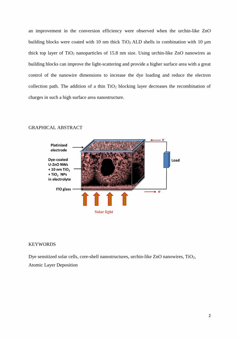
GRAPHICAL ABSTRACT
KEYWORDS
Dye sensitized solar cells, core-shell nanostructures, urchin-like ZnO nanowires, TiO2,
Atomic Layer Deposition
3
INTRODUCTION
The need to find an alternative to oil, and move towards clean and renewable energies,
promotes since the last decades the emergence of new technologies. Among the different
types of renewable energy, photovoltaic energy, based on the direct processing of the sunlight
into electricity, has a significant potential [1]. One of the main objectives in this field of
research is to reduce the processing costs of photovoltaic modules, using widely available and
abundant materials which can be incorporated into a clean manufacturing processes, in order
to create a genuine market competitor to other energy sources (fossil, nuclear, hydro),
considered up to today as less costly. The dye-sensitized solar cell (DSSC) has become a
promising alternative to commercial solar cells due to their low production cost and ease of
fabrication [2-4]. In a DSSC, the photogenerated electrons at the light absorbing dye are
injected to the conduction band of a wide band gap metal oxide nanostructure (i.e. TiO2,
ZnO), to be transported towards the current collector. Subsequently, the dye is regenerated by
the redox couple of the electrolyte (i.e. I/I3-) [5]. Conventional DSSCs consist of a
mesoporous nanocrystalline TiO2 film which possess a large surface area but with numerous
grain boundaries, which ultimately increases the recombination rates of photogenerated
electron-hole pairs and consequently lowers the photovoltaic efficiency [6, 7]. A major
condition for electricity generation with a high photovoltaic efficiency is that the electron-
hole pairs should not recombine (or very rarely). One goal of this study is suppressing the
delicate balance between transport of charges and recombination of electron-hole pairs by
using a specific architecture of semiconductor materials to accelerate electron transport and
minimize recombination of electron-hole pairs by optimizing the nature, structure and
dimensions of the semiconductors.
Alternatively, the use of semiconducting nanowires/nanotubes (e.g., ZnO, TiO2, etc.) as the
nanostructured photoanode offers several advantages such as a high surface area and a direct
4
electron transport owing to the lower amount of grain boundaries that both reduces the
recombination of charges and increases the collection efficiency [8-10]. In addition, the
unique geometry of the nanowires provides an improvement of the optical absorption and
light trapping through a wide range of wavelengths, while reducing optical reflection [11].
Among the n-type semiconductor materials with large band gap, ZnO has been widely
studied due to its non-toxicity and abundance on Earth [12]. For these reasons, ZnO
nanowires are an ideal candidate for a nanostructured photoanode in DSSCs. While the direct
electrical pathways to the electrode provided by the ZnO nanowires ensure the rapid
collection of carriers generated throughout the device, it turns out that the conversion
efficiency is limited by the surface area of the nanowire array [13-15]. These nanostructures
have light harvesting efficiencies below 10 %, which can be improved by increasing the
nanowire surface area with the control of the dimensions of each individual nanowire as
reported in the literature [13, 15]. To tackle this challenge, we previously reported a novel
approach to fabricate well-ordered arrays of hollow urchin-like single-crystal ZnO nanowire
building blocks with controlled nanowire for photovoltaic applications [8, 16]. They were
synthesized by combining the methods of auto-assembly of polystyrene spheres, atomic layer
deposition (ALD), and electrodeposition (ECD) of ZnO nanowires. ALD and ECD are low-
cost and large scalable process for the synthesis of hollow urchin-like ZnO nanowires. [17]
This architecture combined the properties of 1D and 3D materials (higher surface area) and
provided better control of the dimensions of the nanowires. The diameters, density and
morphology of the nanomaterials were adjusted by tuning the growth parameters during the
deposition (ALD and/or ECD), or by modifying the diameter of the PS. The opto-electronic,
structural and morphological properties of these nanostructures impact the photovoltaic
efficiency.
5
In this work, similar Urchin-inspired ZnO nanostructures were prepared and used as building
blocks for the photoanode to fabricate DSSCs. The effect of the growth conditions on the
conversion efficiency of the DSSCs was experimentally evaluated and discussed. Here we
show that the recombination of charges in the urchin-inspired ZnO nanowires dye-sensitized
cells could be decreased and the conversion efficiency enhanced by coating the urchin-like
ZnO nanowire with a conformal TiO2 shell deposited by ALD. ALD is a unique vapor-phase
deposition technique of high quality conformal and homogenous thin films at relatively low
temperatures with a precise thickness control. These properties are ideal for surface and
interface engineering for next generation solar cells [18-21] . Many studies have described the
effects of using insulating or semiconducting thin films of metal oxides as compact and
blocking layers to reduce charge recombination at the different interfaces of the
nanostructured solar cell. These films coating the transparent current collector (i.e. FTO)
and/or the metal oxide nanostructure include Nb2O5, Al2O3, MgO, SrTiO3, SiO2, Y2O3, ZrO2,
SnO2, and TiO2 [22-27]. In general, a layer of oxide semiconductor plays an important role by
passivating the surface defects of the metal oxide nanostructures, as well as adding an energy
barrier that increases the separation between photoinjected electrons and the oxidized redox
species in the electrolyte and consequently reduces recombination of charges [10]. These
barrier recombination layers have to be thin enough to allow efficient photoelectron injection,
and as the thickness decreases, the charge transfer resistance decreases. Therefore, this
highlights the need of ALD to properly control the thickness of such layers. An overview of
such layers deposited using different techniques can be found in reference [28]. A lower rate
of recombination can be translated as a lower dark current (Jdark) and a higher open-circuit
voltage (and fill factor) of a DSSC according to the general expression of the cell open-circuit
voltage (VOC): VOC = nVth ln((JSC/Jdark) + 1), where n is the diode ideality factor and Vth is the
thermal voltage [29]. In addition to reduce the recombination, an energy barrier shell can
6
pointedly increase cell VOC directly if it creates a dipole at the core-shell interface that shifts
the band edge of the core upward in energy [25].
Until now, low conversion efficiencies were obtained when using ZnO nanowires [30], ZnO
nanotubes [31] or ZnO nanoparticles [3, 32] as building blocks for DSSCs. We describe, for
the first time, the ability of a 3D architecture based on urchin-like ZnO nanowires with larger
surface area coated with TiO2 nanostructure to enhance the performance of the DSSCs.
Applying the core-shell concept to an urchin-inspired single crystal ZnO nanowire
photoanode building block as demonstrated in this work provides a means to increase the
electron transport and reduce recombination between nanowire and electrolyte.
MATERIALS AND METHODS
1. Deposition of polystyrene microsphere
A commercially available suspension of polystyrene microsphere (PS) (diameter ~ 5 µm,
4 wt% aqueous dispersion) from Thermo fisher, USA, was used for dip coating transparent
Indium doped tin oxide (ITO) deposited on glass (size 1 x 5 cm2) purchased from Kintec
Company, Hong Kong. Before making the deposition of spheres on the ITO glass, the
substrate was subjected to a specific cleaning technique to remove surface dirt (grease, dust
etc.) collected after manufacturing and during the storage. The cleaning method included,
first, washing the substrates with commercial soap and hot water (~ 90 °C) followed by
rinsing with ultra-purified water. Then the substrates were soaked for 15 minutes in an
ultrasonic bath at 70 °C in three different solvents: trichloroethylene, acetone and isopropanol
and in between rinsed with ultra-pure water heated to 90 °C. The resulting substrates were
dried and stored in plastic boxes to prevent possible contamination prior to deposition. 200 µL
of a carboxylate modified PS microsphere suspension was diluted in 150 µL of ethanol and
7
then dispersed (drop-by-drop using a micro-pipette) onto the surface of deionized water filled
into a Petri dish of 5 cm in diameter to self-assemble for about 12 hours. An ITO substrate
was exposed under a UV lamp for 10 min to promote the adherence of the PS spheres on the
surface of the substrate and then immersed into the suspension. The polystyrene sphere
monolayer was transferred onto the ITO substrate surface by slow removal from the solution
at an angle of 45° [16]. After complete drying of the PS-covered ITO/glass substrate in
furnace at 100 °C for 30 min, the regularly arranged and closely packed spheres were reduced
in diameter using an oxygen plasma treatment by fixing the pressure at 0.7 mbar and the
power supply at 0.2 A. The size of the polystyrene spheres was very accurately controlled by
choosing the appropriate plasma exposure time [6].
2. Synthesis of ZnO Urchins
The ITO covered with PS (ITO/PS) was introduced into a custom made atomic layer
deposition (ALD) reactor for deposition of a ZnO thin film covering homogeneously the
spheres and the ITO substrate surface [9]. The ZnOALD thin films play two important roles: it
is used as a seed layer that controls the growth of the ZnO nanowires, and it renders the
surface electrically active to be used as a conductive electrode for electrodeposition. The
ZnOALD thin films were deposited using diethylzinc (DEZ) and water (H2O). Diethyl Zinc
(DEZ) (Zn(CH2CH3)2, 95% purity, CAS: 557-20-0) was purchased from Sigma Aldrich and
used as zinc source. The ALD was performed by sequential exposures of DEZ and H2O
separated by Argon purge at a flow rate of 100 standard cubic centimeters per minute (sccm).
The regime for the deposition of ZnO consisted of 0.2 s pulses of DEZ, 40 s of exposure to
DEZ, 60 s of Argon purge followed by 2 s pulse of H2O, 40 s exposure to H2O, and a final 60
s Argon purge [16]. This constituted one cycle. ZnO films with 100 ALD cycles were
8
deposited on ITO glass substrates for obtaining 20 nm thick layers of ZnO. The temperature
was fixed at 80°C. The ITO/PS/ZnOALD ensemble was then used as a working electrode for
the electrodeposition of ZnO nanowires by bubbling the oxygen in a three-electrode
electrochemical cell. A platinum wire was used as the counter electrode and an Ag/AgCl
electrode as the reference electrode. The electrolyte was an aqueous solution saturated by
molecular O2 containing zinc chloride as zinc precursor (5.10-4 M) and potassium chloride
(0.1M) as salt. The electrodeposition was performed for a period of 2 to 4 hours by fixing the
potential (-1 V) versus the reference electrode) using an Autolab VERSASTAT3 potentiostat.
The bath temperature was set to 80°C. After electrodeposition, the samples were annealed in
air at 450 °C for 1h to ensure the removal of the PS spheres and the enhancement of the ZnO
nanowires crystallinity. The above process steps defined the hollow urchin-like ZnO
nanowires (U-ZnO NWs) building blocks.
3. Atomic Layer Deposition of TiO2 and Dye-sensitized solar cell Fabrication
The core-shell concept was realized by transferring the urchin-like ZnO nanowires into a
built-in ALD reactor to deposit conformal thin films of TiO2 as recombination barrier layers
with different thicknesses (5, 10, 15, 20, 34 and 42 nm). The deposition of TiO2 was
performed onto the urchin-like ZnO nanowires at a reactor temperature of 60 °C by
alternating the precursors of Titanium Tetra-Isopropoxide (TTIP) heated to 90 °C and H2O
heated to 40 °C. One ALD cycle consisted of a TTIP pulse of 5 s followed by a 10 s exposure,
and 60 s purge, followed by a H2O pulse of 2 s with 10 s exposure and 60 s purge. For some
of the samples, a mesoporous film of TiO2 anatase nanoparticles (P25 Solaronix) was
deposited by doctor blade technique on top of the ZnO/TiO2 core-shell structures.
The samples were then heated to 450 °C in air for 30 min and then immersed in a
solution of 12 mg of Ru dye (N719, Solaronix) diluted in 30 mL of methanol for 12 h. In

9
order to fabricate the cell, the films were rinsed with ethanol, dried, and sandwiched together
to a platinum counter electrode separated by a 60-m-thick hot-melt film (Solaronix). The
internal space of each cell was filled with an iodide electrolyte (AN-50, Solaronix). Cells
were immediately tested under simulated sunlight and illuminated through a black cover with
an aperture of 0.6 cm2.
4. Characterization
The morphology of the samples was observed by scanning electron microscopy (SEM,
Hitachi S-4800). In order to know the elemental composition of samples, energy dispersive X-
ray spectroscopy (EDX) was performed on a JEOL JEM 2200 fs microscope, operated at 200
kV. X-ray diffraction data were obtained on a Bruker D-8 GADDS diffractometer (Co Kα) to
determine the crystalline structures and orientation. Raman spectra were obtained on a Raman
microscope (Nova Spectra, ND-MDT) featuring a laser source with a wavelength of 532 nm
and a 50× objective lens with a numerical aperture of 0.75. Spectra were recorded at a spectral
resolution of 2.7 cm−1 with a laser power below 100 µW so that it does not induce phase
transformation of TiO2; the exposure time was 30 s for all the samples.
The reflectivity of the TiO2-hollow U-ZnO NW building blocks and the absorbance of
TiO2 core-shell U-ZnO NW building blocks were characterized by a spectrophotometer from
Perkin Elmer (Lambda 900). The illumination was carried out from the glass/ ITO side.
Current–voltage (J–V) measurements were made on the DSSCs under half sun illumination
(500 W.m-2). The characteristic parameters of the solar cells, including short-circuit current
density (Jsc), open-circuit voltage (Voc), fill factor (FF) and overall photoconversion efficiency
were extracted from the J–V curves.
RESULTS AND DISCUSSION

10
1. Synthesis and characterization of U-ZnO NWs
Figure 1. SEM images of the U-ZnO NWs: (a) regularly arranged urchin-like ZnO nanowires.
The inset shows a macroscopic view of the deposition. (b) Higher resolution of U-ZnO NWs
after 25 min of PS plasma etching treatment. (c) longitudinal cross sections showing the
growth of ZnO nanowires on the PS and in the gap between them. (d) views of individual U-
ZnO NWs grown on the 20 nm thick ALD ZnO coated PS spheres after plasma etching
treatment of 25 min.
To obtain the unique architecture of U-ZnO NWs, several steps were used, such as: (i)
deposition of an ordered monolayer of PS spheres by dip coating onto an indium doped tin
oxide (ITO) glass substrate, (ii) reduction of the size of the spheres by plasma etching
treatment, (iii) deposition of a uniform conformal thin layer of ZnO (~ 20 nm) by atomic layer
deposition (100 cycles) which renders the surface covered by PS spheres electrically active
for subsequent electrodeposition. In addition, this thin ALD ZnO seed layer serves as a
compact recombination barrier layer to prevent backflow of electrons and avoid short-circuits
between the ITO glass electrode and the electrolyte [33], (iv) electrodeposition of the ZnO
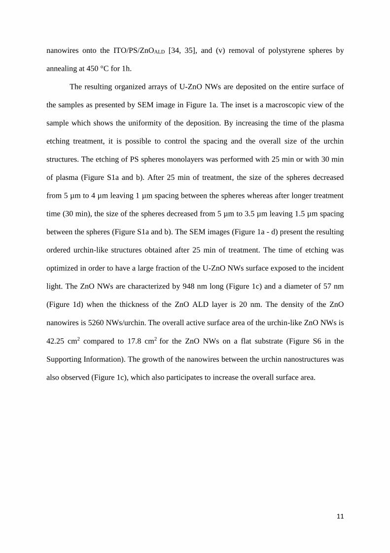
11
nanowires onto the ITO/PS/ZnOALD [34, 35], and (v) removal of polystyrene spheres by
annealing at 450 °C for 1h.
The resulting organized arrays of U-ZnO NWs are deposited on the entire surface of
the samples as presented by SEM image in Figure 1a. The inset is a macroscopic view of the
sample which shows the uniformity of the deposition. By increasing the time of the plasma
etching treatment, it is possible to control the spacing and the overall size of the urchin
structures. The etching of PS spheres monolayers was performed with 25 min or with 30 min
of plasma (Figure S1a and b). After 25 min of treatment, the size of the spheres decreased
from 5 µm to 4 µm leaving 1 µm spacing between the spheres whereas after longer treatment
time (30 min), the size of the spheres decreased from 5 µm to 3.5 µm leaving 1.5 µm spacing
between the spheres (Figure S1a and b). The SEM images (Figure 1a - d) present the resulting
ordered urchin-like structures obtained after 25 min of treatment. The time of etching was
optimized in order to have a large fraction of the U-ZnO NWs surface exposed to the incident
light. The ZnO NWs are characterized by 948 nm long (Figure 1c) and a diameter of 57 nm
(Figure 1d) when the thickness of the ZnO ALD layer is 20 nm. The density of the ZnO
nanowires is 5260 NWs/urchin. The overall active surface area of the urchin-like ZnO NWs is
42.25 cm2 compared to 17.8 cm2 for the ZnO NWs on a flat substrate (Figure S6 in the
Supporting Information). The growth of the nanowires between the urchin nanostructures was
also observed (Figure 1c), which also participates to increase the overall surface area.

12
Figure 2. a) X-ray diffractograms and b) Absorption spectra of ZnO 20 nm ALD layer on a
flat ITO glass substrate and U-ZnO NWs.
EDX analysis confirmed the presence of ZnO as indicated in Table S1. The X-ray
diffraction spectrum of the U-ZnO NWs presented in Figure 2a shows the characteristic peaks
of the ZnO wurtzite structure. The main orientations of the ZnO NWs are (100) at 34.4°,
(002) at 35.2°, and (101) at 36.3° (Figure 2a).
In order to study the influence of U-ZnO NWs on the light scattering, the spectral
dependence of the absorption of the samples was measured (Figure 2b). For all analyzed
samples based on ZnO, the spectra show UV absorbance edge close to 375 nm (3.3 eV),
which corresponds to the band gap energy of ZnO. No absorbance was shown for bare ITO
glass sample. The presence of higher absorbance values is due to the presence of higher
quantity of ZnO. Especially, the formation of urchins increases significantly the absorption by
30% at 372 nm which supports the stronger advantage of using the high surface area U-ZnO
NWs to enhance the light scattering.
2. U-ZnO-TiO2 core-shell nanostructures
2. 1. Synthesis of U-ZnO-TiO2
13
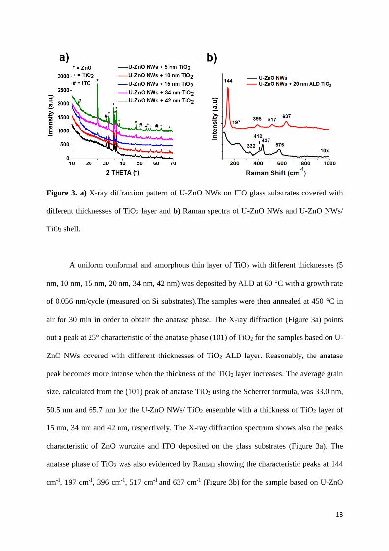
Figure 3. a) X-ray diffraction pattern of U-ZnO NWs on ITO glass substrates covered with
different thicknesses of TiO2 layer and b) Raman spectra of U-ZnO NWs and U-ZnO NWs/
TiO2 shell.
A uniform conformal and amorphous thin layer of TiO2 with different thicknesses (5
nm, 10 nm, 15 nm, 20 nm, 34 nm, 42 nm) was deposited by ALD at 60 °C with a growth rate
of 0.056 nm/cycle (measured on Si substrates).The samples were then annealed at 450 °C in
air for 30 min in order to obtain the anatase phase. The X-ray diffraction (Figure 3a) points
out a peak at 25° characteristic of the anatase phase (101) of TiO2 for the samples based on U-
ZnO NWs covered with different thicknesses of TiO2 ALD layer. Reasonably, the anatase
peak becomes more intense when the thickness of the TiO2 layer increases. The average grain
size, calculated from the (101) peak of anatase TiO2 using the Scherrer formula, was 33.0 nm,
50.5 nm and 65.7 nm for the U-ZnO NWs/ TiO2 ensemble with a thickness of TiO2 layer of
15 nm, 34 nm and 42 nm, respectively. The X-ray diffraction spectrum shows also the peaks
characteristic of ZnO wurtzite and ITO deposited on the glass substrates (Figure 3a). The
anatase phase of TiO2 was also evidenced by Raman showing the characteristic peaks at 144
cm-1, 197 cm-1, 396 cm-1, 517 cm-1 and 637 cm-1 (Figure 3b) for the sample based on U-ZnO
14
NWs / TiO2 20 nm layer ensemble. In the case of the reference sample based on U-ZnO NWs
without TiO2, only peaks of ZnO were observed.
2. 2. Characterization of U-ZnO-TiO2
The spectral dependence of the transmittance of the samples was studied before (Fig.
S3a in the Supporting Information) and after dye loading and subsequent illumination (Fig.
S3b), in order to determine the effect of the thickness of the TiO2 shell on light scattering and
dye loading. A small decrease of the transmittance from 70% to 55% was observed for the
sample U-ZnO NWs/ TiO2 layer when increasing the thickness of the TiO2 layer (Figure S3a).
The reference sample based on U-ZnO NWs without TiO2 has the highest transmittance. The
decrease of the transmittance can be explained by the fact that the thick layer of TiO2 (from
20 nm to 42 nm) absorbs photons and reduces light scattering to the ZnO. This hypothesis
will be analyzed later with the study of the J-V curves of the samples.
The spectral dependence of the transmittance of the samples was also measured after
dye loading and illumination, as shown in Figure S3b. An increase of absorption in the
wavelength range of the excitation of the TiO2 is noticed when increasing the thickness of
TiO2 layer (34 nm and 42 nm) as a consequence of the higher amount of dye loading (Figure
S3b) [36].
The spectral dependence of the optical reflectance of the samples based on U-ZnO
NWs with various thickness of TiO2 shell was also studied (Figure S4 in the Supporting
Information). By increasing the thickness of the TiO2 layer deposited on the U-ZnO NWs, the
maximum of the total reflectance (at λ= 430 nm) increases from 20% to 35% for 5 to 20 nm
TiO2 thickness, respectively, along with a decrease of the reflectance over the whole
wavelength range (Figure S4).
15
2. 3. Solar cell performance of core-shell U-ZnO-TiO2
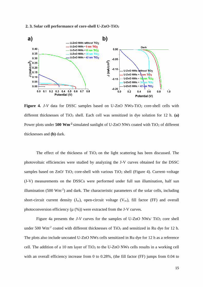
Figure 4. J-V data for DSSC samples based on U-ZnO NWs-TiO2 core-shell cells with
different thicknesses of TiO2 shell. Each cell was sensitized in dye solution for 12 h. (a)
Power plots under 500 Wm-2 simulated sunlight of U-ZnO NWs coated with TiO2 of different
thicknesses and (b) dark.
The effect of the thickness of TiO2 on the light scattering has been discussed. The
photovoltaic efficiencies were studied by analyzing the J-V curves obtained for the DSSC
samples based on ZnO/ TiO2 core-shell with various TiO2 shell (Figure 4). Current–voltage
(J-V) measurements on the DSSCs were performed under full sun illumination, half sun
illumination (500 Wm-2) and dark. The characteristic parameters of the solar cells, including
short-circuit current density (Jsc), open-circuit voltage (Voc), fill factor (FF) and overall
photoconversion efficiency (µ (%)) were extracted from the J-V curves.
Figure 4a presents the J-V curves for the samples of U-ZnO NWs/ TiO2 core shell
under 500 Wm-2 coated with different thicknesses of TiO2 and sensitized in Ru dye for 12 h.
The plots also include uncoated U-ZnO NWs cells sensitized in Ru dye for 12 h as a reference
cell. The addition of a 10 nm layer of TiO2 to the U-ZnO NWs cells results in a working cell
with an overall efficiency increase from 0 to 0.28%, (the fill factor (FF) jumps from 0.04 to
16
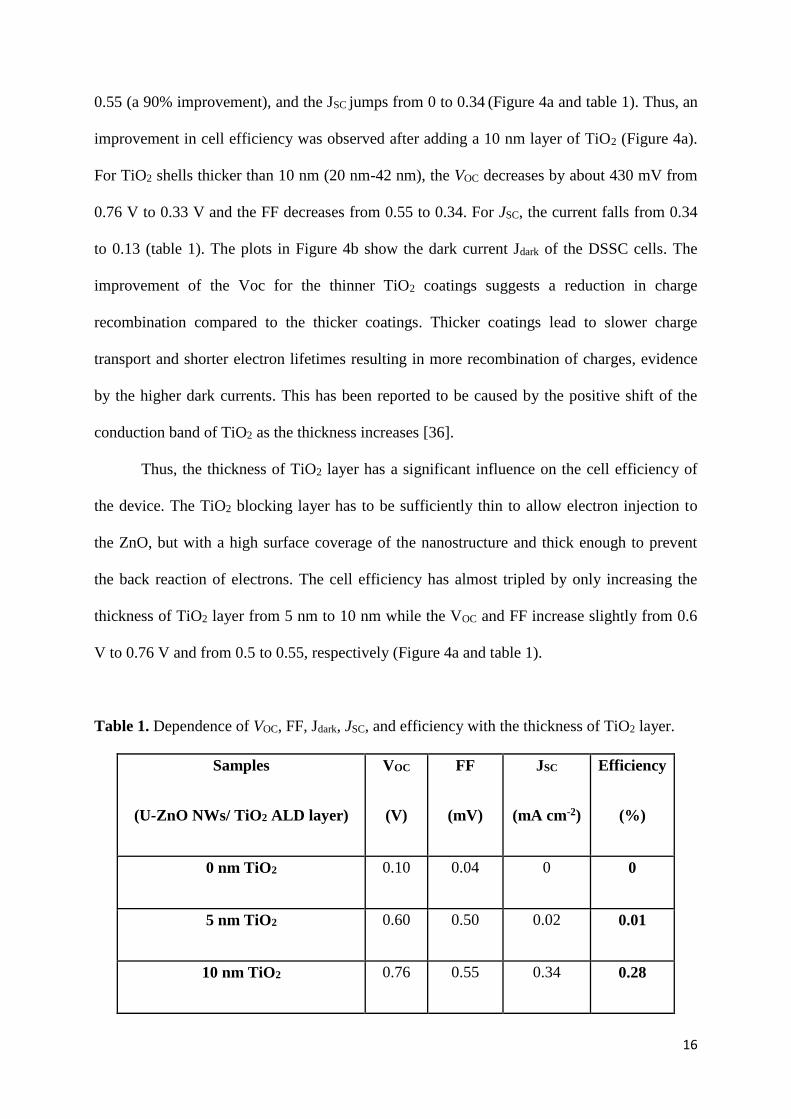
0.55 (a 90% improvement), and the JSC jumps from 0 to 0.34 (Figure 4a and table 1). Thus, an
improvement in cell efficiency was observed after adding a 10 nm layer of TiO2 (Figure 4a).
For TiO2 shells thicker than 10 nm (20 nm-42 nm), the VOC decreases by about 430 mV from
0.76 V to 0.33 V and the FF decreases from 0.55 to 0.34. For JSC, the current falls from 0.34
to 0.13 (table 1). The plots in Figure 4b show the dark current Jdark of the DSSC cells. The
improvement of the Voc for the thinner TiO2 coatings suggests a reduction in charge
recombination compared to the thicker coatings. Thicker coatings lead to slower charge
transport and shorter electron lifetimes resulting in more recombination of charges, evidence
by the higher dark currents. This has been reported to be caused by the positive shift of the
conduction band of TiO2 as the thickness increases [36].
Thus, the thickness of TiO2 layer has a significant influence on the cell efficiency of
the device. The TiO2 blocking layer has to be sufficiently thin to allow electron injection to
the ZnO, but with a high surface coverage of the nanostructure and thick enough to prevent
the back reaction of electrons. The cell efficiency has almost tripled by only increasing the
thickness of TiO2 layer from 5 nm to 10 nm while the VOC and FF increase slightly from 0.6
V to 0.76 V and from 0.5 to 0.55, respectively (Figure 4a and table 1).
Table 1. Dependence of VOC, FF, Jdark, JSC, and efficiency with the thickness of TiO2 layer.
Samples
(U-ZnO NWs/ TiO2 ALD layer)
VOC
(V)
FF
(mV)
JSC
(mA cm-2)
Efficiency
(%)
0 nm TiO2 0.10 0.04 0 0
5 nm TiO2 0.60 0.50 0.02 0.01
10 nm TiO2 0.76 0.55 0.34 0.28

17
20 nm TiO2 0.55 0.47 0.04 0.02
42 nm TiO2 0.33 0.34 0.13 0.03
3. Hybrid structure of nanoparticles and urchins
3.1. Synthesis and characterization of TiO2 nanoparticle on core-shell U-ZnO-TiO2
Figure 5. SEM images of urchin-inspired ZnO-TiO2 core-shell and TiO2 nanoparticle cells.
(a) growth of U-ZnO NWs on 20 nm of ZnOALD seed layer deposited on PS spheres treated
with 25 min of PE treatment; The urchins based ZnO NWs were covered with 10 nm TiO2
anatase (b) U-ZnO NWs / TiO2 10 nm layer / TiO2 NPs ensemble; and (c) inset shows the presence of
TiO2 NPs on the ZnO NWs.
A mesoporous film (10 µm) of anatase TiO2 nanoparticles (TiO2 NPs) was deposited on
the ZnO / TiO2 10 nm layer ensemble in order to further increase the surface area (Fig. 5b and c).
The commercial TiO2 nanoparticles provide a surface area of ~ 100 m2/g (after firing) and a
pore size of 15-20 nm. The overall surface area obtained for the urchins-based ZnO NWs
coated with TiO2 NPs is ~ 113.76 m2/g. Figure 5a presents the urchins based ZnO NWs
18
covered with 10 nm TiO2 anatase without the presence of TiO2 NPs. Figure 5c shows that the
mesoporous TiO2 film does not infiltrate in between the urchins but rather is supported by
them.
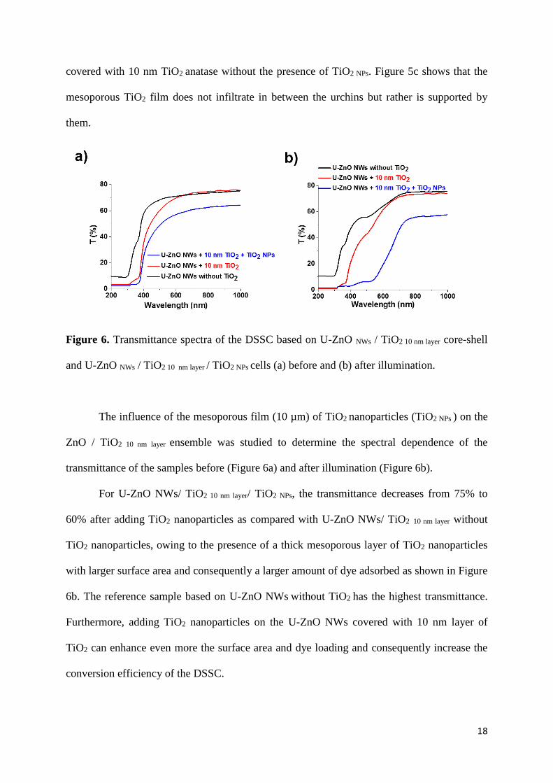
Figure 6. Transmittance spectra of the DSSC based on U-ZnO NWs / TiO2 10 nm layer core-shell
and U-ZnO NWs / TiO2 10 nm layer / TiO2 NPs cells (a) before and (b) after illumination.
The influence of the mesoporous film (10 µm) of TiO2 nanoparticles (TiO2 NPs ) on the
ZnO / TiO2 10 nm layer ensemble was studied to determine the spectral dependence of the
transmittance of the samples before (Figure 6a) and after illumination (Figure 6b).
For U-ZnO NWs/ TiO2 10 nm layer/ TiO2 NPs, the transmittance decreases from 75% to
60% after adding TiO2 nanoparticles as compared with U-ZnO NWs/ TiO2 10 nm layer without
TiO2 nanoparticles, owing to the presence of a thick mesoporous layer of TiO2 nanoparticles
with larger surface area and consequently a larger amount of dye adsorbed as shown in Figure
6b. The reference sample based on U-ZnO NWs without TiO2 has the highest transmittance.
Furthermore, adding TiO2 nanoparticles on the U-ZnO NWs covered with 10 nm layer of
TiO2 can enhance even more the surface area and dye loading and consequently increase the
conversion efficiency of the DSSC.

19
Figure 7. Reflectance spectra of the DSSC based on U-ZnO NWs/ TiO2 10 nm layer core-shell
after illumination as a function of the addition of TiO2 NPs.
The spectral dependence of the optical reflectance of the U-ZnO NWs / TiO2 10 nm layer
core-shell and U-ZnO NWs / TiO2 10 nm layer / TiO2 NPs cells was also studied (Figure 7). In our
three-dimensional architecture based on U-ZnO NWs, the increase of the reflectivity covers a
large wavelength range (400-800 nm). This can be explained due to the fact that nanowires
from ZnO urchins are exposed to the incident light from all angles thanks to the 3D-
architecture. As shown and explained in the transmittance spectra of the DSSC based on ZnO/
TiO2 core-shell after illumination, a broadening in the wavelength range of the reflectance
was noticed after adding TiO2 nanoparticles to the DSSC based on U-ZnO NWs/ TiO2 layer
due to the thick layer of TiO2 nanoparticles (10 µm). The total reflectance (at λ= 600 nm)
increased from 16% to 28% for 10 µm thickness of TiO2 nanoparticles.
3.2. Solar cell performance of hybrid nanoparticle core shell structure

20
Figure 8. J-V data for DSSC samples based on U-ZnO NWs/ TiO2 (10 nm layer) core-shell
cells with and without the addition of TiO2 nanoparticles. Each cell was sensitized in dye
solution for 12 h. Power plots (a) under 500 Wm-2 simulated sunlight and (b) dark. The short-
circuit current density (Jsc), the open-circuit voltage (Voc), the fill factor (FF) and the overall
photoconversion efficiency (µ (%)) are specified for each device.
A considerable improvement of the characteristic parameters of the solar cell based on
U-ZnO NWs/ TiO2 (10 nm layer) was observed after adding TiO2 nanoparticles (U-ZnO NWs/
TiO2 (10 nm layer)/ TiO2 NPs): the cell efficiency improved from 0.28% to 1.8% and the JSC
increased from 0.34% to 2.64%. The VOC decreases slightly from 0.76 V to 0.68 V, while the
FF remains almost the same value (0.5) (Figure 8a and table 2). The improvement in cell
efficiency using the U-ZnO NWs/ TiO2 (10 nm layer) in combination with the TiO2
nanoparticles is mainly due to the increase in surface area and thus the dye loading. However,
low electron transport and recombination mechanisms due to the grain boundaries and surface
defects are still present in the mesoporous TiO2 NP film, as observed from the high dark
currents (Figure 8b). This effect can be further improved by depositing a thin blocking layer
onto the NPs, as reported elsewhere[37]. It has to be noted that the photogenerated electrons
from the adsorbed dye at the mesoporous TiO2 layer are transported through the TiO2 coated
21
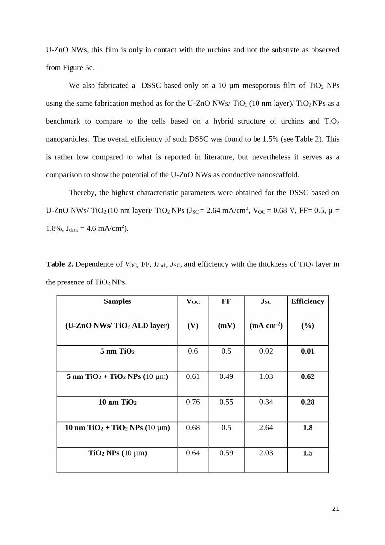
U-ZnO NWs, this film is only in contact with the urchins and not the substrate as observed
from Figure 5c.
We also fabricated a DSSC based only on a 10 µm mesoporous film of TiO2 NPs
using the same fabrication method as for the U-ZnO NWs/ TiO2 (10 nm layer)/ TiO2 NPs as a
benchmark to compare to the cells based on a hybrid structure of urchins and TiO2
nanoparticles. The overall efficiency of such DSSC was found to be 1.5% (see Table 2). This
is rather low compared to what is reported in literature, but nevertheless it serves as a
comparison to show the potential of the U-ZnO NWs as conductive nanoscaffold.
Thereby, the highest characteristic parameters were obtained for the DSSC based on
U-ZnO NWs/ TiO2 (10 nm layer)/ TiO2 NPs (JSC = 2.64 mA/cm2, VOC = 0.68 V, FF= 0.5, µ =
1.8%, Jdark = 4.6 mA/cm2).
Table 2. Dependence of VOC, FF, Jdark, JSC, and efficiency with the thickness of TiO2 layer in
the presence of TiO2 NPs.
Samples
(U-ZnO NWs/ TiO2 ALD layer)
VOC
(V)
FF
(mV)
JSC
(mA cm-2)
Efficiency
(%)
5 nm TiO2 0.6 0.5 0.02 0.01
5 nm TiO2 + TiO2 NPs (10 µm) 0.61 0.49 1.03 0.62
10 nm TiO2 0.76 0.55 0.34 0.28
10 nm TiO2 + TiO2 NPs (10 µm) 0.68 0.5 2.64 1.8
TiO2 NPs (10 µm) 0.64 0.59 2.03 1.5

22
4. Discussion
Table 1 summarizes the VOC, FF, JSC, and efficiency as a function of the thickness of the
TiO2 layer. The VOC and FF increase to 0.76 V and 0.55, respectively, after the deposition of
a 10 nm layer of TiO2, which then gradually decrease by increasing the thickness of the TiO2
layer (20 nm and 42 nm). Increasing the thickness of the TiO2 layer reduces the light
scattering to the ZnO and decreases the electron injection to the ZnO, whereas the thin TiO2
coatings reduce the recombination of charges at the interface while still allowing electron
injection to the ZnO, as observed from the low dark currents.
After adding TiO2 nanoparticles to the U-ZnO NWs – 10 nm TiO2 layer ensemble, the
surface area increases and consequently the dye loading, therefore the overall efficiency
increases up to 1.8 %, regardless of the slight decrease in the VOC (from 0.76 to 0.68 V)
(Table 2). The TiO2 nanoparticles are still subjected to recombination mechanisms and thus
the significant reduction of the Voc onset from dark measurements (Figure 8b). These data
clearly show that thin TiO2 shells enhance VOC and fill factor by reducing the recombination
of electron hole pairs at the oxide-electrolyte interface, which strongly depend on the
thickness of this TiO2 layer (Table 1), highlighting once more the need of ALD to precisely
control the thickness of the film.
Hence, these results show an improvement of the conversion efficiency to 1.8%
compared to 0.8% and 0.7% for ZnO nanowires [14, 30, 38], 0.6% for ZnO nanoparticles [3,
32] and even lower efficiency (0.29%) [31] for ZnO nanotubes through the specific geometry
of ZnO urchins nanowire arrays, and 1.3% for urchins inspired ZnO nanowires [8] by
including a TiO2 recombination barrier layer. The ALD TiO2 layer reduces the recombination
rate of photo injected electrons in the U-ZnO structure that otherwise would have recombined
with either a surface defect or the electrolyte in contact with the U-ZnO structure. The
23
combination of the coated U-ZnO with a mesoporous film of TiO2 nanoparticles increased the
amount of adsorbed dye, increasing the photocurrent and therefore improved the characteristic
parameters of the solar cell. Although, our actual cell efficiencies are still lower than standard
nanoparticle-based solar cells, we demonstrated the use of U-ZnO coated with ALD TiO2 as a
conductive scaffold, as the majority of the current was transported through the urchins. We
believe that there is a possibility to further improve the conversion efficiency by further
optimization of the total surface area of the U-ZnO NWs in addition to the mesoporous TiO2
film or by using a film of perovskite absorber as the light-harvesting active layer [39, 40].
CONCLUSION
Core-shell DSSC cells were fabricated and characterized. The unique 3D architecture of
urchin-like ZnO nanowire arrays have increased the absorbed amount of light due to its larger
surface area compared to ZnO nanowires. The urchin-like ZnO nanowires were prepared by a
low cost technique electrodeposition of ZnO nanowires on polystyrene spheres coated with 20
nm of ZnO by ALD. The resulting U-ZnO nanostructures were coated with conformal and
amorphous TiO2 shells by ALD which were annealed at 450 °C in order to obtain the anatase
phase. These nanostructures were then sensitized with a solution of Ru dye (N719). Coating
the U-ZnO NWs with 5-10 nm of anatase TiO2 has reduced the recombination of charges,
improved the JSC, VOC, FF and consequently the overall conversion efficiency. For TiO2 shells
thicker than 10 nm (20 nm - 42 nm), the transmittance decreases due to a larger absorption of
photons from TiO2, reducing light scattering to the ZnO. Even though thicker TiO2 layers can
adsorb more dye, they lead to lower charge transport resulting in more recombination of
charges, as observed from the higher dark currents. A considerable improvement of the
characteristic parameters of the solar cell was observed after adding a mesoporous film of
TiO2 nanoparticles. Adding TiO2 nanoparticles on the TiO2 coated U-ZnO NWs can increase
24
further the surface area and consequently increase the conversion efficiency of the DSSC,
most likely due to the larger dye loading. Nevertheless, the large surface area of the
nanoparticles, grain boundaries and surface defects still lead to recombination of charges,
which limits the full potential of the cell, which can be improved by depositing another thin
blocking layer to the NPs. Ultimately, it is worth mentioning that the photogenerated current
was transported in its majority through the U-ZnO, which evidences the high conductivity of
such nanostructures, and further optimization may improve the overall conversion efficiency.
ACKNOWLEDGMENTS
This work was financially supported by the joint funding program from the Lebanese
National Council for Scientific Research CNRS-L and the University of Montpellier UM. Dr.
N. Abboud, would like to thank the National Council for Scientific Research in Lebanon for
the support in funding this work. This work was partially supported by CNRS project (PICS
2015-2017 number 233977 NANOALD).
AUTHORS’ CONTRIBUTION
Chantal Karam, Ziad Herro, Nadine Abboud, Sophie Tingry did the electrodeposition and
characterizations of Urchin-Inspired ZnO Nanowires; Mikhael Bechelany and Philippe Miele
did experiments on Atomic layer deposition of ZnO and analyzed the results; Chantal Karam,
Carlos Guerra-Nuñez, Roland Habchi, Antonio Khoury, did the physico-chemical
characterization of the obtained materials and analyzed the obtained results; Chantal Karam,
Ivo Utke and Carlos Guerra-Nuñez did experiments on Atomic layer deposition of TiO2 and
Dye Sensitized Solar Cells; Ivo Utke and Mikhael Bechelany designed the works and write
the manuscript.
25
REFERENCES
1. Makrides, G.Z., Bastian Norton, Matthew Georghiou, George E. Schubert, Markus Werner, Jürgen H., Potential of photovoltaic systems in countries with high solar irradiation. Renewable and Sustainable Energy Reviews, 2010. 14(2): p. 754-762.
2. Gong, J., J. Liang, and K. Sumathy, Review on dye-sensitized solar cells (DSSCs): Fundamental concepts and novel materials. Renewable and Sustainable Energy Reviews, 2012. 16(8): p. 5848-5860.
3. Choudhury, M.S.H., N. Kishi, and T. Soga, Compression of ZnO nanoparticle films at elevated temperature for flexible dye-sensitized solar cells. Journal of Alloys and Compounds, 2016. 656: p. 476-480.
4. Saurdi, I., Shafura, AK, Azhar, NEA, Ishak, A, Malek, MF, Alrokayan, AH Salman, Khan, Haseeb A, Mamat, MH, Rusop, M, Mahmood, Mohamad Rusop. Effect of TiO2 thickness on nanocomposited aligned ZnO nanorod/TiO2 for dye-sensitized solar cells. in AIP Conference Proceedings. 2016. AIP Publishing.
5. Kang Xiaohui, J.C., Wan Zhongquan, Zhuang Jia, Feng, Juan, A novel tri-layered photoanode of hierarchical ZnO microspheres on 1D ZnO nanowire arrays for dye-sensitized solar cells. RSC Advances, 2015. 5(22): p. 16678-16683.
6. Benkstein K. D., K.N., van de Lagemaat J., Frank A. J., Influence of the Percolation Network Geometry on Electron Transport in Dye-Sensitized Titanium Dioxide Solar Cells. The Journal of Physical Chemistry B, 2003. 107(31): p. 7759-7767.
7. Suriati Suhaimi, M.M.S., Z.A. Alahmed, J. Chyský ,A. H. Reshak Materials for Enhanced Dye-sensitized Solar Cell Performance: Electrochemical Application. Int. J. Electrochem. Sci., 2015. 10: p. 2859 - 2871.
8. J. Elias, M.B., I. Utke, R. Erni, D. Hosseini, J. Michler, L. Philippe, Urchin-inspired zinc oxide as building blocks for nanostructured solar cells. Nano Energy, 2012. 1: p. 696–705.
9. Jamil Elias, C.L.v.-C.m., Mikhael Bechelany, Johann Michler, Guillaume-Yangshu Wang, Zhao Wang, and Laetitia Philippe, Hollow Urchin-like ZnO thin Films by Electrochemical Deposition. Adv. Mater., 2010. 22: p. 1607–1612.
10. Matt Law, L.E.G., Aleksandra Radenovic,Tevye Kuykendall, Jan Liphardt, and Peidong Yang*, ZnO-Al2O3 and ZnO-TiO2 Core-Shell Nanowire Dye-Sensitized Solar Cells. J. Phys. Chem. B, 2006. 110: p. 22652-22663.
11. Hiralal Pritesh, C.C., Lal Niraj N, Abeygunasekara Waranatha, Kumar Abhishek, Butt Haider, Zhou Hang, Unalan Husnu Emrah, Baumberg Jeremy J, Amaratunga, Gehan AJ, Nanowire-based multifunctional antireflection coatings for solar cells. Nanoscale, 2014. 6(23): p. 14555-14562.
12. Zaier A., O.E.a.F., Lakfif F., Kabir A., Boudjadar S., Aida M. S., Effects of the substrate temperature and solution molarity on the structural opto-electric properties of ZnO thin films deposited by spray pyrolysis. Materials Science in Semiconductor Processing, 2009. 12(6): p. 207-211.
13. Baxter, J.B. and E.S. Aydil, Nanowire-based dye-sensitized solar cells. Applied Physics Letters, 2005. 86(5): p. 053114.
14. Guillen Elena, A.E., Peter Laurence M., Zukal Arnost, Tena-Zaera Ramon, Anta Juan A., ZnO solar cells with an indoline sensitizer: a comparison between nanoparticulate films and electrodeposited nanowire arrays. Energy & Environmental Science, 2011. 4(9): p. 3400-3407.
15. M. Law, L.E.G., J. C. Johnson, R. Saykally, and P. Yang, Nanowire dye-sensitized solar cells. Nature Materials, 2005. 4(6): p. 455–459.
16. Elias J., U.I., Yoon S., Bechelany M., Weidenkaff A., Michler J., Philippe L., Electrochemical growth of ZnO nanowires on atomic layer deposition coated polystyrene sphere templates. Electrochimica Acta, 2013. 110: p. 387-392.
26
17. Thomas, M.A.C., Jingbiao, Electrodeposition of ZnO nanostructures: growth, doping, and physical properties. Handbook of Nanoelectrochemistry: Electrochemical Synthesis Methods, Properties, and Characterization Techniques, 2016: p. 647-679.
18. Zhang, Y., Guerra-Nunez Carlos, Utke Ivo, Michler Johann, Rossell Marta D, Erni Rolf, Understanding and Controlling Nucleation and Growth of TiO2 Deposited on Multiwalled Carbon Nanotubes by Atomic Layer Deposition. The Journal of Physical Chemistry C, 2015. 119(6): p. 3379-3387.
19. Guerra-Nuñez Carlos, Z.Y., Li Meng, Chawla Vipin, Erni Rolf, Michler Johann, Park Hyung Gyu, Utke Ivo, Morphology and crystallinity control of ultrathin TiO 2 layers deposited on carbon nanotubes by temperature-step atomic layer deposition. Nanoscale, 2015. 7(24): p. 10622-10633.
20. J. A. van Delft, D.G.-A., W. M. M. Kessels, Atomic layer deposition for photovoltaics: applications and prospects for solar cell manufacturing. Semiconductor Science and Technology, 2012. 27(7): p. 074002.
21. Marichy Catherine, B.M., Pinna Nicola, Atomic Layer Deposition of Nanostructured Materials for Energy and Environmental Applications. Advanced Materials, 2012. 24(8): p. 1017-1032.
22. Bandaranayake, K.M.P.S., M. K. I.; Weligamuwa, P. M. G. M. P.; Tennakone, K., Coord. Chem. ReV., 2004. 248: p. 1277.
23. Kirthi Tennakone, J.B., Priyangi Konara Mudiyanselage, Bandaranayake, Gamaralalage Rajanya Asoka, Kumara, Akinori, Konno, Enhanced Efficiency of a Dye-Sensitized Solar Cell Made from MgO-Coated Nanocrystalline SnO 2. Japanese Journal of Applied Physics, 2001. 40(7B): p. L732.
24. Palomares Emilio, C.J.N., Haque, Saif A., Lutz Thierry, Durrant James R., Control of Charge Recombination Dynamics in Dye Sensitized Solar Cells by the Use of Conformally Deposited Metal Oxide Blocking Layers. Journal of the American Chemical Society, 2003. 125(2): p. 475-482.
25. Yishay Diamant, S.C., S.G. Chen, Ophira Melamed, Arie Zaban, Core–shell nanoporous electrode for dye sensitized solar cells: the effect of shell characteristics on the electronic properties of the electrode. Coordination Chemistry Reviews, 2004. 248: p. 1271–1276.
26. Yishay Diamant, S.G.C., Ophira Melamed, and Arie Zaban*, Core-Shell Nanoporous Electrode for Dye Sensitized Solar Cells: the Effect of the SrTiO3 Shell on the Electronic Properties of the TiO2 Core. J. Phys. Chem. B, 2003. 107: p. 1977-1981.
27. Zaban A., C.S.G., Chappel S., Gregg B. A., Bilayer nanoporous electrodes for dye sensitized solar cells. Chemical Communications, 2000(22): p. 2231-2232.
28. Saxena, V. and D.K. Aswal, Surface modifications of photoanodes in dye sensitized solar cells: enhanced light harvesting and reduced recombination. Semiconductor Science and Technology, 2015. 30(6): p. 064005.
29. Greene, L.E., Next-generation photovoltaics using solution-grown zinc oxide nanowire arrays. 2007: ProQuest.
30. Marimuthu T., A.N., Thangamuthu R., Mummoorthi M., Ravi G., Synthesis of ZnO nanowire arrays on ZnOTiO2 mixed oxide seed layer for dye sensitized solar cell applications. Journal of Alloys and Compounds, 2016. 677: p. 211-218.
31. Rahman M. Y. A., R.L., Umar A. A., Salleh M. M., Effect of boric acid composition on the properties of ZnO thin film nanotubes and the performance of dye-sensitized solar cell (DSSC). Journal of Alloys and Compounds, 2015. 648: p. 86-91.
32. Sobuś Jan, B.G., Karolczak Jerzy, Idígoras Jesús, Anta Juan A., Ziółek Marcin, Comparison of TiO2 and ZnO Solar Cells Sensitized with an Indoline Dye: Time-Resolved Laser Spectroscopy Studies of Partial Charge Separation Processes. Langmuir, 2014. 30(9): p. 2505-2512.
33. Elias, J., R. Tena-Zaera, and C. Lévy-Clément, Electrodeposition of ZnO nanowires with controlled dimensions for photovoltaic applications: Role of buffer layer. Thin Solid Films, 2007. <HT>515</HT>(24): p. 8553-8557.
27
34. Peulon, S. and D. Lincot, Cathodic electrodeposition from aqueous solution of dense or open-structured zinc oxide films. Advanced Materials, 1996. 8(2): p. 166-170.
35. R.Tena-Zaera, J.E., G.Wang, C.Levy-Clement, Journal of Physical Chemistry C 2007. 111: p. 16706.
36. Li Luping, X.C., Zhao Yang, Chen Shikai, Ziegler Kirk J, Improving performance via blocking layers in dye-sensitized solar cells based on nanowire photoanodes. ACS applied materials & interfaces, 2015. 7(23): p. 12824-12831.
37. Chandiran, A.K., et al., Sub-nanometer conformal TiO(2) blocking layer for high efficiency solid-state perovskite absorber solar cells. Advanced Materials, 2014. 26(25): p. 4309-12.
38. Qi Junjie, L.W., Biswas Chandan Zhang, Guangjie, Sun Lifang, Wang Zengze, Hu Xiaofeng, Zhang Yue, Enhanced power conversion efficiency of CdS quantum dot sensitized solar cells with ZnO nanowire arrays as the photoanodes. Optics Communications, 2015. 349: p. 198-202.
39. Ball, J.M., Lee, Michael M., Hey, Andrew, Snaith, Henry J., Low-temperature processed meso-superstructured to thin-film perovskite solar cells. Energy & Environmental Science, 2013. 6(6): p. 1739-1743.
40. Liu, M., M.B. Johnston, and H.J. Snaith, Efficient planar heterojunction perovskite solar cells by vapour deposition. Nature, 2013. 501(7467): p. 395-398.