Vertical single-crystal ZnO nanowires grown on ZnO:Ga/glass templates
6
IEEE TRANSACTIONS ON NANOTECHNOLOGY, VOL. 4, NO. 6, NOVEMBER 2005 649 Vertical Single-Crystal ZnO Nanowires Grown on ZnO : Ga/Glass Templates Cheng-Liang Hsu, Shoou-Jinn Chang, Hui-Chuan Hung, Yan-Ru Lin, Chorng-Jye Huang, Yung-Kuan Tseng, and I.-Cherng Chen Abstract—Vertical single-crystal ZnO nanowires with uni- form diameter and uniform length were selectively grown on ZnO : Ga/glass templates at 600 C by a self-catalyzed vapor–liquid–solid process without any metal catalyst. It was found that the ZnO nanowires are grown preferred oriented in the direction with a small X-ray diffraction full-width half-maximum. Photoluminescence, field-emission scanning electron microscopy, and high-resolution transmission electron microscopy measurements also confirmed good crystal quality of our ZnO nanowires. Field emitters using these ZnO nanowires were also fabricated. It was found that threshold field of the fabricated field emitters was 14 V/ m. With an applied electric field of 24 V/ m, it was found that the emission current density was around 0.1 mA/cm Index Terms—Field emission, field-emission scanning elec- tron microscopy (FESEM), glass, high-resolution transmis- sion electron microscopy (HRTEM), photoluminescence (PL), vapor–liquid–solid (VLS) process, X-ray diffraction (XRD), ZnO nanowires. I. INTRODUCTION O NE-DIMENSIONAL (1-D) semiconductor nanowires and nanorods have attracted great attention in recent years due to their potential applications in both nanoscale electronic and opto-electronic devices. Although many studies have been performed on Si and III–V nanowire systems, [1]–[4], only a few reports on 1-D oxide systems can be found in the literature. These 1-D oxide systems include SnO , [5] SiO , [6] GeO , [7] ZnO, [8], [9] indium tin oxide (ITO), [10] and Al O [11]. Among them, ZnO is an n-type semiconductor with a large exciton binding energy of 60 meV and a wide bandgap energy of 3.37 eV at room temperature. ZnO emits short-wavelength light, conducts transparently, and is piezoelectric. Previously, Huang et al. [12] reported the successful gas phase synthesis of ZnO nanowires on patterned Au catalyst by vapor–liquid–solid (VLS) reaction at high temperatures (i.e., 900 C–925 C). Manuscript received October 12, 2004; revised February 16, 2005. C.-L. Hsu is with the Department of Electrical Engineering and the Depart- ment of Electronic Engineering, Ming Chi University of Technology, Taishan, Taipei, Taiwan, R.O.C. S.-J. Chang and H.-C. Hung are with the Institute of Microelectronics and the Department of Electrical Engineering, National Cheng Kung University, Tainan, Taiwan, R.O.C. Y.-R. Lin, C.-J. Huang, and I-C. Chen are with the Materials Research Lab- oratories, Industrial Technology Research Institute, Hsinchu, Taiwan, R.O.C. (e-mail: [email protected]). Y.-K. Tseng is with the Department and Graduate School of Cultural Heritage Conservation, National Yunlin University of Science and Technology, Yunlin, Taiwan, R.O.C. Digital Object Identifier 10.1109/TNANO.2005.851394 Geng et al. [13] modified this VLS technology and successfully grew ZnO nanowires on an Si substrate. On the other hand, glass substrates are transparent and low cost. Large area glass substrates are also commercially avail- able. Thus, glass is an ideal substrate material for large-size opto-electronic devices. If we can grow ZnO nanowires directly on glass substrates, we should be able to realize various novel opto-electronic devices such as ZnO-based light emitters, photodetectors, and field-emission displays (FEDs). However, it is difficult to grow ZnO nanowires on glass substrates by the high-temperature VLS method since glass substrates are amor- phous and weak at high temperatures. Very recently, Tseng et al. [14] developed a low-temperature VLS process and demon- strated the selective area growth of ZnO nanowires at 550 C. They also reported the growth of vertical single-crystal ZnO nanowires on ZnO : Ga/Si N /SiO /Si templates [15]. In this study, we report the low-temperature growth of ZnO nanowires on ZnO : Ga/glass templates at 600 C by a self-catalyzed VLS process without any metal catalyst. The physical, optical, and field-emission properties of the deposited ZnO nanowires will also be discussed. II. SAMPLE AND EXPERIMENTAL DETAILS Our synthesis was performed by vapor phase transport depo- sition. Zinc vapor source is Zn metal powder with the purity of 99.9% purchased from Strem Chemicals. Prior to the deposition of ZnO nanowires, we first deposited a 50-nm-thick Ga-doped ZnO film directly on glass substrates by RF sputtering. From X-ray diffraction (XRD) measurements, it was found that the sputtered ZnO : Ga film was preferred oriented at the di- rection. Four-point resistivity measurement shows that the sheet resistance of the ZnO : Ga film is around 200 /sq. Standard photolithography and wet etching were then performed to de- fine the stripe patterns with a stripe width of 10 m on the templates. The spacing between the stripes was also 10 m. During wet etching, the template was dipped in HCl(2%) for 3 min to remove the exposed regions of the ZnO : Ga layer. We then placed the patterned ZnO : Ga/glass template together with zinc vapor source on an alumina boat, and inserted them into a quartz tube of furnace. Constant streams of argon (i.e., 54.4 sccm) and oxygen (i.e., 0.8 sccm) gases were then intro- duced into the furnace. It should be noted that we carefully controlled the positions of the patterned ZnO : Ga/glass tem- plate, zinc vapor source and alumina boat so that they were lo- cated at the same horizontal level and were heated at the same temperature. The distance between the zinc vapor source and ZnO : Ga/glass template was also maintained at 20 mm with the 1536-125X/$20.00 © 2005 IEEE Authorized licensed use limited to: National Cheng Kung University. Downloaded on December 24, 2008 at 03:35 from IEEE Xplore. Restrictions apply.
Transcript of Vertical single-crystal ZnO nanowires grown on ZnO:Ga/glass templates
IEEE TRANSACTIONS ON NANOTECHNOLOGY, VOL. 4, NO. 6, NOVEMBER 2005 649
Vertical Single-Crystal ZnO NanowiresGrown on ZnO : Ga/Glass Templates
Cheng-Liang Hsu, Shoou-Jinn Chang, Hui-Chuan Hung, Yan-Ru Lin, Chorng-Jye Huang, Yung-Kuan Tseng,and I.-Cherng Chen
Abstract—Vertical single-crystal ZnO nanowires with uni-form diameter and uniform length were selectively grownon ZnO : Ga/glass templates at 600 C by a self-catalyzedvapor–liquid–solid process without any metal catalyst. It wasfound that the ZnO nanowires are grown preferred oriented inthe (002) direction with a small X-ray diffraction full-widthhalf-maximum. Photoluminescence, field-emission scanningelectron microscopy, and high-resolution transmission electronmicroscopy measurements also confirmed good crystal quality ofour ZnO nanowires. Field emitters using these ZnO nanowireswere also fabricated. It was found that threshold field of thefabricated field emitters was 14 V/ m. With an applied electricfield of 24 V/ m, it was found that the emission current densitywas around 0.1 mA/cm2
Index Terms—Field emission, field-emission scanning elec-tron microscopy (FESEM), glass, high-resolution transmis-sion electron microscopy (HRTEM), photoluminescence (PL),vapor–liquid–solid (VLS) process, X-ray diffraction (XRD), ZnOnanowires.
I. INTRODUCTION
ONE-DIMENSIONAL (1-D) semiconductor nanowiresand nanorods have attracted great attention in recent years
due to their potential applications in both nanoscale electronicand opto-electronic devices. Although many studies have beenperformed on Si and III–V nanowire systems, [1]–[4], only afew reports on 1-D oxide systems can be found in the literature.These 1-D oxide systems include SnO , [5] SiO , [6] GeO ,[7] ZnO, [8], [9] indium tin oxide (ITO), [10] and Al O [11].Among them, ZnO is an n-type semiconductor with a largeexciton binding energy of 60 meV and a wide bandgap energyof 3.37 eV at room temperature. ZnO emits short-wavelengthlight, conducts transparently, and is piezoelectric. Previously,Huang et al. [12] reported the successful gas phase synthesis ofZnO nanowires on patterned Au catalyst by vapor–liquid–solid(VLS) reaction at high temperatures (i.e., 900 C–925 C).
Manuscript received October 12, 2004; revised February 16, 2005.C.-L. Hsu is with the Department of Electrical Engineering and the Depart-
ment of Electronic Engineering, Ming Chi University of Technology, Taishan,Taipei, Taiwan, R.O.C.
S.-J. Chang and H.-C. Hung are with the Institute of Microelectronics and theDepartment of Electrical Engineering, National Cheng Kung University, Tainan,Taiwan, R.O.C.
Y.-R. Lin, C.-J. Huang, and I-C. Chen are with the Materials Research Lab-oratories, Industrial Technology Research Institute, Hsinchu, Taiwan, R.O.C.(e-mail: [email protected]).
Y.-K. Tseng is with the Department and Graduate School of Cultural HeritageConservation, National Yunlin University of Science and Technology, Yunlin,Taiwan, R.O.C.
Digital Object Identifier 10.1109/TNANO.2005.851394
Geng et al. [13] modified this VLS technology and successfullygrew ZnO nanowires on an Si substrate.
On the other hand, glass substrates are transparent and lowcost. Large area glass substrates are also commercially avail-able. Thus, glass is an ideal substrate material for large-sizeopto-electronic devices. If we can grow ZnO nanowires directlyon glass substrates, we should be able to realize various novelopto-electronic devices such as ZnO-based light emitters,photodetectors, and field-emission displays (FEDs). However,it is difficult to grow ZnO nanowires on glass substrates by thehigh-temperature VLS method since glass substrates are amor-phous and weak at high temperatures. Very recently, Tseng etal. [14] developed a low-temperature VLS process and demon-strated the selective area growth of ZnO nanowires at 550 C.They also reported the growth of vertical single-crystal ZnOnanowires on ZnO : Ga/Si N /SiO /Si templates [15]. In thisstudy, we report the low-temperature growth of ZnO nanowireson ZnO : Ga/glass templates at 600 C by a self-catalyzed VLSprocess without any metal catalyst. The physical, optical, andfield-emission properties of the deposited ZnO nanowires willalso be discussed.
II. SAMPLE AND EXPERIMENTAL DETAILS
Our synthesis was performed by vapor phase transport depo-sition. Zinc vapor source is Zn metal powder with the purity of99.9% purchased from Strem Chemicals. Prior to the depositionof ZnO nanowires, we first deposited a 50-nm-thick Ga-dopedZnO film directly on glass substrates by RF sputtering. FromX-ray diffraction (XRD) measurements, it was found that thesputtered ZnO : Ga film was preferred oriented at the di-rection. Four-point resistivity measurement shows that the sheetresistance of the ZnO : Ga film is around 200 /sq. Standardphotolithography and wet etching were then performed to de-fine the stripe patterns with a stripe width of 10 m on thetemplates. The spacing between the stripes was also 10 m.During wet etching, the template was dipped in HCl(2%) for3 min to remove the exposed regions of the ZnO : Ga layer.We then placed the patterned ZnO : Ga/glass template togetherwith zinc vapor source on an alumina boat, and inserted theminto a quartz tube of furnace. Constant streams of argon (i.e.,54.4 sccm) and oxygen (i.e., 0.8 sccm) gases were then intro-duced into the furnace. It should be noted that we carefullycontrolled the positions of the patterned ZnO : Ga/glass tem-plate, zinc vapor source and alumina boat so that they were lo-cated at the same horizontal level and were heated at the sametemperature. The distance between the zinc vapor source andZnO : Ga/glass template was also maintained at 20 mm with the
1536-125X/$20.00 © 2005 IEEE
Authorized licensed use limited to: National Cheng Kung University. Downloaded on December 24, 2008 at 03:35 from IEEE Xplore. Restrictions apply.
650 IEEE TRANSACTIONS ON NANOTECHNOLOGY, VOL. 4, NO. 6, NOVEMBER 2005
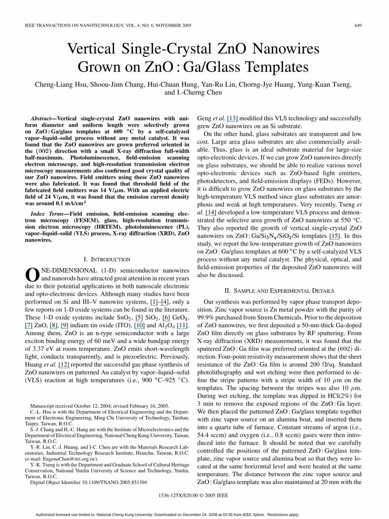
Fig. 1 (a)–(c) FE-SEM image shows the ZnO nanowires were selectivelygrown on ZnO : Ga/glass templates.
zinc vapor source placed at the upstream side. A mechanicalpump was then used to evacuate the system and a programmabletemperature controller was used to preciously control the fur-nace temperature with an accuracy of 1 C. During the growthof ZnO nanowires, the pressure inside the quartz tube, growthtemperature and growth time were kept at 10 torr, 600 C, and20 min, respectively.
A Philips PW3710 X-ray diffractometer and a JEOLJEM-2100F transmission electron microscopy (TEM), operatedat 200 kV, were then used to characterize the crystallographicand structural properties of the as-grown ZnO nanowires. Sur-face morphologies of the samples and size distribution of thenanowires were characterized by a LEO 1530 field-emissionscanning electron microscope (FESEM), operated at 5 keV.Photoluminescence (PL) properties of these as-grown ZnOnanowires were also characterized by a Jobin Yvon-Spexfluorolog-3 spectrophotometer. During PL measurements, anXe lamp emitting at 254 nm was used as the excitation source.Room-temperature field-emission properties of these ZnOnanowires were also investigated in a vacuum chamber with apressure of 5–9 10 torr. During field-emission measure-ments, a tungsten probe with a diameter of 1.8 mm was used asthe anode, while the interelectrode distance between anodeand ZnO nanowires was preciously controlled at 15 m. AKeithley 237 high-voltage source was then used to provide thesweeping electric field and to monitor the emission current.
III. RESULTS AND DISCUSSION
Fig. 1(a)–(c) shows FESEM images of the as-grown sampleviewed with a 25 title angle. It can be clearly seen that high-density vertical ZnO nanowires with uniform diameter and uni-form length were selectively grown on ZnO : Ga/glass templatesat 600 C. It should be noted that ZnO nanowires can onlybe grown on the sputtered ZnO : Ga layer. In other words, nonanowires could be grown directly on the glass substrate wherethe sputtered ZnO : Ga layer was etched. It should also be notedthat we clearly observed the boundary of these ZnO nanowireswhile no disordered ZnO nanowires were found. Fig. 2 showsa cross-sectional FESEM image of the ZnO nanowires grown
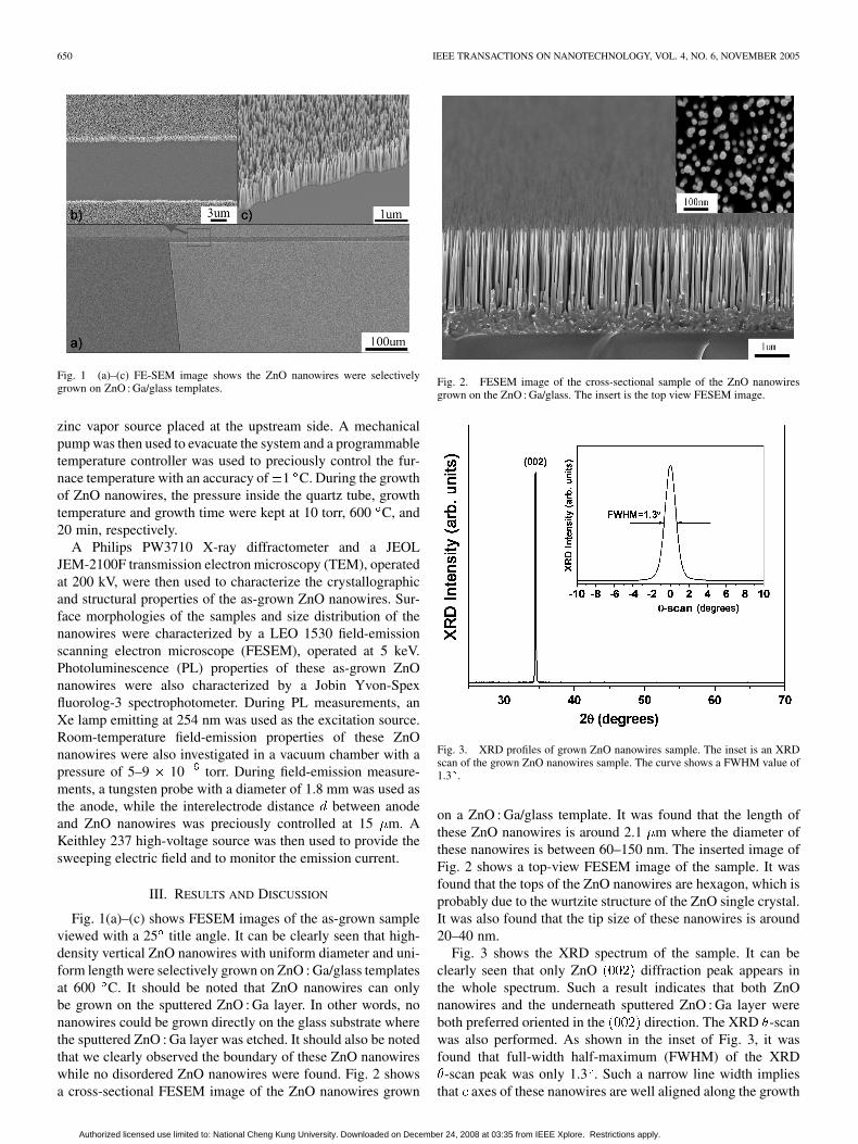
Fig. 2. FESEM image of the cross-sectional sample of the ZnO nanowiresgrown on the ZnO : Ga/glass. The insert is the top view FESEM image.
Fig. 3. XRD profiles of grown ZnO nanowires sample. The inset is an XRDscan of the grown ZnO nanowires sample. The curve shows a FWHM value of1.3 .
on a ZnO : Ga/glass template. It was found that the length ofthese ZnO nanowires is around 2.1 m where the diameter ofthese nanowires is between 60–150 nm. The inserted image ofFig. 2 shows a top-view FESEM image of the sample. It wasfound that the tops of the ZnO nanowires are hexagon, which isprobably due to the wurtzite structure of the ZnO single crystal.It was also found that the tip size of these nanowires is around20–40 nm.
Fig. 3 shows the XRD spectrum of the sample. It can beclearly seen that only ZnO diffraction peak appears inthe whole spectrum. Such a result indicates that both ZnOnanowires and the underneath sputtered ZnO : Ga layer wereboth preferred oriented in the direction. The XRD -scanwas also performed. As shown in the inset of Fig. 3, it wasfound that full-width half-maximum (FWHM) of the XRD
-scan peak was only 1.3 . Such a narrow line width impliesthat axes of these nanowires are well aligned along the growth
Authorized licensed use limited to: National Cheng Kung University. Downloaded on December 24, 2008 at 03:35 from IEEE Xplore. Restrictions apply.
HSU et al.: VERTICAL SINGLE-CRYSTAL ZnO NANOWIRES GROWN ON ZnO : Ga/GLASS TEMPLATES 651
Fig. 4. TEM image of the cross-sectional sample of the ZnO nanowires grownon the ZnO : Ga/glass.
Fig. 5. (a) High-resolution TEM image of an individual ZnO nanowireshowing its [001] growth direction. The inset shows the correspondingselected-area electron diffraction pattern from the nanowires.
direction, which also agrees with the hexagon tips observed inthe inserted images of Fig. 2. Fig. 4 shows the cross-sectionalhigh-resolution transmission electron microscopy (HRTEM)image of the ZnO nanowires. The brightness contrast observedin this image could be attributed to the diffraction patternsoriginated from various crystal-graphic planes. We thus believethat the sputtered ZnO layer should has a grainy and columnarstructure, while the ZnO nanowires were grown along thecolumnar grains of the sputtered ZnO layer.
Fig. 5(a) shows a selected area electron diffraction (SAED)image of the sample. Such a diffraction pattern also indicatesthat our ZnO nanowires are single crystal with a wurtzite na-ture. Fig. 5(b) and (c) shows HRTEM images taken from thetip portion and sidewall portion of the ZnO nanowires, respec-tively. It can be clearly seen that the ZnO crystal lattices are welloriented with no observable defects in both regions. Such a re-sult indicates our ZnO nanowires are structurally uniform anddefect free. The 0.52-nm lattice spacing observed from thesetwo figures is equivalent two ZnO crystal planes. Fig. 6shows an energy-dispersive X-ray (EDX) spectrum of our ZnOnanowires. It was found that our nanowires contain 53% zinc
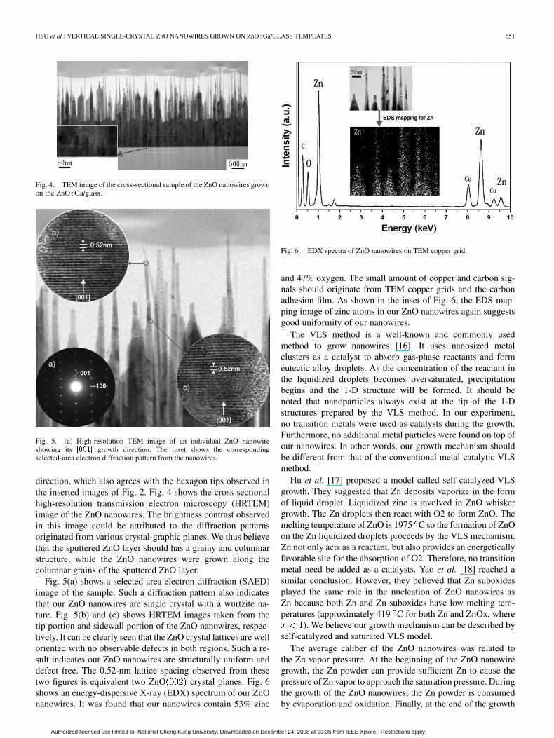
Fig. 6. EDX spectra of ZnO nanowires on TEM copper grid.
and 47% oxygen. The small amount of copper and carbon sig-nals should originate from TEM copper grids and the carbonadhesion film. As shown in the inset of Fig. 6, the EDS map-ping image of zinc atoms in our ZnO nanowires again suggestsgood uniformity of our nanowires.
The VLS method is a well-known and commonly usedmethod to grow nanowires [16]. It uses nanosized metalclusters as a catalyst to absorb gas-phase reactants and formeutectic alloy droplets. As the concentration of the reactant inthe liquidized droplets becomes oversaturated, precipitationbegins and the 1-D structure will be formed. It should benoted that nanoparticles always exist at the tip of the 1-Dstructures prepared by the VLS method. In our experiment,no transition metals were used as catalysts during the growth.Furthermore, no additional metal particles were found on top ofour nanowires. In other words, our growth mechanism shouldbe different from that of the conventional metal-catalytic VLSmethod.
Hu et al. [17] proposed a model called self-catalyzed VLSgrowth. They suggested that Zn deposits vaporize in the formof liquid droplet. Liquidized zinc is involved in ZnO whiskergrowth. The Zn droplets then react with O2 to form ZnO. Themelting temperature of ZnO is 1975 C so the formation of ZnOon the Zn liquidized droplets proceeds by the VLS mechanism.Zn not only acts as a reactant, but also provides an energeticallyfavorable site for the absorption of O2. Therefore, no transitionmetal need be added as a catalysts. Yao et al. [18] reached asimilar conclusion. However, they believed that Zn suboxidesplayed the same role in the nucleation of ZnO nanowires asZn because both Zn and Zn suboxides have low melting tem-peratures (approximately 419 C for both Zn and ZnOx, where
). We believe our growth mechanism can be described byself-catalyzed and saturated VLS model.
The average caliber of the ZnO nanowires was related tothe Zn vapor pressure. At the beginning of the ZnO nanowiregrowth, the Zn powder can provide sufficient Zn to cause thepressure of Zn vapor to approach the saturation pressure. Duringthe growth of the ZnO nanowires, the Zn powder is consumedby evaporation and oxidation. Finally, at the end of the growth
Authorized licensed use limited to: National Cheng Kung University. Downloaded on December 24, 2008 at 03:35 from IEEE Xplore. Restrictions apply.

652 IEEE TRANSACTIONS ON NANOTECHNOLOGY, VOL. 4, NO. 6, NOVEMBER 2005
Fig. 7. PL emission spectra excited at � = 254 nm show a strong emissionat approximately 376 nm. The insertion image is the PL spectra from 30 to 300K.
process, the source could not easily supply Zn vapor and the tipsof the nanowires became sharp.
Fig. 7 shows a room-temperature PL spectrum of the ZnOnanowires. It can be clearly seen that the PL spectrum exhibitsa strong peak located at approximately 376 nm and a long tailin the long wavelength region. The strong PL peak can be at-tributed to the recombination of free excitons through an ex-citon–exciton collision process [19]. Deep level emissions (i.e.,green–yellow bands) are also observed as the long tail shown inFig. 7. It has been suggested that deep level emissions are re-lated to the singly ionized oxygen vacancy in ZnO [20]. Previ-ously, it has been shown that defect related emissions are orig-inated from radiative transitions between oxygen vacancy re-lated shallow donors [21]. Since the acceptor level (i.e., Zn va-cancy) and the donor level are located at 2.5 and 0.05–0.19 eVbelow the conduction band edge, respectively, the strong exci-tonic emission and the very weak deep level emission again indi-cate high optical quality of our ZnO nanowires. To further inves-tigate the origins of the tentatively assigned excitonic emissionpeaks, we performed PL measurements at low temperatures, asshown in the inset of Fig. 7. From these temperature-dependentPL spectra, it was found that PL intensity of the peak locatedat 370 nm (i.e., excitonic peak) increased with increasing tem-perature from 30 to 300 K due to the thermally induced disso-ciation of electron–hole pairs. Previously, Park et al. [22] ob-served four peaks from their low-temperature PL spectra. How-ever, only one PL peak was observed from our ZnO nanowires.This again suggests a high quality of our nanowires.
Fig. 8 shows field-emission characteristics of our ZnOnanowires grown on a ZnO : Ga/glass template. It was foundthat the threshold voltage of this field emitter was 420 V(i.e., applied electric field V m since interelectrodedistance m). In other words, no field emission oc-curred when the applied voltage was smaller than the 420 V.Above threshold, it was found that the emission currentincreased linearly as the applied electric field was further in-creased. With an applied voltage of 720 V (i.e., applied electricfield V/ m), we achieved an emission current of
Fig. 8. Emission current–voltage characteristics of ZnO nanowires. The insetis FN plots of ln(I=V ) against (1=V ).
0.1 mA/cm . However, the emission current starts to saturatewhen the applied voltage is higher than 720 V. The field-emis-sion characteristics of our ZnO nanowires could be describedby the Fowler–Nordheim (FN) equation
where is the current density (A/m ), is the applied voltage(V), is the field enhancement factor, (AeV/V ), (V/m eV ), and is the work functionof ZnO nanowires (eV), which is around 5.3 eV [23]. To furtherinvestigate the field-emission behavior of our ZnO nanowires,we re-plotted as a function of . As shown inthe FN plot in the inset of Fig. 8, it was found that there ex-hibit two different linear regions within the measured range. Thechange in the slope of the FN plot indicates that the local elec-tric field at the top of these nanowires might not increase linearlywith the applied voltage. From this FN plot, we found that thefield enhancement factor was around 407. These field-emis-sion characteristics resemble those in pertinent literature [15].Collins and Zettl [24] found that space charge sharply reducesthe actual electric field at the emitter when the current densitiesare high. The space charge becomes significant because the localelectric field is no longer proportional to the applied voltage sothe FN linearity criterion does not apply. The saturation of theemitter current due to limited carrier concentration in a non-metallic emitter can enhance this space–charge effect. The com-bination of space–charge buildup and carrier saturation explainsthe sharp breakpoints observed in the field-emission character-istics of semiconductors. Their results further indicated that cur-rent saturation was accompanied by an increase in emission cur-rent fluctuations, but they attributed this to interactions betweenneighboring nanotube tips.
IV. DISCUSSION
In summary, vertical single-crystal ZnO nanowires withuniform diameter and uniform length were selectively grownon ZnO : Ga/glass templates at 600 C by a self-catalyzed
Authorized licensed use limited to: National Cheng Kung University. Downloaded on December 24, 2008 at 03:35 from IEEE Xplore. Restrictions apply.

HSU et al.: VERTICAL SINGLE-CRYSTAL ZnO NANOWIRES GROWN ON ZnO : Ga/GLASS TEMPLATES 653
VLS process without any metal catalyst. It was found thatthe ZnO nanowires are grown preferred oriented in thedirection with a small XRD FWHM. PL, FESEM, and HRTEMmeasurements also confirmed good crystal quality of our ZnOnanowires. Field emitters using these ZnO nanowires were alsofabricated. It was found that the threshold field of the fabricatedfield emitters was 14 V/ m. With an applied electric field of24 V/ m, it was found that the emission current density wasaround 0.1 mA/cm .
REFERENCES
[1] C. C. Chen and C. C. Yeh, “Large-scale catalytic synthesis of crystallinegallium nitride nanowires,” Adv. Mater., vol. 12, pp. 738–741, May 2000.
[2] J. Zhu and S. Fan, “Nanostructure of GaN and SiC nanowires based oncarbon nanotubes,” J. Mater. Res., vol. 14, pp. 1175–1177, Apr. 1999.
[3] X. F. Duan and C. M. Lieber, “General synthesis of compound semicon-ductor nanowires,” Adv. Mater., vol. 12, pp. 298–302, Feb. 2000.
[4] Y. Homma, P. Finnie, T. Ogino, H. Noda, and T. Urisu, “Aligned islandformation using step-band networks on Si(111),” J. Appl. Phys., vol. 83,pp. 3083–3088, Sep. 1999.
[5] Z. R. Dai, Z. W. Pan, and Z. L. Wang, “Novel nanostructures offunctional oxides synthesized by thermal evaporation,” Adv. FunctionalMater., vol. 13, pp. 9–24, Jan. 2003.
[6] Y. Q. Zhu, W. B. Hu, W. K. Hsu, M. Terrones, N. Grobert, J. P. Hare,H. W. Kroto, D. R. M. Walton, and H. Terrones, “Generation of hollowcrystalline tungsten oxide fibers,” Appl. Phys. A, Mater. Sci. Process.,vol. 70, pp. 231–233, Feb. 2000.
[7] Z. G. Bai, D. P. Yu, H. Z. Zhang, Y. Ding, X. Z. Gai, Q. L. Hang, G.C. Xiong, and S. Q. Feng, “Nano-scale GeO wires synthesized byphysical evaporation,” Chem. Phys. Lett., vol. 303, pp. 311–314, Apr.1999.
[8] Z. W. Pan, Z. R. Dai, and Z. L. Wang, “Nanobelts of semiconductingoxides,” Science, vol. 291, pp. 1947–1949, Mar. 2001.
[9] J. J. Wu and S.-C. Liu, “Low-temperature growth of well-aligned ZnOnanorods by chemical vapor deposition,” Adv. Mater., vol. 14, pp.215–218, Jan. 2002.
[10] H. Yumoto, T. Sako, Y. Gotoh, K. Nishiyama, and T. Kaneko, “Growthmechanism of vapor–liquid–solid (VLS) grown indium tin oxide (ITO)whiskers along the substrate,” J. Cryst. Growth, vol. 203, pp. 136–140,May 1999.
[11] V. Valcarcel, A. Souto, and F. Guitian, “Development of single-crystal�–Al O fibers by vapor–liquid–solid deposition (VLS) from alu-minum and powdered silica,” Adv. Mater., vol. 10, pp. 138–140, Jan.1999.
[12] M. H. Huang, Y. Wu, H. Feick, N. Tran, E. Weber, and P. Yang, “Cat-alytic growth of zinc oxide nanowires by vapor transport,” Adv. Mater.,vol. 13, pp. 113–116, Jan. 2001.
[13] C. Geng, Y. Jiang, Y. Yao, X. Meng, J. A. Zapien, C. S. Lee, Y. Lifshitz,and S. T. Lee, “Well-aligned ZnO nanowire arrays fabricated on siliconsubstrates,” Adv. Functional Mater., vol. 14, pp. 589–594, Jun. 2004.
[14] Y. K. Tseng, H. C. Hsu, W. F. Hsieh, K. S. Liu, and I. C. Chen, “Two-stepoxygen injection process for growing ZnO nanorods,” J. Mater. Res., vol.18, pp. 2837–2844, Dec. 2003.
[15] Y. K. Tseng, C. J. Huang, H. M. Cheng, I. N. Lin, K. S. Liu, and I.C. Chen, “Characterization and field-emission properties of needle-likezinc oxide nanowires grown vertically on conductive zinc oxide films,”Adv. Functional Mater., vol. 13, pp. 811–814, Oct. 2003.
[16] P. Yang, “Semiconductor nanowire array,” Proc. SPIE–Int. Soc. Opt.Eng., vol. 4806, pp. 222–224, Jul. 2002.
[17] J. Q. Hu, Q. Li, N. B. Wong, C. S. Lee, and S. T. Lee, “Synthesis ofuniform hexagonal prismatic ZnO Whiskers,” Chem. Mater., vol. 14, pp.1216–1219, Feb. 2002.
[18] B. D. Yao, Y. F. Chan, and N. Wang, “Formation of ZnO nanostructuresby a simple way of thermal evaporation,” Appl. Phys. Lett., vol. 81, pp.757–759, Jul. 2002.
[19] S. C. Lyu, Y. Zhang, H. Ruh, H.-J. Lee, H.-W. Shim, E.-K. Suh, and C. J.Lee, “Low temperature growth and photoluminescence of well-alignedzinc oxide nanowires,” Chem. Phys. Lett., vol. 363, pp. 134–138, Sep.2002.
[20] B. J. Jin, S. H. Bae, S. Y. Lee, and S. Im, “Effects of native defects onoptical and electrical properties of ZnO prepared by pulsed laser depo-sition,” Mater. Sci. Eng. B, vol. 71, pp. 301–305, Feb. 2000.
[21] H.-J. Egelhaaf and D. Oelkrug, “Luminescence and nonradiative deac-tivation of excited states involving oxygen defect centers in polycrys-talline ZnO,” J. Cryst. Growth, vol. 161, pp. 190–194, Apr. 1996.
[22] W. I. Park, Y. H. Jun, S. W. Jung, and G. C. Yi, “Metalorganic vapor-phase epitaxial growth of vertically well-aligned ZnO nanorods,” Appl.Phys. Lett., vol. 80, pp. 4232–4234, Jun. 2002.
[23] T. Minami, T. Miyata, and T. Yamamoto, “Work function of transparentconducting multicomponent oxide thin films prepared by magnetronsputtering,” Surf. Coat. Technol., vol. 108–109, pp. 588–593, Oct. 1998.
[24] P. G. Collins and A. Zettl, “Unique characteristics of cold cathode-carbon-nanotube matrix field emitters,” Phys. Rev. B, Condens. Matter,vol. 55, pp. 9391–9399, Apr. 1997.
Cheng-Liang Hsu was born in Taipei, Taiwan,R.O.C., in 1973. He received the B.S. degree inelectronic engineering from Chung-Yuan ChristianUniversity, Chung-Li, Taiwan, R.O.C., in 1996, theM.S. degree in electronic engineering from the Na-tional Taiwan University of Science and Technology(NTUST), Taipei, Taiwan, R.O.C., in 1998, and iscurrently working toward the Ph.D. degree at theInstitute of Microelectronics, National Cheng-KungUniversity (NCKU), Tainan, Taiwan, R.O.C.
From 2000 to 2003, was an Engineer with theTaiwan Semiconductor Manufacturing Company (TSMC), during which timehe specialized in CMOS low-voltage low-kelvin devices and 0.13-�m copperprocess. His current research interests focus on nanoscale 1-D semiconductors.
Shoou-Jinn Chang was born in Taipei, Taiwan,R.O.C., on January 17, 1961. He received theB.S.E.E. degree from National Cheng Kung Uni-versity (NCKU), Tainan, Taiwan, R.O.C., in 1983,the M.S.E.E. degree from the State University ofNew York, Stony Brook, in 1985, and the Ph.D.degree in electrical engineering from the Universityof California at Los Angeles, in 1989.
From 1989 to 1992, he was a Research Scientistwith National Telephone and Telegraph (NTT) BasicResearch Laboratories, Musashino, Japan. In 1992,
he became an Associate Professor with the Electrical Engineering Department,NCKU, and became a Full Professor in 1998. He also currently serves as theDirector of the Semiconductor Research Center, NCKU. From January 1999to March 1999, he was a Royal Society Visiting Scholar with the Universityof Wales, Swansea, U.K. From July 1999 to February 2000, he was a VisitingScholar with the Research Center for Advanced Science and Technology, Uni-versity of Tokyo, Tokyo, Japan. From August 2001 to September 2001, he wasa Visiting Scholar with the Institute of Microstructural Science, National Re-search Council. From August 2002 to September 2002, he was a Visiting Scholarwith the Institute of Physics, Stuttgart University, Stuttgart, Germany. From July2004 to September 2004, he was a Visiting Scholar with Waseda University. Heis also an Honorary Professor with the Changchun University of Science andTechnology. His current research interests include semiconductor physics andopto-electronic devices.
Hui-Chuan Hung was born in Haohsiung, Taiwan,R.O.C., in 1962. He received the B.S. degree in elec-tronic physic from National Chiao Tung University(NCTU), Hsin-Chu, Taiwan, R.O.C., in 1987, and iscurrently working toward the M.S. degree at the Insti-tute of Microelectronics, National Cheng-Kung Uni-versity (NCKU), Tainan, Taiwan, R.O.C.
From 1989 to 1993, he was an Engineer withthe Electronics Research and Service Organization(ERSO)/Industrial Technology Research InstituteITRI, where he specialized in an 0.8-�m process.
From 1993 to 1998, he was a Section Manager with the United Microelec-tronics Corporation (UMC), where he specialized in failure analysis on an0.8–0.35-�m process. Since 1998, he has been a Manager with the TaiwanSemiconductor Manufacturing Company (TSMC), Taiwan, R.O.C., where hespecialized in failure analysis on a 0.35–0.13-�m low-kelvin copper process.
Authorized licensed use limited to: National Cheng Kung University. Downloaded on December 24, 2008 at 03:35 from IEEE Xplore. Restrictions apply.

654 IEEE TRANSACTIONS ON NANOTECHNOLOGY, VOL. 4, NO. 6, NOVEMBER 2005
Yan-Ru Lin was born in Yunlin, Taiwan, R.O.C.,in 1973. He received the B.S. degree in materialsengineering from Tatung University, Taipei, Taiwan,R.O.C., in 1995, and the Doctorate degree inmaterials science and engineering from NationalTsing-Hua University, Hsinchu, Taiwan, R.O.C., in2003.
His current research interests focus on nanoscale1-D semiconductor and epitaxial growth of III–V andII–VI materials.
Chorng-Jye Huang was born in Tainan, Taiwan,R.O.C., in 1964. He received the B.S. and M.S.degrees in electronic engineering from Chung-YuanChristian University, Chung-Li, Taiwan, R.O.C., in1986 and 1988, respectively, and the Ph.D. degreein electronic engineering from National Chiao TungUniversity, Hsinchu, Taiwan, R.O.C., in 1992.
Since 1992, he has been with the Materials Re-search Laboratories, Industrial Technology and Re-search Institute, Taiwan, R.O.C. His current researchinterests is the development of photovoltaic devices
and nanodevices.
Yung-Kuan Tseng was born in Pingtung, Taiwan,R.O.C., in 1965. He received the B.E. and M.E.degrees in chemistry from National Sun-Yet-SenUniversity, Kaohsiung, Taiwan, R.O.C., in 1989and 1991, respectively, and the Ph.D. degrees inmaterials science and engineering from NationalTsing-Hua University, Hsinchu, Taiwan, R.O.C., in2003.
From 2000 to 2004, he was with the Material Re-search Laboratories, Industrial Technology ResearchInstitute, where he contributed to the development of
the synthesis of nanoscale materials. In 2004, he joined the Department andGraduate School of Cultural Heritage Conservation, National Yunlin Univer-sity of Science and Technology, Yunlin, Taiwan, R.O.C., where he is currentlyan Assistant Professor. His current research interests focus on characterizationof structures and properties of nanoscale materials.
I.-Cherng Chen was born in Hsinchu, Taiwan,R.O.C., in 1961. He received the B.S. degreein chemistry from Tamkang University, Taiwan,R.O.C., in 1985, and the M.S. degrees in nuclearscience on radio chemistry from National Tsing HuaUniversity (NTHU), Hsinchu, Taiwan, R.O.C., in1987, and the Ph.D. degree in applied chemistryfrom National Chiao Tung University (NCTU),Taiwan, R.O.C., in 2001.
In September 1987, he joined the Materials Re-search Laboratories (MRL), Industrial Technology
Research Institute (ITRI), Taiwan, R.O.C., where he has been dedicated to thedevelopment of chemical sensors materials and technology for 13 years. He iscurrently involved with nanoscale 1-D semiconductors and their electrodeviceapplication.
Authorized licensed use limited to: National Cheng Kung University. Downloaded on December 24, 2008 at 03:35 from IEEE Xplore. Restrictions apply.