
Influence of process variables on growth of ZnO nanowires by cathodic electrodeposition on zinc...
7
Influence of process variables on growth of ZnO nanowires by cathodic electrodeposition on zinc substrate Farid Jamali Sheini a, 1 , I.S. Mulla b , Dilip S. Joag c , Mahendra A. More c, ⁎ a Islamic Azad University, Ahwaz Branch, Ahwaz, Iran b Physical and Materials Chemistry Division, National Chemical Laboratory, Pune-411008, India c Center for Advanced Studies in Materials Science and Condensed Matter Physics, Department of Physics, University of Pune, Pune-411007, India abstract article info Article history: Received 16 August 2008 Received in revised form 16 April 2009 Accepted 20 April 2009 Available online 23 April 2009 Keywords: Electrodeposition Zinc oxide Nanowires Annealing Scanning electron microscopy Transmission electron microscopy Photoluminescence Influence of the deposition duration and electrolyte concentration on the structural and morphological features of the ZnO thin films, grown by cathodic electrodeposition on zinc substrate followed by annealing in air at 400 °C, have been investigated. The surface morphology of the as-synthesized films shows two distinct features, presence of ‘2-dimensional nanosheets’ on the area near the electrolyte–air interface and ‘granular’ nanostructures, below the interface region. However, upon annealing, the formation of ZnO nanowires, possessing length of several microns and diameter less than 20 nm, on the entire substrate is observed. The X-ray and selected area electron diffraction patterns clearly confirm the polycrystalline nature of the ZnO nanowires. © 2009 Elsevier B.V. All rights reserved. 1. Introduction One dimensional nanostructures have attracted a great deal of attention because of their unique electronic, optical, chemical and thermal properties resulting from their low dimensionality. Amongst the various semiconducting nanostructures, Zinc oxide (ZnO) nanos- tructures have been intensively studied due to their potential applications in diversified areas. The potential for technological application of ZnO originates from its unique properties such as wide direct band gap of ~3.37 eV and large excitonic binding energy of 60 meV (at room temperature), high mechanical strength, excellent thermal and chemical stability at harsh operating conditions. In addition to these, low electron affinity and high aspect ratio of the ZnO nanostructures are advantageous from the point of view of their use as cold emitters in field emission based devices [1–3]. Till to day, possibly the largest number of nanostructures have been known for ZnO. Some of these are nanowires, nanocombs, nanobelts, nanonails, nano- flowers, nanotetrapods, nanorings and nanorods [4–7]. Numerous techniques are employed to synthesize the ZnO nanos- tructures which include, thermal evaporation [8–17] pulsed laser deposition [18], chemical vapor deposition [19,20], plasma-assisted molecular beam epitaxy [21], sonochemical method [22] and electro- chemical deposition [23–30]. The cathodic electrodeposition has been recognized as one of the effective methods to prepare nanomaterials as it is a simple, economic, non-vacuum and low temperature method facilitating ease of scaling up to the industrial level. By varying the process parameters such as applied potential difference, concentration and pH of the electrolyte, operating temperature and time of deposition, etc., the growth rate, the film morphology and its thickness can be controlled as per the requirement. Usually, ZnO electrodeposition is based on the reduction of an oxygen precursor including chloride [23–26], nitrate [27], hydrogen peroxide [28] and dissolved O 2 [29]. In most of these studies conducting glass has been used as substrate [23,26–28]. Recently, G. Zou et al. have reported orientation enhancement of polycrystalline ZnO thin films through thermal oxidation of electrochemically deposited Zn thin films on conducting glass substrates [31]. Despite a large body of published work on electrodeposition of nanostructured ZnO thin films, a report on systematic studies exploring the influence of process variables on the structural and morphological properties of the electrodeposited ZnO thin films is lacking. In this paper, we report electrochemical synthesis of ZnO nanostructures on Zn substrate from aqueous electrolytic bath. Influence of the process variables such as deposition time and concentration of the electrolyte on the structural and morphological properties of the ZnO nanostructures has been systematically studied. Upon annealing of the samples in air at 400 °C for 4 h, formation of ZnO nanowires with high number density and high aspect ratio is observed. A possible mechanism describing the evolution of different morphologies and growth of the ZnO nanostructures is discussed. Thin Solid Films 517 (2009) 6605–6611 ⁎ Corresponding author. Tel.: +91 20 25692678; fax: +9120 25691684. E-mail address: [email protected] (M.A. More). 1 Present address: Department of Physics, University of Pune, Pune — 411007, India. 0040-6090/$ – see front matter © 2009 Elsevier B.V. All rights reserved. doi:10.1016/j.tsf.2009.04.046 Contents lists available at ScienceDirect Thin Solid Films journal homepage: www.elsevier.com/locate/tsf
-
Upload
independent -
Category
Documents
-
view
6 -
download
0
Transcript of Influence of process variables on growth of ZnO nanowires by cathodic electrodeposition on zinc...
Thin Solid Films 517 (2009) 6605–6611
Contents lists available at ScienceDirect
Thin Solid Films
j ourna l homepage: www.e lsev ie r.com/ locate / ts f
Influence of process variables on growth of ZnO nanowires by cathodicelectrodeposition on zinc substrate
Farid Jamali Sheini a,1, I.S. Mulla b, Dilip S. Joag c, Mahendra A. More c,⁎a Islamic Azad University, Ahwaz Branch, Ahwaz, Iranb Physical and Materials Chemistry Division, National Chemical Laboratory, Pune-411008, Indiac Center for Advanced Studies in Materials Science and Condensed Matter Physics, Department of Physics, University of Pune, Pune-411007, India
⁎ Corresponding author. Tel.: +91 20 25692678; fax:E-mail address: [email protected] (M.A
1 Present address: Department of Physics, University
0040-6090/$ – see front matter © 2009 Elsevier B.V. Adoi:10.1016/j.tsf.2009.04.046
a b s t r a c t
a r t i c l e i n f oArticle history:Received 16 August 2008Received in revised form 16 April 2009Accepted 20 April 2009Available online 23 April 2009
Keywords:ElectrodepositionZinc oxideNanowiresAnnealingScanning electron microscopyTransmission electron microscopyPhotoluminescence
Influence of the deposition duration and electrolyte concentration on the structural and morphologicalfeatures of the ZnO thin films, grown by cathodic electrodeposition on zinc substrate followed by annealingin air at 400 °C, have been investigated. The surface morphology of the as-synthesized films shows twodistinct features, presence of ‘2-dimensional nanosheets’ on the area near the electrolyte–air interface and‘granular’ nanostructures, below the interface region. However, upon annealing, the formation of ZnOnanowires, possessing length of several microns and diameter less than 20 nm, on the entire substrate isobserved. The X-ray and selected area electron diffraction patterns clearly confirm the polycrystalline natureof the ZnO nanowires.
© 2009 Elsevier B.V. All rights reserved.
1. Introduction
One dimensional nanostructures have attracted a great deal ofattention because of their unique electronic, optical, chemical andthermal properties resulting from their low dimensionality. Amongstthe various semiconducting nanostructures, Zinc oxide (ZnO) nanos-tructures have been intensively studied due to their potentialapplications in diversified areas. The potential for technologicalapplication of ZnO originates from its unique properties such as widedirect band gap of ~3.37 eV and large excitonic binding energy of60 meV (at room temperature), high mechanical strength, excellentthermal and chemical stability at harsh operating conditions. Inaddition to these, low electron affinity and high aspect ratio of the ZnOnanostructures are advantageous from the point of view of their use ascold emitters in field emission based devices [1–3]. Till to day, possiblythe largest number of nanostructures have been known for ZnO. Someof these are nanowires, nanocombs, nanobelts, nanonails, nano-flowers, nanotetrapods, nanorings and nanorods [4–7].
Numerous techniques are employed to synthesize the ZnO nanos-tructures which include, thermal evaporation [8–17] pulsed laserdeposition [18], chemical vapor deposition [19,20], plasma-assistedmolecular beam epitaxy [21], sonochemical method [22] and electro-
+91 20 25691684.. More).of Pune, Pune — 411007, India.
ll rights reserved.
chemical deposition [23–30]. The cathodic electrodeposition has beenrecognized as one of the effective methods to prepare nanomaterials as itis a simple, economic, non-vacuum and low temperature methodfacilitating ease of scaling up to the industrial level. By varying the processparameters such as applied potential difference, concentration and pH ofthe electrolyte, operating temperature and time of deposition, etc., thegrowth rate, the film morphology and its thickness can be controlled asper the requirement. Usually, ZnO electrodeposition is based on thereduction of an oxygen precursor including chloride [23–26], nitrate [27],hydrogen peroxide [28] and dissolved O2 [29]. In most of these studiesconducting glass has been used as substrate [23,26–28]. Recently, G. Zouet al. have reported orientation enhancement of polycrystalline ZnO thinfilms through thermal oxidation of electrochemically deposited Zn thinfilmsonconductingglass substrates [31].Despite a largebodyofpublishedwork on electrodeposition of nanostructured ZnO thin films, a report onsystematic studies exploring the influence of process variables on thestructural and morphological properties of the electrodeposited ZnO thinfilms is lacking. In this paper, we report electrochemical synthesis of ZnOnanostructures on Zn substrate from aqueous electrolytic bath. Influenceof the process variables such as deposition time and concentration of theelectrolyte on the structural and morphological properties of the ZnOnanostructures has been systematically studied. Upon annealing of thesamples in air at 400 °C for 4 h, formation of ZnO nanowires with highnumber density and high aspect ratio is observed. A possible mechanismdescribing the evolution of differentmorphologies and growth of the ZnOnanostructures is discussed.
6606 F. Jamali Sheini et al. / Thin Solid Films 517 (2009) 6605–6611
2. Experimental procedure
The synthesis was carried out in a conventional three electrodeelectrochemical cell in aqueous solution containing a mixture of ZnCl2andH2O2 (analytical grade) as a supportingelectrolyte. Theuse ofH2O2 isconvenient since it is highly soluble in the aqueousmediumanddoes notproduce undesirable by-products upon reduction. All deposition experi-ments were carried out at 82 °C, inwhich a polycrystalline Zn foil (purity~99.99%, Alfa Aesar), platinum sheet and a saturated calomel electrode(SCE, E0=0.244 V) were used as the working, counter and referenceelectrodes, respectively. In order to reveal the influence of the processvariables, depositions were made using electrolytes of different molarconcentrations, 0.002 M (ZnCl2=0.002 M and 0.01 M H2O2), 0.004 M(ZnCl2=0.004 M and 0.02 M H2O2), 0.016 M (ZnCl2=0.016 M and0.04MH2O2) anddeposition intervals of 10, 20, 30 and 40min durations.A computer controlled electrochemical analyzer (Model-1100A Series,CH Instrument, USA) was used to maintain the cathodic polarizationcondition at −1.4 V with respect to the SCE. The electrolyte wasconstantly stirred during the deposition. Prior to each electrodepositionexperiment, the substrate and the platinumelectrodewereultrasonicallycleaned in acetone andmethanol, for 10min in each solvent, respectively.The working electrode (Zn foil), after the fixed deposition time, wasremoved from the electrolyte and dried in air. For each case, the ‘as-synthesized’ thin filmwas annealed in air at ~400 °C for 4 h.
The thin films were characterized by using X-ray diffractometer(XRD, Model-D8, Advance, Bruker AXS), scanning electron microscope(SEM, JEOL, JSM-6360A) and transmission electron microscope (TEM,Technai, TM G2 F30). The elemental composition was obtained usingenergy-dispersive X-ray spectrometer (EDS) attached to the SEM. TheXRD was used in 2θ mode (20°–80°) with operating voltage of ~20 kVand the CuKα (λ: 1.5406 Å) as the radiation source. The SEM imageswere recordedwith an accelerating voltage ~20 kV and filament current~60 µA. The EDS spectrawere obtained fromat least four tofive differentspots (total area ~25µm2) and the collectiondurationwas~80 s, for eachspot. The EDS spectrometerwas calibrated using a standard specimen ofgold. For theTEManalysis specimenswere prepared by scraping the ZnOthin film from the substrates. The scraped material was dispersed andsonicated in acetone. A small quantity of this solutionwas dropped on tothe gold coated copper grid. The TEM images were grabbed at anaccelerating voltage of 300 kV. The optical properties were investigatedfrom thephotoluminescence (PL) spectra recordedat room temperatureusing a Xenon lamp as the source (Photoluminescence Spectrometer,Perkin Elmer-LS-55). The exciting wavelength was ~325 nm.
3. Results and discussion
The cathodic electrodeposition of ZnO from aqueous solution ofzinc salt occurs as per the following reactions [21]:
H2O2 þ 2e−→2OH
− ð1Þ
Zn2þ þ 2OH
−→ZnðOHÞ2 ð2ÞZnðOHÞ2→ZnO þ H2O ð3Þ
In the first step, hydroxide ions are generated at the surface of thecathode (working electrode) by the reduction of an oxygen precursor(Eq. (1)) which reacts chemically with Zn+2 ions in the solution toform Zn(OH)2 at the cathode (Eq. (2)). Subsequently, Zn(OH)2 isspontaneously dehydrated into ZnO particles on the working elec-trode (Eq. (3)).
In order to study the influence of deposition time and concentra-tion of the electrolyte, initially the deposition time was optimized and
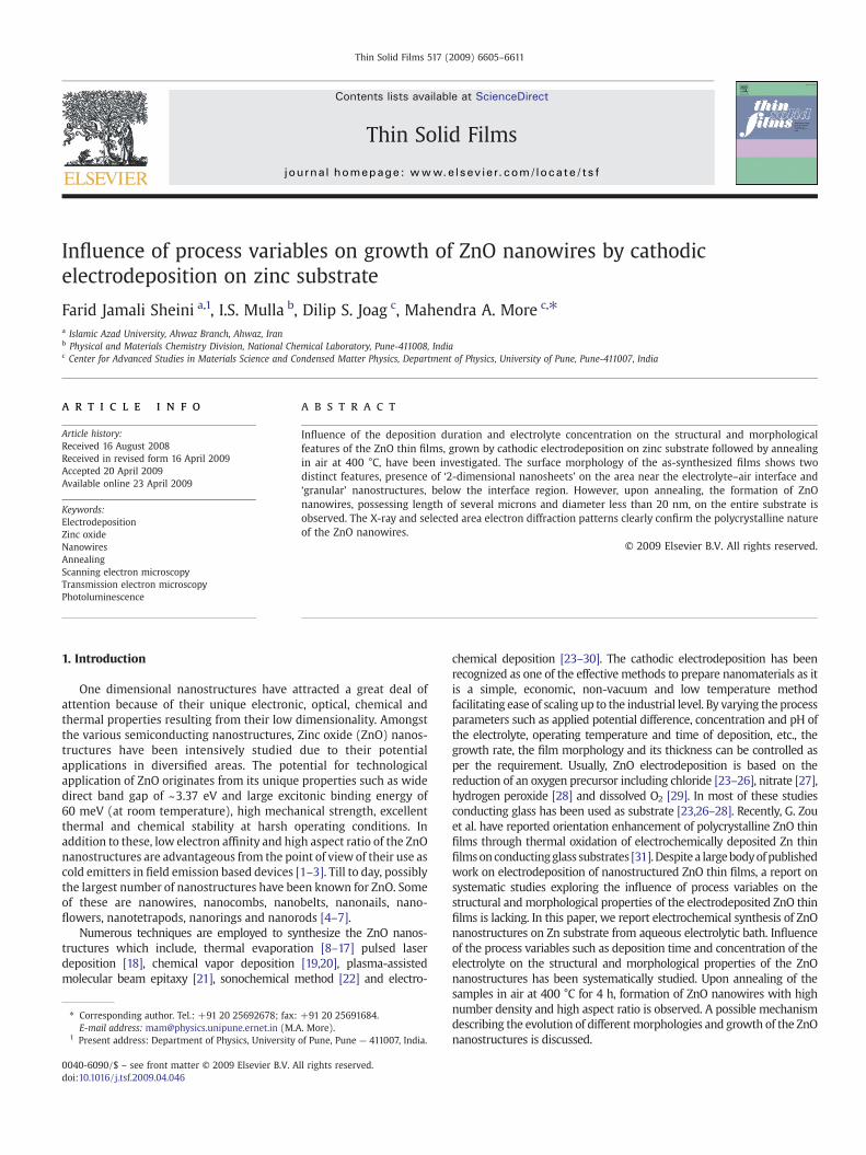
Fig. 1. SEM images of the as-synthesized ZnO thin films deposited using electrolyteconcentration of 0.002M for (a) 10, (b) 20, (c) 30 and (d) 40min durations. The inset infigure (d) depicts the SEM image of the area below the electrolyte–air interface region.
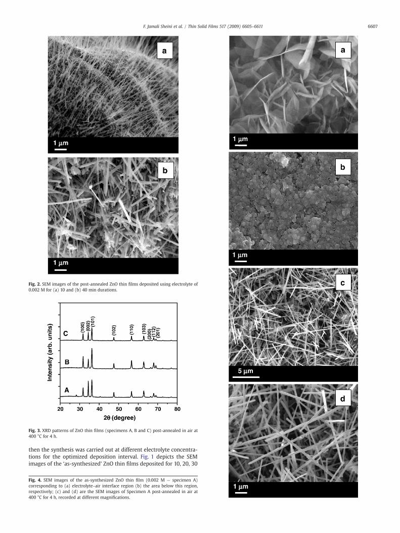
Fig. 3. XRD patterns of ZnO thin films (specimens A, B and C) post-annealed in air at400 °C for 4 h.
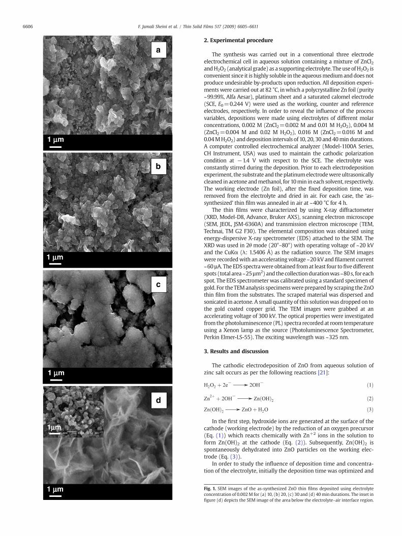
Fig. 2. SEM images of the post-annealed ZnO thin films deposited using electrolyte of0.002 M for (a) 10 and (b) 40 min durations.
6607F. Jamali Sheini et al. / Thin Solid Films 517 (2009) 6605–6611
then the synthesis was carried out at different electrolyte concentra-tions for the optimized deposition interval. Fig. 1 depicts the SEMimages of the ‘as-synthesized’ ZnO thin films deposited for 10, 20, 30
Fig. 4. SEM images of the as-synthesized ZnO thin film (0.002 M — specimen A)corresponding to (a) electrolyte–air interface region (b) the area below this region,respectively; (c) and (d) are the SEM images of Specimen A post-annealed in air at400 °C for 4 h, recorded at different magnifications.

6608 F. Jamali Sheini et al. / Thin Solid Films 517 (2009) 6605–6611
and 40 min durations, using a fixed electrolyte concentration of~0.002 M. The micrographs clearly show that the growth rate isproportional to the deposition time. The ZnO thin film, deposited for10 minute duration, shows uniform ‘granular’ morphology on theentire substrate surface. With the increase in the deposition time, thegrains were observed to agglomerate to form ‘platelet’ structures (asseen in Fig. 1(c)). For the deposition interval of 40 min, the ZnO thinfilm exhibited two distinct morphologies, the ‘2-dimensional’ (2-D)sheets randomly oriented on the area near the electrolyte–air in-terface and the ‘granular’ structures below the interface region (Fig. 1(d) and its inset). The formation of randomly oriented 2-D sheets onthe area near the interface region may be attributed to the specificgrowth mechanism. It may be speculated that, the OH− generationrate is more in the vicinity of the electrolyte–air interface regionthan elsewhere, as the interface region gets a continuous supply ofoxygen from the ambient due to continuous stirring. The more is OH−
generation rate, more is the rate of formation of ZnO particles. TheseZnO particles do not find new nucleation sites and get attached to the‘platelet’ structures. Eventually the higher surface energy of the‘platelet’ leads to its curling, thereby forming ‘2-D sheet’ havingrandom orientation.
Upon annealing in air at ~400 °C for 4 h, interestingly, all the filmsexhibited formation of ZnO wires on the entire substrate surface,irrespective of the initial morphology. The typical ‘post-annealed’ SEMimages corresponding to 10 and 40 min deposition duration areshown in Fig. 2. The density of ZnO wires is seen to be higher in the40 min case as compared to the 10 min case, which is attributed tothe higher growth rate. L. Zhang et al. have reported formation ofnanowires upon annealing the electrochemically synthesized ZnOthin film on conducting glass substrate [32]. Although the authorsclaim formation of nanowires, a careful observation of the SEM imagesreveals the presence of ‘2-D nanosheets’ along with a few nanowires.Also the aspect ratio of these nanowires is less than that obtained inthe present case. Evolution of various morphologies of electrodepos-ited zinc metal films on indium–tin oxide coated glass substrates,subjected to annealing in air at different temperatures, has beenrecently reported by G. Zou et al. [31]. It is interesting to note that theauthors have not observed formation of nanowires upon annealing.The formation ZnO wires with high density and higher aspect ratio, inthe present case, is a noticeable achievement.
The XRD patterns of ‘as-synthesized’ and ‘annealed’ ZnO thin filmsconfirm the formation of polycrystalline ZnO under the experimentalconditions mentioned above. The overall features of the diffractionpatterns do not show anymarked dependence on the deposition time.However, the intensities of the diffractions peaks are found to behigher in case of the ‘annealed’ films synthesized with larger de-position duration. The SEM and XRD results suggest the depositiontime of 40 min duration as the optimized time to get the desiredgrowth rate and the morphology of the ZnO thin films. Therefore,while investigating the effect of electrolyte concentration, the filmswere synthesized for the fixed duration of 40 min. Hereafter thespecimens A, B and C are referred to as those synthesized using theelectrolyte concentrations of 0.002 M, 0.004 M and 0.016 M, re-spectively, each deposited at 82 °C for 40 min duration.
The XRD patterns of the specimens A, B and C (annealed in air at~400 °C for 4 h) depicted in Fig. 3, exhibit a set of well defineddiffraction peaks indicating polycrystalline nature of the thin films.The diffractions peaks are indexed to the wurtzite hexagonal phase ofZnO, by comparing the observed d-values with the standard JCPDSdata [33]. The XRD patterns of the as-synthesized specimens (beforeannealing) were found to be identical to those depicted in Fig. 3,
Fig. 5. SEM images of the as-synthesized ZnO thin film (0.004 M — specimen B)corresponding to (a) electrolyte–air interface region (b) the area below this region,respectively; (c) and (d) are the SEM images of Specimen B post-annealed in air at400 °C for 4 h, recorded at different magnifications.
6609F. Jamali Sheini et al. / Thin Solid Films 517 (2009) 6605–6611
except that the intensities of the diffraction peaks were less than thoseof the post-annealed case. We have not observed any diffraction peakscorresponding to Zn (OH)2 phase, indicating the formation ofexclusively the ZnO phase under the experimental conditions.
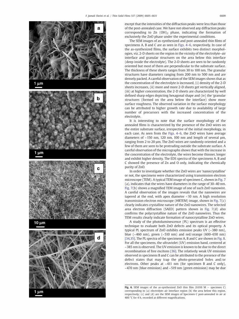
The SEM images of as-synthesized and post-annealed thin films ofspecimens A, B and C are as seen in Figs. 4–6, respectively. In case ofthe as-synthesized films, the surface exhibits two distinct morphol-ogies, viz. 2-D sheets on the region in the vicinity of the electrolyte–airinterface and granular structures on the area below this interface(deep inside the electrolyte). The 2-D sheets are seen to be randomlyoriented but most of them are perpendicular to the substrate surface.The thickness of these sheets ranges from 30 to 100 nm. The granularstructures have diameters ranging from 200 nm to 500 nm and aredensely packed. A careful observation of the SEM images shows that asthe concentration of the electrolyte is increased, (i) density of the 2-Dsheets increases, (ii) more and more 2-D sheets get vertically aligned,(iii) at higher concentration, the 2-D sheets are characterized by welldefined sharp edges depicting hexagonal shape and (iv) the ‘granularstructures (formed on the area below the interface) show moresurface roughness. The observed variation in the surface morphologycan be attributed to higher growth rate due to availability of largenumber of precursors with the increased concentration of theelectrolyte.
It is interesting to note that the surface morphology of theannealed films is characterized by the presence of the ZnO wires onthe entire substrate surface, irrespective of the initial morphology, ineach case. As seen from the Figs. 4–6, the ZnO wires have averagediameters of ~150 nm, 120 nm, 100 nm and length of several µm,ranging from 2 to 20 µm. The ZnO wires are randomly oriented and afew of them are seen to be protruding outside the substrate surface. Acareful observation of themicrographs shows that with the increase inthe concentration of the electrolyte, the wires become thinner, longerand exhibit higher density. The EDS spectra of the specimens A, B andC showed the presence of Zn and O only, indicating the chemicallypurity of ZnO.
In order to investigate whether the ZnO wires are ‘nanocrystalline’or not, the specimens were characterized using transmission electronmicroscope (TEM). A typical TEM image of specimen C, shown in Fig. 7(a), indicates that the wires have diameters in the range of 30–40 nm.Fig. 7(b) shows a magnified TEM image of one of such ZnO nanowire.A careful observation of the images reveals that the nanowires aretapered at the end, with apex diameter b10 nm. A high resolutiontransmission electron microscope (HRTEM) image, shown in Fig. 7(c)clearly indicates crystalline nature of the ZnO nanowires. The selectedarea electron diffraction (SAED) pattern shown in Fig. 7(d) alsoconfirms the polycrystalline nature of the ZnO nanowires. Thus theTEM results clearly indicate formation of nanocrystalline ZnO wires.
A study of the photoluminescence (PL) spectrum is an effectivetechnique to evaluate both ZnO defects and its optical property. Atypical PL spectrum of ZnO exhibits emission peaks UV (~380 nm),blue (~460 nm), green (~510 nm) and red/orange (600–650 nm)[34,35]. The PL spectra of the specimens A, B and C are shown in Fig. 8.For all the specimens, the ultraviolet (UV) emission band, centered at~385 nm is observed. The UV emission is known to be due to the directrecombination of free excitons [36]. The relatively weak UV emissionobserved in specimens B and C can be attributed to the presence of thedefect states that may trap the photo-generated holes and/orelectrons. Other peaks at ~411 nm (for specimen B and C only),~470 nm (blue emission) and ~519 nm (green emission) may be due
Fig. 6. SEM images of the as-synthesized ZnO thin film (0.016 M — specimen C)corresponding to (a) electrolyte–air interface region (b) the area below this region,respectively; (c) and (d) are the SEM images of Specimen C post-annealed in air at400 °C for 4 h, recorded at different magnifications.
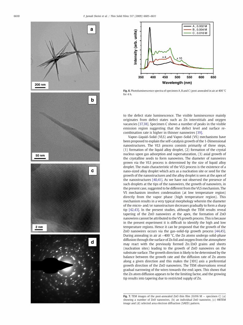
Fig. 8. Photoluminescence spectra of specimen A, B and C (post-annealed in air at 400 °Cfor 4 h.
6610 F. Jamali Sheini et al. / Thin Solid Films 517 (2009) 6605–6611
to the defect state luminescence. The visible luminescence mainlyoriginates from defect states such as Zn interstitials and oxygenvacancies [37,38]. Specimen C shows a number of peaks in the visibleemission region suggesting that the defect level and surface re-combination rate is higher in thinner nanowires [39].
Vapor–Liquid–Solid (VLS) and Vapor–Solid (VS) mechanisms havebeenproposed to explain the self-catalysis growth of the 1-Dimensionalnanostructures. The VLS process consists primarily of three steps,(1) formation of the liquid alloy droplet, (2) formation of the crystalnucleus upon gas adsorption and supersaturation, (3) axial growth ofthe crystalline seeds to form nanowires. The diameter of nanowiresgrown via the VLS process is determined by the size of liquid alloydroplet. The main characteristic of the VLS process is the existence of anano-sized alloy droplet which acts as a nucleation site or seed for thegrowth of the nanostructures and the alloy droplet is seen at the apex ofthe nanostructures [40,41]. As we have not observed the presence ofsuch droplets at the tips of the nanowires, the growth of nanowires, inthe present case, suggested to be different from theVLSmechanism. TheVS mechanism involves condensation (at low temperature region)directly from the vapor phase (high temperature region). Thismechanism results in a very typical morphology wherein the diameterof the micro- and/or nanostructure decreases gradually to form a sharptip [42,43]. In the present studies, although the TEM results revealtapering of the ZnO nanowires at the apex, the formation of ZnOnanowires cannot beattributed to theVSgrowthprocess. This is becausein the present experiment it is difficult to identify the high and lowtemperature regions. Hence it can be proposed that the growth of theZnO nanowires occurs via the gas–solid-tip growth process [44,45].During annealing in air at ~400 °C, the Zn atoms undergo solid-phasediffusion through the surface of Zn foil and oxygen from the atmospheremay react with the previously formed Zn/ZnO grains and sheets(nucleation sites) leading to the growth of ZnO nanowires on thesubstrate surface. The growth direction is likely to be determined by thebalance between the growth rate and the diffusion rate of Zn atomsalong a given direction and this makes the [101] axis a preferentialgrowth direction of the ZnO nanowires. The TEM observations revealgradual narrowing of the wires towards the end/apex. This shows thatthe Zn atom diffusion appears to be the limiting factor, and the growingtip results into tapering due to restricted supply of Zn.
Fig. 7. TEM images of the post-annealed ZnO thin film (0.016 M — specimen C) (a)showing a number of ZnO nanowires, (b) an individual ZnO nanowire, (c) HRTEMimage and (d) selected area electron diffraction (SAED) pattern.

6611F. Jamali Sheini et al. / Thin Solid Films 517 (2009) 6605–6611
4. Conclusions
Nanocrystalline ZnO thin films have been synthesized by cathodicelectrodeposition from aqueous solution on Zinc substrate. The XRDpatterns show that the ‘as-synthesized’ and ‘post-annealed’ ZnO filmsposses a hexagonal wurtzite structure. The surface morphology of theas-synthesized ZnO thin film is found to be influenced by theelectrolyte concentration and deposition duration. The ‘as-synthe-sized’ ZnO thin films, prepared under the optimized conditions, showtwo distinct type of morphology, characterized by ‘2-D nanosheets’and ‘granular nanostructures’ in the regions near the electrolyte–airinterface and below it, respectively. Annealing of the thin films in airresults in the formation of ZnO nanowires of high density and highaspect ratio. The SEM and TEM analysis reveal that the ZnO wires arenanocrystalline in nature having average length ranging from 2 to20 µm and diameter in the range of 30–40 nm.
Acknowledgements
F. Jamali Sheini would like to thank Islamic Azad University, AhwazBranch, Iran, for the award of Research Fellowship. MAMwould like tothank University of Pune, for the financial support via the researchgrant RG-3/Physics, 2007.
References
[1] Y. Zhang, K. Yu, S. Ouyang, Z. Zhu, Physica B 382 (2006) 76.[2] Y. Huang, K. Yu, Z. Zhu, Curr. Appl. Phys. 7 (2007) 702.[3] L. Wei, X. Zhang, Z. Zuoya, J. Vac. Sci. Technol. B 25 (2007) 608.[4] R. Könenkamp, R.C. Word, C. Schlegel, Appl. Phys. Lett. 85 (2004) 6004.[5] X.Y. Kong, Y. Ding, R. Yang, Z.L. Wang, Science 303 (2004) 1348.[6] B.P. Zhang, N.T. Binh, K. Wakatsuki, Y. Segawa, Y. Yamada, N. Usami, M. Kawasaki,
H. Koinuma, Appl. Phys. Lett. 84 (2004) 4098.[7] S.K. Marathe, P.M. Koinkar, S.S. Ashtaputre, M.A. More, S.W. Gosavi, D.S. Joag,
S.K. Kulkarni, Nanotechnology 17 (2006) 1932.[8] A. Umar, Y.B. Hahn, Appl. Phys. Lett. 88 (2006) 173120.
[9] J. Xiao, X. Zhang, G. Zhang, Nanotechnology 19 (2008) 295706.[10] A. Umar, Y.B. Hahn, Cryst. Growth Des. 8 (2008) 2741.[11] Y. Wu, Z. Xi, G. Zhang, J. Zhang, D. Guo, Cryst. Growth Des. 8 (2008) 2646.[12] A. Umar, B. Karunagaran, S.H. Kim, E.-K. Suh, Y.B. Hahn, Inorg. Chem. 47 (2008) 4088.[13] A. Umar, S.H. Kim, E.-K. Suh, Y.B. Hahn, Chem. Phys. Lett. 440 (2007) 110.[14] A. Umar, M.M. Rahman, S.H. Kim, Y.B. Hahn, Chem. Commun. (2008) 166.[15] A. Umar, E.-K. Suh, Y.B. Hahn, J. Phys. D: Appl. Phys. 40 (2007) 3478.[16] A. Umar, S.H. Kim, H. Lee, N. Lee, Y.B. Hahn, J. Phys. D: Appl. Phys. 41 (2008) 065412.[17] A. Umar, Y.B. Hahn, Appl. Surf. Sci. 254 (2008) 3339.[18] Y. Zhang, R.E. Russo, S.S. Mao, Appl. Phys. Lett. 87 (2005) 133115.[19] R.F. Zhuo, H.T. Feng, J.T. Chen, D. Yan, J.J. Feng, H.J. Li, B.S. Geng, S. Cheng, X.Y. Xu,
P.X. Yan, J. Phys. Chem. C 112 (2008) 11767.[20] C.X. Shan, Z. Liu, Z.Z. Zhang, D.Z. Shen, S.K. Hark, J. Phys. Chem. B 110 (2006) 11176.[21] Y. Chen, H.-J. Ko, S.K. Hong, T. Yao, Appl. Phys. Lett. 76 (2000) 559.[22] S.-H. Jung, E. Oh, K.H. Lee, Y. Yang, C.G. Park, W. Park, S.H. Jeong, Cryst. Growth Des.
8 (2008) 265.[23] S. Peulon, D. Lincot, Adv. Mater. 8 (1996) 166.[24] Th. Pauporte, D. Lincot, Appl. Phys. Lett. 75 (1999) 3817.[25] B. Canava, D. Lincot, J. Appl. Electrochem. 30 (2000) 711.[26] Th. Pauporte, D. Lincot, J. Electrochem. Soc. 145 (2001) 864.[27] M. Izaki, T. Omi, Appl. Phys. Lett. 68 (1996) 2439.[28] Th. Pauporte, D. Lincot, J. Electrochem. Soc. 148 (2001) C310.[29] J. Lee, Y. Tak, Electrochem. Solid State Lett. 4 (2001) C63.[30] D. Gal, G. Hodes, D. Lincot, H.-W. Schock, Thin Solid Films 361–362 (2000) 79.[31] G. Zou, W. Chen, R. Liu, Z. Xu, Mater. Lett. 61 (2007) 4305.[32] L. Zhang, Z. Chen, Y. Tang, Z. Jia, Thin Solid Films 492 (2005) 24.[33] Powder Diffraction File, International Centre for Diffraction Data, Swarthmore, PA,
JCPDS File No. 80-0075, 1999.[34] S. Fujihara, Y. Ogawa, A. Kasai, Chem. Mater. 16 (2004) 2965.[35] X. Liu, X. Wu, H. Cao, R.P.H. Chang, J. Appl. Phys. 95 (2004) 3141.[36] Y.C. Kong, D.P. Yu, B. Zhang, W. Fang, S.Q. Feng, Appl. Phys. Lett. 78 (2001) 407.[37] K. Vanheusden, C.H. Seager,W.L. Warren, D.R. Tallant, J.A. Voigt, Appl. Phys. Lett. 68
(1996) 403.[38] B. Lin, Z. Fu, Y. Jia, Appl. Phys. Lett. 79 (2001) 943.[39] I. Shalish, H. Temkin, V. Narayanamurti, Phys. Rev. B. 69 (2004) 245401.[40] R.S. Wagner, W.C. Ellis, Appl. Phys. Lett. 4 (1964) 89.[41] P.X. Gao, Y. Ding, Z.L. Wang, Nano Lett. 3 (2003) 1315.[42] A. Umar, S.H. Kim, Y.-S. Lee, K.S. Nahm, Y.B. Hahn, J. Cryst. Growth 282 (2005) 131.[43] Y. Zhang, H. Jia, X. Luo, X. Chen, D. Yu, R. Wang, J. Phys. Chem. B 107 (2003) 8289.[44] H.Y. Dang, J. Wang, S.S. Fan, Nanotechnology 14 (2003) 738.[45] X. Wen, Y. Fang, Q. Pang, C. Yang, J. Wang, W. Ge, K.S. Wong, S. Yang, Phys. Chem. B
109 (2005) 15303.