Preferred growth orientation of metallic fcc nanowires under direct and alternating...
8
IOP PUBLISHING NANOTECHNOLOGY Nanotechnology 18 (2007) 135709 (8pp) doi:10.1088/0957-4484/18/13/135709 Preferred growth orientation of metallic fcc nanowires under direct and alternating electrodeposition conditions Florian Maurer 1 , Joachim Br¨ otz 1,5 , Shafqat Karim 2,3 , Maria Eugenia Toimil Molares 4 , Christina Trautmann 4 and Hartmut Fuess 1 1 Institute of Materials and Earth Sciences, Darmstadt University of Technology, Petersenstraße 23, D-64287 Darmstadt, Germany 2 Department of Chemistry, University of Marburg, Hans-Meerwein-Straße, D-35032 Marburg, Germany 3 Department of Physics, CIIT, Islamabad, Pakistan 4 Gesellschaft f¨ ur Schwerionenforschung (GSI), Planckstraße 1, D-64291 Darmstadt, Germany E-mail: [email protected] Received 27 November 2006, in final form 10 January 2007 Published 28 February 2007 Online at stacks.iop.org/Nano/18/135709 Abstract Gold and copper nanowires were generated through electrochemical deposition into nanoporous polymeric templates. Depending on the growth conditions, such wires exhibited a distinct textured structure as evidenced by x-ray diffraction. The preferred growth orientation is explained by applying the broken-bond model in combination with surface-energy anisotropy and energy minimization. During the growth process, the aspect ratio of the cylindrical nanowire and thus the area of the mantle surface and its contribution to the total surface energy increase. Under direct current deposition conditions, 110 textured metallic fcc nanowires represent the configuration of lowest surface energy at aspect ratios above 1. Under alternating current deposition conditions, {110} nanowire base surfaces vanish due to their high surface energy, leading to successive development of a 100 texture as the configuration of lowest energy at aspect ratios above 5. (Some figures in this article are in colour only in the electronic version) 1. Introduction The ever-increasing quest for the miniaturization of electronic devices is one of the driving forces for improvement and control of the fabrication of nanostructures. Research activities exploring new material properties ascribed to the small size of nanostructures have increased enormously within the last decade. In this study we are interested in the fabrication and structural properties of one-dimensional face-centred cubic (fcc) metallic nanowires. A common production technique for nanowires is based on the electrochemical deposition of metals into pores of constrained geometry. 5 Author to whom any correspondence should be addressed. Suitable nanopores are available in templates of anodized aluminium oxide [1–3] or polymer membranes with etched ion tracks [3–8]. The electrodeposition process is influenced by numerous parameters, e.g. overvoltage, temperature, pH value and composition of the electrolyte solution, and has been investigated for many different systems [9–11, 14]. Our studies focus on the development of the crystallographic texture of template-grown fcc nanowires as a function of the overvoltage. We produced gold and copper nanowire ensembles by electrochemically filling the pores of etched ion-track membranes. We investigated the texture of the wires by x-ray diffraction (XRD). In recent years, nanowires electrochemically grown under direct current conditions in pores with diameters smaller than 100 nm have been found 0957-4484/07/135709+08$30.00 1 © 2007 IOP Publishing Ltd Printed in the UK
-
Upload
independent -
Category
Documents
-
view
3 -
download
0
Transcript of Preferred growth orientation of metallic fcc nanowires under direct and alternating...

IOP PUBLISHING NANOTECHNOLOGY
Nanotechnology 18 (2007) 135709 (8pp) doi:10.1088/0957-4484/18/13/135709
Preferred growth orientation of metallicfcc nanowires under direct and alternatingelectrodeposition conditionsFlorian Maurer1, Joachim Brotz1,5, Shafqat Karim2,3,Maria Eugenia Toimil Molares4, Christina Trautmann4 andHartmut Fuess1
1 Institute of Materials and Earth Sciences, Darmstadt University of Technology,Petersenstraße 23, D-64287 Darmstadt, Germany2 Department of Chemistry, University of Marburg, Hans-Meerwein-Straße, D-35032Marburg, Germany3 Department of Physics, CIIT, Islamabad, Pakistan4 Gesellschaft fur Schwerionenforschung (GSI), Planckstraße 1, D-64291 Darmstadt,Germany
E-mail: [email protected]
Received 27 November 2006, in final form 10 January 2007Published 28 February 2007Online at stacks.iop.org/Nano/18/135709
AbstractGold and copper nanowires were generated through electrochemicaldeposition into nanoporous polymeric templates. Depending on the growthconditions, such wires exhibited a distinct textured structure as evidenced byx-ray diffraction. The preferred growth orientation is explained by applyingthe broken-bond model in combination with surface-energy anisotropy andenergy minimization. During the growth process, the aspect ratio of thecylindrical nanowire and thus the area of the mantle surface and itscontribution to the total surface energy increase. Under direct currentdeposition conditions, 〈110〉 textured metallic fcc nanowires represent theconfiguration of lowest surface energy at aspect ratios above 1. Underalternating current deposition conditions, {110} nanowire base surfacesvanish due to their high surface energy, leading to successive development ofa 〈100〉 texture as the configuration of lowest energy at aspect ratios above 5.
(Some figures in this article are in colour only in the electronic version)
1. Introduction
The ever-increasing quest for the miniaturization of electronicdevices is one of the driving forces for improvement andcontrol of the fabrication of nanostructures. Research activitiesexploring new material properties ascribed to the small sizeof nanostructures have increased enormously within the lastdecade. In this study we are interested in the fabricationand structural properties of one-dimensional face-centredcubic (fcc) metallic nanowires. A common productiontechnique for nanowires is based on the electrochemicaldeposition of metals into pores of constrained geometry.
5 Author to whom any correspondence should be addressed.
Suitable nanopores are available in templates of anodizedaluminium oxide [1–3] or polymer membranes with etchedion tracks [3–8]. The electrodeposition process is influencedby numerous parameters, e.g. overvoltage, temperature, pHvalue and composition of the electrolyte solution, and hasbeen investigated for many different systems [9–11, 14]. Ourstudies focus on the development of the crystallographictexture of template-grown fcc nanowires as a function ofthe overvoltage. We produced gold and copper nanowireensembles by electrochemically filling the pores of etchedion-track membranes. We investigated the texture of thewires by x-ray diffraction (XRD). In recent years, nanowireselectrochemically grown under direct current conditions inpores with diameters smaller than 100 nm have been found
0957-4484/07/135709+08$30.00 1 © 2007 IOP Publishing Ltd Printed in the UK

Nanotechnology 18 (2007) 135709 F Maurer et al
to exhibit a 〈110〉 preferred orientation, as for example in fccmetals such as nickel [15, 11], copper [6, 9], silver [11–13]and gold [16, 17]. Recently, fcc silver nanowires wereshown to establish a coexisting hexagonal phase with thehighest concentration at diameters around 30 nm [18]. Underalternating electrodeposition conditions, 〈100〉 orientationshave been demonstrated for fcc gold nanowires [16]. Alsonon-metallic nanowires show a diameter-dependent orientationeffect: silicon nanowires synthesized with the vapour–liquid–solid technique change their preferred growth orientationfrom 〈111〉 to 〈110〉 at wire diameters below approximately25 nm [19–22]. This transition is explained in terms ofthe surface and edge-tension energy which depends on thewire diameter [21] and on the diameter-dependent nucleationthermodynamics of the Au catalyst used [22]. In this paperwe apply energetic considerations to explain the preferredgrowth directions found for metallic fcc nanowires. Ourcalculations are based on the broken-bond model proposed byMackenzie et al [23] and include contributions from surface-energy anisotropy of low-index fcc surfaces and surface-energy minimizing growth tendencies. The predictions ofthese calculations are in good agreement with the experimentaldata from XRD texture analysis of gold and copper nanowireensembles presented in this paper, as well as numerousobservations for metallic fcc nanowires from the literature.
2. Experimental details
Nanoporous templates for the growth of gold and coppernanowires were produced by irradiating polycarbonate foils(MAKROFOL N, Bayer Leverkusen) of thickness 30 μm withheavy ion projectiles of energy 11.1 MeV/u. The irradiationexperiments were carried out at the UNILAC acceleratorfacility of GSI (Darmstadt, Germany) applying a fluence of109 ions cm−2. The damaged polymer material created alongthe ion trajectory was preferentially dissolved by chemicaletching, thus enlarging each ion track to a cylindrical porewith diameters of a few tens of nanometres. Prior to theetching procedure, the foils were exposed to UV light for 1 hper side to enhance the etching rate along the tracks [24, 25]and thus to produce pores of high aspect ratio (ratio of lengthover diameter). The etching was performed in 6 M NaOH at50 ◦C for between 1 and 3 min, producing pores with diametersranging between approximately 70 and 150 nm, respectively.
One side of the template was covered with a thingold layer by plasma sputtering in order to provideelectrical conductivity for the electrodeposition. This goldlayer was subsequently reinforced by an electrodepositedpolycrystalline copper layer (∼10 μm thick for gold wireensembles and ∼0.5 μm for copper wire ensembles) usinga commercial electrolyte solution (Cupatierbad, RiedelCompany). Copper wires were grown at 50 ◦C in an aqueoussolution of 238 g l−1 CuSO4·5H2O and 18 mol l−1 H2SO4 [6].Potentiostatic direct current (dc) deposition was performedat −40 mV. Potentiostatic alternating current (ac) depositionwas performed at −80 mV for 1 s and +20 mV for 0.1 s.Gold nanowires were deposited at 65 ◦C from a commercialgold bath containing potassium dicyanoaurate(I) (Puramet402, Doduco Company). Potentiostatic dc deposition wasaccomplished at −1.2 V. Potentiostatic ac deposition was
performed at −1.3 V for 6 s and +0.4 mV for 1 s using thesame electrolyte solution [16]. The texture of the different wireensembles embedded in the polymer matrix was investigatedby XRD using a STOE four-circle diffractometer with Co Kα
radiation.
3. Results
3.1. XRD
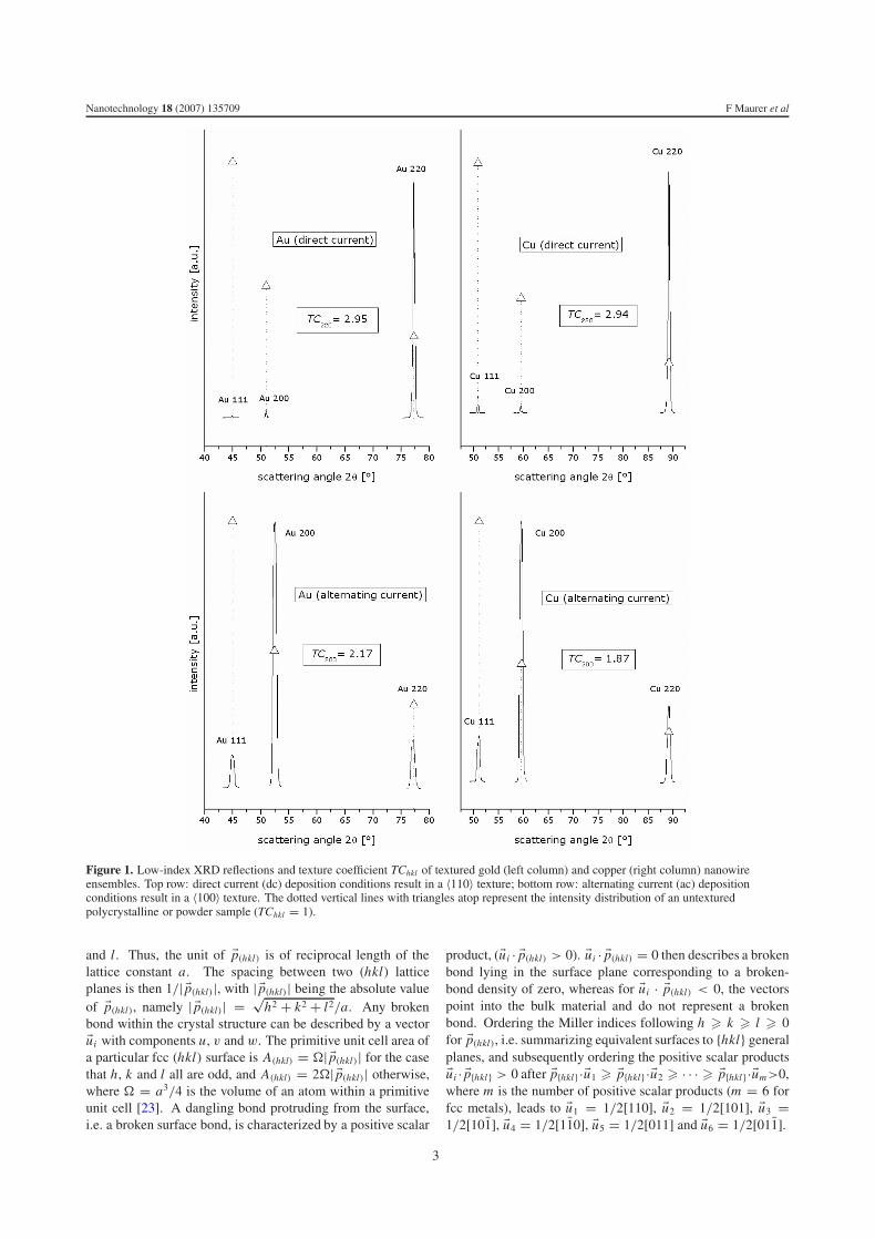
The x-ray diffractograms of the copper and gold nanowireensembles electrodeposited under dc and ac conditions areshown in figure 1. The texture coefficients TChkl of the hklreflections of highest intensity were calculated for the fourdifferent samples taking into consideration the intensities ofthe first three reflections, i.e. 111, 200 and 220. In the caseof potentiostatic dc deposition (figure 1, top row) the highintensity of the 220 reflections shows that for both metalsthe wires develop a strong preferred orientation in the 〈110〉direction. The texture coefficient TC220 of the gold sample was2.95 and of the copper sample 2.94. The maximum value ofthe texture coefficients was 3, corresponding to a sample withall crystals oriented in the same direction. In a sample withrandomly oriented lattice planes (untextured polycrystal orpowder sample) the intensity of the 220 reflection compared tothe intensity of the 111 reflection is 32% and 20% for gold andcopper, respectively, giving a texture coefficient TC220 = 1.The dotted vertical lines with triangles atop index the intensitydistribution of an untextured fcc polycrystalline or powdersample.
In contrast, in the case of wires deposited underpotentiostatic ac conditions, the high intensity of the 200reflections show that wires develop a preferred orientation inthe 〈100〉 direction with texture coefficients of TC200 = 2.17for gold and TC200 = 1.87 for copper. For comparison, theintensities of an untextured polycrystalline or powder sample(TC200 = 1) are embedded as dotted vertical lines withtriangles atop. For both gold and copper, the 〈110〉 textureunder dc deposition is stronger (TC220 ≈ 2.95 for bothelements) than the 〈100〉 texture under ac conditions (TC200
is 2.17 for gold and 1.87 for copper, respectively).
3.2. Model calculations: broken-bond model
Assuming perfectly flat and atomically smooth surfaces, theenergy of any arbitrary fcc surface can be derived using thebroken-bond model, where broken bonds represent missingneighbours of atoms located on a particular surface [23].The energy necessary to create a surface is considered to beproportional to the number of broken bonds [26–28]. For fccmetals it is reasonable to consider only the contribution ofnearest neighbours to the surface energy as the contributionof second-nearest-neighbour bonds is only a few per cent andthus negligible [26]. In a monoatomic fcc crystal, each atom issurrounded by 12 nearest neighbours at a distance of
√2a/2,
a being the lattice constant of the unit cell. The positionsof the 12 nearest-neighbour atoms are described by the 121/2〈110〉 vectors. A particular (hkl) lattice plane, with h, kand l being the Miller indices, i.e. the least common multipleof the reciprocal intersection points with the crystal axes, isdescribed by its normal vector �p(hkl) with components h, k
2
Nanotechnology 18 (2007) 135709 F Maurer et al
Figure 1. Low-index XRD reflections and texture coefficient TChkl of textured gold (left column) and copper (right column) nanowireensembles. Top row: direct current (dc) deposition conditions result in a 〈110〉 texture; bottom row: alternating current (ac) depositionconditions result in a 〈100〉 texture. The dotted vertical lines with triangles atop represent the intensity distribution of an untexturedpolycrystalline or powder sample (TChkl = 1).
and l . Thus, the unit of �p(hkl) is of reciprocal length of thelattice constant a. The spacing between two (hkl) latticeplanes is then 1/| �p(hkl)|, with | �p(hkl)| being the absolute valueof �p(hkl), namely | �p(hkl)| = √
h2 + k2 + l2/a. Any brokenbond within the crystal structure can be described by a vector�ui with components u, v and w. The primitive unit cell area ofa particular fcc (hkl) surface is A(hkl) = �| �p(hkl)| for the casethat h, k and l all are odd, and A(hkl) = 2�| �p(hkl)| otherwise,where � = a3/4 is the volume of an atom within a primitiveunit cell [23]. A dangling bond protruding from the surface,i.e. a broken surface bond, is characterized by a positive scalar
product, (�ui · �p(hkl) > 0). �ui · �p(hkl) = 0 then describes a brokenbond lying in the surface plane corresponding to a broken-bond density of zero, whereas for �ui · �p(hkl) < 0, the vectorspoint into the bulk material and do not represent a brokenbond. Ordering the Miller indices following h � k � l � 0for �p(hkl), i.e. summarizing equivalent surfaces to {hkl} generalplanes, and subsequently ordering the positive scalar products�ui · �p{hkl } > 0 after �p{hkl} · �u1 � �p{hkl} · �u2 � · · · � �p{hkl}· �um>0,where m is the number of positive scalar products (m = 6 forfcc metals), leads to �u1 = 1/2[110], �u2 = 1/2[101], �u3 =1/2[101], �u4 = 1/2[110], �u5 = 1/2[011] and �u6 = 1/2[011].
3
Nanotechnology 18 (2007) 135709 F Maurer et al
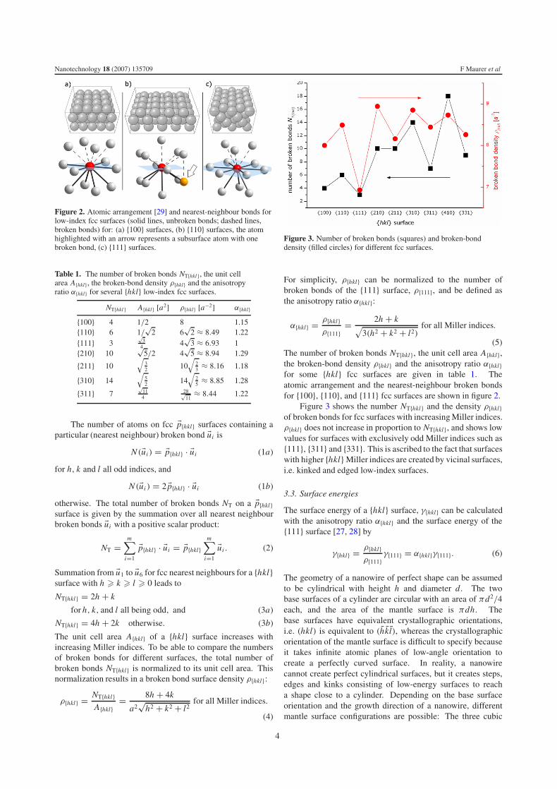
Figure 2. Atomic arrangement [29] and nearest-neighbour bonds forlow-index fcc surfaces (solid lines, unbroken bonds; dashed lines,broken bonds) for: (a) {100} surfaces, (b) {110} surfaces, the atomhighlighted with an arrow represents a subsurface atom with onebroken bond, (c) {111} surfaces.
Table 1. The number of broken bonds NT{hkl }, the unit cellarea A{hkl}, the broken-bond density ρ{hkl} and the anisotropyratio α{hkl} for several {hkl} low-index fcc surfaces.
NT{hkl } A{hkl} [a2] ρ{hkl} [a−2] α{hkl}
{100} 4 1/2 8 1.15{110} 6 1/
√2 6
√2 ≈ 8.49 1.22
{111} 3√
34 4
√3 ≈ 6.93 1
{210} 10√
5/2 4√
5 ≈ 8.94 1.29
{211} 10√
32 10
√23 ≈ 8.16 1.18
{310} 14√
52 14
√25 ≈ 8.85 1.28
{311} 7√
114
28√11
≈ 8.44 1.22
The number of atoms on fcc �p{hkl} surfaces containing aparticular (nearest neighbour) broken bond �ui is
N(�ui ) = �p{hkl} · �ui (1a)
for h, k and l all odd indices, and
N(�ui ) = 2 �p{hkl} · �ui (1b)
otherwise. The total number of broken bonds NT on a �p{hkl}surface is given by the summation over all nearest neighbourbroken bonds �ui with a positive scalar product:
NT =m∑
i=1
�p{hkl} · �ui = �p{hkl}m∑
i=1
�ui . (2)
Summation from �u1 to �u6 for fcc nearest neighbours for a {hkl}surface with h � k � l � 0 leads to
NT{hkl } = 2h + k
for h, k, and l all being odd, and (3a)
NT{hkl } = 4h + 2k otherwise. (3b)
The unit cell area A{hkl} of a {hkl} surface increases withincreasing Miller indices. To be able to compare the numbersof broken bonds for different surfaces, the total number ofbroken bonds NT{hkl} is normalized to its unit cell area. Thisnormalization results in a broken bond surface density ρ{hkl}:
ρ{hkl} = NT{hkl }A{hkl}
= 8h + 4k
a2√
h2 + k2 + l2for all Miller indices.
(4)
Figure 3. Number of broken bonds (squares) and broken-bonddensity (filled circles) for different fcc surfaces.
For simplicity, ρ{hkl} can be normalized to the number ofbroken bonds of the {111} surface, ρ{111}, and be defined asthe anisotropy ratio α{hkl}:
α{hkl} = ρ{hkl}ρ{111}
= 2h + k√3(h2 + k2 + l2)
for all Miller indices.
(5)The number of broken bonds NT{hkl }, the unit cell area A{hkl},the broken-bond density ρ{hkl} and the anisotropy ratio α{hkl}for some {hkl} fcc surfaces are given in table 1. Theatomic arrangement and the nearest-neighbour broken bondsfor {100}, {110}, and {111} fcc surfaces are shown in figure 2.
Figure 3 shows the number NT{hkl } and the density ρ{hkl}of broken bonds for fcc surfaces with increasing Miller indices.ρ{hkl} does not increase in proportion to NT{hkl }, and shows lowvalues for surfaces with exclusively odd Miller indices such as{111}, {311} and {331}. This is ascribed to the fact that surfaceswith higher {hkl} Miller indices are created by vicinal surfaces,i.e. kinked and edged low-index surfaces.
3.3. Surface energies
The surface energy of a {hkl} surface, γ{hkl} can be calculatedwith the anisotropy ratio α{hkl} and the surface energy of the{111} surface [27, 28] by
γ{hkl} = ρ{hkl}ρ{111}
γ{111} = α{hkl}γ{111}. (6)
The geometry of a nanowire of perfect shape can be assumedto be cylindrical with height h and diameter d. The twobase surfaces of a cylinder are circular with an area of πd2/4each, and the area of the mantle surface is πdh. Thebase surfaces have equivalent crystallographic orientations,i.e. (hkl) is equivalent to (hkl), whereas the crystallographicorientation of the mantle surface is difficult to specify becauseit takes infinite atomic planes of low-angle orientation tocreate a perfectly curved surface. In reality, a nanowirecannot create perfect cylindrical surfaces, but it creates steps,edges and kinks consisting of low-energy surfaces to reacha shape close to a cylinder. Depending on the base surfaceorientation and the growth direction of a nanowire, differentmantle surface configurations are possible: The three cubic
4

Nanotechnology 18 (2007) 135709 F Maurer et al
Figure 4. Stereographic projections of low-index cubic crystals: (a) [001] orientation, (b) [011] orientation, (c) [111] orientation.
Table 2. Broken-bond density ρ of {hkl} low-index mantle surfaces for 〈100〉, 〈110〉 and 〈111〉 oriented fcc nanowires.
〈100〉 〈110〉 〈111〉ρ{hkl} [a−2] Percentage (%) ρ{hkl} [a−2] Percentage (%) ρ{hkl} [a−2] Percentage (%)
{100} 8 50 {111} 6.93 50 {110} 8.49 50{110} 8.46 50 {100} 8 30 {211} 8.16 50
{110} 8.46 20
low-index surfaces {100}, {110} and {111} exhibit differentcrystallographic symmetries: {100} surfaces are characterizedby a fourfold symmetry (figure 4(a)), {110} by a twofoldsymmetry (figure 4(b)) and {111} surfaces by a threefoldsymmetry (figure 4(c)).
The contribution of each particular low-index surface tothe mantle is given by the amount of the whole nanowiremantle area it occupies, which is equivalent to the proportionof the circumference of a circle: a nanowire oriented inthe 〈100〉 direction (figure 4(a)) is surrounded by {100} and{110} surfaces aligned in 45◦ angles, each covering half ofthe mantle area. A nanowire oriented in the 〈110〉 direction(figure 4(b)) is surrounded by {111}, {110} and {100} surfacesaligned in 54.74◦ and 35.26◦ steps. {111} surfaces then coverhalf of the mantle area, {110} approximately 20% and {100}approximately 30%, respectively. A nanowire oriented in the〈111〉 direction (figure 4(c)) is surrounded by {110} and {211}surfaces aligned in 30◦ angles, each again covering half of themantle area. Independent of the nanowire diameter and thenumber of steps, edges and kinks of the mantle surface, thebase surfaces are always surrounded by the same particularlow-index planes, and the ratio of each surface to the wholemantle area does not change. The total surface energy, Etotal,of a nanowire can then be calculated by
Etotal = Emantle + Etop + Ebottom = γmantle Amantle + 2γbase Abase
(7)where Ebase and Etop are the energetic contributions of thebase and the top surfaces, and Emantle is the contribution of themantle surface. The low-index fcc mantle surfaces surrounding〈100〉, 〈110〉 and 〈111〉 oriented nanowires (figure 4) are listedin table 2.
The particular total surface energy, Etotal, consistingof different low-index surfaces, can be calculated withequation (7) using the broken-bond density ρ{hkl} and takinginto account the different ratios of the different surfaces to thetotal surface area. The surface energy E〈hkl〉 of a cylindricalnanowire with a specific 〈hkl〉 growth orientation is given by
E〈100〉 = πd2
2γ{100} + πdh(0.5γ{100} + 0.5γ{110}) (8a)
Figure 5. Evolution of the normalized total surface energy ofnanowires of different growth directions as a function of the aspectratio (length h to diameter d); the dimensions and intersection pointsare not to scale: solid curve, 〈100〉 orientation; dotted curve, 〈110〉orientation; dashed curve, 〈111〉 orientation; E〈110〉 = E〈100〉 at anaspect ratio of 0.36; E〈110〉 = E〈111〉 at an aspect ratio of 1;E〈100〉 = E〈111〉 at an aspect ratio of 5.
E〈110〉 = πd2
2γ{110} + πdh(0.5γ{111} + 0.2γ{110} + 0.3γ{100})
(8b)
E〈111〉 = πd2
2γ{111} + πdh(0.5γ{110} + 0.5γ{211}). (8c)
The evolution of E〈hkl〉 during the nanowire growthprocess is shown as a function of the aspect ratio h/d ofa nanowire in figure 5 for 〈100〉, 〈110〉 and 〈111〉 growthdirections. For simplicity, all total surface energies arenormalized to the surface energy γ{111}, thus enabling theapplication of the anisotropy ratio α{hkl} (equation (6)).
During the growth process of any nanowire, the aspectratio increases and its surface area gets larger, thus increasingthe surface energy. The gain in surface energy is not the samefor the different orientations (see equations (8a)–(8c)). Severalregions can be defined on the basis of the different slopes: up to
5
Nanotechnology 18 (2007) 135709 F Maurer et al
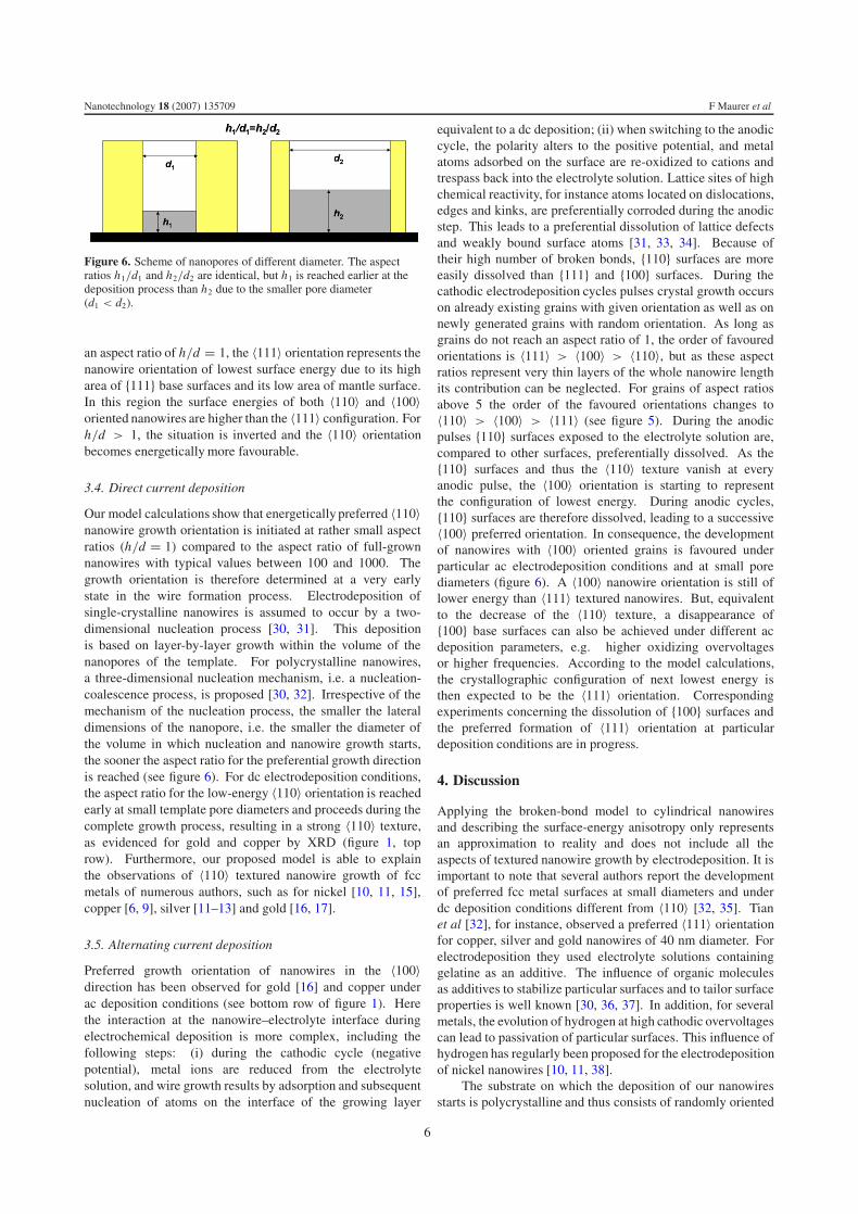
Figure 6. Scheme of nanopores of different diameter. The aspectratios h1/d1 and h2/d2 are identical, but h1 is reached earlier at thedeposition process than h2 due to the smaller pore diameter(d1 < d2).
an aspect ratio of h/d = 1, the 〈111〉 orientation represents thenanowire orientation of lowest surface energy due to its higharea of {111} base surfaces and its low area of mantle surface.In this region the surface energies of both 〈110〉 and 〈100〉oriented nanowires are higher than the 〈111〉 configuration. Forh/d > 1, the situation is inverted and the 〈110〉 orientationbecomes energetically more favourable.
3.4. Direct current deposition
Our model calculations show that energetically preferred 〈110〉nanowire growth orientation is initiated at rather small aspectratios (h/d = 1) compared to the aspect ratio of full-grownnanowires with typical values between 100 and 1000. Thegrowth orientation is therefore determined at a very earlystate in the wire formation process. Electrodeposition ofsingle-crystalline nanowires is assumed to occur by a two-dimensional nucleation process [30, 31]. This depositionis based on layer-by-layer growth within the volume of thenanopores of the template. For polycrystalline nanowires,a three-dimensional nucleation mechanism, i.e. a nucleation-coalescence process, is proposed [30, 32]. Irrespective of themechanism of the nucleation process, the smaller the lateraldimensions of the nanopore, i.e. the smaller the diameter ofthe volume in which nucleation and nanowire growth starts,the sooner the aspect ratio for the preferential growth directionis reached (see figure 6). For dc electrodeposition conditions,the aspect ratio for the low-energy 〈110〉 orientation is reachedearly at small template pore diameters and proceeds during thecomplete growth process, resulting in a strong 〈110〉 texture,as evidenced for gold and copper by XRD (figure 1, toprow). Furthermore, our proposed model is able to explainthe observations of 〈110〉 textured nanowire growth of fccmetals of numerous authors, such as for nickel [10, 11, 15],copper [6, 9], silver [11–13] and gold [16, 17].
3.5. Alternating current deposition
Preferred growth orientation of nanowires in the 〈100〉direction has been observed for gold [16] and copper underac deposition conditions (see bottom row of figure 1). Herethe interaction at the nanowire–electrolyte interface duringelectrochemical deposition is more complex, including thefollowing steps: (i) during the cathodic cycle (negativepotential), metal ions are reduced from the electrolytesolution, and wire growth results by adsorption and subsequentnucleation of atoms on the interface of the growing layer
equivalent to a dc deposition; (ii) when switching to the anodiccycle, the polarity alters to the positive potential, and metalatoms adsorbed on the surface are re-oxidized to cations andtrespass back into the electrolyte solution. Lattice sites of highchemical reactivity, for instance atoms located on dislocations,edges and kinks, are preferentially corroded during the anodicstep. This leads to a preferential dissolution of lattice defectsand weakly bound surface atoms [31, 33, 34]. Because oftheir high number of broken bonds, {110} surfaces are moreeasily dissolved than {111} and {100} surfaces. During thecathodic electrodeposition cycles pulses crystal growth occurson already existing grains with given orientation as well as onnewly generated grains with random orientation. As long asgrains do not reach an aspect ratio of 1, the order of favouredorientations is 〈111〉 > 〈100〉 > 〈110〉, but as these aspectratios represent very thin layers of the whole nanowire lengthits contribution can be neglected. For grains of aspect ratiosabove 5 the order of the favoured orientations changes to〈110〉 > 〈100〉 > 〈111〉 (see figure 5). During the anodicpulses {110} surfaces exposed to the electrolyte solution are,compared to other surfaces, preferentially dissolved. As the{110} surfaces and thus the 〈110〉 texture vanish at everyanodic pulse, the 〈100〉 orientation is starting to representthe configuration of lowest energy. During anodic cycles,{110} surfaces are therefore dissolved, leading to a successive〈100〉 preferred orientation. In consequence, the developmentof nanowires with 〈100〉 oriented grains is favoured underparticular ac electrodeposition conditions and at small porediameters (figure 6). A 〈100〉 nanowire orientation is still oflower energy than 〈111〉 textured nanowires. But, equivalentto the decrease of the 〈110〉 texture, a disappearance of{100} base surfaces can also be achieved under different acdeposition parameters, e.g. higher oxidizing overvoltagesor higher frequencies. According to the model calculations,the crystallographic configuration of next lowest energy isthen expected to be the 〈111〉 orientation. Correspondingexperiments concerning the dissolution of {100} surfaces andthe preferred formation of 〈111〉 orientation at particulardeposition conditions are in progress.
4. Discussion
Applying the broken-bond model to cylindrical nanowiresand describing the surface-energy anisotropy only representsan approximation to reality and does not include all theaspects of textured nanowire growth by electrodeposition. It isimportant to note that several authors report the developmentof preferred fcc metal surfaces at small diameters and underdc deposition conditions different from 〈110〉 [32, 35]. Tianet al [32], for instance, observed a preferred 〈111〉 orientationfor copper, silver and gold nanowires of 40 nm diameter. Forelectrodeposition they used electrolyte solutions containinggelatine as an additive. The influence of organic moleculesas additives to stabilize particular surfaces and to tailor surfaceproperties is well known [30, 36, 37]. In addition, for severalmetals, the evolution of hydrogen at high cathodic overvoltagescan lead to passivation of particular surfaces. This influence ofhydrogen has regularly been proposed for the electrodepositionof nickel nanowires [10, 11, 38].
The substrate on which the deposition of our nanowiresstarts is polycrystalline and thus consists of randomly oriented
6

Nanotechnology 18 (2007) 135709 F Maurer et al
grains. As reported by different authors, the polycrystallinecharacter of the substrate seems to have no influence on thepreferential growth orientation of nanowires [10, 15, 32].
Our model calculations are based on the assumption thatthe nanowires are single crystals or consist of large elongatedgrains. The formation of grain boundaries, as commonlyobserved, reduces the aspect ratio of a given nanowire. If ananowire consists of small grains, the effective aspect ratiobecomes low and the development of a pronounced textureis suppressed. Single-crystalline nanowires of low diameterwill try to drive its growth direction into the lowest-energyconfiguration, for instance by twinning. Twinning is a hint fora driving force to change the growth orientation and has beenobserved in 〈111〉 oriented copper, silver and gold nanowires,as well as for 〈110〉 orientations [16].
Our estimation of the surface energy was limited to thebreaking of nearest-neighbour bonds. At least for fcc noblemetals such as Cu, Ag and Au this seems to be reasonablebecause the interaction of a surface atom with its second andfurther neighbours was shown to be negligible [26], and thereis no charge rearrangement caused by the bond breaking [27].Other simplifications included in our calculations are relatedto the wire surface which is assumed to be atomically flat,and surface relaxation and recombination processes are nottaken into account either. Finally, our considerations containreduction and oxidation reactions of the metal at the liquid–solid interface at the outermost surface of the wires but excludechemical reactions at the interfaces of the system, such as forexample at the template wall. This seems to be justified by theobservation that textured growth occurs for polymeric as wellas for anodized aluminium oxide templates. Thus, the materialof the template wall does not seem to significantly influencethe growth direction by chemical reactions.
The texture coefficients of the 220 reflections, TC220, ofgold and copper in figure 1 (top row) are much higher thanthe texture coefficients of the 200 reflections, TC200 figure 1,bottom row). This could be a hint that the ac depositionconditions were not optimal for the dissolution of {110} andformation of {100} surfaces. Either the ac conditions werenot optimal for the dissolution of existing and suppressionof the formation of new {110} surfaces, or the ac conditionswere too dominant that even {100} surfaces were dissolved,leading to preferred formation of {111} lattice planes. In anycase, the broken-bond model gives an excellent description ofthe experimental observations concerning textured growth ofmetallic fcc nanowires as a function of diameter and depositionconditions.
5. Conclusions
The broken-bond model was applied to explain the preferred〈110〉 and 〈100〉 orientation of cylindrical fcc nanowiresgrowing in nanoporous template materials under directand alternating electrodeposition conditions, respectively.Nanowires of different low-index orientations were modelledassuming the surface energy of fcc surfaces to be proportionalto the number of nearest-neighbour broken bonds of atomslocated on a surface. The preferred crystallographic orientationfollows the tendency of minimization of surface energy duringthe electrodeposition process. A preferred 〈110〉 nanowire
orientation corresponds to the lowest energy configuration atan aspect ratio above 1 under direct current electrodepositionconditions. The observed 〈100〉 growth direction underalternating current conditions was explained by gradualdissolution and suppression of the formation of {110} surfaces.〈100〉 oriented nanowires then represent the crystallographicconfiguration of second lowest energy. The theoreticalcalculations are in agreement with experimental observationsconfirming textured gold and copper nanowires by means ofXRD investigations, as well as with numerous results fromthe literature. Thus, the proposed model is able to explainthe 〈110〉 growth under direct current deposition and the〈100〉 textured growth under alternating current depositionconditions of any metallic fcc nanowire of high aspect ratio.However, it should be considered that organic electrolyteadditives, hydrogen evolution during the deposition, andsurface reconstruction can influence the energy of varioussurfaces and thus lead to different textures as evidenced here.
Acknowledgment
Financial support from HEC (Higher Education Commission,Pakistan) is gratefully acknowledged by one of the authors(SK).
References
[1] Furneaux R C, Rigby W R and Davidson A P 1989 Nature337 147
[2] Li A P, Muller F, Birner A, Nielsch K and Gosele U 1998J. Appl. Phys. 84 6023
[3] Hulteen J C and Martin C R 1997 J. Mater. Chem. 7 1075[4] Schonenberger C, van der Zande B M I, Fokkink L G J,
Henny M, Schmid C, Kruger M, Bachtold A, Huber R,Birk H and Staufer U 1997 J. Phys. Chem. B 101 5497
[5] Dobrev D, Vetter J and Angert N 1999 Nucl. Instrum. MethodsPhys. Res. B 149 207
[6] Toimil Molares M E, Brotz J, Buschmann V, Dobrev D,Neumann R, Scholz R, Schuchert I U, Trautmann C andVetter J 2001 Nucl. Instrum. Methods Phys. Res. B 185 192
[7] Dauginet-De Pra L, Ferain E, Legras R andDemoustier-Champagne S 2002 Nucl. Instrum. MethodsPhys. Res. B 196 81
[8] Ferain E and Legras R 2003 Nucl. Instrum. Methods Phys. Res.B 208 115
[9] Gao T, Meng G W, Wang Y, Sun S and Zhang L D 2002 J.Phys.: Condens. Matter 14 355
[10] Pan H, Liu B, Yi J, Poh C, Lim S, Ding J, Feng Y,Huan C H A and Lin J 2005 J. Phys. Chem. B 109 3094
[11] Pan H, Sun H, Poh C, Feng Y and Lin J 2005 Nanotechnology16 1559
[12] Zhang J, Wang X, Peng X and Zhang L 2002 Appl. Phys. A75 485
[13] Riveros G, Green S, Cortes A, Gomez H, Marotti R andDalchiele E 2006 Nanotechnology 17 561
[14] Schuchert I U, Toimil Molares M E, Dobrev D, Vetter J,Neumann R and Martin M 2003 J. Electrochem. Soc.150 C189–94
[15] Wang X W, Fei G T, Xu X J, Jin Z and Zhang L D 2005J. Phys. Chem. B 109 24326
[16] Karim S, Toimil Molares M E, Maurer F, Miehe G,Ensinger W, Liu J, Cornelius T W and Neumann R 2006Appl. Phys. A 84 403
[17] Liu J et al 2006 Nanotechnology 17 1922[18] Liu X, Luo J and Zhu J 2006 Nano Lett. 6 408[19] Cui Y, Lauhon L, Gudiksen M S, Wang J and Lieber C M 2001
J. Appl. Phys. Lett. 78 2214
7

Nanotechnology 18 (2007) 135709 F Maurer et al
[20] Wu Y, Cui Y, Huynh L, Barrelet C J, Bell D C andLieber C M 2004 Nano Lett. 4 433
[21] Schmidt V, Senz S and Gosele U 2005 Nano Lett. 5 931[22] Wang C X, Hirano M and Hosono H 2006 Nano Lett.
6 1552[23] Mackenzie J K, Moore A J W and Nicholas J F 1962 J. Phys.
Chem. Solids 23 185[24] DeSorbo W 1979 Nucl. Tracks 3 13[25] Ferain E and Legras R 2003 Nucl. Instrum. Methods Phys. Res.
B 208 115[26] Wang S G, Tian E K and Lung C W 2000 J. Phys. Chem. Solids
61 1295[27] Galanakis I, Bihlmayer G, Bellini V, Papanikolaou N, Zeller R,
Blugel S and Dederichs P H 2002 Europhys. Lett. 58 751[28] Galanakis I, Papanikolaou N and Dederichs P H 2002 Surf. Sci.
511 1[29] Hermann K 2007 Balsac Graphics (Berlin:
Fritz-Haber-Institute)
[30] Paunovic M and Schlesinger M 1998 Fundamentals ofElectrochemical Deposition (New York: Wiley)
[31] Dobrev D, Vetter J, Angert N and Neumann R 1999 Appl. Phys.A 69 233
[32] Tian M, Wang J, Kurtz J, Mallouk T E and Chan M H W 2003Nano Lett. 3 919
[33] Dobrev D, Vetter J, Angert N and Neumann R 2000Electrochim. Acta 45 3117
[34] Dobrev D, Vetter J, Angert N and Neumann R 2001 Appl. Phys.A 72 729
[35] Wang J, Tian M, Mallouk T E and Chan M H W 2004 J. Phys.Chem. B 108 841
[36] Denise F and Leidheiser H Jr 1953 J. Electrochem. Soc. 100490
[37] Roth C C and Leidheiser H Jr 1953 J. Electrochem. Soc. 100553
[38] Rahman I Z, Razeeb K M, Rahman M A andKamruzzaman M 2003 J. Magn. Magn. Mater. 262 166
8