
Sinusoidal Alternating Waveforms - AVESİS
327
The analysis thus far has been limited to dc networks, networks in which the currents or voltages are fixed in magnitude except for tran- sient effects. We will now turn our attention to the analysis of networks in which the magnitude of the source varies in a set manner. Of partic- ular interest is the time-varying voltage that is commercially available in large quantities and is commonly called the ac voltage. (The letters ac are an abbreviation for alternating current.) To be absolutely rigor- ous, the terminology ac voltage or ac current is not sufficient to describe the type of signal we will be analyzing. Each waveform of Fig. 13.1 is an alternating waveform available from commercial supplies. The term alternating indicates only that the waveform alternates between two prescribed levels in a set time sequence (Fig. 13.1). To be 0 t Triangular wave 0 t Square wave 0 t Sinusoidal Alternating waveforms. absolutely correct, the term sinusoidal, square wave, or triangular must also be applied. The pattern of particular interest is the sinusoidal ac waveform for voltage of Fig. 13.1. Since this type of signal is encoun- tered in the vast majority of instances, the abbreviated phrases ac volt- age and ac current are commonly applied without confusion. For the other patterns of Fig. 13.1, the descriptive term is always present, but frequently the ac abbreviation is dropped, resulting in the designation square-wave or triangular waveforms.
-
Upload
khangminh22 -
Category
Documents
-
view
0 -
download
0
Transcript of Sinusoidal Alternating Waveforms - AVESİS

13
13.1 INTRODUCTIONThe analysis thus far has been limited to dc networks, networks in
which the currents or voltages are fixed in magnitude except for tran-
sient effects. We will now turn our attention to the analysis of networks
in which the magnitude of the source varies in a set manner. Of partic-
ular interest is the time-varying voltage that is commercially available
in large quantities and is commonly called the ac voltage. (The letters
ac are an abbreviation for alternating current.) To be absolutely rigor-
ous, the terminology ac voltage or ac current is not sufficient to
describe the type of signal we will be analyzing. Each waveform of Fig.
13.1 is an alternating waveform available from commercial supplies.
The term alternating indicates only that the waveform alternates
between two prescribed levels in a set time sequence (Fig. 13.1). To be
0 t
v
Triangular wave
0 t
v
Square wave
0 t
v
Sinusoidal
FIG. 13.1Alternating waveforms.
absolutely correct, the term sinusoidal, square wave, or triangular must
also be applied. The pattern of particular interest is the sinusoidal ac
waveform for voltage of Fig. 13.1. Since this type of signal is encoun-
tered in the vast majority of instances, the abbreviated phrases ac volt-
age and ac current are commonly applied without confusion. For the
other patterns of Fig. 13.1, the descriptive term is always present, but
frequently the ac abbreviation is dropped, resulting in the designation
square-wave or triangular waveforms.
Sinusoidal AlternatingWaveforms

522 SINUSOIDAL ALTERNATING WAVEFORMS
One of the important reasons for concentrating on the sinusoidal ac
voltage is that it is the voltage generated by utilities throughout the
world. Other reasons include its application throughout electrical, elec-
tronic, communication, and industrial systems. In addition, the chapters
to follow will reveal that the waveform itself has a number of charac-
teristics that will result in a unique response when it is applied to the
basic electrical elements. The wide range of theorems and methods
introduced for dc networks will also be applied to sinusoidal ac sys-
tems. Although the application of sinusoidal signals will raise the
required math level, once the notation given in Chapter 14 is under-
stood, most of the concepts introduced in the dc chapters can be applied
to ac networks with a minimum of added difficulty.
The increasing number of computer systems used in the industrial
community requires, at the very least, a brief introduction to the termi-
nology employed with pulse waveforms and the response of some fun-
damental configurations to the application of such signals. Chapter 24
will serve such a purpose.
13.2 SINUSOIDAL ac VOLTAGECHARACTERISTICS AND DEFINITIONSGenerationSinusoidal ac voltages are available from a variety of sources. The
most common source is the typical home outlet, which provides an ac
voltage that originates at a power plant; such a power plant is most
commonly fueled by water power, oil, gas, or nuclear fusion. In each
case an ac generator (also called an alternator), as shown in Fig.
13.2(a), is the primary component in the energy-conversion process.
(e)(d)(c)(b)(a)
Inverter
FIG. 13.2Various sources of ac power: (a) generating plant; (b) portable ac generator;
(c) wind-power station; (d) solar panel; (e) function generator.
The power to the shaft developed by one of the energy sources listed
will turn a rotor (constructed of alternating magnetic poles) inside a
set of windings housed in the stator (the stationary part of the
dynamo) and will induce a voltage across the windings of the stator,
as defined by Faraday’s law,

SINUSOIDAL ac VOLTAGE CHARACTERISTICS AND DEFINITIONS 523
e 5 N
Through proper design of the generator, a sinusoidal ac voltage is
developed that can be transformed to higher levels for distribution
through the power lines to the consumer. For isolated locations where
power lines have not been installed, portable ac generators [Fig.
13.2(b)] are available that run on gasoline. As in the larger power
plants, however, an ac generator is an integral part of the design.
In an effort to conserve our natural resources, wind power and solar
energy are receiving increasing interest from various districts of the world
that have such energy sources available in level and duration that make the
conversion process viable. The turning propellers of the wind-power sta-
tion [Fig. 13.2(c)] are connected directly to the shaft of an ac generator to
provide the ac voltage described above. Through light energy absorbed in
the form of photons, solar cells [Fig. 13.2(d)] can generate dc voltages.
Through an electronic package called an inverter, the dc voltage can be
converted to one of a sinusoidal nature. Boats, recreational vehicles (RVs),
etc., make frequent use of the inversion process in isolated areas.
Sinusoidal ac voltages with characteristics that can be controlled by
the user are available from function generators, such as the one in Fig.
13.2(e). By setting the various switches and controlling the position of
the knobs on the face of the instrument, one can make available sinu-
soidal voltages of different peak values and different repetition rates.
The function generator plays an integral role in the investigation of the
variety of theorems, methods of analysis, and topics to be introduced in
the chapters that follow.
DefinitionsThe sinusoidal waveform of Fig. 13.3 with its additional notation will now
be used as a model in defining a few basic terms.These terms, however, can
dfdt
Max
e
0 t1
e1
T3
Ep–pt
T2T1
Em t2
Em
Max
e2
FIG. 13.3Important parameters for a sinusoidal voltage.
be applied to any alternating waveform. It is important to remember as you
proceed through the various definitions that the vertical scaling is in volts
or amperes and the horizontal scaling is always in units of time.
Waveform: The path traced by a quantity, such as the voltage in
Fig. 13.3, plotted as a function of some variable such as time (as
above), position, degrees, radians, temperature, and so on.

T = 0.4 s
1 s
(b)
T = 1 s
(a)
T = 0.5 s
1 s
(c)
1 cycle
T1
1 cycle
T2
1 cycle
T3
524 SINUSOIDAL ALTERNATING WAVEFORMS
FIG. 13.4Defining the cycle and period of a sinusoidal waveform.
Frequency ( f ): The number of cycles that occur in 1 s. The fre-
quency of the waveform of Fig. 13.5(a) is 1 cycle per second, and
for Fig. 13.5(b), 21⁄2 cycles per second. If a waveform of similar
shape had a period of 0.5 s [Fig. 13.5(c)], the frequency would be 2
cycles per second.
FIG. 13.5Demonstrating the effect of a changing frequency on the period of a sinusoidal
waveform.
Instantaneous value: The magnitude of a waveform at any instant
of time; denoted by lowercase letters (e1, e2).
Peak amplitude: The maximum value of a waveform as measured
from its average, or mean, value, denoted by uppercase letters (such
as Em for sources of voltage and Vm for the voltage drop across a
load). For the waveform of Fig. 13.3, the average value is zero volts,
and Em is as defined by the figure.
Peak value: The maximum instantaneous value of a function as
measured from the zero-volt level. For the waveform of Fig. 13.3,
the peak amplitude and peak value are the same, since the average
value of the function is zero volts.
Peak-to-peak value: Denoted by Ep-p or Vp-p, the full voltage
between positive and negative peaks of the waveform, that is, the
sum of the magnitude of the positive and negative peaks.
Periodic waveform: A waveform that continually repeats itself
after the same time interval. The waveform of Fig. 13.3 is a periodic
waveform.
Period (T ): The time interval between successive repetitions of a
periodic waveform (the period T1 5 T2 5 T3 in Fig. 13.3), as long as
successive similar points of the periodic waveform are used in deter-
mining T.
Cycle: The portion of a waveform contained in one period of time.
The cycles within T1, T2, and T3 of Fig. 13.3 may appear different in
Fig. 13.4, but they are all bounded by one period of time and there-
fore satisfy the definition of a cycle.

SINUSOIDAL ac VOLTAGE CHARACTERISTICS AND DEFINITIONS 525
The unit of measure for frequency is the hertz (Hz), where
(13.1)
The unit hertz is derived from the surname of Heinrich Rudolph Hertz
(Fig. 13.6), who did original research in the area of alternating currents
and voltages and their effect on the basic R, L, and C elements. The fre-
quency standard for North America is 60 Hz, whereas for Europe it is
predominantly 50 Hz.
As with all standards, any variation from the norm will cause dif-
ficulties. In 1993, Berlin, Germany, received all its power from east-
ern plants, whose output frequency was varying between 50.03 and
51 Hz. The result was that clocks were gaining as much as 4 min-
utes a day. Alarms went off too soon, VCRs clicked off before the
end of the program, etc., requiring that clocks be continually reset. In
1994, however, when power was linked with the rest of Europe, the
precise standard of 50 Hz was reestablished and everyone was on
time again.
Using a log scale (described in detail in Chapter 23), a frequency
spectrum from 1 Hz to 1000 GHz can be scaled off on the same axis, as
shown in Fig. 13.7. A number of terms in the various spectrums are
probably familiar to the reader from everyday experiences. Note that the
audio range (human ear) extends from only 15 Hz to 20 kHz, but the
transmission of radio signals can occur between 3 kHz and 300 GHz.
The uniform process of defining the intervals of the radio-frequency
spectrum from VLF to EHF is quite evident from the length of the bars
in the figure (although keep in mind that it is a log scale, so the fre-
quencies encompassed within each segment are quite different). Other
frequencies of particular interest (TV, CB, microwave, etc.) are also
included for reference purposes. Although it is numerically easy to talk
about frequencies in the megahertz and gigahertz range, keep in mind
that a frequency of 100 MHz, for instance, represents a sinusoidal
waveform that passes through 100,000,000 cycles in only 1 s—an
incredible number when we compare it to the 60 Hz of our conventional
power sources. The new Pentium II chip manufactured by Intel can run
at speeds up to 450 MHz. Imagine a product able to handle 450,000,000
instructions per second—an incredible achievement. The new Pentium
IV chip manufactured by Intel can run at a speed of 1.5 GHz. Try to
imagine a product able to handle 1,500,000,000,000 instructions in just
1 s—an incredible achievement.
Since the frequency is inversely related to the period—that is, as one
increases, the other decreases by an equal amount—the two can be
related by the following equation:
f 5 Hz
T 5 seconds (s)(13.2)
or (13.3)T 5 1
f
f 5 T
1
1 hertz (Hz) 5 1 cycle per second (c/s)
FIG. 13.6Heinrich Rudolph Hertz.
German (Hamburg,Berlin, Karlsruhe)
(1857–94)PhysicistProfessor of Physics,
KarlsruhePolytechnic andUniversity of Bonn
Courtesy of the
Smithsonian Institution
Photo No. 66,606
Spurred on by the earlier predictions of the English
physicist James Clerk Maxwell, Heinrich Hertz pro-
duced electromagnetic waves in his laboratory at the
Karlsruhe Polytechnic while in his early 30s. The
rudimentary transmitter and receiver were in es-
sence the first to broadcast and receive radio waves.
He was able to measure the wavelength of the
electromagnetic waves and confirmed that the ve-
locity of propagation is in the same order of magni-
tude as light. In addition, he demonstrated that the
reflective and refractive properties of electromag-
netic waves are the same as those for heat and light
waves. It was indeed unfortunate that such an inge-
nious, industrious individual should pass away at the
very early age of 37 due to a bone disease.

526 SINUSOIDAL ALTERNATING WAVEFORMS
Microwave
Microwaveoven
LF
VLF
3 kHz – 30 kHz (Very Low Freq.)
30 kHz – 300 kHz (Low Freq.)
300 kHz – 3 MHz (Medium Freq.)
3 MHz – 30 MHz (High Freq.)
30 MHz – 300 MHz (Very High Freq.)
300 MHz – 3 GHz (Ultrahigh Freq.)
3 GHz – 30 GHz (Super-High Freq.)
30 GHz – 300 GHz(Extremely High Freq.)
MF
HF
VHF
UHF
SHF
EHF
RADIO FREQUENCIES (SPECTRUM)
Infrared3 kHz – 300 GHz
15 Hz – 20 kHz
AUDIO FREQUENCIES
1 Hz 10 Hz 100 Hz 1 kHz 10 kHz 100 kHz 1 MHz 10 MHz 100 MHz 1 GHz 10 GHz 1000 GHz f (log scale)
FM
TV
88 MHz – 108 MHz
54 MHz – 88 MHz
TV channels (7 – 13)
174 MHz – 216 MHz
TV channels (14 – 83)
470 MHz – 890 MHz
Countertop microwave oven
2.45 GHz
CB
26.9 MHz – 27.4 MHz
Shortwave
1.5 MHz – 30 MHz
Cordless telephones
46 MHz – 49 MHz
Pagers VHF
30 MHz – 50 MHz
Pagers UHF
405 MHz – 512 MHz
Cellular phones
Pagers
TV channels (2 – 6)
100 GHz
FIG. 13.7Areas of application for specific frequency bands.

SINUSOIDAL ac VOLTAGE CHARACTERISTICS AND DEFINITIONS 527
EXAMPLE 13.1 Find the period of a periodic waveform with a fre-
quency of
a. 60 Hz.
b. 1000 Hz.
Solutions:
a. T 5 5 > 0.01667 s or 16.67 ms
(a recurring value since 60 Hz is so prevalent)
b. T 5 5 5 1023 s 5 1 ms
EXAMPLE 13.2 Determine the frequency of the waveform of Fig.
13.8.
Solution: From the figure, T 5 (25 ms 2 5 ms) 5 20 ms, and
f 5 5 5 50 Hz
EXAMPLE 13.3 The oscilloscope is an instrument that will display
alternating waveforms such as those described above.A sinusoidal pattern
appears on the oscilloscope of Fig. 13.9 with the indicated vertical and
horizontal sensitivities. The vertical sensitivity defines the voltage associ-
ated with each vertical division of the display. Virtually all oscilloscope
screens are cut into a crosshatch pattern of lines separated by 1 cm in the
vertical and horizontal directions. The horizontal sensitivity defines the
time period associated with each horizontal division of the display.
For the pattern of Fig. 13.9 and the indicated sensitivities, determine
the period, frequency, and peak value of the waveform.
Solution: One cycle spans 4 divisions. The period is therefore
T 5 4 div.1 2 5 200 ms
and the frequency is
f 5 T
1 5 5 5 kHz
The vertical height above the horizontal axis encompasses 2 divisions.
Therefore,
Vm 5 2 div.1 2 5 0.2 V
Defined Polarities and DirectionIn the following analysis, we will find it necessary to establish a set of
polarities for the sinusoidal ac voltage and a direction for the sinusoidal
ac current. In each case, the polarity and current direction will be for an
instant of time in the positive portion of the sinusoidal waveform. This
is shown in Fig. 13.10 with the symbols for the sinusoidal ac voltage
and current. A lowercase letter is employed for each to indicate that the
quantity is time dependent; that is, its magnitude will change with time.
0.1 Vdiv.
1200 3 1026 s
50 msdiv.
120 3 1023 s
1T
11000 Hz
1f
160 Hz
1f
0 t (ms)
10 Ve
5 15 25 35
FIG. 13.8Example 13.2.
Vertical sensitivity = 0.1 V/div.Horizontal sensitivity = 50 ms/div.m
FIG. 13.9Example 13.3.
(a)
e
e
t
+
–
i
(b)
i
t
FIG. 13.10(a) Sinusoidal ac voltage sources;
(b) sinusoidal current sources.

23
45 6
1 radian
0.28
(6.28 radians)
2π radiansπ
π radiansπ(3.14 radians)
0° 90° 180° 270° 360°
Em
Sine wave
α
0° 90° 180° 270° 360°
Em
Cosine wave
α
528 SINUSOIDAL ALTERNATING WAVEFORMS
The need for defining polarities and current direction will become quite
obvious when we consider multisource ac networks. Note in the last
sentence the absence of the term sinusoidal before the phrase ac net-
works. This phrase will be used to an increasing degree as we progress;
sinusoidal is to be understood unless otherwise indicated.
13.3 THE SINE WAVEThe terms defined in the previous section can be applied to any type of
periodic waveform, whether smooth or discontinuous. The sinusoidal
waveform is of particular importance, however, since it lends itself
readily to the mathematics and the physical phenomena associated with
electric circuits. Consider the power of the following statement:
The sinusoidal waveform is the only alternating waveform whose
shape is unaffected by the response characteristics of R, L, and C
elements.
In other words, if the voltage across (or current through) a resistor,
coil, or capacitor is sinusoidal in nature, the resulting current (or volt-
age, respectively) for each will also have sinusoidal characteristics, as
shown in Fig. 13.11. If a square wave or a triangular wave were
applied, such would not be the case.
The unit of measurement for the horizontal axis of Fig. 13.12 is the
degree. A second unit of measurement frequently used is the radian
(rad). It is defined by a quadrant of a circle such as in Fig. 13.13 where
the distance subtended on the circumference equals the radius of the
circle.
If we define x as the number of intervals of r (the radius) around the
circumference of the circle, then
C 5 2pr 5 x ⋅ r
and we find
x 5 2p
Therefore, there are 2p rad around a 360° circle, as shown in Fig.
13.14, and
(13.4)2p rad 5 360°
+
–
i
tvR, L, or C
t
FIG. 13.11The sine wave is the only alternating
waveform whose shape is not altered by the
response characteristics of a pure resistor,
inductor, or capacitor.
FIG. 13.12Sine wave and cosine wave with the
horizontal axis in degrees.
r
r
57.296°
1 radianr
r
57.296°
1 radian
57.296°
FIG. 13.13Defining the radian.
FIG. 13.14There are 2p radians in one full circle of 360°.

THE SINE WAVE 529
with (13.5)
A number of electrical formulas contain a multiplier of p. For this
reason, it is sometimes preferable to measure angles in radians rather
than in degrees.
The quantity p is the ratio of the circumference of a circle to its
diameter.
p has been determined to an extended number of places primarily in
an attempt to see if a repetitive sequence of numbers appears. It does
not. A sampling of the effort appears below:
p 5 3.14159 26535 89793 23846 26433 . . .
Although the approximation p > 3.14 is often applied, all the calcula-
tions in this text will use the p function as provided on all scientific cal-
culators.
For 180° and 360°, the two units of measurement are related as
shown in Fig. 13.14. The conversion equations between the two are the
following:
Radians 5 118
p
0°2 3 (degrees) (13.6)
Degrees 5 1 2 3 (radians) (13.7)
Applying these equations, we find
90°: Radians 5 (90°) 5 rad
30°: Radians 5 (30°) 5 rad
rad: Degrees 5 1 2 5 60°
rad: Degrees 5 1 2 5 270°
Using the radian as the unit of measurement for the abscissa, we would
obtain a sine wave, as shown in Fig. 13.15.
It is of particular interest that the sinusoidal waveform can be
derived from the length of the vertical projection of a radius vector
rotating in a uniform circular motion about a fixed point. Starting as
shown in Fig. 13.16(a) and plotting the amplitude (above and below
zero) on the coordinates drawn to the right [Figs. 13.16(b) through (i)],
we will trace a complete sinusoidal waveform after the radius vector
has completed a 360° rotation about the center.
The velocity with which the radius vector rotates about the center,
called the angular velocity, can be determined from the following
equation:
Angular velocity 5 (13.8)distance (degrees or radians)
time (seconds)
3p2
180°
p
3p2
p3
180°
p
p3
p6
p180°
p2
p180°
180°
p
1 rad 5 57.296° > 57.3°
Sine wave
v, i, etc.
0 p4
p2 4
3p
p 45p
23p
47p 2p
(rad)a
FIG. 13.15Plotting a sine wave versus radians.

0° 45° 90° 135° 180°225° 270° 315° 360°
T (period)
Sine wave
(i)
α
α = 360°
0°315°
(h)α
α = 315°
0°(g)
α
α = 270°270°
0°(f)
α
α = 225°225°
0°
(e)
α
α = 180°
180°
0°
(d)
α
α = 135°
45° 90° 135°
0°(c)
α
α = 90°90°
0°(b)
α
α = 45°45°
Note equality
0°(a)
αα = 0°
530 SINUSOIDAL ALTERNATING WAVEFORMS
FIG. 13.16Generating a sinusoidal waveform through the vertical projection of a
rotating vector.
THE SINE WAVE 531
Substituting into Eq. (13.8) and assigning the Greek letter omega (q)
to the angular velocity, we have
(13.9)
and (13.10)
Since q is typically provided in radians per second, the angle a
obtained using Eq. (13.10) is usually in radians. If a is required in
degrees, Equation (13.7) must be applied. The importance of remem-
bering the above will become obvious in the examples to follow.
In Fig. 13.16, the time required to complete one revolution is equal
to the period (T) of the sinusoidal waveform of Fig. 13.16(i). The radi-
ans subtended in this time interval are 2p. Substituting, we have
(rad/s) (13.11)
In words, this equation states that the smaller the period of the
sinusoidal waveform of Fig. 13.16(i), or the smaller the time interval
before one complete cycle is generated, the greater must be the angu-
lar velocity of the rotating radius vector. Certainly this statement
agrees with what we have learned thus far. We can now go one step
further and apply the fact that the frequency of the generated wave-
form is inversely related to the period of the waveform; that is, f 5
1/T. Thus,
(rad/s) (13.12)
This equation states that the higher the frequency of the generated
sinusoidal waveform, the higher must be the angular velocity. Equations
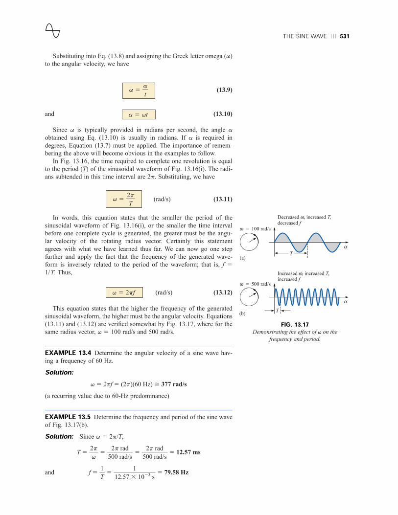
(13.11) and (13.12) are verified somewhat by Fig. 13.17, where for the
same radius vector, q 5 100 rad/s and 500 rad/s.
EXAMPLE 13.4 Determine the angular velocity of a sine wave hav-
ing a frequency of 60 Hz.
Solution:q 5 2pf 5 (2p)(60 Hz) > 377 rad/s
(a recurring value due to 60-Hz predominance)
EXAMPLE 13.5 Determine the frequency and period of the sine wave
of Fig. 13.17(b).
Solution: Since q 5 2p/T,
T 5 5 5 5 12.57 ms
and f 5 5 5 79.58 Hz1
12.57 3 1023 s
1T
2p rad500 rad/s
2p rad500 rad/s
2pq
q 5 2pf
q 5 2
T
p
a 5 qt
q 5 a
t
(a)
(b)
T
α
T
Decreased ω, increased T,decreased f
ω
Increased ω, increased T,increased f
ω
α
ω = 500 rad/sω
ω = 100 rad/sω
FIG. 13.17Demonstrating the effect of q on the
frequency and period.

0
π, 180°π 2π, 360°πα (° or rad)α
Am
Am
532 SINUSOIDAL ALTERNATING WAVEFORMS
EXAMPLE 13.6 Given q 5 200 rad/s, determine how long it will take
the sinusoidal waveform to pass through an angle of 90°.
Solution: Eq. (13.10): a 5 qt, and
t 5
However, a must be substituted as p/2 (5 90°) since q is in radians per
second:
t 5 5 5 s 5 7.85 ms
EXAMPLE 13.7 Find the angle through which a sinusoidal waveform
of 60 Hz will pass in a period of 5 ms.
Solution: Eq. (13.11): a 5 qt, or
a 5 2pft 5 (2p)(60 Hz)(5 3 1023s) 5 1.885 rad
If not careful, one might be tempted to interpret the answer as
1.885°. However,
a (°) 5 (1.885 rad) 5 108°
13.4 GENERAL FORMAT FOR THE SINUSOIDALVOLTAGE OR CURRENTThe basic mathematical format for the sinusoidal waveform is
(13.13)
where Am is the peak value of the waveform and a is the unit of mea-
sure for the horizontal axis, as shown in Fig. 13.18.
Am sin a
180°p rad
p400
p/2 rad200 rad/s
aq
aq
FIG. 13.18Basic sinusoidal function.
The equation a 5 qt states that the angle a through which the rotat-
ing vector of Fig. 13.16 will pass is determined by the angular velocity
of the rotating vector and the length of time the vector rotates. For
example, for a particular angular velocity (fixed q), the longer the
radius vector is permitted to rotate (that is, the greater the value of t),
the greater will be the number of degrees or radians through which the
vector will pass. Relating this statement to the sinusoidal waveform, for
a particular angular velocity, the longer the time, the greater the num-

GENERAL FORMAT FOR THE SINUSOIDAL VOLTAGE OR CURRENT 533
ber of cycles shown. For a fixed time interval, the greater the angular
velocity, the greater the number of cycles generated.
Due to Eq. (13.10), the general format of a sine wave can also be
written
(13.14)
with qt as the horizontal unit of measure.
For electrical quantities such as current and voltage, the general for-
mat is
i 5 Im sin qt 5 Im sin a
e 5 Em sin qt 5 Em sin a
where the capital letters with the subscript m represent the amplitude,
and the lowercase letters i and e represent the instantaneous value of
current or voltage, respectively, at any time t. This format is particularly
important since it presents the sinusoidal voltage or current as a func-
tion of time, which is the horizontal scale for the oscilloscope. Recall
that the horizontal sensitivity of a scope is in time per division and not
degrees per centimeter.
EXAMPLE 13.8 Given e 5 5 sin a, determine e at a 5 40° and a 5
0.8p .
Solution: For a 5 40°,
e 5 5 sin 40° 5 5(0.6428) 5 3.214 V
For a 5 0.8p,
a (°) 5 (0.8p) 5 144°
and e 5 5 sin 144° 5 5(0.5878) 5 2.939 V
The conversion to degrees will not be required for most modern-day
scientific calculators since they can perform the function directly. First, be
sure that the calculator is in the RAD mode. Then simply enter the radian
measure and use the appropriate trigonometric key (sin, cos, tan, etc.).
The angle at which a particular voltage level is attained can be
determined by rearranging the equation
e 5 Em sin a
in the following manner:
sin a 5
which can be written
(13.15)
Similarly, for a particular current level,
(13.16)
The function sin21 is available on all scientific calculators.
a 5 sin21I
i
m
a 5 sin21E
e
m
eEm
180°
p
Am sin qt

0 α (rad)απ2—π
6—
π32
—π π2
10
e
10
10
0° 30° 90°
180° 270° 360°
α (°)α
e
10
534 SINUSOIDAL ALTERNATING WAVEFORMS
EXAMPLE 13.9a. Determine the angle at which the magnitude of the sinusoidal func-
tion v 5 10 sin 377t is 4 V.
b. Determine the time at which the magnitude is attained.
Solutions:a. Eq. (13.15):
a1 5 sin215 sin21
5 sin21 0.4 5 23.578°
However, Figure 13.19 reveals that the magnitude of 4 V (posi-
tive) will be attained at two points between 0° and 180°. The second
intersection is determined by
a2 5 180° 2 23.578° 5 156.422°
In general, therefore, keep in mind that Equations (13.15) and
(13.16) will provide an angle with a magnitude between 0° and 90°.
b. Eq. (13.10): a 5 qt, and so t 5 a /q. However, a must be in radians.
Thus,
a (rad) 5 (23.578°) 5 0.411 rad
and t1 5 5 5 1.09 ms
For the second intersection,
a (rad) 5 (156.422°) 5 2.73 rad
t2 5 5 5 7.24 ms
The sine wave can also be plotted against time on the horizontal
axis. The time period for each interval can be determined from t 5 a /q,
but the most direct route is simply to find the period T from T 5 1/f and
break it up into the required intervals. This latter technique will be
demonstrated in Example 13.10.
Before reviewing the example, take special note of the relative sim-
plicity of the mathematical equation that can represent a sinusoidal
waveform. Any alternating waveform whose characteristics differ from
those of the sine wave cannot be represented by a single term, but may
require two, four, six, or perhaps an infinite number of terms to be rep-
resented accurately. Additional description of nonsinusoidal waveforms
can be found in Chapter 25.
EXAMPLE 13.10 Sketch e 5 10 sin 314t with the abscissa
a. angle (a) in degrees.
b. angle (a) in radians.
c. time (t) in seconds.
Solutions:a. See Fig 13.20. (Note that no calculations are required.)
b. See Fig. 13.21. (Once the relationship between degrees and radians
is understood, there is again no need for calculations.)
2.73 rad377 rad/s
aq
p180°
0.411 rad377 rad/s
aq
p180°
4 V10 V
vEm
v (V)
4
1 90°
10
0
t1
2
t2
180° aaa
FIG. 13.19Example 13.9.
FIG. 13.20Example 13.10, horizontal axis in degrees.
FIG. 13.21Example 13.10, horizontal axis in radians.

0 1.67
10 15 20
10
T = 20 ms
t (ms)5
10
PHASE RELATIONS 535
c. 360°: T 5 5 5 20 ms
180°: 5 5 10 ms
90°: 5 5 5 ms
30°: 5 5 1.67 ms
See Fig. 13.22.
EXAMPLE 13.11 Given i 5 6 3 1023 sin 1000t, determine i at t 5
2 ms.
Solution:a 5 qt 5 1000t 5 (1000 rad/s)(2 3 1023 s) 5 2 rad
a (°) 5 (2 rad) 5 114.59°
i 5 (6 3 1023)(sin 114.59°)
5 (6 mA)(0.9093) 5 5.46 mA
13.5 PHASE RELATIONSThus far, we have considered only sine waves that have maxima at p/2
and 3p/2, with a zero value at 0, p, and 2p, as shown in Fig. 13.21. If the
waveform is shifted to the right or left of 0°, the expression becomes
(13.17)
where v is the angle in degrees or radians that the waveform has been
shifted.
If the waveform passes through the horizontal axis with a positive-
going (increasing with time) slope before 0°, as shown in Fig. 13.23,
the expression is
(13.18)
At qt 5 a 5 0°, the magnitude is determined by Am sin v. If the wave-
form passes through the horizontal axis with a positive-going slope
after 0°, as shown in Fig. 13.24, the expression is
(13.19)
And at qt 5 a 5 0°, the magnitude is Am sin(2v), which, by a trigono-
metric identity, is 2Am sin v.
If the waveform crosses the horizontal axis with a positive-going slope
90° (p/2) sooner, as shown in Fig. 13.25, it is called a cosine wave; that is,
sin(qt 1 90°) 5 sin1qt 1 p
22 5 cos qt (13.20)
Am sin(qt 2 v)
Am sin(qt 1 v)
Am sin(qt 6 v)
180°p rad
20 ms
12
T12
20 ms
4
T4
20 ms
2
T2
2p314
2pq
FIG. 13.22Example 13.10, horizontal axis in
milliseconds.
u
( – )
Am
(2 – )
a
Am sinup u
p u
FIG. 13.23Defining the phase shift for a sinusoidal
function that crosses the horizontal axis with
a positive slope before 0°.
v (p + v)
Am
(2p + v)
a– Am sin v
FIG. 13.24Defining the phase shift for a sinusoidal
function that crosses the horizontal axis with
a positive slope after 0°.
0
Am
90°
cos asin a
p 2p
a
p2
– p2
p32
FIG. 13.25Phase relationship between a sine wave and a
cosine wave.

536 SINUSOIDAL ALTERNATING WAVEFORMS
or sin qt 5 cos(qt 2 90°) 5 cos1qt 2 p
22 (13.21)
The terms lead and lag are used to indicate the relationship
between two sinusoidal waveforms of the same frequency plotted on
the same set of axes. In Fig. 13.25, the cosine curve is said to lead
the sine curve by 90°, and the sine curve is said to lag the cosine
curve by 90°. The 90° is referred to as the phase angle between the
two waveforms. In language commonly applied, the waveforms are
out of phase by 90°. Note that the phase angle between the two
waveforms is measured between those two points on the horizontal
axis through which each passes with the same slope. If both wave-
forms cross the axis at the same point with the same slope, they are
in phase.
The geometric relationship between various forms of the sine and
cosine functions can be derived from Fig. 13.26. For instance, starting
at the sin a position, we find that cos a is an additional 90° in the coun-
terclockwise direction. Therefore, cos a 5 sin(a 1 90°). For 2sin a
we must travel 180° in the counterclockwise (or clockwise) direction so
that 2sin a 5 sin(a 6 180°), and so on, as listed below:
(13.22)
In addition, one should be aware that
(13.23)
If a sinusoidal expression should appear as
e 5 2Em sin qt
the negative sign is associated with the sine portion of the expression,
not the peak value Em. In other words, the expression, if not for conve-
nience, would be written
e 5 Em(2sin qt)
Since
2sin qt 5 sin(qt 6 180°)
the expression can also be written
e 5 Em sin(qt 6 180°)
revealing that a negative sign can be replaced by a 180° change in
phase angle (1 or 2); that is,
e 5 Em sin qt 5 Em sin(qt 1 180°)
5 Em sin(qt 2 180°)
A plot of each will clearly show their equivalence. There are, there-
fore, two correct mathematical representations for the functions.
sin(2a) 5 2sin a
cos(2a) 5 cos a
cos a 5 sin(a 1 90°)
sin a 5 cos(a 2 90°)
2sin a 5 sin(a 6 180°)
2cos a 5 sin(a 1 270°) 5 sin(a 2 90°)
etc.
+cos
–cos
+sin–sin
α
α α
α
FIG. 13.26Graphic tool for finding the relationship
between specific sine and cosine functions.

PHASE RELATIONS 537
The phase relationship between two waveforms indicates which
one leads or lags, and by how many degrees or radians.
EXAMPLE 13.12 What is the phase relationship between the sinu-
soidal waveforms of each of the following sets?
a. v 5 10 sin(qt 1 30°)
i 5 5 sin(qt 1 70°)
b. i 5 15 sin(qt 1 60°)
v 5 10 sin(qt 2 20°)
c. i 5 2 cos(qt 1 10°)
v 5 3 sin(qt 2 10°)
d. i 5 2sin(qt 1 30°)
v 5 2 sin(qt 1 10°)
e. i 5 22 cos(qt 2 60°)
v 5 3 sin(qt 2 150°)
Solutions:a. See Fig. 13.27.
i leads v by 40°, or v lags i by 40°.
v
30°40°
5
10
i
02
p32
2 vt
70°
p
p
p
FIG. 13.27Example 13.12; i leads v by 40°.
b. See Fig. 13.28.
i leads v by 80°, or v lags i by 80°.
10 15
i
v
2–
2
p 3
2p
2 vt
20°80°
60°
0p p p
FIG. 13.28Example 13.12; i leads v by 80°.

538 SINUSOIDAL ALTERNATING WAVEFORMS
d. See Fig. 13.30.Note
2sin(qt 1 30°) 5 sin(qt 1 30° 2 180°)
5 sin(qt 2 150°)
v leads i by 160°, or i lags v by 160°.
i
v23
10°
110°
2
0 p 3
2p
2 vt
100°
p
2––
p p p
FIG. 13.29Example 13.12; i leads v by 110°.
2
1
2– 3
2p
p2
2
5
2p
3vt
10°160°
200°360°
0
i
v
150°
p
p
p
p
FIG. 13.30Example 13.12; v leads i by 160°.
Or usingNote
2sin(qt 1 30°) 5 sin(qt 1 30° 1 180°)
5 sin(qt 1 210°)
i leads v by 200°, or v lags i by 200°.
e. See Fig. 13.31.By choice
i 5 22 cos(qt 2 60°) 5 2 cos(qt 2 60° 2 180°)
5 2 cos(qt 2 240°)
2–
3
2p
p
2
2 52p 3
vt0
i
v
150°
23
p p p p
FIG. 13.31Example 13.12; v and i are in phase.
c. See Fig. 13.29.
i 5 2 cos(qt 1 10°) 5 2 sin(qt 1 10° 1 90°)
5 2 sin(qt 1 100°)
i leads v by 110°, or v lags i by 110°.

AVERAGE VALUE 539
However, cos a 5 sin(a 1 90°)
so that 2 cos(qt 2 240°) 5 2 sin(qt 2 240° 1 90°)
5 2 sin(qt 2 150°)
v and i are in phase.
Phase MeasurementsThe hookup procedure for using an oscilloscope to measure phase
angles is covered in detail in Section 15.13. However, the equation for
determining the phase angle can be introduced using Fig. 13.32. First,
note that each sinusoidal function has the same frequency, permitting
the use of either waveform to determine the period. For the waveform
chosen in Fig. 13.32, the period encompasses 5 divisions at 0.2 ms/div.
The phase shift between the waveforms (irrespective of which is lead-
ing or lagging) is 2 divisions. Since the full period represents a cycle of
360°, the following ratio [from which Equation (13.24) can be derived]
can be formed:
5
and v 5 3 360° (13.24)
Substituting into Eq. (13.24) will result in
v 5 3 360° 5 144°
and e leads i by 144°.
13.6 AVERAGE VALUEEven though the concept of the average value is an important one in
most technical fields, its true meaning is often misunderstood. In Fig.
13.33(a), for example, the average height of the sand may be required
to determine the volume of sand available. The average height of the
sand is that height obtained if the distance from one end to the other
is maintained while the sand is leveled off, as shown in Fig. 13.33(b).
The area under the mound of Fig. 13.33(a) will then equal the area
under the rectangular shape of Fig. 13.33(b) as determined by A 5
b 3 h. Of course, the depth (into the page) of the sand must be the
same for Fig. 13.33(a) and (b) for the preceding conclusions to have
any meaning.
In Fig. 13.33 the distance was measured from one end to the other.
In Fig. 13.34(a) the distance extends beyond the end of the original pile
of Fig. 13.33. The situation could be one where a landscaper would like
to know the average height of the sand if spread out over a distance
such as defined in Fig. 13.34(a). The result of an increased distance is
as shown in Fig. 13.34(b). The average height has decreased compared
to Fig. 13.33. Quite obviously, therefore, the longer the distance, the
lower is the average value.
(2 div.)(5 div.)
phase shift (no. of div.)
T (no. of div.)
vphase shift (no. of div.)
360°T (no. of div.) Vertical sensitivity = 2 V/div.
Horizontal sensitivity = 0.2 ms/div.
T
θ
ei
FIG. 13.32Finding the phase angle between waveforms
using a dual-trace oscilloscope.
Height
Distance
Sand
(a)
Height
Average height
Sand
Samedistance
(b)
FIG. 13.33Defining average value.

540 SINUSOIDAL ALTERNATING WAVEFORMS
If the distance parameter includes a depression, as shown in Fig.
13.35(a), some of the sand will be used to fill the depression, resulting
in an even lower average value for the landscaper, as shown in Fig.
13.35(b). For a sinusoidal waveform, the depression would have the
same shape as the mound of sand (over one full cycle), resulting in an
average value at ground level (or zero volts for a sinusoidal voltage over
one full period).
After traveling a considerable distance by car, some drivers like to
calculate their average speed for the entire trip. This is usually done by
dividing the miles traveled by the hours required to drive that distance.
For example, if a person traveled 225 mi in 5 h, the average speed was
225 mi/5 h, or 45 mi/h. This same distance may have been traveled at
various speeds for various intervals of time, as shown in Fig. 13.36.
By finding the total area under the curve for the 5 h and then divid-
ing the area by 5 h (the total time for the trip), we obtain the same result
of 45 mi/h; that is,
Average speed 5 (13.25)
Average speed 5
5
5 mi/h
5 45 mi/h
Equation (13.25) can be extended to include any variable quantity, such
as current or voltage, if we let G denote the average value, as follows:
G (average value) 5 (13.26)algebraic sum of areas
length of curve
225
5
(60 mi/h)(2 h) 1 (50 mi/h)(2.5 h)
5 h
A1 1 A2
5 h
area under curvelength of curve
Height
Distance
Sand
(a)
Height
Average height
Sand
Samedistance
(b)
FIG. 13.34Effect of distance (length) on average value.
Height
Distance
(a)
Height
Average height
Sand
Samedistance
(b)
Sand
Ground level
FIG. 13.35Effect of depressions (negative excursions) on
average value.
10203040506070
Speed (mi/h)
A1 A2
0 1 2 3 4 5 6 t (h)Lunch break
Average speed
FIG. 13.36Plotting speed versus time for an automobile excursion.
The algebraic sum of the areas must be determined, since some area
contributions will be from below the horizontal axis. Areas above the
axis will be assigned a positive sign, and those below, a negative sign.
A positive average value will then be above the axis, and a negative
value, below.
The average value of any current or voltage is the value indicated on
a dc meter. In other words, over a complete cycle, the average value is

AVERAGE VALUE 541
the equivalent dc value. In the analysis of electronic circuits to be con-
sidered in a later course, both dc and ac sources of voltage will be
applied to the same network. It will then be necessary to know or deter-
mine the dc (or average value) and ac components of the voltage or cur-
rent in various parts of the system.
EXAMPLE 13.13 Determine the average value of the waveforms of
Fig. 13.37.
0
10 V
1 2 3 4 t (ms)
–10 V
(a)
0
14 V
1 2 3 4 t (ms)
–6 V
(b)
v1
v2
(Square wave)
FIG. 13.37Example 13.13.
Solutions:a. By inspection, the area above the axis equals the area below over
one cycle, resulting in an average value of zero volts. Using Eq.
(13.26):
G 5
5 5 0 V
b. Using Eq. (13.26):
G 5
5 5 5 4 V
as shown in Fig. 13.38.
In reality, the waveform of Fig. 13.37(b) is simply the square wave
of Fig. 13.37(a) with a dc shift of 4 V; that is,
v2 5 v1 1 4 V
EXAMPLE 13.14 Find the average values of the following waveforms
over one full cycle:
a. Fig. 13.39.
b. Fig. 13.40.
8 V
2
14 V 2 6 V
2
(14 V)(1 ms) 2 (6 V)(1 ms)
2 ms
02 ms
(10 V)(1 ms) 2 (10 V)(1 ms)
2 ms
14 V
4 V
0–6 V
1 2 3 4 t (ms)
FIG. 13.38Defining the average value for the waveform
of Fig. 13.37(b).
3
v (V)
0
–1
4 8
t (ms)
1 cycle
FIG. 13.39Example 13.14, part (a).

0 π2— π
Am
0 π2— π
Am
π3— π2
3—
542 SINUSOIDAL ALTERNATING WAVEFORMS
Solutions:a. G 5 5 5 1 V
Note Fig. 13.41.
b. G 5
5 5 2 5 21.6 V
Note Fig. 13.42.
We found the areas under the curves in the preceding example by
using a simple geometric formula. If we should encounter a sine wave
or any other unusual shape, however, we must find the area by some
other means. We can obtain a good approximation of the area by
attempting to reproduce the original wave shape using a number of
small rectangles or other familiar shapes, the area of which we already
know through simple geometric formulas. For example,
the area of the positive (or negative) pulse of a sine wave is 2Am.
Approximating this waveform by two triangles (Fig. 13.43), we obtain
(using area 5 1/2 base 3 height for the area of a triangle) a rough idea
of the actual area:
b h
Area shaded 5 21 bh2 5 231 21 2(Am)4 5 Am
> 1.58Am
A closer approximation might be a rectangle with two similar trian-
gles (Fig. 13.44):
Area 5 Am 1 21 bh2 5 Am 1 Am5 pAm
5 2.094Am
which is certainly close to the actual area. If an infinite number of
forms were used, an exact answer of 2Am could be obtained. For irreg-
ular waveforms, this method can be especially useful if data such as the
average value are desired.
The procedure of calculus that gives the exact solution 2Am is
known as integration. Integration is presented here only to make the
23
p3
p3
12
p3
p2
p2
12
12
16 V
10
220 V 1 8 V 2 4 V
10
2(10 V)(2 ms) 1 (4 V)(2 ms) 2 (2 V)(2 ms)
10 ms
12 V 2 4 V
8
1(3 V)(4 ms) 2 (1 V)(4 ms)
8 ms
1 cycle
2 46 8
10 t (ms)
i (A)
4
0
–2
–10
FIG. 13.40Example 13.14, part (b).
1
vav (V)
8 t (ms)
1V0
dc voltmeter (between 0 and 8 ms)
FIG. 13.41The response of a dc meter to the waveform of
Fig. 13.39.
0
–1.6
iav (A)
t (ms)
dc ammeter (between 0 and 10 ms)
– +–1.6
10
FIG. 13.42The response of a dc meter to the waveform of
Fig. 13.40.
FIG. 13.43Approximating the shape of the positive pulse
of a sinusoidal waveform with two right
triangles.
FIG. 13.44A better approximation for the shape of the
positive pulse of a sinusoidal waveform.

0 π α
Am
π2
—
AVERAGE VALUE 543
method recognizable to the reader; it is not necessary to be proficient in
its use to continue with this text. It is a useful mathematical tool, how-
ever, and should be learned. Finding the area under the positive pulse of
a sine wave using integration, we have
Area 5 Ep
0
Am sin a da
where ∫ is the sign of integration, 0 and p are the limits of integration,
Am sin a is the function to be integrated, and da indicates that we are
integrating with respect to a.
Integrating, we obtain
Area 5 Am[2cos a]p05 2Am(cos p 2 cos 0°)
5 2Am[21 2 (11)] 5 2Am(22)
(13.27)
Since we know the area under the positive (or negative) pulse, we
can easily determine the average value of the positive (or negative)
region of a sine wave pulse by applying Eq. (13.26):
G 5
and (13.28)
For the waveform of Fig. 13.45,
G 5 5(average the same
as for a full pulse)
EXAMPLE 13.15 Determine the average value of the sinusoidal
waveform of Fig. 13.46.
Solution: By inspection it is fairly obvious that
the average value of a pure sinusoidal waveform over one full cycle is
zero.
Eq. (13.26):
G 5 5 0 V
EXAMPLE 13.16 Determine the average value of the waveform of
Fig. 13.47.
Solution: The peak-to-peak value of the sinusoidal function is
16 mV 1 2 mV 5 18 mV. The peak amplitude of the sinusoidal wave-
form is, therefore, 18 mV/2 5 9 mV. Counting down 9 mV from 2 mV
(or 9 mV up from 216 mV) results in an average or dc level of 27 mV,
as noted by the dashed line of Fig. 13.47.
12Am 2 2Am
2p
2Amp
(2Am/2)
p/2
G Am
0 p
G 5 0.637Am
2Amp
Am
0 p
Area 5 2Am
FIG. 13.45Finding the average value of one-half the
positive pulse of a sinusoidal waveform.
0
1 cycle
Am
Am
π 2 απ
FIG. 13.46Example 13.15.
+2 mV
v
0t
–16 mV
FIG. 13.47Example 13.16.

544 SINUSOIDAL ALTERNATING WAVEFORMS
EXAMPLE 13.17 Determine the average value of the waveform of
Fig. 13.48.
Solution:G 5 5 > 3.18 V
EXAMPLE 13.18 For the waveform of Fig. 13.49, determine whether
the average value is positive or negative, and determine its approximate
value.
Solution: From the appearance of the waveform, the average value
is positive and in the vicinity of 2 mV. Occasionally, judgments of this
type will have to be made.
InstrumentationThe dc level or average value of any waveform can be found using a
digital multimeter (DMM) or an oscilloscope. For purely dc circuits,
simply set the DMM on dc, and read the voltage or current levels.
Oscilloscopes are limited to voltage levels using the sequence of steps
listed below:
1. First choose GND from the DC-GND-AC option list associated
with each vertical channel. The GND option blocks any signal to
which the oscilloscope probe may be connected from entering the
oscilloscope and responds with just a horizontal line. Set the
resulting line in the middle of the vertical axis on the horizontal
axis, as shown in Fig. 13.50(a).
2(10 V)
2p
2Am 1 0
2p
v (mV)
10 mV
0t
FIG. 13.49Example 13.18.
(b)
Vertical sensitivity = 50 mV/div.
Shift = 2.5 div.
(a)
FIG. 13.50Using the oscilloscope to measure dc voltages: (a) setting the GND condition;
(b) the vertical shift resulting from a dc voltage when shifted to the DC option.
2. Apply the oscilloscope probe to the voltage to be measured (if
not already connected), and switch to the DC option. If a dc volt-
age is present, the horizontal line will shift up or down, as
demonstrated in Fig. 13.50(b). Multiplying the shift by the verti-
cal sensitivity will result in the dc voltage. An upward shift is a
positive voltage (higher potential at the red or positive lead of the
oscilloscope), while a downward shift is a negative voltage
(lower potential at the red or positive lead of the oscilloscope).
a1
1 cycle
2pp
v (V)
10
0
Sine wave
FIG. 13.48Example 13.17.

AVERAGE VALUE 545
In general,
Shift = 0.9 div.
(a)
Reference
level
(b)
FIG. 13.51Determining the average value of a nonsinusoidal waveform using the
oscilloscope: (a) vertical channel on the ac mode; (b) vertical channel on the
dc mode.
The procedure outlined above can be applied to any alternating
waveform such as the one in Fig. 13.49. In some cases the average
value may require moving the starting position of the waveform under
the AC option to a different region of the screen or choosing a higher
voltage scale. DMMs can read the average or dc level of any waveform
by simply choosing the appropriate scale.
(13.29)Vdc 5 (vertical shift in div.) 3 (vertical sensitivity in V/div.)
For the waveform of Fig. 13.50(b),
Vdc 5 (2.5 div.)(50 mV/div.) 5 125 mV
The oscilloscope can also be used to measure the dc or average level
of any waveform using the following sequence:
1. Using the GND option, reset the horizontal line to the middle of
the screen.
2. Switch to AC (all dc components of the signal to which the probe
is connected will be blocked from entering the oscilloscope—
only the alternating, or changing, components will be displayed).
Note the location of some definitive point on the waveform, such
as the bottom of the half-wave rectified waveform of Fig.
13.51(a); that is, note its position on the vertical scale. For the
future, whenever you use the AC option, keep in mind that the
computer will distribute the waveform above and below the hori-
zontal axis such that the average value is zero; that is, the area
above the axis will equal the area below.
3. Then switch to DC (to permit both the dc and the ac components
of the waveform to enter the oscilloscope), and note the shift in
the chosen level of part 2, as shown in Fig. 13.51(b). Equation
(13.29) can then be used to determine the dc or average value of
the waveform. For the waveform of Fig. 13.51(b), the average
value is about
Vav 5 Vdc 5 (0.9 div.)(5 V/div.) 5 4.5 V

546 SINUSOIDAL ALTERNATING WAVEFORMS
13.7 EFFECTIVE (rms) VALUESThis section will begin to relate dc and ac quantities with respect to
the power delivered to a load. It will help us determine the amplitude
of a sinusoidal ac current required to deliver the same power as a
particular dc current. The question frequently arises, How is it possi-
ble for a sinusoidal ac quantity to deliver a net power if, over a full
cycle, the net current in any one direction is zero (average value 5
0)? It would almost appear that the power delivered during the posi-
tive portion of the sinusoidal waveform is withdrawn during the neg-
ative portion, and since the two are equal in magnitude, the net
power delivered is zero. However, understand that irrespective of
direction, current of any magnitude through a resistor will deliver
power to that resistor. In other words, during the positive or negative
portions of a sinusoidal ac current, power is being delivered at each
instant of time to the resistor. The power delivered at each instant
will, of course, vary with the magnitude of the sinusoidal ac current,
but there will be a net flow during either the positive or the negative
pulses with a net flow over the full cycle. The net power flow will
equal twice that delivered by either the positive or the negative
regions of sinusoidal quantity.
A fixed relationship between ac and dc voltages and currents can be
derived from the experimental setup shown in Fig. 13.52. A resistor in
a water bath is connected by switches to a dc and an ac supply. If switch
1 is closed, a dc current I, determined by the resistance R and battery
voltage E, will be established through the resistor R. The temperature
reached by the water is determined by the dc power dissipated in the
form of heat by the resistor.
Switch 2
iac
ac generatore
Switch 1
dc sourceE
R
Idc
FIG. 13.52An experimental setup to establish a relationship between dc and ac quantities.
If switch 2 is closed and switch 1 left open, the ac current through
the resistor will have a peak value of Im. The temperature reached by
the water is now determined by the ac power dissipated in the form of
heat by the resistor. The ac input is varied until the temperature is the
same as that reached with the dc input. When this is accomplished, the
average electrical power delivered to the resistor R by the ac source is
the same as that delivered by the dc source.
The power delivered by the ac supply at any instant of time is
Pac 5 (iac)2R 5 (Im sin qt)2R 5 (I 2m sin2qt)R
but
sin2qt 5 (1 2 cos 2qt) (trigonometric identity)12

EFFECTIVE (rms) VALUES 547
Therefore,
Pac 5 I 2m3 (1 2 cos 2qt)4R
and (13.30)
The average power delivered by the ac source is just the first term,
since the average value of a cosine wave is zero even though the wave
may have twice the frequency of the original input current waveform.
Equating the average power delivered by the ac generator to that deliv-
ered by the dc source,
Pav(ac) 5 Pdc
5 I 2dcR and Im 5 Ï2wIdc
or Idc 5 5 0.707Im
which, in words, states that
the equivalent dc value of a sinusoidal current or voltage is 1/ Ï2w or
0.707 of its maximum value.
The equivalent dc value is called the effective value of the sinusoidal
quantity.
In summary,
(13.31)
or (13.32)
and (13.33)
or (13.34)
As a simple numerical example, it would require an ac current with
a peak value of Ï2w(10) 5 14.14 A to deliver the same power to the
resistor in Fig. 13.52 as a dc current of 10 A. The effective value of any
quantity plotted as a function of time can be found by using the fol-
lowing equation derived from the experiment just described:
Ieff 5 !§ (13.35)
or Ieff 5 !§ (13.36)area (i2(t))
T
ET
0
i2(t) dt
T
Em 5 Ï2wEeff 5 1.414Eeff
Eeff 5 0.707Em
Im 5 Ï2wIeff 5 1.414Ieff
Ieq(dc) 5 Ieff 5 0.707Im
ImÏ2w
I2mR2
Pac 5 I 2m
2
R 2
I 2m
2
R cos 2qt
12

548 SINUSOIDAL ALTERNATING WAVEFORMS
which, in words, states that to find the effective value, the function i(t)
must first be squared. After i(t) is squared, the area under the curve is
found by integration. It is then divided by T, the length of the cycle or
the period of the waveform, to obtain the average or mean value of the
squared waveform. The final step is to take the square root of the mean
value. This procedure gives us another designation for the effective
value, the root-mean-square (rms) value. In fact, since the rms term is
the most commonly used in the educational and industrial communities,
it will used throughout this text.
EXAMPLE 13.19 Find the rms values of the sinusoidal waveform in
each part of Fig. 13.53.
12
i (mA)
0 1st
12
i (mA)
0t
1s 2 st
v
169.7 V
(c)(b)(a)
FIG. 13.53Example 13.19.
Solution: For part (a), Irms 5 0.707(12 3 1023 A) 5 8.484 mA.
For part (b), again Irms 5 8.484 mA. Note that frequency did not
change the effective value in (b) above compared to (a). For part (c),
Vrms 5 0.707(169.73 V) > 120 V, the same as available from a home
outlet.
EXAMPLE 13.20 The 120-V dc source of Fig. 13.54(a) delivers
3.6 W to the load. Determine the peak value of the applied voltage
(Em) and the current (Im) if the ac source [Fig. 13.54(b)] is to
deliver the same power to the load.
iac
–
P = 3.6 WLoad
Em
Idc
E 120 V P = 3.6 WLoad
e
Im
+
(b)(a)
FIG. 13.54Example 13.20.

EFFECTIVE (rms) VALUES 549
Solution:Pdc 5 VdcIdc
and Idc 5 5 5 30 mA
Im 5 Ï2wIdc 5 (1.414)(30 mA) 5 42.42 mA
Em 5 Ï2wEdc 5 (1.414)(120 V) 5 169.68 V
EXAMPLE 13.21 Find the effective or rms value of the waveform of
Fig. 13.55.
Solution:v2 (Fig. 13.56):
Vrms 5 !§ 5 !§ 5 2.236 V
EXAMPLE 13.22 Calculate the rms value of the voltage of Fig. 13.57.
408
(9)(4) 1 (1)(4)
8
3.6 W120 V
PdcVdc
1 cycle
t (s)
840
3
–1
v (V)
9
v2 (V)
1
0 4 8 t (s)
(– 1)2 = 1
1 cycle
4
v (V)
0–2
–10
4 6 8 10 t (s)
FIG. 13.55Example 13.21.
FIG. 13.56The squared waveform of Fig. 13.55.
FIG. 13.57Example 13.22.
Solution:v2 (Fig. 13.58):
Vrms 5 !§§ 5 !§5 4.899 V
24010
(100)(2) 1 (16)(2) 1 (4)(2)
10
100
2 4 6 8 10
164
0 t (s)
v2 (V)
FIG. 13.58The squared waveform of Fig. 13.57.

550 SINUSOIDAL ALTERNATING WAVEFORMS
EXAMPLE 13.23 Determine the average and rms values of the square
wave of Fig. 13.59.
Solution: By inspection, the average value is zero.
v2 (Fig. 13.60):
Vrms 5 !§§§5 !§5 Ï1w6w0w0w
Vrms 5 40 V
(the maximum value of the waveform of Fig. 13.60)
The waveforms appearing in these examples are the same as those
used in the examples on the average value. It might prove interesting to
compare the rms and average values of these waveforms.
The rms values of sinusoidal quantities such as voltage or current
will be represented by E and I. These symbols are the same as those
used for dc voltages and currents. To avoid confusion, the peak value
of a waveform will always have a subscript m associated with it: Im
sin qt. Caution: When finding the rms value of the positive pulse of a
sine wave, note that the squared area is not simply (2Am)25 4A2
m; it
must be found by a completely new integration. This will always be
the case for any waveform that is not rectangular.
A unique situation arises if a waveform has both a dc and an ac com-
ponent that may be due to a source such as the one in Fig. 13.61. The
combination appears frequently in the analysis of electronic networks
where both dc and ac levels are present in the same system.
32,000 3 1023
20 3 1023
(1600)(10 3 1023) 1 (1600)(10 3 1023)
20 3 1023
20100
v2 (V)
1600
t (ms)
FIG. 13.60The squared waveform of Fig. 13.59.
3 sin t+
–
6 V
vT
+
–
vT
7.5 V
6 V
4.5 V
0 t
ω
FIG. 13.61Generation and display of a waveform having a dc and an ac component.
The question arises, What is the rms value of the voltage vT? One
might be tempted to simply assume that it is the sum of the rms values
of each component of the waveform; that is, VT rms5 0.7071(1.5 V) 1
6 V 5 1.06 V 1 6 V 5 7.06 V. However, the rms value is actually
determined by
Vrms 5 ÏVw2dcw 1w Vw2
acw(rmws)w (13.37)
which for the above example is
Vrms 5 Ï(6w Vw)2w 1w (w1w.0w6w Vw)2w5 Ï3w7w.1w2w4w V
> 6.1 V
40
0
–40
10 20 t (ms)
v (V)
1 cycle
FIG. 13.59Example 13.23.

ac METERS AND INSTRUMENTS 551
This result is noticeably less than the above solution. The development
of Eq. (13.37) can be found in Chapter 25.
InstrumentationIt is important to note whether the DMM in use is a true rms meter or
simply a meter where the average value is calibrated (as described in
the next section) to indicate the rms level. A true rms meter will read
the effective value of any waveform (such as Figs. 13.49 and 13.61)
and is not limited to only sinusoidal waveforms. Since the label true
rms is normally not placed on the face of the meter, it is prudent to
check the manual if waveforms other than purely sinusoidal are to be
encountered. For any type of rms meter, be sure to check the manual for
its frequency range of application. For most it is less than 1 kHz.
13.8 ac METERS AND INSTRUMENTSThe d’Arsonval movement employed in dc meters can also be used to
measure sinusoidal voltages and currents if the bridge rectifier of Fig.
13.62 is placed between the signal to be measured and the average read-
ing movement.
The bridge rectifier, composed of four diodes (electronic switches),
will convert the input signal of zero average value to one having an
average value sensitive to the peak value of the input signal. The con-
version process is well described in most basic electronics texts. Fun-
damentally, conduction is permitted through the diodes in such a man-
ner as to convert the sinusoidal input of Fig. 13.63(a) to one having the
appearance of Fig. 13.63(b). The negative portion of the input has been
effectively “flipped over” by the bridge configuration. The resulting
waveform of Fig. 13.63(b) is called a full-wave rectified waveform.
vmovement
vi
+
–
+–
FIG. 13.62Full-wave bridge rectifier.
vi
Vm
–Vm
0 p 2 a
(a)
vmovement
Vm
0 p 2 a
(b)
Vdc = 0.637Vm
p p
FIG. 13.63(a) Sinusoidal input; (b) full-wave rectified signal.
The zero average value of Fig. 13.63(a) has been replaced by a pat-
tern having an average value determined by
G 5 5 5 5 0.637Vm
The movement of the pointer will therefore be directly related to the
peak value of the signal by the factor 0.637.
Forming the ratio between the rms and dc levels will result in
5 > 1.110.707Vm0.637Vm
VrmsVdc
2Vmp
4Vm2p
2Vm 1 2Vm
2p

552 SINUSOIDAL ALTERNATING WAVEFORMS
revealing that the scale indication is 1.11 times the dc level measured
by the movement; that is,
full-wave (13.38)
Some ac meters use a half-wave rectifier arrangement that results in
the waveform of Fig. 13.64, which has half the average value of Fig.
13.63(b) over one full cycle. The result is
half-wave (13.39)
A second movement, called the electrodynamometer movement
(Fig. 13.65), can measure both ac and dc quantities without a change in
internal circuitry. The movement can, in fact, read the effective value of
any periodic or nonperiodic waveform because a reversal in current
direction reverses the fields of both the stationary and the movable
coils, so the deflection of the pointer is always up-scale.
The VOM, introduced in Chapter 2, can be used to measure both dc
and ac voltages using a d’Arsonval movement and the proper switching
networks. That is, when the meter is used for dc measurements, the dial
setting will establish the proper series resistance for the chosen scale
and will permit the appropriate dc level to pass directly to the move-
ment. For ac measurements, the dial setting will introduce a network
that employs a full- or half-wave rectifier to establish a dc level. As dis-
cussed above, each setting is properly calibrated to indicate the desired
quantity on the face of the instrument.
EXAMPLE 13.24 Determine the reading of each meter for each situ-
ation of Fig. 13.66(a) and (b).
Meter indication 5 2.22 (dc or average value)
Meter indication 5 1.11 (dc or average value)
Vm
vmovement
Vdc = 0.318Vm
p 2p
FIG. 13.64Half-wave rectified signal.
FIG. 13.65Electrodynamometer movement. (Courtesy of
Weston Instruments, Inc.)
(1)
20 V
+
–
dc
(2)
Vm = 20 V
+
–
ac
(a)
d’Arsonvalmovement
rms scale
(full-waverectifier)
Voltmeter
(1)
+
–
dc
(2)
+
–
(b)
Electrodynamometermovement
rms scale
Voltmeter
25 V e = 15 sin 200t
FIG. 13.66Example 13.24.

ac METERS AND INSTRUMENTS 553
Solution: For Fig. 13.66(a), situation (1): By Eq. (13.38),
Meter indication 5 1.11(20 V) 5 22.2 V
For Fig. 13.66(a), situation (2):
Vrms 5 0.707Vm 5 0.707(20 V) 5 14.14 V
For Fig. 13.66(b), situation (1):
Vrms 5 Vdc 5 25 V
For Fig. 13.66(b), situation (2):
Vrms 5 0.707Vm 5 0.707(15 V) > 10.6 V
Most DMMs employ a full-wave rectification system to convert the
input ac signal to one with an average value. In fact, for the DMM of
Fig. 2.27, the same scale factor of Eq. (13.38) is employed; that is, the
average value is scaled up by a factor of 1.11 to obtain the rms value.
In digital meters, however, there are no moving parts such as in the
d’Arsonval or electrodynamometer movements to display the signal
level. Rather, the average value is sensed by a multiprocessor integrated
circuit (IC), which in turn determines which digits should appear on the
digital display.
Digital meters can also be used to measure nonsinusoidal signals,
but the scale factor of each input waveform must first be known (nor-
mally provided by the manufacturer in the operator’s manual). For
instance, the scale factor for an average responding DMM on the ac rms
scale will produce an indication for a square-wave input that is 1.11
times the peak value. For a triangular input, the response is 0.555 times
the peak value. Obviously, for a sine wave input, the response is 0.707
times the peak value.
For any instrument, it is always good practice to read (if only briefly)
the operator’s manual if it appears that you will use the instrument on a
regular basis.
For frequency measurements, the frequency counter of Fig. 13.67
provides a digital readout of sine, square, and triangular waves from
5 Hz to 100 MHz at input levels from 30 mV to 42 V. Note the relative
simplicity of the panel and the high degree of accuracy available.
The Amp-Clamp® of Fig. 13.68 is an instrument that can measure
alternating current in the ampere range without having to open the cir-
cuit. The loop is opened by squeezing the “trigger”; then it is placed
around the current-carrying conductor. Through transformer action, the
level of current in rms units will appear on the appropriate scale. The
accuracy of this instrument is 63% of full scale at 60 Hz, and its scales
have maximum values ranging from 6 A to 300 A. The addition of two
leads, as indicated in the figure, permits its use as both a voltmeter and
an ohmmeter.
One of the most versatile and important instruments in the electron-
ics industry is the oscilloscope, which has already been introduced in
this chapter. It provides a display of the waveform on a cathode-ray
tube to permit the detection of irregularities and the determination of
quantities such as magnitude, frequency, period, dc component, and so
on. The analog oscilloscope of Fig. 13.69 can display two waveforms at
the same time (dual-channel) using an innovative interface (front
panel). It employs menu buttons to set the vertical and horizontal scales
by choosing from selections appearing on the screen. One can also store
up to four measurement setups for future use.
FIG. 13.67Frequency counter. (Courtesy of Tektronix,
Inc.)
FIG. 13.68Amp-Clamp®. (Courtesy of Simpson
Instruments, Inc.)
FIG. 13.69Dual-channel oscilloscope. (Courtesy of
Tektronix, Inc.)
554 SINUSOIDAL ALTERNATING WAVEFORMS
A student accustomed to watching TV might be confused when
first introduced to an oscilloscope. There is, at least initially, an
assumption that the oscilloscope is generating the waveform on the
screen—much like a TV broadcast. However, it is important to
clearly understand that
an oscilloscope displays only those signals generated elsewhere and
connected to the input terminals of the oscilloscope. The absence of
an external signal will simply result in a horizontal line on the screen
of the scope.
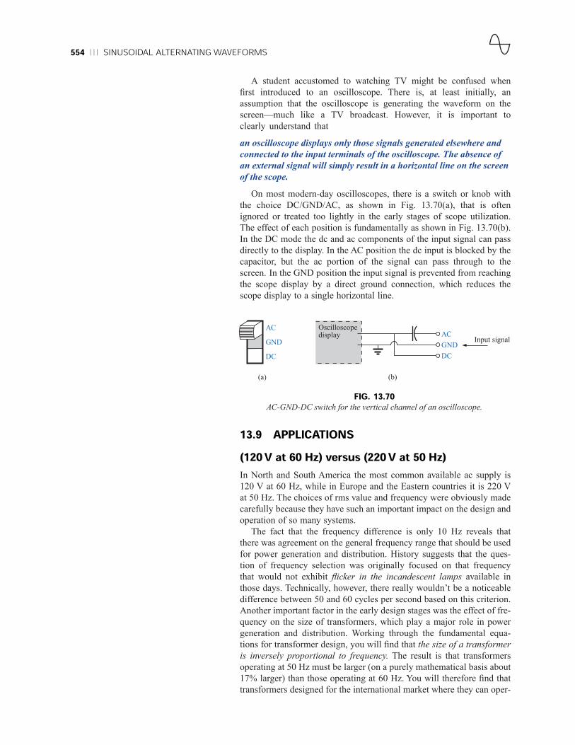
On most modern-day oscilloscopes, there is a switch or knob with
the choice DC/GND/AC, as shown in Fig. 13.70(a), that is often
ignored or treated too lightly in the early stages of scope utilization.
The effect of each position is fundamentally as shown in Fig. 13.70(b).
In the DC mode the dc and ac components of the input signal can pass
directly to the display. In the AC position the dc input is blocked by the
capacitor, but the ac portion of the signal can pass through to the
screen. In the GND position the input signal is prevented from reaching
the scope display by a direct ground connection, which reduces the
scope display to a single horizontal line.
Input signalAC
GND
DC
(b)
Oscilloscopedisplay
AC
GND
DC
(a)
FIG. 13.70AC-GND-DC switch for the vertical channel of an oscilloscope.
13.9 APPLICATIONS(120 V at 60 Hz) versus (220 V at 50 Hz)In North and South America the most common available ac supply is
120 V at 60 Hz, while in Europe and the Eastern countries it is 220 V
at 50 Hz. The choices of rms value and frequency were obviously made
carefully because they have such an important impact on the design and
operation of so many systems.
The fact that the frequency difference is only 10 Hz reveals that
there was agreement on the general frequency range that should be used
for power generation and distribution. History suggests that the ques-
tion of frequency selection was originally focused on that frequency
that would not exhibit flicker in the incandescent lamps available in
those days. Technically, however, there really wouldn’t be a noticeable
difference between 50 and 60 cycles per second based on this criterion.
Another important factor in the early design stages was the effect of fre-
quency on the size of transformers, which play a major role in power
generation and distribution. Working through the fundamental equa-
tions for transformer design, you will find that the size of a transformer
is inversely proportional to frequency. The result is that transformers
operating at 50 Hz must be larger (on a purely mathematical basis about
17% larger) than those operating at 60 Hz. You will therefore find that
transformers designed for the international market where they can oper-

APPLICATIONS 555
ate on 50 Hz or 60 Hz are designed around the 50-Hz frequency. On the
other side of the coin, however, higher frequencies result in increased
concerns about arcing, increased losses in the transformer core due to
eddy current and hysteresis losses (Chapter 19), and skin effect phe-
nomena (Chapter 19). Somewhere in the discussion we must consider
the fact that 60 Hz is an exact multiple of 60 seconds in a minute and
60 minutes in an hour. Since accurate timing is such a critical part of
our technological design, was this a significant motive in the final
choice? There is also the question about whether the 50 Hz is a result
of the close affinity of this value to the metric system. Keep in mind
that powers of 10 are all powerful in the metric system, with 100 cm in
a meter, 100°C the boiling point of water, and so on. Note that 50 Hz is
exactly half of this special number. All in all, it would seem that both
sides have an argument that would be worth defending. However, in the
final analysis, we must also wonder whether the difference is simply
political in nature.
The difference in voltage between North America and Europe is a
different matter entirely in the sense that the difference is close to
100%. Again, however, there are valid arguments for both sides. There
is no question that larger voltages such as 220 V raise safety issues
beyond those raised by voltages of 120 V. However, when higher volt-
ages are supplied, there is less current in the wire for the same power
demand, permitting the use of smaller conductors—a real money saver.
In addition, motors, compressors, and so on, found in common home
appliances and throughout the industrial community can be smaller in
size. Higher voltages, however, also bring back the concern about arc-
ing effects, insulation requirements, and, due to real safety concerns,
higher installation costs. In general, however, international travelers are
prepared for most situations if they have a transformer that can convert
from their home level to that of the country they plan to visit. Most
equipment (not clocks, of course) can run quite well on 50 Hz or 60 Hz
for most travel periods. For any unit not operating at its design fre-
quency, it will simply have to “work a little harder” to perform the
given task. The major problem for the traveler is not the transformer
itself but the wide variety of plugs used from one country to another.
Each country has its own design for the “female” plug in the wall. For
the three-week tour, this could mean as many as 6 to 10 different plugs
of the type shown in Fig. 13.71. For a 120-V, 60-Hz supply, the plug is
quite standard in appearance with its two spade leads (and possible
ground connection).
In any event, both the 120 V at 60 Hz and the 220 V at 50 Hz are
obviously meeting the needs of the consumer. It is a debate that could
go on at length without an ultimate victor.
Safety Concerns (High Voltages and dc versus ac)Be aware that any “live” network should be treated with a calculated
level of respect. Electricity in its various forms is not to be feared but
should be employed with some awareness of its potentially dangerous
side effects. It is common knowledge that electricity and water do not
mix (never use extension cords or plug in TVs or radios in the bath-
room) because a full 120 V in a layer of water of any height (from a
shallow puddle to a full bath) can be lethal. However, other effects of
dc and ac voltages are less known. In general, as the voltage and cur-
rent increase, your concern about safety should increase exponentially.
FIG. 13.71Variety of plugs for a 220-V, 50-Hz
connection.

556 SINUSOIDAL ALTERNATING WAVEFORMS
For instance, under dry conditions, most human beings can survive a
120-V ac shock such as obtained when changing a light bulb, turning
on a switch, and so on. Most electricians have experienced such a jolt
many times in their careers. However, ask an electrician to relate how it
feels to hit 220 V, and the response (if he or she has been unfortunate to
have had such an experience) will be totally different. How often have
you heard of a back-hoe operator hitting a 220-V line and having a fatal
heart attack? Remember, the operator is sitting in a metal container on
a damp ground which provides an excellent path for the resulting cur-
rent to flow from the line to ground. If only for a short period of time,
with the best environment (rubber-sole shoes, etc.), in a situation where
you can quickly escape the situation, most human beings can also sur-
vive a 220-V shock. However, as mentioned above, it is one you will
not quickly forget. For voltages beyond 220 V rms, the chances of sur-
vival go down exponentially with increase in voltage. It takes only
about 10 mA of steady current through the heart to put it in defibrilla-
tion. In general, therefore, always be sure that the power is discon-
nected when working on the repair of electrical equipment. Don’t
assume that throwing a wall switch will disconnect the power. Throw
the main circuit breaker and test the lines with a voltmeter before work-
ing on the system. Since voltage is a two-point phenomenon, don’t be a
hero and work with one line at at time—accidents happen!
You should also be aware that the reaction to dc voltages is quite dif-
ferent from that to ac voltages. You have probably seen in movies or
comic strips that people are often unable to let go of a hot wire. This is
evidence of the most important difference between the two types of
voltages. As mentioned above, if you happen to touch a “hot” 120-V ac
line, you will probably get a good sting, but you can let go. If it hap-
pens to be a “hot” 120-V dc line, you will probably not be able to let
go, and a fatality could occur. Time plays an important role when this
happens, because the longer you are subjected to the dc voltage, the
more the resistance in the body decreases until a fatal current can be
established. The reason that we can let go of an ac line is best demon-
strated by carefully examining the 120-V rms, 60-Hz voltage in Fig.
13.72. Since the voltage is oscillating, there is a period of time when the
voltage is near zero or less than, say, 20 V, and is reversing in direction.
Although this time interval is very short, it appears every 8.3 ms and
provides a window to let go.
Now that we are aware of the additional dangers of dc voltages, it is
important to mention that under the wrong conditions, dc voltages as
low as 12 V such as from a car battery can be quite dangerous. If you
happen to be working on a car under wet conditions, or if you are
sweating badly for some reason or, worse yet, wearing a wedding ring
that may have moisture and body salt underneath, touching the positive
terminal may initiate the process whereby the body resistance begins to
drop and serious injury could take place. It is one of the reasons you
seldom see a professional electrician wearing any rings or jewelry—it
is just not worth the risk.
Before leaving this topic of safety concerns, you should also be
aware of the dangers of high-frequency supplies. We are all aware of
what 2.45 GHz at 120 V can do to a meat product in a microwave oven.
As discussed in Chapter 5, it is therefore very important that the seal
around the oven be as tight as possible. However, don’t ever assume
that anything is absolutely perfect in design—so don’t make it a habit
to view the cooking process in the microwave 6 in. from the door on a
V(volts)
tf
120 V rmsac voltage
t
170
200
–20
FIG 13.72Interval of time when sinusoidal voltage is
near zero volts.
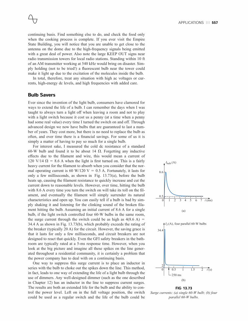
APPLICATIONS 557
continuing basis. Find something else to do, and check the food only
when the cooking process is complete. If you ever visit the Empire
State Building, you will notice that you are unable to get close to the
antenna on the dome due to the high-frequency signals being emitted
with a great deal of power. Also note the large KEEP OUT signs near
radio transmission towers for local radio stations. Standing within 10 ft
of an AM transmitter working at 540 kHz would bring on disaster. Sim-
ply holding (not to be tried!) a fluorescent bulb near the tower could
make it light up due to the excitation of the molecules inside the bulb.
In total, therefore, treat any situation with high ac voltages or cur-
rents, high-energy dc levels, and high frequencies with added care.
Bulb SaversEver since the invention of the light bulb, consumers have clamored for
ways to extend the life of a bulb. I can remember the days when I was
taught to always turn a light off when leaving a room and not to play
with a light switch because it cost us a penny (at a time when a penny
had some real value) every time I turned the switch on and off. Through
advanced design we now have bulbs that are guaranteed to last a num-
ber of years. They cost more, but there is no need to replace the bulb as
often, and over time there is a financial savings. For some of us it is
simply a matter of having to pay so much for a single bulb.
For interest sake, I measured the cold dc resistance of a standard
60-W bulb and found it to be about 14 V. Forgetting any inductive
effects due to the filament and wire, this would mean a current of
120 V/14 V 5 8.6 A when the light is first turned on. This is a fairly
heavy current for the filament to absorb when you consider that the nor-
mal operating current is 60 W/120 V 5 0.5 A. Fortunately, it lasts for
only a few milliseconds, as shown in Fig. 13.73(a), before the bulb
heats up, causing the filament resistance to quickly increase and cut the
current down to reasonable levels. However, over time, hitting the bulb
with 8.6 A every time you turn the switch on will take its toll on the fil-
ament, and eventually the filament will simply surrender its natural
characteristics and open up. You can easily tell if a bulb is bad by sim-
ply shaking it and listening for the clinking sound of the broken fila-
ment hitting the bulb. Assuming an initial current of 8.6 A for a single
bulb, if the light switch controlled four 60-W bulbs in the same room,
the surge current through the switch could be as high as 4(8.6 A) 5
34.4 A as shown in Fig. 13.73(b), which probably exceeds the rating of
the breaker (typically 20 A) for the circuit. However, the saving grace is
that it lasts for only a few milliseconds, and circuit breakers are not
designed to react that quickly. Even the GFI safety breakers in the bath-
room are typically rated at a 5-ms response time. However, when you
look at the big picture and imagine all these spikes on the line gener-
ated throughout a residential community, it is certainly a problem that
the power company has to deal with on a continuing basis.
One way to suppress this surge current is to place an inductor in
series with the bulb to choke out the spikes down the line. This method,
in fact, leads to one way of extending the life of a light bulb through the
use of dimmers. Any well-designed dimmer (such as the one described
in Chapter 12) has an inductor in the line to suppress current surges.
The results are both an extended life for the bulb and the ability to con-
trol the power level. Left on in the full voltage position, the switch
could be used as a regular switch and the life of the bulb could be
0 0.5 1 1.5 2 t (s)
2
34.4
IT (A), four parallel 60-W bulbs
(b)
250 ms
(a)
Ibulb (A)
8.6
0.5
0 1 2 3 4 5 6 7 t (ms)
FIG 13.73Surge currents: (a) single 60-W bulb; (b) four
parallel 60-W bulbs.

558 SINUSOIDAL ALTERNATING WAVEFORMS
extended. In fact, many dimmers now use triacs designed to turn on
only when the applied voltage passes through zero. If we look at the full
sine wave of Fig. 13.74(a), we find that the voltage is at least half of its
maximum value of 85 V for a full two-thirds of each cycle, or about
67% of the time. The chances, therefore, of your turning on a light bulb
with at least 85 V on the line is far better than 2 to 1, so you can expect
the current for a 60-W light bulb to be at least 85 V/14 V 5 6 A 67%
of the time, which exceeds the rated 0.5-A rated value by 1100%. If we
use a dimmer with a triac designed to turn on only when the applied
voltage passes through zero or shortly thereafter, as shown in Fig.
(a)
170
85
–85
–170
0
V (volts)
120°
30° 150°
360°180°
θ
120 V rmsac voltage
(b)
170
85
–85
–170
0
Vapplied
V (volts)
Vbulb 360°180°90° t
Turn-onDimmer ensuresbulb will notturn on whenapplied voltage isnear its maximum.
FIG. 13.74Turn-on voltage: (a) equal to or greater than one-half the peak value; (b) when
a dimmer is used.
Id
High resistance
Lowresistance
High resistance(diode open circuit)
Vd
Vd
Id
+ –
0
(c)
+0.7 V – +0.7 VIlamp(for positive regionof applied voltage)
Open circuits forpositive region ofapplied voltage
+
120-V rms line
Lamp168.6 V
+
––
Return
170 Vpeak
(b)
(a)
FIG. 13.75Bulb saver: (a) external appearance; (b) basic operation; (c) diode
characteristics at high current levels.

COMPUTER ANALYSIS 559
13.74(b), the applied voltage will increase from about zero volts, giving
the bulb time to warm up before the full voltage is applied.
Another commercial offering to extend the life of light bulbs is the
smaller circular disc shown in Fig. 13.75(a) which is inserted between
the bulb and the holder. Contacts are provided on both sides to permit
conduction through the simple diode network shown in Fig. 13.75(b).
You may recall from an earlier chapter that the voltage across diodes in
the on state is 0.7 V as shown for each diode in Fig. 13.75(b) for the
positive portion of the input voltage. The result is that the voltage to the
bulb is reduced by about 1.4 V throughout the cycle, reducing the
power delivered to the bulb. For most situations the reduced lighting is
not a problem, and the bulb will last longer simply because it is not
pressed to work at full output. However, the real saving in the device is
the manner in which it could help suppress the surge currents through
the light bulb. The true characteristics of a diode are shown in Fig.
13.75(c) for the full range of currents through the diode. For most
applications in electronic circuits, the vertical region is employed. For
excessive currents the diode characteristics flatten out as shown. This
region is characterized as having a large resistance (compared to very
small resistance of the vertical region) which will come into play
when the bulb is first turned on. In other words, when the bulb is first
turned on, the current will be so high that the diode will enter its high-
resistance region and by Ohm’s law will limit the surge current—
thereby extending the life of the bulb. The two diodes facing the other
way are for the negative portion of the supply voltage.
New methods of extending the life of bulbs hit the marketplace every
day. All in all, however, one guaranteed way to extend the life of your
bulbs is to return to the old philosophy of turning lights off when you
leave a room, and “Don’t play with the light switch!”
13.10 COMPUTER ANALYSISPSpiceOrCAD Capture offers a variety of ac voltage and current sources.
However, for the purposes of this text, the voltage source VSIN and
the current source ISIN are the most appropriate because they have a
list of attributes that will cover current areas of interest. Under the
library SOURCE, a number of others are listed, but they don’t have
the full range of the above, or they are dedicated to only one type of
analysis. On occasion, ISRC will be used because it has an arrow
symbol like that appearing in the text, and it can be used for dc, ac,
and some transient analyses. The symbol for ISIN is simply a sine
wave which utilizes the plus-and-minus sign to indicate direction. The
sources VAC, IAC, VSRC, and ISRC are fine if the magnitude and
the phase of a specific quantity are desired or if a transient plot against
frequency is desired. However, they will not provide a transient
response against time even if the frequency and the transient informa-
tion are provided for the simulation.
For all of the sinusoidal sources, the magnitude (VAMPL) is the
peak value of the waveform and not the rms value. This will become
clear when a plot of a quantity is desired and the magnitude calculated
by PSpice is the peak value of the transient response. However, for a
purely steady-state ac response, the magnitude provided can be the rms

560 SINUSOIDAL ALTERNATING WAVEFORMS
value, and the output read as the rms value. Only when a plot is desired
will it be clear that PSpice is accepting every ac magnitude as the peak
value of the waveform. Of course, the phase angle is the same whether
the magnitude is the peak or the rms value.
Before examining the mechanics of getting the various sources,
remember that
Transient Analysis provides an ac or a dc output versus time, while
AC Sweep is used to obtain a plot versus frequency.
To obtain any of the sources listed above, apply the following sequence:
Place part key-Place Part dialog box-Source-(enter type of source).
Once selected the ac source VSIN will appear on the schematic with
VOFF, VAMPL, and FREQ. Always specify VOFF as 0 V (unless a
specific value is part of the analysis), and provide a value for the ampli-
tude and frequency. The remaining quantities of PHASE, AC, DC, DF,
and TD can be entered by double-clicking on the source symbol to
obtain the Property Editor, although PHASE, DF (damping factor),
and TD (time delay) do have a default of 0 s. To add a phase angle, sim-
ply click on PHASE, enter the phase angle in the box below, and then
select Apply. If you want to display a factor such as a phase angle of
60°, simply click on PHASE followed by Display to obtain the Dis-
play Properties dialog box. Then choose Name and Value followed by
OK and Apply, and leave the Properties Editor dialog box (X) to see
PHASE560 next to the VSIN source. The next chapter will include the
use of the ac source in a simple circuit.
Electronics WorkbenchFor EWB, the ac voltage source is available from two sources—the
Sources parts bin and the Function Generator. The major difference
between the two is that the phase angle can be set when using the Sources
parts bin, whereas it cannot be set using the Function Generator.
Under Sources, the ac voltage source is the fourth option down on
the left column of the toolbar. When selected and placed, it will display
the default values for the amplitude, frequency, and phase.All the param-
eters of the source can be changed by double-clicking on the source
symbol to obtain the AC Voltage dialog box. The Voltage Amplitude
and Voltage RMS are interlinked so that when you change one, the
other will change accordingly. For the 1V default value, the rms value
is automatically listed as 0.71 (not 0.7071 because of the hundredths-
place accuracy). Note that the unit of measurement is controlled by the
scrolls to the right of the default label and cannot be set by typing in the
desired unit of measurement. The label can be changed by simply
switching the Label heading and inserting the desired label. After all
the changes have been made in the AC Voltage dialog box, click OK,
and all the changes will appear next to the ac voltage source symbol. In
Fig. 13.76 the label was changed to Vs and the amplitude to 10 V while
the frequency and phase angle were left with their default values. It is
particularly important to realize that
for any frequency analysis (that is, where the frequency will change),
the AC Magnitude of the ac source must be set under Analysis Setup
in the AC Voltage dialog box. Failure to do so will create results
linked to the default values rather than the value set under the Value
heading.

COMPUTER ANALYSIS 561
To view the sinusoidal voltage set in Fig. 13.76, an oscilloscope can
be selected from the Instrument toolbar at the right of the screen. It is
the fourth option down and has the appearance shown in Fig. 13.76
when selected. Note that it is a dual-channel oscilloscope with an A
channel and a B channel. It has a ground (G) connection and a trigger
(T) connection. The connections for viewing the ac voltage source on
the A channel are provided in Fig. 13.76. Note that the trigger control
is also connected to the A channel for sync control. The screen appear-
ing in Fig. 13.76 can be displayed by double-clicking on the oscillo-
scope symbol on the screen. It has all the major controls of a typical
laboratory oscilloscope. When you select Simulate-Run or select 1 on
the Simulate Switch, the ac voltage will appear on the screen. Chang-
ing the Time base to 100 ms/div. will result in the display of Fig. 13.76
since there are 10 divisions across the screen and 10(100ms) 5 1 ms
(the period of the applied signal). Changes in the Time base are made
by simply clicking on the default value to obtain the scrolls in the same
box. It is important to remember, however, that
changes in the oscilloscope setting or any network should not be
made until the simulation is ended by disabling the Simulate-Run
option or placing the Simulate switch in the 0 mode.
The options within the time base are set by the scroll bars and can-
not be changed—again they match those typically available on a labo-
ratory oscilloscope. The vertical sensitivity of the A channel was auto-
matically set by the program at 5 V/div. to result in two vertical boxes
for the peak value as shown in Fig. 13.76. Note the AC and DC key
pads below Channel A. Since there is no dc component in the applied
signal, either one will result in the same display. The Trigger control is
FIG. 13.76Using the oscilloscope to display the sinusoidal ac voltage source available in
the Electronics Workbench Sources tool bin.

562 SINUSOIDAL ALTERNATING WAVEFORMS
set on the positive transition at a level of 0 V. The T1 and T2 refer to
the cursor positions on the horizontal time axis. By simply clicking on
the small red triangle at the top of the red line at the far left edge of the
screen and dragging the triangle, you can move the vertical red line to
any position along the axis. In Fig.13.76 it was moved to the peak value
of the waveform at 1⁄4 of the total period or 0.25 ms 5 250 ms. Note the
value of T1 (250.3 ms) and the corresponding value of VA1 (10.0V). By
moving the other cursor with a blue triangle at the top to 1⁄2 the total
period or 0.5 ms 5 500 ms, we find that the value at T2 (500.3 ms) is
218.9 mV (VA2), which is approximately 0 V for a waveform with a
peak value of 10 V. The accuracy is controlled by the number of data
points called for in the simulation setup. The more data points, the
higher the likelihood of a higher degree of accuracy for the desired
quantity. However, an increased number of data points will also extend
the running time of the simulation. The third display box to the right
gives the difference between T2 and T1 as 250 ms and difference
between their magnitudes (VA2-VA1) as 210 V, with the negative sign
appearing because VA1 is greater than VA2.
As mentioned above, an ac voltage can also be obtained from the
Function Generator appearing as the second option down on the
Instrument toolbar. Its symbol appears in Fig. 13.77 with positive, neg-
ative, and ground connections. Double-click on the generator graphic
symbol, and the Function Generator-XFG1 dialog box will appear in
which selections can be made. For this example, the sinusoidal wave-
form is chosen. The Frequency is set at 1 kHz, the Amplitude is set at
10 V, and the Offset is left at 0 V. Note that there is no option to set the
phase angle as was possible for the source above. Double-clicking on the
FIG. 13.77Using the function generator to place a sinusoidal ac voltage waveform on the
screen of the oscilloscope.

COMPUTER ANALYSIS 563
oscilloscope will generate the oscilloscope on which a Timebase of
100 ms/div. can be set again with a vertical sensitivity of 5 V/div. Select
1 on the Simulate switch, and the waveform of Fig. 13.77 will appear.
Choosing Singular under Trigger will result in a fixed display; then set
the Simulate switch on 0 to the end the simulation. Placing the cursors
in the same position shows that the waveforms for Figs. 13.76 and 13.77
are the same.
For most of the EWB analyses to appear in this text, the
AC–VOLTAGE–SOURCE under Sources will be employed. How-
ever, with such a limited introduction to EWB, it seemed appropriate
to introduce the use of the Function Generator because of its close
linkage to the laboratory experience.
C11
Calculating the Average Value of a Waveform The absence of
any network configurations to analyze in this chapter severely limits the
content with respect to packaged computer programs. However, the
door is still wide open for the application of a language to write pro-
grams that can be helpful in the application of some of the concepts
introduced in the chapter. In particular, let us examine the C11 pro-
gram of Fig. 13.78, designed to calculate the average value of a pulse
waveform having up to 5 different levels.
The program begins with a heading and preprocessor directive.
Recall that the iostream.h header file sets up the input-output path
Heading
Preprocessor
directive
Define
form
and
name
of
variables
Obtain
# of
levels
Iterative
for
statement
Calculate Vave
Display
results
Body
of
program
FIG. 13.78C11 program designed to calculate the average value of a waveform with up
to five positive or negative pulses.

564 SINUSOIDAL ALTERNATING WAVEFORMS
between the program and the disk operating system. Note that the main
( ) part of the program extends all the way down to the bottom, as iden-
tified by the braces . Within this region all the calculations will be
performed, and the results will be displayed.
Within the main ( ) part of the program, all the variables to be
employed in the calculations are defined as floating point (decimal val-
ues) or integer (whole numbers). The comments on the right identify
each variable. This is followed by a display of the question about how
many levels will be encountered in the waveform using cout (comment
out). The cin (comment in) statement permits a response from the user.
Next, the loop statement for is employed to establish a fixed number
of repetitions of the sequence appearing within the parentheses ( ) for
a number of loops defined by the variable levels. The format of this for
statement is such that the first entry within the parentheses ( ) is the
initial value of the variable count (1 in this case), followed by a semi-
colon and then a test expression determining how many times the
sequence to follow will be repeated. In other words, if levels is 5, then
the first pass through the for statement will result in 1 being compared
to 5, and the test expression will be satisfied because 5 is greater than
or equal to 1 (< 5). On the next pass, count will be increased to 2, and
the same test will be performed. Eventually count will equal 5, the test
expression will not be satisfied, and the program will move to its next
statement, which is Vave 5 VT sum/ T. The last entry count11 of the
for statement simply increments the variable count after each iteration.
The first line within the for statement calls for a line to be skipped, fol-
lowed by a question on the display about the level of voltage for the
first time interval. The question will include the current state of the
count variable followed by a colon. In C11 all character outputs must
be displayed in quotes (not required for numerical values). However,
note the absence of the quotes for count since it will be a numerical
value. Next the user enters the first voltage level through cin, followed
by a request for the time interval. In this case units are not provided but
simply measured as an increment of the whole; that is, if the total
period is 5 ms and the first interval is 2 ms, then just a 2 is entered.
The area under the pulse is then calculated to establish the variable
VTsum, which was initially set at 0. On the next pass the value of
VTsum will be the value obtained by the first run plus the new area. In
other words, VTsum is a storage for the total accumulated area. Simi-
larly, T is the accumulated sum of the time intervals.
Following a FALSE response from the test expression of the for
statement, the program will move to calculate the average value of the
waveform using the accumulated values of the area and time. A line is
then skipped; and the average value is displayed with the remaining
cout statements. Brackets have been added along the edge of the pro-
gram to help identify the various components of the program.
A program is now available that can find the average value of any
pulse waveform having up to five positive or negative pulses. It can be
placed in storage and simply called for when needed. Operations such as
the above are not available in either form of PSpice or in any commer-
cially available software package. It took the knowledge of a language
and a few minutes of time to generate a short program of lifetime value.
Two runs will clearly reveal what will be displayed and how the out-
put will appear. The waveform of Fig. 13.79 has five levels, entered as
shown in the output file of Fig. 13.80. As indicated the average value is
1.6 V. The waveform of Fig. 13.81 has only three pulses, and the time
0
–3 V
1 2 3 4 t (ms)
v
5
8 V
4 V
–1 V
T
0 V
FIG. 13.79Waveform with five pulses to be analyzed by
the C11 program of Fig. 13.78.
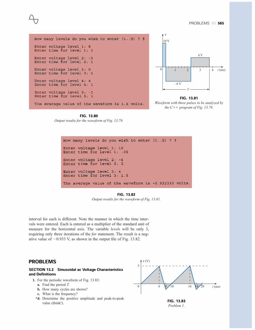
PROBLEMS 565
interval for each is different. Note the manner in which the time inter-
vals were entered. Each is entered as a multiplier of the standard unit of
measure for the horizontal axis. The variable levels will be only 3,
requiring only three iterations of the for statement. The result is a neg-
ative value of 20.933 V, as shown in the output file of Fig. 13.82.
0
–6 V
1 2 3 t (ms)
v
4
10 V
4 V
T
FIG. 13.81Waveform with three pulses to be analyzed by
the C11 program of Fig. 13.78.
FIG. 13.80Output results for the waveform of Fig. 13.79.
FIG. 13.82Output results for the waveform of Fig. 13.81.
PROBLEMSSECTION 13.2 Sinusoidal ac Voltage Characteristicsand Definitions
1. For the periodic waveform of Fig. 13.83:
a. Find the period T.
b. How many cycles are shown?
c. What is the frequency?
*d. Determine the positive amplitude and peak-to-peak
value (think!).
v (V)
5
0 6 8 10 16 18 20 t (ms)
FIG. 13.83Problem 1.

566 SINUSOIDAL ALTERNATING WAVEFORMS
2. Repeat Problem 1 for the periodic waveform of Fig.
13.84.
0 5 10 15 20 25 30 35t (ms)
10
–10
v (V)
FIG. 13.84Problems 2, 9, and 47.
3. Determine the period and frequency of the sawtooth
waveform of Fig. 13.85.
36261660
20
v (V)
t (ms)
FIG. 13.85Problems 3 and 48.
4. Find the period of a periodic waveform whose frequency is
a. 25 Hz. b. 35 MHz.
c. 55 kHz. d. 1 Hz.
5. Find the frequency of a repeating waveform whose
period is
a. 1/60 s. b. 0.01 s.
c. 34 ms. d. 25 ms.
6. Find the period of a sinusoidal waveform that completes
80 cycles in 24 ms.
7. If a periodic waveform has a frequency of 20 Hz, how
long (in seconds) will it take to complete five cycles?
8. What is the frequency of a periodic waveform that com-
pletes 42 cycles in 6 s?
9. Sketch a periodic square wave like that appearing in Fig.
13.84 with a frequency of 20,000 Hz and a peak value of
10 mV.
10. For the oscilloscope pattern of Fig. 13.86:
a. Determine the peak amplitude.
b. Find the period.
c. Calculate the frequency.
Redraw the oscilloscope pattern if a 125-mV dc level
were added to the input waveform.
Vertical sensitivity = 50 mV/div.Horizontal sensitivity = 10 s/div.m
FIG. 13.86Problem 10.

PROBLEMS 567
SECTION 13.3 The Sine Wave11. Convert the following degrees to radians:
a. 45° b. 60°
c. 120° d. 270°
e. 178° f. 221°
12. Convert the following radians to degrees:
a. p/4 b. p/6
c. 1
1
0p d.
7
6p
e. 3p f. 0.55p
13. Find the angular velocity of a waveform with a period of
a. 2 s. b. 0.3 ms.
c. 4 ms. d. 2
1
6 s.
14. Find the angular velocity of a waveform with a frequency
of
a. 50 Hz. b. 600 Hz.
c. 2 kHz. d. 0.004 MHz.
15. Find the frequency and period of sine waves having an
angular velocity of
a. 754 rad/s. b. 8.4 rad/s.
c. 6000 rad/s. d. 1
1
6 rad/s.
16. Given f 5 60 Hz, determine how long it will take the
sinusoidal waveform to pass through an angle of 45°.
17. If a sinusoidal waveform passes through an angle of 30°
in 5 ms, determine the angular velocity of the waveform.
SECTION 13.4 General Format for the SinusoidalVoltage or Current18. Find the amplitude and frequency of the following
waves:
a. 20 sin 377t b. 5 sin 754t
c. 106 sin 10,000t d. 0.001 sin 942t
e. 27.6 sin 43.6t f. (4
1
2) sin 6.283t
19. Sketch 5 sin 754t with the abscissa
a. angle in degrees.
b. angle in radians.
c. time in seconds.
20. Sketch 106 sin 10,000t with the abscissa
a. angle in degrees.
b. angle in radians.
c. time in seconds.
21. Sketch 27.6 sin 43.6t with the abscissa
a. angle in degrees.
b. angle in radians.
c. time in seconds.
22. If e 5 300 sin 157t, how long (in seconds) does it take
this waveform to complete 1/2 cycle?
23. Given i 5 0.5 sin a, determine i at a 5 72°.
24. Given v 5 20 sin a, determine v at a 5 1.2p.
*25. Given v 5 30 3 1023 sin a, determine the angles at
which v will be 6 mV.
*26. If v 5 40 V at a 5 30° and t 5 1 ms, determine the
mathematical expression for the sinusoidal voltage.

568 SINUSOIDAL ALTERNATING WAVEFORMS
SECTION 13.5 Phase Relations27. Sketch sin(377t 1 60°) with the abscissa
a. angle in degrees.
b. angle in radians.
c. time in seconds.
28. Sketch the following waveforms:
a. 50 sin(qt 1 0°) b. 220 sin(qt 1 2°)
c. 5 sin(qt 1 60°) d. 4 cos qt
e. 2 cos(qt 1 10°) f. 25 cos(qt 1 20°)
29. Find the phase relationship between the waveforms of
each set:
a. v 5 4 sin(qt 1 50°)
i 5 6 sin(qt 1 40°)
b. v 5 25 sin(qt 2 80°)
i 5 5 3 1023 sin(qt 2 10°)
c. v 5 0.2 sin(qt 2 60°)
i 5 0.1 sin(qt 1 20°)
d. v 5 200 sin(qt 2 210°)
i 5 25 sin(qt 2 60°)
*30. Repeat Problem 29 for the following sets:
a. v 5 2 cos(qt 2 30°) b. v 5 21 sin(qt 1 20°)
i 5 5 sin(qt 1 60°) i 5 10 sin(qt 2 70°)
c. v 5 24 cos(qt 1 90°)
i 5 22 sin(qt 1 10°)
31. Write the analytical expression for the waveforms of Fig.
13.87 with the phase angle in degrees.
v (V)
qt0
p6
25 f = 60 Hz
i (A)
qt0
–3 × 10⁻³
f = 1000 Hz
23p
(b)(a)
FIG. 13.87Problem 31.
32. Repeat Problem 31 for the waveforms of Fig. 13.88.
p
v (V)
qt0
0.01 f = 25 Hz
i (A)
vt0
2 × 10⁻³
f = 10 kHz
34
1118
p
(a) (b)
FIG. 13.88Problem 32.

PROBLEMS 569
*33. The sinusoidal voltage v 5 200 sin(2p1000t 1 60°) is
plotted in Fig. 13.89. Determine the time t1.
*34. The sinusoidal current i 5 4 sin(50,000t 2 40°) is plot-
ted in Fig. 13.90. Determine the time t1.
200
t1–p 0 p 2p t
60°
t1
v
FIG. 13.89Problem 33.
4A
t1–p 0 p 2p t (ms)
40°
i
FIG. 13.90Problem 34.
*35. Determine the phase delay in milliseconds between the
following two waveforms:
v 5 60 sin(1800t 1 20°)
i 5 1.2 sin(1800t 2 20°)
36. For the oscilloscope display of Fig. 13.91:
a. Determine the period of each waveform.
b. Determine the frequency of each waveform.
c. Find the rms value of each waveform.
d. Determine the phase shift between the two waveforms
and which leads or lags.Vertical sensitivity = 0.5 V/div.Horizontal sensitivity = 1 ms/div.
e i
FIG. 13.91Problem 36.
Vertical sensitivity = 10 mV/div.Horizontal sensitivity = 0.2 ms/div.
FIG. 13.92Problem 37.
SECTION 13.6 Average Value37. For the waveform of Fig. 13.92:
a. Determine the period.
b. Find the frequency.
c. Determine the average value.
d. Sketch the resulting oscilloscope display if the verti-
cal channel is switched from DC to AC.

570 SINUSOIDAL ALTERNATING WAVEFORMS
38. Find the average value of the periodic waveforms of Fig.
13.93 over one full cycle.
1
1 cycle
0 2 3 t (s)
v (V)
–3
3
6
0 4 6 t (ms)
i (mA)
–8
20
8
(a) (b)
FIG. 13.93Problem 38.
39. Find the average value of the periodic waveforms of Fig.
13.94 over one full cycle.
10
v (V)
5
0
–5
–10
1 2 3 4 5 6 7 8 9 10 t (s)
1 cycle
(a)
10
5
0–5
–10
qtp
4
p
2
p 3
2p 2p
–15
(b)
1 cycle
Sine wave
i (mA)
FIG. 13.94Problem 39.
*40. a. By the method of approximation, using familiar geo-
metric shapes, find the area under the curve of Fig.
13.95 from zero to 10 s. Compare your solution with
the actual area of 5 volt-seconds (V• s).
b. Find the average value of the waveform from zero to
10 s.
0
0.632
1 2 3 4 5 6 7 8 9 10 t (s)
0.0070.019
0.049
0.135
0.368
0.993
v = e–t0.981
0.951
0.865
v = 1 – e–t
v (V)
1
FIG. 13.95Problem 40.

PROBLEMS 571
*41. For the waveform of Fig. 13.96:
a. Determine the period.
b. Find the frequency.
c. Determine the average value.
d. Sketch the resulting oscilloscope display if the verti-
cal channel is switched from DC to AC.
0
1 cycle
1 2 3 4 5 6 7 8 9 10 11 12 t (s)
v (V)
3
2
1
–1
–2
FIG. 13.97Problem 44.
0
1 cycle
1 2 3 4 5 6 7 8 9 10 11 12 t (s)
v (V)
3
2
1
–1
–2
–3
FIG. 13.98Problem 45.
0 4 8
–10
10
v (V)
1 cycle
t (ms)
FIG. 13.99Problem 46.
Vertical sensitivity = 10 mV/div.Horizontal sensitivity = 10 s/div. m
FIG. 13.96Problem 41.SECTION 13.7 Effective (rms) Values
42. Find the rms values of the following sinusoidal wave-
forms:
a. v 5 20 sin 754t
b. v 5 7.07 sin 377t
c. i 5 0.006 sin(400t 1 20°)
d. i 5 16 3 1023 sin(377t 2 10°)
43. Write the sinusoidal expressions for voltages and cur-
rents having the following rms values at a frequency of
60 Hz with zero phase shift:
a. 1.414 V b. 70.7 V
c. 0.06 A d. 24 mA
44. Find the rms value of the periodic waveform of Fig.
13.97 over one full cycle.
45. Find the rms value of the periodic waveform of Fig.
13.98 over one full cycle.
46. What are the average and rms values of the square wave
of Fig. 13.99?
47. What are the average and rms values of the waveform of
Fig. 13.84?
48. What is the average value of the waveform of Fig. 13.85?

572 SINUSOIDAL ALTERNATING WAVEFORMS
49. For each waveform of Fig. 13.100, determine the period,
frequency, average value, and rms value.
SECTION 13.8 ac Meters and Instruments50. Determine the reading of the meter for each situation of
Fig. 13.101.
Vertical sensitivity = 0.2 V/div.Horizontal sensitivity = 50 ms/div.m
Vertical sensitivity = 20 mV/div.Horizontal sensitivity = 10 ms/div.m
(b)(a)
Vertical sensitivity = 20 mV/div.Horizontal sensitivity = 10 ms/div.m
FIG. 13.100Problem 49.
d’Arsonval movement
2 kV
rms scale(half-waverectifier)
Voltmeter
(a)
+
–
Idc = 4 mA
v = 16 sin(377t + 20°)
+
–
ac
(b)
FIG. 13.101Problem 50.
SECTION 13.10 Computer AnalysisProgramming Language (C11, QBASIC, Pascal, etc.)
51. Given a sinusoidal function, write a program to deter-
mine the rms value, frequency, and period.
52. Given two sinusoidal functions, write a program to deter-
mine the phase shift between the two waveforms, and
indicate which is leading or lagging.
53. Given an alternating pulse waveform, write a program to
determine the average and rms values of the waveform
over one complete cycle.
Angular velocity The velocity with which a radius vector
projecting a sinusoidal function rotates about its center.
Average value The level of a waveform defined by the con-
dition that the area enclosed by the curve above this level is
exactly equal to the area enclosed by the curve below this
level.
GLOSSARYAlternating waveform A waveform that oscillates above
and below a defined reference level.
Amp-Clamp® A clamp-type instrument that will permit non-
invasive current measurements and that can be used as a con-
ventional voltmeter or ohmmeter.

GLOSSARY 573
Cycle A portion of a waveform contained in one period of time.
Effective value The equivalent dc value of any alternating
voltage or current.
Electrodynamometer meters Instruments that can measure
both ac and dc quantities without a change in internal cir-
cuitry.
Frequency ( f ) The number of cycles of a periodic waveform
that occur in 1 second.
Frequency counter An instrument that will provide a digital
display of the frequency or period of a periodic time-vary-
ing signal.
Instantaneous value The magnitude of a waveform at any
instant of time, denoted by lowercase letters.
Oscilloscope An instrument that will display, through the use
of a cathode-ray tube, the characteristics of a time-varying
signal.
Peak amplitude The maximum value of a waveform as mea-
sured from its average, or mean, value, denoted by upper-
case letters.
Peak-to-peak value The magnitude of the total swing of
a signal from positive to negative peaks. The sum of the
absolute values of the positive and negative peak values.
Peak value The maximum value of a waveform, denoted by
uppercase letters.
Period (T ) The time interval between successive repetitions
of a periodic waveform.
Periodic waveform A waveform that continually repeats
itself after a defined time interval.
Phase relationship An indication of which of two wave-
forms leads or lags the other, and by how many degrees or
radians.
Radian (rad) A unit of measure used to define a particular
segment of a circle. One radian is approximately equal to
57.3°; 2p rad are equal to 360°.
Root-mean-square (rms) value The root-mean-square or
effective value of a waveform.
Sinusoidal ac waveform An alternating waveform of unique
characteristics that oscillates with equal amplitude above
and below a given axis.
VOM A multimeter with the capability to measure resistance
and both ac and dc levels of current and voltage.
Waveform The path traced by a quantity, plotted as a func-
tion of some variable such as position, time, degrees, tem-
perature, and so on.


14
14.1 INTRODUCTIONThe response of the basic R, L, and C elements to a sinusoidal voltage
and current will be examined in this chapter, with special note of how
frequency will affect the “opposing” characteristic of each element.
Phasor notation will then be introduced to establish a method of analy-
sis that permits a direct correspondence with a number of the methods,
theorems, and concepts introduced in the dc chapters.
14.2 THE DERIVATIVEIn order to understand the response of the basic R, L, and C elements to
a sinusoidal signal, you need to examine the concept of the derivative
in some detail. It will not be necessary that you become proficient in the
mathematical technique, but simply that you understand the impact of a
relationship defined by a derivative.
Recall from Section 10.11 that the derivative dx/dt is defined as the
rate of change of x with respect to time. If x fails to change at a particu-
lar instant, dx 5 0, and the derivative is zero. For the sinusoidal wave-
form, dx/dt is zero only at the positive and negative peaks (qt 5 p/2 and
#sp in Fig. 14.1), since x fails to change at these instants of time. The
derivative dx/dt is actually the slope of the graph at any instant of time.
A close examination of the sinusoidal waveform will also indicate
that the greatest change in x will occur at the instants qt 5 0, p, and 2p.
The derivative is therefore a maximum at these points. At 0 and 2p, x
increases at its greatest rate, and the derivative is given a positive sign
since x increases with time. At p, dx/dt decreases at the same rate as it
increases at 0 and 2p, but the derivative is given a negative sign since x
decreases with time. Since the rate of change at 0, p, and 2p is the
same, the magnitude of the derivative at these points is the same also.
For various values of qt between these maxima and minima, the deriv-
ative will exist and will have values from the minimum to the maximum
inclusive. A plot of the derivative in Fig. 14.2 shows that
the derivative of a sine wave is a cosine wave.
u
The Basic Elements and Phasors
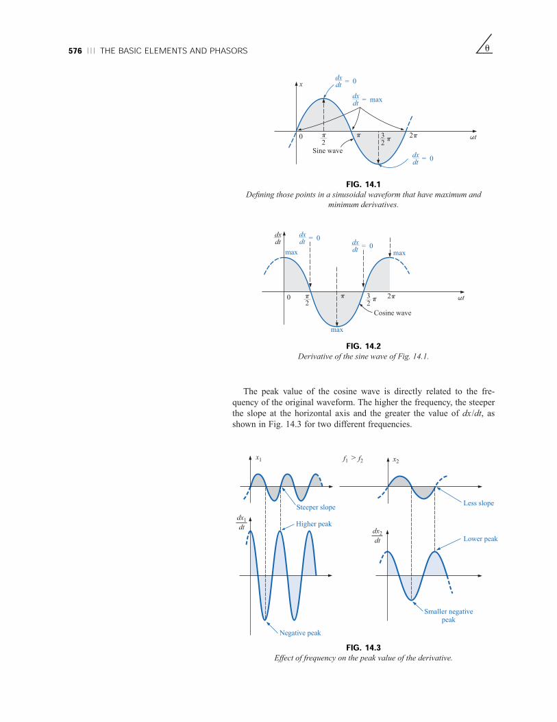
x1
Higher peak
Steeper slope
Negative peak
Lower peak
Less slope
Smaller negativepeak
x2f2f1 >
dx1
dtdx2
dt
576 THE BASIC ELEMENTS AND PHASORS u
FIG. 14.1Defining those points in a sinusoidal waveform that have maximum and
minimum derivatives.
Sine wave
qt0 p
dxdt
= 0
p 2p
dxdt
= max
dxdt
= 0
32
p
x
2p
Cosine wave
qt0 p2
dxdt
= 0
p 2p
dxdt
dxdt
= 0
max
max
32
p
max
FIG. 14.2Derivative of the sine wave of Fig. 14.1.
FIG. 14.3Effect of frequency on the peak value of the derivative.
The peak value of the cosine wave is directly related to the fre-
quency of the original waveform. The higher the frequency, the steeper
the slope at the horizontal axis and the greater the value of dx/dt, as
shown in Fig. 14.3 for two different frequencies.

u
Note in Fig. 14.3 that even though both waveforms (x1 and x2) have
the same peak value, the sinusoidal function with the higher frequency
produces the larger peak value for the derivative. In addition, note that
the derivative of a sine wave has the same period and frequency as
the original sinusoidal waveform.
For the sinusoidal voltage
e(t) 5 Em sin(qt 6 v)
the derivative can be found directly by differentiation (calculus) to pro-
duce the following:
e(t) 5 qEm cos(qt 6 v)
5 2pfEm cos(qt 6 v)(14.1)
The mechanics of the differentiation process will not be discussed or
investigated here; nor will they be required to continue with the text. Note,
however, that the peak value of the derivative, 2pfEm, is a function of the
frequency of e(t), and the derivative of a sine wave is a cosine wave.
14.3 RESPONSE OF BASIC R, L, AND CELEMENTS TO A SINUSOIDAL VOLTAGE OR CURRENTNow that we are familiar with the characteristics of the derivative of a
sinusoidal function, we can investigate the response of the basic ele-
ments R, L, and C to a sinusoidal voltage or current.
ResistorFor power-line frequencies and frequencies up to a few hundred kilo-
hertz, resistance is, for all practical purposes, unaffected by the fre-
quency of the applied sinusoidal voltage or current. For this frequency
region, the resistor R of Fig. 14.4 can be treated as a constant, and
Ohm’s law can be applied as follows. For v 5 Vm sin qt,
i 5 5 5 sin qt 5 Im sin qt
where (14.2)
In addition, for a given i,
v 5 iR 5 (Im sin qt)R 5 ImR sin qt 5 Vm sin qt
where (14.3)
A plot of v and i in Fig. 14.5 reveals that
for a purely resistive element, the voltage across and the current
through the element are in phase, with their peak values related by
Ohm’s law.
Vm 5 ImR
Im 5 V
R
m
VmR
Vm sin qt
R
vR
ddt
RESPONSE OF BASIC R, L, AND C ELEMENTS TO A SINUSOIDAL VOLTAGE OR CURRENT 577
v+
–
i
R
FIG. 14.4Determining the sinusoidal response for a
resistive element.
qt0 p 2p
iR
vR
Vm
Im
FIG. 14.5The voltage and current of a resistive element
are in phase.

e+–
vL+ –
L
Opposition afunction of f and L
iL
578 THE BASIC ELEMENTS AND PHASORS
InductorFor the series configuration of Fig. 14.6, the voltage velement of the
boxed-in element opposes the source e and thereby reduces the mag-
nitude of the current i. The magnitude of the voltage across the ele-
ment is determined by the opposition of the element to the flow of
charge, or current i. For a resistive element, we have found that the
opposition is its resistance and that velement and i are determined by
velement 5 iR.
We found in Chapter 12 that the voltage across an inductor is
directly related to the rate of change of current through the coil. Conse-
quently, the higher the frequency, the greater will be the rate of change
of current through the coil, and the greater the magnitude of the volt-
age. In addition, we found in the same chapter that the inductance of a
coil will determine the rate of change of the flux linking a coil for a par-
ticular change in current through the coil. The higher the inductance,
the greater the rate of change of the flux linkages, and the greater the
resulting voltage across the coil.
The inductive voltage, therefore, is directly related to the frequency
(or, more specifically, the angular velocity of the sinusoidal ac current
through the coil) and the inductance of the coil. For increasing values
of f and L in Fig. 14.7, the magnitude of vL will increase as described
above.
Utilizing the similarities between Figs. 14.6 and 14.7, we find that
increasing levels of vL are directly related to increasing levels of oppo-
sition in Fig. 14.6. Since vL will increase with both q (5 2pf ) and L,
the opposition of an inductive element is as defined in Fig. 14.7.
We will now verify some of the preceding conclusions using a more
mathematical approach and then define a few important quantities to be
employed in the sections and chapters to follow.
For the inductor of Fig. 14.8, we recall from Chapter 12 that
vL 5 L
and, applying differentiation,
5 (Im sin qt) 5 qIm cos qt
Therefore, vL 5 L 5 L(qIm cos qt) 5 qLIm cos qt
or vL 5 Vm sin(qt 1 90°)
where Vm 5 qLIm
Note that the peak value of vL is directly related to q (5 2pf ) and L
as predicted in the discussion above.
A plot of vL and iL in Fig. 14.9 reveals that
for an inductor, vL leads iL by 90°, or iL lags vL by 90°.
If a phase angle is included in the sinusoidal expression for iL, such
as
iL 5 Im sin(qt 6 v)
then vL 5 qLIm sin(qt 6 v 1 90°)
diLdt
ddt
diLdt
diLdt
u
Opposition
ei
+–+ –velement
FIG. 14.6Defining the opposition of an element to the
flow of charge through the element.
FIG. 14.7Defining the parameters that determine the
opposition of an inductive element to the flow
of charge.
iL = Im sin qt
L vL+
–
FIG. 14.8Investigating the sinusoidal response of an
inductive element.
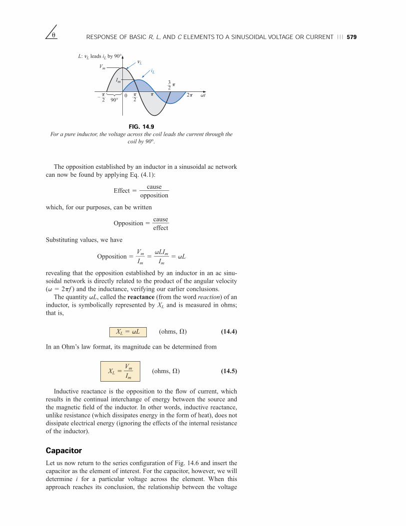
u
The opposition established by an inductor in a sinusoidal ac network
can now be found by applying Eq. (4.1):
Effect 5
which, for our purposes, can be written
Opposition 5
Substituting values, we have
Opposition 5 5 5 qL
revealing that the opposition established by an inductor in an ac sinu-
soidal network is directly related to the product of the angular velocity
(q 5 2pf ) and the inductance, verifying our earlier conclusions.
The quantity qL, called the reactance (from the word reaction) of an
inductor, is symbolically represented by XL and is measured in ohms;
that is,
(ohms, V) (14.4)
In an Ohm’s law format, its magnitude can be determined from
XL 5 (ohms, V) (14.5)
Inductive reactance is the opposition to the flow of current, which
results in the continual interchange of energy between the source and
the magnetic field of the inductor. In other words, inductive reactance,
unlike resistance (which dissipates energy in the form of heat), does not
dissipate electrical energy (ignoring the effects of the internal resistance
of the inductor).
CapacitorLet us now return to the series configuration of Fig. 14.6 and insert the
capacitor as the element of interest. For the capacitor, however, we will
determine i for a particular voltage across the element. When this
approach reaches its conclusion, the relationship between the voltage
VmIm
XL 5 qL
qLIm
Im
VmIm
causeeffect
causeopposition
RESPONSE OF BASIC R, L, AND C ELEMENTS TO A SINUSOIDAL VOLTAGE OR CURRENT 579
qt0 p 2p
iL
vLVm
Im
p2
32
p
–p
90°
L: vL leads iL by 90°
2
FIG. 14.9For a pure inductor, the voltage across the coil leads the current through the
coil by 90°.

580 THE BASIC ELEMENTS AND PHASORS
and current will be known, and the opposing voltage (velement) can be
determined for any sinusoidal current i.
Our investigation of the inductor revealed that the inductive voltage
across a coil opposes the instantaneous change in current through the
coil. For capacitive networks, the voltage across the capacitor is limited
by the rate at which charge can be deposited on, or released by, the
plates of the capacitor during the charging and discharging phases,
respectively. In other words, an instantaneous change in voltage across
a capacitor is opposed by the fact that there is an element of time
required to deposit charge on (or release charge from) the plates of a
capacitor, and V 5 Q/C.
Since capacitance is a measure of the rate at which a capacitor will
store charge on its plates,
for a particular change in voltage across the capacitor, the greater the
value of capacitance, the greater will be the resulting capacitive
current.
In addition, the fundamental equation relating the voltage across a
capacitor to the current of a capacitor [i 5 C(dv/dt)] indicates that
for a particular capacitance, the greater the rate of change of voltage
across the capacitor, the greater the capacitive current.
Certainly, an increase in frequency corresponds to an increase in the
rate of change of voltage across the capacitor and to an increase in the
current of the capacitor.
The current of a capacitor is therefore directly related to the fre-
quency (or, again more specifically, the angular velocity) and the capac-
itance of the capacitor. An increase in either quantity will result in an
increase in the current of the capacitor. For the basic configuration of
Fig. 14.10, however, we are interested in determining the opposition of
the capacitor as related to the resistance of a resistor and qL for the
inductor. Since an increase in current corresponds to a decrease in
opposition, and iC is proportional to q and C, the opposition of a capac-
itor is inversely related to q (5 2pf ) and C.
u
Opposition inverselyrelated to f and C
eiC+–
+ –vC
C
FIG. 14.10Defining the parameters that determine the opposition of a capacitive element
to the flow of the charge.
We will now verify, as we did for the inductor, some of the above
conclusions using a more mathematical approach.
For the capacitor of Fig. 14.11, we recall from Chapter 10 that
iC 5 C
and, applying differentiation,
5 (Vm sin qt) 5 qVm cos qtd
dt
dvCdt
dvCdt
iC = ?
vC = Vm sin qt
+
–C
FIG. 14.11Investigating the sinusoidal response of a
capacitive element.

u
Therefore,
iC 5 C 5 C(qVm cos qt) 5 qCVm cos qt
or iC 5 Im sin(qt 1 90°)
where Im 5 qCVm
Note that the peak value of iC is directly related to q (5 2pf ) and C,
as predicted in the discussion above.
A plot of vC and iC in Fig. 14.12 reveals that
for a capacitor, iC leads vC by 90°, or vC lags iC by 90°.*
If a phase angle is included in the sinusoidal expression for vC, such
as
vC 5 Vm sin(qt 6 v)
then iC 5 qCVm sin(qt 6 v 1 90°)
Applying
Opposition 5
and substituting values, we obtain
Opposition 5 5 5
which agrees with the results obtained above.
The quantity 1/qC, called the reactance of a capacitor, is symboli-
cally represented by XC and is measured in ohms; that is,
XC 5 (ohms, V) (14.6)
In an Ohm’s law format, its magnitude can be determined from
XC 5 (ohms, V) (14.7)
Capacitive reactance is the opposition to the flow of charge, which
results in the continual interchange of energy between the source and
the electric field of the capacitor. Like the inductor, the capacitor does
not dissipate energy in any form (ignoring the effects of the leakage
resistance).
In the circuits just considered, the current was given in the inductive
circuit, and the voltage in the capacitive circuit. This was done to avoid
the use of integration in finding the unknown quantities. In the induc-
tive circuit,
vL 5 LdiLdt
VmIm
1qC
1qC
VmqCVm
VmIm
causeeffect
dvCdt
RESPONSE OF BASIC R, L, AND C ELEMENTS TO A SINUSOIDAL VOLTAGE OR CURRENT 581
qt0 p 2p
iCvC
Vm
Im
p2
–90°
C: iC leads vC by 90°.
32
pp2
FIG. 14.12The current of a purely capacitive element
leads the voltage across the element by 90°.
*A mnemonic phrase sometimes used to remember the phase relationship between the
voltage and current of a coil and capacitor is “ELI the ICE man.” Note that the L (induc-
tor) has the E before the I (e leads i by 90°), and the C (capacitor) has the I before the E
(i leads e by 90°).

582 THE BASIC ELEMENTS AND PHASORS
but iL 5 #vL dt (14.8)
In the capacitive circuit,
iC 5 C
but vC 5 # iC dt (14.9)
Shortly, we shall consider a method of analyzing ac circuits that will
permit us to solve for an unknown quantity with sinusoidal input with-
out having to use direct integration or differentiation.
It is possible to determine whether a network with one or more ele-
ments is predominantly capacitive or inductive by noting the phase rela-
tionship between the input voltage and current.
If the source current leads the applied voltage, the network is
predominantly capacitive, and if the applied voltage leads the source
current, it is predominantly inductive.
Since we now have an equation for the reactance of an inductor or
capacitor, we do not need to use derivatives or integration in the
examples to be considered. Simply applying Ohm’s law, Im 5 Em/XL
(or XC), and keeping in mind the phase relationship between the volt-
age and current for each element, will be sufficient to complete the
examples.
EXAMPLE 14.1 The voltage across a resistor is indicated. Find the
sinusoidal expression for the current if the resistor is 10 V. Sketch the
curves for v and i.
a. v 5 100 sin 377t
b. v 5 25 sin(377t + 60°)
Solutions:a. Eq. (14.2): Im 5 5 5 10 A
(v and i are in phase), resulting in
i 5 10 sin 377t
The curves are sketched in Fig. 14.13.
100 V10 V
VmR
1C
dvCdt
1L
u
a0 p 2piR
vRVm = 100 V
Im = 10 A
In phase
FIG. 14.13Example 14.1(a).

u
b. Eq. (14.2): Im 5 5 5 2.5 A
(v and i are in phase), resulting in
i 5 2.5 sin(377t 1 60°)
The curves are sketched in Fig. 14.14.
25 V10 V
VmR
RESPONSE OF BASIC R, L, AND C ELEMENTS TO A SINUSOIDAL VOLTAGE OR CURRENT 583
–p2
a0
p
2pp260°
32
p
iR
vRVm = 25 V
Im = 2.5 A
In phase
FIG. 14.14Example 14.1(b).
EXAMPLE 14.2 The current through a 5-V resistor is given. Find the
sinusoidal expression for the voltage across the resistor for i 5
40 sin(377t 1 30°).
Solution: Eq. (14.3): Vm 5 ImR 5 (40 A)(5 V) 5 200 V
(v and i are in phase), resulting in
v 5 200 sin(377t 1 30°)
EXAMPLE 14.3 The current through a 0.1-H coil is provided. Find
the sinusoidal expression for the voltage across the coil. Sketch the vand i curves.
a. i 5 10 sin 377t
b. i 5 7 sin(377t 2 70°)
Solutions:a. Eq. (14.4): XL 5 qL 5 (377 rad/s)(0.1 H) 5 37.7 V
Eq. (14.5): Vm 5 ImXL 5 (10 A)(37.7 V) 5 377 V
and we know that for a coil v leads i by 90°. Therefore,
v 5 377 sin(377t 1 90°)
The curves are sketched in Fig. 14.15.
–p2
a0 p 2pp2
90° iL
vL Vm = 377 V
Im = 10 Av leads i by 90°.
32
p
FIG. 14.15Example 14.3(a).

584 THE BASIC ELEMENTS AND PHASORS
b. XL remains at 37.7 V.
Vm 5 ImXL 5 (7 A)(37.7 V) 5 263.9 V
and we know that for a coil v leads i by 90°. Therefore,
v 5 263.9 sin(377t 2 70° 1 90°)
and
v 5 263.9 sin(377t 1 20°)
The curves are sketched in Fig. 14.16.
u
FIG. 14.16Example 14.3(b).
EXAMPLE 14.4 The voltage across a 0.5-H coil is provided below.
What is the sinusoidal expression for the current?
v 5 100 sin 20t
Solution:XL 5 qL 5 (20 rad/s)(0.5 H) 5 10 V
Im 5 5 5 10 A
and we know that i lags v by 90°. Therefore,
i 5 10 sin(20t 2 90°)
EXAMPLE 14.5 The voltage across a 1-mF capacitor is provided
below. What is the sinusoidal expression for the current? Sketch the vand i curves.
v 5 30 sin 400t
Solution:Eq. (14.6): XC 5 5 5 5 2500 V
Eq. (14.7): Im 5 5 5 0.0120 A 5 12 mA
and we know that for a capacitor i leads v by 90°. Therefore,
i 5 12 3 1023
sin(400t 1 90°)
30 V2500 V
VmXC
106V
400
1(400 rad/s)(1 3 1026 F)
1qC
100 V10 V
VmXL
a
0
p 2p
iL
vL
Vm = 263.9 V
Im = 7 A
90°
p2
70°
v leads i by 90°.
32
p20°

RESPONSE OF BASIC R, L, AND C ELEMENTS TO A SINUSOIDAL VOLTAGE OR CURRENT 585u
The curves are sketched in Fig. 14.17.
a0 p90°
iC
vC
Vm = 30 V
Im = 12 mA
i leads v by 90°.
–2p
2p 3
2p
2p
FIG. 14.17Example 14.5.
EXAMPLE 14.6 The current through a 100-mF capacitor is given.
Find the sinusoidal expression for the voltage across the capacitor.
i 5 40 sin(500t 1 60°)
Solution:XC 5 5 5 5 5 20 V
Vm 5 ImXC 5 (40 A)(20 V) 5 800 V
and we know that for a capacitor, v lags i by 90°. Therefore,
v 5 800 sin(500t 1 60° 2 90°)
and v 5 800 sin(500t 2 30°)
EXAMPLE 14.7 For the following pairs of voltages and currents,
determine whether the element involved is a capacitor, an inductor, or a
resistor, and determine the value of C, L, or R if sufficient data are pro-
vided (Fig. 14.18):
a. v 5 100 sin(qt 1 40°)
i 5 20 sin(qt 1 40°)
b. v 5 1000 sin(377t 1 10°)
i 5 5 sin(377t 2 80°)
c. v 5 500 sin(157t 1 30°)
i 5 1 sin(157t 1 120°)
d. v 5 50 cos(qt 1 20°)
i 5 5 sin(qt 1 110°)
Solutions:a. Since v and i are in phase, the element is a resistor, and
R 5 5 5 5 V
b. Since v leads i by 90°, the element is an inductor, and
XL 5 5 5 200 V
so that XL 5 qL 5 200 V or
1000 V
5 A
VmIm
100 V20 A
VmIm
102V
5
106V
5 3 104
1(500 rad/s)(100 3 1026 F)
1qC
v ?
+
–
i
FIG. 14.18Example 14.7.

586 THE BASIC ELEMENTS AND PHASORS
L 5 5 5 0.531 H
c. Since i leads v by 90°, the element is a capacitor, and
XC 5 5 5 500 V
so that XC 5 5 500 V or
C 5 5 5 12.74 mF
d. v 5 50 cos(qt 1 20°) 5 50 sin(qt 1 20° 1 90°)
5 50 sin(qt 1 110°)
Since v and i are in phase, the element is a resistor, and
R 5 5 5 10 V
dc, High-, and Low-Frequency Effects on L and CFor dc circuits, the frequency is zero, and the reactance of a coil is
XL 5 2pfL 5 2p(0)L 5 0 V
The use of the short-circuit equivalence for the inductor in dc circuits
(Chapter 12) is now validated. At very high frequencies, XL 5 2pf L
is very large, and for some practical applications the inductor can be
replaced by an open circuit. In equation form,
dc, f 5 0 Hz(14.10)
and (14.11)
The capacitor can be replaced by an open-circuit equivalence in dc
circuits since f 5 0, and
XC 5 5 ⇒ ` V
once again substantiating our previous action (Chapter 10). At very
high frequencies, for finite capacitances,
XC 5
is very small, and for some practical applications the capacitor can be
replaced by a short circuit. In equation form
(14.12)
andf 5 very high frequencies
(14.13)XC > 0 V
XC ⇒ ` V as f ⇒ 0 Hz
12pf ↑ C
12p(0)C
12pfC
XL ⇒ ` V as f ⇒ ` Hz
XL 5 0 V
50 V5 A
VmIm
1(157 rad/s)(500 V)
1q500 V
1qC
500 V
1 A
VmIm
200 V377 rad/s
200 V
q
u

u
Table 14.1 reviews the preceding conclusions.
RESPONSE OF BASIC R, L, AND C ELEMENTS TO A SINUSOIDAL VOLTAGE OR CURRENT 587
L
C
f = 0 Hz f = very high frequencies
TABLE 14.1Effect of high and low frequencies on the circuit model of an inductor and
a capacitor.
Phase Angle Measurements between the Applied Voltage and Source CurrentNow that we are familiar with phase relationships and understand how
the elements affect the phase relationship between the applied voltage
and resulting current, the use of the oscilloscope to measure the phase
angle can be introduced. Recall from past discussions that the oscillo-
scope can be used only to display voltage levels versus time. However,
now that we realize that the voltage across a resistor is in phase with
the current through a resistor, we can consider the phase angle associ-
ated with the voltage across any resistor actually to be the phase angle
of the current. For example, suppose that we want to find the phase
angle introduced by the unknown system of Fig. 14.19(a). In Fig.
14.19(b), a resistor was added to the input leads, and the two channels
of a dual trace (most modern-day oscilloscopes can display two sig-
nals at the same time) were connected as shown. One channel will dis-
play the input voltage vi, whereas the other will display vR, as shown
in Fig. 14.19(c). However, as noted before, since vR and iR are in
phase, the phase angle appearing in Fig. 14.19(c) is also the phase
angle between vi and ii. The addition of a “sensing” resistor (a resis-
tor of a magnitude that will not adversely affect the input characteris-
tics of the system), therefore, can be used to determine the phase
angle introduced by the system and can be used to determine the mag-
nitude of the resulting current. The details of the connections that
must be made and how the actual phase angle is determined will be
left for the laboratory experience.
FIG. 14.19Using an oscilloscope to determine the phase angle between the applied
voltage and the source current.
v
vi
(c)
vi leads vR (ii) by v(inductive network)
vR (ii)
vi
+
–
System
ii
ii
Channel1
Channel2
RvR +–
(b)
System
(a)

100 V
2 kV
10 kV
100 kV
100
90
80
70
60
50
40
30
20
1 MHz 10 MHz 100 MHz 1000 MHz
R(% of
nameplatevalue)
f (log scale)
588 THE BASIC ELEMENTS AND PHASORS
14.4 FREQUENCY RESPONSE OF THE BASIC ELEMENTSThe analysis of Section 14.3 was limited to a particular applied fre-
quency. What is the effect of varying the frequency on the level of
opposition offered by a resistive, inductive, or capacitive element? We
are aware from the last section that the inductive reactance increases
with frequency while the capacitive reactance decreases. However, what
is the pattern to this increase or decrease in opposition? Does it con-
tinue indefinitely on the same path? Since applied signals may have fre-
quencies extending from a few hertz to megahertz, it is important to be
aware of the effect of frequency on the opposition level.
RThus far we have assumed that the resistance of a resistor is indepen-
dent of the applied frequency. However, in the real world each resistive
element has stray capacitance levels and lead inductance that are sensi-
tive to the applied frequency. However, the capacitive and inductive lev-
els involved are usually so small that their real effect is not noticed until
the megahertz range. The resistance-versus-frequency curves for a num-
ber of carbon composition resistors are provided in Fig. 14.20. Note
that the lower resistance levels seem to be less affected by the fre-
quency level. The 100-V resistor is essentially stable up to about
300 MHz, whereas the 100-kV resistor starts its radical decline at about
15 MHz.
u
Frequency, therefore, does have impact on the resistance of an ele-
ment, but for our current frequency range of interest, we will assume
the resistance-versus-frequency plot of Fig. 14.21 (like Fig. 14.20 up to
15 MHz), which essentially specifies that the resistance level of a resis-
tor is independent of frequency.
LFor inductors, the equation
XL 5 qL 5 2pfL 5 2pLf
FIG. 14.20Typical resistance-versus-frequency curves for carbon compound resistors.
0 5 10 15 20 f(kHz)
R
FIG. 14.21R versus f for the range of interest.

u
is directly related to the straight-line equation
y 5 mx 1 b 5 (2pL)f 1 0
with a slope (m) of 2pL and a y-intercept (b) of zero. XL is the y vari-
able and f is the x variable, as shown in Fig. 14.22.
The larger the inductance, the greater the slope (m 5 2pL) for the
same frequency range, as shown in Fig. 14.22. Keep in mind, as reem-
phasized by Fig. 14.22, that the opposition of an inductor at very low
frequencies approaches that of a short circuit, while at high frequencies
the reactance approaches that of an open circuit.
For the capacitor, the reactance equation
XC 5
can be written XC f 5
which matches the basic format of a hyperbola,
yx 5 k
with y 5 XC, x 5 f, and the constant k 5 1/(2pC).
At f 5 0 Hz, the reactance of the capacitor is so large, as shown in
Fig. 14.23, that it can be replaced by an open-circuit equivalent. As the
frequency increases, the reactance decreases, until eventually a short-
circuit equivalent would be appropriate. Note that an increase in capac-
itance causes the reactance to drop off more rapidly with frequency.
In summary, therefore, as the applied frequency increases, the
resistance of a resistor remains constant, the reactance of an inductor
increases linearly, and the reactance of a capacitor decreases
nonlinearly.
EXAMPLE 14.8 At what frequency will the reactance of a 200-mH
inductor match the resistance level of a 5-kV resistor?
Solution: The resistance remains constant at 5 kV for the frequency
range of the inductor. Therefore,
R 5 5000 V 5 XL 5 2pfL 5 2pLf
5 2p(200 3 1023 H)f 5 1.257f
and f 5 > 3.98 kHz
EXAMPLE 14.9 At what frequency will an inductor of 5 mH have the
same reactance as a capacitor of 0.1 mF?
Solution:XL 5 XC
2pfL 5
f 25
and f 5 51
2pÏ(5w 3w 1w0w2w3wHw)(w0w.1w 3w 1w0w2w6wFw)w1
2pÏLwCw
14p2LC
12pfC
5000 Hz
1.257
12pC
12pfC
FREQUENCY RESPONSE OF THE BASIC ELEMENTS 589
XL (kV)
0 5 10 15 20 f (kHz)
XL = 0 V at f = 0 Hz
Increasing L
L = 20 mH
L = 100 mH
1
2
3
4
5
FIG. 14.22XL versus frequency.
XC (kV)
0 5 10 15 20 f (kHz)
Increasing C
1
2
3
4
5
C = 0.01 Fm
C = 0.03 Fm
FIG. 14.23XC versus frequency.

5 5
f 5 > 7.12 kHz
One must also be aware that commercial inductors are not ideal ele-
ments. In other words, the terminal characteristics of an inductance will
vary with several factors, such as frequency, temperature, and current.
A true equivalent for an inductor appears in Fig. 14.24. The series resis-
tance Rs represents the copper losses (resistance of the many turns of
thin copper wire); the eddy current losses (which will be described in
Chapter 19 and which are losses due to small circular currents in the
core when an ac voltage is applied); and the hysteresis losses (which
will also be described in Chapter 19 and which are losses due to core
losses created by the rapidly reversing field in the core). The capaci-
tance Cp is the stray capacitance that exists between the windings of the
inductor. For most inductors, the construction is usually such that the
larger the inductance, the lower the frequency at which the parasitic ele-
ments become important. That is, for inductors in the millihenry range
(which is very typical), frequencies approaching 100 kHz can have an
effect on the ideal characteristics of the element. For inductors in the
microhenry range, a frequency of 1 MHz may introduce negative
effects. This is not to suggest that the inductors lose their effect at these
frequencies but more that they can no longer be considered ideal
(purely inductive elements).
105 Hz14.05
1(2p)(2.236 3 1025)
590 THE BASIC ELEMENTS AND PHASORS u
ZL
Rs
Cp
L
FIG. 14.24Practical equivalent for an inductor.
1MHz 2MHz 4MHz 6MHz 10MHzf (log scale)
Due to Cp
10 mH
100 mH
Due to Cp
ZL (V)
m
m
ZL ≅ 2 fLp
ZL ≅ 2 fLp
FIG. 14.25ZL versus frequency for the practical inductor equivalent of Fig. 14.24.
Figure 14.25 is a plot of the magnitude of the impedance ZL of Fig.
14.24 versus frequency. Note that up to about 2 MHz the impedance
increases almost linearly with frequency, clearly suggesting that the
100-mH inductor is essentially ideal. However, above 2 MHz all the fac-
tors contributing to Rs will start to increase, while the reactance due to
the capacitive element Cp will be more pronounced. The dropping level
of capacitive reactance will begin to have a shorting effect across the
windings of the inductor and will reduce the overall inductive effect.
Eventually, if the frequency continues to increase, the capacitive effects
will overcome the inductive effects, and the element will actually begin
to behave in a capacitive fashion. Note the similarities of this region
with the curves of Fig. 14.23. Also note that decreasing levels of induc-
tance (available with fewer turns and therefore lower levels of Cp) will
not demonstrate the degrading effect until higher frequencies are
1
2pÏ5w 3w 1w0w2w10w

u
applied. In general, therefore, the frequency of application for a coil
becomes important at increasing frequencies. Inductors lose their ideal
characteristics and in fact begin to act as capacitive elements with
increasing losses at very high frequencies.
The capacitor, like the inductor, is not ideal at higher frequencies. In
fact, a transition point can be defined where the characteristics of the
capacitor will actually be inductive. The complete equivalent model for
a capacitor is provided in Fig. 14.26. The resistance Rs, defined by the
resistivity of the dielectric (typically 1012V·m or better) and the case
resistance, will determine the level of leakage current to expect during
the discharge cycle. In other words, a charged capacitor can discharge
both through the case and through the dielectric at a rate determined by
the resistance of each path. Depending on the capacitor, the discharge
time can extend from a few seconds for some electrolytic capacitors to
hours (paper) or perhaps days (polystyrene). Inversely, therefore, elec-
trolytics obviously have much lower levels of Rs than paper or poly-
styrene. The resistance Rp reflects the energy lost as the atoms continu-
ally realign themselves in the dielectric due to the applied alternating ac
voltage. Molecular friction is present due to the motion of the atoms as
they respond to the alternating applied electric field. Interestingly
enough, however, the relative permittivity will decrease with increasing
frequencies but will eventually take a complete turnaround and begin to
increase at very high frequencies. The inductance Ls includes the induc-
tance of the capacitor leads and any inductive effects introduced by
the design of the capacitor. Be aware that the inductance of the leads
is about 0.05 mH per centimeter or 0.2 mH for a capacitor with two
2-cm leads—a level that can be important at high frequencies. As for
the inductor, the capacitor will behave quite ideally for the low- and
mid-frequency range, as shown by the plot of Fig. 14.27 for a 0.01-mF
FREQUENCY RESPONSE OF THE BASIC ELEMENTS 591
C
Rp (leakage)
Ls (leads)
Rs (dielectric loss)
FIG. 14.26Practical equivalent for a capacitor.
Inductive characteristicsdue to Ls
1 f (MHz–log scale)
2 3 4 5 6 7 8 9 10 20
0.01 mFm
20
10
Z (V)
XC ≅ 12 fCp
FIG. 14.27Impedance characteristics of a 0.01-mF metalized film capacitor versus
frequency.
metalized film capacitor with 2-cm leads. As the frequency increases,
however, and the reactance Xs becomes larger, a frequency will eventu-
ally be reached where the reactance of the coil equals that of the capac-
itor (a resonant condition to be described in Chapter 20). Any additional
increase in frequency will simply result in Xs being greater than XC, and
the element will behave like an inductor. In general, therefore, the fre-
quency of application is important for capacitive elements because

592 THE BASIC ELEMENTS AND PHASORS
there comes a point with increasing frequency when the element will
take on inductive characteristics. It also points out that the frequency of
application defines the type of capacitor (or inductor) that would be
applied: Electrolytics are limited to frequencies up to perhaps 10 kHz,
while ceramic or mica can handle frequencies beyond 10 MHz.
The expected temperature range of operation can have an important
impact on the type of capacitor chosen for a particular application.
Electrolytics, tantalum, and some high-k ceramic capacitors are very
sensitive to colder temperatures. In fact, most electrolytics lose 20% of
their room-temperature capacitance at 0°C (freezing). Higher tempera-
tures (up to 100°C or 212°F) seem to have less of an impact in general
than colder temperatures, but high-k ceramics can lose up to 30% of
their capacitance level at 100°C compared to room temperature. With
exposure and experience, you will learn the type of capacitor employed
for each application, and concern will arise only when very high fre-
quencies, extreme temperatures, or very high currents or voltages are
encountered.
14.5 AVERAGE POWER AND POWER FACTORFor any load in a sinusoidal ac network, the voltage across the load and
the current through the load will vary in a sinusoidal nature. The ques-
tions then arise, How does the power to the load determined by the
product v·i vary, and what fixed value can be assigned to the power
since it will vary with time?
If we take the general case depicted in Fig. 14.28 and use the fol-
lowing for v and i:
v 5 Vm sin(qt 1 vv)
i 5 Im sin(qt 1 vi)
then the power is defined by
p 5 vi 5 Vm sin(qt 1 vv)Im sin(qt 1 vi)
5 VmIm sin(qt 1 vv) sin(qt 1 vi)
Using the trigonometric identity
sin A sin B 5
the function sin(qt 1 vv) sin(qt 1 vi) becomes
sin(qt 1 vv) sin(qt 1 vi)
5
5
so that Fixed value Time-varying (function of t)
p 5 3 cos(vv 2 vi)4 2 3 cos(2qt 1 vv 1 vi)4A plot of v, i, and p on the same set of axes is shown in Fig. 14.29.
Note that the second factor in the preceding equation is a cosine
wave with an amplitude of VmIm /2 and with a frequency twice that of
VmIm
2
VmIm
2
cos(vv 2 vi) 2 cos(2qt 1 vv 1 vi)
2
cos[(qt 1 vv) 2 (qt 1 vi)] 2 cos[(qt 1 vv) 1 (qt 1 vi)]
2
cos(A 2 B) 2 cos(A 1 B)
2
u
LoadvP
i
+
–
FIG. 14.28Determining the power delivered in a
sinusoidal ac network.

u
the voltage or current. The average value of this term is zero over one
cycle, producing no net transfer of energy in any one direction.
The first term in the preceding equation, however, has a constant
magnitude (no time dependence) and therefore provides some net trans-
fer of energy. This term is referred to as the average power, the reason
for which is obvious from Fig. 14.29. The average power, or real
power as it is sometimes called, is the power delivered to and dissi-
pated by the load. It corresponds to the power calculations performed
for dc networks. The angle (vv 2 vi) is the phase angle between v and
i. Since cos(2a) 5 cos a,
the magnitude of average power delivered is independent of whether
v leads i or i leads v.
Defining v as equal to |vv 2 vi|, where | | indicates that only the mag-
nitude is important and the sign is immaterial, we have
(watts, W) (14.14)
where P is the average power in watts. This equation can also be
written
P 5 1 21 2 cos v
or, since Veff 5 and Ieff 5
Equation (14.14) becomes
(14.15)
Let us now apply Eqs. (14.14) and (14.15) to the basic R, L, and C
elements.
ResistorIn a purely resistive circuit, since v and i are in phase, |vv 2 vi| 5 v 5
0°, and cos v 5 cos 0° 5 1, so that
P 5 VeffIeff cos v
ImÏ2w
VmÏ2w
ImÏ2w
VmÏ2w
P 5 Vm
2
Im cos v
AVERAGE POWER AND POWER FACTOR 593
0
p
v
i
Pav
iθ
vθ
tv
Vm Im
2cos( v – i)θ θ
Vm Im
2
FIG. 14.29Defining the average power for a sinusoidal ac network.

594 THE BASIC ELEMENTS AND PHASORS
(W) (14.16)
Or, since Ieff 5
then (W) (14.17)
InductorIn a purely inductive circuit, since v leads i by 90°, |vv 2 vi| 5 v 5
|290°| 5 90°. Therefore,
P 5 cos 90° 5 (0) 5 0 W
The average power or power dissipated by the ideal inductor (no
associated resistance) is zero watts.
CapacitorIn a purely capacitive circuit, since i leads v by 90°, |vv 2 vi| 5 v 5
|290°| 5 90°. Therefore,
P 5 cos(90°) 5 (0) 5 0 W
The average power or power dissipated by the ideal capacitor (no
associated resistance) is zero watts.
EXAMPLE 14.10 Find the average power dissipated in a network
whose input current and voltage are the following:
i 5 5 sin(qt 1 40°)
v 5 10 sin(qt 1 40°)
Solution: Since v and i are in phase, the circuit appears to be purely
resistive at the input terminals. Therefore,
P 5 5 5 25 W
or R 5 5 5 2 V
and P 5 5 5 25 W
or P 5 I 2eff R 5 [(0.707)(5 A)]2(2) 5 25 W
For the following example, the circuit consists of a combination of
resistances and reactances producing phase angles between the input
current and voltage different from 0° or 90°.
[(0.707)(10 V)]2
2
V 2eff
R
10 V5 A
VmIm
(10 V)(5 A)
2
VmIm
2
VmIm
2
VmIm
2
VmIm
2
VmIm
2
P 5 V
R
2eff 5 I2
effR
Veff
R
P 5 Vm
2
Im 5 VeffIeff
u

u
EXAMPLE 14.11 Determine the average power delivered to networks
having the following input voltage and current:
a. v 5 100 sin(qt 1 40°)
i 5 20 sin(qt 1 70°)
b. v 5 150 sin(qt 2 70°)
i 5 3 sin(qt 2 50°)
Solutions:a. Vm 5 100, vv 5 40°
Im 5 20, vi 5 70°
v 5 |vv 2 vi| 5 |40° 2 70°| 5 |230°| 5 30°
and
P 5 cos v 5 cos(30°) 5 (1000 W)(0.866)
5 866 W
b. Vm 5 150 V, vv 5 270°
Im 5 3 A, vi 5 250°
v 5 |vv 2 vi| 5 |270° 2 (250°)|5 |270° 1 50°| 5 |220°| 5 20°
and
P 5 cos v 5 cos(20°) 5 (225 W)(0.9397)
5 211.43 W
Power FactorIn the equation P 5 (Vm Im /2)cos v, the factor that has significant con-
trol over the delivered power level is the cos v. No matter how large the
voltage or current, if cos v 5 0, the power is zero; if cos v 5 1, the
power delivered is a maximum. Since it has such control, the expression
was given the name power factor and is defined by
(14.18)
For a purely resistive load such as the one shown in Fig. 14.30, the
phase angle between v and i is 0° and Fp 5 cos v5 cos 0° 5 1. The power
delivered is a maximum of (VmIm/2) cos v 5 ((100 V)(5 A)/2) ? (1) 5
250 W.
For a purely reactive load (inductive or capacitive) such as the one
shown in Fig. 14.31, the phase angle between v and i is 90° and Fp 5
cos v 5 cos 90° 5 0. The power delivered is then the minimum value
of zero watts, even though the current has the same peak value as
that encountered in Fig. 14.30.
For situations where the load is a combination of resistive and
reactive elements, the power factor will vary between 0 and 1. The
more resistive the total impedance, the closer the power factor is to
1; the more reactive the total impedance, the closer the power factor
is to 0.
In terms of the average power and the terminal voltage and cur-
rent,
Power factor 5 Fp 5 cos v
(150 V)(3 A)
2
VmIm
2
(100 V)(20 A)
2
VmIm
2
AVERAGE POWER AND POWER FACTOR 595
Im = 5 A
R 20 V100 VEm
+
–
Fp = 1
Pmax = 250 W
FIG. 14.30Purely resistive load with Fp 5 1.
Im = 5 A
100 VEm
+
–
Fp = 0
P = 0 W
XL 20 V
FIG. 14.31Purely inductive load with Fp 5 0.

Imaginary axis ( j )
+
–
Real axis
–
+
LOAD
Ieff = 5 A
Fp = ? Veff = 20 V
P = 100 W
+
–
596 THE BASIC ELEMENTS AND PHASORS
(14.19)
The terms leading and lagging are often written in conjunction with
the power factor. They are defined by the current through the load. If
the current leads the voltage across a load, the load has a leading
power factor. If the current lags the voltage across the load, the load
has a lagging power factor. In other words,
capacitive networks have leading power factors, and inductive
networks have lagging power factors.
The importance of the power factor to power distribution systems is
examined in Chapter 19. In fact, one section is devoted to power-factor
correction.
EXAMPLE 14.12 Determine the power factors of the following loads,
and indicate whether they are leading or lagging:
a. Fig. 14.32
b. Fig. 14.33
c. Fig. 14.34
Solutions:a. Fp 5 cos v 5 cos |40° 2 (220°)| 5 cos 60° 5 0.5 leading
b. Fp 5 cos v |80° 2 30°| 5 cos 50° 5 0.6428 lagging
c. Fp 5 cos v 5 5 5 5 1
The load is resistive, and Fp is neither leading nor lagging.
14.6 COMPLEX NUMBERSIn our analysis of dc networks, we found it necessary to determine the
algebraic sum of voltages and currents. Since the same will also be true
for ac networks, the question arises, How do we determine the algebraic
sum of two or more voltages (or currents) that are varying sinusoidally?
Although one solution would be to find the algebraic sum on a point-to-
point basis (as shown in Section 14.12), this would be a long and
tedious process in which accuracy would be directly related to the scale
employed.
It is the purpose of this chapter to introduce a system of complex
numbers that, when related to the sinusoidal ac waveform, will result
in a technique for finding the algebraic sum of sinusoidal waveforms
that is quick, direct, and accurate. In the following chapters, the tech-
nique will be extended to permit the analysis of sinusoidal ac networks
in a manner very similar to that applied to dc networks. The methods
and theorems as described for dc networks can then be applied to sinu-
soidal ac networks with little difficulty.
A complex number represents a point in a two-dimensional plane
located with reference to two distinct axes. This point can also deter-
mine a radius vector drawn from the origin to the point. The horizontal
axis is called the real axis, while the vertical axis is called the imagi-
nary axis. Both are labeled in Fig. 14.35. Every number from zero to
6∞ can be represented by some point along the real axis. Prior to the
development of this system of complex numbers, it was believed that
100 W100 W
100 W(20 V)(5 A)
PVeffIeff
Fp 5 cos v 5 Vef
P
fIeff
u
i = 2 sin( t + 40°)ω
Fp = ? Load
+
–
v = 50 sin( t – 20°)ω
FIG. 14.32Example 14.12(a).
FIG. 14.33Example 14.12(b).
FIG. 14.34Example 14.12(c).
FIG. 14.35Defining the real and imaginary axes of a
complex plane.

–1+–
–j
j
C = 0 – j6
–2
–3
–4
–5
–6
0
–6
+–
–j
j
C = –10 – j20
0
–20
–10
–20
–10
1 +– 0 2 3
1234
–j
j
C = 3 + j4
+3
+4
C = X + jY
j
X
Y
–j
– +
u
any number not on the real axis would not exist—hence the term imag-
inary for the vertical axis.
In the complex plane, the horizontal or real axis represents all posi-
tive numbers to the right of the imaginary axis and all negative numbers
to the left of the imaginary axis. All positive imaginary numbers are
represented above the real axis, and all negative imaginary numbers,
below the real axis. The symbol j (or sometimes i) is used to denote the
imaginary component.
Two forms are used to represent a complex number: rectangular
and polar. Each can represent a point in the plane or a radius vector
drawn from the origin to that point.
14.7 RECTANGULAR FORMThe format for the rectangular form is
(14.20)
as shown in Fig. 14.36. The letter C was chosen from the word “com-
plex.” The boldface notation is for any number with magnitude and
direction. The italic is for magnitude only.
EXAMPLE 14.13 Sketch the following complex numbers in the com-
plex plane:
a. C 5 3 1 j 4
b. C 5 0 2 j 6
c. C 5 210 2 j20
Solutions:a. See Fig. 14.37.
b. See Fig. 14.38.
c. See Fig. 14.39.
C 5 X 1 jY
POLAR FORM 597
FIG. 14.36Defining the rectangular form.
FIG. 14.37Example 14.13(a).
FIG. 14.38Example 14.13(b).
FIG. 14.39Example 14.13(c).
14.8 POLAR FORMThe format for the polar form is
(14.21)
with the letter Z chosen from the sequence X, Y, Z.
C 5 Z /v

+–
–j
j
C = 4.2 / 240°
4.2
+240°
–120°
C = – 4.2 / 60° = 4.2 / 60° + 180°= 4.2 / + 240°
+–
–j
j
7–120°
C = 7/–120°
+–
–j
j
X
Y
C = Z / = X + jYθ
θ
Z
+–
–j
j
C = 5 / 30°
+30°5
+–
–j
j
θ
– C
C
p
p
+–
–j
j
ZC
θ
598 THE BASIC ELEMENTS AND PHASORS
where Z indicates magnitude only and v is always measured counter-
clockwise (CCW) from the positive real axis, as shown in Fig. 14.40.
Angles measured in the clockwise direction from the positive real axis
must have a negative sign associated with them.
A negative sign in front of the polar form has the effect shown in
Fig. 14.41. Note that it results in a complex number directly opposite
the complex number with a positive sign.
(14.22)
EXAMPLE 14.14 Sketch the following complex numbers in the com-
plex plane:
a. C 5 5 /30°
b. C 5 7 /2120°
c. C 5 24.2 /60°
Solutions:a. See Fig. 14.42.
b. See Fig. 14.43.
c. See Fig. 14.44.
2C 5 2Z /v 5 Z /v 6 180°
u
FIG. 14.40Defining the polar form.
FIG. 14.41Demonstrating the effect of a negative sign on
the polar form.
FIG. 14.42Example 14.14(a).
FIG. 14.43Example 14.14(b).
FIG. 14.44Example 14.14(c).
14.9 CONVERSION BETWEEN FORMSThe two forms are related by the following equations, as illustrated in
Fig. 14.45.
Rectangular to Polar
(14.23)
(14.24)v 5 tan21X
Y
Z 5 ÏXw2w1w Yw2w
FIG. 14.45Conversion between forms.

+–
–j
j C = 3 + j4
Z
θ
+3
+4
u
Polar to Rectangular(14.25)
(14.26)Y 5 Z sin v
X 5 Z cos v
CONVERSION BETWEEN FORMS 599
FIG. 14.46Example 14.15.
FIG. 14.47Example 14.16.
–j
+
3
b
C = – 6 + j3 j
–
v
Z
6
FIG. 14.48Example 14.17.
EXAMPLE 14.15 Convert the following from rectangular to polar
form:
C 5 3 1 j 4 (Fig. 14.46)
Solution:Z 5 Ï(3w)2w 1w (w4w)2w 5 Ï2w5w 5 5
v 5 tan211 2 5 53.13°
and C 5 5 /53.13°
43
EXAMPLE 14.16 Convert the following from polar to rectangular
form:
C 5 10 /45° (Fig. 14.47)
Solution:X 5 10 cos 45° 5 (10)(0.707) 5 7.07
Y 5 10 sin 45° 5 (10)(0.707) 5 7.07
and C 5 7.07 1 j7.07
If the complex number should appear in the second, third, or fourth
quadrant, simply convert it in that quadrant, and carefully determine the
proper angle to be associated with the magnitude of the vector.
EXAMPLE 14.17 Convert the following from rectangular to polar
form:
C 5 26 1 j 3 (Fig. 14.48)
Solution:Z 5 Ï(6w)2w 1w (w3w)2w 5 Ï4w5w 5 6.71
b 5 tan211 2 5 26.57°
v 5 180° 2 26.57° 5 153.43°
and C 5 6.71 /153.43°
36

–j
j
C
Complex conjugate of C
+
30°
–30°
2
2
–j
j C = 2 + j3
2
3
–3
Complex conjugate of CC = 2 – j3
+
600 THE BASIC ELEMENTS AND PHASORS
EXAMPLE 14.18 Convert the following from polar to rectangular
form:
C 5 10 /230° (Fig. 14.49)
Solution:X5 Z cos b 5 10 cos(230° 2 180°) 5 10 cos 50°
5 (10)(0.6428) 5 6.428
Y 5 Z sin b 5 10 sin 50° 5 (10)(0.7660) 5 7.660
and C 5 26.428 2 j7.660
14.10 MATHEMATICAL OPERATIONS WITHCOMPLEX NUMBERSComplex numbers lend themselves readily to the basic mathematical
operations of addition, subtraction, multiplication, and division. A few
basic rules and definitions must be understood before considering these
operations.
Let us first examine the symbol j associated with imaginary num-
bers. By definition,
(14.27)
Thus, (14.28)
and j35 j 2j 5 21j 5 2j
with j 45 j 2j 2
5 (21)(21) 5 11
j 55 j
and so on. Further,
5 (1)1 2 5 1 21 2 5 j
j2 5
and (14.29)
Complex ConjugateThe conjugate or complex conjugate of a complex number can be
found by simply changing the sign of the imaginary part in the rectan-
gular form or by using the negative of the angle of the polar form. For
example, the conjugate of
C 5 2 1 j3
is 2 2 j3
as shown in Fig. 14.50. The conjugate of
C 5 2 /30°
is 2 /230°
as shown in Fig. 14.51.
1
j 5 2j
j21
1j
jj
1j
1j
j 25 21
j 5 Ï2w1w
u
+
Y
v = 230°
C = 10∠230°
–j
j
–
Z = 10
X
b
FIG. 14.49Example 14.18.
FIG. 14.50Defining the complex conjugate of a complex
number in rectangular form.
FIG. 14.51Defining the complex conjugate of a complex
number in polar form.
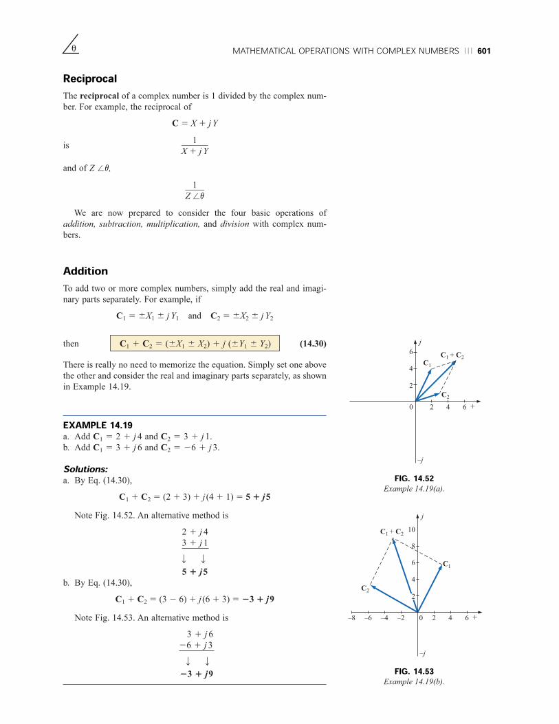
–j
j
+
C1
C1 + C2
C2
6
4
0 2 4 6–2–4–6–8
8
10
2
–j
j
+
C1
C1 + C2
C2
6
4
2
0 2 4 6
u
ReciprocalThe reciprocal of a complex number is 1 divided by the complex num-
ber. For example, the reciprocal of
C 5 X 1 j Y
is
and of Z /v,
We are now prepared to consider the four basic operations of
addition, subtraction, multiplication, and division with complex num-
bers.
AdditionTo add two or more complex numbers, simply add the real and imagi-
nary parts separately. For example, if
C1 5 6X1 6 j Y1 and C2 5 6X2 6 j Y2
then (14.30)
There is really no need to memorize the equation. Simply set one above
the other and consider the real and imaginary parts separately, as shown
in Example 14.19.
EXAMPLE 14.19a. Add C1 5 2 1 j 4 and C2 5 3 1 j 1.
b. Add C1 5 3 1 j 6 and C2 5 26 1 j 3.
Solutions:a. By Eq. (14.30),
C1 1 C2 5 (2 1 3) 1 j(4 1 1) 5 5 1 j5
Note Fig. 14.52. An alternative method is
2 1 j 4
3 1 j 1
C1 1 C2 5 (6X1 6 X2) 1 j (6Y1 6 Y2)
1Z /v
1X 1 j Y
MATHEMATICAL OPERATIONS WITH COMPLEX NUMBERS 601
FIG. 14.52Example 14.19(a).
FIG. 14.53Example 14.19(b).
5 1 j5
b. By Eq. (14.30),
C1 1 C2 5 (3 2 6) 1 j(6 1 3) 5 23 1 j9
Note Fig. 14.53. An alternative method is
3 1 j 6
26 1 j 3
23 1 j9
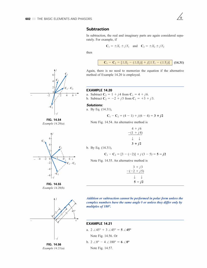
2
+–
–j
j
3 5
45°
–j
j
+
C1
C1 – C2
C2
6
4
2
0 2 4 6–2–
–2
–4
–6
–4
–C2
–j
j
+
C1
C1 – C2
C2
6
4
2
0
2 4 6–2–
–C2
602 THE BASIC ELEMENTS AND PHASORS
SubtractionIn subtraction, the real and imaginary parts are again considered sepa-
rately. For example, if
C1 5 6X1 6 j Y1 and C2 5 6X2 6 j Y2
then
(14.31)
Again, there is no need to memorize the equation if the alternative
method of Example 14.20 is employed.
EXAMPLE 14.20a. Subtract C2 5 1 1 j 4 from C1 5 4 1 j 6.
b. Subtract C2 5 22 1 j 5 from C1 5 13 1 j 3.
Solutions:a. By Eq. (14.31),
C1 2 C2 5 (4 2 1) 1 j (6 2 4) 5 3 1 j2
Note Fig. 14.54. An alternative method is
4 1 j 6
2(1 1 j 4)
3 1 j2
b. By Eq. (14.31),
C1 2 C2 5 [3 2 (22)] 1 j (3 2 5) 5 5 2 j2
Note Fig. 14.55. An alternative method is
3 1 j 3
2(22 1 j 5)
5 2 j2
Addition or subtraction cannot be performed in polar form unless the
complex numbers have the same angle v or unless they differ only by
multiples of 180°.
EXAMPLE 14.21a. 2 /45° 1 3 /45° 5 5 /45°
Note Fig. 14.56. Or
b. 2 /0° 2 4 /180° 5 6 /0°
Note Fig. 14.57.
C1 2 C2 5 [6X2 2 (6X2)] 1 j[6Y1 2 (6Y2)]
u
FIG. 14.54Example 14.20(a).
FIG. 14.55Example 14.20(b).
FIG. 14.56Example 14.21(a).

u
MultiplicationTo multiply two complex numbers in rectangular form, multiply the
real and imaginary parts of one in turn by the real and imaginary parts
of the other. For example, if
C1 5 X1 1 j Y1 and C2 5 X2 1 j Y2
then C1 ⋅ C2: X1 1 j Y1
and (14.32)
In Example 14.22(b), we obtain a solution without resorting to mem-
orizing Eq. (14.32). Simply carry along the j factor when multiplying
each part of one vector with the real and imaginary parts of the other.
EXAMPLE 14.22a. Find C1 ⋅ C2 if
C1 5 2 1 j 3 and C2 5 5 1 j 10
b. Find C1 ⋅ C2 if
C1 5 22 2 j 3 and C2 5 14 2 j 6
Solutions:a. Using the format above, we have
C1 ⋅ C25 [(2)(5) 2 (3)(10)] 1 j [(3)(5) 1 (2)(10)]
5 220 1 j35
b. Without using the format, we obtain
22 2 j 3
14 2 j 6
28 2 j 12
1 j 12 1 j 218
28 1 j (212 1 12) 2 18
and C1 ⋅ C2 5 226 5 26 /180°
C1 ⋅ C2 5 (X1X2 2 Y1Y2) 1 j (Y1X2 1 X1Y2)
1 j X1Y2 1 j 2Y1Y2X1X2 1 j (X1Y1X2 1 X1Y2) 1 Y1Y2(21)
X2 1 j Y2X1X2 1 j Y1X2
MATHEMATICAL OPERATIONS WITH COMPLEX NUMBERS 603
FIG. 14.57Example 14.21(b).
+–
–j
j
6
2
–4 / 180°
4 / 180°

604 THE BASIC ELEMENTS AND PHASORS
In polar form, the magnitudes are multiplied and the angles added
algebraically. For example, for
C1 5 Z1 /v1 and C2 5 Z2 /v2
we write
(14.33)
EXAMPLE 14.23a. Find C1 ⋅ C2 if
C1 5 5 /20° and C2 5 10 /30°
b. Find C1 ⋅ C2 if
C1 5 2 /240° and C2 5 7 /1120°
Solutions:a. C1 ⋅ C2 5 (5 /20°)(10 /30°) 5 (5)(10) /20° 1 30° 5 50 /50°
b. C1 ⋅ C2 5 (2 /240°)(7 /1120°) 5 (2)(7) /240° 1 120°
5 14 /180°
To multiply a complex number in rectangular form by a real number
requires that both the real part and the imaginary part be multiplied by
the real number. For example,
(10)(2 1 j 3) 5 20 1 j 30
and 50 /0°(0 1 j 6) 5 j 300 5 300 /90°
DivisionTo divide two complex numbers in rectangular form, multiply the
numerator and denominator by the conjugate of the denominator and
the resulting real and imaginary parts collected. That is, if
C1 5 X1 1 jY1 and C2 5 X2 1 jY2
then 5
5
and 5 1 j (14.34)
The equation does not have to be memorized if the steps above used
to obtain it are employed. That is, first multiply the numerator by the
complex conjugate of the denominator and separate the real and imagi-
nary terms. Then divide each term by the sum of each term of the
denominator squared.
EXAMPLE 14.24a. Find C1/C2 if C1 5 1 1 j 4 and C2 5 4 1 j 5.
b. Find C1/C2 if C1 5 24 2 j 8 and C2 5 16 2 j 1.
X2Y1 2 X1Y2
X22 1 Y2
2
X1X2 1 Y1Y2
X22 1 Y2
2
C1C2
(X1X2 1 Y1Y2) 1 j(X2Y1 2 X1Y2)
X22 1 Y2
2
(X1 1 jY1)(X2 2 jY2)(X2 1 jY2)(X2 2 jY2)
C1C2
C1 ⋅ C2 5 Z1Z2 / v1 1 v2
u

u
Solutions:a. By Eq. (14.34),
5 1 j
5 1 > 0.585 1 j 0.268
b. Using an alternative method, we obtain
24 2 j 8
16 1 j 1
224 2 j 48
2 j 4 2 j28
224 2 j 52 1 8 5 216 2 j 52
16 2 j 1
16 1 j 1
36 1 j 6
2 j 6 2 j21
36 10 1 1 5 37
and 5 2 5 20.432 2j1.405
To divide a complex number in rectangular form by a real number,
both the real part and the imaginary part must be divided by the real
number. For example,
5 4 1 j 5
and 5 3.4 2j 0 5 3.4 /0°
In polar form, division is accomplished by simply dividing the mag-
nitude of the numerator by the magnitude of the denominator and sub-
tracting the angle of the denominator from that of the numerator. That
is, for
C1 5 Z1 /v1 and C2 5 Z2 /v2
we write
5 /v1 2 v2 (14.35)
EXAMPLE 14.25a. Find C1/C2 if C1 5 15 /10° and C2 5 2 /7°.
b. Find C1/C2 if C1 5 8 /120° and C2 5 16 /250°.
Solutions:a. 5 5 /10° 2 7° 5 7.5 /3°
152
15 /10°2 /7°
C1C2
Z1Z2
C1C2
6.8 2 j 0
2
8 1 j 10
2
j5237
216
37
C1C2
j 1141
2441
(4)(4) 2 (1)(5)
421 52
(1)(4) 1 (4)(5)
421 52
C1C2
MATHEMATICAL OPERATIONS WITH COMPLEX NUMBERS 605

606 THE BASIC ELEMENTS AND PHASORS
b. 5 5 /120° 2 (250°) 5 0.5 /170°
We obtain the reciprocal in the rectangular form by multiplying the
numerator and denominator by the complex conjugate of the denomi-
nator:
5 1 21 2 5
and 5 2 j (14.36)
In polar form, the reciprocal is
5 /2v (14.37)
A concluding example using the four basic operations follows.
EXAMPLE 14.26 Perform the following operations, leaving the answer
in polar or rectangular form:
a. 5
5
5
5 5 0.983 2 j0.207
b. 5 5
5 35.35 /75° 2 (220°) 5 35.35 /95°
c. 5
5 5
5 2 /93.13° 2 (236.87°) 5 2.0 /130°
d. 3 /27° 2 6 /240° 5 (2.673 1 j 1.362) 2 (4.596 2 j 3.857)
5 (2.673 2 4.596) 1 j (1.362 1 3.857)
5 21.923 1 j 5.219
14.11 CALCULATOR AND COMPUTERMETHODS WITH COMPLEX NUMBERSThe process of converting from one form to another or working through
lengthy operations with complex numbers can be time-consuming and
20 /93.13°10 /236.87°
(4 /40°)(5 /53.13°)
10 /236.87°
(2 /20°)(2 /20°)(5 /53.13°)
10 /236.87°
(2 /20°)2(3 1 j 4)
8 2 j 6
353.5 /75°10 /220°
(50 /30°)(7.07 /45°)
10 /220°
(50 /30°)(5 1 j 5)
10 /220°
114 2 j 24
116
[(6)(4) 1 (9)(10)] 1 j [(4)(9) 2 (6)(10)]
421 102
(6 1 j 9)(4 2 j 10)(4 1 j 10)(4 2 j 10)
(2 1 4) 1 j (3 1 6)(7 2 3) 1 j (7 1 3)
(2 1 j 3) 1 (4 1 j 6)(7 1 j 7) 2 (3 2 j 3)
1Z
1Z /v
YX2
1 Y2
XX2
1 Y2
1X 1 j Y
X 2 j YX2
1 Y2
X 2 j YX 2 j Y
1X 1 j Y
1X 1 j Y
816
8 /120°16 /250°
C1C2
u

u
often frustrating if one lost minus sign or decimal point invalidates the
solution. Fortunately, technologists of today have calculators and com-
puter methods that make the process measurably easier with higher
degrees of reliability and accuracy.
CalculatorsThe TI-86 calculator of Fig. 14.58 is only one of numerous calculators
that can convert from one form to another and perform lengthy calcula-
tions with complex numbers in a concise, neat form. Not all of the
details of using a specific calculator will be included here because each
has its own format and sequence of steps. However, the basic operations
with the TI-86 will be included primarily to demonstrate the ease with
which the conversions can be made and the format for more complex
operations.
For the TI-86 calculator, one must first call up the 2nd function
CPLX from the keyboard, which results in a menu at the bottom of the
display including conj, real, imag, abs, and angle. If we choose the key
MORE, c Rec and c Pol will appear as options (for the conversion
process). To convert from one form to another, simply enter the current
form in brackets with a comma between components for the rectangu-
lar form and an angle symbol for the polar form. Follow this form with
the operation to be performed, and press the ENTER key—the result
will appear on the screen in the desired format.
EXAMPLE 14.27 This example is for demonstration purposes only. It
is not expected that all readers will have a TI-86 calculator. The sole
purpose of the example is to demonstrate the power of today’s calcula-
tors.
Using the TI-86 calculator, perform the following conversions:
a. 3 2 j 4 to polar form.
b. 0.006 /20.6° to rectangular form.
Solutions:a. The TI-86 display for part (a) is the following:
CALCULATOR AND COMPUTER METHODS WITH COMPLEX NUMBERS 607
CALC. 14.1
(0.006/20.6) c Rec ENTER(5.616E23, 2.111E23)
CALC. 14.2
FIG. 14.58TI-86 scientific calculator. (Courtesy of Texas
Instruments, Inc.)
(3, 24) c Pol ENTER(5.000E0/253.130E0)
b. The TI-86 display for part (b) is the following:
EXAMPLE 14.28 Using the TI-86 calculator, perform the desired
operations required in part (c) of Example 14.26, and compare solutions.
Solution: One must now be aware of the hierarchy of mathematical
operations. In other words, in which sequence will the calculator per-
form the desired operations? In most cases, the sequence is the same as

608 THE BASIC ELEMENTS AND PHASORS
that used in longhand calculations, although one must become adept at
setting up the parentheses to ensure the correct order of operations. For
this example, the TI-86 display is the following:
u
((2/20)2*(3,4))/(8,26)c Pol ENTER(2.000E0/130.000E0)
CALC. 14.3
MathcadThe Mathcad format for complex numbers will now be introduced in
preparation for the chapters to follow. We will continue to use j when
we define a complex number in rectangular form even though the Math-
cad result will always appear with the letter i. You can change this by
going to the Format menu, but for this presentation we decided to use
the default operators as much as possible.
When entering j to define the imaginary component of a complex
number, be sure to enter it as 1j; but do not put a multiplication opera-
tor between the 1 and the j. Just type 1 and then j. In addition, place the
j after the constant rather than before as in the text material.
When Mathcad operates on an angle, it will assume that the angle is
in radians and not degrees. Further, all results will appear in radians
rather than degrees.
The first operation to be developed is the conversion from rectangu-
lar to polar form. In Fig. 14.59 the rectangular number 4 1 j 3 is being
converted to polar form using Mathcad. First X and Y are defined using
the colon operator. Next the equation for the magnitude of the polar
form is written in terms of the two variables just defined. The magni-
tude of the polar form is then revealed by writing the variable again and
using the equal sign. It will take some practice, but be careful when
writing the equation for Z in the sense that you pay particular attention
to the location of the bracket before performing the next operation. The
resulting magnitude of 5 is as expected.
For the angle, the sequence View-Toolbars-Greek is first applied to
obtain the Greek toolbar appearing in Fig. 14.59. It can be moved to
any location by simply clicking on the blue at the top of the toolbar and
dragging it to the preferred location. Then 0 is selected from the toolbar
as the variable to be defined. The tan21 v is obtained through the
sequence Insert-f(x)-Insert Function dialog box-trigonometric-atan-
OK in which Y/X is inserted. Then bring the controlling bracket to the
outside of the entire expression, and multiply by the ratio of 180/p with
p selected from the Calculator toolbar (available from the same
sequence used to obtain the Greek toolbar). The multiplication by the
last factor of the equation will ensure that the angle is in degrees.
Selecting v again followed by an equal sign will result in the correct
angle of 36.87° as shown in Fig. 14.59.
We will now look at two forms for the polar form of a complex num-
ber. The first is defined by the basic equations introduced in this chap-
ter, while the second uses a special format. For all the Mathcad analy-
ses to be provided in this text, the latter format will be employed. First
which is a perfect match with the earlier solution.
German-American(Breslau, Germany;Yonkers and Schenectady,NY, USA)
(1865–1923)Mathematician,
Scientist,Engineer, Inventor,Professor of Electrical Engineering and Electrophysics,Union College
Department Head,General Electric Co.
Although the holder of some 200 patents and recog-
nized worldwide for his contributions to the study of
hysteresis losses and electrical transients, Charles
Proteus Steinmetz is best recognized for his contri-
bution to the study of ac networks. His “Symbolic
Method of Alternating-current Calculations” pro-
vided an approach to the analysis of ac networks
that removed a great deal of the confusion and frus-
tration experienced by engineers of that day as they
made the transition from dc to ac systems. His
approach (from which the phasor notation of this
text is premised) permitted a direct analysis of ac
systems using many of the theorems and methods of
analysis developed for dc systems. In 1897 he
authored the epic work Theory and Calculation of
Alternating Current Phenomena, which became the
“bible” for practicing engineers. Dr. Steinmetz was
fondly referred to as “The Doctor” at General Elec-
tric Company where he worked for some 30 years in
a number of important capacities. His recognition as
a “multigifted genius” is supported by the fact that
he maintained active friendships with such individu-
als as Albert Einstein, Guglielmo Marconi (radio),
and Thomas A. Edison, to name just a few. He was
President of the American Institute of Electrical
Engineers (AIEE) and the National Association of
Corporation Schools and actively supported his
local community (Schenectady) as president of the
Board of Education and the Commission on Parks
and City Planning.
CHARLES PROTEUS STEINMETZ
Courtesy of the
Hall of History Foundation,
Schenectady, New York

u
the magnitude of the polar form is defined followed by the conversion
of the angle of 60° to radians by multiplying by the factor p/180 as
shown in Fig. 14.60. In this example the resulting angular measure is
p/3 radians. Next the rectangular format is defined by a real part X 5
Z cos v and by an imaginary part Y 5 Z sin v. Both the cos and the sin
are obtained by the sequence Insert-f(x)-trigonometric-cos(or sin)-
OK. Note the multiplication by j which was actually entered as 1j.
Entering C again followed by an equal sign will result in the correct
conversion shown in Fig. 14.60.
The next format is based on the mathematical relationship that e jv5
cos v 1 j sin v. Both Z and v are as defined above, but now the complex
number is written as shown in Fig. 14.60 using the notation just intro-
duced. Note that both Z and v are part of this defining form. The ex is
obtained directly from the Calculator toolbar. Remember to enter the j
as 1j without a multiplication sign between the 1 and the j. However,
there is a multiplication operator placed between the j and v. When
entered again followed by an equal sign, the rectangular form appears
to match the above results. As mentioned above, it is this latter format
that will be used throughout the text due to its cleaner form and more
direct entering path.
The last example using Mathcad will be a confirmation of the results
of Example 14.26(b) as shown in Fig. 14.61. The three complex num-
bers are first defined as shown. Then the equation for the desired result
CALCULATOR AND COMPUTER METHODS WITH COMPLEX NUMBERS 609
FIG. 14.59Using Mathcad to convert from rectangular to polar form.
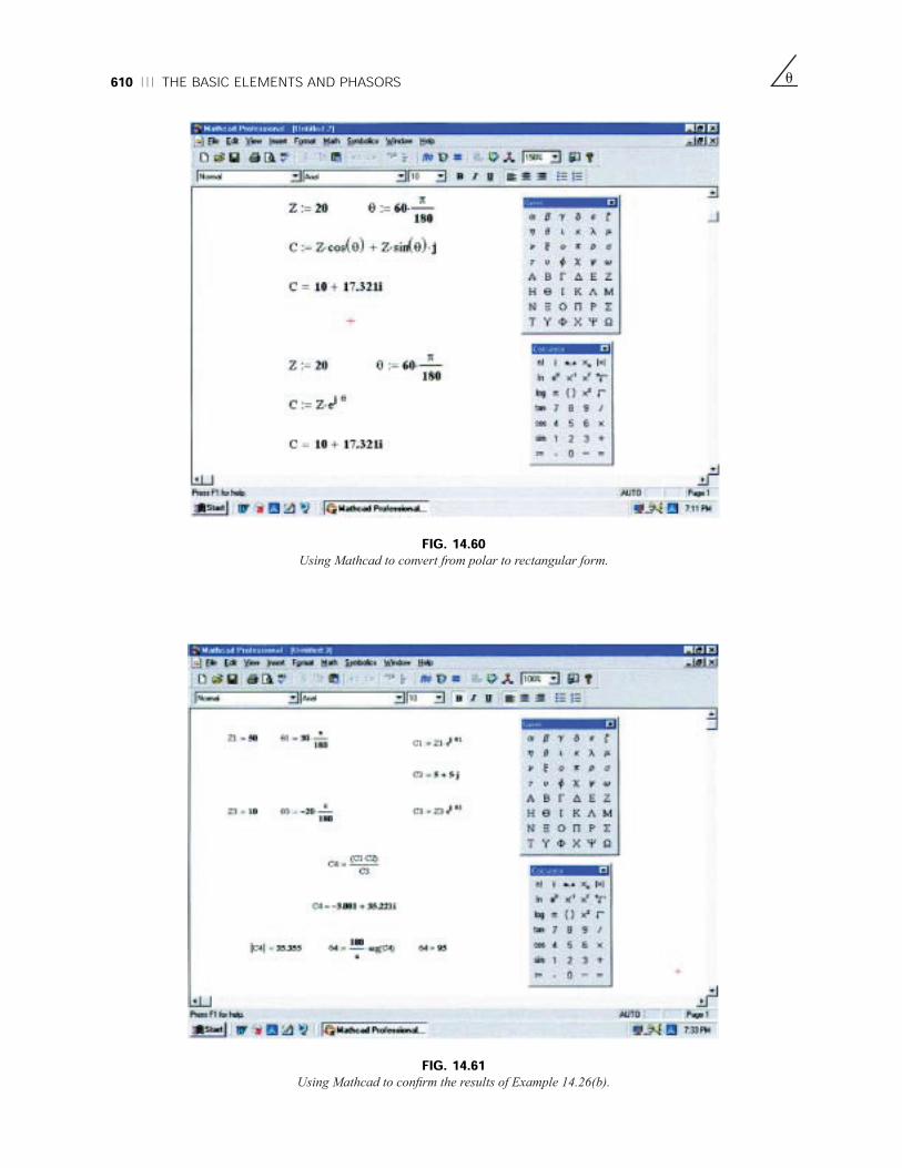
610 THE BASIC ELEMENTS AND PHASORS u
FIG. 14.60Using Mathcad to convert from polar to rectangular form.
FIG. 14.61Using Mathcad to confirm the results of Example 14.26(b).

u PHASORS 611
is entered using C4, and finally the results are called for. Note the rela-
tive simplicity of the equation for C4 now that all the other variables
have been defined. As shown, however, the immediate result is in the
rectangular form using the magnitude feature from the calculator and
the arg function from Insert-f(x)-Complex Numbers-arg. There will
be a number of other examples in the chapters to follow on the use of
Mathcad with complex numbers.
14.12 PHASORSAs noted earlier in this chapter, the addition of sinusoidal voltages
and currents will frequently be required in the analysis of ac circuits.
One lengthy but valid method of performing this operation is to place
both sinusoidal waveforms on the same set of axes and add alge-
braically the magnitudes of each at every point along the abscissa, as
shown for c 5 a 1 b in Fig. 14.62. This, however, can be a long and
tedious process with limited accuracy. A shorter method uses the
rotating radius vector first appearing in Fig. 13.16. This radius vector,
having a constant magnitude (length) with one end fixed at the ori-
gin, is called a phasor when applied to electric circuits. During its
rotational development of the sine wave, the phasor will, at the
instant t 5 0, have the positions shown in Fig. 14.63(a) for each
waveform in Fig. 14.63(b).
v1a
b
0 t
v2
vT = v1 + v2c = a + b
v
FIG. 14.62Adding two sinusoidal waveforms on a point-by-point basis.
Note in Fig. 14.63(b) that v2 passes through the horizontal axis at
t 5 0 s, requiring that the radius vector in Fig. 14.63(a) be on the hori-
zontal axis to ensure a vertical projection of zero volts at t 5 0 s. Its
length in Fig. 14.63(a) is equal to the peak value of the sinusoid as
required by the radius vector of Fig. 13.16. The other sinusoid has
passed through 90° of its rotation by the time t 5 0 s is reached and
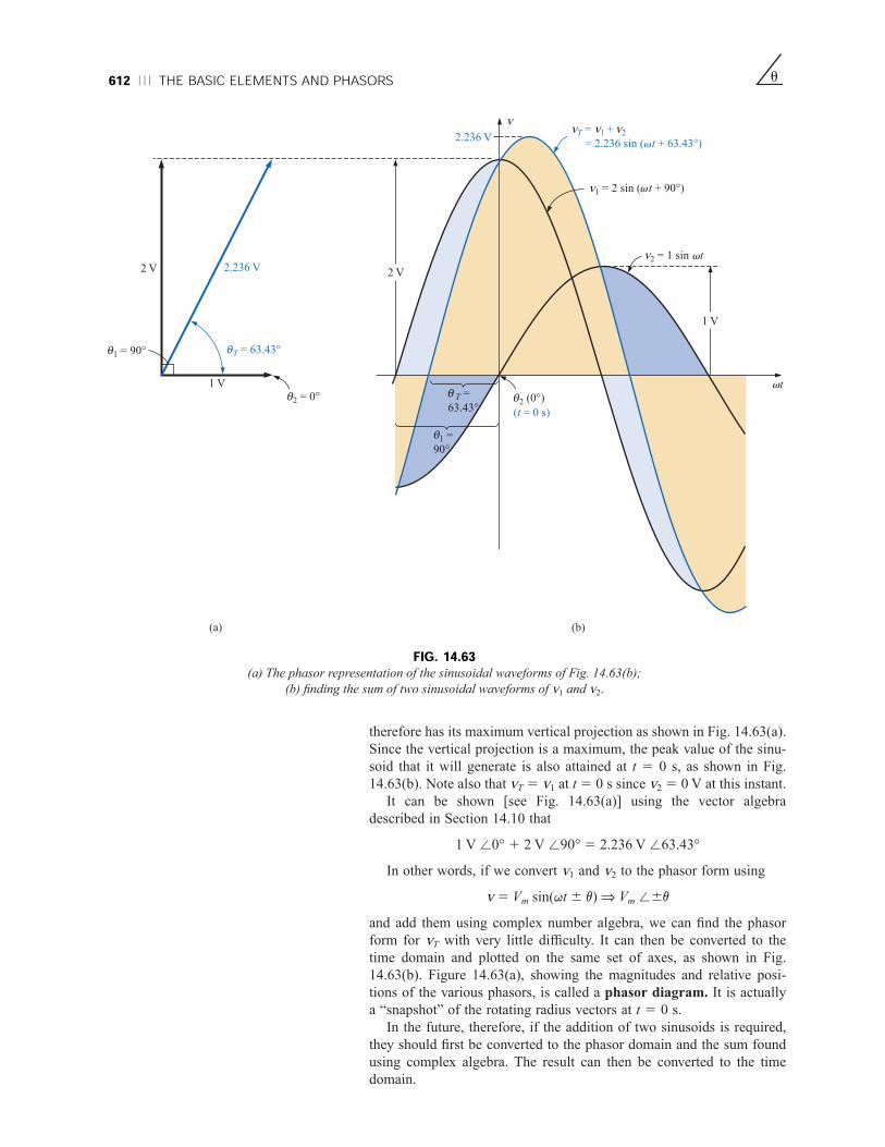
612 THE BASIC ELEMENTS AND PHASORS
therefore has its maximum vertical projection as shown in Fig. 14.63(a).
Since the vertical projection is a maximum, the peak value of the sinu-
soid that it will generate is also attained at t 5 0 s, as shown in Fig.
14.63(b). Note also that vT 5 v1 at t 5 0 s since v2 5 0 V at this instant.
It can be shown [see Fig. 14.63(a)] using the vector algebra
described in Section 14.10 that
1 V /0° 1 2 V /90° 5 2.236 V /63.43°
In other words, if we convert v1 and v2 to the phasor form using
v 5 Vm sin(qt 6 v) ⇒ Vm /6v
and add them using complex number algebra, we can find the phasor
form for vT with very little difficulty. It can then be converted to the
time domain and plotted on the same set of axes, as shown in Fig.
14.63(b). Figure 14.63(a), showing the magnitudes and relative posi-
tions of the various phasors, is called a phasor diagram. It is actually
a “snapshot” of the rotating radius vectors at t 5 0 s.
In the future, therefore, if the addition of two sinusoids is required,
they should first be converted to the phasor domain and the sum found
using complex algebra. The result can then be converted to the time
domain.
u
1 V
2 V
v2.236 V
1 V
2.236 V2 V
(a) (b)
v1 = 2 sin ( t + 90°)v
vT = v1 + v2
= 2.236 sin ( t + 63.43°)v
v2 = 1 sin tv
tv
2 (0°)
(t = 0 s)
θ
1 =
90°θ
T =
63.43°θ 2 = 0°θ
T = 63.43°θ 1 = 90°θ
FIG. 14.63(a) The phasor representation of the sinusoidal waveforms of Fig. 14.63(b);
(b) finding the sum of two sinusoidal waveforms of v1 and v2.

u PHASORS 613
The case of two sinusoidal functions having phase angles different
from 0° and 90° appears in Fig. 14.64. Note again that the vertical
height of the functions in Fig. 14.64(b) at t 5 0 s is determined by the
rotational positions of the radius vectors in Fig. 14.64(a).
Since the rms, rather than the peak, values are used almost exclu-
sively in the analysis of ac circuits, the phasor will now be redefined for
the purposes of practicality and uniformity as having a magnitude equal
to the rms value of the sine wave it represents. The angle associated
with the phasor will remain as previously described—the phase angle.
In general, for all of the analyses to follow, the phasor form of a
sinusoidal voltage or current will be
V 5 V /v and I 5 I /v
where V and I are rms values and v is the phase angle. It should be
pointed out that in phasor notation, the sine wave is always the refer-
ence, and the frequency is not represented.
Phasor algebra for sinusoidal quantities is applicable only for
waveforms having the same frequency.
EXAMPLE 14.29 Convert the following from the time to the phasor
domain:
6 A 5 A
ImT
0°(t = 0 s)
i
5 A
6 A
10.63 A
(a) (b)
iT = i1 + i2 = 10.63 sin(qt + 46.40°)
i1 = 5 sin(qt + 30°)
qt
i2 = 6 sin(qt + 60°)
v1 = 30°
vT
v2 = 60°
v2 = 60°
v1 = 30°
vT = 46.40°
FIG. 14.64Adding two sinusoidal currents with phase angles other than 90°.
Time Domain Phasor Domain
a. Ï2w(50) sin qt 50 /0°
b. 69.6 sin(qt 1 72°) (0.707)(69.6) /72° 5 49.21 /72°
c. 45 cos qt (0.707)(45) /90° 5 31.82 /90°

EXAMPLE 14.31 Find the input voltage of the circuit of Fig. 14.65 if
va 5 50 sin(377t 1 30°)
vb 5 30 sin(377t 1 60°)f 5 60 Hz
Phasor Domain Time Domain
a. I 5 10 /30° i 5 Ï2w(10) sin(2p60t 1 30°)
and i 5 14.14 sin(377t 1 30°)
b. V 5 115 /270° v 5 Ï2w(115) sin(377t 2 70°)
and v 5 162.6 sin(377t 2 70°)
EXAMPLE 14.30 Write the sinusoidal expression for the following
phasors if the frequency is 60 Hz:
+
–
+
–
+ –
ein
va
vb
FIG. 14.65Example 14.31.
614 THE BASIC ELEMENTS AND PHASORS u
Solution: Applying Kirchhoff’s voltage law, we have
ein 5 va 1 vb
Converting from the time to the phasor domain yields
va 5 50 sin(377t 1 30°) ⇒ Va 5 35.35 V /30°
vb 5 30 sin(377t 1 60°) ⇒ Vb 5 21.21 V /60°
Converting from polar to rectangular form for addition yields
Va 5 35.35 V /30° 5 30.61 V 1 j 17.68 V
Vb 5 21.21 V /60° 5 10.61 V 1 j 18.37 V
Then
Ein 5 Va 1 Vb 5 (30.61 V 1 j 17.68 V) 1 (10.61 V 1 j 18.37 V)
5 41.22 V 1 j 36.05 V
Converting from rectangular to polar form, we have
Ein 5 41.22 V 1 j 36.05 V 5 54.76 V /41.17°
Converting from the phasor to the time domain, we obtain
Ein 5 54.76 V /41.17° ⇒ ein 5 Ï2w(54.76) sin(377t 1 41.17°)
and ein 5 77.43 sin(377t 1 41.17°)
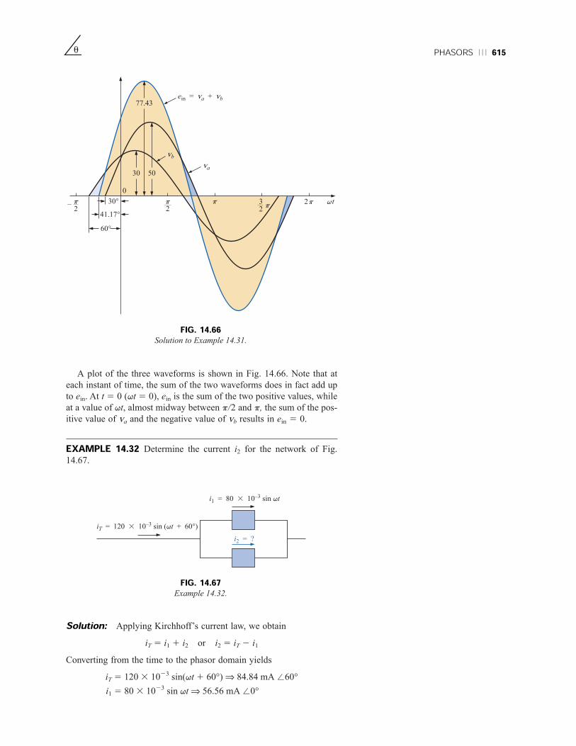
u PHASORS 615
A plot of the three waveforms is shown in Fig. 14.66. Note that at
each instant of time, the sum of the two waveforms does in fact add up
to ein. At t 5 0 (qt 5 0), ein is the sum of the two positive values, while
at a value of qt, almost midway between p/2 and p, the sum of the pos-
itive value of va and the negative value of vb results in ein 5 0.
EXAMPLE 14.32 Determine the current i2 for the network of Fig.
14.67.
ein = va + vb
60°
41.17°
30°
30 50
77.43
va
vb
0
–2p
2p p 3
2p
2p tq
FIG. 14.66Solution to Example 14.31.
iT = 120 3 10–3 sin (qt + 60°)
i1 = 80 3 10–3 sin qt
i2 = ?
FIG. 14.67Example 14.32.
Solution: Applying Kirchhoff’s current law, we obtain
iT 5 i1 1 i2 or i2 5 iT 2 i1
Converting from the time to the phasor domain yields
iT 5 120 3 1023 sin(qt 1 60°) ⇒ 84.84 mA /60°
i1 5 80 3 1023 sin qt ⇒ 56.56 mA /0°

616 THE BASIC ELEMENTS AND PHASORS u
Converting from polar to rectangular form for subtraction yields
IT 5 84.84 mA /60° 5 42.42 mA 1 j 73.47 mA
I1 5 56.56 mA /0° 5 56.56 mA 1 j 0
Then
I2 5 IT 2 I1
5 (42.42 mA 1 j 73.47 mA) 2 (56.56 mA 1 j 0)
and I2 5 214.14 mA 1 j 73.47 mA
Converting from rectangular to polar form, we have
I2 5 74.82 mA /100.89°
Converting from the phasor to the time domain, we have
I2 5 74.82 mA /100.89° ⇒i2 5 Ï2w(74.82 3 1023) sin(qt 1 100.89°)
and i2 5 105.8 3 1023
sin(qt 1 100.89°)
A plot of the three waveforms appears in Fig. 14.68. The waveforms
clearly indicate that iT 5 i1 1 i2.
i2
60°100.89°
0°
80105.8
120i1
iT
i (mA)
i2 = iT – i1
p–2p
2p 3
2p
2p
FIG. 14.68Solution to Example 14.32.
14.13 COMPUTER ANALYSISPSpiceCapacitors and the ac Response The simplest of ac capacitive
circuits will now be analyzed to introduce the process of setting up an
ac source and running an ac transient simulation. The ac source of Fig.

u COMPUTER ANALYSIS 617
14.69 is obtained through Place part key-SOURCE-VSIN-OK. The
name or value of any parameter can be changed by simply double-
clicking on the parameter on the display or by double-clicking on the
source symbol to get the Property Editor dialog box. Within the dia-
log box the values appearing in Fig. 14.69 were set, and under Display,
Name and Value were selected. After you have selected Apply and
exited the dialog box, the parameters will appear as shown in the figure.
The simulation process is initiated by selecting the New Simulation
Profile and under New Simulation entering Transientac for the Name
followed by Create. In the Simulation Settings dialog box, Analysis is
selected and Time Domain(Transient) is chosen under Analysis type.
The Run to time will be set at 3 ms to permit a display of three cycles of
the sinusoidal waveforms (T 5 1/f 5 1/1000 Hz 5 1 ms). The Start
saving data after will be left at 0 s, and the Maximum step size will be
3 ms/1000 5 3 ms. Clicking OK and then selecting the Run PSpice icon
will result in a plot having a horizontal axis that extends from 0 to 3 ms.
Now we have to tell the computer which waveforms we are inter-
ested in. First, we should take a look at the applied ac source by select-
ing Trace-Add Trace-V(Vs:1) followed by OK. The result is the
sweeping ac voltage in the botttom region of the screen of Fig. 14.70.
Note that it has a peak value of 5 V, and three cycles appear in the 3-ms
time frame. The current for the capacitor can be added by selecting
Trace-Add Trace and choosing I(C) followed by OK. The resulting
waveform for I(C) appears at a 90° phase shift from the applied volt-
age, with the current leading the voltage (the current has already peaked
FIG. 14.69Using PSpice to analyze the response of a capacitor to a sinusoidal ac signal.
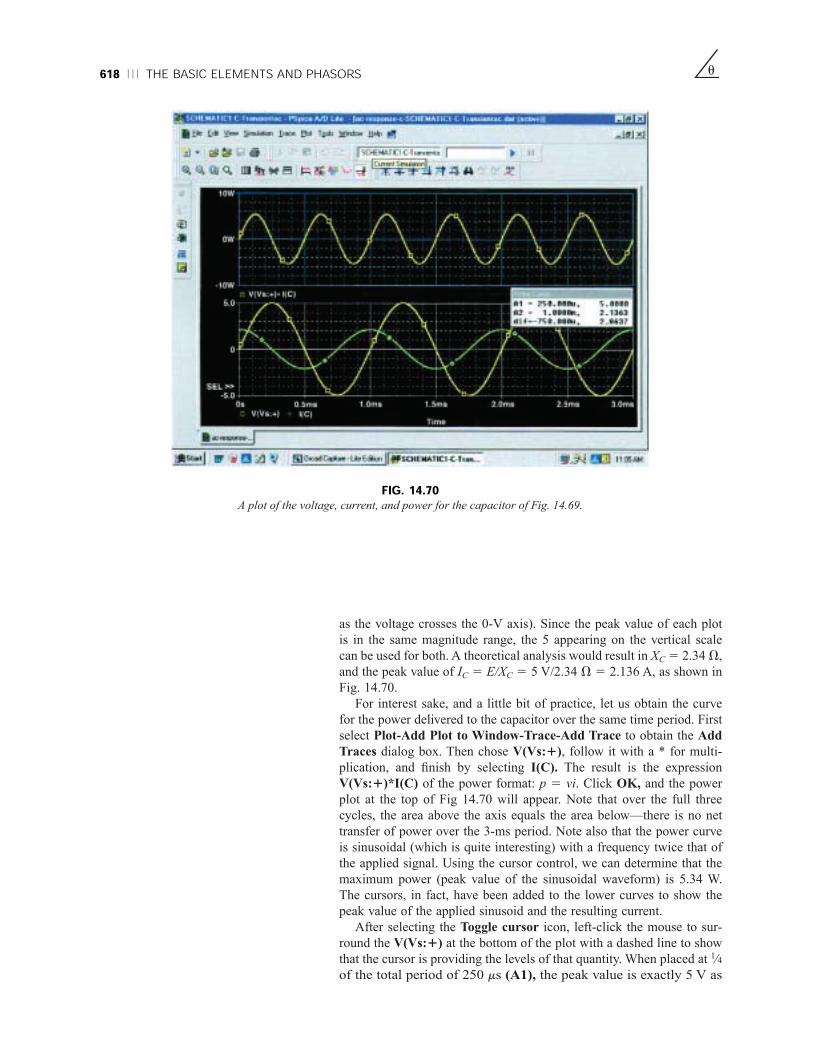
as the voltage crosses the 0-V axis). Since the peak value of each plot
is in the same magnitude range, the 5 appearing on the vertical scale
can be used for both. A theoretical analysis would result in XC 5 2.34 V,
and the peak value of IC 5 E/XC 5 5 V/2.34 V 5 2.136 A, as shown in
Fig. 14.70.
For interest sake, and a little bit of practice, let us obtain the curve
for the power delivered to the capacitor over the same time period. First
select Plot-Add Plot to Window-Trace-Add Trace to obtain the Add
Traces dialog box. Then chose V(Vs:1), follow it with a * for multi-
plication, and finish by selecting I(C). The result is the expression
V(Vs:1)*I(C) of the power format: p 5 vi. Click OK, and the power
plot at the top of Fig 14.70 will appear. Note that over the full three
cycles, the area above the axis equals the area below—there is no net
transfer of power over the 3-ms period. Note also that the power curve
is sinusoidal (which is quite interesting) with a frequency twice that of
the applied signal. Using the cursor control, we can determine that the
maximum power (peak value of the sinusoidal waveform) is 5.34 W.
The cursors, in fact, have been added to the lower curves to show the
peak value of the applied sinusoid and the resulting current.
After selecting the Toggle cursor icon, left-click the mouse to sur-
round the V(Vs:1) at the bottom of the plot with a dashed line to show
that the cursor is providing the levels of that quantity. When placed at 1⁄4
of the total period of 250 ms (A1), the peak value is exactly 5 V as
618 THE BASIC ELEMENTS AND PHASORS u
FIG. 14.70A plot of the voltage, current, and power for the capacitor of Fig. 14.69.

u COMPUTER ANALYSIS 619
FIG. 14.71Using Electronics Workbench to review the response of an inductive element
to a sinusoidal ac signal.
shown in the Probe Cursor dialog box. Placing the cursor over the
symbol next to I(C) at the bottom of the plot and right-clicking the
mouse will assign the right cursor to the current. Placing it at exactly
1 ms (A2) will result in a peak value of 2.136 A to match the solution
above. To further distinguish between the voltage and current wave-
forms, the color and the width of the lines of the traces were changed.
Place the cursor right on the plot line and perform a right click. Then
the Properties option appears. When Properties is selected, a Trace
Properties dialog box will appear in which the yellow color can be
selected and the width widened to improve the visibility on the black
background. Note that yellow was chosen for Vs and green for I(C).
Note also that the axis and the grid have been changed to a more visi-
ble color using the same procedure.
Electronics WorkbenchSince PSpice reviewed the response of a capacitive element to an ac
voltage, Electronics Workbench will repeat the analysis for an inductive
element. The ac voltage source was derived from the Sources parts bin
as described in Chapter 13 with the values appearing in Fig. 14.71 set in
the AC Voltage dialog box. Since the transient response of Electronics
Workbench is limited to a plot of voltage versus time, a plot of the cur-
rent of the circuit will require the addition of a resistor of 1 V in series

620 THE BASIC ELEMENTS AND PHASORS
with the inductive element. The magnitude of the current through the
resistor and, of course, the series inductor will then be determined by
| iR | 5 | | 5 | | 5 | vR | 5 | iL |
revealing that the current will have the same peak value as the voltage
across the resistor due to the division by 1. When viewed on the graph,
it can simply be considered a plot of the current. In actuality, all
inductors require a series resistance, so the 1-V resistor serves an
important dual purpose. The 1-V resistance is also so small compared
to the reactance of the coil at the 1-kHz frequency that its effect on the
total impedance or voltage across the coil can be ignored.
Once the circuit has been constructed, the sequence Simulate-
Analyses-Transient Analysis will result in a Transient Analysis dia-
log box in which the Start time is set at 0 s and the End time at 105 ms.
The 105 ms was set as the End time to give the network 100 ms to set-
tle down in its steady-state mode and 5 ms for five cycles in the output
display. The Minimum number of time points was set at 10,000 to
ensure a good display for the rapidly changing waveforms.
Next the Output variables heading was chosen within the dialog
box, and nodes 1 and 2 were moved from the Variables in Circuit to
Selected variables for analysis using the Plot during simulation key
pad. Choosing Simulate will then result in a waveform that extends
from 0 s to 105 ms. Even though we plan to save only the response that
occurs after 100 ms, the computer is unaware of our interest, and it
plots the response for the entire period, This is corrected by selecting
the Properties key pad in the toolbar at the top of the graph (it looks
like a tag and pencil) to obtain the Graph Properties dialog box.
Selecting Bottom Axis will permit setting the Range from a Minimum
of 0.100s5100ms to a Maximum of 0.105s5105ms. Click OK, and
the time period of Fig. 14.71 will be displayed. The grid structure is
added by selecting the Show/Hide Grid key pad, and the color associ-
ated with each nodal voltage will be displayed if we choose the
Show/Hide Legend key next to it.
The scale for the plot of iL can be improved by first going to Traces
and setting the Trace to the number 2 representing the voltage across
the 1-V resistor. When 2 is selected, the Color displayed will automat-
icaly change to blue. In the Y Range, select Right Axis followed by
OK. Then select the Right Axis heading, and enter Current(A) for the
Label, enable Axis, change the Pen Size to 1, and change the Range
from 2500 mA to 1500 mA. Finally, set the Total Ticks at 8 with
Minor Ticks at 2 to match the Left Axis, and leave the box with an
OK. The plot of Fig. 14.71 will result. Take immediate note of the new
axis on the right and the Current(A) label. We can now see that the
current has a peak of about 160 mA. For more detail on the peak val-
ues, simply click on the Show/Hide Cursors key pad on the top tool-
bar. A Transient Analysis dialog box will appear with a 1 and a red
line to indicate that it is working on the full source voltage at node 1.
To switch to the current curve (the blue curve), simply bring the cursor
to any point on the blue curve and perform a left click. A blue line and
the number 2 will appear at the heading of the Transient Analysis dia-
log box. Clicking on the 1 in the small inverted arrow at the top will
allow you to drag the vertical red line to any horizontal point on the
graph. As shown in Fig. 14.71, when the cursor is set on 101.5 ms (x1),
vR1V
vRR
u

u COMPUTER ANALYSIS 621
the peak value of the current curve is 159.05 mA (y1). A second cursor
appears in blue with a number 2 in the inverted arrowhead that can also
be moved with a left click on the number 2 at the top of the line. If set
at 101.75 ms (x2), it has a minimum value of 25.18 mA (y2), the
smallest value available for the calculated data points. Note that the dif-
ference between horizontal time values dx 5 252 ms 5 0.25 ms which
is 1⁄4 of the period of the wave (at 1 ms).
C11
The versatility of the C11 programming language is clearly demon-
strated by the following program designed to perform conversions
between the polar and rectangular forms. Comments are provided on
the right side of the program to help identify the function of specific
lines or sections of the program. Recall that any comments to the right
of the parallel slash bars // are ignored by the compiler. In this case the
file math.h must be added to the preprocessor directive list, as shown in
Fig. 14.72, to provide the mathematical functions to be employed in the
program. A complete list of operations can be found in the compiler ref-
erence manual. The #define directive defines the level of PI to be
employed when called for in the program and specifies the operations
to be performed when SQR(N) and SGN(N) appear. The ? associated
with the SGN(N) directive is a conditional operator that specifies 11 if
N is greater than or equal to 0 and 21 if not.
Next the variables are introduced and defined as floating points. The
next entry includes the term void to indicate that the variable to2polar
will not return a specific numerical value when part of an execution but
rather may identify a subroutine or string of words or characters. The
void within the parentheses reveals that the variable does not have a list
of parameters associated with it for possible use in an application.
As described in earlier programs the main ( ) defines the point at
which execution will begin, with the body of main defined by the open-
ing and closing braces . Within main, an integer variable choice is
introduced to handle the integer number (1 or 2) which the user will
choose in response to the question posed under cout. Through cin the
user will respond with a 1 or 2, which will define the variable choice.
The switch is a conditional response that will follow a path defined by
the variable choice. The possible paths for the program to follow under
switch are enclosed in the braces . Since a numerical value will
determine the path, the options must begin with the word case. In this
case, a 1 will follow the to_polar structured variable, and a 2 will fol-
low the to_rectangular structured variable. The break simply marks the
end of the selection process.
On a to_polar choice the program will move to the subroutine void
to_polar and will convert the number to the polar form. The first six lines
simply create line shifts and ask for the values of X and Y. The next line
calculates the magnitude of the polar form (Z) using SQR(N ), defined
above, and the sqrt from the math.h header file. An if statement sensitive
to the value of X and Y will then delineate which line will determine the
phase angle of the polar form. The SGN(N ), as introduced in the pre-
processor listing, will determine the sign to be employed in the equation.
The a preceding the tan function indicates arc tan or tan21, while PI is as
defined above in the preprocessor section. Note also that the angles must

622 THE BASIC ELEMENTS AND PHASORS u
FIG. 14.72C11 program for complex number conversions.
Heading
Preprocessor
directives
Defines
p, SQR(N),
and SGN(N)
Define variables
and data type
Identify
subroutines
Define choice
variable as
integer
Question
to user
Choice
from user
Subroutine
to_polar
Request
and enter
X and Y
Calculate
magnitude of Z
Determine
angle
Display
results of
conversion
Subroutine
to_rectangular
Request
Z and
v
Calculate
X and Y
Display X
Polar-to-
rectangular
Rectangular-
to-polar
Choose
type of
conversion
Body of
program
Determine
sign for Y
component
Display Y

u COMPUTER ANALYSIS 623
FIG. 14.73Polar-to-rectangular conversion using the C11 program of Fig. 14.72.
FIG. 14.74Rectangular-to-polar conversion using the C11 program of Fig. 14.72.
first be converted to radians by multiplying by the ratio 180°/p. Once
determined, the polar form is printed out using the cout statements.
Choosing the to_rectangular structured variable will cause the pro-
gram to bypass the above subroutine and move directly to the polar-
to-rectangular-conversion sequence. Again, the first six lines simply ask
for the components of the polar form. The real and imaginary parts are
then calculated and the results printed out. Note the if-else statement
required to associate the properly signed j with the imaginary part.
In an effort to clearly identify the major components of the program,
brackets have been added at the edge of the program with a short
description of the function performed. As mentioned earlier, do not be
concerned if a number of questions arise about the program structure or
specific commands or statements. The purpose here is simply to intro-
duce the basic format of the C11 programming language and not to
provide all the details required to write your own programs.
Two runs of the program have been provided in Figs. 14.73 and
14.74, one for a polar-to-rectangular conversion and the other for a rec-
tangular-to-polar conversion. Note in each case the result of the cout
and cin statements and in general the clean, clear, and direct format of
the resulting output.

624 THE BASIC ELEMENTS AND PHASORS u
PROBLEMSSECTION 14.2 The Derivative
1. Plot the following waveform versus time showing one
clear, complete cycle. Then determine the derivative of
the waveform using Eq. (14.1), and sketch one complete
cycle of the derivative directly under the original wave-
form. Compare the magnitude of the derivative at vari-
ous points versus the slope of the original sinusoidal
function.
v 5 1 sin 3.14t
2. Repeat Problem 1 for the following sinusoidal function,
and compare results. In particular, determine the fre-
quency of the waveforms of Problems 1 and 2, and com-
pare the magnitude of the derivative.
v 5 1 sin 15.71t
3. What is the derivative of each of the following sinusoidal
expressions?
a. 10 sin 377t b. 0.6 sin(754t 1 20°)
c. Ï2w 20 sin(157t 2 20°) d. 2200 sin(t 1 180°)
SECTION 14.3 Response of Basic R, L, and CElements to a Sinusoidal Voltage or Current
4. The voltage across a 5-V resistor is as indicated. Find the
sinusoidal expression for the current. In addition, sketch
the v and i sinusoidal waveforms on the same axis.
a. 150 sin 377t b. 30 sin(377t 1 20°)
c. 40 cos(qt 1 10°) d. 280 sin(qt 1 40°)
5. The current through a 7-kV resistor is as indicated. Find
the sinusoidal expression for the voltage. In addition,
sketch the v and i sinusoidal waveforms on the same axis.
a. 0.03 sin 754t
b. 2 3 1023 sin(400t 2 120°)
c. 6 3 1026 cos(qt 2 2°)
d. 20.004 cos(qt 2 90°)
6. Determine the inductive reactance (in ohms) of a 2-H coil
for
a. dc
and for the following frequencies:
b. 25 Hz c. 60 Hz
d. 2000 Hz e. 100,000 Hz
7. Determine the inductance of a coil that has a reactance of
a. 20 V at f 5 2 Hz.
b. 1000 V at f 5 60 Hz.
c. 5280 V at f 5 1000 Hz.
8. Determine the frequency at which a 10-H inductance has
the following inductive reactances:
a. 50 V b. 3770 V
c. 15.7 kV d. 243 V
9. The current through a 20-V inductive reactance is given.
What is the sinusoidal expression for the voltage?
Sketch the v and i sinusoidal waveforms on the same
axis.
a. i 5 5 sin qt b. i 5 0.4 sin(qt 1 60°)
c. i 5 26 sin(qt 2 30°) d. i 5 3 cos(qt 1 10°)
10. The current through a 0.1-H coil is given. What is the
sinusoidal expression for the voltage?
a. 30 sin 30t
b. 0.006 sin 377t
c. 5 3 1026 sin(400t 1 20°)
d. 24 cos(20t 2 70°)
11. The voltage across a 50-V inductive reactance is given.
What is the sinusoidal expression for the current? Sketch
the v and i sinusoidal waveforms on the same set of axes.
a. 50 sin qt b. 30 sin(qt 1 20°)
c. 40 cos(qt 1 10°) d. 280 sin(377t 1 40°)
12. The voltage across a 0.2-H coil is given. What is the sinu-
soidal expression for the current?
a. 1.5 sin 60t
b. 0.016 sin(t 1 4°)
c. 24.8 sin(0.05t 1 50°)
d. 9 3 1023 cos(377t 1 360°)
13. Determine the capacitive reactance (in ohms) of a 5-mF
capacitor for
a. dc
and for the following frequencies:
b. 60 Hz c. 120 Hz
d. 1800 Hz e. 24,000 Hz
14. Determine the capacitance in microfarads if a capacitor
has a reactance of
a. 250 V at f 5 60 Hz.
b. 55 V at f 5 312 Hz.
c. 10 V at f 5 25 Hz.
15. Determine the frequency at which a 50-mF capacitor has
the following capacitive reactances:
a. 342 V b. 684 V
c. 171 V d. 2000 V
16. The voltage across a 2.5-V capacitive reactance is given.
What is the sinusoidal expression for the current? Sketch
the v and i sinusoidal waveforms on the same set of axes.
a. 100 sin qt b. 0.4 sin(qt 1 20°)
c. 8 cos(qt 1 10°) d. 270 sin(qt 1 40°)
17. The voltage across a 1-mF capacitor is given. What is the
sinusoidal expression for the current?
a. 30 sin 200t b. 90 sin 377t
c. 2120 sin(374t 1 30°) d. 70 cos(800t 2 20°)
18. The current through a 10-V capacitive reactance is given.
Write the sinusoidal expression for the voltage. Sketch
the v and i sinusoidal waveforms on the same set of axes.
a. i 5 50 sin qt b. i 5 40 sin(qt 1 60°)
c. i 5 26 sin(qt 2 30°) d. i 5 3 cos(qt 1 10°)
19. The current through a 0.5-mF capacitor is given. What is
the sinusoidal expression for the voltage?
a. 0.20 sin 300t b. 0.007 sin 377t
c. 0.048 cos 754t d. 0.08 sin(1600t 2 80°)
u PROBLEMS 625
35. In Fig. 14.76, e 5 100 sin(157t 1 30°).
a. Find the sinusoidal expression for i.
b. Find the value of the inductance L.
c. Find the average power loss by the inductor.
e
+
–
R = 3 Ω
i
FIG. 14.75Problem 34.
XL = 50 Ωe
+
–
i
FIG. 14.76Problem 35.
e
i
+
–
XC = 400 V
FIG. 14.77Problem 36.
36. In Fig. 14.77, i 5 3 sin(377t 2 20°).
a. Find the sinusoidal expression for e.
b. Find the value of the capacitance C in microfarads.
c. Find the average power loss in the capacitor.
32. A circuit dissipates 100 W (average power) at 150 V
(effective input voltage) and 2 A (effective input current).
What is the power factor? Repeat if the power is 0 W;
300 W.
*33. The power factor of a circuit is 0.5 lagging. The power
delivered in watts is 500. If the input voltage is
50 sin(qt 1 10°), find the sinusoidal expression for the
input current.
34. In Fig. 14.75, e 5 30 sin(377t 1 20°).
a. What is the sinusoidal expression for the current?
b. Find the power loss in the circuit.
c. How long (in seconds) does it take the current to com-
plete six cycles?
*20. For the following pairs of voltages and currents, indicate
whether the element involved is a capacitor, an inductor,
or a resistor, and the value of C, L, or R if sufficient data
are given:
a. v 5 550 sin(377t 1 40°)
i 5 11 sin(377t 2 50°)
b. v 5 36 sin(754t 1 80°)
i 5 4 sin(754t 1 170°)
c. v 5 10.5 sin(qt 1 13°)
i 5 1.5 sin(qt 1 13°)
*21. Repeat Problem 20 for the following pairs of voltages
and currents:
a. v 5 2000 sin qt
i 5 5 cos qt
b. v 5 80 sin(157t 1 150°)
i 5 2 sin(157t 1 60°)
c. v 5 35 sin(qt 2 20°)
i 5 7 cos(qt 2 110°)
SECTION 14.4 Frequency Response of theBasic Elements22. Plot XL versus frequency for a 5-mH coil using a fre-
quency range of zero to 100 kHz on a linear scale.
23. Plot XC versus frequency for a 1-mF capacitor using a fre-
quency range of zero to 10 kHz on a linear scale.
24. At what frequency will the reactance of a 1-mF capacitor
equal the resistance of a 2-kV resistor?
25. The reactance of a coil equals the resistance of a 10-kV
resistor at a frequency of 5 kHz. Determine the induc-
tance of the coil.
26. Determine the frequency at which a 1-mF capacitor and a
10-mH inductor will have the same reactance.
27. Determine the capacitance required to establish a capaci-
tive reactance that will match that of a 2-mH coil at a fre-
quency of 50 kHz.
SECTION 14.5 Average Power and PowerFactor28. Find the average power loss in watts for each set in Prob-
lem 20.
29. Find the average power loss in watts for each set in Prob-
lem 21.
*30. Find the average power loss and power factor for each of
the circuits whose input current and voltage are as fol-
lows:
a. v 5 60 sin(qt 1 30°)
i 5 15 sin(qt 1 60°)
b. v 5 250 sin(qt 2 20°)
i 5 22 sin(qt 1 40°)
c. v 5 50 sin(qt 1 80°)
i 5 3 cos(qt 1 20°)
d. v 5 75 sin(qt 2 5°)
i 5 0.08 sin(qt 2 35°)
31. If the current through and voltage across an element are
i 5 8 sin(qt 1 40°) and v 5 48 sin(qt 1 40°), respec-
tively, compute the power by I2R, (Vm Im/2) cos v, and
VI cos v, and compare answers.

626 THE BASIC ELEMENTS AND PHASORS u
e
is
+
–
e = √—2 100 sin (104t + 60°)
C2 8 mFC1 2 mF
i1 i2
FIG. 14.78Problem 37.
*37. For the network of Fig. 14.78 and the applied signal:
a. Determine i1 and i2.
b. Find is.
vs
+
–
is = √—2 6 sin (103t + 30°)
L2 12 mHL1 4 mH
i1 i2
is
FIG. 14.79Problem 38.
*38. For the network of Fig. 14.79 and the applied source:
a. Determine the source voltage vs.
b. Find the currents i1 and i2.
SECTION 14.9 Conversion between Forms39. Convert the following from rectangular to polar form:
a. 4 1 j 3 b. 2 1 j 2
c. 3.5 1 j16 d. 100 1 j 800
e. 1000 1 j 400 f. 0.001 1 j 0.0065
g. 7.6 2 j 9 h. 28 1 j 4
i. 215 2 j 60 j. 178 2 j 65
k. 22400 1 j 3600
l. 5 3 10232 j 25 3 1023
40. Convert the following from polar to rectangular form:
a. 6 /30° b. 40 /80°
c. 7400 /70° d. 4 3 1024/8°
e. 0.04 /80° f. 0.0093 /23°
g. 65 /150° h. 1.2 /135°
i. 500 /200° j. 6320 /235°
k. 7.52 /2125° l. 0.008 /310°
41. Convert the following from rectangular to polar form:
a. 1 1 j 15 b. 60 1 j 5
c. 0.01 1 j 0.3 d. 100 2 j 2000
e. 25.6 1 j 86 f. 22.7 2 j 38.6
42. Convert the following from polar to rectangular form:
a. 13 /5° b. 160 /87°
c. 7 3 1026/2° d. 8.7 /177°
e. 76 /24° f. 396 /1265°
SECTION 14.10 Mathematical Operations withComplex NumbersPerform the following operations.
43. Addition and subtraction (express your answers in rec-
tangular form):
a. (4.2 1 j 6.8) 1 (7.6 1 j 0.2)
b. (142 1 j 7) 1 (9.8 1 j 42) 1 (0.1 1 j 0.9)
c. (4 3 10261 j 76) 1 (7.2 3 1027
2 j 5)
d. (9.8 1 j 6.2) 2 (4.6 1 j 4.6)
e. (167 1 j 243) 2 (242.3 2 j 68)
f. (236.0 1 j 78) 2 (24 2 j 6) 1 (10.8 2 j 72)
g. 6 /20° 1 8 /80°
h. 42 /45° 1 62 /60° 2 70 /120°
44. Multiplication [express your answers in rectangular form
for parts (a) through (d), and in polar form for parts (e)
through (h)]:
a. (2 1 j 3)(6 1 j 8)
b. (7.8 1 j 1)(4 1 j 2)(7 1 j 6)
c. (0.002 1 j 0.006)(22 1 j 2)
d. (400 2 j 200)(20.01 2 j 0.5)(21 1 j 3)
e. (2 /60°)(4 /22°)
f. (6.9 /8°)(7.2 /272°)
g. 0.002 /120°)(0.5 /200°)(40 /260°)
h. (540 /220°)(25 /180°)(6.2 /0°)
45. Division (express your answers in polar form):
a. (42 /10°)/(7 /60°)
b. (0.006 /120°)/(30 /220°)
c. (4360 /220°)/(40 /210°)
d. (650 /280°)/(8.5 /360°)
e. (8 1 j 8)/(2 1 j 2)
f. (8 1 j 42)/(26 1 j 60)
g. (0.05 1 j 0.25)/(8 2 j 60)
h. (24.5 2 j 6)/(0.1 2 j 0.4)
*46. Perform the following operations (express your answers
in rectangular form):
a.
b.
c.
d.
e. 1 21 23
1 2162
2 j Ï9w0w0w2j
1(0.02 /10°)2
(0.4 /60°)2(300 /40°)
3 1 j 9
(6 /20°)(120 /240°)(3 1 j 4)
2 /230°
8 /60°(2 /0°) 1 (100 1 j 100)
(4 1 j 3) 1 (6 2 j 8)(3 1 j 3) 2 (2 1 j 3)

u PROBLEMS 627
isi1 i2
FIG. 14.81Problem 51.
+
–
+ –va
vb
+
–
ein
– +vc
FIG. 14.82Problem 52.
+
–
+
–
+ –
ein
va
vb
FIG. 14.80Problem 50.
*47. a. Determine a solution for x and y if
(x 1 j 4) 1 (3x 1 j y) 2 j 7 5 16 /0°
b. Determine x if
(10 /20°)(x /260°) 5 30.64 2 j 25.72
c. Determine a solution for x and y if
(5x 1 j 10)(2 2 j y) 5 90 2 j 70
d. Determine v if
5 3.464 2 j 2
SECTION 14.12 Phasors48. Express the following in phasor form:
a. Ï2w(100) sin(qt 1 30°)
b. Ï2w(0.25) sin(157t 2 40°)
c. 100 sin(qt 2 90°)
d. 42 sin(377t 1 0°)
e. 6 3 1026 cos qt
f. 3.6 3 1026 cos(754t 2 20°)
49. Express the following phasor currents and voltages as
sine waves if the frequency is 60 Hz:
a. I 5 40 A /20° b. V 5 120 V /0°
c. I 5 8 3 1023 A /120° d. V 5 5 V /90°
e. I 5 1200 A /2120° f. V 5 V /2180°
50. For the system of Fig. 14.80, find the sinusoidal expres-
sion for the unknown voltage va if
ein 5 60 sin(377t 1 20°)
vb 5 20 sin 377t
51. For the system of Fig. 14.81, find the sinusoidal expres-
sion for the unknown current i1 if
is 5 20 3 1026 sin(qt 1 90°)
i2 5 6 3 1026 sin(qt 2 60°)
52. Find the sinusoidal expression for the applied voltage e
for the system of Fig. 14.82 if
va 5 60 sin(qt 1 30°)
vb 5 30 sin(qt 2 30°)
vc 5 40 sin(qt 1 120°)
6000Ï2w
80 /0°20 /v

628 THE BASIC ELEMENTS AND PHASORS u
53. Find the sinusoidal expression for the current is for the
system of Fig. 14.83 if
i1 5 6 3 1023 sin(377t 1 180°)
i2 5 8 3 1023 sin 377t
i3 5 2i2
SECTION 14.13 Computer AnalysisPSpice or Electronics Workbench54. Plot iC and vC versus time for the network of Fig. 14.69
for two cycles if the frequency is 0.2 kHz.
55. Plot the magnitude and phase angle of the current iC ver-
sus frequency (100 Hz to 100 kHz) for the network of
Fig. 14.69.
56. Plot the total impedance of the configuration of Fig.
14.26 versus frequency (100 kHz to 100 MHz) for the
following parameter values: C 5 0.1 mF, Ls 5 0.2 mH,
Rs 5 2 MV, and Rp 5 100 MV. For what frequency
range is the capacitor “capacitive”?
Programming Language (C11, QBASIC, Pascal, etc.)57. Given a sinusoidal function, write a program to print out
the derivative.
58. Given the sinusoidal expression for the current, deter-
mine the expression for the voltage across a resistor, a
capacitor, or an inductor, depending on the element
involved. In other words, the program will ask which ele-
ment is to be investigated and will then request the perti-
nent data to obtain the mathematical expression for the
sinusoidal voltage.
59. Write a program to tabulate the reactance versus fre-
quency for an inductor or a capacitor for a specified fre-
quency range.
60. Given the sinusoidal expression for the voltage and cur-
rent of a load, write a program to determine the average
power and power factor.
61. Given two sinusoidal functions, write a program to con-
vert each to the phasor domain, add the two, and print out
the sum in the phasor and time domains.
GLOSSARYAverage or real power The power delivered to and dissi-
pated by the load over a full cycle.
Complex conjugate A complex number defined by simply
changing the sign of an imaginary component of a complex
number in the rectangular form.
Complex number A number that represents a point in a
two-dimensional plane located with reference to two dis-
tinct axes. It defines a vector drawn from the origin to that
point.
Derivative The instantaneous rate of change of a function
with respect to time or another variable.
Leading and lagging power factors An indication of
whether a network is primarily capacitive or inductive in
nature. Leading power factors are associated with capaci-
tive networks, and lagging power factors with inductive net-
works.
Phasor A radius vector that has a constant magnitude at a
fixed angle from the positive real axis and that represents a
sinusoidal voltage or current in the vector domain.
isi1 i3
i2
FIG. 14.83Problem 53.
Phasor diagram A “snapshot” of the phasors that represent
a number of sinusoidal waveforms at t 5 0.
Polar form A method of defining a point in a complex plane
that includes a single magnitude to represent the distance
from the origin, and an angle to reflect the counterclock-
wise distance from the positive real axis.
Power factor (Fp) An indication of how reactive or resistive
an electrical system is. The higher the power factor, the
greater the resistive component.
Reactance The opposition of an inductor or a capacitor to
the flow of charge that results in the continual exchange of
energy between the circuit and magnetic field of an induc-
tor or the electric field of a capacitor.
Reciprocal A format defined by 1 divided by the complex
number.
Rectangular form A method of defining a point in a com-
plex plane that includes the magnitude of the real compo-
nent and the magnitude of the imaginary component, the
latter component being defined by an associated letter j.

15
15.1 INTRODUCTIONIn this chapter, phasor algebra will be used to develop a quick, direct
method for solving both the series and the parallel ac circuits. The close
relationship that exists between this method for solving for unknown
quantities and the approach used for dc circuits will become apparent
after a few simple examples are considered. Once this association is
established, many of the rules (current divider rule, voltage divider rule,
and so on) for dc circuits can be readily applied to ac circuits.
SERIES ac CIRCUITS
15.2 IMPEDANCE AND THE PHASOR DIAGRAMResistive ElementsIn Chapter 14, we found, for the purely resistive circuit of Fig. 15.1,
that v and i were in phase, and the magnitude
Im 5 V
R
m or Vm 5 ImR
a c
R v = Vm sin qt
+
–
i = Im sin qt
FIG. 15.1Resistive ac circuit.
Series and Parallel ac Circuits

a c
In phasor form,
v 5 Vm sin qt ⇒ V 5 V /0°
where V 5 0.707Vm.
Applying Ohm’s law and using phasor algebra, we have
I 5 5 /0° 2 vR
Since i and v are in phase, the angle associated with i also must be 0°.
To satisfy this condition, vR must equal 0°. Substituting vR 5 0°, we
find
I 5 5 /0° 2 0° 5 /0°
so that in the time domain,
i 5 Ï2w1 2 sin qt
The fact that vR 5 0° will now be employed in the following polar
format to ensure the proper phase relationship between the voltage and
current of a resistor:
(15.1)
The boldface roman quantity ZR, having both magnitude and an
associated angle, is referred to as the impedance of a resistive element.
It is measured in ohms and is a measure of how much the element will
“impede” the flow of charge through the network. The above format
will prove to be a useful “tool” when the networks become more com-
plex and phase relationships become less obvious. It is important to
realize, however, that ZR is not a phasor, even though the format R/0°
is very similar to the phasor notation for sinusoidal currents and volt-
ages. The term phasor is reserved for quantities that vary with time, and
R and its associated angle of 0° are fixed, nonvarying quantities.
EXAMPLE 15.1 Using complex algebra, find the current i for the cir-
cuit of Fig. 15.2. Sketch the waveforms of v and i.
Solution: Note Fig. 15.3:
ZR 5 R /0°
VR
VR
VR
V /0°R /0°
VR
V /0°R /vR
630 SERIES AND PARALLEL ac CIRCUITS
5 V v = 100 sin qt
+
–
i
FIG. 15.2Example 15.1.
100 V
0
20 A
2p
p 23p
2p
vt
v
i
v
FIG. 15.3Waveforms for Example 15.1.

+
j
I
V
(b)
5.565 V
2.828 A
30°+
j
14.14 A70.7 V
I V
(a)
IMPEDANCE AND THE PHASOR DIAGRAM 631
v 5 100 sin qt ⇒ phasor form V 5 70.71 V /0°
I 5 5 5 5 14.14 A /0°
and i 5 Ï2w(14.14) sin qt 5 20 sin qt
EXAMPLE 15.2 Using complex algebra, find the voltage v for the cir-
cuit of Fig. 15.4. Sketch the waveforms of v and i.
Solution: Note Fig. 15.5:
i 5 4 sin(qt 1 30°) ⇒ phasor form I 5 2.828 A /30°
V 5 IZR 5 (I /v)(R /0°) 5 (2.828 A /30°)(2 V /0°)
5 5.656 V /30°
and v 5 Ï2w(5.656) sin(qt 1 30°) 5 8.0 sin(qt 1 30°)
70.71 V /0°
5 V /0°
V /vR /0°
VZR
a c
v+
–2 V
i = 4 sin(qt + 30°)
FIG. 15.4Example 15.2.
8 V
0
4 A
p vt
vi
30°v2p
23p
2p
It is often helpful in the analysis of networks to have a phasor dia-
gram, which shows at a glance the magnitudes and phase relations
among the various quantities within the network. For example, the pha-
sor diagrams of the circuits considered in the two preceding examples
would be as shown in Fig. 15.6. In both cases, it is immediately obvi-
ous that v and i are in phase since they both have the same phase angle.
FIG. 15.5Waveforms for Example 15.2.
FIG. 15.6Phasor diagrams for Examples 15.1 and 15.2.

632 SERIES AND PARALLEL ac CIRCUITS
Inductive ReactanceIt was learned in Chapter 13 that for the pure inductor of Fig. 15.7, the
voltage leads the current by 90° and that the reactance of the coil XL is
determined by qL.
v 5 Vm sin qt ⇒ phasor form V 5 V /0°
By Ohm’s law,
I 5 5 /0° 2 vL
Since v leads i by 90°, i must have an angle of 290° associated with it.
To satisfy this condition, vL must equal 190°. Substituting vL 5 90°, we
obtain
I 5 5 /0° 2 90° 5 /290°
so that in the time domain,
i 5 Ï2w1 2 sin(qt 2 90°)
The fact that vL 5 90° will now be employed in the following polar
format for inductive reactance to ensure the proper phase relationship
between the voltage and current of an inductor.
ZL 5 XL /90° (15.2)
The boldface roman quantity ZL, having both magnitude and an
associated angle, is referred to as the impedance of an inductive ele-
ment. It is measured in ohms and is a measure of how much the induc-
tive element will “control or impede” the level of current through the
network (always keep in mind that inductive elements are storage
devices and do not dissipate like resistors). The above format, like that
defined for the resistive element, will prove to be a useful “tool” in the
analysis of ac networks. Again, be aware that ZL is not a phasor quan-
tity, for the same reasons indicated for a resistive element.
EXAMPLE 15.3 Using complex algebra, find the current i for the cir-
cuit of Fig. 15.8. Sketch the v and i curves.
Solution: Note Fig. 15.9:
VXL
VXL
VXL
V /0°XL /90°
VXL
V /0°XL /vL
a c
v = 24 sin qt
+
–
i
XL = 3 V
FIG. 15.8Example 15.3.
24 V
0
8 A
2p p
23p 2p
v
i
90°25p tv
FIG. 15.9Waveforms for Example 15.3.
XL = qL v = Vm sin qt
+
–
i
FIG. 15.7Inductive ac circuit.

+
j
I
V5.656 A
16.968 A
Leading
+
j
I
V
3.535 A14.140 V
30°
Leading
IMPEDANCE AND THE PHASOR DIAGRAM 633
v 5 24 sin qt ⇒ phasor form V 5 16.968 V /0°
I 5 5 XL
V
/
/
9
v
0° 5 5 5.656 A /290°
and i 5 Ï2w(5.656) sin(qt 2 90°) 5 8.0 sin(qt 2 90°)
EXAMPLE 15.4 Using complex algebra, find the voltage v for the cir-
cuit of Fig. 15.10. Sketch the v and i curves.
Solution: Note Fig. 15.11:
i 5 5 sin(qt 1 30°) ⇒ phasor form I 5 3.535 A /30°
V 5 IZL 5 (I /v)(XL /90°) 5 (3.535 A /30°)(4 V /190°)
5 14.140 V /120°
and v 5Ï2w(14.140) sin(qt 1 120°) 5 20 sin(qt 1 120°)
16.968 V /0°
3 V /90°
VZL
a c
v+
–
i = 5 sin(qt + 30°)
XL = 4 V
FIG. 15.10Example 15.4.
20 V
0
5 A
2p
p
3p 2p
i
90°2p–
30°
tv2
υ
FIG. 15.11Waveforms for Example 15.4.
The phasor diagrams for the two circuits of the two preceding exam-
ples are shown in Fig. 15.12. Both indicate quite clearly that the volt-
age leads the current by 90°.
FIG. 15.12Phasor diagrams for Examples 15.3 and 15.4.
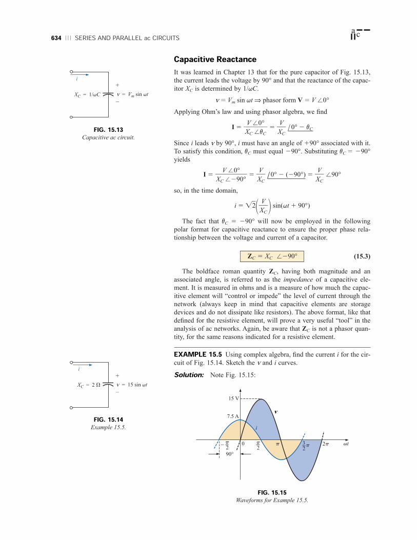
634 SERIES AND PARALLEL ac CIRCUITS
Capacitive ReactanceIt was learned in Chapter 13 that for the pure capacitor of Fig. 15.13,
the current leads the voltage by 90° and that the reactance of the capac-
itor XC is determined by 1/qC.
v 5 Vm sin qt ⇒ phasor form V 5 V /0°
Applying Ohm’s law and using phasor algebra, we find
I 5 5 /0° 2 vC
Since i leads v by 90°, i must have an angle of 190° associated with it.
To satisfy this condition, vC must equal 290°. Substituting vC 5 290°
yields
I 5 5 /0° 2 (290°) 5 /90°
so, in the time domain,
i 5 Ï2w1 2 sin(qt 1 90°)
The fact that vC 5 290° will now be employed in the following
polar format for capacitive reactance to ensure the proper phase rela-
tionship between the voltage and current of a capacitor.
(15.3)
The boldface roman quantity ZC, having both magnitude and an
associated angle, is referred to as the impedance of a capacitive ele-
ment. It is measured in ohms and is a measure of how much the capac-
itive element will “control or impede” the level of current through the
network (always keep in mind that capacitive elements are storage
devices and do not dissipate like resistors). The above format, like that
defined for the resistive element, will prove a very useful “tool” in the
analysis of ac networks. Again, be aware that ZC is not a phasor quan-
tity, for the same reasons indicated for a resistive element.
EXAMPLE 15.5 Using complex algebra, find the current i for the cir-
cuit of Fig. 15.14. Sketch the v and i curves.
Solution: Note Fig. 15.15:
ZC 5 XC /290°
VXC
VXC
VXC
V /0°XC /290°
VXC
V /0°XC /vC
a c
v = 15 sin qt
+
–
XC = 2 V
i
FIG. 15.14Example 15.5.
15 V
0
7.5 A
2p p 3p 2p
v
i
90°2p–
2 tv
FIG. 15.15Waveforms for Example 15.5.
v = Vm sin qt
+
–
i
XC = 1/qC
FIG. 15.13Capacitive ac circuit.

The phasor diagrams for the two circuits of the two preceding exam-
ples are shown in Fig. 15.18. Both indicate quite clearly that the current
i leads the voltage v by 90°.
+
j
I
V
10.605 V
Leading5.303 A
+
j
Leading
V
I
60°2.121 V
4.242 A
(a) (b)
IMPEDANCE AND THE PHASOR DIAGRAM 635
v 5 15 sin qt ⇒ phasor notation V 5 10.605 V /0°
I 5 5 5 5 5.303 A /90°
and i 5 Ï2w(5.303) sin(qt 1 90°) 5 7.5 sin(qt 1 90°)
EXAMPLE 15.6 Using complex algebra, find the voltage v for the cir-
cuit of Fig. 15.16. Sketch the v and i curves.
Solution: Note Fig. 15.17:
i 5 6 sin(qt 2 60°) ⇒ phasor notation I 5 4.242 A /260°
V5 IZC 5 (I /v)(XC /290°) 5 (4.242 A /260°)(0.5 V /290°)
5 2.121 V /2150°
and v 5 Ï2w(2.121) sin(qt 2 150°) 5 3.0 sin(qt 2 150°)
10.605 V /0°
2 V /290°
V /vXC /290°
VZC
a c
v+
–XC = 0.5 V
i = 6 sin(qt – 60°)
FIG. 15.16Example 15.6.
3 V
0
6 A
p
v
i
90°60°
tv3p5p2
2p2p 3p
2
FIG. 15.18Phasor diagrams for Examples 15.5 and 15.6.
Impedance DiagramNow that an angle is associated with resistance, inductive reactance,
and capacitive reactance, each can be placed on a complex plane dia-
FIG. 15.17Waveforms for Example 15.6.
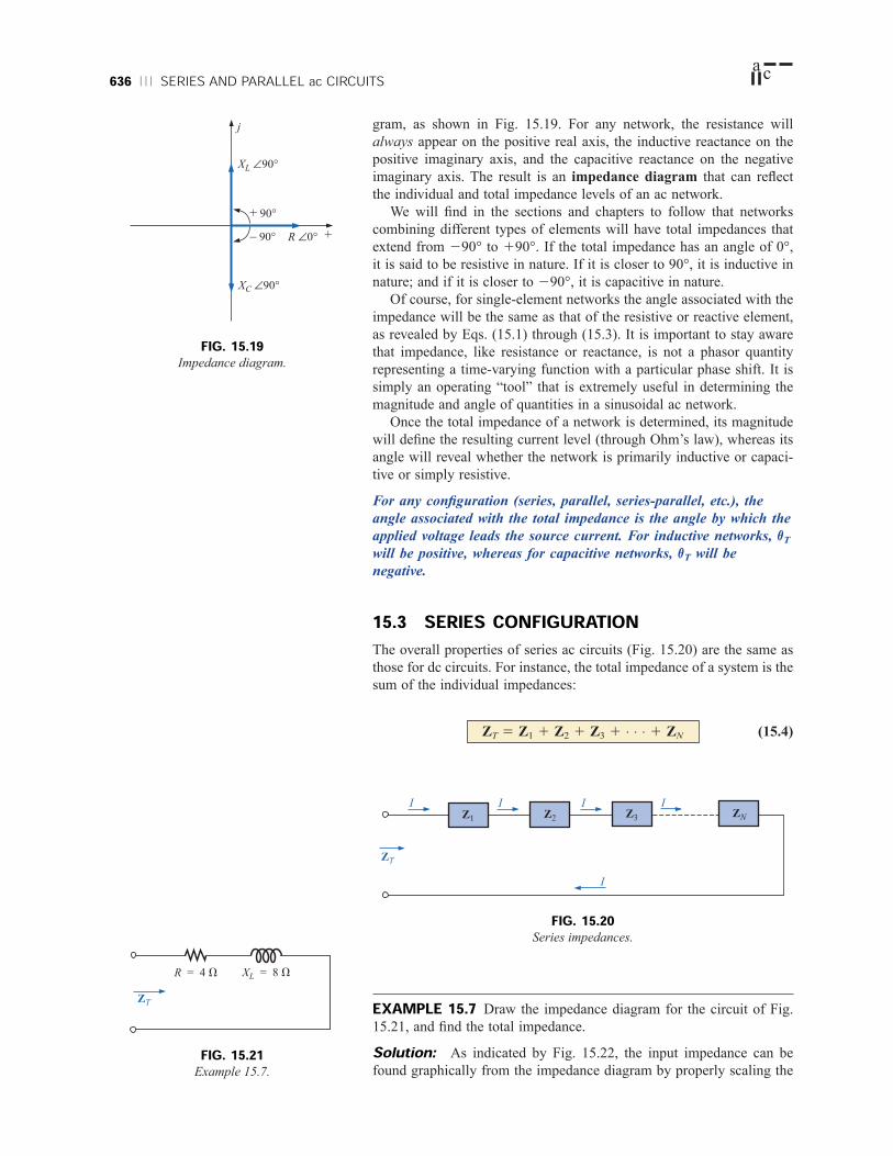
636 SERIES AND PARALLEL ac CIRCUITS
gram, as shown in Fig. 15.19. For any network, the resistance will
always appear on the positive real axis, the inductive reactance on the
positive imaginary axis, and the capacitive reactance on the negative
imaginary axis. The result is an impedance diagram that can reflect
the individual and total impedance levels of an ac network.
We will find in the sections and chapters to follow that networks
combining different types of elements will have total impedances that
extend from 290° to 190°. If the total impedance has an angle of 0°,
it is said to be resistive in nature. If it is closer to 90°, it is inductive in
nature; and if it is closer to 290°, it is capacitive in nature.
Of course, for single-element networks the angle associated with the
impedance will be the same as that of the resistive or reactive element,
as revealed by Eqs. (15.1) through (15.3). It is important to stay aware
that impedance, like resistance or reactance, is not a phasor quantity
representing a time-varying function with a particular phase shift. It is
simply an operating “tool” that is extremely useful in determining the
magnitude and angle of quantities in a sinusoidal ac network.
Once the total impedance of a network is determined, its magnitude
will define the resulting current level (through Ohm’s law), whereas its
angle will reveal whether the network is primarily inductive or capaci-
tive or simply resistive.
For any configuration (series, parallel, series-parallel, etc.), the
angle associated with the total impedance is the angle by which the
applied voltage leads the source current. For inductive networks, vT
will be positive, whereas for capacitive networks, vT will be
negative.
15.3 SERIES CONFIGURATIONThe overall properties of series ac circuits (Fig. 15.20) are the same as
those for dc circuits. For instance, the total impedance of a system is the
sum of the individual impedances:
(15.4)ZT 5 Z1 1 Z2 1 Z3 1 ⋅ ⋅ ⋅ 1 ZN
a c
I
ZT
I I IZNZ3Z2Z1
I
FIG. 15.20Series impedances.
EXAMPLE 15.7 Draw the impedance diagram for the circuit of Fig.
15.21, and find the total impedance.
Solution: As indicated by Fig. 15.22, the input impedance can be
found graphically from the impedance diagram by properly scaling the
R = 4 V XL = 8 V
ZT
FIG. 15.21Example 15.7.
+ 90°
j
– 90°
XL ∠90°
XC ∠90°
R ∠0° +
FIG. 15.19Impedance diagram.

XL = 8 V
j
Z T
+R = 4 V
vT
FIG. 15.22Impedance diagram for Example 15.7.
+
j
ZT
Tθ
R = 6 Ω
XL = 10 Ω
XC – XL = 2 Ω
XC = 12 Ω
SERIES CONFIGURATION 637
real and imaginary axes and finding the length of the resultant vector ZT
and angle vT. Or, by using vector algebra, we obtain
ZT 5 Z1 1 Z2
5 R /0° 1 XL /90°
5 R 1 jXL 5 4 V 1 j8 V
ZT 5 8.944 V /63.43°
EXAMPLE 15.8 Determine the input impedance to the series network
of Fig. 15.23. Draw the impedance diagram.
Solution:ZT 5 Z1 1 Z2 1 Z3
5 R /0° 1 XL /90° 1 XC /290°
5 R 1 jXL 2 jXC
5 R 1 j(XL 2 XC) 5 6 V 1 j(10 V 2 12 V) 5 6 V 2 j2 V
ZT 5 6.325 V /218.43°
The impedance diagram appears in Fig. 15.24. Note that in this
example, series inductive and capacitive reactances are in direct oppo-
sition. For the circuit of Fig. 15.23, if the inductive reactance were
equal to the capacitive reactance, the input impedance would be purely
resistive. We will have more to say about this particular condition in a
later chapter.
For the representative series ac configuration of Fig. 15.25 having
two impedances, the current is the same through each element (as it
was for the series dc circuits) and is determined by Ohm’s law:
ZT 5 Z1 1 Z2
and (15.5)
The voltage across each element can then be found by another applica-
tion of Ohm’s law:
(15.6a)
(15.6b)
Kirchhoff’s voltage law can then be applied in the same manner as it
is employed for dc circuits. However, keep in mind that we are now
dealing with the algebraic manipulation of quantities that have both
magnitude and direction.
E 2 V1 2 V2 5 0
or (15.7)
The power to the circuit can be determined by
(15.8)
where vT is the phase angle between E and I.
P 5 EI cos vT
E 5 V1 1 V2
V2 5 IZ2
V1 5 IZ1
I 5 Z
E
T
a c
ZT
Z1
R = 6 V
Z2
XL = 10 V
Z3
XC = 12 V
FIG. 15.23Example 15.8
FIG. 15.24Impedance diagram for Example 15.8.
I
Z2
Z1
+
V2
–
V1 –+
E
+
ZT–
FIG. 15.25Series ac circuit.
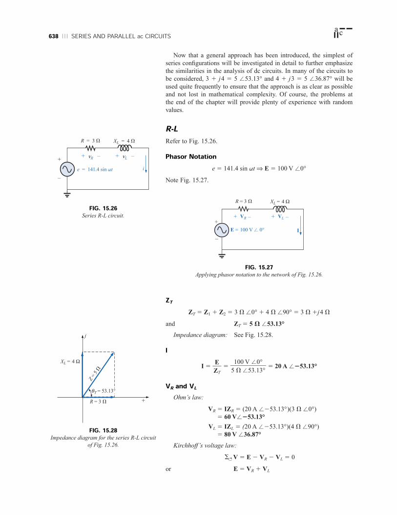
+
j
R = 3 V
XL = 4 Ω
Z = 5
V
Tθ = 53.13°
+
–
I
R = 3 V XL = 4 Ω
VR+ – VL+ –
E = 100 V / 0°
638 SERIES AND PARALLEL ac CIRCUITS
Now that a general approach has been introduced, the simplest of
series configurations will be investigated in detail to further emphasize
the similarities in the analysis of dc circuits. In many of the circuits to
be considered, 3 1 j4 5 5 /53.13° and 4 1 j3 5 5 /36.87° will be
used quite frequently to ensure that the approach is as clear as possible
and not lost in mathematical complexity. Of course, the problems at
the end of the chapter will provide plenty of experience with random
values.
R-LRefer to Fig. 15.26.
Phasor Notatione 5 141.4 sin qt ⇒ E 5 100 V /0°
Note Fig. 15.27.
a c
R = 3 V XL = 4 V
vL –+vR –+
–
+
e = 141.4 sin qt i
FIG. 15.26Series R-L circuit.
FIG. 15.27Applying phasor notation to the network of Fig. 15.26.
FIG. 15.28Impedance diagram for the series R-L circuit
of Fig. 15.26.
ZTZT 5 Z1 1 Z2 5 3 V /0° 1 4 V /90° 5 3 V 1j4 V
and ZT 5 5 V /53.13°
Impedance diagram: See Fig. 15.28.
II 5 5 5 20 A /253.13°
VR and VLOhm’s law:
VR 5 IZR 5 (20 A /253.13°)(3 V /0°)
5 60 V/253.13°
VL 5 IZL 5 (20 A /253.13°)(4 V /90°)
5 80 V /36.87°
Kirchhoff’s voltage law:
V 5 E 2 VR 2 VL 5 0
or E 5 VR 1 VL
S
100 V /0°5 V /53.13°
EZT

+
j
80 V
60 V
VR
I
53.13° E
VL
36.87°100 V
SERIES CONFIGURATION 639
In rectangular form,
VR 5 60 V /253.13° 5 36 V 2 j 48 V
VL 5 80 V /136.87° 5 64 V 1 j 48 V
and
E 5 VR 1 VL 5 (36 V 2 j 48 V) 1 (64 V 1 j 48 V) 5 100 V 1 j 0
5 100 V /0°
as applied.
Phasor diagram: Note that for the phasor diagram of Fig. 15.29, I
is in phase with the voltage across the resistor and lags the voltage
across the inductor by 90°.
Power: The total power in watts delivered to the circuit is
PT 5 EI cos vT
5 (100 V)(20 A) cos 53.13° 5 (2000 W)(0.6)
5 1200 W
where E and I are effective values and vT is the phase angle between E
and I, or
PT 5 I2R
5 (20 A)2(3 V) 5 (400)(3)
5 1200 W
where I is the effective value, or, finally,
PT 5 PR 1 PL 5 VRI cos vR 1 VLI cos vL
5 (60 V)(20 A) cos 0° 1 (80 V)(20 A) cos 90°
5 1200 W 1 0
5 1200 W
where vR is the phase angle between VR and I, and vL is the phase angle
between VL and I.
Power factor: The power factor Fp of the circuit is cos 53.13° 5
0.6 lagging, where 53.13° is the phase angle between E and I.
If we write the basic power equation P 5 EI cos v as follows:
cos v 5
where E and I are the input quantities and P is the power delivered to
the network, and then perform the following substitutions from the
basic series ac circuit:
cos v 5 5 5 5 5
we find (15.9)
Reference to Fig. 15.28 also indicates that v is the impedance angle
vT as written in Eq. (15.9), further supporting the fact that the imped-
ance angle vT is also the phase angle between the input voltage and cur-
rent for a series ac circuit. To determine the power factor, it is necessary
Fp 5 cos vT 5 Z
R
T
RZT
RE/I
IRE
I2REI
PEI
PEI
a c
FIG. 15.29Phasor diagram for the series R-L circuit of
Fig. 15.26.

+
30 V
VR
E
VC
53.13°36.87°
I 50 V
j
40 V
+
j
Tθ = 53.13°
R = 6 V
ZT =
10 ΩXC = 8 Ω
R = 6 V
VR+ –
XC = 8 Ω
VC+ –I = 5 /53.13°
I E+
–
ZT
640 SERIES AND PARALLEL ac CIRCUITS
only to form the ratio of the total resistance to the magnitude of the
input impedance. For the case at hand,
Fp 5 cos v 5 5 5 0.6 lagging
as found above.
R-CRefer to Fig. 15.30.
Phasor Notationi 5 7.07 sin(qt 1 53.13°) ⇒ I 5 5 A /53.13°
Note Fig. 15.31.
3 V5 V
RZT
a c
FIG. 15.31Applying phasor notation to the circuit of Fig. 15.30.
ZTZT 5 Z1 1 Z2 5 6 V /0° 1 8 V /290° 5 6 V 2 j8 V
and ZT 5 10 V /253.13°
Impedance diagram: As shown in Fig. 15.32.
EE 5 IZT 5 (5 A /53.13°)(10 V /253.13°) 5 50 V /0°
VR and VCVR 5 IZR 5 (I /v)(R /0°) 5 (5 A /53.13°)(6 V /0°)
5 30 V /53.13°
VC 5 IZC 5 (I /v)(XC /290°) 5 (5 A /53.13°)(8 V /290°)
5 40 V /236.87°
Kirchhoff’s voltage law:
V 5 E 2 VR 2 VC 5 0
or E 5 VR 1 VC
which can be verified by vector algebra as demonstrated for the R-L
circuit.
Phasor diagram: Note on the phasor diagram of Fig. 15.33 that the
current I is in phase with the voltage across the resistor and leads the
voltage across the capacitor by 90°.
S
FIG. 15.32Impedance diagram for the series R-C circuit
of Fig. 15.30.
FIG. 15.33Phasor diagram for the series R-C circuit
of Fig. 15.30.
R = 6 V XC = 8 V
vC –+vR –+
i = 7.07 sin(qt + 53.13°)
FIG. 15.30Series R-C ac circuit.

SERIES CONFIGURATION 641a c
70.70 V
56.56 V
42.42 VvR
e
vC
36.87°
90°
ip0 tv
p2p
23
p
2p
2–
Power: The total power in watts delivered to the circuit is
PT 5 EI cos vT 5 (50 V)(5 A) cos 53.13°
5 (250)(0.6) 5 150 W
or PT 5 I2R 5 (5 A)2(6 V) 5 (25)(6)
5 150 W
or, finally,
PT 5 PR 1 PC 5 VRI cos vR 1 VC I cos vC
5 (30 V)(5 A) cos 0° 1 (40 V)(5 A) cos 90°
5 150 W 1 0
5 150 W
Power factor: The power factor of the circuit is
Fp 5 cos v 5 cos 53.13° 5 0.6 leading
Using Eq. (15.9), we obtain
Fp 5 cos v 5 5
5 0.6 leading
as determined above.
6 V10 V
RZT
FIG. 15.34Waveforms for the series R-C circuit of Fig. 15.30.
Time domain: In the time domain,
e 5 Ï2w(50) sin qt 5 70.70 sin qt
vR 5 Ï2w(30) sin(qt 1 53.13°) 5 42.42 sin(qt 1 53.13°)
vC 5 Ï2w(40) sin(qt 2 36.87°) 5 56.56 sin(qt 2 36.87°)
A plot of all of the voltages and the current of the circuit appears
in Fig. 15.34. Note again that i and vR are in phase and that vC lags i
by 90°.

+
j
XL = 7 Ω
XL – XC = 4 Ω
XC = 3 Ω
R = 3 Ω
Z T =
5Ω
θT = 53.13°
642 SERIES AND PARALLEL ac CIRCUITS
R-L-CRefer to Fig. 15.35.
a c
R = 3 V XC = 3 V
VC –+VR –+
E = 50 V ∠ 0°
VL –+
XL = 7 V
–
+
I
ZTZT 5 Z1 1 Z2 1 Z35 R /0° 1 XL /90° 1 XC /290°
5 3 V 1 j 7 V 2 j 3 V 5 3 V 1 j 4 V
and ZT 5 5 V /53.13°
Impedance diagram: As shown in Fig. 15.37.
II 5 5 5 10 A /253.13°
VR,VL, and VCVR 5 IZR 5 (I /v)(R /0°) 5 (10 A /253.13°)(3 V /0°)
5 30 V /253.13°
VL 5 IZL 5 (I /v)(XL /90°) 5 (10 A /253.13°)(7 V /90°)
5 70 V /36.87°
VC 5 IZC 5 (I /v)(XC /290°) 5 (10 A /253.13°)(3 V /290°)
5 30 V /2143.13°
Kirchhoff’s voltage law:
V 5 E 2 VR 2 VL 2 VC 5 0S
50 V /0°5 V /53.13°
EZT
FIG. 15.36Applying phasor notation to the circuit of Fig. 15.35.
FIG. 15.37Impedance diagram for the series R-L-C
circuit of Fig. 15.35.
R = 3 V XC = 3 V
vC –+vR –+
e = 70.7 sin qt
vL –+
XL = 7 V
–
+
i
FIG. 15.35Series R-L-C ac circuit.
Phasor Notation As shown in Fig. 15.36.

V L – V C
VC
VL
E
36.87°
53.13°I
j
+
VR
SERIES CONFIGURATION 643a c
FIG. 15.38Phasor diagram for the series R-L-C circuit of
Fig. 15.35.
or E 5 VR 1 VL 1 VC
which can also be verified through vector algebra.
Phasor diagram: The phasor diagram of Fig. 15.38 indicates that
the current I is in phase with the voltage across the resistor, lags the
voltage across the inductor by 90°, and leads the voltage across the
capacitor by 90°.
Time domain:
i 5 Ï2w(10) sin(qt 2 53.13°) 5 14.14 sin(qt 2 53.13°)
vR 5 Ï2w(30) sin(qt 253.13°) 5 42.42 sin(qt 2 53.13°)
vL 5 Ï2w(70) sin(qt 1 36.87°) 5 98.98 sin(qt 1 36.87°)
vC 5 Ï2w(30) sin(qt 2 143.13°) 5 42.42 sin(qt 2 143.13°)
A plot of all the voltages and the current of the circuit appears in Fig.
15.39.
FIG. 15.39Waveforms for the series R-L circuit of Fig. 15.35.
98.98 V
70.70 V
42.42 V
vL
vC
53.13°90°
p0
36.87°
e
vR
i
tvp3p
25p2
p23p
2p
2–
Power: The total power in watts delivered to the circuit is
PT 5 EI cos vT 5 (50 V)(10 A) cos 53.13° 5 (500)(0.6) 5 300 W
or PT 5 I2R 5 (10 A)2(3 V) 5 (100)(3) 5 300 W
or
PT 5 PR 1 PL 1 PC
5 VRI cos vR 1 VLI cos vL 1 VC I cos vC
5 (30 V)(10 A) cos 0° 1 (70 V)(10 A) cos 90° 1 (30 V)(10 A) cos 90°
5 (30 V)(10 A) 1 0 1 0 5 300 W
Power factor: The power factor of the circuit is
Fp 5 cos vT 5 cos 53.13° 5 0.6 lagging
Using Eq. (15.9), we obtain
Fp 5 cos v 5 5 5 0.6 lagging3 V5 V
RZT

a c
15.4 VOLTAGE DIVIDER RULEThe basic format for the voltage divider rule in ac circuits is exactly
the same as that for dc circuits:
(15.10)
where Vx is the voltage across one or more elements in series that have
total impedance Zx, E is the total voltage appearing across the series
circuit, and ZT is the total impedance of the series circuit.
EXAMPLE 15.9 Using the voltage divider rule, find the voltage across
each element of the circuit of Fig. 15.40.
Solution:VC 5 5 5
5 5 80 V /236.87°
VR 5 5 5
5 60 V /153.13°
EXAMPLE 15.10 Using the voltage divider rule, find the unknown
voltages VR, VL, VC, and V1 for the circuit of Fig. 15.41.
300 /0°5 /253.13°
(3 V /0°)(100 V /0°)
5 V /253.13°
ZREZC 1 ZR
400 /290°5 /253.13°
400 /290°
3 2 j 4
(4 V /290°)(100 V /0°)
4 V /290° 1 3 V /0°
ZCEZC 1 ZR
Vx 5 Z
Zx
T
E
644 SERIES AND PARALLEL ac CIRCUITS
R = 6 V XC = 17 V
VC –+VR –+
E = 50 V ∠ 30°–
+
V1
XL = 9 V
VL –+
Solution:VR 5 5
5 5
5 5 30 V /83.13°
Calculator The above calculation provides an excellent opportunity
to demonstrate the power of today’s calculators. Using the notation of
the TI-86 calculator, the above calculation and the result are as follows:
300 /30°10 /253.13°
300 /30°
6 2 j 8
300 /30°6 1 j 9 2 j 17
(6 V /0°)(50 V /30°)6 V /0° 1 9 V /90° 1 17 V /290°
ZREZR 1 ZL 1 ZC
FIG. 15.41Example 15.10.
R = 3 V XC = 4 V
VC –+VR –+
E = 100 V ∠ 0°–
+
FIG. 15.40Example 15.9.

VOLTAGE DIVIDER RULE 645
CALC. 15.1
VL 5 5 5
5 45 V /173.13°
VC 5 5 5
5 85 V /26.87°
V1 5 5
5
5 5 40 V /26.87°
EXAMPLE 15.11 For the circuit of Fig. 15.42:
400 /260°10 /253.13°
(8 /290°)(50 /30°)
10 /253.13°
(9 V /90° 1 17 V /290°)(50 V /30°)
10 V /253.13°
(ZL 1 ZC)E
ZT
850 V/260°
10 /253°
(17 V /290°)(50 V /30°)
10 V /253.13°
ZCEZT
450 V/120°10 /253.13°
(9 V /90°)(50 V /30°)
10 V /253.13°
ZLEZT
a c
R1 = 6 V L2 = 0.05 H
vC–+–+
e = =2(20) sin 377t
–
+ vL–+
L1 = 0.05 H
vR
R2 = 4 V
C2 = 200 mFC1 = 200 mF
i
FIG. 15.42Example 15.11.
a. Calculate I, VR, VL, and VC in phasor form.
b. Calculate the total power factor.
c. Calculate the average power delivered to the circuit.
d. Draw the phasor diagram.
e. Obtain the phasor sum of VR, VL, and VC, and show that it equals the
input voltage E.
f. Find VR and VC using the voltage divider rule.
Solutions:a. Combining common elements and finding the reactance of the
inductor and capacitor, we obtain
RT 5 6 V 1 4 V 5 10 V
LT 5 0.05 H 1 0.05 H 5 0.1 H
CT 5 5 100 mF200 mF
2
(6/0)*(50/30)/((6/0)1(9/90)1(17/290))(3.588E0,29.785E0)
Ans c Pol(30.000E0/83.130E0)
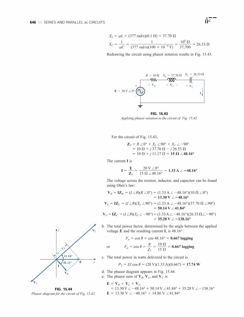
VC
VL
E
41.84°
48.16°I
j
+
VR
VL –
VC
646 SERIES AND PARALLEL ac CIRCUITSa c
XL 5 qL 5 (377 rad/s)(0.1 H) 5 37.70 V
XC 5 5 5 5 26.53 V
Redrawing the circuit using phasor notation results in Fig. 15.43.
106V
37,700
1(377 rad/s)(100 3 1026 F)
1qC
FIG. 15.44Phasor diagram for the circuit of Fig. 15.42.
FIG. 15.43Applying phasor notation to the circuit of Fig. 15.42.
R = 10 V XC = 26.53 V
VC –+VR –+
E = 20 V ∠ 0°–
+
I
XL = 37.70 V
VL –+
For the circuit of Fig. 15.43,
ZT 5 R /0° 1 XL /90° 1 XC /290°
5 10 V 1 j 37.70 V 2 j 26.53 V
5 10 V 1 j 11.17 V 5 15 V /48.16°
The current I is
I 5 5 5 1.33 A /248.16°
The voltage across the resistor, inductor, and capacitor can be found
using Ohm’s law:
VR 5 IZR 5 (I /v)(R /0°) 5 (1.33 A /248.16°)(10 V /0°)
5 13.30 V /248.16°
VL 5 IZL 5 (I /v)(XL /90°) 5 (1.33 A /248.16°)(37.70 V /90°)
5 50.14 V /41.84°
VC 5 IZC 5 (I /v)(XC /290°) 5 (1.33A /248.16°)(26.53 V/290°)
5 35.28 V /2138.16°
b. The total power factor, determined by the angle between the applied
voltage E and the resulting current I, is 48.16°:
Fp 5 cos v 5 cos 48.16° 5 0.667 lagging
or Fp 5 cos v 5 5 5 0.667 lagging
c. The total power in watts delivered to the circuit is
PT 5 EI cos v 5 (20 V)(1.33 A)(0.667) 5 17.74 W
d. The phasor diagram appears in Fig. 15.44.
e. The phasor sum of VR, VL, and VC is
E 5 VR 1 VL 1 VC
5 13.30 V /248.16° 1 50.14 V /41.84° 1 35.28 V /2138.16°
E 5 13.30 V /248.16° 1 14.86 V /41.84°
10 V15 V
RZT
20 V /0°15 V /48.16°
EZT

FREQUENCY RESPONSE OF THE R-C CIRCUIT 647
Therefore,
E 5 Ï(1w3w.3w0w Vw)2w 1w (w1w4w.8w6w Vw)2w 5 20 V
and vE 5 0° (from phasor diagram)
and E 5 20 /0°
f. VR 5 5 5
5 13.3 V /248.16°
VC 5 5 5
5 35.37 V /2138.16°
15.5 FREQUENCY RESPONSE OF THER-C CIRCUITThus far, the analysis of series circuits has been limited to a particular
frequency. We will now examine the effect of frequency on the response
of an R-C series configuration such as that in Fig. 15.45. The magnitude
of the source is fixed at 10 V, but the frequency range of analysis will
extend from zero to 20 kHz.
530.6 V/290°
15 /48.16°
(26.5 V /290°)(20 V /0°)
15 V /48.16°
ZCEZT
200 V/0°15 /48.16°
(10 V /0°)(20 V /0°)
15 V /48.16°
ZREZT
a c
5 kV
ZTE = 10 V ∠ 0°–
+
R
C 0.01 mF
–
+
VC
f : 0 to 20 kHz
FIG. 15.45Determining the frequency response of a series R-C circuit.
ZT Let us first determine how the impedance of the circuit ZT will
vary with frequency for the specified frequency range of interest.
Before getting into specifics, however, let us first develop a sense for
what we should expect by noting the impedance-versus-frequency
curve of each element, as drawn in Fig. 15.46.
At low frequencies the reactance of the capacitor will be quite high
and considerably more than the level of the resistance R, suggesting that
the total impedance will be primarily capacitive in nature. At high fre-
quencies the reactance XC will drop below the R 5 5-kV level, and the
network will start to shift toward one of a purely resistive nature (at
5 kV). The frequency at which XC 5 R can be determined in the fol-
lowing manner:
XC 5 5 R
andXC 5 R
(15.11)f1 5 2p
1
RC
12pf1C

648 SERIES AND PARALLEL ac CIRCUITS
which for the network of interest is
f1 5 > 3183.1 Hz
For frequencies less than f1, XC > R, and for frequencies greater than f1,
R > XC, as shown in Fig. 15.46.
Now for the details. The total impedance is determined by the fol-
lowing equation:
ZT 5 R 2 j XC
and (15.12)
The magnitude and angle of the total impedance can now be found
at any frequency of interest by simply substituting into Eq. (15.12). The
presence of the capacitor suggests that we start from a low frequency
(100 Hz) and then open the spacing until we reach the upper limit of
interest (20 kHz).
f 5 100 Hz
XC 5 5 5 159.16 kV
and ZT 5 ÏRw2w1w Xw2Cw 5 Ï(5w kwVw)2w 1w (w1w5w9w.1w6w kwVw)2w 5 159.24 kV
with vT 5 2tan215 2tan21
5 2tan21 31.83
5 288.2°
and ZT 5 159.24 kV /288.2°
which compares very closely with ZC 5 159.16 kV /290° if the cir-
cuit were purely capacitive (R 5 0 V). Our assumption that the circuit
is primarily capacitive at low frequencies is therefore confirmed.
159.16 kV
5 kV
XCR
12p(100 Hz)(0.01 mF)
12pfC
ZT 5 ZT /vT 5 ÏRw2w1w Xw2Cw /2tan21
X
RC
12p(5 kV)(0.01 mF)
a c
0
R = 5 kV
ZT XC = 12 fC
f
5 kV
R
XC
5 kV
R < XC R > XC
0 f
p
f1
FIG. 15.46The frequency response of the individual elements of a series R-C circuit.

FREQUENCY RESPONSE OF THE R-C CIRCUIT 649
f 5 1 kHz
XC 5 5 5 15.92 kV
and ZT 5 ÏRw2w1w Xw2Cw 5 Ï(5w kwVw)2w 1w (w1w5w.9w2w kwVw)2w 5 16.69 kV
with vT 5 2tan215 2tan21
5 2tan21 3.18 5 272.54°
and ZT 5 16.69 kV /272.54°
A noticeable drop in the magnitude has occurred, and the impedance
angle has dropped almost 17° from the purely capacitive level.
Continuing:
f 5 5 kHz: ZT 5 5.93 kV /232.48°
f 5 10 kHz: ZT 5 5.25 kV /217.66°
f 5 15 kHz: ZT 5 5.11 kV /211.98°
f 5 20 kHz: ZT 5 5.06 kV /29.04°
Note how close the magnitude of ZT at f 5 20 kHz is to the resistance
level of 5 kV. In addition, note how the phase angle is approaching that
associated with a pure resistive network (0°).
A plot of ZT versus frequency in Fig. 15.47 completely supports our
assumption based on the curves of Fig. 15.46. The plot of vT versus fre-
quency in Fig. 15.48 further suggests the fact that the total impedance
made a transition from one of a capacitive nature (vT 5 290°) to one
with resistive characteristics (vT 5 0°).
15.92 kV
5 kV
XCR
12p(1 kHz)(0.01 mF)
12pfC
a c
50 101 15 20 f (kHz)
Circuit resistive
Circuit capacitive
5
10
15
20
ZT (kV)
R = 5 kV
ZT ( f )
FIG. 15.47The magnitude of the input impedance versus frequency for the circuit of
Fig. 15.45.

650 SERIES AND PARALLEL ac CIRCUITS
Applying the voltage divider rule to determine the voltage across the
capacitor in phasor form yields
VC 5
5 5
5
or VC 5VC /vC 5 /290° 1 tan21(XC/R)
The magnitude of VC is therefore determined by
VC 5 (15.13)
and the phase angle vC by which VC leads E is given by
(15.14)
To determine the frequency response, XC must be calculated for each
frequency of interest and inserted into Eqs. (15.13) and (15.14).
To begin our analysis, it makes good sense to consider the case of
f 5 0 Hz (dc conditions).
vC 5 290° 1 tan21X
R
C 5 2tan21
X
R
C
XCEÏRw2w1w Xw2
Cw
XC EÏRw2w1w Xw2
Cw
XC E /290°ÏRw2w1w Xw2
Cw /2tan21 XC/R
XC E /290°
R 2 j XC
(XC /290°)(E /0°)
R 2 j XC
ZCEZR 1 ZC
a c
5
0°
101 15 20 f (kHz)
Circuit capacitive
–45°
–30°
–60°
–90°
Circuit resistive
Tθ
T ( f )θ
FIG. 15.48The phase angle of the input impedance versus frequency for the circuit of
Fig. 15.45.

FREQUENCY RESPONSE OF THE R-C CIRCUIT 651
f 5 0 HzXC 5 5 ⇒ very large value
Applying the open-circuit equivalent for the capacitor based on the
above calculation will result in the following:
VC 5 E 5 10 V /0°
If we apply Eq. (15.13), we find
X2C >> R2
and ÏRw2w1w Xw2Cw > ÏXw2
Cw 5 XC
and VC 5 5 5 E
with vC 5 2tan215 2tan21 0 5 0°
verifying the above conclusions.
f 5 1 kHz Applying Eq. (15.13):
XC 5 5 > 15.92 kV
ÏRw2w1w Xw2Cw 5 Ï(5w kwVw)2w 1w (w1w5w.9w2w kwVw)2w > 16.69 kV
and VC 5 5 5 9.54 V
Applying Eq. (15.14):
vC 5 2tan215 2tan21
5 2tan21 0.314 5 217.46°
and VC 5 9.53 V /217.46°
As expected, the high reactance of the capacitor at low frequencies has
resulted in the major part of the applied voltage appearing across the
capacitor.
If we plot the phasor diagrams for f 5 0 Hz and f 5 1 kHz, as shown
in Fig. 15.49, we find that VC is beginning a clockwise rotation with an
increase in frequency that will increase the angle vC and decrease the
phase angle between I and E. Recall that for a purely capacitive net-
5 kV15.9 kV
RXC
(15.92 kV)(10)
16.69 kV
XCEÏRw2w1w Xw2
Cw
1(2p)(1 3 103 Hz)(0.01 3 1026 F)
12pfC
RXC
XCEXC
XCEÏRw2w1w Xw2
Cw
10
12p(0)C
a c
I = 0 A
f = 0 Hz
E
VCE
I
VR
f = 1 kHz
–17.46°
VC
Cθ
Iθ
C = 0°θ I = 90°θ
FIG. 15.49The phasor diagram for the circuit of Fig. 15.45 for f 5 0 Hz and 1 kHz.
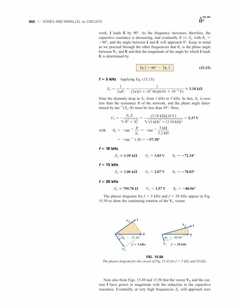
652 SERIES AND PARALLEL ac CIRCUITS
work, I leads E by 90°. As the frequency increases, therefore, the
capacitive reactance is decreasing, and eventually R >> XC with vC 5
290°, and the angle between I and E will approach 0°. Keep in mind
as we proceed through the other frequencies that vC is the phase angle
between VC and E and that the magnitude of the angle by which I leads
E is determined by
(15.15)
f 5 5 kHz Applying Eq. (15.13):
XC 5 5 > 3.18 kV
Note the dramatic drop in XC from 1 kHz to 5 kHz. In fact, XC is now
less than the resistance R of the network, and the phase angle deter-
mined by tan21(XC /R) must be less than 45°. Here,
VC 5 5 5 5.37 V
with vC 5 2tan215 2tan21
5 2tan21 1.56 5 257.38°
f 5 10 kHzXC > 1.59 kV VC 5 3.03 V vC 5 272.34°
f 5 15 kHzXC > 1.06 kV VC 5 2.07 V vC 5 278.02°
f 5 20 kHzXC > 795.78 V VC 5 1.57 V vC 5 280.96°
The phasor diagrams for f 5 5 kHz and f 5 20 kHz appear in Fig.
15.50 to show the continuing rotation of the VC vector.
5 kV3.2 kV
RXC
(3.18 kV)(10 V)
Ï(5w kwVw)2w 1w (w3w.1w8w kwVw)2wXCE
ÏRw2w1w Xw2
Cw
1(2p)(5 3 103 Hz)(0.01 3 1026 F)
12pfC
vI 5 90° 2 vC
a c
I
IVR
f = 20 kHz
VR
E
VC
f = 5 kHz
E
VC
C = –80.96°θ C = –57.38°θ
FIG. 15.50The phasor diagram for the circuit of Fig. 15.45 for f 5 5 kHz and 20 kHz.
Note also from Figs. 15.49 and 15.50 that the vector VR and the cur-
rent I have grown in magnitude with the reduction in the capacitive
reactance. Eventually, at very high frequencies XC will approach zero
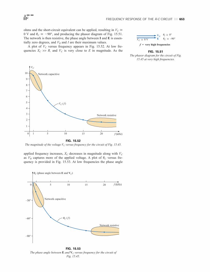
FREQUENCY RESPONSE OF THE R-C CIRCUIT 653a c
VC ≅ 0 V E
VRvI ≅ 0°vC ≅ –90°
f = very high frequencies
FIG. 15.51The phasor diagram for the circuit of Fig.
15.45 at very high frequencies.
50 101 15 20 f (kHz)
Network resistive
Network capacitive
4
9
10
VC
VC ( f )
8
7
6
5
3
2
1
ohms and the short-circuit equivalent can be applied, resulting in VC >0 V and vC > 290°, and producing the phasor diagram of Fig. 15.51.
The network is then resistive, the phase angle between I and E is essen-
tially zero degrees, and VR and I are their maximum values.
A plot of VC versus frequency appears in Fig. 15.52. At low fre-
quencies XC >> R, and VC is very close to E in magnitude. As the
FIG. 15.52The magnitude of the voltage VC versus frequency for the circuit of Fig. 15.45.
FIG. 15.53The phase angle between E and VC versus frequency for the circuit of
Fig. 15.45.
50 10 15 20 f (kHz)
Network capacitive–30°
–60°
–90°
Network resistive
1
C ( f )θ
C (phase angle between E and VC)θ
applied frequency increases, XC decreases in magnitude along with VC
as VR captures more of the applied voltage. A plot of vC versus fre-
quency is provided in Fig. 15.53. At low frequencies the phase angle

654 SERIES AND PARALLEL ac CIRCUITS
between VC and E is very small since VC > E. Recall that if two pha-
sors are equal, they must have the same angle. As the applied frequency
increases, the network becomes more resistive and the phase angle
between VC and E approaches 90°. Keep in mind that, at high frequen-
cies, I and E are approaching an in-phase situation and the angle
between VC and E will approach that between VC and I, which we
know must be 90° (IC leading VC).
A plot of VR versus frequency would approach E volts from zero
volts with an increase in frequency, but remember VR ? E 2 VC due to
the vector relationship. The phase angle between I and E could be plot-
ted directly from Fig. 15.53 using Eq. (15.15).
In Chapter 23, the analysis of this section will be extended to a much
wider frequency range using a log axis for frequency. It will be demon-
strated that an R-C circuit such as that in Fig. 15.45 can be used as a fil-
ter to determine which frequencies will have the greatest impact on the
stage to follow. From our current analysis, it is obvious that any net-
work connected across the capacitor will receive the greatest potential
level at low frequencies and be effectively “shorted out” at very high
frequencies.
The analysis of a series R-L circuit would proceed in much the same
manner, except that XL and VL would increase with frequency and the
angle between I and E would approach 90° (voltage leading the cur-
rent) rather than 0°. If VL were plotted versus frequency, VL would
approach E, and XL would eventually attain a level at which the open-
circuit equivalent would be appropriate.
15.6 SUMMARY: SERIES ac CIRCUITSThe following is a review of important conclusions that can be derived
from the discussion and examples of the previous sections. The list is
not all-inclusive, but it does emphasize some of the conclusions that
should be carried forward in the future analysis of ac systems.
For series ac circuits with reactive elements:
1. The total impedance will be frequency dependent.
2. The impedance of any one element can be greater than the total
impedance of the network.
3. The inductive and capacitive reactances are always in direct
opposition on an impedance diagram.
4. Depending on the frequency applied, the same circuit can be
either predominantly inductive or predominantly capacitive.
5. At lower frequencies the capacitive elements will usually have the
most impact on the total impedance, while at high frequencies the
inductive elements will usually have the most impact.
6. The magnitude of the voltage across any one element can be
greater than the applied voltage.
7. The magnitude of the voltage across an element compared to the
other elements of the circuit is directly related to the magnitude
of its impedance; that is, the larger the impedance of an
element, the larger the magnitude of the voltage across the
element.
8. The voltages across a coil or capacitor are always in direct
opposition on a phasor diagram.
9. The current is always in phase with the voltage across the
resistive elements, lags the voltage across all the inductive
a c

ADMITTANCE AND SUSCEPTANCE 655
elements by 90°, and leads the voltage across all the capacitive
elements by 90°.
10. The larger the resistive element of a circuit compared to the net
reactive impedance, the closer the power factor is to unity.
PARALLEL ac CIRCUITS
15.7 ADMITTANCE AND SUSCEPTANCEThe discussion for parallel ac circuits will be very similar to that for
dc circuits. In dc circuits, conductance (G) was defined as being equal
to 1/R. The total conductance of a parallel circuit was then found by
adding the conductance of each branch. The total resistance RT is sim-
ply 1/GT.
In ac circuits, we define admittance (Y) as being equal to 1/Z. The
unit of measure for admittance as defined by the SI system is siemens,
which has the symbol S. Admittance is a measure of how well an ac cir-
cuit will admit, or allow, current to flow in the circuit. The larger its
value, therefore, the heavier the current flow for the same applied
potential. The total admittance of a circuit can also be found by finding
the sum of the parallel admittances. The total impedance ZT of the cir-
cuit is then 1/YT; that is, for the network of Fig. 15.54:
(15.16)YT 5 Y1 1 Y2 1 Y3 1 ⋅ ⋅ ⋅ 1 YN
a c
Y1 =1
Z1Y2 =
1
Z2Y3 =
1
Z3YN =
1
ZN
YT
ZT
FIG. 15.54Parallel ac network.
or, since Z 5 1/Y,
(15.17)
For two impedances in parallel,
5 1
If the manipulations used in Chapter 6 to find the total resistance of two
parallel resistors are now applied, the following similar equation will
result:
(15.18)ZT 5 Z1
Z
1
1Z2
Z2
1Z2
1Z1
1ZT
Z
1
T
5 Z
1
1
1 Z
1
2
1 Z
1
3
1 ⋅ ⋅ ⋅ 1 Z
1
N

656 SERIES AND PARALLEL ac CIRCUITS
For three parallel impedances,
ZT 5 (15.19)
As pointed out in the introduction to this section, conductance is the
reciprocal of resistance, and
(15.20)
The reciprocal of reactance (1/X) is called susceptance and is a mea-
sure of how susceptible an element is to the passage of current through
it. Susceptance is also measured in siemens and is represented by the
capital letter B.
For the inductor,
(15.21)
Defining (siemens, S) (15.22)
we have (15.23)
Note that for inductance, an increase in frequency or inductance will
result in a decrease in susceptance or, correspondingly, in admittance.
For the capacitor,
(15.24)
Defining (siemens, S) (15.25)
we have (15.26)
For the capacitor, therefore, an increase in frequency or capacitance
will result in an increase in its susceptibility.
For parallel ac circuits, the admittance diagram is used with the
three admittances, represented as shown in Fig. 15.55.
Note in Fig. 15.55 that the conductance (like resistance) is on the
positive real axis, whereas inductive and capacitive susceptances are in
direct opposition on the imaginary axis.
For any configuration (series, parallel, series-parallel, etc.), the angle
associated with the total admittance is the angle by which the source
current leads the applied voltage. For inductive networks, vT is
negative, whereas for capacitive networks, vT is positive.
YC 5 BC /90°
BC 5 X
1
C
YC 5 Z
1
C
5 XC /
1
290° 5
X
1
C
/90°
YL 5 BL /290°
BL 5 X
1
L
YL 5 Z
1
L
5 XL /
1
90° 5
X
1
L
/290°
YR 5 Z
1
R
5 R /
1
0° 5 G /0°
Z1Z2Z3Z1Z2 1 Z2Z3 1 Z1Z3
a c
j
BC ∠ 90°
BL ∠ –90°
G ∠ 0°+
FIG. 15.55Admittance diagram.

XC 20 V
YT
ZT
R 5 V XL 8 V
XL 10 V
YT
ZT
R 20 V
ADMITTANCE AND SUSCEPTANCE 657
EXAMPLE 15.12 For the network of Fig. 15.56:
a. Find the admittance of each parallel branch.
b. Determine the input admittance.
c. Calculate the input impedance.
d. Draw the admittance diagram.
Solutions:a. YR 5 G /0° 5 /0° 5 /0°
5 0.05 S /0° 5 0.05 S 1 j 0
YL 5 BL /290° 5 /290° 5 /290°
5 0.1 S /290° 5 0 2 j 0.1 S
b. YT 5 YR 1 YL 5 (0.05 S 1 j 0) 1 (0 2 j 0.1 S)
5 0.05 S 2 j 0.1 S 5 G 2 j BL
c. ZT 5 5 5
5 8.93 V /63.43°
or Eq. (15.17):
ZT 5 5
5 5 8.93 V /63.43°
d. The admittance diagram appears in Fig. 15.57.
200 V /90°22.36 /26.57°
(20 V /0°)(10 V /90°)
20 V 1 j 10 V
ZRZLZR 1 ZL
10.112 S /263.43°
10.05 S 2 j 0.1 S
1YT
110 V
1XL
120 V
1R
a c
FIG. 15.56Example 15.12.
j
YT
+
YL = 0.1 S ∠ – 90°
0.112 S
–63.43°
YR = 0.05 S ∠ 0°
FIG. 15.57Admittance diagram for the network of
Fig. 15.56.
FIG. 15.58Example 15.13.
EXAMPLE 15.13 Repeat Example 15.12 for the parallel network of
Fig. 15.58.
Solutions:a. YR 5 G /0° 5 /0° 5 /0°
5 0.2 S /0° 5 0.2 S 1 j 0
15 V
1R

658 SERIES AND PARALLEL ac CIRCUITS
YL 5 BL /290° 5 /290° 5 /290°
5 0.125 S /290° 5 0 2 j 0.125 S
YC 5 BC /90° 5 /90° 5 /90°
5 0.050 S /190° 5 0 1 j 0.050 S
b. YT 5 YR 1 YL 1 YC
5 (0.2 S 1 j 0) 1 (0 2 j 0.125 S) 1 (0 1 j 0.050 S)
5 0.2 S 2 j 0.075 S 5 0.2136 S /220.56°
c. ZT 5 5 4.68 V /20.56°
or
ZT 5
5
1 (5 V /0°)(20 V /290°)
5
5 5
5
5 4.68 V /20.56°
d. The admittance diagram appears in Fig. 15.59.
On many occasions, the inverse relationship YT 5 1/ZT or ZT 5
1/YT will require that we divide the number 1 by a complex number
having a real and an imaginary part. This division, if not performed in
the polar form, requires that we multiply the numerator and denomina-
tor by the conjugate of the denominator, as follows:
YT 5 5 5 1 2 1 2 5
and YT 5 S 2 j S
To avoid this laborious task each time we want to find the reciprocal
of a complex number in rectangular form, a format can be developed
using the following complex number, which is symbolic of any imped-
ance or admittance in the first or fourth quadrant:
5 1 2 1 2 5
or (15.27)
Note that the denominator is simply the sum of the squares of each
term. The sign is inverted between the real and imaginary parts. A few
examples will develop some familiarity with the use of this equation.
a1 6
1
j b1
5 a2
1
a
1
1
b21
7 j a2
1
b
1
1
b21
a1 7 j b1a2
1 1 b21
a1 7 j b1a1 7 j b1
1a1 6 j b1
1a1 6 j b1
652
452
4 2 j 642
1 62
(4 V 2 j 6 V)(4 V 2 j 6 V)
14 V 1 j 6 V
14 V 1 j 6 V
1ZT
800 V170.88 /220.56°
800 V160 2 j 60
800 V160 1 j 40 2 j 100
800 V /0°40 /90° 1 160 /0° 1 100 /290°
(5 V /0°)(8 V /90°)(20 V /290°)(5 V /0°)(8 V /90°) 1 (8 V /90°)(20 V /290°)
ZRZLZCZRZL 1 ZLZC 1 ZRZC
10.2136 S /220.56°
120 V
1XC
18 V
1XL
a c
20.56°
YR
YC
YL – YC
YT
0.2136 S
+
YL
j
FIG. 15.59Admittance diagram for the network of
Fig. 15.58.
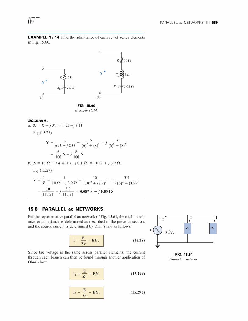
R 6 V
XC 8 V
Y
(a)
R 10 V
XC 0.1 V
Y
(b)
XL 4 V
PARALLEL ac NETWORKS 659a c
I
Z2EZT, YT
Z1
I1 I2
EXAMPLE 15.14 Find the admittance of each set of series elements
in Fig. 15.60.
FIG. 15.60Example 15.14.
FIG. 15.61Parallel ac network.
Solutions:a. Z 5 R 2 j XC 5 6 V 2j 8 V
Eq. (15.27):
Y 5 5 1 j
5 S 1 j S
b. Z 5 10 V 1 j 4 V 1 (2j 0.1 V) 5 10 V 1 j 3.9 V
Eq. (15.27):
Y 5 5 5 2 j
5 2 j 5 0.087 S 2 j 0.034 S
15.8 PARALLEL ac NETWORKSFor the representative parallel ac network of Fig. 15.61, the total imped-
ance or admittance is determined as described in the previous section,
and the source current is determined by Ohm’s law as follows:
(15.28)
Since the voltage is the same across parallel elements, the current
through each branch can then be found through another application of
Ohm’s law:
(15.29a)
(15.29b)I2 5 Z
E
2
5 EY2
I1 5 Z
E
1
5 EY1
I 5 Z
E
T
5 EYT
3.9115.21
10115.21
3.9(10)2
1 (3.9)2
10(10)2
1 (3.9)2
110 V 1 j 3.9 V
1Z
8100
6100
8(6)2
1 (8)2
6(6)2
1 (8)2
16 V 2 j 8 V

660 SERIES AND PARALLEL ac CIRCUITS
Kirchhoff’s current law can then be applied in the same manner as
employed for dc networks. However, keep in mind that we are now
dealing with the algebraic manipulation of quantities that have both
magnitude and direction.
I 2 I1 2 I2 5 0
or (15.30)
The power to the network can be determined by
(15.31)
where vT is the phase angle between E and I.
Let us now look at a few examples carried out in great detail for the
first exposure.
R-LRefer to Fig. 15.62.
P 5 EI cos vT
I 5 I1 1 I2
a c
YT and ZTYT 5 YR 1 YL
5 G /0° 1 BL /290° 5 /0° 1 /290°
5 0.3 S /0° 1 0.4 S /290° 5 0.3 S 2 j 0.4 S
5 0.5 S /253.13°
ZT 5 5 5 2 V /53.13°1
0.5 S /253.13°
1YT
12.5 V
13.33 V
R 3.33 V
a
iLiR
2.5 VXL
i
e = =2(20) sin(qt + 53.13°)
+
–
FIG. 15.62Parallel R-L network.
R 3.33 V
a
ILIR
2.5 VXL
I = 10 A ∠ 0°
E = 20 V ∠ 53.13°
+
–
YT
ZT
FIG. 15.63Applying phasor notation to the network of Fig. 15.62.
Phasor Notation As shown in Fig. 15.63.

PARALLEL ac NETWORKS 661
Admittance diagram: As shown in Fig. 15.64.
a c
53.13° +
j
YT = 0.5 S ∠ –53.13°
G ∠ 0° = 0.3 S ∠ 0°
BL ∠ –90° = 0.4 S ∠ –90°
II 5 5 EYT 5 (20 V /53.13°)(0.5 S /253.13°) 5 10 A /0°
IR and ILIR 5 5 (E /v)(G /0°)
5 (20 V /53.13°)(0.3 S /0°) 5 6 A /53.13°
IL 5 5 (E /v)(BL /290°)
5 (20 V /53.13°)(0.4 S /290°)
5 8 A /236.87°
Kirchhoff’s current law: At node a,
I 2 IR 2 IL 5 0
or
I 5 IR 1 IL
10 A /0° 5 6 A /53.13° 1 8 A /236.87°
10 A /0° 5 (3.60 A 1 j 4.80 A) 1 (6.40 A 2 j 4.80 A) 5 10 A 1 j 0
and 10 A /0° 5 10 A /0° (checks)
Phasor diagram: The phasor diagram of Fig. 15.65 indicates that
the applied voltage E is in phase with the current IR and leads the cur-
rent IL by 90°.
Power: The total power in watts delivered to the circuit is
PT 5 EI cos vT
5 (20 V)(10 A) cos 53.13° 5 (200 W)(0.6)
5 120 W
or PT 5 I 2R 5 5 V2RG 5 (20 V)2(0.3 S) 5 120 W
V2R
R
E /vXL /90°
E /vR /0°
EZT
FIG. 15.64Admittance diagram for the parallel R-L network of Fig. 15.62.
36.87° +
j
I
53.13°
IL
IR
E
FIG. 15.65Phasor diagram for the parallel R-L network
of Fig. 15.62.

662 SERIES AND PARALLEL ac CIRCUITS
or, finally,
PT 5 PR 1 PL 5 EIR cos vR 1 EIL cos vL
5 (20 V)(6 A) cos 0° 1 (20 V)(8 A) cos 90° 5 120 W 1 0
5 120 W
Power factor: The power factor of the circuit is
Fp 5 cos vT 5 cos 53.13° 5 0.6 lagging
or, through an analysis similar to that employed for a series ac circuit,
cos vT 5 5 5 5 5
and (15.32)
where G and YT are the magnitudes of the total conductance and admit-
tance of the parallel network. For this case,
Fp 5 cos vT 5 5 0.6 lagging
Impedance approach: The current I can also be found by first find-
ing the total impedance of the network:
ZT 5 5
5 5 2 V /53.13°
And then, using Ohm’s law, we obtain
I 5 5 5 10 A /0°
R-CRefer to Fig. 15.66.
20 V /53.13°2 V /53.13°
EZT
8.325 /90°4.164 /36.87°
(3.33 V /0°)(2.5 V /90°)3.33 V /0° 1 2.5 V /90°
ZRZLZR 1 ZL
0.3 S0.5 S
Fp 5 cos vT 5 Y
G
T
GYT
GI/V
EG
I
E2/R
EI
PEI
a c
R 1.67 V
a
iCiR
1.25 VXCi = 14.14 sin qt
+
–
e
FIG. 15.66Parallel R-C network.
Phasor Notation As shown in Fig. 15.67.
YT and ZT
YT 5 YR 1 YC 5 G /0° 1 BC /90° 5 /0° 1 /90°
5 0.6 S /0° 1 0.8 S /90° 5 0.6 S 1 j 0.8 S 5 1.0 S /53.13°
ZT 5 5 5 1 V /253.13°1
1.0 S /53.13°
1YT
11.25 V
11.67 V

PARALLEL ac NETWORKS 663a c
IC
I
36.87°
53.13°
j
+
IR
E
Admittance diagram: As shown in Fig. 15.68.
EE 5 IZT 5 5 5 10 V /253.13°
IR and ICIR 5 (E /v)(G /0°)
5 (10 V /253.13°)(0.6 S /0°) 5 6 A /253.13°
IC 5 (E /v)(BC /90°)
5 (10 V /253.13°)(0.8 S /90°) 5 8 A /36.87°
Kirchhoff’s current law: At node a,
I 2 IR 2 IC 5 0
or I 5 IR 1 IC
which can also be verified (as for the R-L network) through vector
algebra.
Phasor diagram: The phasor diagram of Fig. 15.69 indicates that
E is in phase with the current through the resistor IR and lags the capac-
itive current IC by 90°.
Time domain:
e 5 Ï2w(10) sin(qt 2 53.13°) 5 14.14 sin(qt 2 53.13°)
iR 5 Ï2w(6) sin(qt 2 53.13°) 5 8.48 sin(qt 2 53.13°)
iC 5 Ï2w(8) sin(qt 1 36.87°) 5 11.31 sin(qt 1 36.87°)
10 A /0°1 S /53.13°
IYT
R 1.67 V
a
ICIR
1.25 VXCI = 10 A ∠ 0°
+
–
E
FIG. 15.67Applying phasor notation to the network of Fig. 15.66.
53.13°
+
j
G ∠ 0° = 0.6 S ∠ 0°
BC ∠ 90° = 0.8 S ∠ 90°YT = 1 S ∠ 53.13°
FIG. 15.68Admittance diagram for the parallel R-C network of Fig. 15.66.
FIG. 15.69Phasor diagram for the parallel R-C network
of Fig. 15.66.

664 SERIES AND PARALLEL ac CIRCUITSa c
A plot of all of the currents and the voltage appears in Fig. 15.70.
Note that e and iR are in phase and e lags iC by 90°.
Power:
PT 5 EI cos v 5 (10 V)(10 A) cos 53.13° 5 (10)2(0.6)
5 60 W
or PT 5 E2G 5 (10 V)2(0.6 S) 5 60 W
or, finally,
PT 5 PR 1 PC 5 EIR cos vR 1 EIC cos vC
5 (10 V)(6 A) cos 0° 1 (10 V)(8 A) cos 90°
5 60 W
Power factor: The power factor of the circuit is
Fp 5 cos 53.13° 5 0.6 leading
Using Eq. (15.32), we have
Fp 5 cos vT 5 5 5 0.6 leading
Impedance approach: The voltage E can also be found by first
finding the total impedance of the circuit:
ZT 5 5
5 5 1 V /253.19°
and then, using Ohm’s law, we find
E 5 IZT 5 (10 A /0°)(1 V /253.19°) 5 10 V /253.19°
R-L-CRefer to Fig. 15.71.
2.09 /290°2.09 /236.81°
(1.67 V /0°)(1.25 V /290°)1.67 V /0° 1 1.25 V /290°
ZRZCZR 1 ZC
0.6 S1.0 S
GYT
90°
36.87°
iR
p0
e
p2
– p2 p
23
iC
i
14.14 A
11.31 A
8.48 A
tvp2
FIG. 15.70Waveforms for the parallel R-C network of Fig. 15.66.

PARALLEL ac NETWORKS 665a c
Phasor notation: As shown in Fig. 15.72.
YT and ZTYT 5 YR 1 YL 1 YC 5 G /0° 1 BL /290° 1 BC /90°
5 /0° 1 /290° 1 /90°
5 0.3 S /0° 1 0.7 S /290° 1 0.3 S /90°
5 0.3 S 2 j 0.7 S 1 j 0.3 S
5 0.3 S 2 j 0.4 S 5 0.5 S /253.13°
ZT 5 5 5 2 V /53.13°
Admittance diagram: As shown in Fig. 15.73.
II 5 5 EYT 5 (100 V /53.13°)(0.5 S /253.13°) 5 50 A /0°
IR, IL , and ICIR 5 (E /v)(G /0°)
5 (100 V /53.13°)(0.3 S /0°) 5 30 A /53.13°
IL 5 (E /v)(BL /290°)
5 (100 V /53.13°)(0.7 S /290°) 5 70 A /236.87°
IC 5 (E /v)(BC /90°)
5 (100 V /53.13°)(0.3 S /190°) 5 30 A /143.13°
Kirchhoff’s current law: At node a,
I 2 IR 2 IL 2 IC 5 0
EZT
10.5 S /253.13°
1YT
13.33 V
11.43 V
13.33 V
R 3.33 V
a
iLiR
1.43 VXL
i = 70.7 sin qt
e = =2(100) sin(qt + 53.13°)
+
–
iC
3.33 VXC
FIG. 15.71Parallel R-L-C ac network.
R 3.33 V
a
ILIR
1.43 VXL
I = 50 A ∠ 0°
E = 100 V ∠ 53.13°
+
–
IC
3.33 VXC
FIG. 15.72Applying phasor notation to the network of Fig. 15.71.
53.13°
BC ∠ 90° = 0.3 S ∠ 90°
+
j
G ∠ 0° = 0.3 S ∠ 0°
BL ∠ –90° = 0.7 S ∠ –90°
YT = 0.5 S ∠ –53.13°
BL – BC
FIG. 15.73Admittance diagram for the parallel R-L-C
network of Fig. 15.71.
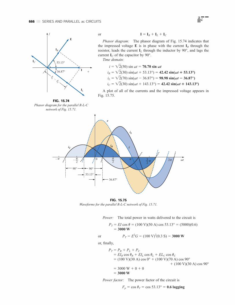
666 SERIES AND PARALLEL ac CIRCUITSa c
90°
36.87°
iL
0
e
p2
–p2
i
53.13°
90°
iR
p–
iC
tv2ppp
23
FIG. 15.75Waveforms for the parallel R-L-C network of Fig. 15.71.
or I 5 IR 1 IL 1 IC
Phasor diagram: The phasor diagram of Fig. 15.74 indicates that
the impressed voltage E is in phase with the current IR through the
resistor, leads the current IL through the inductor by 90°, and lags the
current IC of the capacitor by 90°.
Time domain:
i 5 Ï2w(50) sin qt 5 70.70 sin qt
iR 5 Ï2w(30) sin(qt 1 53.13°) 5 42.42 sin(qt 1 53.13°)
iL 5 Ï2w(70) sin(qt 2 36.87°) 5 98.98 sin(qt 2 36.87°)
iC 5 Ï2w(30) sin(qt 1 143.13°) 5 42.42 sin(qt 1 143.13°)
A plot of all of the currents and the impressed voltage appears in
Fig. 15.75.
36.87°
53.13°
j
+
IC
I
IR
E
IL – I
C
IL
FIG. 15.74Phasor diagram for the parallel R-L-C
network of Fig. 15.71.
Power: The total power in watts delivered to the circuit is
PT 5 EI cos v 5 (100 V)(50 A) cos 53.13° 5 (5000)(0.6)
5 3000 W
or PT 5 E2G 5 (100 V)2(0.3 S) 5 3000 W
or, finally,
PT 5 PR 1 PL 1 PC
5 EIR cos vR 1 EIL cos vL 1 ELC cos vC
5 (100 V)(30 A) cos 0° 1 (100 V)(70 A) cos 90°
1 (100 V)(30 A) cos 90°
5 3000 W 1 0 1 0
5 3000 W
Power factor: The power factor of the circuit is
Fp 5 cos vT 5 cos 53.13° 5 0.6 lagging
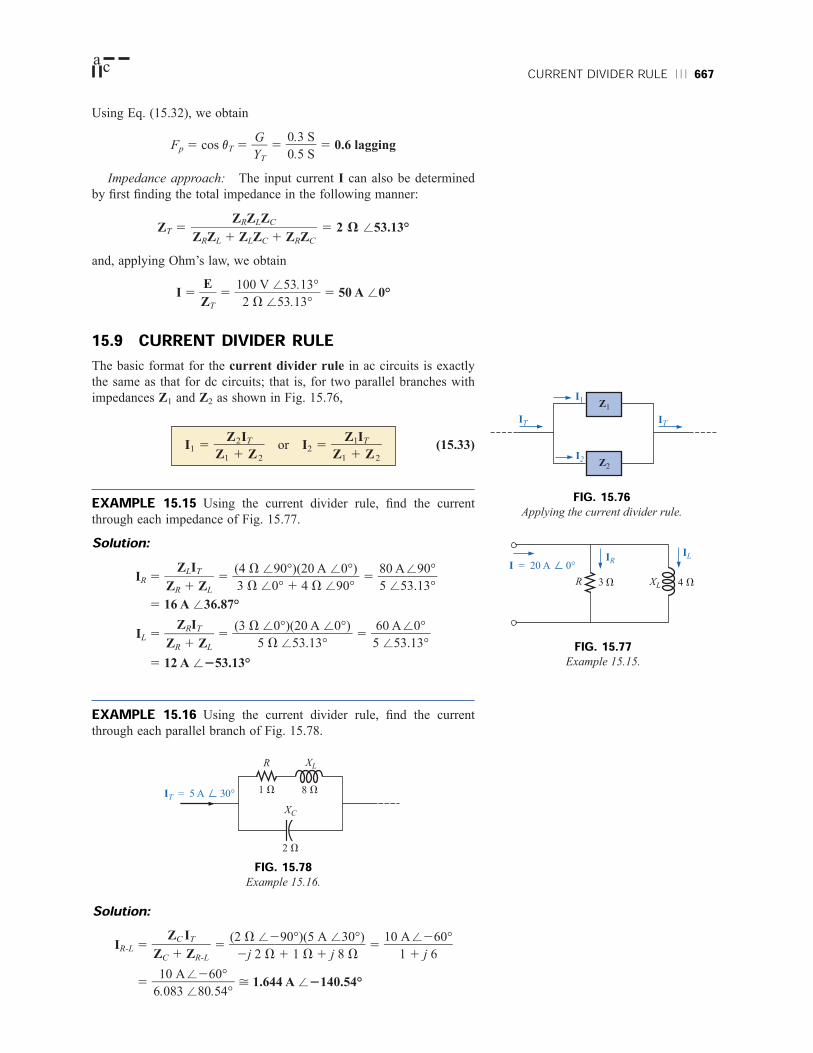
CURRENT DIVIDER RULE 667a c
IT = 5 A 30°
R
1 V
XL
8 V
XC
2 V
XL 4 VV
I = 20 A 0°IL
R 3
IR
Using Eq. (15.32), we obtain
Fp 5 cos vT 5 5 5 0.6 lagging
Impedance approach: The input current I can also be determined
by first finding the total impedance in the following manner:
ZT 5 5 2 V /53.13°
and, applying Ohm’s law, we obtain
I 5 Z
E
T
5 5 50 A /0°
15.9 CURRENT DIVIDER RULEThe basic format for the current divider rule in ac circuits is exactly
the same as that for dc circuits; that is, for two parallel branches with
impedances Z1 and Z2 as shown in Fig. 15.76,
(15.33)
EXAMPLE 15.15 Using the current divider rule, find the current
through each impedance of Fig. 15.77.
Solution:IR 5 5 5
5 16 A /36.87°
IL 5 5 5
5 12 A /253.13°
EXAMPLE 15.16 Using the current divider rule, find the current
through each parallel branch of Fig. 15.78.
60 A/0°5 /53.13°
(3 V /0°)(20 A /0°)
5 V /53.13°
ZRITZR 1 ZL
80 A/90°5 /53.13°
(4 V /90°)(20 A /0°)3 V /0° 1 4 V /90°
ZLITZR 1 ZL
I1 5 Z1
Z
12IT
Z2
or I2 5 Z1
Z
11IT
Z2
100 V /53.13°
2 V /53.13°
ZRZLZCZRZL 1 ZLZC 1 ZRZC
0.3 S0.5 S
GYT
Solution:IR-L 5 5 5
5 > 1.644 A /2140.54°10 A/260°6.083 /80.54°
10 A/260°
1 1 j 6
(2 V /290°)(5 A /30°)
2j 2 V 1 1 V 1 j 8 V
ZC ITZC 1 ZR-L
IT
Z1
Z2
IT
I1
I2
FIG. 15.76Applying the current divider rule.
FIG. 15.77Example 15.15.
FIG. 15.78Example 15.16.

668 SERIES AND PARALLEL ac CIRCUITSa c
IC 5 5
5 5
5 6.625 A /32.33°
15.10 FREQUENCY RESPONSE OF THEPARALLEL R-L NETWORKIn Section 15.5 the frequency response of a series R-C circuit was ana-
lyzed. Let us now note the impact of frequency on the total impedance
and inductive current for the parallel R-L network of Fig. 15.79 for a
frequency range of zero through 40 kHz.
40.30 A/112.87°
6.083 /80.54°
(8.06 /82.87°)(5 A/30°)
6.08 /80.54°
(1 V 1 j 8 V)(5 A /30°)
6.08 V /80.54°
ZR-LITZR-L 1 ZC
ZT Before getting into specifics, let us first develop a “sense” for the
impact of frequency on the network of Fig. 15.79 by noting the imped-
ance-versus-frequency curves of the individual elements, as shown in
Fig. 15.80. The fact that the elements are now in parallel requires that
we consider their characteristics in a different manner than occurred for
the series R-C circuit of Section 15.5. Recall that for parallel elements,
the element with the smallest impedance will have the greatest impact
R 220 V L 4 mHVs
+
–
ZTIL
I = 100 mA ∠0°
f : 0 to 20 kHz
FIG. 15.79Determining the frequency response of a parallel R-L network.
R 220 V LL = 4 mH
ZT
R
220 V
0 f
XL
0 ff2
220 Ω
XL < R XL > R
XL = 2 fLp
FIG. 15.80The frequency response of the individual elements of a parallel R-L network.

FREQUENCY RESPONSE OF THE PARALLEL R-L NETWORK 669a c
on the total impedance at that frequency. In Fig. 15.80, for example, XL
is very small at low frequencies compared to R, establishing XL as the
predominant factor in this frequency range. In other words, at low fre-
quencies the network will be primarily inductive, and the angle associ-
ated with the total impedance will be close to 90°, as with a pure induc-
tor. As the frequency increases, XL will increase until it equals the
impedance of the resistor (220 V). The frequency at which this situation
occurs can be determined in the following manner:
XL 5 2pf2L 5 R
and (15.34)
which for the network of Fig. 15.79 is
f 2 5 5
ù 8.75 kHz
which falls within the frequency range of interest.
For frequencies less than f2, XL < R, and for frequencies greater than
f2, XL > R, as shown in Fig. 15.80. A general equation for the total
impedance in vector form can be developed in the following manner:
ZT 5
5 5
and ZT 5 /90° 2tan21 XL /R
so that (15.35)
and (15.36)
The magnitude and angle of the total impedance can now be found
at any frequency of interest simply by substituting Eqs. (15.35) and
(15.36).
f 5 1 kHzXL 5 2pf L 5 2p(1 kHz)(4 3 1023 H) 5 25.12 V
and
ZT 5 5 5 24.96 V
with vT 5 tan21 5 tan21
5 tan21 8.76 5 83.49°
220 V25.12 V
RXL
(220 V)(25.12 V)Ï(2w2w0w Vw)2w 1w (w2w5w.1w2w Vw)2w
RXLÏRw2w1w Xw2
Lw
vT 5 90° 2 tan21 X
R
L 5 tan21
X
R
L
ZT 5 ÏRw
R
2
X
w1wL
Xw2Lw
RXLÏRw2w1w Xw2
Lw
RXL /90°ÏRw2w1w Xw2
Lw /tan21 XL /R
(R /0°)(XL /90°)
R 1 j XL
ZRZLZR 1 ZL
220 V2p(4 3 1023 H)
R2pL
f2 5 2p
R
L

670 SERIES AND PARALLEL ac CIRCUITSa c
and ZT 5 24.96 V /83.49°
This value compares very closely with XL 5 25.12 V /90°, which it
would be if the network were purely inductive (R 5 ∞ V). Our assump-
tion that the network is primarily inductive at low frequencies is there-
fore confirmed.
Continuing:
f 5 5 kHz: ZT 5 109.1 V /60.23°
f 5 10 kHz: ZT 5 165.5 V /41.21°
f 5 15 kHz: ZT 5 189.99 V /30.28°
f 5 20 kHz: ZT 5 201.53 V /23.65°
f 5 30 kHz: ZT 5 211.19 V /16.27°
f 5 40 kHz: ZT 5 214.91 V /12.35°
At f 5 40 kHz, note how closely the magnitude of ZT has ap-
proached the resistance level of 220 V and how the associated angle
with the total impedance is approaching zero degrees. The result is a
network with terminal characteristics that are becoming more and more
resistive as the frequency increases, which further confirms the earlier
conclusions developed by the curves of Fig. 15.80.
Plots of ZT versus frequency in Fig. 15.81 and vT in Fig. 15.82
clearly reveal the transition from an inductive network to one that
has resistive characteristics. Note that the transition frequency of
8.75 kHz occurs right in the middle of the knee of the curves for
both ZT and vT.
ZT (v)
Network inductive
XL < R (ZT ≅ XL)
100
200
R = 220 V
ZT (V)
0 1 5 10 20 30 40 f (kHz)
XL > R (ZT ≅ R)
Network resistive
XL = R
8.75
FIG. 15.81The magnitude of the input impedance versus frequency for the network of
Fig. 15.79.
A review of Figs. 15.47 and 15.81 will reveal that a series R-C and
a parallel R-L network will have an impedance level that approaches
the resistance of the network at high frequencies. The capacitive cir-
cuit approaches the level from above, whereas the inductive network
does the same from below. For the series R-L circuit and the parallel
R-C network, the total impedance will begin at the resistance level and
then display the characteristics of the reactive elements at high fre-
quencies.

FREQUENCY RESPONSE OF THE R-L NETWORK 671a c
IL Applying the current divider rule to the network of Fig. 15.79 will
result in the following:
IL 5
5 5
and IL 5 IL /vL 5 /2tan21 XL /R
The magnitude of IL is therefore determined by
(15.37)
and the phase angle vL, by which IL leads I, is given by
(15.38)
Because vL is always negative, the magnitude of vL is, in actuality,
the angle by which IL lags I.
To begin our analysis, let us first consider the case of f 5 0 Hz (dc
conditions).
f 5 0 HzXL 5 2pfL 5 2p(0 Hz)L 5 0 V
Applying the short-circuit equivalent for the inductor in Fig. 15.79
would result in
IL 5 I 5 100 mA /0°
vL 5 2tan21 X
R
L
IL 5 ÏRw
R
2wI
1w Xw2Lw
RIÏRw2w1w Xw2
Lw
RI /0°ÏRw2w1w Xw2
Lw /tan21 XL /R
(R /0°)(I /0°)
R 1 j XL
ZRIZR 1 ZL
5 f (kHz)1 10 20 30 40
0°
30°
45°
60°
90°
Inductive (XL < R)
Resistive (XL > R)
Tθ
T ( f )θ
FIG. 15.82The phase angle of the input impedance versus frequency for the network of
Fig. 15.79.

672 SERIES AND PARALLEL ac CIRCUITSa c
as appearing in Figs. 15.83 and 15.84.
f 5 1 kHz Applying Eq. (15.37):
XL 5 2pfL 5 2p(1 kHz)(4 mH) 5 25.12 V
and ÏRw2w1w Xw2Lw 5 Ï(2w2w0w Vw)2w 1w (w2w5w.1w2w Vw)2w 5 221.43 V
and IL 5 5 5 99.35 mA
with
vL 5 tan21 5 2tan21 5 2tan21 0.114 5 26.51°
and IL 5 99.35 mA /26.51°
The result is a current IL that is still very close to the source current I
in both magnitude and phase.
Continuing:
f 5 5 kHz: IL 5 86.84 mA /229.72°f 5 10 kHz: IL 5 65.88 mA /248.79°f 5 15 kHz: IL 5 50.43 mA /259.72°f 5 20 kHz: IL 5 40.11 mA /266.35°f 5 30 kHz: IL 5 28.02 mA /273.73°f 5 40 kHz: IL 5 21.38 mA /277.65°
The plot of the magnitude of IL versus frequency is provided in Fig.
15.83 and reveals that the current through the coil dropped from its
maximum of 100 mA to almost 20 mA at 40 kHz. As the reactance of
the coil increased with frequency, more of the source current chose the
25.12 V220 V
XLR
(220 V)(100 mA)
221.43 V
RIÏRw2w1w Xw2
Lw
FIG. 15.83The magnitude of the current IL versus frequency for the parallel R-L network
of Fig. 15.79.
IL (mA)
5 f (kHz)1 10 20 30 400
25
Network inductive
IL ( f )
50
75
100
XL < R (IL ≅ Is)
Network resistive
XL > R (IL => 0 mA)

SUMMARY: PARALLEL ac NETWORKS 673a c
FIG. 15.84The phase angle of the current IL versus frequency for the parallel R-L network
of Fig. 15.79.
Network inductive
5 10 20 30 40 f (kHz)0°
–30°
–45°
–60°
–90°
Network resistive
L ( f )θ
L of ILθ
L = sθ θ
R ≅ s ≅ 0°θ θ
83.49°
Vs
IR
IL
I
–6.51°
12.35° VsIR
I–77.65°IL
FIG. 15.85The phasor diagram for the parallel R-L net-
work of Fig. 15.79 at f 5 1 kHz.
FIG. 15.86The phasor diagram for the parallel R-L net-
work of Fig. 15.79 at f 5 40 kHz.
lower-resistance path of the resistor. The magnitude of the phase angle
between IL and I is approaching 90° with an increase in frequency, as
shown in Fig. 15.84, leaving its initial value of zero degrees at f 5 0 Hz
far behind.
At f 5 1 kHz, the phasor diagram of the network appears as shown
in Fig. 15.85. First note that the magnitude and the phase angle of IL are
very close to those of I. Since the voltage across a coil must lead the
current through a coil by 90°, the voltage Vs appears as shown. The
voltage across a resistor is in phase with the current through the resis-
tor, resulting in the direction of IR shown in Fig. 15.85. Of course, at
this frequency R > XL, and the current IR is relatively small in magni-
tude.
At f 5 40 kHz, the phasor diagram changes to that appearing in Fig.
15.86. Note that now IR and I are close in magnitude and phase because
XL > R. The magnitude of IL has dropped to very low levels, and the
phase angle associated with IL is approaching 290°. The network is
now more “resistive” compared to its “inductive” characteristics at low
frequencies.
The analysis of a parallel R-C or R-L-C network would proceed in
much the same manner, with the inductive impedance predominating at
low frequencies and the capacitive reactance predominating at high fre-
quencies.
15.11 SUMMARY: PARALLEL ac NETWORKSThe following is a review of important conclusions that can be derived
from the discussion and examples of the previous sections. The list is
not all-inclusive, but it does emphasize some of the conclusions that
should be carried forward in the future analysis of ac systems.

674 SERIES AND PARALLEL ac CIRCUITSa c
For parallel ac networks with reactive elements:
1. The total admittance (impedance) will be frequency
dependent.
2. The impedance of any one element can be less than the total
impedance (recall that for dc circuits the total resistance must
always be less than the smallest parallel resistor).
3. The inductive and capacitive susceptances are in direct
opposition on an admittance diagram.
4. Depending on the frequency applied, the same network can be
either predominantly inductive or predominantly capacitive.
5. At lower frequencies the inductive elements will usually have
the most impact on the total impedance, while at high
frequencies the capacitive elements will usually have the most
impact.
6. The magnitude of the current through any one branch can be
greater than the source current.
7. The magnitude of the current through an element, compared
to the other elements of the network, is directly related to the
magnitude of its impedance; that is, the smaller the impedance
of an element, the larger the magnitude of the current through
the element.
8. The current through a coil is always in direct opposition with
the current through a capacitor on a phasor diagram.
9. The applied voltage is always in phase with the current
through the resistive elements, leads the voltage across all the
inductive elements by 90°, and lags the current through all
capacitive elements by 90°.
10. The smaller the resistive element of a network compared to the
net reactive susceptance, the closer the power factor is to
unity.
15.12 EQUIVALENT CIRCUITSIn a series ac circuit, the total impedance of two or more elements in
series is often equivalent to an impedance that can be achieved with
fewer elements of different values, the elements and their values being
determined by the frequency applied. This is also true for parallel cir-
cuits. For the circuit of Fig. 15.87(a),
ZT 5 5 5
5 10 V /290°
50 /0°5 /90°
(5 V /290°)(10 V /90°)5 V /290° 1 10 V /90°
ZCZLZC 1 ZL
5 VXCZT 10 VXL
(a)
10 VXCZT
(b)
FIG. 15.87Defining the equivalence between two networks at a specific frequency.

EQUIVALENT CIRCUITS 675a c
Rs
Zs = Zp
Ys = Yp
Xs
(b)
(a)
RpZp
Yp
XP
The total impedance at the frequency applied is equivalent to a capaci-
tor with a reactance of 10 V, as shown in Fig. 15.87(b). Always keep in
mind that this equivalence is true only at the applied frequency. If the
frequency changes, the reactance of each element changes, and the
equivalent circuit will change—perhaps from capacitive to inductive in
the above example.
Another interesting development appears if the impedance of a par-
allel circuit, such as the one of Fig. 15.88(a), is found in rectangular
form. In this case,
ZT 5 5
5 5 2.40 V /36.87°
5 1.920 V 1 j 1.440 V
which is the impedance of a series circuit with a resistor of 1.92 V and
an inductive reactance of 1.44 V, as shown in Fig. 15.88(b).
The current I will be the same in each circuit of Fig. 15.87 or Fig.
15.88 if the same input voltage E is applied. For a parallel circuit of one
resistive element and one reactive element, the series circuit with the
same input impedance will always be composed of one resistive and
one reactive element. The impedance of each element of the series cir-
cuit will be different from that of the parallel circuit, but the reactive
elements will always be of the same type; that is, an R-L circuit and an
R-C parallel circuit will have an equivalent R-L and R-C series circuit,
respectively. The same is true when converting from a series to a paral-
lel circuit. In the discussion to follow, keep in mind that
the term equivalent refers only to the fact that for the same applied
potential, the same impedance and input current will result.
To formulate the equivalence between the series and parallel circuits,
the equivalent series circuit for a resistor and reactance in parallel can
be found by determining the total impedance of the circuit in rectangu-
lar form; that is, for the circuit of Fig. 15.89(a),
Yp 5 1 5 7 j
and
Zp 5 5
5 6 j
Multiplying the numerator and denominator of each term by R2pX
2p
results in
Zp 5 6 j
5 Rs 6 j Xs [Fig. 15.89(b)]
and (15.39)Rs 5 X
R2p
p
1
X
R
2p
2p
R2pXp
X2
p 1 R2p
RpX2p
X2
p 1 R2p
1/Xp(1/Rp)
2 1 (1/Xp)2
1/Rp(1/Rp)
2 1 (1/Xp)2
1(1/Rp) 7 j (1/Xp)
1Yp
1Xp
1RP
16j Xp
1Rp
12 /90°5 /53.13°
(4 V /90°)(3 V /0°)4 V /90° 1 3 V /0°
ZLZRZL 1 ZR
4 V R 3 VXL
I
ZT
E
+
–
(a)
XL = 1.44 VI
ZT
E
+
–
(b)
R = 1.92 V
FIG. 15.88Finding the series equivalent circuit
for a parallel R-L network.
FIG. 15.89Defining the parameters of equivalent series
and parallel networks.

676 SERIES AND PARALLEL ac CIRCUITSa c
with (15.40)
For the network of Fig. 15.88,
Rs 5 5 5 5 1.920 V
and
Xs 5 5 5 5 1.440 V
which agrees with the previous result.
The equivalent parallel circuit for a circuit with a resistor and reac-
tance in series can be found by simply finding the total admittance of
the system in rectangular form; that is, for the circuit of Fig. 15.89(b),
Zs 5 Rs 6 j Xs
Ys 5 5 5 7 j
5 Gp 7 j Bp 5 7 j [Fig. 15.89(a)]
or (15.41)
with (15.42)
For the above example,
Rp 5 5 5 5 3.0 V
and Xp 5 5 5 4.0 V
as shown in Fig. 15.88(a).
EXAMPLE 15.17 Determine the series equivalent circuit for the net-
work of Fig. 15.90.
5.76 V
1.44
R2s 1 X2
s
Xs
5.76 V
1.92
(1.92 V)2 1 (1.44 V)2
1.92 V
R2s 1 X2
s
Rs
Xp 5 R2
s
X
1
s
X2s
Rp 5 R2
s
R
1
s
X2s
1Xp
1Rp
XsR2
s 1 X2s
RsR2
s 1 X2s
1Rs 6 j Xs
1Zs
36 V
25
(3 V)2(4 V)(4 V)2 1 (3 V)2
R2p Xp
X2
p 1 R2p
48 V
25
(3 V)(4 V)2
(4 V)2 1 (3 V)2
RpX2p
X2
p 1 R2p
Xs 5 X2
p
R
1
2pX
R
p
2p
4 kV
R 8 kV
XC
9 kVXL
Rp
Xp
FIG. 15.90Example 15.17.

EQUIVALENT CIRCUITS 677a c
Solution:Rp 5 8 kV
Xp (resultant) 5 XL 2 XC 5 9 kV 2 4 kV5 5 kV
and
Rs 5 5 5 5 2.247 kV
with
Xs 5 5 5
5 3.596 kV (inductive)
The equivalent series circuit appears in Fig. 15.91.
EXAMPLE 15.18 For the network of Fig. 15.92:
320 kV
89
(8 kV)2(5 kV)(5 kV)2 1 (8 kV)2
R2p Xp
X2
p 1 R2p
200 kV
89
(8 kV)(5 kV)2
(5 kV)2 1 (8 kV)2
RpX2p
X2
p 1 R2p
3.596 kV2.247 kV
XsRs
FIG. 15.91The equivalent series circuit for the parallel
network of Fig. 15.90.
R1 10 V R2 40 V L1 6 mH L2 12 mHC1
80 mFC2
20 mF
iL
i = =2 (12) sin 1000t
+
YT
ei
–
ZT
FIG. 15.92Example 15.18.
a. Determine YT.
b. Sketch the admittance diagram.
c. Find E and IL.
d. Compute the power factor of the network and the power delivered to
the network.
e. Determine the equivalent series circuit as far as the terminal charac-
teristics of the network are concerned.
f. Using the equivalent circuit developed in part (e), calculate E, and
compare it with the result of part (c).
g. Determine the power delivered to the network, and compare it with
the solution of part (d).
h. Determine the equivalent parallel network from the equivalent series
circuit, and calculate the total admittance YT. Compare the result
with the solution of part (a).
Solutions:a. Combining common elements and finding the reactance of the
inductor and capacitor, we obtain
RT 5 10 V \ 40 V 5 8 V
LT 5 6 mH \ 12 mH 5 4 mH
CT 5 80 mF 1 20 mF 5 100 mF

678 SERIES AND PARALLEL ac CIRCUITSa c
XL 5 qL 5 (1000 rad/s)(4 mH) 5 4 V
XC 5 5 5 10 V
The network is redrawn in Fig. 15.93 with phasor notation. The total
admittance is
YT 5 YR 1 YL 1 YC
5 G /0° 1 BL /290° 1 BC /190°
5 /0° 1 /290° 1 /190°
5 0.125 S /0° 1 0.25 S /290° 1 0.1 S /190°
5 0.125 S 2 j 0.25 S 1 j 0.1 S
5 0.125 S 2 j 0.15 S 5 0.195 S /250.194°
110 V
14 V
18 V
1(1000 rad/s)(100 mF)
1qC
b. See Fig. 15.94.
c. E 5 IZT 5 5 5 61.538 V /50.194°
IL 5 5 5 5 15.385 A /239.81°
d. Fp 5 cos v 5 5 5 0.641 lagging (E leads I)
P 5 EI cos v 5 (61.538 V)(12 A) cos 50.194°
5 472.75 W
e. ZT 5 5 5 5.128 V /150.194°
5 3.283 V 1 j 3.939 V
5 R 1 j XL
XL 5 3.939 V 5 qL
L 5 5 5 3.939 mH
The series equivalent circuit appears in Fig. 15.95.
f. E 5 IZT 5 (12 A /0°)(5.128 V /50.194°)
5 61.536 V /50.194° (as above)
g. P 5 I2R 5 (12 A)2 (3.283 V) 5 472.75 W (as above)
h. Rp 5 5 5 8 V(3.283 V)2 1 (3.939 V)2
3.283 V
R2s 1 X2
s
Rs
3.939 V1000 rad/s
3.939 V
q
10.195 S /250.194°
1YT
0.125 S0.195 S
GYT
61.538 V /50.194°
4 V /90°
EZL
VLZL
12 A /0°0.195 S /250.194°
IYT
R 8 V 4 VXL XC10 V
YT
IL
+
–
EI = 12 A ∠ 0°
FIG. 15.93Applying phasor notation to the network of Fig. 15.92.
G ∠ 0°
–50.194°
0.195 S
YT
BL ∠ –90°
BL – BC
BC ∠ 90°
j
+–
FIG. 15.94Admittance diagram for the parallel R-L-C
network of Fig. 15.92.
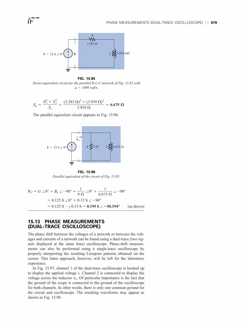
PHASE MEASUREMENTS (DUAL-TRACE OSCILLOSCOPE) 679a c
Xp 5 5 5 6.675 V
The parallel equivalent circuit appears in Fig. 15.96.
(3.283 V)2 1 (3.939 V)2
3.939 V
R2s 1 X2
s
Xs
YT 5 G /0° 1 BL /290° 5 /0° 1 /290°
5 0.125 S /0° 1 0.15 S /290°
5 0.125 S 2 j 0.15 S 5 0.195 S /250.194° (as above)
15.13 PHASE MEASUREMENTS(DUAL-TRACE OSCILLOSCOPE)The phase shift between the voltages of a network or between the volt-
ages and currents of a network can be found using a dual-trace (two sig-
nals displayed at the same time) oscilloscope. Phase-shift measure-
ments can also be performed using a single-trace oscilloscope by
properly interpreting the resulting Lissajous patterns obtained on the
screen. This latter approach, however, will be left for the laboratory
experience.
In Fig. 15.97, channel 1 of the dual-trace oscilloscope is hooked up
to display the applied voltage e. Channel 2 is connected to display the
voltage across the inductor vL. Of particular importance is the fact that
the ground of the scope is connected to the ground of the oscilloscope
for both channels. In other words, there is only one common ground for
the circuit and oscilloscope. The resulting waveforms may appear as
shown in Fig. 15.98.
16.675 V
18 V
FIG. 15.95Series equivalent circuit for the parallel R-L-C network of Fig. 15.92 with
q 5 1000 rad/s.
L
R
3.283 V
3.939 mHE
+
–
I = 12 A ∠ 0°
LR 8 V 6.675 VI = 12 A ∠ 0°
YT
FIG. 15.96Parallel equivalent of the circuit of Fig. 15.95.

680 SERIES AND PARALLEL ac CIRCUITSa c
R
Le
+
–
vL
+
–
21
Oscilloscope
FIG. 15.97Determining the phase relationship between e and vL.
v
θ1.6 div.
e
T = 8 div.
FIG. 15.98Determining the phase angle between e and vL.
For the chosen horizontal sensitivity, each waveform of Fig. 15.98
has a period T defined by eight horizontal divisions, and the phase angle
between the two waveforms is defined by 11
2 divisions. Using the fact
that each period of a sinusoidal waveform encompasses 360°, the fol-
lowing ratios can be set up to determine the phase angle v:
8
36
d
0
iv
°
. 5
1.6
v
div.
and v 5 1 2360° 5 72°
In general,
(15.43)
If the phase relationship between e and vR is required, the oscillo-
scope must not be hooked up as shown in Fig. 15.99. Points a and b
have a common ground that will establish a zero-volt drop between the
two points; this drop will have the same effect as a short-circuit con-
nection between a and b. The resulting short circuit will “short out” the
inductive element, and the current will increase due to the drop in
impedance for the circuit. A dangerous situation can arise if the induc-
tive element has a high impedance and the resistor has a relatively low
v 5 (
(
d
d
i
i
v
v
.
.
f
f
o
o
r
r
T
v)
) 3 360°
1.68
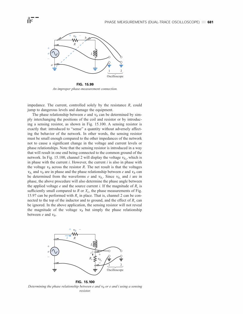
PHASE MEASUREMENTS (DUAL-TRACE OSCILLOSCOPE) 681a c
impedance. The current, controlled solely by the resistance R, could
jump to dangerous levels and damage the equipment.
The phase relationship between e and vR can be determined by sim-
ply interchanging the positions of the coil and resistor or by introduc-
ing a sensing resistor, as shown in Fig. 15.100. A sensing resistor is
exactly that: introduced to “sense” a quantity without adversely affect-
ing the behavior of the network. In other words, the sensing resistor
must be small enough compared to the other impedances of the network
not to cause a significant change in the voltage and current levels or
phase relationships. Note that the sensing resistor is introduced in a way
that will result in one end being connected to the common ground of the
network. In Fig. 15.100, channel 2 will display the voltage vRs, which is
in phase with the current i. However, the current i is also in phase with
the voltage vR across the resistor R. The net result is that the voltages
vRsand vR are in phase and the phase relationship between e and vR can
be determined from the waveforms e and vRs. Since vRs
and i are in
phase, the above procedure will also determine the phase angle between
the applied voltage e and the source current i. If the magnitude of Rs is
sufficiently small compared to R or XL, the phase measurements of Fig.
15.97 can be performed with Rs in place. That is, channel 2 can be con-
nected to the top of the inductor and to ground, and the effect of Rs can
be ignored. In the above application, the sensing resistor will not reveal
the magnitude of the voltage vR but simply the phase relationship
between e and vR.
R
Le
+
–
21
vR–+
Oscilloscope
a
b
FIG. 15.99An improper phase-measurement connection.
R
L
e
+
–
21
vR–+
vRs
+
–
Rs
i
i
Oscilloscope
FIG. 15.100Determining the phase relationship between e and vR or e and i using a sensing
resistor.

682 SERIES AND PARALLEL ac CIRCUITSa c
For the parallel network of Fig. 15.101, the phase relationship
between two of the branch currents, iR and iL, can be determined using
a sensing resistor, as shown in the figure. Channel 1 will display the
voltage vR, and channel 2 will display the voltage vRs. Since vR is in
phase with iR, and vRsis in phase with the current iL, the phase rela-
tionship between vR and vRswill be the same as that between iR and iL.
In this case, the magnitudes of the current levels can be determined
using Ohm’s law and the resistance levels R and Rs, respectively.
FIG. 15.101Determining the phase relationship between iR and iL.
L
e
+
–
21
iRiL
vRsRs
+
–
vR
+
–R C
Oscilloscope
e
+
–
2
1
is
vRs+–
R
isRs
FIG. 15.102Determining the phase relationship between e
and is.
If the phase relationship between e and is of Fig. 15.101 is required,
a sensing resistor can be employed, as shown in Fig. 15.102.
In general, therefore, for dual-trace measurements of phase relation-
ships, be particularly careful of the grounding arrangement, and fully
utilize the in-phase relationship between the voltage and current of a
resistor.
15.14 APPLICATIONSHome WiringAn expanded view of house wiring is provided in Fig. 15.103 to permit
a discussion of the entire system. The house panel has been included
with the “feed” and the important grounding mechanism. In addition, a

APPLICATIONS 683a c
number of typical circuits found in the home have been included to pro-
vide a sense for the manner in which the total power is distributed.
First note how the copper bars in the panel are laid out to provide
both 120 V and 208 V. Between any one bar and ground is the single-
phase 120-V supply. However, the bars have been arranged so that
208 V can be obtained between two vertical adjacent bars using a
double-gang circuit breaker. When time permits, examine your own
panel (but do not remove the cover), and note the dual circuit breaker
arrangement for the 208-V supply.
For appliances such as fixtures and heaters that have a metal casing,
the ground wire is connected to the metal casing to provide a direct path
to ground path for a “shorting” or errant current as described in Section
7.7. For outlets and such that do not have a conductive casing, the
ground lead is connected to a point on the outlet that distributes to all
important points of the outlet.
Note the series arrangement between the thermostat and the heater
but the parallel arrangement between heaters on the same circuit. In
addition, note the series connection of switches to lights in the upper-
right corner but the parallel connection of lights and outlets. Due to
high current demand the air conditioner, heaters, and electric stove have
30-A breakers. Keep in mind that the total current does not equal the
product of the two (or 60 A) since each breaker is in a line and the same
current will flow through each breaker.
In general, you now have a surface understanding of the general
wiring in your home. You may not be a qualified, licensed electrician,
Neutral Line 1 Line 2
Mainbreaker200 A Copper bus-bars
Lighting Series switches20 A
40 A
40 A
30 A
30 A
15 A
15 A
30 A
30 A
30 A
30 A
#14
#14
#10
#10
#10
#10
Parallellamps
120 V
+
–
120 V+
–
Washingmachine
400 W
Electric dryer
4.8 kW
208 V+
–
208 V+
–Thermostat
2′ section 4′ section 8′ section
2300 W
Parallel electricbaseboard heaters
Neutral bus-bar
Ground bus bar
MAIN PANEL
#12
#8
#8
#10
#10
Switched outlets Parallel outlets
12.2-kWelectric range
Air conditioner
860 W
208 V+
–
208 V+
–
120V
+
–60 W 40 W 60 W60 W
575 W 1150 W
FIG. 15.103Home wiring diagram.
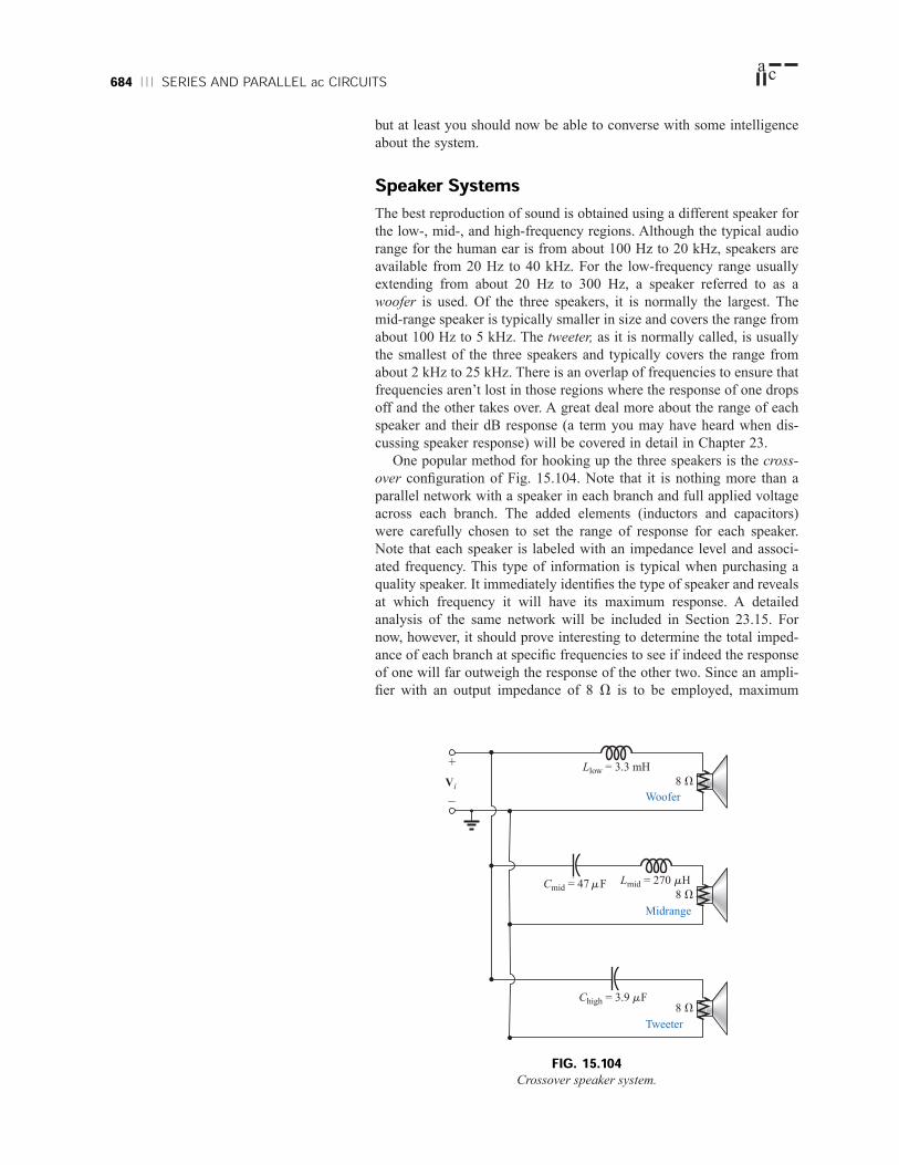
684 SERIES AND PARALLEL ac CIRCUITSa c
but at least you should now be able to converse with some intelligence
about the system.
Speaker SystemsThe best reproduction of sound is obtained using a different speaker for
the low-, mid-, and high-frequency regions. Although the typical audio
range for the human ear is from about 100 Hz to 20 kHz, speakers are
available from 20 Hz to 40 kHz. For the low-frequency range usually
extending from about 20 Hz to 300 Hz, a speaker referred to as a
woofer is used. Of the three speakers, it is normally the largest. The
mid-range speaker is typically smaller in size and covers the range from
about 100 Hz to 5 kHz. The tweeter, as it is normally called, is usually
the smallest of the three speakers and typically covers the range from
about 2 kHz to 25 kHz. There is an overlap of frequencies to ensure that
frequencies aren’t lost in those regions where the response of one drops
off and the other takes over. A great deal more about the range of each
speaker and their dB response (a term you may have heard when dis-
cussing speaker response) will be covered in detail in Chapter 23.
One popular method for hooking up the three speakers is the cross-
over configuration of Fig. 15.104. Note that it is nothing more than a
parallel network with a speaker in each branch and full applied voltage
across each branch. The added elements (inductors and capacitors)
were carefully chosen to set the range of response for each speaker.
Note that each speaker is labeled with an impedance level and associ-
ated frequency. This type of information is typical when purchasing a
quality speaker. It immediately identifies the type of speaker and reveals
at which frequency it will have its maximum response. A detailed
analysis of the same network will be included in Section 23.15. For
now, however, it should prove interesting to determine the total imped-
ance of each branch at specific frequencies to see if indeed the response
of one will far outweigh the response of the other two. Since an ampli-
fier with an output impedance of 8 V is to be employed, maximum
8 V
Llow = 3.3 mH
Vi
+
–
8 V
8 V
Cmid = 47 Fm Lmid = 270 Hm
Chigh = 3.9 Fm
Woofer
Tweeter
Midrange
FIG. 15.104Crossover speaker system.

APPLICATIONS 685a c
transfer of power (see Section 18.5 for ac networks) to the speaker will
result when the impedance of the branch is equal to or very close to 8 V.
Let us begin by examining the response of the frequencies to be car-
ried primarily by the mid-range speaker since it represents the greatest
portion of the human hearing range. Since the mid-range speaker
branch is rated at 8 V at 1.4 kHz, let us test the effect of applying 1.4 kHz
to all branches of the crossover network.
For the mid-range speaker:
XC 5 2p
1
fC 5 5 2.42 V
XL 5 2pfL 5 2p(1.4 kHz)(270 mH) 5 2.78 V
R 5 8 V
and Zmid-range 5 R 1 j (XL 2 XC) 5 8 V 1 j (2.78 V 2 2.42 V)
5 8 V 1 j 0.36 V
5 8.008 V /22.58° > 8 V /0° 5 R
In Fig. 15.105(a), the amplifier with the output impedance of 8 V
has been applied across the mid-range speaker at a frequency of
1.4 kHz. Since the total reactance offered by the two series reactive ele-
ments is so small compared to the 8-V resistance of the speaker, we can
essentially replace the series combination of the coil and capacitor by a
short circuit of 0 V. We are then left with a situation where the load
impedance is an exact match with the output impedance of the ampli-
fier, and maximum power will be delivered to the speaker. Because of
the equal series impedances, each will capture half the applied voltage
or 6 V. The power to the speaker is then V2/R 5 (6 V)2/8 V 5 4.5 W.
At a frequency of 1.4 kHz we would expect the woofer and tweeter
to have minimum impact on the generated sound. We will now test the
validity of this statement by determining the impedance of each branch
at 1.4 kHz.
For the woofer:
XL 5 2pfL 5 2p(1.4 kHz)(3.3 mH) 5 29.03 V
and Zwoofer 5 R 1 j XL 5 8 V 1 j 29.03 V
5 30.11 V /74.59°
which is a poor match with the output impedance of the amplifier. The
resulting network is shown in Fig. 15.105(b).
The total load on the source of 12 V is
ZT 5 8 V 1 8 V 1 j 29.03 V 5 16 V 1 j 29.03 V
5 33.15 V /61.14°
and the current is
I 5 5
5 362 mA /261.14°
The power to the 8-V speaker is then
Pwoofer 5 I2R 5 (362 mA)28 V 5 1.048 W
or about 1 W.
Consequently, the sound generated by the mid-range speaker will far
outweigh the response of the woofer (as it should).
12 V /0°33.15 V /61.14°
EZT
12p(1.4 kHz)(47 mF)

686 SERIES AND PARALLEL ac CIRCUITSa c
For the tweeter:
XC 5 5 5 29.15 V
and Ztweeter 5 R 2 j XC 5 8 V 2 j 29.15 V
5 30.23 V /274.65°
which, as for the woofer, is a poor match with the output impedance of
the amplifier. The current
I 5 5
5 397 mA /74.65°
The power to the 8-V speaker is then
Ptweeter 5 I2R 5 (397 mA)2(8 V) 5 1.261 W
or about 1.3 W.
12 V /0°30.23 V /274.65°
EZT
12p(1.4 kHz)(3.9 mF)
12pfC
8 V
8 V2.42 V 2.38 V
Midrange
XL
+
–
Vspeaker
= 6 V
Amplifier
+
–
12 V
(a)
(–jXC + jXL = –j 0.04 V)
XC
8 V
8 V29.03 V
Woofer
XL
Ispeaker
= 362 mA
Amplifier
+
–
12 V
(b)
8 V
8 V29.15 V
Tweeter
Amplifier
+
–
12 V
(c)
XC
ZT
Zwoofer
Ztweeter
Ispeaker
= 397 mA
ZT
Zmidrange
FIG. 15.105Crossover network: (a) mid-range speaker at 1.4 kHz; (b) woofer at 1.4 kHz;
(c) tweeter.

APPLICATIONS 687a c
Consequently, the sound generated by the mid-range speaker will far
outweigh the response of the tweeter also.
All in all, the mid-range speaker predominates at a frequency of
1.4 kHz for the crossover network of Fig. 15.104.
Just for interest sake, let us now determine the impedance of the
tweeter at 20 kHz and the impact of the woofer at this frequency.
For the tweeter:
XC 5 5 5 2.04 V
with Ztweeter 5 8 V 2 j 2.04 V 5 8.26 V /214.31°
Even though the magnitude of the impedance of the branch is not
exactly 8 V, it is very close, and the speaker will receive a high level of
power (actually 4.43 W).
For the woofer:
XL 5 2pf L 5 2p(20 kHz)(3.3 mH) 5 414.69 V
with Zwoofer 5 8 V 2 j 414.69 V 5 414.77 V /88.9°
which is a terrible match with the output impedance of the amplifier.
Therefore, the speaker will receive a very low level of power (6.69 mW >0.007 W).
For all the calculations, note that the capacitive elements predomi-
nate at low frequencies, and the inductive elements at high frequen-
cies. For the low frequencies, the reactance of the coil will be quite
small, permitting a full transfer of power to the speaker. For the high-
frequency tweeter, the reactance of the capacitor is quite small, pro-
viding a direct path for power flow to the speaker.
Phase-Shift Power ControlIn Chapter 12 the internal structure of a light dimmer was examined and
its basic operation described. We can now turn our attention to how the
power flow to the bulb is controlled.
If the dimmer were composed of simply resistive elements, all the
voltages of the network would be in phase as shown in Fig. 15.106(a).
If we assume that 20 V are required to turn on the triac of Fig. 12.49,
then the power will be distributed to the bulb for the period highlighted
by the blue area of Fig. 15.106(a). For this situation, the bulb is close to
full brightness since the applied voltage is available to the bulb for
almost the entire cycle. To reduce the power to the bulb (and therefore
reduce its brightness), the controlling voltage would have to have a
lower peak voltage as shown in Fig. 15.106(b). In fact, the waveform of
Fig. 15.106(b) is such that the turn-on voltage is not reached until the
peak value occurs. In this case power is delivered to the bulb for only
half the cycle, and the brightness of the bulb will be reduced. The prob-
lem with using only resistive elements in a dimmer now becomes
apparent: The bulb can be made no dimmer than the situation depicted
by Fig. 15.106(b). Any further reduction in the controlling voltage
would reduce its peak value below the trigger level, and the bulb would
never turn on.
This dilemma can be resolved by using a series combination of ele-
ments such as shown in Fig. 15.107(a) from the dimmer of Fig. 12.49.
Note that the controlling voltage is the voltage across the capacitor,
12p(20 kHz)(3.9 mF)
12pfC
170
20
0
V (volts)
t
Appliedvoltage
(b)
Controllingvoltage
(a)
170
20
0
V (volts)
t
Appliedvoltage
Lampvoltage
FIG. 15.106Light dimmer: (a) with purely resistive
elements; (b) half-cycle power distribution.

688 SERIES AND PARALLEL ac CIRCUITSa c
while the full line voltage of 120 V rms, 170 V peak, is across the entire
branch. To describe the behavior of the network, let us examine the case
defined by setting the potentiometer (used as a rheostat) to 1/10 its
maximum value, or 33 kV. Combining the 33 kV with the fixed resis-
tance of 47 kV will result in a total resistance of 80 kV and the equiv-
alent network of Fig. 15.107(b).
At 60 Hz, the reactance of the capacitor is
XC 5 2p
1
fC 5 5 42.78 kV
Applying the voltage divider rule:
Vcontrol 5 ZR
Z
1
CV
Z
s
C
5 5
5 0.472Vs /261.86°
Using a peak value of 170 V:
Vcontrol 5 0.472(170 V) /261.86°
5 80.24 V /261.86°
producing the waveform of Fig. 15.108(a). The result is a waveform
with a phase shift of 61.86° (lagging the applied line voltage) and a rel-
atively high peak value. The high peak value will result in a quick tran-
sition to the 20-V turn-on level, and power will be distributed to the
bulb for the major portion of the applied signal. Recall from the dis-
cussion of Chapter 12 that the response in the negative region is a
replica of that achieved in the positive region. If we reduced the poten-
tiometer resistance further, the phase angle would be reduced, and the
bulb would burn brighter. The situation is now very similar to that
described for the response of Fig. 15.106(a). In other words, nothing
has been gained thus far by using the capacitive element in the control
network. However, let us now increase the potentiometer resistance to
200 kV and note the effect on the controlling voltage.
42.78 kV Vs /290°90.72 kV /228.14°
(42.78 kV /290°)(Vs /0°)
80 kV 2 j 42.78 kV
12p(60 Hz)(62 mF)
+
–
G
K
A
TRIACDIAC
0.068 µFVcontrol
330-kVrheostat
47 kV
+
–
Vline = 170 V ∠0°(peak)
(a)
+
–
170 V ∠0°
0.068 µFC
(b)
Vcontrol
+
–
80 kVR
FIG. 15.107Light dimmer: (a) from Fig. 12.49; (b) with rheostat set at 33 kV.

COMPUTER ANALYSIS 689a c
That is,
RT 5 200 kV 1 47 kV 5 247 kV
Vcontrol 5 ZR
Z
1
CV
Z
s
C
5 5
5 0.171Vs /280.2°
and using a peak value of 170 V, we have
Vcontrol 5 0.171(170 V) /280.2°
5 29.07 V /280.2°
The peak value has been substantially reduced to only 29.07 V, and the
phase-shift angle has increased to 80.2°. The result, as depicted by Fig.
15.108(b), is that the firing potential of 20 V is not reached until near
the end of the positive region of the applied voltage. Power is delivered
to the bulb for only a very short period of time, causing the bulb to be
quite dim, significantly dimmer than obtained from the response of Fig.
15.106(b).
A conduction angle less than 90° is therefore possible due only to
the phase shift introduced by the series R-C combination. Thus, it is
possible to construct a network of some significance with a rather sim-
ple pair of elements.
15.15 COMPUTER ANALYSISPSpiceSeries R-L-C Circuit The R-L-C network of Fig. 15.35 will now be
analyzed using OrCAD Capture. Since the inductive and capacitive
42.78 kV Vs /290°250.78 kV /29.8°
(42.78 kV /290°)(Vs /0°)
247 kV 2 j 42.78 kV
170
80.24
20
0° 90° 360°61.86°
V(volts)
Vlamp
Vcontrol
Vapplied
θ
(a)
180°
170
29.0720
0° 90° 360°
80.2°
V(volts)
Vlamp
Vcontrol
Vapplied
θ
(b)
180°
FIG. 15.108Light dimmer of Fig. 12.49: (a) rheostat set at 33 kV; (b) rheostat set at 200 kV.

690 SERIES AND PARALLEL ac CIRCUITSa c
reactances cannot be entered onto the screen, the associated inductive
and capacitive levels were first determined as follows:
XL 5 2pf L ⇒ L 5 5 5 1.114 mH
XC 5 ⇒ C 5 5 5 53.05 mF
The values were then entered into the schematic as shown in Fig. 15.109.
For the ac source, the sequence is Place part icon-SOURCE-VSIN-
OK with VOFF set at 0 V, VAMPL set at 70.7 V (the peak value of
the applied sinusoidal source in Fig. 15.35), and FREQ 5 1 kHz. If we
double-click on the source symbol, the Property Editor will appear,
confirming the above choices and showing that DF 5 0 s, PHASE 5 0°,
and TD 5 0 s as set by the default levels. We are now ready to do an
analysis of the circuit for the fixed frequency of 1 kHz.
12p(1 kHz)3 V
12pf XC
12pfC
7 V2p(1 kHz)
XL2pf
FIG. 15.109Using PSpice to analyze a series R-L-C ac circuit.
The simulation process is initiated by first selecting the New Simu-
lation Profile icon and inserting SeriesRLC as the Name followed by
Create. The Simulation Settings dialog will now appear, and since we
are continuing to plot the results against time, the Time Domain(Tran-
sient) option is selected under Analysis type. Since the period of each
cycle of the applied source is 1 ms, the Run to time will be set at 5 ms
so that five cycles will appear. The Start saving data after will be left
at 0 s even though there will be an oscillatory period for the reactive
elements before the circuit settles down. The Maximum step size will
be set at 5 ms/1000 5 5 ms. Finally OK is selected followed by the

COMPUTER ANALYSIS 691a c
Run PSpice key. The result will be a blank screen with an x-axis
extending from 0 s to 5 ms.
The first quantity of interest is the current through the circuit, so
Trace-Add-Trace is selected followed by I(R) and OK. The resulting
plot of Fig. 15.110 clearly shows that there is a period of storing and
discharging of the reactive elements before a steady-state level is estab-
lished. It would appear that after 3 ms, steady-state conditions have
been essentially established. Select the Toggle cursor key, and left-
click the mouse; a cursor will result that can be moved along the axis
near the maximum value around 1.4 ms. In fact, the cursor reveals a
maximum value of 16.4 A which exceeds the steady-state solution by
over 2 A. A right click of the mouse will establish a second cursor on
the screen that can be placed near the steady-state peak around 4.4 ms.
The resulting peak value is about 14.15 A which is a match with the
longhand solution for Fig. 15.35. We will therefore assume that steady-
state conditions have been established for the circuit after 4 ms.
FIG. 15.110A plot of the current for the circuit of Fig. 15.109 showing the transition from the transient state to
the steady-state response.
Let us now add the source voltage through Trace-Add Trace-
V(Vs:+)-OK to obtain the multiple plot at the bottom of Fig. 15.111.
For the voltage across the coil, the sequence Plot-Add Plot to Window-
Trace-Add Trace-V(L:1)-V(L:2) will result in the plot appearing at
the top of Fig. 15.111. Take special note of the fact that the Trace
Expression is V(L:1)2V(L:2) rather than just V(L:1) because V(L:1)
would be the voltage from that point to ground which would include the
voltage across the capacitor. In addition, the 2 sign between the two
comes from the Functions or Macros list at right of the Add Traces
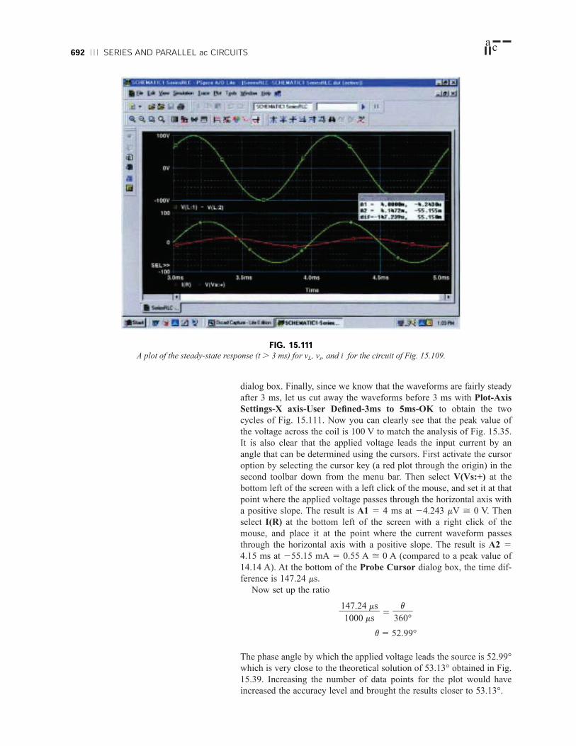
692 SERIES AND PARALLEL ac CIRCUITSa c
dialog box. Finally, since we know that the waveforms are fairly steady
after 3 ms, let us cut away the waveforms before 3 ms with Plot-Axis
Settings-X axis-User Defined-3ms to 5ms-OK to obtain the two
cycles of Fig. 15.111. Now you can clearly see that the peak value of
the voltage across the coil is 100 V to match the analysis of Fig. 15.35.
It is also clear that the applied voltage leads the input current by an
angle that can be determined using the cursors. First activate the cursor
option by selecting the cursor key (a red plot through the origin) in the
second toolbar down from the menu bar. Then select V(Vs:+) at the
bottom left of the screen with a left click of the mouse, and set it at that
point where the applied voltage passes through the horizontal axis with
a positive slope. The result is A1 5 4 ms at 24.243 mV > 0 V. Then
select I(R) at the bottom left of the screen with a right click of the
mouse, and place it at the point where the current waveform passes
through the horizontal axis with a positive slope. The result is A2 5
4.15 ms at 255.15 mA 5 0.55 A > 0 A (compared to a peak value of
14.14 A). At the bottom of the Probe Cursor dialog box, the time dif-
ference is 147.24 ms.
Now set up the ratio
5
v 5 52.99°
The phase angle by which the applied voltage leads the source is 52.99°
which is very close to the theoretical solution of 53.13° obtained in Fig.
15.39. Increasing the number of data points for the plot would have
increased the accuracy level and brought the results closer to 53.13°.
v360°
147.24 ms
1000 ms
FIG. 15.111A plot of the steady-state response (t . 3 ms) for vL, vs, and i for the circuit of Fig. 15.109.

COMPUTER ANALYSIS 693a c
Electronics WorkbenchWe will now examine the response of a network versus frequency rather
than time using the network of Fig. 15.79 which now appears on the
schematic of Fig. 15.112. The ac current source appears as AC–CUR-
RENT–SOURCE in the Sources tool bin next to the ac voltage source.
Note that the current source was given an amplitude of 1 A to establish
a magnitude match between the response of the voltage across the net-
work and the impedance of the network. That is,
) ZT ) 5 ) ) 5 ) ) 5 ) Vs )
Before applying computer methods, we should develop a rough idea
of what to expect so that we have something to which to compare the
computer solution. At very high frequencies such as 1 MHz, the imped-
ance of the inductive element will be about 25 kV which when placed
in parallel with the 220 V will look like an open circuit. The result is
that as the frequency gets very high, we should expect the impedance of
the network to approach the 220-V level of the resistor. In addition,
since the network will take on resistive characteristics at very high fre-
quencies, the angle associated with the input impedance should also
approach 0 V. At very low frequencies the reactance of the inductive
element will be much less than the 220 V of the resistor, and the net-
work will take on inductive characteristics. In fact, at, say, 10 Hz, the
reactance of the inductor is only about 0.25 V which is very close to a
short-circuit equivalent compared to the parallel 220-V resistor. The
result is that the impedance of the network is very close to 0 V at very
low frequencies. Again, since the inductive effects are so strong at low
Vs1 A
VsIs
FIG. 15.112Obtaining an impedance plot for a parallel R-L network using Electronics Workbench.

694 SERIES AND PARALLEL ac CIRCUITSa c
frequencies, the phase angle associated with the input impedance
should be very close to 90°.
Now for the computer analysis. The current source, the resistor ele-
ment, and the inductor are all placed and connected using procedures
described in detail in earlier chapters. However, there is one big differ-
ence this time that the user must be aware of: Since the output will be
plotted versus frequency, the Analysis Setup heading must be selected
in the AC Current dialog box for the current source. When selected,
the AC Magnitude must be set to the value of the ac source. In this
case, the default level of 1A matches that of the applied source, so we
were set even if we failed to check the setting. In the future, however, a
voltage or current source may be used that does not have an amplitude
of 1, and proper entries must be made to this listing.
For the simulation the sequence Simulate-Analyses-AC Analysis is
first applied to obtain the AC Analysis dialog box. The Start fre-
quency will be set at 10 Hz so that we have entries at very low fre-
quencies, and the Stop frequency will be set at 1MHz so that we have
data points at the other end of the spectrum. The Sweep type can
remain Decade, but the number of points per decade will be 1000 so
that we obtain a detailed plot. The Vertical scale will be set on Linear.
Within Output variables we find that only one node, 1, is defined.
Shifting it over to the Selected variables for analysis column using the
Plot during simulation key pad and then hitting the Simulate key will
result in the two plots of Fig. 15.112. The Show/Hide Grid key was
selected to place the grid on the graph, and the Show/Hide Cursors
key was selected to place the AC Analysis dialog box appearing in Fig.
15.112. Since two graphs are present, we must define the one we are
working on by clicking on the Voltage or Phase heading on the left side
of each plot. A small red arrow will appear when selected to keep us
aware of the active plot. When setting up the cursors, be sure that you
have activated the correct plot. When the red cursor is moved to 10 Hz
(x1), we find that the voltage across the network is only 0.251 V (y1),
resulting in an input impedance of only 0.25 V—quite small and
matching our theoretical prediction. In addition, note that the phase
angle is essentially at 90° in the other plot, confirming our other
assumption above—a totally inductive network. If we set the blue cur-
sor near 100 kHz (x2 5 102.3 kHz), we find that the impedance at
219.2 V (y2) is closing in on the resistance of the parallel resistor of
220 V, again confirming the preliminary analysis above. As noted in the
bottom of the AC Analysis box, the maximum value of the voltage is
219.99 V or essentially 220 V at 1 MHz. Before leaving the plot, note
the advantages of using a log axis when you want a response over a
wide frequency range.

PROBLEMS 695
PROBLEMSSECTION 15.2 Impedance and the Phasor Diagram
1. Express the impedances of Fig. 15.113 in both polar and
rectangular forms.
= 157 rad/sω f = 10 kHz
R = 6.8 Ω
L = 2 H
= 377 rad/sω
L = 0.05 H
f = 50 Hz
= 377 rad/sω
C = 10 Fµ C = 0.05 Fµ R = 200 Ω
(a) (b) (c)
(d) (e) (f)
FIG. 15.113Problem 1.
2. Find the current i for the elements of Fig. 15.114 using
complex algebra. Sketch the waveforms for v and i on the
same set of axes.
i
R 3 V
(a)
v = 21 sin(qt + 10°)
i
XL 7 V
(b)
v = 49 sin(qt + 70°)
i
XC 100 V
(c)
v = 25 sin(qt – 20°)
+
–
+
–
+
–
i
R = 5.1 kV
(d)
v = 4 3 10–3 sin(qt – 120°)
i
L = 0.1 H
(e)
v = 16 sin(377t + 60°)
i
C = 2 mF
(f)
v = 120 sin qt
+
–
+
–
+
–f = 5 kHz
FIG. 15.114Problem 2.
3. Find the voltage v for the elements of Fig. 15.115 using
complex algebra. Sketch the waveforms of v and i on the
same set of axes.
FIG. 15.115Problem 3.
0.016 H
i = 1.5 sin(377t + 60°)
v+
–
i = 4 3 10–3 sin qt
R 22 V
(a)
v L
(b)
i = 0.02 sin(157t + 40°)
C 0.05 mF
(c)
v+
–
+
–
a c

696 SERIES AND PARALLEL ac CIRCUITSa c
SECTION 15.3 Series Configuration4. Calculate the total impedance of the circuits of Fig.
15.116. Express your answer in rectangular and polar
forms, and draw the impedance diagram.
XL2 = 7 kV
4 kV
R1 = 1 kV
R2
(c)
XL1 = 3 kV
ZT
R = 6.8 V
XL 6.8 V
(a)
ZT8 V
R1 = 2 V
R2
(b)
XC = 6 V
ZT
FIG. 15.116Problem 4.
L2 = 0.2 H
C = 10 mF
R = 47 V
(c)
L1 = 0.06 H
ZT
R = 3 V
XL 4 V
(a)
ZT5 kV
R = 0.5 kV
XL2
(b)
ZT
XC = 7 V XC = 4 kV
XL1 = 2 kV
f = 1 kHz
FIG. 15.117Problem 5.
5. Calculate the total impedance of the circuits of Fig.
15.117. Express your answer in rectangular and polar
forms, and draw the impedance diagram.
6. Find the type and impedance in ohms of the series circuit
elements that must be in the closed container of Fig.
15.118 for the indicated voltages and currents to exist at
the input terminals. (Find the simplest series circuit that
will satisfy the indicated conditions.)
I = 60 A ∠ 70°
E = 120 V ∠ 0° ?
(a)
+
–
I = 20 mA ∠ 40°
E = 80 V ∠ 320° ?
(b)
+
–
I = 0.2 A ∠ –60°
E = 8 kV ∠ 0° ?
(c)
+
–
FIG. 15.118Problems 6 and 26.

PROBLEMS 697a c
7. For the circuit of Fig. 15.119:
a. Find the total impedance ZT in polar form.
b. Draw the impedance diagram.
c. Find the current I and the voltages VR and VL in pha-
sor form.
d. Draw the phasor diagram of the voltages E, VR, and
VL, and the current I.
e. Verify Kirchhoff’s voltage law around the closed loop.
f. Find the average power delivered to the circuit.
g. Find the power factor of the circuit, and indicate
whether it is leading or lagging.
h. Find the sinusoidal expressions for the voltages and
current if the frequency is 60 Hz.
i. Plot the waveforms for the voltages and current on the
same set of axes.
8. Repeat Problem 7 for the circuit of Fig. 15.120, replacing
VL with VC in parts (c) and (d).
E = 100 V ∠ 0°
R = 8 V
VR+ –
VL+ –
XL = 6 V
I
+
–ZT
FIG. 15.119Problems 7 and 47.
E = 120 V ∠ 20°
R = 10 V
VR+ –
VC+ –
XC = 30 V
I
+
–ZT
FIG. 15.120Problem 8.
+
–ZT
vC+ –
0.1 mF
C
0.47 kV
vR+ –
Ri
e = 20 sin qtf = 1 kHz
FIG. 15.121Problems 9 and 49.
9. Given the network of Fig. 15.121:
a. Determine ZT.
b. Find I.
c. Calculate VR and VL.
d. Find P and Fp.
10. For the circuit of Fig. 15.122:
a. Find the total impedance ZT in polar form.
b. Draw the impedance diagram.
c. Find the value of C in microfarads and L in henries.
d. Find the current I and the voltages VR, VL, and VC in
phasor form.
e. Draw the phasor diagram of the voltages E, VR, VL,
and VC, and the current I.
f. Verify Kirchhoff’s voltage law around the closed loop.
g. Find the average power delivered to the circuit.
h. Find the power factor of the circuit, and indicate
whether it is leading or lagging.
i. Find the sinusoidal expressions for the voltages and
current.
j. Plot the waveforms for the voltages and current on the
same set of axes.
FIG. 15.122Problem 10.
+
–ZT
vL+ –
XC = 10 V
vR+ –
R = 2 V
e = 70.7 sin 377t
vC+ –
XL = 6 V
i

+
–ZT
vL+ –
XC = 1 kV
vR+ –
R = 3 kV
e = 6 sin(314t + 60°)
vC+ –
XL = 2 kV
i
FIG. 15.123Problem 11.
698 SERIES AND PARALLEL ac CIRCUITSa c
E = 20 V(rms) 80 V Scope = 45.27 V( p -p)
+
–
R+
–
FIG. 15.124Problem 12.
Scope = 21.28 V( p -p)
+
–
R+
–
29.94 mA(rms)
L
I
E = 10 V(rms)f = 1 kHz
FIG. 15.125Problem 13.
*13. Using the DMM current reading and the oscilloscope
measurement of Fig. 15.125:
a. Determine the inductance L.
b. Find the resistance R.
11. Repeat Problem 10 for the circuit of Fig. 15.123.
12. Using the oscilloscope reading of Fig. 15.124, determine
the resistance R.
*14. Using the oscilloscope reading of Fig. 15.126, determine
the capacitance C.
E = 12 V(rms)
Scope = 8.27 V( p -p)+
+
–
C
R
10 kV
–
f = 40 kHz
FIG. 15.126Problem 14.
+
–
V1+ –
9 V6.8 V
E = 60 V ∠ 5°V2
+ –
40 V
(b)
+
–
V2+ –
2 kV
E = 120 V ∠ 20°
6 kV
(a)
V1+ –
FIG. 15.127Problem 15.
SECTION 15.4 Voltage Divider Rule15. Calculate the voltages V1 and V2 for the circuit of Fig.
15.127 in phasor form using the voltage divider rule.

PROBLEMS 699a c
+
–
V1
3.3 kV4.7 kV
E = 120 V ∠ 0°
30 kV
(b)
+
–
V2+ –
20 V
E = 20 V ∠ 70°
20 V
(a)
V1+ –
60 V
V2 10 kV
FIG. 15.128Problem 16.
vC+ –
+
–
30 V
e = =2(20) sin(377t + 40°)
L = 0.2 H
i
C = 4 mFL = 0.2 H
vR+ –
FIG. 15.129Problems 17, 18, and 50.
*17. For the circuit of Fig. 15.129:
a. Determine I, VR, and VC in phasor form.
b. Calculate the total power factor, and indicate whether
it is leading or lagging.
c. Calculate the average power delivered to the circuit.
d. Draw the impedance diagram.
e. Draw the phasor diagram of the voltages E, VR, and
VC, and the current I.
f. Find the voltages VR and VC using the voltage divider
rule, and compare them with the results of part (a)
above.
g. Draw the equivalent series circuit of the above as far
as the total impedance and the current i are concerned.
16. Calculate the voltages V1 and V2 for the circuit of Fig.
15.128 in phasor form using the voltage divider rule.
*18. Repeat Problem 17 if the capacitance is changed to
1000 mF.
19. An electrical load has a power factor of 0.8 lagging. It
dissipates 8 kW at a voltage of 200 V. Calculate the
impedance of this load in rectangular coordinates.

700 SERIES AND PARALLEL ac CIRCUITSa c
*23. For the series R-L-C circuit of Fig. 15.133:
a. Plot ZT and vT versus frequency for a frequency range
of zero to 20 kHz in increments of 1 kHz.
b. Plot VC (magnitude only) versus frequency for the
same frequency range of part (a).
c. Plot I (magnitude only) versus frequency for the same
frequency range of part (a).
ZT C
R
E = 120 V ∠0° VC
+
–
L
8 nF
1 kV 20 mH
I
FIG. 15.133Problem 23.
SECTION 15.5 Frequency Response of the R-C Circuit*21. For the circuit of Fig. 15.131:
a. Plot ZT and vT versus frequency for a frequency range
of zero to 20 kHz.
b. Plot VL versus frequency for the frequency range of
part (a).
c. Plot vL versus frequency for the frequency range of
part (a).
d. Plot VR versus frequency for the frequency range of
part (a).
L 20 mH VL
–
+ZT
1 kV
R
VR –+
+
–
e = 7.07 sin qtE = 5 V ∠ 0°
FIG. 15.131Problem 21.
*22. For the circuit of Fig. 15.132:
a. Plot ZT and vT versus frequency for a frequency range
of zero to 10 kHz.
b. Plot VC versus frequency for the frequency range of
part (a).
c. Plot vC versus frequency for the frequency range of
part (a).
d. Plot VR versus frequency for the frequency range of
part (a).
C 0.5 mF VC
–
+ZT
100 V
R
VR –+
+
–
e = =2(10) sin qt
FIG. 15.132Problem 22.
*20. Find the series element or elements that must be in the
enclosed container of Fig. 15.130 to satisfy the following
conditions:
a. Average power to circuit 5 300 W.
b. Circuit has a lagging power factor.
+
–
2 V
E = 120 V ∠ 0°
I = 3 A ∠ v
?
FIG. 15.130Problem 20.

PROBLEMS 701a c
SECTION 15.7 Admittance and Susceptance24. Find the total admittance and impedance of the circuits of
Fig. 15.134. Identify the values of conductance and sus-
ceptance, and draw the admittance diagram.
22 V
ZT
YT
(d)
10 V 60 V
ZT
YT
(e)
22 V 6 V 9 kV
ZT
YT
(f)
3 kV 6 kV
ZT
YT
(a)
R = 47 V
ZT
YT
(b)
XL = 200 V
ZT
YT
(c)
XC = 0.6 V
25. Find the total admittance and impedance of the circuits of
Fig. 15.135. Identify the values of conductance and sus-
ceptance, and draw the admittance diagram.
FIG. 15.134Problem 24.
26. Repeat Problem 6 for the parallel circuit elements that
must be in the closed container for the same voltage and
current to exist at the input terminals. (Find the simplest
parallel circuit that will satisfy the conditions indicated.)
0.6 kV
(c)
0.5 kVR = 3 V
XL = 8 V
(a)
ZT
20 V
40 V
(b)
70 V
YT
ZT
YT
0.2 kV
ZT
YT
FIG. 15.135Problem 25.

702 SERIES AND PARALLEL ac CIRCUITSa c
SECTION 15.8 Parallel ac Networks27. For the circuit of Fig. 15.136:
a. Find the total admittance YT in polar form.
b. Draw the admittance diagram.
c. Find the voltage E and the currents IR and IL in pha-
sor form.
d. Draw the phasor diagram of the currents Is, IR, and IL,
and the voltage E.
e. Verify Kirchhoff’s current law at one node.
f. Find the average power delivered to the circuit.
g. Find the power factor of the circuit, and indicate
whether it is leading or lagging.
h. Find the sinusoidal expressions for the currents and
voltage if the frequency is 60 Hz.
i. Plot the waveforms for the currents and voltage on the
same set of axes.
28. Repeat Problem 27 for the circuit of Fig. 15.137, replac-
ing IL with IC in parts (c) and (d).
29. Repeat Problem 27 for the circuit of Fig. 15.138, replac-
ing E with Is in part (c).
E 20 kVXC
+
–
R 10 kV
IR
Is = 2 mA ∠ 20°
IC
FIG. 15.137Problem 28.
10 VXL
+
–
R 12 V
IR
Is
IL
YT
E = 60 V ∠ 0°
FIG. 15.138Problems 29 and 48.
30. For the circuit of Fig. 15.139:
a. Find the total admittance YT in polar form.
b. Draw the admittance diagram.
c. Find the value of C in microfarads and L in henries.
d. Find the voltage E and currents IR, IL, and IC in pha-
sor form.
e. Draw the phasor diagram of the currents Is, IR, IL, and
IC, and the voltage E.
f. Verify Kirchhoff’s current law at one node.
g. Find the average power delivered to the circuit.
h. Find the power factor of the circuit, and indicate
whether it is leading or lagging.
i. Find the sinusoidal expressions for the currents and
voltage.
j. Plot the waveforms for the currents and voltage on the
same set of axes.
is = 3 sin(377t + 60°) R 1.2 V 2 VXL XC 5 V
+
–
iR iL iC
e
FIG. 15.139Problem 30.
E 5 VXL
+
–
YT
R 2 V
IR
Is = 2 A ∠ 0°
IL
FIG. 15.136Problem 27.

PROBLEMS 703a c
31. Repeat Problem 30 for the circuit of Fig. 15.140.
32. Repeat Problem 30 for the circuit of Fig. 15.141, replac-
ing e with is in part (d).
is = 5 3 10–3 sin(377t – 20°) R 3 kV 4 kVXL XC 2 kV
+
–
iR iL iC
e
FIG. 15.140Problem 31.
e = 35.4 sin(314t + 60°) XC 5 V 22 VR XL 10 V
+
–
iC iR iLYT
is
FIG. 15.141Problem 32.
SECTION 15.9 Current Divider Rule33. Calculate the currents I1 and I2 of Fig. 15.142 in phasor
form using the current divider rule.
I = 20 A ∠ 40°
R 33 V
60 VXL1
10 VXL2
I1
I2
I = 6 A ∠ 30°
I1
R
3 V
XL
4 V
I2XC
6 V
(b)(a)
FIG. 15.142Problem 33.
SECTION 15.10 Frequency Response of the ParallelR-L Network*34. For the parallel R-C network of Fig. 15.143:
a. Plot ZT and vT versus frequency for a frequency range
of zero to 20 kHz.
b. Plot VC versus frequency for the frequency range of
part (a).
c. Plot IR versus frequency for the frequency range of
part (a).
VC2 mFC
+
–
R 40 V
IR
ZT
I = 50 mA ∠0°
FIG. 15.143Problems 34 and 36.

704 SERIES AND PARALLEL ac CIRCUITSa c
*35. For the parallel R-L network of Fig. 15.144:
a. Plot ZT and vT versus frequency for a frequency range
of zero to 10 kHz.
b. Plot IL versus frequency for the frequency range of
part (a).
c. Plot IR versus frequency for the frequency range of
part (a).
36. Plot YT and vT (of YT 5 YT /vT) for a frequency range of
zero to 20 kHz for the network of Fig. 15.143.
37. Plot YT and vT (of YT 5 YT /vT) for a frequency range of
zero to 10 kHz for the network of Fig. 15.144.
38. For the parallel R-L-C network of Fig. 15.145:
a. Plot YT and vT (of YT 5 YT /vT) for a frequency range
of zero to 20 kHz.
b. Repeat part (a) for ZT and vT (of ZT 5 ZT /vT).
c. Plot VC versus frequency for the frequency range of
part (a).
d. Plot IL versus frequency for the frequency range of
part (a).
200 mHL
+
–
R 5 kV
IR
ZT
E = 40 V ∠0°
IL
FIG. 15.144Problems 35 and 37.
I = 10 mA ∠0° R 1 kV100 mH
L C 4 nF
ZT
IL
VC
+
–YT
FIG. 15.145Problem 38.
SECTION 15.12 Equivalent Circuits39. For the series circuits of Fig. 15.146, find a parallel cir-
cuit that will have the same total impedance (ZT).
22 V
(a)
40 V
ZT
2 kV
(b)
8 kV
ZT
6 kV
FIG. 15.146Problem 39.
40. For the parallel circuits of Fig. 15.147, find a series cir-
cuit that will have the same total impedance.
4.7 kV
R 20 kVXCZT
(a)
60 V68 VRZT
(b)
XL
20 VXC
FIG. 15.147Problem 40.

PROBLEMS 705a c
41. For the network of Fig. 15.148:
a. Calculate E, IR, and IL in phasor form.
b. Calculate the total power factor, and indicate whether
it is leading or lagging.
c. Calculate the average power delivered to the circuit.
d. Draw the admittance diagram.
e. Draw the phasor diagram of the currents Is, IR, and IL,
and the voltage E.
f. Find the current IC for each capacitor using only
Kirchhoff’s current law.
g. Find the series circuit of one resistive and reactive
element that will have the same impedance as the
original circuit.
*42. Repeat Problem 41 if the inductance is changed to 1 H.
43. Find the element or elements that must be in the closed
container of Fig. 15.149 to satisfy the following condi-
tions. (Find the simplest parallel circuit that will satisfy
the indicated conditions.)
a. Average power to the circuit 5 3000 W.
b. Circuit has a lagging power factor.
e R
220 V
1 mFC C 1 mF
+
–
iR iL
is = =2 sin 2p 1000t
L = 10 mH
FIG. 15.148Problems 41 and 42.
E = 100 V ∠ 0° ?20 V
I = 40 A ∠ v
FIG. 15.149Problem 43.
SECTION 15.13 Phase Measurements (Dual-Trace Oscilloscope)44. For the circuit of Fig. 15.150, determine the phase rela-
tionship between the following using a dual-trace oscillo-
scope. The circuit can be reconstructed differently for
each part, but do not use sensing resistors. Show all con-
nections on a redrawn diagram.
a. e and vC
b. e and isc. e and vL
is
C
R
e vC
+
–
L
vR –+
+
–
vL –+
FIG. 15.150Problem 44.
45. For the network of Fig. 15.151, determine the phase rela-
tionship between the following using a dual-trace oscillo-
scope. The network must remain as constructed in Fig.
15.151, but sensing resistors can be introduced. Show all
connections on a redrawn diagram.
a. e and vR2
b. e and isc. iL and iC
is
C
R1
e
+
–
iCvR2
+
–
iLL
R2
FIG. 15.151Problem 45.

706 SERIES AND PARALLEL ac CIRCUITSa c
46. For the oscilloscope traces of Fig. 15.152:
a. Determine the phase relationship between the wave-
forms, and indicate which one leads or lags.
b. Determine the peak-to-peak and rms values of each
waveform.
c. Find the frequency of each waveform.
Vertical sensitivity = 0.5 V/div.Horizontal sensitivity = 0.2 ms/div.
v1
v2
Vertical sensitivity = 2 V/div.Horizontal sensitivity = 10 s/div.
v1
v2
m
(II)(I)
FIG. 15.152Problem 46.
SECTION 15.15 Computer AnalysisPSpice or Electronics Workbench47. For the network of Fig. 15.119 (use f 5 1 kHz):
a. Determine the rms values of the voltages VR and VL
and the current I.
b. Plot vR, vL, and i versus time on separate plots.
c. Place e, vR, vL, and i on the same plot, and label
accordingly.
48. For the network of Fig. 15.138:
a. Determine the rms values of the currents Is, IR, and IL.
b. Plot is, iR, and iL versus time on separate plots.
c. Place e, is, iR, and iL on the same plot, and label
accordingly.
49. For the network of Fig. 15.121:
a. Plot the impedance of the network versus frequency
from 0 to 10 kHz.
b. Plot the current i versus frequency for the frequency
range zero to 10 kHz.
*50. For the network of Fig. 15.129:
a. Find the rms values of the voltages vR and vC at a fre-
quency of 1 kHz.
b. Plot vC versus frequency for the frequency range zero
to 10 kHz.
c. Plot the phase angle between e and i for the frequency
range zero to 10 kHz.
Programming Language (C11, QBASIC, Pascal, etc.)51. Write a program to generate the sinusoidal expression for
the current of a resistor, inductor, or capacitor given the
value of R, L, or C and the applied voltage in sinusoidal
form.
52. Given the impedance of each element in rectangular
form, write a program to determine the total impedance
in rectangular form of any number of series elements.
53. Given two phasors in polar form in the first quadrant,
write a program to generate the sum of the two phasors in
polar form.

GLOSSARY 707a c
GLOSSARYAdmittance A measure of how easily a network will
“admit” the passage of current through that system. It is
measured in siemens, abbreviated S, and is represented by
the capital letter Y.
Admittance diagram A vector display that clearly depicts
the magnitude of the admittance of the conductance,
capacitive susceptance, and inductive susceptance, and
the magnitude and angle of the total admittance of the
system.
Current divider rule A method by which the current
through either of two parallel branches can be determined
in an ac network without first finding the voltage across the
parallel branches.
Equivalent circuits For every series ac network there is a
parallel ac network (and vice versa) that will be “equiva-
lent” in the sense that the input current and impedance are
the same.
Impedance diagram A vector display that clearly depicts
the magnitude of the impedance of the resistive, reactive,
and capacitive components of a network, and the magnitude
and angle of the total impedance of the system.
Parallel ac circuits A connection of elements in an ac net-
work in which all the elements have two points in common.
The voltage is the same across each element.
Phasor diagram A vector display that provides at a glance
the magnitude and phase relationships among the various
voltages and currents of a network.
Series ac configuration A connection of elements in an ac
network in which no two impedances have more than one
terminal in common and the current is the same through
each element.
Susceptance A measure of how “susceptible” an element is to
the passage of current through it. It is measured in siemens,
abbreviated S, and is represented by the capital letter B.
Voltage divider rule A method through which the voltage
across one element of a series of elements in an ac network
can be determined without first having to find the current
through the elements.

16
16.1 INTRODUCTIONIn this chapter, we shall utilize the fundamental concepts of the previ-
ous chapter to develop a technique for solving series-parallel ac net-
works. A brief review of Chapter 7 may be helpful before considering
these networks since the approach here will be quite similar to that
undertaken earlier. The circuits to be discussed will have only one
source of energy, either potential or current. Networks with two or more
sources will be considered in Chapters 17 and 18, using methods previ-
ously described for dc circuits.
In general, when working with series-parallel ac networks, consider
the following approach:
1. Redraw the network, employing block impedances to combine
obvious series and parallel elements, which will reduce the
network to one that clearly reveals the fundamental structure of
the system.
2. Study the problem and make a brief mental sketch of the overall
approach you plan to use. Doing this may result in time- and
energy-saving shortcuts. In some cases a lengthy, drawn-out
analysis may not be necessary. A single application of a
fundamental law of circuit analysis may result in the desired
solution.
3. After the overall approach has been determined, it is usually best
to consider each branch involved in your method independently
before tying them together in series-parallel combinations. In most
cases, work back from the obvious series and parallel combi-
nations to the source to determine the total impedance of the
network. The source current can then be determined, and the path
back to specific unknowns can be defined. As you progress back to
the source, continually define those unknowns that have not been
lost in the reduction process. It will save time when you have to
work back through the network to find specific quantities.
Series-Parallel ac Networks

710 SERIES-PARALLEL ac NETWORKS
4. When you have arrived at a solution, check to see that it is
reasonable by considering the magnitudes of the energy source
and the elements in the circuit. If not, either solve the network
using another approach, or check over your work very carefully.
At this point a computer solution can be an invaluable asset in the
validation process.
16.2 ILLUSTRATIVE EXAMPLES
EXAMPLE 16.1 For the network of Fig. 16.1:
a. Calculate ZT.
b. Determine Is.
c. Calculate VR and VC.
d. Find IC.
e. Compute the power delivered.
f. Find Fp of the network.
Solutions:a. As suggested in the introduction, the network has been redrawn
with block impedances, as shown in Fig. 16.2. The impedance Z1
is simply the resistor R of 1 V, and Z2 is the parallel combination
of XC and XL. The network now clearly reveals that it is funda-
mentally a series circuit, suggesting a direct path toward the total
impedance and the source current. As noted in the introduction,
for many such problems you must work back to the source to find
first the total impedance and then the source current. When the
unknown quantities are found in terms of these subscripted imped-
ances, the numerical values can then be substituted to find the
magnitude and phase angle of the unknown. In other words, try to
find the desired solution solely in terms of the subscripted imped-
ances before substituting numbers. This approach will usually
enhance the clarity of the chosen path toward a solution while
saving time and preventing careless calculation errors. Note also
in Fig. 16.2 that all the unknown quantities except IC have been
preserved, meaning that we can use Fig. 16.2 to determine these
quantities rather than having to return to the more complex net-
work of Fig. 16.1.
R
1 V+
–
E = 120 V ∠ 0°
VR+ –
VC+ –
XC
XL
Is
ZT
IC 2 V
3 V
FIG. 16.1Example 16.1.
+
–
Is
ZTE = 120 V ∠ 0°
Z1 Z2
FIG. 16.2Network of Fig. 16.1 after assigning the block
impedances.

ILLUSTRATIVE EXAMPLES 711
The total impedance is defined by
ZT 5 Z1 1 Z2
with
Z1 5 R /0° 5 1 V /0°
Z2 5 ZC \ ZL 5 5(2 V /290°)(3 V /90°)
2j 2 V 1 j 3 V
(XC /290°)(XL /90°)
2j XC 1 j XL
5 5 5 6 V /290°
and
ZT 5 Z1 1 Z2 5 1 V 2 j 6 V 5 6.08 V /280.54°
b. Is 5 5 5 19.74 A /80.54°
c. Referring to Fig. 16.2, we find that VR and VC can be found by a
direct application of Ohm’s law:
VR 5 IsZ1 5 (19.74 A /80.54°)(1 V /0°) 5 19.74 V /80.54°
VC 5 IsZ2 5 (19.74 A /80.54°)(6 V /290°)
5 118.44 V /29.46°
d. Now that VC is known, the current IC can also be found using Ohm’s
law.
IC 5 5 5 59.22 A /80.54°
e. Pdel 5 I2sR 5 (19.74 A)2(1 V) 5 389.67 W
f. Fp 5 cos v 5 cos 80.54° 5 0.164 leading
The fact that the total impedance has a negative phase angle (reveal-
ing that Is leads E) is a clear indication that the network is capacitive in
nature and therefore has a leading power factor. The fact that the net-
work is capacitive can be determined from the original network by first
realizing that, for the parallel L-C elements, the smaller impedance pre-
dominates and results in an R-C network.
EXAMPLE 16.2 For the network of Fig. 16.3:
a. If I is 50 A /30°, calculate I1 using the current divider rule.
b. Repeat part (a) for I2.
c. Verify Kirchhoff’s current law at one node.
Solutions:a. Redrawing the circuit as in Fig. 16.4, we have
Z1 5 R 1 j XL 5 3 V 1 j 4 V 5 5 V /53.13°
Z2 5 2j XC 5 2j 8 V 5 8 V /290°
Using the current divider rule yields
I1 5 5 5
5 5 80 A /26.87°400 /260°5 /253.13°
400 /260°
3 2 j 4
(8 V /290°)(50 A /30°)(2j 8 V) 1 (3 V 1 j 4 V)
Z2IZ2 1 Z1
118.44 V /29.46°
2 V /290°
VCZC
120 V /0°6.08 V /280.54°
EZT
6 V /0°1 /90°
6 V /0°
j 1
R 3 V
XL
XC8 V
4 VI
I1 I2
FIG. 16.3Example 16.2.
I
I1 I2
Z2Z1
FIG. 16.4Network of Fig. 16.3 after assigning the block
impedances.

712 SERIES-PARALLEL ac NETWORKS
b. I2 5 5 5
5 50 A /136.26°
c. I 5 I1 1 I2
50 A /30° 5 80 A /26.87° 1 50 A /136.26°
5 (79.43 2 j 9.57) 1 (236.12 1 j 34.57)
5 43.31 1 j 25.0
50 A /30° 5 50 A /30° (checks)
EXAMPLE 16.3 For the network of Fig. 16.5:
a. Calculate the voltage VC using the voltage divider rule.
b. Calculate the current Is.
Solutions:a. The network is redrawn as shown in Fig. 16.6, with
Z1 5 5 V 5 5 V /0°
Z2 5 2j 12 V 5 12 V /290°
Z3 5 1j 8 V 5 8 V /90°
Since VC is desired, we will not combine R and XC into a single
block impedance. Note also how Fig. 16.6 clearly reveals that E is
the total voltage across the series combination of Z1 and Z2, permit-
ting the use of the voltage divider rule to calculate VC. In addition,
note that all the currents necessary to determine Is have been pre-
served in Fig. 16.6, revealing that there is no need to ever return to
the network of Fig. 16.5—everything is defined by Fig. 16.6.
VC 5 5 5
5 18.46 V /22.62°
b. I1 5 5 5 2.5 A /270°
I2 5 5 5 1.54 A /87.38°
and
Is 5 I1 1 I2
5 2.5 A /270° 1 1.54 A /87.38°
5 (0.86 2j 2.35) 1 (0.07 1 j 1.54)
Is 5 0.93 2 j 0.81 5 1.23 A /241.05°
EXAMPLE 16.4 For Fig. 16.7:
a. Calculate the current Is.
b. Find the voltage Vab.
Solutions:a. Redrawing the circuit as in Fig. 16.8, we obtain
Z1 5 R1 1 j XL 5 3 V 1 j 4 V 5 5 V /53.13°
Z2 5 R2 2 j XC 5 8 V 2 j 6 V 5 10 V /236.87°
In this case the voltage Vab is lost in the redrawn network, but the
currents I1 and I2 remain defined for future calculations necessary
20 V /20°13 V /267.38°
EZ1 1 Z2
20 V /20°8 V /90°
EZ3
240 V /270°13 /267.38°
(12 V /290°)(20 V /20°)
5 V 2 j 12 V
Z2EZ1 1 Z2
250 /83.13°5 /253.13°
(5 V /53.13°)(50 A /30°)
5 V /253.13°
Z1IZ2 1 Z1
R
5 V
+
–
20 V ∠ 20°
+
–XC
XL
Is
12 V8 V VCE
FIG. 16.5Example 16.3.
E
I1 I2
Z1
Z3
Z2
Is
+
–
VC
+
–
FIG. 16.6Network of Fig. 16.5 after assigning the block
impedances.
R1 3 V
XLXC 6 V4 V
I1 I2
Vaba b
R2 8 V
Is
+
–
E = 100 V ∠ 0°
FIG. 16.7Example 16.4.

ILLUSTRATIVE EXAMPLES 713
to determine Vab. Figure 16.8 clearly reveals that the total imped-
ance can be found using the equation for two parallel impedances:
ZT 5 5
5 5
5 4.472 V /26.56°
and Is 5 5 5 22.36 A /226.56°
b. By Ohm’s law,
I1 5 5 5 20 A /253.13°
I2 5 5 5 10 A /36.87°
Returning to Fig. 16.7, we have
VR15 I1ZR1
5 (20 A /253.13°)(3 V /0°) 5 60 V /253.13°
VR25 I1ZR2
5 (10 A /136.87°)(8 V /0°) 5 80 V /136.87°
Instead of using the two steps just shown, we could have determined
VR1or VR2
in one step using the voltage divider rule:
VR15 5 5 60 V /253.13°
To find Vab, Kirchhoff’s voltage law must be applied around the
loop (Fig.16.9) consisting of the 3-V and 8-V resistors. By Kirch-
hoff’s voltage law,
Vab 1 VR12 VR2
5 0
or Vab 5 VR2 2 VR1
5 80 V /36.87° 2 60 V /2 53.13°
5 (64 1 j 48) 2 (36 2 j 48)
5 28 1 j 96
Vab 5 100 V /73.74°
EXAMPLE 16.5 The network of Fig. 16.10 is frequently encountered
in the analysis of transistor networks. The transistor equivalent circuit
includes a current source I and an output impedance Ro. The resistor
RC is a biasing resistor to establish specific dc conditions, and the
resistor Ri represents the loading of the next stage. The coupling
capacitor is designed to be an open circuit for dc and to have as low
an impedance as possible for the frequencies of interest to ensure that
VL is a maximum value. The frequency range of the example includes
the entire audio (hearing) spectrum from 100 Hz to 20 kHz. The pur-
pose of the example is to demonstrate that, for the full audio range,
the effect of the capacitor can be ignored. It performs its function as a
dc blocking agent but permits the ac to pass through with little distur-
bance.
300 V /0°5 /53.13°
(3 V /0°)(100 V /0°)3 V /0° 1 4 V /90°
100 V /0°10 V /236.87°
EZ2
100 V /0°5 V /53.13°
EZ1
100 V /0°4.472 V /26.56°
EZT
50 V /16.26°11.18 /210.30°
50 V /16.26°
11 2 j 2
(5 V /53.13°)(10 V /236.87°)(3 V 1 j 4 V) 1 (8 V 2 j 6 V)
Z1Z2Z1 1 Z2
I1 I2
Z2Z1
I
YT
+
–
E = 100 V ∠ 0°
FIG. 16.8Network of Fig. 16.7 after assigning the block
impedances.
3 V
Vaba b
VR28 V
+
–VR1
+
–
+ –
FIG. 16.9Determining the voltage Vab for the network
of Fig. 16.7.

714 SERIES-PARALLEL ac NETWORKS
a. Determine VL for the network of Fig. 16.10 at a frequency of
100 Hz.
b. Repeat part (a) at a frequency of 20 kHz.
c. Compare the results of parts (a) and (b).
Solutions:a. The network is redrawn with subscripted impedances in Fig.
16.11.
Z1 5 50 kV /0° \ 3.3 kV /0° 5 3.096 kV /0°
Z2 5 Ri 2 j XC
At f 5 100 Hz: XC 5 5 5 159.16 V
and Z2 5 1 kV 2 j 159.16 V
Current divider rule:
IL 5 5
5 5
5 3.021 mA /2.225°
and VL 5 ILZR
5 (3.021 mA /2.225°)(1 kV /0°)
5 3.021 V /2.225°
b. At f 5 20 kHz: XC 5 5 5 0.796 V
Note the dramatic change in XC with frequency. Obviously, the
higher the frequency, the better the short-circuit approximation for
XC for ac conditions.
Z2 5 1 kV 2 j 0.796 V
Current divider rule:
IL 5 5
5 5
5 3.023 mA /0.011°
12.384 A /0°4096 /20.011°
12.384 A /0°4096 2 j 0.796 V
(3.096 kV /0°)(4 mA /0°)3.096 kV 1 1 kV 2j 0.796 V
Z1IZ1 1 Z2
12p(20 kHz)(10 mF)
12pfC
12.384 A /0°4099 /22.225°
12.384 A /0°4096 2 j 159.16
(3.096 kV /0°)(4 mA /0°)3.096 kV 1 1 kV 2 j 159.16 V
Z1IZ1 1 Z2
12p(100 Hz)(10 mF)
12pfC
10 mFRo
50 kV RC 3.3 kV
Next stageCouplingcapacitor
Ri 1 kV VL
+
–
Transistor equivalentnetwork
Biasingnetwork
I 4 mA ∠ 0°
m
FIG. 16.10Basic transistor amplifier.
Z2Z1
IL
VL
+
–
I 4 mA ∠ 0°
FIG. 16.11Network of Fig. 16.10 following the assign-
ment of the block impedances.

ILLUSTRATIVE EXAMPLES 715
and VL 5 ILZR
5 (3.023 mA /0.011°)(1 kV /0°)
5 3.023 V /0.011°
c. The results clearly indicate that the capacitor had little effect on the
frequencies of interest. In addition, note that most of the supply cur-
rent reached the load for the typical parameters employed.
EXAMPLE 16.6 For the network of Fig. 16.12:
I
I16 mA∠ 20° V
+
–
I24 mA∠ 0°R1 2 kV R3 6.8 kV
R2 10 kV
20 kVXC
FIG. 16.12Example 16.6.
a. Determine the current I.
b. Find the voltage V.
Solutions:a. The rules for parallel current sources are the same for dc and ac net-
works. That is, the equivalent current source is their sum or differ-
ence (as phasors). Therefore,
IT 5 6 mA /20° 2 4 mA /0°
5 5.638 mA 1 j 2.052 mA 2 4 mA
5 1.638 mA 1 j 2.052 mA
5 2.626 mA /51.402°
Redrawing the network using block impedances will result in the
network of Fig. 16.13 where
Z1 5 2 kV /0° \ 6.8 kV /0° 5 1.545 kV /0°
and Z2 5 10 kV 2 j 20 kV 5 22.361 kV /263.435°
Note that I and V are still defined in Fig. 16.13.
Current divider rule:
I 5 5
5 5
5 0.176 mA /111.406°
b. V 5 IZ2
5 (0.176 mA /111.406°)(22.36 kV /263.435°)
5 3.936 V /47.971°
4.057 A /51.402°23.093 3 103
/260.004°
4.057 A /51.402°11.545 3 103
2 j 20 3 103
(1.545 kV /0°)(2.626 mA /51.402°)
1.545 kV 1 10 kV 2 j 20 kV
Z1ITZ1 1 Z2
Z2Z1
I
IT 2.626 mA ∠ 51.402° V
+
–
FIG. 16.13Network of Fig. 16.12 following the
assignment of the subscripted impedances.

716 SERIES-PARALLEL ac NETWORKS
a. Compute I.
b. Find I1, I2, and I3.
c. Verify Kirchhoff’s current law by showing that
I 5 I1 1 I2 1 I3
d. Find the total impedance of the circuit.
Solutions:a. Redrawing the circuit as in Fig. 16.15 reveals a strictly parallel net-
work where
Z1 5 R1 5 10 V /0°
Z2 5 R2 1 j XL15 3 V 1 j 4 V
Z3 5 R3 1 j XL22 j XC 5 8 V 1 j 3 V 2 j 9 V 5 8 V 2 j 6 V
R2 3 V
XL1
XC9 V
4 V
I1 I2
R1 10 V
ZT
+
–
E = 200 V ∠ 0°
I3
YT
R3 = 8 V XL2 = 3 VI
FIG. 16.14Example 16.7.
I1 I2
Z1
I
+
–
E = 200 V ∠ 0° Z2
I3
Z3
FIG. 16.15Network of Fig. 16.14 following the assignment of the subscripted impedances.
The total admittance is
YT 5 Y1 1 Y2 1 Y3
5 1 1 5 1 1
5 0.1 S 1 1
5 0.1 S 1 0.2 S /253.13° 1 0.1 S /36.87°
5 0.1 S 1 0.12 S 2 j 0.16 S 1 0.08 S 1 j 0.06 S
5 0.3 S 2 j 0.1 S 5 0.316 S /218.435°
Calculator The above mathematical exercise presents an excellent
opportunity to demonstrate the power of some of today’s calculators.
Using the TI-86, the above operation would appear as follows on the
display:
110 V /236.87°
15 V /53.13°
18 V 2 j 6 V
13 V 1 j 4 V
110 V
1Z3
1Z2
1Z1
EXAMPLE 16.7 For the network of Fig. 16.14:

ILLUSTRATIVE EXAMPLES 717
with the result:
Converting to polar form:
The current I:
I 5 EYT 5 (200 V /0°)(0.316 S /218.435°)
5 63.2 A /218.435°
b. Since the voltage is the same across parallel branches,
I1 5 5 5 20 A /0°
I2 5 5 5 40 A /253.13°
I3 5 5 5 20 A /136.87°
c. I 5 I1 1 I2 1 I3
60 2 j 20 5 20 /0° 1 40 /253.13° 1 20 /136.87°
5 (20 1 j 0) 1 (24 2 j 32) 1 (16 1 j 12)
60 2 j 20 5 60 2 j 20 (checks)
d. ZT 5 5
5 3.165 V /18.435°
EXAMPLE 16.8 For the network of Fig. 16.16:
10.316 S /218.435°
1YT
200 V /0°10 V /236.87°
EZ3
200 V /0°5 V /53.13°
EZ2
200 V /0°10 V /0°
EZ1
(300.000E23,2100.000E23)
1/(10,0)11/(3,4)11/(8,26)
Ans c Pol(316.228E23/218.435E0)
I1I
ZT
+
–
E = 100 V ∠ 0°
R2 9 V
R1
4 V
XC 7 V
I2
R3 8 V
XL = 6 V
FIG. 16.16Example 16.8.
a. Calculate the total impedance ZT.
b. Compute I.
c. Find the total power factor.
d. Calculate I1 and I2.
e. Find the average power delivered to the circuit.

718 SERIES-PARALLEL ac NETWORKS
Solutions:a. Redrawing the circuit as in Fig. 16.17, we have
Z1 5 R1 5 4 V /0°
Z2 5 R2 2 j XC 5 9 V 2 j 7 V 5 11.40 V /237.87°
Z3 5 R3 1 j XL 5 8 V 1 j 6 V 5 10 V /136.87°
I1
Z1
I
ZT
+
–
E = 100 V ∠ 0° Z2
I2
Z3ZT1
FIG. 16.17Network of Fig. 16.16 following the assignment of the subscripted impedances.
Notice that all the desired quantities were conserved in the redrawn
network. The total impedance:
ZT 5 Z1 1 ZT1
5 Z1 1
5
5 4 V 1 5 4 V 1 6.69 V /2.37°
5 4 V 1 6.68 V 1 j 0.28 V 5 10.68 V 1 j 0.28 V
ZT 5 10.684 V /1.5°
Mathcad Solution: The complex algebra just presented in detail
provides an excellent opportunity to practice our Mathcad skills with
complex numbers. Remember that the j must follow the numerical value
of the imaginary part and is not multiplied by the numerical value.
Simply type in the numerical value and then j. Also recall that unless
you make a global change in the format, an i will appear with the imag-
inary part of the solution. As shown in Fig. 16.18, each impedance is
first defined with Shift:. Then each impedance is entered in sequence
on the same line or succeeding lines. Next, the equation for the total
impedance is defined using the brackets to ensure that the bottom sum-
mation is carried out before the division and also to provide the same
format to the equation as appearing above. Then enter ZT, select the
equal sign key, and the rectangular form for the total impedance will
appear as shown.
The polar form can be obtained by first going to the Calculator
toolbar to obtain the magnitude operation and inserting ZT as shown in
Fig. 16.18. Then selecting the equal sign will result in the magnitude
of 10.693 V. The angle is obtained by first going to the Greek toolbar
and picking up theta, entering T, and defining the variable. The p
comes from the Calculator toolbar, and the arg( ) from Insert-f(x)-
114 V /21.00°17.03 /23.37°
4 V 1 (11.4 V /237.87°)(10 V /36.87°)
(9 V 2 j 7 V) 1 (8 V 1 j 6 V)
Z2Z3Z2 1 Z3

ILLUSTRATIVE EXAMPLES 719
(4,0)1((9,27)1(8,6))21* (11.4/237.87)(10/36.87) ENTER(10.689E0,276.413E23)Ans c Pol ENTER(10.692E0/1.481E0)
b. I 5 5 5 9.36 A /21.5°
c. Fp 5 cos vT 5 5 > 1
(essentially resistive, which is interesting, considering the complex-
ity of the network)
10.68 V10.684 V
RZT
100 V /0°10.684 V /1.5°
EZT
Function Name-arg. Finally the variable is written again and the
equal sign selected to obtain an angle of 1.478°. The computer solu-
tion of 10.693 V /1.478° is an excellent verification of the theoreti-
cal solution of 10.684 V /1.5°.
Calculator Another opportunity to demonstrate the versatility of the
calculator! For the above operation, however, one must be aware of the
priority of the mathematical operations, as demonstrated in the calcula-
tor display below. In most cases, the operations are performed in the
same order they would be performed longhand.
FIG. 16.18Using Mathcad to determine the total impedance for the network of Fig.16.16.

720 SERIES-PARALLEL ac NETWORKS
d. Current divider rule:
I2 5 5
5 5
I2 5 6.27 A /236°
Applying Kirchhoff’s current law (rather than another application of
the current divider rule) yields
I1 5 I 2 I2
or I 5 I1 2 I2
5 (9.36 A /21.5°) 2 (6.27 A /236°)
I 5 (9.36 A 2 j 0.25 A) 2 (5.07 A 2 j 3.69 A)
I1 5 4.29 A 1 j 3.44 A 5 5.5 A /38.72°
e. PT 5 EI cos vT
5 (100 V)(9.36 A) cos 1.5°
5 (936)(0.99966)
PT 5 935.68 W
16.3 LADDER NETWORKSLadder networks were discussed in some detail in Chapter 7. This sec-
tion will simply apply the first method described in Section 7.3 to the gen-
eral sinusoidal ac ladder network of Fig. 16.19. The current I6 is desired.
106.7 A /239.37°
17.03 /23.37°
106.7 A /239.37°
17 2 j 1
(11.40 V /237.87°)(9.36 A /21.5°)
(9 V 2 j 7 V) 1 (8 V 1 j 6 V)
Z2IZ2 1 Z3
Z2
+
–
E = 120 V ∠ 0° Z4
I6
Z6
Z1 Z3 Z5
FIG. 16.19Ladder network.
Impedances ZT, Z′T, and Z″T and currents I1 and I3 are defined in
Fig. 16.20:
Z″T 5 Z5 1 Z6
and Z′T 5 Z3 1 Z4 \ Z″T
with ZT 5 Z1 1 Z2 \ Z′T
Then I 5
and I3 5
with I6 5Z4I3
Z4 1 Z″T
Z2IZ2 1 Z′T
EZT

APPLICATIONS 721
Z2
+
–
E = 120 V ∠ 0° Z4
I6
Z6
Z1 Z3 Z5
I
Z0TZ9TZT
I3
FIG. 16.20Defining an approach to the analysis of ladder networks.
16.4 APPLICATIONSThe vast majority of the applications appearing throughout the text have
been of the series-parallel variety. The following are simply two more
that include series-parallel combinations of elements and systems to
perform important everyday tasks. The ground fault interrupter (GFI)
outlet employs series protective switches and sensing coils and a paral-
lel control system, while the ideal equivalent circuit for the coax cable
employs a series-parallel combination of inductors and capacitors.
GFI (Ground Fault Interrupter)The National Electric Code, the “bible” for all electrical contractors,
now requires that ground fault interrupter (GFI) outlets be used in any
area where water and dampness could result in serious injury, such as
in bathrooms, pools, marinas, and so on. The outlet looks like any other
except that it has a reset button and a test button in the center of the unit
as shown in Fig. 16.21(a). Its primary difference between an ordinary
outlet is that it will shut the power off much more quickly than the
breaker all the way down in the basement could. You may still feel a
shock with a GFI outlet, but the current will cut off so quickly (in a few
milliseconds) that a person in normal health should not receive a seri-
ous electrical injury. Whenever in doubt about its use, remember that
the cost is such that it should be installed. It works just as a regular out-
let does, but it provides an increased measure of safety.
The basic operation is best described by the simple network of Fig.
16.21(b). The protection circuit separates the power source from the
outlet itself. Note in Fig. 16.21(b) the importance of grounding the pro-
tection circuit to the central ground of the establishment (a water pipe,
ground bar, and so on, connected to the main panel). In general, the out-
let will be grounded to the same connection. Basically, the network
shown in Fig. 16.21(b) senses both the current entering (Ii) and the cur-
rent leaving (Io) and provides a direct connection to the outlet when
they are equal. If a fault should develop such as caused by someone
touching the hot leg while standing on a wet floor, the return current
will be less than the feed current (just a few milliamperes is enough).
The protection circuitry will sense this difference, establish an open cir-
cuit in the line, and cut off the power to the outlet.
In Fig. 16.22(a) you can see the feed and return lines passing
through the sensing coils. The two sensing coils are separately con-
nected to the printed circuit board. There are two pulse control switches
in the line and a return to establish an open circuit under errant condi-

722 SERIES-PARALLEL ac NETWORKS
tions. The two contacts in Fig. 16.22(a) are the contacts that provide
conduction to the outlet. When a fault develops, another set of similar
contacts in the housing will slide away, providing the desired open-
circuit condition. The separation is created by the solenoid appearing
in Fig. 16.22(b). When the solenoid is energized due to a fault condi-
tion, it will pull the plunger toward the solenoid, compressing the
spring. At the same time, the slots in the lower plastic piece (connected
directly to the plunger) will shift down, causing a disconnect by mov-
ing the structure inserted in the slots. The test button is connected to the
brass bar across the unit in Fig. 16.22(c) below the reset button. When
pressed, it will place a large resistor between the line and ground to
“unbalance” the line and cause a fault condition. When the button is
released, the resistor will be separated from the line, and the unbalance
condition will be removed. The resistor is actually connected directly to
one end of the bar and moves down with pressure on the bar as shown
in Fig. 16.22(d). Note in Fig. 16.22(c) how the metal ground connection
passes right through the entire unit and how it is connected to the
ground terminal of an applied plug. Also note how it is separated from
the rest of the network with the plastic housing. Although this unit
!"
120 V
Ii
+
–Io
Sensingcoils
Op-Amp
Op-Amp
Pulse solenoid switch Mechanicalreset
Testbutton
Outlet
(c)
GFIlogicChip
GFI
GFIprotectionnetwork
L1 (hot, feed)
GND
L2 (return, neutral)
Ii
Io
(b)
FIG. 16.21GFI outlet: (a) wall-mounted appearance; (b) basic operation; (c) schematic.

FIG. 16.22GFI construction: (a) sensing coils; (b) solenoid control (bottom view);
(c) grounding (top view); (d) test bar.
!"
#$%
&!'!()*+, -,!./)/*+,
01/)/*+,
&!'!()*+,/
2'1()!3
45.(*)+.
678 3+9)(
(:)'
&+.*!(*
'+).*/
21./).9
(+)3/
01*5,.711;
7+5, ;)+;1/<
!( ;(
(+.=1,/)+.
>"
$.1 (+.*).5+5/
'3!/*)( ')1(1
23+*/ *:!* ?)33
@+=1 ;+?.
5.;1, 4!53*
(+.;)*)+./
&+..1(*)+.
'+).*
&+..1(*)+. '+).*/
4+, '359
&+..1(*)+.
'+).*
2+31.+);
?).;).9
)./);1"
A35.91,
("
-1/* >!,
01/1*
>5**+.
A359 (+..1(*)+./
6,+5.;
(+..1(*)+.
4+, '359/
-1/* >5**+.
6,+5.;1;
/5,4!(1
6,+5.;
(+..1(*)+.
;"
-1/* >5**+.
APPLICATIONS 723

724 SERIES-PARALLEL ac NETWORKS
appears simple on the outside and is relatively small in size, it is beau-
tifully designed and contains a great deal of technology and innovation.
Before leaving the subject, note the logic chip in the center of Fig.
16.22(a) and the various sizes of capacitors and resistors. Note also the
four diodes in the upper left region of the circuit board used as a bridge
rectifier for the ac-to-dc conversion process. The transistor is the black
element with the half-circle appearance. It is part of the driver circuit for
the controlling solenoid. Because of the size of the unit, there wasn’t a lot
of room to provide the power to quickly open the circuit. The result is the
use of a pulse circuit to control the motion of the controlling solenoid. In
other words, the solenoid is pulsed for a short period of time to cause the
required release. If the design used a system that would hold the circuit
open on a continuing basis, the power requirement would be greater and
the size of the coil larger. A small coil can handle the required power
pulse for a short period of time without any long-term damage.
As mentioned earlier, if unsure, then install a GFI. It provides a mea-
sure of safety—at a very reasonable cost—that should not be ignored.
Coax CableIn recent years it appears that coax cable is everywhere, from TV con-
nections to medical equipment, from stereos to computer connections.
What makes this type of connection so special? What are its advantages
over the standard two-wire connection?
The primary purpose of coax cable is to provide a channel for com-
munication between two points without picking up noise from the sur-
rounding medium—a direct link in its purest form. You may wonder
whether noise pollution is really that bad and whether this concern is
overkill, but simply think of all the signals passing through the air that we
cannot see, for example, for cellular phones, pagers, and radio and TV
stations. Then you start to realize that there is a lot going on out there that
we can’t see. None of us would like our EKG signal from our heart to be
disturbed by extraneous noise or to have our stereo pick up channels
other than those of interest. It is a real problem that must be solved, and
it appears that the best solution is to use coax cable. Compared to stan-
dard conductors, coax displays a lower loss of signal in transmission and
has much improved high-frequency transmission characteristics.
It is the construction that offers the protection we desire. The basic
construction of a 75-V coax cable as typically used in the home appears
in Fig. 16.23(a) with its terminal connection in Fig. 16.23(b). It has a
FIG. 16.2375-V coax cable: (a) construction; (b) terminal connection.
!"
#$!%&'(
)!&*+,+--.
/!(0*&
#-$1*&21$*3*
45 678
9:-.-'$
%2'*$;
6$:<'3:<
=+!';
="

APPLICATIONS 725
solid inner conductor surrounded by a polyethylene dielectric (insula-
tor). Copper or aluminum braid woven over the dielectric forms the
outer conductor. Finally, a waterproof jacket placed over the braided
wire provides protection against moisture. Since the entire outer surface
of the braided wire is at the same potential, it completely isolates the
solid conductor in the center of the coax cable from the outside sig-
nals—an isolation referred to as shielding. The question is sometimes
asked, Why is the outside wire braided rather than just a flat sheet of
conducting material? It is braided to reduce the effects of the fields
established by any currents that pass through the outside conductor. In
Fig. 16.24(a), a current in the outer conductor has established circular
magnetic fields that can be additive and can create transmission prob-
lems. However, as shown in Fig. 16.24(b), if the wire is braided, the
magnetic field established by one wire in the braid may be canceled by
a neighboring conductor crossing the conductor on an angle. Note the
opposite direction of the fields in the region between the two braided
wires. Of course, the total magnetic flux may not be canceled, but the
situation is certainly improved compared to that with a solid flat con-
ductor. For added protection, a duofoil covering is sometimes added as
shown in Fig. 16.23(a) to ensure 100% shielding.
Because a coax cable is most commonly referred to as an RF (radio-
frequency) transmission line, most people associate the use of coax
cables with high frequencies. However, this is certainly not the case, as
evidenced by medical technology that deals with static dc levels and
low-voltage (in microvolts or millivolts), “slow” (less than 5 Hz) ac. In
general, coax cables should be used wherever there is a need to ensure
that the transmitted signal is undisturbed by any surrounding noise.
Coax cables are acceptable for the full range of frequencies from 0 Hz
to a few hundred gigahertz, with sound frequencies extending from
about 15 Hz to 20 kHz, radio frequencies from 20 kHz to 300 MHz,
and microwave frequencies from 300 MHz to 300 GHz. Our discussion
thus far has centered on protecting the transmitted signal from external
noise. It is important to realize also that when a coax cable is used, it
will not act as a transmitter for the signal that it is carrying. This fact is
very important as we hook up electronic appliances such as VCRs to
our TVs. If we simply used a twin lead wire between the VCR and TV,
not only would the wire pick up signals by acting like an antenna, but
it would also transmit channel 3 (or 4) to the surrounding medium
FIG. 16.24Shielding: (a) solid outside inductor; (b) braided outside conductor.
Continuousconductive shield
Opposing fields
Noise suppression
I
Noise enhancement
(a)
I
(Noise suppression)Opposing fields
Braidedouter conductor
Opposingfields
(Noise suppression)(b)

726 SERIES-PARALLEL ac NETWORKS
(a)
L L L
C C CZcharacteristic
L L L
(a)
(b)
Zc
RG-58U
50 ΩZc
RG-59U
75 Ω
FIG. 16.25Coax cable: (a) electrical equivalent (lossless line); (b) characteristic
impedance.
which would affect not only your TV’s response but also that of any
other TV or receiver in the area.
For the coupling between the systems in which coax cable is typi-
cally used, it is not the level of voltage or current that is the primary
concern but whether there is a good “match” between components and
the cable. Every transmission line composed of two parallel conductors
will have capacitance between the conductors, and every conductor that
is carrying current has a certain level of inductance. For a transmission
line an equivalent model can be composed of the lumped series-parallel
combination of Fig. 16.25(a), where each capacitor or inductor is for a
short length of the wire. For an infinitely long chain of the elements of
Fig. 16.25(a), the combination has an input impedance called the char-
acteristic impedance that is proportional to ÏLw/Cw where L and C are
the inductance and capacitance of a unit length of the transmission line.
Although Figure 16.25(a) suggests that a transmission line is purely
reactive, there is resistance in the line because of the resistance of the
wire, and this resistance will absorb power. It is therefore important to
realize when hooking up coax cable that the TV farthest from the
source will receive the least amount of signal power, and if it is very
distant, the resulting loss may be sufficient to affect the picture quality.
Rearranging the equations for vL and IC and substituting as follows will
reveal that the characteristic impedance is purely resistive and is mea-
sured in ohms:
vL 5 L d
d
i
t
L ⇒ L 5 vL
d
d
i
t
L
iC 5 C d
d
vt
C ⇒ C 5 iC
d
d
vt
C
so that
!C
L§ 5 !§5 !
viC
§L§ ?§
d§d
v§iL
C§ 5 ÏVw ?w Vw 5 ÏVw2w 5 V
vL d
d
i
t
L
—
iC d
d
vt
C

APPLICATIONS 727
The most common coax cables have characteristic impedances of
either 50 V or 75 V, as shown in Fig. 16.25(b). In actuality they may
be 53.5-V and 73.5-V lines, respectively, but they are usually grouped
in the category of 50- or 75-V lines. The 75-V line is typically used for
applications such as cable TV and RF equipment, while the 50-V line
is typically used for test equipment, ham radio stations, and medical
equipment. Two of the most common coax cables are listed in Table
16.1 with specific information about their characteristics.
TABLE 16.1Characteristics of two frequently used coax cables.
RG-59U 75 V (actually 73.5 V) RG-58U 50 V (actually 53.5 V)
Core wire: 20 AWG, 40% aluminum 20 AWG, 95% tinned
Resistance: 44.5 V/1000 ft 10 V/1000 ft
Coating: Duofoil, 100% shield coverage Polyethylene
PVC jacket: 0.237-in. outside diameter 0.193-in. outside diameter
Capacitance: 16.2 pF/ft 28.5 pF/ft
Losses: 1 MHz, 0.8 dB/100 ft 1 MHz, 0.3 dB/100 ft
10 MHz, 1 dB/100 ft 10 MHz, 1.1 dB/100 ft
50 MHz, 1.8 dB/100 ft 50 MHz, 2.5 dB/100 ft
100 MHz, 2.5 dB/100 ft 100 MHz, 3.8 dB/100 ft
1 GHz, 7.9 dB/100 ft 1 GHz, 14.5 dB/100 ft
In reality, a transmission line will not be infinite in length as required
for the definition of characteristic impedance. The result is that a 20-ft
length of 75-V cable will not have an input impedance of 20 V but
rather one that is determined by the load applied to the cable. However,
if the transmission line is terminated by a resistance of 75 V, the char-
acteristic impedance of 75 V will appear at the source. In other words,
terminating a coax cable by its characteristic impedance will make it
appear as an infinite line to the source. When the applied load equals
the characteristic impedance of the line, the line is said to be matched.
An applied load equal to the characteristic impedance also results in
maximum power transfer to the load as established by the maximum
power theorem. Any loading other than the characteristic impedance
will result in a “reflection of power” back to the source. Matching the
load to the line is therefore a major concern when using coax cables.
For instance, take the folded-dipole antenna referred to as a yagi that
was a common sight on roof tops before cable came along. The twin
line cable running from the antenna to the TV had a characteristic
impedance of 300 V. Today, most TVs have an input impedance of
75 V, and thus such antennas would have to be connected to the TV
with a matching transformer (called a Balun transformer) that would
make the 75-V load look like 300 V to the antenna for maximum power
transfer, as shown in Fig. 16.26. In today’s world, TVs are referred to
as cable ready if they have a coax connection and an input impedance
of 75 V to match the cable system.
One of the mistakes frequently made when installing a coax system
is to hook up a splitter and fail to terminate all the output terminals. In
Fig. 16.27(a), a three-way splitter is connected to two TVs with the
third terminal left open for any possible future additions. The open third
terminal will cause a mismatch on the incoming line, and less powerFIG. 16.26
Balun matching transformer.
!! "
#$ "

728 SERIES-PARALLEL ac NETWORKS
will get to the connected TVs. This situation is corrected by terminat-
ing the unused terminal with a commercially available connector as
shown in Fig. 16.27(b), which simply has a 75-V resistor inside. It is
also important to realize that each time you split the signal, you lose
power to each of the TVs connected to the system. In fact, you lose
3 dB for each split as shown in Fig. 16.28(a). Splitting the signal in two
will result in a loss of 3 dB for each TV, while splitting it three ways
will result in a 6-dB loss for each TV. The concept of decibels will be
covered in Chapter 24, but be aware for the moment that a 3-dB drop
represents a drop in power of one-half—certainly a significant amount.
A TV can still respond pretty well with a drop of 3 dB or 6 dB, but any-
thing approaching a 12-dB drop will probably result in a poor image
and should be avoided. Whenever using a splitter, it is always best to
connect an amplifier before the splitter as shown in Fig. 16.28(b). In
essence, the amplifier compensates for the loss introduced by splitters
and also (if well designed) will permit leaving a terminal open without
disturbing the resulting signal power flow. In other words, a good
Unterminatedconnection
75-Ω cable
OutputThree-way
splitter
Input
75-Ω cable
75-Ω cable
(a)
!"
FIG. 16.27Signal splitting: (a) three-way splitter; (b) F-type 75-V coax terminator.
(a)
(b)
Input
Three-waysplitter
–6 dB
–6 dB
–6 dB
Output
Input
Two-waysplitter
Output
–3 dB
–3 dB
Input
Three-waysplitter
Amplifier
120 V ac
Minimalloss
FIG. 16.28Coax splitting losses: (a) dB losses introduced by two-way and three-way
splitters; (b) using an amplifier.

COMPUTER ANALYSIS 729
amplifier knows how to compensate for a terminal that is improperly
terminated.
Table 16.1 reveals that there is a measurable loss in power (dB) for
every 100 ft of cable. For each cable, about 3 dB are lost for every 100 ft
at 100 MHz, primarily because of the resistance of the center conduc-
tor (44.5 V/1000 ft for the 75-V line and 10 V/1000 ft for the 50-V
line). This is one reason why it is not recommended to first split the sig-
nal and apply the amplifier at the location of the TV. In Fig. 16.29(a),
the signal-to-noise (unwanted signals) ratio is quite high, and the recep-
tion will be quite good. However, as shown in Fig. 16.29(b), if the sig-
nal is sent down a 100-ft cable to a room distant from the source, there
will be a drop in signal, and even if the noise component does not
increase, the signal-to-noise ratio at the TV will be much higher. If an
amplifier is connected at this point, it will amplify both the signal and
the unwanted noise, and the poorer signal-to-noise ratio will be fed to
the TV, resulting in a poorer reception. In general, therefore, amplifiers
should be applied where the signal-to-noise ratio is the highest.
Signal
Noise
V
0t
Source
Signal/noise ratio (SNR)excellent Signal
Noise
V
0t
Source
SNRdeteriorating
100′+
(a) (b)
Walloutlet
Walloutlet
FIG. 16.29Signal-to-noise ratios: (a) negligible line loss; (b) measurable line loss.
The discussion of coax cables and their proper use could go on for a
number of pages. Priorities, however, require that any further investiga-
tion be left to the reader. Simply be aware that the matching process is
an important one and that coax cables are not ideal systems and do have
an internal resistance that can affect transmission—especially over long
distances.
16.5 COMPUTER ANALYSISPSpiceac Bridge Network We will be using Example 16.4 to demonstrate
the power of the VPRINT option in the SPECIAL library. It permits a
direct determination of the magnitude and angle of any voltage in an ac
network. Similarly the IPRINT option does the same for ac currents. In
Example 16.4, the ac voltages across R1 and R2 were first determined,
and then Kirchhoff’s voltage law was applied to determine the voltage
between the two known points. Since PSpice is designed primarily to
determine the voltage at a point with respect to ground, the network of
Fig. 16.7 is entered as shown in Fig. 16.30 to permit a direct calculation
of the voltages across R1 and R2.
The source and network elements are entered using a procedure that
has been demonstrated several times in previous chapters, although for

730 SERIES-PARALLEL ac NETWORKS
the AC Sweep analysis to be performed in this example, the source
mustcarryanAC levelalso.Fortunately, it is thesameasVAMPLasshown
in Fig. 16.30. It is introduced into the source description by double-
clicking on the source symbol to obtain the Property Editor dialog
box. The AC column is selected and the 100 V entered in the box
below. Then Display is selected and Name and Value chosen. Click
OK followed by Apply, and you can exit the dialog box. The result is
AC 5 100 V added to the source description on the diagram and in the
system. Using the reactance values of Fig. 16.7, the values for L and C
were determined using a frequency of 1 kHz. The voltage across R1 and
R2 can be determined using the Trace command in the same manner as
described in the previous chapter or by using the VPRINT option. Both
approaches will be discussed in this section because they have applica-
tion to any ac network.
The VPRINT option is under the SPECIAL library in the Place
Part dialog box. Once selected, the printer symbol will appear on the
screen next to the cursor, and it can be placed near the point of interest.
Once the printer symbol is in place, a double-click on it will result in
the Property Editor dialog box. Scrolling from left to right, type the
word ok under AC, MAG, and PHASE. When each is active, the Dis-
play key should be selected and the option Name and Value chosen
followed by OK. When all the entries have been made, choose Apply
and exit the dialog box. The result appears Fig. 16.30 for the two appli-
cations of the VPRINT option. If you prefer, VPRINT1 and VPRINT2
can be added to distinguish between the two when you review the out-
put data. This is accomplished by returning to the Property Editor dia-
log box for each by double-clicking on the printer symbol of each and
FIG. 16.30Determining the voltage across R
1and R
2using the VPRINT option of a
PSpice analysis.
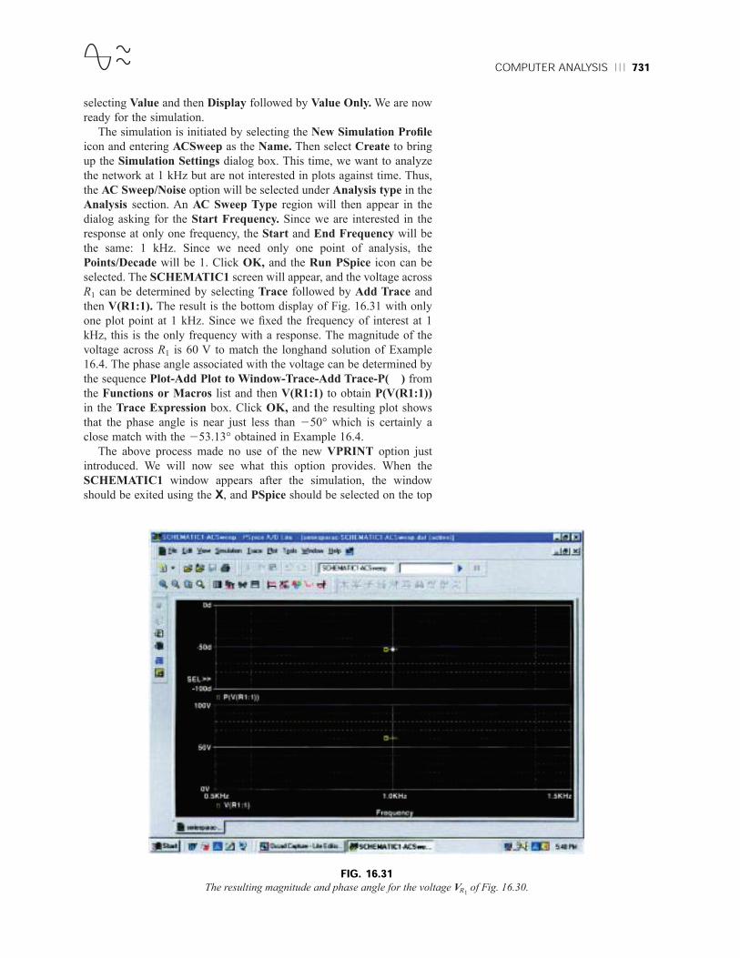
COMPUTER ANALYSIS 731
selecting Value and then Display followed by Value Only. We are now
ready for the simulation.
The simulation is initiated by selecting the New Simulation Profile
icon and entering ACSweep as the Name. Then select Create to bring
up the Simulation Settings dialog box. This time, we want to analyze
the network at 1 kHz but are not interested in plots against time. Thus,
the AC Sweep/Noise option will be selected under Analysis type in the
Analysis section. An AC Sweep Type region will then appear in the
dialog asking for the Start Frequency. Since we are interested in the
response at only one frequency, the Start and End Frequency will be
the same: 1 kHz. Since we need only one point of analysis, the
Points/Decade will be 1. Click OK, and the Run PSpice icon can be
selected. The SCHEMATIC1 screen will appear, and the voltage across
R1 can be determined by selecting Trace followed by Add Trace and
then V(R1:1). The result is the bottom display of Fig. 16.31 with only
one plot point at 1 kHz. Since we fixed the frequency of interest at 1
kHz, this is the only frequency with a response. The magnitude of the
voltage across R1 is 60 V to match the longhand solution of Example
16.4. The phase angle associated with the voltage can be determined by
the sequence Plot-Add Plot to Window-Trace-Add Trace-P( ) from
the Functions or Macros list and then V(R1:1) to obtain P(V(R1:1))
in the Trace Expression box. Click OK, and the resulting plot shows
that the phase angle is near just less than 250° which is certainly a
close match with the 253.13° obtained in Example 16.4.
The above process made no use of the new VPRINT option just
introduced. We will now see what this option provides. When the
SCHEMATIC1 window appears after the simulation, the window
should be exited using the X, and PSpice should be selected on the top
FIG. 16.31The resulting magnitude and phase angle for the voltage VR1
of Fig. 16.30.

732 SERIES-PARALLEL ac NETWORKS
menu bar of the resulting screen. A list will appear of which View Out-
put File is an option. Selecting this option will result in a long list of
data about the construction of the network and the results obtained from
the simulation. In Fig. 16.32 the portion of the output file listing the
resulting magnitude and phase angle for the voltages defined by
VPRINT1 and VPRINT2 is provided. Note that the voltage across R1
defined by VPRINT1 is 60 V at an angle of 53.13°. The voltage across
R2 as defined by VPRINT2 is 80 V at an angle of 36.87°. Both are
exact matches of the solutions of Example 16.4. In the future, therefore,
if the VPRINT option is used, the results will appear in the output file.
Now we will determine the voltage across the two branches from
point a to point b. Return to SCHEMATIC1, and select Trace fol-
lowed by Add Trace to obtain the list of Simulation Output Vari-
ables. Then, by applying Kirchhoff’s voltage law around the closed
loop, we find that the desired voltage is V(R1:1)-V(R2:1) which when
followed by OK will result in the plot point in the screen in the bot-
tom of Fig. 16.33. Note that it is exactly 100 V as obtained in the
longhand solution. The phase angle can then be determined through
Plot-Add Plot to Window-Trace-Add Trace and creating the expres-
sion P(V(R1:1)-V(R2:1)). Remember that the expression can be gen-
erated using the lists of Output variables and Functions, but it can
FIG. 16.32The VPRINT1 (VR1
) and VPRINT2 (VR2) response for the network of Fig. 16.30.

COMPUTER ANALYSIS 733
also be simply typed in from the keyboard. However, always be sure
that there are as many left parentheses as there are right. Click OK, and
a solution near 2105° appears. A better reading can be obtained by
using Plot-Axis Settings-Y Axis-User Defined and changing the scale
to 2100° to 2110°. The result is the top screen of Fig. 16.33 with an
angle closer to 2106.5° or 73.5° which is very close to the theoretical
solution of 73.74°.
Finally, the last way to find the desired bridge voltage is to remove
the VPRINT2 option and place the ground at that point as shown in
Fig. 16.34. Now the voltage generated from a point above R1 to ground
will be the desired voltage. Repeating a full simulation will then result
in the plot of Fig. 16.35 with the the same results as Fig. 16.33. Note,
however, that even though the two figures look the same, the quantities
listed in the bottom left of each plot are different.
Electronics WorkbenchElectronics Workbench will now be used to determine the voltage
across the last element of the ladder network of Fig. 16.36. The mathe-
matical content of this chapter would certainly suggest that this analy-
sis would be a lengthy exercise in complex algebra, with one mistake (a
single sign or an incorrect angle) enough to invalidate the results. How-
ever, it will take only a few minutes to “draw” the network on the
screen and only a few seconds to generate the results—results you can
usually assume are correct if all the parameters were entered correctly.
The results are certainly an excellent check against a longhand solution.
FIG. 16.33The PSpice reponse for the voltage between the two points above resistors
R1 and R2.

734 SERIES-PARALLEL ac NETWORKS
FIG. 16.34Determining the voltage between the two points above resistors R1 and R2 by
moving the ground connection of Fig. 16.30 to the position of VPRINT2.
FIG. 16.35PSpice response to the simulation of the network of Fig. 16.34.

COMPUTER ANALYSIS 735
Our first approach will be to use an oscilloscope to measure the
amplitude and phase angle of the output voltage as shown in Fig. 16.36.
Note that five nodes are defined, with node 5 the desired voltage. The
oscilloscope settings include a Time base of 20 ms/div. since the period
of the 10-kHz signal is 100 ms. Channel A was set on 10 V/div. so that
the full 20 V of the applied signal will have a peak value encompassing
two divisions. Note that Channel A in Fig. 16.36 is connected directly
to the source Vs and to the Trigger input for synchronization. Expect-
ing the output voltage to have a smaller amplitude resulted in a vertical
sensitivity of 1 V/div. for Channel B. The analysis was initiated by
placing the Simulation switch in the 1 position. It is important to real-
ize that
when simulation is initiated, it will take time for networks with
reactive elements to settle down and for the response to reach its
steady-state condition. It is therefore wise to let a system run for a
while after simulation before selecting Single on the oscilloscope to
obtain a steady waveform for analysis.
The resulting plots of Fig. 16.37 clearly show that the applied voltage
has an amplitude of 20 V and a period of 100 ms (5 div. at 20 ms/div).
The cursors sit ready for use at the left and right edges of the screen.
Clicking on the small red arrow (with number 1) at the top of the oscil-
loscope screen will permit you to drag it to any location on the hori-
zontal axis. As you move the cursor, the magnitude of each waveform
will appear in the T1 box below. By comparing positive slopes through
the origin, you should see that the applied voltage is leading the output
voltage by an angle that is more than 90°. Setting the cursor at the
FIG. 16.36Using the oscilloscope of Electronics Workbench to determine the voltage
across the capacitor C2.

736 SERIES-PARALLEL ac NETWORKS
point where the output voltage on channel B passes through the origin
with a positive slope, we find that we cannot achieve exactly 0 V; but
2313.4 mV 5 20.313 mV (VB1) is certainly very close at 39.7 ms
(T1).
Knowing that the applied voltage passed through the origin at 0 ms
permits the following claculation for the phase angle:
5v
360°
39.7 ms100 ms
FIG. 16.37Using Electronics Workbench to display the applied voltage and voltage across
the capacitor C2 for the network of Fig. 16.36.
v 5 142.92°
with the result that the output voltage has an angle of 2142.92° associ-
ated with it. The second cursor is found at the right edge of the screen
and has a blue color. Selecting it and moving it to the peak value of the
output voltage results in VB2 5 1.2 V at 65.7 ms (T2). The result of all
the above is
VC25 1.2 V /2142.92°.
Our second approach will be to use the AC Analysis option under
the Simulate heading. First, realize that when we were using the oscil-
loscope as we did above, there was no need to pass through the
sequence of dialog boxes to choose the desired analysis. All that was
necessary was to simulate using either the switch or the PSpice-Run
sequence—the oscilloscope was there to measure the output voltage.
Remember that the source defined the magnitude of the applied voltage,
the frequency, and the phase shift. This time we will use the sequence

COMPUTER ANALYSIS 737
Simulate-Analyses-AC Analysis to obtain the AC Analysis dialog box
in which the Start and Stop frequencies will be 10 kHz and the
Selected variable for analysis will be node 5 only. Selecting Simulate
will then result in a magnitude-phase plot with no apparent indicators at
10 kHz. However, this is easily corrected by first selecting one of the
plots by clicking on the Voltage label at the left of the plot. Then select
the Show/Hide Grid, Show/Hide Legend, and Show/Hide Cursors
keys to obtain the cursors, legend, and AC Analysis dialog box. Hook on
the red cursor and move it to 10 kHz. At that location, and that location
only, x1 will appear as 10 kHz in the dialog box, and y1 will be 1.1946
as shown in Fig. 16.38. In other words, the cursor has defined the mag-
nitude of the voltage across the output capacitor as 1.1946 V or approx-
imately 1.2 V as obtained above. If you then select the Phase curve and
repeat the procedure, you will find that at 10 kHz (x1) the angle is
2142.15° (y1) which is very close to the 2142.92° obtained above.
FIG. 16.38Using the AC Analysis option under Electronics Workbench to determine
the magnitude and phase angle for the voltage VC2for the network of
Fig. 16.36.
In total, therefore, we have two methods to obtain an ac voltage in a
network—one by instrumentation and the other through the computer
methods. Both are valid, although, as expected, the computer approach
has a higher level of accuracy.

738 SERIES-PARALLEL ac NETWORKS
PROBLEMSSECTION 16.2 Illustrative Examples
1. For the series-parallel network of Fig. 16.39:
a. Calculate ZT.
b. Determine I.
c. Determine I1.
d. Find I2 and I3.
e. Find VL.
I
+ –
E = 12 V ∠ 0°
8 V
ZT
VL XC1
12 VXC2
I1 I2
I3
+
–
XL = 6 V
FIG. 16.39Problems 1 and 19.
2. For the network of Fig. 16.40:
a. Find the total impedance ZT.
b. Determine the current Is.
c. Calculate IC using the current divider rule.
d. Calculate VL using the voltage divider rule.
R2
2 V+ –
E = 30 V ∠ 0° 8 V
ZT
VL
XCIs
IC
+
–
XL = 6 V
R1
3 V
FIG. 16.40Problems 2 and 15.
3. For the network of Fig. 16.41:
a. Find the total impedance ZT and the total admittance
YT.
b. Find the current Is.
c. Calculate I2 using the current divider rule.
d. Calculate VC.
e. Calculate the average power delivered to the network.
Is
+
–
E = 60 V ∠ 30° R1 4.7 V
R2 9.1 V
XC = 12 VVC
+
–
ZT
YT
I2
FIG. 16.41Problems 3 and 20.

PROBLEMS 739
4. For the network of Fig. 16.42:
a. Find the total impedance ZT.
b. Calculate the voltage V2 and the current IL.
c. Find the power factor of the network.
5. For the network of Fig. 16.43:
a. Find the current I.
b. Find the voltage VC.
c. Find the average power delivered to the network.
+ V2 –
R2 = 8 V
I = 5 A ∠ 0°
4 V
ZT
XC
IL
+
–
6 V
R1
2 V R3 = 8 V
XL2 = 3 V
XL1
FIG. 16.42Problem 4.
R1 560 V+
–
E = 100 V ∠ 0°+
–
XL
I
560 V VC
R2 200 V
XC2 = 400 VXC1
= 400 V
FIG. 16.43Problems 5 and 21.
*6. For the network of Fig. 16.44:
a. Find the current I1.
b. Calculate the voltage VC using the voltage divider rule.
c. Find the voltage Vab.
*7. For the network of Fig. 16.45:
a. Find the current I1.
b. Find the voltage V1.
c. Calculate the average power delivered to the network.
FIG. 16.44Problem 6.
R1 3 V
XL14 V
I1
Vaba b
XC 13 V+
–
E = 120 V ∠ 60°
XL27 V
VC
+
–
FIG. 16.45Problems 7 and 16.
V1
XC
60 V
XL = 80 V
I1
R2
20 V+
–
E = 40 V ∠ 0°+
–
R1
10 V

740 SERIES-PARALLEL ac NETWORKS
8. For the network of Fig. 16.46:
a. Find the total impedance ZT and the admittance YT.
b. Find the currents I1, I2, and I3.
c. Verify Kirchhoff’s current law by showing that Is 5
I1 1 I2 1 I3.
d. Find the power factor of the network, and indicate
whether it is leading or lagging.
*9. For the network of Fig. 16.47:
a. Find the total admittance YT.
b. Find the voltages V1 and V2.
c. Find the current I3.
I1Is
ZT
+
–
E = 60 V ∠ 0°
1 V
XC 7 V
I2
R2 3 V
XL1
YT
R3 16 V
R1 2 V
15 V
XL2
I3
FIG. 16.46Problem 8.
*10. For the network of Fig. 16.48:
a. Find the total impedance ZT and the admittance YT.
b. Find the source current Is in phasor form.
c. Find the currents I1 and I2 in phasor form.
d. Find the voltages V1 and Vab in phasor form.
e. Find the average power delivered to the network.
f. Find the power factor of the network, and indicate
whether it is leading or lagging.
+
–I = 3 A ∠ 30°
I3– V1 +
R1 = 6.8 V
R3
3 V
4 V
XC1
R4
3 V
4 V
XC2
7 V XL V2 R2 = 8.2 V
YT
FIG. 16.47Problem 9.
is
ZT+
–
e = =2(50) sin 2p 1000t
L1 = 0.1 H
i1
YT
R1
300 Va
b
vab
i2
C 1 mF v1
+
–L2 = 0.2 H
FIG. 16.48Problem 10.
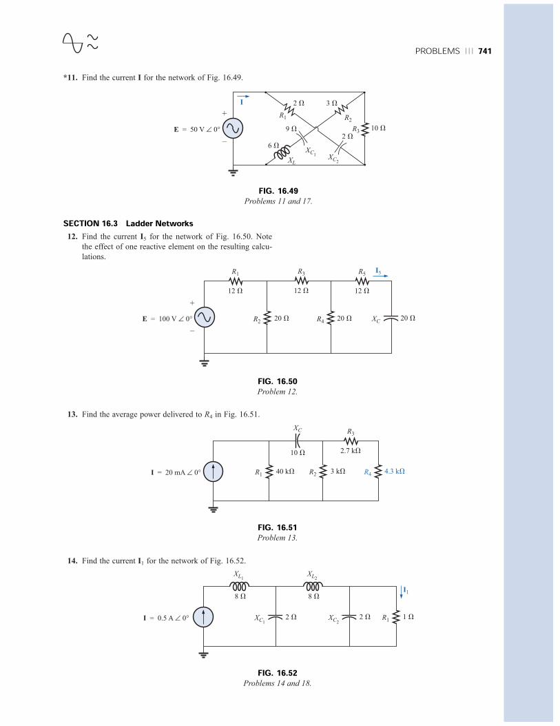
PROBLEMS 741
*11. Find the current I for the network of Fig. 16.49.
XC1
9 V
XL
I
R310 V
+
–
E = 50 V ∠ 0°
R1
2 V
6 V
XC2
2 V
R2
3 V
FIG. 16.49Problems 11 and 17.
SECTION 16.3 Ladder Networks12. Find the current I5 for the network of Fig. 16.50. Note
the effect of one reactive element on the resulting calcu-
lations.
13. Find the average power delivered to R4 in Fig. 16.51.
I5
E = 100 V ∠ 0° XC 20 VR4 20 VR2 20 V
R1
12 V
R3
12 V
R5
12 V
+
–
FIG. 16.50Problem 12.
I = 20 mA ∠ 0°
XC
10 V
R1 40 kV
R3
2.7 kV
R2 3 kV R4 4.3 kV
FIG. 16.51Problem 13.
I = 0.5 A ∠ 0° XC12 V
8 V
R1 1 VXC22 V
XL2
8 V
XL1
I1
FIG. 16.52Problems 14 and 18.
14. Find the current I1 for the network of Fig. 16.52.

742 SERIES-PARALLEL ac NETWORKS
SECTION 16.5 Computer AnalysisPSpice or Electronics WorkbenchFor Problems 15 through 18, use a frequency of 1 kHz to
determine the inductive and capacitive levels required for the
input files. In each case write the required input file.
*15. Repeat Problem 2 using PSpice or EWB.
*16. Repeat Problem 7, parts (a) and (b), using PSpice or
EWB.
*17. Repeat Problem 11 using PSpice or EWB.
*18. Repeat Problem 14 using PSpice or EWB.
Programming Language (C11, QBASIC, Pascal, etc.)19. Write a program to provide a general solution to Problem
1; that is, given the reactance of each element, generate a
solution for parts (a) through (e).
20. Given the network of Fig. 16.41, write a program to gen-
erate a solution for parts (a) and (b) of Problem 2. Use
the values given.
21. Generate a program to obtain a general solution for the
network of Fig. 16.43 for the questions asked in parts (a)
through (c) of Problem 2. That is, given the resistance
and reactance of the elements, determine the requested
current, voltage, and power.
GLOSSARYLadder network A repetitive combination of series and par-
allel branches that has the appearance of a ladder.
Series-parallel ac network A combination of series and par-
allel branches in the same network configuration. Each
branch may contain any number of elements whose imped-
ance is dependent on the applied frequency.

17
17.1 INTRODUCTIONFor networks with two or more sources that are not in series or parallel,
the methods described in the last two chapters cannot be applied.
Rather, methods such as mesh analysis or nodal analysis must be
employed. Since these methods were discussed in detail for dc circuits
in Chapter 8, this chapter will consider the variations required to apply
these methods to ac circuits. Dependent sources will also be introduced
for both mesh and nodal analysis.
The branch-current method will not be discussed again because it
falls within the framework of mesh analysis. In addition to the methods
mentioned above, the bridge network and D-Y, Y-D conversions will
also be discussed for ac circuits.
Before we examine these topics, however, we must consider the sub-
ject of independent and controlled sources.
17.2 INDEPENDENT VERSUS DEPENDENT(CONTROLLED) SOURCESIn the previous chapters, each source appearing in the analysis of dc or
ac networks was an independent source, such as E and I (or E and I)
in Fig. 17.1.
NA
FIG. 17.1Independent sources.
E
+
–
E
+
–
I I
Methods of Analysis andSelected Topics (ac)

744 METHODS OF ANALYSIS AND SELECTED TOPICS (ac)
The term independent specifies that the magnitude of the source is
independent of the network to which it is applied and that the source
displays its terminal characteristics even if completely isolated.
A dependent or controlled source is one whose magnitude is
determined (or controlled) by a current or voltage of the system in
which it appears.
Currently two symbols are used for controlled sources. One simply
uses the independent symbol with an indication of the controlling ele-
ment, as shown in Fig. 17.2. In Fig. 17.2(a), the magnitude and phase
of the voltage are controlled by a voltage V elsewhere in the system,
with the magnitude further controlled by the constant k1. In Fig.
NA
k1V
+
–
I
(a)
V+ –
k2I
(b)
FIG. 17.2Controlled or dependent sources.
Possible combinations for controlled sources are indicated in Fig.
17.4. Note that the magnitude of current sources or voltage sources can
be controlled by a voltage and a current, respectively. Unlike with the
independent source, isolation such that V or I 5 0 in Fig. 17.4(a) will
result in the short-circuit or open-circuit equivalent as indicated in Fig.
17.4(b). Note that the type of representation under these conditions is
controlled by whether it is a current source or a voltage source, not by
the controlling agent (V or I).
k1V
+
–
I
(a)
V+ –
k2I
(b)
FIG. 17.3Special notation for controlled or dependent sources.
17.2(b), the magnitude and phase of the current source are controlled by
a current I elsewhere in the system, with the magnitude further con-
trolled by the constant k2. To distinguish between the dependent and
independent sources, the notation of Fig. 17.3 was introduced. In recent
years many respected publications on circuit analysis have accepted the
notation of Fig. 17.3, although a number of excellent publications in the
area of electronics continue to use the symbol of Fig. 17.2, especially in
the circuit modeling for a variety of electronic devices such as the tran-
sistor and FET. This text will employ the symbols of Fig. 17.3.

SOURCE CONVERSIONS 745
17.3 SOURCE CONVERSIONSWhen applying the methods to be discussed, it may be necessary to
convert a current source to a voltage source, or a voltage source to a
current source. This source conversion can be accomplished in much
the same manner as for dc circuits, except now we shall be dealing with
phasors and impedances instead of just real numbers and resistors.
Independent SourcesIn general, the format for converting one type of independent source to
another is as shown in Fig. 17.5.
EXAMPLE 17.1 Convert the voltage source of Fig. 17.6(a) to a current
source.
NA
V
+
–
k1V +–
k2V
I
k3I +–
k4I
(a) (b)
FIG. 17.4Conditions of V 5 0 V and I 5 0 A for a controlled source.
+
–
Voltage source
a
E = IZ
a9
I =E
Z
Z
Z
a
a9
Current source
FIG. 17.5Source conversion.
I = 20 A ∠ –53.13°
E = 100 V ∠ 0°+
–
(a)
a
R 3 V
a9
XL 4 V
a
a9
XL 4 V
R 3 V
Z
Z
Source conversion
(b)
FIG. 17.6Example 17.1.

746 METHODS OF ANALYSIS AND SELECTED TOPICS (ac)
Solution:I 5 5
5 20 A /253.13° [Fig. 17.6(b)]
EXAMPLE 17.2 Convert the current source of Fig. 17.7(a) to a voltage
source.
100 V /0°5 V /53.13°
EZ
NA
XL 4 VI = 10 A ∠ 60°
a9
a
(a)
6 V
Z
E = 120 V ∠ –30°
a9
a
(b)
XC = 12 V
Z
+
–
XC
FIG. 17.7Example 17.2.
Solution:Z 5
Z
Z
C
C
1
Z
Z
L
L
5 (XC /290°)(XL /90°)
2j XC 1 j XL
5 5
5 12 V /290° [Fig. 17.7(b)]
E 5 IZ 5 (10 A /60°)(12 V /290°)
5 120 V/230° [Fig. 17.7(b)]
Dependent SourcesFor dependent sources, the direct conversion of Fig. 17.5 can be applied
if the controlling variable (V or I in Fig. 17.4) is not determined by a
portion of the network to which the conversion is to be applied. For
example, in Figs. 17.8 and 17.9, V and I, respectively, are controlled by
an external portion of the network. Conversions of the other kind,
where V and I are controlled by a portion of the network to be con-
verted, will be considered in Sections 18.3 and 18.4.
24 V / 0°
2 / 90°
(4 V /290°)(6 V /90°)
2j 4 V 1 j 6 V

MESH ANALYSIS 747NA
20 V
+
–V = V ∠ 0°
+
–
(a)
Z = 5 kV
(4 3 10–3 V) A ∠ 0°
+
–V = V ∠ 0°
+
–Z 5 kV
(b)
FIG. 17.8Source conversion with a voltage-controlled voltage source.
(4 3 106I) V ∠ 0°
+
–
(b)
40 kV
(100I) Α ∠ 0° Z 40 kV
I = I ∠ 0° I I ∠ 0°
(a)
Z
FIG. 17.9Source conversion with a current-controlled current source.
Solution:I 5
E
Z 5
5 (4 3 1023
V) A /0° [Fig. 17.8(b)]
EXAMPLE 17.4 Convert the current source of Fig. 17.9(a) to a voltage
source.
(20V) V /0°
5 kV /0°
Solution:E 5 IZ 5 [(100I) A /0°][40 kV /0°]
5 (4 3 106I) V /0° [Fig. 17.9(b)]
17.4 MESH ANALYSISGeneral ApproachIndependent Voltage Sources Before examining the application
of the method to ac networks, the student should first review the appro-
priate sections on mesh analysis in Chapter 8 since the content of this
section will be limited to the general conclusions of Chapter 8.
The general approach to mesh analysis for independent sources
includes the same sequence of steps appearing in Chapter 8. In fact,
throughout this section the only change from the dc coverage will be to
substitute impedance for resistance and admittance for conductance in
the general procedure.
EXAMPLE 17.3 Convert the voltage source of Fig. 17.8(a) to a current
source.

748 METHODS OF ANALYSIS AND SELECTED TOPICS (ac)
1. Assign a distinct current in the clockwise direction to each
independent closed loop of the network. It is not absolutely
necessary to choose the clockwise direction for each loop current.
However, it eliminates the need to have to choose a direction for
each application. Any direction can be chosen for each loop
current with no loss in accuracy as long as the remaining steps are
followed properly.
2. Indicate the polarities within each loop for each impedance as
determined by the assumed direction of loop current for that loop.
3. Apply Kirchhoff’s voltage law around each closed loop in the
clockwise direction. Again, the clockwise direction was chosen to
establish uniformity and to prepare us for the format approach to
follow.
a. If an impedance has two or more assumed currents through it,
the total current through the impedance is the assumed current
of the loop in which Kirchhoff’s voltage law is being applied,
plus the assumed currents of the other loops passing through in
the same direction, minus the assumed currents passing
through in the opposite direction.
b. The polarity of a voltage source is unaffected by the direction of
the assigned loop currents.
4. Solve the resulting simultaneous linear equations for the assumed
loop currents.
The technique is applied as above for all networks with independent
sources or for networks with dependent sources where the controlling
variable is not a part of the network under investigation. If the control-
ling variable is part of the network being examined, a method to be
described shortly must be applied.
EXAMPLE 17.5 Using the general approach to mesh analysis, find the
current I1 in Fig. 17.10.
NA
I1 R = 4 V
XL = 2 V
E1 = 2 V ∠ 0°+
–
XC = 1 V
+
–E2 = 6 V ∠ 0°
FIG. 17.10Example 17.5.
Solution: When applying these methods to ac circuits, it is good
practice to represent the resistors and reactances (or combinations
thereof) by subscripted impedances. When the total solution is found in
terms of these subscripted impedances, the numerical values can be
substituted to find the unknown quantities.
The network is redrawn in Fig. 17.11 with subscripted impedances:
Z1 5 1j XL 5 1j 2 V E1 5 2 V /0°
Z2 5 R 5 4 V E2 5 6 V /0°
Z3 5 2j XC 5 2j 1 V
Steps 1 and 2 are as indicated in Fig. 17.11.
Z1
E1
+
–
+
–E2
+
–
I1
Z2
+
–
–
+
I2
Z3
–
+
FIG. 17.11Assigning the mesh currents and subscripted
impedances for the network of Fig. 17.10.

MESH ANALYSIS 749
Step 3:
1E1 2 I1Z1 2 Z2(I1 2 I2) 5 0
2Z2(I2 2 I1) 2 I2Z3 2 E2 5 0
or E12 I1Z1 2 I1Z2 1 I2Z2 5 0
2I2Z2 1 I1Z2 2 I2Z3 2 E2 5 0
so that I1(Z1 1 Z2) 2 I2Z2 5 E1
I2(Z2 1 Z3) 2 I1Z2 5 2E2
which are rewritten as
I1(Z1 1 Z2) 2 I2Z2 5 E1
2I1Z2 1 I2(Z2 1 Z3) 5 2E2
Step 4: Using determinants, we obtain
E1 2Z2 2E2 Z2 1 Z3
I1 5 ––––––––––––––––––Z1 1 Z2 2Z2 2Z2 Z2 1 Z3
5
5
Substituting numerical values yields
I1 5
5 5 5
5 3.61 A /2236.30° or 3.61 A /123.70°
Dependent Voltage Sources For dependent voltage sources, the
procedure is modified as follows:
1. Steps 1 and 2 are the same as those applied for independent volt-
age sources.
2. Step 3 is modified as follows: Treat each dependent source like an
independent source when Kirchhoff’s voltage law is applied to
each independent loop. However, once the equation is written,
substitute the equation for the controlling quantity to ensure that
the unknowns are limited solely to the chosen mesh currents.
3. Step 4 is as before.
EXAMPLE 17.6 Write the mesh currents for the network of Fig. 17.12
having a dependent voltage source.
Solution:Steps 1 and 2 are defined on Fig. 17.12.
Step 3: E1 2 I1R1 2 R2(I1 2 I2) 5 0
R2(I2 2 I1) 1 mVx 2 I2R3 5 0
Then substitute Vx 5 (I1 2 I2)R2
16.12 A /2172.87°
4.47 /63.43°
216 2j 2
2 1 j 4
2162j 2j 8 2 j 22 2 j 4
(2 V 2 6 V)(4 V) 1 (2 V)(2j 1 V)(1j 2 V)(4 V) 1 (1j 2 V)(2j 2 V) 1 (4 V)(2j 2 V)
(E1 2 E2)Z2 1 E1Z3Z1Z2 1 Z1Z3 1 Z2Z3
E1(Z2 1 Z3) 2 E2(Z2)(Z1 1 Z2)(Z2 1 Z3) 2 (Z2)
2
NA
R1
R3R2
mVx
+
–
+–
E1 Vx
+
–
I1 I2
m
FIG. 17.12Applying mesh analysis to a network with a
voltage-controlled voltage source.

750 METHODS OF ANALYSIS AND SELECTED TOPICS (ac)
The result is two equations and two unknowns.
E1 2 I1R1 2 R2(I 2 I2) 5 0
R2(I2 2 I1) 1 mR2(I1 2 I2) 2 I2R3 5 0
Independent Current Sources For independent current sources,
the procedure is modified as follows:
1. Steps 1 and 2 are the same as those applied for independent
sources.
2. Step 3 is modified as follows: Treat each current source as an
open circuit (recall the supermesh designation of Chapter 8), and
write the mesh equations for each remaining independent path.
Then relate the chosen mesh currents to the dependent sources to
ensure that the unknowns of the final equations are limited sim-
ply to the mesh currents.
3. Step 4 is as before.
EXAMPLE 17.7 Write the mesh currents for the network of Fig. 17.13
having an independent current source.
Solution:Steps 1 and 2 are defined on Fig. 17.13.
Step 3: E1 2 I1Z1 1 E2 2 I2Z2 5 0 (only remaining independent
path)
with I1 1 I 5 I2
The result is two equations and two unknowns.
Dependent Current Sources For dependent current sources, the
procedure is modified as follows:
1. Steps 1 and 2 are the same as those applied for independent
sources.
2. Step 3 is modified as follows: The procedure is essentially the
same as that applied for independent current sources, except now
the dependent sources have to be defined in terms of the chosen
mesh currents to ensure that the final equations have only mesh
currents as the unknown quantities.
3. Step 4 is as before.
EXAMPLE 17.8 Write the mesh currents for the network of Fig. 17.14
having a dependent current source.
Solution:Steps 1 and 2 are defined on Fig. 17.14.
Step 3: E1 2 I1Z1 2 I2Z2 1 E2 5 0
and kI 5 I1 2 I2
Now I 5 I1 so that kI1 5 I1 2 I2 or I2 5 I1(1 2 k)
The result is two equations and two unknowns.
NA
E2 +–
E1
+
–
I1 I2Z2
Z1
I
FIG. 17.13Applying mesh analysis to a network with an
independent current source.
E2
+
E1
+
–
I1 I2
Z1
kI
–
Z2
I
FIG. 17.14Applying mesh analysis to a network with a
current-controlled current source.

MESH ANALYSIS 751
Format ApproachThe format approach was introduced in Section 8.9. The steps for
applying this method are repeated here with changes for its use in ac
circuits:
1. Assign a loop current to each independent closed loop (as in the
previous section) in a clockwise direction.
2. The number of required equations is equal to the number of
chosen independent closed loops. Column 1 of each equation is
formed by simply summing the impedance values of those
impedances through which the loop current of interest passes and
multiplying the result by that loop current.
3. We must now consider the mutual terms that are always subtracted
from the terms in the first column. It is possible to have more than
one mutual term if the loop current of interest has an element in
common with more than one other loop current. Each mutual
term is the product of the mutual impedance and the other loop
current passing through the same element.
4. The column to the right of the equality sign is the algebraic sum of
the voltage sources through which the loop current of interest
passes. Positive signs are assigned to those sources of voltage
having a polarity such that the loop current passes from the
negative to the positive terminal. Negative signs are assigned to
those potentials for which the reverse is true.
5. Solve the resulting simultaneous equations for the desired loop
currents.
The technique is applied as above for all networks with independent
sources or for networks with dependent sources where the controlling vari-
able is not a part of the network under investigation. If the controlling
variable is part of the network being examined, additional care must be
taken when applying the above steps.
EXAMPLE 17.9 Using the format approach to mesh analysis, find the
current I2 in Fig. 17.15.
NA
Solution 1: The network is redrawn in Fig. 17.16:
Z1 5 R1 1 j XL15 1 V 1 j 2 V E1 5 8 V /20°
Z2 5 R2 2 j XC 5 4 V 2 j 8 V E2 5 10 V /0°
Z3 5 1j XL 25 1j 6 V
I2
4 V
E1 = 8 V ∠ 20°+
–
8 V
–
+E2 = 10 V ∠ 0°
R2
XC
XL1 = 2 V
1 VR1
XL26 V
FIG. 17.15Example 17.9.
Z1
E1
+
–
–
+E2
+
–
I1
Z2
+
–
–
+
I2
Z3
–
+
FIG. 17.16Assigning the mesh currents and subscripted
impedances for the network of Fig. 17.15.

752 METHODS OF ANALYSIS AND SELECTED TOPICS (ac)
Note the reduction in complexity of the problem with the substitution of
the subscripted impedances.
Step 1 is as indicated in Fig. 17.16.
Steps 2 to 4:
I1(Z1 1 Z2) 2 I2Z2 5 E1 1 E2
I2(Z2 1 Z3) 2 I1Z2 5 2E2
which are rewritten as
I1(Z1 1 Z2) 2 I2Z2 5 E1 1 E2
2I1Z2 1 I2(Z2 1 Z3) 5 2E2
Step 5: Using determinants, we have
Z1 1 Z2 E1 1 E2 2Z2 2E2
I2 5 ––––––––––––––––––Z1 1 Z2 2Z2 2Z2 Z2 1 Z3
5
5
Substituting numerical values yields
Z2E1 2 Z1E2Z1Z2 1 Z1Z3 1 Z2Z3
2(Z1 1 Z2)E2 1 Z2(E1 1 E2)
(Z1 1 Z2)(Z2 1 Z3) 2 Z22
NA
((4,28)*8(/20)2(1,2)*(10/0))/((1,2)*(4,28)1(1,2)*(0,6)1(4,28)*(0,6)) ENTER(67.854E23,21.272E0)Ans c Pol(1.274E0/286.956E0)
CALC. 17.1
I2 5
5
5 5 5
5 1.27 A /286.92°
80.95 A /258.74°
63.53 /28.18°
42.0 2 j 69.20
56 1 j 30
(52.0 2 j 49.20) 2 (10 1 j 20)
56 1 j 30
(4 2 j 8)(7.52 1 j 2.74) 2 (10 1 j 20)
20 1 ( j 6 2 12) 1 ( j 24 1 48)
(4 V 2 j 8 V)(8 V / 20°) 2 (1 V 1 j 2 V)(10 V /0°)(1 V 1 j 2 V)(4 V 2 j 8 V) 1 (1 V 1 j 2 V)(1 j 6 V) 1 (4 V 2 j 8 V)(1j 6 V)
Mathcad Solution: This example provides an excellent opportunity
to demonstrate the power of Mathcad. First the impedances and para-
meters are defined for the equations to follow as shown in Fig. 17.17.
Then the guess values of the mesh currents I1 and I2 are entered. The
label Given must then be entered followed by the equations for the net-
Calculator The calculator (TI-86 or equivalent) can be an effective tool
in performing the long, laborious calculations involved with the final
equation appearing above. However, you must be very careful to use the
correct number of brackets and to define by brackets the order of the arith-
metic operations.

MESH ANALYSIS 753
work. Note that in this example, we are not continuing with the analy-
sis until the matrix is defined—we are working directly from the net-
work equations. Once the equations have been properly entered,
Find(I1,I2) is entered. Then selecting the equal sign will result in the
single-column matrix with the results in rectangular form. Conversion
to polar form requires defining a variable A and then calling for the
magnitude and angle using the definitions entered earlier in the list-
ing and both the Calculator and Greek toolbars. The result for I2 is
1.274 A /286.94° which is an excellent match with the theoretical
solution.
EXAMPLE 17.10 Write the mesh equations for the network of Fig.
17.18. Do not solve.
NA
FIG. 17.17Using Mathcad to verify the results of Example 17.9.
E1
+
–
–
+E2
R2
R1
XL2
XL1
XC1
R3
XC2
R4
FIG. 17.18Example 17.10.

754 METHODS OF ANALYSIS AND SELECTED TOPICS (ac)
Solution: The network is redrawn in Fig. 17.19. Again note the
reduced complexity and increased clarity provided by the use of sub-
scripted impedances:
Z1 5 R1 1 j XL1Z4 5 R3 2 j XC2
Z2 5 R2 1 j XL2Z5 5 R4
Z3 5 j XC1
and I1(Z1 1 Z2) 2 I2Z2 5 E1
I2(Z2 1 Z3 1 Z4) 2 I1Z2 2 I3Z4 5 0
I3(Z4 1 Z5) 2 I2Z4 5 E2
or I1(Z1 1 Z2) 2 I2(Z2) 1 0 5 E1
I1Z2 2 I2(Z2 1 Z3 1 Z4) 1 I3(Z4) 5 0
0 2 I2(Z4) 1 I3(Z4 1 Z5) 5 E2
NA
Z2
+
–
–
+
Z1
E1
+
–
–
+E2
+ –
I1 I2
Z4
+
–
–
+
Z3+ –
Z5+ –
I3
FIG. 17.19Assigning the mesh currents and subscripted impedances for the network of
Fig. 17.18.
EXAMPLE 17.11 Using the format approach, write the mesh equa-
tions for the network of Fig. 17.20.
Solution: The network is redrawn as shown in Fig. 17.21, where
Z1 5 R1 1 j XL 1Z3 5 j XL2
Z2 5 R2 Z4 5 j XL3
and I1(Z2 1 Z4) 2 I2Z2 2 I3Z4 5 E1
I2(Z1 1 Z2 1 Z3) 2 I1Z2 2 I3Z3 5 0
I3(Z3 1 Z4) 2 I2Z3 2 I1Z4 5 E2
or
Note the symmetry about the diagonal axis; that is, note the location of
2Z2, 2Z4, and 2Z3 off the diagonal.
17.5 NODAL ANALYSISGeneral ApproachIndependent Sources Before examining the application of the
method to ac networks, a review of the appropriate sections on nodal
I1(Z2 1 Z4) 2 I2Z2 2 I3Z4 5 E1
2I1Z2 1 I2(Z1 1 Z2 1 Z3) 2 I3Z3 5 0
2I1Z4 2 I2Z3 1 I3(Z3 1 Z4) 5 E2
E1
+
–
–
+E2
R1
XL3
XL1
R2XL2
FIG. 17.20Example 17.11
Z2
E1
+
–
–
+E2
I1
Z4
I2
I3
Z3
Z1
FIG. 17.21Assigning the mesh currents and subscripted
impedances for the network of Fig. 17.20.

NODAL ANALYSIS 755
analysis in Chapter 8 is suggested since the content of this section will
be limited to the general conclusions of Chapter 8.
The fundamental steps are the following:
1. Determine the number of nodes within the network.
2. Pick a reference node and label each remaining node with a
subscripted value of voltage: V1, V2, and so on.
3. Apply Kirchhoff’s current law at each node except the reference.
Assume that all unknown currents leave the node for each
application of Kirchhoff’s current law.
4. Solve the resulting equations for the nodal voltages.
A few examples will refresh your memory about the content of
Chapter 8 and the general approach to a nodal-analysis solution.
EXAMPLE 17.12 Determine the voltage across the inductor for the
network of Fig. 17.22.
NA
E =12 V ∠0°
+
–
R1
XL XC
0.5 kV
10 kV
R2
2 kV
5 kV I =4 mA ∠0°
FIG. 17.22Example 17.12.
Z2E
+
–
Z1Z1 Z3
Z4 I
V2V1
FIG. 17.23Assigning the nodal voltages and subscripted impedances to the network of
Fig. 17.22.
Solution 1:Steps 1 and 2 are as indicated in Fig. 17.23.
Z2E
+
–
Z1Z1 Z3
V2V1
I1 I3
I2
FIG. 17.24Applying Kirchhoff’s current law to the node
V1 of Fig. 17.23.
Step 3: Note Fig. 17.24 for the application of Kirchhoff’s current law
to node V1:
S Ii 5 S Io
0 5 I1 1 I2 1 I3
1 1 5 0V1 2 V2
Z3
V1Z2
V1 2 E
Z1

756 METHODS OF ANALYSIS AND SELECTED TOPICS (ac) NA
Rearranging terms:
V13 1 1 4 2 V23 4 5 (17.1)
Note Fig. 17.25 for the application of Kirchhoff’s current law to
node V2.
0 5 I3 1 I4 1 I
1 1 I 5 0
Rearranging terms:
V23 1 4 2 V13 4 5 2I (17.2)
Grouping equations:
V13 1 1 42 V23 4 5
V13 4 2 V23 1 4 5 I
1 1 5 1 1 5 2.5 mS /22.29°
1 5 1 5 0.539 mS /21.80°
and
V1[2.5 mS /22.29°] 2 V2[0.5 mS /0°] 5 24 mA /0°
V1[0.5 mS /0°] 2 V2[0.539 mS /21.80°] 5 4 mA /0°
with
24 mA /0° 20.5 mS /0° 4 mA /0° 20.539 mS /21.80°
V1 5 —————————————————–2.5 mS /22.29° 20.5 mS /0° 0.5 mS /0° 20.539 mS /21.80°
12j 5 kV
12 kV
1Z4
1Z3
12 kV
1j 10 kV
10.5 kV
1Z3
1Z2
1Z1
1Z4
1Z3
1Z3
EZ1
1Z3
1Z3
1Z2
1Z1
1Z3
1Z4
1Z3
V2Z4
V2 2 V1
Z3
E1Z1
1Z3
1Z3
1Z2
1Z1
FIG. 17.25Applying Kirchhoff’s current law to the node
V2 of Fig. 17.23.
Z3
Z4 I
V2V1
I3
I4
5
5
5
5 5
V1 5 9.95 V /1.88°
11.106 V /2154.33°
1.116 /2156.21°
210.01 V 2 j 4.81 V
21.021 2 j 0.45
2(12.01 1 j 4.81) 3 1026 V 1 2 3 1026 V2(1.271 1 j 0.45) 3 1026
1 0.25 3 1026
212.94 3 1026 V /21.80° 1 2 3 1026 V /0°21.348 3 1026
/19.51° 1 0.25 3 1026/0°
(24 mA /0°)(20.539 mS /21.80°) 1 (0.5 mS /0°)(4 mA /0°)(2.5 mS /22.29°)(20.539 mS /21.80°) 1 (0.5 mS /0°)(0.5 mS /0°)
Mathcad Solution: The length and the complexity of the above
mathematical development strongly suggest the use of an alternative
approach such as Mathcad. The printout of Fig. 17.26 first defines the
letters k and m to specific numerical values so that the power-of-ten
format did not have to be included in the equations. Thus, the results are
cleaner and easier to review. When entering the equations, remember
that the j is entered as 1j without the multiplication sign between the

NODAL ANALYSIS 757NA
FIG. 17.26Using Mathcad to verify the results of Example 17.12.
1 and the j. A multiplication sign between the two will define the j as
another variable. Also be sure that the multiplication process is inserted
between the nodal variables and the brackets. If an error signal contin-
ues to surface, it is often best to simply reenter the entire listing—errors
are often not easy to spot simply by looking at the resulting equations.
Finally the results are obtained and converted to polar form for com-
parison with the theoretical solution. The solution of 9.949 A /1.837°
is a very close confirmation of the longhand solution.
Before leaving this example, let’s look at another method for obtain-
ing the polar form of the solution. The method appears in the bottom of
Fig. 17.26. First deg is defined as shown, and then arg is picked up
from the Insert-f(x)-Insert Function-arg sequence. Next V1 is
entered; the result will be in radian form but with a small black rectan-
gle in the place where the units normally appear. Click on that black
rectangle, and the bracket will appear and deg can be typed. When the
equal sign is selected, the angle in degrees will appear.
Dependent Current Sources For dependent current sources, the
procedure is modified as follows:
1. Steps 1 and 2 are the same as those applied for independent
sources.
2. Step 3 is modified as follows: Treat each dependent current source
like an independent source when Kirchhoff’s current law is applied
to each defined node. However, once the equations are established,
substitute the equation for the controlling quantity to ensure that
the unknowns are limited solely to the chosen nodal voltages.
3. Step 4 is as before.

Solution:Steps 1 and 2 are as defined in Fig. 17.27.
Step 3: At node V1,
I 5 I1 1 I2
1 2 I 5 0
and V13 1 4 2 V23 4 5 I
At node V2,
I2 1 I3 1 kI95 0
1 1 k 3 4 5 0
and V13 4 2 V23 1 45 0
resulting in two equations and two unknowns.
1Z3
1 2 k
Z2
1 2 k
Z2
V1 2 V2
Z2
V2Z3
V2 2 V1
Z2
1Z2
1Z2
1Z1
V1 2 V2
Z2
V1Z1
758 METHODS OF ANALYSIS AND SELECTED TOPICS (ac) NA
EXAMPLE 17.13 Write the nodal equations for the network of Fig.
17.27 having a dependent current source.
Z1I
Z2
Z3 kI′
V2V1
I′
FIG. 17.27Applying nodal analysis to a network with a current-controlled current source.
Independent Voltage Sources between Assigned Nodes For
independent voltage sources between assigned nodes, the procedure is
modified as follows:
1. Steps 1 and 2 are the same as those applied for independent sources.
2. Step 3 is modified as follows: Treat each source between defined
nodes as a short circuit (recall the supernode classification of
Chapter 8), and write the nodal equations for each remaining
independent node. Then relate the chosen nodal voltages to the
independent voltage source to ensure that the unknowns of the
final equations are limited solely to the nodal voltages.
3. Step 4 is as before.

NODAL ANALYSIS 759NA
EXAMPLE 17.14 Write the nodal equations for the network of Fig.
17.28 having an independent source between two assigned nodes.
Z1I1Z2 I2
V2V1
E1+–
FIG. 17.28Applying nodal analysis to a network with an independent voltage source
between defined nodes.
Solution:Steps 1 and 2 are defined in Fig. 17.28.
Step 3: Replacing the independent source E with a short-circuit equiv-
alent results in a supernode that will generate the following equation
when Kirchhoff’s current law is applied to node V1:
I1 5 1 1 I2
with V2 2 V1 5 E
and we have two equations and two unknowns.
Dependent Voltage Sources between Defined Nodes For
dependent voltage sources between defined nodes, the procedure is
modified as follows:
1. Steps 1 and 2 are the same as those applied for independent volt-
age sources.
2. Step 3 is modified as follows: The procedure is essentially the
same as that applied for independent voltage sources, except now
the dependent sources have to be defined in terms of the chosen
nodal voltages to ensure that the final equations have only nodal
voltages as their unknown quantities.
3. Step 4 is as before.
EXAMPLE 17.15 Write the nodal equations for the network of Fig.
17.29 having a dependent voltage source between two defined nodes.
Solution:Steps 1 and 2 are defined in Fig. 17.29.
Step 3: Replacing the dependent source mVx with a short-circuit equiv-
alent will result in the following equation when Kirchhoff’s current law
is applied at node V1:
I 5 I1 1 I2
1 2 I 5 0(V1 2 V2)
Z2
V1Z1
V2Z2
V1Z1
V2V1
Vx+ –
+
–
Z2
I
mVxm Z3Z1
FIG. 17.29Applying nodal analysis to a network with a
voltage-controlled voltage source.
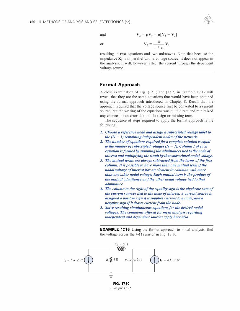
760 METHODS OF ANALYSIS AND SELECTED TOPICS (ac)
and V2 5 mVx 5 m[V1 2 V2]
or V2 5 V1
resulting in two equations and two unknowns. Note that because the
impedance Z3 is in parallel with a voltage source, it does not appear in
the analysis. It will, however, affect the current through the dependent
voltage source.
Format ApproachA close examination of Eqs. (17.1) and (17.2) in Example 17.12 will
reveal that they are the same equations that would have been obtained
using the format approach introduced in Chapter 8. Recall that the
approach required that the voltage source first be converted to a current
source, but the writing of the equations was quite direct and minimized
any chances of an error due to a lost sign or missing term.
The sequence of steps required to apply the format approach is the
following:
1. Choose a reference node and assign a subscripted voltage label to
the (N 2 1) remaining independent nodes of the network.
2. The number of equations required for a complete solution is equal
to the number of subscripted voltages (N 2 1). Column 1 of each
equation is formed by summing the admittances tied to the node of
interest and multiplying the result by that subscripted nodal voltage.
3. The mutual terms are always subtracted from the terms of the first
column. It is possible to have more than one mutual term if the
nodal voltage of interest has an element in common with more
than one other nodal voltage. Each mutual term is the product of
the mutual admittance and the other nodal voltage tied to that
admittance.
4. The column to the right of the equality sign is the algebraic sum of
the current sources tied to the node of interest. A current source is
assigned a positive sign if it supplies current to a node, and a
negative sign if it draws current from the node.
5. Solve resulting simultaneous equations for the desired nodal
voltages. The comments offered for mesh analysis regarding
independent and dependent sources apply here also.
EXAMPLE 17.16 Using the format approach to nodal analysis, find
the voltage across the 4-V resistor in Fig. 17.30.
m1 1 m
NA
I2 = 4 A ∠ 0°I1 = 6 A ∠ 0° R
XL = 5 V
XC4 V 2 V
FIG. 17.30Example 17.16.
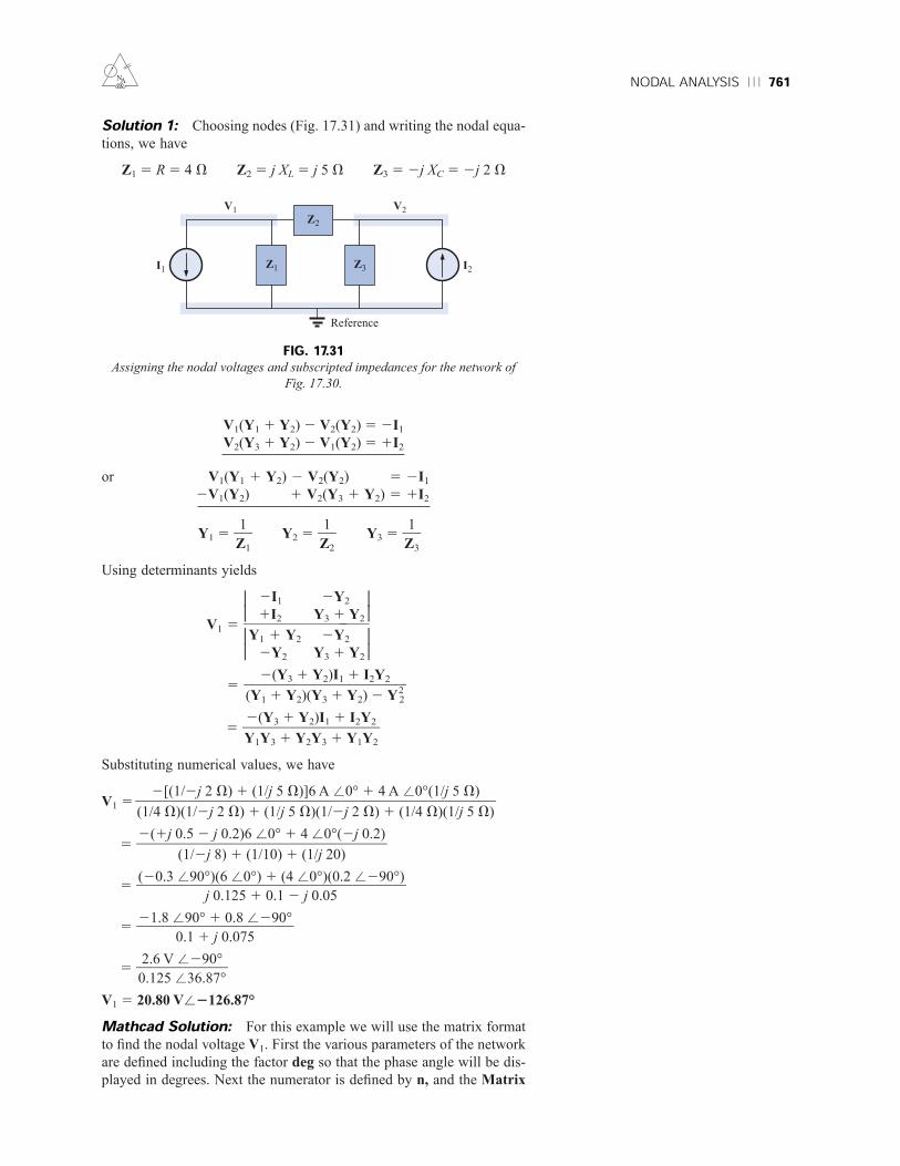
NODAL ANALYSIS 761
V1(Y1 1 Y2) 2 V2(Y2) 5 2I1
V2(Y3 1 Y2) 2 V1(Y2) 5 1I2
or V1(Y1 1 Y2) 2 V2(Y2) 5 2I1
2V1(Y2) 1 V2(Y3 1 Y2) 5 1I2
Y1 5 Y2 5 Y3 5
Using determinants yields
2I1 2Y2 1I2 Y3 1 Y2
V1 5 ––––––––––––––––––Y1 1 Y2 2Y2 2Y2 Y3 1 Y2
5
5
Substituting numerical values, we have
V1 5
5
5
5
5
V1 5 20.80 V/2126.87°
Mathcad Solution: For this example we will use the matrix format
to find the nodal voltage V1. First the various parameters of the network
are defined including the factor deg so that the phase angle will be dis-
played in degrees. Next the numerator is defined by n, and the Matrix
2.6 V /290°0.125 /36.87°
21.8 /90° 1 0.8 /290°
0.1 1 j 0.075
(20.3 /90°)(6 /0°) 1 (4 /0°)(0.2 /290°)
j 0.125 1 0.1 2 j 0.05
2(1j 0.5 2 j 0.2)6 /0° 1 4 /0°(2j 0.2)
(1/2j 8) 1 (1/10) 1 (1/j 20)
2[(1/2j 2 V) 1 (1/j 5 V)]6 A /0° 1 4 A /0°(1/j 5 V)(1/4 V)(1/2j 2 V) 1 (1/j 5 V)(1/2j 2 V) 1 (1/4 V)(1/j 5 V)
2(Y3 1 Y2)I1 1 I2Y2Y1Y3 1 Y2Y3 1 Y1Y2
2(Y3 1 Y2)I1 1 I2Y2(Y1 1 Y2)(Y3 1 Y2) 2 Y
22
1Z3
1Z2
1Z1
NA
Z1
Z2
I2
V2V1
I1Z3
Reference
FIG. 17.31Assigning the nodal voltages and subscripted impedances for the network of
Fig. 17.30.
Solution 1: Choosing nodes (Fig. 17.31) and writing the nodal equa-
tions, we have
Z1 5 R 5 4 V Z2 5 j XL 5 j 5 V Z3 5 2j XC 5 2j 2 V

762 METHODS OF ANALYSIS AND SELECTED TOPICS (ac)
icon is selected from the Matrix toolbar. Within the Insert Matrix dia-
log box, the Rows and Columns are set as 2 followed by an OK to
place the 2 3 2 matrix on the screen. The parameters are than entered
as shown in Fig. 17.32 using a left click of the mouse to select the
parameter to be entered. Once the numerator is set, the process is
repeated to define the numerator. Finally the equation for V1 is defined,
and the result in rectangular form will appear when the equal sign is
selected. The magnitude and the angle are then found in polar form as
described in earlier sections of this chapter. The results are again a clear
confirmation of the theoretical result.
NA
FIG. 17.32Using Mathcad to verify the results of Example 17.16.
EXAMPLE 17.17 Using the format approach, write the nodal equa-
tions for the network of Fig. 17.33.
I1 = 10 A ∠ 20°E1 = 20 V ∠ 0°
R2
XC = 10 V
4 V+
– XL25 V
XL1
8 V
R1
7 V
R38 V
FIG. 17.33Example 17.17.

NODAL ANALYSIS 763
Write the nodal equations:
V1(Y1 1 Y2 1 Y3) 2 V2(Y3) 5 1I2
V2(Y3 1 Y4) 2 V1(Y3) 5 1I1
Y1 5 Y2 5 Y3 5 Y4 5
which are rewritten as
V1(Y1 1 Y2 1 Y3) 2 V2(Y3) 5 1I2
2V1(Y3) 1 V2(Y3 1 Y4) 5 1I1
EXAMPLE 17.18 Write the nodal equations for the network of Fig.
17.36. Do not solve.
Solution: Choose nodes (Fig. 17.37):
Z1 5 R1 Z2 5 j XL1Z3 5 R2 2 j XC2
Z4 5 2j XC1Z5 5 R3 Z6 5 j XL2
1Z4
1Z3
1Z2
1Z1
NA
Z2
+
–
E1
Z1 Z3
I1
a
Z4
a9
FIG. 17.34Assigning the subscripted impedances for the network of Fig. 17.33.
Z1
Z3
I1
V2V1
I2 =E1
Z1
Z2
Reference
Z4
a9
a
FIG. 17.35Converting the voltage source of Fig. 17.34 to a current source and defining the
nodal voltages.
Solution: The circuit is redrawn in Fig. 17.34, where
Z1 5 R1 1 j XL15 7 V 1 j 8 V E1 5 20 V /0°
Z2 5 R2 1 j XL25 4 V 1 j 5 V I1 5 10 A /20°
Z3 5 2j XC 5 2j 10 V
Z4 5 R3 5 8 V
Converting the voltage source to a current source and choosing nodes,
we obtain Fig. 17.35. Note the “neat” appearance of the network using
the subscripted impedances. Working directly with Fig. 17.33 would be
more difficult and could produce errors.

764 METHODS OF ANALYSIS AND SELECTED TOPICS (ac) NA
R2XL2
XL1
R1I1
XC2
XC1
R3
I2
FIG. 17.36Example 17.18.
FIG. 17.37Assigning the nodal voltages and subscripted impedances for the network of
Fig. 17.36.
Z1
Z2
V2V1
I1 Z3 Z5 Z6
Z4
V3
I2
and write the nodal equations:
V1(Y1 1 Y2) 2 V2(Y2) 5 1I1
V2(Y2 1 Y3 1 Y4) 2 V1(Y2) 2 V3(Y4) 5 2I2
V3(Y4 1 Y5 1 Y6) 2 V2(Y4) 5 1I2
which are rewritten as
V1(Y1 1 Y2) 2 V2(Y2) 1 0 5 1I1
2V1(Y2) 1 V2(Y2 1 Y3 1 Y4) 2 V3(Y4) 5 2I2
0 2 V2(Y4) 1 V3(Y4 1 Y5 1 Y6) 5 1I2
Y1 5 Y2 5 Y3 5
Y4 5 Y5 5 Y6 5
Note the symmetry about the diagonal for this example and those
preceding it in this section.
1j XL2
1R3
12j XC1
1R2 2 j XC2
1j XL1
1R1

BRIDGE NETWORKS (ac) 765
Solution: In this case there is no need for a source conversion. The
network is redrawn in Fig. 17.39 with the chosen nodal voltage and
subscripted impedances.
Apply the format approach:
Y1 5 5 5 0.25 mS /0° 5 G1 /0°
Y2 5 5 5 1 mS /0° 5 G2 /0°
Y3 5 5 5 0.5 mS /290°
5 2j 0.5 mS 5 2j BL
V1: (Y1 1 Y2 1 Y3)V1 5 2100I
and V1 5
5
5 5
5 274.28 3 103I /21.80°
5 274.28 3 1031 2 /21.80°
V1 5 VL 5 2(74.28Vi) V/21.80°
17.6 BRIDGE NETWORKS (ac)The basic bridge configuration was discussed in some detail in Section
8.11 for dc networks. We now continue to examine bridge networks by
considering those that have reactive components and a sinusoidal ac
voltage or current applied.
We will first analyze various familiar forms of the bridge network
using mesh analysis and nodal analysis (the format approach). The bal-
ance conditions will be investigated throughout the section.
Vi1 kV
2100 3 103I
1.3463 /221.80°
2100 3 103I
1.25 2 j 0.5
2100I0.25 mS 1 1 mS 2 j 0.5 mS
2100IY1 1 Y2 1 Y3
12 kV /90°
1Z3
11 kV
1Z2
14 kV
1Z1
NA
Vi = Vi ∠ 0°
+
–
2 kV VLRC
100I1 kV
IB
E E
C
+
–
4 kV RL 1 kV
Transistorequivalentnetwork
XL
IL
( I)β
FIG. 17.38Example 17.19.
Y1
IL
V1
Y3 VL100I Y2
+
–
FIG. 17.39Assigning the nodal voltage and subscripted
impedances for the network of Fig. 17.38.
EXAMPLE 17.19 Apply nodal analysis to the network of Fig. 17.38.
Determine the voltage VL.

766 METHODS OF ANALYSIS AND SELECTED TOPICS (ac)
Applying the format approach:
(Z1 1 Z3)I1 2 (Z1)I2 2 (Z3)I3 5 E
(Z1 1 Z2 1 Z5)I2 2 (Z1)I1 2 (Z5)I3 5 0
(Z3 1 Z4 1 Z5)I3 2 (Z3)I1 2 (Z5)I2 5 0
which are rewritten as
I1(Z1 1 Z3) 2 I2Z1 2 I3Z3 5 E
2I1Z1 1 I2(Z1 1 Z2 1 Z5) 2 I3Z5 5 0
2I1Z3 2 I2Z5 1 I3(Z3 1 Z4 1 Z5) 5 0
Note the symmetry about the diagonal of the above equations. For
balance, IZ55 0 A, and
IZ55 I2 2 I3 5 0
From the above equations,
Z1 1 Z3 E 2Z3 2Z1 0 2Z5 2Z3 0 (Z3 1 Z4 1 Z5)
I2 5 –––––––––––––––––––––––––––––––––––––––Z1 1 Z3 2Z1 2Z3 2Z1 (Z1 1 Z2 1 Z5) 2Z5 2Z3 2Z5 (Z3 1 Z4 1 Z5)
5
where D signifies the determinant of the denominator (or coefficients).
Similarly,
I3 5
and IZ55 I2 2 I3 5
E(Z1Z4 2 Z3Z2)
D
E(Z1Z3 1 Z3Z2 1 Z1Z5 1 Z3Z5)
D
E(Z1Z3 1 Z1Z4 1 Z1Z5 1 Z3Z5)
D
NA
I1
–
Z5
Z1
Z4
Z2
Z3
+
–
E
I2
I3
FIG. 17.41Assigning the mesh currents and subscripted impedances for the network of
Fig. 17.40.
R1
+
–
E
C1
R2
R5
R3
R4
L4
FIG. 17.40Maxwell bridge.
Apply mesh analysis to the network of Fig. 17.40. The network is
redrawn in Fig. 17.41, where
Z1 5 5 5 2 j
Z2 5 R2 Z3 5 R3 Z4 5 R4 1 j XL Z5 5 R5
BCG2
1 1 B2C
G1G2
1 1 B2C
1G1 1j BC
1Y1
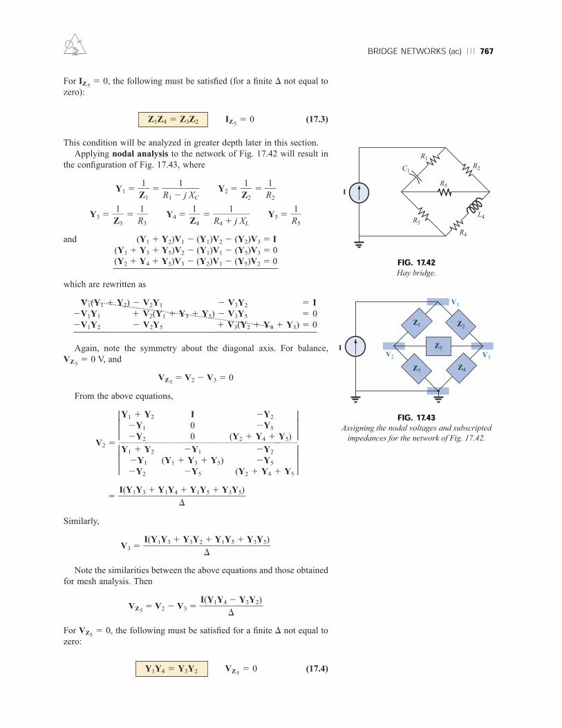
BRIDGE NETWORKS (ac) 767
For IZ55 0, the following must be satisfied (for a finite D not equal to
zero):
IZ55 0 (17.3)
This condition will be analyzed in greater depth later in this section.
Applying nodal analysis to the network of Fig. 17.42 will result in
the configuration of Fig. 17.43, where
Y1 5 5 Y2 5 5
Y3 5 5 Y4 5 5 Y5 5
and (Y1 1 Y2)V1 2 (Y1)V2 2 (Y2)V3 5 I
(Y1 1 Y3 1 Y5)V2 2 (Y1)V1 2 (Y5)V3 5 0
(Y2 1 Y4 1 Y5)V3 2 (Y2)V1 2 (Y5)V2 5 0
which are rewritten as
V1(Y1 1 Y2) 2 V2Y1 2 V3Y2 5 I
2V1Y1 1 V2(Y1 1 Y3 1 Y5) 2 V3Y5 5 0
2V1Y2 2 V2Y5 1 V3(Y2 1 Y4 1 Y5) 5 0
Again, note the symmetry about the diagonal axis. For balance,
VZ55 0 V, and
VZ55 V2 2 V3 5 0
From the above equations,
Y1 1 Y2 I 2Y2 2Y1 0 2Y5 2Y2 0 (Y2 1 Y4 1 Y5)
V2 5 ––––––––––––––––––––––––––––––––––––––––Y1 1 Y2 2Y1 2Y2 2Y1 (Y1 1 Y3 1 Y5) 2Y5 2Y2 2Y5 (Y2 1 Y4 1 Y5
5
Similarly,
V3 5
Note the similarities between the above equations and those obtained
for mesh analysis. Then
VZ55 V2 2 V3 5
For VZ55 0, the following must be satisfied for a finite D not equal to
zero:
VZ55 0 (17.4)Y1Y4 5 Y3Y2
I(Y1Y4 2 Y3Y2)
D
I(Y1Y3 1 Y3Y2 1 Y1Y5 1 Y3Y5)
D
I(Y1Y3 1 Y1Y4 1 Y1Y5 1 Y3Y5)
D
1R5
1R4 1 j XL
1Z4
1R3
1Z3
1R2
1Z2
1R1 2 j XC
1Z1
Z1Z4 5 Z3Z2
NA
R1
I
C1R2
R5
R3
R4
L4
V2
–
Z5
Z1
Z4
Z2
Z3
IV3
V1
FIG. 17.42Hay bridge.
FIG. 17.43Assigning the nodal voltages and subscripted
impedances for the network of Fig. 17.42.

NA768 METHODS OF ANALYSIS AND SELECTED TOPICS (ac)
However, substituting Y1 5 1/Z1, Y2 5 1/Z2, Y3 5 1/Z3, and Y4 5
1/Z4, we have
5
or VZ55 0
corresponding with Eq. (17.3) obtained earlier.
Let us now investigate the balance criteria in more detail by consid-
ering the network of Fig. 17.44, where it is specified that I and V 5 0.
Since I 5 0,
(17.5a)
and (17.5b)
In addition, for V 5 0,
(17.5c)
and (17.5d)
Substituting the preceding current relations into Eq. (17.5d), we have
I1Z3 5 I2Z4
and I2 5 I1
Substituting this relationship for I2 into Eq. (17.5c) yields
I1Z1 5 1 I12Z2
and Z1Z4 5 Z2Z3
as obtained earlier. Rearranging, we have
(17.6)
corresponding with Eq. (8.4) for dc resistive networks.
For the network of Fig. 17.42, which is referred to as a Hay bridge
when Z5 is replaced by a sensitive galvanometer,
Z1 5 R1 2 j XC
Z2 5 R2
Z3 5 R3
Z4 5 R4 1 j XL
This particular network is used for measuring the resistance and induc-
tance of coils in which the resistance is a small fraction of the reactance
XL.
Z
Z
1
3
5 Z
Z
2
4
Z3Z4
Z3Z4
I3Z3 5 I4Z4
I1Z1 5 I2Z2
I2 5 I4
I1 5 I3
Z1Z4 5 Z3Z2
1Z3Z2
1Z1Z4
I1
–
Z1
Z4
Z2
Z3
+
–
E+
I4
I2
I3V = 0
I = 0
–
FIG. 17.44Investigating the balance criteria for an ac
bridge configuration.

BRIDGE NETWORKS (ac) 769
Substitute into Eq. (17.6) in the following form:
Z2Z3 5 Z4Z1
R2R3 5 (R4 1 j XL)(R1 2 j XC)
or R2R3 5 R1R4 1 j (R1XL 2 R4XC) 1 XC XL
so that
R2R3 1 j 0 5 (R1R4 1 XC XL) 1 j (R1XL 2 R4XC)
For the equations to be equal, the real and imaginary parts must be
equal. Therefore, for a balanced Hay bridge,
(17.7a)
and (17.7b)
or substituting XL 5 qL and XC 5
we have XC XL 5 1 2(qL) 5
and R2R3 5 R1R4 1
with R1qL 5
Solving for R4 in the last equation yields
R4 5 q2LCR1
and substituting into the previous equation, we have
R2R3 5 R1(q2LCR1) 1
Multiply through by C and factor:
CR2R3 5 L(q2C2R21 1 1)
and (17.8a)
With additional algebra this yields:
(17.8b)
Equations (17.7) and (17.8) are the balance conditions for the Hay
bridge. Note that each is frequency dependent. For different frequen-
cies, the resistive and capacitive elements must vary for a particular coil
to achieve balance. For a coil placed in the Hay bridge as shown in Fig.
17.42, the resistance and inductance of the coil can be determined by
Eqs. (17.8a) and (17.8b) when balance is achieved.
R4 5 1
q2
1
C2
q
R21
C
R22
R
R
321
L 5 1 1
CR
q
2
2
R
C
3
2R21
LC
R4qC
LC
LC
1qC
1qC
0 5 R1XL 2 R4XC
R2R3 5 R1R4 1 XC XL
NA

770 METHODS OF ANALYSIS AND SELECTED TOPICS (ac)
The bridge of Fig. 17.40 is referred to as a Maxwell bridge when Z5
is replaced by a sensitive galvanometer. This setup is used for induc-
tance measurements when the resistance of the coil is large enough not
to require a Hay bridge.
Application of Eq. (17.6) in the form:
Z2Z3 5 Z4Z1
and substituting
Z1 5 R1 /0° \ XC1/290° 5
5 5
Z2 5 R2
Z3 5 R3
and Z4 5 R4 1 j XL4
we have (R2)(R3) 5 (R4 1 j XL4)1 2
R2R3 5
or (R2R3)(R1 2 j XC1) 5 R1XC1
XL42 j R1R4XC1
and R1R2R32 j R2R3XC15 R1XC1
XL42 j R1R4XC1
so that for balance
R1R2R3 5 R1XC1XL4
R2R3 5 1 2(2 pf L4)
and (17.9)
and R2R3XC15 R1R4XC1
so that (17.10)
Note the absence of frequency in Eqs. (17.9) and (17.10).
One remaining popular bridge is the capacitance comparison
bridge of Fig. 17.45. An unknown capacitance and its associated resis-
tance can be determined using this bridge. Application of Eq. (17.6)
will yield the following results:
(17.11)
(17.12)
The derivation of these equations will appear as a problem at the end of
the chapter.
R4 5 R
R
2R
1
3
C4 5 C3R
R
1
2
R4 5 R
R
2R
1
3
L4 5 C1R2R3
12pfC
1
2j R1R4XC11 R1XC1
XL4
R12j XC1
2j R1XC1R1 2j XC1
2j R1XC1R1 2j XC1
R1XC1/290°
R1 2 j XC1
(R1 /0°)(XC1/290°)
R1 2 j XC1
NA
R1
E
C3
R2
Galvanometer
R3 R4
C4
+
–
FIG. 17.45Capacitance comparison bridge.

D-Y, Y-D CONVERSIONS 771NA
ZC
Z3
Z1 Z2
ZB ZA
a b
c
FIG. 17.46D-Y configuration.
Z3
Z1 Z2
ZB ZA
ZC
FIG. 17.47The T and p configurations.
17.7 D-Y, Y-D CONVERSIONSThe D-Y, Y-D (or p-T, T-p as defined in Section 8.12) conversions for
ac circuits will not be derived here since the development corresponds
exactly with that for dc circuits. Taking the D-Y configuration shown
in Fig. 17.46, we find the general equations for the impedances of the Y
in terms of those for the D:
(17.13)
(17.14)
(17.15)
For the impedances of the D in terms of those for the Y, the equations are
ZB 5 (17.16)
ZA 5 (17.17)
ZC 5 (17.18)
Note that each impedance of the Y is equal to the product of the
impedances in the two closest branches of the D, divided by the sum
of the impedances in the D.
Further, the value of each impedance of the D is equal to the sum of the
possible product combinations of the impedances of theY, divided by the
impedances of theY farthest from the impedance to be determined.
Drawn in different forms (Fig. 17.47), they are also referred to as the T
and p configurations.
Z1Z2 1 Z1Z3 1 Z2Z3
Z3
Z1Z2 1 Z1Z3 1 Z2Z3
Z1
Z1Z2 1 Z1Z3 1 Z2Z3
Z2
Z3 5 ZA 1
Z
Z
AZ
B
B
1 ZC
Z2 5 ZA 1
Z
Z
AZ
B
C
1 ZC
Z1 5 ZA 1
Z
Z
BZ
B
C
1 ZC

772 METHODS OF ANALYSIS AND SELECTED TOPICS (ac)
In the study of dc networks, we found that if all of the resistors of
the D or Y were the same, the conversion from one to the other could
be accomplished using the equation
RD 5 3RY or RY 5
For ac networks,
(17.19)
Be careful when using this simplified form. It is not sufficient for all the
impedances of the D or Y to be of the same magnitude: The angle asso-
ciated with each must also be the same.
EXAMPLE 17.20 Find the total impedance ZT of the network of Fig.
17.48.
ZD 5 3ZY or ZY 5 Z
3
D
RD3
NA
4 V
ZT
4 V
3 V 4 V
2 V 3 V
1 3
2
ZC1 3
2
ZB ZA
1 3
2
Z1
Z3
Z2
FIG. 17.48Converting the upper D of a bridge configuration to a Y.
Solution:ZB 5 2j 4 ZA 5 2j 4 ZC 5 3 1 j 4
Z1 5 5
5 5
5 4 V /16.13° 5 3.84 V 1 j 1.11 V
Z2 5 5
5 4 V /16.13° 5 3.84 V 1 j 1.11 V
Recall from the study of dc circuits that if two branches of the Y or D
were the same, the corresponding D or Y, respectively, would also have
(2j 4 V)(3 V 1 j 4 V)
5 V /253.13°
ZAZCZA 1 ZB 1 ZC
20 /236.87°5 /253.13°
(4 /290°)(5 /53.13°)
3 2 j 4
(2j 4 V)(3 V 1 j 4 V)(2j 4 V) 1 (2j 4 V) 1 (3 V 1 j 4 V)
ZBZCZA 1 ZB 1 ZC

D-Y, Y-D CONVERSIONS 773
two similar branches. In this example, ZA 5 ZB. Therefore, Z1 5 Z2,
and
Z3 5 5
5 5 3.2 V /2126.87° 5 21.92 V 2 j 2.56 V
Replace the D by the Y (Fig. 17.49):
Z1 5 3.84 V 1 j 1.11 V Z2 5 3.84 V 1 j 1.11 V
Z3 5 21.92 V 2 j 2.56 V Z4 5 2 V
Z5 5 3 V
Impedances Z1 and Z4 are in series:
ZT15 Z1 1 Z4 5 3.84 V 1 j 1.11 V 1 2 V 5 5.84 V 1 j 1.11 V
5 5.94 V /10.76°
Impedances Z2 and Z5 are in series:
ZT25 Z2 1 Z5 5 3.84 V 1 j 1.11 V 1 3 V 5 6.84 V 1 j 1.11 V
5 6.93 V /9.22°
Impedances ZT1and ZT2
are in parallel:
ZT35 5
5 5 5 3.198 V /10.05°
5 3.15 V 1 j 0.56 V
Impedances Z3 and ZT3are in series. Therefore,
ZT 5 Z3 1 ZT3
5 21.92 V 2 j 2.56 V 1 3.15 V 1 j 0.56 V
5 1.23 V 2 j 2.0 V 5 2.35 V /258.41°
EXAMPLE 17.21 Using both the D-Y and Y-D transformations, find
the total impedance ZT for the network of Fig. 17.50.
41.16 V /19.98°
12.87 /9.93°
41.16 V /19.98°
12.68 1 j 2.22
(5.94 V /10.76°)(6.93 V /9.22°)5.84 V 1 j 1.11 V 1 6.84 V 1 j 1.11 V
ZT1ZT2
ZT1
1 ZT2
16 V /2180°
5 /253.13°
(2j 4 V)(2j 4 V)
5 V /253.13°
ZAZBZA 1 ZB 1 ZC
NA
Z3
2
ZT
Z1 Z2
Z5Z4
1 3
FIG. 17.49The network of Fig. 17.48 following the
substitution of the Y configuration.
6 V
ZT 3 V
2 V
2 V
3 V1 3
2
6 V
3 V
1 V
2 V 1 V1 V
6 V d
FIG. 17.50Example 17.21.
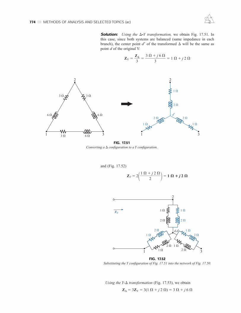
774 METHODS OF ANALYSIS AND SELECTED TOPICS (ac)
Solution: Using the D-Y transformation, we obtain Fig. 17.51. In
this case, since both systems are balanced (same impedance in each
branch), the center point d ′ of the transformed D will be the same as
point d of the original Y:
ZY 5 5 5 1 V 1 j 2 V3 V 1 j 6 V
3
ZD3
NA
ZT
1 3
2
d,d9
2 V
1 V
2 V
1 V
1 V
1 V
2 V
2 V
1 V
1 V
2 V
2 V
FIG. 17.52Substituting the Y configuration of Fig. 17.51 into the network of Fig. 17.50.
and (Fig. 17.52)
ZT 5 21 2 5 1 V 1 j 2 V1 V 1 j 2 V
2
Using the Y-D transformation (Fig. 17.53), we obtain
Z∆ 5 3ZY 5 3(1 V 1 j 2 V) 5 3 V 1 j 6 V
6 V
3 V
2 V
2 V
3 V1 3
2
6 V
3 V
1 V
2 V
1 V1 V
6 V d9
1 3
2
FIG. 17.51Converting a D configuration to a Y configuration.

COMPUTER ANALYSIS 775
Each resulting parallel combination in Fig. 17.54 will have the fol-
lowing impedance:
Z′ 5 5 1.5 V 1 j 3 V3 V 1 j 6 V
2
NA
6 V
3 V
3 V1 3
2
6 V
3 V
6 V
2 V
2 V
1 V
2 V
1 V1 V
d
1 3
2
FIG. 17.53Converting the Y configuration of Fig. 17.50 to a D.
6 V
ZT
3 V
1 3
2
6 V3 V
6 V 6 V
3 V
3 V
6 V
3 V
6 V3 V
FIG. 17.54Substituting the D configuration of Fig. 17.53 into the network of Fig. 17.50.
and ZT 5 5 5
5 5 1 V 1 j 2 V
which compares with the above result.
17.8 COMPUTER ANALYSISPSpiceNodal Analysis The first application of PSpice will be to determine
the nodal voltages for the network of Example 17.16 and compare solu-
tions. The network will appear as shown in Fig. 17.55 using elements
2(1.5 V 1 j 3 V)
3
2Z′
3
2(Z′)2
3Z′
Z′(2Z′)Z′ 1 2Z′

776 METHODS OF ANALYSIS AND SELECTED TOPICS (ac)
that were determined from the reactance level at a frequency of 1 kHz.
There is no need to continually use 1 kHz. Any frequency will do, but
remember to use the chosen frequency to find the network components
and when setting up the simulation.
For the current sources, ISIN was chosen so that the phase angle
could be specified (even though it is 0°), although the symbol does not
have the arrow used in the text material. The direction must be recog-
nized as pointing from the 1 to 2 sign of the source. That requires that
the sources I1 and I2 be set as shown in Fig. 17.55. The source I2 is
reversed by using the Mirror Vertically option obtained by right-
clicking the source symbol on the screen. Setting up the ISIN source is
the same as that employed with the VSIN source. It can be found under
the SOURCE library, and its attributes are the same as for the VSIN
source. For each source, IOFF is set to 0 A, and the amplitude is the
peak value of the source current. The frequency will be the same for
each source. Then VPRINT1 is selected from the SPECIAL library
and placed to generate the desired nodal voltages. Finally the remaining
elements are added to the network as shown in Fig. 17.55. For each
source the symbol is double-clicked to generate the Property Editor
dialog box. AC is set at the 6-A level for the I1 source and at 4 A for
the I2 source, followed by Display and Name and Value for each. It
will appear as shown in Fig. 17.55. A double-click on each VPRINT1
option will also provide the Property Editor, so OK can be added
under AC, MAG, and PHASE. For each quantity, Display is selected
followed by Name and Value and OK. Then Value is selected and
VPRINT1 is displayed as Value only. Selecting Apply and leaving the
dialog box will result in the listing next to each source in Fig. 17.55.
For VPRINT2 the listing on Value must first be changed from
VPRINT1 to VPRINT2 before selecting Display and Apply.
NA
FIG. 17.55Using PSpice to verify the results of Example 17.16.

COMPUTER ANALYSIS 777
Now the New Simulation Profile icon is selected and ACNodal
entered as the Name followed by Create. In the Simulation Settings
dialog box, AC Sweep is selected, and the Start Frequency and End
Frequency are set at 1 kHz with 1 for the Points/Decade. Click OK,
and select the Run PSpice icon; a SCHEMATIC1 screen will result.
Exiting (X) will bring us back to the Orcad Capture window. Select-
ing PSpice followed by View Output File will result in the display of
Fig. 17.56, providing exactly the same results as obtained in Example
17.16 with V1 5 20.8 V /2126.9°. The other nodal voltage is 8.617 V
/215.09°.
NA
FIG. 17.56Output file for the nodal voltages for the network of Fig. 17.55.
Current-Controlled Current Source (CCCS) Our interest will
now turn to controlled sources in the PSpice environment. Controlled
sources are not particularly difficult to apply once a few important ele-
ments of their use are understood. The network of Fig. 17.14 has a
current-controlled current source in the center leg of the configuration.
The magnitude of the current source is k times the current through resis-
tor R1, where k can be greater or less than 1. The resulting schematic,
appearing in Fig. 17.57, seems quite complex in the area of the con-
trolled source, but once the role of each component is understood, it
will not be that difficult to understand. First, since it is the only new
element in the schematic, let us concentrate on the controlled source.
Current-controlled current sources (CCCS) are called up under the
ANALOG library as F and appear as shown in the center of Fig. 17.57.

778 METHODS OF ANALYSIS AND SELECTED TOPICS (ac) NA
Take special note of the direction of the current in each part of the sym-
bol. In particular, note that the sensing current of F has the same direc-
tion as the defining controlling current in Fig. 17.14. In addition, note
that the controlled current source also has the same direction as the
source in Fig. 17.14. If we double-click on the CCCS symbol, the
Property Editor dialog box will appear with the GAIN (k as described
above) set at 1. In this example the gain must be set at 0.7, so click on
the region below the GAIN label and enter 0.7. Then select Display
followed by Name and Value-OK. Exit the Property Editor, and
GAIN 5 0.7 will appear with the CCCS as shown in Fig. 17.57.
The other new component in this schematic is IPRINT; it can be
found in the SPECIAL library. It is used to tell the program to list the
current in the branch of interest in the output file. If you fail to tell the
program which output data you would like, it will simply run through
the simulation and list specific features of the network but will not pro-
vide any voltages or currents. In this case the current I2 through the
resistor R2 is desired. Double-clicking on the IPRINT component will
result in the Property Editor dialog box with a number of elements
that need to be defined—much like that for VPRINT. First enter OK
beneath AC and follow with Display-Name and Value-OK. Repeat for
MAG and PHASE, and then select Apply before leaving the dialog
box. The OK is designed simply to tell the software program that these
are the quantities that it is “ok” to generate and provide. The purpose of
the Apply at the end of each visit to the Property Editor dialog box is
to “apply” the changes made to the network under investigation. When
you exit the Property Editor, the three chosen parameters will appear
on the schematic with the OK directive. You may find that the labels
FIG. 17.57Using PSpice to verify the results of Example 17.8.

COMPUTER ANALYSIS 779
will appear all over the IPRINT symbol. No problem—just click on
each, and move to a more convenient location.
The remaining components of the network should be fairly familiar,
but don’t forget to Mirror Vertically the voltage source E2. In addi-
tion, do not forget to call up the Property Editor for each source and
set the level of AC, FREQ, VAMPL, and VOFF and be sure that the
PHASE is set on the default value of 0°. The value appears with each
parameter in Fig. 17.57 for each source. Always be sure to select Apply
before leaving the Property Editor. After placing all the components
on the screen, you must connect them with a Place wire selection. Nor-
mally, this is pretty straightforward. However, with controlled sources
there is often the need to cross over wires without making a connec-
tion. In general, when you’re placing a wire over another wire and you
don’t want a connection to be made, click a spot on one side of the wire
to be crossed to create the temporary red square. Then cross the wire,
and make another click to establish another red square. If the connec-
tion is done properly, the crossed wire should not show a connection
point (a small red dot). In this example the top of the controlling cur-
rent was connected first from the E1 source. Then a wire was connected
from the lower end of the sensing current to the point where a 90° turn
up the page was to be made. The wire was clicked in place at this point
before crossing the original wire and clicked again before making the
right turn to resistor R1. You will not find a small red dot where the
wires cross.
Now for the simulation. In the Simulation Settings dialog box,
select AC Sweep/Noise with a Start and End Frequency of 1 kHz.
There will be 1 Point/Decade. Click OK, and select the Run Spice
key; a SCHEMATIC1 will result that should be exited to obtain the
Orcad Capture screen. Select PSpice followed by View Output File,
and scroll down until you read AC ANALYSIS such as appearing in
Fig. 17.58. The magnitude of the desired current is 1.615 mA with a
phase angle of 0°, a perfect match with the theoretical analysis to fol-
low. One would expect a phase angle of 0° since the network is com-
posed solely of resistive elements.
The equations obtained earlier using the supermesh approach were
E 2 I1Z1 2 I2Z2 1 E2 5 0 or I1Z1 1 I2Z2 5 E1 1 E2
NA
FIG. 17.58The output file for the mesh current I2 of Fig. 17.14.

3. Convert the current sources of Fig. 17.60 to voltage
sources.
780 METHODS OF ANALYSIS AND SELECTED TOPICS (ac) NA
and kI 5 kI1 5 I1 2 I2
resulting in I1 5 5 5 5 3.333I2
so that I1(1 kV) 1 I2(1 kV) 5 7 V (from above)
becomes (3.333I2)1 kV 1 I2 (1 kV) 5 7 V
or (4.333 kV)I2 5 7 V
and I2 5 5 1.615 mA /0°
confirming the computer solution.
7 V4.333 kV
I20.3
I21 2 0.7
I21 2 k
5.6 V
E = 20 V ∠ 20°
8.2 V
(a)
2 V
E = 60 V ∠ 30°5 V
(b)
+
–
+
–
FIG. 17.59Problem 2.
(a) (b)
6 V 2 A / 120°10 V I
15 V
16 V
I = 0.5 A / 60°
FIG. 17.60Problem 3.
PROBLEMSSECTION 17.2 Independent versus Dependent(Controlled) Sources
1. Discuss, in your own words, the difference between a con-
trolled and an independent source.
SECTION 17.3 Source Conversions2. Convert the voltage sources of Fig. 17.59 to current
sources.

PROBLEMS 781NA
(a) (b)
R
4 kV
+
–V
+
–hI R 50 kVI
(h = 50)
Vm
(m = 16)m
FIG. 17.61Problem 4.
4. Convert the voltage source of Fig. 17.61(a) to a current
source and the current source of Fig. 17.61(b) to a volt-
age source.
+
E1 = 10 V ∠ 0°–
R
4 V 8 V
6 V
+
–
E2 = 40 V ∠ 60°
(b)(a)
+
–
R 50 V 20 V
E1 = 5 V ∠ 30°+
–E2 20 V ∠ 0°
60 V
FIG. 17.62Problems 5 and 34.
+E1 =
20 V ∠ 50°–
R1
12 V1 V
E3 = 40 V ∠ 0°
(a)
12 V 3 V
E2
+
–
+
–
60 V ∠ 70°
(b)
20 V10 V
E = 30 V ∠ 0°
10 V2 V +
–
20 V
I =6 A ∠ 0°
R1
FIG. 17.63Problems 6 and 16.
SECTION 17.4 Mesh Analysis5. Write the mesh equations for the networks of Fig. 17.62.
Determine the current through the resistor R.
6. Write the mesh equations for the networks of Fig. 17.63.
Determine the current through the resistor R1.

9. Using mesh analysis, determine the current IL (in terms
of V) for the network of Fig. 17.66.
782 METHODS OF ANALYSIS AND SELECTED TOPICS (ac) NA
*7. Write the mesh equations for the networks of Fig. 17.64.
Determine the current through the resistor R1.
R1
6 V
E1 = 20 V ∠ 0°
8 V
5 V 4 V
5 V
6 V 4 V
+
–
+
–
E2 = 40 V ∠ 60°
(a)
5 V
E1 = 25 V ∠ 0°
5 V
20 V
15 V+
–
(b)
R1
10 V
+
–E2 = 75 V ∠ 20°
6 V
20 V
10 V 20 V
80 V
FIG. 17.65Problems 8, 18, and 19.
XL 4 kV
+
–28 V
+
–
5 kV
10 kV
rp
Rp
1 kVRL
VL
IL
+
–V
FIG. 17.66Problem 9.
3 V
(b)
10 V
15 V+
–
4 V
R1
+
E1 = 60 V ∠ 0°–
4 V
(a)
3 V
1 V
+
–
E2 = 120 V ∠ 120°
R1
8 V
6 V
2 V
+
–
E1 = 220 V ∠ 0° E2 = 100 V ∠ 90°
15 V
FIG. 17.64Problems 7, 17, and 35.
*8. Write the mesh equations for the networks of Fig. 17.65.
Determine the current through the resistor R1.

PROBLEMS 783NA
XL 4 kV
+
–
50I 40 kV
0.2 kV
R VL
I
XC
R1 8 kV
IL
FIG. 17.67Problem 10.
10 V∠ 0° 2 kV Vx
+
–
1 kV
6 Vx
+
–
4 kV+
–
FIG. 17.68Problems 11 and 36.
5 V∠ 0° 10 kV
2.2 kV
5 kV
+
–
4 mA ∠ 0°
+20 V∠ 0°
–
FIG. 17.69Problems 12 and 37.
*11. Write the mesh equations for the network of Fig. 17.68,
and determine the current through the 1-kV and 2-kV
resistors.
6 mA ∠ 0° 6 kV
4 kV
1 kV
+
–
0.1 Vs
+10 V ∠ 0°
–
Vs
FIG. 17.70Problems 13 and 38.
*13. Write the mesh equations for the network of Fig. 17.70,
and determine the current through the inductive element.
*10. Using mesh analysis, determine the current IL (in terms
of I) for the network of Fig. 17.67.
*12. Write the mesh equations for the network of Fig. 17.69,
and determine the current through the 10-kV resistor.
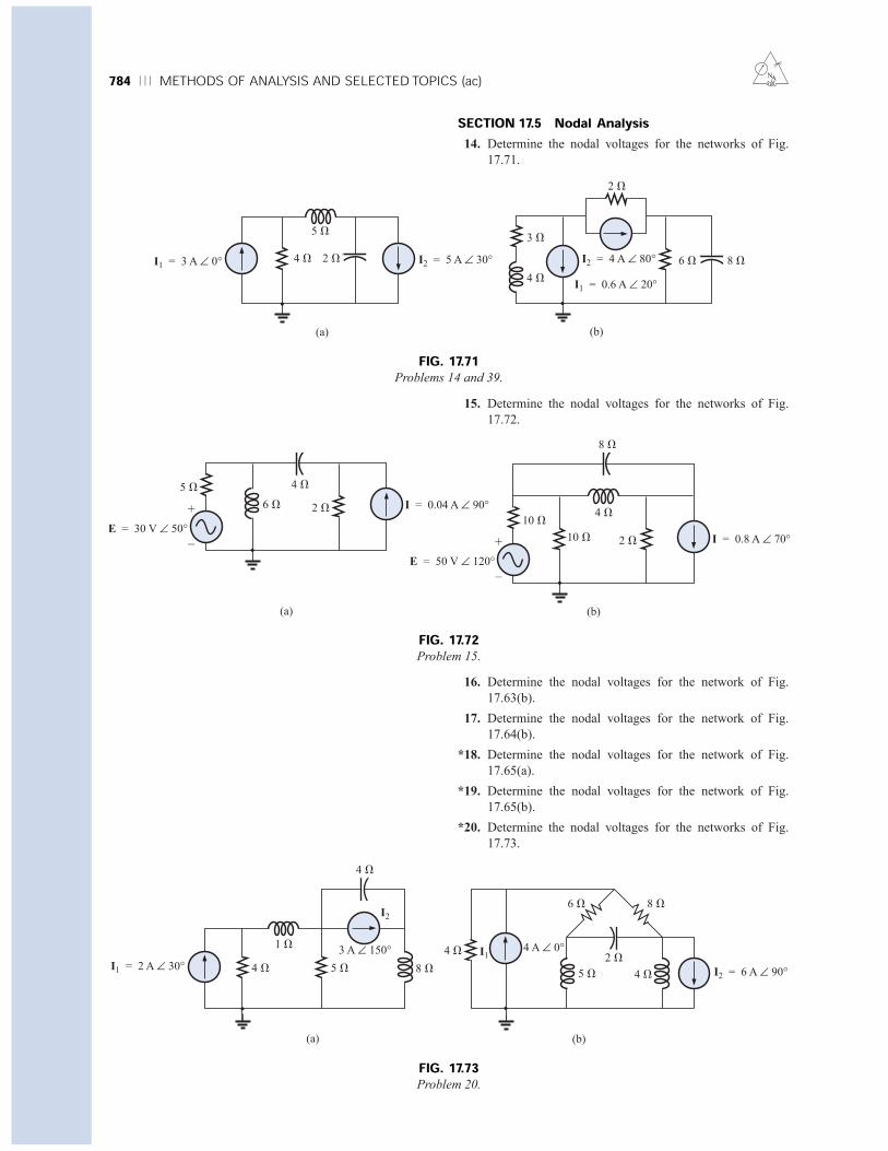
SECTION 17.5 Nodal Analysis14. Determine the nodal voltages for the networks of Fig.
17.71.
784 METHODS OF ANALYSIS AND SELECTED TOPICS (ac) NA
I2
5 V
3 A ∠ 150°4 V
1 V
8 V
4 V
I1 = 2 A ∠ 30°
(a)
6 V
I2 = 6 A ∠ 90°
4 V
5 V 4 V
4 A ∠ 0°
(b)
8 V
2 VI1
FIG. 17.73Problem 20.
15. Determine the nodal voltages for the networks of Fig.
17.72.
16. Determine the nodal voltages for the network of Fig.
17.63(b).
17. Determine the nodal voltages for the network of Fig.
17.64(b).
*18. Determine the nodal voltages for the network of Fig.
17.65(a).
*19. Determine the nodal voltages for the network of Fig.
17.65(b).
*20. Determine the nodal voltages for the networks of Fig.
17.73.
I1 = 3 A ∠ 0° 4 V
5 V
(a)
I2 = 5 A ∠ 30°
2 V
(b)
I2 = 4 A ∠ 80°
3 V
2 V
4 V
6 V 8 V
I1 = 0.6 A ∠ 20°
FIG. 17.71Problems 14 and 39.
4 V+
–
E = 30 V ∠ 50°
6 V
4 V
2 V
5 V
(a)
I = 0.04 A ∠ 90°
+
–
E = 50 V ∠ 120°
10 V
8 V
2 V
(b)
I = 0.8 A ∠ 70°10 V
FIG. 17.72Problem 15.

PROBLEMS 785NA
5 mA ∠ 0°
2 kV
1 kV
Ix
8 mA ∠ 0°4 kV
4Ix
FIG. 17.74Problems 21 and 40.
12 mA ∠ 0°
2 kV
1 kV 4 mA ∠ 0°3 kV
10 V ∠ 0°+–
FIG. 17.75Problems 22 and 41.
*21. Write the nodal equations for the network of Fig. 17.74,
and find the voltage across the 1-kV resistor.
12 mA ∠ 0°
1 kV
2 kV
2 mA ∠ 0°
+ –Vx
3.3 kV
6Vx
+
–
FIG. 17.76Problems 23 and 42.
5 mA ∠ 0°
1 kV
2 kV
+–
I1
1 kV
2Vx
Vx
+
–
3I1
FIG. 17.77Problems 24 and 43.
*22. Write the nodal equations for the network of Fig. 17.75,
and find the voltage across the capacitive element.
*23. Write the nodal equations for the network of Fig. 17.76,
and find the voltage across the 2-kV resistor.
*24. Write the nodal equations for the network of Fig. 17.77,
and find the voltage across the 2-kV resistor.

R1
1 kV
E
+
–
Lx
0.1 kV
1 mF IG = 0
CRs 1 kVR2
R3
q = 1000
Rx
0.1 kV
FIG. 17.81Problem 28.
R1
4 kV
Es = 10 V ∠ 0°
+
–
XL
4 kV 4 kV
4 kVXC
Rs 1 kVR2
4 kVR3
FIG. 17.80Problem 27.
*25. For the network of Fig. 17.78, determine the voltage VL
in terms of the voltage Ei.
786 METHODS OF ANALYSIS AND SELECTED TOPICS (ac) NA
SECTION 17.6 Bridge Networks (ac)26. For the bridge network of Fig. 17.79:
a. Is the bridge balanced?
b. Using mesh analysis, determine the current through
the capacitive reactance.
c. Using nodal analysis, determine the voltage across the
capacitive reactance.
27. For the bridge network of Fig. 17.80:
a. Is the bridge balanced?
b. Using mesh analysis, determine the current through
the capacitive reactance.
c. Using nodal analysis, determine the voltage across the
capacitive reactance.
28. The Hay bridge of Fig. 17.81 is balanced. Using Eq.
(17.3), determine the unknown inductance Lx and resis-
tance Rx.
R1 1 kV
I1
Ei
+
–R250 kV50I1 RL 50 kV50I2
R3
1 kV
VL
+
–
I2
FIG. 17.78Problem 25.
R1
5 kV
Es = 10 V ∠ 0°
+
–
XL1
2.5 kV
XL2
4 kV
5 kV
XC
Rs 1 kVR2
8 kV
FIG. 17.79Problem 26.

R1 = 2 kV
E
+
–Lx
4 kV
3 mF
IG
C1
R2
R3q = 1000Rx
0.5 kV
1 kV
6 H
FIG. 17.82Problem 29.
R1
E
+
–L3 Lx
Rs
R2
R3 Rx
FIG. 17.83Problem 31.
PROBLEMS 787NA
29. Determine whether the Maxwell bridge of Fig. 17.82 is
balanced (q 5 1000 rad/s).
8 V
E = 120 V ∠ 0°+
–
8 V
5 V
I
YT
ZT
4 V
6 V
(a)
9 V
E = 60 V ∠ 0°+
–9 V12 V
I
YT
ZT
12 V
3 V
(b)
3 V
12 V
2 V
9 V
FIG. 17.84Problem 32.
30. Derive the balance equations (17.11) and (17.12) for the
capacitance comparison bridge.
31. Determine the balance equations for the inductance
bridge of Fig. 17.83.
SECTION 17.7 D-Y, Y-D Conversions32. Using the D-Y or Y-D conversion, determine the current
I for the networks of Fig. 17.84.

788 METHODS OF ANALYSIS AND SELECTED TOPICS (ac) NA
SECTION 17.8 Computer AnalysisPSpice or Electronics Workbench34. Determine the mesh currents for the network of Fig.
17.62(a).
35. Determine the mesh currents for the network of Fig.
17.64(a).
*36. Determine the mesh currents for the network of Fig.
17.68.
*37. Determine the mesh currents for the network of Fig.
17.69.
*38. Determine the mesh currents for the network of Fig.
17.70.
39. Determine the nodal voltages for the network of Fig.
17.71(b).
*40. Determine the nodal voltages for the network of Fig.
17.74.
*41. Determine the nodal voltages for the network of Fig.
17.75.
*42. Determine the nodal voltages for the network of Fig.
17.76.
*43. Determine the nodal voltages for the network of Fig.
17.77.
Programming Language (C11, QBASIC, Pascal, etc.)44. Write a computer program that will provide a general
solution for the network of Fig. 17.10. That is, given the
reactance of each element and the parameters of the
source voltages, generate a solution in phasor form for
both mesh currents.
45. Repeat Problem 35 for the nodal voltages of Fig. 17.30.
46. Given a bridge composed of series impedances in each
branch, write a program to test the balance condition as
defined by Eq. (17.6).
33. Using the D-Y or Y-D conversion, determine the current
I for the networks of Fig. 17.85. (E 5 100 V /0° in each
case.)
FIG. 17.85Problem 33.
E
+
–
12 V
I
YT
ZT
16 V
(a)
3 V3 V
12 V 12 V3 V
16 V 16 V
E
+
–
I
YT
ZT
(b)
5 V
5 V
6 V
5 V 5 V
5 V

GLOSSARY 789
GLOSSARYBridge network A network configuration having the appear-
ance of a diamond in which no two branches are in series or
parallel.
Capacitance comparison bridge A bridge configuration
having a galvanometer in the bridge arm that is used to deter-
mine an unknown capacitance and associated resistance.
Delta (D) configuration A network configuration having the
appearance of the capital Greek letter delta.
Dependent (controlled) source A source whose magnitude
and/or phase angle is determined (controlled) by a current
or voltage of the system in which it appears.
Hay bridge A bridge configuration used for measuring the
resistance and inductance of coils in those cases where the
resistance is a small fraction of the reactance of the coil.
Independent source A source whose magnitude is indepen-
dent of the network to which it is applied. It displays its ter-
minal characteristics even if completely isolated.
NA
Maxwell bridge A bridge configuration used for inductance
measurements when the resistance of the coil is large
enough not to require a Hay bridge.
Mesh analysis A method through which the loop (or mesh)
currents of a network can be determined. The branch cur-
rents of the network can then be determined directly from
the loop currents.
Nodal analysis A method through which the nodal voltages
of a network can be determined. The voltage across each
element can then be determined through application of
Kirchhoff’s voltage law.
Source conversion The changing of a voltage source to a
current source, or vice versa, which will result in the same
terminal behavior of the source. In other words, the external
network is unaware of the change in sources.
Wye (Y) configuration A network configuration having the
appearance of the capital letter Y.


Network Theorems (ac)
Th18
18.1 INTRODUCTIONThis chapter will parallel Chapter 9, which dealt with network theorems
as applied to dc networks. It would be time well spent to review each
theorem in Chapter 9 before beginning this chapter because many of the
comments offered there will not be repeated.
Due to the need for developing confidence in the application of the
various theorems to networks with controlled (dependent) sources,
some sections have been divided into two parts: independent sources
and dependent sources.
Theorems to be considered in detail include the superposition theo-
rem, Thévenin’s and Norton’s theorems, and the maximum power theo-
rem. The substitution and reciprocity theorems and Millman’s theorem
are not discussed in detail here because a review of Chapter 9 will
enable you to apply them to sinusoidal ac networks with little difficulty.
18.2 SUPERPOSITION THEOREMYou will recall from Chapter 9 that the superposition theorem elimi-
nated the need for solving simultaneous linear equations by considering
the effects of each source independently. To consider the effects of each
source, we had to remove the remaining sources. This was accom-
plished by setting voltage sources to zero (short-circuit representation)
and current sources to zero (open-circuit representation). The current
through, or voltage across, a portion of the network produced by each
source was then added algebraically to find the total solution for the
current or voltage.
The only variation in applying this method to ac networks with inde-
pendent sources is that we will now be working with impedances and
phasors instead of just resistors and real numbers.
The superposition theorem is not applicable to power effects in ac
networks since we are still dealing with a nonlinear relationship. It can
be applied to networks with sources of different frequencies only if

792 NETWORK THEOREMS (ac)
the total response for each frequency is found independently and the
results are expanded in a nonsinusoidal expression, as appearing in
Chapter 25.
One of the most frequent applications of the superposition theorem
is to electronic systems in which the dc and ac analyses are treated sep-
arately and the total solution is the sum of the two. It is an important
application of the theorem because the impact of the reactive elements
changes dramatically in response to the two types of independent
sources. In addition, the dc analysis of an electronic system can often
define important parameters for the ac analysis. Example 18.4 will
demonstrate the impact of the applied source on the general configura-
tion of the network.
We will first consider networks with only independent sources to
provide a close association with the analysis of Chapter 9.
Independent Sources
EXAMPLE 18.1 Using the superposition theorem, find the current I
through the 4-V reactance (XL2) of Fig. 18.1.
Th
XL24 V
–
+
XC 3 VI
E2 = 5 V ∠ 0°E1 = 10 V ∠ 0°
–
+
XL14 V
FIG. 18.1Example 18.1.
Solution: For the redrawn circuit (Fig. 18.2),
Z1 5 1j XL15 j 4 V
Z2 5 1j XL25 j 4 V
Z3 5 2j XC 5 2j 3 V
Considering the effects of the voltage source E1 (Fig. 18.3), we have
Z2|3 5 5 5 5 2j 12 V
5 12 V /290°
Is15 5 5
5 1.25 A /90°
and
I′ 5 (current divider rule)
5 5 5 3.75 A /290°3.75 A
j 1
(2j 3 V )( j 1.25 A)
j 4 V 2 j 3 V
Z3Is1Z2 1 Z3
10 V /0°8 V /290°
10 V /0°2j 12 V 1 j 4 V
E1Z2|3 1 Z1
12 V
j
( j 4 V)(2j 3 V)
j 4 V 2 j 3 V
Z2Z3Z2 1 Z3FIG. 18.2
Assigning the subscripted impedances to the
network of Fig. 18.1.
–
+
I
E2E1
–
+
Z1
Z2
Z3

SUPERPOSITION THEOREM 793
Z1\2 5 5 5 j 2 V
Is25 5 5 5 5 A /90°
and I″ 5 5 2.5 A /90°
The resultant current through the 4-V reactance XL2(Fig. 18.5) is
I 5 I′ 2 I″5 3.75 A /290° 2 2.50 A /90° 5 2j 3.75 A 2 j 2.50 A
5 2j 6.25 A
I 5 6.25 A /290°
EXAMPLE 18.2 Using superposition, find the current I through the
6-V resistor of Fig. 18.6.
Is22
5 V /0°1 V /290°
5 V /0°j 2 V 2 j 3 V
E2Z1|2 1 Z3
j 4 V
2
Z1N
Th
I9
E1
–
+
Z1
Z2
Z3
E1
–
+
Z1
Z2\3
Is1Is1
FIG. 18.3Determining the effect of the voltage source E1 on the current I of the network of Fig. 18.1.
I0E2
–
+
Z1
Z2
Z3
E2
–
+
Z3
Z1\2
Is2Is2
FIG. 18.4Determining the effect of the voltage source E2 on the current I of the network
of Fig. 18.1.
FIG. 18.5Determining the resultant current for the
network of Fig. 18.1.
XC = 8 V
I
E1 = 20 V ∠ 30°
–
+
R = 6 VXL = 6 V
I1 2 A ∠ 0°
FIG. 18.6Example 18.2.
Considering the effects of the voltage source E2 (Fig. 18.4), we have
XL2
4 V I
I′
I′′
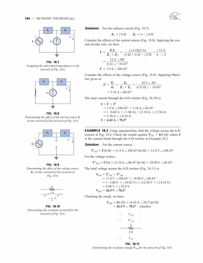
R
6 V
V′′6Ω+ –
V′6Ω+ –
V6Ω+ –
I
I′
R
6 VI′′
794 NETWORK THEOREMS (ac)
Solution: For the redrawn circuit (Fig. 18.7),
Z1 5 j 6 V Z2 5 6 2 j 8 V
Consider the effects of the current source (Fig. 18.8). Applying the cur-
rent divider rule, we have
I′ 5 5 5
5
I′ 5 1.9 A /108.43°
Consider the effects of the voltage source (Fig. 18.9). Applying Ohm’s
law gives us
I″ 5 5 5
5 3.16 A /48.43°
The total current through the 6-V resistor (Fig. 18.10) is
I 5 I′ 1 I″5 1.9 A /108.43° 1 3.16 A /48.43°
5 (20.60 A 1 j 1.80 A) 1 (2.10 A 1 j 2.36 A)
5 1.50 A 1 j 4.16 A
I 5 4.42 A /70.2°
EXAMPLE 18.3 Using superposition, find the voltage across the 6-V
resistor in Fig. 18.6. Check the results against V6V 5 I(6 V), where I
is the current found through the 6-V resistor in Example 18.2.
Solution: For the current source,
V′6V 5 I′(6 V) 5 (1.9 A /108.43°)(6 V) 5 11.4 V /108.43°
For the voltage source,
V″6V 5 I″(6) 5 (3.16 A /48.43°)(6 V) 5 18.96 V /48.43°
The total voltage across the 6-V resistor (Fig. 18.11) is
V6V 5 V′6V 1 V″6V
5 11.4 V /108.43° 1 18.96 V /48.43°
5 (23.60 V 1 j 10.82 V) 1 (12.58 V 1 j 14.18 V)
5 8.98 V 1 j 25.0 V
V6V 5 26.5 V /70.2°
Checking the result, we have
V6V 5 I(6 V) 5 (4.42 A /70.2°)(6 V)
5 26.5 V /70.2° (checks)
20 V /30°6.32 V /218.43°
E1Z1 1 Z2
E1ZT
12 A /90°6.32 /218.43°
j 12 A6 2 j 2
( j 6 V)(2 A)j 6 V 1 6 V 2 j 8 V
Z1I1Z1 1 Z2
Th
–
I
Z1 Z2
E1
+
I1
FIG. 18.7Assigning the subscripted impedances to the
network of Fig. 18.6.
I9
Z1 Z2
I1
FIG. 18.8Determining the effect of the current source I1
on the current I of the network of Fig. 18.6.
I0
Z1 Z2
–
E1
+
FIG. 18.9Determining the effect of the voltage source
E1 on the current I of the network of
Fig. 18.6.
FIG. 18.10Determining the resultant current I for the
network of Fig. 18.6.
FIG. 18.11Determining the resultant voltage V6V for the network of Fig. 18.6.

SUPERPOSITION THEOREM 795
Solution: For the dc source, recall that for dc analysis, in the steady
state the capacitor can be replaced by an open-circuit equivalent, and
the inductor by a short-circuit equivalent. The result is the network of
Fig. 18.13.
The resistors R1 and R3 are then in parallel, and the voltage V3 can
be determined using the voltage divider rule:
R′ 5 R1 \ R3 5 0.5 kV \ 3 kV 5 0.429 kV
and V3 5
5 5
V3 > 3.6 V
For ac analysis, the dc source is set to zero and the network is
redrawn, as shown in Fig. 18.14.
5.148 V
1.429
(0.429 kV)(12 V)0.429 kV 1 1 kV
R′E1R′ 1 R2
Th
–
+
R2 1 kV
R1
0.5 kV
XL
2 kV
R3 3 kV v3XC 10 kVE2 = 4 V ∠0°–
+
E1 = 12 V
FIG. 18.12Example 18.4.
EXAMPLE 18.4 For the network of Fig. 18.12, determine the sinu-
soidal expression for the voltage v3 using superposition.
–
+
R2 1 kV
R1
0.5 kV
R3 3 kV V3
E1 = 12 V
FIG. 18.13Determining the effect of the dc voltage source
E1 on the voltage v3 of the network of
Fig. 18.12.
XC = 10 kV
–
+R2 = 1 kV
R1
0.5 kV
R3 = 3 kV V3
XL
2 kV
E2 = 4 V ∠0°–
+
The block impedances are then defined as in Fig. 18.15, and series-
parallel techniques are applied as follows:
Z1 5 0.5 kV /0°
Z2 5 (R2 /0° \ (XC /290°)
5 5
5 0.995 kV /25.71°
10 kV /290°10.05 /284.29°
(1 kV /0°)(10 kV /290°)
1 kV 2 j 10 kV
FIG. 18.14Redrawing the network of Fig. 18.12 to determine the effect of the ac voltage
source E2.
–
Is
Z1
Z2E2
+
Z3
ZT
V3
–
+
I3
FIG. 18.15Assigning the subscripted impedances to the
network of Fig. 18.14.

(0.5,0)1((0.995/25.71)*(3.61/33.69))/((0.995/25.71)1(3.61/33.69)) Enter(1.311E0,35.373E23)
Ans c Pol(1.312E0/1.545E0)
796 NETWORK THEOREMS (ac)
Z3 5 R3 1 j XL 5 3 kV 1 j 2 kV 5 3.61 kV /33.69°
and
ZT 5 Z1 1 Z2 \ Z3
5 0.5 kV 1 (0.995 kV /25.71°) \ (3.61 kV /33.69°)
5 1.312 kV /1.57°
Calculator Performing the above on the TI-86 calculator gives the
following result:
Th
CALC. 18.1
Is 5 5 5 3.05 mA /21.57°
Current divider rule:
I3 5 5
5 0.686 mA /232.74°
with
V3 5 (I3 /v)(R3 /0°)
5 (0.686 mA /232.74°)(3 kV /0°)
5 2.06 V /232.74°
The total solution:
v3 5 v3 (dc) 1 v3 (ac)
5 3.6 V 1 2.06 V /232.74°
v3 5 3.6 1 2.91 sin(qt 2 32.74°)
The result is a sinusoidal voltage having a peak value of 2.91 V rid-
ing on an average value of 3.6 V, as shown in Fig. 18.16.
(0.995 kV /25.71°)(3.05 mA /21.57°)0.995 kV /25.71° 1 3.61 kV /33.69°
Z2IsZ2 1 Z3
4 V /0°1.312 kV /1.57°
E2ZT
6.51 V
3.6 V
0.69 V
0
v332.74°
qt
FIG. 18.16The resultant voltage v3 for the network of Fig. 18.12.
Dependent SourcesFor dependent sources in which the controlling variable is not deter-
mined by the network to which the superposition theorem is to be
applied, the application of the theorem is basically the same as for inde-

SUPERPOSITION THEOREM 797
pendent sources. The solution obtained will simply be in terms of the
controlling variables.
EXAMPLE 18.5 Using the superposition theorem, determine the cur-
rent I2 for the network of Fig. 18.17. The quantities m and h are con-
stants.
Th
–
+R2 6 V
XL 8 V
hI
R1
4 VI2I
–+ V
Vm
FIG. 18.17Example 18.5.
Solution: With a portion of the system redrawn (Fig. 18.18),
Z1 5 R1 5 4 V Z2 5 R2 1 j XL 5 6 1 j 8 V
For the voltage source (Fig. 18.19),
I′ 5 5 5
5 5 0.078 mV/V /238.66°
For the current source (Fig. 18.20),
I″ 5 5 5 4(0.078)hI /238.66°
5 0.312hI /238.66°
The current I2 is
I2 5 I′ 1 I″5 0.078 mV/V /238.66° 1 0.312hI /238.66°
For V 5 10 V /0°, I 5 20 mA /0°, m 5 20, and h 5 100,
I2 5 0.078(20)(10 V /0°)/V /238.66°
1 0.312(100)(20 mA/0°)/238.66°
5 15.60 A /238.66° 1 0.62 A /238.66°
I2 5 16.22 A /238.66°
For dependent sources in which the controlling variable is deter-
mined by the network to which the theorem is to be applied, the depen-
dent source cannot be set to zero unless the controlling variable is also
zero. For networks containing dependent sources such as indicated in
Example 18.5 and dependent sources of the type just introduced above,
the superposition theorem is applied for each independent source and
each dependent source not having a controlling variable in the portions
of the network under investigation. It must be reemphasized that depen-
(4 V)(hI)12.8 V /38.66°
Z1(hI)Z1 1 Z2
mV12.8 V /38.66°
mV10 V 1 j 8 V
mV4 V 1 6 V 1 j 8 V
mVZ1 1 Z2
–
Z1
+
Z2
I2
hI Vm
FIG. 18.18Assigning the subscripted impedances to the
network of Fig. 18.17.
–
Z1
V
+
Z2
I9
m
FIG. 18.19Determining the effect of the
voltage-controlled voltage source on the
current I2 for the network of Fig. 18.17.
Z1
Z2
I0
hI1
FIG. 18.20Determining the effect of the
current-controlled current source on the
current I2 for the network of Fig. 18.17.

798 NETWORK THEOREMS (ac)
dent sources are not sources of energy in the sense that, if all indepen-
dent sources are removed from a system, all currents and voltages must
be zero.
EXAMPLE 18.6 Determine the current IL through the resistor RL of
Fig. 18.21.
Solution: Note that the controlling variable V is determined by the
network to be analyzed. From the above discussions, it is understood
that the dependent source cannot be set to zero unless V is zero. If we
set I to zero, the network lacks a source of voltage, and V 5 0 with
mV 5 0. The resulting IL under this condition is zero. Obviously, there-
fore, the network must be analyzed as it appears in Fig. 18.21, with the
result that neither source can be eliminated, as is normally done using
the superposition theorem.
Applying Kirchhoff’s voltage law, we have
VL 5 V 1 mV 5 (1 1 m)V
and IL 5 5
The result, however, must be found in terms of I since V and mV are
only dependent variables.
Applying Kirchhoff’s current law gives us
I 5 I1 1 IL 5 1
and I 5 V1 1 2or V 5
Substituting into the above yields
IL 5 5 1 2Therefore, IL 5
18.3 THEVENIN’S THEOREMThévenin’s theorem, as stated for sinusoidal ac circuits, is changed
only to include the term impedance instead of resistance; that is,
any two-terminal linear ac network can be replaced with an
equivalent circuit consisting of a voltage source and an impedance in
series, as shown in Fig. 18.22.
Since the reactances of a circuit are frequency dependent, the Thévenin
circuit found for a particular network is applicable only at one fre-
quency.
The steps required to apply this method to dc circuits are repeated
here with changes for sinusoidal ac circuits. As before, the only change
(1 1 m)R1IRL 1 (1 1 m)R1
I(1/R1) 1 [(1 1 m)/RL]
(1 1 m)
RL
(1 1 m)V
RL
I(1/R1) 1 [(1 1 m)/RL]
1 1 m
RL
1R1
(1 1 m)V
RL
VR1
(1 1 m)V
RL
VLRL
Th
RL
mV– +
ILI1
R1 VI–
+
FIG. 18.21Example 18.6.
–
+
ZTh
ETh
FIG. 18.22Thévenin equivalent circuit for ac networks.

THÉVENIN’S THEOREM 799
is the replacement of the term resistance with impedance. Again,
dependent and independent sources will be treated separately.
Example 18.9, the last example of the independent source section,
will include a network with dc and ac sources to establish the ground-
work for possible use in the electronics area.
Independent Sources1. Remove that portion of the network across which the Thévenin
equivalent circuit is to be found.
2. Mark (C, , and so on) the terminals of the remaining two-terminal
network.
3. Calculate ZTh by first setting all voltage and current sources to
zero (short circuit and open circuit, respectively) and then finding
the resulting impedance between the two marked terminals.
4. Calculate ETh by first replacing the voltage and current sources
and then finding the open-circuit voltage between the marked
terminals.
5. Draw the Thévenin equivalent circuit with the portion of the
circuit previously removed replaced between the terminals of the
Thévenin equivalent circuit.
EXAMPLE 18.7 Find the Thévenin equivalent circuit for the network
external to resistor R in Fig. 18.23.
Th
R2 V
–
+
E = 10 V ∠ 0°
XL = 8 V
XC
Thévenin
FIG. 18.23Example 18.7.
Solution:Steps 1 and 2 (Fig. 18.24):
E = 10 V ∠ 0°–
+
Z1
Z2
Thévenin
FIG. 18.24Assigning the subscripted impedances to the network of Fig. 18.23.
Z1 5 j XL 5 j 8 V Z2 5 2j XC 5 2j 2 V
Step 3 (Fig. 18.25):
Z1
Z2
ZTh
FIG. 18.25Determining the Thévenin impedance for the
network of Fig. 18.23.

800 NETWORK THEOREMS (ac)
ZTh 5 5 5 5
5 2.67 V /290°
Step 4 (Fig. 18.26):
ETh 5 (voltage divider rule)
5 5 5 3.33 V /2180°
Step 5: The Thévenin equivalent circuit is shown in Fig. 18.27.
2j 20 V
j 6
(2j 2 V)(10 V)j 8 V 2 j 2 V
Z2EZ1 1 Z2
16 V6 /90°
2j 216 V
j 6
( j 8 V)(2j 2 V)
j 8 V 2 j 2 V
Z1Z2Z1 1 Z2
Th
Z1
Z2 ETh
–
+
E
+
–
FIG. 18.26Determining the open-circuit Thévenin
voltage for the network of Fig. 18.23.
–
+
ETh = 3.33 V ∠ – 180°
ZTh
R
ZTh = 2.67 V ∠ –90°
–
+
ETh = 3.33 V ∠ – 180° R
XC = 2.67 V
FIG. 18.27The Thévenin equivalent circuit for the network of Fig. 18.23.
EXAMPLE 18.8 Find the Thévenin equivalent circuit for the network
external to branch a-a′ in Fig. 18.28.
–
+
R3
7 V
R1
6 V
E1
XL1
8 V
R2 3 V
XL2= 5 V
10 V ∠ 0°XC 4 V
a
–
+
E2 30 V ∠ 15°
a9 Thévenin
FIG. 18.28Example 18.8.
Solution:Steps 1 and 2 (Fig. 18.29): Note the reduced complexity with sub-
scripted impedances:
E1
–
+
Z1
Z2
Z3
10 V ∠ 0°
a
a9 Thévenin
FIG. 18.29Assigning the subscripted impedances to the network of Fig. 18.28.
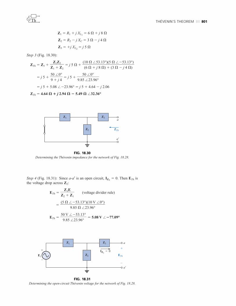
THÉVENIN’S THEOREM 801
Z1 5 R1 1 j XL15 6 V 1 j 8 V
Z2 5 R2 2 j XC 5 3 V 2 j 4 V
Z3 5 1j XL25 j 5 V
Step 3 (Fig. 18.30):
ZTh 5 Z3 1 5 j 5 V 1
5 j 5 1 5 j 5 1
5 j 5 1 5.08 /223.96° 5 j 5 1 4.64 2 j 2.06
ZTh 5 4.64 V 1 j 2.94 V 5 5.49 V /32.36°
50 /0°9.85 /23.96°
50 /0°9 1 j 4
(10 V /53.13°)(5 V /253.13°)(6 V 1 j 8 V) 1 (3 V 2 j 4 V)
Z1Z2Z1 1 Z2
Th
Z1
Z2
Z3a
a9
ZTh
FIG. 18.30Determining the Thévenin impedance for the network of Fig. 18.28.
Step 4 (Fig. 18.31): Since a-a′ is an open circuit, IZ35 0. Then ETh is
the voltage drop across Z2:
ETh 5 (voltage divider rule)
5
ETh 5 5 5.08 V /277.09°50 V /253.13°
9.85 /23.96°
(5 V /253.13°)(10 V /0°)
9.85 V /23.96°
Z2EZ2 1 Z1
E1
–
+
Z1
Z2
Z3 a
a9
ETh
–
+IZ3
= 0
FIG. 18.31Determining the open-circuit Thévenin voltage for the network of Fig. 18.28.

802 NETWORK THEOREMS (ac)
The next example demonstrates how superposition is applied to elec-
tronic circuits to permit a separation of the dc and ac analyses. The fact
that the controlling variable in this analysis is not in the portion of the net-
work connected directly to the terminals of interest permits an analysis of
the network in the same manner as applied above for independent sources.
EXAMPLE 18.9 Determine the Thévenin equivalent circuit for the
transistor network external to the resistor RL in the network of Fig.
18.33. Then determine VL.
Th
–
+
ETh
ZTh
R3
4.64 V + j2.94 V7 V
5.08 V ∠ –77.09°–
+
E2 30 V ∠ 15°–
+
ETh
4.64 V 7 V
5.08 V ∠ –77.09°
–
+
E2 30 V ∠ 15°
2.94 V
R XLa
a′
a
a′
R3
FIG. 18.32The Thévenin equivalent circuit for the network of Fig. 18.28.
–
+
RB 1 MV
RC 2 kV
Rs
0.5 kV
Ei
C1
10 V
12 V
C2
10 V
Transistor
RL = 1 kV VL
–
+
Thévenin
FIG. 18.33Example 18.9.
Solution: Applying superposition.
dc Conditions Substituting the open-circuit equivalent for the cou-
pling capacitor C2 will isolate the dc source and the resulting currents
from the load resistor. The result is that for dc conditions, VL 5 0 V.
Although the output dc voltage is zero, the application of the dc voltage
is important to the basic operation of the transistor in a number of
important ways, one of which is to determine the parameters of the
“equivalent circuit” to appear in the ac analysis to follow.
ac Conditions For the ac analysis, an equivalent circuit is substi-
tuted for the transistor, as established by the dc conditions above, that
Step 5: The Thévenin equivalent circuit is shown in Fig. 18.32.

THÉVENIN’S THEOREM 803
will behave like the actual transistor. A great deal more will be said
about equivalent circuits and the operations performed to obtain the net-
work of Fig. 18.34, but for now let us limit our attention to the manner
in which the Thévenin equivalent circuit is obtained. Note in Fig. 18.34
that the equivalent circuit includes a resistor of 2.3 kV and a controlled
current source whose magnitude is determined by the product of a fac-
tor of 100 and the current I1 in another part of the network.
Th
RB 1 MV
Rs
0.5 kV
–
+
I1
2.3 kV RC 2 kV RL 1 kV VLEi100I1
Transistor equivalentcircuit
–
+
Thévenin
FIG. 18.34The ac equivalent network for the transistor amplifier of Fig. 18.33.
Note in Fig. 18.34 the absence of the coupling capacitors for the ac
analysis. In general, coupling capacitors are designed to be open cir-
cuits for dc analysis and short circuits for ac analysis. The short-circuit
equivalent is valid because the other impedances in series with the cou-
pling capacitors are so much larger in magnitude that the effect of the
coupling capacitors can be ignored. Both RB and RC are now tied to
ground because the dc source was set to zero volts (superposition) and
replaced by a short-circuit equivalent to ground.
For the analysis to follow, the effect of the resistor RB will be
ignored since it is so much larger than the parallel 2.3-kV resistor.
ZTh When Ei is set to zero volts, the current I1 will be zero amperes,
and the controlled source 100I1 will be zero amperes also. The result is
an open-circuit equivalent for the source, as appearing in Fig. 18.35.
It is fairly obvious from Fig. 18.35 that
ZTh 5 2 kV
ETh For ETh, the current I1 of Fig. 18.34 will be
I1 5 5 5
and 100I1 5 (100)1 2 5 35.71 3 1023/V Ei
Referring to Fig. 18.36, we find that
ETh 5 2(100I1)RC
5 2(35.71 3 1023/V Ei)(2 3 103V)
ETh 5 271.42Ei
The Thévenin equivalent circuit appears in Fig. 18.37 with the orig-
inal load RL.
Ei2.8 kV
Ei2.8 kV
Ei0.5 kV 1 2.3 kV
EiRs 1 2.3 kV
RC 2 kV ZTh
FIG. 18.35Determining the Thévenin impedance for the
network of Fig. 18.34.
–
+
RC 2 kV ETh
–
+
100I1
FIG. 18.36Determining the Thévenin voltage for the net-
work of Fig. 18.34.
–
+
ETh RL
RTh
2 kV
1 kV VL
–
+
71.42Ei
FIG. 18.37The Thévenin equivalent circuit for the net-
work of Fig. 18.34.

Th804 NETWORK THEOREMS (ac)
Output Voltage VL
VL 5 5
and VL 5 223.81Ei
revealing that the output voltage is 23.81 times the applied voltage with
a phase shift of 180° due to the minus sign.
Dependent SourcesFor dependent sources with a controlling variable not in the network
under investigation, the procedure indicated above can be applied. How-
ever, for dependent sources of the other type, where the controlling vari-
able is part of the network to which the theorem is to be applied, another
approach must be employed. The necessity for a different approach will be
demonstrated in an example to follow. The method is not limited to depen-
dent sources of the latter type. It can also be applied to any dc or sinusoidal
ac network. However, for networks of independent sources, the method of
application employed in Chapter 9 and presented in the first portion of this
section is generally more direct, with the usual savings in time and errors.
The new approach to Thévenin’s theorem can best be introduced at
this stage in the development by considering the Thévenin equivalent
circuit of Fig. 18.38(a). As indicated in Fig. 18.38(b), the open-circuit
terminal voltage (Eoc) of the Thévenin equivalent circuit is the Thévenin
equivalent voltage; that is,
(18.1)
If the external terminals are short circuited as in Fig. 18.38(c), the
resulting short-circuit current is determined by
(18.2)
or, rearranged,
ZTh 5
and (18.3)
Equations (18.1) and (18.3) indicate that for any linear bilateral dc or
ac network with or without dependent sources of any type, if the open-
circuit terminal voltage of a portion of a network can be determined
along with the short-circuit current between the same two terminals, the
Thévenin equivalent circuit is effectively known. A few examples will
make the method quite clear. The advantage of the method, which was
stressed earlier in this section for independent sources, should now be
more obvious. The current Isc, which is necessary to find ZTh, is in gen-
eral more difficult to obtain since all of the sources are present.
There is a third approach to the Thévenin equivalent circuit that is
also useful from a practical viewpoint. The Thévenin voltage is found
as in the two previous methods. However, the Thévenin impedance is
ZTh 5 E
Is
o
c
c
EThIsc
Isc 5 E
ZT
T
h
h
Eoc 5 ETh
2(1 kV)(71.42Ei)
1 kV 1 2 kV
2RLEThRL 1 ZTh
–
+
ZTh
ETh
–
+
ZTh
ETh
–
+
ZTh
ETh
Eoc = ETh
–
+
Isc =ETh
ZTh
(a)
(b)
(c)
FIG. 18.38Defining an alternative approach for
determining the Thévenin impedance.

THÉVENIN’S THEOREM 805
obtained by applying a source of voltage to the terminals of interest and
determining the source current as indicated in Fig. 18.39. For this
method, the source voltage of the original network is set to zero. The
Thévenin impedance is then determined by the following equation:
(18.4)
Note that for each technique, ETh 5 Eoc, but the Thévenin impedance is
found in different ways.
EXAMPLE 18.10 Using each of the three techniques described in this
section, determine the Thévenin equivalent circuit for the network of
Fig. 18.40.
Solution: Since for each approach the Thévenin voltage is found in
exactly the same manner, it will be determined first. From Fig. 18.40,
where IXC 5 0,
Due to the polarity for V and
defined terminal polarities
VR15 ETh 5 Eoc 5 2 5 2
The following three methods for determining the Thévenin imped-
ance appear in the order in which they were introduced in this section.
Method 1: See Fig. 18.41.
ZTh 5 R1 \ R2 2 j XC
Method 2: See Fig. 18.42. Converting the voltage source to a current
source (Fig. 18.43), we have (current divider rule)
Isc 5 5
5
R
2
1
m
1
R2
R
V
2
——(R1 i R2) 2 j XC
2R1
R
1
1R2
R2
1m
R
V
1
2——(R1 i R2) 2 j XC
2(R1 i R2)m
R
V
1
——(R1 i R2) 2 j XC
mR2VR1 1 R2
R2(mV)R1 1 R2
ZTh 5 E
Ig
g
Th
Ig
–
+
ZTh
Network Eg
FIG. 18.39Determining ZTh using the approach
ZTh 5 Eg / Ig.
–
+
R1
R2
Thévenin
XC
mV
–
+
m
FIG. 18.40Example 18.10.
R1
R2 ZTh
XC
–
+R2
R1
mV
XC
Isc
Isc
m
R1 R2 Isc
XC
mV
R1
Isc
m
FIG. 18.41Determining the Thévenin impedance for the
network of Fig. 18.40.
FIG. 18.42Determining the short-circuit current for the
network of Fig. 18.40.
FIG. 18.43Converting the voltage source of Fig. 18.42 to a current source.

Th806 NETWORK THEOREMS (ac)
and
ZTh 5 5 5
(R1 i R2) 2 j XC
5 R1 i R2 2 j XC
Method 3: See Fig. 18.44.
Ig 5
and ZTh 5 5 R1 \ R2 2 j XC
In each case, the Thévenin impedance is the same. The resulting
Thévenin equivalent circuit is shown in Fig. 18.45.
EgIg
Eg(R1 \ R2) 2 j XC
1––––
(R1 i R2
1
) 2 j XC
R
2
1
m
1
R2
R
V
2
––––
R
2
1
m
1
R2
R
V
2
EocIsc
R2
R1XC Ig
+
–
Eg
ZTh
FIG. 18.44Determining the Thévenin impedance for the
network of Fig. 18.40 using the approach
ZTh 5 Eg / Ig.
R1 + R2
ETh = Thévenin
–
+
mR2V
ZTh = R1 \ R2 – jXC
–
+
m
FIG. 18.45The Thévenin equivalent circuit for the network of Fig. 18.40.
EXAMPLE 18.11 Repeat Example 18.10 for the network of Fig.
18.46.
Solution: From Fig. 18.46, ETh is
ETh 5 Eoc 5 2hI(R1 \ R2) 5 2
Method 1: See Fig. 18.47.
ZTh 5 R1 \ R2 2 j XC
Note the similarity between this solution and that obtained for the pre-
vious example.
Method 2: See Fig. 18.48.
Isc 5
and ZTh 5 5 5 R1 i R2 2 j XC
2hI(R1 i R2)——
(R
2
1
(
i
R
R
1
2
i
)
R
2
2)
j
h
X
I
C
EocIsc
2(R1 \ R2)hI(R1 \ R2) 2 j XC
hR1R2IR1 1 R2
hI R1 R2
XC
Thévenin
FIG. 18.46Example 18.11.
R1 R2
XC
ZTh = R1 i R2 – jXC
FIG. 18.47Determining the Thévenin impedance for the
network of Fig. 18.46.

THÉVENIN’S THEOREM 807
Method 3: See Fig. 18.49.
Ig 5
and ZTh 5 5 R1 \ R2 2 j XC
The following example has a dependent source that will not permit
the use of the method described at the beginning of this section for
independent sources. All three methods will be applied, however, so
that the results can be compared.
EXAMPLE 18.12 For the network of Fig. 18.50 (introduced in Exam-
ple 18.6), determine the Thévenin equivalent circuit between the indi-
cated terminals using each method described in this section. Compare
your results.
EgIg
Eg(R1 \ R2) 2 j XC
Th
Solution: First, using Kirchhoff’s voltage law, ETh (which is the
same for each method) is written
ETh 5 V 1 mV 5 (1 1 m)V
However, V 5 IR1
so ETh 5 (1 1 m)IR1
ZThMethod 1: See Fig. 18.51. Since I 5 0, V and mV 5 0, and
ZTh 5 R1 (incorrect)
Method 2: See Fig. 18.52. Kirchhoff’s voltage law around the indicated
loop gives us
V 1 mV 5 0
and V(1 1 m) 5 0
Since m is a positive constant, the above equation can be satisfied
only when V 5 0. Substitution of this result into Fig. 18.52 will yield
the configuration of Fig. 18.53, and
Isc 5 I
hI R1 R2
XC
Isc
Isc
FIG. 18.48Determining the short-circuit current for the
network of Fig. 18.46.
R1 R2
XC
Eg
Ig
–
+
ZTh
FIG. 18.49Determining the Thévenin impedance using
the approach ZTh 5 Eg / Ig.
I R1
mV
Thévenin
V
+
–
+–m
FIG. 18.50Example 18.12.
R1
mV = 0
V = 0
+
–
+–
ZTh
m
FIG. 18.51Determining ZTh incorrectly.
FIG. 18.52Determining Isc for the network of Fig. 18.50.
I R1
mV
V
+
–
+–
Isc
Isc
m

808 NETWORK THEOREMS (ac)
with
ZTh 5 5 5 (1 1 m)R1 (correct)
Method 3: See Fig. 18.54.
Eg 5 V 1 mV 5 (1 1 m)V
or V 5
and Ig 5 5
and ZTh 5 5 (1 1 m)R1 (correct)
The Thévenin equivalent circuit appears in Fig. 18.55, and
IL 5
which compares with the result of Example 18.6.
The network of Fig. 18.56 is the basic configuration of the transistor
equivalent circuit applied most frequently today (although most texts in
electronics will use the circle rather than the diamond outline for the
source). Obviously, it is necessary to know its characteristics and to be
adept in its use. Note that there are both a controlled voltage and a con-
trolled current source, each controlled by variables in the configuration.
(1 1 m)R1IRL 1 (1 1 m)R1
EgIg
Eg
(1 1 m)R1
VR1
Eg
1 1 m
(1 1 m)IR1
I
EocIsc
Th
–
+
R1 V Eg
IgmV
+–
ZTh
m
FIG. 18.54Determining ZTh using the approach ZTh 5
Eg / Ig.
–
+
(1 + m)R1
RL
IL
ETh = (1 + m)IR1
FIG. 18.55The Thévenin equivalent circuit for the
network of Fig. 18.50.
–
+
R2k2Ik1V2Vi
I
R1
Thévenin
–
+
V2
–
+
FIG. 18.56Example 18.13: Transistor equivalent network.
EXAMPLE 18.13 Determine the Thévenin equivalent circuit for the
indicated terminals of the network of Fig. 18.56.
Solution: Apply the second method introduced in this section.
EThEoc 5 V2
I 5 5
and Eoc 5 2k2IR2 5 2k2R21 25 1
k1k2R2Eoc
R1
2k2R2Vi
R1
Vi 2 k1Eoc
R1
Vi 2 k1Eoc
R1
Vi 2 k1V2
R1
I R1 V = 0
+
–Isc
I1 = 0 Isc
FIG. 18.53Substituting V 5 0 into the network of Fig.
18.52.

THÉVENIN’S THEOREM 809
or Eoc11 2 2 5
and Eoc1 2 5
so (18.5)
Isc For the network of Fig. 18.57, where
V2 5 0 k1V2 5 0 I 5
and Isc 5 2k2I 5
so ZTh 5 5 5
and (18.6)ZTh 5
R2
1 2 k1k
R
2
1
R2
R1R2——R12k1k2R2
R
2
12
k2
k
R
1k
2V
2R
i
2
–––
2
R
k2
1
Vi
EocIsc
2k2Vi
R1
ViR1
Eoc 5 R1
2
2
k2
k
R
1
2
k
V
2R
i
2
5 ETh
2k2R2Vi
R1
R1 2 k1k2R2
R1
2k2R2Vi
R1
k1k2R2
R1
Th
Isc
–
+
R2k2IVi
I
R1
Isc
FIG. 18.57Determining Isc for the network of Fig. 18.56.
Frequently, the approximation k1 > 0 is applied. Then the Thévenin
voltage and impedance are
k1 5 0 (18.7)
k1 5 0 (18.8)
Apply ZTh 5 Eg/Ig to the network of Fig. 18.58, where
I 5
But V2 5 Eg
so I 52k1Eg
R1
2k1V2
R1
ZTh 5 R2
ETh 5 2k
R
2R
1
2Vi
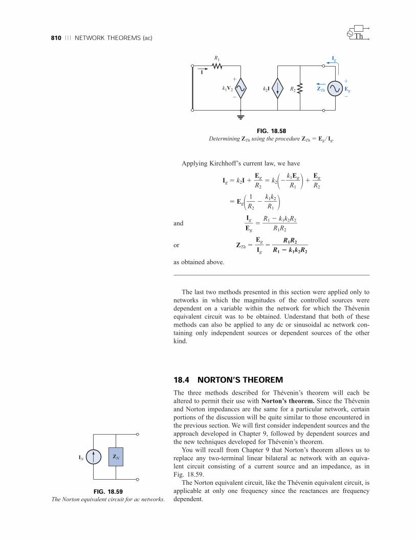
810 NETWORK THEOREMS (ac) Th
ZTh
–
+
Eg
Ig
R2k2Ik1V2
I
R1
–
+
FIG. 18.58Determining ZTh using the procedure ZTh 5 Eg / Ig.
Applying Kirchhoff’s current law, we have
Ig 5 k2I 1 5 k212 2 1
5 Eg1 2 2and 5
or ZTh 5 5
as obtained above.
The last two methods presented in this section were applied only to
networks in which the magnitudes of the controlled sources were
dependent on a variable within the network for which the Thévenin
equivalent circuit was to be obtained. Understand that both of these
methods can also be applied to any dc or sinusoidal ac network con-
taining only independent sources or dependent sources of the other
kind.
18.4 NORTON’S THEOREMThe three methods described for Thévenin’s theorem will each be
altered to permit their use with Norton’s theorem. Since the Thévenin
and Norton impedances are the same for a particular network, certain
portions of the discussion will be quite similar to those encountered in
the previous section. We will first consider independent sources and the
approach developed in Chapter 9, followed by dependent sources and
the new techniques developed for Thévenin’s theorem.
You will recall from Chapter 9 that Norton’s theorem allows us to
replace any two-terminal linear bilateral ac network with an equiva-
lent circuit consisting of a current source and an impedance, as in
Fig. 18.59.
The Norton equivalent circuit, like the Thévenin equivalent circuit, is
applicable at only one frequency since the reactances are frequency
dependent.
R1R2R1 2 k1k2R2
EgIg
R1 2 k1k2R2
R1R2
IgEg
k1k2R1
1R2
EgR2
k1Eg
R1
EgR2
ZNIN
FIG. 18.59The Norton equivalent circuit for ac networks.

NORTON’S THEOREM 811Th
Independent SourcesThe procedure outlined below to find the Norton equivalent of a sinu-
soidal ac network is changed (from that in Chapter 9) in only one
respect: the replacement of the term resistance with the term imped-
ance.
1. Remove that portion of the network across which the Norton
equivalent circuit is to be found.
2. Mark (C, , and so on) the terminals of the remaining two-terminal
network.
3. Calculate ZN by first setting all voltage and current sources to
zero (short circuit and open circuit, respectively) and then
finding the resulting impedance between the two marked
terminals.
4. Calculate IN by first replacing the voltage and current sources and
then finding the short-circuit current between the marked
terminals.
5. Draw the Norton equivalent circuit with the portion of the circuit
previously removed replaced between the terminals of the Norton
equivalent circuit.
The Norton and Thévenin equivalent circuits can be found from each
other by using the source transformation shown in Fig. 18.60. The
source transformation is applicable for any Thévenin or Norton equiva-
lent circuit determined from a network with any combination of inde-
pendent or dependent sources.
–
+
ZTh
ETh = INZNZNIN =
ETh
ZTh
ZN = ZTh
ZTh = ZN
FIG. 18.60Conversion between the Thévenin and Norton equivalent circuits.
EXAMPLE 18.14 Determine the Norton equivalent circuit for the net-
work external to the 6-V resistor of Fig. 18.61.
–
+
RL 6 V
R1
3 V
E = 20 V ∠ 0°
XL
4 V
XC 5 V
Norton
FIG. 18.61Example 18.14.

812 NETWORK THEOREMS (ac)
Solution:Steps 1 and 2 (Fig. 18.62):
Z1 5 R1 1 j XL 5 3 V 1 j 4 V 5 5 V /53.13°
Z2 5 2j XC 5 2j 5 V
Step 3 (Fig. 18.63):
ZN 5 5 5
5 5 7.91 V /218.44° 5 7.50 V 2 j 2.50 V
Step 4 (Fig. 18.64):
IN 5 I1 5 5 5 4 A /253.13°20 V /0°
5 V /53.13°
EZ1
25 V /236.87°3.16 /218.43°
25 V /236.87°
3 2 j 1
(5 V /53.13°)(5 V /290°)
3 V 1 j 4 V 2 j 5 V
Z1Z2Z1 1 Z2
Th
E
–
+
Z1
Z2
Norton
FIG. 18.62Assigning the subscripted impedances to the
network of Fig. 18.61.
Z1
Z2 ZN
FIG. 18.63Determining the Norton impedance for the
network of Fig. 18.61.
E
–
+
Z1
Z2
I1
IN
IN
FIG. 18.64Determining IN for the network of Fig. 18.61.
R 6 VZNIN = 4 A ∠ – 53.13° RL 6 VIN = 4 A ∠ – 53.13°
R 7.50 V
XC 2.50 V
7.50 V – j2.50 V
Step 5: The Norton equivalent circuit is shown in Fig. 18.65.
FIG. 18.65The Norton equivalent circuit for the network of Fig. 18.61.
EXAMPLE 18.15 Find the Norton equivalent circuit for the network
external to the 7-V capacitive reactance in Fig. 18.66.
R2
1 V
R1 2 V
XC14 V
I = 3 A ∠ 0°XC2
= 7 V
XL
5 V
FIG. 18.66Example 18.15.

NORTON’S THEOREM 813
Solution:Steps 1 and 2 (Fig. 18.67):
Z1 5 R1 2 j XC15 2 V 2 j 4 V
Z2 5 R2 5 1 V
Z3 5 1j XL 5 j 5 V
Th
I = 3 A ∠ 0° Z1
Z2
Z3
FIG. 18.67Assigning the subscripted impedances to the network of Fig. 18.66.
Step 3 (Fig. 18.68):
ZN 5
Z1 1 Z2 5 2 V 2 j 4 V 1 1 V 5 3 V 2 j 4 V 5 5 V /253.13°
ZN 5 5
5
ZN 5 7.91 V /18.44° 5 7.50 V 1 j 2.50 V
25 V /36.87°3.16 /118.43°
25 V /36.87°
3 1 j 1
(5 V /90°)(5 V /253.13°)
j 5 V 1 3 V 2 j 4 V
Z3(Z1 1 Z2)Z3 1 (Z1 1 Z2)
Z1
Z2
Z3
ZN
Z1
Z2
Z3 ZN
FIG. 18.68Finding the Norton impedance for the network of Fig. 18.66.
Calculator Performing the above on the TI-86 calculator, we obtain
the following:
((0,5)*((2,24)1(1,0)))/((0,5)1((2,24)1(1,0)))(7.500E0,2.500E0)
Ans c Pol(7.906E0/18.435E0)
CALC. 18.2

814 NETWORK THEOREMS (ac)
Step 4 (Fig. 18.69):
IN 5 I1 5 (current divider rule)
5 5 5
IN 5 2.68 A /210.3°
13.4 A /263.43°
5 /253.13°
6 A 2 j 12 A5 /253.13°
(2 V 2 j 4 V)(3 A)
3 V 2 j 4 V
Z1IZ1 1 Z2
Th
I = 3 A ∠ 0°Z1
Z2
Z3
I1
IN
FIG. 18.69Determining IN for the network of Fig. 18.66.
Step 5: The Norton equivalent circuit is shown in Fig. 18.70.
XC27 V
7.50 V + j2.50 V
ZNIN = 2.68 A ∠ – 10.3° IN = 2.68 A ∠ – 10.3°
R 7.50 V
XL 2.50 V
XC27 V
FIG. 18.70The Norton equivalent circuit for the network of Fig. 18.66.
EXAMPLE 18.16 Find the Thévenin equivalent circuit for the net-
work external to the 7-V capacitive reactance in Fig. 18.66.
Solution: Using the conversion between sources (Fig. 18.71), we
obtain
ZTh 5 ZN 5 7.50 V 1 j 2.50 V
ETh 5 INZN 5 (2.68 A /210.3°)(7.91 V /18.44°)
5 21.2 V /8.14°
The Thévenin equivalent circuit is shown in Fig. 18.72.
Dependent SourcesAs stated for Thévenin’s theorem, dependent sources in which the con-
trolling variable is not determined by the network for which the Norton
equivalent circuit is to be found do not alter the procedure outlined
above.
For dependent sources of the other kind, one of the following proce-
dures must be applied. Both of these procedures can also be applied to
networks with any combination of independent sources and dependent
sources not controlled by the network under investigation.
FIG. 18.71Determining the Thévenin equivalent circuit
for the Norton equivalent of Fig. 18.70.
ZTh = ZN
INZNETh
+
–
ZTh
FIG. 18.72The Thévenin equivalent circuit for the net-
work of Fig. 18.66.
21.2 V ∠ 8.14°
R
7.50 V
ETh
+
–
XL
2.50 V
XC27 V

NORTON’S THEOREM 815
The Norton equivalent circuit appears in Fig. 18.73(a). In Fig.
18.73(b), we find that
Th
IN
(a)
ZN IN
(b)
ZN
I = 0
Isc IN
(c)
ZN
+
–
Eoc = INZN
FIG. 18.73Defining an alternative approach for determining ZN.
(18.9)
and in Fig. 18.73(c) that
Eoc 5 INZN
Or, rearranging, we have
ZN 5
and (18.10)
The Norton impedance can also be determined by applying a source
of voltage Eg to the terminals of interest and finding the resulting Ig, as
shown in Fig. 18.74. All independent sources and dependent sources not
controlled by a variable in the network of interest are set to zero, and
(18.11)
For this latter approach, the Norton current is still determined by the
short-circuit current.
EXAMPLE 18.17 Using each method described for dependent sources,
find the Norton equivalent circuit for the network of Fig. 18.75.
Solution:IN For each method, IN is determined in the same manner. From Fig.
18.76, using Kirchhoff’s current law, we have
0 5 I 1 hI 1 Isc
or Isc 5 2(1 1 h)I
Applying Kirchhoff’s voltage law gives us
ZN 5 E
Ig
g
ZN 5 E
Is
o
c
c
EocIN
Isc 5 IN
+
NetworkZN
Ig
Eg
–
FIG. 18.74Determining the Norton impedance using the
approach ZN 5 Eg / Ig.
R2
+
hIE
–
Norton
R1
I
FIG. 18.75Example 18.17.
R2
+
hIE
–
Isc
R1
I + –VR2
Isc
FIG. 18.76Determining Isc for the network of Fig. 18.75.

816 NETWORK THEOREMS (ac)
E 1 IR1 2 IscR2 5 0
and IR1 5 IscR2 2 E
or I 5
so Isc 5 2(1 1 h)I 5 2(1 1 h)1 2or R1Isc 5 2(1 1 h)IscR2 1 (1 1 h)E
Isc[R1 1 (1 1 h)R2] 5 (1 1 h)E
Isc 5 5 IN
ZNMethod 1: Eoc is determined from the network of Fig. 18.77. By
Kirchhoff’s current law,
0 5 I 1 hI or I(h 1 1) 5 0
For h, a positive constant I must equal zero to satisfy the above.
Therefore,
I 5 0 and hI 5 0
and Eoc 5 E
with ZN 5 5 5
Method 2: Note Fig. 18.78. By Kirchhoff’s current law,
Ig 5 I 1 hI 5 (1 1 h)I
R1 1 (1 1 h)R2––––
(1 1 h)
E––––
R1 1
(1
(
1
1 1
h)E
h)R2
EocIsc
(1 1 h)ER1 1 (1 1 h)R2
Isc R2 2 E
R1
Isc R2 2 E
R1
Th
+
hIE
–Eoc
R1
I+V = 0
–
+
–
FIG. 18.77Determining Eoc for the network of Fig. 18.75.
+
hI Eg
–
R1
I+–
ZN
Ig
R2
+– VR1VR2
FIG. 18.78Determining the Norton impedance using the approach ZN 5 Eg / Eg.
By Kirchhoff’s voltage law,
Eg 2 IgR2 2 IR1 5 0
or I 5
Substituting, we have
Ig 5 (1 1 h)I 5 (1 1 h)1 2and IgR1 5 (1 1 h)Eg 2 (1 1 h)IgR2
Eg 2 IgR2
R1
Eg 2 IgR2
R1

MAXIMUM POWER TRANSFER THEOREM 817
so Eg(1 1 h) 5 Ig[R1 1 (1 1 h)R2]
or ZN 5 5
which agrees with the above.
EXAMPLE 18.18 Find the Norton equivalent circuit for the network
configuration of Fig. 18.56.
Solution: By source conversion,
IN 5 5
and (18.12)
which is Isc as determined in Example 18.13, and
ZN 5 ZTh 5 (18.13)
For k1 > 0, we have
k1 5 0 (18.14)
k1 5 0 (18.15)
18.5 MAXIMUM POWER TRANSFER THEOREMWhen applied to ac circuits, the maximum power transfer theorem
states that
maximum power will be delivered to a load when the load impedance
is the conjugate of the Thévenin impedance across its terminals.
That is, for Fig. 18.79, for maximum power transfer to the load,
(18.16)
or, in rectangular form,
(18.17)
The conditions just mentioned will make the total impedance of the cir-
cuit appear purely resistive, as indicated in Fig. 18.80:
RL 5 RTh and 6j Xload 5 7j XTh
ZL 5 ZTh and vL 5 2vThZ
ZN 5 R2
IN 5 2
R
k2
1
Vi
R2——
1 2 k1k
R2
1
R2
IN 5 2
R
k2
1
Vi
—R1
2
2
k2
k
R
1
2
k
V
2R
i
2
—
——
—R1 2
R1
k
R
1
2
k2R2
—
EThZTh
R1 1 (1 1 h)R2
1 1 h
EgIg
Th
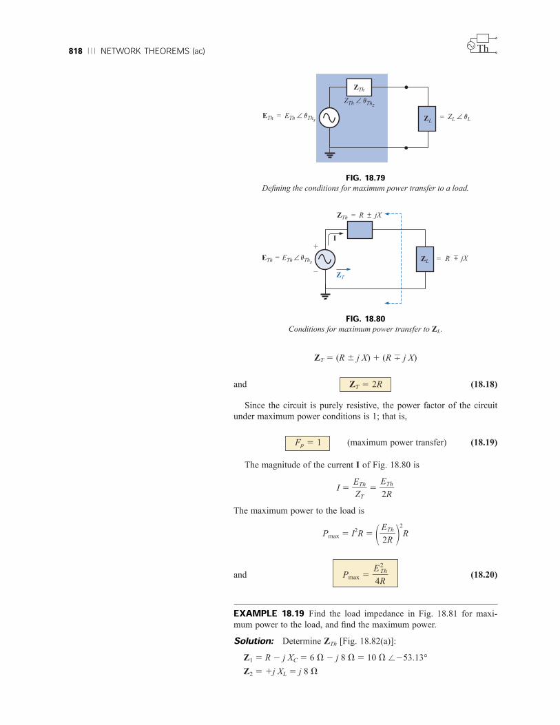
818 NETWORK THEOREMS (ac)
ZT 5 (R 6 j X) 1 (R 7 j X)
and (18.18)
Since the circuit is purely resistive, the power factor of the circuit
under maximum power conditions is 1; that is,
(maximum power transfer) (18.19)
The magnitude of the current I of Fig. 18.80 is
I 5 5
The maximum power to the load is
Pmax 5 I2R 5 1 22
R
and (18.20)
EXAMPLE 18.19 Find the load impedance in Fig. 18.81 for maxi-
mum power to the load, and find the maximum power.
Solution: Determine ZTh [Fig. 18.82(a)]:
Z1 5 R 2 j XC 5 6 V 2 j 8 V 5 10 V /253.13°
Z2 5 1j XL 5 j 8 V
Pmax 5 E
4R
2Th
ETh2R
ETh2R
EThZT
Fp 5 1
ZT 5 2R
Th
ETh = ETh ∠ vThs
ZTh
ZL
ZTh ∠ vThz
= ZL ∠ vL
FIG. 18.79Defining the conditions for maximum power transfer to a load.
ZTh = R ± jX
ZLETh = ETh ∠ vThs
+
– ZT
= R
±
jX
I
FIG. 18.80Conditions for maximum power transfer to ZL.

MAXIMUM POWER TRANSFER THEOREM 819
ZTh 5 5 5
5 13.33 V /36.87° 5 10.66 V 1 j 8 V
and ZL 5 13.3 V /236.87° 5 10.66 V 2 j 8 V
To find the maximum power, we must first find ETh [Fig. 18.82(b)],
as follows:
ETh 5 (voltage divider rule)
5 5 5 12 V /90°
Then Pmax 5 5 5 5 3.38 W
EXAMPLE 18.20 Find the load impedance in Fig. 18.83 for
maximum power to the load, and find the maximum power.
Solution: First we must find ZTh (Fig. 18.84).
Z1 5 1j XL 5 j 9 V Z2 5 R 5 8 V
Converting from a D to a Y (Fig. 18.85), we have
Z′1 5 5 j 3 V Z2 5 8 VZ13
14442.64
(12 V)24(10.66 V)
E2Th
4R
72 V /90°6 /0°
(8 V /90°)(9 V /0°)j 8 V 1 6 V 2 j 8 V
Z2EZ2 1 Z1
80 V /36.87°
6 /0°
(10 V /253.13°)(8 V /90°)
6 V 2 j 8 V 1 j 8 V
Z1Z2Z1 1 Z2
Th
E = 9 V ∠ 0°
R
6 V+
–
XC
8 V
XL 8 V ZL
FIG. 18.81Example 18.19.
(a)
Z2
Z1
ZTh
(b)
E
+
Z2
+
–
ETh
Z1
–
FIG. 18.82Determining (a) ZTh and (b) ETh for the network external to the load in
Fig. 18.81.
R
8 VZL
E =10 V∠ 0°
+
–
XL
9 V
XL
9 V9 V
XL
FIG. 18.83Example 18.20.

Th820 NETWORK THEOREMS (ac)
The redrawn circuit (Fig. 18.86) shows
ZTh 5 Z′1 1
5 j 3 V 1
5 j 3 1
5 j 3 1 5 j 3 1 2.56 /73.69°
5 j 3 1 0.72 1 j 2.46
ZTh 5 0.72 V 1 j 5.46 V
and ZL 5 0.72 V 2 j 5.46 V
For ETh, use the modified circuit of Fig. 18.87 with the voltage
source replaced in its original position. Since I1 5 0, ETh is the voltage
across the series impedance of Z′1 and Z2. Using the voltage divider
rule gives us
ETh 5 5
5
ETh 5 8.54 V /216.31°
(8.54 /20.56°)(10 V /0°)
10 /36.87°
( j 3 V 1 8 V)(10 V /0°)
8 V 1 j 6 V
(Z′1 1 Z2)EZ′1 1 Z2 1 Z′1
25.62 /110.56°10 /36.87°
(3 /90°)(8.54 /20.56°)
10 /36.87°
3 V /90°( j 3 V 1 8 V)
j 6 V 1 8 V
Z′1(Z′1 1 Z2)Z′1 1 (Z′1 1 Z2 )
ZTh
Z1
Z2
Z1
Z11
2
3
FIG. 18.84Defining the subscripted impedances for the network of Fig. 18.83.
ZTh
Z2
1
2
3
Z91
Z91 Z91
FIG. 18.85Substituting the Y equivalent for the upper D configuration of Fig. 18.84.
ZTh
Z91Z91
Z2
Z91
FIG. 18.86Determining ZTh for the network of Fig. 18.83.
ETh
Z91Z91
Z2
Z91+
–
I1 = 0
E
+
–
FIG. 18.87Finding the Thévenin voltage for the network
of Fig. 18.83.

MAXIMUM POWER TRANSFER THEOREM 821
and Pmax 5 5 5 W
5 25.32 W
If the load resistance is adjustable but the magnitude of the load
reactance cannot be set equal to the magnitude of the Thévenin reac-
tance, then the maximum power that can be delivered to the load
will occur when the load reactance is made as close to the Thévenin
reactance as possible and the load resistance is set to the following
value:
(18.21)
where each reactance carries a positive sign if inductive and a negative
sign if capacitive.
The power delivered will be determined by
(18.22)
where (18.23)
The derivation of the above equations is given in Appendix G of the
text. The following example demonstrates the use of the above.
EXAMPLE 18.21 For the network of Fig. 18.88:
Rav 5 RTh
2
1 RL
P 5 E2Th/4Rav
RL 5 ÏRw2Thw 1w (wXwThw 1w Xwlowadw)2w
72.932.88
(8.54 V)2
4(0.72 V)
E2Th
4R
Th
+
–
RTh
ETh = 20 V ∠0°
XTh
RL
4 V 7 V
XC = 4 V
FIG. 18.88Example 18.21.
a. Determine the value of RL for maximum power to the load if the
load reactance is fixed at 4 V.
b. Find the power delivered to the load under the conditions of part (a).
c. Find the maximum power to the load if the load reactance is made
adjustable to any value, and compare the result to part (b) above.
Solutions:a. Eq. (18.21): RL 5 ÏRw2
Thw 1w (wXwThw 1w Xwlowadw)2w5 Ï(4w Vw)2w 1w (w7w Vw 2w 4w Vw)2w

Th822 NETWORK THEOREMS (ac)
5 Ï1w6w 1w 9w 5 Ï2w5wRL 5 5 V
b. Eq. (18.23): Rav 5 5
5 4.5 V
Eq. (18.22): P 5
5 5 W
> 22.22 W
c. For ZL 5 4 V 2 j 7 V,
Pmax 5 5
5 25 W
exceeding the result of part (b) by 2.78 W.
18.6 SUBSTITUTION, RECIPROCITY,AND MILLMAN’S THEOREMSAs indicated in the introduction to this chapter, the substitution and
reciprocity theorems and Millman’s theorem will not be considered
here in detail. A careful review of Chapter 9 will enable you to apply
these theorems to sinusoidal ac networks with little difficulty. A number
of problems in the use of these theorems appear in the problems section
at the end of the chapter.
18.7 APPLICATIONSSoldering GunSoldering and welding are two operations that are best performed by
the application of heat that is unaffected by the thermal characteristics
of the materials involved. In other words, the heat applied should not be
sensitive to the changing parameters of the welding materials, the met-
als involved, or the welding conditions. The arc (a heavy current) estab-
lished in the welding process should remain fixed in magnitude to
ensure an even weld. This is best accomplished by ensuring a fixed cur-
rent through the system even though the load characteristics may
change—that is, by ensuring a constant current supply of sufficient
amperage to establish the required arc for the welding equipment or even
heating of the soldering iron tip. A further requirement for the soldering
process is that the heat developed be sufficient to raise the solder to its
melting point of about 800°F.
The soldering gun of Fig. 18.89(a) employs a unique approach to
establishing a fixed current through the soldering tip. The soldering tip
is actually part of a secondary winding of a transformer (Chapter 21)
having only one turn as its secondary as shown in Fig. 18.89(b).
Because of the heavy currents that will be established in this single-turn
secondary, it is quite large in size to ensure that it can handle the cur-
rent and to minimize its resistance level. The primary of the transformer
(20 V)2
4(4 V)
E2Th
4RTh
40018
(20 V)2
4(4.5 V)
E2Th
4Rav
4 V 1 5 V
2
RTh 1 RL
2
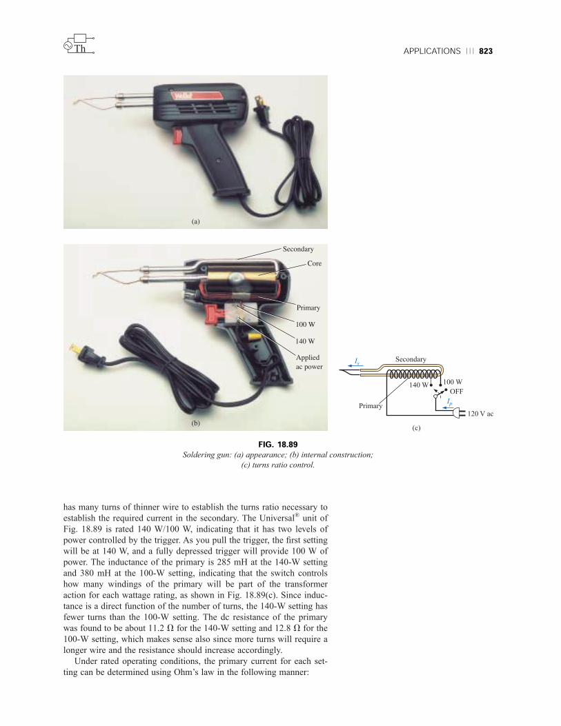
APPLICATIONS 823
has many turns of thinner wire to establish the turns ratio necessary to
establish the required current in the secondary. The Universal® unit of
Fig. 18.89 is rated 140 W/100 W, indicating that it has two levels of
power controlled by the trigger. As you pull the trigger, the first setting
will be at 140 W, and a fully depressed trigger will provide 100 W of
power. The inductance of the primary is 285 mH at the 140-W setting
and 380 mH at the 100-W setting, indicating that the switch controls
how many windings of the primary will be part of the transformer
action for each wattage rating, as shown in Fig. 18.89(c). Since induc-
tance is a direct function of the number of turns, the 140-W setting has
fewer turns than the 100-W setting. The dc resistance of the primary
was found to be about 11.2 V for the 140-W setting and 12.8 V for the
100-W setting, which makes sense also since more turns will require a
longer wire and the resistance should increase accordingly.
Under rated operating conditions, the primary current for each set-
ting can be determined using Ohm’s law in the following manner:
Th
!"
!"
#$$%&'(
)* $+,'-
./0 1
.00 1
2-&3)-4
5+-'
6'*+7()-4
(c)
Primary
IsSecondary
140 W 100 W
Ip
120 V ac
OFF
FIG. 18.89Soldering gun: (a) appearance; (b) internal construction;
(c) turns ratio control.

824 NETWORK THEOREMS (ac) Th
For 140 W,
Ip 5 V
P
p
5 1
1
4
2
0
0
W
V 5 1.17 A
For 100 W,
Ip 5 V
P
p
5 1
1
0
2
0
0
W
V 5 0.83 A
As expected, the current demand is more for the 140-W setting than
for the 100-W setting. Using the measured values of input inductance
and resistance for the 140-W setting, the equivalent circuit of Fig.
18.90(a) will result. Using the applied 60 Hz to determine the reactance
of the coil and then determining the total impedance seen by the pri-
mary will result in the following for the source current:
XL 5 2pf L 5 2p(60 Hz)(285 mH) 5 107.44 V
and ZT 5 R 1 j XL 5 11.2 V 1 j 107.44 V 5 108.02 V /84.05°
so that |Ip| 5 *Z
E
T
* 5 10
1
8
2
.
0
02
V
V 5 1.11 A
which is a close match with the rated level.
For the 100-W level of Fig. 18.90(b), the following analysis would
result:
XL 5 2pf L 5 2p(60 Hz)(380 mH) 5 143.26 V
and ZT 5 R 1 j XL 5 12.8 V 1 j 143.26 V 5 143.83 V /84.89°
so that |Ip| 5 *Z
E
T
* 5 14
1
3
2
.
0
83
V
V 5 0.83 A
which is a match to hundredths place with the value calculated from
rated conditions.
Removing the tip and measuring the primary and secondary voltages
resulted in 120 V/0.38 V for the 140-W setting and 120 V/0.31 V for the
100-W setting, respectively. Since the voltages of a transformer are
directly related to the turns ratio, the number of turns in the primary
(Np) to that of the secondary (Ns) can be estimated by the following for
each setting:
For 140 W,
N
N
p
s
5 0
1
.
2
3
0
8
V
V > 316
For 100 W,
N
N
p
s
5 0
1
.
2
3
0
1
V
V > 387
Looking at the photograph of Fig. 18.89(b), it would certainly appear
that there are 300 or more turns in the primary winding.
The currents of a transformer are related by the turns ratio in the fol-
lowing manner, permitting a calculation of the secondary currents for
each setting:
For 140 W,
Is 5 N
N
p
s
Ip 5 316(1.17 A) > 370 A
Rp 12.8 V
Lp 380 mH
+
120 V60 Hz
–
Ip
100 W
(b)
Rp 11.2 V
Lp 285 mH
+
120 V60 Hz
–
Ip
140 W
(a)
FIG. 18.90Equivalent circuits for the soldering iron of
Fig. 18.89(a): (a) at 140-W setting; (b) at
100-W setting.

APPLICATIONS 825
For 100 W,
Is 5 N
N
p
s
Ip 5 387(0.83 A) > 321 A
Quite clearly, the secondary current is much higher for the 140-W set-
ting. The resulting current levels are probably higher than you might
have expected, but keep in mind that the above analysis does not
include the effect of the reflected impedance from the secondary to the
primary that will reduce the primary current level (to be discussed in
Chapter 21). In addition, as the soldering tip heats up, its resistance
increases, further reducing the resulting current levels. Using an
Amp-Clamp®, the current in the secondary was found to exceed 300 A
when the power was first applied and the soldering tip was cold. How-
ever, as the tip heated up because of the high current levels, the current
through the primary dropped to about 215 A for the 140-W setting and
to 180 A for the 100-W setting. These high currents are part of the rea-
son that the lifetime of most soldering tips on soldering guns is about
20 hours. Eventually, the tip will simply begin to melt. Using these
levels of current and the given power rating, the resistance of the sec-
ondary can be approximated as follows:
For 140 W,
R 5 I
P2 5
(2
1
1
4
5
0
A
W
)2 > 3 mV
For 100 W,
R 5 I
P2 5
(1
1
8
0
0
0
A
W
)2 > 3 mV
which is as low as expected when you consider the cross-sectional
area of the secondary and the fact that the tip is a short section of
low-resistance, tin-plated copper.
One of the obvious advantages of the soldering gun versus the iron
is that the iron is off when you release the trigger, thus reducing energy
costs and extending the life of the tip. Applying dc current rather than
ac to develop a constant current would be impractical because the high
current demand would require a series of large batteries in parallel.
The above investigation was particularly interesting because of the
manner in which the constant current characteristic was established, the
levels of current established, and the excellent manner in which some of
the theory introduced in the text was verified.
Electronic SystemsOne of the blessings in the analysis of electronic systems is that the
superposition theorem can be applied so that the dc analysis and ac
analysis can be performed separately. The analysis of the dc system will
affect the ac response, but the analysis of each is a distinct, separate
process. Even though electronic systems have not been investigated in
this text, a number of important points can be made in the description
to follow that support some of the theory presented in this and recent
chapters, so inclusion of this description is totally valid at this point.
Consider the network of Fig. 18.91 with a transistor power amplifier, an
8-V speaker as the load, and a source with an internal resistance of 800 V.
Note that each component of the design was isolated by a color box
Th

826 NETWORK THEOREMS (ac)
to emphasize the fact that each component must be carefully weighed
in any good design.
As mentioned above, the analysis can be separated into a dc and an
ac component. For the dc analysis the two capacitors can be replaced by
an open-circuit equivalent (Chapter 10), resulting in an isolation of the
amplifier network as shown in Fig. 18.92. Given the fact that VBE will
be about 0.7 V dc for any operating transistor, the base current IB can
be found as follows using Kirchhoff’s voltage law:
IB 5 V
R
R
B
B 5
VCC
R
2
B
VBE 5
22 V
47
2
kV
0.7 V 5 453.2 mA
For transistors, the collector current IC is related to the base current
by IC 5 bIB, and
IC 5 bIB 5 (200)(453.2 mA) 5 90.64 mA
Finally, through Kirchhoff’s voltage law, the collector voltage (also
the collector-to-emitter voltage since the emitter is grounded) can be
determined as follows:
VC 5 VCE 5 VCC 2 ICRC 5 22 V 2 (90.64 mA)(100 V) 5 12.94 V
For the dc analysis, therefore,
IB 5 453.2 mA IC 5 90.64 mA VCE 5 12.94 V
which will define a point of dc operation for the transistor. This is an
important aspect of electronic design since the dc operating point will
have an effect on the ac gain of the network.
Now, using superposition, we can analyze the network from an ac
viewpoint by setting all dc sources to zero (replaced by ground connec-
tions) and replacing both capacitors by short circuits as shown in Fig.
18.93. Substituting the short-circuit equivalent for the capacitors is
valid because at 10 kHz (the midrange for human hearing response), the
reactance of the capacitor is determined by XC 5 1/2pfC 5 15.92 V
which can be ignored when compared to the series resistors at the
source and load. In other words, the capacitor has played the important
role of isolating the amplifier for the dc response and completing the
network for the ac response.
Th
Rs
RB 47 kV
RC 100 V
+
–
Vs 1V(p-p)
Source
CC
0.1 µF
Amplifier Load
0.1 µF
VCC = 22 V
β = 200
E
B
C
CC
RL 8 V
FIG. 18.91Transistor amplifier.
22 V
RB 47 kVRC 100 V
VCC
B
E
IB
+
–VBE
VCE
VCC 22 V
C
β = 200
–
+
IC
FIG. 18.92dc equivalent of the transistor network of
Fig. 18.91.
FIG. 18.93ac equivalent of the transistor network of
Fig. 18.91.
Rs
800 V
RB 47 kV
RC 100 V
B
E
C
RL 8 V
β = 200
Vs 1V(p-p)

APPLICATIONS 827Th
Redrawing the network as shown in Fig. 18.94(a) will permit an ac
investigation of its reponse. The transistor has now been replaced by an
equivalent network that will represent the behavior of the device. This
process will be covered in detail in your basic electronics courses. This
transistor configuration has an input impedance of 200 V and a current
source whose magnitude is sensitive to the base current in the input cir-
cuit and to the amplifying factor for this transistor of 200. The 47-kV
resistor in parallel with the 200-V input impedance of the transistor can
be ignored, so the input current Ii and base current Ib are determined by
Ii > Ib 5 Rs
V
1
s
Ri
5 5 1 V
1 k
(
V
p-p) 5 1 mA (p-p)
The collector current IC is then
IC 5 bIb 5 (200)(1 mA ( p-p)) 5 200 mA ( p-p)
and the current to the speaker is determined by the current divider rule
as follows:
IL 5 5 0.926IC 5 0.926(200 mA (p-p))
5 185.2 mA (p-p)
with the voltage across the speaker being
VL 5 2ILRL 5 2(185.2 mA ( p-p))(8 V) 5 21.48 V
The power to the speaker is then determined as follows:
Pspeaker 5 VLrms? ILrms
5 (VL( p-p)
8
)(IL( p-p)) 5
5 34.26 mW
which is relatively low. It would initially appear that the above was a
good design for distribution of power to the speaker because a majority
(1.48 V)(185.2 mA (p-p))
8
100 V(IC)100 V 1 8 V
1 V (p-p)800 V 1 200 V
(a)
RC 100 V
Rs
800 V
Ii
Vs 1V(p-p)
+
–
RL 8 VRi 200 VRB
B
E47 kΩ
I ≅ 0 A Ib βIb200Ib
C
IC
+
–IL
VL
Transistor equivalent circuit
(b)
100 V
8 V
100 V
Impedancematchingtransformer
+
– 200 mA
100 V
100 V100 mA
100 mA
VL
FIG. 18.94(a) Network of Fig. 18.93 following the substitution of the transistor equivalent
network; (b) effect of the matching transformer.

828 NETWORK THEOREMS (ac) Th
of the collector current went to the speaker. However, one must always
keep in mind that power is the product of voltage and current. A high
current with a very low voltage will result in a lower power level. In this
case, the voltage level is too low. However, if we introduce a matching
transformer that makes the 8-V resistive load “look like” 100 V as
shown in Fig. 18.94(b), establishing maximum power conditions, the
current to the load will drop to half of the previous amount because cur-
rent splits through equal resistors. But the voltage across the load will
increase to
VL 5 ILRL 5 (100 mA ( p-p))(100 V) 5 10 V ( p-p)
and the power level to
Pspeaker 5(VL( p-p)
8
)(IL( p-p))5
(10 V)(1
8
00 mA)5 125 mW
which is 3.6 times the gain without the matching transformer.
For the 100-V load, the dc conditions are unaffected due to the iso-
lation of the capacitor CC, and the voltage at the collector is 12.94 V as
shown in Fig. 18.95(a). For the ac response with a 100-V load, the out-
put voltage as determined above will be 10 V peak-to-peak (5 V peak)
as shown in Fig. 18.95(b). Note the out-of-phase relationship with the
input due to the opposite polarity of VL. The full response at the collec-
tor terminal of the transistor can then be drawn by superimposing the ac
response on the dc response as shown in Fig. 18.95(c) (another appli-
cation of the superposition theorem). In other words, the dc level sim-
ply shifts the ac waveform up or down and does not disturb its shape.
The peak-to-peak value remains the same, and the phase relationship is
unaltered. The total waveform at the load will include only the ac
response of Fig. 18.95(b) since the dc component has been blocked out
by the capacitor.
(a)
0 2TT t
12.94
VC (volts) dc
(c)
0 2TT t
vc (volts) ac + dc
12.94
17.94
7.94
(b)
0 2TT t
5
vc (volts) ac
–5
FIG. 18.95Collector voltage for the network of Fig. 18.91: (a) dc; (b) ac; (c) dc and ac.
The voltage at the source will appear as shown in Fig. 18.96(a),
while the voltage at the base of the transistor will appear as shown in
Fig. 18.96(b) because of the presence of the dc component.
A number of important concepts were presented in the above exam-
ple, with some probably leaving a question or two because of your lack
of experience with transistors. However, if nothing else is evident from
the above example, it should be the power of the superposition theorem
to permit an isolation of the dc and ac responses and the ability to com-
bine both if the total response is desired.
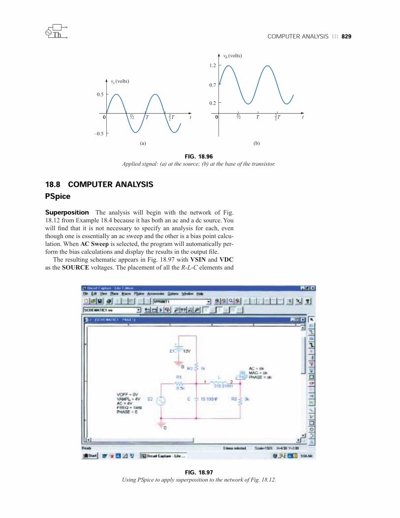
COMPUTER ANALYSIS 829Th
(a)
0 T t
vb (volts)
0.2
0 –T32
1.2
0.7
0 TT/2 t
vs (volts)
0.5
0
–0.5
–T32
(b)
T/2
FIG. 18.96Applied signal: (a) at the source; (b) at the base of the transistor.
18.8 COMPUTER ANALYSISPSpiceSuperposition The analysis will begin with the network of Fig.
18.12 from Example 18.4 because it has both an ac and a dc source. You
will find that it is not necessary to specify an analysis for each, even
though one is essentially an ac sweep and the other is a bias point calcu-
lation. When AC Sweep is selected, the program will automatically per-
form the bias calculations and display the results in the output file.
The resulting schematic appears in Fig. 18.97 with VSIN and VDC
as the SOURCE voltages. The placement of all the R-L-C elements and
FIG. 18.97Using PSpice to apply superposition to the network of Fig. 18.12.

830 NETWORK THEOREMS (ac) Th
the dc source should be quite straightforward at this point. For the ac
source, be sure to double-click on the source symbol to obtain the
Property Editor dialog box. Then set AC to 4 V, FREQ to 1 kHz,
PHASE to 0°, VAMPL to 4 V, and VOFF to 0 V. In each case choose
Name and Value under the Display heading so that we have a review
of the parameters on the screen. Also, be sure to Apply before exiting
the dialog box. Obtain the VPRINT1 option from the SPECIAL
library, place it as shown, and then double-click to obtain its Property
Editor. The parameters AC, MAG, and PHASE must then recieve the
OK listing, and Name and Value must be applied to each under
Display before you choose Apply and OK. The network is then ready
for simulation.
After you have selected the New Simulation Profile icon, the New
Simulation dialog box will appear in which SuperpositionAC is
entered as the Name. Following the selection of Create, the Simulation
Settings dialog box will appear in which AC Sweep/Noise is selected.
The Start and End Frequencies are both set at 1 kHz, and 1 is entered
for the Points/Decade request. Click OK, and then select the Run
PSpice key; the SCHEMATIC1 screen will result with an axis extend-
ing from 0.5 kHz to 1.5 kHz. Through the sequence Trace-Add Trace-
V(R3:1)-OK, the plot point appearing in the bottom of Fig. 18.98 will
result. Its value is slightly above the 2-V level and could be read as
2.05 V which compares very nicely with the hand-calculated solution of
2.06 V. The phase angle can be obtained from Plot-Add Plot to Window-
Trace-Add Trace-P(V(R3:1)) to obtain a phase angle close to 233°.
Additional accuracy can be added to the phase plot through the sequence
Plot-Axis Settings-Y Axis-User Defined 240d to 230d-OK, resulting
in the 232.5° reading of Fig. 18.98— again, very close to the hand cal-
FIG. 18.98The output results from the simulation of the network of Fig. 18.97.

COMPUTER ANALYSIS 831
culation of 232.74° of Example 18.4. Now this solution is fine for the
ac signal, but it tells us nothing about the dc component.
By exiting the SCHEMATIC1 screen, we obtain the Orcad Cap-
ture window on which PSpice can be selected followed by View Out-
put File. The result is the printout of Fig. 18.99 which has both the dc
and the ac solutions. The SMALL SIGNAL BIAS SOLUTION in-
cludes the nodes of the network and their dc levels. The node numbers
are defined under the netlist starting on line 30. In particular, note the
dc level of 3.6 V at node N00676 which is at the top of resistor R3 in
Fig. 18.97. Also note that the dc level of both ends of the inductor is the
same value because of the substitution of a short-circuit equivalent for
the inductor for dc analysis. The ac solution appears under the AC
ANALYSIS heading as 2.06 V at 232.66°, which again is a great ver-
ification of the results of Example 18.4.
Th
FIG. 18.99The output file for the dc (SMALL SIGNAL BIAS SOLUTION) and
AC ANALYSIS for the network of Fig. 18.97.
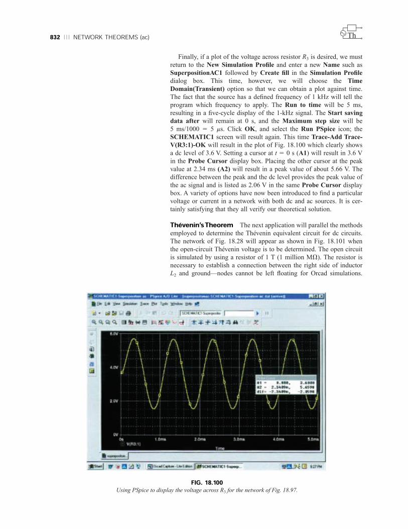
832 NETWORK THEOREMS (ac)
Finally, if a plot of the voltage across resistor R3 is desired, we must
return to the New Simulation Profile and enter a new Name such as
SuperpositionAC1 followed by Create fill in the Simulation Profile
dialog box. This time, however, we will choose the Time
Domain(Transient) option so that we can obtain a plot against time.
The fact that the source has a defined frequency of 1 kHz will tell the
program which frequency to apply. The Run to time will be 5 ms,
resulting in a five-cycle display of the 1-kHz signal. The Start saving
data after will remain at 0 s, and the Maximum step size will be
5 ms/1000 5 5 ms. Click OK, and select the Run PSpice icon; the
SCHEMATIC1 screen will result again. This time Trace-Add Trace-
V(R3:1)-OK will result in the plot of Fig. 18.100 which clearly shows
a dc level of 3.6 V. Setting a cursor at t 5 0 s (A1) will result in 3.6 V
in the Probe Cursor display box. Placing the other cursor at the peak
value at 2.34 ms (A2) will result in a peak value of about 5.66 V. The
difference between the peak and the dc level provides the peak value of
the ac signal and is listed as 2.06 V in the same Probe Cursor display
box. A variety of options have now been introduced to find a particular
voltage or current in a network with both dc and ac sources. It is cer-
tainly satisfying that they all verify our theoretical solution.
Thévenin’s Theorem The next application will parallel the methods
employed to determine the Thévenin equivalent circuit for dc circuits.
The network of Fig. 18.28 will appear as shown in Fig. 18.101 when
the open-circuit Thévenin voltage is to be determined. The open circuit
is simulated by using a resistor of 1 T (1 million MV). The resistor is
necessary to establish a connection between the right side of inductor
L2 and ground—nodes cannot be left floating for Orcad simulations.
Th
FIG. 18.100Using PSpice to display the voltage across R3 for the network of Fig. 18.97.

COMPUTER ANALYSIS 833Th
FIG. 18.101Using PSpice to determine the open-circuit Thévenin voltage.
Since the magnitude and the angle of the voltage are required,
VPRINT1 is introduced as shown in Fig 18.101. The simulation was an
AC Sweep simulation at 1 kHz, and when the Orcad Capture window
was obtained, the results appearing in Fig. 18.102 were taken from the
listing resulting from the PSpice-View Output File. The magnitude of
the Thévenin voltage is 5.187 V to compare with the 5.08 V of Exam-
ple 18.8, while the phase angle is 277.13° to compare with the
277.09° of the same example—excellent results.
FIG. 18.102The output file for the open-circuit Thévenin voltage for the network
of Fig. 18.101.

834 NETWORK THEOREMS (ac) Th
FIG. 18.103Using PSpice to determine the short-circuit current.
Next, the short-circuit current will be determined using IPRINT as
shown in Fig. 18.103, to permit a determination of the Thévenin imped-
ance. The resistance Rcoil of 1 mV had to be introduced because induc-
tors cannot be treated as ideal elements when using PSpice; they must
all show some series internal resistance. Note that the short-circuit
current will pass directly through the printer symbol for IPRINT. Inci-
dentally, there is no need to exit the SCHEMATIC1 developed above
to determine the Thévenin voltage. Simply delete VPRINT and R3,
and insert IPRINT. Then run a new simulation to obtain the results of
Fig. 18.104. The magnitude of the short-circuit current is 0.936 A at an
angle of 2108°. The Thévenin impedance is then defined by
ZTh 5 5 5 5.54 V /30.87°
which is an excellent match with 5.49 V
/32.36° obtained in Example 18.8.
5.187 V /277.13°0.936 A /2108.0°
EThIsc
VCVS The last application of this section will be to verify the results
of Example 18.12 and to gain some practice using controlled (depen-
dent) sources. The network of Fig. 18.50, with its voltage-controlled
voltage source (VCVS), will have the schematic appearance of Fig.
18.105. The VCVS appears as E in the ANALOG library, with the volt-
age E1 as the controlling voltage and E as the controlled voltage. In the
Property Editor dialog box, the GAIN must be changed to 20 while

COMPUTER ANALYSIS 835
the rest of the columns can be left as is. After Display-Name and
Value, Apply can be selected and the dialog box exited to result in
GAIN 5 20 near the controlled source. Take particular note of the sec-
ond ground inserted near E to avoid a long wire to ground that might
overlap other elements. For this exercise the current source ISRC will
be used because it has an arrow in its symbol, and frequency is not
Th
FIG. 18.104The output file for the short-circuit current for the network of Fig. 18.103.
FIG. 18.105Using PSpice to determine the open-circuit Thévenin voltage for the
network of Fig. 18.50.

836 NETWORK THEOREMS (ac)
important for this analysis since there are only resistive elements pre-
sent. In the Property Editor dialog box, the AC level is set to 5 mA,
and the DC level to 0 A; both were displayed using Display-Name and
value. VPRINT1 is set up as in past exercises. The resistor Roc (open
circuit) was given a very large value so that it would appear as an open
circuit to the rest of the network. VPRINT1 will provide the open cir-
cuit Thévenin voltage between the points of interest. Running the sim-
ulation in the AC Sweep mode at 1 kHz will result in the output file
appearing in Fig. 18.106, revealing that the Thévenin voltage is 210 V
/0°. Substituting the numerical values of this example into the equa-
tion obtained in Example 18.12 confirms the result:
ETh 5 (1 1 m)IR1 5 (1 1 20) (5 mA /0°)(2 kV)
5 210 V/0°
Th
FIG. 18.106The output file for the open-circuit Thévenin voltage for the network
of Fig. 18.105.
Next, the short-circuit current must be determined using the IPRINT
option. Note in Fig. 18.107 that the only difference between this net-
work and that of Fig. 18.106 is the replacement of Roc with IPRINT
and the removal of VPRINT1. There is therefore no need to completely
“redraw” the network. Just make the changes and run a new simulation.
The result of the new simulation as shown in Fig. 18.108 is a current of
5 mA at an angle of 0°.
The ratio of the two measured quantities will result in the Thévenin
impedance:
ZTh 5 5 5 5 42 kV
which also matches the longhand solution of Example 18.12:
ZTh 5 (1 1 m)R1 5 (1 1 20)2 kV 5 (21)2 kV 5 42 kV
The analysis of the full transistor equivalent network of Fig. 18.56
with two controlled sources can be found in the PSpice section of
Chapter 26.
210 V /0°5 mA /0°
EThIsc
EocIsc

COMPUTER ANALYSIS 837Th
FIG. 18.108The output file for the short-circuit current for the network of Fig. 18.107.
FIG. 18.107Using PSpice to determine the short-circuit current for the network
of Fig. 18.50.

838 NETWORK THEOREMS (ac) Th
PROBLEMSSECTION 18.2 Superposition Theorem
1. Using superposition, determine the current through the
inductance XL for each network of Fig. 18.109.
R 3 V
+
E1 = 30 V ∠ 30°–
ILXC 6 V
+
E2 = 60 V ∠ 10°–
XL 8 V
(a)
I = 0.3 A ∠ 60°
ILXC 5 V
+
E = 10 V ∠ 0°–
XL 8 V
(b)
FIG. 18.109Problem 1.
*2. Using superposition, determine the current IL for each
network of Fig. 18.110.
R 1 V
+
E1 = 20 V ∠ 0°–
IL
+
E2 = 120 V ∠ 0°–
XL 3 V
(a)
IL
XC27 V
I = 0.5 A ∠ 60°
R
4 V
+
E = 10 V ∠ 90°–
XL
3 V
(b)
I = 0.6 A ∠ 120°
XC1
6 V
FIG. 18.110Problem 2.
*3. Using superposition, find the sinusoidal expression for
the current i for the network of Fig. 18.111.
4. Using superposition, find the sinusoidal expression for
the voltage vC for the network of Fig. 18.112.
FIG. 18.111Problems 3, 15, 30, and 42.
R1 6 V
4 V
XL
2 VXCE2 = 4 V
+
–
+
–
E1 = 10 V ∠0°R2 8 V
i
R2
3 V
1 VXC
+
–
4 A ∠0°I vC
R1
6 V
12 V
FIG. 18.112Problems 4, 16, 31, and 43.

PROBLEMS 839Th
R 20 kV
+–E = 10 V ∠ 0°
10 kVXL
IL
hI
I = 2 mA ∠ 0°
FIG. 18.114Problems 6 and 20.
7. Using superposition, for the network of Fig. 18.115,
determine the voltage VL (m 5 20).
FIG. 18.115Problems 7, 21, and 35.
R2 4 kVV = 2 V ∠ 0° I = 2 mA ∠ 0°mV
–
+–
+
R1
5 kV
XC
1 kV
–
+
VL
*5. Using superposition, find the current I for the network of
Fig. 18.113.
FIG. 18.113Problems 5, 17, 32, and 44.
R1 10 kV
5 kVXC
+–
I = 5 mA ∠ 0°R2 5 kV
E = 20 V ∠ 0°
5 kVXL
I
6. Using superposition, determine the current IL (h 5 100)
for the network of Fig. 18.114.

840 NETWORK THEOREMS (ac) Th
*8. Using superposition, determine the current IL for the net-
work of Fig. 18.116 (m 5 20; h 5 100).
V = 10 V ∠ 0°
mV– +
–
+
R1 20 kV
R2
5 kV
5 kVXL
IL
I = 1 mA ∠ 0°
hI
FIG. 18.116Problems 8, 22, and 36.
*9. Determine VL for the network of Fig. 18.117 (h 5 50).
RL 2 kV
+
–
E = 20 V ∠ 53° VLhI
+
–
I
R1 = 2 kV
FIG. 18.117Problems 9 and 23.
R2 5 kV
+ –
I1 = 1 mA ∠ 0°
I
20V
R1 2 kV I2 = 2 mA ∠ 0°+
–V
FIG. 18.118Problems 10, 24, and 38.
*10. Calculate the current I for the network of Fig. 18.118.

Th PROBLEMS 841
*13. Find the Thévenin equivalent circuit for the portions of
the networks of Fig. 18.121 external to the elements
between points a and b.
I = 0.1 A ∠ 0°
XL
20 VR1
20 V
XC 32 V
a
b
(a)
+
–
E = 50 V ∠ 0°
XC2
2 V
R1
6 V
XL
4 V
a
b
(b)
R2 = 68 V
XC1
8 VR2
10 V
FIG. 18.121Problems 13 and 27.
I
R2 2 V
+
R1 10 VVx
–
10 V∠0°
–
E1
+
–
4Vx
+5 A∠0°
–
Vs
+
FIG. 18.119Problem 11.
11. Find the voltage Vs for the network of Fig. 18.119.
+
–
E = 100 V ∠ 0° XL
3 V
R
4 V XC 2 V
a
b
(a)
+
–
E = 20 V ∠ 0°
XL
2 kV
R
6 kV
XC 3 kV
a
b
(b)
RL
FIG. 18.120Problems 12 and 26.
SECTION 18.3 Thévenin’s Theorem12. Find the Thévenin equivalent circuit for the portions of
the networks of Fig. 18.120 external to the elements
between points a and b.

842 NETWORK THEOREMS (ac) Th
*15. a. Find the Thévenin equivalent circuit for the network
external to the resistor R2 in Fig. 18.111.
b. Using the results of part (a), determine the current i of
the same figure.
16. a. Find the Thévenin equivalent circuit for the network
external to the capacitor of Fig. 18.112.
b. Using the results of part (a), determine the voltage VC
for the same figure.
*17. a. Find the Thévenin equivalent circuit for the network
external to the inductor of Fig. 18.113.
b. Using the results of part (a), determine the current I of
the same figure.
18. Determine the Thévenin equivalent circuit for the net-
work external to the 5-kV inductive reactance of Fig.
18.123 (in terms of V).
19. Determine the Thévenin equivalent circuit for the net-
work external to the 4-kV inductive reactance of Fig.
18.124 (in terms of I).
–
+
R1 10 kV
R2 10 kV XL 5 kV
XC
1 kV
Th
20V
FIG. 18.123Problems 18 and 33.
*14. Find the Thévenin equivalent circuit for the portions of
the networks of Fig. 18.122 external to the elements
between points a and b.
(a)
–
+
E1 = 120 V ∠ 0°
R
10 V
XC
8 V
XL 8 VI =0.5 A ∠ 60° ZL
a
b
R2
10 V
XC
10 V
a
b
I = 0.6 A ∠ 90° E = 20 V ∠ 40°–
+
R1 9 VI2 =0.8 ∠ 60°
(b)
FIG. 18.122Problems 14 and 28.
R1 40 kV R2 5 kV
Th
XL 4 kV100I
XC
0.2 kV
FIG. 18.124Problems 19 and 34.

Th PROBLEMS 843
20. Find the Thévenin equivalent circuit for the network
external to the 10-kV inductive reactance of Fig. 18.114.
21. Determine the Thévenin equivalent circuit for the net-
work external to the 4-kV resistor of Fig. 18.115.
*22. Find the Thévenin equivalent circuit for the network
external to the 5-kV inductive reactance of Fig. 18.116.
*23. Determine the Thévenin equivalent circuit for the net-
work external to the 2-kV resistor of Fig. 18.117.
*24. Find the Thévenin equivalent circuit for the network
external to the resistor R1 of Fig. 18.118.
*25. Find the Thévenin equivalent circuit for the network to
the left of terminals a-a9 of Fig. 18.125.
SECTION 18.4 Norton’s Theorem26. Find the Norton equivalent circuit for the network exter-
nal to the elements between a and b for the networks of
Fig. 18.120.
27. Find the Norton equivalent circuit for the network exter-
nal to the elements between a and b for the networks of
Fig. 18.121.
28. Find the Norton equivalent circuit for the network exter-
nal to the elements between a and b for the networks of
Fig. 18.122.
*29. Find the Norton equivalent circuit for the portions of the
networks of Fig. 18.126 external to the elements between
points a and b.
R1 2 kV
+
8 V∠0°5Ix R3 3.3 kV
R2
1 kV
E–
Thévenin
Ix
a
a
FIG. 18.125Problem 25.
–
+R2 9 V
R1
6 V
XC 12 Vb
a
XL
8 V
E I2 = 0.4 A ∠ 20°
XL
4 V
–
+
E1 = 120 V ∠ 30° R2 8 V
–
+
E2 = 108 V ∠ 0°
R1 = 3 V XC 8 V
R3 68 V
R4 40 V
a
b
ZL20 V ∠ 0°
(a) (b)
FIG. 18.126Problem 29.
*30. a. Find the Norton equivalent circuit for the network
external to the resistor R2 in Fig. 18.111.
b. Using the results of part (a), determine the current I of
the same figure.
*31. a. Find the Norton equivalent circuit for the network
external to the capacitor of Fig. 18.112.
b. Using the results of part (a), determine the voltage VC
for the same figure.
*32. a. Find the Norton equivalent circuit for the network
external to the inductor of Fig. 18.113.
b. Using the results of part (a), determine the current I of
the same figure.
33. Determine the Norton equivalent circuit for the network
external to the 5-kV inductive reactance of Fig. 18.123.

844 NETWORK THEOREMS (ac) Th
34. Determine the Norton equivalent circuit for the network
external to the 4-kV inductive reactance of Fig. 18.124.
35. Find the Norton equivalent circuit for the network exter-
nal to the 4-kV resistor of Fig. 18.115.
*36. Find the Norton equivalent circuit for the network exter-
nal to the 5-kV inductive reactance of Fig. 18.116.
*37. For the network of Fig. 18.127, find the Norton equiva-
lent circuit for the network external to the 2-kV resistor.
*38. Find the Norton equivalent circuit for the network exter-
nal to the I1 current source of Fig. 18.118.
SECTION 18.5 Maximum Power Transfer Theorem39. Find the load impedance ZL for the networks of Fig.
18.128 for maximum power to the load, and find the
maximum power to the load.
R1 1 kV V R2 3 kV R4 2 kVI = 2 mA ∠ 0°
R3
4 kV
– +
–
+
µ( = 20)µV
FIG. 18.127Problem 37.
–
+
R1
3 V
XC 6 V
XL
4 V
E = 120 V ∠ 0° ZL
(a)
XL
4 V
I = 2 A ∠ 30°
ZL
(b)
R2 2 VR1 3 V
FIG. 18.128Problem 39.

Th PROBLEMS 845
*40. Find the load impedance ZL for the networks of Fig.
18.129 for maximum power to the load, and find the
maximum power to the load.
–
+
R
10 V
XC15 V
XL
4 V
E = 60 V ∠ 60°
(a)
XL1
4 V
ZL
(b)
R2 12 VR1 3 V
ZL
XC26 V
9 V
XC 8 V
E1 = 100 V ∠ 0° E2 = 200 V ∠ 90°
XL2
–
+
–
+
FIG. 18.129Problem 40.
41. Find the load impedance RL for the network of Fig.
18.130 for maximum power to the load, and find the
maximum power to the load.
–
+
R1 1 kV R2 40 kV RL
I
50I
E = 1 V ∠ 0°
FIG. 18.130Problem 41.
*42. a. Determine the load impedance to replace the resistor
R2 of Fig. 18.111 to ensure maximum power to the
load.
b. Using the results of part (a), determine the maximum
power to the load.
*43. a. Determine the load impedance to replace the capaci-
tor XC of Fig. 18.112 to ensure maximum power to the
load.
b. Using the results of part (a), determine the maximum
power to the load.
*44. a. Determine the load impedance to replace the inductor
XL of Fig. 18.113 to ensure maximum power to the
load.
b. Using the results of part (a), determine the maximum
power to the load.
45. a. For the network of Fig. 18.131, determine the value of
RL that will result in maximum power to the load.
b. Using the results of part (a), determine the maximum
power delivered.
–
+
R
2 kVLOAD
RL
XL 2 kV
XC
2 kVE = 50 V ∠ 0°
FIG. 18.131Problem 45.

846 NETWORK THEOREMS (ac) Th
*46. a. For the network of Fig. 18.132, determine the level of
capacitance that will ensure maximum power to the
load if the range of capacitance is limited to 1 nF to
5 nF.
b. Using the results of part (a), determine the value of RL
that will ensure maximum power to the load.
c. Using the results of parts (a) and (b), determine the
maximum power to the load.
–
+RL
E = 2 V ∠ 0° R 1 kV C 3.98 nF
C (1 – 5 nF)
LOAD
31.8 mH
L
f = 10 kHz
FIG. 18.132Problem 46.
SECTION 18.6 Substitution, Reciprocity, andMillman’s Theorems47. For the network of Fig. 18.133, determine two equivalent
branches through the substitution theorem for the branch
a-b.
R1 4 kV R2 8 kV
a
b
I = 4 mA ∠ 0°
FIG. 18.133Problem 47.
–
+
R1
1 kV
R2
8 kV
R4
11 kV
R3
4 kV
R5
6 kVE = 20 V ∠ 0°
I
R1
1 kV
R2
8 kV
R4
11 kV
R3
4 kV
R5 = 6 kV
E = 20 V ∠ 0°
I
(a) (b)
–
+
FIG. 18.134Problem 48.
48. a. For the network of Fig. 18.134(a), find the current I.
b. Repeat part (a) for the network of Fig. 18.134(b).
c. Do the results of parts (a) and (b) compare?

Th GLOSSARY 847
49. Using Millman’s theorem, determine the current through
the 4-kV capacitive reactance of Fig. 18.135.
–
+
XL 4 kVR1 2 kVIC
4 kV
E1 = 100 V ∠ 0° E2 = 50 V ∠ 360°XC
–
+
FIG. 18.135Problem 49.
SECTION 18.8 Computer AnalysisPSpice or Electronics Workbench50. Apply superposition to the network of Fig. 18.6. That is,
determine the current I due to each source, and then find
the resultant current.
*51. Determine the current IL for the network of Fig. 18.21
using schematics.
*52. Using schematics, determine V2 for the network of Fig.
18.56 if Vi 5 1 V /0°, R1 5 0.5 kV, k1 5 3 3 1024,
k2 5 50, and R2 5 20 kV.
*53. Find the Norton equivalent circuit for the network of Fig.
18.75 using schematics.
*54. Using schematics, plot the power to the R-C load of Fig.
18.88 for values of RL from 1 V to 10 V.
Programming Language (C11, QBASIC, Pascal, etc.)55. Given the network of Fig. 18.1, write a program to deter-
mine a general solution for the current I using superposi-
tion. That is, given the reactance of the same network ele-
ments, determine I for voltage sources of any magnitude
but the same angle.
56. Given the network of Fig. 18.23, write a program to
determine the Thévenin voltage and impedance for any
level of reactance for each element and any magnitude of
voltage for the voltage source. The angle of the voltage
source should remain at zero degrees.
57. Given the configuration of Fig. 18.136, demonstrate that
maximum power is delivered to the load when XC 5 XL
by tabulating the power to the load for XC varying from
0.1 kV to 2 kV in increments of 0.1 kV.
R2 2 kV
R1
2 kV
XC
ZL
1 kV
XL
E = 10 V ∠ 0°
+
–
FIG. 18.136Problem 57.
GLOSSARYMaximum power transfer theorem A theorem used to
determine the load impedance necessary to ensure maxi-
mum power to the load.
Millman’s theorem A method employing voltage-to-current
source conversions that will permit the determination of
unknown variables in a multiloop network.
Norton’s theorem A theorem that permits the reduction of
any two-terminal linear ac network to one having a single
current source and parallel impedance. The resulting config-
uration can then be employed to determine a particular cur-
rent or voltage in the original network or to examine the
effects of a specific portion of the network on a particular
variable.
Reciprocity theorem A theorem stating that for single-
source networks, the magnitude of the current in any branch
of a network, due to a single voltage source anywhere else
in the network, will equal the magnitude of the current
through the branch in which the source was originally
located if the source is placed in the branch in which the
current was originally measured.
Substitution theorem A theorem stating that if the voltage
across and current through any branch of an ac bilateral net-