
Behavioral models of I/O ports from measured transient waveforms
19
IEEE TRANSACTIONS ON I NSTRUMENTATION AND MEASUREMENT REVISED MANUSCRIPT:J UN 10, 2002 FINAL MANUSCRIPT:SEP . 30, 2002 Behavioral Models of I/O Ports from Measured Transient Waveforms Igor S. Stievano (Member), Ivan A. Maio (Member), Flavio G. Canavero (Senior Member), Politecnico di Torino, Dip. di Elettronica C. Duca degli Abruzzi 24, 10129 Torino, ITALY Index Terms Digital integrated circuits, I/O ports, circuit modeling, macromodeling, system identification, radial basis function models, signal integrity, electromagnetic compatibility. Corresponding Author Igor S. Stievano Politecnico di Torino, Dip. Elettronica C. Duca degli Abruzzi 24, 10129 Torino, ITALY Phone: (+39) 011-5644184, Fax: (+39) 011-5644099, E-mail: [email protected]
Transcript of Behavioral models of I/O ports from measured transient waveforms
IEEE TRANSACTIONS ON INSTRUMENTATION AND MEASUREMENT
REVISED MANUSCRIPT: JUN 10, 2002
FINAL MANUSCRIPT: SEP. 30, 2002
Behavioral Models of I/O Ports fromMeasured Transient Waveforms
Igor S. Stievano (Member), Ivan A. Maio (Member), Flavio G. Canavero (Senior Member),
Politecnico di Torino, Dip. di Elettronica C. Duca degli Abruzzi 24, 10129 Torino, ITALY
Index Terms
Digital integrated circuits, I/O ports, circuit modeling, macromodeling, system
identification, radial basis function models, signal integrity, electromagnetic compatibility.
Corresponding Author
Igor S. Stievano
Politecnico di Torino, Dip. Elettronica
C. Duca degli Abruzzi 24, 10129 Torino, ITALY
Phone: (+39) 011-5644184, Fax: (+39) 011-5644099, E-mail: [email protected]
I. S. STIEVANO, I. A. MAIO, F. G. CANAVERO, BEHAVIORAL MODELS OF I/O PORTS. . . 1
Abstract
This paper addresses the development of accurate and efficient behavioral models of digital IC ports from
measured transient responses. The proposed approach is based on the estimation of parametric models from
port voltage and current waveforms. The modeling process is described and applied to the modeling of output
ports. Its feasibility is demonstrated by the identification of a real device from actual measurements, and by the
comparison of the predicted device response with the measured one.
Keywords
Circuit modeling, Digital integrated circuits, Electromagnetic compatibility, Identification
I. INTRODUCTION
Extended band behavioral models of digital Integrated Circuit (IC) ports are key ele-
ments for the simulation of sensitive Signal Integrity (SI) and ElectroMagnetic Compatibility
(EMC) effects in fast digital circuits. The most common approach to behavioral modeling of
IC ports is via simplified equivalent circuits, because they allow physical insight and facili-
tate the implementation of models. An important example of the equivalent circuit approach
to behavioral modeling is the widely adopted Input/output Buffer Information Specification
(IBIS) [1]. IBIS offers high numerical efficiency, large data library and commercial software
tools handling models and complex modeling problems.
The equivalent circuit approach to behavioral modeling, however, has also inherent lim-
itations. In fact, the estimation of model parameters is readily done by means of virtual
measurements only (i.e., if the transistor-level model of the device is available). In addition,
the circuit structure defining the model decides a-priori the physical effects to be considered,
leaving no possibilities to reproduce other effects inherent to a specific device.
An alternative approach to behavioral modeling of IC ports is their identification by means
of nonlinear dynamic parametric models. In this approach, the parameters of a suitable model
are estimated from the voltage and current waveforms measured at the device ports. The
modeled device is considered as a black-box, i.e., in principle, no knowledge of the internal
structure is required and the modeling information is completely contained in the device ex-
ternal responses. Owing to this feature, parametric models can be effectively estimated from

I. S. STIEVANO, I. A. MAIO, F. G. CANAVERO, BEHAVIORAL MODELS OF I/O PORTS. . . 2
measured transient responses or from simulated responses computed for detailed reference
transistor-level models. Besides, since the structure of the parametric models is partially se-
lected by the identification process itself, they automatically include all significant physical
effects relating input and output waveforms.
In this paper, we shortly review the modeling of IC ports via the identification approach
and apply it to the modeling of an IC output port from measured transient waveforms, thereby
demonstrating the feasibility and advantages of the method. The process for the construction
of IC port parametric models is outlined in Section II and the modeling example involving a
real device is described in Section III.
II. MODELING PROCESS
Since in system level SI and EMC simulations, the aim is the prediction of signals on
board and on cables, for a specified logic activity of their drivers, the internal operation of
ICs is neglected. Thus, the device ports act as receivers or signal pattern generators loading
the interconnect. The required IC models, therefore, are relations between the voltages and
the currents of the IC ports for a known internal logical activity. The generic model is a
constitutive relation of the form
����������� �������������������(1)
where�������
and�������
are the port current and voltage, respectively,
is a nonlinear dynamic
operator and�������
is an extra input needed to specify the port transitions.
In the identification approach addressed in this paper, the operator
in (1) is a (discrete-
time) nonlinear parametric model and its construction relies on the well established theory
of system identification [2]. For the problem at hand, the complete modeling process can be
divided into three parts: (A) the selection of a suitable parametric model; (B) the estimation
of the model parameters; (C) the implementation of the model as a subcircuit of a circuit
simulation environment. In this section, the above modeling process is detailed for the gen-
eral case of output ports. Input ports can be handled by a simplified version of the process
for output ports, and are explicitly addressed in [3].
I. S. STIEVANO, I. A. MAIO, F. G. CANAVERO, BEHAVIORAL MODELS OF I/O PORTS. . . 3
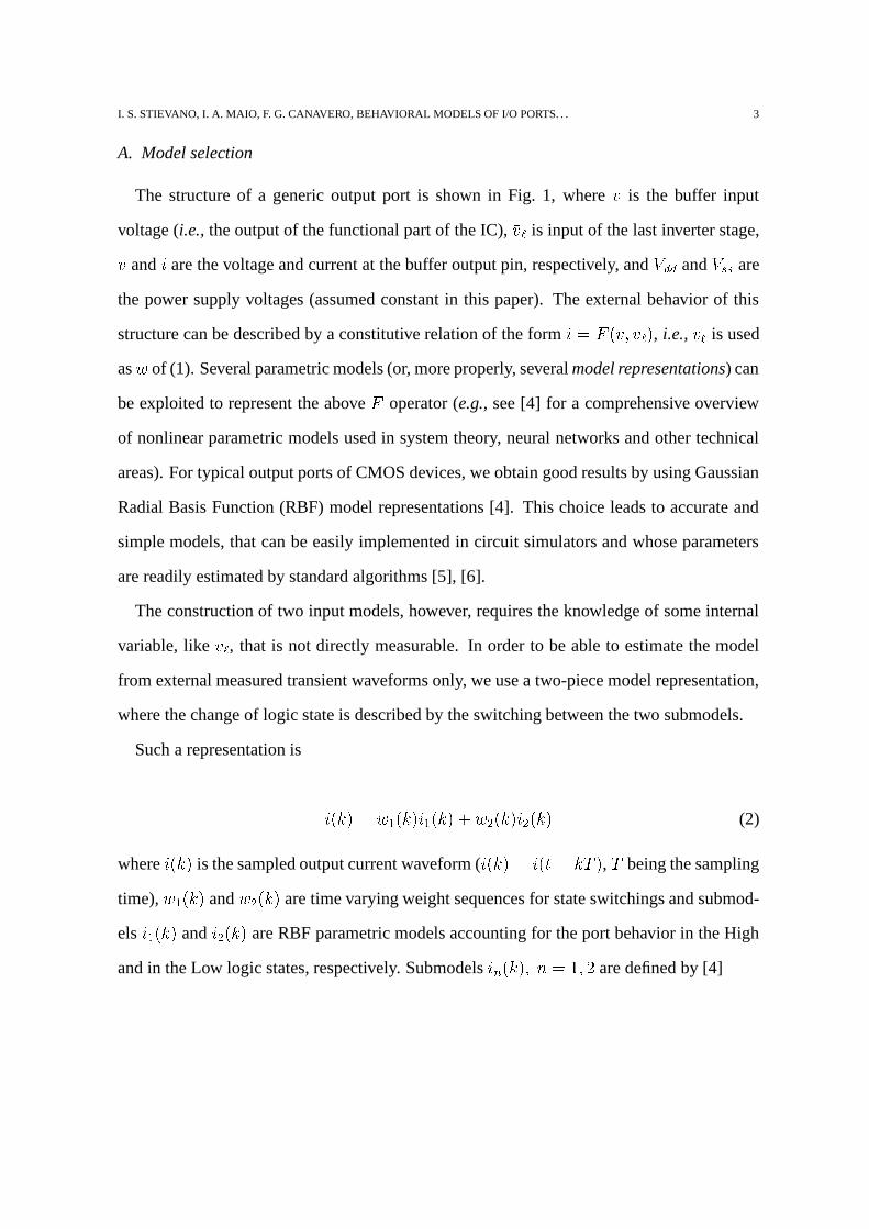
A. Model selection
The structure of a generic output port is shown in Fig. 1, where ��
is the buffer input
voltage (i.e., the output of the functional part of the IC), �� � is input of the last inverter stage,
�and
�are the voltage and current at the buffer output pin, respectively, and
�����and
�����are
the power supply voltages (assumed constant in this paper). The external behavior of this
structure can be described by a constitutive relation of the form� � �� � �
�� � � , i.e., �
� � is used
as�
of (1). Several parametric models (or, more properly, several model representations) can
be exploited to represent the above
operator (e.g., see [4] for a comprehensive overview
of nonlinear parametric models used in system theory, neural networks and other technical
areas). For typical output ports of CMOS devices, we obtain good results by using Gaussian
Radial Basis Function (RBF) model representations [4]. This choice leads to accurate and
simple models, that can be easily implemented in circuit simulators and whose parameters
are readily estimated by standard algorithms [5], [6].
The construction of two input models, however, requires the knowledge of some internal
variable, like �� � , that is not directly measurable. In order to be able to estimate the model
from external measured transient waveforms only, we use a two-piece model representation,
where the change of logic state is described by the switching between the two submodels.
Such a representation is
���� ��� �� �� � �� �� � � ��� �� � ��� �� �(2)
where���� �
is the sampled output current waveform (���� ��� ���������� �
,�
being the sampling
time),�� �� �
and��� �� �
are time varying weight sequences for state switchings and submod-
els�� �� �
and��� �� �
are RBF parametric models accounting for the port behavior in the High
and in the Low logic states, respectively. Submodels��� �� ����� ��� ���
are defined by [4]
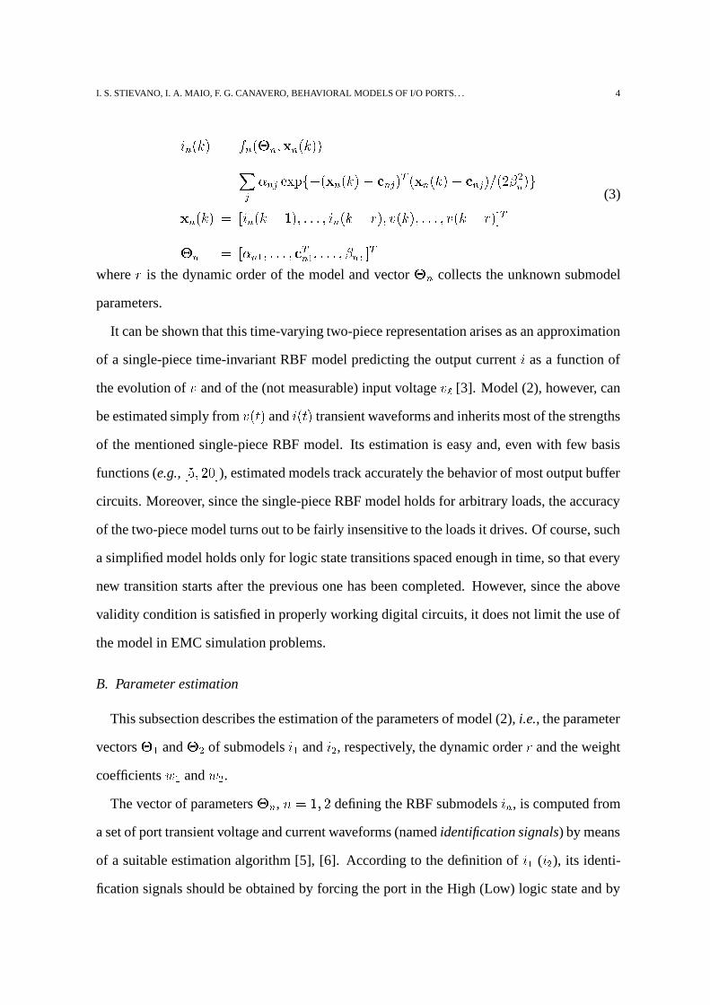
I. S. STIEVANO, I. A. MAIO, F. G. CANAVERO, BEHAVIORAL MODELS OF I/O PORTS. . . 4
� � �� � � � � ��� � ����� �� �������� � ���� ������ ����� �� � ���
����� ����� �� � ���
����� ����� �� ���
��� �� � ��� � � �� � � ���! ! ! ��� � �� �#"�������� ���! ! ! ������ �#"
�%$ �� � ��� � �! ! ! � � � � �! ! ! �&� � ��$ �
(3)
where
"is the dynamic order of the model and vector
� �collects the unknown submodel
parameters.
It can be shown that this time-varying two-piece representation arises as an approximation
of a single-piece time-invariant RBF model predicting the output current�
as a function of
the evolution of�
and of the (not measurable) input voltage �� � [3]. Model (2), however, can
be estimated simply from�������
and�������
transient waveforms and inherits most of the strengths
of the mentioned single-piece RBF model. Its estimation is easy and, even with few basis
functions (e.g.,� ' ���)(�$
), estimated models track accurately the behavior of most output buffer
circuits. Moreover, since the single-piece RBF model holds for arbitrary loads, the accuracy
of the two-piece model turns out to be fairly insensitive to the loads it drives. Of course, such
a simplified model holds only for logic state transitions spaced enough in time, so that every
new transition starts after the previous one has been completed. However, since the above
validity condition is satisfied in properly working digital circuits, it does not limit the use of
the model in EMC simulation problems.
B. Parameter estimation
This subsection describes the estimation of the parameters of model (2), i.e., the parameter
vectors�
and� �
of submodels�
and���
, respectively, the dynamic order
"and the weight
coefficients�
and���
.
The vector of parameters� �
,� ��� ���
defining the RBF submodels���
, is computed from
a set of port transient voltage and current waveforms (named identification signals) by means
of a suitable estimation algorithm [5], [6]. According to the definition of�
(���
), its identi-
fication signals should be obtained by forcing the port in the High (Low) logic state and by
I. S. STIEVANO, I. A. MAIO, F. G. CANAVERO, BEHAVIORAL MODELS OF I/O PORTS. . . 5
recording the port current response (submodel output) to a voltage signal (submodel input).
The design of the input identification signal, i.e., the voltage signal stimulating the output
port, is a key point of the modeling process. Such a signal should be able to excite every
possible dynamic behavior of the modeled port taking place in the frequency bandwidth and
in the current and voltage ranges of interest [2]. For linear systems, this is accomplished
by using white noise or pseudorandom binary signals as input identification signals. For
nonlinear systems, instead, only qualitative guidelines are available for the design of input
identification signals, leading to noisy multilevel signals. Taking into account that the in-
put identification waveform must be obtained in a real measurement setup, we look for the
simplest input identification signal ensuring successful estimation. Our optimum choice are
voltage waveforms composed of three to six level transitions spanning the range of operation
voltages, i.e.,� � ��� ��� � � ��� � � $
, where
�is the accepted overvoltage. The flat parts of the
waveform should last enough time to allow the port to reach steady state operation, whereas
the edges are linear and have rise/fall times comparable to the switching times of the port.
Once the identification signals have been obtained, the estimation of the model parameters
requires the knowledge of the model dynamic order
", that defines the size of the regressor
vectors of (3). The dynamic order is an inherent property of the modeled system and it
should be estimated a-priori directly from the system response [7]. We carried out a-priori
dynamic order estimations for several example CMOS output ports and we always found
"
values in the range��� �
. This means that, for practical purposes, models can be estimated
by postulating the value of
"and the accuracy of the estimated models indicates whether or
not the assumed
"value is sufficient.
For a given
"value, we estimate the parameters of
� �submodels by means of the algo-
rithms of [5], [6]. The algorithms are based on the observation that, for known positions
(centers
���) and spreadings (scale parameters
���) of the basis functions composing the
model, the linear coefficients � �
are the solutions of a standard least square problem. In or-
der to estimate the centers, every point explored by the regressor vector� � �� �
is considered
as a possible center
���
and the common scale parameter���
is preset to a value ensuring a
I. S. STIEVANO, I. A. MAIO, F. G. CANAVERO, BEHAVIORAL MODELS OF I/O PORTS. . . 6
good overlapping of all basis functions. Then, for models composed of � � � ��� ��� ! ! basis
functions, the following steps are repeated:
� a model with � functions is built by adding a new basis function to the model with ���
functions; the center of the added basis function is the point� � �� �
giving rise to the largest
decrease of the model fitting error;
� the statistical significance of the new model is assessed by computing suitable statistical
indexes and the process is terminated when the most significant model is reached.
In [6], the estimation process is improved by allowing for the elimination of basis functions
already included in the model. The estimation of submodels�
and���
by means of such
algorithms is very efficient; it takes a few seconds on a Pentium PC to estimate submodels
with some tens radial basis functions.
As a last step of the estimation process, the weight coefficients�
and���
are obtained
from a set of switching experiments by linear inversion of (2), i.e.,
������ �� �
��� �� �
� �� �
������ �� ����� �� �
�� �� ����� �� �
� ��
-1 ������ �� ������� �
� �� (4)
where waveforms
�� ���� �
and
����������&�
are switching signals recorded while the output port
drives two different loads (load (a) and load (b)) and complete state switchings are caused
by variations of the logic input.
In principle, there are no restrictions on load (a) and load (b), which can be also real
sources stimulating the output port. The best loads would be those allowing
��� ���� �
and������������
to explore the widest possible region of the�-�
plane. We use the same loads recom-
mended by IBIS to characterize port switchings, i.e., load (a) is a resistor and load (b) is a
series connection of a resistor and a� ���
battery. Within the class of resistive loads, it can be
proven that this is the best possible choice.
C. SPICE implementation
The last part of the modeling process is the synthesis of the estimated discrete-time model
defined by (2) and (3) as an equivalent circuit to be implemented in standard simulation

I. S. STIEVANO, I. A. MAIO, F. G. CANAVERO, BEHAVIORAL MODELS OF I/O PORTS. . . 7
environments. This synthesis is carried out by converting the discrete-time model into a
continuous-time state-space representation and by replacing the state equations with their
equivalent circuits. Such a process is detailed below.
Submodels��� �� ��� � � � ���
in (3) are rewritten in the following discrete-time state space
form
�������������� �������������
� � �� � � � � �� � � � ����� � � �� � � � ����� � �� � � �
� �� � � � �� � � � ����� � �� � � � �������� � � �
� � �� � � � � ��� � ����� �� ���(5)
where��� �� � � � � �� �� �������� ��� � � �� �%$ � ,
��is the
"� �
matrix�� � � � ��( �! ! ! ��(�$ �
and���
is
the
"� "matrix
��� ����������
�� ( ! ! (�
�� ! ! (
.... . . . . .
...( ! ! ���
� �������
Then, the continuos-time variable�
is replaced back in (5) and (2). This is achieved by
approximating the difference operator in (5) with the differential one (e.g., �� ������� � � � �� �
�� �� � � �%$
). In such a way, the following continuos-time state-space representation arises
������������������� ������������������
���� � ����� �
� ��� � ����� �� �� � ��� ���� �������
���� � � ����� �
� ��� � � ����� �� �� � � ��� ��� � �������
���� � ����� �
� ��� � ����� �� ����������
������� � �� ����� � ��� ���� ������� � ��� ����� � � ��� � ��� � �������
(6)
Finally, the first three rows in (6), defining the state equations, are synthesized by means
I. S. STIEVANO, I. A. MAIO, F. G. CANAVERO, BEHAVIORAL MODELS OF I/O PORTS. . . 8
of RC circuits with controlled sources and the output equation, i.e., the last one, is simply
syntesizhed as a current controlled source.
III. MODELING EXAMPLE
The proposed approach has been tuned by applying it to the modeling of several vir-
tual devices, that are either transistor-level models of typical CMOS output buffers [8], or
transistor-level models of commercial drivers and receivers [3], [9]. In order to verify its
practical feasibility, i.e., that measurement errors and noise do not prevent its application to
measured data, we verify it on a real device: the output port of a NAND gate of an HC7400
IC connected as inverter, i.e., our Device Under Modeling (DUM). Such a device is both
sufficiently simple and representative to be an easy and significant test case.
In this example, the identification signals for the estimation of model (2) are excited and
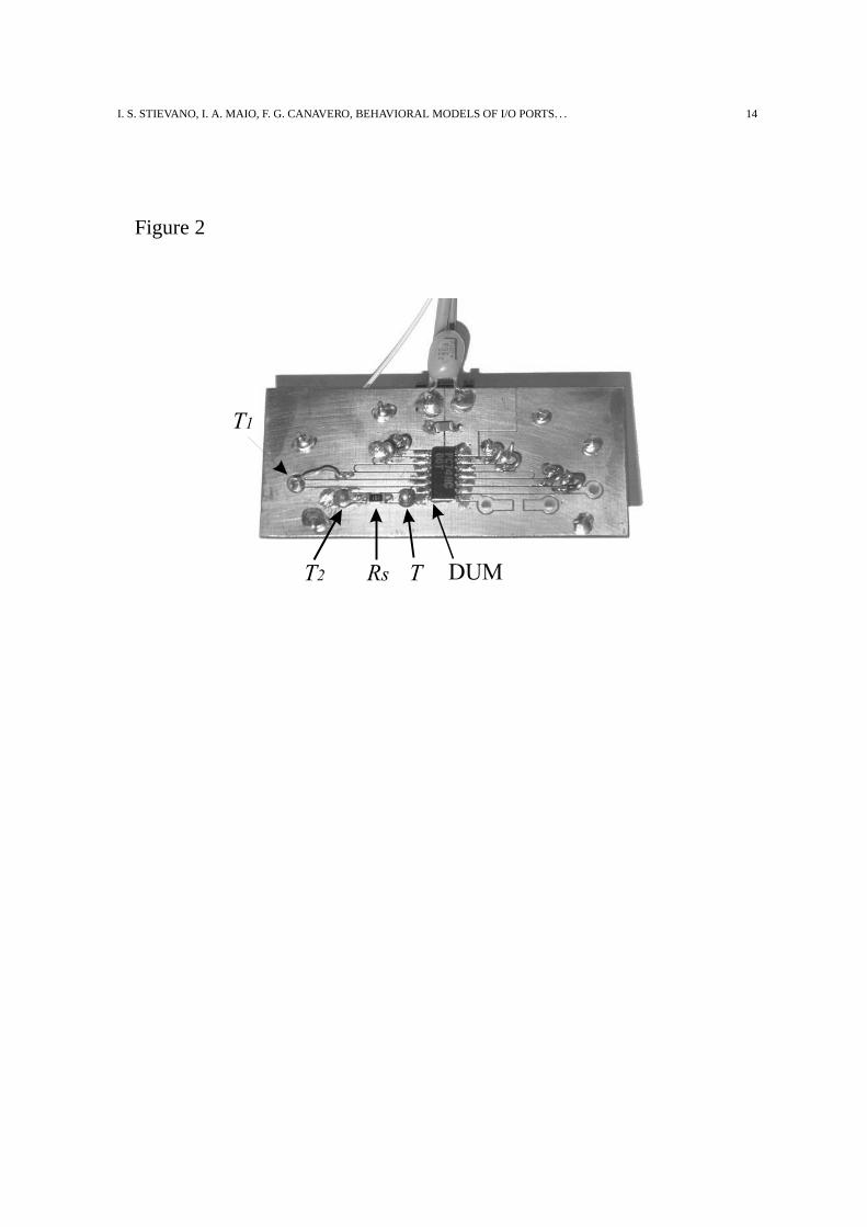
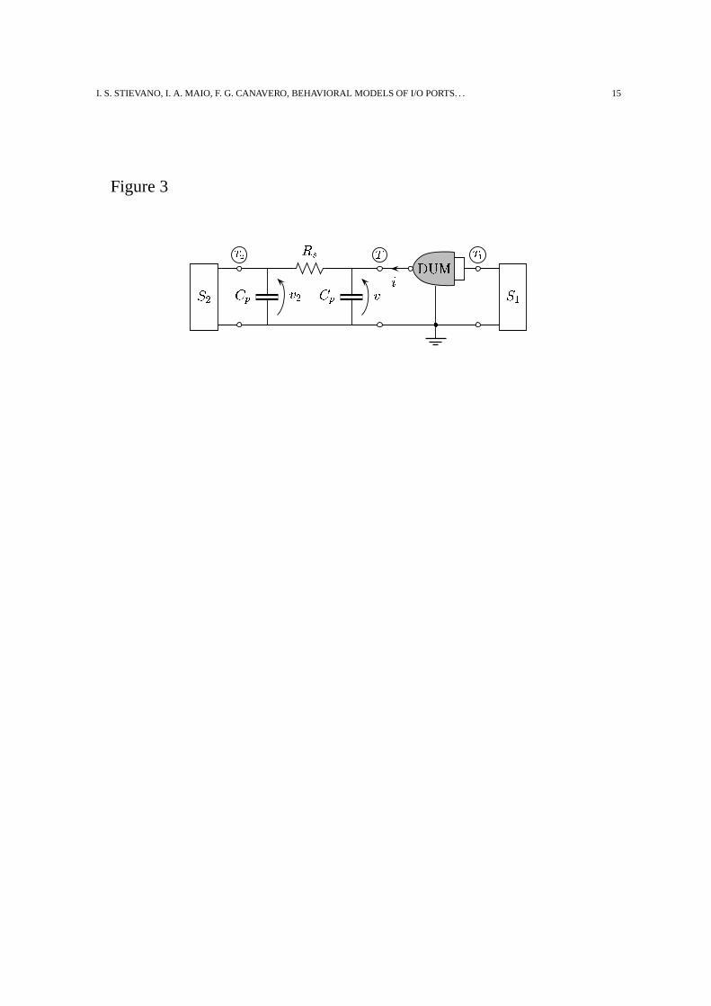
measured by means of the test fixture shown in Fig. 2. The equivalent circuit used to describe
the test fixture is shown in Fig. 3. In this equivalent, DUM represents the port being modeled,� �
the SMD resistor of Fig. 2, terminal�
is the pin of the port being modeled, and�
and� �
are the input and output terminals used to stimulate the circuit via sources � and � � ,respectively. Terminals
�and
���are connected to SMA connectors on the back of the board
of Fig. 2, that are used to inject the signals of source � � and to connect scope probes. The
scope probes detect the voltage waveforms�������
and� � �����
, and their presence is taken into
account by the shunt capacitors ��� .The identification signals described in subsection II-B are generated as follows. The port
responses�������
and�������
are obtained from the voltages recorded via the probes connected
to terminals�
and���
. The scope is a Tektronix TDS380 with � ( ( MHz bandwidth (�
Gs/s
sampling rate) and the probes are passive voltage probes P6114B (attenuation factor� (��
,
input resistance� (
M � , nominal value of the parasitic capacitance� � � pF). Current
�������is
indirectly obtained from the voltage drop on the SMD series resistor� �
(see Fig. 3) as
��������� ��� ��������� ��� � ������� � � � �����%$�� � �
In this application, the port switching times are sufficiently slow to allow the modeling of
I. S. STIEVANO, I. A. MAIO, F. G. CANAVERO, BEHAVIORAL MODELS OF I/O PORTS. . . 9
the SMD resistor by means of the ideal element� �
. However, an accurate characterization
of the SMD resistor by means of a network analyzer is needed for devices that exhibit faster
transition times.
The identification signals for the estimation of the RBF submodels�
and���
are generated
by using a multifunction waveform synthesizer connected as � � while the port being modeled
is set, via the source � , to either the High or the Low logic output state. The generator � � is
tuned to obtain a voltage waveform�������
with the required shape, i.e., a multilevel waveform
spanning the range of possible operating voltages. As an example, the identification signals
for submodel� �
obtained in this way are shown in Fig. 4. The waveform generator to excite
such signals is not a critical element. In this setup, the block � � producing the waveform
of Fig. 4 is a Rhode&Schwarz AFS multifunction generator connected to a suitable stub
element (i.e., a� ���
m long RG58 cable) and generating a�)(
MHz square wave with ade-
quate duty-cycle, offset and amplitude. In a setup for routine measurements, the waveform
generator could be provided by a dedicated circuit composed of discrete logic gates.
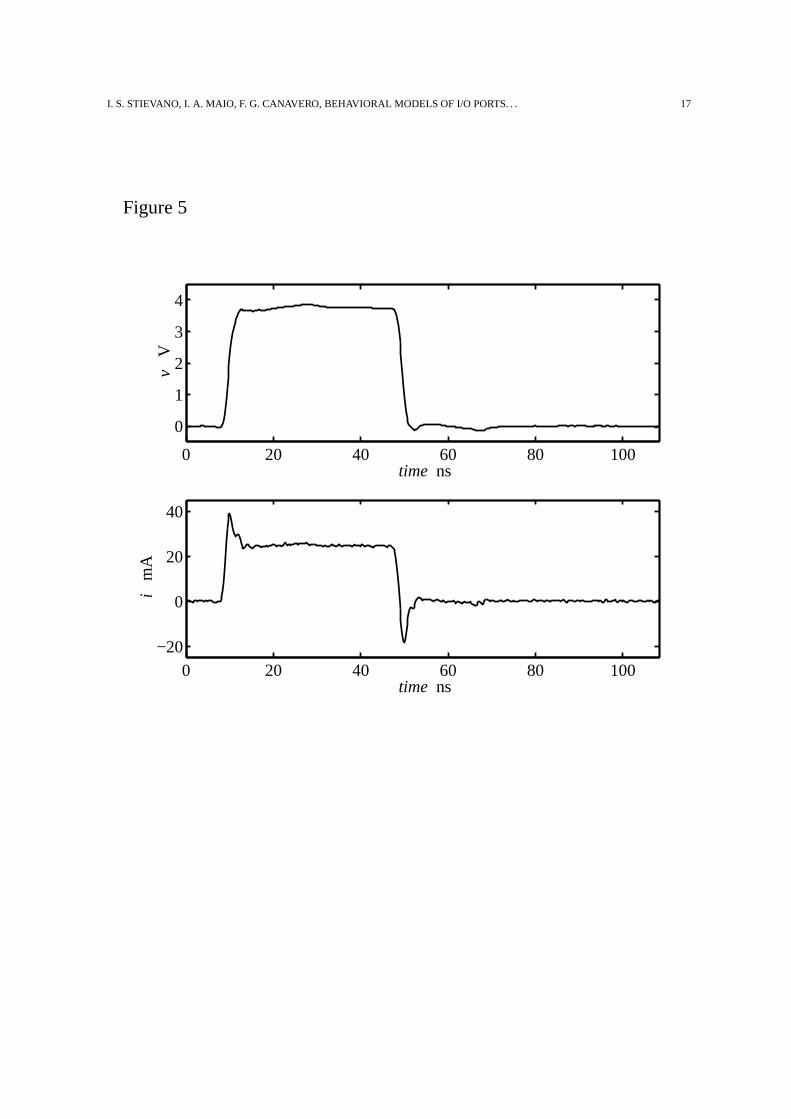
As a second step, the switching signals for the estimation of weight coefficients�
and���
, are obtained by replacing � � with a')( � coax resistor and with a
� ( � carbon resistor
connected to�����
as load (a) and load (b), respectively, and by driving (via � ) the port
to produce a high pulse. Figure 5 shows the identification signals for the above switching
experiment obtained while the port is connected to load (a).
It is worth noticing that an accurate characterization of loads and instruments (block � � in
the setup of Fig. 3) is not needed. Once � � is tuned to produce the wished shape of the port
voltage waveform�������
, the port current waveform�������
required for the estimation process
can be accurately measured by means of the voltage drop on the series resistor� �
, only.
The recorded identification signal are sampled by a sampling period� � �)( ( ��� (
� � ')(samples) and are processed by the estimation algorithm [6] to compute the submodel param-
eters� �
,� � � ���
. Then the weight coefficients are computed by using the switching signals
and the estimated submodels���
,� � � ���
as explained in subsection II-B. For this example,
model (2) is estimated in some tens seconds on a Pentium II PC and its submodels turn out

I. S. STIEVANO, I. A. MAIO, F. G. CANAVERO, BEHAVIORAL MODELS OF I/O PORTS. . . 10
to have dynamic order one (
"���
) and five basis functions each. The model is implemented
as a SPICE subcircuit by the procedure described in subsection II-C and is validated by pre-
dicting the responses of test circuits different from those involved in the generation of the
identification signals.
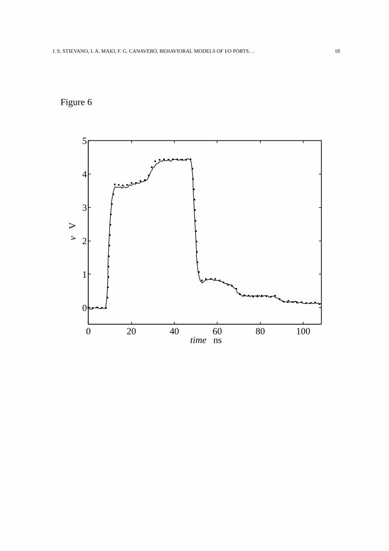
As an example, Fig. 6 shows the measured and the predicted responses of the modeled
port when it sends a pulse on the series connection of� �
and an open ended RG58 coaxial
cable. The accuracy of the model is clearly appreciable. In all tests carried out, the model
turns out to accurately reproduce both the static (steady-states) and the dynamic (transitions)
behavior of the actual port, leading to timing errors always less than the sampling period
used in the estimation process. In our tests, the timing error is defined as the maximum delay
between the reference and the model responses measured at one half of the signal swing.
These results show that the estimated model performs at a very good accuracy level, even if
the measurement of identification signals and the validation are based on a rather idealized
equivalent circuit of the test fixture. On the other hand, the structure of the model is simple
and has the numerical efficiency required for the simulation of realistic problems.
IV. CONCLUSIONS
The behavioral modeling of IC ports via black-box identification leads to simple and reli-
able models that can be easily included in a standard simulation environment. Identification
methods provide a rigorous framework to handle the problem and the proposed procedure
indeed enables final users to build their own IC models from actual measurements. In con-
clusion, the black-box approach could be a useful complement to the conventional circuit-
oriented ones for the development of models to be used in the simulation of EMC and SI
problems.

I. S. STIEVANO, I. A. MAIO, F. G. CANAVERO, BEHAVIORAL MODELS OF I/O PORTS. . . 11
REFERENCES
[1] ANSI/EIA-656-A, “I/O Buffer Information Specification (IBIS) version 3.2,” http://www.eigroup.org/IBIS, Electronic
Industries Alliance, Engineering Department, Arlington, VA, 1999.
[2] L. Ljung, System Identification: theory for the user. Prentice-Hall, 1987.
[3] I. S. Stievano, F. G. Canavero, I. A. Maio, “Parametric Macromodels of Digital I/O Ports”, IEEE Trans. Advanced
Packaging, Vol 25, No. 2, May 2002.
[4] J. Sjoberg et al., “Nonlinear Black-Box Modeling in System Identification: a Unified Overview,” Automatica, Vol. 31,
NO. 12, pp. 1691–1724, 1995.
[5] S. Chen, C. F. N. Cowan and P. M. Grant, “Ortogonal Least Squares Learning Algorithm for Radial Basis Function
Network,” IEEE Transactions on Neural Networks, Vol. 2, NO. 2, pp. 302–309, March 1991.
[6] K. Judd and A. Mees, “On selecting models for nonlinear time series,” Physica D, Vol. 82, pp. 426–444, 1995.
[7] M. Autin, M. Biey and M. Hasler, “Order of discrete time nonlinear systems determined from input/output signals,”
Proc. of ISCAS-92, pp. 296–299, May 1992.
[8] F. G. Canavero, I. A. Maio, I. S. Stievano, “Black-Box Models of Digital IC ports for EMC simulations,” in ����� � IEEE
International Zurich Symposium on Electromagnetic Compatibility, Zurich, CH, pp. 679–684, February 20–22, 2001.
[9] I. S. Stievano, F. G. Canavero, Z. Chen, G. Katopis, I. A. Maio, “High Performance RBF Models of Digital Drivers,”
in � � � IEEE Workshop on Signal Propagation on Interconnects, Venice, I, May 13–16, 2001.

I. S. STIEVANO, I. A. MAIO, F. G. CANAVERO, BEHAVIORAL MODELS OF I/O PORTS. . . 12
Figure captions:
Fig. 1 Generic multistage output buffer and its relevant electric variables.
Fig. 2 Test fixture for the experimental characterization of the output port of a HC7400 IC.
The DUM is the port being modeled,� �
is the SMD resistor and�
,�
and� �
are the
terminals shown in the equivalent circuit of Fig. 3.
Fig. 3 Equivalent circuit of the identification setup.� � � � ( ( � and �� ��� � � pF represents
the SMD resistor and the passive voltage probe, respectively. � and � � are the sources of
the identification signals (see text for more details).
Fig. 4 Measured switching identification signals�������
and�������
for the estimation of submodel���
.
Fig. 5 Measured identification signals for the estimation of weight coefficients�
and���
while the port is connected to load (a), i.e., the series connection of� � � � ( ( � and a
')( �coax resistor.
Fig. 6 Output voltage waveform of the port being modeled driving a series connection of a� ( ( � resistor and an open ended
� 'm long RG58 coaxial cable ( ��� � ')( � ). Solid line:
measured reference response; dotted line: response of the two-piece RBF model.

I. S. STIEVANO, I. A. MAIO, F. G. CANAVERO, BEHAVIORAL MODELS OF I/O PORTS. . . 13
Figure 1
������ �
�
�����
�� � �
� �
I. S. STIEVANO, I. A. MAIO, F. G. CANAVERO, BEHAVIORAL MODELS OF I/O PORTS. . . 14
Figure 2
DUMT2
T1
TRs
I. S. STIEVANO, I. A. MAIO, F. G. CANAVERO, BEHAVIORAL MODELS OF I/O PORTS. . . 15
Figure 3
�
������
���
� � ��
��� � ���
� � ���

I. S. STIEVANO, I. A. MAIO, F. G. CANAVERO, BEHAVIORAL MODELS OF I/O PORTS. . . 16
Figure 4
0 50 100 150 200 250
0
2
4
6
time ns
v
V
0 50 100 150 200 250−60
−40
−20
0
20
time ns
i m
A
I. S. STIEVANO, I. A. MAIO, F. G. CANAVERO, BEHAVIORAL MODELS OF I/O PORTS. . . 17
Figure 5
0 20 40 60 80 100
0
1
2
3
4
time ns
v
V
0 20 40 60 80 100−20
0
20
40
time ns
i m
A
I. S. STIEVANO, I. A. MAIO, F. G. CANAVERO, BEHAVIORAL MODELS OF I/O PORTS. . . 18
Figure 6
0 20 40 60 80 100
0
1
2
3
4
5
v
V
time ns