Nanoscale interface engineering in ZnO twin nanorods for proposed phonon tunnel devices
9
This is an Accepted Manuscript, which has been through the Royal Society of Chemistry peer review process and has been accepted for publication. Accepted Manuscripts are published online shortly after acceptance, before technical editing, formatting and proof reading. Using this free service, authors can make their results available to the community, in citable form, before we publish the edited article. We will replace this Accepted Manuscript with the edited and formatted Advance Article as soon as it is available. You can find more information about Accepted Manuscripts in the Information for Authors. Please note that technical editing may introduce minor changes to the text and/or graphics, which may alter content. The journal’s standard Terms & Conditions and the Ethical guidelines still apply. In no event shall the Royal Society of Chemistry be held responsible for any errors or omissions in this Accepted Manuscript or any consequences arising from the use of any information it contains. Accepted Manuscript www.rsc.org/pccp PCCP View Article Online View Journal This article can be cited before page numbers have been issued, to do this please use: A. Singh, K. Senapati, B. Satpati, M. Kumar and P. K. Sahoo, Phys. Chem. Chem. Phys., 2014, DOI:
Transcript of Nanoscale interface engineering in ZnO twin nanorods for proposed phonon tunnel devices

This is an Accepted Manuscript, which has been through the Royal Society of Chemistry peer review process and has been accepted for publication.
Accepted Manuscripts are published online shortly after acceptance, before technical editing, formatting and proof reading. Using this free service, authors can make their results available to the community, in citable form, before we publish the edited article. We will replace this Accepted Manuscript with the edited and formatted Advance Article as soon as it is available.
You can find more information about Accepted Manuscripts in the Information for Authors.
Please note that technical editing may introduce minor changes to the text and/or graphics, which may alter content. The journal’s standard Terms & Conditions and the Ethical guidelines still apply. In no event shall the Royal Society of Chemistry be held responsible for any errors or omissions in this Accepted Manuscript or any consequences arising from the use of any information it contains.
Accepted Manuscript
www.rsc.org/pccp
PCCP
View Article OnlineView Journal
This article can be cited before page numbers have been issued, to do this please use: A. Singh, K.
Senapati, B. Satpati, M. Kumar and P. K. Sahoo, Phys. Chem. Chem. Phys., 2014, DOI:
Journal Name
Cite this: DOI: 10.1039/c0xx00000x
www.rsc.org/xxxxxx
Dynamic Article Links ►
ARTICLE TYPE
This journal is © The Royal Society of Chemistry [year] [journal], [year], [vol], 00–00 | 1
Nanoscale interface engineering in ZnO twin nanorods
for proposed phonon tunnel devices
Avanendra Singh1, Kartik Senapati
1*, Biswarup Satpati
2, Mohit Kumar
3, and
Pratap K. Sahoo1*
5
Zinc oxide twin nanorods, with two identical crystalline sections connected by an amorphous layer, were
reproducibly grown by a simple one-step hydrothermal technique. The thickness of the amorphous layer
between the crystalline segments was tunable with growth parameters, as confirmed by high resolution
transmission electron microscopy. The photoluminescence spectra of these twin nanorods exhibit strong near
band edge emission in the UV range, with convoluted phonon sidebands. De-convolution analysis of these 10
spectra showed that the amorphous inter layers act as effective phonon barrier beyond certain thickness.
Such oriented grown individual crystalline-amorphous-crystalline structures may be a suitable test system
for fundamental studies of phonon tunneling in nanostructure. While physical vapor deposition techniques
are seriously constrained in realizing crystalline-amorphous-crystalline structures, our results show the
viability of engineering embedded interfaces by chemical routes. 15
Introduction:
Fundamental understanding of the phonon transport process in
nanostructures is rapidly gaining importance1-3 because phonons 20
can both be detrimental and beneficial to the functionality of
nanoscale devices. For example, optoelectronic applications of
widely studied ZnO based devices4-8 invariably excite optical
phonon modes in the system due to the built-in polarity in the
crystal structure9. From the perspective of electronic transport in 25
these devices, minimization of electron-phonon scattering is
desirable, whereas, efficient phonon transport is essential from
the perspective of waste heat management in the nano-structures
for large scale integration. Therefore, optimization of phonon
transport is an important design consideration for the present day 30
nanoscale devices. In this context, understanding phonon
tunneling process assumes analogous importance as
understanding electron tunneling in nano-junctions. There are,
however, little experimental efforts towards a direct study of
phonon tunneling in mesoscopic structures. Recently, Cole et 35
al.10 analyzed the clamping loss in micro-mechanical resonators
using a phonon tunneling approached developed by Wilson-
Rae11. However, a junction based phonon-tunneling
measurement, truly analogous to metal-insulator-metal type
electron tunnel junctions, is still lacking in the literature. The 40
insulating barrier between the metallic electrodes, in an electron
tunnel junction, forbids classical electron transport across the
junction. However, when the insulating barrier is made
sufficiently thin, quantum mechanics allows for a finite
probability of electron tunneling across the junction. In the same 45
spirit, a phonon junction should ideally comprise of a thin
amorphous layer sandwiched between two crystalline segments
grown with the same crystal orientation. Since the amorphous
layer can damp out certain phonon modes which freely propagate
through the crystalline segments, such crystalline-amorphous-50
crystalline (CAC) structures can facilitate a true phonon tunneling
measurement. A major obstacle for such measurements is the
difficulty in fabricating CAC structures with tunable barrier
thickness. Typically, electron tunnel junctions are prepared by a
combination of lithographic techniques and in-situ physical vapor 55
deposition of metals and insulator layers. For an equivalent
phonon tunnel junction, one ideally requires a CAC structure
where both crystalline segments have the same lattice orientation.
In the standard physical vapor deposition techniques, such as
sputtering, evaporation, and pulsed laser deposition etc., it is 60
almost impossible to grow an oriented structure on top of an
amorphous layer. Here we overcome this difficulty by employing
Page 1 of 8 Physical Chemistry Chemical Physics
Phy
sica
lChe
mis
try
Che
mic
alP
hysi
csA
ccep
ted
Man
uscr
ipt
Publ
ishe
d on
24
Dec
embe
r 20
14. D
ownl
oade
d by
Nat
iona
l Ins
titut
e of
Sci
ence
Edu
catio
n &
Res
earc
h on
28/
12/2
014
06:1
2:24
. View Article Online
DOI: 10.1039/C4CP05369A
2 | Journal Name, [year], [vol], 00–00 This journal is © The Royal Society of Chemistry [year]
the well established aqueous solution based chemical growth
techniques of oriented semiconducting nanorods. ZnO is ideally
suited for this purpose due to the well established growth
techniques and due to the polar nature of ZnO crystal, which
excites optical phonon modes. 5
Due to the large exciton binding energy and wide band gap, ZnO
has been extensively studied in the literature12,13 as potential
optoelectronics material5-8, energy material14-15, and sensing
applications16. Typically free standing aggregates of ZnO
nanostructures are prepared for these studies, using vapor 10
phase17,18 or aqueous solution based19-21 growth methods. Among
the standard processing routes of ZnO, hydrothermal method22-24
is a particularly simple, low temperature ( 90 0C) route which
provides multiple control parameters such as, temperature,
pressure, molarity of the aqueous solution, and choice of 15
precursors. A variety of multiply connected low dimensional ZnO
structures have also been reported in the literature25-30 prepared
by the hydrothermal route27-30. Recently, the growth of twin
Nanosphere and nanorods have generated considerable interest
due to their unique anisotropic light emission31-33. In this paper 20
we report controllable growth of CAC type ZnO nanorods using
the simple hydrothermal route. A closer inspection of the
segmented nanorods by transmission electron microscopy
confirmed two identical segments of single crystalline ZnO
connected through a well defined amorphous interface. Since the 25
width of these amorphous barriers was controllable via growth
parameters, such twin-nanorod junctions (TNRJs) are suitable
candidates for a systematic study of phonon tunneling process.
We discuss the suitability of these TNRJs for phonon tunneling
experiments based on the analysis of photo-luminescent (PL) 30
spectra.
Experimental details
P-type Si (100) substrates were used in all case. Prior to nanowire
growth, all substrates were coated with a thin layer of ZnO (~30
nm) using pulsed DC magnetron sputtering in a vacuum chamber 35
with a base pressure of 2×10⁻⁷ mbar. The sole purpose of the ZnO
coating was to ensure a fixed surface chemistry for all samples.
Twin ZnO nanorods were synthesized by hydrothermal process
using GR grade Zinc nitrate hexahydrate (Zn(NO3)2 . 6H2O,
99%) and hexamethylenetetramine (HMTA, (CH2)6N4, 99.99%), 40
from Sigma-Aldrich. An aqueous solution mixture of both Zinc
nitrate and HMTA was prepared in 1:1 ratio with three different
molar concentration of 0.01, 0.05 and 0.1 M by continuously
stirring on a stir plate for 30 minutes. A screw capped laboratory
30 ml Borosil bottle was filled with the mixture placing the ZnO 45
coated substrates under the cap with the surface facing down in to
the reaction precursor. The nanorod growth was initiated by
placing the bottle in a water bath on a regular laboratory oven.
Samples were prepared at reaction temperatures ranging from 60
0C to 90 0C. In order to vary the growth duration, keeping all 50
other parameters same, we placed separate identical screw capped
bottles simultaneously in the water bath. The temperature of the
reaction mixture was raised to the desired reaction temperature in
30 minutes in all cases, starting from room temperature of ~ 30
0C. Bottles were removed sequentially from the oven after the 55
desired growth durations of 1, 3, 6, 9, and 12 hours. After the
specific growth time at the desired temperature, the bottles were
cooled down naturally to room temperature. Subsequently, the
samples were taken out of the bottle and immediately rinsed
thoroughly with de-ionized water to remove residual salt. 60
The nanorods were inspected using field emission scanning
electron microscopy (FESEM). Preliminary composition check of
the ZnO nanorods was done by Oxford made X-ray energy
dispersive spectrometer (EDS) attached to the FESEM system.
At least five different areas on each substrate were imaged to 65
measure the nanorod density and to obtain the statistics on length
and width values. High resolution transmission electron
microscope (HRTEM), selected area electron diffraction (SAED),
electron energy loss spectroscopy (EELS), and X-ray diffraction
techniques were used to check crystal structure and growth 70
orientation. The room temperature photoluminescence (PL)
spectra were recorded using a FS920 Edinburgh unit using 325
nm, 15mW He-Cd laser as excitation source. The PL signal was
collected using a single photon counting plug-in PC card with a
resolution of 0.01 nm, and amplified by Hamamatsu R955 75
photomultiplier in a Peltier cooled housing. In all cases the twin
nano wires were found uniformly spread over the entire substrate.
Several PL scans from different parts of the same sample showed
the same spectral features with only minor intensity variations.
Results and discussion 80
Page 2 of 8Physical Chemistry Chemical Physics
Phy
sica
lChe
mis
try
Che
mic
alP
hysi
csA
ccep
ted
Man
uscr
ipt
Publ
ishe
d on
24
Dec
embe
r 20
14. D
ownl
oade
d by
Nat
iona
l Ins
titut
e of
Sci
ence
Edu
catio
n &
Res
earc
h on
28/
12/2
014
06:1
2:24
. View Article Online
DOI: 10.1039/C4CP05369A
This journal is © The Royal Society of Chemistry [year] Journal Name, [year], [vol], 00–00 | 3
In a typical hydrothermal process, the precursor solution is
allowed to react at a fixed reaction temperature (TR), with the
substrate immersed in the aqueous solution22-24. The resulting
nanorods grow as uniform crystalline structures on the substrate.
A rather unexplored aspect of the hydrothermal process is the 5
ability to form amorphous clusters of ZnO at temperatures below
TR, due to the lack of sufficient thermal energy for crystallization.
For realizing ZnO nanorods in the CAC architecture, the
amorphous region is desired at the middle of individual
crystalline rods. For this purpose, unlike the standard practice, the 10
substrates immersed in precursor solution were allowed to attain
the final reaction temperature gradually from room temperature.
During the initial stages of temperature ramping (below TR)
amorphous ZnO clusters grow at a slow rate until temperature
reaches a minimum value of TR. The minimum reaction 15
temperature was found to be ~60 0C, for our experimental set-up.
As the temperature reaches the minimum value of TR, ZnO
crystals start nucleating symmetrically from both sides of these
amorphous clusters, ultimately providing the TNRJs in a CAC
structure. The temperature ramp rate (Rr), therefore, determines 20
the width of the amorphous layer in the TNRJs.
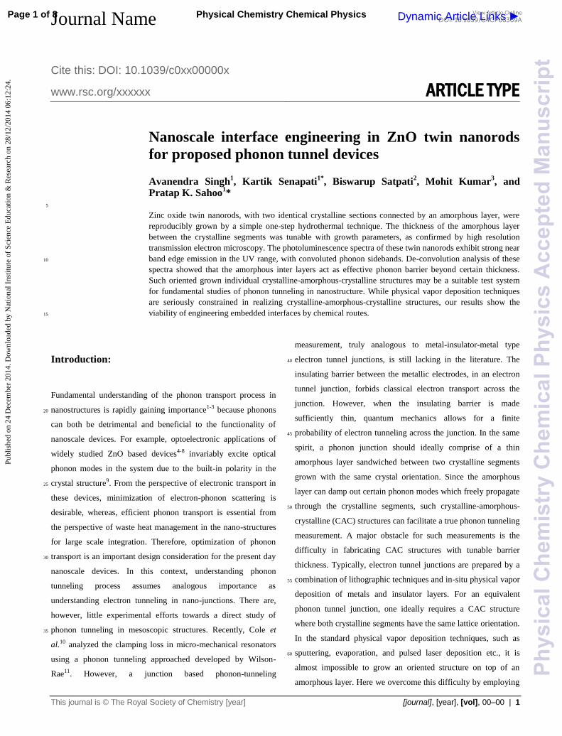
Fig. 1 (a), (b), and (c) show the scanning electron micrographs of ZnO
nanorods prepared by this method at TR = 60 0C (d) sample image of a
single nanorod grown at a reaction temperature of 90 0C. The selected 25
area diffraction patterns from both sides of the nanorods are shown in the
panels (e) and (f).
Fig. 1 Panels (a), (b), and (c) show the scanning electron
micrograph of twin nanorods prepared at a final reaction
temperature of 60 0C, 80 0C, and 90 0C, respectively. Panel (d) 30
shows a transmission electron
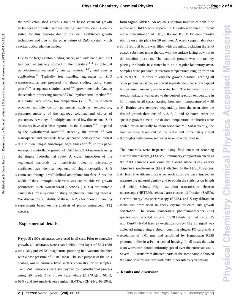
Fig. 2 Glancing angle (20) X-ray diffraction pattern of ZnO nanorods
grown on Si substrates (*) at a reaction temperature of 800C. Only (00l)
peaks are observed, owing to the highly oriented crystalline ZnO
nanorods. 35
`a'), 80 0C (sample `b') and 90 0C (sample `c'), respectively. In all
cases the final reaction temperature was reached in 30 minutes,
with effective ramp rates of ~1 0C/min, ~1.7 0C/min, and ~2
0C/min for samples a, b, and c, respectively. In all cases,
hexagonal nanorods were obtained with a clear groove at mid 40
length. Energy dispersive X-ray (EDX) analysis of the central
grooved region did not show any signature of contamination,
confirming continuous growth of ZnO crystals from amorphous
ZnO. The dimensions of the nanorods were found to scale with
the molar concentration of the precursor, TR, and the reaction 45
time, as expected. ZnO bipod structures have been reported
earlier by Jang et al.24, where acetate-intercalated zinc hydroxide
double salt (Zn-HDS) was used as bi-directional nucleation seed
for ZnO. This method, however, does not allow any control over
the thickness of the interface between the two sides of the bipods, 50
which is an essential feature for junction architecture. Figure 1(d)
shows the transmission electron micrograph (TEM) of a nanorod
prepared at 90 0C. Selected area electron diffraction (SAED)
patterns on both sides of the central groove, shown in panels (e)
and (f) in Fig. 1, confirm the crystalline nature of the [0001] 55
grown nanorods. Grazing incidence X-ray diffraction
measurements indicated (0001) oriented growth of the nanorods,
as shown in Figure 2. Figure 3 (panels (a), (b), (c) , (e), and (f))
shows the scanning transmission electron microscopy (STEM)-
energy dispersive x-ray (EDX) elemental map of a nanorod 60
across the central groove. The line scan in panel (d) of Fig.3
30 40 50 60 70 80
*
* (004
)
Inte
nsi
ty (
arb
. U
nit)
2 (degree)
(002
)
*
Reaction Temperature = 80 oC
Page 3 of 8 Physical Chemistry Chemical Physics
Phy
sica
lChe
mis
try
Che
mic
alP
hysi
csA
ccep
ted
Man
uscr
ipt
Publ
ishe
d on
24
Dec
embe
r 20
14. D
ownl
oade
d by
Nat
iona
l Ins
titut
e of
Sci
ence
Edu
catio
n &
Res
earc
h on
28/
12/2
014
06:1
2:24
. View Article Online
DOI: 10.1039/C4CP05369A
4 | Journal Name, [year], [vol], 00–00 This journal is © The Royal Society of Chemistry [year]
Fig. 3 Panel (a) shows the scanning transmission electron microscope
image of a typical twin ZnO nanorod. Panel (b) shows the HAADF-
STEM image for compositional sensitivity. Panels (c), (f) and (e) show
elemental mapping for Zn, O and the composite image, respectively.
Panel (f) shows the line scan across the junction. Panel (g) shows the 5
STEM-EDX spectrum of the selected region in panel (a), confirming the
presence of only Zn and O in the junction region. The Cu signal in this
spectrum is from the Copper grid used in TEM imaging.
shows the Zn-L and O-K signals across the junction region. No
signature of impurities was found in the amorphous region or 10
along the body of the nanorod within the detection limit of
STEM-EDX (0.1 at%). The EDX spectrum from the selected area
of panel (a) is shown in panel (g) of Fig. 3. Apart from the Cu
signal from the TEM grid, only Zn and O signals were detected
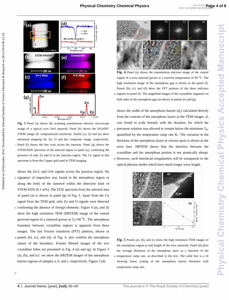
confirming the absence of foreign elements. Figure 4 (a), and (f) 15
show the high resolution TEM (HRTEM) image of the central
grooved region of a nanorod grown at TR=60 0C. The amorphous
boundary between crystalline regions is apparent from these
images. The fast Fourier transform (FFT) patterns, shown in
panels (b), (c), and (d), of Fig. 4, also confirm the amorphous 20
nature of the boundary. Fourier filtered images of the two
crystalline lobes are presented in Fig. 4 (e) and (g). In Figure 5
(a), (b), and (c) we show the HRTEM images of the amorphous
barrier regions of samples a, b, and c, respectively. Figure 5 (d)
25
Fig. 4 Panel (a) shows the transmission electron image of the central
region of a twin nanorod grown at a reaction temperature of 60 0C. The
high resolution image of the amorphous gap is shown in the panel (f).
Panels (b), (c) and (d) show the FFT patterns of the three indicates
regions in panel (f). The magnified images of the crystalline segments on 30
both sides of the amorphous gap are shown in panels (e) and (g).
shows the width of the amorphous barrier (da) calculated directly
from the contrast of the amorphous layers in the TEM images. da
was found to scale linearly with the duration, for which the
precursor solution was allowed to remain below the minimum TR, 35
quantified by the temperature ramp rate Rr. The variation in the
thickness of the amorphous layers at various spots is shown as the
error bars. HRTEM shows that the interface between the
crystalline and the amorphous portion is not atomically abrupt.
However, such interfacial irregularities will be transparent to the 40
optical phonon modes which have much longer wave length.
Fig. 5 Panels (a), (b), and (c) show the high resolution TEM images of
the amorphous region at mid length of the twin nanorods. Panel (d) plots
the average thickness of the amorphous layer as a function of the
temperature ramp rate, as described in the text. The solid line is a fit 45
showing linear scaling of the amorphous barrier thickness with
temperature ramp rate.
Page 4 of 8Physical Chemistry Chemical Physics
Phy
sica
lChe
mis
try
Che
mic
alP
hysi
csA
ccep
ted
Man
uscr
ipt
Publ
ishe
d on
24
Dec
embe
r 20
14. D
ownl
oade
d by
Nat
iona
l Ins
titut
e of
Sci
ence
Edu
catio
n &
Res
earc
h on
28/
12/2
014
06:1
2:24
. View Article Online
DOI: 10.1039/C4CP05369A
This journal is © The Royal Society of Chemistry [year] Journal Name, [year], [vol], 00–00 | 5
Having established the formation of crystalline-amorphous-
crystalline type TNRJs with controllable amorphous barrier we
now discuss the suitability of these nanorods as effective phonon
tunneling devices in which the barrier has low phonon
transparency. For this purpose, we have utilized the characteristic 5
phonon sidebands of free-exciton (FX) emission peaks, typically
observed in PL spectra of wurtzite ZnO34-36. Such sideband
emissions occur when free-excitons decay via emission of optical
phonons. ZnO, being a polar semiconductor, experiences strong
Frohlich interaction leading to frequent decay of free excitons via 10
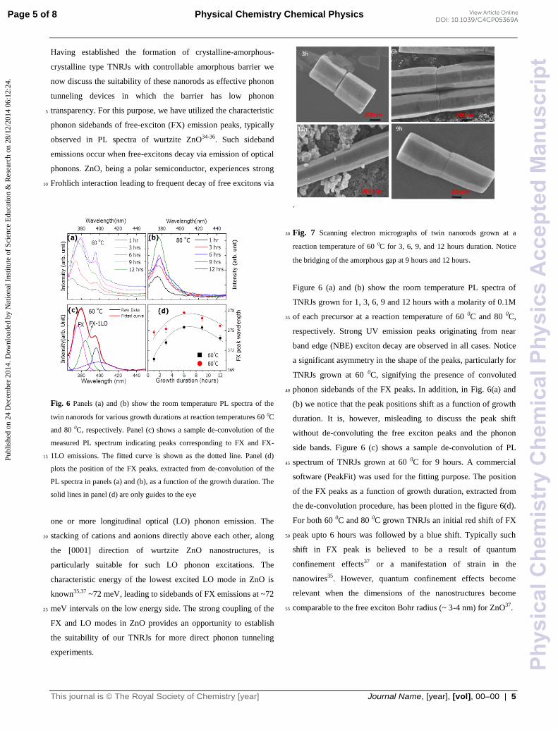
Fig. 6 Panels (a) and (b) show the room temperature PL spectra of the
twin nanorods for various growth durations at reaction temperatures 60 0C
and 80 0C, respectively. Panel (c) shows a sample de-convolution of the
measured PL spectrum indicating peaks corresponding to FX and FX-
1LO emissions. The fitted curve is shown as the dotted line. Panel (d) 15
plots the position of the FX peaks, extracted from de-convolution of the
PL spectra in panels (a) and (b), as a function of the growth duration. The
solid lines in panel (d) are only guides to the eye
one or more longitudinal optical (LO) phonon emission. The
stacking of cations and aonions directly above each other, along 20
the [0001] direction of wurtzite ZnO nanostructures, is
particularly suitable for such LO phonon excitations. The
characteristic energy of the lowest excited LO mode in ZnO is
known35,37 ~72 meV, leading to sidebands of FX emissions at ~72
meV intervals on the low energy side. The strong coupling of the 25
FX and LO modes in ZnO provides an opportunity to establish
the suitability of our TNRJs for more direct phonon tunneling
experiments.
.
Fig. 7 Scanning electron micrographs of twin nanorods grown at a 30
reaction temperature of 60 0C for 3, 6, 9, and 12 hours duration. Notice
the bridging of the amorphous gap at 9 hours and 12 hours.
Figure 6 (a) and (b) show the room temperature PL spectra of
TNRJs grown for 1, 3, 6, 9 and 12 hours with a molarity of 0.1M
of each precursor at a reaction temperature of 60 0C and 80 0C, 35
respectively. Strong UV emission peaks originating from near
band edge (NBE) exciton decay are observed in all cases. Notice
a significant asymmetry in the shape of the peaks, particularly for
TNRJs grown at 60 0C, signifying the presence of convoluted
phonon sidebands of the FX peaks. In addition, in Fig. 6(a) and 40
(b) we notice that the peak positions shift as a function of growth
duration. It is, however, misleading to discuss the peak shift
without de-convoluting the free exciton peaks and the phonon
side bands. Figure 6 (c) shows a sample de-convolution of PL
spectrum of TNRJs grown at 60 0C for 9 hours. A commercial 45
software (PeakFit) was used for the fitting purpose. The position
of the FX peaks as a function of growth duration, extracted from
the de-convolution procedure, has been plotted in the figure 6(d).
For both 60 0C and 80 0C grown TNRJs an initial red shift of FX
peak upto 6 hours was followed by a blue shift. Typically such 50
shift in FX peak is believed to be a result of quantum
confinement effects37 or a manifestation of strain in the
nanowires35. However, quantum confinement effects become
relevant when the dimensions of the nanostructures become
comparable to the free exciton Bohr radius (~ 3-4 nm) for ZnO37. 55
Page 5 of 8 Physical Chemistry Chemical Physics
Phy
sica
lChe
mis
try
Che
mic
alP
hysi
csA
ccep
ted
Man
uscr
ipt
Publ
ishe
d on
24
Dec
embe
r 20
14. D
ownl
oade
d by
Nat
iona
l Ins
titut
e of
Sci
ence
Edu
catio
n &
Res
earc
h on
28/
12/2
014
06:1
2:24
. View Article Online
DOI: 10.1039/C4CP05369A
6 | Journal Name, [year], [vol], 00–00 This journal is © The Royal Society of Chemistry [year]
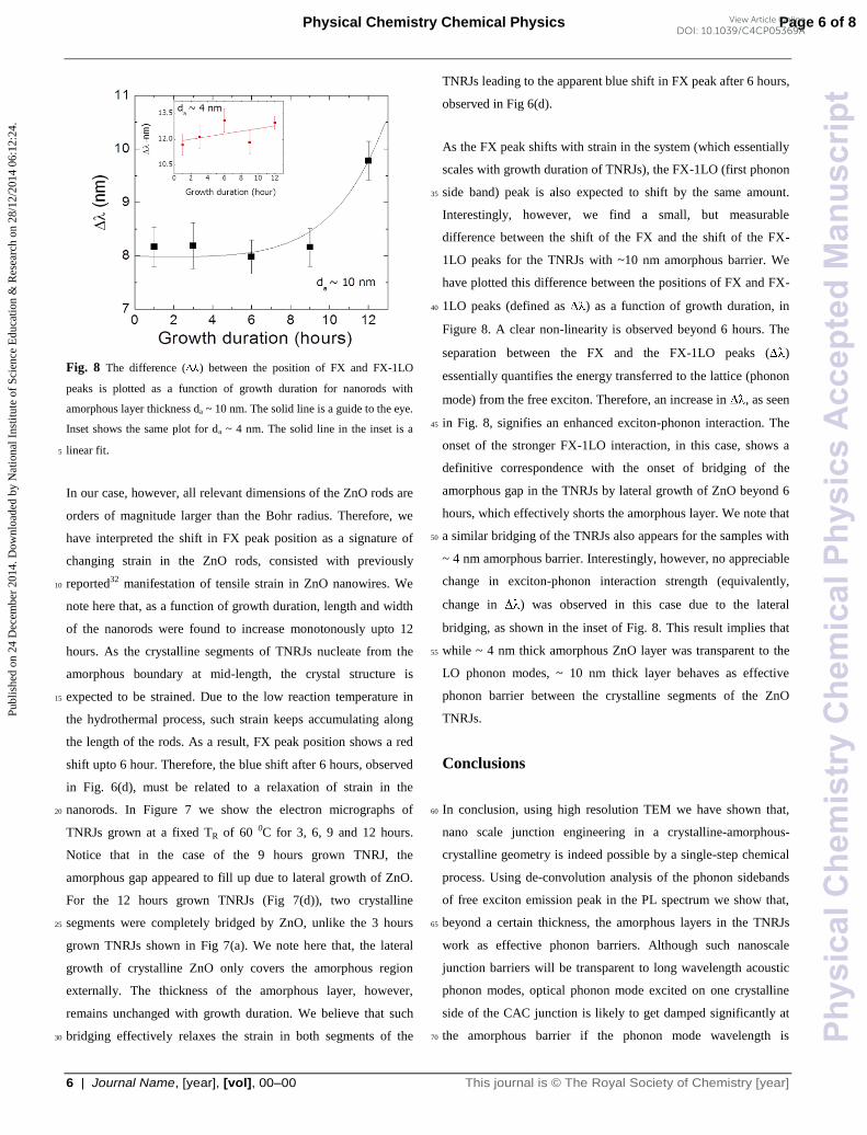
Fig. 8 The difference ( ) between the position of FX and FX-1LO
peaks is plotted as a function of growth duration for nanorods with
amorphous layer thickness da ~ 10 nm. The solid line is a guide to the eye.
Inset shows the same plot for da ~ 4 nm. The solid line in the inset is a
linear fit. 5
In our case, however, all relevant dimensions of the ZnO rods are
orders of magnitude larger than the Bohr radius. Therefore, we
have interpreted the shift in FX peak position as a signature of
changing strain in the ZnO rods, consisted with previously
reported32 manifestation of tensile strain in ZnO nanowires. We 10
note here that, as a function of growth duration, length and width
of the nanorods were found to increase monotonously upto 12
hours. As the crystalline segments of TNRJs nucleate from the
amorphous boundary at mid-length, the crystal structure is
expected to be strained. Due to the low reaction temperature in 15
the hydrothermal process, such strain keeps accumulating along
the length of the rods. As a result, FX peak position shows a red
shift upto 6 hour. Therefore, the blue shift after 6 hours, observed
in Fig. 6(d), must be related to a relaxation of strain in the
nanorods. In Figure 7 we show the electron micrographs of 20
TNRJs grown at a fixed TR of 60 0C for 3, 6, 9 and 12 hours.
Notice that in the case of the 9 hours grown TNRJ, the
amorphous gap appeared to fill up due to lateral growth of ZnO.
For the 12 hours grown TNRJs (Fig 7(d)), two crystalline
segments were completely bridged by ZnO, unlike the 3 hours 25
grown TNRJs shown in Fig 7(a). We note here that, the lateral
growth of crystalline ZnO only covers the amorphous region
externally. The thickness of the amorphous layer, however,
remains unchanged with growth duration. We believe that such
bridging effectively relaxes the strain in both segments of the 30
TNRJs leading to the apparent blue shift in FX peak after 6 hours,
observed in Fig 6(d).
As the FX peak shifts with strain in the system (which essentially
scales with growth duration of TNRJs), the FX-1LO (first phonon
side band) peak is also expected to shift by the same amount. 35
Interestingly, however, we find a small, but measurable
difference between the shift of the FX and the shift of the FX-
1LO peaks for the TNRJs with ~10 nm amorphous barrier. We
have plotted this difference between the positions of FX and FX-
1LO peaks (defined as ) as a function of growth duration, in 40
Figure 8. A clear non-linearity is observed beyond 6 hours. The
separation between the FX and the FX-1LO peaks ( )
essentially quantifies the energy transferred to the lattice (phonon
mode) from the free exciton. Therefore, an increase in , as seen
in Fig. 8, signifies an enhanced exciton-phonon interaction. The 45
onset of the stronger FX-1LO interaction, in this case, shows a
definitive correspondence with the onset of bridging of the
amorphous gap in the TNRJs by lateral growth of ZnO beyond 6
hours, which effectively shorts the amorphous layer. We note that
a similar bridging of the TNRJs also appears for the samples with 50
~ 4 nm amorphous barrier. Interestingly, however, no appreciable
change in exciton-phonon interaction strength (equivalently,
change in ) was observed in this case due to the lateral
bridging, as shown in the inset of Fig. 8. This result implies that
while ~ 4 nm thick amorphous ZnO layer was transparent to the 55
LO phonon modes, ~ 10 nm thick layer behaves as effective
phonon barrier between the crystalline segments of the ZnO
TNRJs.
Conclusions
In conclusion, using high resolution TEM we have shown that, 60
nano scale junction engineering in a crystalline-amorphous-
crystalline geometry is indeed possible by a single-step chemical
process. Using de-convolution analysis of the phonon sidebands
of free exciton emission peak in the PL spectrum we show that,
beyond a certain thickness, the amorphous layers in the TNRJs 65
work as effective phonon barriers. Although such nanoscale
junction barriers will be transparent to long wavelength acoustic
phonon modes, optical phonon mode excited on one crystalline
side of the CAC junction is likely to get damped significantly at
the amorphous barrier if the phonon mode wavelength is 70
Page 6 of 8Physical Chemistry Chemical Physics
Phy
sica
lChe
mis
try
Che
mic
alP
hysi
csA
ccep
ted
Man
uscr
ipt
Publ
ishe
d on
24
Dec
embe
r 20
14. D
ownl
oade
d by
Nat
iona
l Ins
titut
e of
Sci
ence
Edu
catio
n &
Res
earc
h on
28/
12/2
014
06:1
2:24
. View Article Online
DOI: 10.1039/C4CP05369A
This journal is © The Royal Society of Chemistry [year] Journal Name, [year], [vol], 00–00 | 7
comparable to the thickness of the barrier. Measuring the
transmitted modal intensity of phonons on one crystalline side of
the barrier by exciting phonon modes on the other crystalline
side, using micro-Raman and atomic force microscopy based
techniques, would provide a direct measure of the phonon 5
tunneling co-efficient.
Acknowledgments
AS, KS, and PKS acknowledge the funding from National
Institute of Science Education and Research, India. KS and PKS
acknowledge the scientific discussion and technical help from 10
Prof. T. Som and Dr. S. Prusty.
Notes and References
1School of Physical Sciences, National Institute of Science Education and
Research (NISER) Bhubaneswar, Odisha, India-751005,0674-2304042, 2304028, E-mail: [email protected], [email protected], 15
2Surface physics & Materials Science Division, Saha Institute of Nuclear
Physics,1/AF Bidhannagar, Kolkata, India-700064 E-mail:
3Institute of Physics, Sachivalaya Marg, Bhubaneswar, Odisha, India-20
751005 E-mail: [email protected]
*Corresponding authors: [email protected], [email protected]
1. Z. T. Tian,B. E. White, Jr.,and Y. Sun Appl. Phys. Lett. 2010, 96,
263113.
2. N. Yang; X. Xu; G. Zhang; B.,Li; AIP Advances 2012, 2, 041410. 25
3. B. Li; J. Wang, Phys. Rev. Lett. 2003, 91, 044301.
4. A. B. Djurišić; A. M. C. Ng; X. Y. Chen, Prog. Quantum Electron.
2010, 34, 191-259.
5. M. Law; L. E. Greene; J. C. Johnson; R. Saykally; P. Yang, Nat.
Mater. 2005, 4, 455-459. 30
6. H. Kind; H. Yan; B. Messer; M. Law; P. Yang; Adv. Mater. 2002,
14, 158-160.
7. M. H. Huang; S. Mao; H. Feick; H. Yan; Y. Wu; H. Kind; E.
Weber; R. Russo; P. Yang; Y. I. Alivov; C. Liu; A. Teke; M. A.
Reshchikov; S. Dogan; V. Avrutin; S.-J. Cho; H. Morkoc; Science 35
2001, 292, 1897-1899.
8. D. M. Bagnall; Y. F. Chen; Z. Zhu; T. Yao; S. Koyama; M. Y.
Shen; T. Goto, Appl. Phys. Lett. 1997, 70, 2230-2232.
9. H. Tampo; P. Fons; A. Yamada; K.-K. Kim; H. Shibata; K.
Matsubara; S. Niki; H. Yoshikawa; H. Kanie; Appl. Phys. Lett. 40
2005, 87, 141904.
10. G. D. Cole; I. Wilson-Rae; K. Werbach; M. R. Vanner; M.
Aspelmeyer, Nat. Commun. 2011, 2, 231.
11. I. Wilson-Rae, Phys. Rev. B 2008, 77, 245418.
12. Y. Gu; I. L. Kuskovsky; M. Yin; S. O’Brien; G. F. Neumark, Appl. 45
Phys. Lett. 2004, 85, 3833.
13. Ü, Özgür; Y. I. Alivov; C. Liu; A. Teke; M. A. Reshchikov; S.
Dogan; V. Avrutin; S.-J. Cho; H. Morkoc, J. Appl. Phys. 2005, 98,
041301.
14. C. X. Guo; Y. Dong; H. B. Yang; C. M. Li, Adv. Energy mater. 50
2013, 3, 997-1003.
15. J. Xie; C. Guo; C. M. Li, Phys. Chem. Chem. Phys., 2013, 15,
15905-15911.
16. W. Hu; Z. Lu; Y. Liu; T. Chen; X. Zhou; C. M. Li; Lab Chip, 2013,
13, 1797-1802. 55
17. M. H. Huang; Y. Wu; H. Feick; N. Tran; E. Weber; P. Yang, Adv.
Mater. 2001, 13, 113-116.
18. W. Z. Xu; Z. Z. Ye; Y. J. Zeng; L. P. Zhu; B. H. Zhao; L. Jiang; J.
G. Lu; H. P. He; S. B. Zhang, Appl. Phys. Lett. 2006, 88, 173506.
19. L. Vayssieres; K. Keis; S.-E.; A.Hagfeldt, J. Phys. Chem. B 2001, 60
105, 3350-3352.
20. L. Vayssieres, Adv. Mater. 2003, 15, 464-466.
21. X. S. Nguyen; C. B. Tay; E. A. Fitzgerald; S. J. Chua, Small 2012,
8, 1204-1208.
22. L. Schlur; A. Carton; P. Lévêque; D. Guillon; G. Pourroy, J. Phys. 65
Chem. C 2013, 117, 2993-3001.
23. J. J. Richardson; F. F. Lange, Cryst. Growth Des. 2009, 9, 2576-
2581.
24. W. Lin, D. Chen; J. Zhang; Z. Lin; J. Huang; W. Li; Y. Wang; F.
Huang, Crystal Growth & Design 2009, 9, 4378-4383. 70
25. Jang, E. S.; Won, J. H.; Hwang, S. J.; Choy, J. H. Adv. Mater. 2006,
18, 3309-3312.
26. J. Schrier; D. O. Demchenko; L. W. Wang; A. P. Alivisatos, Nano
Lett. 2007, 7, 2377-2382.
27. M. Bitenc; G. Dražić; Z. C. Orel, Cryst. Growth Des. 2009, 10, 830-75
837.
28. R. H. Wang; J. H. Xin; X. M. Tao, Inorg. Chem. 2005, 44, 3926-
3930.
29. E.-S. Jang; J.-H. Won; Y.-W. Kim; Z. Cheng; J.-H. Choy, Cryst.
Eng. Comm. 2011, 13, 546-552. 80
30. J. Zhan; Y. Bando; J. Hu; D. Golberg; K. Kurashima, Small 2006, 2,
62-65.
31. H. Dong; Y. Yang; and G. Yang, ACS Appl. Mater. Interfaces 2014,
6, 3093-3098.
32. F. Li; F Gong; Y. Xiao; A. Zhang; J. Zhao; S Fang.; D. Jia, ACS 85
Nano 2013, 7, 10482-10491.
33. M. Distaso; M. Mačković; E. Spiecker; W. Peukert, Chemistry – A
European Journal 2014, 20, 8199-8209.
34. T. Voss; C. Bekeny; L. Wischmeier; H. Gafsi; S. Borner; W.
Schade; A. C Mofor.; A. Bakin; A. Waag, Appl. Phys. Lett. 2006, 90
89, 182107.
Page 7 of 8 Physical Chemistry Chemical Physics
Phy
sica
lChe
mis
try
Che
mic
alP
hysi
csA
ccep
ted
Man
uscr
ipt
Publ
ishe
d on
24
Dec
embe
r 20
14. D
ownl
oade
d by
Nat
iona
l Ins
titut
e of
Sci
ence
Edu
catio
n &
Res
earc
h on
28/
12/2
014
06:1
2:24
. View Article Online
DOI: 10.1039/C4CP05369A

8 | Journal Name, [year], [vol], 00–00 This journal is © The Royal Society of Chemistry [year]
35. B. Yan; R. Chen; W. Zhou; J. Zhang; H. Sun; H. Gong; T. Yu,
Nanotechnology 2010, 21, 445706.
36. W.-K. Hong; G. Jo; M. Choe; T. Lee; J. I. Sohn; M. E. Welland,
Appl. Phys. Lett. 94, 043103 (2009).
37. S. Y. Kim; Y. S. Yeon; S. M. Park; J. H. Kim; J. K. Song, Chem. 5
Phys. Lett. 2008, 462 100–103.
Page 8 of 8Physical Chemistry Chemical Physics
Phy
sica
lChe
mis
try
Che
mic
alP
hysi
csA
ccep
ted
Man
uscr
ipt
Publ
ishe
d on
24
Dec
embe
r 20
14. D
ownl
oade
d by
Nat
iona
l Ins
titut
e of
Sci
ence
Edu
catio
n &
Res
earc
h on
28/
12/2
014
06:1
2:24
. View Article Online
DOI: 10.1039/C4CP05369A