
Study of photoluminescence properties of nanoscale systems ...
201
HAL Id: tel-02506142 https://tel.archives-ouvertes.fr/tel-02506142 Submitted on 12 Mar 2020 HAL is a multi-disciplinary open access archive for the deposit and dissemination of sci- entific research documents, whether they are pub- lished or not. The documents may come from teaching and research institutions in France or abroad, or from public or private research centers. L’archive ouverte pluridisciplinaire HAL, est destinée au dépôt et à la diffusion de documents scientifiques de niveau recherche, publiés ou non, émanant des établissements d’enseignement et de recherche français ou étrangers, des laboratoires publics ou privés. Study of photoluminescence properties of nanoscale systems under high electric field Linda Venturi To cite this version: Linda Venturi. Study of photoluminescence properties of nanoscale systems under high elec- tric field. Materials Science [cond-mat.mtrl-sci]. Normandie Université, 2019. English. NNT : 2019NORMR118. tel-02506142
-
Upload
khangminh22 -
Category
Documents
-
view
4 -
download
0
Transcript of Study of photoluminescence properties of nanoscale systems ...

HAL Id: tel-02506142https://tel.archives-ouvertes.fr/tel-02506142
Submitted on 12 Mar 2020
HAL is a multi-disciplinary open accessarchive for the deposit and dissemination of sci-entific research documents, whether they are pub-lished or not. The documents may come fromteaching and research institutions in France orabroad, or from public or private research centers.
L’archive ouverte pluridisciplinaire HAL, estdestinée au dépôt et à la diffusion de documentsscientifiques de niveau recherche, publiés ou non,émanant des établissements d’enseignement et derecherche français ou étrangers, des laboratoirespublics ou privés.
Study of photoluminescence properties of nanoscalesystems under high electric field
Linda Venturi
To cite this version:Linda Venturi. Study of photoluminescence properties of nanoscale systems under high elec-tric field. Materials Science [cond-mat.mtrl-sci]. Normandie Université, 2019. English. NNT :2019NORMR118. tel-02506142


Abstract
In this thesis, the Laser-assisted Atom Probe Tomography is coupled in-situ with a
photoluminescence (PL) bench, where the pulsed laser radiation is used to trigger the
ion evaporation from the specimens and, simultaneously, to activate the emission from
optically active centers present into the material.
For this work, two different materials were selected: diamond nano-needles with embed-
ded optically active defects (color centers) and a ZnO/(Mg,Zn)O multi-quantum-well
(MQW) heterostructure, which contains quantum emitters of different thicknesses.
Thanks to this original photoluminescence setup, the influence of the electric field on
the fine structure of some color centers, embedded into the diamond nanoneedles, was
observed. The first study focused on the neutral nitrogen-vacancy center (NV0), which
is one among the most studied color centers in literature. The evolution of the NV0
optical signature, as a function of the applied bias, allowed to evaluate the mechanical
stress (> 1 GPa) and the electric-field acting on diamond tips. These results demon-
strate an original new method to perform contactless piezo-spectroscopy of nanoscale
systems under uniaxial tensile stress, generated by the electric field. This method was
applied also on another color center, which nature is still not clear in literature, emit-
ting at 2.65 eV, and more sensitive than the NV0 color centers to the stress/strain field.
New results on its opto-mechanical properties were obtained, but its identity still needs
to be understood. Since the evaporation field of diamond is really high, the diamond
nanoneedles were not analyzed using La-APT. Therefore the coupled in-situ technique
was applied in order to study the ZnO/(Mg,Zn)O MQW heterostructure, accessing to
the structure, composition and optical signature of the probed specimen in only one
experiment. The photoluminescence spectra acquired by the specimen during its on-

going evaporation represents a unique source of information for the understanding of
the mechanism of light-matter interaction and the physics of photoemission under high
electric field. The correlation of the structural and optical information, related to this
MQW heterostructure, demonstrates that the coupled in-situ technique can overlap the
diffraction limit of the PL laser and that, as done for the diamond nanoneedles, is pos-
sible to estimate the induced-tensile-stress.
The results achieved by the in-situ coupling of the La-APT technique with the PL spec-
troscopy show that such instrument is an innovative and powerful technique to perform
research at the nanometric scale.
For this reason, this work can open new perspectives for a deeply understanding of the
physicics related to the studied systems in parallel with the continuous enhancement of
the experimental setup.


Contents
Introduction 1
1 Experimental Methods 5
1.1 Microphotoluminescence . . . . . . . . . . . . . . . . . . . . . . . . . . 5
1.1.1 Principles of photoluminescence . . . . . . . . . . . . . . . . . . 5
1.1.2 Experimental study of photoluminescence signals . . . . . . . . 9
1.1.3 µPL experimental setup . . . . . . . . . . . . . . . . . . . . . . 11
1.2 Laser-assisted Atom Probe Tomography . . . . . . . . . . . . . . . . . 12
1.2.1 Atom Probe Tomograpghy . . . . . . . . . . . . . . . . . . . . . 13
1.2.2 Physics of field evaporation . . . . . . . . . . . . . . . . . . . . 15
1.2.3 Laser-induced field evaporation . . . . . . . . . . . . . . . . . . 18
1.2.4 Time-of-flight mass spectroscopy . . . . . . . . . . . . . . . . . 19
1.2.5 Three-dimensional reconstruction of APT data . . . . . . . . . . 20
1.2.5.1 Delay line detector (DLD) . . . . . . . . . . . . . . . . 25
1.2.6 Field of view and detection efficiency . . . . . . . . . . . . . . . 27
1.2.7 Compositional measurements and related issues in APT . . . . . 30
1.2.7.1 Mass spectra indexation . . . . . . . . . . . . . . . . . 30
1.2.7.2 Preferential evaporation . . . . . . . . . . . . . . . . . 31
1.2.7.3 Production of neutral molecules . . . . . . . . . . . . . 31
1.2.7.4 Multiple detection events . . . . . . . . . . . . . . . . 31
1.2.7.5 Dissociation phenomena . . . . . . . . . . . . . . . . . 32
1.2.8 Charge State Ratio metrics . . . . . . . . . . . . . . . . . . . . 34
ii

1.3 La-APT/µPL coupled “in-situ” . . . . . . . . . . . . . . . . . . . . . . 34
1.3.1 Experimental setup . . . . . . . . . . . . . . . . . . . . . . . . . 35
1.4 FIB/SEM specimens preparation . . . . . . . . . . . . . . . . . . . . . 37
2 Overview about diamond 45
2.1 Physical properties of diamond . . . . . . . . . . . . . . . . . . . . . . 45
2.2 Crystal Structure . . . . . . . . . . . . . . . . . . . . . . . . . . . . . . 47
2.2.1 Direct Lattice . . . . . . . . . . . . . . . . . . . . . . . . . . . . 47
2.3 Band Structure . . . . . . . . . . . . . . . . . . . . . . . . . . . . . . . 48
2.4 Natural and Synthetic Diamond . . . . . . . . . . . . . . . . . . . . . . 49
2.4.1 Mechanical properties . . . . . . . . . . . . . . . . . . . . . . . 50
2.4.2 Defects in Diamond . . . . . . . . . . . . . . . . . . . . . . . . . 52
2.4.3 Thermal and electrical properties . . . . . . . . . . . . . . . . . 54
2.5 Description of the synthetic diamond needles . . . . . . . . . . . . . . . 55
2.5.1 Synthesis procedure . . . . . . . . . . . . . . . . . . . . . . . . . 55
2.5.2 Diamond defects: focus on nitrogen vacancy centers . . . . . . . 58
3 Photoluminescence-piezo-spectroscopy on diamond nanoneedles 67
3.1 Mechanism of induced stress on a diamond tip . . . . . . . . . . . . . . 68
3.2 The NV0 defect as a stress-field sensor . . . . . . . . . . . . . . . . . . 70
3.2.1 Experimental results obtained on the NV0 stress-sensor: depen-
dency on the bias . . . . . . . . . . . . . . . . . . . . . . . . . . 73
3.2.2 Experimental results obtained on the NV0 stress-sensor: depen-
dency on the position . . . . . . . . . . . . . . . . . . . . . . . . 79
3.2.3 Experimental results obtained on the NV0 stress-sensor:
investigation of the radiative lifetime . . . . . . . . . . . . . . . 83
3.3 The color-center at 2.65eV . . . . . . . . . . . . . . . . . . . . . . . . . 87
3.3.1 Piezo-spectroscopic study of the center at 2.65eV : dependence on
the VDC bias . . . . . . . . . . . . . . . . . . . . . . . . . . . . 90
3.3.2 Piezo-spectroscopic study of the center at 2.65eV : dependence on
the position . . . . . . . . . . . . . . . . . . . . . . . . . . . . . 93
iii

3.3.3 Polarization spectroscopic study of the center at 2.65 eV under
VDC bias . . . . . . . . . . . . . . . . . . . . . . . . . . . . . . 95
3.4 Multi-photon excitation of the NV0 defect into the IR range . . . . . . 96
3.4.1 Experimental results . . . . . . . . . . . . . . . . . . . . . . . . 98
3.4.1.1 Dependency of the NV0 amplitude on the illumination
position . . . . . . . . . . . . . . . . . . . . . . . . . . 100
3.4.1.2 Piezo-spectroscopic study of the NV0 center as a func-
tion of the VDC applied bias . . . . . . . . . . . . . . . 101
3.4.1.3 Dependency of the NV0 signal as a function of the ap-
plied power . . . . . . . . . . . . . . . . . . . . . . . . 103
4 Structural and optical properties of ZnO/MgZnO heterostructures 109
4.1 Introduction . . . . . . . . . . . . . . . . . . . . . . . . . . . . . . . . . 109
4.1.1 ZnO/MgZnO heterostructures . . . . . . . . . . . . . . . . . . . 111
4.1.1.1 Band alignement in ZnO/MgZnO heterostructures . . 117
4.1.2 Carriers distribution inside the ZnO quantum wells . . . . . . . 120
4.1.2.1 Excitons . . . . . . . . . . . . . . . . . . . . . . . . . . 124
4.1.3 Carrier localization and radiative recombination in ZnO/MgZnO
heterstructures . . . . . . . . . . . . . . . . . . . . . . . . . . . 126
4.1.4 Stress and Strain tensors of hexagonal systems . . . . . . . . . . 129
4.1.5 Strain effect on band structure of ZnO . . . . . . . . . . . . . . 132
5 Coupled “in-situ” µPL/La-APT measurements of the ZnO/MgZnO
MQWs system 135
5.1 The ZnO/MgZnO sample . . . . . . . . . . . . . . . . . . . . . . . . . 135
5.1.1 Morphological and structural characteristics of the APT specimens137
5.2 The in-situ µPL/La-APT analysis . . . . . . . . . . . . . . . . . . . . . 141
5.2.1 Protocol for the correlative analyses . . . . . . . . . . . . . . . . 142
5.2.2 Data acquired by the La-APT system . . . . . . . . . . . . . . . 145
5.2.2.1 Mass spectrum . . . . . . . . . . . . . . . . . . . . . . 145
5.2.2.2 3D reconstruction . . . . . . . . . . . . . . . . . . . . 148
iv

5.2.2.3 Mg-concentration profile . . . . . . . . . . . . . . . . . 150
5.2.3 µPL analysis . . . . . . . . . . . . . . . . . . . . . . . . . . . . 153
5.2.3.1 Spectra before the evaporation of the sample . . . . . 153
5.2.3.2 Spectra during the evaporation of the sample . . . . . 154
5.3 Interpretation of the correlated results . . . . . . . . . . . . . . . . . . 157
5.3.1 Evaluation of the stress using the bandgap deformation potential
associated to the ZnO substrate . . . . . . . . . . . . . . . . . . 159
Conclusions 163
Bibliography 167
Appendix A
Aknowledgements I
v

List of Figures
1.1 Principles of a PL experiment. . . . . . . . . . . . . . . . . . . . . . . . 6
1.2 Different electron-hole pairs radiative recombination mechanisms which
lead to PL emission . . . . . . . . . . . . . . . . . . . . . . . . . . . . . 8
1.3 Layout of the PL optical setup . . . . . . . . . . . . . . . . . . . . . . . 12
1.4 Working principle of APT, in: voltage pulse and laser pulse mode . . . 13
1.5 Schematic rapresentation of the 2D point projection reconstruction method 22
1.6 Detection dynamic in a conventional DLD system . . . . . . . . . . . . 25
1.7 Scheme of the electronic system used to measure the impact position of
the ions on the MCP in a conventional MCP/DLD. . . . . . . . . . . . 26
1.8 Analog-to-digital conversion in a DLD system . . . . . . . . . . . . . . 27
1.9 Schematic rapresentation of the ions loss mechanisms. . . . . . . . . . . 29
1.10 Rapresentation of the dissociation of a molecular ion into two daughter
ions . . . . . . . . . . . . . . . . . . . . . . . . . . . . . . . . . . . . . 33
1.11 Core of the project: the combination between La-APT and the µPL
systems . . . . . . . . . . . . . . . . . . . . . . . . . . . . . . . . . . . 35
1.12 Schematic of the experimental setup: the coupled La-APT/µPL “in-situ”. 36
1.13 Non-radiative and radiative recombination process in annular milled field
emission tips . . . . . . . . . . . . . . . . . . . . . . . . . . . . . . . . . 38
1.14 Schematic of diamond specimen preparation by SEM-FIB . . . . . . . . 40
2.1 sp3 orbitals . . . . . . . . . . . . . . . . . . . . . . . . . . . . . . . . . 46
2.2 Charge density of sp3 hybrid orbitals . . . . . . . . . . . . . . . . . . . 46
2.3 Unit cell of the diamond structure . . . . . . . . . . . . . . . . . . . . . 47
vi

2.4 Band structure of diamond . . . . . . . . . . . . . . . . . . . . . . . . . 48
2.5 Schematic of the formation for the bunch of the needle-like-micro-diamonds 57
2.6 Concentrations of nitrogen and silicon related centers in diamond nanotips 58
2.7 The NV center into the diamond lattice . . . . . . . . . . . . . . . . . 59
2.8 Schematics of the NV optical transitions. . . . . . . . . . . . . . . . . . 61
3.1 The PL signal of the diamond Tip 2 . . . . . . . . . . . . . . . . . . . . 69
3.2 Spectra and transition scheme related to the NV0 center, with and with-
out bias . . . . . . . . . . . . . . . . . . . . . . . . . . . . . . . . . . . 70
3.3 Field Ion Microscopy image of the apex of a diamond needle . . . . . . 73
3.4 Optical study of the NV0 ZPL as a function of the applied bias . . . . . 75
3.5 Rapresentation of the a and b ZPL related to the NV0 center as a function
of the voltage applied . . . . . . . . . . . . . . . . . . . . . . . . . . . . 77
3.6 Stress model of nanoscale needles under high electric field . . . . . . . . 78
3.7 Polar graph related to the NV0 center . . . . . . . . . . . . . . . . . . . 79
3.8 Spatially resolved study of the stress propagation along the needle axis 81
3.9 TRPL analysis related to the NV0 center . . . . . . . . . . . . . . . . . 84
3.10 Decay time curves of the NV0 center . . . . . . . . . . . . . . . . . . . 86
3.11 PL signal of the diamond Tip 2 . . . . . . . . . . . . . . . . . . . . . . 88
3.12 SEM images of the Tip 2 and Tip 3 diamond nanoneedles . . . . . . . . 91
3.13 µ-PL signal of the Tip 3, acquired at different values of the VDC bias . 92
3.14 Evolution of ‘a’ and ‘b’ lines related the the 2.65 eV and the NV0 centers 94
3.15 Comparison of NV0 ZPL and 2.65 eV center polar graphs . . . . . . . . 95
3.16 Schematic of the multi-photon transition. . . . . . . . . . . . . . . . . . 97
3.17 SEM image and PL spectra of Tip 4 . . . . . . . . . . . . . . . . . . . 99
3.18 µ-PL signal acquired with the IR-laser impinging at different positions
with respect to the apex of the diamond Tip 4 . . . . . . . . . . . . . . 101
3.19 µ-PL spectra acquired at different values of the VDC bias on Tip 4 . . . 102
3.20 Photo-emission amplitude of the laser SHG and NV0 signal as a function
of the exciting power . . . . . . . . . . . . . . . . . . . . . . . . . . . . 104
vii

3.21 Photo-emission amplitude of the NV0 signal as a function of the exciting
power . . . . . . . . . . . . . . . . . . . . . . . . . . . . . . . . . . . . 105
4.1 Rocksalt, zinc blend and wurtzite structures . . . . . . . . . . . . . . . 111
4.2 Rapresentation of the wurtzite unit cell, with the two lattice parameters,
a and c, and the u cell-internal parameter indicated . . . . . . . . . . . 112
4.3 Band structure of ZnO in wurtzite structure . . . . . . . . . . . . . . . 114
4.4 Bandgaps as a function of the lattice constant for various elements of the
II-VI groups . . . . . . . . . . . . . . . . . . . . . . . . . . . . . . . . . 116
4.5 Dependence of the a-lattice and c-lattice parameters . . . . . . . . . . . 117
4.6 Position of band edges (band alignment) in (a) type-I and (b) type-II
heterostructure. . . . . . . . . . . . . . . . . . . . . . . . . . . . . . . . 119
4.7 Confined electron and hole energies and wave functions within a rectan-
gular quantum well . . . . . . . . . . . . . . . . . . . . . . . . . . . . . 121
4.8 Effect of an internal electric field acting on confined electron and hole
energies and wave functions . . . . . . . . . . . . . . . . . . . . . . . . 123
4.9 Temperature-dependent luminescence spectra of ZnO thin film . . . . . 125
4.10 Interband transitions at different temperatures, in presence of alloy com-
positional fluctuations . . . . . . . . . . . . . . . . . . . . . . . . . . . 127
4.11 PL spectra of a Zn0.85Mg0.15O − ZnO − Zn0.85Mg0.15O sample . . . . 128
5.1 Schematic of the hierarchic structure of the ZnO/MgZnO MQW het-
erostructure. . . . . . . . . . . . . . . . . . . . . . . . . . . . . . . . . . 136
5.2 SEM images of the ZnO/MgZnO MQW heterostructures . . . . . . . . 138
5.3 STEM-HAADF image of a ZnO/MgZnO atom probe specimen . . . . . 139
5.4 PL signal of ZnO/MgZnO MQW heterostructure, without bias . . . . . 143
5.5 Mass spectrum related to the tip A2 . . . . . . . . . . . . . . . . . . . 145
5.6 Distribution of multiple-ion events . . . . . . . . . . . . . . . . . . . . . 147
5.7 Hitmaps of the Zn atomic fractions and the Zn2+/Zn+ CSR . . . . . . 149
5.8 3D volume reconstruction of the tip A2 with both theMg2+ and Zn1+or2+
ions . . . . . . . . . . . . . . . . . . . . . . . . . . . . . . . . . . . . . 150
5.9 Mg II-site fraction profile measured along the m-axis direction . . . . . 151
viii

5.10 Mg II-site fraction profiles measured along the a-axis direction . . . . . 152
5.11 Mg II-site fraction profiles measured along the m-axis direction . . . . 152
5.12 PL spectra of the “in-situ” µPL-APT analysis . . . . . . . . . . . . . . 154
5.13 Series of spectra, detected during the µPL-APT analysis of the tip A2 155
5.14 Rapresentation of the differential spectra in a 2D color-map . . . . . . 156
5.15 Results of the coupled µPL and APT analysis of the ZnO/MgZnO het-
erostructure . . . . . . . . . . . . . . . . . . . . . . . . . . . . . . . . . 158
5.16 Effect of the field-induced stress on the PL emission of the ZnO substrate162
17 The mass spectrum related to the tip A3. The elaboration of the APT-
data was realized by Pradip Dalapati. . . . . . . . . . . . . . . . . . . . D
18 Distribution of multiple-ion events associated to the mass spectrum pre-
sented in fig 17. 87% of the total events is associated to single events,
while the remaining 13% is associated to multi-ions detection. . . . . . E
19 Hitmaps of: (a) the Zn atomic fractions visualized through detector
statistics and (b) the Zn2+/Zn+ charge state ratio (CSR). . . . . . . . E
20 (a) 3D volume reconstruction of the tip A3 with both the Mg2+ and
Zn1+or2+ ions, on the left side, and 3D virtual reconstruction just with
the Mg2+ and Zn1+ ions, on the right side. (b) 2D-distribution of the
Mg II-site fraction, calculated over a volume of (30× 30× 40) nm3. . . F
21 (a) Series of spectra, detected during the µPL-APT analysis of the tip
A3, where the spectral components progressively disappear due to the
evaporation of the tip. (b) Differential spectra of the tip A3 represented
in a 2D color-map: the red-shift of the signals related to the QWs and
barriers are highlighted by the two yellow lines. . . . . . . . . . . . . . H
ix

List of Tables
2.1 Mechanical properties of single-crystal diamond and CVD diamond . . 50
2.2 Non-linear mechanical properties of diamond . . . . . . . . . . . . . . . 51
2.3 Thermal and electrical properties of different types of diamond . . . . . 54
3.1 Geometrical parameters of the diamond needles: Tip 1 and Tip 2 . . . 73
3.2 Geometrical parameters of the diamond needles: Tip 2 and Tip 3 . . . 90
3.3 Geometrical parameters of the diamond Tip 4. . . . . . . . . . . . . . . 101
4.1 Structural and optical characteristics of ZnO, MgO and MgxZn1−xO . 118
4.2 Second-order elastic coefficients of bulk ZnO. . . . . . . . . . . . . . . . 133
4.3 Deformation potentials of ZnO . . . . . . . . . . . . . . . . . . . . . . . 134
5.1 Geometrical parameters of the ZnO/MgZnO MQW heterostructures . . 138
5.2 Table structure of the collected data during the coupled in-situ µPL-
APT experiment . . . . . . . . . . . . . . . . . . . . . . . . . . . . . . 144
5.3 Parameters given by the APT 3D-reconstruction . . . . . . . . . . . . . 148
5.4 The Mg II-site fraction evaluated as the profiles in figure 5.10. . . . . . 153
5.5 The QWs size, evaluated by the Mg II-site fraction profiles in figure 5.11. 153
6 Tip A3 parameters given by the APT 3D-reconstruction: projection
point, F · kf factor, curvature factor, detection efficiency. . . . . . . . . D
7 The Mg II-site fraction. . . . . . . . . . . . . . . . . . . . . . . . . . . G
8 QWs size of the tip A3 . . . . . . . . . . . . . . . . . . . . . . . . . . . G
x

Introduction
Laser-assisted Atom Probe Tomography (La-APT) technique is a unique tool which
allows for the 3D analysis of materials with nearly atomic resolution and chemical sen-
sitivity close to one atomic part per million. The working principle of APT is the
triggered field evaporation of atoms, which corresponds to applying an electric field so
strong to overcome the binding force between the atoms on the surface of the specimen
of interest. A sufficiently high positive electric field (≈ 10V/nm) generates the emission
of atoms from the surface of the probed materials. This strong electric field is generated
by applying a high voltage to the samples, which needs to have a needle shape, with
an apex radius < 100 nm. The field-evaporation of the ions, triggered by laser pulses
is used with success in order to probe semiconductors or high resistivity nanomateri-
als [1]. The application of the electric field induces a large stress propagating inside the
sample, which is a reason for frequent sample fracture in APT analyses. In order to
control the evaporation of the ions and the stress applied on the probed needle-shaped
specimens, a good evaluation of the applied electric field is needed. This technique has
the limit to probe the structural and compositional properties of the analyzed materi-
als, while physical (e.g. optical, mechanical...) properties related to materials analyzed
have to be assessed by complementary means. By these instrumentation constraints
came out the idea, reported in L. Mancini’s thesis, to develop a correlative multi-
microscopy approach, which relies on La-APT and on Scanning Transmission Electron
Microscopy (STEM) to get the structural/compositional/morphological properties and
on the micro-photoluminescence (µPL) spectroscopy for the assessment of the optical
properties, of the same nanoscale specimen. The µPL setup gives access to the optical
properties of the probed material, but it also has two main restrictions to take into
1
account:
1. the probed materials need to have optically active centers;
2. the limit of the spatial resolution of this technique is given by the laser-spot size
that impings on the specimens.
In this thesis, we focused on the correlation of structural and optical properties of
specimens of selected materials systems, probed by a coupled “in-situ” La-APT/µPL
instrument. The coupling of the La-APT technique with a µPL bench allows to use
the same laser pulses for triggering the evaporation of ions from the surface of a needle-
shaped specimen and simultaneously to generate a photoluminescence signal which can
be collected during the APT analysis. This approach has the advantage to collect, at
the same time, on a single specimen, information related to its:
• structure;
• composition;
• optical properties.
In this instrument, the evolution of the PL signal during the APT analysis is a source
of unprecedented information, which enable to correlate the optical properties of a
nanoscale object and its structural properties, yielding important information that can
be exploited for the understanding of the mechanisms of light-matter interaction and
for better understanding the physics of photoemission, under high electric fields.
An example of application of the“in-situ”technique is reported in E. di Russo’s thesis [1]
for the analysis of the non-uniform composition in the barriers of the ZnO/MgxZn1−xO
Multiple QuantumWells (MQWs) heterostructure. The results obtained by the coupled
La-APT/µPL system were compared with STEM analysis.
As it will be better explained in the Chapter 1, the coupling of the La-APT with
the µPL system within the same instrument imposes the following constraints to the
specimens:
• be needle-shaped tips with a nanometric-size apex radius;
2

• preserve a strong optical signal.
For this last reason, the materials selected for this thesis contain optically active defects
or light emitters, based on quantum confinement (quantum emitters) and they are:
• PECVD-diamond nanoneedle-shaped tips with color centers, among which the
NV0 center, about which is reported in Chapters 2;
• ZnO/MgZnO MQWs heterostructures, about which is reported in Chapters 4.
The NV0 color centers are among the most studied color centers in literature. These
centers are of particular interest for their application in quantum information, exploiting
their optical property to act as single-photon-emitters, but they can find also interesting
application as field-stress sensors, as demonstrated by the work of Bluvstein et al. [2],
while in the work of Davies et al. [3], the relationship between the displacement of the
electronic levels of these color centers and the uniaxial stress acting on them, along
a specific diamond crystalline direction, is given. The coupled “in-situ” La-APT/µPL
system was used to study the influence of the electric field on the fine structure of
some color centers, embedded into the diamond needles. Thanks to the coupled “in-
situ” approach, it was possible to observe as function of the applied electric field how
it changed the optical emission of these centers. Combining this observations with
the previous work of Davies et al. [3], then, an original method to perform contactless
piezo-spectroscopy of nanoscale systems under uniaxial tensile stress generated by the
electric field was developed. This new method was exploited also to study another color
center, which nature is still not clear in literature [4, 5, 6], emitting at 2.65eV, and more
sensitive than the NV0 color centers to the stress/strain field. The results about these
studies are explained in Chapter 3.
The ZnO/MgZnO MQWs studied are constituted by quantum wells of thickness in
the range between ≈ [1.5; 3] nm which are separated to each other by barriers of
average thickness ≈ 45 nm. By probing these samples with the coupled “in-situ” La-
APT/µPL system it was possible to follow in real-time and to reconstruct, at the end
of the analysis, the evolution of the optical signal of the heterostructure during its
evaporation and so, to observe how the optical signal of the specimen changes between
3

a quantum well and the next one, with a spatial resolution below the treshold of the
µPL diffraction limit. The results of these analysis are reported in the Chapter 5.
4

Chapter 1
Experimental Methods
1.1 Microphotoluminescence
Micro-photoluminescence (µPL) is the technique which was used in this work for char-
acterizing the optical properties of the studied systems. In this section, the physics of
photoluminescence is briefly discussed within the framework of band theory along with
the fundamental aspects of µPL and time-resolved PL (TRPL) experiments. Typical
constituents of µPL/TRPL experimental setups are described and the specifications
of the photoluminescence optical setup developed for this work are reported.
1.1.1 Principles of photoluminescence
Photoluminescence (PL) is the physical phenomenon for which, following the absorp-
tion of light in the UV/visible range, a system emits photons again in the UV, visible
and IR range of wavelengths. This induced emission can be exploited for studying the
optical properties of semiconductors, as the incident photons generate free electrons and
holes (section 4.1.3 of Chapter 4) within the crystal, which can eventually recombine
at energies which reflect the band structure and properties of the system. In a typi-
cal photoluminescence experiment, an excitation laser in continuous or pulsed mode is
focused on the analyzed sample with controlled wavelength and incident power. The
resulting emitted PL signal is collected within different possible geometries and sent
5

on the diffraction grid of a spectrometer equipped with a charge-coupled device (CCD)
camera, which allows for analyzing its intensity as a function of the wavelength (obtain-
ing a time-integrated, energetically resolved spectrum). Such experimental procedure
is referred to as PL spectroscopy and its principles are schematized in figure 1.1. When
Figure 1.1: Illustration of PL analysis: (a) a laser pulse is sent on a heterostructuredspecimen, generating electron-hole pairs. After ∆t, characteristic time of the radiativerecombination process within the system, (b) a PL signal is emitted and energeticallydispersed on a diffraction grating. The collected dispersed signal allows for obtaining aspectrum for time-integrated signal as a function of the energy.
the incident laser interacts with matter, it triggers different processes characterized by
different probabilities. These processes can be distinguished by the nature of the scat-
tering process, elastic or inelastic, by the number of emitted photons, single or multiple
emission, and by the nature of the emission, coherent or incoherent. The PL emis-
sion stems from the incoherent, spontaneous inter-band recombination of electrons and
holes, allowing obtaining experimental access to different physical quantities, depending
on the nature of the system studied. For simple bulk semiconductor systems, PL spec-
troscopy has been traditionally used for addressing experimentally different properties
of semiconductors, such as band gaps, defects, exciton fine structure and donor-acceptor
pairs among others. The carriers excited by photons, whose energy is higher than the
system bandgap, relax reaching the lowest energies of the conduction and valence bands
before recombining radiatively. It is worth noting that emission is obtained most effi-
ciently in direct band gap semiconductors, namely semiconductors for which the minima
of the conduction and valence bands are found along the same directions in reciprocal
spaces (usually the Γ valley). In systems with indirect band gaps, the electron-hole
6

pairs recombination happens in a phonon-mediated process, where the lattice phonons
compensate the momentum difference independently of their energy, causing a broad-
ening of the PL spectrum along with a strong decrease of the probability of a radiative
process. Moreover, even for direct band gap semiconductors, the PL emission can be
characterized by a lower energy with respect to the band gap, as defects and impurities
can lead to the formation of intra-gap levels from which electrons and holes can recom-
bine at lower energies (e.g. section 2.5.2 in Chapter 2) and charge carriers can form
bond states (e.g. subsection 4.1.2 in Chapter 4), before recombining at the energy of
the bandgap minus the binding energy. PL spectroscopy gives access to the energies at
which electrons and holes recombine within wide bandgap materials. For instance, in
this work we focused on two kind of samples:
• diamond nanoneedles with optically active defects, known as color centers (re-
ported in Chapters 2 and 3);
• ZnO/MgZnO MQWs heterostructures (reported in Chapters 4 and 5).
In figure 1.2 are represented different recombination mechanisms previously described,
namely electron-hole pair recombination for (a) the electronic emission of a direct
bandgap material, (b) the case of excitonic emission, (c) charge carriers populating
an intra-gap level and (d) the case in which the process happens within an heterostruc-
ture. Purple arrows indicate the laser excitation, red arrows the PL emission and black
dashed arrows the thermalization processes associated with the emission of phonons.
The black full line in (b) indicates the intra-gap level associated to a defect state. In (d),
the two purple dashed arrows represent two possible excitation mechanisms, namely the
case of carriers excited in the matrix and the one of direct excitation of electrons and
holes within the heterostructure. The study of the PL emission dependencies on polar-
ization, impinging laser power and temperature can give information on the polarized
nature of radiative recombination centers, on the nature of recombining bond states and
on the localization of charge carriers, respectively. Let alone the interest of controlling
the temperature of the analyzed systems for studying how the optical properties depend
on it, the control over this experimental parameter within a PL acquisition is important,
as low temperatures reduce the probability of having electrons and holes recombining
7

Figure 1.2: Excitation of electron-hole pairs and consequent radiative recombinationfor a bulk semiconductor in the case of (a) direct recombination of electron and hole attheir groundstate energies, (b) in presence of defects which lead to the formation of anintra-gap energy level and (c) after the formation of a bond state with binding energyEex. The image (d) shows the recombination within a heterostructure of electrons andholes generated either in the matrix or in the heterostructure.
far from the position in which they have been generated and within defects-induced
nonradiative recombination centers, thus allowing for stronger PL signals. The way
in which the laser excitation is focused onto the sample is also important: the optical
path can be designed in such a way that the laser is focused on the sample in a spot
whose dimensions are of the order of 1µm (or less, the lowest dimensions being defined
by the diffraction limit as d = λ2NA
, where λ is the light wavelength and NA is the
system numerical aperture). This, along with the possibility of moving the sample with
respect to the laser path, allows for exciting the analyzed sample in specific positions
and to spatially resolve the optical properties of the system, the spatial resolution being
determined by the laser spot size (dspot ≈1-1.5 µm). PL acquisitions performed in this
last configuration are commonly referred to as micro-photoluminescence (µPL). The
µPL system gives the optical signature of the analyzed material, but it loses informa-
tion related to the morphological properties of the probed materials on length scale
below the laser spot size. In section 1.3, the µPL system is coupled “in-situ” with the
technique introduced in section 1.2. This original setup allows to correlate the optical
and morphological properties of the probed samples on the length-scale of < 100 nm.
8

1.1.2 Experimental study of photoluminescence signals
Experimental PL setups are conceived for ensuring, along with the possibility of excit-
ing the sample and of collecting a good emitted signal, the control over the physical
parameters which come into play in the PL process.
Excitation:
Excitation is provided by a laser operating either in continuous-wave or in pulsed mode.
The first category of lasers provide a continuous excitation of the material with a con-
stant light output power in time (different noise sources can cause involontary deviations
from the average) and with the instantaneous power equal to the time-averaged one.
The second category of lasers emit light pulses of fixed duration and at regular fre-
quencies (repetition rate). Two main operation modes exist, namely Q-switching [7, 8],
allowing for a pulse temporal full width at half maximum (FWHM) of 50-100 ps, and
Mode-locking [9, 10], whose pulses duration can go down below 100 fs. Typical rep-
etition rates can go from 50 GHz down to few Hz and the instantaneous power is
anti-proportional to the pulse duration and repetition rate. Tunable lasers and non-
linear optical processes (second and third harmonic generation (S/THG)) can be used
in order to have access to different excitation energies. The impinging power on the
sample can be monitored using a power-meter and tuned using the combined effects of
a polarizer and a half-waveplate (polarization rotator). Filters are commonly used for
ensuring a monocromatic excitation. In this work, a pulsed laser in mode-locking mode
was used to performed the experiments through the instrument described in section 1.3.
Laser focusing and signal collection:
Once the PL signal is emitted, it has to be sent to the detection system. Integrating
spheres can be used for some applications (e.g. measurement of the quantum yield [11]),
even if they are not applicable for µPL spectroscopy and for low temperature (T ≈ 25K)
measurements. In the present case a hemispherical mirror put behind the specimen is
used in order to reflect and focus the excitation laser on the sample, allowing the col-
lection of the emitted signal on the same optical path. Using beam-splitters and filters
9

the PL signal can then be separated from the laser wavelengths for being detected.
Temperature control:
The temperature of the analyzed sample can be controlled by enclosing it in a cryostat.
Different technologies exist, such as cold-finger and bath-type cryostats. In the present
work, the sample was kept inside an ultra high vacuum chamber (APT chamber), at
tunable T, within the range: [25; 300] K, on a piezo-mechanical positioning stage, which
is connected to the cold finger cryostat. The cooling of the sample is thus obtained by
conduction. The interaction between liquid Nitrogen and the stage is ensured by the
circulation of the former within a circuit which can either close (closed-loop cryostat)
or open (open-loop cryostat). While in the first configuration the liquid Helium never
leaves the cooling circuit, in open-loop cryostats a constant supply of Helium coming
from an external dewar is needed. The high pressure of He vapor inside the dewar
forces the liquid He phase to circulate within the refrigerated enclosure and then leave
the cryostat in the gaseous phase. The temperature within the cryostat is measured by
means of a calibrated thermocouple or thermal diode sensor. Temperature controllers
equipped with an heater for fixing the temperature at a specific value are commonly
used.
PL signal detection:
The collected PL signal is eventually sent to a spectrometer for the spectrum analysis.
Even if alternatives detection methods exists, such as Fabry-Perot [12] or Michelson in-
terferometric [13, 14] techniques coupled with single channel detectors (e.g. avalanche
diodes), modern spectrometers normally relies on a diffraction grating which allows for
the dispersion of the detected signal, which is then detected by a CCD cooled with
liquid Nitrogen or with a Peltier element. Different grating periods ensure different
resolutions and signal bandwith, as longer periods allows for a larger bandwith at the
cost of a decrease in resolution and vice versa. For instance, the dispersed signal can be
sent to a streak camera instead of to the CCD. For obtaining the time-resolved spec-
tra, a supplementary pulsed light source (photo-diode) synchronized with the excitation
pulses (same repetition rate) has to be added to the experimental setup for triggering
10

the time-dependent deflection of photo-generated electrons.
1.1.3 µPL experimental setup
In figure 1.3 is reported the simplified layout of the µPL setup which has been used in
this work for characterizing the optical properties of color centers in diamond and low
dimensional semiconductors. The experimental setup consists of tunable Ti:Sapphire
oscillator operating in mode-locking mode, which emitting pulses with a repetition rate
of 80MHz and within a wavelength range going from 680 to 1080nm (red lines). Higher
energies are obtained by means of nonlinear crystals for SHG and THG. Typically,
µPL acquisitions were performed fixing the laser output at 780 nm and selecting the
third harmonic for exciting the sample (260 nm). A pulse picker is employed before
the SHG/THG system for selecting only one peak out of 20 and thus reducing the
repetition rate to 4 MHz. This lower pulse frequency allows operating the streak
camera and brings the repetition rate closer to those commonly used in atom probe
tomography (this was originally important for confirming the feasibility of the “in-situ”
APT/µPL analysis, as at lower repetition rates correspond lower time-integrated PL
signal intensities). The beam leaving the SHG/THG system (blue lines) can be filtered
by an opportune high-pass filter in order to block the undesired wavelengths (e.g. if the
third harmonic is selected, a filter blocking the first and the second harmonic is used)
and sent through an achromatic beam splitter to an adonlyable reflective objective for
UV-visible light, with 36X magnification, 0.5 numerical aperture and working distance
of 8.6mm. The excitation laser is thus focused on the sample through a hemispherical
mirror positionated at ≈ 2.3cm from the specimen position. The radius of the laser spot
is close to the diffraction limit. Samples are inserted in copper cilindric stages of a high
stability, which compose the multi-axis positioning stages. A temperature controller
allows fixing the temperature of the sample within the range 25-500 K. The position
of the laser spot with respect to the sample is controlled thanks to an imaging system
consisting of a CCD camera and a light source (photo-diode) which allows visualizing the
two, and a multi-axis positioning stages which allows for moving the specimen, inside
the ultra-vacuum (U.V.) chamber, through a piezoelectric mechanism. The emitted
11

PL signal (yellow lines) is collected by the spectrometer after having been filtered for
removing the excitation laser components. A polarizer can also be placed before the
spectrometer entrance for studying the polarization of the emitted signal. The 320mm
focal length spectrometer is equipped with 300, 600 and 1200nm−1 gratings and a liquid
Nitrogen cooled CCD detector, allowing for a spectral resolution of 0.06 nm. For the
acquisition of time-resolved PL spectra, the dispersed signal is sent to a streak camera
with spectral response of 200-850 nm and temporal resolution lower than 1 ps.
Figure 1.3: Simplified layout of the photoluminescence optical setup used for µ(TR)PLanalyses. The red, blue and yellow beams represent respectively the excitation laserat the original wavelength of the Ti:Sa oscillator, after having passed through theSHG/THG system and the emitted PL signal.
1.2 Laser-assisted Atom Probe Tomography
In this section the experimental technique employed for the structural and morpho-
logical characterization of the analyzed ZnO/MgZnO specimens is introduced. First,
an introductive background is dedicated to the working principle of the Atom Probe
Tomography (APT) and then the reasons of the development of Laser-Atom Probe To-
12
mography (La-APT) for the study of nonconductive materials (such as semiconductors,
oxides... [15]) will be explained. The consequences of the laser-specimen interaction on
the APT performances will be discussed in the subsection 1.2.3.
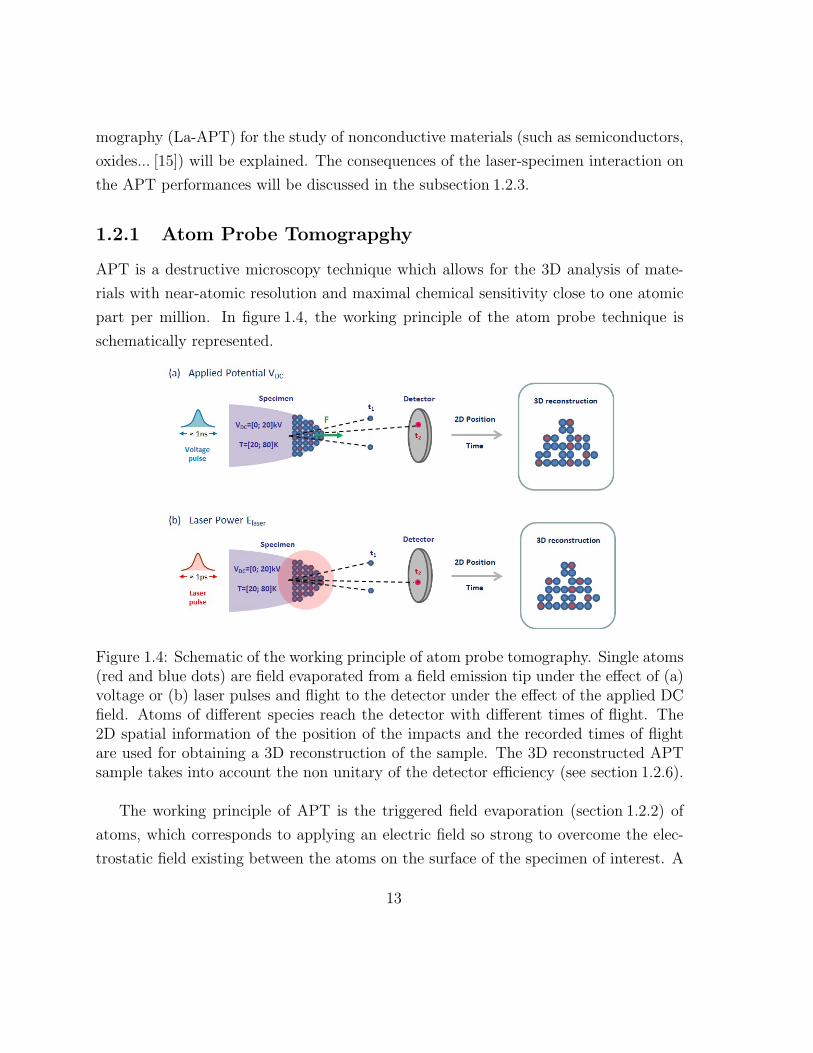
1.2.1 Atom Probe Tomograpghy
APT is a destructive microscopy technique which allows for the 3D analysis of mate-
rials with near-atomic resolution and maximal chemical sensitivity close to one atomic
part per million. In figure 1.4, the working principle of the atom probe technique is
schematically represented.
Figure 1.4: Schematic of the working principle of atom probe tomography. Single atoms(red and blue dots) are field evaporated from a field emission tip under the effect of (a)voltage or (b) laser pulses and flight to the detector under the effect of the applied DCfield. Atoms of different species reach the detector with different times of flight. The2D spatial information of the position of the impacts and the recorded times of flightare used for obtaining a 3D reconstruction of the sample. The 3D reconstructed APTsample takes into account the non unitary of the detector efficiency (see section 1.2.6).
The working principle of APT is the triggered field evaporation (section 1.2.2) of
atoms, which corresponds to applying an electric field so strong to overcome the elec-
trostatic field existing between the atoms on the surface of the specimen of interest. A
13

sufficient positive electric field (∼10 V/nm) generates the emission of atoms from the
material surface. To create this strong electric field, the positively polarized samples
need to have a needle shape, with an apex radius < 100nm. The atoms evaporated from
a needle-shaped specimen are finally detected on a position- and time-of-flight-sensitive
detector. The position on the 2D detector along with the knowledge of the evaporation
order allow reconstructing the 3D position of detected atoms within the reconstructed
volume, while their chemical nature can be deduced by time-of-flight spectroscopy (sec-
tion 1.2.4) of the ions accelerated by the constant electric field. The field evaporation
of the ions can be triggered in two ways: by voltage pulses or by laser pulses. In the
voltage pulse mode, the evaporation probability of the most protruding ions is greatly
increased by the superposition of potential pulses with a temporal width of the order of
few ns to the constant potential applied to the sample. The additional field lowers the
energy barrier confining the surface atoms so that for the short duration of the pulse
the evaporation rate is higher. In laser pulse mode, the ion evaporation is triggered by
the interaction with the specimen of a pulsed laser, with sub-ps pulses duration, whose
main effect is to locally increase the specimen surface temperature in a phonon mediated
absorption process and thus temporarily increasing the thermal energy of surface ions,
increasing their probability of tunneling through the confining energy barrier or passing
over it [16, 17]. It is worth noting that the voltage pulse mode allows for the analysis
of metallic systems only, as in non-conductive systems the pulses are strongly distorted
(lowered maximal amplitude and longer duration) so that they are no longer able to
properly trigger the field evaporation. The introduction of the laser pulse operating
mode, and of the so-called laser assisted atom probe tomography (La-APT), opened to
the possibility of analyzing high resistivity materials such as semiconductors [18], ox-
ides [19] and polymers [20]. In the following, the main aspects and features of APT are
discussed in more details: the physics governing the field evaporation of atoms is de-
scribed within the context of APT experiments. Different APT operating modes, along
with the way in which the chemical and structural information is extracted by APT
data are also discussed. Different involved resolutions and detection capabilities are
considered. Finally, the methods and numerical tools used for exploiting the structural
information within the correlative approach are reported.
14

1.2.2 Physics of field evaporation
The field evaporation of ions from the surface of materials, under the effects of strong
electric fields, is the physical phenomenon underlying the triggered evaporation and
consequent detection of charged particles (atoms and molecules), during APT analy-
ses. The relationship between the applied potential and surface field is given by the
equation (1.1):
F =V
kf ·R(1.1)
where R is the surface curvature radius and kf is the field factor, a semiconstant which
accounts for both the geometry of the emitter and its electrostatic environment. The
particular geometry of field emission tips (R ∼ 50nm) allows for the creation of surface
fields strong enough for deforming the most external atomic layers to a point in which
atoms can leave the surface as ions. From the point of view of one of the protruding
atoms, this can be seen as a barrier-crossing process, which can thus be empirically
described by the following Arrenius-like crossing rate:
K = ν0 · exp(
− Q(F )
kB · T
)
(1.2)
where ν0 is the vibration frequency of the evaporating atom and Q(F ) defines the
field depending energy barrier. A relative simple 1D classical description of the energy
barrier was proposed by Muller [21] as the difference between the surface atom binding
energy Λ and the maximum potential energy of an ion close to the surface UMAX . The
ion potential energy as a function of the distance from the surface can be written as:
U(z) =
(
∑
In − n · φ)
− n2 · e216 · π · ε0 · z
− n · e · F · z (1.3)
where
(
∑
In − n · φ)
is the energy necessary for ionizing the atom (In and φ being
respectively the n-th ionization energy and the electronegativity of the surface). The
second term describes the attractive potential induced by the ion electrostatic image
and the third term is the repulsive electrostatic force caused by the positive applied
15

field. The maximum potential energy of the ion can be written as:
UMAX =
(
n3 · e3 · F4 · π · ε0
)1/2
(1.4)
so that the energy barrier Qn(F ) is:
Qn(F ) =
(
Λ +∑
In − n · φ)
−(
n3 · e3 · F4 · π · ε0
)1/2
(1.5)
where Λ is the bonding energy of the surface atom. From the equation (1.5), the
evaporation field Fevap, corresponding to Qn = 0 can be defined as:
Fevap =4 · π · ε0n3 · e3 ·
(
Λ +∑
In − n · φ)2
(1.6)
for F ≈ Fevap, the equation (1.6) can be rewritten as:
Qevap,n(F ) =Q0,n
2·(
1− F
Fevap
)
(1.7)
where Q0,n = Qn(0) =
(
Λ+∑
In−n·φ)2
. While being able to reproduce experimental
results in some particular cases, this model is not able to fully grasp the complexity of
field evaporation processes, its main drawbacks being the lack of a realistic modeling of
the potential seen by the evaporating atom close to the surface and the fact that the
distribution of the local surface electric field is not taken into account. More realistic
models describe the way in which under the effects of the field the surface is deformed,
leading to a continuous variation of the charge carried by the atoms undergoing the
field evaporation process. More precisely, surface (protruding) atoms can be described
as partial ions subjected to a field-induced Maxwell stress, defined as:
fM =ε0 · F 2
2(1.8)
16
caused by the intrinsic inter-repulsion of surface charges, so that the potential barrier
which has to be crossed by the ions can be seen as due to contributions from a clas-
sical atomic energy barrier (universal binding energy curve [22, 23]) or an analytically
estimated atom/surface pair potential (Morse potential [24]), and the electrostatic po-
tential of the field-dependent ion partial charge q(F ). A complete description of the
phenomenon should also take into account the 3D atomic configuration characterizing
the surroundings of the evaporating atoms (modifying the local potential), along with
the effects of temperature and surface diffusion, contributions which can be studied by
different approaches such as molecular dynamics simulations [25, 26]. During an APT
experiment, atoms are evaporated from a surface whose characteristics are determined
by the crystallography of the system and by the sample preparation process. The most
protruding atoms are those subjected to the highest surface field and consequently those
with the highest probability of being field evaporated. This behavior can be described
by rewriting the evaporation rate considering equations (1.2) and (1.7) as the following
relationship:
K = N ′ · ν0 · exp(
− C · (1− F/Fevap)
kB · T
)
(1.9)
where C = Q0/2 and N ′ defines the number of atoms which feel a surface field which is
high enough for triggering their field evaporation. The given relationship is valid until
F is equal to 20% of Fevap, while for less intense electric fields, this relationship is not
valid. The rate defined in equation (1.9) is not directly observed in experiments, as the
reduced field of view of the instrument and the non-unity detection efficiency influence
the detection rate. The equation 1.9 was expressed in terms of Fevap, the extrapolated
voltage value for which atoms can be evaporated at a good rate at T = 0 K. For a
given surface field, when the temperature of the system is increased, the evaporation
rate also increases, as the atoms can cross the energy barrier by thermal activation. It
can thus be convenient defining the quantity FT which corresponds to the threshold
surface field for T 6= 0 and for a fixed rate KT [27] as:
FT
Fevap
= 1− T ·[
kBC
·(
N ′ · ν0KT
)]
(1.10)
17

where the slope of the linear dependence on T depends on the atom binding energy
through C (variations from linearity can be experimentally observed [28] because the
binding potential form from which the equation (1.10) is derived relies on a certain
number of approximation). In the next section, the laser-assisted field evaporation
mechanism is addressed.
1.2.3 Laser-induced field evaporation
The laser/matter interaction which is at the core of La-APT is a complex phenomenon
which involves different physical processes depending on the nature of the analyzed
material, on the geometry of the specimen and on the constant DC field applied to
it. As previously introduced, the main merit of La-APT is allowing analyzing material
systems for which the voltage pulse triggering of ions field evaporation is not possible.
Nevertheless, the laser pulse operation mode can be extremely useful for applications
in the study of metallic materials, as it can ensure better performances with respect
to electrical APT in terms of mass resolution and field of view at condition that the
illumination conditions are properly tuned [29]. From the point of view of La-APT,
the main difference between metallic and non metallic materials is the way in which
they interact with light: in metals, photons excite electrons to higher levels within
the half-filled conduction band. These eventually thermalize to lower states interacting
with other electrons or phonons, increasing the temperature of the system. In semi-
conductor systems the electron-light interaction is more complex, as it reflects their
complex electronic structure. The analyzed specimen is more or less transparent to the
incident laser (the light penetration depth is also affected) depending on the photon
energy and bandgap. Also for semiconductors the absorption of light leads to the in-
creasing of the system temperature, as generated charge carrier pairs recombine through
phonon-mediated processes. Additional complexity stems from the particular geometry
of APT specimens, this being related to the capacity of the system to locally absorb
light. Nonuniform absorption maps can be obtained solving the Maxwell’s equations
for the 3D field emission tips volume, showing that depending on the material and
on the laser direction and properties, photons can be absorbed in preferential posi-
18

tions on the surface (metals and semiconductors) and within the bulk with complex
distributions of absorption spots (only semiconductors). The applied surface field also
influences the absorption properties of the sample, as it affects the band structure at
the sample/vacuum interfaces. The physical effects which enter in play in the different
mentioned cases along with the effects of different fields and laser properties will not be
discussed here in more detail. For more detailed information refer to [30, 29, 31, 32].
1.2.4 Time-of-flight mass spectroscopy
Within an APT analysis, after having left the surface, a field evaporated ion is subjected
to the strong electric field induced by the potential difference VDC existing between the
specimen surface and the detector. The kinetic energy of the evaporating ion can be
considered to be null only after the crossing of the energetic barrier. Under the effects
of the acceleration induced by the electric field, the ion acquires a kinetic energy which
equals the electrostatic potential corresponding to VDC :
1
2·m · v2 = n · e · VDC (1.11)
and thus starting to flight towards the detector at speed:
v =
(
2 · n · e · VDC
m
)1/2
(1.12)
Typical applied potentials range between: VDC = [1; 20] kV, the ion acquires the total
kinetic energy given by (1.11), within a distance from the surface which is negligible
with respect to typical flight lengths (specimen-detector distance) L = 0.1 − 0.5m, so
that the ion can be considered as flying with unchanged velocity along all the flight path.
The time-of-flight (TOF) of the ion, corresponding to the time needed for traveling from
the surface to the detector can then be easily derived as:
t = L ·(
m
2 · n · e · VDC
)1/2
(1.13)
19

During an APT acquisition, the elapsed time tm measured between the generation of
the laser pulse and the detection of each event is registered (typically within the [1; 5]µs
range), so that for each ion the mass over charge ratio M is established:
M =m
n= 2 · e · VDC ·
(
tmL
)2
(1.14)
allowing associating at each detected ion its chemical species. The histogram of all
measured M values define what is referred to as mass spectrum. Mass spectra are
characterized by peaks which can be ascribed to ions with corresponding mass over
charge ratio, evaporated during a triggering pulse (peaks indexing). Ions evaporated
in-between pulses constitute the background noise of the spectrum. The mass resolu-
tion of the technique is directly related to the broadening of the peaks which is affected
by several dfferent contributions, both instrumental and related to the physics of field
evaporation. Mass spectra are optimized by means of statistical corrections which take
into account different contributions, such as the different flight paths on different posi-
tions of the detector and the varying voltage applied to the tip. Further discussion of
the calibration of the instrument, the different sources of incertitude for the determina-
tion of M and the corrections used for optimizing the mass spectra is beyond the aims
of this thesis. For more detailed information on these topics refer to [33]. Depending on
the analyzed material, mass spectra of different complexity from the point of view of
their interpretation can be obtained. Ideally, there should not be overlapping between
peaks associated to different ion or molecular species. If they do overlap, the relative
contributions to single peaks still might be estimated by their deconvolution on the
basis of the isotopic abundancies of different chemical species.
1.2.5 Three-dimensional reconstruction of APT data
The APT ability to analyze the 3D structure of materials relies on the capacity of
transforming the 2D information of the impact positions on the detector of the field
evaporated ions and the temporal information consisting in the ordering of their arrival
in the 3D information consisting of the original position of the detected ions within the
20

reconstructed specimen volume. In other words, the 3-dimensional reconstruction pro-
cedure of APT data reduces to passing from the data triplet associated to each detected
event (X; Y ; n), whereX and Y are the position coordinates on the detector of the
n-th detected ion, to the set of values (x; y; z), corresponding to the coordinates within
the Cartesian reference system of the reconstructed space. The simplest transformation
procedure [34] is based on the definition of a magnification parameter η which describes
the magnification of the specimen surface image on the detector, for which:
x = X/η (1.15)
y = Y/η (1.16)
Within the approximation of small fields of view, the following simplified expression for
the magnification M can be used:
η =L
ξ · r (1.17)
where L is the estimated distance between the specimen surface and the detector, r
is the surface radius of the sample and 1 < ξ < 2 is a projection parameter which is
commonly referred to as image compression factor and which takes into account the
detection of the ions trajectory (initially perpendicular with respect to the surface)
close to the surface induced by the surface field. Consequently, x and y follow from the
detector impact coordinates as:
x =X
L· ξ · r (1.18)
y =Y
L· ξ · r (1.19)
This simple 2D reconstruction method (point projection reconstruction) for the lateral
coordinates of the evaporated ions is schematically represented in figure 1.5 (a). The z
coordinate of the i-th ion in reconstructed space is determined considering a variation
in its position along the z-axis with respect to the i-th event of:
dzi =vatiη · s =
vati ·M2
η · S =vati · L2
η · S · ξ2 · r2 (1.20)
21

where vati is the atomic volume of the i-th atom within its specific phase, s is the cross
Figure 1.5: Schematic rapresentation of (a) the 2D point projection reconstructionmethod. In (b), the deflection of ion trajectories due to the applied field are represented,along with the angles α1 and α2 which defines the field of view of the technique.
sectional area of the specimen corresponding to the detector area S and η is the detec-
tion efficiency of the corresponding ionic species (note that in reconstruction algorithms
often an average or phase-related detection efficiency is considered instead). The set
of equations (1.18), (1.19) and (1.20) should in principle allow for obtaining the full
3D reconstruction of the atomic positions, given the knowledge of the sample related
parameters vati and r along with the instrument and experimental conditions related
parameters L; S; ξ and η. Nevertheless, for obtaining more realistic reconstruction bet-
ter transfer functions relating detector to reconstructed space coordinates are needed.
In APT data treatment, transfer functions relying on a certain number of assumptions
above the geometrical shape of the sample and the electrostatic field distribution are
used, allowing to overcome the limitations imposed by the small field of view approx-
imation [15]. In order for a transfer function to be able to properly reconstruct more
than a few atomic layers, it has necessarily to take into account the fact that during
the field evaporation the radius of the specimen increases (this holds also for the simple
procedure described here). The evolution of r is commonly estimating from the voltage
applied to the tip considering:
F = β · VDC (1.21)
where F is the surface field and β is the field-to-voltage conversion factor, along with
eq. (1.1). The parameter kf , which appears in eq. (1.1), can be estimated if r for a
specific applied voltage is independently determined experimentally (e.g. by Scan-
ning Electron Microscopy ‘SEM’ or Transmission Electron Microscopy ‘TEM’). This
22
reconstruction method (commonly referred to as Eβ algorithm) leads to reconstruction
artifacts when systems containing phases with different evaporation fields are consid-
ered. In this case, the evolution of r is usually better accounted for by assuming a
specific geometry of the specimen and use geometrical models for determining the re-
lationship between r and dzi. Algorithms commonly used consider a hemispherical
surface mounted over a cone described by a shank-angle and an initial radius (cone
angle reconstruction method [35, 36]), or over more complex structures whose geometry
is assessed by electron microscopy techniques (tip-profile method). When considering
semiconductor heterostructures, information on the structure of the system issued by
other microscopy techniques is extremely useful as it allows tuning the reconstruction
parameters in order to obtain the best possible reconstruction (e.g. case of planar
layers in multi-layered heterostructures [37]). A general quantification of the spatial
resolution of the technique is not easily obtained as the resolution of the detection sys-
tems contributes only marginally to the real capabilities of APT to resolve the position
of atoms within the reconstructed space. In fact, the nature of the field evaporation
processes and the reconstruction methods are the limiting factors to the spatial reso-
lution. Modern delay line detectors have a spatial resolution (defined as the capacity
of distinguishing between two spatially close events on the detector) of the order of
[50; 100] µm [38]. Considering typical magnifications of atom probes, this results in a
spatial resolution on the plane perpendicular to the reconstruction axis lower than 5 A.
On the other hand, the effective resolution on the xy plane is considerably lower due
to the contribution of three main effects:
1. The initial transverse velocity of field evaporating atoms can be different from
zero [39], due to thermal agitation at which adatoms are subjected to;
2. When an atom leaves the surface within the evaporation process, its trajectory is
influenced by the local atomic configuration of the surface and the corresponding
local distribution of field [40];
3. Before being effectively evaporated, atoms can diffuse along the surface (normally
high laser energies are needed [41]) or simply interact with neighbor atoms (while
23

still not being evaporated), slightly modifying their position and thus the flight
trajectory (rolling-up motion [42]).
Due to these effects , experimentally observed lateral resolutions are of the order of 1nm.
The ideal spatial resolution along the z-direction is given by equation (1.20) (the inter-
distance between successive reconstructed atomic planes) and thus depends on the aver-
age atomic volume of the atoms in the crystal and on the detection efficiency. It follows
that for typical values of vat and η the ideal in-depth resolution is less than one pm.
The real spatial resolution is again considerably lower. The limiting factor in this case
is the probabilistic nature of the field evaporation phenomena, or more precisely the
fact that an uncertainty in the order of evaporation of atoms exists: an atom subjected
to the highest local surface field is not necessarely field evaporated before other atoms
subjected to lower field. Considering the number of surface atoms N within a typical
tip and the relative rate with which the highest surface field atom is evaporated after
n other atoms [43]:K(n)
K= exp
(
2 · C · nkB · T ·N
)
(1.22)
this uncertainty can be of the order of hundreds of atoms, leading to nearatomic in-
depth resolution. It should be noted that what has been said about the APT spatial
resolution actually holds for systems constituted by a single phase. The semiconductors
considered in this thesis are constituted by regions characterized by different composi-
tions and consequently different evaporation fields. During evaporation, regions with
different evaporation fields evaporate with different rates, so that the spatial resolution
along all direction is affected: local modifications of the specimen surface induced by
the preferential evaporation of specific phases [44, 45, 46] can modify the surface field
distribution and consequently the trajectories of evaporating ions, deteriorating the
in-plane resolution (e.g. see the local magnification artefact [43, 47] affecting the recon-
struction). This issue will be discussed more in detail for the analyzed heterostructure
ZnO/MgZnO in section 5.2.2 of Chapter 5. while the in-depth resolution is affected
by the uncertainty in the evaporation order which follows different evaporation fields.
24

1.2.5.1 Delay line detector (DLD)
In a conventional DLD systems, as the one used in this work, the electron clouds
generated by Multi Channel Plates (MCPs) are received on the two delay lines X and
Y, producing each one two analog signals travelling in opposite directions (fig. 1.6).
Figure 1.6: Detection dynamic in a conventional DLD system: (a, b, c) an ion impactat the top of the first MCP generates electrons, which are multiplied with a cascademechanism inside the two MCPs. (d) The generated electronic cloud is extracted atthe bottom of the second MCP and absorbed by the DLD. (e) Two analog signals arepropagated along each delay line.
As the length of the two delay lines are fixed, the propagation times of the analog
signal in each delay line are well known. These strictly depend on the position of
electron cloud. In this way, four timing information provide the impact position (x, y)
of a detected ion. This position can be back-projected to the tip surface using specially
dedicated reconstruction algorithms, allowing to determine the ion position (x′, y′) on
the tip volume. The spatial resolution obtained by a conventional detector is closed
to 80 µm on the MCP surface, which approximately corresponds to less than 1A on
the tip surface. The evaporation order of atoms allows access to the third dimension
z′. Detailed information about the reconstruction algorithms are provided in ref. [15].
In order to determine the TOF, so the chemical nature of detected ions, a fifth time
difference must be measured. A detailed scheme of the electronic system used to convert
the analog signal in timing information in a conventional MCP/DLD is reported in
fig. 1.7.
An analog signal produced by the MCP/DLD is amplified and then transformed
in a digital signal by a discriminator. A logic value “1” is generated by this device
when the input signal is higher than a fixed threshold value. Lastly, the digital signal
25

Figure 1.7: Scheme of the electronic system used to measure the impact position of theions on the MCP in a conventional MCP/DLD.
is send to a Time-to-Digital Converter (TDC) which calculates the time difference
between two digital signals. The first one it provided by a photodiode and starts
the timing measurement in correspondence of the arrival of a laser pulse on the tip.
The second signal is the one generated by the discriminator, which stop the timing
measurement. The TOF interval of an ion corresponds to the time difference between
the signal provided by the photodiode (reps. the departure time from the tip) and
the signal generated by the MCPs. Clearly, all the timing delays due to the electronic
system and the signal propagation on the DLD are taken into account to calculate the
TOF. Conventional DLD detectors can provide information for multiple ion impacts.
Serial multiple ion impacts corresponding to the arrival of two or more ions which can
be detected is their TOF difference is larger than ∼ 4ns. This value corresponds to the
Time Resolving Power (TRP) of the DLD detector. Differently, simultaneous impacts
correspond to the arrival of two or more ions with almost the same TOF. If the impact
distances on the MCP are lower than the Spatial Resolving Power (SRP), which is
∼ 4mm in a DLD detector (corresponding to ∼ 4 ÷ 0.4 nm on the tip surface), the
signals generated by each ion on the delay lines appear overlapped. Therefore, a single
signal, resulting for the superimposing of several signals generated by each ion impact
is amplified. In this case, only one digital signal is generated by the discriminator
and sent to the TDC (fig. 1.8(a)). This means that only one impact is detected and
the event is recorded as a single ion impact. Nowadays, the detection of multiple
26

Figure 1.8: (a) Example of the analog-to-digital conversion carried out by the discrim-inator. A signal consisting of two overlapped peaks separated 4 ns is associated to thedetection of simultaneous impacts of two different ions. With a treshold equal to the50% of the peak value (blue dashed line), only one 5ns width digital signal is generated(in red). (b) Example of an analog signal (black line) collected on the delay line andprocessed by an aDLD. The deconvolution of the analog signal reveals two differentsignals (red and green lines) associated to the simultaneous impact of two ions.
ion events has been improved through the design of an advanced Delay Line Detector
(aDLD) [48, 19], which allows decreasing both the Time Resolving Power (TRP) and
the Spatial Resolving Power (SRP) to 1.5ns and 1.5mm (corresponding to ∼ 1÷0.1nm
on the tip surface), respectively,showed in fig. 1.8(b). As a consequence, the detection
of multiple ion events is strongly improved.
Therefore, the performance of the experimental system used in this work can be further
improved substituting the DLD with an aDLD.
1.2.6 Field of view and detection efficiency
Not all the atoms which are field evaporated from the tip specimen during an APT
acquisition participate to the mass spectrometry analysis and/or to the tomographic
reconstruction process. Among those which are not evaporated during a voltage/laser
pulse and successfully detected, some are accelerated by the surface field towards the
detection system but their trajectory ends outside the acceptance angle of the detector.
The maximum size of the object that can be observed is defined by the field of view
of the instruments. The field of view is defined as a function of three different values,
27

corresponding to: x, y (lateral directions) and z (depth direction). The length of the
specimen which can be proved by the technique depends on:
a. the geometry of the sample (shank angle), determining the depth of analysis
reached before obtaining the maximal tip radius for which a surface field evapo-
ration is attainable;
b. the maximum DC potential applicable to the sample;
c. the evaporation field of the system (which again is related to the maximum radius
at which atoms can be field evaporated).
The lateral field of view depends on the characteristic of the instruments such as the
flight length and the surface of the detection system, but is also influenced by experimen-
tal conditions, namely by the applied potential which modifies the ions trajectories [15].
It is commonly defined for an instrument by means of the 2 angles represented in fig-
ure 1.5 (b), namely the acceptance angle of the detector with respect to the sample α1,
and the angle which subtend the section of the surface imaged on the detector with
respect to the center of the hemispherical tip head α2. Note that the second angle is
bigger as the trajectories of the ions leaving the surface are bent in the direction of the
detector in the first steps of flight. The total probed volume by a single APT analysis
corresponds to the imaged part of field emission tips with apex radius smaller than
200 nm and for depths lower than 1 µm. This implies that the features to be analyzed
have to be characterized by typical size-scales comparable to the probed volume. When
analyzing APT data, the atoms which are evaporated outside the field of view of the
detector present no particular problems, as they are simply excluded from the TOF
spectra and the reconstructed volume. Much more care is needed when taking into ac-
count those ions which are evaporated within the field of view but are not detected, for
different ion loss mechanisms (e.g. because evaporated in-between the triggering pulses
and end up the background noise of the mass spectra). The ensemble of the ions loss
mechanisms are schematically represented in figure 1.9. The relative amount of ions be-
longing to the first category is quantified by the multi-channel plate detection efficiency
ηMCP , which defines the fraction of atoms which hit the detector, but that are stopped
28

Figure 1.9: Schematic rapresentation of the ions loss mechanisms. Only 60-80 % of theions evaporated within the field of view are actually detected.
by the edges of the micro-channels and which does not lead to the generation of a
detectable electric signal. This geometrical constraint fixes the ideal APT detection ef-
ficiency at ηMCP ≈ [60; 80]% . The actual detection efficiency, entering equation (1.20),
is lower, the difference being mainly ascribable to the ions which are not evaporated si-
multaneously with the arrival of the voltage/laser pulse and for which the identification
of the chemical nature is not possible (not indexed in the mass spectrum). The total
detection efficiency η thus should account for both effects. Other mechanisms leading
to the loss of atoms have been proposed for explaining experimental results obtained
on semiconductor systems, such as the field evaporation of neutral molecules [49, 50]
(which are thus not accelerated towards the detector, see section 1.2.7) or their for-
mation as the product of dissociation processes [51] (which are either not detected or
detected with random TOFs). It should be noted that the probability for an atom of
being evaporated in-between pulses or as a part of a neutral molecule depends on its
chemical nature. It follows that a better description of the detection process is given
by a specific detection efficiency, as in the equation (1.23):
ηi = ai · ηMCP (1.23)
29

where ai defines the fraction of atoms of species i which are field-evaporated as ions
during the voltage/laser pulse. The effects of different detection efficiencies on the
measurements of composition performed by APT, along with a more detailed discussion
of loss mechanisms and quantification of η can be found in the next subsection 1.2.7.
1.2.7 Compositional measurements and related issues in APT
While the composition of a given specimen can be determined by counting the events in
the mass/charge histogram, various artifacts and aberrations may affect APT analysis.
They originate from various sources (detection issues, presence of interfaces, clusters,
layers with different evaporation field Fev in the material, reconstruction algorithms).
All these artifacts have important consequence on both compositional measurements
and 3D reconstructions.
1.2.7.1 Mass spectra indexation
In order to determine the measured composition it is necessary to identify each peak
in the mass spectrum. In presence of molecular ions this can be quite complex, but
a correct and unambiguous interpretation of the mass spectrum is very often possible.
However, two particular cases lead to an incorrect interpretation of the mass spectrum:
1. if we call an element A and m its atomic mass, then it is impossible to distinguish
the detection of the An+ from the A2n+2 , since the mass to charge ratio is the same
one;n is an integer index.
2. if we consider two species with the same mass/charge ratio, it is not possible to
associate specifically to each peak the exact nature, but only the probability to
be associated to one of the species: e.g. %(A), for the first one, and e.g.%(B), for
the second one.
In summary, in the case (1) to know the chemical specie, of the detected atoms, is
possible, but not their exact number. In the case (2) to know the exact number of ions
to associate to each peak is possible, but not their chemical nature.
30
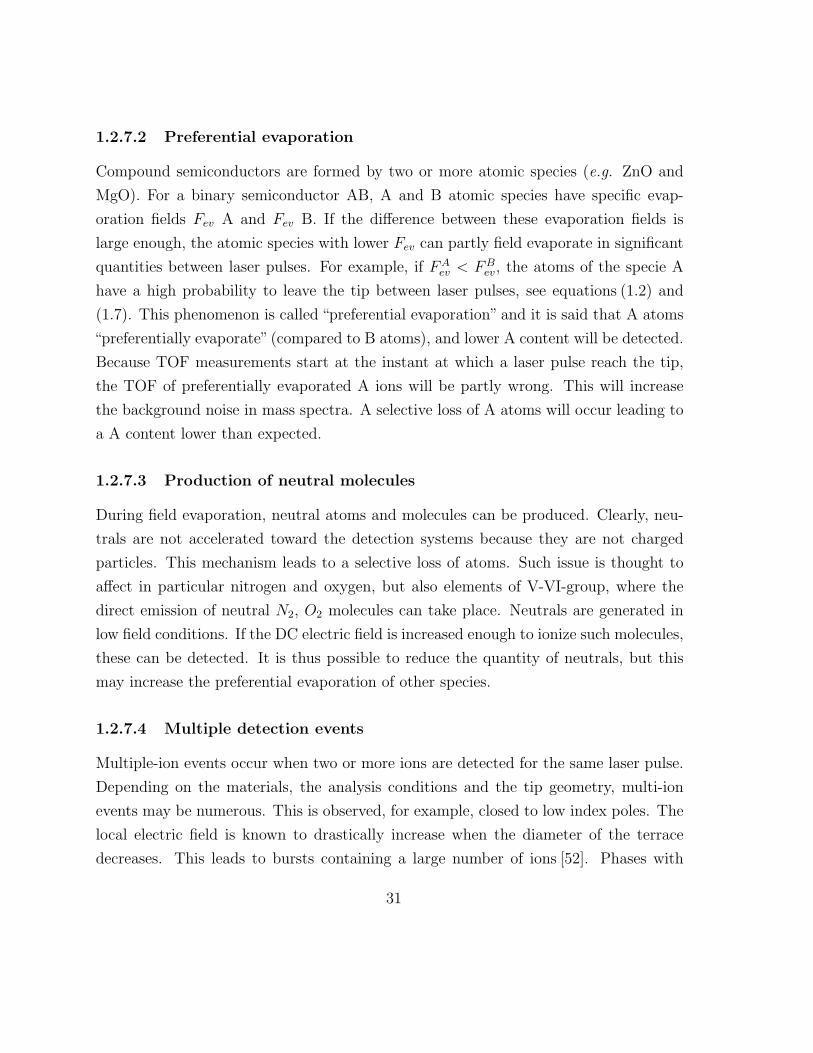
1.2.7.2 Preferential evaporation
Compound semiconductors are formed by two or more atomic species (e.g. ZnO and
MgO). For a binary semiconductor AB, A and B atomic species have specific evap-
oration fields Fev A and Fev B. If the difference between these evaporation fields is
large enough, the atomic species with lower Fev can partly field evaporate in significant
quantities between laser pulses. For example, if FAev < FB
ev, the atoms of the specie A
have a high probability to leave the tip between laser pulses, see equations (1.2) and
(1.7). This phenomenon is called “preferential evaporation” and it is said that A atoms
“preferentially evaporate” (compared to B atoms), and lower A content will be detected.
Because TOF measurements start at the instant at which a laser pulse reach the tip,
the TOF of preferentially evaporated A ions will be partly wrong. This will increase
the background noise in mass spectra. A selective loss of A atoms will occur leading to
a A content lower than expected.
1.2.7.3 Production of neutral molecules
During field evaporation, neutral atoms and molecules can be produced. Clearly, neu-
trals are not accelerated toward the detection systems because they are not charged
particles. This mechanism leads to a selective loss of atoms. Such issue is thought to
affect in particular nitrogen and oxygen, but also elements of V-VI-group, where the
direct emission of neutral N2, O2 molecules can take place. Neutrals are generated in
low field conditions. If the DC electric field is increased enough to ionize such molecules,
these can be detected. It is thus possible to reduce the quantity of neutrals, but this
may increase the preferential evaporation of other species.
1.2.7.4 Multiple detection events
Multiple-ion events occur when two or more ions are detected for the same laser pulse.
Depending on the materials, the analysis conditions and the tip geometry, multi-ion
events may be numerous. This is observed, for example, closed to low index poles. The
local electric field is known to drastically increase when the diameter of the terrace
decreases. This leads to bursts containing a large number of ions [52]. Phases with
31

very different evaporation fields may also produce numerous multi-ion events. The
preferential retention of high evaporation field species at the tip surface is then observed.
Burst containing large numbers of high evaporation field ions can occur, generating
multiple-ion events. An example is provided by G. Da Costa et al. [38], analyzing
[100] oriented Si wafers where a very high dose of 11B atoms were implanted (1017 at ·cm−2). Because the evaporation field of B (64 V · nm−1) is higher than that of Si
(33 V · nm−1), B is prone to strong retention effects. Even when a low detection
rate is used (0.006 event/pulse), burst involving B ions are observed. The use of a
conventional DLD detector leads to a selective loss of B atoms due to pronounced pile-
up effects. Contrariwise, using an aDLD detector (section 1.2.5.1) up to 30 ions on the
same evaporation pulse can be detected. The ability to detect multi-ion events is in
fact fundamental in order to measure the correct composition.
1.2.7.5 Dissociation phenomena
Dissociation of molecular ions may occur during their flight. This reaction is schema-
tized in figure 1.10, where a mother molecular ion mp is dissociated in two daughter
ions m1 and m2. Clearly, both total mass and charge must be conserved during this
process. Because daughter ions are typically charged particles, these are accelerated by
the electric field and can be detected. However, the measured TOFs of daughter ions
are different from these expected for the direct mechanism of evaporation. Dissociation
processes can be revealed thanks to the so-called correlation histograms [53]. These his-
tograms represent the m1, m2 ion couples detected in multiple-ion events. Multiple
events with n > 2 were taken into account along with the possible permutations of
ion pairs involved in these events: e.g. a triple event, where m1, m2 and m3 ions are
involved and split in m1, m2 , m2, m3 and m1, m3 ion pairs (multiple-ion
events with n > 2 are very few). The ion-pair order is not considered and the his-
togram is computed by imposing a diagonal symmetry. Ions can leave the tip exactly
in coincidence with laser pulses, leading to the detection of multiple events in which
ions exhibits the expected mass-to-charge ratios.
A simple model of molecular ion dissociation is proposed in ref. [53]. A molecular parent
32
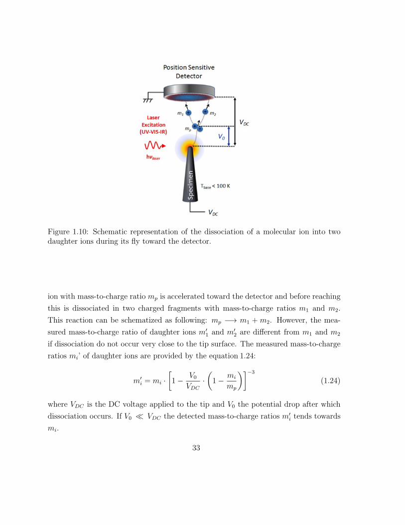
Figure 1.10: Schematic representation of the dissociation of a molecular ion into twodaughter ions during its fly toward the detector.
ion with mass-to-charge ratio mp is accelerated toward the detector and before reaching
this is dissociated in two charged fragments with mass-to-charge ratios m1 and m2.
This reaction can be schematized as following: mp −→ m1 +m2. However, the mea-
sured mass-to-charge ratio of daughter ions m′1 and m′
2 are different from m1 and m2
if dissociation do not occur very close to the tip surface. The measured mass-to-charge
ratios mi’ of daughter ions are provided by the equation 1.24:
m′i = mi ·
[
1− V0VDC
·(
1− mi
mp
)]−3
(1.24)
where VDC is the DC voltage applied to the tip and V0 the potential drop after which
dissociation occurs. If V0 ≪ VDC the detected mass-to-charge ratios m′i tends towards
mi.
33

1.2.8 Charge State Ratio metrics
In this thesis, we adopted the so-calledMe2+/Me1+ Charge State Ratio (CSR) metrics,
which was enunciated for metallic elements, but it can be considered valid also for
semiconductors. The main points which make advantageous to use the CSR metrics
are the following:
(i) The Me2+/Me1+ CSR is related to the surface field. This relationship might be
made quantitative through Kingham’s post-ionization model [54]. In principle,
the phenomenon of post-ionization takes place at a distance of several A from
the sample surface, and should be nearly independent of the material in which the
atom was found if the evaporation takes place in the singly charged state. The
charge state abundances of the evaporated ions are thus a function of the surface
field. By inverting this function, it becomes possible to calculate an effective
surface field Feff . However, this effective field Feff should only be considered as
an estimate of the actual surface field FS introduced in eq.(1.1) [55, 56].
(ii) The Me2+/Me1+ CSR can be defined as a local quantity, as it can be calculated
within arbitrarily chosen 3D volumes. This is useful in order to map the local
surface field and correlate it with the locally measured composition.
(iii) TheMe2+/Me1+ CSR allows for studying the composition trends even in the case
where the tip shape significantly changes during the APT analysis.
1.3 La-APT/µPL coupled “in-situ”
In the first two sections (1.1 and 1.2) we have described separately the working principle
of two independent techniques: the µPL and the (La-)APT systems. In this thesis the
La-APT and µPL spectroscopy were combined “in-situ”, within the same instrument.
The combination of these two techniques was made with the aim to use an original
multi-microscopy approach, which allows to better correlate and understand the physics
involved in field-evaporation process and the emissive properties of the nanomaterials
probed under a high electric field (≥10 V/nm). The advantage of this new machine is
34

to use the same laser excitation for both evaporating a tip specimen and for inducing
the emission (µPL emission) which can be detected while the sample is evaporating, as
it is shown in figure 1.11. This process allows to strictly correlate the variation of the
Figure 1.11: The core of the project: the combination between La-APT and the µPLsystems used to probe the sample under high electric field.
photoluminescence signal with nano-metric scale volumes of the tip evaporated during
APT. Thanks to the development of a specially designed tomographic atom probe, it
is shown that µ-PL can be successfully performed on a single atom probe tip during
La-APT. In principle, the emission of single quantum light emitters (e.g. single QW
or QD) or optically active defects can be revealed. This method can be extended to
a wide range of bandgap materials, opening new perspectives for correlative studies
of single atom probe tips. In this thesis, the “in-situ” configuration of the system
setup was used in two different ways, in order to study two different materials: single-
crystal diamond nanoneedles containing color centers and ZnO/MgxZn1−xO MQW
heterostructure specimens. These two different methods will be described more in
details in Chapter 3 and Chapter 5, respectively, below, the general working principle
of the coupled system setup is introduced.
1.3.1 Experimental setup
A schematic representation of the combining µ-PL and La-APT is shown in figure 1.12.
In a conventional La-APT machine the tip is illuminated by laser pulses which trigger
35

the emission of ions (figure 1.4 (b)).
Figure 1.12: Schematic of the experimental setup: the coupled La-APT/µPL “in-situ”.
The absorption of laser pulses can generate µPL emission from the tip. In a conven-
tional APT instrument no optical elements are present in order to collect such signal. In
this system a spherical mirror is introduced inside the analysis chamber, following the
design proposed by Rigutti et al. [57]. The focal point of the mirror is in correspondence
of the tip. Such configuration allows collecting the µPL emission and focusing it outside
the atom probe analysis chamber, where: a spectrometer, with a spectral resolution of
0.06 nm, and/or a streak camera, used to measure the variation in time of the µPL
intensity, can be placed. In the specific: the instrument is equipped with a tunable
Ti:Sa laser which emits at 780 nm. A Third Harmonic Generator ‘THG’ (or Second
Harmonic Generator ‘SHG’) is employed to select a wavelength of 260nm (or 390nm).
The laser repetition frequency can be ranged between 400 kHz and 4MHz. The laser
is focused on atom probe tips with a spot size of around 1µm. The incident power can
be varied between 15µW to around 2000µW. A standard MCP/DLD detector is placed
in front of the tip at a distance of L = 17 cm. Such detection system is able to perform
36

analysis using laser repetition frequency up to 1.7MHz. This characteristic drastically
reduces the time required to perform La-APT compared to commercial tomographic
atom probe, where the laser repetition frequency is 50 or 100 kHz. Anyway, as men-
tionated in section 1.2.5.1, the detection system currently in use does not support the
detection of multiple-ion events due to difficulties related to the high acquisition fre-
quencies. The exclusion of multiple-ion events has a major impact on the compositional
measurements. In fact, in the semiconductor materials multiple-ion events are typically
about the 5 ÷ 20 % of the total number of detected events. The accuracy of composi-
tion measurements of binary and ternary semiconductors measured by La-APT, or the
coupled µPL/La-APT system, was demonstrated by E. di Russo et al. [58] to depend
mainly on the range of the surface electric field. In the article [58], the investigation of
the chemical composition of III-V and II-VI ternary alloys (AxB1−xC) gives a correct
value of the site fraction (x) at ‘low’ field conditions, while at ‘high’ field conditions a
preferential evaporation of mellic species was detected.
“In-situ”anlyses with the coupled system were performed on ZnO/MgxZn1−xO MQWs
systems and the experimental protocol followed in order to perform the correlative
analyses are reported in the section 5.2.1, Chapter 5. While, in the study of diamond
nanoneedles with color centers, the APT-detector is not used as a nanoanalysis tool,
but rather as position sensor for the laser spot, as it will be explained in the section 3.1,
Chapter 3.
1.4 FIB/SEM specimens preparation
The potential of the developed multi-microscopy approach relies on the possibility of
performing APT and µPL analysis on the same specimen. While the optical spec-
troscopy analysis has no particular requirements for what concern the geometry of the
tip, APT and electron microscopy require the samples to be prepared under the form
of field emission tips. Therefore, the µPL signals have to be acquired from specimens
whose optically active region is contained within the typical volumes of a field emis-
sion tip apex (radius of ∼ 50 nm and depth of few hundreds of nm), as explained in
section 1.3. The detection of the emitted PL signal could in principle be not an easy
37

task: let alone the difficulty which stems from the small volume of the emitting region
(which in principle can be coped with using a sensible enough detection system), the
main problem consists in the way in which specimens for APT and SEM analyses are
prepared.
In order to obtain the needed small apex radii, the heterostructure samples of ZnO/MgZnO
were prepared through Focused Ion Beam ‘FIB’ annular milling [59], for which high
energetic Ga ions are accelerated on the specimen surface following specific patterns
(ring-shaped patterns, from which the name of the technique is derived), removing
matter from the sample volume and sharpening it. The impinging ions can strongly
modify the properties of the surface and implant below the specimen surface at depths
which depend on their energy (or ion emission current) and consequently damaging the
optical properties of the system, creating non radiative recombination centers for the
generated charge carriers [60].
Figure 1.13: Non-radiative and radiative recombination process in annular milled fieldemission tips. (a) In single phase systems charge carriers generated in the bulk cantravel to the surface and recombine within non-radiative recombination centers. Inheterostructures, charge carriers can be generated in the bulk (b) or directly within theheterostructures (c) and then recombine radiatively within the heterostructures and farfrom the surface.
Notwithstanding the ion damage caused by the sample preparation procedures, a
good µPL signal could be obtained for all analyzed systems. While this result can
be partially ascribed to the caution exercised during the last milling steps (deposition
38

of a protective capping over the milled surface and milling performed at [1; 10] pA at
30 kV and 50 pA at 2 kV with an angle of incidence of around 4), the success of the
analysis relies on the confining properties of the nanostructured systems analyzed, as
schematized in figure 1.13: in specimens characterized by a single phase (a), charge car-
riers generated in the bulk can travel to the surface and recombine within non-radiative
recombination centers. In low dimensional semiconductors, depending on the nature
of the system and of the excitation energy (photon energy with respect to electron
and hole ground states energy difference), charge carriers can be generated in the bulk
(b), or directly within the heterostructures (c), and then recombine radiatively, within
the heterostructures, and far from the surface (as their diffusion length is diminished
by the quantum confinement provided by the heterostructures). The ZnO/MgZnO
MQWs specimens were prepared using the SEM-FIB NVISION40 (Zeiss) microscope.
The samples were prepared using the lift-out [61] and annular milling methods. On the
surface of the specimen a trench of∼ 20 µm length and ∼ 2 µm width is milled by FIB
and separated from the rest of the specimen by means of a micromanipulator. Sections
of this trench are cut and soldered on tungsten support tips by FIB deposition of Pt.
Finally, the needle-like shape for the soldered sections required for the multi-microscopy
analysis is obtained by FIB annular milling.
Differently from the ZnO/MgZnO specimens, diamond specimens, about which is re-
ported in Chapter 2, section 2.5.1, are deposited on a Si substrate (001), and they have
pyramidal needle shape. The diamond tips deposited above this substrate have different
sizes, varying in the range from few microns to hundreds of microns, and their radius
of curvature can be found in the range from few nm up to few microns. So, not all
diamond needles are good candidates to be inserted into the APT chamber. In order
to determine which diamond tips are good to analyse, optical microscope is used to ob-
serve them and the good candidates are fished and glued on a tungsten tip which serves
as a support for the APT specimen. Diamond needles can be glued on the tungsten tip
following two different ways:
- by micromanipulation under optical microscope, where individual needles are ex-
tracted from the powdered Si substrate and glued on tungsten support tips. The
micromanipulation consists to dip the apex of the tungsten inside a silver con-
39

ductive epoxy glues and then to use the glue in order to pick up a diamond tip,
from the Si substrate, where the diamond specimens are deposited.
- by micromanipulation within a SEM-FIB system. The diamond tips, deposited on
Si substrate are observed by SEM microscope. A diamond tip with suitable size
of apex radius is selected and it is soldered on the apex of a micromanipulator, by
FIB Pt deposition. The diamond tip is extracted from the powdered Si substrate
by means of the micromanipulator, figure 1.14(a) and soldered on a tungsten
support tip, by FIB Pt deposition, figure 1.14(a). Finally, the micromanipulator
is pulled away from the diamond tip with a rapid movement. This last step can
result in the loss of the diamond specimen.
Figure 1.14: Schematic of diamond specimen preparation, using the SEM-FIB NVI-SION40 (Zeiss) microscope, by SEM point of view. In (a), the micromanipulator isapproaching the selected diamond tip. In (b) the diamond tip is glued with a Pt − Cmixture to the micromanipulator and to the tungsten support-tip.
We can summarize the advantages and disdvantages related to these two methods,
as follows.
The preparation of diamond specimens by micromanipulation has:
- the advantage of allowing for an easier manipulation of the diamond tips, since
the optical microscope is an instrument less complicated than the SEM-FIB sys-
tem.
- the disadvantage that the apex radius can not be assessed.
40

The preparation of diamond specimens by SEM-FIB has:
- the advantage to give direct access to the sizes of the diamond needles during
the assembly of specimens.
- the disadvantage that Ga+ ions beam can damage the diamond tip, if directly
focused on it. Furthermore, the last step, when the micromanipulator is pulled
away from the diamond specimen, has low chances of success.
In conclusion, the preparation of diamond specimens results easier using the optical
microscope. Then diamond specimen is observed by SEM or TEM, which have higher
spatial resolution than the optical microscope, giving access to the nm scale. The di-
amond specimen preparation through the SEM-FIB method is really time-consuming.
Therefore, I chose to prepare the diamond specimens by micromanipulation under op-
tical microscope and to measure the geometry of the diamond specimens, by SEM, in
a second step.
41

Chapter 2
Overview about diamond
2.1 Physical properties of diamond
Diamond is an allotrope form of carbon which is attractive for its luster, extreme hard-
ness and high thermal conductivity. In order to understand from where these peculiar
characteristics of diamond come from, a clear picture of the atomic configuration of the
carbon atom and the way how it is bonded to other carbon atoms into the diamond
lattice is needed. A single carbon atom has six electrons disposed into the electronic
configuration 1s22s22p2. The two electrons in the 1s orbital are in the K shell (inner
atomic shell), while the four electrons in the 2s and 2p orbitals are in the L shell (outer
atomic shell). The carbon atom, as any element of the periodic system that belongs
to the group IV, has four electrons in the outer shell. The more energetically advan-
tageous configuration that it can have when it is bonded to other four carbon atoms
occurs with the mechanism of the sp3 hybridization, where the orbitals are directed
along the tetrahedral directions. The 1s22s22p2 configuration does not give rise to the
tetrahedral symmetry, because in the tetrahedral configuration, for each carbon atom
there are four possible electronic shells that form directional bonds in four spatial di-
rections, each shell involving an electron pair which has equal strength as the others.
This situation occurs if we consider hybrid atomic orbitals as a rearrangement of the
electrons in the L shell, with the promotion of one electron from the 2s orbital to the
42

2p orbital. The new orbitals due to the combination of the 2s and 2p orbitals are called
hybrids and are depicted in figure 2.1
Figure 2.1: (a) the s orbital; in (b,c,d) the px, py, pz orbitals; (e) the hybridizationprocess (f,g,h,i) orbitals of the sp3 hybridization [62]
In the sp3 hybridization the 2s and the 2px, 2py, 2pz orbitals blend in one single
energy level and the resulting charge density is arranged in a regular tetrahedron, with
elongated lobes each one forming an angle of 109.5 with each other, as reported in
figure 2.2. As already said, the hybridization accounts for the tetrahedral symmetry,
where the tetragonal carbon atoms are connected each one with other four carbon atoms
sharing electrons in sp3 hybrid orbitals. The resulting structure is a 3D lattice with
tetrahedron structure.
Figure 2.2: Charge density of sp3 hybrid orbitals
43

2.2 Crystal Structure
2.2.1 Direct Lattice
Diamond has two crystalline structures, one with cubic symmetry (the more common
and stable in nature) and the second one with a hexagonal symmetry (as the wurtzite
structure with two identical atoms at the base). The most common diamond structure
has the face centered cubic (fcc) lattice and the base consist of two atoms located
at (0, 0, 0) and (14, 1
4, 1
4)a0 , where a0 parameter is the constant of lattice. The fcc
structure implies that the stacking order along the <111> direction is ABCABC and,
in the <111> plane of the lattice, the distance between the lattice points, at room
temperature and pressure, is a = a0√2, where a0 = 0.36683nm is the lattice constant [62].
The bonded atoms have a short length (0.154nm) and high bond energy (711 kJ/mol).
The packing density of the carbon atoms that compose the diamond structure is about
0.34 [62].
Figure 2.3: Unit cell of the diamond structure. The tetragonal bonds are indicated [62].
In (figure 2.3) the unit cell, that corresponds to the cubic symmetry is reported. It
has an inversion center, located between two atoms of the base, e.g. at (1/8, 1/8, 1/8)a.
The symmetry along the <111> direction is C3v, as in the case of the zincblend struc-
ture, a rotation of 2n3(C3), around vertical axis.
44

2.3 Band Structure
Diamond is classified as an insulating material and it has a valence band with a set of
three degenerate bands at the Γ point, as common to all group IV semiconductors. The
electronic band structure shown in figure 2.4 is calculated from first-principles linear
combination of atomic orbitals (LCAO) [63]. As we can observe in the figure 2.4, the
minimum of the conduction band is set along the ∆ direction, while the maximum of
the valence band is aligned along the Γ direction, so diamond is classified as an indirect
bandgap material. The energy bandgap Egap = 5.91 eV was evaluated at cryogenic
temperatures (T ≈ 0 − 20K) and it corresponds to the energy difference between the
point Γ25′ of the valence band and the point X1 related to the conduction band [63].
In agreement with the temperature dependence plot reported by Clark et al. [64], the
energy gap of diamond decreases at the increasing of the temperature, so at room
temperature its Egap ≈ 5.46 eV.
Figure 2.4: Band structure of diamond. The top of the valence band has been takenas the zero of energy. Several high-symmetry directions are indicated. The band struc-ture shows that diamond is an indirect bandgap material, since the minimum of theconduction band and the maximum of the valence band are not aligned along the Γdirection [63].
45

2.4 Natural and Synthetic Diamond
Nowadays diamond can be classified into four different categories: natural, high-pressure
synthetic, chemical vapor deposited and diamondlike carbon [65]. Natural diamond was
formed around 3.3 billion years ago at high pressures and high temperatures more than
150km below the Earth surface in the area called mantle, which consists of volcanic
magma. Natural diamond is the source of the expensive diamond gemstones, but in the
last 100 years or so, the scarcity and the high cost of natural diamond have been chal-
lenged by the industrial production of synthetic diamond. In the 18th and 19th century
several experiments were made in order to synthesize it, but for over one century were
unsuccessful. It was not until 1955 that the first syntheses of diamond were achieved
in: the USA (General Electric), Sweden (AESA) and Russia, ex-Soviet-Union, (Insti-
tute for high-pressure Physics). The advent of synthetic diamond and its rapid rise
to industrial application have drastically changed the industrial market. Low-pressure
diamond synthesis was discovered in the 1970’s [65] and in 1980’s a low-pressure va-
por phase synthesis allowed to produce diamond in a coating form. This process is
based on the method called chemical vapor phase deposition (CVD), that is a relatively
inexpensive process and the material produced with this technique is called CVD di-
amond, vapor-phase diamond or diamond coating. In the CVD process a mixture of
gas containing carbon are deposited at certain value of pressure and temperature on a
substrate and after the removal of the template material, that serves as the substrate
of the carbon deposition, a free-standing shape of diamond coating preserves its own
integrity, normally in a polycrystalline form, as natural single-crystal diamond or high-
pressure synthetic diamond. The diamond sample that I studied during my thesis were
synthesized through the Plasma Enanced CVD technique, a method of synthesis that
will be explained better in the paragraph 2.5. Diamondlike carbon (DLC) is a class
of amorphous carbon material that displays some of the typical properties of diamond
(e.g. hardness, wear resistance and slickness [66, 67]). This kind of material is usually
applied as a coating to other materials that could benefit from some of those properties.
In order to understand the reasons of the development and applications for the diamond
materials in competition with other materials it is necessary to go more in depth on its
46

crystal structure.
2.4.1 Mechanical properties
The mechanical properties of diamond can be distinguished in two main categories: the
elastic and anelastic properties. Young’s modulus, bulk modulus, shear modulus and
Poisson’s ratio are considered elastic or linear properties, since they are defined as the
linear coefficients that come out from the relationships between stress and strain or
other geometrical parameters of the material. These quantities can be summarized in
a general way for single-crystal diamond and CVD diamond in the table 2.1.
Mechanical Property Single-crystal diamond CVD diamond
Bulk modulus (K) 433 GPa 443 GPa
Shear modulus (G) 502 GPa 507 GPa
Young’s modulus (E), anisotropy [1050;1210] GPa(random) crystallites 1143 GPa ∼[500;1200] GPa
Poisson’s ratio (ν), anisotropy [0.00786;0.115](random) crystallites 0.0691 0.075
Table 2.1: Some linear mechanical properties of single-crystal diamond and CVD dia-mond [68]
The Young’s modulus defines the relationship between stress and strain of Hooke’s law
in a material, in the elastic regime of a uniaxial deformation. In the particular case
of this thesis, the effect of an uniaxial stress along the <001> crystalline direction
of single-crystal diamond nanoneedle is studied. In such case, the Young’s modulus is
defined as the linear coefficient of the stress and strain relationship of Hooke’s law (2.1).
σ3 = E · ǫ3 (2.1)
In the equation (2.1), the stress and strain are not given as matrix, but as the compo-
nents of the stress (σ3) and strain (ǫ3) which act along the <001> direction.
47

The bulk modulus can be seen as the resistance of volume to change under an hydrostatic
pressure, the shear modulus describes the material’s reponse to a shear stress and the
Poisson’s ratio is the response in the directions orthogonal to an uniaxial stress. These
elastic moduli are not independent and they can be connected for isotropic materials
through the equations (2.2) and (2.3):
E = 2G(1 + ν) (2.2)
E = 3K(1 + 2ν) (2.3)
Hardness Fracture toughness Fracture strength
(GPa) (MPa ·m 1
2 ) (GPa)
Ideal crystal ∼110 · · · ∼93
Single-crystal diamond 50-110 6-18 <1
Microcrystalline 118 13 7.1
Nanocrystalline 86 · · · 3.8
Table 2.2: Highest values reported for diamond non-linear mechanical properties [68].
Despite its brittle nature, diamond is known for its extreme hardness, which along
with the fracture toughness and the fracture strength are non linear properties of dia-
mond [68]. The hardness“H ”, which is the ability of a material to resist deformation,[68],
is normally connected with plastic deformation of the material, under an applied ex-
ternal force, and as the Young’s modulus, it is a quantity that can be extracted from
the stress-strain curve, for example during tensile stress tests. The fracture thoughness
describes the ability of a material containing a crack to resist fracture. The fracture
strength is the ability of a material to resist failure and is designated specifically ac-
cording to the mode of applied loading, such as tensile, compressive or bending.
In the table 2.2 the highest values measured for these anelastic properties of diamond
are summarized as a function of the size and shape of diamond sample considered.
48

2.4.2 Defects in Diamond
Synthetic or natural diamond is never free of defects and impurities: this means that
some carbon atoms, which compose the diamond lattice, do not occupy the lattice sites
or can be substituted by other elements. These deviations can be due to some missing
carbon atoms on the corresponding atomic site, named vacancies, or to the replacement
of one carbon atom with an atom of different atomic number Z, called impurity. They
can also be carbon atoms that are shifted from their atomic site and in this case the
defect is called self-interstitial, but, again, if the interstitial is an atom with different
atomic number Z with respect to the carbon atom, then they are called interstitial
impurities. So, in general with the word “impurity” is designated the presence of atoms
of different chemical specie inside of the crystal structure. These deviations are always
accompanied by a relaxation of the surroundings host atoms. The lattice relaxation
depends on the charge state of the defect and on the atomic radius of the kind of
defect (e.g. a vacancy, a tetrahedral interstitial or an impurity) the symmetry of the
system can be reduced, e.g. from tetragonal to trigonal, and therefore causes degenerate
electronic levels to split. Such splitting is called the Jahn-Teller effect and it will be
discussed more in detail in the section 2.5.2. Crystal defects and impurities modify the
band picture of the absorption spectra of diamond by forming further discrete energy
levels within the forbidden energy gap. Thus a comparison of the optical properties of
the natural and synthetic classes of diamond can give valuable information concerning
the diamond structure itself. Robertson, Fox and Martin, in 1934-1936 [69], suggested
a way to classify diamond, based on the nature and amounts of impurities contained
within the structure and they established two main groups of diamond: type I and type
II. In order to detect the amounts and kind of impurities a wide range of experiments
were performed and among them, nowadays the most common method is the Fourier-
Transform infrared spectroscopy (FTIR) [69]. This kind of analysis consists in sending
a beam of IR radiation through a diamond sample and then from the absorption spectra
recognizing the nature and the amount of the impurities that are bonded to the carbon
atoms. Thanks to this method it was found that type I diamonds contain a sufficient
number of nitrogen atoms to be detected, which is not the case for type II diamond
49

[69, 70]. These two groups are subdivided as a function of the nature of the impurities
involved. Type I is subdivided in: type Ia which contains nitrogen atoms that replace
the atomic carbon atoms in the lattice site or in interstitial positions. In type Ib nitrogen
has replaced a carbon atom into the lattice site, but nitrogen atoms are isolated from
each other, in literature they are called with several names: isolated nitrogen [71],
substitutional nitrogen [72] and nitrogen centers [73]. Type II is subdivided in type
IIa that contains no easily detectable nitrogen or boron impurities and type IIb that
contains as well no-IR-measurable nitrogen impurities, but this type of diamond can
contain boron impurities that are thought to be isolated single atoms that replace the
carbon into the diamond lattice. Nitrogen and boron, due to their small atomic radii,
fit easily within the diamond structure and they are present in all natural and synthetic
diamond, these two elements are the only impurities that can be introduced into the
diamond lattice with any degree of control [70]. The interaction of the IR radiation
with nitrogen and boron impurity arrangement into diamond lattice cause distinctive
features in the IR region of the electromagnetic spectrum, in particular each kind of
type-related nitrogen and boron impurity causes a specific and unique absorption band
or bands. Nitrogen is present in all natural diamond, with up to 2000 ppm in type
Ia diamond, while boron is present in natural IIb diamond (up to 100 ppm) and in
some doped IIb synthetic diamond (270 ppm). Apart for these two elements no others
were found in concentration higher than 100 ppm, in type Ia and IIb diamond [74].
The presence of impurities within the crystalline structure of diamond can contribute
to change in a considerable way the standard properties of this material. In order to
give a more accurate classification of the properties of diamond the type of impurity
included into the crystalline structure has to be taken into account.
Related to the optical properties “pure” diamond has a large energy band gap (Egap),
that gives it the widest optical transparency band of all known solids, which ranges from
220nm (fundamental absorption edge) to the far IR. only two minor phonon absorption
bands between 2.5 µm and 7 µm perturb the diamond’s trasparency in the IR region
[70, 75]. The optical trasparency of diamond can be perturbed also by the presence of
some defects into the crystal structure, which cause the appearence of intragap levels
inside of the large band gap, most of which give rise to luminescence in the visible
50

range and that is the reason why these defects are called color centers. Some of these
defects are known from the pionereeing analysis of Robertson et al. [69] and since they
show specific absorption bands these defects are labeled as A, B1 and B2 bands of
the diamond [70, 75, 76]. Also nitrogen complexes are one of the most common and
studied defects in diamond. Among these defects the N3 system is the responsible of
the blue emission observed in the vibronic band of natural diamond and it consists
of three nearest-neighbour nitrogen atoms on the <111> plane “bonded” to a common
vacancy [75, 77]. Other well known systems are the N-V centers [77, 78], which consist of
a nitrogen atom and a first-neighbor vacancy in the carbon lattice of diamond and they
can exist in two main electronic states NV0 and NV−. In particular, a more detailed
description of the optical properties of the NV0 centers is given in the section 2.5.2 of
this Chapter.
2.4.3 Thermal and electrical properties
Lattice Thermal Electric Impurityimpurity Conductivity resistivity Nitrogen Others
(
Wm·C
)
(Ω · cm) (ppm) (ppm)
Ia 800 104-1016 ≈2000 · · ·Ib 800-1700 104-1016 102-103 104-105
Ib 2000 1016 1-100 · · ·IIa 2000 1016 ≈1 · · ·IIb · · · 10-104 ≈1 ≈1000
Table 2.3: Thermal and electrical properties of different types of diamond
In the table 2.3 the main thermal and electrical properties of diamond are reported
and, as discussed above, the value of these properties change drastically as a function
of the type of diamond considered.
In this thesis we will focus mainly on the relation between the optical and mechanical
properties of PECVD single-crystal diamond nanoneedles.
51

2.5 Description of the synthetic diamond needles
The high value of hardness (table 2.2) of single-crystal diamond hampers significantly
a morphology modification of this crystal. This is the reason why, in order to get dia-
mond samples as needle shape and an apex radius ‘R ≤ 100nm’ to analyze in the APT
chamber (described in Chapter 1) it is important to use a technique of synthesis that
allows to grow them already with the good size and shape as single crystal diamond
nanoneedles. Micrometer scale single crystal diamond pyramidal needles were synthe-
sized through PECVD technique by collaborators from the Department of Physics, at
Moscow State University, in Moscow, Russia [79, 80] and in the next paragraph a more
detailed description about the CVD process followed to grow the samples and the way
how their characteristics were selected will be explained.
2.5.1 Synthesis procedure
Diamond growth using chemical vapor deposition is a non-equilibrium process, where
the shapes of CVD diamond crystallites depend significantly on the kinetic parameters
during the growth process. The CVD process consists in diamond or carbon deposition
on a substrate of polished silicon ‘Si’ (001) wafers, with a thickness of ∼ 460 µm and
25 × 25 mm2 size. Carbon condensation, from a hydrogen-methane gas mixture, is
activated by a direct current (DC) discharge. The growth parameters that provide a
stable DC discharge plasma and formation of the polycrystalline (001) textured diamond
films were studied and found empirically to be [79]:
- the substrate temperature: T = 900C;
- the total gas pressure: p = 9.5kPa;
- the gas mixture composition: CH4 : H2 = 5 : 95;
- the discharge voltage: VDC = 700V ;
- the discharge current density: j ∼ 1A/cm2
52

All these parameters contribute to determine the crystallographic orientation of the
diamond crystallites in the grown film, quantified by the ratio of their growth rates
along the different crystallographic directions. In particular, the ratio of the growth
rates along the <001> and <111> crystallographic directions (V100 and V111 corre-
spondingly), expressed by α =√3V100
V111
, is usually used to characterize the CVD process.
The microneedles analyzed in this thesis are orientated along the <001> crystal direc-
tion and experimentally it was found that for the parameter α close to 1 the preferential
growth of the diamond crystallites is along the <111> direction and the basic shape of
the diamond crystallite is a cube, while for a value of α about 3 the fastest growth is
along the <100> direction, changing the basic shape of the diamond crystallite to an
octahedron. As a consequence, by varying the growth process parameters it is possible
to change α [81].
A four stage model was suggested by [82] in order to explain the mechanism for the
needle-shaped micro-diamond growth and oxidation.
1. The initial stage is the ultrasonic treatment of the substrate with diamond
powder that produces seeds, which play a role in the formation of nucleation
centers in the following CVD process.
2. Then the condensation of carbon species during CVD leads to the formation
of diamond crystallites that have 100 facets on their top and 111 facets on
their lateral surfaces. The formation of a crystalline diamond is accompanied by
a hydrogen etching of its surface. The resulting diamond crystal shape depends
on the balance between the material deposition and etching process.
3. Due to the higher etching rates, the surfaces corresponding to the 111 facets
contain a number of structure defects that provide sites for secondary nucle-
ation on the 111 facet. The secondary crystal growth during the CVD process
takes place only on the 111 facets, since the growth rate along the <100> di-
rection is lower than along the <111> direction and this leads to a more oredered
crystalline structure of the 100 facets. The direct exposition of the 100 facets
of the initial nuclei get the specific structure of the polycrystalline film with the
53
micrometer sized pyramidal crystallites surrounded by the nano-sized diamond
and disordered carbon phases.
4. The oxidation process for nano-diamond, graphitic phases and the smallest
secondary nucleated microcrystalline diamonds is higher than for large diamond
crystals and as result of this difference,small-size secondary crystallites are selec-
tively removed. The oxidation process is performed at T = 650C, for ∼ 10h,
obtaining diamond microcrystallite with a perfect pyramidal shape terminated by
100 basal facet (figure 2.5). The core diamond crystallites remain intact and
not affected from the surrounding disordered material.
Figure 2.5: A schematic presentation of the formation for the bunch of the needle-like-micro-diamonds. (A), (B) and (C) are growth stages and (D) is a result of the thermaloxidation [82].
At the end of the CVD process, the diamond films synthesized were finally char-
acterized by Raman spectroscopy [81], using as excitation source an argon-ion laser
(λ = 514.5nm), where the presence of the narrow sharped line at 1330cm−1 confirmed
that the film is composed by micro-sized diamond crystallites and eventually the weak
wide band at 1580cm−1 represented a remaining amorphous carbon. The morphology
peculiarities of the produced samples were examined by scanning electron microscopy
(SEM) imaging [81] and by these observations, the growth team ascertained that the
dimensions of the diamond pyramids are in the range of a few up to hundreds of mi-
crometers, with the sharper apex radius of the pyramids varying in the range of 2nm
54

to 20nm. The diamond needles deposited above a silicon substrate have so the good
size and shape with which they will be analyzed into the µPL system.
The diamond pyramids microneedles are delivered, deposited on the Si substrate (001),
where they were grown during the CVD process. The details about the preparation of
diamond specimens is reported in section 1.4 of Chapter 1.
2.5.2 Diamond defects: focus on nitrogen vacancy centers
The single-crystal needle-like diamonds contain several luminescent defects due to the
followed synthesis procedure. Among them the nitrogen-vacancy ‘NV’ and silicon-
vacancy ‘SiV’ color centers are the most known and studied defects [83, 84, 85, 86, 87]
and the concentration profile of these two kind of centers into the pyramidal diamond
tips were performed from the russian collaborators through photoluminescence spectra,
intensity mapping and fluorescence lifetime imaging microscopy [88]. These studies
reveal that SiV centers are concentrated at the crystalline apex, while NV centers are
distributed over the whole crystallite. The correspondingly concentrations of nitrogen
and silicon related centers were evaluated to be around 0.24 ÷ 3.3 × 1015 cm−3 and
2.5÷ 96× 1015cm−3 into the whole diamond needle volume, as showed into figure 2.6.
Figure 2.6: (a) Optical microscopy images of the diamond needle obtained (#1) nearthe apex, (#2) in the middle and (#3) close to the base of the tip. The PL emissionmapping of the needle is obtained combining the light intensity distributions measuredseparately for the three area in the range (b) [570; 580]nm and (c) [730; 770]nm [89].
55

In this thesis, the NV0 defect, which belongs to the family of the NV centers, was
used as stress sensor in order to measure the stress induced onto the needle-like diamond
sample by the applied electric field, during the piezo-spectroscopic analysis and in this
section, the aim is to give the mainline about the structure and optical characteristics
of these centers.
The nitrogen-vacancy ‘NV ’ centers emit in the visible range of wavelengths and for that
reason they are included into the family of diamond defects known as color-centers.
These defects consist of a substitutional nitrogen atom bond to a vacancy, oriented
along the <111> crystalline direction of the diamond lattice, see figure 2.7, and they
can have two stable charge-states: neutral NV0 and negative NV−, with photo-induced
interconversion of these two states [90].
Figure 2.7: The NV center into the diamond lattice. In transparent is depicted thevacancy, in green the nearest neighbour carbon atoms to the vacancy, in brown thesubstitutional nitrogen atom and in black the next-to-nearest carbon neighbours to thevacancy [83]. At the bottom of the figure, on the left, the crystallographic system ofreferement.
Its electronic structure is built from three carbon dangling bond electrons and two
electrons from the nitrogen lone pair orbital, which corresponds to a total of five elec-
trons, for the neutral charge state, while for the negative charge state the sixth electron
is captured from the lattice.
The first observations of the formation of the NV− optical band in diamond type Ib was
56

made by du Preez in 1965 after radiation damage and annealing [91]. The hypothesis
that the observed band was generated by a substitutional nitrogen-vacancy pair, came
from the knowledge that type Ib diamond contains a significant concentration of single
substitutional nitrogen (Ns) defects and the process of radiation damage and annealing
creates mobile lattice vacancies. This hypothesis was supported also by experimental
results, through which it was possible to associate to the center a trigonal symmetry
C3v along the <111> crystalline direction [3]. The optical band of the NV0 defect was
initially only observed in cathodoluminescence due to its weak photoabsorption signal
and eventually observed in photoabsorption and photoluminescence by Davies [92].
Althought Davies’ studies were published in 1979, it was not until 1996, when Mita
[93] observed correlated changes in the concentrations of NV− and NV0 under neutron
irradiation, that it was proved that the center responsible of the NV0 optical band was
the neutral charge state of the NV− center. Additional proofs to Mita’s suggestion came
by observations of photoconversion between the two charge states, which means that
the NV center is able to switch from one charge state to the other. These two centers
can be converted one to the other under different optical conditions: e.g. applying
high laser intensity or varying the range of exciting wavelengths, but they can also be
established independently [94, 95]. The transformation of one NV charge state into the
other is called photochromic effect [96], since it changes the band gap between the two
electronic states, which is converted into a color switching of the emitted radiation.
The electronic transitions of the NV centers are embedded in the band gap of diamond,
away from both the valence and conduction bands, that’s the reason why these centers
are known to be deep-level defects [97, 83]. The purely electronic transition, without
involving phonons, associated to each center is called zero phonon line ‘ZPL’ and it
corresponds to 2.156 eV (∼ 575 nm) for the NV0 center and 1.945 eV (∼ 637 nm) for
the NV− center [93]. At room temperature, the ZPL transitions are assisted by the
phonon-side-band which corresponds to diamond lattice vibrations and they are posi-
tioned at higher/lower position in energy, respectively in absorption/emission [95]. The
sharp ZPLs and the well defined phonon-side-bands confirms that the electronic tran-
sitions occur between discrete levels that are “deep”within the diamond bandgap, such
that the diamond valence and conduction band are not involved in the optical transi-
57

tion. Within ref. [90] it was found that the ground state of the NV− defect is placed
at 2.94eV with respect to the diamond valence band or at 2.6eV from the conduction
band [90] and it is labeled 3A2 level, while the excited state is located 1.946eV above
the corresponding ground state and it is called 3E state [90]. The NV0 optical band has
associated a ground state level labeled 2E and an excited one, that is 2.156eV higher
in energy , labeled 2A, as shown in figure 2.8. The experiments performed by Aslam et
al. [90] demonstrated that the dark-state of NV− center is the neutral charge state NV0.
The dark-state of NV− center is a non-flourescing state, that was obtained by Aslam
et al. [90], exciting the NV− defect with red-light, while the excitation with blue-light
gives photo-induced ionization conversion of the NV− center in the NV0.
Figure 2.8: Schematics of the NV optical transitions. On the left, the electronic struc-ture and ZPL transition of the NV− are indicated, while on the right is depicted theelectronic structure and ZPL transition related to the NV0 center [90].
The optical transitions A−E and E−A, respectively for the negatively and neutral
NV center, are spin-conserving and they occur between the triplet ground and excited
electronic states. Within ref. [98] the work directed by Reddy et collaborators reported
for the first time the evidence of the spin triplet nature for the two NV centers. For what
concerns the NV− defect, electron paramagnetic resonance (EPR) mesurements finally
confirmed the triplet spin state, while for the NV0 defect this confirmation came later
due to the difficulty to detect the EPR signal related to this center [83]. It was found [97]
58

that the optical transition associated to the NV centers happens between the ground-
state triplet and related excited-state triplet, while a non-radiative transition can occur
between the excited-state triplet and an intermediate ground-state singlet of the NV
centers. The spin-selective pathway decay between the two spin states, along with the
long spin coherence times (up to t = 1.8 ms) and well localized intraband electronic
levels make them suitable as qubits for the realization of quantum devices [99]. The ar-
rangement of the nitrogen impurity and a bonded vacancy into diamond crystal lattice
produces a relaxation outward from the vacant site, followed by an electronic rearrange-
ment into its surrounding and the characteristic NV intraband electronic energy-states.
From PL studies related to the NV0 center, Davies [100] concluded that the Jahn-Teller
distortion on the NV0 ground-state is (0.14 ± 0.07) eV, close to the value found later
by a theoretical study reported by A. Gali of ∼ 0.09 eV, in agreement with the C3v
symmetry of the defect [101]. The Jahn-Teller effect consists to remove the degeneracy
from the ground-state electronic level, which means to split one electronic state in two
different levels, separeted by (0.14± 0.07) eV.
The radiative lifetime of the NV− center results around 13ns and for the NV0 cen-
ter is around 20 ns in bulk diamond [102] and it is temperature independent. It was
proved that in nanodiamond the radiative lifetime associated to these two centers is
longer ∼ 25 ns [99]. The change of the radiative lifetime as a function of the geometry
of the sample therefore could be explained by the structural defects that appear into
the diamond lattice, as instance cracks or grain boundaries due to different steps fol-
lowed during the growth or synthesis of the material. The diamond needles, synthesized
as reported in section 2.5.1, were probed by fluorescence lifetime imaging spectroscopy
(FLIM) which revealed that the decay time of the NV centers depends on the position of
the color centers along the tip [88]. In particular, it was found that, into the short time
range scale of 25 ns, the decay time of these color centers increase by 2.1 ns near the
apex of the tip and up to 8.9 ns towards the base of the pyramidal diamond tips. This
behavior can be explained as a function of the structural defects inside the diamond
needles which act as centers of non-radiative recombination.
SEM and TEM microscopy and Raman spectroscopy were used in order to get access
to the crystal structure of the piramidal diamond tips [103]. Through these techniques,
59

different regions of roughness and flatness were observed on the suface of the tips, as
a function of the oxidation cycles that they received. Furthermore, by Raman spec-
troscopy it was found [103] that the diamond peak is present along the whole tip, in a
continuous way, and other peculiar peaks related to graphitic carbon or specific crys-
tallographic defects appear, in agreement with TEM measurements.
Relating to the photo-induced interconversion of the charge states between these two
centers, known also as photochromic effect [96], several studies were carried out and it
was found that the relative abundance of NV− and NV0 defects can depend on:
- impurities in the vicinity of the NV center [104];
- the optical illumination or exciting radiation, which can change the state of the
NV− into the NV0 or viceversa, when they both coexist [105];
- the intense pulse excitation of single sites in nano-crystals, which can photo-ionize
NV− centers and generate stable NV0 centers [106, 95].
In relation to the intensity and wavelength of excitation, also the range of time of
excitation of these centers affects the conversion from one charge state to the other[95].
In the next Chapter we will focus on the optical properties of the NV0 centers, while
diamond specimens are immersed in high electric field (≈ 10V/nm) and we will see how
the optical properties of these color centers were used in order to study the mechanical
properties of the diamond specimens, probed through a new experimental method of
analysis.
60
Chapter 3
Photoluminescence-piezo-
spectroscopy on diamond
nanoneedles
In this chapter a new method to perform contactless piezo-spectroscopy of nanoscale
systems by electrostatic field regulation is introduced. The analyses were performed
within a laser tomographic atom probe ‘La-APT’ coupled in-situ with a microphoto-
luminescence ‘µPL’ bench, as described in the section 1.3, Chapter 1. By applying an
intense electrostatic field and the laser radiation on diamond nanoneedles with color
centers, it was possible to get access to their opto-mechanical properties. The study of
the optical properties of these color centers allowed to:
1. measure the stress acting on the nanoscale diamond tips;
2. pave the way to an original optical contactless piezo-spectroscopy method for
nanoscale systems under uniaxial tensile stress;
3. measure the electrostatic field at the apex of the nanometric diamond needles.
These three goals were reached by the study of the optical properties of NV 0 color
centers present into diamond needles. Then the new method was used to study a
diamond color center, whose nature is still not clear in literature [107].
61

3.1 Mechanism of induced stress on a diamond tip
The piezo-spectroscopic study of diamond needle crystals was performed into the cou-
pled La-APT/µ-PL setup, presented in Chapter 1. The application of the high electric
field induces a large stress propagating inside the nanoneedle, indeed, often, during
APT analysis, tips break. For conductive APT-samples, the relationship between the
electric field applied to their surface (Fs) and the stress induced at their apex (σapex)
is known to be (3.1):
σapex =1
2ǫ0F
2s (3.1)
The surface electric field (Fs) and the VDC bias applied are proportional:
FS =VDC
kfRapex
(3.2)
where, the terms Rapex and kf correspond respectively to the apex radius of the
specimen and to a constant related to the needle shank angle and to the electrostatic
enviroment of the needle. Therefore, the stress induced by the high electric field depends
on the geometry of the probed tip. For non-conductive APT-samples, E. P. Silaeva et
al. [16] proved that APT-specimens of dielectric materials (e.g. MgO), probed under
a strong (1V/nm) static electric field within a La-APT system, are able to screen
the electric field, confining its presence to their first atomic layers. This behavior is a
consequence of the band-bending, induced by the high electric-field applied, that causes
a significant cumulation of free carriers at their surface. The theoretical prediction
of these phenomena was made in references [108, 109], in the case of low-resistivity
semiconductors such as silicium, germanium and MgO tips, studied in ref.[16]. Following
the results of E. P. Sileva et al. [16], eq.(3.2) and eq.(3.1) can be used also for non-
conductive materials, such as diamond.
During the La-APT/µ-PL analysis, the laser pulse was used in order to activate the
electronic transitions of the optically active centers present into the APT-specimens.
In particular, using the laser excitation energy into the UV range, Eexc ∼ 4.77 eV <
Egap = 5.47 eV, a typical PL spectrum acquired from the diamond tip-specimens is
shown in figure 3.1.
62
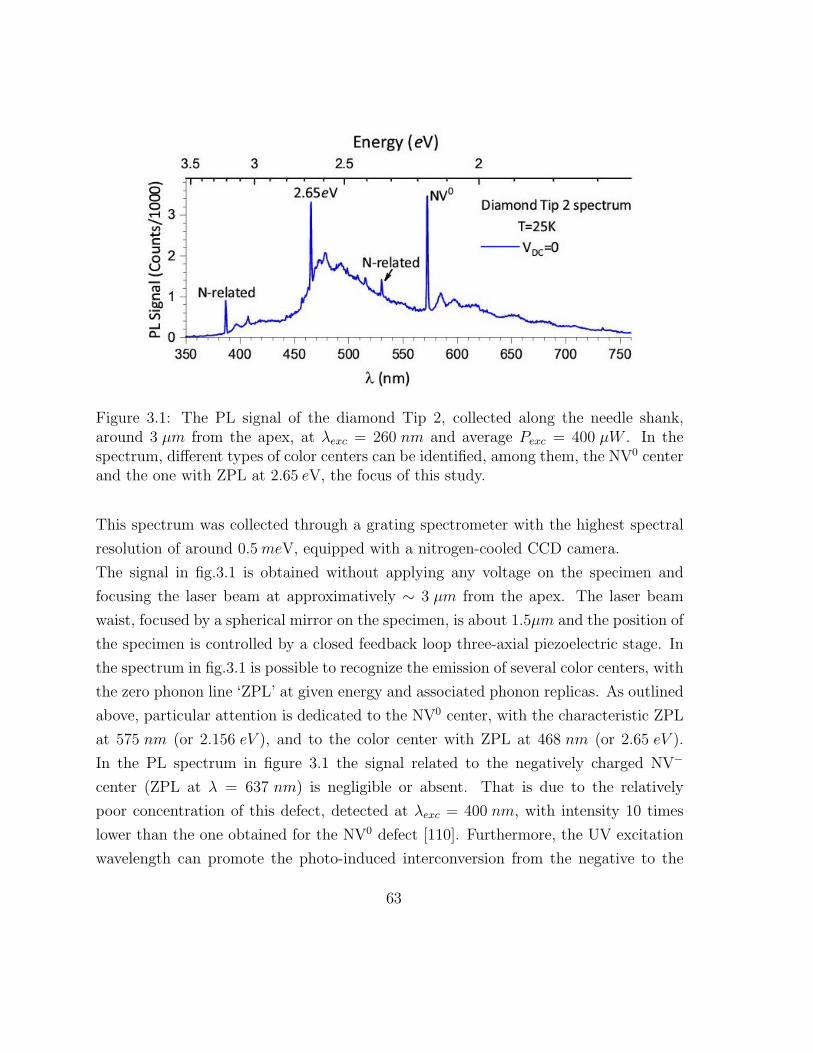
Figure 3.1: The PL signal of the diamond Tip 2, collected along the needle shank,around 3 µm from the apex, at λexc = 260 nm and average Pexc = 400 µW . In thespectrum, different types of color centers can be identified, among them, the NV0 centerand the one with ZPL at 2.65 eV, the focus of this study.
This spectrum was collected through a grating spectrometer with the highest spectral
resolution of around 0.5meV, equipped with a nitrogen-cooled CCD camera.
The signal in fig.3.1 is obtained without applying any voltage on the specimen and
focusing the laser beam at approximatively ∼ 3 µm from the apex. The laser beam
waist, focused by a spherical mirror on the specimen, is about 1.5µm and the position of
the specimen is controlled by a closed feedback loop three-axial piezoelectric stage. In
the spectrum in fig.3.1 is possible to recognize the emission of several color centers, with
the zero phonon line ‘ZPL’ at given energy and associated phonon replicas. As outlined
above, particular attention is dedicated to the NV0 center, with the characteristic ZPL
at 575 nm (or 2.156 eV ), and to the color center with ZPL at 468 nm (or 2.65 eV ).
In the PL spectrum in figure 3.1 the signal related to the negatively charged NV−
center (ZPL at λ = 637 nm) is negligible or absent. That is due to the relatively
poor concentration of this defect, detected at λexc = 400 nm, with intensity 10 times
lower than the one obtained for the NV0 defect [110]. Furthermore, the UV excitation
wavelength can promote the photo-induced interconversion from the negative to the
63
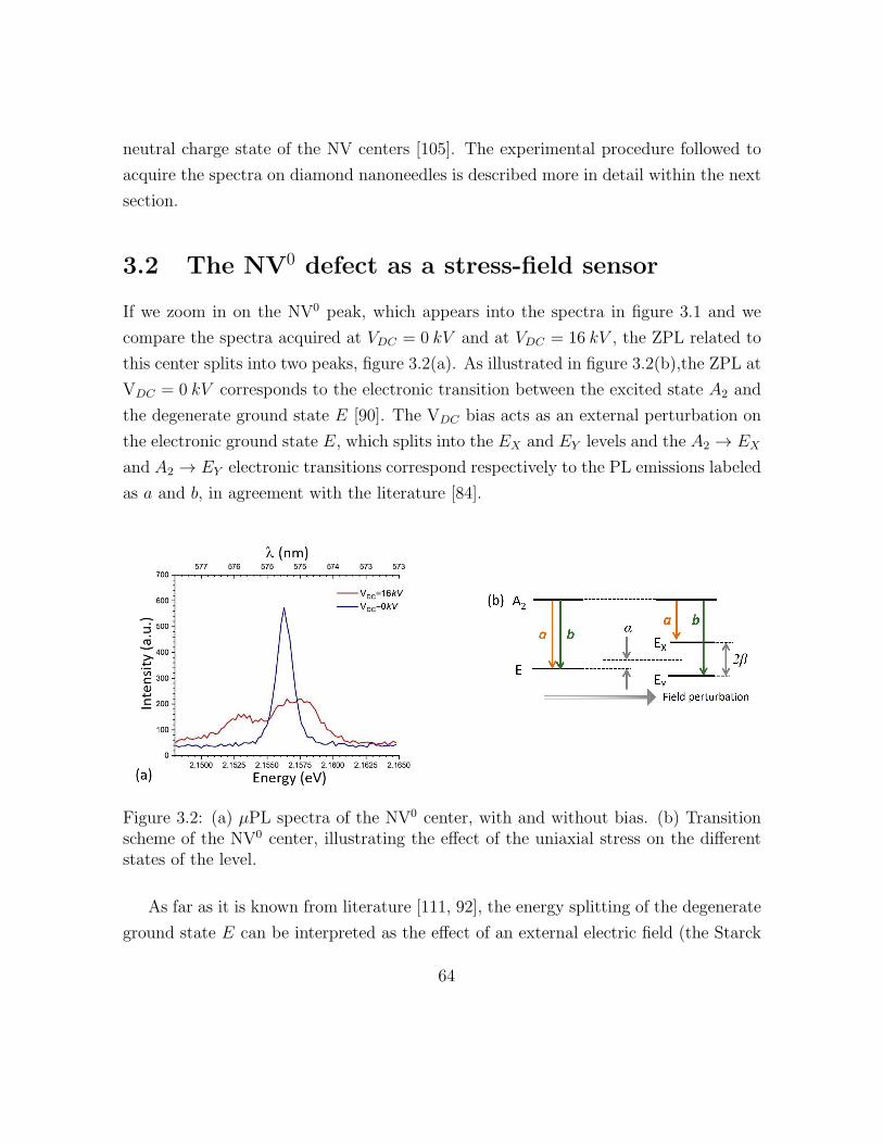
neutral charge state of the NV centers [105]. The experimental procedure followed to
acquire the spectra on diamond nanoneedles is described more in detail within the next
section.
3.2 The NV0 defect as a stress-field sensor
If we zoom in on the NV0 peak, which appears into the spectra in figure 3.1 and we
compare the spectra acquired at VDC = 0 kV and at VDC = 16 kV , the ZPL related to
this center splits into two peaks, figure 3.2(a). As illustrated in figure 3.2(b),the ZPL at
VDC = 0 kV corresponds to the electronic transition between the excited state A2 and
the degenerate ground state E [90]. The VDC bias acts as an external perturbation on
the electronic ground state E, which splits into the EX and EY levels and the A2 → EX
and A2 → EY electronic transitions correspond respectively to the PL emissions labeled
as a and b, in agreement with the literature [84].
Figure 3.2: (a) µPL spectra of the NV0 center, with and without bias. (b) Transitionscheme of the NV0 center, illustrating the effect of the uniaxial stress on the differentstates of the level.
As far as it is known from literature [111, 92], the energy splitting of the degenerate
ground state E can be interpreted as the effect of an external electric field (the Starck
64

effect) [111] or as the effect of a stress field (the Jahn-Teller effect) [92] or also a com-
bination of both. The simplest hypothesis is that the electronic levels associated to the
NV0 center shift (Stark shift), because the electric field is not perfectly screened at the
surface and it propagates inside of the sample. For the Stark effect, the relationship
between the energy splitting (∆E ) and the bias applied (or the electric field) is linear,
as it is reported in equation (3.3). In some cases, a quadratic dependence of the energy
splitting, of the NV0 electronic states, with the applied electric field was associated to
a Stark effect by P. Tamarat et al. [111].
∆E ∝ Fapplied =VDC
k ·Rapex
(3.3)
If we suppose, as predicted by E. P. Silaeva et al. [16] that the electric field is screened
at the surface of the specimen, the electronic states of the NV0 defect shift under the
action of the stress, which propagates inside the sample. In that case, following eq.(3.1)
the relationship between the energy splitting ( ∆E ) and the applied electric field is
quadratic:
∆E ∝ σ ∝ F 2applied = (
VDC
k ·Rapex
)2 (3.4)
In this case, the energy splitting is associated to the Jahn-Teller effect that the stress
induces on the ground state E, which splits into two components EX and EY , as outlined
above, fig.3.2(b). The effect of the stress on the energy transitions can be expressed
through a secular matrix acting on the basis of the EX and EY states [92]:
Vstress =
[
α + β γ
γ α− β
]
(3.5)
The terms α, β and γ which appear into the matrix (3.5) are elements which define the
general matrix of the stress tensor [92]. The relationship between the uniaxial stress
and the measured energy splitting is given by the equation (3.6), when the only non-
vanishing stress component in the crystal reference system (x, y, z ) is considered along
the z -axis, which coincides with the axis of the tip. Taking into account this constraint,
65

the energetic perturbation (3.5) is given by the matrix (3.6)
Vstress =
[
A1 + 2B 0
0 A1 − 2B
]
· σzz (3.6)
In the matrix of the equation (3.6) the elements A1 and B were determined in the
literature [92], with A1 = −0.743meV/GPa and B = −1.86meV/GPa. The equation
(3.6) can be written also in the form of the linear equation (3.7):
∆Ea,b = ca,b · σzz (3.7)
with the coefficients ca = A1+2B = −4.5meV/GPa and cb = A1−2B = 3.3meV/GPa.
Since the Jahn-Teller effect induces a larger energy splitting of the two electronic states
EX and EY than the Stark effect, in order to distinguish between the pure Jahn-Teller
effect and the superposition of this one with the Stark effect, we should be aware if the
electric field penetrates or not inside diamond nanoneedles. In order to know that, Field
Ion Microscopy ‘FIM’ experiments were performed, as reported by Lorenzo Rigutti et
al. [57]. FIM measurements demonstrate that diamond tips screen the electric field,
under a bias of several kV . In FIM the sample is biased at high voltage (10kV ) and
an imaging gas (Ne at p ∼ 10−5mbar) is introduced in the vacuum chamber. The gas
is field-ionized close to the tip surface by tunnel effect, if the field at the tip apex is
higher than the ionization field of the gas (35V/nm for Ne). Then, positive ions of Ne+
are projected on the detector and an image of the surface of the samples with atomic
resolution is obtained, as shown in figure 3.3. The temperature was kept at T = 50K
during the FIM experience. The formation of the FIM image (figure 3.3) proves that
the electric field at the surface of the tip is higher than 35 V/nm. In absence of the
screening effect, the electric field expected for the diamond tip (with ǫr = 5.7) at the
same experimental conditions (T , p and VDC) is of the order of 0.2 V/nm, which is too
low to field ionize the image gas. These experimental analyses were considered as a
good proof to conclude that the electric field does not penetrate inside of the diamond
tip, so, in the section 3.2.3, the energy splitting of the NV 0 ZPL is related only to the
stress-field effect.
66

Figure 3.3: Field Ion Microscopy image of the apex of a diamond needle. The yellowmarkers approximately indicate the position of the <001> pole.
3.2.1 Experimental results obtained on the NV0 stress-sensor:
dependency on the bias
The diamond-tip specimens, as reported in Chapter 1, section 1.4, after the fishing
step, are observed by SEM in order to get access to their geometry before the analysis.
Here we report on the experiments performed on two different diamond tips, whose
geometrical characteristics are resumed in the table 3.1.
needle apex radius base radius lengthspecimen Rapex (nm) Rbase (nm) L (µm)
Tip 1 69 1200 48
Tip 2 150 1800 40
Table 3.1: Geometrical parameters of the analyzed diamond needles [57]
During the analysis the ∼ 150 fs laser pulse of the La-APT/µ-PL system was
focused with a spherical mirror onto the diamond specimen with a beam waist of around
1.5µm. This large spot width is set in order to minimize the drift-induced variations of
the evaporation rate, while the potential bias is applied on the diamond sample. The
67

same laser beam excites radiative transitions inside the specimen and the PL signal is
collected and analyzed through a grating spectrometer, as outline in Chapter 1. The
analyses were performed with an average excitation power P = 400 µW , the excitation
wavelength at λexc = 260 nm and the frequency of νlaser = 500 kHz. The exciting
wavelength (λexc = 260nm), which corresponds to an exciting energy of Eexc ∼ 4.77eV ,
cannot promote the electronic transition from the valence band to the conduction band
of a pure diamond crystal, but it is enough to activate the emission from some impurities
and color centers present into the diamond crystal lattice. During the experiments, the
APT-detector is not used as a nanoanalysis tool, but rather as position sensor for the
laser spot. The APT analysis were not performed for two main reasons:
1. a higher electric field (>10 V/nm) is required in order to evaporate the whole
diamond specimen and, at high values of the VDC bias, electrical discharges inside
the APT experimental chamber can occur, with the risk to flash the specimen or
to damage the sensors, which are inside or are connected to the chamber;
2. the probed color centers, through the µPL system, are present not only at the
apex of the diamond nanotip, but within its volume, along all the length of the
tip. The evaporation of the diamond specimen can be even more complicated if
the sizes of the tip are too big in order to trigger the field ion evaporation.
The evaporation and the 3D APT-reconstruction of diamond nanotips containing color
centers could be an interesting goal to reach in future studies, since the nature of some of
these color centers, in diamond specimens as in other materials, likes SiC [112, 113, 114],
still need to be discovered [115].
Therefore, the APT detector was used as a sensor of the laser spot position along the
tip, because it is possible to collect a direct carbon evaporation, only when the laser
spot is positionated on the needle apex. The APT 3D virtual reconstruction of diamond
nanoneedle specimens was not carried out. The µPL signal from the NV0 ZPL acquired
with the laser impinging on or close to the apex of the needle 1 and needle 2, for different
values of the voltage applied on the sample are reported in the spectra in fig. 3.4. As
it is possible to observe, both the spectra show that the ZPL of the NV0 center splits
in two main components, labeled a and b. In the spectra related to the needle 1 further
68

2.13 2.14 2.15 2.16 2.17 2.180
1
2
3
4
5
6
7
8
a'
VDC b' ba
5 kV
7 kV
9 kV
11 kV
13 kV
15 kV
PL S
igna
l (Co
unts
/100
)
Photon Energy (eV)
16 kV
a+bTip 1, apex
(a)
582 580 578 576 574 572 570l (nm)
2.150 2.155 2.160 2.165
0
1
2
VDC=0
VDC=16kV
PL S
igna
l (co
unts
/100
0)
Photon Energy (eV)
a a+b b
577 576 575 574 573
Tip 2, shank
l (nm)
(b)
Figure 3.4: Optical study of the NV0 ZPL as a function of the applied bias.µPL signalfrom the NV0 ZPL acquired with the laser impinging on the apex of the needle 1 (a) andthe needle 2 (b) for different voltages applied to the specimen considered. The differentspectra were vertically shifted to be readable. The NV0 ZPL splits up into two maincomponents, labeled ‘a’ and ‘b’, and further components, a’ and b’, are visible at thehighest voltages, for the needle 1. The nonsplit ‘a + b’ component remains visible dueto the residual emission from the rest of the needle shank. The dash lines are guidesfor the eye.
69

components a′ and b′ are visible at highest voltages. The a′ and b′ components are
the a and b lines, associated to the NV0 electronic states, related to the centers placed
further from the position where the laser spot is focused, but they are anyway excited.
Indeed the laser spot covers a volume of ∼ 1µm × (100nm)2, when it is positionated
at the apex of the tip, an optic waveguide effect inside of the diamond nanoneedle is
expected. A residual emission of the non-split component a + b is present in all the
spectra and it is due to the emission of the NV0 color centers along the shank that are
not affected by the effect of the VDC bias. The plot in the fig. 3.5(a) reports the energy
difference of the a and b peaks position with respect to the nonsplit component a + b,
evaluated by the spectra in fig. 3.4, as a function of the bias applied. As it is possible
to observe, the trend of the energy splitting of the lines a and b varies as a quadratic
function of the bias applied VDC , in agreement with the relationship (3.7), which takes
into account only the effect induced by a stress-field on the electronic states of the NV0
center. Therefore, the energy splitting observed into the spectra (figure 3.4) allows to
determine the uniaxial stress acting along the needle axis, using the equation (3.7).
The plots in fig. 3.5 are related to the spectra reported in fig. 3.4. In fig. 3.5(b) the
dependence of the energy splitting of the a and b components on the square of the
applied voltage is reported. The spectra are collected with the laser spot focused at
a position assumed as the apex of the needle 1 and at 3µm from the apex position of
the needle 2 (through the equation (3.7)). The energy splitting allows determining the
uniaxial stress acting along the needle axis, which are reported on the right-hand side
axis, according to the parameters ca and cb defined in literature. As deduced by the
equations (3.1) and (3.2), the stress induced by the high electric field depends on the
geometry of the probed tip. A schematic of the ideal and real shape of the diamond-
needle is reported in figure 3.6. From the figure 3.6(a) it is visible that the apex of the
needle can be approximated as an hemispherical shape and the shank of the needle as a
truncated cone, as shown in fig.3.6(b). In agreement with this modelization, the stress
acting at the apex of the sample can be considered as hydrostatic, while at distances
from the apex equal to several Rapex, the resulting stress acting on the axial cross
section of the needle is considered uniaxial, with the only non-negligible component
that coincides with the needle axis. The resultant tension ~T along the needle axis is
70

Figure 3.5: Dependence of the energy splitting of the ZPL of the NV0 center (left-handside axis) of the a and b components on the voltage applied (a) and the square of thevoltage applied (b). The data were collected around the apex position of the Tip 1and around 3µm from the apex of the Tip 2. In fig.(b) on the right hand side axisthe related stress associated to the observed ebnergy splitting is evaluated, accordingto parameters reported in literature [92].
defined as (3.8):~T = πR2
apexσapexn<001> (3.8)
and it is considered constant along the cone. The data, reported in fig.3.5(b), were
collected with the laser spot focused at the apex of the diamond needle with a laser
beam waist of 1.5 µm, which means that the signal collected comes from a region lo-
calized around the first 1.5 µm below the apex of the needle. If the stress is considered
as hydrostatic only at distances from the apex equal to Rapex and uniaxial from that
position until the tip base, then the equation (3.7) can be used and considered as valid
independently on the position where the laser beam spot impinges onto the diamond
specimen.
In order to check out the C3v symmetry of the NV0 diamond centers, polarization-
resolved analysis were performed focusing the laser spot at ∼ 3 µm from the apex of
the needle 2 and applying a positive bias VDC = 16 kV . The uniaxial-stress-field acts
along the needle axis, which corresponds to the <001> crystalline direction and, as
illustrated in fig.3.6(e), the exciting laser radiation has associated the electric vector
71

572 573 574 575 576 577 5780
100
200
300
400
p po
lariz
atio
nl (nm)
aa+b
b
572 573 574 575 576 577 5780
100
200
300
400
s po
lariz
atio
n
(f)
Figure 3.6: Stress model of nanoscale needles under high electric field. The image illus-trates the generation of the hydrostatic stress at the needle apex (a) and its propagationalong the needle as uniaxial (b). Scanning Electron Microscopy image of the diamondneedle 2 (c), glued on the tungsten support; the π− and σ− directions correspond tothe notation for the PL analysis; (d) magnification on the apex radius of the needle 2.(e) Schematic of the polar direction of the electric field associated to the emitted laserradiation and (f) polarization spectra of the analysis of the NV0 ZPL acquired on theshank of the needle 2 at VDC = 16 kV .
Flaser, orientated along the same direction.
The polarization measurements were performed along different directions of the emit-
ted signal with respect to the needle axis direction (parallel to Flaser), assumed as the
reference direction. In the case labeled as π- polarization, the emitted signal is col-
lected at the parallel direction (0 with respect to the reference direction), while the
σ- polarization corresponds to the collection of the emitted signal at the perperpen-
72

dicular direction (90 with respect to the reference direction). In both configurations
(π- and σ- polarization), the ‘a’ and ‘b’ lines related to the NV0 PL signal, under the
stress-field, are visible, as shown in fig. 3.6(d). The ratio between the amplitude of the
‘a’ and ‘b’ peaks changes if we compare the spectrum collected at the π- polarization
and the spectrum collected at σ- polarization. The polar representation of the area
of the two components ‘a’ and ‘b’ of the NV0 ZPL (fig 3.7), shows, in agreement with
the literature [116], a trigonal C3v symmetry, with the intensity of the ‘b’ (‘a’) line
exhibiting a minimum (maximum) at 0 and 180, π polarization, and a maximum
(minimum) at 90, σ polarization. The intensity ratio bais equal to 0.46 in π polariza-
tion and to 3.5 in σ polarization, which is close to the literature values of 0 (π) and 3
(σ), respectively [117].
Figure 3.7: Polarization-resolved analysis of the NV0 ZPL acquired at ∼ 3µm from theapex of the Tip 2.
3.2.2 Experimental results obtained on the NV0 stress-sensor:
dependency on the position
The piezo-spectroscopic study of diamond nanoneedles was performed not only in re-
gions close to the apex of the diamond needle samples, but also at different positions
73
along the axis of the tip, in order to study the evolution of the stress along the tip and
to verify if the exposed model fits well the data experimentally collected.
The propagation of the stress along the needle shank was approximated by a 1D model
where the uniaxial stress is given by (3.9):
σzz(z) =|~T |S(z)
(3.9)
where the axial cross section of the needle S(z) is defined in the equation (3.10):
S(z) = π(Rapex +(Rbase −Rapex)z
Ltip
)2 (3.10)
all the variables which appear in the equation were defined into the table 3.1, respec-
tively for the two probed diamond needles. The equation (3.9) can be written also by
specifing the relation between the σzz(z) uniaxial stress and the σzz(0) stress at the
apex of the tip, as reported in the equation (3.11):
σzz(z) = σzz(0) ·S(0)
S(z)(3.11)
The spectra acquired at different position along the axis of the Tip 1, submitted to a
bias VDC = 16kV , fig.3.8(a), were fitted by the equation (3.9) or (3.11), in agreement
with the 1D model, as showed in the plot in fig. 3.8(b).
The energy shift of the a and b lines allowed to evaluate different values of the stress
as a function of the position along the tip. Then, the value of the stress at the apex
σzz(0) = σapex, which appears in the equation (3.11), was estimated from the fitting of
the data by the equation (3.11), taking into account the axial exstension of the laser
spot for the associated incertitude on the position where the evaluated stress could act
along the tip. For instance, for the Tip 1 that value is σapex = (7 ± 1) GPa , as it is
reported in the plot in fig.3.8(b). In figure 3.8(c) the data related to the diamond needle
2 are fitted using the equation (3.9), where the axial extension of the laser spot is the
absolute error associated to each position along the z-axis of the tip. The result of the
1D model fit yields a stress equal to σapex = (1.8± 0.3)GPa, acting at the apex of the
74
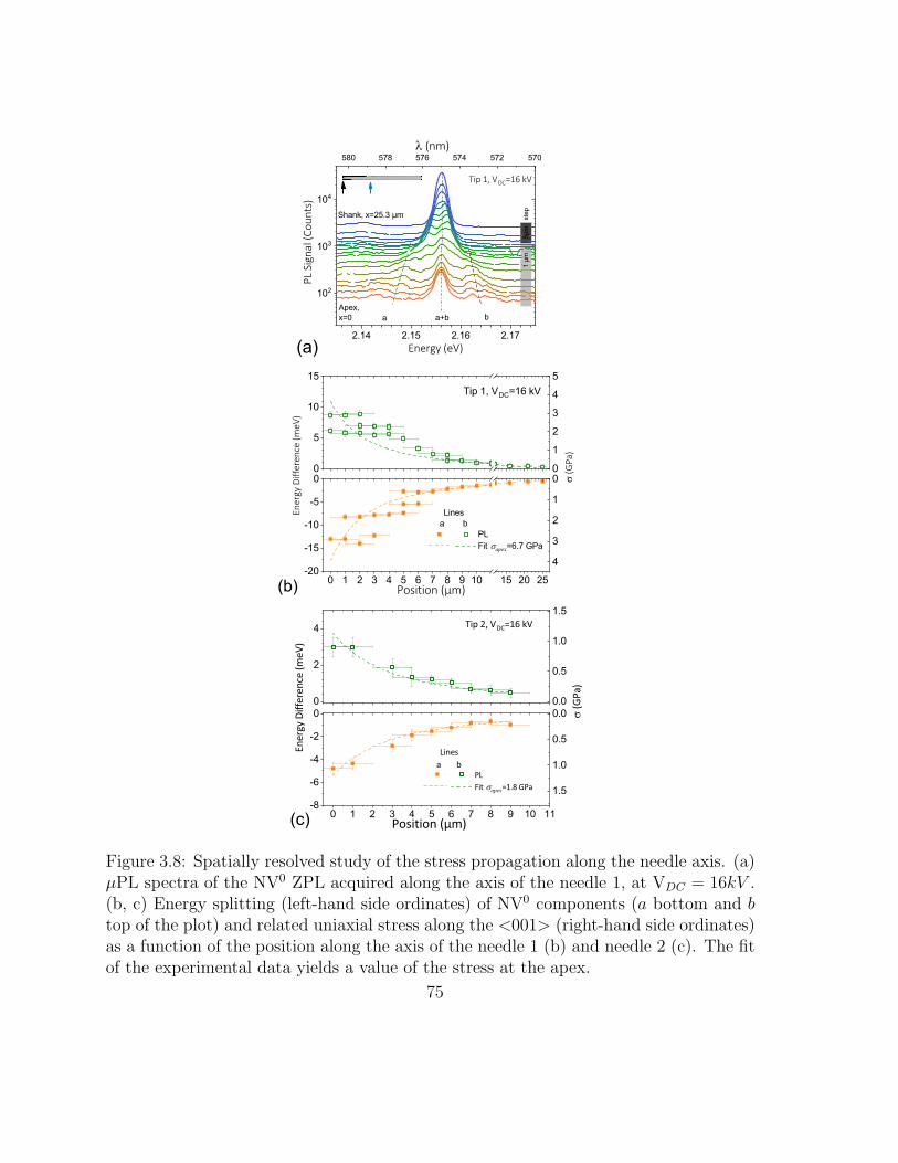
2.14 2.15 2.16 2.17
102
103
104
Shank, x=25.3 µm
ba+b
PL S
igna
l (Co
unts
)
Energy (eV)
aApex,x=0
1 µm
5µm
st
ep
Tip 1, VDC=16 kV
(a)
580 578 576 574 572 570l (nm)
0
5
10
15Tip 1, VDC=16 kV
PL Fit sapex=6.7 GPa
Linesa b
Position (µm)
Ener
gy D
iffer
ence
(meV
)
(b) 0 1 2 3 4 5 6 7 8 9 10 15 20 25-20
-15
-10
-5
0
4
3
2
1
0 s (G
Pa)
0
1
2
3
4
5
0
2
4 Tip 2, VDC=16 kV
PL Fit sapex=1.8 GPa
Linesa b
Position (µm)
Ener
gy D
iffer
ence
(meV
)
0 1 2 3 4 5 6 7 8 9 10 11-8
-6
-4
-2
0
1.5
1.0
0.5
0.0 s (G
Pa)
(c)
0.0
0.5
1.0
1.5
Figure 3.8: Spatially resolved study of the stress propagation along the needle axis. (a)µPL spectra of the NV0 ZPL acquired along the axis of the needle 1, at VDC = 16kV .(b, c) Energy splitting (left-hand side ordinates) of NV0 components (a bottom and btop of the plot) and related uniaxial stress along the <001> (right-hand side ordinates)as a function of the position along the axis of the needle 1 (b) and needle 2 (c). The fitof the experimental data yields a value of the stress at the apex.
75
diamond Tip 2. From stress acting at the apex of these two tips, the corresponding
electric field can be calculated by the equation (3.1): FS = (38±3)V/nm for the needle
1 and FS = (18 ± 2) V/nm for the needle 2. The significant difference of the value
of stress and electric field between the two diamond nanoneedles can be explained in
terms of their geometry. The first needle has a sharper apex radius than the needle
2 and as consequence, at the same values of the VDC bias applied, a higher stress is
acting on the needle 1 than on the second one.The equation (3.2) allowed to evaluate
the coefficients kf for the two needles, which are, respectively, kf = (5.0± 0.3) for the
needle 1 and kf = (6.3± 0.3) for the needle 2, which increasing value is expected as a
function of the increasing shank angle of the needle. The stress evaluated at the apex
of the Tip 1 (σapex ∼ 7 GPa) is of the same order of magnitude of typical values of
Peierls stress, reported within the articles [118, 119]. Since the Peierls stress is defined
as the force needed to move a dislocation within a plane of atoms in the unit cell,
then the magnitude of this force varies periodically as the dislocation moves inside the
plane. The probed diamond nanoneedles contain a certain concentration of defects and
not a perfect conic shape, figure 3.6(d), then shear components may develop, yielding
dislocation movements close to the apex [120]. The apex stress of 7GPa is also close to
the value of the yield strength of diamond with extended defects [121]. The diamond
needles analyzed were observed by SEM also after the analysis and they were crack-free
and did not exhibit fractures. As reported into the published article [57] about the piezo-
spectroscopic study on diamond nanoneedles, the evaluation of the stress is useful also
in order to compare our results with the values of strain reported from previous works
based on cantilever systems [122, 123, 124, 125]. The conversion between the evaluated
apex stress and the related strain comes from the Hooke’s equation: σ3 = E · ǫ3, definedin the section 2.4.1 of the Chapter 2. Considering the Young’s modulus of diamond,
E = 1050GPa, then it is possible to estimate an upper bound for the electrostatically
induced strain state of ǫzz ≈ 0.3%. In the single-crystal diamond cantilever system,
the maximum value obtained for the strain is ǫ ≈ 0.25%, which is very close to our
case. The difference between the cantilever system for the application of a mechanical
stress and the electrostatically induced stress is that in the first case, the system can
also work in compression, while in our case only in tension. Anyway, through this new
76

piezo-spectroscopic technique is possible to probably obtain higher values of the tensile
strain, using smaller tip radii, but at the same time field-evaporation will simultaneously
occur.
3.2.3 Experimental results obtained on the NV0 stress-sensor:
investigation of the radiative lifetime
The characterization of the NV0 color centers was performed also by time resolved µPL
measurements (TRPL). These kind of measurements were useful in order to study the
temporal dynamic of the recombination processes. Indeed, when the laser radiation is
absorbed by the sample, electron-hole pairs are generated between the intra-gap levels
and their quantity depends on the laser pulse power. As time passes, the number of
carrier pairs which did not recombine decrease, so, it follows that the PL intensity
signal is related to the lifetime of the radiatively recombination processes. The time
dependence of the number of excited electron-hole pairs is proportional to the intensity
of the collected PL signal. The time dependence of the PL signal can be expressed as:
I(t) = I0e− t
τ (3.12)
where: I0 is the PL intensity at t = 0 s, τ is the lifetime associated to the lumines-
cence signal of the neutral-nitrogen vacancy, with ZPL at λ = 575nm. As reported into
the section 2.5.3 of Chapter 2, the NV centers were largely studied in literature and the
value of their radiative lifetime ‘τ ’ is not affected by the temperature range at which
they are observed [126], but it depends on the structure and structural defects present
into the diamond studied (e.g. bulk [102]: τ = 20 ns, nanodiamond [99]: τ ∼ 25 ns,
for the single-crystal diamond needles [88]: τ = ( 2.8 ± 0.3 ) ns and Hanzawa et al.
[126] found two different values of decay time associated to the NV0 center: τ = 2 ns
and τ ∼ 9 ns, respectively for the short and long component of the decay curve, for
synthetic Ib diamond samples).
The fig.3.9(a) shows the 2D colormaps which were recorded by streak camera (at
P = (5.0± 0.5)mW, λexc = (260± 5) nm and T = 25K). The 2D datasets, related to
77

0 50 100 150 2000
1
2
3
4
5
6
(b)
ln(I
nten
sity)
(a.u
.)
Time (ns)
ln(Intensity NV 0) Linear fit Dt=[0;42]ns
t= (34.6±8.1)ns
Equation y = a + b*x
Plot ln(I)Weight No WeightingIntercept 5.93432 ± 0.02616Slope -0.03656 ± 0.00508Residual Sum of Squares 0.06994Pearson's r -0.84951R-Square (COD) 0.72166Adj. R-Square 0.70775
Equation y = a + b*x
Plot ln(I)Weight No WeightingIntercept 4.60225 ± 0.07675Slope (-1/ ) -0.02893 ± 0.00287Residual Sum of Squares 19.70923Pearson's r -0.68539R-Square (COD) 0.46976Adj. R-Square 0.46515
0 50 100 150 200
0
1
2
3
4
5
6
(d)
ln(I
nten
sity)
(a.u
.)
Time (ns)
ln(Intensity NV 0) Linear fit Dt=[0;36]ns
t= (15.0±3.0)ns
Equation y = a + b*x
Plot ln(I)Weight No WeightingIntercept 5.60527 ± 0.07934Slope (-1/ ) -0.06661 ± 0.00382Residual Sum of Squares 14.83992Pearson's r -0.87516R-Square (COD) 0.76591Adj. R-Square 0.76339
Figure 3.9: Time distribution of events of the 575nm line (NV0 center), detected atT=25 K, λexc = 260 nm, beam power of Pexc = ( 5.0± 0.5 )mW , focusing the laser onthe same position (at the apex of the diamond tip). The 2D colormap (a) was obtainedwithout applying any bias. While the 2D colormap (c) was acquired at VDC = 16 kV .In both, (a)-(c), 2D colormaps the brown color is associated to the lowest number ofdetected events and the white color to the highest ones. The (b)-(d) integrated spectraof the events, over the energy ranges of the NV0 peak: [ 574; 576 ] nm, are related,respectively, to the color maps (a) and (c). Integration time ranges are indicated,in (a)-(c), on the streak detection map with bars of the corresponding colors. Theacquisition time of the data collected at VDC = 0 kV , (a)-(b), is 1 hour, while theacquisition time of the data collected at VDC = 16kV , (c)-(d), is 12 hours. Red dashedlines correspond to exponential decay adonlyment in linear scale (b)-(d).
the figures 3.9(a) and (c), were integrated over the restricted wavelength range ∆λ =
[ 574; 576 ] nm, in order to obtain the related decay curves, as shown in figures 3.9(b)
78

and (d). The decay curve is characterized by a single peak with a really short rise-time
(comparable with the time resolution of the streak-camera of ∆t ∼ (6.0± 1.2) ns) and
longer decreasing tail. The radiative lifetime is experimentally determined by fitting the
decay curves with decay models, equation (3.12). The 2D colormap in fig. 3.9(a) was
acquired without applying any bias, VDC = 0kV , focusing the laser spot (dspot ≈ 1.5µm)
on the apex of the diamond needle 2 and the acquisition time was one hour. For the
2D colormap in fig. 3.9(c), the position of the laser spot was not changed, but a bias
equal to VDC = 16 kV was applied and the acquisition time of the measurement was
12 hours. Despite the increasing of the acquisition time, the measurements, of both 2D
colormaps, show low signal/noise ratio, which is clearly visible from the related decay
curves fig. 3.9(b) and (d). This low signal/noise ratio, shown in fig. 3.9, is supposed to
be related to the low amplitude of the NV 0 PL-signal, when the laser spot impinges on
the apex of the diamond tip. The decay time, evaluated by the decay curve in fig. 3.9(b),
without applying any bias, is τ = (34.6 ± 8.1) ns, with an incertitude of ∼ 24%, due
to the low signal/noise ratio. The spectra in fig. 3.9(d), obtained by the 2D colormap
in fig. 3.9(c), shows a better quality of the signal/noise ratio. The NV0 decay time is
evaluated to be: τ = (15.0± 3.0) ns, with an incertitude of ∼ 20%. Unfortunately, we
have only one result related to the decay time, evaluated respectively with and without
applying any bias, close to the apex position. The different values of the decay time
obtained at VDC = 0 kV ( τ = (34.6± 8.1) ns) and VDC = 16 kV (τ = (15.0± 3.5) ns),
suggest that the high bias affects also the lifetime associated to the NV0 radiative
emission, as it is expected by a changement of the geometry of the diamond tip or the
relative distance between the atoms due to a strain/stress effect acting on the diamond
needle (at VDC = 16 kV ). But the results obtained cannot be considered conclusive.
Another measurement at VDC = 16 kV was performed in short time scale (5 ns),
along the shank of the tip. The decay curve is reported in fig. 3.10(a) and the related
acquisition time is around ≈ 2 hours.
The characteristic decay time of the NV0 decay curve in fig. 3.10(a) was found to
be τ = (1.34 ± 0.42) ns. That value, obtained through the linear fit, equation (3.12),
indicates that in short range time a fast decay time seems to occur, in agreement with
what reported by Malykhin et al. [88]. The NV0 decay curves acquired without bias,
79

Figure 3.10: Time dependences of the photoluminescent 575nm line (NV0) decay on(a) short and (b) long time scale. Excitation wavelength is λexc = 260 nm and andthe beam power is Pexc = (5.0± 0.5)mW . Red dashed lines correspond to exponentialdecay adonlyment in semi-logaritmic scale (a) and (b).
on long time scale (200ns), at three different positions along the diamond needle shank
are reported in fig.3.10(b) and each signal was acquired in a range of time of ≈ 2hours.
The three different positions are disposed in increasing order, moving from the apex
towards the base of the diamond tip and the related decay times are:
- position 1: τ1 = (29.9± 3.0) ns
- position 2: τ2 = (26.6± 3.2) ns
- position 3: τ3 = (22.4± 2.6) ns
These results show that the decay time of the NV0 centers evolves along the diamond
tip and it seems to decrease as the diameter of the diamond tip becomes larger. The av-
erage value of the decay time acquired at these different positions is τ = (26.3±5.0 )ns
is in quite good agreement with the decay time previously reported in literature:
τ = (29.41 ± 6.98) ns [99] and τ = (28 ± 1) ns [110], for nanodiamond samples. The
decay time ‘τ1 = (29.9± 3.0) ns’ at the position 1, the closer to the diamond tip apex,
is also comparable with the value ‘τ = (34.6± 8.1) ns’ calculated from the decay curve
in fig.3.9(b).
80

In ref.[88], fluorescent lifetime imaging spectroscopy ‘FLIM’ was used in order to eval-
uate the decay time related to different color centers present into the same kind of
diamond tip specimens. In this article [88] it is reported that a decrease in size of the
diamond crystal corresponds to an increment in lifetime, in the long time range scale,
of the NV centers. So, the lifetime of the NV centers in a diamond needle is expected
to decrease from its apex towards its base. Since the internal structure is quite similar
over the length of the diamond tips, the only explanation for this variation of the char-
acteristic decay times, in particular for the NV0 and SiV centers, was associated to the
reduction of the crystallite thickness of diamond needles. In ref.[99], cited in the section
2.5.3 of Chapter 2, is reported that “in agreement with local density of states (LDOS)
theory, as the crystal size becomes smaller, an increase of the NV0 lifetime is expected
and as the size of nanodiamond decrease, a decrease of the lifetime, which could might
be related to a preferential coupling to non-radiative pathways, is expected”.
For what concerns the study of the bias on the radiative lifetime of the NV0 centers,
we can conclude that this study gives some clues to think that the stress induced by
the high bias decreases the decay time of these color centers, but further experimental
proofs are required.
3.3 The color-center at 2.65eV
The piezo-spectroscopic study performed on the NV0 center was achieved using the cou-
pled La-APT/µPL setup as an original optical contactless-piezo-spectroscopic system.
Thanks to this new technique the stress-field sensitivity of the nitrogen-vacancy
‘NV0’ center was compared with the one of the color center detected with ZPL at
468nm or 2.65 eV in the wide-spectrum in fig.3.11. The reasons why it was decided to
study this color center can be classified in this order:
1. Looking at the whole spectrum at VDC=0kV, in fig.3.11, the ZPL of the center
at 2.65 eV has almost the same intensity as the NV0 center, so the 2.65 eV and
the NV0 have both a good PL signal at the exciting wavelength, λexc = 260nm,
81

Figure 3.11: PL signal of the diamond Tip 2, at the experimental conditions reportedin caption of fig.3.1. The blue spectrum was acquired without bias, while the red oneat VDC=16kV and in both the spectra the focus is on the signal of the 2.65 eV centerand the NV0.
selected to perform the analysis.
2. The PL signal of the center at 2.65 eV is visibly affected by the applied VDC bias,
as it is shown in the spectra in fig.3.11.
3. The potential of the center at 2.65 eV as a stress-sensor was never tested and also
the structure and symmetry of this center are not well known in literature[6, 116,
4].
As demonstrated in ref. [57], the NV0 optical transition can be controlled by a stress/strain
field and this kind of study opens the way to the realization of strain-coupled hybrid
spin oscillator systems, where the NV center spins interact with the resonant phonon
modes of a macro-mechanical resonator through crystal strain. Some applications of
these systems are reported in the articles[122, 123], where the NV centers were choosen
for their ability to couple to external strain fields. In figure 3.11, at VDC = 0 kV, the
NV0 peak and the one with ZPL at 2.65 eV have comparable amplitudes, while, under
the bias VDC = 16 kV, the intensity of the 2.65 eV center decreases more than the
82

intensity of the NV0 center. This trend suggests that the 2.65 eV color center could
be also more sensitive to the stress-field than the NV0 defect. In order to observe and
compare the energy splitting of the peaks, as it was done for the NV0 defect, a re-
stricted region of the spectra, centerd on the value of the ZPL of the interested defect,
is acquired with a grating density of 1200groove/mm and λblaze = 400nm. That choice
allows to increase the spectral resolution since 0.5meV, which allows to appreciate the
expected energy shift of the peaks, of the order of some meV for the NV0 defect. Be-
fore to move to the experimental analysis related to the 2.65 eV center, it is worth to
point out that the nature of this color center was largely discussed in literature[107].
For instance, in agreement with the energy range were this defect can be detected
EZPL = [ 2.648; 2.654 ] eV, it was supposed that it corresponds to the TR12’ diamond
defect. The TR12’ is called like that, because its ZPL is 10meV blue- shifted with re-
spect to the TR12 color center [127, 5]. The 2.65eV center was observed on most of the
as-grown chemical vapor deposition (CVD) diamond films studied by Iakoubovskii et
al.[5]. Unlike the TR12 center, which anneals out at 800C, the intensity of the 2.65 eV
center was almost constant in CVD diamond films grown annealed up to 1000C[6]. The
potential of the 2.65 eV center as a stress-field sensor was never tested before[4, 6, 128],
but the TR12 center was observed in the PL spectrum of diamond decades ago, by
Davies et al.[4], and piezo-spectroscopic studies were performed on it, in order to de-
termine the strain susceptibility and the symmetry of this center. The measured strain
susceptibility (sensitivity) of this center is lower than the one of the NV0 center and the
corresponding symmetry was not established[4]. Concerning the structure of the TR12
center Mainwood et al.[129], suggested that this center contains an interstitial carbon
in a hexagonal site. Recently, Naydenov et al.[130] have demonstrated the ability of
the TR12 center as single photon emitter, fueling interest about this color center and
the related TR12’ or the 2.65 eV center. About the TR12’ center, Iakoubovskii et al.[5]
suggested that it is a stressed TR12 center, with the stress generated through the lattice
or some neighboring impurity, but the symmetry of this center is still not well known.
In the next section, the contactless piezo-spectroscopy of the 2.65 eV center is used to
prove that this color center could be a better candidate than the NV0 center for the
fabrication of strain-mediated coupling systems. Thanks to polarization-resolved µ-PL
83

measurements, under strain field, more information about the symmetry and structure
of the 2.65 eV center was obtained.
3.3.1 Piezo-spectroscopic study of the center at 2.65eV : de-
pendence on the VDC bias
Contactless piezo-spectroscopy studies were performed on three diamond specimens,
synthesized by PE-CVD technique, as explained into section 2.5.1 of Chapter 2. The
exact geometry of two of these samples was measured by scanning electron microscopy
(SEM) and in the table 3.2, the geometrical characteristics of these two diamond spec-
imens are reported.
needle apex radius base radius lengthspecimen Rapex (nm) Rbase (nm) L (µm)
Tip 2 150 1800 40
Tip 3 71 500 21
Table 3.2: Geometrical parameters of the analyzed diamond needles [115]. The Tip 2is the same specimen used for the piezo-spectropic analysis of the NV0 center.
The SEM images of these two samples are reported in figure 3.12.
The experiments were performed at the same conditions reported for standard APT
analysis: T < 25K and p < 10−7Pa, applying a tuning positive bias VDC = [0; 16 ]kV ,
and as for the NV0 centers, using an excitation wavelength of λ = 260 nm and average
power of P = 400 µW . Also in that case, an incertitude of 1.5 µm has to be associated
to the laser position on the tip, which corresponds to the waist of the laser beam, when
it is focused on the diamond needle specimen during the analysis. In particular, a series
of PL spectra was acquired for the 2.65 eV center and the NV0 center with the laser
spot focused on the apex of the needle 3, for different values of applied bias, from 0 kV
to 16kV , as reported in figure 3.13(a) and (b). The spectra of the NV0 center are shown
for comparison and as reference for the evaluation of the stress acting at the apex of
the diamond needle, labeled ‘Tip 3’.
84

Figure 3.12: SEM images of the diamond nanoneedles: (a) the Tip 3, acquired withat magnification scale of 1 µm and (b) the Tip 2, acquired at a magnification scale of10 µm
The spectra of both the supposed TR12’ center and the NV0 center, at low bias, consist,
within 1 meV of spectral resolution limit of the setup, of single emission peaked at
EZPL = 2.65 eV and EZPL = 2.15 6eV respectively. At higher biases (VDC > 8 kV),
the line splits up into two components, denoted as ‘a’ and ‘b’, which shift: ‘a’ towards
lower energy and ‘b’ towards higher energy, as the bias is increased.
As explained in the section 3.2, the ‘a’ and ‘b’ lines which appears in the spectra of
the NV0 center (fig.3.13(a)) correspond to two different electronic transitions activated
by the effect of the stress-field on the E ground state level of the NV0 center. In
analogy, the ‘a’ and ‘b’ lines, which appear in fig.3.13(b), can be associated to electronic
transitions activated for the 2.65eV center under the effect of the stress field. Differently
from the NV0, where the ‘a’ and ‘b’ lines have almost the same amplitude (fig.3.13(a)),
in the 2.65 eV center, the ‘a’ line has lower amplitude than the ‘b’ line, as visible in
fig.3.13(b). Moreover, at high biases, a new b’ line is visible, but none a’ line is observed,
probably because of its lower intensity, that it is covered by the noise level. The b and b’
lines are attributed to two different centers, simultaneously excited by the laser beam,
but subjected to a different perturbing stress-field, probably because they are placed at
different positions inside the tip. The relationship between the energy splitting of the
85

572 573 574 575 576 577 5780.0
0.2
0.4
0.6
0.8
1.0
1.2
1.4
1.6
1.8
Inte
nsity
(Cou
nts/
1000
)
l (nm)
VDC=0kV
VDC=4kV
VDC=6kV
VDC=8kV
VDC=10kV
VDC=11kV
VDC=12kV
VDC=13kV
VDC=13.5kV
VDC=14kV
VDC=15kV
(a)
b a
2.17 2.16 2.15 2.14Energy (eV)
464 466 468 470
2.67177 2.6603 2.64893 2.63766
0.0
0.5
1.0
1.5
2.0
2.5
3.0
3.5
4.0
4.5
5.0
5.5
6.0
Energy (eV)
VDC=0kV
VDC=4kV
VDC=6kV
VDC=8kV
VDC=10kV
VDC=11kV
VDC=12kV
VDC=13kV
VDC=14kV
VDC=15kV
VDC=16kVInte
nsity
(Cou
nts/
1000
)
l (nm) (b)
b' b a
0 50 100 150 200 2500
1
2
3
4
5
6 line b of the 2.65eV centre line b of the NV0 centre
0 50 100 150 200 250
-6
-5
-4
-3
-2
-1
0
line a of the 2.65eV centre line a of the NV0 centre
V2DC (kV2)
Ener
gy d
iffer
ence
(meV
)
(c)0.0 0.1 0.2 0.3 0.4 0.5 0.6 0.7
-6
-5
-4
-3
-2
-1
line a
s (GPa)
Ener
gy d
iffer
ence
(meV
)
(d)
0.0 0.1 0.2 0.3 0.4 0.5 0.6 0.70
1
2
3
4
5
6 line b
Figure 3.13: µ-PL signal acquired with the laser impinging on the apex of the diamondTip 3, at different values of applied VDC . The spectra related to the NV0 ZPL (a) andto the ZPL of the 2.65 eV center (b), which are vertically shifted for clarity. The ZPLat 0 kV , when the bias is increased, splits up into two main components ‘a’ and ‘b’ andthe dashed lines are guides to the eye. (c) Dependence of the energy splitting of the‘a’ and ‘b’ components on the square of the applied voltage, related to the spectra (a)and (b). (d) Dependence of the energy splitting of the ‘a’ and ‘b’ components of the2.65 eV center with the stress along the needle axis <001> (crystal orientation).
86

‘a’ and ‘b’ lines is a quadratic function of the applied bias, as reported in the equation
(3.7) and it is shown in figure 3.13(c). The uniaxial stress, acting on the diamond Tip 3,
is evaluated by the equation (3.7), where the value of the NV0 coefficients are taken by
ref.[92] and the energy difference corresponds to the split positions of the peaks reported
in the spectra in fig.3.13(a). The ∆Ea,b related to the NV0 center can be used in order
to calibrate the tensile stress at a fixed z position, as a function of the applied bias.
The evaluated uniaxial tensile stress at z ≈ 0µm, as reported in fig. 3.13(d), was found
to vary in the range: σaverage = [ 0; 0.6 ] GPa with the variation of VDC = [0; 14] kV.
Also for the 2.65 eV center the trend observed between the energy splitting, ∆Ea,b, of
the ‘a’ and ‘b’ lines as a function of the average value of the applied stress, σaverage,
is linear, in agreement with the equation (3.7). That equation can be written for the
2.65 eV center, as:
∆Ea,b = ka,b · σzz (3.13)
Where the coefficients of proportionality in the equation (3.13) are obtained by the linear
fit of the data reported into fig.3.13(d). Their values: ka = −(10.7 ± 0.3) meV/GPa
and kb = (10.0± 0.3)meV/GPa are larger than the values of the ca,b NV0 coefficients,
by more than a factor 2. But, as discussed for the NV0 analysis, the large laser beam
waist does not exclude systematic errors related to the excitation of other color centers
close to the apex position. A different position of the NV0 or 2.65 eV centers can
translate in a significant different stress state acting on one or the other. For this
reason, spatially-resolved PL measurements were performed on Tip 2.
3.3.2 Piezo-spectroscopic study of the center at 2.65eV : de-
pendence on the position
In parallel to what was done for the NV0 center, the PL spectra of the 2.65 eV color
center were acquired at different positions of the laser spot with respect to the apex of
the Tip 2, applying a constant bias VDC = 16kV. When the laser is focused close to the
apex of the needle, the ZPL of the 2.65 eV center splits up into different components,
similarly to what shown into fig.3.13(b) and as showed into fig.3.8(a) for the NV0 center.
The energy splitting of the ‘a’ and ‘b’ lines for the two centers is plotted as a function
87

of the laser spot position with respect to the apex of the needle in figure 3.14.
0 1 2 3 4 5 6 7 8 9-10
-9-8-7-6-5-4-3-2-10
Line a
Position (mm)
0 1 2 3 4 5 6 7 8 90123456789
10
b of the 2.65eV centre of the NV 0 centre
Ener
gy D
iffer
ence
(meV
)
Figure 3.14: Evolution of the energy splitting related to the ‘a’ and ‘b’ lines related thethe 2.65 eV and the NV0 centers as a function of the position along the axis of the tip(<001> crystal direction).
Looking at the data reported into the plot in figure 3.14, the ∆Ea,b of the NV0 color
center is higher than 1meV up to 4 µm from the apex, but it progressively decreases
to zero. The behavior of the 2.65 eV center is similar to that of the NV0 center,
but the spectral shift is higher than 2 meV up to the furthest position of 10 µm. As
discussed above, in section 3.2.2, and proved in ref. [57], the value of the uniaxial stress,
at the coordinate z, for a circular cone geometry, depends strictly on the geometrical
parameters of the tip (Rapex, Rbase and Ltip), in agreement with the equation in the
equation (3.10). For what concerns the Tip 2, the value of the stress acting at its apex:
σapex = (1.8±0.3)GPa [57] was evaluated from the fit of the experimental data, related
to the NV0 center, reported in fig. 3.8(c), through the equation (3.10). Therefore, using
the equation (3.13), the value of the two coefficients, related to the 2.65 eV center,
are evaluated: ka = −(11 ± 1) meV/GPa and kb = (10.0 ± 0.5) meV/GPa. These
values of the coefficients ka and kb, on the Tip 2, are in good agreement with the values
obtained on the diamond Tip 3, so they can be considered as a new result related to the
88

2.65 eV center, since the value of these coefficients was evaluated with two independent
methods. From the equations (3.7) and (3.13) it follows that the ‘ca’ and ‘cb’ or the
‘ka’ and ‘kb’ coefficiens are related to the dipole moment associated to the NV0 and the
2.65 eV center, so the 2.65 eV center has an average dipole moment around two times
larger than the NV0 defect.
3.3.3 Polarization spectroscopic study of the center at 2.65 eV
under VDC bias
In order to get more information on the symmetry of the 2.65 eV center, polarization-
resolved PL spectroscopy was performed on the diamond Tip 3, while it was subjected
to a bias of VDC = 16 kV. For what concerns the polarization study of the NV0 center,
the polar representation of the area of the two components ‘a’ and ‘b’ of its ZPL
(fig.3.15(a)) confirms the trigonal C3v symmetry of this center, in agreement with the
literature [116].
-15
0
15
30
45
607590105
120
135
150
165
180
195
0.2
0.4
0.6
0.8
1.0
0.2
0.4
0.6
0.8
1.0
Perc
enta
ge a
rea
peak
s (%
)
Area peak b of NV0 center Area peak a of NV0 center
(a)
-15
0
15
30
45
607590105
120
135
150
165
180
195
0.0
0.2
0.4
0.6
0.8
1.0
0.0
0.2
0.4
0.6
0.8
1.0
Perc
enta
ge a
rea
peak
s (%
)
Area peak a (´5) of center at 468nm Area peak b of center at 468nm
(b)
Figure 3.15: Polarization-resolved analysis of the NV0 ZPL (a) and the 2.65 eV center(b) acquired on the the apex of the diamond Tip 3.
In the case of the 2.65 eV center, the ‘b’ line follows the same polarization behavior
of the ‘b’ line of the NV0 center, but, in agreement with what observed in figure 3.13(b),
its intensity is higher than the intensity of the ‘a’ line almost of a factor 10. The ‘a’
line of the 2.65 eV center shows an increase in intensity of about 10% in π-polarization,
89

compared to the σ-polarization. Also, even though the polar behavior of the ‘a’ and ‘b’
lines of the 2.65 eV center are similar to the split components of the NV0, the intensity
ratio bais 3 in π-polarization and 10 in σ-polarization, which is incompatible with the
monoclinic I or the triclinic symmetry, suggested in literature for the TR12 and TR12’
centers[117, 6, 4, 128].
In summary, the piezo-spectroscopic measurements performed on the 2.65 eV centers,
which are present into needle-shaped diamond crystal, with nanometric apex radius and
the axis oriented along the <001> crystal direction, allowed to conclude that:
1. the splitting of the 2.65 eV center is twice as large that of the NV0 center. This
result was confirmed by two different methodologies in order to vary the uniaxial
tensile stress and on two different samples.
2. the symmetry found out for the 2.65 eV center, along the <001> direction, does
not confirm the monoclinic I and also not the trigonal one. In order to determine
the symmetry, piezo-spectroscopy should be performed applying uniaxial stress
along different crystal directions.
3. since the 2.65 eV color center is largely present into the needle-shaped nanoscale
diamond tips, it can be a valid alternative to the NV-centers in the framework of
nanoscale probes of electromagnetic fields.
The study about the 2.65 eV color center was recently published in the article[115].
3.4 Multi-photon excitation of the NV0 defect into
the IR range
The multi-photon absorption (MPA) is a process that can occur in band-gap materials
only if the energy of two or more absorbed photons (n · hν) is higher than the energy
gap (∆E > Egap) or equal to the intragap electronic transitions (∆E = Ee − Eg) of
the probed material. Ee and Eg label the energy of the excited electronic state and the
energy of the ground electronic state, respectively, as reported in fig. 3.16.
90

In order to promote an electronic transition through a two- or multi-photon absorption,
the photons have to be absorbed within a range of time given by the Heisenberg lifetime:
(∆t = h∆E
), which is of the order of a few fs for ∆E corresponding to the visible light
spectral range.
Figure 3.16: Schematic of the multi-photon transition.
Considering the easier case: two-photon absorption (TPA) causes transmission of
light through a medium to be power dependent. The simultaneous absorption of two
photons is a non-linear process that takes place with significant rates only at high
optical intensity. For a single photon absorption, linear process, the absorbed intensity
is directly proportional to the incident intensity:
Iabs = α · Iinc (3.14)
with ‘α’ as linear coefficient of proportionality. While, for a two-photons process, the
relationship between the absorbed intensity and the incident intensity is given by the
equation (3.15):
Iabs = α · Iinc + χ(2) · I2inc = (α + χ(2) · Iinc) · Iinc (3.15)
The term (α + χ(2) · Iinc), which appears in the equation (3.15), can be re-defined, in
analogy to the equation (3.14), as α’. TPA is more probable if the photon energy hν is
between: 12∆E < hν < ∆E and in general for MPA the condition is expressed as in
91

(3.16):1
n∆E < hν < ∆E (3.16)
where n is an integer that indicates the number of photons involved in the process.
Differently from the TPA, where the relation between the absorption coefficient is lin-
early dependent to the optical intensity (equation (3.14)), for MPA the absorption
coeffient is proportional to the (n−1)th power of the optical intensity, while the absorp-
tion rate is proportional to the nth power of the optical intensity. It follows that the
absorption rate is small at low or moderate optical intensity, but it becomes dominant
for very high optical intensity.
The MP excitation of NV centers was recently demonstrated to be possible in the IR-
range of wavelength by Peng Ji et al. [131]. This process of excitation of NV color
centers is extremely advantageous for biological imaging, but also for quantum infor-
matic processing, since the fluorescence signal is widely separated by the excitation
one. In ref.[131] is showed how the number of photons involved in the MP transition
associated to the NV0 centers, under high value of power, depends on the selected
near-IR excitation wavelength. In ref.[131], three excitation wavelengths were selected,
λ1 = 535 nm, λ2 = 1060 nm and λ3 = 1210 nm, and for each selected wavelength
a plot of the fluorescence emission intensity of the NV centers as a function of the
power applied is reported. In particular, for the NV0 center, 1, 2 and 3 photons are
involved in the excitation process at λ1, λ2 and λ3, wavelength, respectively. In my
study I used a 1038 nm excitation wavelength and the laser power ranged between few
mW up to hundreds of mW , in order to observe the expected two photon transition
by the NV0 centers. Furthermore, piezo-spectroscopic study was performed using IR
excitation. Since the IR light can penetrate deeply into biological tissues with little
scattering or damage [132], this study could be helpful to demonstrate the application
of nanodiamonds for biological sensors of local stress.
3.4.1 Experimental results
The IR-PL spectroscopy and the piezo-spectroscopy were performed at the excitation
wavelength of 1038 nm. The same fs-laser system, which was described in section
92

1.3 of the Chapter 1, has been used for these studies. The IR-excitation wavelength
(λexc = 1038 nm) is not enough in order to promote the electronic transition between
the ground and excited state of the NV0 defect with a single photon absorption, but this
electronic transition can occur with the absorption of two or more photons. As already
said, the MPA is a phenomenon which requires specific constraints and high power in
order to occur. By applying high intensity fs-laser on nanodiamond samples, another
non-linear effect can be induced in these samples: the generation of a super-continuum
(SC) spectra. More details about this phenomenon are reported in ref.[133].
The probed diamond nanoneedle (Tip 4) was glued to the tungsten support tip by the
FIB technique, using Pt deposition, as mentionated in the section 2.5.2 of Chapter 2.
400 500 600 7000
500
1000
1500
2000
2500
3000
Inte
nsity
(a.u
.)
l (nm)
P=213mW; x=6mm; P=300mW; x=6mm;
2.65eV
NV0
3.188eV N+
(b)
SHG2.75eV
2.298eV
3.6 3.4 3.2 3 2.8 2.6 2.4 2.2 2 1.8 1.6Energy (eV)
Figure 3.17: (a) Scanning electron microscopy image of the diamond (Tip 4), glued tothe tungsten support tip by field ion microscopy technique. (b) The PL signals obtainedon Tip 4, excited with the 1038nm fs-laser at different values of laser power. The colorcenters at :389 nm, 468 nm and 575 nm are MP excited.
A SEM image of the analyzed diamond needle is reported in fig.3.17(a). The PL
specta, fig.3.17(b), are acquired at laser excitation power Pexc > 200 mW. The MP
excitation activates the electronic transition of three different color centers, that have
already been detected in the PL wide spectrum acquired with the 260 nm laser. The
93

two peaks at 468nm and 575nm are respectively the 2.65 eV color center and the NV0
center, while the signal peaked at ∼ 519nm is the second harmonic generated (SHG) by
the IR-laser wavelength (1038nm). The color center peaked at 389 nm or 3.188 eV is a
nitrogen (N+) related center, which is well known in literature [77] and the two signals
which appear peaked respectively at 450nm or 2.75eV and at ∼ 540nm or 2.298eV are
peaks that are possibly related to some nitrogen-containing synthetic diamonds grown
in the presence of Si and Ni, as reported in ref. [77].
In the next paragraphs, we focus mainly on the IR-analyses on the NV0 center. The
results are separated in three parts:
1. Dependency of the amplitude of the NV0 on the illuminated position;
2. Piezo-spectroscopic study of the NV0 center as a function of the VDC applied bias;
3. Dependency of the amplitude of the NV0 signal on the applied power.
3.4.1.1 Dependency of the NV0 amplitude on the illumination position
As saw in section 3.2.2 of this Chapter, in order to study the effect of the VDC bias in the
PL spectra related to the NV0 centers, the laser has to illuminate a region close to the
apex of the diamond nanoneedle. Therefore, before to perform the piezo-spectroscopic
analysis, at 1038nm wavelength excitation, the study of the evolution of the amplitude
of the NV0 peak, as a function of the illumination position, was performed applying a
fixed laser power of 450mW. Each spectrum, in figure 3.18(a), was acquired at a different
value of z that corresponds to the position where the impinging laser is focused with
respect to the position of the tip apex: z = 0 µm. The negative values of z are related
to positions along the shank of the tip, while the positive ones are related to positions
outside the diamond needle. As reported in the plot in fig.3.18(b), the amplitude of the
NV0 center depends on the probed volume of the diamond tip, since it increases with
the increasing of the probed volume. The two points at - 7.7 µm and - 6.6 µm show
saturation effects, as visible in the spectra in figure 3.18(a). Since the impinging power
was really high, the acquisition time of the spectra was kept below ∆tacquistion < 10 s,
but, decreasing the ∆tacquistion < 1 s, the signal/noise ratio becomes too low. The
94

a b
Figure 3.18: (a)µ-PL signal acquired with the IR-laser impinging at different positionswith respect to the apex of the diamond Tip 4, at P = 450 mW, without bias andgrating density 1200 grooves/mm. (b) The related plot where the amplitude of theNV0 peak is reported as a function of the position, where the signal is acquired.
spectra in fig.3.18(a) were all recalculated for the same value of the acquisition time.
From this first study, it is possible to conclude that increasing the integration time, at
the same value of applied power, the range of positions x = [−4; −2]µm, corresponding
to a distance [ 2; 4 ] µm from the apex of the diamond tip could give an appreciable
NV0 signal in order to observe the effect of the VDC bias acting on it.
3.4.1.2 Piezo-spectroscopic study of the NV0 center as a function of the
VDC applied bias
Keeping the laser power fixed at P = 450 mW, it was choosen to perform the piezo-
spectroscopic study on the NV0 center focusing the IR-laser on the apex of the Tip 4,
whose characteristics are reported in table 3.3.
needle apex radius base radius lengthspecimen Rapex (nm) Rbase (µm) L (µm)
Tip 4 ∼ 62 ∼ 2 ∼ 94
Table 3.3: Geometrical parameters of the diamond Tip 4.
95

The IR-laser has a waist of 2-3 µm, so it cannot be perfectly focused on the apex of
the tip, but this position has associated the uncertainty related to the size of the laser
spot. The grating density used is the one with 1200 grooves/ mm in order to zoom on
the restricted range of wavelengths around the NV0 signal.
Looking at the spectra in fig.3.19(a), the NV0 signal splits in two main components
that, in agreement with the previous UV piezo-spectroscopic analysis and the literature
[92], are labeled line a and line b, respectively, at high and low energies. Exactly as
did for the UV analysis, through the equation(3.7) and the value of the coefficients
ca = −4.5meV/GPa and cb = 3.3meV/GPa, given by literature [92], it was possi-
ble to estimate the average value of the stress as a function of the selected value of
the VDC bias, at the position. The maximum average value reached for the stress,
σaverage(max) = (1.3± 0.3)GPa, corresponds to the max value of the applied VDC bias
( 14 kV ).
560 565 570 575 580 585 5900
200
400
600
800
1000
1200
1400
1600
1800
Inte
nsity
(a.u
.)
l (nm)
VDC=0kV V=2kV VDC=4kV V=8kV V=10kV V=12kV VDC=14kV
(a)
2.20 2.18 2.16 2.14 2.12
Energy (eV)
50 100 150 200
-5
-4
-3
-2
NV0: line a
Ener
gy d
iffer
ence
(meV
)
VDC2 (kV2)(b)
50 100 150 200
2
3
4
5 NV0: line b
1.21.11.00.90.80.70.60.50.4
s (G
Pa)0.6
0.8
1.0
1.2
1.4
1.6
Figure 3.19: (a) µ-PL spectra acquired at different values of the VDC bias, with theIR-laser impinging in a region close (∼ 2 − 4 µm) to the apex of the diamond Tip 4,at P = 450 mW and grating density 1200 grooves/ mm. In analogy with UV piezo-spectroscopic study, the plot, in fig.(b), reports the energy splitting of the NV0 peaks,as a function of the different values of the VDC bias and the related value of inducedstress.
It follows that the NV0 defect acts as an efficient stress-field sensor also when excited
by IR-fs-laser, paving the way for interesting application of such color center as field-
strain sensor for biological samples. The incertitude associated to the average stress
96

value is quite large in comparison to the UV measurements. The IR-laser spot has a
larger diameter (∼ 4 µm) compared to the UV laser spot (∼ 1.5 µm) and, so, the mea-
sured average stress gives an higher value of the incertitude. By the piezo-spectroscopic
study on the 2.65eV color center, it was demonstrated that this color center shows higher
strain sensitivity than the NV0 center. Since its optical signature is detected also with
the MP excitation in the IR wavelength, it follows that piezo-spectroscopy could be
realized, for this defect, in the IR-excitation wavelengths. Further piezo-spectroscopic
study with the IR-excitation laser could give access to other interesting informations
about the 2.65 eV color center.
3.4.1.3 Dependency of the NV0 signal as a function of the applied power
As mentionated in the equation (3.14) in the case of a MPA the absorption coefficient
‘α’ depends on the (n − 1)th number of photons which participate to the MP process
and that number figures out as the exponent of the optical intensity ‘I’ or the applied
laser power. If instead of considering the absorption coefficient ‘α’, we consider the
absorption rate ‘Rabs’ of the optical emitter, then we have the following relation (3.17):
Rabs ∝ Aemitted ∝∞∑
n=1
χnP n (3.17)
In the equation (3.17), the optical intensity is replaced by the laser power ‘P ’. ‘Aemitted’
corresponds to the amplitude of the detected PL-signal and n indicates, as usual, the
number of photons involved in the MPA. In summary, the relationship (3.17) affirms
that the absorption rate is directly proportional to the intensity of the emitted signal
and also to the nth−power of the applied power. As already discussed, it follows that
increasing the value of the power, an increasing of the MPA phenomenon is expected.
The study of the amplitude of the NV0 emitted signal as a function of the applied
power was performed in order to know the number of photons which participate to the
MP process. The measurements where performed in two different range of powers, the
first time the power was varied within a range of high values [ 40; 500 ]mW, while the
second time the study was performed within the range: [ 2.5; 100 ]mW, at low values
97

of power. In both situations the experiments were performed in a fixed position along
the shank of the diamond needle, with the IR-exciting wavelength equal to 1038 nm
and VDC = 0V. The first serie of measurements was performed preliminarily on the the
second harmonic (SHG) laser signal, in order to verify if the linear fit in (log-log) scale,
between the value of the amplitude of the SHG detected signal and the value of the
applied power gave the expected value n = 2 of absorbed photons.
Figure 3.20: (a) Photo-emission amplitude of the second harmonic of the exciting laser(1038nm) as a function of the exciting power, P = [40; 500 ]mW and in (b) the photo-emission amplitude of the NV0 signal is plotted in the same range of power values. Thevalues of the power and of the amplitude of the signal are reported in semilogarithmicscale. The dashed lines in both the plot correspond to the linear fit of the data and therelated slope gave the number of photons involved in the MPA process.
The number of photons, involved in the generation of the SHG signal, is confirmed
to be n = 2, as shown in fig.3.20(a). The fits on the SHG signal confirmed the results
expected, so, the same method of analysis was used in order to fit the data collected
by the PL signal of the NV0 center as a function of the applied power, fig.3.20(b). But,
differently by what was reported by Peng Ji et al. [131], the MP process was found to
be a four photons process, instead of only two, for the NV0 center.
For this reason, the measurements on the NV0 center were repeated in a larger range
of P=[ 2.5; 107 ] mW, acquiring the NV0 signal for more than ten different values of
power. The related plot is reported in figure 3.21. The data don’t show a unique trend.
98
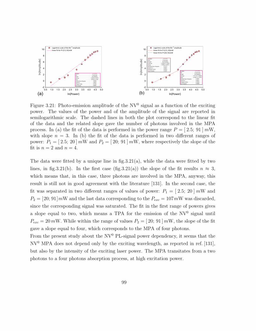
0.5 1.0 1.5 2.0 2.5 3.0 3.5 4.0 4.5 5.0-2
0
2
4
6
8
10 Logaritmic scale of the NV 0 amplitude linear fit for P=[2.5; 91]mW
ln(Amplitu
de)
ln(Power)
Equation y = a + b*xPlot ln (real amp)Weight No WeightingIntercept -7.61116 ± 0.59623Slope 3.81861 ± 0.15155Residual Sum of Squares 0.25851Pearson's r 0.99531R-Square (COD) 0.99064Adj. R-Square 0.98908
Equation y = a + b*x
Plot ln (real amp)
Weight No Weighting
Intercept -4.30479 ± 0.53197
Slope 2.97193 ± 0.1576
Residual Sum of Squares 3.90692
Pearson's r 0.98623
R-Square (COD) 0.97265
Adj. R-Square 0.96991
(a)0.5 1.0 1.5 2.0 2.5 3.0 3.5 4.0 4.5 5.0
-2
0
2
4
6
8
10 Logaritmic scale of the NV 0 amplitude linear fit for P=[2.5; 20]mW linear fit for P=[20; 91]mW
ln(Amplitu
de)
ln(Power)
Equation y = a + b*xPlot ln (real amp)Weight No WeightingIntercept -7.61116 ± 0.59623Slope 3.81861 ± 0.15155Residual Sum of Squares 0.25851Pearson's r 0.99531R-Square (COD) 0.99064Adj. R-Square 0.98908
Equation y = a + b*x
Plot ln (real amp)
Weight No Weighting
Intercept -4.30479 ± 0.53197
Slope 2.97193 ± 0.1576
Residual Sum of Squares 3.90692
Pearson's r 0.98623
R-Square (COD) 0.97265
Adj. R-Square 0.96991
Equation y = a + b*x
Plot ln (real amp)Weight No WeightingIntercept -2.38608 ± 0.43545Slope 1.90062 ± 0.20819Residual Sum of Squares 0.31313Pearson's r 0.98247R-Square (COD) 0.96525Adj. R-Square 0.95367
(b)
Figure 3.21: Photo-emission amplitude of the NV0 signal as a function of the excitingpower. The values of the power and of the amplitude of the signal are reported insemilogarithmic scale. The dashed lines in both the plot correspond to the linear fitof the data and the related slope gave the number of photons involved in the MPAprocess. In (a) the fit of the data is performed in the power range P = [ 2.5; 91 ]mW,with slope n = 3. In (b) the fit of the data is performed in two different ranges ofpower: P1 = [ 2.5; 20 ]mW and P2 = [ 20; 91 ]mW, where respectively the slope of thefit is n = 2 and n = 4.
The data were fitted by a unique line in fig.3.21(a), while the data were fitted by two
lines, in fig.3.21(b). In the first case (fig.3.21(a)) the slope of the fit results n ≈ 3,
which means that, in this case, three photons are involved in the MPA, anyway, this
result is still not in good agreement with the literature [131]. In the second case, the
fit was separated in two different ranges of values of power: P1 = [ 2.5; 20 ] mW and
P2 = [20; 91]mW and the last data corresponding to the Pexc = 107mW was discarded,
since the corresponding signal was saturated. The fit in the first range of powers gives
a slope equal to two, which means a TPA for the emission of the NV0 signal until
Pexc = 20mW. While within the range of values P2 = [ 20; 91 ]mW, the slope of the fit
gave a slope equal to four, which corresponds to the MPA of four photons.
From the present study about the NV0 PL-signal power dependency, it seems that the
NV0 MPA does not depend only by the exciting wavelength, as reported in ref. [131],
but also by the intensity of the exciting laser power. The MPA transitates from a two
photons to a four photons absorption process, at high excitation power.
99
Chapter 4
Structural and optical properties of
ZnO/MgZnO heterostructures
4.1 Introduction
Wide bandgap semiconductors rised in the recent years, increasing the production of
high-power and high-frequency electronic devices (e.g. lasers and diodes).
The successful progress of this class of materials has come to the forefront thanks to the
parallel improvement of the growth techniques, which allow to reach a better control
on the growth parameters and then on the high quality of the grown materials.
One material whose research and study was largely boosted and expanded in the last 20
years is the zinc oxide (ZnO). Indeed, ZnO can now be grown, as bulk crystal, thin film
and also as nanostructure, with a variety of techniques [134]. Among them, the Molec-
ular Beam Epitaxy (MBE) leads to the availibility of large area single bulk crystals and
also high quality of thin films, with reduced concentration of extended defects. The
open issue in the growth of bulk crystals and thin films is the need to employ a material
with a lattice substrate which causes limited number of lattice defects in the grown one,
due to the lattice mismatch related to the two materials, which can be exacerbated by
their competing thermal expansion mismatch. In order to overcome the substrate prob-
lem a possible solution is the use of low scale systems materials, likes nanostructures
100

[134, 135]. The nanoscale systems can be strain free, offering more flexibility in strain
engineering and also present efficient carrier confinement [135], in the case of quan-
tum confined systems. In this chapter the quantum well, grown in a heterostructure
of ZnO/MgZnO materials will be discussed in detail. In general, thanks to their pe-
culiar characteristics (e.g. geometry, electronic distribution and surface/volume ratio),
quantum confined systems are advantageous in order to enhance the opto-electronic
performances of the new devices, as in the case of LEDs, and they can also find good
applications as sensors [136, 137]. The rising importance of this low scale technology
asks to pay particular attention also to the development of techniques able to probe
with high spatial resolution the crystalline structure of these materials and also their
physical properties.
In this chapter the main optical properties of quantum well heterostructures of ZnO/MgZnO,
are linked to the crystalline structure of the analyzed material thanks to the recent
experimental developments on correlative laser-assisted atom probe tomography and
optical spectroscopy “in-situ” [138, 57]. The system, named “µ−PL/La-APT”, has the
advantages to determine the average alloy composition, compositional fluctuations in
three dimensions, with sub-nanometer spatial resolution and the optical signature of
the sample, during the experiment. The nano-specimen has to be a nanoscale volume
of a sharp material tip (as seen in Chapter 1) and the 3D virtual reconstruction of the
sample is performed through the elaboration of the collected data, in order to access
to the constituent chemical species, size and shape of it and to correlate these features
with the optical transitions characteristic of the studied system. The optical transis-
tions of one material is the fingerprint of the distribution of its electronic states which
are influenced by the structure of the material itself. It follows that probing a nanos-
tructure through the µ−PL/La-APT setup the structural and physical properties (e.g.
electronic, optical, mechanical, thermal) of the probed specimen can be outlined in only
one experience.
101
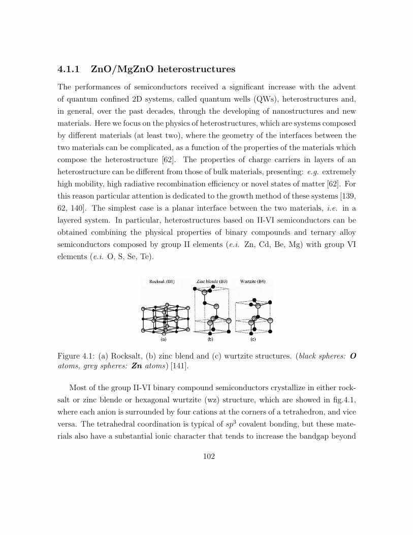
4.1.1 ZnO/MgZnO heterostructures
The performances of semiconductors received a significant increase with the advent
of quantum confined 2D systems, called quantum wells (QWs), heterostructures and,
in general, over the past decades, through the developing of nanostructures and new
materials. Here we focus on the physics of heterostructures, which are systems composed
by different materials (at least two), where the geometry of the interfaces between the
two materials can be complicated, as a function of the properties of the materials which
compose the heterostructure [62]. The properties of charge carriers in layers of an
heterostructure can be different from those of bulk materials, presenting: e.g. extremely
high mobility, high radiative recombination efficiency or novel states of matter [62]. For
this reason particular attention is dedicated to the growth method of these systems [139,
62, 140]. The simplest case is a planar interface between the two materials, i.e. in a
layered system. In particular, heterostructures based on II-VI semiconductors can be
obtained combining the physical properties of binary compounds and ternary alloy
semiconductors composed by group II elements (e.i. Zn, Cd, Be, Mg) with group VI
elements (e.i. O, S, Se, Te).
Figure 4.1: (a) Rocksalt, (b) zinc blend and (c) wurtzite structures. (black spheres: O
atoms, grey spheres: Zn atoms) [141].
Most of the group II-VI binary compound semiconductors crystallize in either rock-
salt or zinc blende or hexagonal wurtzite (wz) structure, which are showed in fig.4.1,
where each anion is surrounded by four cations at the corners of a tetrahedron, and vice
versa. The tetrahedral coordination is typical of sp3 covalent bonding, but these mate-
rials also have a substantial ionic character that tends to increase the bandgap beyond
102

the one expected from the covalent bonding. ZnO is a II-VI compound semiconductor
whose ionicity resides at the borderline between the covalent and ionic semiconductors.
ZnO can assume either the wurtzite structure or the zinc blende or the rocksalt crystal
structure, as a function of the different conditions (T, p) at which it is exposed. Un-
der ambient conditions the thermodinamically stable phase is that of wurtzite. The
zinc blende ZnO structure can be stabilized growing ZnO on cubic substrate, while the
rocksalt phase of ZnO is obtained only at relatively high pressures. Here we report
about the wz ZnO structure which has a hexagonal unit cell, fig.4.2, with two lattice
parameters a and c, in the ratio ca=
√
83= 1.633 (in an ideal wurtzite structure), and
it belongs to the space group C46v in the Schonflies notation. The group C4
6v preserves
the symmetry of the crystal including rotations by: ±60, ±120 and ±180 around
the hexagonal axis. The basal plane lattice parameter (edge length of the basal plane
hexagon) is universally depicted by a; the axial lattice parameter (unit cell height),
perpendicular to the basal plane, is universally denoted as c, as shown in fig.4.2.
Figure 4.2: (a) Unit cell of the wurtzite structure, the two lattice parameters a andc and the u cell-internal parameter are indicated: yellow spheres are referred to Zn
atoms and black spheres to O atoms. (b) Another conventional unit cell representationof the ZnO bulk material including the definition of the most relevant low-index crystal-surface planes. The polar c-plane and the two nonpolar m− and a-planes are shown inblue, red, and green, respectively.
103

The structure is obtained interpenetrating two hexagonal close-packed (hcp) sublat-
tices (fig.4.2), each of which consists of one type of atom displaced with respect to each
other along the threefold c-axis by the amount of a quantity labeled as u = 38= 0.375
and called cell-internal parameter [141]. Each sublattice includes four ions per unit
cell, every ion of one kind (group II, e.i. Zn) is surrounded by four ions of other kind
(group VI, e.i. O) or vice versa, the ions are coordinated at the edges of a tetrahedron.
In real ZnO crystal, the wurtzite structure deviates from the ideal arrangement, by
changing the caratio and so the value of the lattice parameters a and c. These param-
eters don’t deviate drastically from the theoretical value, but their ratio, ca, is included
within the range [1.593; 1.6035] [141] and the deviation from that of the ideal wurtzite
crystal is probably related to lattice stability and ionicity [141]. Between the caratio
and the u parameter a strong correlation exists, indeed when the caratio decrease, the
u parameter increases in order to let four tetrahedral distances remain nearly constant
through a distortion of tetrahedral angles. The difference between the the real value of
u = [0.383; 0.3856] [141] and the ideal value uideal = 0.375 is defined as ǫ1 = u− uideal.
The ǫ1 quantity was found to significantly affect the spontaneous polarization, Pspont,
along the c-axis, in the wurtzite structure [62]. The origin of this kind of polarization
in the wurtzite crystal structure is the intrinsic asymmetry in the relative arrangement
of the Zn and O ions along the c-axis, [0001] direction. For that reason, the c-axis is
called “polar direction”, while the a-axis, [1120] direction, and m-axis, [1100] direction,
are non-polar axes [134], fig. 4.2.
The spontaneous polarization of ZnO cannot be directly measured [142], however when
mechanical stress is applied on the surface of the wurtzite structure, the piezoelectric
reponse of the material gives rise to the piezoelectric polarization reponse, Ppiezo. The
total effect of the contribution of the induced and the spontaneous piezoelectric po-
larization can then be measured and the total polarization Ptot is defined in equation
(4.1):
Ptot = Pspont + Ppiezo (4.1)
The properties of band structure are determined by the symmetric properties of the
semiconductor crystal and chemical binding of constituting elements. Based on the
104

atomic orbitals, the conduction band EC is mainly constituted by first unoccupied s-
levels or antibinding states, which derives usually from the cations, such as the 4s
levels of Zn in ZnO. The corresponding valence bands EV are formed by the highest
unoccupied levels, which are p-levels or binding states, such as 2p-levels for the O in
ZnO. The band structure of ZnO near the Γ of the Brillouin zone is depicted in fig.4.3,
where the band structure E(k) is expressed as a function of the k quasi-momentum.
As shown in figure 4.3 (b), at Γ, three degenerate valence bands, EV , coesist and
by uniaxial crystal field of hexagonal wz crystal structure and by spin-orbit coupling,
they are splitted in: heavy holes (hh), light hole (lh) and split-off holes (s-o) states.
These electronic states are also labeled, in literature [62]:“ A-band”,“ B-band” and “
C-band”, as in fig.4.3(b), from higher to lower energies. Since ZnO is a direct bandgap
semiconductor, the energy difference between the bottom of the conduction band, EC ,
and the top of the heavy hole state at the Γ point is the material bandgap.
Figure 4.3: (a) Band structure of ZnO in wurtzite structure, calculated using the HSEhybrid functional [134]. The energy of the valence-band maximum (VBM) was set tozero. As a direct bandgap material, the bandagap of ZnO is calculated along the Γdirection of the Brillouin zone. (b) Simplified band structure with conduction band andthree valence bands of ZnO. Zoom in a surrounding of the Γ point in the Brillouinzone depicted on the left (a).
105

As said above, the electronic band structure of a semiconductor depends on its
chemical composition and on its crystalline structure. This means that, for example,
polytypes with identical composition, but different crystal structure, have different en-
ergy gap. It also means that the bandgap can be continuously tuned by controlling the
chemical composition of binary, ternary or quaternary alloys during the synthesis of the
material. Modern heterostructures are often systems based on the alternated growth of
binary compounds and ternary alloys. In order to avoid to grow heterostructures with
extended defects, the lattice mismatch and the crystal quality of the single components
has to be taken into account.
Comparing the size of the bandgap between II-VI semiconductors, as reported in fig.4.4,
at ambient conditions, in wz crystal structure, ZnO presents wide direct bandgap energy
Egap = 3.4 eV and large exciton binding energy Eexc = 60 meV; these characteristics
allow to use this semiconductor as an active (emitting) element in optoelectronic, which
provides ultraviolet (390nm) excitonic laser action upon optical pumping at room tem-
perature. As reported in ref. [134], over the past decades, a significant improvement in
the quality of ZnO single-crystal substrates and epitaxial films was achieved and the
epitaxy of ZnO films on native substrates can result in ZnO layers with reduced con-
centration of extended defects and, so, better performance in electronic and photonic
devices [143]. Thanks to the improvements achieved in the epitaxial growth techniques,
heterostructures containing ZnO alternated to a different material can be grown. The
most important parameters to be checked for a heterostructure are:
• the lattice mismatch between the two grown materials;
• the bandgap of each layer and the valence and conduction bands band offset
between individual layers.
Bandgap engineering in ZnO can be achieved by alloying with MgO and/or CdO. By the
way the MgO and CdO assume the rock-salt structure, not the same crystal structure
of ZnO (wz) and this can generate a big issue for ZnO-based alloys with high content of
MgO and CdO. With a moderate content of MgO and/or CdO in the ZnO wz structure,
the MgZnO and CdZnO alloys assume the wz crystal structure of the parent compound,
still providing a wide range of bandgaps : [3.2; 4.1] eV [134]. The ternary alloy can be
106
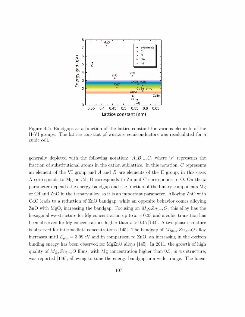
Figure 4.4: Bandgaps as a function of the lattice constant for various elements of theII-VI groups. The lattice constant of wurtzite semiconductors was recalculated for acubic cell.
generally depicted with the following notation: AxB1−xC, where ‘x’ represents the
fraction of substitutional atoms in the cation sublattice. In this notation, C represents
an element of the VI group and A and B are elements of the II group, in this case:
A corresponds to Mg or Cd, B corresponds to Zn and C corresponds to O. On the x
parameter depends the energy bandgap and the fraction of the binary components Mg
or Cd and ZnO in the ternary alloy, so it is an important parameter. Alloying ZnO with
CdO leads to a reduction of ZnO bandgap, while an opposite behavior comes alloying
ZnO with MgO, increasing the bandgap. Focusing on MgxZn1−xO, this alloy has the
hexagonal wz-structure for Mg concentration up to x = 0.33 and a cubic transition has
been observed for Mg concentrations higher than x > 0.45 [144]. A two phase structure
is observed for intermediate concentrations [145]. The bandgap of Mg0.33Zn0.67O alloy
increases until Egap = 3.99 eV and in comparison to ZnO, an increasing in the exciton
binding energy has been observed for MgZnO alloys [145]. In 2011, the growth of high
quality of MgxZn1−xO films, with Mg concentration higher than 0.5, in wz structure,
was reported [146], allowing to tune the energy bandgap in a wider range. The linear
107

relationship between bandgap and Mg-II site fraction was established, for the hexagonal
phase [147], to be (eq.4.2):
Egap(MgxZn1−xO) = Egap(ZnO) + b · x (4.2)
where b = 2 eV. The Mg-II site fraction also changes the wz-lattice constants, indeed
as the Mg concentration increases as the lattice parameter a increases and c decreases
[148]. In figure 4.5(a) is plotted the relationship between the values of the a and c
lattice parameters and the Mg concentration in MgxZn1−xO, while in figure 4.5(b) is
plotted the dependence of the energy bandgap of theMgxZn1−xO alloy on the Mg con-
centration, in the case of wz crystal structure and also for the rocksalt crystal structure.
In table 4.1, the main structural and optical properties of the ZnO, MgO and
Figure 4.5: (a) Dependence of the a-lattice and c-lattice parameters and of (b) thebandgap on the Mg II-site fraction y (images readapted from ref. [145])
MgxZn1−xO are summarized and can be compared.
4.1.1.1 Band alignement in ZnO/MgZnO heterostructures
Heterostructures based on ZnO/MgxZn1−xO are currently employed in the developing
of systems and devices based on quantum confined effects and on interband or intersub-
band transitions, as it will be explain in the section 4.1.2. Before to treat the optical
108

ZnO MgO MgxZn1−xO
Egap(eV) 3.4 7.8 3.37+2·x [149]
a (nm) 3.2 4.2 3.25+0.036·x [149]
c (nm) 5.2 . . . 3.34-0.063·x [148]
stable crystal wurtzite rocksalt x ≤ 0.33 or x < 0.5 wurtzite [147]structure 0.33 < x < 0.45 rocksalt [147]
Table 4.1: Main structural and optical characteristics of ZnO, MgO and MgxZn1−xOat T = 300K
properties of inside the quantum well (QW) or multi quantum well (MQW) system, it
is important to visualize how the bandgaps of the ZnO and MgZnO are aligned at the
heterojunctions between the two materials or properly inside the heterostructure.
As known, ZnO and MgxZn1−xO are semiconductors with different bandgaps, which
are grown in an ordered hierarchical way, alternating layers of one material with the
second one. The two materials might have not only different bandgaps, but also differ-
ent thickness: the thinner semiconductor, if it has thickness below the value of the “de
Broglie wavelength”’ (λde B ≈ 10nm) and it has the lower bandgap value, constitutes the
QW, while the thicker semiconductor, if it has thickness above 10nm and the bandgap
has the wider value, is called barrier of the QW. The relative position of the conduction
and valence band, between the two semiconductors, (band alignment) is determined
through the electron affinities χ, as depicted in fig.4.6.
The semiconductor electron affinity is the (positive) energy difference between the
vacuum level and the conduction band edge. as a function of the different type of
bands alignment, two kind of heterostructures are distinguished: type-I and type-II
heterostructures. In the type-I structure, the lower conduction-band edge and the
higher valence-band edge are both in the material with smaller band gap. In this way,
electrons and holes localize there. In type II structure, a staggered lineup is present
and electrons and holes localize respectively in the different materials. In the case of
MQWs systems of ZnO/MgxZn1−xO, we are considering a heterostructure of type I. At
ambient conditions (p, T ) and as wurtzite crystal structure, ZnO has a bandgap equal
109

Figure 4.6: Position of band edges (band alignment) in (a) type-I and (b) type-IIheterostructure.
to 3.37eV, while theMgxZn1−xO bandgap varies as a function of the x concentration of
Mg, as reported in the plot in fig.4.5(b). The bandgap of MgxZn1−xO as a function of
x was observed to vary within the range: [3.37; 3.99] eV, where the bandgap increasing
up to 3.99 eV is observed for MgxZn1−xO wurtzitic structure for Mg concentration x =
0.33 [134]. The ZnO layers act as QWs and the layers ofMgxZn1−xO as barriers of the
QWs, appropriately tuning the growth conditions of the heterostructure. Unfortunately,
as wurtzite layers, ZnO/MgxZn1−xO heterostructures exhibit built-in electric fields
along the c-axis [0001] and this characteristic inevitably affects the electronic properties.
So, in order to avoid this kind of limitation one strategy could be to grow the wurtzitic
ZnO/MgxZn1−xO heterostructure using the non-polar a-axis or m-axis direction of
growth. One important condition to tune in order to take advantage on the choice of the
non-polar direction of growth is to precisely control the strain state of the MgxZn1−xO
barrier, as a function of its layer thickness and x Mg concentration [150, 151], because
the effect of the residual strain in non-polar layers of ZnO QWs is reflected on the QWs
band structure, as explained by Chauveau et al. [150]. In particular, the (Mg,Zn)O
samples investigated by Chauveau et al. [150], grown along nonpolar a-(1120) or m-
(1100) directions by metal organic chemical vapor deposition (MOCVD), showed an
evolution of the in-plane lattice parameter along the c- and m-directions until Mg
concentration xMg ≈ 25 % and then the in-plane c-lattice parameter stabilizes. The
110

evolution of the c- and m- lattice parameters, for increasing xMg concentrations (0 <
xMg < 0.25), has an anysotropic trend. Such anisotropy of lattice parameters generates:
• tensile strain, along the m-axis [1100];
• compressive strain, along the c-axis [0001].
This strain has an effect on the QWs that corresponds to a strong blueshift of the exci-
tonic levels, which gives rise to a blue-shift effect in the QW-PLE signal, in agreement
with the theory of the quantum well confinement and localization effects.
4.1.2 Carriers distribution inside the ZnO quantum wells
A QW is a thin flat layer of a semiconductor (typically below the size of the “de Broglie
wavelength”) , that is grown between two thicker layers of different semiconductors,
which constitute the barriers of the QW. In figure 4.7 is represented the electronic
distribution in the conduction and valence bands at the heterojunction between a QW
and the barriers related to a heterostructure of type I, like ZnO/MgxZn1−xO, where
Egap,barr > Egap,QW .
As we can observe in fig.4.7, carriers in a quantum well are confined only on the
growth direction, z-axis, but they can freely move along the quantum well plane (x, y).
The carriers thus possess in-plane energy levels which depend on their in-plane wave
vector k and they are distributed in 2D bands. Neglecting the lattice periodic wave
function, the total carrier envelope function is the product between the confined wave
function ψn(e,h)(z) and a plane wave exp(ik·r), with r=(x,y). The Schrodinger equation
of the system (eq.4.3), where r = (x, y, z), can be splitted and solved separately for the
in-plane and the on-axis components.
h2
2m· d
2ψ(r)
dr2+ (E + V (r)) · ψ(r) = 0 (4.3)
The on-axis (z) solution yields a set of discrete levels, called subbands. The subband
energy can first be estimated by approximating the barriers as infinitely high. In this
ideal case, the energy En(e,h) of the electron/hole subbands can be indexed as follows
111

Figure 4.7: (a) Confined electron and hole energies and wave functions (sub-bands)within a rectangular quantum well of a given composition and thickness. Parts (b) and(c) show how the energy of the states and of the main radiative recombination evolveswith quantum well composition and thickness, respectively.
(eq.4.4):
En(e,h) =h2π2n2
m∗e,ht
2QW
n = 1, 2, 3... (4.4)
while the wave functions ψn(e,h)(z) are completely confined within the quantum well
and are given by the relation (4.5):
ψn(e,h)(z) = Azsin
(
πnz
tQW
)
(4.5)
where An is the normalization constant satisfying the condition that integral of the
squared wave function over z is equal to unity. In the (eq.4.4), m∗e,h is the electron
(hole) effective mass, which represents the electron mass of an electron inside of a
crystal, where the electron interacts with the crystal fields. The electron (hole) effective
mass differs from the mass of a free electron, of the classical equation: E = p2
2m, but
it allows to treat the electrons (holes) inside of a crystal as if they are free, for some k
112

values. The m∗e,h electron (hole) effective mass is defined in the equation (4.6).
m∗e,h =
(
1
h2∂2E
∂k2
)−1
(4.6)
As we can read in the equation (4.6), the m∗e,h electron (hole) effective mass results pro-
portional to the slope of the energy band where the electron can move, so it depends
on the QW composition.
One of the main effects of the quantum confinement is that the electron and hole ground
states do not lie at the bottom of the conduction or valence bands characteristic of the
QW phase, but are lifted of a certain amount, fig.4.7, which is called the confinement en-
ergy E1(e, h). As illustrated in fig.4.7(b) and (c), the electronic wave function becomes
progressively less confined with decrease of barrier gap. Furthermore, a finite number
of subbands can be accomodated in a QW with finite barrier height. The main optical
emission taking place within a quantum well involves the electron and hole “ground
states” (n = 1). The emission energy is given from (4.7):
Ee,h = E1e + E1h + Eg, QW (4.7)
The terms which appear in the equation (4.7) all depend on the barrier composition
and on the quantum well thickness tQW . In the equation 4.7, the E1ex term is omitted
and this term, which labels the exciton binding energy, will be discussed in the next
section more in detail. Looking at the pictures 4.7(b) and (c) and the equation (4.7) is
clear that the QW confinement energy spacing becomes large for narrow wells (small
tW ) and small effective mass m∗e,h, while it reduces incresing the well thickness and
effective mass. Real quantum wells are more complex than the basic description and
representation given here. For instance, in real QWs, the finitness of the barrier energy
gaps yields an evanescent but non-zero wave function within the barriers and a decrease
of the subband energy En. Alloy clustering within the quantum wells may occur and
defects can be present as well. But, since the QWs size is usually less than 10 nm,
the critical thickness to form dislocations in non-lattice matched epitaxial layers is
never reached. This allows the growth of high quality non lattice-matched materials.
113

Alternating QWs with barriers leads to the formation of MQWs. The physics of MQWs
is essentially the same as a set of single QWs. However, if the barriers are too thin,
the wavefunctions associated to the confined states penetrates in adjacent QWs which
form a periodic system called superlattice.
Another interesting consideration to do is about the effect of external or internal fields
acting on the electronic states within a QW. For instance, QWs grown along a crystal
direction with no inversion symmetry, as the in the case of wz crystal, exhibit polar
properties leading to the Quantum Confined Stark Effect (QCSE). In that case, a
spontaneous polarization develops and such polarization has opposite direction for the
different heterostructure phases, a static sheet charge builds up at heterointerfaces. This
spontaneous polarization is known also as pyroelectric effect and the sign of the charge
depends on: the polarization values of the ZnO and MgxZn1−xO, which compose the
interface, and whether the ZnO is before or after the MgxZn1−xO along the polar
direction.
Figure 4.8: (a) Confined electron and hole energies and wave functions (sub-bands)within a rectangular quantum well exhibiting the buidup of an internal field (the termEe,h refers to a zero-field system. (b) Confined electron and hole energies and wavefunctions (sub-bands) within a rectangular quantum well across which an external fieldis applied.
Furthermore, along the growth direction each heterostructure phase is coherently
strained on another and such strain may set up a further polarization, which increases
114

the concentration of carriers at the interfaces, as consequence of the piezoelectric effect.
These carriers confinement translates into the presence of an electric field within the
QW structure or, better, as an electric field discontinuity across the heterointerface, as
shown in figure 4.8(a).
The effect of this internal electric field, shown in fig.4.8(a), which acts on the electronic
states of the QW translates in shifts of the radiative recombination energy and intensity.
The modification to the energy levels also depends on the thickness of the quantum well
structure. If we consider the non-polar directions, which are the a-axis and m-axis in
the wurtzite crystal, the QCSE is present only if an external electric field is acting
on the quantum confined system. The potential profile at the heterointerface and the
confined electron and hole wavefunctions are modified as effect of the electric field acting
on them. Indeed, the electric field reduces the electron and hole energies with respect
to the flat-band case and it spatially separates the wave functions of electron and hole.
Differently from the effect of an internal electric field, comparing figures 4.8(a) and
(b), it is clear that an external electric field tilts the valence and conduction bands of
the barriers and QWs along the same direction, fig.4.8(b), reducing the electron-hole
wavefunctions overlap, affecting also the optical properties of the system. Wurtzitic
heterostructures of ZnO/MgxZn1−xO, grown along the c-axis, due to the polarization
presents along this crystallographic orientation, they have a built-in electric field that
affects inevitably the optical/electronic properties of the system. Using the non-polar
a − [1120] or m − [1100] surfaces of growth can avoid this limitation. In such case,
in order to take advantage of non-polar heterostructures, it is a prerequisite to control
precisely the strain state of the MgxZn1−xO barrier and the residual strain acting on
non-polar ZnO QWs, as explained in the article [150].
4.1.2.1 Excitons
In the ideal case, at T = 0 K, the ground state of a semiconductor is depicted by
the filled valence band EV and the empty conduction band EC . The absorption of a
photon causes the transition of an electron in the conduction band and leaves a hole in
the valence band.
115

If the characteristic thermal energy (kBT ) is sufficiently low, taking in account the
effective mass m∗e,h model, the pair of excited electron and hole interacts each other
through Coulomb field and form an hydrogen-like state called exciton. This bound
state, exciton, induced by the attractive potential is characterized by an energy (4.8):
Enex = −
R∗y
n2+h2k2
2Mwith : M = me +mh (4.8)
R∗y is called Rydberg energy and it is defined as: R∗
y = 13.6 µmo·ǫ2
(eV) and µ = me·mh
me+mh
.
The radius of the exciton is given by the equation (4.9):
rnex = n2m∗e
µǫraB (4.9)
where aB = 0.53 nm denotes the hydrogen Bohr radius and for the exciton the parallel
one is r1ex.
Two main catergories of excitons can be distinguished:
• free excitons : if the excitons can move freely inside the semiconductor;
• bound excitons : if the excitons are associated with point defects of the semicon-
ductor.
Figure 4.9: Temperature-dependent luminescence spectra of ZnO thin film. At lowtemperatures, the PL signal is dominated by donor-bound exciton transitions. Thecurved dashed line visualizes the energy position of the free-exciton transition (XA),that becomes dominant at room temperature.
116
Excitons play an important role in optical properties of semiconductors, especially at
low temperature, where the exciton recombination is the main mechanism for the light
emission. Particular is the case of ZnO, where the recombination from free-excitons is
observed even at room temperature, as shown in figure 4.9. This phenomenon will be
explained better in the next section 4.1.3.
When the characteristic thermal energy (kBT ) of a semiconductor increases, the exciton
interaction is replaced by the electron-hole recombination.
In QWs, the exciton radius eq.(4.9) is lower than in bulk materials, at least in the
direction perpendicular to the QW, so the exciton binding energy may increase up to
4 times as large as the bulk value. Furthermore, the ZnO excitonic binding energy
(60meV) can be increased up to 120meV in the ZnO/MgZnO MQs, due to quantum
confinement effects [140].
4.1.3 Carrier localization and radiative recombination in ZnO/MgZnO
heterstructures
As previously seen, the energy bands of a semiconductur system (e.g. binary compound,
alloy, heterostructure..) are determined by its crystal structure and chemical binding
of the constituting elements. Some structural features (e.g. alloy disorder, defects, dis-
locations...) and compositional fluctuations at the layer interface, in a heterostructure,
may lead to formation of local minima in the material band structure, where carriers can
localize and radiatively recombine. As demonstrated in the case of the MgZnO alloy,
by Y. Hu et al. [152], alloying of the ZnO wurtzitic crystal with different concentration
‘x’ of Mg can be done in two possible ways: the Mg atoms can substitute the Zn ions in
the ZnO crystal lattice or they can be partially incorporated in interstitial positions. In
both cases, the concentration ‘x’ of Mg, in theMgxZn1−xO alloy, affects the structural,
electronic and optical properties of the ternary alloy. In the case of interstitial Mg-
doping it has been proved that MgxZn1−xO conductivity increases until x < 15.89 %,
while it abruptly decreases for x above that value. This phenomenon, which inevitably
affects the electronic and optical performance of the system, provocates local minima
or deformation of the energy band as a function of the local Mg-doping in the ZnO
117

structure. One way to observe and measure the localization energy, in an alloy or at
the heterointerfaces of a heterostructure, consists in varying the temperature in a cer-
tain range of values, for example as reported in the articles [153, 154, 139], from few
Kelvin until room temperature. Indeed, at very low temperature carriers are trapped
in local minima of the band structure and their thermal energy is not enough to move
from one minimum to a deeper one. Such situation is called“freeze up” regime, depicted
in figure 4.10(I). If we study the photoluminescence signal of the electron hole recom-
bination, it corresponds to the average of the localized energy states. Increasing the
Figure 4.10: Scheme of interband transitions at different temperatures, in presence ofalloy compositional fluctuations.
temperature, the bandgap is reduced following the Varshni’s empirical law [62], and we
enter into the “thermalization” regime, fig. 4.10(II). In this regime the carriers trapped
in local minima have enough energy to thermalize (jump) to the lowest minimum in
their neighbors and, as consequence, the recombination energy is decreased with re-
spect to the Varshni’s empirical law of a quantity which corresponds to the localization
energy Eloc, as represented in fig. 4.10(II). Then increasing more the temperature free
carriers can recombine and the electron hole recombination is in agreement with the
estimated value through the Varshni’s law, this situation corresponds to the “delocal-
ization” regime, fig. 4.10(III). The transitions between different recombination regimes
produces the characteristic “S-shape” in the photoemission signal.
In figure 4.11 are reported the PL spectra related to evolution of the Zn0.85Mg0.15O −ZnO−Zn0.85Mg0.15O signal at different thermal ranges: TI=[10; 50] K, TII=[70; 150] K
and TIII >150 K. Looking at the peak related to the ZnO-single quantum well (SQW),
fig. 4.11, its energy first (TI range) shows a redshift and then a blue shift (TII range)
followed by an another redshift, at T>150 K, exhibiting the so-called “S-shape” [154].
118

In the article [154], the ‘S-shape’ behavior is explained within the model of localized
Figure 4.11: PL spectra of a Zn0.85Mg0.15O − ZnO − Zn0.85Mg0.15O sample from thearticle [154]. The S-shape shift with increasing temperature is indicated by the orangearrow.
excitons, in agreement to what reported above and depicted in figure 4.10. In the Zn-
MgO/ZnO/ZnMgO heterostructure, at the lowest temperatures, excitons are localized
even in shallow lateral potential fluctuations due to the roughness of the ZnMgO-ZnO
interfaces. When the temperature increased, excitons from shallow lateral potential
fluctuations are delocalized and they can diffuse to regions with larger well widths and
hence lower transition energies (redshift) with respect to the bandgap evaluated by
the Varshni’s law [62]. The excitonic transitions in correspondence of regions of local
minima of the bandgap is dominant at intermediate temperatures and the overlapping
of this region, which corresponds to the blueshift photoemission, gives a PL emission
in agreement with the bandgap energy, according to the Varshni equation [62]. The
‘S-shape’ behavior in the ZnO/MgZnO heterostructure was investigated along both the
c- and m-axis directions [155]. In a quantum confined system, such as a QW, the carrier
localization phenomenon asks to take into account more conditions. First we have to
take into account that the emission energy is shifted towards higher energy, eq. (4.10),
compared to the energy bandgap of the semiconductor constituting the well.
EPL,QW = Egap + E1hh + E1
e − E1ex (4.10)
119

E1hh is the energy related to the first excited state in the valence band, for heavy holes,
and E1e is the energy of the first excited state in the conduction band, while E1
ex is the
exciton binding energy. In agreement with the equations (4.4) and (4.10), the energy
bandgap of the QW can be tuned choosing its well thickness ‘tQW ’. Furthermore it
has to be considered in case of polar QW heterostructures, e.g. ZnO/MgZnO, if the
QW-growth direction is along a polar plane or not. If the structure is grown along
a polar direction, then the QW results affected by QCSE which reduces the electron-
hole wavefunction overlaps and decreases the intensity of the PL emitted signal or the
probability of the electron-hole recombination, as reported in the article [156]. In order
to avoid the QCSE, heterostructures should be grown on non-polar planes. It’s clear
that carrier localization phenomena inside QWs can lead to significant variations of the
emission energy. In the MgxZn1−xO alloy, localization phenomena can be related to
local variations of theMg concentration ‘x’. Indeed usually, the concentration in alloys
is not perfectly uniform and the PL emission signal usually comes from regions of the
alloy, where the Mg concentration is lower and the MgZnO energy gap decreases its
value.
4.1.4 Stress and Strain tensors of hexagonal systems
The deformation of a crystal lattice under the effect of an applied mechanical force can
be described in terms of the relative displacements of the atoms of the lattice. This
displacement of the ions that compose the crystal is accompanied by a new disposition of
the electrons. In agreement with the classical theory of the elasticity, we can ignore the
microscopic atomic structure of a crystal and consider it as a continuous medium [62].
Therefore a general deformation of the solid can be described in terms of a continuous
displacement field ~u(~r), specifying the vector displacement of the part of the solid that
has the ~r vector as equilibrium position. In particular, for a single atom placed at ~r, in
an arbitrary Cartesian system, the new position ~r′ is defined as (4.11):
~r′ = ~r + ~u(~r) (4.11)
120

When the spatial variation ~∇ · ~u(~r) of the vector ~u is small, the elastic energy can be
written as (4.12):
U =1
2·∫
(∂uj∂xi
· Cklmn ·∂un∂xm
) · d3~r (4.12)
The Cklmn is the tensor of the elastic coefficients. The strain ǫij, defined as (4.13), is
a second rank tensor that gives the displacements relative to all atoms in the crystal
lattice:
ǫij =1
2· (∂ui∂xj
+∂uj∂xi
) with i, j =1, 2, 3 (4.13)
In the equation ui are the displacement vectors along the three axes of the Cartesian
coordinate system. This tensor is referred to as strain tensor and is usually reported in
its matrix form:
ǫ =
ǫ11 ǫ12 ǫ13
ǫ21 ǫ22 ǫ23
ǫ31 ǫ32 ǫ33
(4.14)
By definition (4.13) the strain tensor is symmetric ǫij=ǫji. The diagonal terms
(normal strain components) represent extension along the axis x1, x2, x3, while the off
diagonal terms (shear or strain components) are related to rotations. The stress tensor
represents the force applied per unit area of the crystal. This force, that can be due
to an external perturbation or can be originated from the interaction of several regions
into the crystal, can be represented as a second-rank tensor, equation (4.16), which is
referred as the stress tensor (4.15):
σ =
σ11 σ12 σ13
σ21 σ22 σ23
σ31 σ32 σ33
(4.15)
Strain and stress tensors are related within the limits of linear elastic theory by the
Hooke’s law:
σij =3
∑
k=1
3∑
l=1
Cijkl · ǫkl (4.16)
121

where the elements of the Cijkl tensor are the elastic coefficients for the linear stress-
strain relationship.
The inverse relation is mediated by the stiffness tensor Sijkl (4.17):
ǫkl =3
∑
k=1
3∑
l=1
Sklmn · σmn (4.17)
The stress and strain tensor has 3×3=9 components each and therefore the elastic
and stiffness matrix has 34= 81 independent elements each.
From the theory of elasticity, the σij components are symmetric under this condition:
σij=σji. Thus the equation (4.16) can be written as follows (4.18):
σji =3
∑
k=1
3∑
l=1
Cjikl · ǫkl (4.18)
Subtracting the (4.16) from the (4.18) leads to the following result: Cijkl=Cjikl. Com-
bining the equation (4.16) with the symmetry property of the strain tensor ǫkl = ǫlk
(4.13), we obtain the new expression (4.19):
σij =3
∑
l=1
3∑
k=1
Cijlk · ǫlk (4.19)
Then comparing the equation (4.19) with the (4.16) we deduce that: Cijkl=Cijlk.
These symmetric properties allow to express the stress and strain relationship as follows
(4.20):
σi =3
∑
k=1
Cik · ǫk (4.20)
122

where[62]:
σ11 = σ1 ǫ11 = ǫ1
σ22 = σ2 ǫ22 = ǫ2
σ33 = σ3 ǫ33 = ǫ3
σ23 = σ4 ǫ23 = ǫ4
σ13 = σ5 ǫ13 = ǫ5
σ12 = σ6 ǫ12 = ǫ6
(4.21)
In this reduced form the Cik matrix consists of 36 independent constants whose
knowledge is important to describe the elastic properties of the considered system.
When the considered system is a crystal, due to the symmetries which characterize the
lattice, the number of independent constants is reduced to 5 for hexagonal systems, as
the wurtzite structure of ZnO. The Hooke’s law then can be respectively expressed as
follows:
σ1
σ2
σ3
σ4
σ5
σ6
=
C11 C12 C13 0 0 0
C12 C11 C13 0 0 0
C13 C13 C33 0 0 0
0 0 0 C44 0 0
0 0 0 0 C44 0
0 0 0 0 0 (C11−C22)2
·
ǫ1
ǫ2
ǫ3
ǫ4
ǫ5
ǫ6
(4.22)
In the case of ZnO wurtzite structure the value of the five independent elastic
constants (C11, C12, C13, C33, C44) that appear into the matrix (4.22) has been largely
investigated in literature [157, 158]. The table 4.2 shows a comparison between the
values of the second order elastic coefficients (SOECs) of ZnO that, as reported in [159],
were obtained through different theoretical models.
4.1.5 Strain effect on band structure of ZnO
The relative displacement of atoms within a crystal lattice affects the electron and hole
states energies and probability distributions in two dfferent ways: by directly modifying
123

SOECs C11(GPa) C12(GPa) C13(GPa) C33(GPa) C44(GPa)
PAW PBE [159] 197.5 112.2 97.9 204.3 34.24
Exp [157] 209.7 121.1 105.1 210.9 42.5
LDA [158] 209 85 95 270 46
Table 4.2: Second-order elastic coefficients of bulk ZnO.
the band structure of the system as the distance between atoms changes and by changing
the polarization properties of the system, so that a non-uniform distribution of charges
is obtained within specific crystal types and along specific directions. Here we focus
on the first case, where the effects of strain are described within the framework of
deformation potential theory, by additional terms in the effective Hamiltonian which
are referred to as deformation potentials.
Deformation potentials:
The Hamiltonian of the strained system can be written as the sum of the unperturbed
Hamiltonian and a contribution induced by strain:
H = H0 +Hǫ (4.23)
where the strain related term can be expressed in terms of the unperturbed crystal
potential V and strain tensor components ǫi,j as:
Hǫ =∑
i,j
∂V
∂ǫi,jǫi,j (4.24)
For (4.24) to hold, the strain and the consequent variations from the unperturbed Hamil-
tonian have to be small. In this case, first-order perturbation theory allows expressing
the relative band shifts (energy shift considered for the valence band) due to strain as a
function of the deformation potential components, as reported in ref. [160, 149]. Both
the conduction and valence band edges are affected by the strain-induced energy shift
and deformation potentials can be defined for the two cases. More details on the way
in which these terms can be generated can be found in literature [161, 162]. It is worth
124

noting that it is not usually easy to have access to the deformation potentials for the
conduction and valence bands, separately. Deformation potentials for the band gap
can thus be defined and the relative contribution from the shifts of the two band can
be issued by first principle calculations [163]. The deformation potentials of the ZnO
valence band (D1, D2, D3 and D4) were derived by Rowe et al. [160] and their values,
are reported in table 4.3.
D1 D2 D3 D4
eV eV eV eV
ZnO −2.66± 0.30 2.82± 0.30 −1.34± 0.30 1.00± 0.30
Table 4.3: Valence band deformation potentials (in eV) of ZnO [160], at T=77 K.
125

Chapter 5
Coupled “in-situ” µPL/La-APT
measurements of the ZnO/MgZnO
MQWs system
5.1 The ZnO/MgZnO sample
The ZnO/MgZnO heterostructure analyzed is a MQW system and, by convention,
ZnO indicates the material which composes the QWs, while MgZnO indicates the
material which forms the barriers. The samples were grown on 10 × 10 mm2 ZnO
substrates, oriented along the non-polar m-plane by plasma assisted molecular beam
epitaxy (MBE), more details about the technique of growth can be found in the ref-
erences [151, 164, 165]. The substrates were annealed at 1065C under an oxygen (O)
atmosphere to reveal the atomic steps. The atomic O was provided by a plasma cell at
420W and its flow was set to 5mm3/s. The substrate temperature was set to 420C.
The Zn and O fluxes were adonlyed with a growth rate of 170nm/h, in order to be close
to the stoichiometry and to limit the defect concentrations. The structures consisted
of a 150 nm ZnO buffer layer followed by 10 periods of ZnO-QW/MgZnO-barrier, as
outlined in fig. 5.1.
The ZnO/MgZnO heterostructure has a wurtzitic crystal structure, the nominal Mg
126

Figure 5.1: Schematic of the hierarchic structure of the ZnO/MgZnOMQW heterostruc-ture.
concentration is 10% and the thickness of the barriers is ≈ 45 nm , while the thickness
of the wells increases if we move from the base of the sample, the position closer to
the substrate, towards the top of the heterostructure. The ZnO layer thickness range
typically from 1.5 to 4 nm and the total length of the MQW heterostructure was kept
below 150 nm in order to avoid plastic relaxation effects. As explained in the previous
section 4.1.1 and in the articles [150, 151], the tuning of the Mg concentration in the
MgZnO barrier plays an important role on the wz-lattice parameters that can give a
residual strain along the c-plane direction and such strain can propagate within the
ZnO QW. When the ZnO/MgZnO MQWs system is grown along the m-nonpolar
direction, the situation is different. Indeed, as H.Matsui et al. [151] have demonstrated,
theMgZnO layers repeat the surface structure of the underlying ZnO layers. Thus the
MgZnO/ZnO interfaces in MQWs are periodically modulated by the substrate array.
Furthermore, as known, as the Mg concentration ‘x’ as the thickness of the QWs can
be choosen respectively to tune the MgZnO and ZnO bandgaps. In the present case,
ranging the thickness of the QWs between 1.5 and 4nm we expect the effective bandgap
between ≈3.9 and ≈ 3.4 eV, while for the MgxZn1−xO barriers,the nominal thickness
is ≈ 45 nm, while the nominal Mg concentration xMg is to evaluate by the PL-spectra,
127

using the equation (4.2), and it can be compared with the value obtained by the APT
reconstruction.
5.1.1 Morphological and structural characteristics of the APT
specimens
In order to investigate the structural, compositional and optical properties of the
ZnO/MgxZn1−xO MQWs system, through the coupled APT-µPL setup, the speci-
mens were prepared following the standard lift-out procedure. The preparation of the
specimen by SEM-FIB was introduced in the section 1.4, Chapter 1. The most im-
portant aspect during the preparation of specimens by focused ion beam (FIB) is to
preserve their structure. Indeed ion implantation can take place, causing amorphiza-
tion/damaging, particularly of the topmost 3-4 periods of the MQW system. In the
worst case, the presence of damaged regions extending the whole surface can lead to
a non radiative recombination of carriers, reducing the optical µPL emission from a
single field-emitter. Far from the surface, the crystalline properties of the samples are
preserved and the generation of electron-hole pairs is still possible under µPL analysis.
FIB preparation of MQWs systems is used, since the quantum confinement carrier lo-
calization prevents the non-radiative recombination at the surface of the specimens.
After that the chunk was milled down with the characteristic apex radius ≈ 50 nm, in
order to study the morphological properties of the ZnO/MgZnO MQW system, the
sample was observed/analyzed by scanning electron microscopy“SEM”. Without repeat
the process of fabrication of APT-specimens, reported in the first Chapter, here we limit
to remind that in order to observe the sample through SEM technique, the materials,
which compose them, have to be conductive. The two ZnO/MgZnO specimens, re-
ported in this thesis, are conventionally called tip A2 and tip A3. In order to acquire the
SEM images of the two samples, reported in figure 5.2(a) and (b), the samples where
kept inside a vacuum chamber at room temperature and p = 1.33 · 10−5 mbar. The
electronic beam was selected at VDC = 5 kV and, at this value of the VDC bias, the
maximum spatial resolution reached, it is ≈ 1.5÷ 2.5 nm, as reported in ref. [15].
The geometrical characteristics of the tips A2 and A3 are outlined in the table 5.1.
128

Figure 5.2: SEM images of the (a) tip A2 and (b) tip A3, which are ZnO/MgZnO MQWheterostructures. The SEM images were acquired at 100 nm scale.
needle apex radius base radius lengthspecimen Rapex (nm) Rbase (nm) L (µm)
tip A2 53± 2 243± 2 2.170± 0.002
tip A3 51± 2 232± 2 2.290± 0.002
Table 5.1: Geometrical parameters of the analyzed ZnO/MgZnO MQWs heterostruc-tures, evaluated by SEM measurements.
129
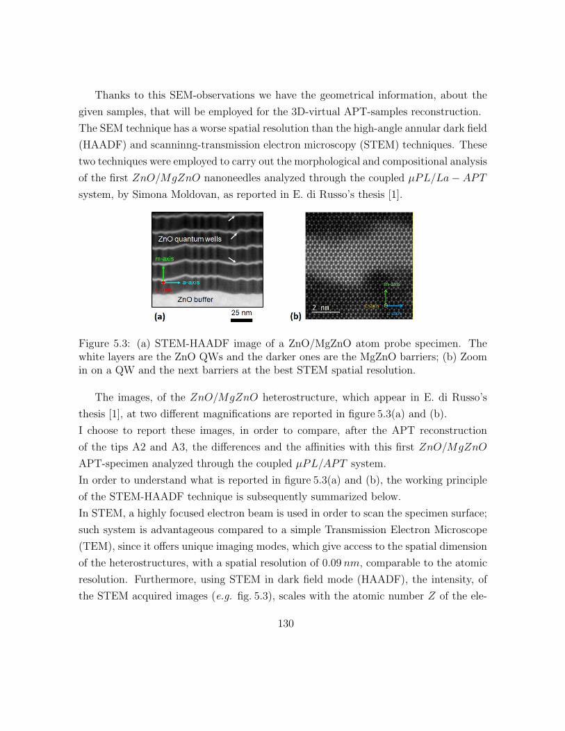
Thanks to this SEM-observations we have the geometrical information, about the
given samples, that will be employed for the 3D-virtual APT-samples reconstruction.
The SEM technique has a worse spatial resolution than the high-angle annular dark field
(HAADF) and scanninng-transmission electron microscopy (STEM) techniques. These
two techniques were employed to carry out the morphological and compositional analysis
of the first ZnO/MgZnO nanoneedles analyzed through the coupled µPL/La− APT
system, by Simona Moldovan, as reported in E. di Russo’s thesis [1].
Figure 5.3: (a) STEM-HAADF image of a ZnO/MgZnO atom probe specimen. Thewhite layers are the ZnO QWs and the darker ones are the MgZnO barriers; (b) Zoomin on a QW and the next barriers at the best STEM spatial resolution.
The images, of the ZnO/MgZnO heterostructure, which appear in E. di Russo’s
thesis [1], at two different magnifications are reported in figure 5.3(a) and (b).
I choose to report these images, in order to compare, after the APT reconstruction
of the tips A2 and A3, the differences and the affinities with this first ZnO/MgZnO
APT-specimen analyzed through the coupled µPL/APT system.
In order to understand what is reported in figure 5.3(a) and (b), the working principle
of the STEM-HAADF technique is subsequently summarized below.
In STEM, a highly focused electron beam is used in order to scan the specimen surface;
such system is advantageous compared to a simple Transmission Electron Microscope
(TEM), since it offers unique imaging modes, which give access to the spatial dimension
of the heterostructures, with a spatial resolution of 0.09 nm, comparable to the atomic
resolution. Furthermore, using STEM in dark field mode (HAADF), the intensity, of
the STEM acquired images (e.g. fig. 5.3), scales with the atomic number Z of the ele-
130

ments within the specimen. Indeed, in HAADF mode, only electrons scattered at high
angles (≈ 30 mrad) are collected by an annular detector and no diffracted electrons
and the images are formed by the elastically scattered electrons which have passed very
close to the atomic nuclei (Z) of the specimen. In this way, the HAADF-STEM images
are not affected by diffraction and high resolution structural information is obtained,
allowing to distinguish between regions where the Mg atoms replace the Zn atoms in
the ZnO ordered lattice, formingMgxZn1−xO alloy. TheMgxZn1−xO barrier is darker
than ZnO and the different shades of darkness related to the MgxZn1−xO alloy can be
observed as a function of the Mg II-site fraction in it. Summing up, the decreasing of
Mg II-site fraction in the MgxZn1−xO alloy increases the HAADF intensity.
The composition profile within the MgZnO barriers is not uniform, figure 5.3, and in
particularMg-depleted or enriched regions along the a-plane are pointed out by the cor-
responding HAADF contrast. The high resolution-STEM-HAADF images, figures 5.3,
reveal that the ZnO buffer used for the growth of that sample does not have a flat
interface, but it shows an irregular V-groove grating profile and the same morphology
is preserved by all the layers grown on this ZnO buffer. The V-groove grating profile
of ZnO-QWs, along the m-axis, was explained by Matsui et al. [151, 165] in terms of
the inhibition of interlayer transport due to a strong step-edge barrier. As shown in
figure 5.3(b), no interdiffusion or other effects leading to compositional gradients are
visible across the interface between the ZnO-QWs and the MgZnO-barriers.
Due to the different adatom diffusion during growth along the c- and a-axis in the plane
of layers, a spatially coherent corrugation develops starting from the bottom contact
layer up to the cap layer. The MgZnO segregation regions, outlined by the HAADF
vertically different dark intensity shades, which occur below the minima of the V-groove
grating profile, are due to compositional inhomogeneities rather than the non-uniform
strain states, as demonstrated by E. di Russo et al. [166]. TheMg-II site fraction varies
by ±10% in absolute values at the bottom and the top of the corrugations. In partic-
ular, the Mg nominal barrier thickness is of tbarr = 15 nm and looking at figure 5.3,
within the MgxZn1−xO barriers, the darkest lines, which occur in correspondence with
top groove edges, are the enriched Mg-regions (x = 0.4), while the regions with bright-
est contrast are found in correspondence with bottom groove edges and they indicate
131

the Mg depleted regions (x = 0.3). The values of the different Mg-concentrations
were, also in that case, evaluated and confirmed, subsequently, by the complementary
APT/µPL reconstruction analysis [167].
In the next sections, the collection and elaboration of the data, by the coupled “in-situ”
µPL/La − APT” system, is reported and finally the results obtained for the tips A2
and A3 are discussed.
5.2 The in-situ µPL/La-APT analysis
The working principle of the coupled microphotoluminescence and the tomographic
atom probe instrument were widely introduced in Chapter 1. The challenging idea
of the “in-situ” approach allows to strictly correlate the variation of the PL signal
with nano-metric scale volumes of the tip evaporated during the APT analysis. This
method opens new perspectives for the study of optical properties of the semiconductor
specimens probed, since it presents more advantages than a simple µPL setup. For
instance:
• differently by commom µPL analysis, the optical emission of single nano-objects,
which are present in the APT-specimen, can be distinguished, since the APT
analysis is based on the evaporation of the radiative centers which compose the
specimen, layer by layer, particle by particle;
• with the coupled“in-situ”La-APT/µPL system a better spatial resolution (<100nm)
than the µPL spectroscopy (∼ λ2) can be obtained;
• the coupled “in-situ” La-APT/µPL system allows correlating the PL emission
with both morphology and composition of the specimen.
In the following sections, I will discuss about:
• the µPL/APT protocol;
• the analysis of the collected data.
132

The µPL/APT protocol is a method which allows to minimize the operation of manipu-
lation of the specimen, since µPL and APT experiments are performed simultaneously.
The data collected, following this protocol, correlate the optical and structural proper-
ties of the probed specimens. In order to yield the 3D sample reconstruction, the mass
spectra, time-of-flight spectra are obtained by the elaboration of the collected data, as
in standard atom probe experiment, and the change of the physical properties of the
system during the experience, for different values of the VDC bias, are reported.
5.2.1 Protocol for the correlative analyses
The possibility to run the µPL and APT experiments, at the same time and “in situ”,
critically depends on the matching of the experimental parameters, which have to work
for both analyses. Experiments were performed keeping the specimen under ultrahigh
vacuum conditions (p < 10−7 Pa) and at low temperature: Tbase = 80K. The PL setup
is the same one employed for the analysis on the diamond tips, described in Chapter
1 and Chapter 3. The laser wavelength was selected in the UV range, at 260 nm, the
laser repetition frequency at 0.5MHz and the incident power was tuned at 600 µW.
These values allowed to have a good PL signal from the ZnO/MgZnO specimen and
to run, at the same time, APT analysis. As saw for diamond tips, the laser beam waist,
focused by a spherical mirror on the tip specimen, is about 1.5 µm.
The first step, before to begin the coupled µPL and APT experience “in-situ”, is to
assure that the MQWs system is not too damaged by the FIB preparation and so that
the heterostructure-needle preserves most of the optically active region. In order to
check that, the sample is probed by only the laser beam, without any applied bias,
focusing the spot laser on the apex of the APT specimen, where we expect to collect a
signal by the whole heterostructure. The PL signal is collected and analyzed through a
grating spectrometer with 320mm focal length and with the highest spectral resolution
of around 0.5meV, equipped with a nitrogen-cooled CCD camera. Generally, the first
spectrum is acquired selecting the grating density with widest wavelength range, to
be sure to acquire the signal from each component of the heterostructure. The µPL-
spectra, related to the tip A2 and tip A3, are showed in figure 5.4. In both spectra,
133

Figure 5.4: PL signal of tip A2 and A3, ZnO/MgZnO MQW heterostructure, withoutbias.
acquired without any VDC applied bias the dominant peak appears at ≈ 3.36 eV and it
is associated to the radiative recombination of the bulk ZnO substrate, the emission at
≈ 3.44 eV is associated to the recombination of the localized excitons in the ZnO-QWs
and finally the broad peak centered at ≈ 3.51 eV is associated to the MgxZn1−xO bar-
riers. Using the equation (4.2), reported in the section 4.1.1, the average value of the
Mg II-site fraction in MgxZn1−xO barriers can be derived. The Mg-concentration was
found to be: “xMg = (0.08± 0.03)”, such value will be verified and compared with the
results of the APT-analysis. Both spectra show the signals of the three components
peaked around the same average values, meaning that the thickness of the QWs and
the MgxZn1−xO barriers average composition of the tips A2 and A3 is the same one or
really close. Indeed, the two APT-samples were obtained by the same ZnO/MgZnO
heterostructure. Once assured to have a good PL signal from the APT specimen, the
coupled La-APT and µPL experience begins. The APT aquisition data software was
developed by Gerald da Costa, at the University of Rouen. Through this software
is possible to control and to choose the parameters that assist the laser-assisted field
evaporation. In order to recognise the ions of the elements which constitute the given
APT sample and to obtain the final APT 3D-virtual sample reconstruction, the differ-
ent mass/charge [Da] ranges, where the peaks of the related different ions have more
134

probability to fall within, were selected, more details in section 5.2.2.1. In order to start
the evaporation and the detection of the ions from the apex of the APT-specimen, the
positive bias was manually increased, from VDC = 0 kV, at steps of ∆VDC = 0.5 kV.
When the detected impacting ions are of the order of magnitude 105 events, it is as-
sumed that layers of ions by the apex of the tip start to evaporate and the detection
rate is fixed at the optimized selected value: ϕ = 0.0025 ions/pulse. This parameter
can have fluctuations, ϕ = 0.0023÷ 0.0028 ions/pulse, in correspondence of the inter-
face between layers having different evaporation fields and as a function of the depth,
since the geometry of the tip changes. A decreasing of the value of the detection rate
is followed by a decreasing of the magnification of the reconstructed specimen. So, we
choose to keep the detection rate automatically constant by the acquisition software.
The correlated acquisition of the data, through the µPL-APT system, was manually
piloted. Each time that one µPL-spectrum was acquired, ∆t ≈ 120 s, it was noted
down the number of detected ions, respectively: at the beginning and at the end of the
recorded µPL-spectrum by the CCD. In this way, it was possible to follow in real time,
during the layers evaporation, the evolution of the peaks related to the ZnO-MQWs,
the MgZnO-barriers and the ZnO-substrate. The column headers of the table 5.2 out-
line the experimental variables which were recorded, step-by-step, in order to merge, at
the end of the experience, the APT and µPL information.
The experiment was concluded when all the QWs and the barriers of the APT sample
♯ origin ∆tacquisition ♯ atoms ♯ atoms VDC ♯ evaporated Commentsfile (s) beginning end (kV) QWs· · · · · · · · · · · · · · · · · · · · ·...
......
......
......
Table 5.2: Column headers of the collected data during the coupled in-situ µPL-APTexperiment. The table with the complete list of values is reported in Appendix A.
were completely evaporated and the software shows the detection of only zinc and oxyde
events, related to the bulk substrate of the MQW heterostructure.
At the end of the specimen evaporation, the La-APT and µPL data are elaborated
135

separately and then put in correlation in order to merge the optical and structural
information related to the ZnO/MgZnO MQWs system studied. For sake of simpli-
fication, I choose to report, in the next sections, the experimental results related only
to the tip A2, while the experimental results related to the tip A3 are reported in Ap-
pendix B. Indeed, both tips came from the same sample, labeled ‘ZOE179’ and the
results are in good agreement.
5.2.2 Data acquired by the La-APT system
5.2.2.1 Mass spectrum
The ZnO/MgxZn1−xO APT-samples were analyzed along the direction of growth, the
[1100] crystallographic orientation, which corresponds to the m-axis. The mass/charge
ranges were selected at the beginning of the APT acquisition, in order to measure the
compososition of the evaporated sample and to identify each peak in the mass spectrum.
Figure 5.5: The mass spectrum related to the tip A2. The elaboration of the APT-datawas realized by Pradip Dalapati.
In the mass spectrum of the ZnO/MgZnO heterostructure, figure 5.5, peaks of
several ions are grouped in different ranges and we can observe that:
• the isolated peak at 32 Da was interpretated as an overlap of 64Zn2+ and O+2 ;
136

• the peaks within the mass range 39.78-42.10 Da were attributed to ZnO2+ and
Zn2O4+2 ;
• the peaks within the mass range 79.59-84.41 Da were attributed to ZnO+ and
Zn2O2+2 .
The zinc “Zn” has five isotopes: 64Zn2+, 66Zn2+, 67Zn2+, 68Zn2+ and 70Zn2+, while
oxygen “O” has three isotopes: 16O+, 17O+ and 18O+. The relative abundances of70Zn2+ and 17O+, 18O+ are very small (< 0.6 %) so such species are not taken in
account for the APT reconstruction, in the mass spectrum.
As noted above, 64Zn2+ and 16O+ ions have the same mass/charge ratio, so they form
a unique peak at ≈ 32Da. Since the natural abundance of 64Zn2+ zinc isotope is known
to be α64 = 0.483, it is possible to evaluate the total amount of Zn and O atoms, using
the following equations (5.1), (5.2):
NZn = NZn66→68/(1− α64) (5.1)
NO = 2 · (N32 − (1− α64) ·NZn) (5.2)
N32 is the number of events detected at the peak m/n ≈ 32Da. NZn66→68 is associated
to 66Zn2+, 67Zn2+ and 68Zn2+ isotopes. In the equation (5.2) the factor 2 is added,
because each 16O+2 ion is composed by two oxygen atoms.
Within the mass range 31.94-35.20 Da, in figure 5.5, it is possible to calculate the re-
spective total amount of zinc and oxygen. The same method has also been adopted in
the mass range 39.78-42.10 Da and 78.41-88.50 Da.
Furthermore, as reported in E. di Russo’s thesis, it is important to consider that the
DC evaporation field of the tip affects the atomic fractions of the detected ions which
appear in the mass spectrum. The number of Zn+ detected ions are observed to de-
crease when the DC field is increased and the Zn2+ ions don’t compensate them, while
the O+2 are more abundant at high field conditions. For this reason is extremally im-
portant to choose and know with precision the experimental conditions adopted during
the experiment. The charge-state-ratio Zn2+/Zn+ is extracted from the mass spectra
by comparing intensities of Zn2+ and Zn+ ions, respectively, in the 31.94-35.20 amu
137

and 63.85-70.12 amu mass ranges values. The Zn2+/Zn+ ratio was used to evaluate
the effective evaporation field, using the Kingham’s curves, that Kingham’s evaluated
by his post-ionization model, introduced in the section 1.2.8. In the present case, F · kfwas ≈ 15 V/nm for Elaser = 1.2 nJ .
Figure 5.6: Distribution of multiple-ion events associated to the mass spectrum pre-sented in fig 5.5. 87% of the total events is associated to single events, while the re-maining 13% is associated to multi-ions detection.
The multiple-ion events were introduced in the section 1.2.7.4, Chapter 1. These
events can depend on: kind of material, analysis conditions and tip geometry. The
abundance of single events associated to the mass spectrum is ∼ 87%, while ∼ 13%
of the total number of events is associated to multi-ion events. The distribution of
multiple-ion events associated to the mass spectrum are presented in figure 5.6. The
multi-ion events may be numerous and phases with different evaporation fields may
produce multi-ion events. In ZnO, the analysis of multi-ion events is difficult due to
the Zn isotopes, so, many molecular ions and peaks can overlap. Furthermore, some
dissociation reactions can lead to the production of some neutral fragments, which can-
not be detected and so they constitute the loss information. Dissociations processes
can be field-induced phenomena and they can take place very close to the tip surface.
In order to take into account the impact factor of this process on the measured com-
position, Zanuttini et al. studied the dissociation of ZnO2+ ions [168]. They demon-
strate that several dissociation channels exhist for the ZnO2+ ions and they strongly
138

depend by the orientation of the ion with respect to the electric field. The reaction:
ZnO2+ → Zn2+ + O produces a neutral fragment that is not detected at low field
and that becomes post-ionized at higher field, in agreement with the ZnO behavior [1].
Therefore, during the field evaporation process, neutral molecules can be formed and
since they are no charged particles, they constitute a selective loss of atoms which are
no accelerated towards the detector. The study performed by Enrico et al. [167] demon-
strated that, notwithstanding the La-APT technique is not exempt from compositional
biases, accurate site fractions of semiconductors ternary alloys, likes MgxZn1−xO, can
be obtained at low surface field conditions. The experimental results were interpre-
tated using a simple preferential evaporation model, described in ref. [167], which can
be transposed to other semiconductor alloy systems.
5.2.2.2 3D reconstruction
During the APT experiments the applied bias increases slowly in order to counterbal-
ance the effects of the increase of the apex radius. The 3D virtual volume specimen
reconstruction was made applying the “standard reconstruction algorithm”. The ex-
perimental parameters for the reconstruction of the tips A2 and A3 are summarized in
table 5.3.
TIP A2Projection point (m+1) 1.8
F · kf (V/nm) 15Curvature factor 0.8
Detection efficiency 0.4
Table 5.3: Tip A2 parameters given by the APT 3D-reconstruction: projection point,F · kf , curvature factor, detection efficiency.
For both the experiments, the detection rate “ϕ” was kept constant, in order to
have a stable value of the magnification related to the 3D reconstruction. The hitmaps
in figures 5.7 were collected along the whole experiment. In particular, in figure 5.7(a)
the distribution of Zn+ ions looks statistically mostly uniform except for a border side
139

effect. The hitmap in figure 5.7(b) reports the charge state ratio (CSR), section 1.2.8
of Chapter 1, of the Zn2+/Zn+ ions, which shows that the average surface field across
the different regions of the whole APT specimen is quite uniform. Inhomogeneity of
the electric field is highlighted by the bias of the Zn2+/Zn+ ions distribution present
on the border of one side of the CSR hitmap.
Figure 5.7: Hitmaps of: (a) the Zn atomic fractions visualized through detector statis-tics and (b) the Zn2+/Zn+ charge state ratio (CSR).
The reconstruction of the 3D volume of the tip A2, in figure 5.8(a) reports a certain
percentage of the Mg2+ detected ions in blue and another percentage of the Zn1+or2+
detected ions in red.
The values correspond to the average measured composition along the crystal a-axis
and the measured II-site fraction is calculated using the equation (5.3):
x =NMg
NZn +NMg
(5.3)
where NZn and NMg are respectively the number of zinc and magnesium ions detected.
In order to study the MgZnO barriers, a chart of the detected Mg II-site fraction was
computed and the 2D distribution of theMg II-site fraction is reported in figure 5.8(b).
The Mg II-site fraction chart shows that there is not a relevant variation of the Mg
II-site fraction along the a-axis and the m-axis directions, inside the MgZnO barriers.
140

Figure 5.8: (a) 3D volume reconstruction of the tip A2 with both the Mg2+ andZn1+or2+ ions, on the left side, and 3D virtual reconstruction only with the Mg2+ andZn1+ ions, on the right side. (b) 2D-distribution of the Mg II-site fraction, calculatedover a volume of (30× 30× 40) nm3.
5.2.2.3 Mg-concentration profile
The Mg II-site fraction profiles were studied along the:
• m-axis in order to get informations about the average value of the Mg II-site
fraction along all the sample and in order to evaluate the QW thickness, observing
the Mg II-site fraction variation across the QW;
• a-axis in order to investigate theMg II-site fraction fluctuation inside theMgZnO
barriers.
In figure 5.9 is plotted the trend of the Mg II-site fraction detected during the APT-
analysis and it looks quite regular, which means that also the evaporation field is almost
constant. The average Mg II-site fraction along the m-axis, in fig. 5.9, is evaluated to
be more near to 0.086± 0.018, such as generally for the propagation of errors, in order
to evaluate the error it has been used the semidifference related to the values of theMg
II-site fraction oscillations.
141

Figure 5.9: Mg II-site fraction profile measured along the m-axis direction. The minimaare associated to a decreasing of Mg content that is abrupt in the QWs regions.
For convention, we started to enumerate with the lowest index the QW or barrier
closest to the ZnO-substrate and then increasing the indexes of the QWs and barriers,
sequentially, moving towards the tip apex.
In order to study the alloy fluctuation inside the MgZnO barriers, the Mg-profile
along the a-axis was investigated. The profiles, in fig. 5.10, revealed that theMg II-site
fraction is almost constant within the barriers and the average value estimated for each
MgZnO barrier is reported in the table 5.4. Along the m-axis, in correspondence of the
crossing of each ZnO-QW, where the Mg concentration decreases, the FWHM of the
Mg-peak profile fluctuation, fig. 5.11, was evaluated and also in this case the average
values of the thickness of the QWs are reported in table 5.5.
Looking at the data collected in table 5.4, we can observe that, for the tip A2,
the Mg II-site fraction inside the barriers is almost constant and it oscillates around an
average value ≈ (0.088±0.008). Furthermore, also the QWs have not constant thickness
and, in the specific case of the tip A2, the thickness of each QW was estimated and
these values are listed in table 5.5, moving from the first QW towards the last one it is
easy to compare the size of each quantum well with the nearest neighbors and to see
that the QWs increase and decrease their thickness in sequence. TheMg concentration
142
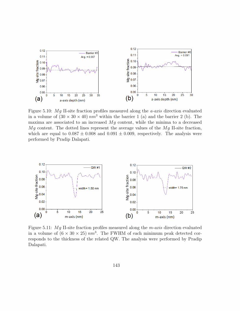
Figure 5.10: Mg II-site fraction profiles measured along the a-axis direction evaluatedin a volume of (30 × 30 × 40) nm3 within the barrier 1 (a) and the barrier 2 (b). Themaxima are associated to an increased Mg content, while the minima to a decreasedMg content. The dotted lines represent the average values of the Mg II-site fraction,which are equal to 0.087 ± 0.008 and 0.091 ± 0.009, respectively. The analysis wereperformed by Pradip Dalapati.
Figure 5.11: Mg II-site fraction profiles measured along the m-axis direction evaluatedin a volume of (6 × 30 × 25) nm3. The FWHM of each minimum peak detected cor-responds to the thickness of the related QW. The analysis were performed by PradipDalapati.
143

Barrier Mg-site fraction♯1 0.087± 0.008♯2 0.085± 0.008♯3 0.087± 0.008♯4 0.087± 0.008♯5 0.089± 0.008♯6 0.091± 0.009♯7 0.088± 0.008
Table 5.4: TheMg II-site fraction evaluated as theprofiles in figure 5.10.
QW FWHM (nm)♯1 1.48± 0.13♯2 1.8± 0.2♯3 1.97± 0.16♯4 2.00± 0.14♯5 2.8± 0.3♯6 2.07± 0.13♯7 2.94± 0.15
Table 5.5: The QWs size, evaluated by the MgII-site fraction profiles in figure 5.11.
evaluated by the APT reconstruction can be compared with the Mg II-site fraction,
deduced by the signal of the MgZnO barrier in the PL spectra related to the tip A2.
5.2.3 µPL analysis
Before introducing the PL experimental results, we remind that the µPL spectroscopy
was carried out on tip A2 and tip A3, illuminated with a UV 260 nm laser focused on
a spot size of ≈ 1µm. The laser repetition rate was 0.5MHz and the laser power was
600µW . The specimens temperature Tbase was kept at 80K. In the next subparagraphs
the data collected and the reported spectra are all referred to the tip A2.
5.2.3.1 Spectra before the evaporation of the sample
The PL spectra in figure 5.4 were acquired at VDC = 0 kV . In these spectra, fig. 5.4,
the signals related to each component of the ZnO/MgZnO heterostructure are present:
the peak of the ZnO substrate is at ≈ 3.36 eV, the signal of the QWs is at ≈ 3.44 eV
and the signal associated to the MgxZn1−xO barriers is at ≈ 3.51 eV. If we compare
the Mg-concentration, xMg = (0.08 ± 0.03), evaluated by the µPL spectrum, without
bias applied, and the Mg-concentration evaluated by the Mg-concentration profile,
xMg = (0.088± 0.025), in the 3D-APT reconstruction, we can conclude that these two
values are consistent.
For the tip A2, the evaporation flux corresponding to a detection rate of ϕ =
144

Figure 5.12: PL spectra collected at the beginning of the “in-situ” µPL-APT analysis.The blue curve is the signal of the tip A2, probed without bias and the dotted blue lineis referred to the tip A2 at the beginning of the evaporation (VDC = 7.5 kV).
0.0025 ions/pulse started at VDC = 7.5kV and the PL-spectrum acquired at this VDC
bias corresponds to the dotted curve, in figure 5.12. The two spectra reported in fig-
ure 5.12, respectively at VDC = 0kV and VDC = 7.5kV were normalized at the same
integration time and, as we can observe, the spectrum acquired at VDC = 7.5kV shows
red-shift (∆E = 15meV) of the signals related to the MgZnO barriers. This behavior
should be related to the effect of the hydrostatic tensile stress on the apex of the APT-
tip induced by the applied high electric field (≈ 10 ÷ 100 V/nm), as demonstrated in
ref. [57]. In order to verify this hypothesis, it is important to look at the trend of all the
spectra during the analysis of the tip. Differently from the peaks related to the barriers
and the ZnO substrate, the signal related to the ZnO QWs increases its intensity at
the beginning of the evaporation process. In the next section, the evolution of the PL
signal is carried forward until the complete evaporation of the heterostructure.
5.2.3.2 Spectra during the evaporation of the sample
Once the evaporation of the APT-specimen begins, the detection rate is fixed at ϕ =
0.0025 ions/pulse and the VDC bias is automatically balanced by the APT software, in
145

order to keep constant the selected detection rate value.
The spectra reported in figure 5.13 show the optical signature related to the components
which constitute the tip A2, during the ongoing evaporation process. Each spectrum
(Si) was collected at the same integration time (∆tacquisition = 150 s) and at the end of
the acquisition of one PL spectrum a new one was acquired.
The spectra reported in figure 5.13 show the trend of all the components present in the
Figure 5.13: Series of spectra, detected during the µPL-APT analysis of the tip A2,where the spectral components progressively disappear due to the evaporation of thetip.
ZnO/MgZnO heterostructure from the beginning of the evaporation process (pointed
out by the green spectrum, labeled as ‘Begin’) until the end of the evaporation of the
last barrier of the ZnO/MgZnO heterostructure (pointed out by the red spectrum,
labeled as ‘End’). As we can observe, the evolution of the signals related to the barriers
and the ZnO substrate show again a clear shift of their peaks towards lower energy, in
agreement with the red-shift observed, for theMgZnO-barrier peak, in the spectra 5.12,
from VDC = 0 kV to VDC = 7.5 kV . During the evaporation of the APT specimen,
figure 5.13, also the signal related to the QWs shows a shift towards lower energy,
but, as already observed in figure 5.12, the intensity of the QWs peak increases and
decreases during the ongoing evaporation from a QW to the next one. This behavior
is supposed to be related either to the specific position of the evaporated QW inside
the nanoneedle or to the shape of the APT-specimen, on which depend the direction
146

of the emitted light, that can be more or less efficiently collected by the spectrometer,
giving spectra of different intensity. Anyway, the present assumption needs additional
experimental proofs. The modifications in the spectral series may be investigated by
direct comparison of different spectra, as reported in figure 5.13, but also by defining
differential spectra ∆Si,i+1 = Si −Si+1, which is particularly useful in the present case,
as shown by the 2D map in figure 5.14(a). The 2D maps in figure 5.14 have reported on
Figure 5.14: Differential spectra represented in a 2D color-map. (a) The red-shift ofthe signals related to the QWs and barriers are highlighted by the two yellow lines. (b)The optical signatures of 1 over 4 QWs are highlighted by the blue circles.
the ordinate-axis the index related to the spectrum S(i) considered and on the abscissa-
axis the emission photon energy, associated to each component of the ZnO/MgZnO
heterostructure. The two yellow diagonal lines, which appear in the 2D map, fig. 5.14(a),
highlight the red-shift of:
• the barriers ∆E ≈ [3.455; 3.51]eV;
• one QW signal ∆E ≈ [3.41; 3.43]eV;
during the acquisition from the spectrum ♯20 until the spectrum ♯60 along the ongoing
evaporation of the sample. While, in figure 5.14(b), the differential emission signals
related to different QWs are circled. Each QW starts to emit at a different energy
position, which depends on its thickness and the related excitonic transition. If we
147

look at the signal of each QW, inside each circle, in figure 5.14(b), a red-shift of the
QW, during the evaporation process is observed. The possibility to distinguish the
signal of neighboring QWs asks a spatial resolution that overlaps the µPL diffraction
limit (laser spot size ≈ 1µm), since, as estimated above, each QW is separated by a
barrier in the tip A2 with approximately constant thickness tbarrier ≈ 45 nm. These
data are better clarified in the next section, correlating the µPL results with the APT
3D-reconstruction of the sample.
5.3 Interpretation of the correlated results
The notes written down, during the analysis protocol, were used to perform a corrected
correlation of the experimental results.
The plots in figure 5.15 completely summarize the results that derive by the correla-
tion of the elaborated data. In figure 5.15(a) are reported two PL spectra which were
acquired respectively: at the beginning of the µPL analysis, labeled as ‘S(0)’, since it
is acquired without any bias, and then the spectrum ‘S(58)’ which was acquired after
the evaporation of the QW♯1 or the beginning of the barrier♯1, which are the closest
to the ZnO substrate. Comparing the spectra S(0) and S(58), the signals of the ZnO
substrate, peaked at E ≈ 3.36 eV, and the MgZnO barrier, peaked at E ≈ 3.51 eV,
show both a similar energy red-shift of −30 meV and −33 meV, respectively, that is
supposed to be related to the effect of the induced tensile uniaxial stress, as it will be
proven in the next subsection. Between the ZnO and MgZnO peaks, the spectrum
‘S(0)’ shows also the signal related to the QWs, while in the spectrum ‘S(58)’ the QW
signal disappear, since they were all evaporated, in agreement with the correlated in-
formation given by the APT-data.
In fig. 5.15(b), the 2D color map is a different representation of the complete serie of
collected µPL spectra reported in figure 5.13, where also the signal related to the QWs
is clearly distinguishable, as much as the signal of the MgZnO barriers and the ZnO
substrate. Thanks to the direct color contrast, to follow the changement of intensity
of the different components during the evaporation is easier. The series of µPL spec-
tra clearly shows, from the top to the bottom of the 2D color map, the progressive
148

bleanching of the spectral components relative to the Mg0.07Zn0.93O barriers and the
QWs.
Figure 5.15: (a) µPL spectra collected at the beginning of the experiment S(0) andafter the evaporation of the last quantum well S(58). The spectral contributions deriveby the ZnO substrate, the QWs and by the MgZnO barriers. (b) Complete serie ofcollected µPL spectra; (c) 3D-reconstruction of the position of Mg atoms and (d) 2D-distribution of the Mg II-site fraction, calculeted over a volume of (30× 30× 40) nm3.The red dashed lines indicate the approximate position of the specimen surface duringthe acquisition of the i − th spectrum. The separation between neighboring QWs isaround 45 nm.
We have concluded the previous section 5.2.3.2 affirming that the optical signature
of the QWs, which appear in the 2D map, figure 5.14, highlighted by blue circles, shift
their emission energies respect to each other, because the recombination energy of each
QW depends only by its own thickness, in non-polar systems. Here, comparing the
index of the spectrum which appears in the 2D map, fig. 5.14(b), and the position of
the specimen surface, corresponding to a set of specific spectrum indeces, reported as
a dashed red line in fig. 5.15(c), the relationship between the QWs signal position in
149

the 2D map, fig. 5.14(b), and their morphology, reconstructed by the APT-data, in
fig. 5.15(c) and (d), is showed to be strictly related. In the table 5.4, the thickness of
each reconstructed QW is reported. Comparing the 2D map, fig. 5.14(b), and the APT
3D-reconstruction, fig. 5.15(c), we can associate to each circle a QW in a precise position
inside the specimen. In particular, the circles in the 2D map highlight the signatures
of the QW♯1 to♯4 and the average emission energy that is possible to associate to each
QW is in good agreement with the evaluated QW thickness, reported in the table 5.4.
It is important to underline again that the interwell distance is as low as 45 nm. The
µPL − APT can thus discriminate the emission of two quantum light emitters that
are much closer than the diffraction limit of the laser wavelength (≈ 1 µm), increasing
in a considerable way the spatial resolution of the simple µPL system. Furthermore
the value of 45 nm distance is dictated only by the specific interwell distance in the
analyzed sample, so, decreasing the distance between two emitters inside the specimen,
probably, a better spatial resolution can be achieved, until the spectral peaks related
the two emitters do not overlap.
5.3.1 Evaluation of the stress using the bandgap deformation
potential associated to the ZnO substrate
The ZnO/MgZnO nanoneedle is an heterostructure composed by semiconductive ma-
terials, so the straight correlation between the observed red-shift and the uniaxial tensile
stress, induced by the high bias applied, needs a brief explanation. In Chapter 3, in
agreement with what several experimental results demonstrated, we have proved that
a dielectric tip, as diamond nanoneedles, under a high electric field (≈ 10 V/nm) can
act as a conductive material, screening the electric field at its surface. In this way, the
electric field, that acts on the surface of the tip, generates a hydrostatic tensile stress
on the apex of the specimen, as reported in the equation (5.4).
σapex =1
2ǫ0F
2s (5.4)
150

This hydrostatic stress at the apex, gradually translates in a uniaxial stress further
from the apex [16, 57]. As demonstrated through the analysis on diamond nanoneedles,
the intensity of the stress is proportional to the inverse cross section of the tip at the
position where the emitter is located, since the mechanical tension is conservative along
the axis of the tip. In an evaporating conical tip, with shank angle α, the apex radius
Rapex linearly increases with the analyzed depth ‘z’, as reported in equation (5.5):
R(z) = R(0) + z · tan(α) (5.5)
where at z = 0 we set as the apex of the tip, at the beginning of the analysis. As
confirmed by the charge-state-ratio of the (Zn2+/Zn+) ions detected by the APT anal-
ysis, the electric field, FS, can be assumed nearly constant, so, in agreement with the
relationship eq.(5.4) also the hydrostatic stress at the apex of the tip can be considered
as constant. The uniaxial stress at depth z generated by the field acting on the tip
apex at the coordinate z evolves as in equation 5.6:
σ(z, z) = σ(z)
(
R(z)
R(z)
)2
(5.6)
where the term z indicates a position along the axis of the tip that is conventionally
fixed. In agreement with the results obtained by diamond nanoneedles and published
in the articles [57, 115], then the µPL-APT system can be used in order to perform
optical piezo-spectroscopy of optically active specimens with a nanometric tip shape.
In particular, once that the light emitter is localized, its photoemission signal can be
used in order to measure the stress in real time, if its behavior under stress or strain is
known. In this case, through all the components which constitute the ZnO/MgZnO
heterostructure, the bulk ZnO is the only one for which the elastic constants and the
deformation potentials are known [149]. So, we can try to evaluate the uniaxial stress
acting in a precise position of the tip, on the ZnO substrate, and to compare the
result obtained with the red-shift observed in the corresponding PL spectrum. As we
can observe, looking at the spectra in fig. 5.15(a), the signal of the ZnO buffer is a
broad peak and in the spectrum ‘S(58)’ doesn’t look well peaked on a precise emission
151

energy position. The reason of such behavior can be explained considering that the
laser spot size is ≈ 1 − 2 µm, so the PL signal is collected by the whole tip, along
all the experiment. Then, the emitting parts of ZnO closest to the tip apex generate
the low-energy shoulder signal, while the parts further from the apex remain nearly
unperturbed, emitting the characteristic ZnO bulk signal. The plot in figure 5.16(b)
reports the trend of the applied DC voltage VDC as a function of the analyzed depth,
and thanks to the equation (5.7):
R(VDC) =VDC
(kf · FS)(5.7)
where the geometric factor kf and the electric field FS are given by the APT 3D re-
construction, the evolution of the apex radius during the evaporation of the tip, can be
also plotted as a function of the depth. The radius seems to increase roughly linearly
as a function of the analyzed depth. The linear increase of the radius with the analyzed
depth was taken into account in order to calculate the uniaxial stress at z = 356 nm,
the depth that corresponds to the interface between the MgZnO barrier and the ZnO
buffer and to compare it with the one observed by the red-shift of the ZnO peak in the
spectrum ‘S(58)’.
The stress was:
1. inferred by the PL experiments;
2. evaluated by the reconstruction parameters, related to ZnO wz-crystal structure
reported in table 4.3, using the relationship between the PL energy shift of the
exciton types involved in the transitions, which are linearly dependent on the
uniaxial strain ǫzz along the z-axis, as reported in ref. [160, 169]
As we can observe in fig. 5.16(b) the values of the uniaxial stress, calculated as in the
case (1) and (2) are in fair agreement, but do not perfectly overlap.
The discrepancies can be explained considering that:
1. the shoulder signal of ZnO buffer can be generated by a portion of the substrate
that lies at larger depth which can explain why the experimental stress results
lower at the beginning of the analysis;
152

Figure 5.16: Study of the effect of the field-induced stress on the PL emission of theZnO substrate. (a) Evolution of the DC voltage applied to the tip during the APTanalysis. A linear trend curve (dashed line) is superimposed to the experimental data.In the inset the location of the reconstructed heterostructure and of the ZnO substrateare shown. (b) Evolution of the spectral shift of the ZnO peak versus the analyzeddepth of the specimen. The experimental values are compared to the expected valuesof the stress at the tip apex and at z = 365 nm, interface between ZnO substrate andthe MgZnO barrier.
2. as an additional hydrostatic stress contribution to the uniaxial stress, as the the
apex surface comes closer to the ZnO interface, generating a larger red-shift than
a pure uniaxial stress. This should explain why the slope of the curve of the PL
signal as a function of the depth, gradually increases for z > 250 nm.
These results proof that through the µPL-APT system is possible to estimate the stress
or strain of a specific portion of the tip during the APT analysis, as for conductive as
for non-conductive specimens.
Finally, we can observe that the shift of the ZnO peak (−30 meV) with that of the
MgZnO alloy (−33meV) are comparable. Althought these two phasees are not located
at the same depth in the APT tip, the PL spectrum ‘S(58)’ is contiguous in the ZnO
substrate. It can be qualitatively concluded that the deformation potentials in the
Mg0.07Zn0.93O alloy does not differ too much by those of bulk ZnO, at least in those
involved in the observed red-shift along the [1100] direction.
153

Conclusions
In this thesis the coupled “in-situ” La-APT/µPL technique was used in order to study
the optical properties related to two different material systems:
1. diamond needle crystals with nanometric apex radius and different color centers;
2. specimens based on ZnO/(Mg,Zn)O MQWs heterostructures.
In order to get access to the optical information of these two different systems, the
different mechanisms which generate the photoemitted signal in the two materials,
under high electric field, are taken into account.
In the case of diamond nanoscale needles, the “in-situ” La-APT/µPL technique was
used to study the radiative transitions of the excited color centers, allowing to attain a
threefold goal:
- the measurement of stress in a nanoscale tip;
- the demonstration of contactless piezo-spectroscopy in nanoscale systems under
uniaxial tensile stress;
- the measurement of the electrostatic field at the surface of a nanometric diamond
needle.
The APT is not used as a nano-analysis tool but rather as a position sensor for the
laser spot in order to focus it on the diamond needle crystal.
For what concerns the analysis of the ZnO/(Mg,Zn)O heterostructure, the “in-situ”
154

optical spectroscopy (µPL) within an atom probe (APT) allows resolving spectral sig-
natures of single quantum emitters with a spatial resolution better than the µPL diffrac-
tion limit. Such signatures can then be correlated with their 3D reconstructed map of
chemical composition, and the effect of uniaxial stress can be assessed.
The potential of the “in-situ” La-APT/µPL technique is enhanced by the possibility to
use it in order to get access to the optical properties of different emitting systems. For
what concerns the diamond needle crystals, the application of a high electrostatic field,
at the apex of these tips, induces an energy splitting of the photoluminescence lines of
color centers. The trend of the energy splitting of the ZPL of the NV0 color center was
found to scale with the square of the voltage applied to the needle, which we interpreted
as due to the electrostatic stress developed as a consequence of the interaction between
the free holes accumulating at the needle apex and the applied field. The diamond
nanotips, probed in this way, have also been scanned along the z-axis (length of the
tip), which corresponds to the <001> crystal direction, from the apex position until
∼ 25 µm toward the base. Furthermore, applying the DC bias of 16 kV, in a region
close to the apex of the tips, it was possible to perform polarization-resolved analysis
of the NV0 peaks. This stress, hydrostatic at the very needle apex, rapidly evolves to
a uniaxial tensile stress along the needle shank. Stresses up to 7 GPa could be esti-
mated accordingly to the model in the proximity of the needle apex. This study consti-
tutes the first experimental quantitative, contactless assessment of the stress building
up inside a field emitter as a consequence of the application of a high voltage at its
apex. The results obtained for diamond should be reproducible for any material or
nanoscale system exhibiting a stress-dependent optical signature: color centers in other
ionic crystals, quantum dots, quantum wells and near band-edge emissions in ultra-high
crystalline quality semiconductor nanowires should exhibit stress-related modifications
of their spectral properties. Such possibilities are also interesting in view of nanoscale
piezospectroscopic studies exploiting the stress field as a parameter for the investiga-
tion of the symmetries of the optically active electron states, which could yield original
information in the domain of quantum cryptography and information. In this study the
symmetry of the NV0 center was confirmed by piezo-spectroscopic polarization-resolved
analysis, through µPL.
155

These results suggest that field-emission tip specimens with known mechanical and ge-
ometrical parameters could be used as optical sensors of intense electrostatic field in
scanning probe microscopes. Furthermore, these experiments provided a validation of
the model according to which the surface of dielectric needle specimens metallized under
high positive fields because free holes accumulate at the apex surface, providing efficient
screening of the applied field and preventing from its penetration in the interior of the
material. The contactless piezo-spectroscopy was performed also on the color center
at 2.65 eV, in order to prove that this color center could be also a better candidate
than the NV0 for the fabrication of strain mediated coupling systems. By contactless
piezo-spectroscopy the strain sensitivity of this color center is compared with that of
the NV0 center. The energy splitting of the center at 2.65 eV was also found scaling
linearly with the uniaxial tensile stress along the <001> direction. At the same value
of stress, the energy splitting of the center at 2.65 eV is twice than the one of NV0.
Polarization-resolved µPL measurements of the 2.65 eV center, for diamond tips with
crystal axis along the <001> crystalline direction, were also performed, under strain
field. Despite the complete polarization-resolved PL study, the symmetry of this color
center does not correspond to anyone reported in the literature. So, regarding the sym-
metry of the 2.65 eV center, further studies are needed in order understand its nature.
These measurents on the NV0 and 2.65 eV center were performed in the UV range of
exciting wavelength. Piezo-spectroscopic studies in the IR-range on the 2.65 eV color
center could open more interesting perspectives about the application of this color cen-
ter as stress-field sensor. Finally, preliminary findings about the temporal dynamic of
the recombination process assessed through TRPL shown that the decay time of the
NV0 centers seems to decrease from the apex of the diamond tip towards its base and
also as a function of the induced stress. Anyway, further studies are needed.
The analysis performed on the ZnO/(Mg,Zn)O through the in-situ µPL-APT system
were used to correlate the APT 3D-reconstruction and the PL emission, to evaluate the
Mg II-site fraction “xMg = 0.07” by the position of the peak related to the MgZnO in
the PL spectrum and to attribute an average emission energy to each QW, making the
coupled µPL-APT a super-resolution technique with a spatial resolution of ≈ 45 nm,
where such distance is related just to the interwell distance of the specimen analyzed.
156

It is reasonable to think that in futher studies this spatial resolution can decrease the
scale, if the interwell distance between the two emitters decreases and their signal do
not significantly overlaps. The µPL data related to the ZnO/MgZnO heterostructure
were used to measure the stress in real time for a specific depth, provided that, by the
correlation with the APT-analysis, the light emitter is localized and its behavior under
stress or strain is known. In particular, the attention was focused on the emission from
the ZnO, for which the deformation potentials were known from past works in litera-
ture [149], in order to use them to infer the stress with the PL spectral shift of the ZnO
peak. The uniaxial stress was calculated at the depth of the interface between the ZnO
substrate and the MgZnO barrier. Although these two phases are not located at the
same depth, the portion of barrier producing the PL signal, at the depth corresponding
to their interface, is contiguous to the ZnO substrate, and the stress experienced by
it should not be too different. It can be qualitatively concluded that the deformation
potentials in Mg0.07Zn0.93O should not differ too much from those of ZnO, at least in
those involved in the red shift for uniaxial stress along the length-axial direction of the
tip, which corresponds to the [1100] direction.
The study of polarization-dependence near-band-edge PL transition in ZnO strain-free
nanowires is known by literature [170] and it is in agreement with the symmetry of the
excitonic transitions in wurtzite semiconductor crystals, as reported in ref. [171]. Going
further, polarization-resolved µPL measurements of the ZnO/MgZnO heterostructure,
under strain-field could be a new and interesting study in order to discover if the in-
duced stress-field changes the symmetry of the excitonic transitions related to the ZnO
QWs and the MgZnO barriers.
157

Bibliography
[1] E. Di Russo, Study of the physical mechanisms leading to compositional biases
in atom probe tomography of semiconductors. These de doctorat, Universite de
Rouen, 2018.
[2] D. Bluvstein, Z. Zhang, and A. C. B. Jayich, “Identifying and Mitigating Charge
Instabilities in Shallow Diamond Nitrogen-Vacancy Centers,”Physical Review Let-
ters, vol. 122, p. 076101, Feb. 2019.
[3] G. Davies and M. F. Hamer, “Optical studies of the 1.945 eV vibronic band
in diamond,” Proceedings of the Royal Society A: Mathematical, Physical and
Engineering Sciences, vol. 348, no. 1653, pp. 285–298, 1976.
[4] G. Davies, C. Foy, and K. O\textbackslashtextquotesingleDonnell, “The TR12
vibronic band in diamond,” vol. 14, no. 28, pp. 4153–4165.
[5] K. Iakoubovskii and G. J. Adriaenssens, “Optical study of some interstitial-related
centres in CVD diamond,” vol. 181, no. 1, pp. 59–64.
[6] K. Iakoubovskii, G. Adriaenssens, N. Dogadkin, and A. Shiryaev, “Optical charac-
terization of some irradiation-induced centers in diamond,” vol. 10, no. 1, pp. 18–
26.
[7] F. J. McClung and R. W. Hellwarth, “Giant Optical Pulsations from Ruby,”
Journal of Applied Physics, vol. 33, pp. 828–829, Mar. 1962.
[8] G. Smith, “The early laser years at Hughes Aircraft Company,” IEEE Journal of
Quantum Electronics, vol. 20, pp. 577–584, June 1984.
158

[9] W. E. Lamb, “Theory of an Optical Maser,”Physical Review, vol. 134, pp. A1429–
A1450, June 1964.
[10] L. E. Hargrove, R. L. Fork, and M. A. Pollack, “Locking of He-Ne Laser Modes
Induced by Synchronous Intracavity Modulation,”Applied Physics Letters, vol. 5,
pp. 4–5, July 1964.
[11] L. Porres, A. Holland, L.-O. Palsson, A. P. Monkman, C. Kemp, and A. Beeby,
“Absolute measurements of photoluminescence quantum yields of solutions using
an integrating sphere,” Journal of Fluorescence, vol. 16, pp. 267–272, Mar. 2006.
[12] A. R. Henderson, “Fabry-Perot interferometers. G. Hernandez,” Optics Laser
Technology, vol. 18, pp. 274–274, Oct. 1986.
[13] C. Kammerer, G. Cassabois, C. Voisin, M. Perrin, C. Delalande, P. Roussignol,
and J. M. Gerard, “Interferometric correlation spectroscopy in single quantum
dots,”Applied Physics Letters, vol. 81, pp. 2737–2739, Sept. 2002.
[14] R. Bell, “Introductory Fourier Transform Spectroscopy - 1st Edition,” Dec. 2012.
[15] V. F. Lefebvre W. and S. X., Atom Probe Tomography: Put Theory Into Practice.
Academic Press, May 2016.
[16] E. P. Silaeva, L. Arnoldi, M. L. Karahka, B. Deconihout, A. Menand, H. J.
Kreuzer, and A. Vella, “Do Dielectric Nanostructures Turn Metallic in High-
Electric dc Fields?,”Nano Letters, vol. 14, pp. 6066–6072, Nov. 2014.
[17] E. P. Silaeva, J. Houard, A. Hideur, G. Martel, and A. Vella, “Field evaporation of
semiconductors assisted by nonequilibrium phonon excitations,” Physical Review
B, vol. 92, p. 195307, Nov. 2015.
[18] L. J. Lauhon, P. Adusumilli, P. Ronsheim, P. L. Flaitz, and D. Lawrence, “Atom-
Probe Tomography of Semiconductor Materials and Device Structures,” MRS
Bulletin, vol. 34, pp. 738–743, Oct. 2009.
159
[19] C. Oberdorfer, P. Stender, C. Reinke, and G. Schmitz, “Laser-Assisted Atom
Probe Tomography of Oxide Materials,” Microscopy and Microanalysis, vol. 13,
pp. 342–346, Oct. 2007.
[20] K. Thompson, R. Alvis, and D. Lawerence, “IBM: P. Ronsheim, P. Flaitz, J.
McMurray, C. Molella, C. Parks,” p. 24, 2006.
[21] E. W. MAŒller and K. Bahadur,“Field Ionization of Gases at a Metal Surface and
the Resolution of the Field Ion Microscope,” Physical Review, vol. 102, pp. 624–
631, May 1956.
[22] E. R. McMullen and J. P. Perdew, “Theory of field evaporation of the surface
layer in jellium and other metals,” Physical Review B, vol. 36, pp. 2598–2606,
Aug. 1987.
[23] E. R. McMullen, J. P. Perdew, and J. H. Rose, “Effects of an intense electric field
on metal surface geometry,” Solid State Communications, vol. 44, pp. 945–949,
Nov. 1982.
[24] H. J. Kreuzer and K. Nath,“Field evaporation,”Surface Science, vol. 183, pp. 591–
608, May 1987.
[25] F. Vurpillot and C. Oberdorfer, “Modeling Atom Probe Tomography: A review,”
Ultramicroscopy, vol. 159, pp. 202–216, Dec. 2015.
[26] F. Djurabekova, S. Parviainen, A. Pohjonen, and K. Nordlund, “Atomistic mod-
eling of metal surfaces under electric fields: Direct coupling of electric fields to a
molecular dynamics algorithm,”Physical Review E, vol. 83, p. 026704, Feb. 2011.
[27] M. Wada, “On the thermally activated field evaporation of surface atoms,”Surface
Science, vol. 145, pp. 451–465, Oct. 1984.
[28] K. Chibane and R. G. Forbes, “The temperature dependence of evaporation field
for Gomer-type field-evaporation mechanisms,”Surface Science, vol. 122, pp. 191–
215, Nov. 1982.
160

[29] T. F. Kelly, A. Vella, J. H. Bunton, J. Houard, E. P. Silaeva, J. Bogdanowicz, and
W. Vandervorst, “Laser pulsing of field evaporation in atom probe tomography,”
Current Opinion in Solid State and Materials Science, vol. 18, pp. 81–89, Apr.
2014.
[30] A. Sommerfeld, “Mathematische Theorie der Diffraction | SpringerLink.”
[31] A. Vella, “On the interaction of an ultra-fast laser with a nanometric tip by laser
assisted atom probe tomography: a review,”Ultramicroscopy, vol. 132, pp. 5–18,
Sept. 2013.
[32] G.-H. Ding, C. T. Chan, Z. Q. Zhang, and P. Sheng, “Resonance-enhanced optical
annealing of silicon nanowires,”Physical Review B, vol. 71, p. 205302, May 2005.
[33] M. K. Miller, Atom Probe Tomography: Analysis at the Atomic Level. Springer
Science & Business Media, Dec. 2012. Google-Books-ID: E0 aBwAAQBAJ.
[34] A. Cerezo, T. J. Godfrey, C. R. M. Grovenor, M. G. Hetherington, R. M. Hoyley,
J. P. Jakubovics, J. A. Liddle, G. D. W. Smith, and G. M. Worrall, “Materials
analysis with a position-sensitive atom probe,” Journal of Microscopy, vol. 154,
no. 3, pp. 215–225, 1989.
[35] G. Schmitz, “Nanoanalysis by Atom Probe Tomography,” in Nanotechnology,
pp. 213–257, American Cancer Society, 2010.
[36] F. Vurpillot, B. Gault, B. P. Geiser, and D. J. Larson, “Reconstructing atom
probe data: A review,”Ultramicroscopy, vol. 132, pp. 19–30, Sept. 2013.
[37] C. M. C. d. Castilho, “Ion trajectories in atom probe field ion microscopy and gas
field ion sources,” Journal of Physics D: Applied Physics, vol. 32, pp. 2261–2265,
Aug. 1999.
[38] G. Da Costa, F. Vurpillot, A. Bostel, M. Bouet, and B. Deconihout, “Design of
a delay-line position-sensitive detector with improved performance,” Review of
Scientific Instruments, vol. 76, p. 013304, Dec. 2004.
161
[39] Y. C. Chen and D. N. Seidman, “On the atomic resolution of a field ion micro-
scope,” Surface Science, vol. 26, pp. 61–84, June 1971.
[40] B. Gault, M. Muller, A. La Fontaine, M. P. Moody, A. Shariq, A. Cerezo, S. P.
Ringer, and G. D. W. Smith, “Influence of surface migration on the spatial resolu-
tion of pulsed laser atom probe tomography,”Journal of Applied Physics, vol. 108,
p. 044904, Aug. 2010.
[41] M. P. Moody, A. V. Ceguerra, A. J. Breen, X. Y. Cui, B. Gault, L. T. Stephen-
son, R. K. W. Marceau, R. C. Powles, and S. P. Ringer, “Atomically resolved
tomography to directly inform simulations for structure-property relationships,”
Nature Communications, vol. 5, p. 5501, Nov. 2014.
[42] A. R. Waugh, E. D. Boyes, and M. J. Southon, “Investigations of field evaporation
with a field-desorption microscope,” Surface Science, vol. 61, pp. 109–142, Dec.
1976.
[43] M. K. Miller, “THE EFFECTS OF LOCAL MAGNIFICATION AND TRA-
JECTORY ABERRATIONS ON ATOM PROBE ANALYSIS,” Le Journal de
Physique Colloques, vol. 48, pp. C6–565–C6–570, Nov. 1987.
[44] F. Vurpillot, A. Cerezo, D. Blavette, and D. J. Larson, “Modeling Image Distor-
tions in 3dap,”Microscopy and Microanalysis, vol. 10, pp. 384–390, June 2004.
[45] D. J. Larson, B. P. Geiser, T. J. Prosa, S. S. A. Gerstl, D. A. Reinhard, and T. F.
Kelly, “Improvements in planar feature reconstructions in atom probe tomogra-
phy,” Journal of Microscopy, vol. 243, pp. 15–30, July 2011.
[46] N. Rolland, F. Vurpillot, S. Duguay, and D. Blavette, “Dynamic evolution and
fracture of multilayer field emitters in atom probe tomography: a new interpre-
tation,” The European Physical Journal Applied Physics, vol. 72, p. 21001, Nov.
2015.
162

[47] B. Gault, F. d. Geuser, L. T. Stephenson, M. P. Moody, B. C. Muddle, and S. P.
Ringer, “Estimation of the Reconstruction Parameters for Atom Probe Tomogra-
phy,”Microscopy and Microanalysis, vol. 14, pp. 296–305, Aug. 2008.
[48] T. M. Smeeton, M. J. Kappers, J. S. Barnard, M. E. Vickers, and C. J.
Humphreys, “Electron-beam-induced strain within InGaN quantum wells: False
indium “cluster” detection in the transmission electron microscope,” Applied
Physics Letters, vol. 83, pp. 5419–5421, Dec. 2003.
[49] R. Agrawal, R. A. Bernal, D. Isheim, and H. D. Espinosa, “Characterizing
Atomic Composition and Dopant Distribution in Wide Band Gap Semiconduc-
tor Nanowires Using Laser-Assisted Atom Probe Tomography,” The Journal of
Physical Chemistry C, vol. 115, pp. 17688–17694, Sept. 2011.
[50] M. Karahka and H. J. Kreuzer, “Field evaporation of oxides: A theoretical study,”
Ultramicroscopy, vol. 132, pp. 54–59, Sept. 2013.
[51] B. Gault, D. W. Saxey, M. W. Ashton, S. B. Sinnott, A. N. Chiaramonti, M. P.
Moody, and D. K. Schreiber, “Behavior of molecules and molecular ions near a
field emitter,”New Journal of Physics, vol. 18, p. 033031, Mar. 2016.
[52] F. De Geuser, B. Gault, A. Bostel, and F. Vurpillot, “Correlated field evaporation
as seen by atom probe tomography,” Surface Science, vol. 601, no. 2, pp. 536 –
543, 2007.
[53] D. W. Saxey, “Correlated ion analysis and the interpretation of atom probe mass
spectra,”Ultramicroscopy, vol. 111, pp. 473–479, May 2011.
[54] D. R. Kingham, “The post-ionization of field evaporated ions: A theoretical ex-
planation of multiple charge states,” Surface Science, vol. 116, pp. 273–301, Apr.
1982.
[55] A. V. d. A. Neto and C. M. C. d. Castilho, “Some remarks on the Haydock-
Kingham model for field ionization,” Journal of Physics B: Atomic, Molecular
and Optical Physics, vol. 24, pp. 2609–2615, June 1991.
163

[56] Z. Yang, D. Lichtenwalner, A. Morris, J. Krim, and A. I. Kingon, “Contact degra-
dation in hot/cold operation of direct contact micro-switches,” Journal of Mi-
cromechanics and Microengineering, vol. 20, p. 105028, Sept. 2010.
[57] L. Rigutti, L. Venturi, J. Houard, A. Normand, E. P. Silaeva, M. Borz, S. A.
Malykhin, A. N. Obraztsov, and A. Vella, “Optical contactless measurement of
electric field-induced tensile stress in diamond nanoscale needles,” vol. 17, no. 12,
pp. 7401–7409.
[58] E. Di Russo, N. Cherkashin, M. Korytov, A. E. Nikolaev, A. V. Sakharov, A. F.
Tsatsulnikov, B. Bonef, I. Blum, J. Houard, G. Da Costa, D. Blavette, and
L. Rigutti, “Compositional accuracy in atom probe tomography analyses per-
formed on III-N light emitting diodes,” Journal of Applied Physics, vol. 126,
p. 124307, Sept. 2019.
[59] M. K. Miller, K. F. Russell, K. Thompson, R. Alvis, and D. J. Larson, “Re-
view of Atom Probe FIB-Based Specimen Preparation Methods,”Microscopy and
Microanalysis, vol. 13, pp. 428–436, Dec. 2007.
[60] L. Rigutti, A. Vella, F. Vurpillot, A. Gaillard, N. Sevelin-Radiguet, J. Houard,
A. Hideur, G. Martel, G. Jacopin, A. D. Luna Bugallo, and B. Deconihout, “Cou-
pling atom probe tomography and photoluminescence spectroscopy: Exploratory
results and perspectives,”Ultramicroscopy, vol. 132, pp. 75–80, Sept. 2013.
[61] M. K. Miller, “Sculpting Needle-Shaped Atom Probe Specimens with a Dual Beam
FIB,”Microscopy and Microanalysis, vol. 11, pp. 808–809, Aug. 2005.
[62] M. Grundmann, The physics of semiconductors: an introduction including
nanophysics and applications. Graduate texts in physics, Springer-Verlag, 2nd
ed ed., 2010.
[63] J. R. Chelikowsky and S. G. Louie, “First-principles linear combination of atomic
orbitals method for the cohesive and structural properties of solids: Application
to diamond,” Physical Review B, vol. 29, pp. 3470–3481, Mar. 1984.
164

[64] C. D. Clark, P. J. Dean, P. V. Harris, and W. C. Price, “Intrinsic edge absorption
in diamond,”Proceedings of the Royal Society of London. Series A. Mathematical
and Physical Sciences, vol. 277, pp. 312–329, Feb. 1964.
[65] K. Miyoshi, “Structures and mechanical properties of natural and synthetic dia-
monds,” p. 26.
[66] T. S., T. K., P. Patel, F. G., and T. K., “Diamond, diamond-like carbon (DLC)
and diamond-like nanocomposite (DLN) thin films for MEMS applications,” in
Microelectromechanical Systems and Devices (N. Islam, ed.), InTech.
[67] S. B. Singh, M. Pandey, N. Chand, A. Biswas, D. Bhattacharya, S. Dash, A. K.
Tyagi, R. M. Dey, S. K. Kulkarni, and D. S. Patil, “Optical and mechanical
properties of diamond like carbon films deposited by microwave ECR plasma
CVD,” vol. 31, no. 5, pp. 813–818.
[68] P. Hess, “The mechanical properties of various chemical vapor deposition diamond
structures compared to the ideal single crystal,” vol. 111, no. 5, p. 051101.
[69] “The absorption spectra of natural and irradiated diamonds,” vol. 234, no. 1198,
pp. 363–381.
[70] J. Walker, “Optical absorption and luminescence in diamond,” vol. 42, no. 10,
pp. 1605–1659.
[71] J. J. Sinai and S. Y. Wu, “Lattice dynamics of isolated nitrogen in synthetic
diamond,” vol. 43, no. 15, pp. 12419–12424.
[72] R. Ulbricht, S. T. van der Post, J. P. Goss, P. R. Briddon, R. Jones, R. U. A.
Khan, and M. Bonn, “Single substitutional nitrogen defects revealed as electron
acceptor states in diamond using ultrafast spectroscopy,” vol. 84, no. 16.
[73] S. F. Martin, “Methodology for the construction of quaternary carbon centers,”
vol. 36, no. 4, pp. 419–460.
165

[74] V. Blank, M. Popov, G. Pivovarov, N. Lvova, and S. Terentev, “Mechanical prop-
erties of different types of diamond,” vol. 8, no. 8, pp. 1531–1535.
[75] A. T. Collins, “The characterisation of point defects in diamond by luminescence
spectroscopy,” vol. 1, no. 5, pp. 457–469.
[76] A. S. Stepanov, A. V. Korsakov, O. P. Yuryeva, V. A. Nadolinniy, M. Perraki,
K. De Gussem, and P. Vandenabeele, “Brown diamonds from an eclogite xenolith
from udachnaya kimberlite, yakutia, russia,” vol. 80, no. 1, pp. 41–48.
[77] A. M. Zaitsev, Optical Properties of Diamond: A Data Handbook. Springer-Verlag.
[78] J. R. Maze, A. Gali, E. Togan, Y. Chu, A. Trifonov, E. Kaxiras, and M. D.
Lukin, “Properties of nitrogen-vacancy centers in diamond: the group theoretic
approach,” vol. 13, no. 2, p. 025025.
[79] A. N. Obraztsov, P. G. Kopylov, A. L. Chuvilin, and N. V. Savenko, “Production
of single crystal diamond needles by a combination of CVD growth and thermal
oxidation,” vol. 18, no. 10, pp. 1289–1293.
[80] P. G. Kopylov, A. N. Obraztsov, M. A. Dolganov, and S. S. Abramchuk, “Forma-
tion of pyramidal shaped single crystal diamonds in chemical vapor deposition,”
vol. 45, no. 5, pp. 553–557.
[81] A. A. Zolotukhin, M. A. Dolganov, A. M. Alekseev, and A. N. Obraztsov, “Single-
crystal diamond microneedles shaped at growth stage,” vol. 42, pp. 15–20.
[82] A. Zolotukhin, P. G. Kopylov, R. R. Ismagilov, and A. N. Obraztsov, “Thermal
oxidation of CVD diamond,” vol. 19, no. 7, pp. 1007–1011.
[83] M. W. Doherty, N. B. Manson, P. Delaney, F. Jelezko, J. Wrachtrup, and L. C.
Hollenberg, “The nitrogen-vacancy colour centre in diamond,” vol. 528, no. 1,
pp. 1–45.
166

[84] N. B. Manson, J. P. Harrison, and M. J. Sellars, “Nitrogen-vacancy center in
diamond: Model of the electronic structure and associated dynamics,” vol. 74,
no. 10.
[85] H. Sternschulte, K. Thonke, R. Sauer, P. C. MAŒnzinger, and P. Michler,
“1.681-eV luminescence center in chemical-vapor-deposited homoepitaxial dia-
mond films,” vol. 50, no. 19, pp. 14554–14560.
[86] A. Gali and J. R. Maze, “Ab initio study of the split silicon-vacancy defect in
diamond: Electronic structure and related properties,”Physical Review B, vol. 88,
Dec. 2013.
[87] L. J. Rogers, K. D. Jahnke, M. W. Doherty, A. Dietrich, L. P. McGuinness,
C. MAŒller, T. Teraji, H. Sumiya, J. Isoya, N. B. Manson, and F. Jelezko,
“Electronic structure of the negatively charged silicon-vacancy center in diamond,”
vol. 89, no. 23.
[88] S. A. Malykhin, R. R. Ismagilov, F. T. Tuyakova, E. A. Obraztsova, P. V. Fe-
dotov, A. Ermakova, P. Siyushev, K. G. Katamadze, F. Jelezko, Y. P. Rakovich,
and A. N. Obraztsov, “Photoluminescent properties of single crystal diamond
microneedles,” vol. 75, pp. 49–55.
[89] F. T. Tuyakova, E. A. Obraztsova, E. V. Korostylev, D. V. Klinov, K. A.
Prusakov, A. A. Alekseev, R. R. Ismagilov, and A. N. Obraztsov, “Photo- and
cathodo-luminescence of needle-like single crystal diamonds,” vol. 179, pp. 539–
544.
[90] N. Aslam, G. Waldherr, P. Neumann, F. Jelezko, and J. Wrachtrup, “Photo-
induced ionization dynamics of the nitrogen vacancy defect in diamond investi-
gated by single-shot charge state detection,” vol. 15, no. 1, p. 013064.
[91] H. B. Dyer, F. A. Raal, L. Du Preez, and J. H. N. Loubser, “Optical absorption
features associated with paramagnetic nitrogen in diamond,” vol. 11, no. 112,
pp. 763–774.
167

[92] G. Davies, “Dynamic jahn-teller distortions at trigonal optical centres in dia-
mond,” vol. 12, no. 13, pp. 2551–2566.
[93] Y. Mita, “Change of absorption spectra in type-i b diamond with heavy neutron
irradiation,” vol. 53, no. 17, pp. 11360–11364.
[94] H.-Q. Zhao, M. Fujiwara, and S. Takeuchi, “Effect of substrates on the temper-
ature dependence of fluorescence spectra of nitrogen vacancy centers in diamond
nanocrystals,” vol. 51, p. 090110.
[95] N. Manson and J. Harrison, “Photo-ionization of the nitrogen-vacancy center in
diamond,”Diamond and Related Materials, vol. 14, pp. 1705–1710, Oct. 2005.
[96] K. Wang, J. W. Steeds, Z. Li, and Y. Tian, “Photoluminescence studies of both
the neutral and negatively charged nitrogen-vacancy center in diamond,” vol. 22,
no. 1, pp. 108–112.
[97] J. R. Weber, W. F. Koehl, J. B. Varley, A. Janotti, B. B. Buckley, C. G. Van de
Walle, and D. D. Awschalom,“Quantum computing with defects,”vol. 107, no. 19,
pp. 8513–8518.
[98] N. Manson and C. Wei,“Transient hole burning in n-v centre in diamond,”Journal
of Luminescence, vol. 58, pp. 158–160, Jan. 1994.
[99] J. Storteboom, P. Dolan, S. Castelletto, X. Li, and M. Gu, “Lifetime investigation
of single nitrogen vacancy centres in nanodiamonds,”Optics Express, vol. 23, no. 9,
p. 11327, 2015.
[100] F. A. Inam, M. D. W. Grogan, M. Rollings, T. Gaebel, J. M. Say, C. Bradac,
T. A. Birks, W. J. Wadsworth, S. Castelletto, J. R. Rabeau, and M. J. Steel,
“The jahn-teller effect and vibronic coupling at deep levels in diamond,” Reports
on Progress in Physics, vol. 44, pp. 787–830, July 1981.
[101] A. Gali, “Theory of the neutral nitrogen-vacancy center in diamond and its ap-
plication to the realization of a qubit,” Physical Review B, vol. 79, June 2009.
168

[102] F. A. Inam, M. D. W. Grogan, M. Rollings, T. Gaebel, J. M. Say, C. Bradac,
T. A. Birks, W. J. Wadsworth, S. Castelletto, J. R. Rabeau, and M. J. Steel,
“Emission and nonradiative decay of nanodiamond NV centers in a low refractive
index environment,”ACS Nano, vol. 7, no. 5, pp. 3833–3843, 2013.
[103] A. S. Orekhov, F. T. Tuyakova, E. A. Obraztsova, A. B. Loginov, A. L. Chuvilin,
and A. N. Obraztsov, “Structural peculiarities of single crystal diamond needles
of nanometer thickness,”Nanotechnology, vol. 27, p. 455707, Oct. 2016.
[104] A. T. Collins, “The fermi level in diamond,” Journal of Physics: Condensed Mat-
ter, vol. 14, no. 14, p. 3743, 2002.
[105] K. Iakoubovskii, G. J. Adriaenssens, and M. Nesladek, “Photochromism of
vacancy-related centres in diamond,” Journal of Physics: Condensed Matter,
vol. 12, pp. 189–199, Dec. 1999.
[106] Y. Dumeige, F. Treussart, R. Alleaume, T. Gacoin, J.-F. Roch, and P. Grangier,
“Photo-induced creation of nitrogen-related color centers in diamond nanocrystals
under femtosecond illumination,” Journal of Luminescence, vol. 109, pp. 61–67,
Aug. 2004.
[107] K. Iakoubovskii and A. Stesmans, “Chemical vapour deposition diamond studied
by optical and electron spin resonance techniques,”vol. 14, no. 17, pp. R467–R499.
[108] T. T. Tsong, “Field penetration and band bending near semiconductor surfaces
in high electric fields,” vol. 81, no. 1, pp. 28–42.
[109] M. K. Miller, A. Cerezo, M. G. Hetherington, and G. D. W. S. FRS, Atom Probe
Field Ion Microscopy. Monographs on the Physics and Chemistry of Materials,
Oxford University Press.
[110] S. A. Malykhin, J. Houard, R. R. Ismagilov, A. S. Orekhov, A. Vella, and A. N.
Obraztsov, “Luminescent characteristics of needle-like single crystal diamonds,”
vol. 255, no. 1, p. 1700189.
169
[111] P. Tamarat, T. Gaebel, J. R. Rabeau, M. Khan, A. D. Greentree, H. Wilson,
L. C. L. Hollenberg, S. Prawer, P. Hemmer, F. Jelezko, and J. Wrachtrup, “Stark
shift control of single optical centers in diamond,” vol. 97, no. 8, p. 083002.
[112] M. Ruhl, C. Ott, S. Gotzinger, M. Krieger, and H. B. Weber, “Controlled gener-
ation of intrinsic near-infrared color centers in 4h-SiC via proton irradiation and
annealing,”Applied Physics Letters, vol. 113, p. 122102, Sept. 2018.
[113] G. Wolfowicz, C. P. Anderson, A. L. Yeats, S. J. Whiteley, J. Niklas, O. G.
Poluektov, F. J. Heremans, and D. D. Awschalom, “Optical charge state control
of spin defects in 4h-SiC,”Nature Communications, vol. 8, Nov. 2017.
[114] M. Radulaski, M. Widmann, M. Niethammer, J. L. Zhang, S.-Y. Lee, T. Rendler,
K. G. Lagoudakis, N. T. Son, E. Janzen, T. Ohshima, J. Wrachtrup, and J. Vuck-
ovic, “Scalable Quantum Photonics with Single Color Centers in Silicon Carbide,”
Nano Letters, vol. 17, pp. 1782–1786, Mar. 2017.
[115] L. Venturi, L. Rigutti, J. Houard, I. Blum, S. Malykhin, A. Obraztsov, and
A. Vella, “Strain sensitivity and symmetry of 2.65ev color center in diamond
nanoscale needles,” vol. 114, no. 14, p. 143104.
[116] G. Davies, “The effect of nitrogen impurity on the annealing of radiation damage
in diamond,” vol. 5, no. 17, pp. 2534–2542.
[117] K. Mohammed, G. Davies, and A. T. Collins, “Uniaxial stress splitting of photolu-
minescence transitions at optical centres in cubic crystals: theory and application
to diamond,” vol. 15, no. 12, pp. 2779–2788.
[118] M. Albrecht, H. P. Strunk, R. Hull, and J. M. Bonar, “Dislocation glide in 110planes in semiconductors with diamond or zinc-blende structure,” vol. 62, no. 18,
pp. 2206–2208.
[119] L. Pizzagalli, “Stability and mobility of screw dislocations in 4h, 2h and 3c silicon
carbide,” vol. 78, pp. 236–244.
170

[120] D. G. Brandon and M. Wald, “The direct observation of lattice defects by field
ion microscopy,” vol. 6, no. 68, pp. 1035–1044.
[121] J. E. Field and C. S. J. Pickles, “Strength, fracture and friction properties of
diamond,” vol. 5, no. 6, pp. 625–634.
[122] J. Teissier, A. Barfuss, P. Appel, E. Neu, and P. Maletinsky, “Strain coupling of a
nitrogen-vacancy center spin to a diamond mechanical oscillator,” vol. 113, no. 2,
p. 020503.
[123] E. R. MacQuarrie, M. Otten, S. K. Gray, and G. D. Fuchs, “Cooling a mechanical
resonator with nitrogen-vacancy centres using a room temperature excited state
spin-strain interaction,” vol. 8, p. 14358.
[124] K. W. Lee, D. Lee, P. Ovartchaiyapong, J. Minguzzi, J. R. Maze, and A. C.
Bleszynski Jayich, “Strain coupling of a mechanical resonator to a single quantum
emitter in diamond,” vol. 6, no. 3, p. 034005.
[125] P. Ovartchaiyapong, K. W. Lee, B. A. Myers, and A. C. B. Jayich, “Dynamic
strain-mediated coupling of a single diamond spin to a mechanical resonator,”
vol. 5, p. 4429.
[126] H. Hanzawa, Y. Nisida, and T. Kato, “Measurement of decay time for the NV
centre in ib diamond with a picosecond laser pulse,” vol. 6, no. 11, pp. 1595–1598.
[127] K. Iakoubovskii and G. J. Adriaenssens, “Luminescence excitation spectra in di-
amond,” vol. 61, no. 15, pp. 10174–10182.
[128] J. Walker, “An optical study of the TR12 and 3h defects in irradiated diamond,”
vol. 10, no. 16, pp. 3031–3037.
[129] A. Mainwood, A. T. Collins, and P. Woad,“Isotope dependence of the frequency of
localized vibrational modes in diamond,” in Defects in Semiconductors 17, vol. 143
of Materials Science Forum, pp. 29–34, Trans Tech Publications, 10 1993.
171

[130] B. Naydenov, R. Kolesov, A. Batalov, J. Meijer, S. Pezzagna, D. Rogalla,
F. Jelezko, and J. Wrachtrup, “Engineering single photon emitters by ion im-
plantation in diamond,” vol. 95, no. 18, p. 181109.
[131] P. Ji, R. Balili, J. Beaumariage, S. Mukherjee, D. Snoke, and M. V. G. Dutt,
“Multiple-photon excitation of nitrogen vacancy centers in diamond,” vol. 97,
no. 13, p. 134112.
[132] S. L. Jacques, “Optical properties of biological tissues: a review,” vol. 58, no. 11,
pp. R37–61.
[133] A. Dubietis, G. TamoA¡auskas, R. A uminas, V. Jukna, and A. Couairon, “Ultra-
fast supercontinuum generation in bulk condensed media (invited review),”
[134] A. Janotti and C. G. Van de Walle, “Fundamentals of zinc oxide as a semicon-
ductor,”Reports on Progress in Physics, vol. 72, p. 126501, Dec. 2009.
[135] M. Tamargo, II-VI Semiconductor Materials and their Applications. Routledge,
2018.
[136] T. L. Chu and S. S. Chu, “Thin film II-VI photovoltaics,” Solid-State Electronics,
vol. 38, no. 3, pp. 533–549, 1995.
[137] M.-W. Ahn, K.-S. Park, J.-H. Heo, J.-G. Park, D.-W. Kim, K. J. Choi, J.-H. Lee,
and S.-H. Hong, “Gas sensing properties of defect-controlled ZnO-nanowire gas
sensor,”Applied Physics Letters, vol. 93, p. 263103, Dec. 2008.
[138] L. Rigutti, L. Mancini, D. Hernandez-Maldonado, W. Lefebvre, E. Giraud,
R. Butte, J.-F. Carlin, N. Grandjean, D. Blavette, and F. Vurpillot, “Statisti-
cal correction of atom probe tomography data of semiconductor alloys combined
with optical spectroscopy: The case of al0.25ga0.75n,” Journal of Applied Physics,
vol. 119, no. 11, p. 105704, 2016.
[139] M. Karaliunas, V. Sukauskas, E. Kuokstis, S.-Y. Ting, J.-J. Huang, and C.-C.
Yang, “Band tail filling effect in MBE-grown ternary MgZnO epitaxial layers
with high Mg content,” Physica Status Solidi (c), p. 105704, Oct. 2013.
172

[140] T. Makino, Y. Segawa, M. Kawasaki, and H. Koinuma, “Optical properties of
excitons in ZnO-based quantum well heterostructures,” Semiconductor Science
and Technology, vol. 20, no. 4, pp. S78–S91, 2005.
[141] H. Morkoc and U. Ozgur, Zinc oxide: fundamentals, materials and device tech-
nology. Wiley-VCH, 2009.
[142] A. Dal Corso, M. Posternak, R. Resta, and A. Baldereschi, “Ab initio study of
piezoelectricity and spontaneous polarization in ZnO,”Physical Review B, vol. 50,
pp. 10715–10721, Oct. 1994.
[143] D. Reynolds, D. Look, and B. Jogai, “Optically pumped ultraviolet lasing from
ZnO,” Solid State Communications, vol. 99, no. 12, pp. 873–875, 1996.
[144] S. S. Hullavarad, N. V. Hullavarad, D. E. Pugel, S. Dhar, I. Takeuchi, T. Venkate-
san, and R. D. Vispute, “Homo- and hetero-epitaxial growth of hexagonal and
cubic MgxZn1-xO alloy thin films by pulsed laser deposition technique,” Journal
of Physics D: Applied Physics, vol. 40, pp. 4887–4895, Aug. 2007.
[145] A. Ohtomo, M. Kawasaki, T. Koida, K. Masubuchi, H. Koinuma, Y. Sakurai,
Y. Yoshida, T. Yasuda, and Y. Segawa, “mgxzn1−xo as a II-VI widegap semicon-
ductor alloy,”Applied Physics Letters, vol. 72, no. 19, pp. 2466–2468, 1998.
[146] A. Redondo-Cubero, A. Hierro, J.-M. Chauveau, K. Lorenz, G. Tabares,
N. Franco, E. Alves, and E. Munoz, “Single phase a-plane MgZnO epilayers for
UV optoelectronics: substitutional behaviour of mg at large contents,” Cryst.
Eng. Comm, vol. 14, pp. 1637–1640, Feb. 2012.
[147] S. W. H. Eijt, J. de Roode, H. Schut, B. J. Kooi, and J. T. M. De Hosson,
“Formation and stability of rocksalt ZnO nanocrystals in MgO,”Applied Physics
Letters, vol. 91, p. 201906, Nov. 2007.
[148] B. Laumer, F. Schuster, M. Stutzmann, A. Bergmaier, G. Dollinger, and M. Eick-
hoff, “Accurate determination of optical bandgap and lattice parameters of
zn1−xmgxo epitaxial films (0<x<0.3) grown by plasma-assisted molecular beam
173

epitaxy on a-plane sapphire,” Journal of Applied Physics, vol. 113, p. 233512,
June 2013.
[149] W. J. Fan, J. B. Xia, P. A. Agus, S. T. Tan, S. F. Yu, and X. W. Sun, “Band
parameters and electronic structures of wurtzite ZnO and ZnO/MgZnO quantum
wells,” Journal of Applied Physics, vol. 99, pp. 13–72, Jan. 2006.
[150] J.-M. Chauveau, J. Vives, J. Zuniga-Perez, M. Laugt, M. Teisseire, C. Deparis,
C. Morhain, and B. Vinter, “Residual strain in nonpolar a-plane Zn1-xMgxO (0,”
Applied Physics Letters, vol. 93, p. 231911, Dec. 2008.
[151] H. Matsui, N. Hasuike, H. Harima, and H. Tabata, “Growth evolution of sur-
face nanowires and large anisotropy of conductivity on MgZnO/ZnO quantum
wells based on M-nonpolar (10-10) ZnO,” Journal of Applied Physics, vol. 104,
p. 094309, Nov. 2008.
[152] Y. Hu, H. Zeng, J. Du, Z. Hu, and S. Zhang, “The structural, electrical and
optical properties of Mg-doped ZnO with different interstitial Mg concentration,”
Materials Chemistry and Physics, vol. 182, pp. 15–21, Oct. 2016.
[153] W.-R. Liu, W.-L. Huang, Y.-C. Wu, L.-H. Lai, C.-H. Hsu, W.-F. Hsieh, T.-H.
Chiang, H. W. Wan, M. Hong, and J. Kwo, “Correction to Exciton Localization
of High-Quality ZnO/Mg x Zn 1- x O Multiple Quantum Wells on Si (111) with
a Y 2 O 3 Buffer Layer,”ACS Applied Nano Materials, vol. 1, pp. 5958–5958, Oct.
2018.
[154] M. Al-Suleiman, A. El-Shaer, A. Bakin, H.-H. Wehmann, and A. Waag, “Optical
investigations and exciton localization in high quality Zn1-xMgxO-ZnO single
quantum wells,”Applied Physics Letters, vol. 91, p. 081911, Aug. 2007.
[155] Z. L. Liu, Z. X. Mei, R. Wang, J. M. Zhao, H. L. Liang, Y. Guo, A. Y. Kuznetsov,
and X. L. Du, “Alloy-fluctuation-induced exciton localization in high-mg-content
(0.27 ≤ x ≤ 0.55) wurtzite mgxzn1−xo epilayers,” Journal of Physics D: Applied
Physics, vol. 43, no. 28, p. 285402, 1995.
174
[156] W.-R. Liu, W.-L. Huang, Y.-C. Wu, L.-H. Lai, C.-H. Hsu, W.-F. Hsieh, T.-H.
Chiang, H. W. Wan, M. Hong, and J. Kao, “Exciton Localization of High-Quality
ZnO/MgxZn1-xO Multiple QuantumWells on Si (111) with a Y2o3 Buffer Layer,”
ACS Applied Nano Materials, vol. 1, pp. 3829–3836, Aug. 2018.
[157] T. B. Bateman, “Elastic Moduli of Single-Crystal Zinc Oxide,” Journal of Applied
Physics, vol. 33, pp. 3309–3312, Nov. 1962.
[158] R. Ahuja, L. Fast, O. Eriksson, J. M. Wills, and B. Johansson, “Elastic and high
pressure properties of ZnO,” Journal of Applied Physics, vol. 83, pp. 8065–8067,
May 1998.
[159] X. Wang, Y. Gu, X. Sun, H. Wang, and Y. Zhang, “Third-order elastic constants
of ZnO and size effect in ZnO nanowires,” Journal of Applied Physics, vol. 115,
p. 213516, June 2014.
[160] J. E. Rowe, M. Cardona, and F. H. Pollak, “Valence band symmetry and defor-
mation potentials of ZnO,”Solid State Communications, vol. 6, pp. 239–242, Apr.
1968.
[161] G. L. Bir, G. E. Pikus, P. Shelnitz, and D. Louvish, Symmetry and strain-induced
effects in semiconductors. Wiley ; Israel Program for Scientific Translations ;
Distributed by Wiley, 1976.
[162] T. B. Bahder, “Eight-band k\ensuremath\cdotp model of strained zinc-blende
crystals,” Physical Review B, vol. 41, pp. 11992–12001, June 1990.
[163] S.-H. Wei and A. Zunger, “Predicted band-gap pressure coefficients of all diamond
and zinc-blende semiconductors: Chemical trends,” Physical Review B, vol. 60,
pp. 5404–5411, Aug. 1999.
[164] L. Beaur, T. Bretagnon, B. Gil, A. Kavokin, T. Guillet, C. Brimont, D. Tain-
off, M. Teisseire, and J.-M. Chauveau, “Exciton radiative properties in nonpo-
lar homoepitaxial ZnO/(Zn,Mg)O quantum wells,” Physical Review B, vol. 84,
p. 165312, Oct. 2011.
175

[165] H. Matsui and H. Tabata, “In-plane anisotropy of polarized photoluminescence in
M-plane (1010) ZnO and MgZnO/ZnO multiple quantum wells,”Applied Physics
Letters, vol. 94, p. 161907, Apr. 2009.
[166] E. Di Russo, L. Mancini, F. Moyon, S. Moldovan, J. Houard, F. H. Julien,
M. Tchernycheva, J. M. Chauveau, M. Hugues, G. Da Costa, I. Blum, W. Lefeb-
vre, D. Blavette, and L. Rigutti, “Three-dimensional atomic-scale investigation
of zno/mgxzn1−xo m-plane heterostructures,” Applied Physics Letters, vol. 111,
p. 032108, July 2017.
[167] E. Di Russo, F. Moyon, N. Gogneau, L. Largeau, E. Giraud, J.-F. Carlin,
N. Grandjean, J. M. Chauveau, M. Hugues, I. Blum, W. Lefebvre, F. Vurpil-
lot, D. Blavette, and L. Rigutti, “Composition metrology of ternary semiconduc-
tor alloys analyzed by atom probe tomography,”Reports on Progress in Physics,
vol. 122, pp. 16704–16714, July 2018.
[168] N. Amirifar, R. Larde, E. Talbot, P. Pareige, L. Rigutti, L. Mancini, J. Houard,
C. Castro, V. Sallet, E. Zehani, S. Hassani, C. Sartel, A. Ziani, and X. Portier,
“Quantitative analysis of doped/undoped ZnO nanomaterials using laser assisted
atom probe tomography: Influence of the analysis parameters,”Journal of Applied
Physics, vol. 118, p. 215703, Dec. 2015.
[169] L. Rigutti, G. Jacopin, L. Largeau, E. Galopin, A. De Luna Bugallo, F. H. Julien,
J.-C. Harmand, F. Glas, and M. Tchernycheva, “Correlation of optical and struc-
tural properties of GaN/AlN core-shell nanowires,” Physical Review B, vol. 83,
p. 155320, Apr. 2011.
[170] G. Jacopin, L. Rigutti, A. D. L. Bugallo, F. H. Julien, C. Baratto, E. Comini,
M. Ferroni, and M. Tchernycheva, “High degree of polarization of the near-band-
edge photoluminescence in ZnO nanowires,” Nanoscale Research Letters, vol. 6,
p. 501, Aug. 2011.
[171] L. Rigutti, M. Tchernycheva, A. De Luna Bugallo, G. Jacopin, F. H. Julien,
F. Furtmayr, M. Stutzmann, M. Eickhoff, R. Songmuang, and F. Fortuna,
176

“Photoluminescence polarization properties of single GaN nanowires containing
AlxGa1−xN/GaN quantum discs,” Physical Review B, vol. 81, p. 045411, Jan.
2017.
177

Appendix
A - Correlated data acquired through the µPL-APT system
Data collected in real time, during the evaporation of the tip A2. Thanks to these data,
it was possible to correlate the evolution of the spectral peaks related to the ZnO MQWs
and the MgZnO barriers, during the evaporation of the layers of the ZnO/MgZnO
hetrostructure.
Origin ∆tacquisition ♯ atoms ♯ atoms VDC ♯ evaporated Commentsfile (s) beginning end (kV) QWs♯ 1 20 · · · · · · 0 0 beginning acquisition♯ 2 60 · · · · · · 0 0 · · ·♯ 3 120 · · · · · · 0 0 · · ·♯ 4 20 · · · · · · 0 0 · · ·♯ 5 120 · · · · · · 0.5 0 · · ·♯ 6 60 · · · · · · 1 0 · · ·♯ 7 60 · · · · · · 1.5 0 · · ·♯ 8 60 · · · · · · 2 0 · · ·♯ 9 60 · · · · · · 2.5 0 · · ·♯ 10 60 · · · · · · 3 0 · · ·♯ 11 150 · · · · · · 3.5 0 · · ·♯ 12 150 · · · · · · 4 0 · · ·♯ 13 150 · · · · · · 4.5 0 · · ·♯ 14 150 · · · · · · 5 0 · · ·♯ 15 150 · · · · · · 5.5 0 · · ·
A

Origin ∆tacquisition ♯ atoms ♯ atoms VDC ♯ evaporated Commentsfile (s) beginning end (kV) QWs♯ 16 150 65 K 71 K 6 0 · · ·♯ 17 150 75 K 92 K 6.5 0 · · ·♯ 18 150 104 K 143 K 7 0 · · ·♯ 19 150 189 K 7.5 0 · · ·♯ 20 300 404 K 547 K soft 1 inside 1st QW♯ 21 300 558 K 696 K soft 1 inside 1st barrier♯ 22 300 706 K 839 K soft 1 inside 1st barrier♯ 23 300 856 K 990 K soft 1 inside 1st barrier♯ 24 300 1000 K 1138 K soft 1 inside 1st barrier♯ 25 300 1148 K 1287 K soft 1 inside 1st barrier♯ 26 300 1304 K 1440 K soft 1 inside 1st barrier♯ 27 300 1478 K 1621 K soft 1+2 inside 2nd QW♯ 28 300 1626 K 1763 K soft 2 out of the 2nd QW♯ 29 300 1767 K 1945 K soft 2 2nd barrier♯ 30 300 1952 K 2173 K soft 2 2nd barrier♯ 31 300 2195 K 2413 K soft 2 2nd barrier♯ 32 300 2428 K 2543 K soft 2 2nd barrier♯ 33 300 2676 K 2912 K soft 2+3 end 2nd barrier
+inside 3rd QW♯ 34 300 2928 K 3156 K soft 3 evaporation 3rd QW♯ 35 300 3175 K 3411 K soft 3 3rd barrier♯ 36 300 3423 K 3652 K soft 3 3rd barrier♯ 37 300 3661 K 3891 K soft 3 3rd barrier♯ 38 300 3900 K 4145 K soft 3 3rd barrier♯ 39 300 4154 K 4371 K soft 3+4 end 3rd barrier
+inside 4th QW♯ 40 300 4377 K 4622 K soft 4 evaporation 4th QW♯ 41 300 4629 K 4862 K soft 4 evaporation 4th QW♯ 42 300 4869 K 5097 K soft 4 4th barrier♯ 43 300 5102 K 5325 K soft 4 4th barrier♯ 44 300 5350 K 5567 K soft 4 4th barrier♯ 45 300 5590 K 5827 K soft 4 4th barrier♯ 46 300 5855 K 6070 K soft 4 4th barrier♯ 47 300 6095 K 6334 K soft 4+5 end 4th barrier
+inside 5th QW♯ 48 300 6362 K 6587 K soft 5 inside 5th QW+barrier♯ 49 300 6618 K 6844 K soft 5 inside 5th barrier♯ 50 300 6905 K 7134 K soft 5 inside 5th barrier♯ 51 300 7151 K 7384 K soft 5 inside 5th barrier♯ 52 300 7414 K 7640 K soft 5 inside 5th barrier♯ 53 300 7662 K 7878 K soft 5 inside 5th barrier♯ 54 300 7892 K 8125 K soft 5+6 end 5th barrier
+inside 6th QW
B

♯ 55 300 8158 K 8398 K soft 6 evaporation 6th QW♯ 56 300 8421 K 8651 K soft 6 out of 6th QW♯ 57 300 8664 K 8882 K soft 6 inside 6th barrier♯ 58 150 8890 K 9007 K soft 6 inside 6th barrier♯ 59 150 9017 K 9128 K soft 6 inside 6th barrier♯ 60 150 9139 K 9251 K soft 6 inside 5th barrier♯ 61 150 9262 K 9381 K soft 6 inside 6th barrier♯ 62 150 9391 K soft 6 inside 6th barrier♯ 63 150 9568 K 9678 K soft 6 inside 6th barrier♯ 64 150 9693 K 9814 K soft 6 inside 6th barrier♯ 65 150 9830 K 9941 K soft 6+7 end 6th barrier
+inside 7th QW♯ 66 150 9955 K 10075 K soft 7 evaporation 7th QW♯ 67 150 10097 K 10220 K soft 7 evaporation 7th QW♯ 68 150 10241 K 10353 K soft 7 evaporation 7th QW♯ 69 150 10375 K 10484 K soft 7 end 7th QW
+begin 7th barrier♯ 70 150 10503 K 10613 K soft 7 inside 7th barrier♯ 71 150 10628 K 10736 K soft 7 inside 7th barrier♯ 72 150 10755 K 10872 K soft 7 inside 7th barrier♯ 73 150 10891 K 10999 K soft 7 inside 7th barrier♯ 74 150 11046 K 11154 K soft 7+8 end 7th barrier
+begin 8th QW♯ 75 150 11173 K 11275 K soft 8 evaporation 8th QW♯ 76 150 11289 K 11387 K soft 8 inside 8th barrier♯ 77 150 11397 K 11504 K soft 8 inside 8th barrier♯ 78 150 11511 K 11619 K soft 8 inside 8th barrier♯ 79 150 11625 K 11731 K soft 8 inside 8th barrier♯ 80 150 11735 K 11854 K soft 8 inside 8th barrier♯ 81 150 11875 K 11985 K soft 8 inside 8th barrier♯ 82 150 11991 K 12103 K soft 8 inside 8th barrier♯ 83 150 12118 K 12235 K soft 8 inside 8th barrier♯ 84 150 12237 K 12354 K soft 8 inside 8th barrier♯ 85 150 12361 K 12476 K soft 8 beginning substrate♯ 86 150 12477 K 12585 K soft 8 inside substrate♯ 87 150 12592 K 12710 K soft 8 inside substrate
C

B - Experimental Results related to the tip A3
The tip A3 was obtained by the same sample, named ‘ZOE179’. The characteristics of
the ZnO/MgZnO MQWs heterostructure, related to the tip A3, so, are expected to be
in good agreement with the ones of the tip A2.
Below, the experimental results obtained on the tip A3, by the µPL and APT analysis
are reported.
Elaboration of the APT data
Figure 17: The mass spectrum related to the tip A3. The elaboration of the APT-datawas realized by Pradip Dalapati.
TIP A3Projection point (m+1) 1.5
F · kf (V/nm) 15Curvature factor 0.8
Detection efficiency 0.4
Table 6: Tip A3 parameters given by the APT 3D-reconstruction: projection point,F · kf factor, curvature factor, detection efficiency.
The reconstruction of the 3D volume of the tip A3, in figure 20(a) reports a certain
D

Figure 18: Distribution of multiple-ion events associated to the mass spectrum presentedin fig 17. 87% of the total events is associated to single events, while the remaining 13%is associated to multi-ions detection.
Figure 19: Hitmaps of: (a) the Zn atomic fractions visualized through detector statisticsand (b) the Zn2+/Zn+ charge state ratio (CSR).
E

percentage of the Mg2+ detected ions in blue and another percentage of the Zn1+or2+
detected ions in red.
Figure 20: (a) 3D volume reconstruction of the tip A3 with both theMg2+ and Zn1+or2+
ions, on the left side, and 3D virtual reconstruction just with the Mg2+ and Zn1+ ions,on the right side. (b) 2D-distribution of the Mg II-site fraction, calculated over avolume of (30× 30× 40) nm3.
By the Mg-profile along the a-axis, as done for the tip A2, was estimated the value
of the Mg II-site fraction for the tip A3, which is in agreement with the values related
to the tip A2. The values deduced for each MgZnO barrier of the tip A3 are reported
in the table 7. In order to study the alloy fluctuation inside the MgZnO barriers, the
Mg-profile along the a-axis was investigated. The profiles, in fig. 5.10, revealed that
the Mg-content is almost constant within the barriers and the average value estimated
for each MgZnO barrier is reported in the table 7. The QWs thickness was evaluated
with the same method adopted for the tip A2 and the results, which correspond to the
ones related to the tip A2, are reported in table 8.
F

Barrier Mg-site fraction♯1 0.087± 0.008♯2 0.085± 0.008♯3 0.087± 0.008♯4 0.087± 0.008♯5 0.089± 0.008♯6 0.091± 0.009♯7 0.088± 0.008
Table 7: The Mg II-site fraction.
QW FWHM (nm)♯1 1.48± 0.13♯2 1.8± 0.2♯3 1.97± 0.16♯4 2.00± 0.14♯5 2.8± 0.3♯6 2.07± 0.13♯7 2.94± 0.15
Table 8: QWs size of the tip A3
Elaboration of the µPL data
The PL spectra reported in figure 21(a) show the optical signature related to the com-
ponents which constitute the tip A3, during the ongoing evaporation process. The
exciting laser impings on the tip A3 at: λ = 260 nm, P = 500 µW ± 10% and T=25 K.
Each spectrum (Si) was collected at the same integration time (∆tacquisition = 120 s)
and at the end of the acquisition of one PL spectrum a new one was acquired. These
spectra, figure 21(a), show the trend of all the components present in the ZnO/MgZnO
heterostructure from the beginning of the evaporation process (pointed out by the green
spectrum, labeled as ‘Begin’) until the end of the evaporation of the last barrier of the
ZnO/MgZnO heterostructure (pointed out by the red spectrum, labeled as ‘End’). As
we can observe, the evolution of the signals related to the barriers and the ZnO sub-
strate shows again a clear shift of their peaks towards lower energy, in agreement with
the red-shift observed, for the tip A2. During the evaporation of the APT specimen,
as better highlighted by the 2D map in figure 21(b), also the signal related to the QWs
shows a shift towards lower energy, in agreement with the results obtained on the tip
A2.
G
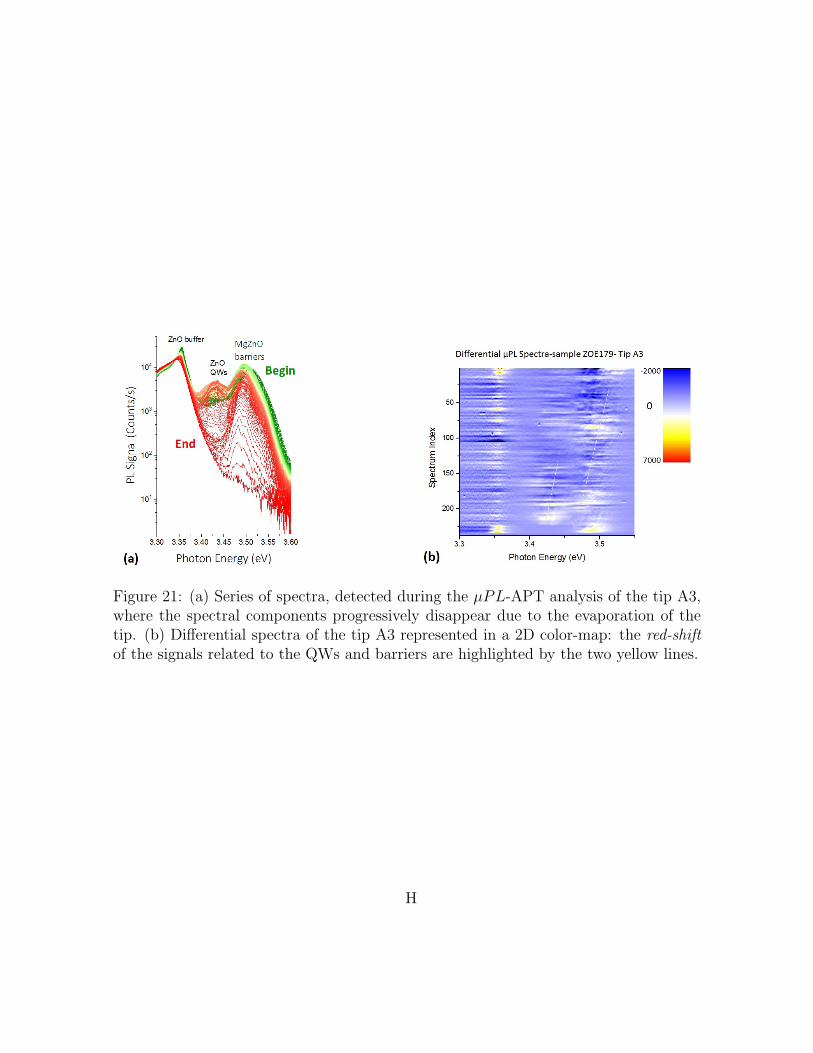
Figure 21: (a) Series of spectra, detected during the µPL-APT analysis of the tip A3,where the spectral components progressively disappear due to the evaporation of thetip. (b) Differential spectra of the tip A3 represented in a 2D color-map: the red-shiftof the signals related to the QWs and barriers are highlighted by the two yellow lines.
H

Aknowledgements
This thesis is the result of an important experience in my life. As any important expe-
rience, it was not carried out alone, but with a good company. For this reson, I would
like to express, in this last pages, my gratitude to the people who lived with me these
three years and gave me the motivation to arrive until the end, enjoying everyday.
My advisors: Angela Vella and Lorenzo Rigutti helped me to improve my scientific
skills, they were available to dialogue and to compare our point of views, always in a
good atmosphere. They helped me in order to highlight my natural aptidudes and so,
in this sense, they didn’t only represent my teachers for these three years, but they also
suggested me a possible direction to follow after this thesis.
My family: my mother Graziella, my father Claudio, my brother Federico and my rela-
tives, also if further, they were constantly present in order to sustain each other. They
were a continuous proof of faith and they showed me how it is possible to listen carefully
and to understand someone althought the distance.
My friends, in order to cite some of them: Mohamed, Souhaila, Federica, Mario, Ka-
mal, Elodie, Chantal, Kevi, Marie-Laure, Olha, Liz, Camille, Serena, Ludovica, Chiara,
Davide, Amalia, Sahar, Diana, Roger, Danut, all the people of the laboratory and of
course all the people with who it was really easy to share some time and be part of the
same team. To all these friends I am sincerely thankful, because they recharged my
energy, they sustained me and they helped me to find the positive attitude in order to
appreciate everyday.