Silicon nanowires prepared by thermal evaporation and their photoluminescence properties measured at...
6
Silicon nanowires prepared by thermal evaporation and their photoluminescence properties measured at low temperatures This content has been downloaded from IOPscience. Please scroll down to see the full text. Download details: IP Address: 219.92.238.25 This content was downloaded on 29/09/2013 at 00:38 Please note that terms and conditions apply. 2011 Adv. Nat. Sci: Nanosci. Nanotechnol. 2 015016 (http://iopscience.iop.org/2043-6262/2/1/015016) View the table of contents for this issue, or go to the journal homepage for more Home Search Collections Journals About Contact us My IOPscience
-
Upload
independent -
Category
Documents
-
view
5 -
download
0
Transcript of Silicon nanowires prepared by thermal evaporation and their photoluminescence properties measured at...

Silicon nanowires prepared by thermal evaporation and their photoluminescence properties
measured at low temperatures
This content has been downloaded from IOPscience. Please scroll down to see the full text.
Download details:
IP Address: 219.92.238.25
This content was downloaded on 29/09/2013 at 00:38
Please note that terms and conditions apply.
2011 Adv. Nat. Sci: Nanosci. Nanotechnol. 2 015016
(http://iopscience.iop.org/2043-6262/2/1/015016)
View the table of contents for this issue, or go to the journal homepage for more
Home Search Collections Journals About Contact us My IOPscience
IOP PUBLISHING ADVANCES IN NATURAL SCIENCES: NANOSCIENCE AND NANOTECHNOLOGY
Adv. Nat. Sci.: Nanosci. Nanotechnol. 2 (2011) 015016 (5pp) doi:10.1088/2043-6262/2/1/015016
Silicon nanowires prepared by thermalevaporation and their photoluminescenceproperties measured at low temperaturesVan Tuan Pham1, Van Ngoc Le2, Anh Tuan Chu3, Toan Thang Pham4,Ngoc Khiem Tran1, Hong Duong Pham3 and Thanh Huy Pham4
1 International Training Institute for Materials Science, Hanoi University of Technology, 1 Dai Co VietRoad, Hanoi, Vietnam2 Institute of Engineering Physics, Hanoi University of Technology, 1 Dai Co Viet Road, Hanoi, Vietnam3 Institute of Materials Science (IMS), Vietnam Academy of Science and Technology,18 Hoang Quoc Viet Road, Hanoi, Vietnam4 Hanoi Advanced School of Science and Technology, Hanoi University of Technology,1 Dai Co Viet Road, Hanoi, Vietnam
E-mail: [email protected]
Received 8 November 2010Accepted for publication 9 February 2011Published 14 March 2011Online at stacks.iop.org/ANSN/2/015016
AbstractIn the present work, silicon nanowires were prepared by a thermal evaporation method. Theevaporating source was a mixture of silicon and carbon nanopowders. Surface morphology,structural characteristics and emission properties of the silicon nanowires were investigated byseveral techniques. The results showed that the obtained products have the shape of nanowireswith diameters ranging from 30 to 120 nm and lengths from 300 to 400 nm. The x-raydiffraction (XRD) patterns confirmed the presence of crystalline silicon. Transmissionelectron microscope (TEM) images revealed the core-shell structure of the wires. In thephotoluminescence (PL) spectra recorded at room temperature, only a broad emission bandpeaking at about 650 nm was observed. In addition to the red emission, two other bandscentered at around 455 nm and 510 nm appeared when measured at low temperatures. Theorigin and emission mechanism of these bands are discussed.
Keywords: silicon nanowires, core-shell structure, thermal evaporation, photoluminescence
Classification numbers: 4.08, 5.03
1. Introduction
Silicon nanowires (Si NWs) have attracted much attentionin recent years because they exhibit different properties incomparison to their bulk counterparts [1–4]. The Si NWshave been synthesized by using different methods, such asCVD [5], laser ablation [1] and thermal evaporation [6].Among these methods, thermal evaporation shows manyadvantages, especially its low cost, ease of manufactureand relatively large yield. Various materials are used as anevaporating source to grow Si NWs, namely Si powder [7],SiO powder [6, 8], or a mixture of silicon and otherpowders, such as Fe powder [9], SiO2 powder [10], sulfurpowder [11] and zinc sulfide powder [12]. Also, different
growth mechanisms have been proposed for the formationof silicon nanowires, including vapor–liquid–solid (VLS),oxide-assisted growth (OAG) and sulfide-assisted growth.
Although crystalline silicon is the most used materialin the electronics industry, bulk silicon crystal is known tobe an indirect band-gap semiconductor and, consequently,it is a poor emitter of light even at low temperatures [13].Since the discovery of porous silicon with visible emissionat room temperature [14], the light-emitting properties of Sinanostructures in general, and of nanowires in particular, haveattracted considerable attention and have been investigatedwidely [15–24]. However, the PL properties of Si NWsmeasured at different temperatures have not been fullyexplored.
2043-6262/11/015016+05$33.00 1 © 2011 Vietnam Academy of Science & Technology
Adv. Nat. Sci.: Nanosci. Nanotechnol. 2 (2011) 015016 V T Pham et al
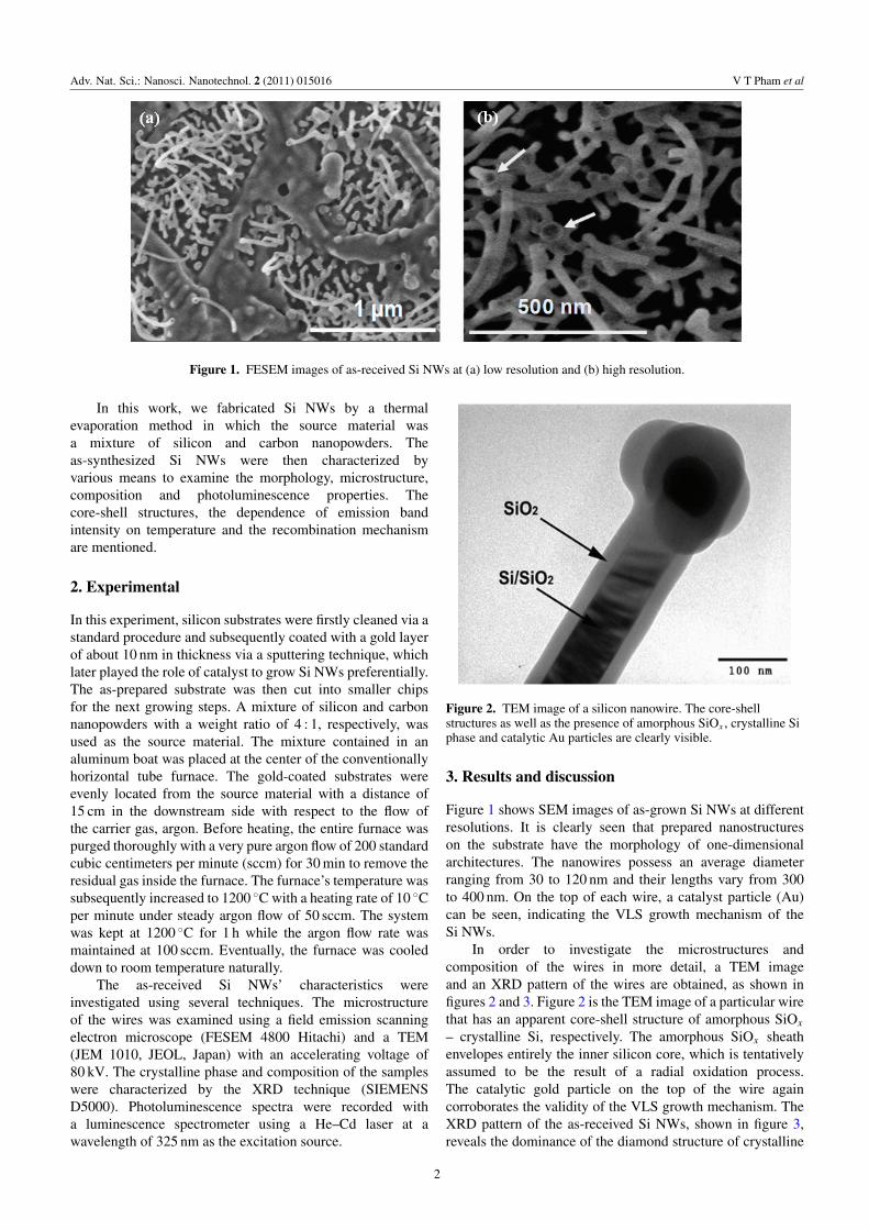
Figure 1. FESEM images of as-received Si NWs at (a) low resolution and (b) high resolution.
In this work, we fabricated Si NWs by a thermalevaporation method in which the source material wasa mixture of silicon and carbon nanopowders. Theas-synthesized Si NWs were then characterized byvarious means to examine the morphology, microstructure,composition and photoluminescence properties. Thecore-shell structures, the dependence of emission bandintensity on temperature and the recombination mechanismare mentioned.
2. Experimental
In this experiment, silicon substrates were firstly cleaned via astandard procedure and subsequently coated with a gold layerof about 10 nm in thickness via a sputtering technique, whichlater played the role of catalyst to grow Si NWs preferentially.The as-prepared substrate was then cut into smaller chipsfor the next growing steps. A mixture of silicon and carbonnanopowders with a weight ratio of 4 : 1, respectively, wasused as the source material. The mixture contained in analuminum boat was placed at the center of the conventionallyhorizontal tube furnace. The gold-coated substrates wereevenly located from the source material with a distance of15 cm in the downstream side with respect to the flow ofthe carrier gas, argon. Before heating, the entire furnace waspurged thoroughly with a very pure argon flow of 200 standardcubic centimeters per minute (sccm) for 30 min to remove theresidual gas inside the furnace. The furnace’s temperature wassubsequently increased to 1200 ◦C with a heating rate of 10 ◦Cper minute under steady argon flow of 50 sccm. The systemwas kept at 1200 ◦C for 1 h while the argon flow rate wasmaintained at 100 sccm. Eventually, the furnace was cooleddown to room temperature naturally.
The as-received Si NWs’ characteristics wereinvestigated using several techniques. The microstructureof the wires was examined using a field emission scanningelectron microscope (FESEM 4800 Hitachi) and a TEM(JEM 1010, JEOL, Japan) with an accelerating voltage of80 kV. The crystalline phase and composition of the sampleswere characterized by the XRD technique (SIEMENSD5000). Photoluminescence spectra were recorded witha luminescence spectrometer using a He–Cd laser at awavelength of 325 nm as the excitation source.
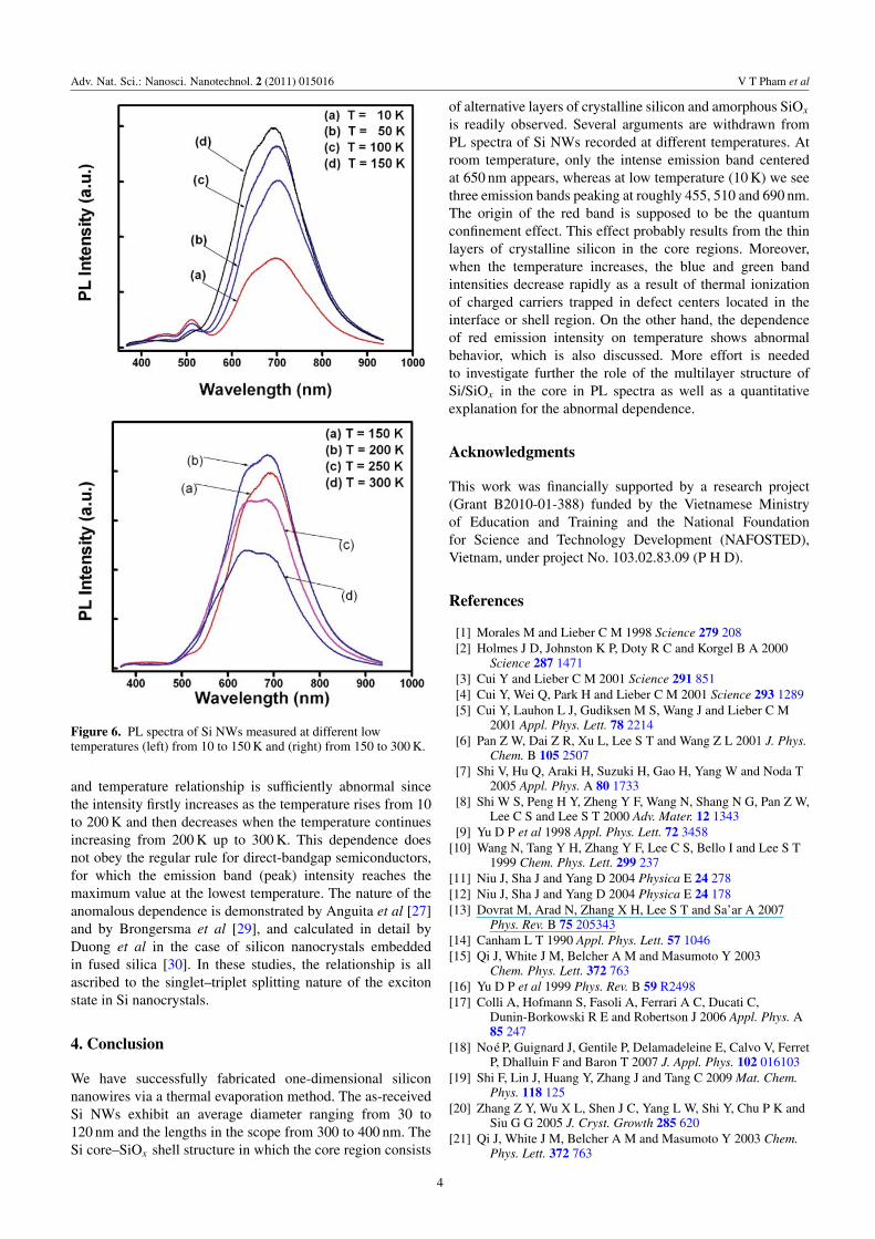
Figure 2. TEM image of a silicon nanowire. The core-shellstructures as well as the presence of amorphous SiOx , crystalline Siphase and catalytic Au particles are clearly visible.
3. Results and discussion
Figure 1 shows SEM images of as-grown Si NWs at differentresolutions. It is clearly seen that prepared nanostructureson the substrate have the morphology of one-dimensionalarchitectures. The nanowires possess an average diameterranging from 30 to 120 nm and their lengths vary from 300to 400 nm. On the top of each wire, a catalyst particle (Au)can be seen, indicating the VLS growth mechanism of theSi NWs.
In order to investigate the microstructures andcomposition of the wires in more detail, a TEM imageand an XRD pattern of the wires are obtained, as shown infigures 2 and 3. Figure 2 is the TEM image of a particular wirethat has an apparent core-shell structure of amorphous SiOx
– crystalline Si, respectively. The amorphous SiOx sheathenvelopes entirely the inner silicon core, which is tentativelyassumed to be the result of a radial oxidation process.The catalytic gold particle on the top of the wire againcorroborates the validity of the VLS growth mechanism. TheXRD pattern of the as-received Si NWs, shown in figure 3,reveals the dominance of the diamond structure of crystalline
2

Adv. Nat. Sci.: Nanosci. Nanotechnol. 2 (2011) 015016 V T Pham et al
Figure 3. XRD pattern of as-grown Si NWs. Characteristic peaksattributed to diamond Si and Au phases are marked.
silicon in the sample. Besides the strong peak assigned tothe Si phase, a relatively weak peak corresponding to the Auphase confirms the presence of gold particles.
The PL spectra of the wires recorded at room temperature(300 K) and 10 K are presented in figures 4(a) and (b),respectively. At room temperature, a broad emission bandcentered on 650 nm solely predominates. Similar results arereported by several authors [13, 25–27]. It is generallyaccepted that the origin of this red emission band in siliconnanostructures is attributed to the quantum confinement effect.However, as mentioned earlier, the average diameter ofas-grown Si NWs ranges from 30 to 80 nm, which is muchlarger than the Bohr radius characterized for silicon (5 nm).Fortunately, when observing carefully the TEM image ofthe wires in figure 2, we certainly discover the alternativepresence of dark and bright layers, which denotes the SiOx
and Si phases, respectively. Consequently, we propose thatthe core itself is an assembly of SiOx and Si regions wherethe dimensions of the Si regions are in the scale of its Bohrradius (5 nm). Furthermore, as examined at low temperature,10 K, we observe two more emission bands peaking roughlyat 455 nm and 510 nm in addition to the red emission bandnow shifted to ∼690 nm. In the literature, the blue emissionband centered at around 455 nm and the 525 nm green bandare attributed to the defects surrounding the silicon nanowire’scrystalline core [15]. Very recently, a short-lived visible bandin the photoluminescence spectrum of silicon nanocrystalsthat increases in intensity and shifts to longer wavelengthsfor smaller nanocrystals sizes was observed and assigned tothe radiative recombination of non-equilibrium electron–holepairs in a process that does not involve phonons [28].
The dependence of PL intensities of green and blue bandson temperature is shown in figure 5. We understandably seethat the PL intensities of these two bands decrease when thetemperature increases from 10 to 100 K. The result is in goodagreement with that reported by Qi et al [15] in which thermalquenching is supposed to stem from the thermal ionizationof charged carriers in defect centers either in the SiOx /Siinterface or in the SiOx sheath [15].
Figure 4. PL spectra of as-synthesized Si NWs measured at(a) 300 K and (b) 10 K.
Figure 5. PL spectra of the Si NWs measured at differenttemperatures from 10 to 100 K and focused in the wavelength rangeof 360–540 nm.
Finally, we investigated the effect of the temperature onthe intensities of the red emission band. The data are sketchedin figure 6. It is apparently seen that the emission intensity
3
Adv. Nat. Sci.: Nanosci. Nanotechnol. 2 (2011) 015016 V T Pham et al
Figure 6. PL spectra of Si NWs measured at different lowtemperatures (left) from 10 to 150 K and (right) from 150 to 300 K.
and temperature relationship is sufficiently abnormal sincethe intensity firstly increases as the temperature rises from 10to 200 K and then decreases when the temperature continuesincreasing from 200 K up to 300 K. This dependence doesnot obey the regular rule for direct-bandgap semiconductors,for which the emission band (peak) intensity reaches themaximum value at the lowest temperature. The nature of theanomalous dependence is demonstrated by Anguita et al [27]and by Brongersma et al [29], and calculated in detail byDuong et al in the case of silicon nanocrystals embeddedin fused silica [30]. In these studies, the relationship is allascribed to the singlet–triplet splitting nature of the excitonstate in Si nanocrystals.
4. Conclusion
We have successfully fabricated one-dimensional siliconnanowires via a thermal evaporation method. The as-receivedSi NWs exhibit an average diameter ranging from 30 to120 nm and the lengths in the scope from 300 to 400 nm. TheSi core–SiOx shell structure in which the core region consists
of alternative layers of crystalline silicon and amorphous SiOx
is readily observed. Several arguments are withdrawn fromPL spectra of Si NWs recorded at different temperatures. Atroom temperature, only the intense emission band centeredat 650 nm appears, whereas at low temperature (10 K) we seethree emission bands peaking at roughly 455, 510 and 690 nm.The origin of the red band is supposed to be the quantumconfinement effect. This effect probably results from the thinlayers of crystalline silicon in the core regions. Moreover,when the temperature increases, the blue and green bandintensities decrease rapidly as a result of thermal ionizationof charged carriers trapped in defect centers located in theinterface or shell region. On the other hand, the dependenceof red emission intensity on temperature shows abnormalbehavior, which is also discussed. More effort is neededto investigate further the role of the multilayer structure ofSi/SiOx in the core in PL spectra as well as a quantitativeexplanation for the abnormal dependence.
Acknowledgments
This work was financially supported by a research project(Grant B2010-01-388) funded by the Vietnamese Ministryof Education and Training and the National Foundationfor Science and Technology Development (NAFOSTED),Vietnam, under project No. 103.02.83.09 (P H D).
References
[1] Morales M and Lieber C M 1998 Science 279 208[2] Holmes J D, Johnston K P, Doty R C and Korgel B A 2000
Science 287 1471[3] Cui Y and Lieber C M 2001 Science 291 851[4] Cui Y, Wei Q, Park H and Lieber C M 2001 Science 293 1289[5] Cui Y, Lauhon L J, Gudiksen M S, Wang J and Lieber C M
2001 Appl. Phys. Lett. 78 2214[6] Pan Z W, Dai Z R, Xu L, Lee S T and Wang Z L 2001 J. Phys.
Chem. B 105 2507[7] Shi V, Hu Q, Araki H, Suzuki H, Gao H, Yang W and Noda T
2005 Appl. Phys. A 80 1733[8] Shi W S, Peng H Y, Zheng Y F, Wang N, Shang N G, Pan Z W,
Lee C S and Lee S T 2000 Adv. Mater. 12 1343[9] Yu D P et al 1998 Appl. Phys. Lett. 72 3458
[10] Wang N, Tang Y H, Zhang Y F, Lee C S, Bello I and Lee S T1999 Chem. Phys. Lett. 299 237
[11] Niu J, Sha J and Yang D 2004 Physica E 24 278[12] Niu J, Sha J and Yang D 2004 Physica E 24 178[13] Dovrat M, Arad N, Zhang X H, Lee S T and Sa’ar A 2007
Phys. Rev. B 75 205343[14] Canham L T 1990 Appl. Phys. Lett. 57 1046[15] Qi J, White J M, Belcher A M and Masumoto Y 2003
Chem. Phys. Lett. 372 763[16] Yu D P et al 1999 Phys. Rev. B 59 R2498[17] Colli A, Hofmann S, Fasoli A, Ferrari A C, Ducati C,
Dunin-Borkowski R E and Robertson J 2006 Appl. Phys. A85 247
[18] Noé P, Guignard J, Gentile P, Delamadeleine E, Calvo V, FerretP, Dhalluin F and Baron T 2007 J. Appl. Phys. 102 016103
[19] Shi F, Lin J, Huang Y, Zhang J and Tang C 2009 Mat. Chem.Phys. 118 125
[20] Zhang Z Y, Wu X L, Shen J C, Yang L W, Shi Y, Chu P K andSiu G G 2005 J. Cryst. Growth 285 620
[21] Qi J, White J M, Belcher A M and Masumoto Y 2003 Chem.Phys. Lett. 372 763
4

Adv. Nat. Sci.: Nanosci. Nanotechnol. 2 (2011) 015016 V T Pham et al
[22] Tong D H, Tran P D, Pham X T T, Pham V B, Le T T T, DangM C and Van Rijn C J M 2010 Adv. Nat. Sci.: Nanosci.Nanotechnol. 1 015011
[23] Xuan T T P, Le T T T, Tran P D, Pham B V, Tong D H andDang M C 2010 Adv. Nat. Sci.: Nanosci. Nanotechnol.1 025013
[24] Le T T T, Tran P D, Pham X T, Tong D H and Dang M C 2010Adv. Nat. Sci.: Nanosci. Nanotechnol. 1 035004
[25] Zeng X B, Liao X B, Wang B, Dai S T, Xu Y Y, Xiang X B,Hua Z H, Diao H W and Kong G L 2004 J. Cryst. Growth265 94
[26] Shi F, Lin J, Huang Y, Zhang J and Tang C 2009 Mat. Chem.Phys. 118 125
[27] Anguita J V, Sharma P, Henley S J and Silva S R P 2009 IOPConf. Series: Mater. Sci. Eng. 6 012011
[28] De Boer W D A M, Timmerman S, Dohnalová K, Yassievich IN, Zhang H, Buma W J and Gregorkiewicz T 2010 Nat.Nanotechnol. 5 878
[29] Brongersma M L, Kik P G, Polman A, Min K S and Atwater HA 2000 Appl. Phys. Lett. 76 351
[30] Duong P H, Lavallard P, Oliver A and Itoh T 2003 Phys. Stat.Sol. c 0 1271
5