From carbon nanostructures to new photoluminescence ...
13
DOI: 10.1002/cvde.200604034 Review From Carbon Nanostructures to New Photoluminescence Sources: An Overview of New Perspectives and Emerging Applications of Low-Pressure PECVD** By Francisco J. Gordillo-Vázquez,* Víctor J. Herrero , and Isabel Tanarro Low-pressure, plasma-enhanced (PE)CVD is a powerful and versatile technique that has been used for thin-film deposition and surface treatment since the early 1960s. However, it is only recently that it has been used in applications other than the different stages of microelectronic circuit fabrication. Now, PECVD is being used in emerging applications due to new mate- rials and process requirements in a wide variety of areas, such as biomedical applications, solar cells, fuel cell development, fusion research, or the synthesis of silicon nanocrystals showing efficient photoluminescence, useful for future solid-state light sources. These new scenarios have stimulated further development of novel PECVD diagnostic techniques, together with fun- damental experimental and theoretical studies aimed at a better understanding of some of the basic processes underlying the plasma/surface interaction. This paper gives an overview of some new research areas where PECVD is finding promising ap- plications. Keywords:Biomedical applications, Nanoparticles, Novel diagnostics, PECVD, Plasma 1. Introduction The early papers by S. W. Ing [1–3] and co-workers, pub- lished between 1963 and 1965 on low-temperature, plasma- enhanced CVD (or simply PECVD) deposition of silicon oxide films, could be considered as one of the first experi- mental reports on the possibility of using electric dis- charges in gases to produce plasmas that generate various types of reactive species for thin film deposition. These ini- tial attempts were used for microelectronic applications and, in particular, for diffusion masks and passivation. In this regard, the introduction in 1974 of commercial batch processing reactors was a definite step for serious consideration of plasma-assisted deposition processes in microelectronic circuit production lines. [4] With time, low- pressure plasma deposition of inorganic films, such as sili- con-based semiconductors and insulators, has been gradu- ally moving out of the integrated circuit (IC) industry to new applications in solar cells, [5] thin-film transistors, [6,7] flat-panel displays, or micro-electromechanical systems (MEMS). [8] More recently, the superior optical properties of nanocrystalline silicon (nc-Si:H) in comparison with those of hydrogenated amorphous silicon (a-Si:H) have stimulated research on nanostructured silicon films for photovoltaic applications. [9–13] The interest in silicon nano- particles extends to the production of single-electron tran- sistors, [14] new memory devices, [15] quantum dot lasers, [16] and especially new solid-state light sources based on the efficient room temperature photoluminescence of silicon nanocrystals [17–21] produced by low-pressure PECVD. Apart from the plasma synthesis of inorganic films, the first two reports on the synthesis of carbonaceous films by plasma-assisted CVD date back to 1976. These two papers employed low-pressure DC [22] and RF (13.56 MHz) [23] dis- Chem. Vap. Deposition 2007, 13, 267–279 © 2007 WILEY-VCH Verlag GmbH & Co. KGaA, Weinheim 267 – [*] Dr. F. J. Gordillo-Vázquez Instituto de Óptica, CSIC Serrano 121, 28006 Madrid (Spain) E-mail: [email protected] Dr.V. J. Herrero, Dr. I. Tanarro Instituto de Estructura de la Materia, CSIC Serrano 123, 28006 Madrid (Spain) [**] FJGV acknowledges partial financial support from CSIC-CAM (Pro- ject No. 200550M016 and 200650M016) and MEC (Projects No. MAT2006-13006-C02-01 and ENE2006-14577-C04-03), VJH and IT acknowledge funding from MEC (Projects No. FTN-2003-08228-C03- 03, FIS2004-00456 and ENE2006-14577-C04-03)
-
Upload
khangminh22 -
Category
Documents
-
view
0 -
download
0
Transcript of From carbon nanostructures to new photoluminescence ...

DOI: 10.1002/cvde.200604034
Review
From Carbon Nanostructures to NewPhotoluminescence Sources: An Overviewof New Perspectives and EmergingApplications of Low-Pressure PECVD**
By Francisco J. Gordillo-Vázquez,* Víctor J. Herrero,and Isabel Tanarro
Low-pressure, plasma-enhanced (PE)CVD is a powerful and versatile technique that has been used for thin-film depositionand surface treatment since the early 1960s. However, it is only recently that it has been used in applications other than thedifferent stages of microelectronic circuit fabrication. Now, PECVD is being used in emerging applications due to new mate-rials and process requirements in a wide variety of areas, such as biomedical applications, solar cells, fuel cell development,fusion research, or the synthesis of silicon nanocrystals showing efficient photoluminescence, useful for future solid-state lightsources. These new scenarios have stimulated further development of novel PECVD diagnostic techniques, together with fun-damental experimental and theoretical studies aimed at a better understanding of some of the basic processes underlying theplasma/surface interaction. This paper gives an overview of some new research areas where PECVD is finding promising ap-plications.
Keywords: Biomedical applications, Nanoparticles, Novel diagnostics, PECVD, Plasma
1. Introduction
The early papers by S. W. Ing[1–3] and co-workers, pub-lished between 1963 and 1965 on low-temperature, plasma-enhanced CVD (or simply PECVD) deposition of siliconoxide films, could be considered as one of the first experi-mental reports on the possibility of using electric dis-charges in gases to produce plasmas that generate varioustypes of reactive species for thin film deposition. These ini-tial attempts were used for microelectronic applicationsand, in particular, for diffusion masks and passivation.
In this regard, the introduction in 1974 of commercialbatch processing reactors was a definite step for seriousconsideration of plasma-assisted deposition processes inmicroelectronic circuit production lines.[4] With time, low-pressure plasma deposition of inorganic films, such as sili-con-based semiconductors and insulators, has been gradu-ally moving out of the integrated circuit (IC) industry tonew applications in solar cells,[5] thin-film transistors,[6,7]
flat-panel displays, or micro-electromechanical systems(MEMS).[8] More recently, the superior optical propertiesof nanocrystalline silicon (nc-Si:H) in comparison withthose of hydrogenated amorphous silicon (a-Si:H) havestimulated research on nanostructured silicon films forphotovoltaic applications.[9–13] The interest in silicon nano-particles extends to the production of single-electron tran-sistors,[14] new memory devices,[15] quantum dot lasers,[16]
and especially new solid-state light sources based on theefficient room temperature photoluminescence of siliconnanocrystals[17–21] produced by low-pressure PECVD.
Apart from the plasma synthesis of inorganic films, thefirst two reports on the synthesis of carbonaceous films byplasma-assisted CVD date back to 1976. These two papersemployed low-pressure DC[22] and RF (13.56 MHz)[23] dis-
Chem. Vap. Deposition 2007, 13, 267–279 © 2007 WILEY-VCH Verlag GmbH & Co. KGaA, Weinheim 267
–
[*] Dr. F. J. Gordillo-VázquezInstituto de Óptica, CSICSerrano 121, 28006 Madrid (Spain)E-mail: [email protected]
Dr. V. J. Herrero, Dr. I. TanarroInstituto de Estructura de la Materia, CSICSerrano 123, 28006 Madrid (Spain)
[**] FJGV acknowledges partial financial support from CSIC-CAM (Pro-ject No. 200550M016 and 200650M016) and MEC (Projects No.MAT2006-13006-C02-01 and ENE2006-14577-C04-03), VJH and ITacknowledge funding from MEC (Projects No. FTN-2003-08228-C03-03, FIS2004-00456 and ENE2006-14577-C04-03)

charges to decompose mixtures of ethylene/argon andmethane/argon, respectively. In 1985, the work by Matsu-moto et al.[24] showed the first evidence of the synthesis ofpolycrystalline diamond films from low-pressure MW(2.45 GHz) methane/molecular hydrogen plasmas. Furtherinvestigations starting in the late 1980s up to now haveshown the feasibility of using RF and MW-driven, low-pres-sure PECVD to produce different kinds of carbon-basednanostructures (nano[25—27] or ultrananoparticles,[28] nano-tubes,[29] nanowalls,[30] or nanotips[30]) from a mixture of ahydrocarbon gas (or H-free precursors like C60) and otherfunctional gases (H2, N2, NH3, Ar, He...).
Systematic investigation of plasma polymerizationstarted only in the 1960s after the pioneering work pub-lished by J. Goodman in 1960[31] showing the relevant di-electric properties of one micrometer thick film of poly-merized styrene deposited by plasma. Soon after this, in1969, the work by Hollahan et al.[32] experimentally provedthe possibility of using low-pressure ammonia plasmas toproduce amino groups able to attach to the surfaces of var-ious polymers with the goal of producing new materialscompatible with human blood. Since then, intensive re-search has been carried out by using low-pressure PECVDfor a variety of biomedical applications.
In the following sections of this review, we will coversome of the many emerging fields where low-pressurePECVD is having a renewed and key interest in surfacetreatment and film deposition (see Fig. 1) together with thedescription of novel diagnostic tools for PECVD and re-cent advances in fundamental research. This review beginswith basic issues and then moves on to specific applica-tions.
2. Surface Processes in Reactive Plasmas
The interaction between the plasma and the depositionsubstrate in PECVD involves, in general, a large amount ofconcurrent intertwined processes,[33–36] whose combined ef-fects are difficult to unravel. The interplay between deposi-tion and erosion ultimately responsible for film growth,
and the actual morphology and properties of the formedfilms, are often determined by synergies between several ofthe participating species which are, in turn, dependent onthe physical characteristics of the plasma and of the sub-strate. Despite many efforts by various groups, the basicmechanisms are often poorly understood and the optimiza-tion of film growth for technical applications is usuallydealt with empirically. However, over the last few years, de-tailed studies using a variety of experimental techniques,involving notably molecular beams and lasers, are begin-ning to shed some light on the key species and processesinvolved in plasma/surface interactions for some relevantcases. We will comment here briefly on some of these re-cent achievements.
The main reactive species interacting with the surfaceare ions and radicals (including atoms). Although radicalsare usually the dominant growth precursors in the low-tem-perature, weakly ionized plasmas employed for PECVD,ions can also influence the deposition process in several im-portant ways; they can contribute to film growth either bydirect implantation or by creating reactive sites on the sur-face, and they can also erode the film by physical sputtering(see Fig. 2). The most abundant radicals in the gas phasedo not necessarily play an important role in PECVD. Ac-tual growth precursors will typically have high stickingcoefficients and much lower gas phase concentrations. Thesearch for growth precursors in deposition plasmas thus re-quires the use of sensitive detection techniques for radicals.
F. J. Gordillo-Vázquez et al./New Applications for Low-Pressure PECVD
268 www.cvd-journal.de © 2007 WILEY-VCH Verlag GmbH & Co. KGaA, Weinheim Chem. Vap. Deposition 2007, 13, 267–279
Francisco José Gordillo Vázquez is a tenured scientist at the Spanish Nacional ResearchCouncil (CSIC) in Madrid. Since 1998, his research activity has been focused on low-pressureplasma-enhanced Chemical Vapor Deposition (PECVD) of carbon films and coatings, in par-ticular the diagnosis and kinetic modeling of hydrocarbon-argon/hydrogen plasmas of interestfor the synthesis of amorphous carbon, diamond and doped/undoped nanodiamond thinfilms. In 2001, he started to research plasmas formed during the process of pulsed laser deposi-tion (PLD) of dielectric material coatings for optical applications. He is also the organizer ofthe 19th European Conference on the Atomic and Molecular Physics of Ionized Gases to beheld in Granada, Spain in July 2008. Some of his recent projects include the kinetic modelingof acetylene/argon plasmas with and without molecular nitrogen of interest in the synthesis ofcarbon nanostructured films, and experimental and theoretical analysis of the role played bypolycyclic aromatic hydrocarbons in the synthesis of carbonaceous interstellar dust analogparticles within laboratory low-pressure hydrocarbon plasmas.
Low pressure non-thermal plasmas in PECVD
Te >> Tg ≅ 400 K -1000 K
Very reactive species
Non-equilibrium chemistry
Surface Treatment Thin Film Deposition
Fig. 1. Main features of the plasmas produced in low-pressure PECVD andapplications.

An overview of plasma diagnostics techniques is given inthe next section. Whenever possible, a simultaneous moni-toring of gas phase composition and film growth is desir-able.
In recent times, the basic physicochemical mechanismsresponsible for the deposition of amorphous hydrogenatedcarbon (a-C:H) films in methane plasmas have been inves-tigated thoroughly by Jacob, von Keudell, and co-workersin a series of works combining various experimental tech-niques.[35,37–45] In addition to the primary radicals formed inthe dissociation of the precursor (CH3, CH2, CH, C), sec-ondary reaction products generated in the course of plasmareactions can be also directly incorporated into the growingfilm. In this respect, the important role of unsaturated hy-drocarbon radicals, in particular C2H and C2H3, with highsticking coefficients should be stressed. Refined particlebeam experiments[43] have shown that H atoms and ionscan largely enhance the adsorption probability of a givenradical through the production of chemisorption sites, espe-cially dangling bonds, on an otherwise hydrogen-termi-nated surface. This effect is especially marked in the caseof CH3, whose sticking coefficient can increase from 10–4 to10–2. In spite of this enhancement, the sticking coefficientremains low, and consequently methyl radicals reach rela-tively large concentrations in the gas phase, but do notusually play an important role in film growth. Finally, low-energy carbonaceous ions impinging on the growing filmalso have high sticking probabilities and can contribute tofilm growth. These ions do not produce appreciable sput-tering effects for energies below ≈500 eV. The prevalenceof a given growth precursor or mechanism has been foundto be closely related to the mean energy dissipated by
source gas molecule in the plasma, Emean.[45] For Emean
< 10 eV, film growth is mainly caused by incorporation ofCH radicals (see Fig. 3). For intermediate energies, higherhydrocarbon radicals (C2H, C2H3) are the dominantgrowth precursors, and only for values of Emean > 100 eV,carbonaceous ions begin to contribute appreciably to filmgrowth.
Plasma/surface interactions have also deserved much at-tention in fluorocarbon (FC) plasmas, which find wide-spread application in the etching of Si and SiO2 and in thedeposition of fluorocarbon films. In general there is a deli-cate balance between deposition and etching that dependssensitively on the precursor and on the type of dischargeused. In early works, it was suggested that CF2 might be themain precursor for film growth,[46,47] however it was latershown that under polymerizing conditions the radical has along lifetime and reaches a high concentration, indicative ofa low sticking probability. Experiments using space- andtime-resolved, laser-induced fluorescence (LIF) and abso-lute calibration techniques[48,49] have established that CFand CF2 radicals are produced essentially at the surfaces,and that the actual film precursors are oligomers of theCxFy(CF2)n type formed in gas-phase polymerization reac-tions of the relatively abundant CF2 radicals. The produc-tion of CF2 at the surface of the forming FC films, and thelow sticking probability of the radical, were also observedby Fisher and co-workers,[50] who conducted detailed experi-ments on various plasma precursors using the “imaging ofradicals interacting with surfaces” (IRIS) technique,[51]
which combines molecular beams and LIF imaging methods.The enhancement in CF2 production through ion bombard-ment has also been investigated by this group.[50,52] Other as-pects of the behavior of CFx radicals in fluorocarbon plas-mas are presently being studied by various groups.[53,54]
The surface reactivity of other radicals has also beenstudied using the IRIS technique.[55] In particular, CH, SiH,
F. J. Gordillo-Vázquez et al./New Applications for Low-Pressure PECVD
Chem. Vap. Deposition 2007, 13, 267–279 © 2007 WILEY-VCH Verlag GmbH & Co. KGaA, Weinheim www.cvd-journal.de 269
Inelastic
collisions
c) Transport to surface
ENERGY from APPLIED FIELD
Excitation, Dissociation,
Ionization, …
Electron attachment
(negative
ions)
Low energy
electrons
SUBSTRATE
a) Initial reactions
d) Surface reactions
High energy
electrons
Power supply
b) Formation of excited speciesand nanoclusters
Free
radicals
Nanoclusters
Fig. 2. Sketch of the processes taking place during low-pressure PECVD.
C2H + C2H3
CH
ions
1 10 100
1014
1013
1012
sum
Emean (eV)
Γ (c
m–2
)
Fig. 3. Fluence of incorporated carbon atoms per cycle Ggrowth deposited ina methane ICP at 2 Pa (open circles) as a function of Emean compared withthe growth contribution per cycle of GCH (dashed line), C2H� C2H3
, and GC
in CnHm+ (dotted line). The solid line represents the sum of the three contri-
butions. (Reproduced with permission from [45]. Copyright 2005, AmericanInstitute of Physics).

and CN were found to be “sticky” with high surface reac-tivity, whereas NH and SiCl2 do not tend to stick to the sur-face of growing films. The authors of these studies indicatea possible correlation between surface reactivity and elec-tronic structure of the radicals; species with a doublet elec-tron configuration are found to have a high reactivitywhereas those with a singlet configuration tend to be gener-ated at the surface during film deposition. These findingswarrant further experimental and theoretical work in orderto corroborate this correlation and to provide insight intothe underlying mechanisms.
Growth mechanisms have also been investigated in re-cent times for the deposition of films of SiCxNy ternarycompounds.[56] In low-voltage RF discharges, SiH3 andC2H radicals are deemed to contribute independently tothe carbon nitride and silicon nitride networks. In high-voltage glow discharges, bonds between the three compo-nents are apparently formed by subplantation and damage-induced disorder, giving rise to harder films.
A sound understanding of the physical chemistry behindPECVD will require a theoretical description of, at least,the most relevant plasma surface interactions, which aremuch more complicated than their gas-phase counterparts.Progress in the theoretical treatment of the surface has ledto models incorporating different growth structures,[36] orthe effects of ion bombardment on the growing films.[57]
However, theoretical models are still relatively rudimen-tary and have no predictive power due to, in most cases, alack of proper verification and validation of computationalsimulations. Progress in this field is also severely hamperedby the lack of reliable kinetic data (either from experimentor theory) for many of the elementary processes involved.
3. Diagnostic Techniques
So far, the development of plasma processing has mostlybeen carried out by a trial and error method changing ex-ternal parameters (basically dependent on the reactor)such as power, pressure, and gas mixture ratios, whereasthe inside state of the plasma was unknown; nevertheless,the processes of interest can be characterized much moreproperly employing internal parameters such as ion andradical densities and their energies. To obtain a completeset of the main plasma properties, several complementaryexperimental techniques are available.
There exist a very high number and variety of plasma di-agnostic methods and only a brief overview will be givenhere. A scheme including some of them is given in Fig-ure 4. As entities that are intrinsically light-emittingsources, plasmas can be characterized first of all by emis-sion spectroscopy. This technique has been used for de-cades to identify the existing species with a high degree ofconfidence and sensitivity; nevertheless it can barely pro-vide estimations of species concentrations. In order to getreliable relative concentrations from emission data, recent
improvements in diagnostics and a more precise knowledgeof excitation cross-sections[58,59] have opened new possibili-ties and alternatives[60,61] to the formerly well-establishedmethod of actinometry.
Broadband light-emitting sources, such as cyclotron radi-ation and high resolution laser sources extending from theMW to the VUV region, have stimulated noticeably theuse of direct absorption spectroscopic techniques fromground and excited levels to study the electronic, vibra-tional, and rotational molecular transitions, providing di-rect and detailed information about absolute concentra-tions of the detected species and their characteristictemperatures, which may be far from equilibrium and differfor the various energy modes. High-power lasers, pulsed orcontinuous, have also allowed the development of othervery sensitive techniques such as LIF and resonance-en-hanced multiphoton ionization (REMPI). A valuable com-pilation of spectroscopic data and references for polya-tomic ions and neutral transients, including commentsabout the specific detection techniques, is given in the lit-erature.[62] An interesting description of the presently mostemployed spectrometric methods for the detection of radi-cals can also be found in the literature.[63] Among the pres-ently available experimental methods based on the use oflasers for plasma diagnostics, diode laser absorption andthe very sensitive technique of cavity ring-down spectrosco-py[64,65] have experienced great advances during the lastyears. The recently developed quantum cascade lasers op-erating with short IR pulses at room temperature are verypromising mid-infrared radiation sources for plasma char-acterization.[66,67] All of these spectroscopic methods havethe great advantage of being non-intrusive. Nevertheless,the geometry of the reactor should be frequently adaptedto the diagnostic technique to be used, and this is not al-ways the case in production reactors. For example, long op-tical path lengths (single or in multipass configuration) areneeded for absorption spectroscopy of transient specieswhich appear at very low densities in the plasma.
F. J. Gordillo-Vázquez et al./New Applications for Low-Pressure PECVD
270 www.cvd-journal.de © 2007 WILEY-VCH Verlag GmbH & Co. KGaA, Weinheim Chem. Vap. Deposition 2007, 13, 267–279
Laser Beam
MultipassCell
PowerSupply
LangmuirProbe
MassSpectrometer
Mono-chromator
CatalyticProbe
CCD
Vacuum Pumps
PLASMA
Substrate
Fig. 4. Simplified scheme of a PECVD reactor showing some of the variousplasma diagnostic techniques mentioned in the text.

Electron temperature, plasma density, and plasma poten-tial are measured with electric (Langmuir) probes insertedinto the plasma. In this case, special care should be paidto minimize the perturbations caused by the probes on theoriginal plasma conditions. Continuous improvements inthis method for various kinds of plasmas are being devel-oped. A recent and complete revision on the use of electri-cal probes can be found in the literature.[68]
Mass spectrometry of ions with analysis of the ion energydistribution functions,[69,70] ion attachment mass spectrome-try,[71] the use of different isotopes and mass spectrometryat threshold energies for radical detection,[72,73] are alsovery useful tools for plasma diagnostics, which have addednew possibilities to the conventional mass spectrometry ofneutral stable species with ionization by electron impact,where the detection of minor products has been mostlyhampered by overlapping signals with peaks proceedingfrom the fragmentation patterns of compounds present athigher concentrations.
Fiber-optic catalytic probes of various materials are be-ginning to be used to measure the dissociation degree ofpure gases such as H2, O2, or N2 in the afterglow of plasmareactors.[74] Dust particles formed in the plasmas, which aregetting increasing attention because of their influence onthe final quality of the treated surfaces, are now monitoredby light scattering.[75] In this way, a very characteristic peri-odic increase and decrease of dust density and average sizehas been found, even in non-modulated discharges, con-trolled by gravity. On the other hand, on/off plasma modu-lation, which controls in time the concentrations of short-lived species, allows the application of several of the formermentioned diagnostic techniques to time-resolved plasmastudies,[76] which add valuable information on reactioncoefficients and wall reaction probabilities[77] and opensnew insights in deposition processes with minimum dustproduction.[78]
Concerning plasma surface interactions, a recent simplemethod to determine surface loss probabilities employs adismountable cavity with a small entrance slit exposed tothe reactive species,[44] which allows a later study of thedeposited materials in the internal surfaces. Ion and neutralparticle-beam experiments allow a much more detailed de-termination of sticking coefficients.[43]
4. Nanofabrication and Quantum ConfinementStructures
Nanostructured materials are expected to bring aboutmajor advances in electronics and photonics in the courseof the next decades.[79] In nanometer-sized semiconductorsand metals, the de Broglie wavelength of the electrons andholes becomes comparable to the dimensions of the rele-vant crystallites, and the valence and conduction bandsmay split into discrete electronic levels whose spacing, aswell as that of the band-gap, increases with decreasing par-
ticle size.[80] Quantized matter can adopt different shapes(dots, wires, ...) depending on the quantization dimensions.Several procedures have been devised for the productionof nanoscaled materials, including colloid chemistry, self as-sembly, lithographic etching, and thin film deposition. Theuse of reactive plasmas as a versatile nanofabrication toolhas been recently reviewed by Ostrikov.[30]
In general, in nanofabrication processes adequate build-ing units must be generated, transported, and stacked ontosuitably prepared surfaces. PECVD often provides a goodopportunity for the generation of a large variety of buildingunits. Besides the molecules present in the feedstock gases,atoms, ions, and radicals are generated by electron impactor by subsequent chemical reactions. In addition, negativeions within the plasma are confined by the plasma sheathand can eventually reach relatively high concentrations,giving rise to polymerization and clustering through reac-tions with other plasma species. In contrast, the number ofbuilding units in thermal CVD, without ions or clusters, ismore limited and deposition rates are significantly slowerthan in PECVD. Another advantage of plasma-assisted de-position over CVD is the fact that ion bombardment canactivate surface sites for reaction without the need to heatthe substrate. With an adequate choice of the feedstockgases and type of discharge, one can favor the formation ofdeposition precursors suitable for each case. Given the lowpressures typical of most PECVD reactors, very few colli-sions take place in the plasma sheath and, once generated,the smaller building units travel undisturbed to the sub-strate; the larger building units (>1 nm) can be subject todrag or thermophoretic forces that can be used advanta-geously for the control of the deposition process.[81] In gen-eral, for good quality films, the building units should notdisintegrate or damage the surface upon landing.
The production of silicon- and carbon-based nanoassem-blies are the most thoroughly studied plasma-assisted nano-fabrication processes and, although the basic mechanismsresponsible for the formation of the various structures re-main largely unknown, general rules and practical recipesare available in the literature.[30] Reactive carbon dimers,C2, are known, for instance, to be efficient for the growthof carbon nanotubes (CNTs) because they can insert easilyinto the hexagonal units of the graphene sheets that buildthe CNT walls (see below). Charged carbon clusters in thenanometer scale can be very adequate for the synthesis ofsingle-crystalline diamond or of crystalline graphite.[30] Incontrast to CH3, whose sticking coefficient was seen to besmall in general,[44] the SiH3 radical, which has a pyramidalstructure, contributes efficiently to the growth ofa-Si:H.[35,82] Large silanes and hydrogenated Si clusters alsoplay a key role in the PECVD of nanostructured amor-phous silicon films for solar cell applications. In some cases,the size and concentration of clusters in the discharge hasbeen correlated with the microstructural parameters defin-ing the film quality.[83] Nanoparticles generated in theplasma can also be incorporated into the growing films.
F. J. Gordillo-Vázquez et al./New Applications for Low-Pressure PECVD
Chem. Vap. Deposition 2007, 13, 267–279 © 2007 WILEY-VCH Verlag GmbH & Co. KGaA, Weinheim www.cvd-journal.de 271
Polymorphous silicon (pm-Si:H), which is formed by anamorphous matrix with nanocrystalline inclusions and canlead to a significant improvement of the performance ofsolar cells, has been obtained with this procedure.[84,85] Arecent computational study suggests that the formation ofcrystalline hydrogenated Si nanoparticles could be favoredby the use of hotter silane plasmas.[86]
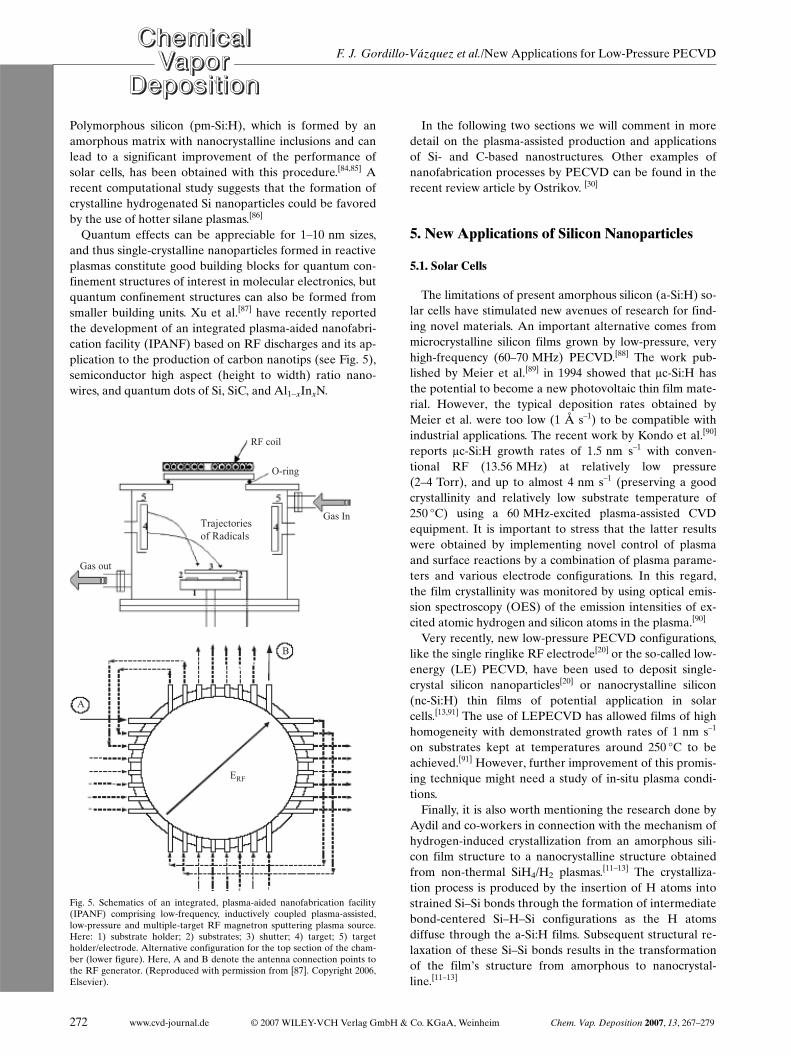
Quantum effects can be appreciable for 1–10 nm sizes,and thus single-crystalline nanoparticles formed in reactiveplasmas constitute good building blocks for quantum con-finement structures of interest in molecular electronics, butquantum confinement structures can also be formed fromsmaller building units. Xu et al.[87] have recently reportedthe development of an integrated plasma-aided nanofabri-cation facility (IPANF) based on RF discharges and its ap-plication to the production of carbon nanotips (see Fig. 5),semiconductor high aspect (height to width) ratio nano-wires, and quantum dots of Si, SiC, and Al1–xInxN.
In the following two sections we will comment in moredetail on the plasma-assisted production and applicationsof Si- and C-based nanostructures. Other examples ofnanofabrication processes by PECVD can be found in therecent review article by Ostrikov. [30]
5. New Applications of Silicon Nanoparticles
5.1. Solar Cells
The limitations of present amorphous silicon (a-Si:H) so-lar cells have stimulated new avenues of research for find-ing novel materials. An important alternative comes frommicrocrystalline silicon films grown by low-pressure, veryhigh-frequency (60–70 MHz) PECVD.[88] The work pub-lished by Meier et al.[89] in 1994 showed that lc-Si:H hasthe potential to become a new photovoltaic thin film mate-rial. However, the typical deposition rates obtained byMeier et al. were too low (1 Å s–1) to be compatible withindustrial applications. The recent work by Kondo et al.[90]
reports lc-Si:H growth rates of 1.5 nm s–1 with conven-tional RF (13.56 MHz) at relatively low pressure(2–4 Torr), and up to almost 4 nm s–1 (preserving a goodcrystallinity and relatively low substrate temperature of250 °C) using a 60 MHz-excited plasma-assisted CVDequipment. It is important to stress that the latter resultswere obtained by implementing novel control of plasmaand surface reactions by a combination of plasma parame-ters and various electrode configurations. In this regard,the film crystallinity was monitored by using optical emis-sion spectroscopy (OES) of the emission intensities of ex-cited atomic hydrogen and silicon atoms in the plasma.[90]
Very recently, new low-pressure PECVD configurations,like the single ringlike RF electrode[20] or the so-called low-energy (LE) PECVD, have been used to deposit single-crystal silicon nanoparticles[20] or nanocrystalline silicon(nc-Si:H) thin films of potential application in solarcells.[13,91] The use of LEPECVD has allowed films of highhomogeneity with demonstrated growth rates of 1 nm s–1
on substrates kept at temperatures around 250 °C to beachieved.[91] However, further improvement of this promis-ing technique might need a study of in-situ plasma condi-tions.
Finally, it is also worth mentioning the research done byAydil and co-workers in connection with the mechanism ofhydrogen-induced crystallization from an amorphous sili-con film structure to a nanocrystalline structure obtainedfrom non-thermal SiH4/H2 plasmas.[11–13] The crystalliza-tion process is produced by the insertion of H atoms intostrained Si–Si bonds through the formation of intermediatebond-centered Si–H–Si configurations as the H atomsdiffuse through the a-Si:H films. Subsequent structural re-laxation of these Si–Si bonds results in the transformationof the film’s structure from amorphous to nanocrystal-line.[11–13]
F. J. Gordillo-Vázquez et al./New Applications for Low-Pressure PECVD
272 www.cvd-journal.de © 2007 WILEY-VCH Verlag GmbH & Co. KGaA, Weinheim Chem. Vap. Deposition 2007, 13, 267–279
RF coil
O-ring
Gas In
Gas out
A
B
Trajectories
of Radicals
ERF
Fig. 5. Schematics of an integrated, plasma-aided nanofabrication facility(IPANF) comprising low-frequency, inductively coupled plasma-assisted,low-pressure and multiple-target RF magnetron sputtering plasma source.Here: 1) substrate holder; 2) substrates; 3) shutter; 4) target; 5) targetholder/electrode. Alternative configuration for the top section of the cham-ber (lower figure). Here, A and B denote the antenna connection points tothe RF generator. (Reproduced with permission from [87]. Copyright 2006,Elsevier).

5.2. Solid-State Light Sources of the Future
Since the first experimental results of 1988[92] and 1990[93]
reporting important room temperature photoluminescence(PL) from nanocrystalline silicon (<5 nm), intense researchhas been conducted towards the development of new (cost-effective and more efficient) methods for high-yield pro-duction of silicon nanocrystals. The latter would consider-ably accelerate the appearance of many new applications,including more efficient solid state light sources based onsilicon nanocrystals. Although the liquid[94] and gas-phase[95] approaches investigated by different groups arepartially successful in producing silicon nanocrystals, theyfailed in achieving high-yield production and narrow parti-culate size distribution, respectively. The main drawback(particle agglomeration) of gas-phase processes is stronglyreduced (keeping an efficient yield) by using low-pressure,non-thermal plasmas produced in PECVD processes. Var-ious groups[96–99] have used the latter approach for the syn-thesis of silicon nanocrystals from plasmas of silane highlydiluted in argon. However, only a very recent contribu-tion[21] by the group of Kortshagen, working with the ap-propriate electrode configuration of a low-pressure, argon/silane flow-through PECVD reactor, has shown the feasi-bility of achieving high ensemble quantum yields (of up to62 % at around 789 nm) of silicon quantum dots avoidingsurface oxidation of the sample. In spite of this, many un-knowns remain as, for example, how to extend such promis-ing high quantum yields to lower wavelengths.
6. Carbon-Based Nanostructures
Since the first report published in 1989[25] on low-pres-sure, RF (13.56 MHz), methane/argon plasma-assistedCVD synthesis of single nanodiamond crystals (10 nm–40 nm) within a polycrystalline and/or an amorphous car-bon matrix on room temperature silicon substrates, consid-erable research efforts have been conducted toward theinvestigation of new carbon-based nanostructures. The dis-covery of CNTs by Iijima in 1991[100,101] was an importantmilestone in the further world-wide interest in nanostruc-tured carbon materials (see Fig. 6). CNTs are a kind ofelongated fullerene, with extraordinary electronic and me-chanical properties, which can have diameters smaller than1 nm and lengths of several micrometers. They can be sin-gle-walled or multi-walled, and are formed by graphenesheets constituted by hexagonal rings of carbon atoms.They are usually obtained by arch discharge, laser ablation,or CVD (both thermal and plasma-assisted).[29,102,103]
Among these procedures of synthesis, CVD methods canbe easily scaled up and allow a better control of the geome-try of arrays for electronic applications.
The fabrication of CNTs by CVD requires a catalyst,usually a first row transition metal (Fe, Ni, Co), to promotenanotube growth, and a gaseous phase containing “acti-
vated carbon” species. A wide variety of feedstock sub-stances can act as carbon sources including methane, acety-lene, and carbon monoxide, but also liquid hydrocarbonsand carbon clusters derived from solid samples. The prop-erties and shapes of the fabricated nanotubes can in princi-ple be tailored by an adequate choice of feedstock, catalyst,and reactor. Many different reactor configurations arebeing used nowadays for the synthesis of single-walled andmulti-walled CNTes.[29,103]
Although both thermal CVD and PECVD are commonlyused in the synthesis of CNTs, the plasma-assisted deposi-tion can sometimes offer important advantages for the con-trol of size, shape, and pattern uniformity in the synthesis ofselected nanoassemblies. An illustrative example is thealignment of CNTs perpendicular to the substrate. Thework by Chen and co-workers[104] in 1997 showed, for thefirst time, that the use of plasma-assisted CVD techniquesallowed the growth of well-aligned carbon nanofibers. Low-pressure PECVD has also been recently used for the syn-thesis of large-area ordered patterns of single-crystal carbonnanotips[105,106] acting as nanoemitters, of great interest forthe emerging electron-emitter display technology. The rela-tion between this preferential alignment and the plasmafield was clearly established by Bower et al.[107] in nano-tubes grown from a microwave discharge of acetylene andammonia (see Fig. 7). When the growth was performed un-der thermal CVD conditions (i.e., without the plasma), thedegree of alignment was much lower. Recent model calcula-tions of the formation of carbon nanotip microemitter struc-tures by Levchenko and co-workers,[108–110] which take intoaccount both the gas-phase dynamics[109] and the surfaceself-organization,[108] can account for the higher aspect ra-tio, and thus higher potential emission yield, of the nanotipsformed by PECVD. The pronounced vertical alignment ob-
F. J. Gordillo-Vázquez et al./New Applications for Low-Pressure PECVD
Chem. Vap. Deposition 2007, 13, 267–279 © 2007 WILEY-VCH Verlag GmbH & Co. KGaA, Weinheim www.cvd-journal.de 273
Chronology of carbon - based films by PECVD
1976
1985
1989
1997
1994
2001
2005
First reports on carbonaceous films
Polycrystalline diamond films
Nanocrystalline diamond films
Ultrananocrystalline diamond (UNCD)
Well aligned carbon nanotubes
Nitrogen-doped UNCD
Hybrid of UNCD and carbon nanotubes
1994 Diamond films from Ar-C60 plasmas
2005 Aligned carbon nanotips
Fig. 6. Brief chronology of carbon-based films by low-pressure PECVD.

tained in the carbon nanostructuresgrown by plasma-assisted techniquesis due, at least in part, to the fact thatthe electric field at the plasma sheath,which focuses on the growth spots,drives the charged building units andpolarizes neutral building units, align-ing them to stack in the nanoassem-bly, preferentially from the top. Therole of the electric field in the verticalalignment of growing CNTs has alsobeen confirmed in a combined experi-mental and computational study byBell et al.[111].
After the discovery of the nano-tubes, experimental studies by Gruenand co-workers showed that, contraryto previous works using a mixture ofH2 and some kind of hydrocarbonprecursor, it was possible to grow dia-mond and microdiamond thin filmswith MW (2.45 GHz) PECVD froma relatively low-pressure (<150 Torr)
C60/Ar plasma without the addition of hydrogen or oxy-gen.[26,112] Detailed and systematic experiments carried outby Zhou et al.[113] with MW CH4 (1 %)/H2/Ar and C60/Arplasmas showed a transition from microdiamond to nano-diamond (and ultrananocrystalline diamond) with the pres-ence, in the latter case, of strong Swan band emission re-lated to C2 radicals. The factors, especially the gas pressureand Ar concentrations, leading to the transition from mi-cro- to nanocrystallinity have been experimentally studiedin MW systems by Zhou et al.[113] and Goyette et al.[114,115]
OES of the plasma showed dramatic changes in the emis-sion pattern of the species as the Ar concentration in-creased.[113] This leads one to think that changes in thenonequilibrium plasma chemistry are likely to occur paral-lel to the surface changes leading from micro-to nanodia-mond structures. While much experimental evidence pointsto C2 dimers as the growth species for nanocrystalline dia-mond in MW CH4(1 %)/H2/Ar, C2H2(1 %)/H2/Ar, andC60/Ar plasmas, no definitive growth mechanism of dia-mond with C2 as the growth species has been established sofar. Further work by Carlisle and co-workers[116] adding N2
to CH4/Ar plasmas allowed the synthesis of highly conduct-ing (five orders of magnitude above undoped samples),nitrogen-doped, ultrananocrystalline diamond films of in-terest for applications in electronic devices. Very recently,Carlisle and co-workers[117] have also reported the first suc-cessful result on the synthesis (by low-pressure PECVD) ofself-assembled hybrids of ultrananocrystalline diamondand carbon nanotubes (see Fig. 8). This new material mighthave new properties not yet explored that can be of hightechnological interest.
F. J. Gordillo-Vázquez et al./New Applications for Low-Pressure PECVD
274 www.cvd-journal.de © 2007 WILEY-VCH Verlag GmbH & Co. KGaA, Weinheim Chem. Vap. Deposition 2007, 13, 267–279
Horizontal Tilted Vertical
(a)
(b)
(c)
Fig. 7. a) Schematics showing the perpendicular alignment of nanotubegrowth regardless of the substrate position. b) SEM image showing thegrowth of the well-aligned nanotubes. The inset shows the cobalt islands thatformed prior to the nanotube growth. c) SEM images showing patternednanotube growth as a result of patterning the cobalt catalyst prior to thegrowth. (Reproduced with permission from [107]. Copyright 2000, Ameri-can Institute of Physics).
(a) (b)
(d)(c)
1 µm
Fig. 8. SEM pictures showing the evolution of a hybrid UNCD/CNT structure by varying the relative frac-tion of catalyst and nanodiamond seeds. a) Pure CNTs, b) hybrid structure with a low fraction of CNTs andUNCD, c) a nearly fully dense hybrid structure of UNCD and CNTs with a high fraction of UNCD, d) pureUNCD. (Adapted with permission from [117].)

Fundamental experimental work by Winter and co-work-ers[118,119] has been carried out on the discharge dynamicsand growth precursors of nanocarbon particles formed dur-ing low-pressure RF (13.56 MHz) PECVD with CH4/Arand C2H2/Ar plasmas. This group was able to establish ana-logies between deposited amorphous carbon nanoparticlesand the material found in the carbonaceous interstellar me-dium.[120,121]
Finally, it should be added that, in spite of the strong ex-perimental research and considerable success on the syn-thesis of new nanocarbon structures with low-pressurePECVD, the diagnostics and modeling of these systemshave received little attention.[109,122–124] However, since tra-ditional trial and error approaches are usually expensiveand time-consuming, diagnostics and detailed modeling ofboth the plasma and plasma-surface interactions are re-quired for a deeper understanding of the processes that willtranslate into a faster solution of present day obstacles thatprevent further progress in the production of nanodevicesbased on carbon nanostructures.
7. Fuel Cell Materials
Fuel cells are generally categorized by their membraneelectrolyte, that is, the material sandwiched between thetwo electrodes. The characteristics of this material deter-mine the optimal operating temperature and the fuel usedto generate electricity. Out of the six main types of fuel cells,the so-called polymer electrolyte membrane fuel cell(PEMFC including direct methanol fuel cell (DMFC)),more commonly known as proton exchange membrane fuelcell or simply PEM, is one of the most promising fuel cellstypes for widespread use. The PEM fuel cell uses an ad-vanced plastic electrolyte (usually Nafion) to transport pro-tons from the anode to the cathode. The PEM’s solid elec-trolyte is much easier to handle and use than the liquidelectrolytes, and its low operating temperature (<80 °C) al-lows a quick start-up. Both the electrodes and the mem-brane electrolytes are expected to be optimized by usinglow-pressure PECVD.[125] Recent results show that whenPEM electrodes deposited with PECVD are used with hy-drogen, the power densities delivered are comparable to theones achieved with commercial electrodes. However, thekey difference provided by PECVD is the ability to controlthe catalyst concentration profile within the electrode al-lowing the lowering of the catalyst content by almost one or-der of magnitude with respect to commercial electrodes.The latter improves the fuel cell efficiency considerably.[126]
Nafion membranes are made of a conductive perfluori-nated hardcore containing sulfonic groups. However, apartfrom its high cost, its main drawbacks (limiting the practi-cal application of PEMFC) are its thickness, high methanolpermeability, and low mechanical strength (both due to thenegligible intermolecular cross-linked structure of the poly-mer skeleton). Various investigations[127–131] have explored
the possibility of using capacitively coupled reactors underabout 0.3 Torr for plasma polymerization leading to the de-posit of thin films (about 1 lm) characterized by theirhighly cross-linked structure, high proton conductivity, andlow methanol permeability. In addition, the thin plasma-de-posited membranes are a plus, since they guarantee a goodmembrane-electrode contact which is responsible of the at-tainable power density.[126] The ionic conductivities of theplasma-polymerized films depend on the external plasmaparameters used. In this regard, plasma polymer films pre-pared in glow discharge were found to have considerablylower conductivities than those prepared in afterglow dis-charges (under soft plasma conditions).[120] However, mostof the results (except those of Mex[132]) indicate that, ingeneral, ionic conductivities of films prepared by PECVDare much smaller than that of Nafion. In any case, the low-er conductivity of plasma-deposited membranes is compen-sated by their difference in thickness. The latter decisivelycontributes to the fact that plasma membranes synthesizedin the afterglow mode have lower specific resistances thanNafion, that is, the real efficiency for proton conductivityof plasma-deposited membranes is better than that of thecommercial membranes.[125]
One of the main problems regarding practical use ofDMFCs is the crossover (high permeability) of methanolthrough the conventional polymer electrolyte membraneused. In this regard, recent results by Ha and co-work-ers[133] using low-pressure (1 mTorr–0.5 Torr) PECVD toprepare a Nafion/nanosilica composite membrane of vari-able thickness (controlled by the deposition time) haverevealed that the ion conductivity of the composite mem-brane containing a 10 nm nanosilica film was similar to theunmodified Nafion membrane, while its methanol perme-ability went down to 40 %. In addition, the fuel cell perfor-mance of the composite membrane with the 10 nm layer ofnanosilica was up to 20 % higher than that of the bare Na-fion membrane.[133] The reason for such improvement isnot yet clear but the strategy of using PECVD has shownstrong potential for depositing very thin films of nanosilicaon commercial membranes.
8. Controlled Fusion Research
PECVD has also found widespread application in con-trolled fusion research. An efficient control of plasma/wallinteractions is crucial for the performance of fusion devices(tokamaks and stellarators). Advantages and disadvantagesof the various plasma-facing materials are thoroughly dis-cussed in the literature.[134,135] Most fusion reactors have me-tallic walls in the main vessel, and carbon-based (graphite orcarbon composites) limiters and divertors. Contaminationof the fusion plasma by high atomic number (high Z) materi-als can give rise to high energy losses by radiation and,therefore, prior to operation, the first (metallic) wall of thereactor is generally coated with low Z elements which have
F. J. Gordillo-Vázquez et al./New Applications for Low-Pressure PECVD
Chem. Vap. Deposition 2007, 13, 267–279 © 2007 WILEY-VCH Verlag GmbH & Co. KGaA, Weinheim www.cvd-journal.de 275

a low plasma radiation rate and minimize energy losses.PECVD of suitable precursors in glow discharges extendedover the whole vessel is usually employed for first-wall coat-ing (see Fig. 9). Initially, a-C:H layers were used.[136] These
layers have excellent mechanical, optical, electrical, andchemical properties, but give problems with the recycling ofhydrogen and can be eroded by oxygen, leading to CO. Inorder to overcome these shortcomings, new films incorpo-rating low Z oxygen getters like B, Li, or Si have been devel-oped over the last decade.[137] These new films have alloweda significant reduction of the oxygen contamination andhave also improved H recycling. In particular, the deposi-tion of a-B/C:H films (boronization) has been applied inmany fusion devices.[138–140] The efficiency of these types ofcoating often depends critically on the precursor (usuallyboranes or carborane) and on the particular coating condi-tions. There is, at present, active research on the productionand properties of better quality boron-containingfilms.[141–143] Li-based coatings have been less used thus fardue to technical difficulties for the deposition of homoge-neous films.[144–146] An efficient PECVD scheme has not yetbeen achieved, and Li is either evaporated or exposed to thehot plasma for coating. Present evidence suggests that Li-based coatings have better properties than B for hydrogenrecycling. In addition they can improve significantly the re-sistance to chemical erosion of the graphite elements in thereactor.[147] Although B and Li coatings reduce appreciablythe concentration of unwanted plasma impurities, there arestill controversies about their influence on plasma confine-ment or their effect on reactor power[134] that warrantfurther studies on the characteristics of these films, and ontheir interaction with neutral and charged plasma species.
As mentioned above, in most fusion devices variouskinds of graphite and other carbon composites are used inthe parts of the reactor exposed to the largest thermalshocks (limiters or divertors). Chemical erosion of thesematerials, when exposed to high particle fluxes of hydrogenisotopes, leads to the formation of re-deposited carbonfilms that can incorporate fuel particles up to a ratio C:H(D, T) of 1:1, especially after the divertor, where cold plas-mas are formed (see Fig. 9).[44] Under real operation, theformation of tritiated deposits would lead to the activationof inaccessible parts of the fusion device. The difficulty oftritium removal by in-situ techniques represents a majordrawback for the extensive use of carbon in a fusion reac-tor,[134,135] and there is great interest in inhibiting the forma-tion of these unwanted films. In the coating of metallicwalls with a-C:H films there is always a competition be-tween deposition and erosion. In plasmas of pure hydrocar-bons, the atomic hydrogen produced in the dissociation ofthe precursor leads already to some chemical erosion re-moving part of the film, but this removal can be largely en-hanced by the addition of other species. In this respect, theintroduction of small amounts of N2 under conditions com-patible with the operation of fusion devices, has beenshown to be very promising.[69,148–150] The exact mechanismof inhibition is not known but it seems to be related to theformation of strong N–C bonds either in the gas phase or atthe surface, which compete with C–C bonds and give riseto volatile species that can be pumped away.[149] N2
+ ionshave been shown to have a good efficiency for the chemicalsputtering of a-C:H films,[151] which can be greatly en-hanced in the presence of H atoms.[152] In addition, the de-position channel might also be affected by other gas-phaseor surface processes.[69,149,152] Encouraging results, withmoderate reductions of carbon redeposition, have beenalready obtained in nitrogen injection experiments in thedivertor region of fusion devices.[149,150]
9. Biomedical Applications
Low-temperature plasmas have led to new applicationsfor the surface treatment of biomedical devices, whichbenefit from the experience in plasma physics and chem-istry gained in other more mature areas such as micro-electronics. Recent developments in plasma coating canenhance the fatigue strength, and the corrosion and wearresistance of biomaterials, as well as their tribological andmechanical properties. These new advances can alsoachieve bioactive or bioinert performance, transform ahydrophobic surface into a hydrophilic one, or signifi-cantly improve biocompatibility and adhesion betweenbones, tissues, and implants.[153] Proper applications yielddense and pinhole-free coatings with excellent interfacialbonds due to the graded nature of the interface, and arecompatible with masking techniques to enable surfacepatterning.[154]
F. J. Gordillo-Vázquez et al./New Applications for Low-Pressure PECVD
276 www.cvd-journal.de © 2007 WILEY-VCH Verlag GmbH & Co. KGaA, Weinheim Chem. Vap. Deposition 2007, 13, 267–279
PlasmaCore
First wall coating(PECVD)
Divertor region
Magneticflux surfaces
Vacuum pumps
Fig. 9. Poloidal cross-section of a tokamak plasma showing the location oflow Z coatings (by low-pressure PECVD).

Plasma engineering can be applied to non-line-of-sight,irregular sample geometries, as well as to different kinds ofimplant materials, such as metals, ceramics, composites,and polymers, without appreciable thermal loading andwithout substantially degrading or changing the character-istics of the bulk. Good examples of biomedical implants,considerably improved by plasma surface modification, arepresently found in intraocular lenses and artificial corneas,heart-valves, vascular stents, artificial blood vessels, anddental and bone implants. Glow discharge equipments areusually very flexible with respect to their operating condi-tions, so that, with a single equipment, substrate-specificcleaning and sterilization processes can be achieved[155] anda wide variety of physicochemical coating properties canbe attained by varying the type of precursors and other pa-rameters.[156]
The latest advances in plasma polymer chemistry at themicro- and nanoscales, and the use of soft plasma-assistedmodification techniques, have largely increased the poten-tial for the synthesis of reasonably well-defined molecularstructures, avoiding, or at least reducing, side reactionssuch as ionic bombardment, dissociation of the precursormolecule, and extensive cross-linking.[157] Plasma polymerscan be tailored to have considerable elasticity with revers-ible swelling characteristics, offering a three-dimensionalinterface for biomolecular immobilization procedures. Inaddition, these materials have the ability to regulate cellfunctions such as proliferation, differentiation, and apopto-sis. By these means, cell culture substrates and scaffolds aredesigned to mimic the situation in vivo, exhibiting the typi-cal macroscopic structures of living tissue.[158]
Diamondlike carbon (DLC) films are often used in thecoating of biomedical implants because they possess excel-lent mechanical properties and can adhere on a range ofbiomaterials with desirable bulk properties, showing notoxicity toward living cells, no inflammatory response orloss of cell integrity, and no cellular damage.[159] Similarly,CN films are also extremely hard and wear-resistant, andtheir novel properties are attracting the attention of re-searchers of various kinds of surgical implants. Nitrogen-implanting plasmas on titanium and aluminum prostheseslead to TiN and Ti2N formation and to AlN and AlONlayers, respectively, which render high strength and highwear resistance. Duplex treatments consisting of plasma ni-triding and plasma-assisted CVD allow tailoring of the sur-face properties such as wear and corrosion resistance, andare especially suitable for complex loading.[153] Ammoniaplasma incorporates amine and amide groups, which playan important role in endothelial cells adhesion and growthon modified surfaces.[153] In orthopedic technology, hy-droxyapatite (HA) coatings are widely studied because ofits close resemblance to the chemical composition (Ca/Pratio) of teeth and bones. Finally, Teflon-like films andcoatings deposited from organosilicon plasmas are receiv-ing increasing attention.[160]
10. Conclusions and Outlook
In the previous sections, recent achievements of and newperspectives on the low-pressure PECVD technique havebeen reviewed. Because of the extension of the field, thereview is restricted to a limited number of areas. The mainpoints dealt with in the previous sections are briefly out-lined here.
The identification of film growth precursors remains, ingeneral, a fundamental issue. The variation in the nature ofthe growth precursors with plasma energy, and the relation-ship between their electronic structure and surface reactiv-ity are being currently investigated with combinations ofrefined experimental techniques. These investigations haveproduced interesting results, but also leave many openquestions to address in the near future.
Although the main applications of PECVD are usuallyrelated to the various processes of material fabrication,the technique is also used in other fields. In the realm ofcontrolled fusion, the use of plasmas for first-wall coatingwith low atomic number elements and for the removal ofunwanted tritiated deposits constitute active researchareas. In some cases, the developments in new materialshave a clear aim, like the increase in the biocompatibilityof polymers for biomedical applications; but new materialsare being constantly generated by PECVD and, althoughsome of their properties are immediately recognized,many others remain unexplored, offering attractive possi-bilities for further investigation. Illustrative examples arehybrids of ultrananocrystalline diamond and carbon nano-tubes, or composite fuel cell membranes including nanosi-lica films.
Particular attention has been paid during the review tonovel developments in various fields of nanotechnology,especially of Si- and C-based structures, including applica-tions to solar cells and to the production of CNTs, whichhold promise for revolutionary advances in electronics andoptoelectronics during the next decades. At present,PECVD research in the production of nanostructures ismainly academic and there are still problems for reliablelarge-scale industrial production at a competitive cost.
In spite of some recent progress in the diagnosticstechniques and in the elucidation of the basic mecha-nisms responsible for the formation of the depositionproducts, the improvement of PECVD technologies re-mains largely empirical. Attempts to bridge the gap be-tween the trial-and-error approach, prevalent in presentday applications, and a new strategy, based more heavilyon a sound knowledge of the basic physicochemical pro-cesses underlying PECVD, will be a major challenge forthe next future. Progress along this line must be based ona further development of in-situ diagnostics techniques,especially for low-concentration unstable species, prefer-ably with space and time resolution, and on an improve-ment of the plasma models, which must include reliable
F. J. Gordillo-Vázquez et al./New Applications for Low-Pressure PECVD
Chem. Vap. Deposition 2007, 13, 267–279 © 2007 WILEY-VCH Verlag GmbH & Co. KGaA, Weinheim www.cvd-journal.de 277

kinetic data and incorporate realistic treatments of thegrowing surface structures.
Received: September 7, 2006Revised: January 22, 2007
–[1] L. L. Alt, S. W. Ing, Jr., K. W. Laendle, J. Electrochem. Soc. 1963, 110,
465.[2] S. W. Ing, Jr., W. Davern, J. Electrochem. Soc. 1964, 111, 120.[3] S. W. Ing, Jr., W. Davern, J. Electrochem. Soc. 1965, 112, 285.[4] A. R. Reinbergh, Electrochem. Soc. Ext. Abstr. 1974, 6, 19.[5] D. E. Carlson, C. W. Magee, A. R. Triano, J. Electrochem. Soc.: Solid-
State Sci. Technol. 1979, 126, 688.[6] W. C. O’Mara, Liquid Crystal Flat Panel Displays Manufacturing
Science and Technology, Van Nostrand Reinhold, New York 1993.[7] S. Sherman, S. Wagner, J. Mucha, R. A. Gottscho, J. Electrochem. Soc.
1997, 144, 3198.[8] E. Cianci, A. Schina, A. Minotti, S. Quaresima, V. Foglietti, Sens. Ac-
tuators A 2006, 127, 80.[9] R. Martins, H. Aguas, A. Cabrita, P. Tonello, V. Silva, I. Ferreira,
E. Fortunato, L. Guimaraes, Sol. Energy 2000, 69, 263.[10] S. Binetti, M. Acciarri, M. Bollani, L. Fumagalli, H. Von Känel, S. Piz-
zini, Thin Solid Films 2005, 487, 19.[11] S. Sriraman, S. Agarwal, E. S. Aydil, D. Maroudas, Nature 2002, 418,
62.[12] D. C. Marra, E. A. Edelberg, R. L. Naone, E. S. Aydil, J. Vac. Sci.
Technol. A 1998, 16, 3199.[13] W. M. M. Kessels, A. H. M. Smets, D. C. Marra, E. S. Aydil, D. C.
Schram, M. C. M. Van de Sandem, Thin Solid Films 2001, 383, 154.[14] Y. Fu, M. Willander, A. Dutta, S. Oda, Superlattices Microstruct. 2000,
28, 177.[15] M. L. Ostraat, J. W. De Blauwe, M. L. Green, L. D. Bell, M. L. Bron-
gersma, J. Casperson, R. C. Flagan, H. A. Atwater, Appl. Phys. Lett.2001, 79, 433.
[16] L. Canham, Nature 2000, 408, 411.[17] C. Courteille, J. L. Dorier, J. Dutta, C. Hollenstein, A. A. Howling, J.
Appl. Phys. 1995, 78, 61.[18] A. A. Howling, C. Courteille, J. L. Dorier, L. Sansonnens, C. Hollen-
stein, Pure Appl. Chem. 1996, 68, 1017.[19] Z. Shen, T. Kim, U. Kortshagen, P. H. McHurry, S. A. Campbell, J.
Appl. Phys. 2003, 94, 2277.[20] A. Bapat, C. Anderson, C. R. Perrey, C. B. Carter, S. A. Campbell,
U. Kortshagen, Plasma Phys. Control. Fusion 2004, 46, B97.[21] D. Jurbergs, E. Rogojina, L. Mangolini, U. Kortshagen, Appl. Phys.
Lett. 2006, 88, 233116-1.[22] D. S. Whitmell, R. Williamson, Thin Solid Films 1976, 35, 255.[23] L. Holland, S. M. Ojha, Thin Solid Films 1976, 38, L17.[24] O. Matsumoto, H. Toshima, Y. Kanzaki, Thin Solid Films 1985, 128,
341.[25] G. Amaratunga, A. Putnis, K. Clay, W. Milne, Appl. Phys. Lett. 1989,
55, 634.[26] D. M. Gruen, S. Liu, A. R. Krauss, X. Pan, J. Appl. Phys. 1994, 75,
1758.[27] J. M. López, F. J. Gordillo-Vázquez, J. M. Albella, Appl. Surf. Sci.
2002, 185, 321.[28] A. R. Krauss, O. Auciello, D. M. Gruen, A. Jayatissa, A. Sumant, J. Tu-
cek, D. C. Mancini, N. Moldovan, A. Erdemir, D. Ersoy, M. Gardos,H. Busmann, E. Meyer, M. Ding, Diamond Relat. Mater. 2001, 10,1952.
[29] M. Meyyappan, L. Delzeit, A. Cassell, D. Hash, Plasma Sources Sci.Technol. 2003, 12, 205.
[30] K. Ostrikov, Rev. Mod. Phys. 2005, 77, 489.[31] J. Goodman, J. Polym. Sci. 1960, 44, 551.[32] J. R. Hollahan, B. B. Stafford, R. D. Fald, S. T. Payne, J. Appl. Polym.
Sci. 1969, 13, 807.[33] A. Grill, Cold Plasma in Materials Fabrication, IEEE, New York 1993.[34] A. Lieberman, A. J. Lichtenberg, Principles of Plasma Discharges and
Material Processing, Wiley, New York 1994.[35] A. von Keudell, Plasma Sources Sci. Technol. 2000, 9, 455.[36] C. Cavallotti, M. Di Stanislao, S. Carrà, Prog. Cryst. Growth Charact.
Mater. 2004, 48, 123.[37] C. Hopf, T. Schwarz-Selinger, W. Jacob, A. von Keudell, J. Appl. Phys.
2000, 87, 2719.[38] A. von Keudell, T. Schwarz-Selinger, W. Jacob, J. Appl. Phys. 2001, 89,
2979.[39] M. Meier, A. von Keudell, J. Appl. Phys. 2001, 90, 3585.
[40] M. Meier, A. von Keudell, J. Chem. Phys. 2002, 116, 5125.[41] C. Hopf, A. von Keudell, W. Jacob, J. Appl. Phys. 2003, 93, 3352[42] C. Hopf, A. von Keudell, W. Jacob, J. Appl. Phys. 2003, 94, 2373.[43] W. Jacob, C. Hopf, A. von Keusell, M. Meier, T. Schwarz-Selinger,
Rev. Sci. Instrum. 2003, 74, 5123.[44] W. Jacob, C. Hopf, M. Meier, T. Schwarz-Selinger, in Nuclear Fusion
Research: Understanding Plasma-Surface Interactions (Eds: R. E. H.Clark and D. Reiter), Springer Series in Chemical Physics Vol. 78,Springer Verlag, Berlin 2005.
[45] M. Bauer, T. Schwarz-Selinger, W. Jacob, A. von Keudell, J. Appl.Phys. 2005, 98, 073302.
[46] M. M. Millard, E. Kay, J. Electrochem. Soc. 1982, 129, 160.[47] R. D’Agostino, F. Cramarossa, V. Colaprico, R. d’Ettole, J. Appl. Phys.
1983, 54, 1284.[48] J. P. Booth, G. Cunge, P. Chabert, N. Sadeghi, J. Appl. Phys. 1999, 85,
3097.[49] G. Cunge, J. P. Booth, J. Appl. Phys. 1999, 85, 3952.[50] E. R. Fisher, Plasma Process. Polym. 2004, 1, 13.[51] P. R. McCurdy, K. H. A. Bogart, N. F. Dalleska, R. E. Fisher, Rev. Sci
Instrum. 1997, 68, 1684.[52] I. T. Martín, J. Zhou, E. R. Fisher, J. Appl. Phys. 2006, 100, 013301.[53] J. P. Booth, H. Abada, Chabert, D. B. Graves, Plasma Sources Sci.
Tech. 2005, 14, 273.[54] F. Gaboriau, G. Carty, M. C. Peignon, C. Cardinaud, J. Phys. D: Appl.
Phys. 2006, 39, 1830.[55] D. Liu, I. T. Martín, J. Zhou, E. R. Fisher, Pure Appl. Chem. 2006, 78,
1187.[56] I. V. Afanasiev-Charkin, M. Nastasi, J. Appl. Phys. 2004, 96, 7681.[57] D. Zhang, M. J. Kushner, J. Appl. Phys. 2000, 87, 1060.[58] B. P. Lavrov, M. Osiac, A. V. Pipa, J. Röpcke, Plasma Sources Sci.
Technol. 2003, 12, 576.[59] I. Méndez, F. J. Gordillo-Vázquez, V. J. Herrero, I. Tanarro, J. Phys.
Chem. A 2006, 110, 6060.[60] A. Gicquel, M. Chenevier, K. Hassouni, A. Tserepi, M. Dubus, J.
Appl. Phys. 1998, 83, 7504.[61] M. Kogelschatz, M. Cunge, N. Sadeghi, Eur. Phys. J. Appl. Phys. 2006,
33, 205.[62] M. E. Jacox, J. Phys. Chem. Ref. Data. 2003, 32, 1.[63] M. Hori, T. Goto, Plasma Sources Sci. Technol. 2006, 15, S74.[64] G. Berden, R. Peeters, G. Meijer, Int . Rev. Phys. Chem. 2000, 19, 565.[65] R. Z. Martínez, M. Metsälä, O. Vaittinen, T. Lantta, L. Halonen, J.
Opt. Soc. Am. B 2006, 23, 727.[66] G. D. Stancu, A. V. Pipa, G. Lombardi, P. B. Davies, A. Gicquel, B. P.
Lavrov, J. Röpcke, Contrib. Plasma Phys. 2005, 45, 358.[67] A. Cheesman, J. A. Smith, M. N. R. Ashfold, N. Langford, S. Wright,
G. Duxbury, J. Phys. Chem. A 2006, 110, 2821.[68] V. I. Demidov, S. V. Ratynskaia, K. Rypdal, Rev. Sci. Instrum. 2002,
73, 3409[69] F. L. Tabarés, D. Tafalla, I. Tanarro, V. J. Herrero, A. M. Islyaikin, Va-
cuum 2004, 73, 161.[70] M. Castillo, I. Méndez, A. M. Islyaikin, V. J. Herrero, I. Tanarro, J.
Phys. Chem. A 2005, 109, 6255.[71] T. Morimoto, S. G. Ansari, K. Yoneyama, T. Nakajima, A. Masuda,
H. Matsumura, M. Nakamura, H. Umemoto, Jap. J. Appl. Phys. 2006,45, 961.
[72] P. Kaenune, J. Perrin, J. Guillon, J. Jolly, Plasma Sources Sci. Technol.1995, 4, 250.
[73] M. M. Sanz, L. Abad, V. J. Herrero, I. Tanarro, J. Appl. Phys. 1992, 71,5372.
[74] M. Mozetic, A. Vesel, U. Cvelbar, A. Ricard, Plasma Chem. PlasmaProcess. 2006, 26, 103.
[75] J. Berndt, S. Hong, E. Kovacevic, I. Stefanovic, J. Winter, Vacuum2003, 71, 377.
[76] M. Castillo, V. J. Herrero, I. Méndez, I. Tanarro, Plasma Sources Sci.Technol. 2004, 13, 39.
[77] I. Tanarro, T. de los Arcos, C. Domingo, V. J. Herrero, M. M. Sanz. Va-cuum 2002, 64, 457.
[78] S. Hong, J. Berndt, J. Winter, Surf. Coat. Technol. 2003, 174, 754.[79] B. Yu, M. Meyyappan, Solid-State Electron. 2006, 50, 536.[80] S. M. Remann, M. Manninen, Rev. Mod. Phys. 2002, 1283[81] M. Shiratani, S. Maeda, K. Koga, Y. Watanabe, Jpn. J. Appl. Phys.,
Part 1 2000, 39, 287.[82] J. Perrin, M. Shiratani, P. Kae-Nune, H. Videlot, J. Jolly, J. Guillon, J.
Vac. Sci. Technol. A 1998, 16, 278.[83] M. Shiratani, K. Koga, Y. Watanabe, Thin Solid Films 2003, 427, 1.[84] G. Viera, M. Mikikian, E. Bertrán, P. Roca i Cabarrocas, L. Boufendi,
J. Appl. Phys. 2002, 92, 4684.
F. J. Gordillo-Vázquez et al./New Applications for Low-Pressure PECVD
278 www.cvd-journal.de © 2007 WILEY-VCH Verlag GmbH & Co. KGaA, Weinheim Chem. Vap. Deposition 2007, 13, 267–279

[85] A. Fontcuberta i Morral, P. Roca i Cabarrocas, C. Clerc, Phys. Rev. B2004, 69, 125307.
[86] H. Vach, Q. Brulin, N. Chaabane, T. Novikova, P. Roca i Cabarrocas,B. Kalache, K. Hassouni, S. Botti, L. Reining, Comput. Mater. Sci.2006, 35, 216.
[87] S. Xu, K. Ostrikov, J. D. Long, S. Y. Huang, Vacuum 2006, 80, 621.[88] M. Faraji, S. Gokhale, S. M. Choudhari, M. G. Takwale, S. V. Ghaisas,
Appl. Phys. Lett. 1992, 60, 3289.[89] J. Meier, R. Flückiger, H. Keppner, A. Shah, Appl. Phys. Lett. 1994,
65, 860.[90] M. Kondo, M. Fukawa, L. Guo, A. Matsuda, J. Non-Cryst. Solids 2000,
266–269, 84.[91] M. Acciarri, S. Binetti, M. Bollani, A. Comotti, L. Fumagalli, S. Pizzi-
ni, H. von Känel, Sol. Energy Mater. Sol. Cells 2005, 87, 11.[92] S. Furukawa, T. Miyasato, Jpn. J. Appl. Phys., Part 2 1988, 27, 2207.[93] L. T. Canham, Appl. Phys. Lett. 1990, 57, 1046.[94] M. Nayfeh, O. Akcakir, J. Therrien, Z. Yamani, N. Barry, W. Yu,
E. Gratton, Appl. Phys. Lett. 1999, 75, 4112.[95] P. E. Batson, J. R. Heath, Phys. Rev. Lett. 1993, 71, 911.[96] S. Oda, M. Otobe, Mater. Res. Soc. Symp. Proc. 1995, 358, 721.[97] C. R. Gorla, S. Liang, G. S. Tompa, W. E. Mayo, Y. Lu, J. Vac. Sci.
Technol. A 1997, 15, 860.[98] G. Viera, S. Huet, M. Mikikian, L. Boufendi, Thin Solid Films 2002,
403–404, 467.[99] L. Mangolini, E. Thimsen, U. Kortshagen, Nano Lett. 2005, 5, 655.
[100] S. Iijima, Nature 1991, 354, 56.[101] Y. Ando, S. Iijima, Jpn J. Appl. Phys., Part 2 1993, 32, 107[102] Y. Ando, X. Zhao, T. Sugai, M. Kumar, Materials Today 2004, Octo-
ber, 22.[103] M. L. Terranova, V. Sessa, M. Rossi, Chem. Vap. Deposition 2006, 12,
315.[104] Y. Chen, Z. L. Wang, J. S. Yin, D. J. Johnson, R. H. Prince, Chem. Phys.
Lett. 1997, 272, 178.[105] K. Ostrikov, Z. Tsakadze, P. P. Rutkevych, J. D. Long, S. Xu, I. Deny-
senko, Contrib. Plasma Phys. 2005, 45, 514.[106] K. Ostrikov, I. Denysenko, M. Y. Yu, S. Xu, Phys. Scr. 2005, 72, 277.[107] C. Bower, W. Zhu, O. Zhou, Appl. Phys. Lett. 2000, 77, 830.[108] I. Levchenko, O. Baranov, Vacuum 2006, 89, 033109.[109] I. Levchenko, K. Ostrikov, M. Keidar, S. Xu, J. Appl. Phys. 2005, 98,
064304.[110] I. Levchenko , K. Ostrikov, M. Keidar, S. Xu, Appl. Phys. Lett. 2006,
89, 033109.[111] M. S. Bell, K. B. K. Teo, R. G. Lacerda, W. I. Milne, D. B. Hash,
M. Meyyappan, Pure Appl. Chem. 2006, 78, 1117.[112] D. M. Gruen, S. Liu, A. R. Krauss, J. Luo, X. Pan, Appl. Phys. Lett.
1994, 64, 1502.[113] D. Zhou, D. M. Gruen, L. C. Qin, T. G. McCauley, A. R. Krauss, J.
Appl. Phys. 1998, 84, 1981.[114] A. N. Goyette, J. E. Lawler, L. W. Anderson, D. M. Gruen, T. G.
McCauley, D. Zhou, A. R. Krauss, J. Phys. D: Appl. Phys. 1998, 31,1975.
[115] A. N. Goyette, J. E. Lawler, L. W. Anderson, D. M. Gruen, T. G.McCauley, D. Zhou, A. R. Krauss, Plasma Sources Sci. Technol. 1998,7, 149.
[116] S. Bhattacharyya, O. Auciello, J. Birrell, J. A. Carlisle, L. A. Curtiss,A. N. Goyette, D. M. Gruen, A. R. Krauss, J. Schlueter, A. Sumant,P. Zapol, Appl. Phys. Lett. 2001, 79, 1441.
[117] X. Xiao, J. W. Elam, S. Trasobares, O. Auciello, J. A. Carlisle, Adv. Ma-ter. 2005, 17, 1496.
[118] S. Hong, J. Berndt, J. Winter, Plasma Sources Sci. Technol. 2003, 12,46.
[119] E. Kovacevic, I. Stefanovic, J. Berndt, J. Winter, J. Appl. Phys. 2003,93, 2924.
[120] I. Stefanovic, E. Kovacevic, J. Berndt, Y. Pendleton, J. Winter, PlasmaPhys. Control. Fusion 2005, 47, A179.
[121] E. Kovacevic, I. Stefanovic, J. Berndt, Y. Pendleton, J. Winter, Astro-phys. J. 2005, 623, 242.
[122] D. Hash, M. Meyyappan, J. Appl. Phys. 2003, 93, 750.[123] F. J. Gordillo-Vázquez, J. M. Albella, Plasma Sources Sci. Technol.
2004, 13, 50.
[124] G. Lombarda, K. Hassouni, F. Bénédic, F. Mohasseb, J. Röpcke,A. Gicquel, J. Appl. Phys. 2004, 96, 6739.
[125] P. Brault, S. Roualdès, A. Caillard, A. L. Thomann, J. Mathias, J. Dur-and, C. Coutanceau, J. M. Léger, C. Charles, R. Boswell, Eur. Phys. J.Appl. Phys. 2006, 34, 151.
[126] H. A. Gasteiger, J. E. Panels, S. G. Yan, J. Power Sources 2004, 127,162.
[127] N. Inagaki, S. Tasaka, T. Kurita, Polym. Bull. 1989, 22, 15.[128] Z. Ogumi, Y. Uchimoto, K. Yasuda, Z. I. Takehara, Chem. Lett. 1990,
19, 953.[129] Y. Uchimoto, E. Endo, K. Yasuda, Y. Yamasaki, J. Electrochem. Soc.
2000, 147, 111.[130] K. Yasuda, Y. Uchimoto, Z. Ogumi, Z. I. Takehara, J. Electrochem.
Soc. 1994, 141, 2350.[131] C. J. Brumlik, A. Parthasarathy, W. J. Chen, C. R. Martin, J. Electro-
chem. Soc. 1994, 141, 2273.[132] L. Mex, N. Ponath, J. Müller, Fuel Cell Bull. 2001, 39, 9.[133] D. Kim, M. A. Scibioh, S. Kwak, I-H. Oh, H. Y. Ha, Electrochem.
Commun. 2004, 6, 1069.[134] G. Federici, C. H. Skinner, J. N. Brooks, J. P. Coad, G. Grisolia, A. A.
Haasz, A. Hassanein, V. Philipps, C. S. Pitcher, J. Roth, W. R. Wam-pler, D. G. Whyte,. Nucl. Fusion 2001, 41, 1967.
[135] G. Federeici, P. Andrew, P. Barabaschi, J. Brrooks, R. Doerner, A. Ge-ier, A. Herrmann, G. Janeschitz, K. Krieger, A. Kukushkin, A. Loarte,R. Neu, G. Saibene, M. Shimada, G. Strohmayer, M. Sugihara, J. Nucl.Mater. 2003, 313, 11.
[136] J. Winter, J. Nucl. Mater. 1987, 131, 145.[137] L. L. Peng, E. Y. Wang, N. M. Zhang, D. H. Yan, M. X. Wang, Z. W.
Wang, B. Q. Deng, K. H. Li, J. L. Luo, L. Liu, Nucl. Fus. 1998, 38,1137.
[138] I. Buzhinskij, M. Semenets , Fus. Technol. 1997, 32 ,1.[139] D. Tafalla, F. L. Tabarés, Vacuum 2002, 67, 393.[140] T. Nakano, S. Higashijima, H. Kubo, J. Yagyu, T. Arai, N. Asakura,
K. Itami, J. Nucl. Mater. 2003, 313–316, 149.[141] O. I. Buzhinskij, V. G. Otroshchenko, D. G. Whyte, M. Baldwin, R. W.
Conn, R. P. Doerner, R. Seraydarian, S. Luckhardt, H. Kugel, W. P.West, J. Nucl. Mater. 2003, 313–316, 214.
[142] Y. Oya, H. Kodama, M. Oyaidzu, Y. Morimoto, M. Matsuyama, A. Sa-gara, N. Noda, K. Okuno, J. Nucl. Mater. 2004, 329–333, 870.
[143] H. Kodama, M. Oyaidzu, A. Yoshikawa, H. Kimura, Y. Oya, M. Mat-suyama, A. Sagara, N. Noda, K. Okuno, J. Nucl. Mater. 2005, 337–339,649.
[144] H. Sugai, H. Toyoda, K. Nakamuta, K. Furuta, M. Ohori, K. Toi,S. Hirokura, K. Sato, J. Nucl. Mater. 1995, 220–222, 254.
[145] S. Kato, M. Watanabe, H. Toyoda and H. Sugai J. Nucl. Mater. 1999,266–269, 406.
[146] Y. Furuyama, K. Ito, S. Dohi, A. Taniike, A. Kitamura, J. Nucl. Mater.2003, 313–316, 288.
[147] H. Yagi, H. Toyoda, H. Sugai, J. Nucl. Mater. 2003, 313–316, 284.[148] F. L. Tabarés, D. Tafalla, I. Tanarro, V. J. Herrero, A. Islyaikin, C. Maf-
fiotte, Plasma Phys. Control Fusion 2002, 44, L37.[149] F. L. Tabarés, V. Rohde, Asdex Upgrade Team, Plasma Phys. Control
Fusion 2004, 46, B381.[150] F. L. Tabarés, D. Tafalla, V. Rohde, M. Stamp, G. Mathews, G. Esser,
V. Philipps, R. Doerner, M. Baldwin, J. Nucl. Mater. 2005, 337–339,867.
[151] W. Jacob, C. Hopf , M. Schlüter, Appl. Phys. Lett. 2005, 86, 201103.[152] W. Jacob, C. Hopf, M. Schlüter, T. Schwarz-Selinger, C. Sun. Optimiza-
tion of Hydrocarbon Re-deposition Reduction by Tokamak-Compati-ble Scavenger Techniques. EFDA Task TW3-TPP-SCAVOP, subtask 2.Final report, EUROATOM, Garching, Germany 2004.
[153] H. Liang, B. Shi, A. Fairchild, T. Cale, Vacuum 2004, 73, 317.[154]P. K. Chu, J. Y. Chen, L. P. Wang, N. Huang, Materials Science and En-
gineering 2002, R 36, 143.[155] M. Laroussi, Plasma Process. Polym. 2005, 2, 391.[156] C. P. Klages, Mat.-Wiss. u. Werkstofftech. 1999, 30, 767.[157] R. Förch, Z. Zhang, W. Knoll, Plasma Process. Polym. 2005, 2, 351.[158] A. Ohl, K. Schröder, Surf. Coat. Technol. 1999, 116, 820.[159] F. Z. Cui, D. J. Li, Surf. Coat. Technol. 2000, 131, 481.[160] P. Favia, R. D’Agostino, Surf. Coat. Technol. 1998, 98, 1102.
______________________
F. J. Gordillo-Vázquez et al./New Applications for Low-Pressure PECVD
Chem. Vap. Deposition 2007, 13, 267–279 © 2007 WILEY-VCH Verlag GmbH & Co. KGaA, Weinheim www.cvd-journal.de 279