Self-assembly of Si nanostructures
9
26 May 2000 Ž . Chemical Physics Letters 322 2000 312–320 www.elsevier.nlrlocatercplett Self-assembly of Si nanostructures Yan Qiu Zhu a , Wen Kuang Hsu a , Nicole Grobert a , Mauricio Terrones a , Humberto Terrones a , Harold W. Kroto a , David R.M. Walton a, ) , Bing Qing Wei b a School of Chemistry, Physics and EnÕironmental Science, UniÕersity of Sussex, Brighton, BN1 9QJ, UK b Department of Mechanical Engineering, Tsinghua UniÕersity, Beijing 100084, China Received 27 January 2000; accepted 23 March 2000 Abstract Ž . Ž Flower-like Si nanostructures are formed in high yield, by heating an SiO plate at ca. 1600 8C Ta heater under Ar 100 2 . Torr . The product consists of metal-free cubic phase Si nanowires surmounted by bulbous Si tips. HRTEM observations show that the nanowires contain kink and twinning defects, whereas the tips are generally well-crystallized and covered with Ž . a thin layer of amorphous SiO x s 1–2 . A growth model is proposed to account for these observations. q 2000 Elsevier x Science B.V. All rights reserved. 1. Introduction Because of their valuable semiconducting, me- chanical and optical properties, as well as their po- tential applications in nano-electronic and -technol- ogy, Si-based nanoscale materials have attracted much attention. They are, for example, considered as candidates for 1-dimensional quantum transistors, w x composites, and light-emitting devices 1,2 . To date, Si, SiC, Si N and SiO nanowires, nanorods and 3 4 x nanocables have been produced by various methods, wx e.g. photolithographic etching 3 , vapour–liquid– Ž . w x w x solid VLS growth 4–7 , laser ablation 8–10 , Ž . w x chemical vapour deposition CVD 11 , thermal w x w x evaporation 12 and template growth 13,14 . The properties of Si nanowires are influenced directly by ) Corresponding author. Fax: q 44-1273-677196; e-mail: [email protected] size, crystal defects and the presence of impurities, so the production of pure nanowires with minimal structural defects and of uniform size is an important goal. However, for CVD and VLS methods, metal Ž . particles e.g. Au or Fe are generally employed as w x catalysts 5,7 , so that some impurities are inevitable. Laser ablation routes may not require metal catalysts w x 15 , unfortunately they result in significant defect problems so that scale-up may be difficult. Ž Previously, we successfully generated SiO x s x . 1–2 nanoflowers and SiC nanowires by heating SiC powder mixed with Co or Fe as a catalyst and using Ž a carbon foil heater, under Ar or CO ca. 100–200 . w x Torr 6,7,16 . In this Letter, we describe a new, high yield, route to ca. 10–100 nm diameter cubic phase Si nanowires formed by heating a SiO plate sup- 2 ported on a Ta metal strip heater, at ca. 1600 8C Ž . under Ar ca. 100 Torr . SEM, XRD, HRTEM, ED and EDX analytical techniques were used to charac- terise the products which consist of bulbous Si nanoparticles attached to the ends of the nanowires. 0009-2614r00r$ - see front matter q 2000 Elsevier Science B.V. All rights reserved. Ž . PII: S0009-2614 00 00440-1
-
Upload
independent -
Category
Documents
-
view
1 -
download
0
Transcript of Self-assembly of Si nanostructures

26 May 2000
Ž .Chemical Physics Letters 322 2000 312–320www.elsevier.nlrlocatercplett
Self-assembly of Si nanostructures
Yan Qiu Zhu a, Wen Kuang Hsu a, Nicole Grobert a, Mauricio Terrones a,Humberto Terrones a, Harold W. Kroto a, David R.M. Walton a,), Bing Qing Wei b
a School of Chemistry, Physics and EnÕironmental Science, UniÕersity of Sussex, Brighton, BN1 9QJ, UKb Department of Mechanical Engineering, Tsinghua UniÕersity, Beijing 100084, China
Received 27 January 2000; accepted 23 March 2000
Abstract
Ž . ŽFlower-like Si nanostructures are formed in high yield, by heating an SiO plate at ca. 1600 8C Ta heater under Ar 1002.Torr . The product consists of metal-free cubic phase Si nanowires surmounted by bulbous Si tips. HRTEM observations
show that the nanowires contain kink and twinning defects, whereas the tips are generally well-crystallized and covered withŽ .a thin layer of amorphous SiO x s 1–2 . A growth model is proposed to account for these observations. q 2000 Elsevierx
Science B.V. All rights reserved.
1. Introduction
Because of their valuable semiconducting, me-chanical and optical properties, as well as their po-tential applications in nano-electronic and -technol-ogy, Si-based nanoscale materials have attractedmuch attention. They are, for example, considered ascandidates for 1-dimensional quantum transistors,
w xcomposites, and light-emitting devices 1,2 . To date,Si, SiC, Si N and SiO nanowires, nanorods and3 4 x
nanocables have been produced by various methods,w xe.g. photolithographic etching 3 , vapour–liquid–
Ž . w x w xsolid VLS growth 4–7 , laser ablation 8–10 ,Ž . w xchemical vapour deposition CVD 11 , thermal
w x w xevaporation 12 and template growth 13,14 . Theproperties of Si nanowires are influenced directly by
) Corresponding author. Fax: q44-1273-677196; e-mail:[email protected]
size, crystal defects and the presence of impurities,so the production of pure nanowires with minimalstructural defects and of uniform size is an importantgoal. However, for CVD and VLS methods, metal
Ž .particles e.g. Au or Fe are generally employed asw xcatalysts 5,7 , so that some impurities are inevitable.
Laser ablation routes may not require metal catalystsw x15 , unfortunately they result in significant defectproblems so that scale-up may be difficult.
ŽPreviously, we successfully generated SiO xsx.1–2 nanoflowers and SiC nanowires by heating SiC
powder mixed with Co or Fe as a catalyst and usingŽa carbon foil heater, under Ar or CO ca. 100–200
. w xTorr 6,7,16 . In this Letter, we describe a new, highyield, route to ca. 10–100 nm diameter cubic phaseSi nanowires formed by heating a SiO plate sup-2
ported on a Ta metal strip heater, at ca. 1600 8CŽ .under Ar ca. 100 Torr . SEM, XRD, HRTEM, ED
and EDX analytical techniques were used to charac-terise the products which consist of bulbous Sinanoparticles attached to the ends of the nanowires.
0009-2614r00r$ - see front matter q 2000 Elsevier Science B.V. All rights reserved.Ž .PII: S0009-2614 00 00440-1

( )Y.Q. Zhu et al.rChemical Physics Letters 322 2000 312–320 313
Ž . Ž . Ž .Fig. 1. SEM images of the Si nanostructures a–e . a Massive amounts of nanowires grown on the upper surface of the SiO plate centre ,2Ž . Ž . Ž . Ž .corresponding to zone A; b high magnification of a ; c nanostructures on the edges, corresponding to zone B; d high magnification of
Ž . Ž . Ž .c , revealing the large tips on the top; e severely bent microfibres on the very edge, corresponding to zone C; f diagrammatic of thestructures.

( )Y.Q. Zhu et al.rChemical Physics Letters 322 2000 312–320314
2. Experimental
The equipment was similar to that used previouslyby us to generate SiO nanoflowers and SiCx
w x Žnanowires 6,16 . Ta foil ca. 50=5=0.025 mm;.Goodfellow, 99.85% pure was positioned under a
ŽSiO plate ca. 10=5=1 mm; Goodfellow, 99.92. Ž .pure in an Ar atmosphere 100 Torr , and a ca. 40 A
d.c. was applied. As soon as the foil reached ca.Ž .16008C measured by optical pyrometry , the tem-
perature was maintained at this level for 30 min.Passage of the current was then discontinued. Duringthe experiments, we observed minute flames alongthe edges of the SiO plate, presumably due to2
oxidation of the Ta foil. When this occurred thecurrent was reduced immediately so as to maintainthe stipulated temperature. After each experiment,we found that the SiO plate surface was covered2
evenly with a brown sponge-like substance sur-rounded, at the edge of the plate, by brown fibre-likebundles.
The brown material was removed from the SiO2
substrate, with the aid of a scalpel, and analysed
directly by XRD. Samples were dispersed ultrasoni-cally in acetone for 10 min, then transferred to a Cugrid coated with a holey carbon film, for TEMexamination. Another sample was coated with Au for4 min, and then monitored in situ by SEM. The XRDexamination was carried out on a Siemens D-5000
Ž .instrument Cu-k a radiation , with a 0.02Ždegreermin scanning rate operating at 40 mAr40
.kV . The following equipment was used as appropri-Ž . Žate: SEM Leo 5420, 10–20 keV , TEM H-7100,
.120 keV; CM200, 200 keV; JEM-4000, 400 keV ;Ž .and energy dispersive X-ray EDX using a Noran
Instruments detector attached to a CM-200, element.0B .
3. Results
Ž .SEM examination of the sample Fig. 1a re-vealed the presence of numerous microscopicsponge-like domains, each consisting of fine curled
Fig. 2. XRD profiles of the products. The upper profile reveals the b-Si structure; the lower shows splits at high 2-theta angles.

( )Y.Q. Zhu et al.rChemical Physics Letters 322 2000 312–320 315
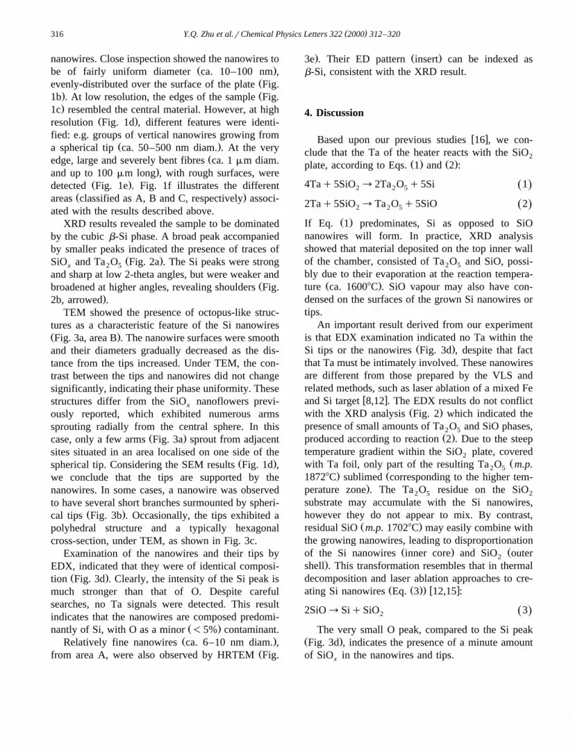
Ž . Ž . Ž .Fig. 3. TEM images a and b showing the octopus-like feature of the products, and c exhibiting the polygonal tip; d EDX patternŽ . Ž . Ž .revealing the dominance of Si; e very thin nanowires ca. 10 nm diam. , consisting of b-Si insert ED pattern .
( )Y.Q. Zhu et al.rChemical Physics Letters 322 2000 312–320316
nanowires. Close inspection showed the nanowires toŽ .be of fairly uniform diameter ca. 10–100 nm ,
Ževenly-distributed over the surface of the plate Fig.. Ž1b . At low resolution, the edges of the sample Fig..1c resembled the central material. However, at high
Ž .resolution Fig. 1d , different features were identi-fied: e.g. groups of vertical nanowires growing from
Ž .a spherical tip ca. 50–500 nm diam. . At the veryŽedge, large and severely bent fibres ca. 1 mm diam.
.and up to 100 mm long , with rough surfaces, wereŽ .detected Fig. 1e . Fig. 1f illustrates the different
Ž .areas classified as A, B and C, respectively associ-ated with the results described above.
XRD results revealed the sample to be dominatedby the cubic b-Si phase. A broad peak accompaniedby smaller peaks indicated the presence of traces of
Ž .SiO and Ta O Fig. 2a . The Si peaks were strongx 2 5
and sharp at low 2-theta angles, but were weaker andŽbroadened at higher angles, revealing shoulders Fig.
.2b, arrowed .TEM showed the presence of octopus-like struc-
tures as a characteristic feature of the Si nanowiresŽ .Fig. 3a, area B . The nanowire surfaces were smoothand their diameters gradually decreased as the dis-tance from the tips increased. Under TEM, the con-trast between the tips and nanowires did not changesignificantly, indicating their phase uniformity. Thesestructures differ from the SiO nanoflowers previ-x
ously reported, which exhibited numerous armssprouting radially from the central sphere. In this
Ž .case, only a few arms Fig. 3a sprout from adjacentsites situated in an area localised on one side of the
Ž .spherical tip. Considering the SEM results Fig. 1d ,we conclude that the tips are supported by thenanowires. In some cases, a nanowire was observedto have several short branches surmounted by spheri-
Ž .cal tips Fig. 3b . Occasionally, the tips exhibited apolyhedral structure and a typically hexagonalcross-section, under TEM, as shown in Fig. 3c.
Examination of the nanowires and their tips byEDX, indicated that they were of identical composi-
Ž .tion Fig. 3d . Clearly, the intensity of the Si peak ismuch stronger than that of O. Despite carefulsearches, no Ta signals were detected. This resultindicates that the nanowires are composed predomi-
Ž .nantly of Si, with O as a minor -5% contaminant.Ž .Relatively fine nanowires ca. 6–10 nm diam. ,
Žfrom area A, were also observed by HRTEM Fig.
. Ž .3e . Their ED pattern insert can be indexed asb-Si, consistent with the XRD result.
4. Discussion
w xBased upon our previous studies 16 , we con-clude that the Ta of the heater reacts with the SiO2
Ž . Ž .plate, according to Eqs. 1 and 2 :
4Taq5SiO ™2Ta O q5Si 1Ž .2 2 5
2Taq5SiO ™Ta O q5SiO 2Ž .2 2 5
Ž .If Eq. 1 predominates, Si as opposed to SiOnanowires will form. In practice, XRD analysisshowed that material deposited on the top inner wallof the chamber, consisted of Ta O and SiO, possi-2 5
bly due to their evaporation at the reaction tempera-Ž .ture ca. 16008C . SiO vapour may also have con-
densed on the surfaces of the grown Si nanowires ortips.
An important result derived from our experimentis that EDX examination indicated no Ta within the
Ž .Si tips or the nanowires Fig. 3d , despite that factthat Ta must be intimately involved. These nanowiresare different from those prepared by the VLS andrelated methods, such as laser ablation of a mixed Fe
w xand Si target 8,12 . The EDX results do not conflictŽ .with the XRD analysis Fig. 2 which indicated the
presence of small amounts of Ta O and SiO phases,2 5Ž .produced according to reaction 2 . Due to the steep
temperature gradient within the SiO plate, covered2Žwith Ta foil, only part of the resulting Ta O m.p.2 5
. Ž18728C sublimed corresponding to the higher tem-.perature zone . The Ta O residue on the SiO2 5 2
substrate may accumulate with the Si nanowires,however they do not appear to mix. By contrast,
Ž .residual SiO m.p. 17028C may easily combine withthe growing nanowires, leading to disproportionation
Ž . Žof the Si nanowires inner core and SiO outer2.shell . This transformation resembles that in thermal
decomposition and laser ablation approaches to cre-Ž Ž .. w xating Si nanowires Eq. 3 12,15 :
2SiO™SiqSiO 3Ž .2
The very small O peak, compared to the Si peakŽ .Fig. 3d , indicates the presence of a minute amountof SiO in the nanowires and tips.x

( )Y.Q. Zhu et al.rChemical Physics Letters 322 2000 312–320 317
Considering the various structures found in differ-Ž .ent areas Fig. 1 , we surmise that the temperature
gradient occurring at the outset may be responsiblefor such features, by influencing the nanowire growthrate. The largest temperature gradient occurs in zoneC, and the highest nanowire growth rate is achieved,
Ž .thereby leading to large fibres ca. 1 mm diam. . Inthis context, the marked growth rate seems to result
Ž .in highly defective nanowires Fig. 1e . By contrast,the smallest temperature gradient is found in zone A,resulting in the most regular nanowires. In zone BŽ .intermediate temperature gradient a moderategrowth rate results in larger smooth-surfacenanowires.
HRTEM measuments showed that the nanowiretips consist of well-crystallised Si, covered with a
Žthin amorphous SiO layer ca. 1–2 nm, xs1–2,x.Fig. 4a , according to the EDX results. However, no
obvious amorphous phase could be identified withinthe nanowires. By contrast with the tips, thenanowires were generally rather poorly crystallised,
Ž .with twinning and kink defects Fig. 4b . A notewor-thy feature of the nanowires is their more-or-less
Ž .constant tiprbody diameter ratio ca. 2 , althoughŽ .the tip sizes vary considerably Fig. 3b and c . This
ratio is fairly consistent with that found in the VLS-Ž . w xproduced nanowires typically ca. 1.5–2 5,6,16 .
As regards the Fe-catalysed Si nanowire growthŽ .generally involving a VLS step , the tip size ismainly determined by the initial size of the Feparticle, and the nanowire diameter is mainly con-
w xtrolled by the tip size 8 . In our case, we believe thatthe function of the in situ formed Si tip is, to some
Žextent, analogous to the metal catalysts Au, Fe or. ŽCo . The tips may also have experienced Si and.SiO accumulation andror extrusion stages during
nanowire growth, however their size is probablydetermined by the temperature. For example, whenthe temperature exceeds 13508C, the Si tip front willform a liquid phase by absorbing SiO or O – accord-ing to the Si–O phase diagram. Thus the highermelting points, associated with the Si and SiO2
phases, may cause extrusion from the Si tips, leadingto solid-phase nanowire growth. Because Ta has not
Žbeen involved in Si nanowire growth as verified by.EDX , it seems that the localised temperatures play
an important role in the experiments. It is obviousthat the temperature might affect the degree of Si
andror SiO vaporisation and migration. Further-more, the localised temperature also determines the
Žsizes of the initial Si tips formed from liquid phases.at temperature )14588C . The latter may further
alter some of the initial tip sizes by affecting thenanowire growth rates. In some cases, a low growth
Ž .rate was achieved as in zone B , indicating a high SiŽ .and SiO accumulation rate and a low extrusionrate, thus resulting in large tips. However, in zone C,
Žwhere the nanowire growth rate is highest i.e. high-.est extrusion rate , large nanowires were formed and
Žvery few tips were observed. In zone A where the.temperature gradient is lowest , because of its posi-
Žtion, accumulation is expected to be difficult reac-tion occurred only on the underside of the SiO2
.plate . Thus, low accumulation and extrusion results,Žleading to fine uniform tipless nanowires arrowed in
.Fig. 4b .Another interesting feature of these nanowires is
Žthat they exhibit directional crystal growth Fig. 4c,² :but not the 111 growth observed when the mate-
w x.rial is catalysed by Au 17 . As discussed above, thefunction of the Si tips is comparable with that ofmetal catalyst tips during the Si extrusion stage.Therefore, the growth axis of the nanowires is be-lieved to be associated with the crystal orientation ofthe Si tips. TEM analyses confirmed the crystallinestructure of the tips. In the XRD analyses, the high-angle diffraction peaks are broad and weak, withobviously shoulders. Because the tips are crystalline,the shoulders appear to arise mainly from thenanowires. Not only are the nanowires relativelypoorly crystalline, but they also occur in two typical
Ž .diameter distributions, i.e. ;10 nm zone A andŽ .)100 nm zone C . Poorly crystalline structures
may reduce the peak intensities and smallernanowires widen the peak profiles. Furthermore,since some nanowires were formed from the SiO
Ž Ž ..phase Eq. 3 , in these Si crystals, lattice deforma-tion may be retained if the transformation is not
Ž .complete O traces within the Si structures . Thismay be responsible for the shoulders on the peaks,which occur at high diffraction angles, due to thehigh-angle planes associated with long-distance crys-talline structures. This explanation is supported by
Ž .the HRTEM observations Fig. 4b .Because the tips and wires are of similar composi-
tion, the continuous accumulation of small amounts

( )Y.Q. Zhu et al.rChemical Physics Letters 322 2000 312–320318
Ž . Ž . ŽFig. 4. HRTEM images. a Massive Si tip covered with a very thin SiO layer indicated . The bottom right insert magnified from thex. Ž .upper white square shows the well-crystallised feature. The lattice fringes are separated by ca. 0.31 nm, consistent with b-Si; b kinkŽ .defective structure; c different growth directions of the nanowires.

( )Y.Q. Zhu et al.rChemical Physics Letters 322 2000 312–320 319
Ž .Fig. 5. A schematic model for Si nanowire growth. a Nano- orŽ . Ž .micro-Si tips formed. b Initial nanowire formation. c Adjacent
Ž .site growth, or alternatively, d Coalescence.
of SiO during growth may facilitate the joining ofone nanowire to another nanowire tip, leading tostructures shown in Fig. 3b. Meanwhile, different
Ž .extrusion sites nucleation sites for the nanowiresŽmay occur at the Si tip surface due to the polyhedral
. Ž .structure , octopus-like structures result Fig. 3a .These processes are comparable with Co coalescenceor bifurcation, which provides the main driving force,
w xfor the formation of SiO nanoflowers 6,16 . Thex
primary driving force for Si nanowire growth ap-pears to lie in the temperature gradients, which resultin products, rather different from the 3-D nanoflow-
Ž .ers. In view of the SEM results Fig. 1d , we con-clude that the tips are supported by the nanowires. Itis apparent that only a few arms sprout from adjacentsites situated in a localised area of the spherical tipŽ .Fig. 3a , and that some nanowires have several short
Ž .branches surmounted by larger tips Fig. 3b .Based on the above observations, we propose a
Ž . Ž . Žmodel Fig. 5 for Si nanowire growth. a Si Eq.Ž ..1 accumulates to form nano- or micro- particles onthe lower temperature upper surface of the SiO2
Ž . Ž Ž ..plate. b The resulting SiO Eq. 2 accumulates onŽ .the Si particle surface. c Si extrudes from this
Ž .particle, initiating nanowire growth. d In severaladjacent sites extrusion occurs leading to octopus-like
Ž . Ž .structures Fig. 3a , or alternatively, e a nanowire
attaches to another particle, thus generating linkedstructures of the type shown in Fig. 3b.
5. Conclusions
Octopus-like structures consisting of metal-freecubic Si nanowires and attached Si nanoparticleshave been generated in good yield, by heating a SiO2
plate on Ta at ca. 16008C under Ar. HRTEM obser-vations reveal that the Si nanowires contain kinksand twinning defects, whereas their tips are generallywell-crystallised and covered with a distinct amor-
Ž .phous SiO xs1–2 thin layer. The effect of thex
temperature gradient is believed to be the primaryreason for nanowire and nanostructure growth. Anon-metal-catalysed mechanism has been proposedto account for the facts.
Acknowledgements
We thank the Royal Society, the JFCC, Conacyt-Ž .Mexico and DGAPA-UNAM IN 107-296 HT , EP-´
Ž .SRC, and Max-Planck Society Fellowship BQWfor financial support. We are grateful to J. Thorpe
Ž .and D. Randall Sussex for assistance with TEMand SEM facilities.
References
w x Ž .1 A.P. Alivisatos, Science 271 1996 933.w x2 D.P. Yu, Q.L. Huang, Y. Ding, H.Z. Zhang, Z.G. Bai, J.J.
Wang, Y.H. Zou, W. Qian, G.C. Xiong, S.Q. Feng, Appl.Ž .Phys. Lett. 73 1998 3076.
w x3 H.I. Liu, N.I. Maluf, R.F.W. Pease, J. Vac. Sci. Tech. B 10Ž .1992 2846.
w x Ž .4 R.S. Wagner, W.C. Ellis, Appl. Phys. Lett. 4 1964 89.w x5 J. Westwater, D.P. Gosain, S. Usui, Phys. Status Solid
Ž .A-Appl. Res. 165 1998 37.w x6 Y.Q. Zhu, W.K. Hsu, M. Terrones, N. Grobert, H. Terrones,
J.P. Hare, H.W. Kroto, D.R.M. Walton, J. Mater. Chem. 8Ž .1998 1859.
w x7 Y.Q. Zhu, W.B. Hu, W.K. Hsu, M. Terrones, N. Grobert, T.Karali, H. Terrones, J.P. Hare, P.D. Townsend, H.W. Kroto,
Ž .D.R.M. Walton, Adv. Mater. 11 1999 844.w x Ž .8 A.M. Morales, C.M. Lieber, Science 279 1998 208.

( )Y.Q. Zhu et al.rChemical Physics Letters 322 2000 312–320320
w x Ž .9 G.W. Zhou, Z. Zhang, D.P. Yu, J. Cryst. Growth 197 1999129.
w x10 Y. Zhang, K. Suenaga, C. Colliex, S. Iijima, Science 281Ž .1998 973.
w x11 G.W. Meng, L.D. Zhang, Y. Qin, F. Phillipp, S.R. Qiao,Ž .H.M. Guo, S. Y Zhang, Chin. Phys. Lett. 15 1998 689.
w x12 N. Wang, Y.H. Tang, Y.F. Zhang, C.S. Lee, I. Bello, S.T.Ž .Lee, Chem. Phys. Lett. 299 1999 237.
w x13 H. Dai, E.W. Wong, Y.Z. Lu, S.S. Fan, C.M. Lieber, NatureŽ .375 1995 769.
w x Ž .14 W.Q. Han, S.S. Fan, Q.Q. Li, Y.D. Hu, Science 277 19971287.
w x15 N. Wang, Y.F. Zhang, Y.H. Tang, C.S. Lee, S.T. Lee, Appl.Ž .Phys. Lett. 73 1998 3902.
w x16 Y.Q. Zhu, W.K. Hsu, M. Terrones, N. Grobert, W.B. Hu,J.P. Hare, H.W. Kroto, D.R.M. Walton, H. Terrones, Chem.
Ž .Mater. 11 1999 2709.w x17 J. Westwater, D.P. Gosain, S. Tomiya, S. Usui, J. Vac. Sci.
Ž .Tech. B 15 1997 554.