Molecular nanostructures on ferromagnetic metals for ...
242
Molecular nanostructures on ferromagnetic metals for spintronics Instituto de Ciencia Molecular Universitat de Valencia Memoria presentada por Michele Mattera para aspirar al grado de Doctor en Nanociencia y Nanotecnologia Septiembre 2017 Directores : Prof. Eugenio Coronado Miralles Dra. Alicia Forment Aliaga Dr. Sergio Tatay Tutor Dra. Alicia Forment Aliaga
-
Upload
khangminh22 -
Category
Documents
-
view
7 -
download
0
Transcript of Molecular nanostructures on ferromagnetic metals for ...

Molecular nanostructures on
ferromagnetic metals for spintronics
Instituto de Ciencia Molecular
Universitat de Valencia
Memoria presentada por Michele Mattera para aspirar al grado de Doctor en Nanociencia y Nanotecnologia
Septiembre 2017
Directores :
Prof. Eugenio Coronado Miralles
Dra. Alicia Forment Aliaga
Dr. Sergio Tatay
Tutor
Dra. Alicia Forment Aliaga


D. EUGENIO CORONADO MIRALLES, catedratico del Departamento de Química
Inorgánica de la Universitat de Valencia, Dña. ALICIA FORMENT ALIAGA
doctora por la Universitat de Valencia y actualmente investigadora en el
Instituto de Ciencia Molecular de la Universitat de Valencia y D. SERGIO TATAY,
doctor por la Universitat de Valencia y actualmente investigadora en el
Instituto de Ciencia Molecular de la Universitat de Valencia,
CERTIFICAN:
Que la memoria presentada por D. Michele Mattera con titulo: Molecular
nanostructures on ferromagnetic metals for spintronics corresponde a su Tesis
Doctoral y ha sido realizada bajo su dirección en el Instituto de Ciencia
Molecular, autorizando mediante este escrito la presentación de la misma para
optar al grado de Doctor.
En Paterna, a 26 de Septiembre de 2017
Prof. Eugenio Coronado Miralles Dra Alicia Forment Aliaga
Dr Sergio Tatay Michele Mattera


1. When a distinguished but elderly scientist states that
something is possible, he is almost certainly right. When
he states that something is impossible, he is very
probably wrong.
2. The only way of discovering the limits of the possible is
to venture a little way past them into the impossible.
3. Any sufficiently advanced technology is indistinguishable
from magic.
Arthur C.Clarke ‘ Laws


to my wife MaFe,
my parents Paola and Salvatore,
and my grandparents.


i
Table of Contents
Acknowledgements ................................................................................................ v
Motivation and organization of this thesis ............................................................ix
Abbreviations ......................................................................................................... xiii
List of publications ................................................................................................ xv
List of Figures........................................................................................................ xvii
List of Tables ....................................................................................................... xxvii
1. Introduction ...................................................................................................... 1
1.1 Self-assembled monolayers for surface functionalization ..................... 1
1.2 Characterization techniques ................................................................... 5
1.3 Application of SAMs ............................................................................... 12
1.4 SAMs application in spintronics ............................................................. 16
1.4.1. Basis of Spintronics ........................................................................ 16
1.4.2. Molecular Spintronics ..................................................................... 19
1.4.3. SAMs in spintronics ....................................................................... 20
1.5 References .............................................................................................. 23
2. Self-assembled monolayers on Permalloy ................................................... 39
2.1. Introduction ........................................................................................... 39
2.2. Results and discussion .......................................................................... 42
2.2.1. Influence of the surface pre-treatment ....................................... 42
2.2.1 Preparation of SAMs ..................................................................... 47
2.2.2 Structural Characterization ........................................................... 54
2.2.3 Magnetic characterization of modified substrates ..................... 66
2.2.4 APA SAMs Applications ................................................................. 69
2.3 Conclusions ............................................................................................. 72
Table of Contents
ii
2.4. References ............................................................................................. 74
3. Functionalization of metallic ferromagnetic surfaces .................................. 81
3.1. Introduction ............................................................................................ 81
3.2. Results and discussion .......................................................................... 88
3.2.1. Wet chemical etching studies ....................................................... 88
3.2.2. Formation of the SAM .................................................................. 102
3.2.3. Advanced characterization of C12S SAM ...................................... 106
3.2.4. Extending the functionalization .................................................. 110
3.2.5. Fabrication of MTJ devices based on FM electrodes and SAMs . 112
3.3. Conclusions ........................................................................................... 114
3.4. References ............................................................................................. 115
4. Characterization of lamellar alkanethiolate domains on ferromagnetic
surfaces ................................................................................................................. 119
4.1. Introduction .......................................................................................... 119
4.2. Results and discussion ......................................................................... 123
4.2.1. Structural Studies ......................................................................... 123
4.2.2. Area distribution studies .............................................................. 134
4.2.3. Spectroscopy studies ................................................................... 139
4.2.4. Growth rate studies ...................................................................... 143
4.2.5. Temperature and humidity influence studies ............................. 152
4.2.6. Etching Experiments .................................................................... 157
4.2.7. Growth mechanism ...................................................................... 158
4.3. Conclusions ........................................................................................... 160
4.4. References ............................................................................................ 162
Conclusions and Outlook ..................................................................................... 169

Table of Contents
iii
Experimental Methods ......................................................................................... 173
I. Reagents ................................................................................................... 173
II. Substrate Preparation .............................................................................. 173
III. General procedure for SAM Formation ............................................... 174
III.1. Alkylphosphonic Acid Monolayer Formation ...................................... 174
III.2. Alkanethiol Monolayer Formation ....................................................... 175
IV. Characterization Techniques ............................................................... 176
IV.1. X-ray Photoelectron Spectroscopy (XPS) ........................................... 176
IV.2. Contact Angle (CA) measurements ..................................................... 176
IV.3. Atomic Force Microscopy (AFM) ......................................................... 177
IV.4. Scanning Electron Microscopy (SEM) ................................................. 177
IV.5. Optical Microscopy ............................................................................... 177
IV.6. Matrix-Assisted Laser Desorption Ionization- Time of Flight Mass
Spectrometry ( MALDI-TOF MS) ...................................................................... 177
IV.7. Infrared Reflection- Absorption Spectroscopy (IRRAS) ..................... 178
IV.8. X-Ray Reflectivity (XRR) ....................................................................... 178
IV.9. Magneto-Optical Kerr Effect Magnetometry (MOKE) ....................... 179
IV.10. Auger Spectroscopy (AES) ............................................................... 179
IV.11. Raman Spectroscopy ........................................................................ 179
IV.12. X-ray Absorption Spectroscopy (XAS) and X-Ray Magnetic
Dichroism (XMCD). ........................................................................................... 180
V. Microcontact Printing and Etching .......................................................... 181
VI. Inverted Lithography ........................................................................... 182
Appendix ............................................................................................................... 183
A.1 Atomic Force Microscopy (AFM) ......................................................... 183

Table of Contents
iv
A.2 Infrared Reflection Absorption Spectroscopy (IRRAS) ...................... 185
A.3 X-Ray Reflectivity (XRR) ....................................................................... 186
A.4 References ............................................................................................ 189
Resumen en castellano ........................................................................................ 191

v
Acknowledgements
The road to accomplish the title of PhD is long, but the path is made of a large
number of people, that I will divide in different groups, to which I would
express my thankfullness personally.
The first group, is the one of the directors: Prof. Eugenio Coronado, Dra Alicia
Forment and Dr Sergio Tatay. The three of them have been so important during
these years with their enduring support, talks about problems, and
brainstormings to reach the new frontiers in organic and molecular spintronics.
I would like to thank Prof Eugenio Coronado, for welcoming in his group to
develop my PhD. For my supervisors Alicia and Sergio, I would like to thank
them, for their ideas to solve especially the organization of chapter 4, that still
remains an interesting work with some open issues.
A special thank goes to my parents, Paola and Salvatore, with their endless
support you gave me the motivation, along these years, to pursue my ambition
to obtain a PhD degree in Nanoscience, even if you are not so familiar with this
theme.

vi
I want to give a special thank to my wife, Mafe, who waited for me to finish and
helped me maintaining clear my focus and motivation to achieve the best
results as possible.
An important group is made by the people which were not in the lab, but mean
very much to me: my wife and mine cousins, Elisabetta, Guglielmo, Alessandro,
Erika which had always a joke to help me relax during the holidays (easter,
summer or Christmas).
The lab people group with which I spent so many hours together, in different
aspects : from longer measurements sessions in the lab with different
equipments, like Ramon, Garin, Victor in the AFM lab, with music and jokes,
Marc with Raman, who has so many patience to obtain the best conditions for
the measurement. The technicians, Angel, Jose, Eva, who supported me in the
routine of the lab. There were also people that supported me outside the lab,
like the people who already finished their thesis but were up to join in social
dinners, or simply having a refreshing beer in the plaza de los negritos, in the
city center. These people are Mauri, who was also my bestman, David, Jorge,
Maria and all the others mentioned before.
I would like to thank the all the people from the office 2.10.1-3: Efren, Julia,
Elena, Yoan, Juan Pablo, Walter, Sara, Samuel y Ramon, Marco and Manel. With
you I could balance the long days with some jokes, while smoking outside and
drinking a coffee, and we also talked about chemistry, physics, and all the
wonderful hidden in the quantum world.

vii
All of you are so important to the ultimate goal of a PhD Thesis, the possibility
to create a network that will persist also when the thesis ends, and I hope will
support me for years.
I would also thank the eventual reader, which will find all the information to
repeat my experiments, and in the case it helps to motivate him/her to do a
PhD, I hope he/she will improve my work and maybe obtain something
interesting from it.

viii

ix
Motivation and organization
of this thesis
The main goal that motivated the development of this thesis was the
preparation of new protocols to functionalize room temperature
ferromagnetic materials by means of the formation of self-assembled
monolayers (SAMs). We pursued to create inorganic/organic interfaces through
strategies that i) are cheap and easily applicable in a chemistry lab; ii) do not
degrade the magnetic nature of the underlying substrate; iii) lead to high-
quality, oxide free interfaces like those needed when the interface is
implemented in spintronic devices. Therefore, metals and alloys such as cobalt
and permalloy, which magnetization and spin polarization properties persist at
room temperature and have been widely used in spintronics, have been our
focus of study.
This manuscript is divided in four main chapters:
In Chapter 1 a brief introduction to the concept of SAMs is presented. First, we
will discuss the chemical groups commonly chosen to functionalize different
kinds of surfaces, then, we will summarize the surface characterization

Motivation and organization of this thesis
x
techniques usually applied to study these SAMs. Finally, a brief summary of
SAMs most common applications will be presented.
Chapter 2 is focused on the functionalization of permalloy through the
attachment of the molecular units to its passivating oxide layer. We will present
a strategy that combines hydrogen plasma treatment, to increase the oxide
reactivity and wet chemistry to form high quality SAMs of alkylphosphonic
acids (APAs). We will also show how microcontact printed SAMs can be
successfully prepared and that they can be used as efficient etch resistant
layers.
In Chapter 3 a new protocol to recover already passivated ferromagnetic
metals is presented. We will pursue a selective removal of the oxide layer
without damaging the metallic bulk and compatible with lithographic
techniques used in modern spintronic device production. The method
presented here can be used to allow the preparation of SAMs directly on the
ferromagnetic metallic surface. At the end of the chapter, we will briefly
discuss how these hybrid interfaces composed of SAM and metal have been
successfully integrated in magnetic tunnel junctions that are able to work at
room temperature.
During the development of chapter 3, we observed the appearance of discrete
lamellar domains on the surface of alkanethiolate modified ferromagnetic
surfaces when they were exposed to air. This spontaneous effect had been
never reported before. In chapter 4, we present a detailed study of these
domains by means of different surface characterization techniques that

Motivation and organization of this thesis
xi
permitted us to follow the growing process in real time and unravel the metal
organic nature of these lamellar structures.
Finally, we summarize the general conclusions that can be extracted from the
research results reported in this thesis as well as the future perspectives, along
with some questions that in our opinion still remain open, but that we expect
to tackle in the future.
At the end of the manuscript, we have included a specific section that describes
the experimental methods used and developed during this work. Moreover, we
have included an appendix that explain in more detail some specific
characterization techniques, such as AFM, XRR and IRRAS, used thorough the
development of this thesis. We hope that this information will help those not
familiar with them to better follow the results presented here.

xii

xiii
Abbreviations
µCP Microcontact printing
AES Auger electron spectroscopy
AF Antiferromagnetic
AFM Atomic force microscopy
Alq Tris(hydroxyquinoline)aluminium(III)
AMR Anisotropic magnetoresistance (AMR)
APAs Alkylphosphonic acids
CD Compact disc
Co Cobalt
CoFeB Cobalt Iron Boron
Fe Iron
FM Ferromagnetic
GA Glycolic acid
GIXRD Grazing incidence X-ray diffraction
GMR Giant magnetoresistance effect
IRRAS Infrared reflection absorption spectroscopy
ITO Indium tin oxide
LBL Layer-by-layer
LDHs Layered double hydroxides
LEDs Light emitting diodes
LMAs Lamellar Metal-alkanethiolates
LSMO Lanthanum Strontium Manganite Oxide
MALDI-TOF Matrix assisted laser desorption/ionization time of flight
MOKE Magneto-optical Kerr effect

Abbreviations
xiv
MRAM Magnetoresistive random-access memories
MTJ Magnetic tunnel junction
ND Neutral-density filter
Ni Nickel
Py NiFe alloy or Permalloy
OFETs Organic field effect transistors
OLEDs Organic light emitting diodes
PDMS Polydimethylsiloxane
SAES Scanning Auger electron spectroscopy
SAMs Self-assembled monolayers
surMOF Surface metal organic framework
SV Spin-valve
T slab thickness
T6 Sexithienyl
TMDCs Transition metal dichalcogenides
TMR Tunnel magneto resistance
TOF-SIMS Time of flight secondary ions mass spectrometry
TS Template stripping
wθAA Water advancing contact angle
wθCA Water contact angle
wθRA Water receding contact angle
XAS X-ray absorption spectroscopy
XMCD X-ray magnetic circular dichroism
XPS X-ray photoelectron spectroscopy
XRR X-ray reflectivity
ρ Density of the material in the slab

xv
List of publications
1. Michele Mattera, Ramón Torres-Cavanillas, Juan Pablo Prieto-Ruiz,
Helena Prima-Garcia, Sergio Tatay, Alicia Forment-Aliaga and
Eugenio Coronado, Self-Assembled Monolayers on a Ferromagnetic
Permalloy Surface. Langmuir 31, 5311–5318 (2015).
2. Marta Galbiati, Sophie Delprat, Michele Mattera, Samuel Mañas-
Valero, Alicia Forment-Aliaga, Sergio Tatay, Cyrile Deranlot, Pierre
Seneor, Richard Mattana and Frédéric Petroff, Recovering
ferromagnetic metal surfaces to fully exploit chemistry in molecular
spintronics. AIP Adv. 5, 57131 (2015).
3. Michele Mattera, Marta Galbiati, Sergio Tatay, Alicia Forment-Aliaga
and Eugenio Coronado, Spountaneous formation of lamellar island
domains on ferromagnetic surfaces (manuscript in preparation).

List of publications
xvi
4. Víctor Rubio-Giménez, Marta Galbiati, Javier Castells-Gil, José
Navarro-Sánchez, Garín Escorcia-Ariza, Michele Mattera, Thomas
Arnold, Jonathan Rawle, Sergio Tatay, Eugenio Coronado and Carlos
Martí-Gastaldo, Bottom-up fabrication of conductive Metal-Organic
Frameworks ultrathin films (manuscript submitted)
xvii
List of Figures
Chapter 1
Figure 1 - Pictorial representation of the structure of a SAM highlighting its different
parts and its properties. ......................................................................................... 2
Figure 2 – Schematic representation of the dynamic sessile drop method : a) wθAA: a
constant volume of water is added to the first drop till reaching a plateau. b) wθRA:
a constant volume of water is removed from the drop till reaching a plateau. .. 7
Figure 3 - AFM images of mica functionalized with alkanephosphonic acid at different
stages of the SAM formation. The evolution from discrete domains to a complete
monolayer can be observed. Figure reproduced from ref 35. .............................. 8
Figure 4 – Schematic representation of the microcontact printing and wet-chemical
etching processes used to microstructure < 1 µm Si features. Figure reproduced
from reference 85. .................................................................................................. 14
Figure 5 - Schematic cross-section representation of bottom–gate top–contact OFETs
integrating a SAM that plays different roles: (a) gate dielectric primer, (b) molecular
dielectric, (c) organic semiconductor and (d) electrode modifier. Figure adapted
from reference 93 ................................................................................................... 15
Figure 6 - Pictorial representation of a Resistance vs Magnetic Field (R(H))
measurements in a generic spintronic device: a) The magnetization in both
electrodes is parallel, resulting in a low resistance; b) the magnetic field is swept till
the magnetization of one of the electrodes (the softer one) changes its orientation,
resulting in an antiparallel configuration, characterized with a higher resistance; c)
the magnetic field is swept till the magnetization of the other electrode (the harder
one) changes, returning to a parallel configuration, resulting again in low resistance

List of Figures
xviii
and d) the cycle is closed by sweeping the magnetic field in the reverse direction to
return to a). ............................................................................................................. 17
Figure 7 - a) Scheme of the MTJ used by Petta. b) R(H) measurement done at 4.2 K with
5 mV bias, showing 16% of TMR. Figure adapted from reference 107. ................. 21
Figure 8 - a) Scheme of the MTJ used by Wang. b) R(H) measurement done at 4.2 K with
10 mV bias, showing 10% of TMR. Figure adapted from reference 108. ............... 21
Figure 9 - a) Scheme of the MTJ used by Galbiati et al. . b) R(H) measurement done at 4
K at different bias voltages: 10 mV (red), 800 mV (orange) and 2 V (blue). Figure
adapted from reference 111. ................................................................................... 22
Chapter 2
Figure 1 - XPS survey spectra of 40 nm air exposed Py sample (red) and after Ar+ milling
(grey). ...................................................................................................................... 43
Figure 2 - High-resolution XPS spectra at the Ni2p3/2 (a) and Fe3p3/2 (b) edges of Py
films subjected to different treatments: Ar+ milling (reference, gray), air oxidation
(no plasma, red), H2 plasma (black), O2 plasma (blue). ....................................... 44
Figure 3 - Top: Deconvoluted high-resolution O1s XPS spectrum of an air oxidized Py film
(red line) without any additional plasma treatment. Bottom: The upper spectrum is
compared with those of Py films subjected to H2 (black) and O2 (blue) plasmas. 45
Figure 4 – a) XRR reflectograms of Py surface subjected to different treatments: bare
sample (red dots), H2 plasma (black dots) and O2 plasma (blue dots). b) Model used
to fit the curves. ...................................................................................................... 46
Figure 5 - AFM topographic images (1x1 µm2) of Py substrates after different plasma
treatments: a) air oxidized Py substrate, b) Weak H2 Plasma, c) Strong H2 Plasma, d)
Weak O2 Plasma, e) Strong O2 Plasma. ................................................................. 47

List of Figures
xix
Figure 6 - Coverage as a function of time for a Py substrate functionalized with 2 mM
C12P (solid circle) and C18P (hollow circle) 2-propanol solutions. Data have been
fitted to a biexponential Langmuir isotherm (dashed red line). .......................... 50
Figure 7 - SAM growth models: a) Uniform growth model: a complete monolayer is
formed and the thickness increases synchronously as a function of time (i-ii). b)
Island-like growth model: the molecules arrange themselves into discrete domains:
(i) when two domains come in contact, coalescence takes place forming a bigger
domain, which continues to grow until a complete monolayer is formed (ii). The
thickness is maintained through the self-assembly. ............................................. 52
Figure 8 – (a-f) AFM images of a functionalized Py substrate with C18P took at different
times. ....................................................................................................................... 54
Figure 9 - AFM topographic images (1x1 µm2) of H2 plasma treated Py substrates: a)
neat solvent, b) C12P SAM, c) C14P SAM, d) C16P SAM, e) C18P SAM. ................. 55
Figure 10 - MALDI-TOF spectra measured for C12P (Mw=250.31), C14P (Mw=278.37) and
C16P (Mw=306.42) SAM-functionalized Py substrates. ........................................ 56
Figure 11 - IRRAS spectra of the region corresponding to the alkyl C-H stretching. C12P
(red) and C18P (black) SAM-functionalized substrates. Vertical gray lines are a
reference for the eye and mark the position of C18P methylene vibrations. ...... 58
Figure 12 - Data analysis of the IRRAS measurements: (a) Position of the C-H bond
antisymmetric strecth for alkylphosphonic acids of different chain length. (b)
Estimated chain tilt angle (α) with respect to the surface normal of alkyl phosphonic
acids of different chain length. (c) Estimated thicknesses from IRRAS spectra of
monolayers with different chain length (black dots) and calculated thicknesses for
vertical aligned all trans configuration (gray dots). .............................................. 59
Figure 13 - Sketch of an alkylphosphonic acid anchored to the surface through a
tridentate binding. Angles and bond distances used to estimate the theoretical
thickness of a SAM are included. ........................................................................... 61

List of Figures
xx
Figure 14 - a) XRR reflectograms of Py surface subjected to H2 plasma (black dots) and
then functionalized with CnP : C12P (pink dots), C14P (orange dots), C16P (green
dots) and C18P (purple dots). b) Model used to fit the curves (solid lines in (a)). 61
Figure 15 - P2p3/2 XPS spectra of: (a) bare Py substrate. (b) C18P SAM on Py. ......... 64
Figure 16 - Relative thickness of APA monolayers formed on Py as determined from XPS,
XRR and IRRAS. ....................................................................................................... 65
Figure 17 - Preparation of the different samples used for the MOKE measurements. 67
Figure 18 - Low temperature (top) vs room temperature (bottom) magnetization
(measured using MOKE technique) recorded for a non-oxidized gold-capped Py
sample (Capped) and air oxidized (Bare), pre-treated with hydrogen plasma (H2),
pre-treated with hydrogen plasma and APA functionalized (SAM) and pre-treated
with oxygen plasma (O2) samples. ........................................................................ 68
Figure 19 - Friction AFM image of 15 µm2 of C18P SAM stripes patterned on a ~16 nm
thick Py substrate, taken before etching. b) Topographic AFM image of sample
showed in (a) after the etching treatment. c) Height profile corresponding from the
blue line in (a) and the red line in (b). .................................................................... 71
Chapter 3
Figure 1 – Schematic representation of the fabrication of SAM-based spintronic devices.
a) UHV route : i) bottom electrode deposition; ii) SAM formation; iii) top electrode
deposition. b) UHV + GB route: i) bottom electrode deposition; ii) SAM formation in
inert atmosphere; iii) top electrode deposition. c) Alternative route: i) bottom
electrode deposition; ii) air exposure and oxide formation; iiia) oxide removal and
SAM formation (iiib) in inert atmosphere; iv) top electrode deposition. ............ 84
List of Figures
xxi
Figure 2 – Co sample treated with hydrazine: a) XRR reflectograms before and after the
treatment. b) Topographic AFM image of the surface taken after the treatment. c)
Model used to fit the reflectograms in a. .............................................................. 89
Figure 3 - Etching studies on Co samples: a) Reflectograms of Co-Ox samples exposed
to GA for different times under ambient conditions (approach A). b) Co thickness
measured in Co samples exposed to GA etching following different approaches:
etching performed inside a glove box (Co-GB, approach B, black), and (Co-GB
stepped, approach C, blue). c) Topographic AFM image under ambient conditions of
a Co sample after 26 minutes of etching inside the glove box (Co-GB). .............. 90
Figure 4 - Reflectograms of Co-Ox samples exposed to GA with different
concentrations: reference (black), 10% (light green), 5% (orange), 1% (blue) and 0.5%
(red). ........................................................................................................................ 92
Figure 5 – a) Topographic AFM images measured under ambient conditions of air
oxidized Co surfaces exposed to GA etching solutions in GB for different amounts of
time. b) Pictorial representation of the Co oxide etching process, as a function of
time. ......................................................................................................................... 94
Figure 6 - a) Topographic AFM image of the patterned Co stripes on silicon surface. b)
Topographic profile of two zones of the patterned stripes, before and after the GA
etching. The difference between the two profiles is of 2 nm. .............................. 95
Figure 7 - Set of samples used for XPS and SQUID characterization: Co-UHV (red) was
completely produced under UHV atmosphere. Co-Ox (blue) was exposed to air and
then capped with gold. Co-GA (black) was exposed to air, treated with GA inside the
glove box and then capped with gold without breaking the inert atmosphere. 96
Figure 8 - XPS spectra of O1s (a-c) and Co2p (d-f) of Co samples subjected to different
treatments: Co-UHV (red) was completely produced under UHV atmosphere. Co-Ox
(blue) was exposed to air and then capped with gold. Co-GA (black) was exposed to
air, treated with GA inside the glove box and then capped with gold without
breaking the inert atmosphere. ............................................................................. 97

List of Figures
xxii
Figure 9 - SQUID characterization of Co samples subjected to different treatments: Co-
UHV (red) was completely produced under UHV atmosphere. Co-OX (blue) was
exposed to air and then capped with gold. Co-GA (black) was exposed to air,
treated with GA inside the glove box and then capped with gold without breaking
the inert atmosphere. ............................................................................................. 98
Figure 10 – a) XRR reflectograms of Py samples subjected to different GA etching times
in air. b) Comparison of the thickness evolution with etching time for Py samples
treated with GA inside a glove box (black) and in ambient atmosphere (red). . 100
Figure 11 - XPS spectra at the O1s (a-c) and Ni2p (d-f) edges of Py samples subjected to
different treatments: UHV (red), oxidized (Ox) (blue), etched GA (black). ........ 101
Figure 12 - Coverage as a function of time for Co substrate functionalized with C12S
SAM. ........................................................................................................................ 104
Figure 13 – Topographic AFM images of: C12S functionalized samples Co (a) and Py (b)
after 16 hours of reaction taken inside the glove box. The images were FT filtered to
remove the 50 Hz electrical noise from the GB. .................................................... 105
Figure 14 - IRRAS spectrum of a C12S SAM on Py. From left to right the asymmetric
methylenes and methyl vibrations and the correspondent symmetric ones. ..... 106
Figure 15 – XAS spectra recorded at Fe-L2,3 (a) and Ni-L2,3 (b) edges with left
polarization (red) and right polarization(black) of a stacked Py//C12S/Co/Al sample
after glycolic acid treatment and functionalization with C12S. ............................ 108
Figure 16 - XMCD-PEEM images recorded at Co, Fe and Ni L3 edges. ........................ 109
Figure 17 - AFM topographic images of Co functionalized with: a) C12S, b) C14S, c) C16S
and d) C18S. The scale bar is 5 µm. ......................................................................... 111
Figure 18 - Nanoindentation process for the preparation of a Py//SAM/Co MTJ: (i)
deposition of photoresist, (ii) fabrication of nanoholes, (iii) etching of the oxide and
functionalization of the metallic surface and (iv) top electrode deposition. ...... 113

List of Figures
xxiii
Figure 19 - Electrical characterization of the fabricated junction (Py//C16S/Co/Al): a) I-V
curve that demonstrates the tunneling regime and b) R-H that shows TMR at room
temperature. ........................................................................................................... 113
Chapter 4
Figure 1 – a) Pictorial representation of island-like domain formation on an alkanethiol
functionalized FM sample: i) Etching of native oxide layer on the FM with GA, ii)
grafting of the CnS SAM, iii) functionalized films stable under inert atmosphere, iv)
islands grow as the sample is exposed to air. b-c) Optical images of a functionalized
Co surface with C14S just after functionalization (b) and after 16h of air exposure
(c). ............................................................................................................................ 120
Figure 2 - Combined Optical - AFM characterization of a functionalized Co-C14S sample:
a) Optical microscopy. b) AFM topographic image and c) height distribution of b. 121
Figure 3 - Figure extracted from reference 23, which displays the formation of LMAs
from silver nanoparticles. ....................................................................................... 122
Figure 4 - SEM image of a Ag(CnS) LMA extracted from ref 8 (n = 16). Cartoon
representing the structure of a M(SR)2 lamellar metal-alkanethiolate. The thickness
of a single LMA slab is the result of the contributions from the methylene chain
(dCH2), terminal methyl group (dCH3), carbon-sulfur (dC-S) and metal-sulfur (dSap) bond
distances. ................................................................................................................. 122
Figure 5 - AFM topographic images and height distribution profiles of islands obtained
with C14S (a and d), C16S (b and e) and C18S (c and f). The difference between the
black lines corresponds to the step heights. The scale bar is of 5 µm. ................ 124
Figure 6 – a) Step height versus chain length of M-CnS island domains determined from
AFM (red dots, M = Co and Py) and XRD (blue dots, M = Co). Solid lines are linear fits
to the data (SH = mC + b, C = number of carbons). Fitted values are displayed as an

List of Figures
xxiv
inset. b) Step height distribution obtained after measuring individual step heights in
6 islands of each chain length on Co and Py. AFM error bars in a) are calculated as
Gaussian fit from b). The error bars for XRD were calculated from the average of at
least 2 different XRD measurements as those displayed in Figure 7. ................... 125
Figure 7 – Out-of-plane XRD measurements on Co-CnS samples: C14S (red), C16S (black)
and C18S (blue). ...................................................................................................... 126
Figure 8 - AFM height statistics of island features: C14S(red), C16S (black) and C18S
(blue). Yellow dashed line corresponds to the integral of the histogram. .......... 128
Figure 9 – a) Top view of a schematic representation of the metal-sulfur regions. Metal
atoms are represented in red, sulfur atoms above and below the backbone plane
are in yellow and b) octahedral coordination of the metal atom. ....................... 132
Figure 10 - AFM images of islands grown on Co from different alkanethiolates with their
respective height histogram: C18S (a-d) , C16S (b-e) and C14S (c-f). The scale bar is of
5 µm. ........................................................................................................................ 134
Figure 11 – A C14S island on Py imaged with different techniques a) AFM, b) Optical
Microscope, c) Optical Microscope with ND Filter and d) SEM. ........................... 135
Figure 12 - Representative 100x optic images of Co and Py functionalized samples. 136
Figure 13 - Optical domain area histograms of Co and Py samples functionalized with
C14s, C16S and C18S. Yellow dashed line is the area integral. ............................... 137
Figure 14 - Auger spectra determined inside (red) and outside (green) a C14S island
grown over a 15 nm Co substrate, b) the height profile of the measured zone.
Elemental spectra of c) Cobalt, d) Oxygen and e) Sulphur. The scale bar is of 2 µm.
................................................................................................................................. 141
Figure 15 - Raman spectra recorded inside and outside an island, with its insets i), ii) and
iii) of the regions of interest. Peaks marked with an * come from the silicon
substrate. ................................................................................................................ 143
Figure 16 - Real time growth of C18S-Co island domains, imaged with AFM: AFM
topographic images at 20 min (red), 2.5 h (orange), 5 h (yellow), 8 h (light green),

List of Figures
xxv
14.75 h (light blue), 15h (blue), 16.75 h (purple) and 20.65 h (deep red). (a) Evolution
of the island coverage with time and (b) evolution of the height profile with time.
................................................................................................................................. 144
Figure 17 - Real time growth of C14S-Co island domains, imaged with AFM: AFM
topographic images at 10 min (red), 1 h 10 min (blue), 2 h 20 min (orange), 3 h (dark
green), 5 h 40 min (light blue), 8 h 50 min (pink), 10 h 40 min (purple) and 27 h 40
min (green). (a) Evolution of the island coverage with time and (b) evolution of the
height profile with time. The colored squares indicate the corresponding point in
the graph. The AFM images are 30x30 µm2. ........................................................ 146
Figure 18 - Optical images of a kinetic on Co-C14S Surface from 0 to 35 minutes. .... 148
Figure 19 - Optical images of a kinetic on Co-C14S Surface from 40 to 75 minutes. .. 149
Figure 20 - Optical images of a kinetic on Co-C14S Surface from 80 to 115 minutes. . 150
Figure 21 - Selected Optical images of a kinetic on Co-C14S from 120 to 1980 minutes (33
hours). ..................................................................................................................... 151
Figure 22 - Coverage evolution as a function of time of Co-C14S functionalized sample,
calculated from images in Figure 18-21. ................................................................. 152
Figure 23 – Optical images of a Co-C14S samples exposed to the air at different
temperatures for 23h, with their correspondent area distribution histograms and
histogram area integrals (yellow dashed line). ..................................................... 153
Figure 24 - Optical images of the substrates subjected to air and dry air for 16h and 32h.
................................................................................................................................. 155
Figure 25 - Area distribution from the samples displayed in Figure 25 after 16h in air (or
dry air) and additional 16 h in air. Yellow dashed line represents the histogram
integrals. .................................................................................................................. 156
Figure 26 – AFM topographic images of the Co-C18S island domains etching evolution
depicted in a-l). The scale bar is 1 µm. .................................................................... 158
Figure 27 - Proposed growth mechanism of surface island domains. When the
functionalized sample is exposed to air (i), oxygen enters into the defects oxidating

List of Figures
xxvi
the metal. The SAM is broken and reorganizes itself into island domains, the mass
movement follows (ii) forcing the island domains growth. ................................. 159
Appendix
Figure 1 - Reflectivity curve with its characteristics parameters. ............................... 186

xxvii
List of Tables
Chapter 1
Table 1 - Anchoring group–surface combinations commonly used in SAM formation. 3
Chapter 2
Table 1 – Parameters obtained from the fittings of XRR data of Py samples subjected to
different treatments: ρ is the density and T is the thickness of each layer. ........ 47
Table 2 - wθCA values for samples subjected to different treatments and functionalized
with different APAs. Ø is the neat solvent............................................................. 48
Table 3 - Tilt angles [º] and thicknesses [Å] of different APA SAMs on Py estimated from
the IRRAS spectra. .................................................................................................. 59
Table 4 - Densities and thickness obtained from the fitting of data represented in Figure
13 to a the three slab model. * indicates which parameters were fixed during the
fitting. ...................................................................................................................... 62
Chapter 3
Table 1 - Fittings from XRR measurements according to the model shown in Figure 2c.89
Table 2 - Fitting parameters obtained from reflectograms in Figure 4 ...................... 93
Table 3 – wθCA obtained with the mixing methodology. .......................................... 103
Table 4 – Tilt angle [º] and thickness [Å] of a C12S SAM on Py estimated from the IRRAS
spectra using Eq.5 in 2.2.3. ...................................................................................... 107
Table 5 - wθCA of functionalized Co and Py samples with different CnS ................... 110

List of Tables
xxviii
Chapter 4
Table 1 - Step height estimated from AFM and XRD measurements and predicted all-
trans SAM thickness. The XRD Step heights have been calculated as two times the
interlayer spacing determined from XRD measurements. ................................... 126
Table 2 – Statistical parameters from histograms in Figure 8.*Number of layers values
are calculated from P85. ......................................................................................... 129
Table 3 - dCH2 and dCH2 obtaianed from our AFM and XRD data compared with values
obtained from the literature for bulk LMAs. ........................................................ 131
Table 4 – Statistical parameters from histograms in Figure 13 and total coverage derived
from the optic statistic. .......................................................................................... 138
Table 5 - Statistical parameters for histograms in Figure 23 ....................................... 154
Table 6 - Statistical parameters from histograms in Figure 25. .................................. 157

1
1. Introduction
1.1 Self-assembled monolayers for surface
functionalization
Self-assembled monolayers (SAMs) are ordered molecular assemblies formed
from the spontaneous adsorption of an active surfactant on a solid substrate.1
This process can take place both in liquid or in gas phase. The liquid approach
has been the most extensively used, in particular, by chemists. This approach
will be also the one used in this thesis.
As represented in Figure 1, the surfactant can be divided in three main parts: 1)
heading or functional group, 2) body or backbone and 3) anchoring
fragments/groups. As we will see below, each one of them plays a particular
role in the assembly.
1
0

1 Introduction
2
Figure 1 - Pictorial representation of the structure of a SAM highlighting its different parts and its properties.
Anchoring group
The anchoring group is able to recognize the surface linking the molecule to
the surface through chemical interactions. As summarized in the Table 1 this
process tends to be selective. For example, silane groups (–SiR3, R = -H, -Cl,
-OCH2CH3…), can hydrolyze in the presence of surface hydroxyl groups, giving
rise to strong siloxane bonds. For that reason, they have been used to
functionalize silicon, both native and thermal,2 as well as the metal oxides of
hafnium,3 titanium,4 or indium and tin (ITO).5
In a similar way, carboxylic and phosphonic acids show affinity towards oxides
too. They also form hydrogen and/or ester bonds with the hydroxyl groups
present on the oxide surface. As a result, these anchoring groups have been
extensively used to form SAMs on oxides of aluminium,6 titanium,7 hafnium,8
zinc,9 zirconium10 and ITO.11 Compared to silanes, phopshonic acids display

1.1 Self-assembled monolayers for surface functionalization
3
some advantages: they react easily with metal oxide surfaces, have less
tendency to homocondensate and are not so dependent on the quantity of
surface hydroxyl groups. Moreover, once formed, the resulting SAMs present
better stability to moisture.12–17
Table 1 - Anchoring group–surface combinations commonly used in SAM formation.
Anchoring Group Substrate Ref Anchoring Group Substrate Ref
α-Al2O3 18,19 RSeH Ag 20,21
RCOO-/RCOOH Ti/TiO2 22,23 Au 24,21
AgO 25,26 RSeSeR’ Au 24,21
Ag 27,28
Au 27,28 Al 29,30
Cu 27,31 Al-OH 32,30
Fe 33,34 RPO32-/RP(O)(OH)2 Mica 35
RSH Hg 36,37 ITO 38,11
Ni 39,40 TiO2 4,30
Pd 41,42
Pt 43,44 HfO2 3,4
Co 45,46 RSiX3 ITO 47,5
RSSR’ Ag 48,49 X= H, Cl, OCH3, CH3 SiO2 2,50
Au 51,52 TiO2 4,53
On the other side, Group 16 chalcogenide elements like sulfur and selenium in
the form of thiols or selenols, can form strong R–S/Se–M bonds (being R an

1 Introduction
4
hydrocarbonated chain and M a metal). They have been used to functionalize
gold54, silver,27 copper,27 platinum55 and mercury.36
In these previous examples, depending on the nature of the surface, different
anchoring groups can be selected for the assembly process (Table 1). The
nature and strength of the interaction can vary from pure covalent, in the case
of silane on silicon oxide, to covalent but slightly polar, in the case of thiols on
gold, or even ionic, in the case of carboxylic acids on silver oxide.
Body/backbone part
The body, or the backbone of the surfactant, can contain for example aromatic
rings or hydrocarbonated alkane, alkene or alkyne chains. During the self-
assembly, intermolecular forces between neighbor body groups tend to
contribute to stabilize the structure favoring the assembly process and leading
to an efficient molecular packing, as represented in Figure 1. For example, in
the case of alkylic hydrocarbon chains, during the first stages of the assembly,
intermolecular interactions are weak and methylene groups freely rotate one
with respect to the other. Later on, as the assembly spontaneously continues,
intermolecular interactions become more important and eventually,
consecutive methylene groups adopt a trans conformation to maximize van
der Waals interactions between neighboring chains. The initial liquid-like film
gives rise to a more crystalline, dense and robust SAM. In the case of aromatic
rings, π-stacking interactions can also play a significant role in their packing.56

1.1 Self-assembled monolayers for surface functionalization
5
The presence or the absence of conjugated bonds, in the backbone of the
molecule will also define the electronic transport through the formed
monolayer. SAMs formed by saturated chains are insulating,57 while conjugated
or aromatic ones tend to be more conducting.58
Head group
Finally, the head group is the part mainly responsible of defining the new air-
substrate interface and determines the potential uses of the new
functionalized surface. As we will see later in section 1.3, SAMs including
polar/apolar head groups can be employed to render hydrophilic/hydrophobic
surfaces.27 Other possibility is to utilize the head group as scaffolds to anchor
other molecules, biomolecules or nanostructures using covalent bonds or
supramolecular interactions.59
1.2 Characterization techniques
In order to characterize SAM properties and structure, specific surface-
sensitive techniques are needed. In the next paragraphs, we will briefly
describe some of these techniques and the information about the SAM that can
be extracted.
Contact angle goniometry60 is a fast and convenient technique to characterize
the formation of a SAM. It is based on the study of the change of surface
wetting properties, contact angle, resulting from SAM formation. The
measurement can be carried out using two modes: static and dynamic. In the

1 Introduction
6
static mode, when a drop of solvent with a determined volume is placed on the
surface, this technique is used to analyze the contact angle (θA), defined as the
tangent of the meniscus formed between the drop and the surface. As an
example, air stored gold surfaces have a water contact angle (wθCA ) below 50º.
If the sample is treated with an oxidizing solution (i.e. piranha) to remove
adventitious contaminants, the wθCA will drop below 10º, while in the case of a
functionalized surface with an alkanethiol SAM, it will rise to 110º or higher, as a
result of the high hydrophobic nature of the formed SAM. However, if we
change water by hexane, the drop will cover the entire surface of the SAM,
confirming the hydrophobicity of the alkanethiolate SAM.61
In the dynamic mode sessile drop method, the volume of the drop is changed
dynamically, first adding a determined volume that will result in the growth of
the drop until a plateau is reached - the formed angle is called water advancing
contact angle (wθAA;Figure 2a) – then, the same volume is removed until a
second plateau is reached, which will define the receding contact angle (wθRA;
Figure 2b). Usually the measurement of this second plateau is less reproducible
compared to the first one, due to liquid sorption or solid swelling.62 We can
define the hysteresis as the difference between wθAA and wθRA. It can be
correlated with the quality of the formed monolayer. Smaller differences are
characteristic of defect-free SAMs. In this work the dynamic mode will be used
to characterize the studied SAMs.

1.2 Characterization techniques
7
Figure 2 – Schematic representation of the dynamic sessile drop method : a) wθAA: a constant volume of water is added to the first drop till reaching a plateau. b) wθRA: a constant volume of water is removed from the drop till reaching a plateau.
Atomic force microscopy (AFM)63 is one of the most used characterization
tools to determine topographical properties of a surface. A sharp tip, placed at
the end of a cantilever, is approached to the surface of the sample in a
controlled way. Using piezoelectric elements that assure the micrometric
positioning, the tip is scanned over the surface following the topography of the
sample. When a SAM is formed through the nucleation of discontinuous
domains, (i.e.: alkylphosphonic acids SAMs on mica),35 by means of AFM, one
can observe their growth and aggregation in real-time (Figure 3). In other
cases, where the formed monolayer replicates the topography of the
underlying surface,64 (i.e.: alkanethiol SAMs on gold) topographic AFM
measurements only provide us information about the homogeneity of the
surface, but they do not prove the formation of the SAM.

1 Introduction
8
Figure 3 - AFM images of mica functionalized with alkanephosphonic acid at different stages of the SAM formation. The evolution from discrete domains to a complete monolayer can be observed. Figure reproduced from ref 35.
Vibrational spectroscopies (infrared reflection absorption spectroscopy –
IRRAS–65, Raman spectroscopy66) provide complementary information about
the molecular composition, structure and interactions within a sample. These
techniques measure vibrational energy levels, which are associated with the
chemical bonds in the sample. IRRAS, is a surface based infrared spectroscopy
which takes advantage of the grazing angle geometry, that allows an increase
in the detection of functional groups perpendicular to the surface. When
applied to SAM characterization it gives information about the functional
groups present on the surface and their structure. In the particular case of
alkylphosphonic acids SAM, IRRAS is used to determine the coordination mode
of the phosphonic group to the surface by studying the change in the
phosphonate frequency upon grafting.67 Moreover, it is also useful to
characterize the crystallinity and molecular tilt of the alkyl chains. This

1.2 Characterization techniques
9
information is extracted from the analysis of the frequency and intensity of the
stretching modes of the methylene and methyl groups. The position
(frequency) of both groups is related with the quality of the SAM (densely
packed or liquid-like structure), while correspondent intensities give
information about the tilting angle of the molecules.68
In Raman spectroscopy the sample is irradiated with monochromatic light and
the photons are either inelastically or elastically scattered. The inelastically
scattered light, known as Raman scatter, has lost (Stokes) or gained (Anti–
Stokes) energy during this interaction and the emitted photon contains
information about the molecular structure of the sample. The elastically
scattered light has the same energy as the incident laser light and is called
Rayleigh scatter. There is other requirement for a vibration to be Raman active,
when the molecule vibrates there must be a change in polarisability i.e., a
change in the shape, size or orientation of the electron cloud that surrounds
the molecule. Raman spectroscopy can be used to gain additional chemical
information, showing vibrations that are IR silent. Moreover, its higher spatial
resolution, compared to IRRAS, allows us to perform surface mappings of
particular functional groups.69 In this work we will use the Raman Stokes
scattering.
Electron/and X-ray based spectroscopies (Auger electron spectroscopy –AES–
70, X-ray photoelectron spectroscopy –XPS–70 and synchrotron X-ray absorption
spectroscopy –XAS–) can be used to get information about the elemental
composition of SAMs, complementing the information obtained with previous
techniques. In general, an excitation source such as X-rays, electrons or

1 Introduction
10
synchrotron radiation will promote/eject an electron to/from an inner-shell
orbital of an atom. XAS is based on the detection of photoelectrons that are
promoted by X-rays, XPS relays on the detection of photoelectrons that are
ejected by X-rays, and AES is based on the detection of electrons that are
ejected from higher orbitals to conserve energy during electron transitions. All
these spectroscopies are very surface sensitive, because their probe depth is
related with the electron escape depth, which, in the typical energy range of
these measurements (1 to 20 KeV), is only a few tens of nanometers.70 In
particular, XAS and XPS give information about the presence or absence of an
element on the surface and also about its chemical oxidation state and
chemical environment. In some cases, the attenuation of one element signal in
XPS can be used to extract information about the thickness of the overlaying
film.71 Moreover, changing the incident beam-detector angle it is also possible
to be more or less sensitive to a certain part of the monolayer.72 AES, on the
contrary, is less sensible to elemental oxidation state, but it is even more
surface sensitive than XPS (specially for elements with low Z).73 Additionally,
with the scanning Auger electron spectroscopy (SAES) it is possible to combine
the surface sensibility of AES with the spatial resolution of scanning electron
microscopies. Characterization of magnetic materials can be also carried out by
changing the polarization of the X-ray beam, varying from linear to circular
polarized, which is translated in the enhancement or cancellation of the signal
from a particular orbital.46 Calculating the difference of the two XAS spectra,
recorded with opposite polarizations, in presence of a magnetic field, it is
possible to observe the X-ray magnetic circular dichroism (XMCD), that can be
correlated with sample magnetic properties.

1.2 Characterization techniques
11
X-ray diffraction/reflection techniques (Grazing incidence X-ray diffraction -
GIXRD- and X-ray reflectivity -XRR-) are used to study the molecular
arrangement and packing and the thickness of a film deposited on a surface,
respectively. GIXRD employs an incident X-ray beam using glancing incidence
angle geometry to increase the sensitivity towards the diffraction signals. XRR
employs specular reflection of X-rays, at very low angles (generally from 1º to
5º) to probe the electron density profile, at different depths of the film. Data
can be modelled to extract parameters such as electron density, thickness and
roughness of the slabs (layers of uniform density stacked adjacent to each
other) that form a film.
As an example, we can refer to Wen et al.74 about an organosilane SAM that
underwent a post-assembly chemical modification process when the terminal
group was changed from an alcohol to a carboxylic acid. GIXRD was used to
determine the in-plane molecular arrangement and packing, which resulted to
be hexagonal over all the reaction. XRR was used to determine the change in
the film thickness as result of the transition from alcohol to carboxylic acid,
while the backbone of the SAM did not suffer any change.
Mass spectrometry techniques (Time of flight secondary ions mass
spectrometry -TOF-SIMS- and Matrix assisted laser desorption/ionization time
of flight -MALDI-TOF-) are useful to analyze the surface composition by
detecting the molecular peaks associated with the formed layers. TOF-SIMS
uses an electron beam to extract secondary ions from the surface, which can
be also used to acquire mappings of each species present on the surface. This
feature makes this technique a common tool for surface characterization. Wolf

1 Introduction
12
et al. 75 described the characterization of a SAM formed on gold with different
chain length and resolved the metal-SAM complexes on the surface. MALDI-
TOF MS is commonly used in the field of the proteomics to characterize
crystallized proteins. This is a soft ionization technique that uses a polymer
matrix, deposited on the surface, which is irradiated with a laser. The ionized
matrix transfer protons to the molecules on the surface, allowing the detection
of their mass, without causing fragmentation. Last developments in
instrumentation have permitted to extend the limits of this technique to
characterize thin films and SAMs. For example, Quiñones et al.76 studied the
functionalization of oxide surfaces with a family of alkylphosphonic acid (APA)
SAMs and were able to differentiate between the formation of monolayer and
multilayers . A full description of techniques such as AFM, IRRAS and XRR will
be given in the Appendix.
1.3 Application of SAMs
SAMs find application, in many different fields nowadays. They can be used as a
simple way to control the wetting properties of a surface, like in the case of
the formation of superhydrophobic surfaces,77 or in more complex applications
like when they are used as a scaffold for the anchoring and growth of other
species. This process can be driven by means of the formation of covalent
bonds (i.e. SAMs with a terminal group bearing azide were used to bind acetyl
group moieties through the azide-alkyne Huisgen cycloaddition reaction) 59, or
through non-covalent interactions, like van der Waals and/or electrostatic
forces, permitting the adsorption of surfactants, polymers or colloidal
particles.78–80 In this respect, SAMs can be also useful for biochemical and

1.3 Application of SAMs
13
biological purposes, to study the cell-substrate and biomolecule substrate
interactions. Mrkisch et al. 81 have performed studies that control the specific
interaction between adherent cells and SAM modified electrodes.
Electrochemical pulses were used to reduce or oxidize the terminal groups of
the SAM in order to attach or to release the chemical moieties that are
responsible of the substrate recognition. Regarding synthetic chemistry, SAM
modified substrates have been used to obtain oriented crystal growth, taking
advantage of the oriented projections of the terminal functional groups.
Crystals of many different materials have been grown including proteins,
enantiomerically pure amino acids and semiconductors. 82–84
Another important application of SAMs is their use as protective layer for the
control of tribological, lubricant, wear and fouling properties, and more
specifically as etch resistant layers for the formation of patterned surfaces.
Whitesides et al.85 made microstructured alkanethiolate SAMs on gold using
microcontact printing (µCP). This technique relies on the use of polymeric
stamps made of polydimethylsiloxane (PDMS), imbibed with solutions of the
molecule to deposit. When the stamp is contacted with the surface, a SAM is
formed only on the surface regions that are in direct contact with the stamp. If
the functionalized substrate is then exposed to an etching solution - for
example potassium cyanide in the case of gold surfaces - non-functionalized
areas will be etched away, leaving behind the patterned structure on the
surface (Figure 4).

1 Introduction
14
Figure 4 – Schematic representation of the microcontact printing and wet-chemical etching processes used to microstructure < 1 µm Si features. Figure reproduced from reference 85.
Similar ideas have also led to the investigation of SAMs as electrode modifiers
in electrochemistry applications. SAMs can act as barriers that prevent the
diffusion of electroactive species to the surface of the electrode.86 For
example during the electrochemical metal deposition on SAM modified
electrodes, SAMs can be used as molds to generate metal-metal structures.87
When insulating SAMs are used, metal deposition will take place on the non-
covered regions of the electrode.88

1.3 Application of SAMs
15
Figure 5 - Schematic cross-section representation of bottom–gate top–contact OFETs integrating a SAM that plays different roles: (a) gate dielectric primer, (b) molecular dielectric, (c) organic semiconductor and (d) electrode modifier. Figure adapted from reference 93
SAMs have also found wide application in the area of molecular electronics
(Figure 5). They can be grafted on top of the gate dielectric to reduce traps and
optimize the morphology and the structure of the semiconducting layer in
organic field effect transistors (OFETs).89 They can be also used to tune band
alignment in light emitting diodes (LEDs), for example, modification of ITO
electrodes with alkylphosphonic acids results in a more efficient charge
injections to the organic semiconductor layer.90 Moreover, SAMs can be used
as active electronic components. For example, SAMs with saturated backbones
can work as nanometer-thick and high capacitance dielectrics.57,91 Alternatively,
if π-conjugated SAM are used, they can work as semiconducting layers.92 An
interesting review on the theme was published by Casalini et al.93
In conclusion, SAMs represent the paradigm of bottom-up nanotechnology .
Thanks to their modular design and ease of processing, they are capable to

1 Introduction
16
build up architectures integrated at multiple scales and are versatile materials
that have found wide applicability in very different fields.
1.4 SAMs application in spintronics
Going one step further from electronics, spintronics, which derives from the
contraction of the words spin and electronics, is a research field where the spin
of the electron together with its charge are used to transfer and process
information. In this scenario, molecular species aims to complement, or even
substitute, the inorganic materials traditionally used in spintronics. The next
paragraphs will be focused on spintronics, since one of the aims of this thesis is
the development of grafting protocols for the growth of SAMs over
ferromagnetic materials to tune the interfaces of spintronic devices.
1.4.1. Basis of Spintronics
The simplest spintronic device consists on a non-magnetic spacer sandwiched
between two ferromagnetic electrodes showing different coercive fields.
Depending on the electrical nature of this spacer, the device will be called spin-
valve (SV), in the case of a semiconductor, while it will be dubbed as magnetic
tunnel junction (MTJ), in the case of an insulator.

1.4 SAMs application in spintronics
17
Figure 6 - Pictorial representation of a Resistance vs Magnetic Field (R(H)) measurements in a generic spintronic device: a) The magnetization in both electrodes is parallel, resulting in a low resistance; b) the magnetic field is swept till the magnetization of one of the electrodes (the softer one) changes its orientation, resulting in an antiparallel configuration, characterized with a higher resistance; c) the magnetic field is swept till the magnetization of the other electrode (the harder one) changes, returning to a parallel configuration, resulting again in low resistance and d) the cycle is closed by sweeping the magnetic field in the reverse direction to return to a).
The working principle for the two devices is the same. When a voltage is
applied, a spin polarized current is generated in the device, and its magnitude
will depend on the relative orientation of the ferromagnetic electrodes. The
current will flow easily through the spacer (case of semiconductors) or tunnel
through it (case of nanometric thick insulating barriers) when the
magnetization of the electrodes is parallel. If the coercive field of the two
ferromagnetic electrodes is different, applying an external magnetic field it is
possible to control the relative orientation of the magnetization of the two
electrodes (Figure 6). This will result in lower currents flowing through the

1 Introduction
18
spacer/barrier when the magnetization of the electrodes is antiparallel. To
guarantee the selective switch of the magnetization of the electrodes different
materials can be used: Lanthanum Strontium Manganite Oxide (LSMO), Cobalt
(Co), Nickel (Ni), Iron (Fe) and their alloys as Permalloy (NiFe alloy or Py) or
Cobalt Iron Boron (CoFeB), for instance.
The first example of spin valve was reported independently by Fert94 and
Grünberg95 in the late 80’s, when they were working with artificial thin-film
materials composed of alternate ferromagnetic and non-magnetic metallic
layers, such as Fe/Cr. These systems exhibited very large changes of resistance,
in the order of 10-15% at room temperature, as a function of the relative
magnetization of the ferromagnetic layers in response to an external magnetic
field. This phenomenon was dubbed giant magnetoresistance effect (GMR),
which allowed in 2007 Fert and Grünberg to be awarded with the Nobel Prize in
physics.
In the late 90’s, the area witnessed the first commercial application of this
effect when the first GMR-based read-write hard disk heads, developed by
Parkin in IBM, were released to the market and lead to the successful
fabrication of the 16.8 Gigabyte hard disk memory.96
MTJs are based on a phenomenon analogous to the GMR, dubbed tunnel
magneto resistance (TMR). It was already postulated by Julliere97 in the 1975,
who directly related the changes in resistance observed with the two
configurations of the electrodes (antiparallel and parallel). But, it was not until
the 90’s, when very thin alumina oxide layers were available that MTJs became
popular. Resistance changes in the order of 70% were reported by Miyazaki.98

1.4 SAMs application in spintronics
19
More recently, it was demonstrated that if alumina is replaced by magnesium
oxide, TMR values as high as 2000% could be achieved.99 These days,
application of TMR can be found in magnetic random access memories100 and in
new generation storage technologies like solid state disk memories.101
1.4.2. Molecular Spintronics
Organic molecules are flexible, lightweight and can be designed at will finely
tuning their properties using chemical synthesis. Thus, their electronic
properties and their functionalities span an extremely large range. Moreover,
since organic materials are made from light-weight elements, both spin-orbit
and hyperfine interactions, the two principal ways for spins depolarization, are
weak.102 As a result, organic materials are characterized by their ability to
sustain long-living spin states. These facts have stimulated the potential
implementation of molecules in spintronics, an area that had been traditionally
dominated by inorganic materials.
The contributions by Dediu et al.103 in 2002 and by Vardeny et al.104 in 2004,
officially gave birth to the field of organic/molecular spintronics. The first group
developed a lateral spin valve using as ferromagnetic electrodes LSMO and
sexithienyl (T6) as organic spacer. A magnetoresistance effect was observed
having a maximum of 30 % at room temperature. The second group developed
a vertical organic spin valve, using LSMO and Cobalt as electrodes, separated
by Tris(8-hydroxyquinoline)aluminium(III) (Alq3), which is an organic
semiconductor widely used in organic light emitting diodes (OLEDs). A negative
magnetoresistance effect of 40% at 11K was measured.

1 Introduction
20
More recently, a new research line dubbed as spinterface has arisen in the field
of molecular spintronics.105,106 When an organic molecule is put in contact with a
ferromagnetic electrode, a mixing of the energy levels takes place. Such
hybridization is characteristic to organic-inorganic interfaces and can alter the
magnetoresistance signal, often giving an inversion of its sign.
1.4.3. SAMs in spintronics
As we introduced before, SAMs have interesting properties such as nanometer
thickness, tight close packing, flexibility and lightweight. These reasons make
them ideal candidates as toy-barriers in spintronic applications. We would like
to highlight two pioneering works on spintronics with SAMs. Both of them
based on the use of alkanethiol SAMs and ferromagnetic metals.
The first example was reported by Petta et al.107 who prepared a spintronic
device functionalizing a nickel bottom electrode with an octanethiol SAM,
deposited from diluted ethanol solutions. In order to avoid short-circuits, they
decreased the size of the device by scaling down the area of the contact,
fabricating a pore in the range of 5-10 nanometers (Figure 7a), where the SAM
grows. The samples were characterized at 4.2 K and showed up to 16% of TMR
with low bias voltages (5 mV) (Figure 7b).

1.4 SAMs application in spintronics
21
Figure 7 - a) Scheme of the MTJ used by Petta. b) R(H) measurement done at 4.2 K with 5 mV bias, showing 16% of TMR. Figure adapted from reference 107.
Another example was reported by Wang et al. in 2006, 108 they used the same
geometry as Petta, changing the top electrode from nickel to cobalt (Figure
8a). The sample was measured at 4.2 K and showed an ambiguous change in
resistance (Figure 8b).
Figure 8 - a) Scheme of the MTJ used by Wang. b) R(H) measurement done at 4.2 K with 10 mV bias, showing 10% of TMR. Figure adapted from reference 108.
In both cases, magnetoresistance signals were low and not very clear. This fact
can be attributed to the presence of some oxide on the nickel bottom
electrode, which can be the source of a spin polarization loss of the electron
tunnel current.

1 Introduction
22
In order to overcome this drawback, Galbiati et al. some years later changed
the bottom electrode from nickel to LSMO, which is an air-stable half metallic
perovskite that is fully spin polarized at low temperature, but that loses it when
approaching room temperature.109 They reported the fabrication of a MTJ,110,111
where long chain alkylphosphonic acids SAMs (C12P and C18P) were grafted on
LSMO and used cobalt as the top electrode. In this case, in order to minimize
the statistic of short-circuits, nanoindented contacts with 20 nm size were
fabricated using AFM (Figure 9a). The sample was characterized down to 4K at
different bias voltage (Figure 9b). TMR was observed ranging from 35% at 10
mV, down to 17% at 2 V.
Figure 9 - a) Scheme of the MTJ used by Galbiati et al. . b) R(H) measurement done at 4 K at different bias voltages: 10 mV (red), 800 mV (orange) and 2 V (blue). Figure adapted from reference 111.

1.5References
23
1.5 References
1. Ulman, A. Formation and Structure of Self-Assembled Monolayers.
Chem. Rev. 96, 1533–1554 (1996).
2. Sagiv, J. Organized monolayers by adsorption. 1. Formation and
structure of oleophobic mixed monolayers on solid surfaces. J. Am.
Chem. Soc. 102, 92–98 (1980).
3. Fadeev, A. Y., Helmy, R. & Marcinko, S. Self-Assembled Monolayers of
Organosilicon Hydrides Supported on Titanium, Zirconium, and Hafnium
Dioxides. Langmuir 18, 7521–7529 (2002).
4. Helmy, R. & Fadeev, A. Y. Self-Assembled Monolayers Supported on
TiO2 : Comparison of C18H37SiX3 (X = H, Cl, OCH3), C18H37Si(CH3)2Cl,
and C18H37PO(OH)2. Langmuir 18, 8924–8928 (2002).
5. Pruna, R. et al. Organosilane-functionalization of nanostructured indium
tin oxide films. Interface Focus 6, 20160056 (2016).
6. Gao, W., Dickinson, L., Grozinger, C., Morin, F. G. & Reven, L. Self-
Assembled Monolayers of Alkylphosphonic Acids on Metal Oxides.
Langmuir 12, 6429–6435 (1996).
7. Kanta, A., Sedev, R. & Ralston, J. The formation and stability of self-
assembled monolayers of octadecylphosphonic acid on titania. Colloids
Surfaces A Physicochem. Eng. Asp. 291, 51–58 (2006).
8. Acton, O. et al. Simultaneous modification of bottom-contact electrode

1 Introduction
24
and dielectric surfaces for organic thin-film transistors through single-
component spin-cast monolayers. Adv. Funct. Mater. 21, 1476–1488
(2011).
9. Zhang, B. et al. Surface Functionalization of Zinc Oxide by
Carboxyalkylphosphonic Acid Self-Assembled Monolayers. Langmuir 26,
4514–4522 (2010).
10. Lomoschitz, C. J. et al. Directing Alkyl Chain Ordering of Functional
Phosphorus Coupling Agents on ZrO<sub>2<\sub>. Langmuir 27, 3534–
3540 (2011).
11. Bardecker, J. A. et al. Self-assembled Electroactive Phosphonic Acids on
ITO: Maximizing Hole-Injection in Polymer Light-Emitting Diodes. Adv.
Funct. Mater. 18, 3964–3971 (2008).
12. Mutin, P. H., Guerrero, G. & Vioux, A. Hybrid materials from
organophosphorus coupling molecules. J. Mater. Chem. 15, 3761–3768
(2005).
13. Vioux, A., Bideau, J., Mutin, P. H. & Leclercq, D. in New Aspects in
Phosphorus Chemistry IV (ed. Majoral, J.-P.) 145–174 (Springer Berlin
Heidelberg, 2004). doi:10.1007/b13781
14. Hanson, E. L., Schwartz, J., Nickel, B., Koch, N. & Danisman, M. F.
Bonding Self-Assembled, Compact Organophosphonate Monolayers to
the Native Oxide Surface of Silicon. J. Am. Chem. Soc. 125, 16074–16080
(2003).

1.5References
25
15. Kang, M. S., Ma, H., Yip, H. L. & Jen, A. K. Y. Direct surface
functionalization of indium tin oxide via electrochemically induced
assembly. J. Mater. Chem. 17, 3489–3492 (2007).
16. Liakos, I. L., Newman, R. C., McAlpine, E. & Alexander, M. R.
Comparative study of self-assembly of a range of monofunctional
aliphatic molecules on magnetron-sputtered aluminium. Surf. Interface
Anal. 36, 347–354 (2004).
17. Silverman, B. M., Wieghaus, K. A. & Schwartz, J. Comparative Properties
of Siloxane vs Phosphonate Monolayers on A Key Titanium Alloy.
Langmuir 21, 225–228 (2005).
18. Taylor, C. E. & Schwartz, D. K. Octadecanoic Acid Self-Assembled
Monolayer Growth at Sapphire Surfaces. Langmuir 19, 2665–2672 (2003).
19. Liascukiene, I., Aissaoui, N., Asadauskas, S. J., Landoulsi, J. & Lambert, J.-
F. Ordered Nanostructures on a Hydroxylated Aluminum Surface
through the Self-Assembly of Fatty Acids. Langmuir 28, 5116–5124 (2012).
20. Han, S. W., Lee, S. J. & Kim, K. Self-Assembled Monolayers of Aromatic
Thiol and Selenol on Silver: Comparative Study of Adsorptivity and
Stability. Langmuir 17, 6981–6987 (2001).
21. Shaporenko, A., Ulman, A., Terfort, A. & Zharnikov, M. Self-Assembled
Monolayers of Alkaneselenolates on (111) Gold and Silver. J. Phys. Chem.
B 109, 3898–3906 (2005).
22. Chen, H.-G. et al. Self-assembled Monolayers of n-Hexadecanoic Acid and

1 Introduction
26
α-Hydroxyl n-Hexadecanoic Acid on Titanium Surfaces. Chinese J. Chem.
20, 1467–1471 (2010).
23. Liu, Q., Ding, J., Mante, F. K., Wunder, S. L. & Baran, G. R. The role of
surface functional groups in calcium phosphate nucleation on titanium
foil: a self-assembled monolayer technique. Biomaterials 23, 3103–3111
(2002).
24. Han, S. W. & Kim, K. Self-Assembled Monolayers of Organoselenium
Compounds on Gold: Surface-Enhanced Raman Scattering Study. J.
Colloid Interface Sci. 240, 492–497 (2001).
25. Folkers, J. P. et al. Self-Assembled Monolayers of Long-Chain
Hydroxamic Acids on the Native Oxide of Metals. Langmuir 11, 813–824
(1995).
26. Aitchison, H. et al. Self-Assembled Monolayers of
Oligophenylenecarboxylic Acids on Silver Formed at the Liquid–Solid
Interface. Langmuir 32, 9397–9409 (2016).
27. Laibinis, P. E. et al. Comparison of the structures and wetting properties
of self-assembled monolayers of n-alkanethiols on the coinage metal
surfaces, copper, silver, and gold. J. Am. Chem. Soc. 113, 7152–7167 (1991).
28. Alloway, D. M. et al. Tuning the Effective Work Function of Gold and
Silver Using ω-Functionalized Alkanethiols: Varying Surface Composition
through Dilution and Choice of Terminal Groups. J. Phys. Chem. C 113,
20328–20334 (2009).

1.5References
27
29. Pellerite, M. J., Dunbar, T. D., Boardman, L. D. & Wood, E. J. Effects of
Fluorination on Self-Assembled Monolayer Formation from
Alkanephosphonic Acids on Aluminum: Kinetics and Structure. J. Phys.
Chem. B 107, 11726–11736 (2003).
30. Gao, W., Dickinson, L., Grozinger, C., Morin, F. G. & Reven, L. Self-
Assembled Monolayers of Alkylphosphonic Acids on Metal Oxides.
Langmuir 12, 6429–6435 (1996).
31. Caipa Campos, M. A. et al. Self-Assembled Functional Organic
Monolayers on Oxide-Free Copper. Langmuir 27, 8126–8133 (2011).
32. Lewington, T. A., Alexander, M. R., Thompson, G. E. & McAlpine, E.
Characterisation of alkyl phosphonic acid monolayers self assembled on
hydrated surface of aluminium. Surf. Eng. 18, 228–232 (2002).
33. Hoertz, P. G., Niskala, J. R., Dai, P., Black, H. T. & You, W. Comprehensive
Investigation of Self-Assembled Monolayer Formation on Ferromagnetic
Thin Film Surfaces. J. Am. Chem. Soc. 130, 9763–9772 (2008).
34. Volmer, M., Stratmann, M. & Viefhaus, H. Electrochemical and electron
spectroscopic investigations of iron surfaces modified with thiols. Surf.
Interface Anal. 16, 278–282 (1990).
35. Woodward, J. T., Ulman, A. & Schwartz, D. K. Self-Assembled Monolayer
Growth of Octadecylphosphonic Acid on Mica. Langmuir 12, 3626–3629
(1996).
36. Magnussen, O. M. et al. Self-assembly of organic films on a liquid metal.

1 Introduction
28
Nature 384, 250–252 (1996).
37. Muskal, N., Turyan, I. & Mandler, D. Self-assembled monolayers on
mercury surfaces. J. Electroanal. Chem. 409, 131–136 (1996).
38. Jo, K., Yu, H.-Z. & Yang, H. Formation kinetics and stability of
phosphonate self-assembled monolayers on indium–tin oxide.
Electrochim. Acta 56, 4828–4833 (2011).
39. Mekhalif, Z., Laffineur, F., Couturier, N. & Delhalle, J. Elaboration of Self-
Assembled Monolayers of n-Alkanethiols on Nickel Polycrystalline
Substrates: Time, Concentration, and Solvent Effects. Langmuir 19, 637–
645 (2003).
40. Mekhalif, Z., Riga, J., Pireaux, J.-J. & Delhalle, J. Self-Assembled
Monolayers of n-Dodecanethiol on Electrochemically Modified
Polycrystalline Nickel Surfaces. Langmuir 13, 2285–2290 (1997).
41. Love, J. C. et al. Formation and Structure of Self-Assembled Monolayers
of Alkanethiolates on Palladium. J. Am. Chem. Soc. 125, 2597–2609
(2003).
42. Love, J. C., Wolfe, D. B., Chabinyc, M. L., Paul, K. E. & Whitesides, G. M.
Self-Assembled Monolayers of Alkanethiolates on Palladium Are Good
Etch Resists. J. Am. Chem. Soc. 124, 1576–1577 (2002).
43. Li, Z., Chang, S.-C. & Williams, R. S. Self-Assembly of Alkanethiol
Molecules onto Platinum and Platinum Oxide Surfaces. Langmuir 19,
6744–6749 (2003).

1.5References
29
44. Laiho, T. et al. Chemisorption of alkyl thiols and S-alkyl thiosulfates on
Pt(111) and polycrystalline platinum surfaces. Surf. Sci. 584, 83–89 (2005).
45. Devillers, S., Hennart, A., Delhalle, J. & Mekhalif, Z. 1-Dodecanethiol Self-
Assembled Monolayers on Cobalt. Langmuir 27, 14849–14860 (2011).
46. Pookpanratana, S., Lydecker, L. K., Richter, C. A. & Hacker, C. A. Self-
assembled monolayers impact cobalt interfacial structure in
nanoelectronic junctions. J. Phys. Chem. C 119, 6687–6695 (2015).
47. Koide, Y. et al. Hot Microcontact Printing for Patterning ITO Surfaces.
Methodology, Morphology, Microstructure, and OLED Charge Injection
Barrier Imaging. Langmuir 19, 86–93 (2003).
48. Tang, X., Schneider, T. W., Walker, J. W. & Buttry, D. A. Dimerized π-
Complexes in Self-Assembled Monolayers Containing Viologens: An
Origin of Unusual Wave Shapes in the Voltammetry of Monolayers.
Langmuir 12, 5921–5933 (1996).
49. Cavallini, M., Bracali, M., Aloisi, G. & Guidelli, R. Electrochemical STM
Investigation of 1,8-Octanedithiol Self-Assembled Monolayers on Ag(111)
in Aqueous Solution. Langmuir 15, 3003–3006 (1999).
50. Steinrück, H.-G., Will, J., Magerl, A. & Ocko, B. M. Structure of n -
Alkyltrichlorosilane Monolayers on Si(100)/SiO 2. Langmuir 31, 11774–
11780 (2015).
51. Nuzzo, R. G. & Allara, D. L. Adsorption of bifunctional organic disulfides
on gold surfaces. J. Am. Chem. Soc. 105, 4481–4483 (1983).

1 Introduction
30
52. Henderson, J. I., Feng, S., Ferrence, G. M., Bein, T. & Kubiak, C. P. Self-
assembled monolayers of dithiols, diisocyanides, and isocyanothiols on
gold: ‘chemically sticky’ surfaces for covalent attachment of metal
clusters and studies of interfacial electron transfer. Inorganica Chim. Acta
242, 115–124 (1996).
53. Zhang, F. et al. Preparation of superhydrophobic films on titanium as
effective corrosion barriers. Appl. Surf. Sci. 257, 2587–2591 (2011).
54. Porter, M. D., Bright, T. B., Allara, D. L. & Chidsey, C. E. D. Spontaneously
organized molecular assemblies. 4. Structural characterization of n-alkyl
thiol monolayers on gold by optical ellipsometry, infrared spectroscopy,
and electrochemistry. J. Am. Chem. Soc. 109, 3559–3568 (1987).
55. Li, Z., Chang, S.-C. & Williams, R. S. Self-Assembly of Alkanethiol
Molecules onto Platinum and Platinum Oxide Surfaces. Langmuir 19,
6744–6749 (2003).
56. Tour, J. M. et al. Self-Assembled Monolayers and Multilayers of
Conjugated Thiols, .alpha.,.omega.-Dithiols, and Thioacetyl-Containing
Adsorbates. Understanding Attachments between Potential Molecular
Wires and Gold Surfaces. J. Am. Chem. Soc. 117, 9529–9534 (1995).
57. Fontaine, P. et al. Octadecyltrichlorosilane monolayers as ultrathin gate
insulating films in metal‐insulator‐semiconductor devices. Appl. Phys.
Lett. 62, 2256–2258 (1993).
58. Smits, E. C. P. et al. Bottom-up organic integrated circuits. Nature 455,

1.5References
31
956–959 (2008).
59. Collman, J. P., Devaraj, N. K. & Chidsey, C. E. D. ‘Clicking’ Functionality
onto Electrode Surfaces. Langmuir 20, 1051–1053 (2004).
60. Yuan, Y. & Lee, T. R. Contact angle and wetting properties. Springer Ser.
Surf. Sci. 51, 3–34 (2013).
61. Laibinis, P. E. & Whitesides, G. M. Self-assembled monolayers of n-
alkanethiolates on copper are barrier films that protect the metal
against oxidation by air. J. Am. Chem. Soc. 114, 9022–9028 (1992).
62. Sedev, R. V., Petrov, J. G. & Neumann, A. W. Effect of Swelling of a
Polymer Surface on Advancing and Receding Contact Angles. J. Colloid
Interface Sci. 180, 36–42 (1996).
63. Binnig, G., Gerber, C., Stoll, E., Albrecht, T. R. & Quate, C. F. Atomic
Resolution with Atomic Force Microscope. Europhys. Lett. 3, 1281–1286
(1987).
64. Moores, B., Simons, J., Xu, S. & Leonenko, Z. AFM-assisted fabrication of
thiol SAM pattern with alternating quantified surface potential.
Nanoscale Res. Lett. 6, 185 (2011).
65. Mendelsohn, R., Mao, G. & Flach, C. R. Infrared reflection-absorption
spectroscopy: principles and applications to lipid-protein interaction in
Langmuir films. Biochim. Biophys. Acta 1798, 788–800 (2010).
66. Evans, S. D., Freeman, T. L., Flynn, T. M., Batchelder, D. N. & Ulman, A.

1 Introduction
32
Raman spectroscopy of self-assembled mono- and multilayer films of
alkanethiolate on gold. Thin Solid Films 244, 778–783 (1994).
67. Foster, T. T., Alexander, M. R., Leggett, G. J. & McAlpine, E. Friction force
microscopy of alkylphosphonic acid and carboxylic acids adsorbed on
the native oxide of aluminum. Langmuir 22, 9254–9259 (2006).
68. Greenler, R. G. Infrared Study of Adsorbed Molecules on Metal Surfaces
by Reflection Techniques. J. Chem. Phys. 44, 310–315 (1966).
69. Yang, H. et al. Self-assembled monolayer of NAD at silver surface: a
Raman mapping study. Surf. Sci. 551, 1–8 (2004).
70. Baer, D. R., Engelhard, M. H. & Lea, A. S. Introduction to Surface Science
Spectra data on electron and x-ray damage: Sample degradation during
XPS and AES measurements. Surf. Sci. Spectra 10, 47–56 (2005).
71. McGuiness, C. L. et al. Molecular Self-Assembly at Bare Semiconductor
Surfaces: Preparation and Characterization of Highly Organized
Octadecanethiolate Monolayers on GaAs(001). J. Am. Chem. Soc. 128,
5231–5243 (2006).
72. Shogen, S., Kawasaki, M., Kondo, T., Sato, Y. & Uosaki, K. Structural
study of self-assembled monolayers of ferrocenylalkanethiols on gold by
angleresolved X-ray photoelectron spectroscopy. Appl. Organomet.
Chem. 6, 533–536 (1992).
73. Azzaroni, O. et al. Electrodesorption Potentials of Self-Assembled
Alkanethiolate Monolayers on Copper Electrodes. An Experimental and

1.5References
33
Theoretical Study. J. Phys. Chem. B 107, 13446–13454 (2003).
74. Wen, K. et al. Postassembly Chemical Modification of a Highly Ordered
Organosilane Multilayer: New Insights into the Structure, Bonding, and
Dynamics of Self-Assembling Silane Monolayers. ACS Nano 2, 579–599
(2008).
75. Wolf, K. V., Cole, D. A. & Bernasek, S. L. High-Resolution TOF-SIMS Study
of Varying Chain Length Self-Assembled Monolayer Surfaces. Anal.
Chem. 74, 5009–5016 (2002).
76. Quiñones, R., Raman, A. & Gawalt, E. S. An approach to differentiating
between multi- and monolayers using MALDI-TOF MS. Surf. Interface
Anal. 39, 593–600 (2007).
77. Jabarullah, N. H. et al. Superhydrophobic SAM Modified Electrodes for
Enhanced Current Limiting Properties in Intrinsic Conducting Polymer
Surge Protection Devices. Langmuir 31, 6253–6264 (2015).
78. Ko, B. S. et al. Effect of Surface Composition on the Adsorption of
Photosystem I onto Alkanethiolate Self-Assembled Monolayers on Gold.
Langmuir 20, 4033–4038 (2004).
79. Brandani, P. & Stroeve, P. Kinetics of Adsorption and Desorption of
PEO−PPO−PEO Triblock Copolymers on a Self-Assembled Hydrophobic
Surface. Macromolecules 36, 9502–9509 (2003).
80. Fendler, J. H. Chemical Self-assembly for Electronic Applications. Chem.
Mater. 13, 3196–3210 (2001).

1 Introduction
34
81. Jiang, X., Ferrigno, R., Mrksich, M. & Whitesides, G. M. Electrochemical
Desorption of Self-Assembled Monolayers Noninvasively Releases
Patterned Cells from Geometrical Confinements. J. Am. Chem. Soc. 125,
2366–2367 (2003).
82. Pham, T. et al. Well-ordered self-assembled monolayer surfaces can be
used to enhance the growth of protein crystals. Colloids Surfaces B
Biointerfaces 34, 191–196 (2004).
83. Banno, N., Nakanishi, T., Matsunaga, M., Asahi, T. & Osaka, T.
Enantioselective Crystal Growth of Leucine on a Self-Assembled
Monolayer with Covalently Attached Leucine Molecules. J. Am. Chem.
Soc. 126, 428–429 (2004).
84. Jiang, P., Liu, Z.-F. & Cai, S.-M. Growing Monodispersed PbS
Nanoparticles on Self-Assembled Monolayers of 11-Mercaptoundecanoic
Acid on Au(111) Substrate. Langmuir 18, 4495–4499 (2002).
85. Wilbur, J. L., Kumar, A., Biebuyck, H. A., Kim, E. & Whitesides, G. M.
Microcontact printing of self-assembled monolayers: applications in
microfabrication. Nanotechnology 7, 452–457 (1996).
86. Chidsey, C. E. & Murray, R. W. Electroactive polymers and
macromolecular electronics. Science 231, 25–31 (1986).
87. Schilardi, P. L., Azzaroni, O. & Salvarezza, R. C. A Novel Application of
Alkanethiol Self-Assembled Monolayers in Nanofabrication: Direct
Molding and Replication of Patterned Conducting Masters. Langmuir 17,

1.5References
35
2748–2752 (2001).
88. Boyen, H.-G. et al. Local density of states effects at the metal-molecule
interfaces in a molecular device. Nat. Mater. 5, 394–399 (2006).
89. Weitz, R. T. et al. Highly Reliable Carbon Nanotube Transistors with
Patterned Gates and Molecular Gate Dielectric. Nano Lett. 9, 1335–1340
(2009).
90. Stoliar, P. et al. Charge Injection Across Self-Assembly Monolayers in
Organic Field-Effect Transistors: Odd−Even Effects. J. Am. Chem. Soc. 129,
6477–6484 (2007).
91. Bobbert, P. A., Sharma, A., Mathijssen, S. G. J., Kemerink, M. & de
Leeuw, D. M. Operational Stability of Organic Field-Effect Transistors.
Adv. Mater. 24, 1146–1158 (2012).
92. Briseno, A. L. et al. Oligo- and Polythiophene/ZnO Hybrid Nanowire Solar
Cells. Nano Lett. 10, 334–340 (2010).
93. Casalini, S., Bortolotti, C. A., Leonardi, F. & Biscarini, F. Self-assembled
monolayers in organic electronics. Chem. Soc. Rev. 46, 40–71 (2017).
94. Baibich, M. N. et al. Giant magnetoresistance of (001)Fe/(001)Cr
magnetic superlattices. Phys. Rev. Lett. 61, 2472–2475 (1988).
95. Barnaś, J., Fuss, A., Camley, R. E., Grünberg, P. & Zinn, W. Novel
magnetoresistance effect in layered magnetic structures: Theory and
experiment. Phys. Rev. B 42, 8110–8120 (1990).

1 Introduction
36
96. Parkin, S. S. P. Giant Magnetoresistance in Magnetic Nanostructures.
Annu. Rev. Mater. Sci. 25, 357–388 (1995).
97. Julliere, M. Tunneling between ferromagnetic films. Phys. Lett. A 54,
225–226 (1975).
98. Miyazaki, T. & Tezuka, N. Giant magnetic tunneling effect in Fe/Al2O3/Fe
junction. J. Magn. Magn. Mater. 139, L231–L234 (1995).
99. Liu, H. et al. Giant tunneling magnetoresistance in epitaxial Co 2
MnSi/MgO/Co 2 MnSi magnetic tunnel junctions by half-metallicity of Co 2
MnSi and coherent tunneling. Appl. Phys. Lett. 101, 132418 (2012).
100. Chen, E. et al. Advances and Future Prospects of Spin-Transfer Torque
Random Access Memory. IEEE Trans. Magn. 46, 1873–1878 (2010).
101. Parkin, S. & Yang, S.-H. Memory on the racetrack. Nat. Nanotechnol. 10,
195–198 (2015).
102. Sanvito, S. Molecular spintronics. Chem. Soc. Rev. 40, 3336–3355 (2011).
103. Dediu, V., Murgia, M., Matacotta, F. C., Taliani, C. & Barbanera, S. Room
temperature spin polarized injection in organic semiconductor. Solid
State Commun. 122, 181–184 (2002).
104. Xiong, Z. H., Wu, D., Valy Vardeny, Z. & Shi, J. Giant magnetoresistance in
organic spin-valves. Nature 427, 821–824 (2004).
105. Sanvito, S. Molecular spintronics: The rise of spinterface science. Nat.
Phys. 6, 562–564 (2010).

1.5References
37
106. Galbiati, M. et al. Spinterface: Crafting spintronics at the molecular scale.
MRS Bull. 39, 602–607 (2014).
107. Petta, J. R., Slater, S. K. & Ralph, D. C. Spin-dependent transport in
molecular tunnel junctions. Phys. Rev. Lett. 93, 136601 (2004).
108. Wang, W. & Richter, C. A. Spin-polarized inelastic electron tunneling
spectroscopy of a molecular magnetic tunnel junction. Appl. Phys. Lett.
89, 153103–153105 (2006).
109. Bowen, M. et al. Using half-metallic manganite interfaces to reveal
insights into spintronics. J. Phys. Condens. Matter 19, 315208 (2007).
110. Tatay, S. et al. Self-Assembled Monolayer-Functionalized Half-Metallic
Manganite for Molecular Spintronics. ACS Nano 6, 8753–8757 (2012).
111. Galbiati, M. et al. Unveiling self-assembled monolayers’ potential for
molecular spintronics: Spin transport at high voltage. Adv. Mater. 24,
(2012).

38

39
2. Self-assembled
monolayers on Permalloy
2.1. Introduction
One of the main objectives of this thesis was the development of
functionalization protocols for FM surfaces. In a first step, we decided to
undertake the study of Permalloy (Py) because it is a common material used in
spintronics, for which no functionalization had been reported so far in
literature.
Py is a FM nickel-iron alloy, composed of about around 80% of nickel and 20% of
iron, characterized by having a Curie temperature of 723K, high magnetic
permeability, small coercivity, near zero magnetostriction and significant
anisotropic magnetoresistance (AMR).1,2 It is commercially available and it is
commonly used in spintronic devices like hard disk magnetic recording heads or
magnetoresistive random-access memories (MRAM).3 Under air atmosphere,
Py reacts developing a thin passivating layer composed of a mixture of iron and
nickel oxides and hydroxides, which protects the bulk from further oxidation.
This behavior is common to other metals like aluminum,4 cobalt5 or copper.6
2
0

2 Self-assembled monolayers on Permalloy
40
The exact nature of Py oxide depends on the oxidation conditions, e.g.: oxygen
pressure,7 temperature,8 atmospheric conditions9 or nature of the oxidation
process (electrochemical10 or plasma oxidation11). From the magnetic point of
view, this oxide is an antiferromagnet (AF) with a Neel temperature of 193K.
Below this temperature, the presence of the AF layer results in effective
exchange bias interactions with the undelaying bulk FM Py.12,13
As discussed in Chapter 1, the functionalization of transition metal oxides, such
aluminium,14 titanium15 or chromium16 oxides with SAMs has been traditionally
based on the use of alkylphosphonic acids (APAs),17 because phosphonic acids
have been found to bind strongly to metal oxide surfaces and therefore are
preferred over carboxylic acids.18 Once grafted on the surface, these layers; if
organized in patterns, can act as etching resist, protecting the surface and
giving rise to microstructures.19 Regarding FM metals, there is one example by
Quiñones et al.20 in 2008, that reports the functionalization of nickel oxide with
a family of APAs, from octyl to octadecyl alkyl chains, using two different
methods, the traditional immersion in solution and a novel spray coating
technique, which relies on spraying the solution with an aerograph to reduce
the deposition time. However, as pointed out above, neither the
functionalization of Py, nor of its oxide, have been described in literature. In
this chapter, we will present the functionalization of Py oxide surface with a
family of APAs. The formed monolayers have been characterized by wCA, AFM,
XPS, IRRAS and XRR. Additionally, the effect of the functionalization on the
magnetic properties of the substrate has been carried out by means of
magneto-optical Kerr effect spectroscopy (MOKE). Regarding their potential
applicability, they have been prepared as patterned microstructures on the

2.1 Introduction
41
surface using microcontact printing (µCP). Thanks to the high quality of the
APA SAMs, they have been used as resistive masks towards etching agents.
Finally, we will pointed out, how the growth of these SAMs has been
determinant for the successful formation of a surface metal organic framework
(surMOF) on a FM surface.

2 Self-assembled monolayers on Permalloy
42
2.2. Results and discussion
2.2.1. Influence of the surface pre-treatment
As has been mentioned before, the composition of the outermost oxide layer
in Py films depends on the oxidation conditions. In order to study the grafting
of organic molecules on Py, it is important to investigate the chemical species
present at the surface of the Py films and to understand if significant
modifications after different cleaning/activation treatments take place. To fulfill
this goal XPS, XRR and AFM analysis were performed.
The XPS survey spectra of a 40 nm Py film thermally evaporated on a silicon
native oxide substrate (red), along with that of the same film after 60s Ar+
milling (grey) are displayed on Figure 1. The first spectrum shows the presence
of Ni, Fe, O and adventitious C, while the second one displays exclusively the
presence of Ni and Fe, which confirmed that Ar+ milling was successful in
removing the native oxide, reaching the bulk and confirming that under the
native oxide layer, unoxidized Py is still present.
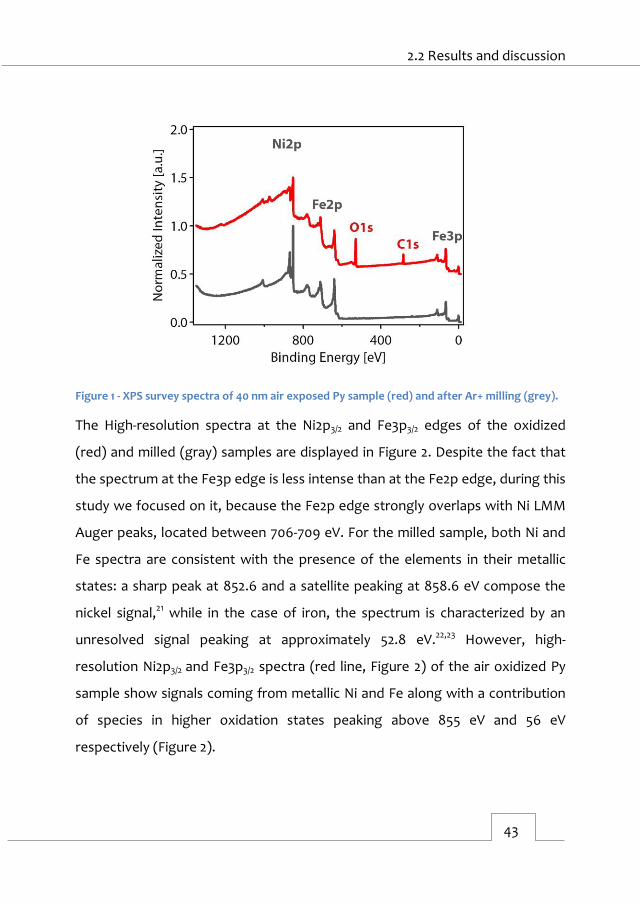
2.2 Results and discussion
43
Figure 1 - XPS survey spectra of 40 nm air exposed Py sample (red) and after Ar+ milling (grey).
The High-resolution spectra at the Ni2p3/2 and Fe3p3/2 edges of the oxidized
(red) and milled (gray) samples are displayed in Figure 2. Despite the fact that
the spectrum at the Fe3p edge is less intense than at the Fe2p edge, during this
study we focused on it, because the Fe2p edge strongly overlaps with Ni LMM
Auger peaks, located between 706-709 eV. For the milled sample, both Ni and
Fe spectra are consistent with the presence of the elements in their metallic
states: a sharp peak at 852.6 and a satellite peaking at 858.6 eV compose the
nickel signal,21 while in the case of iron, the spectrum is characterized by an
unresolved signal peaking at approximately 52.8 eV.22,23 However, high-
resolution Ni2p3/2 and Fe3p3/2 spectra (red line, Figure 2) of the air oxidized Py
sample show signals coming from metallic Ni and Fe along with a contribution
of species in higher oxidation states peaking above 855 eV and 56 eV
respectively (Figure 2).

2 Self-assembled monolayers on Permalloy
44
Figure 2 - High-resolution XPS spectra at the Ni2p3/2 (a) and Fe3p3/2 (b) edges of Py films subjected to different treatments: Ar+ milling (reference, gray), air oxidation (no plasma, red), H2 plasma (black), O2 plasma (blue).
Next, we studied the effect of hydrogen and oxygen plasma treatments on
our Py films. These kind of treatments have been commonly used on other
oxides like alumina, with the twofold aim of cleaning the surface and increasing
the density of binding sites thus promoting SAM formation.24 XPS
measurements revealed that the surface composition of O2 and H2 plasma–
treated samples is significantly affected by this process. These changes are
appreciable in the Ni2p3/2 and Fe3p3/2 spectra (Figure 2, black and blue lines) and
especially in the O1s high-resolution XPS spectrum (Figure 3).

2.2 Results and discussion
45
Figure 3 - Top: Deconvoluted high-resolution O1s XPS spectrum of an air oxidized Py film (red line) without any additional plasma treatment. Bottom: The upper spectrum is compared with those of Py films subjected to H2 (black) and O2 (blue) plasmas.
The top part of Figure 3 shows the O1s high-resolution XPS spectra of an air
oxidized (no plasma) sample. In agreement with previous reports, the total
spectrum results from the contribution of different oxygen species present in
the sample: bulk (O2-, 529.6 eV), hydroxyl (OH-, 531.2 eV) and weakly bound
oxygen species and contamination (532.9 eV).25,22,26
After the hydrogen plasma treatment, changes in the shape of the O1s
spectrum are evident, with an increase of the signal coming from hydroxyl
groups at the expense of that of bulk oxygen. This is consistent with the
transformation of some metal oxide into hydroxide species. This marked

2 Self-assembled monolayers on Permalloy
46
increase of the hydroxyl peak has not been observed in the case of the oxygen
plasma treated sample. Nevertheless, in this later case, an overall increase in
the O1s signal with respect to the non-treated sample is detected. These
changes are accompanied by the disappearance of the metallic iron and nickel
contributions in the Ni2p and Fe3p spectra (Figure 2, blue line) and point to the
formation of a thicker Py oxide as a result of the oxygen plasma treatment.
We performed XRR measurements to evaluate the oxide thickness after the
plasma treatments. The collected reflectivity curves are shown in Figure 4a; the
model used to fit the curves is represented in Figure 4b. We fitted the data to a
three-slab structure to obtain the density (ρ) and the thickness (T) of the Py
and the Py oxide (PyOx) layers.
Figure 4 – a) XRR reflectograms of Py surface subjected to different treatments: bare sample (red dots), H2 plasma (black dots) and O2 plasma (blue dots). b) Model used to fit the curves.
The obtained results are listed in Table 1. These values seem to confirm the
increase in the oxide thickness after the O2 plasma treatment, while in the H2
plasma treated sample no effective change is appreciable.

2.2 Results and discussion
47
Table 1 – Parameters obtained from the fittings of XRR data of Py samples subjected to different treatments: ρ is the density and T is the thickness of each layer.
Sample ρPyOx [g/cm3] TPyOx [nm] ρPy [g/cm3] TPy [nm]
Bare 6.85 1.8 8.6 8.2
H2 Plasma 6.74 1.7 8.6 8.3
O2 Plasma 7.61 2.9 8.6 7.1
Figure 5 - AFM topographic images (1x1 µm2) of Py substrates after different plasma treatments: a) air oxidized Py substrate, b) Weak H2 Plasma, c) Strong H2 Plasma, d) Weak O2 Plasma, e) Strong O2 Plasma.
Finally, we checked by AFM, the morphology of the treated samples (Figure 5).
In spite of the difference in composition, plasma treatments do not lead the
appreciable changes in the morphology of the surface with root mean square
(RMS) roughness values around 0.16 nm, comparable to that of the air oxidized
sample.
2.2.1 Preparation of SAMs
In the second part of our study we investigated how APAs of different carbon
chain lengths (CH3(CH2)n-1PO3H = CnP; n being number of C atoms) are anchored
on Py substrates. We have used wθCA measurements to evaluate the extent
and quality of the formed SAMs. Due to the hydrophobic character of alkyl
chains used in this study, an increase in wθCA can be directly related with an

2 Self-assembled monolayers on Permalloy
48
improvement of the quality of the SAM. During control experiments, we used
Py samples exposed to the same surface pre-treatments but dipped in neat
solvent as references. According to the literature, the best reported conditions
to form good quality APAs SAMs over metal oxide surface were the use of 2
mM APA 2-propanol solutions.27,28 In table 2 the wθCA values obtained using that
functionalization conditions for the each different pretreatment are reported.
Table 2 - wθCA values for samples subjected to different treatments and functionalized with different APAs. Ø is the neat solvent.
Sample wθAA [º] wθRA [º] Sample wθAA [º] wθRA [º] Sample wθAA [º] wθRA [º] Bare 40 12 H2 Plasma 22 10 O2 Plasma 18 10
Ø 45 15 H2-Ø 48 19 O2-Ø 40 12
C12P 90 77 H2-C12P 107 80 O2-C12P 44 17
C14P 94 80 H2-C14P 109 87 O2-C14P 46 19
C16P 98 85 H2-C16P 112 92 O2-C16P 52 20
C18P 100 87 H2-C18P 116 95 O2-C18P 50 21
As can be seen, the wθCA values of APA functionalized samples are always
higher than those for the corresponding reference samples. In particular, wθCA
values of the SAMs formed on H2 plasma treated Py samples are higher than
those measured for SAMs on O2 or air oxidized samples. Moreover, they are
comparable with those obtained by Allara et al.,29 or Pellerite et al.30 on alumina
oxide or Spori et al. on titanium oxide.31 We also observed that the
functionalized substrates exhibit low hysteresis of the contact angle, from 27º
for C12P to 21º for of C18P, which reflects the good quality of the formed SAMs.
We attribute this behavior to the fact that, according to XPS, H2 plasma
promotes the formation of metal hydroxides that probably favors the
formation of surface bound phosphoric esters during the grafting process.32,33

2.2 Results and discussion
49
Therefore, H2 plasma treated samples will be used through the rest of the
chapter.
Kinetics studies. We studied the kinetics of the self-assembly process at room
temperature for the C12P and C18P SAMs, and modeled the evolution of the
wθCA as function of time. We prepared a set of samples treated with H2 plasma
and immersed them in an APA solution for reaction times ranging from 1
second up to 16 hours.
Cassie’s Law34 states that the θCA of a liquid on a composite surface can be
obtained from the area fraction and the contact angles of each component,
cos 𝜃𝐶𝐴 = 𝑓1 cos𝑤𝜃1 + 𝑓2 cos𝑤𝜃2 [Eq.1]
where wθ1 is the contact angle and f1 is the area fraction for component 1 and
wθ2 is the contact angle and f2 is the area fraction for component 2. Accepting
that the Py-APA system follows Cassie’s law, we can consider that Py is
component one and APA SAM is component 2.34 Taking into account that wPy
= 30º and cos wPy ≈ 1, the surface coverage, - defined as the number of
adsorbed molecules on a surface divided by the number of molecules in a filled
monolayer on that surface - can be estimated at a given functionalization time
as:
Γ =1 − cos𝑤𝜃𝑡1 − cos𝑤𝜃∞
[Eq.2]

2 Self-assembled monolayers on Permalloy
50
where wt is the measured contact angle at time t and w is the measured
contact angle for a fully functionalized surface. The measured coverage values
as function of time are represented in Figure 6.
Figure 6 - Coverage as a function of time for a Py substrate functionalized with 2 mM C12P (solid circle) and C18P (hollow circle) 2-propanol solutions. Data have been fitted to a biexponential Langmuir isotherm (dashed red line).
As can be seen, no significant differences in coverage as a function of time are
detected between C12P and C18P. First, we tried to model the data using a
Langmuir isotherm with a single rate constant:
Γ = 1 – e-kCt [Eq.3]
In this equation, again is the surface coverage, k is the kinetic absorption
constant, C is the concentration of the APA and t is the dipping time. However,

2.2 Results and discussion
51
we were unable to describe our data with Eq.3. This simple model considers
irreversible binding to the surface, only takes into account the number of the
available sites on the surface and that the molecules adsorb into an immobile
state without interactions with adjacent sites. As a result, it has shown to be
insufficient to described the behavior observed in Figure 6.35 To be able to build
an effective adsorption model for our system, we were forced to consider a
biexponential function (Eq. 4 and dashed line in Figure 6), that describes the
formation of the monolayer as two cooperative processes:36,37
Γ = 1 − 𝑎𝑒−𝑘1𝐶𝑡 − (1 − 𝑎)𝑒−𝑘2𝐶𝑡 [Eq.4]
The difference of several orders of magnitude in the two k values obtained
after the fitting (k1 = 1400 M-1s-1 and k2 = 0.4 M-1s-1) can be rationalized as follows:
Initial growth (k1) is fast due to high availability of reaction sites. However, as
time goes by, further growth is quenched. The slowing of the process may be
caused by several factors, for example the hindering of reaction sites by the
molecules that are already grafted, or the presence of physisorbed solvent
molecules. The diffusion of the incoming molecules involves a rearrangement
of the molecules, and the approaching of the entering surfactant molecules
requires higher activation energy; all this is reflected in the smaller value of the
second-rate constant.

2 Self-assembled monolayers on Permalloy
52
Figure 7 - SAM growth models: a) Uniform growth model: a complete monolayer is formed and the thickness increases synchronously as a function of time (i-ii). b) Island-like growth model: the molecules arrange themselves into discrete domains: (i) when two domains come in contact, coalescence takes place forming a bigger domain, which continues to grow until a complete monolayer is formed (ii). The thickness is maintained through the self-assembly.
Growth mechanism. Two main growth models have been reported for SAMs, as
represented in Figure 7, namely the uniform growth (Figure 7a) and the island-
like growth (Figure 7b). In the first one, a liquid-like, disordered film with
molecules lying flat to the surface is formed all over the surface (SAM thickness
at a given time is lower than the final thickness T’<<T, figure 7a,i); as the
grafting process goes on and the coverage increases, more molecules are
incorporated to the assembly, which is eventually converted into the final,
highly ordered film structure, with the expected final SAM thickness (T, Figure
7a,ii). In contrast, for the second model, islands of densely packed molecules
with a local structure similar to the complete monolayers are formed from the
beginning of the assembly process (Figure 7b,i). When coverage increases,

2.2 Results and discussion
53
these islands grow laterally and when they enter in contact with another one,
they join to form larger aggregates (coalescence process), (Figure 7b,ii). This
process continues until a complete monolayer is formed. For example,
Woodward et al. performed AFM measurements on quenched mica substrates
functionalized with APAs during the SAM growth, and demonstrated that the
formation proceeded by nucleation, growth and coalescence of submonolayer
islands.38 A similar behavior was observed by Gawalt et al. while functionalizing
titanium oxide.15 On the other hand, Helmy et al.36 studied the functionalization
of titanium oxide with APA by means of IRRAS, monitoring the position of the
methylene stretching and observed that in the early stage of the reaction,
molecules were randomly distributed on the surface, while as the coverage
increased, the order in the monolayer gradually increased until reaching the
final highly ordered state.
In order to investigate if the growing mechanism of APAs on Py fits into one of
the above cases, we imaged samples treated with 2 mM C18P 2-propanol
solutions for short periods of time (less than 1 minute, or 85% coverage
according to Figure 6) using AFM. This is represented in Figure 8.

2 Self-assembled monolayers on Permalloy
54
Figure 8 – (a-f) AFM images of a functionalized Py substrate with C18P took at different times.
Samples did not show evidence of island-like features. Instead, homogenous
surfaces were imaged suggesting the presence of surfactant molecules
randomly distributed on the surface according to a uniform growth
mechanism.39,40
2.2.2 Structural Characterization
Once the optimum conditions for APA SAMs growth on Py were settled, and
the mechanism and kinetics of the process clarified, we continued with their
structural characterization. For that purpose, we used several surface based
characterization techniques to shine light on their internal structure.

2.2 Results and discussion
55
AFM imaging. Tapping mode AFM topography images of 15 nm H2 plasma
treated Py samples immersed for 16h in neat solvents or in solutions of APA
with different chain lengths, were routinely performed and are shown in Figure
9. Noticeably, the growing process took part without a substantial increase in
surface roughness. The RMS values measured using AFM for fully covered
samples (approx. 0.28 nm) were slightly above to that of a Py substrate
immersed in neat solvent during the same amount of time (RMS ≈ 0.18 nm).
Figure 9 - AFM topographic images (1x1 µm2) of H2 plasma treated Py substrates: a) neat solvent, b) C12P SAM, c) C14P SAM, d) C16P SAM, e) C18P SAM.
Mass spectrometry. CnP (n=12, 14, 16, 18) SAMs on 15 nm Py were analyzed by
MALDI-TOF spectrometry (Figure 10) in order to prove the presence and
integrity of the molecule on the Py substrate. Last developments in
instrumentation have permitted to apply this technique to the detection of thin
films and SAMs and even to differentiate between monolayer and multilayer
formation on surfaces.41 For n= 12-16, peaks corresponding to the [CnPH]+
molecular ions were visible at the right mass-to-charge ratio. In the case of the
C18P monolayer, this species cannot be clearly identified without ambiguity as a
result of interfering peaks coming from the polymer matrix used during the
experiments. Quiñones et al., functionalized nickel oxide with APA, and
characterized the resulting SAMs using MALDI-TOF.20 They observed the

2 Self-assembled monolayers on Permalloy
56
presence of signals arising from dimer plus one hydrogen (m/z=672, for C18P
dimer) formed during the assembly process. They correlated this signal with
the presence of multilayers in their films.20,41 In our case, we did not observe
peaks correlated to dimers, but exclusively peaks associated with the molecular
ion. This suggests that single layer APA films are formed over Py, as will be later
confirmed using XRR.
Figure 10 - MALDI-TOF spectra measured for C12P (Mw=250.31), C14P (Mw=278.37) and C16P (Mw=306.42) SAM-functionalized Py substrates.
Infrared spectroscopy. Next, we used IRRAS to further confirm the presence
of the molecules on the surface and to estimate the degree of order and the tilt
of the alkyl chains in the SAMs.
Figure 11 shows the C-H stretching region of the corresponding spectra for the
two extremes of alkylphosphonate SAMs used in this work: C12P (red line) and

2.2 Results and discussion
57
C18P (black line). Four peaks are identified in the spectra of APA SAMs on Py,
which can be assigned from left to right to the CH3as (~2965 cm-1), CH2as (~2924
cm-1), CH3sy (~2879 cm-1) and CH2sy (~2854 cm-1) vibrations. Nevertheless, in
some cases the CH3sy peak was not observed due to its low intensity and
intrinsic noise in the measurements. It is well known that the position of the
methylene peaks gives information about the degree of order in the molecular
layer: the higher the energy, the lower the order.42 As shown in Figure 11,
methylene asymmetric and symmetric peaks show a gradual red shift when
going from C12P (2927 and 2856 cm-1) to C18P SAM (2923 and 2852 cm-1) with
intermediate values for alkyl chains of intermediate length (Figure 12a).30,43
These values indicate an evolution from a more liquid-like assembly in the
shorter chains to a more crystalline structure in the longer chains, even though
values are slightly above those reported for fully crystalline state (<2920 and
2850 cm-1).

2 Self-assembled monolayers on Permalloy
58
Figure 11 - IRRAS spectra of the region corresponding to the alkyl C-H stretching. C12P (red) and C18P (black) SAM-functionalized substrates. Vertical gray lines are a reference for the eye and mark the position of C18P methylene vibrations.
Additional information about the tilt angle () of the alkyl chain with respect to
the surface normal was obtained from the peak intensity ratios of the
methylene and methyl asymmetric stretches.44 As described by Greenler in
reference 44, the relation between and the relative intensities of the CH2as
and CH3as peaks is given by:43,14
I(CH2)/I(CH3) = (2/3)·m·[cos2(90-α)/ cos2(35- α)] [Eq.5]
where I is the peak intensity, m is the number of methylene units in the chain
and is the tilt angle in degrees. The angles 90º and 35º are geometrical
constants derived from the direction of the relevant stretches with respect to
the long molecular axis.

2.2 Results and discussion
59
Table 3 - Tilt angles [º] and thicknesses [Å] of different APA SAMs on Py estimated from the IRRAS spectra.
Number of C Tilt angle [º] IR Thickness [Å]
18 23 22
16 24 19
14 27 16
12 31 14
Figure 12 - Data analysis of the IRRAS measurements: (a) Position of the C-H bond antisymmetric strecth for alkylphosphonic acids of different chain length. (b) Estimated chain tilt angle (α) with respect to the surface normal of alkyl phosphonic acids of different chain length. (c) Estimated thicknesses from IRRAS spectra of monolayers with different chain length (black dots) and calculated thicknesses for vertical aligned all trans configuration (gray dots).

2 Self-assembled monolayers on Permalloy
60
As summarized in table 3 and Figure 12b, the tilt angles progressively change
from 31º (C12P) to 23º (C18P) when the chain length increases, in good
agreement with previous observations. For example, Spori et al. reported a
change in tilt angle of APA SAMs on titania from approximately 45º to 30 º
when increasing the phosphonic chain length from twelve to eighteen
carbons31 and Levine et al. on alumina from 33 º to 26 º when going from eight
to sixteen carbons.45
The theoretical thickness of a perfectly stretched (all-trans) APA SAM as
function of the tilt angle (assuming a tridentate binding to the surface), bond
angles of 109.5° and bond-lengths of 1.78 Å C-P, 1.55 Å P-O, 1.54 Å C-C (Figure 13),
can be described according to Eq. 6 :
T[Å] = 2.30 + ((n/2)-1)·2.51·cos() + 1.54·cos (35.25) [Eq.6]
being n the number of C atoms in the chain and α the tilt angle. From the tilt
angles obtained from the IR analysis (Table 3 and eq. 6) we can estimate SAM
thicknesses for different chain lengths (Table 3 and Figure 12c). One can see
that the difference between the experimental and the theoretical thickness of
the formed SAMs is roughly of 2 nm, which is in good agreement with the
observed tilt angles.

2.2 Results and discussion
61
Figure 13 - Sketch of an alkylphosphonic acid anchored to the surface through a tridentate binding. Angles and bond distances used to estimate the theoretical thickness of a SAM are included.
Figure 14 - a) XRR reflectograms of Py surface subjected to H2 plasma (black dots) and then functionalized with CnP : C12P (pink dots), C14P (orange dots), C16P (green dots) and C18P (purple dots). b) Model used to fit the curves (solid lines in (a)).

2 Self-assembled monolayers on Permalloy
62
X-Ray Reflectivity. XRR was used to confirm the calculated film thicknesses and
estimate SAM densities (ρ). XRR spectra of the functionalized CnP Py samples,
are showed in Figure 14a. The reflectograms have been modeled using a three-
slab model (SAM/Oxide/Metal) displayed in Figure 14b, where the monolayers
density (ρ) is kept constant throughout all the film.
As observed in figure 14, when going from shorter to longer chain lengths the
film thickness increases (the thicker film, the shorter period of the oscillations)
The measured average film density is ρav ≈ 0.78 g/cm3 and the thicknesses (T)
are those reported in Table 4. For the calculation, we fixed the PyOx and Py
densities to 8.6 g/cm3, according to the values reported in Table 1.
Table 4 - Densities and thickness obtained from the fitting of data represented in Figure 13 to a the three slab model. * indicates which parameters were fixed during the fitting.
Sample ρCnP
[g/cm3]
TCnP
[nm]
ρPyOx
[g/cm3]*
TPyOx
[nm]*
ρPy
[g/cm3]*
TPy
[nm]
Bare - - 6.74 1.7 8.6 13.3
C12P 0.78 1.5 6.74 1.7 8.6 11.8
C14P 0.78 1.7 6.74 1.7 8.6 11.6
C16P 0.78 2.0 6.74 1.7 8.6 11.3
C18P 0.78 2.5 6.74 1.7 8.6 10.8
Considering the films formed by a P atom and an alkyl chain, the area per
molecule (ApM = Mw/(ρav·T·NA)·1024 can be estimated to be 24.5 Å2 for a C18P

2.2 Results and discussion
63
film (Mw = 284.46 and Z = 160) and 26.5 Å2 (Mw = 230.30 and Z = 112) for a C12P
film. These values are not very far from those reported for other model
systems: alkylsiloxanes on silicon (21 Å2),39 thiols on gold (21.7 Å2),46 or
alkylphosphonic acids on alumina (28-57 Å2) this results further supports the
good quality of the assembled films.45
XPS measurements. High resolution P2p XPS spectrum of a C18P functionalized
Py sample, shows the presence of phosphorous (Figure 15), confirming the
successful grafting of the molecules on the surface. Moreover, the adsorption
of SAMs of increasing chain lengths resulted in a progressive attenuation of the
different substrate core level signals.

2 Self-assembled monolayers on Permalloy
64
Figure 15 - P2p3/2 XPS spectra of: (a) bare Py substrate. (b) C18P SAM on Py.
The thickness increase with the respect of C12P (T-T12), can be estimated using
the following formula:47
(T-T12) = cos ln (In / I12) [Eq.7]
where I is the intensity of the measured signal, T the thickness of the film, T12
the thickness of the C12P SAM, n refers to the number of carbon atoms in a

2.2 Results and discussion
65
given measured alkyl chain, is the angle between the X-Ray source and the
sample and the attenuation length of the photoelectrons through the
hydrocarbon layer.
We used the intensity values of the Ni2p signal to obtain the thickness increase
per methylene group (d) for each of the studied APA, Figure 16 a. The value of
was set to 35.4 Å as estimated using the empirical equation reported by Bain
and Whitesides.48
Figure 16 - Relative thickness of APA monolayers formed on Py as determined from XPS, XRR and IRRAS.
Figure 16 compares the thickness increase as function of the number of
carbons estimated using XPS, XRR (Table 4) and IRRAS (Table 3) data. From this
data, the d can be calculated from a linear fit of the measured relative
thicknesses with respect to the number of carbons in the alkyl chain. The XPS

2 Self-assembled monolayers on Permalloy
66
value 1.44 Å/CH2, is in agreement with the d values reported in Table 3 and
Table4 and calculated from XRR (1.48 Å/CH2, Figure 16b) and IRRAS
measurements (1.32 Å/CH2, Figure 16c). All those values are higher than 1.26
Å/CH2, the value expected for a perpendicular fully extended alkyl chain with C-
C distances equal to 1.54 Å. This fact reflects the progressive reduction of the
monolayer tilt angles when going towards longer chain lengths.
2.2.3 Magnetic characterization of modified substrates
One of the most valuable properties of Py is its FM behavior at room
temperature. This is the reason why the study of its magnetism before and
after the SAM formation is important. In order to characterize the magnetic
properties of the Py films, we took advantage of magneto-optical Kerr effect
(MOKE) spectroscopy.49 This technique has a very high surface sensitivity and is
able to register hysteresis loops of a magnetic sample by measuring the
rotation in the polarization plane (Kerr rotation) of the light reflected on the
surface.
The Py oxide behaves at room temperature as a paramagnet and it does not
affect the magnetic behavior of the underlying Py film. Below 195 K, (Neel T)
the Py oxide undergoes a long-range AF ordering. This results in an exchange
bias interaction between the AF oxide and the FM Py layer, which induces an
enhancement of coercive field in the magnetic hysteresis loop.12,13,50
We prepared a set of Py samples subjected to different treatments, as
represented in Figure 17: an O2 and H2 plasma-treated samples (red and blue), a
H2 plasma-treated sample that was then functionalized with an APA SAM

2.2 Results and discussion
67
(green), an air-oxidized sample without any further treatment (gray) and a
gold-capped Py sample that was used as a reference (black).
Figure 17 - Preparation of the different samples used for the MOKE measurements.
In Figure 18 the hysteresis curves recorded using MOKE at 22 K (top) after field
cool at 325 mT and at room temperature (bottom) are shown.

2 Self-assembled monolayers on Permalloy
68
Figure 18 - Low temperature (top) vs room temperature (bottom) magnetization (measured using MOKE technique) recorded for a non-oxidized gold-capped Py sample (Capped) and air oxidized (Bare), pre-treated with hydrogen plasma (H2), pre-treated with hydrogen plasma and APA functionalized (SAM) and pre-treated with oxygen plasma (O2) samples.
All the samples show a similar coercive field of about 9 mT at room
temperature (Figure 18). In contrast, well below the Neél temperature of the
AF oxide, the samples show an increase in coercivity. The coercive field values
are 50 mT for the oxygen treated sample, ca. 13 mT for the hydrogen treated
samples and 14 mT for the air oxidized sample. No appreciable increase in
coercivity has been observed for the gold protected sample (9 mT). The
magnitude of the effect is larger for the oxygen, in accordance with the
presence of a thicker oxide layer in this sample (Table 1). This result points out

2.2 Results and discussion
69
that the SAM formation process preserves the integrity of the native oxide
layer and that the magnetic properties of the Py film are unaltered after the
grafting process.
2.2.4 APA SAMs Applications
As resist agents. The fabrication of microstructures using patterned SAMs as
nanometric etch-resistant masks has been used successfully in nanoelectronics
and nanofabrication. SAMs can be locally formed by means of microcontact
printing lithography (µCP). This soft lithography uses the relief patterns on a
master stamp to transcribe patterns of an ink (e.g. a SAM) through conformal
contact on the surface of a substrate. As pointed out above, each kind of
substrate needs a specific derivatized molecule. Thus, alkanethiols have been
commonly used on metals, while acid-functionalized molecules as carboxylic or
phosphonic acids have been chosen for metal oxides like aluminum and glass.
However, patterned SAMs on Py have never been fabricated51 despite the fact
that, arrays and films of different shapes and structures of Py have been
intensively studied during the last years, due to their interest in
nanomagnetism52 and in storage technologies.53 In this scenario, we tested APA
SAMs on Py as potential resists to fabricate nanostructured substrates.
In order to prepare the polymeric stamp, we used a compact disc (CD) as mold
due to its periodic pattern of stripes. After removing the protective coating of
the CD, a polydimethylsiloxane (PDMS) solution was spin-coated on it and
annealed in air atmosphere. The PDMS stamp was then piled off, and after
being soaked with a fresh APA solution, it was used to transfer SAMs patterns

2 Self-assembled monolayers on Permalloy
70
onto hydrogen activated Py surfaces. Although, the APA isopropanolic solution,
used for the preparation of SAMs by immersion method, gave rise to non-
homogeneous SAM deposition, when we substituted isopropanol as ink media
with diethylene glycol (a solvent of higher density and lower vapor pressure
ending), well defined and compact SAM patterns were obtained. We used
contact mode AFM to obtain the friction image (Figure 19a), because the
nanometric thick features were not distinguishable from the non-patterned
regions. After performing an etching of the Py with glycolic acid (GA), bare Py
regions were attacked while the APA SAM protected regions remained intact.
The high control of the spreading effect during SAM formation is highlighted by
the sub-micrometric size of the developed structures (Figure 19b and 19c).

2.2 Results and discussion
71
Figure 19 - a) Friction AFM image of 15 µm2 of C18P SAM stripes patterned on a ~16 nm thick Py substrate, taken before etching. b) Topographic AFM image of sample showed in (a) after the etching treatment. c) Height profile corresponding from the blue line in (a) and the red line in (b).
As layer by layer templates. Later on, our group reported the use of the
methodologies described in this chapter to template the layer-by-layer (LbL)
growth of NASF-1 films, a surface metal organic framework (surMOF) on Py
films.54 By directing MOF transfer with APA SAMs, very smooth, homogeneous,
highly oriented and ultrathin films across millimeter-scale areas were achieved
that display moderate conductivity likely due to electron hopping. Here, the
SAM was key for directing the transfer.

2 Self-assembled monolayers on Permalloy
72
2.3 Conclusions
The successful and optimized formation of SAMs based on APAs has been
accomplished on oxidized Py surfaces for the first time. It has been
demonstrated that a crucial and critical point is the use of hydrogen plasma as
pre-treatment. This plasma, instead of acting as a reducing agent for the oxide,
promoted the formation of metal hydroxides, as analyzed by XPS, that assist
the binding of the phosphonic acid groups during the grafting process and
determines the successful formation of high quality SAMs.
Detailed structural characterization of the monolayers has been performed by
means of different techniques. According to wCA, XPS, MALDI-TOF and XRR,
the APA SAMs formed on Py are comparable to other well-studied systems in
terms of quality. Additional magneto-optical measurements have been carried
out to discard any possible modification of the magnetic behavior of the Py film
during the SAM growth, which would rule out its later application.
The use of microcontact printing, a soft lithographic technique, has allowed the
formation of well-defined SAM patterns on Py. The quality of this printed SAM
guarantees its use as protecting layer when exposing Py to an etching agent,
giving rise to a wet chemical approach for line-of-sight patterning of Py
surfaces. This result is very relevant for the interest of these hybrid interfaces in
nanomagnetism and their potential applications like circuitry or storage
technologies.

2.3 Conclusions
73
This work extends the already large number of utilities of Py, with the
controllable modification of its surface by well-organized, strongly attached
molecular units. We have also demonstrated that by directing MOF transfer
with APA SAMs, very smooth, homogeneous, highly oriented and ultrathin
surMOF films on ferromagnetic surfaces can be obtained.
.
2 Self-assembled monolayers on Permalloy
74
2.4. References
1. Nahrwold, G. et al. Structural, magnetic, and transport properties of
Permalloy for spintronic experiments. J. Appl. Phys. 108, 13907 (2010).
2. Davis, J. R. Nickel, cobalt, and their alloys. (ASM international, 2000).
3. Rao, S. S. et al. Positive exchange bias in epitaxial permalloy/MgO
integrated with Si (100). Curr. Opin. Solid State Mater. Sci. 18, 140–146
(2014).
4. Ishihara, Y., Itou, N., Kimijima, T. & Hirano, T. Clean aluminum oxide
formation on surface of aluminum cylinder in an ultraclean gas-sampling
system. J. Vac. Sci. Technol. A Vacuum, Surfaces, Film. 17, 3139–3143
(1999).
5. Smardz, L., Köbler, U. & Zinn, W. Oxidation kinetics of thin and ultrathin
cobalt films. J. Appl. Phys. 71, 5199–5204 (1992).
6. Li, J., Mayer, J. W. & Colgan, E. G. Oxidation and protection in copper
and copper alloy thin films. J. Appl. Phys. 70, 2820–2827 (1991).
7. Lee, W.-Y. Oxidation Studies of Permalloy Films by Quartz Crystal
Microbalance, AES, and XPS. J. Electrochem. Soc. 124, 1747–1751 (1977).
8. Fitzsimmons, M. R., Silva, T. J. & Crawford, T. M. Surface oxidation of
Permalloy thin films. Phys. Rev. B 73, 14420 (2006).
9. Brückner, W. et al. Oxidation of NiFe(20 wt.%) thin films. Mater. Sci. Eng.
B 86, 272–275 (2001).

75
10. Dagan, G. Passivation of Permalloy Thin Films. J. Electrochem. Soc. 139,
1855–1861 (1992).
11. Hsiao, R. & Mauri, D. Plasma-induced surface segregation and oxidation
in nickel-iron thin films. Appl. Surf. Sci. 157, 185–190 (2000).
12. Hagedorn, F. B. Exchange anisotropy in oxidized permalloy thin films at
low temperatures. J. Appl. Phys. 38, 3641–3645 (1967).
13. Hagedorn, F. B. Anomalous Hysteresis Loops in Permalloy Thin Films
near 4.2°K. J. Appl. Phys. 38, 1362–1363 (1967).
14. Thissen, P., Valtiner, M. & Grundmeier, G. Stability of Phosphonic Acid
Self-Assembled Monolayers on Amorphous and Single-Crystalline
Aluminum Oxide Surfaces in Aqueous Solution. Langmuir 26, 156–164
(2010).
15. Gawalt, E. S., Avaltroni, M. J., Koch, N. & Schwartz, J. Self-Assembly and
Bonding of Alkanephosphonic Acids on the Native Oxide Surface of
Titanium. Langmuir 17, 5736–5738 (2001).
16. Raman, A. et al. Understanding Organic Film Behavior on Alloy and Metal
Oxides. Langmuir 26, 1747–1754 (2010).
17. Gao, W., Dickinson, L., Grozinger, C., Morin, F. G. & Reven, L. Self-
Assembled Monolayers of Alkylphosphonic Acids on Metal Oxides.
Langmuir 12, 6429–6435 (1996).
18. Badia, A., Lennox, R. B. & Reven, L. A Dynamic View of Self-Assembled

2 Self-assembled monolayers on Permalloy
76
Monolayers. Acc. Chem. Res. 33, 475–481 (2000).
19. Zschieschang, U., Halik, M. & Klauk, H. Microcontact-Printed Self-
Assembled Monolayers as Ultrathin Gate Dielectrics in Organic Thin-Film
Transistors and Complementary Circuits. Langmuir 24, 1665–1669 (2008).
20. Quiñones, R., Raman, A. & Gawalt, E. S. Functionalization of nickel oxide
using alkylphosphonic acid self-assembled monolayers. Thin Solid Films
516, 8774–8781 (2008).
21. Grosvenor, A. P., Biesinger, M. C., Smart, R. S. C. & McIntyre, N. S. New
interpretations of XPS spectra of nickel metal and oxides. Surf. Sci. 600,
1771–1779 (2006).
22. Pollak, R. A. & Bajorek, C. H. Surface composition and chemistry of
evaporated Permalloy films observed by x−ray photoemission
spectroscopy and by Auger electron spectroscopy. J. Appl. Phys. 46,
1382–1388 (1975).
23. McIntyre, N. S. & Zetaruk, D. G. X-ray photoelectron spectroscopic
studies of iron oxides. Anal Chem 49, 1521–1529 (1977).
24. Otto, C. et al. Physical Methods for Cleaning and Disinfection of
Surfaces. Food Eng. Rev. 3, 171–188 (2011).
25. Rajalingam, S., Devillers, S., Dehalle, J. & Mekhalif, Z. A two step process
to form organothiol self-assembled monolayers on nickel surfaces. Thin
Solid Films 522, 247–253 (2012).

77
26. Lee, W. Effects of Oxidation on the Atmospheric Corrosion of Permalloy
Films. J. Electrochem. Soc. 126, 1533–1539 (1979).
27. Hannon, J. B., Afzali, A., Klinke, C. & Avouris, P. Selective placement of
carbon nanotubes on metal-oxide surfaces. Langmuir 21, 8569–8571
(2005).
28. Zschieschang, U. et al. Mixed Self-Assembled Monolayer Gate Dielectrics
for Continuous Threshold Voltage Control in Organic Transistors and
Circuits. Adv. Mater. 22, 4489–4493 (2010).
29. Allara, D. L. & Nuzzo, R. G. Spontaneously organized molecular
assemblies. 1. Formation, dynamics, and physical properties of n-alkanoic
acids adsorbed from solution on an oxidized aluminum surface.
Langmuir 1, 45–52 (1985).
30. Pellerite, M. J., Dunbar, T. D., Boardman, L. D. & Wood, E. J. Effects of
Fluorination on Self-Assembled Monolayer Formation from
Alkanephosphonic Acids on Aluminum: Kinetics and Structure. J. Phys.
Chem. B 107, 11726–11736 (2003).
31. Spori, D. M. et al. Influence of Alkyl Chain Length on Phosphate Self-
Assembled Monolayers. Langmuir 23, 8053–8060 (2007).
32. Giza, M., Thissen, P. & Grundmeier, G. Adsorption Kinetics of
Organophosphonic Acids on Plasma-Modified Oxide-Covered Aluminum
Surfaces. Langmuir 24, 8688–8694 (2008).
33. Chockalingam, M., Darwish, N., Le Saux, G. & Gooding, J. J. Importance

2 Self-assembled monolayers on Permalloy
78
of the Indium Tin Oxide Substrate on the Quality of Self-Assembled
Monolayers Formed from Organophosphonic Acids. Langmuir 27, 2545–
2552 (2011).
34. Cassie, A. B. D. & Baxter, S. Wettability of porous surfaces. Trans.
Faraday Soc. 40, 546 (1944).
35. Schreiber, F. Structure and growth of self-assembling monolayers. Prog.
Surf. Sci. 65, 151–256 (2000).
36. Helmy, R. & Fadeev, A. Y. Self-Assembled Monolayers Supported on
TiO2: Comparison of C18H37SiX3 (X = H, Cl, OCH3), C18H37Si(CH3)2Cl, and
C18H37PO(OH)2. Langmuir 18, 8924–8928 (2002).
37. Major, R. C. & Zhu, X. Y. Two-Step Approach to the Formation of Organic
Monolayers on the Silicon Oxide Surface. Langmuir 17, 5576–5580 (2001).
38. Woodward, J. T. & Schwartz, D. K. In Situ Observation of Self-Assembled
Monolayer Growth. J. Am. Chem. Soc. 118, 7861–7862 (1996).
39. Wasserman, S. R. et al. The structure of self-assembled monolayers of
alkylsiloxanes on silicon: a comparison of results from ellipsometry and
low-angle x-ray reflectivity. J. Am. Chem. Soc. 111, 5852–5861 (1989).
40. Carraro, C., Yauw, O. W., Sung, M. M. & Maboudian, R. Observation of
Three Growth Mechanisms in Self-Assembled Monolayers. J. Phys. Chem.
B 102, 4441–4445 (1998).
41. Quiñones, R., Raman, A. & Gawalt, E. S. An approach to differentiating

79
between multi- and monolayers using MALDI-TOF MS. Surf. Interface
Anal. 39, 593–600 (2007).
42. Ulman, A. Formation and Structure of Self-Assembled Monolayers.
Chem. Rev. 96, 1533–1554 (1996).
43. Tillman, N., Ulman, A., Schildkraut, J. S. & Penner, T. L. Incorporation of
phenoxy groups in self-assembled monolayers of trichlorosilane
derivatives. Effects on film thickness, wettability, and molecular
orientation. J. Am. Chem. Soc. 110, 6136–6144 (1988).
44. Greenler, R. G. Infrared Study of Adsorbed Molecules on Metal Surfaces
by Reflection Techniques. J. Chem. Phys. 44, 310–315 (1966).
45. Levine, I. et al. Molecular Length, Monolayer Density, and Charge
Transport: Lessons from Al–AlOx/Alkyl–Phosphonate/Hg Junctions.
Langmuir 28, 404–415 (2012).
46. Dubois, L. Synthesis, Structure, and Properties of Model Oraganic
Surfaces. Annu. Rev. Phys. Chem. 43, 437–463 (1992).
47. Folkers, J. P. et al. Self-Assembled Monolayers of Long-Chain
Hydroxamic Acids on the Native Oxide of Metals. Langmuir 11, 813–824
(1995).
48. Bain, C. D. & Whitesides, G. M. Attenuation lengths of photoelectrons in
hydrocarbon films. J. Phys. Chem. 93, 1670–1673 (1989).
49. Rao, S. G. MOKE study of hybrid magnetic thin films: Permalloy on

2 Self-assembled monolayers on Permalloy
80
molecular self-assembled monolayer. Appl. Surf. Sci. 258, 5195–5199
(2012).
50. Nogués, J. et al. Exchange bias in nanostructures. Phys. Rep. 422, 65–117
(2005).
51. Burdinski, D., Saalmink, M., van den Berg, J. P. W. G. & van der Marel, C.
Universal Ink for Microcontact Printing. Angew. Chemie Int. Ed. 45, 4355–
4358 (2006).
52. Kohno, H. & Tatara, G. in Nanomagnetism and Spintronics 189–229
(Elsevier, 2009). doi:10.1016/B978-0-444-53114-8.00005-4
53. Mao, S. Tunneling magnetoresistive heads for magnetic data storage. J.
Nanosci. Nanotechnol. 7, 1–12 (2007).
54. Rubio-Giménez, V. et al. High-Quality Metal–Organic Framework
Ultrathin Films for Electronically Active Interfaces. J. Am. Chem. Soc. 138,
2576–2584 (2016).

81
3. Functionalization of
metallic ferromagnetic
surfaces
3.1. Introduction
In the previous chapter, we have used SAMs to functionalize passivated FM
surfaces. However, when a ferromagnet gets oxidized it can lose its surface
spin polarization properties and becomes useless as spin injecting electrode in
spintronic devices. Moreover, the oxide decouples the SAM and the FM metal
and prevents the use of SAM to tailor surface spin properties,1 and lowers the
device performance.2,3
Focusing on spintronic applications as one of the main goals of this thesis, in
this chapter we will go one step further and SAMs will be grafted directly on
FM metallic surfaces. In the literature, alkanethiols have been extensively used
to modify metallic surfaces like gold,4 but due to the difficulty to avoid their air
oxidation problems, the functionalization of metals like silver5 or copper6 is far
less extensive and there are only few works that face the direct assembly of
SAMs on FM metals like cobalt,7 iron8 or nickel9 and their alloys.
3
0

3 Functionalization of metallic ferromagnetic surfaces
82
Different strategies have been reported that describe the formation of SAMs
directly on bare FM metals. These methods could be divided in two groups: (i)
Strategies that avoid the formation of the oxide layer, and (ii) strategies that
recover the bare metal after removing the oxide layer.
(i) Strategies that avoid the formation of the oxide layer:
One of them is the use of vapor phase techniques to prevent the air exposure
of these materials. In this case, the FM material is prepared using ultra-high
vacuum techniques (UHV) (Figure 1a,i), then the molecule deposition is done
without exposing the sample to the air under reduced pressure (Figure 1a,ii) or
via vapor phase deposition under inert conditions. This limits the choice of
molecules to those having high vapor pressure. Notice that, if the UHV
chamber is directly connected to a glove box (inert atmosphere, Figure 1b,ii),
one can also form the SAM in solution. If the SAM does not protect the
substrate from reoxidation, the rest of layers and the top electrode must also
be deposited without breaking the inert atmosphere (Figure 1a-1b,iii) to form
the spintronic device. This approach have been used to functionalize a fresh
sputtered cobalt samples,10 which were transferred from the sputtering
system to a glove box, and then exposed to a dodecanethiol solution for 16
hours, after which SAM growth was observed.
A new approach recently reported to avoid the formation of native oxide is the
so-called template stripping (TS) method. It involves the evaporation under
UHV of a thin metal film on native silicon oxide surface or gold that is used as

3.1 Introduction
83
template. In the next step a rigid support, for example a glass substrate, is
glued against the metal so that a stack is formed by support/glue/metal. Next,
the support is stripped from the template giving a clean and oxide free metal
surface because up to this point, the bottom metal surface is in contact with
the template and protected from the ambient environment. This approach was
used by Kumar et al.11 to form an alkanethiol SAM on a nickel surface. They
evaporated a nickel film onto a perfluoroalkylsilane SAM modified silicon oxide
surface. This SAM was used in order to minimize the interaction between the
nickel and the bare silicon oxide surface, rendering easier the stripping process.
In order to avoid the nickel oxidation, TS was performed inside a glove box.
After this step, the TS nickel surface was exposed to a 3 mM ethanolic
alkanethiol solution and after 16 h the functionalization was completed. S2p
XPS analysis of the modified surface proved the presence of the metal-thiolate
bonds, without detecting any oxygen. The monolayer thickness and tilt angle
was also estimated, using angle resolved XPS, to be respectively 1.74 nm and
36º, which is in good agreement with previous reported results.8,9
(ii) Strategies that recover the bare metal after removing the oxide layer:
As an alternative strategy, the substrate once deposited is exposed to air and
its surface oxidizes. In order to functionalize the metallic surface, it is
mandatory to remove the oxide layer (Figure 1c,iiia), prior to the SAM
formation (Figure 1,iiic). Oxide removal is usually carried out in inert
atmosphere, using dry or wet etching methods.

3 Functionalization of metallic ferromagnetic surfaces
84
Figure 1 – Schematic representation of the fabrication of SAM-based spintronic devices. a) UHV route : i) bottom electrode deposition; ii) SAM formation; iii) top electrode deposition. b) UHV + GB route: i) bottom electrode deposition; ii) SAM formation in inert atmosphere; iii) top electrode deposition. c) Alternative route: i) bottom electrode deposition; ii) air exposure and oxide formation; iiia) oxide removal and SAM formation (iiib) in inert atmosphere; iv) top electrode deposition.
The first example found in literature that describes this strategy was presented
by Vogt et al.12 in 1997. This work reports the gas-phase adsorption of 11-
mercaptoundecanoic acid on the surface of Ni crystal, which was cleaned using
sputtering, to remove the oxide and the contaminants. The molecule, that has
a residual vapor pressure lower than 10-3 Torr, was heated at 25o during 16
hours to perform the functionalization. The formed monolayer was attached by
the sulfur atom to the surface, as confirmed by the S2p XPS spectrum, which
presents the characteristic peak for metal-alkanethiolates at 161.8 eV. No
oxygen was detected, suggesting an oxide-free nickel surface. Moreover, from
the C1s spectrum no interaction between the carboxyl end of the SAM and the
nickel surface was observed.

3.1 Introduction
85
A different methodology is a wet approach, based on the electrochemical
reduction of the passivating oxide and then the consecutive exposition of the
metallic surface to the surfactant solution under inert atmosphere. In a
pioneering work Mekhalif et al.9 showed that it is possible to grow alkanethiol
SAMs over nickel by performing an electrochemical reduction pretreatment in
a perchlorate aqueous solution, prior to the exposition (in inert atmosphere) of
the surface to the ethanolic dodecanethiol (C12S) solution. This fact was
confirmed comparing the S2p XPS spectrum of electrochemical treated and
polished nickel surfaces, both exposed to an ethanolic solution of
dodecanethiol. Modified polished nickel showed complex S2p signals that were
assigned to a mixture of sulfinates and sulfonates species. The electrochemical
treated nickel sample only showed the characteristic doublet, assigned to the
metal-thiolate bond. Hoertz et al.8 used the same methodology to
functionalize with hexadecanethiol the electroreduced surface of cobalt, iron
and nickel. The formation of high quality alkanethiolate SAMs and their stability
were confirmed by XPS. The S2p XPS spectrum, recorded after 9 days of air
exposure, showed that the quality of the monolayers decreased. Thus a
complex signal at 167 eV was observed, pointing out that new oxidized sulfur
species were generated on the surface, which were absent in the spectrum
collected just after the functionalization.
Electrochemical methods are mostly carried out in aqueous media, and this
makes their implementation into inert glove-box atmosphere difficult. To avoid
the use of aqueous based electrochemical etching, such as the ones described
above, organic solvent-based wet chemical etching methods have also been
developed.

3 Functionalization of metallic ferromagnetic surfaces
86
Rajalingam et al., 13 reported the use of hydrazine as etching agent. In their
work, they exposed an oxidized nickel substrate to an alkaline hydrazine
solution heated at 80 ºC for five minutes. After this time the substrate was
transferred to a dodecanethiol ethanolic solution and kept under argon
atmosphere for 6 hours. The formation of alkanethiol SAM was monitored by
means of XPS using the characteristic metal-thiolate peak at S2p spectrum.
AFM measurements showed that the surface roughness decreases from 15 nm
(in the bare substrate) to 11 nanometers. However, there is not any reference in
the text about the selectivity of the etching methods towards nickel oxide or
metallic nickel.
Similar wet chemical etching approaches have been used also to recover easily
oxidizable metals different from FM ones. Caipa Campos et al.,14 reported the
use of glycolic acid to pre-treat a copper surface. In their report, they used a
10% ethanolic solution of EKC 570, a commercial post etch residue remover of
DuPont that consists of a 70% w/v mixture of glycolic acid and ethanol. The
copper surface was exposed to this solution for five minutes and then
transferred to a decanethiol ethanolic solution under argon atmosphere.
Hydrophobic wθCA were observed after the functionalization and XPS
confirmed the presence of the metal-thiolate species in the S2p spectrum.
To sum up, dry methods, electrochemical reduction,8,9 and wet chemical
etching13,14 have proved to be effective approaches to get rid of native oxide
layers prior to the SAM formation. However, the first method requires of
expensive equipment that is not always available, and the last methods share
some inconveniences because, etching rate depends on the conditions used,

3.1 Introduction
87
and more important, they do not present selectivity. Moreover,
electrochemical etching tends to increase the surface roughness, which is an
inconvenient because defects in molecular tunneling junctions, such as
pinholes, need to be minimized to ensure good quality tunneling. Besides, most
of the above methods are not compatible with the lithography techniques
required to form reduced area contacts suitable to integrate SAMs into
spintronic devices.
In this scenario, and taking into account the scope of this thesis (integration of
a SAM as FM interface modifier and spacer in working spintronic devices), the
chosen SAM growth approach has to permit the formation of oxide free and
low roughness FM films down to nanometric thicknesses, while being
compatible with lithography methods to build nanocontacts. Therefore, the
performance of an optimized wet chemical etching under inert atmosphere
seemed to be the best option, in this thesis we will use this approach to study
SAM functionalization of cobalt (Co) and Permalloy (Py).

3 Functionalization of metallic ferromagnetic surfaces
88
3.2. Results and discussion
3.2.1. Wet chemical etching studies
As highlighted above, we wanted to develop a novel method to etch selectively
the oxide of FM surfaces without affecting the metallic bulk. Based on the
reported wet chemical etching studies on nickel13 and copper,14 we identified
hydrazine and glycolic acid as the most promising candidates for this purpose.
Inspired by Rajalingam’s study on nickel hydrazine etching,13 we decided to test
if it was possible to extend this methodology to Co substrates. We first
recorded the XRR reflectogram of a 12 nm Co film deposited on a silicon
substrate, then the sample was exposed to a 10 % w/v hydrazine ethanolic
solution under ambient conditions for 20 minutes and washed with fresh
ethanol. Finally, the XRR reflectogram was recorded again (Figure 2a). Spectra
were fitted using the two-slab model displayed in Figure 2c and the fitting
results are reported in Table 1. As can be seen, after 20 min, hydrazine had only
etched 1 nm of the film, when originally 2 nm was the estimated thickness of
the Co oxide.
In the Rajalingam’s paper authors describe the heating of the oxidized nickel
sample at 80ºC in a basic hydrazine solution for 5 minutes, giving rise to a
surface roughness decrease from 15 nm to 11 nm, but no AFM images are
shown. Under the conditions described above, we observed through AFM
(Figure 2b) that even at room temperature, the Co surface resulted heavily
damaged with cracks going 5 nm into the Co surface. We attribute this to the

3.2 Results and discussion
89
poor Co/Co oxide etching selectivity. Therefore, we discarded the potential use
of hydrazine as suitable Co etching agent.
Figure 2 – Co sample treated with hydrazine: a) XRR reflectograms before and after the treatment. b) Topographic AFM image of the surface taken after the treatment. c) Model used to fit the reflectograms in a.
Table 1 - Fittings from XRR measurements according to the model shown in Figure 2c.
Sample ρCoOx [g/cm3] TCoOx [nm] ρCo [g/cm3] TCo [nm]
Before 6.11 2 8.6 10
After Hydrazine 6.10 1 7.9 10
Next, following Campos’ work, we decided to test the effect of the glycolic acid
(GA).14 We exposed a 14 nm Co film to a 10 % w/v ethanolic solution of GA for 26
minutes under ambient conditions. We recorded XRR of the film, before and
after the treatment (Figure 3a). Reflectograms showed that after 26 minutes of
exposure to GA no trace of Co was left.
In order to understand how the GA was affecting the Co surface, we exposed a
set of 3 Co surfaces to the same etching treatment following three different

3 Functionalization of metallic ferromagnetic surfaces
90
approaches: Approach A: The etching was carried out in air atmosphere (Co-
Ox). Approach B: The etching was performed in a glove box atmosphere (Co-
GB) and approach C: Several etching air exposure cycles were repeated (Co-
GB-stepped). The results of these experiments are represented in Figure 3.
Approach A (Co-Ox): We exposed five air oxidized Co samples to GA under
ambient conditions from 0 to 26 minutes and measured the correspondent XRR
reflectograms. Results are represented in Figure 3a. At a glance, it is possible to
observe that fringe spacing, which depends on the thickness, decreases with
time. The thicknesses after the GA treatment were calculated from the fitting
of the refractograms, and are presented in Figure 3b. As can be seen, thickness
linearly decreases with time. Fitting of the data to a line gives an etching speed
of approximately 0.6 nm/min.
Figure 3 - Etching studies on Co samples: a) Reflectograms of Co-Ox samples exposed to GA for different times under ambient conditions (approach A). b) Co thickness measured in Co samples exposed to GA etching following different approaches: etching performed inside a glove box (Co-GB, approach B, black), and (Co-GB stepped, approach C, blue). c) Topographic AFM image under ambient conditions of a Co sample after 26 minutes of etching inside the glove box (Co-GB).

3.2 Results and discussion
91
Approach B (Co-GB): We performed etching studies inside a glove box. We
exposed a set of 5 samples to an anhydrous ethanolic GA solution from 0 to 25
min. We took out the samples at different times and measured the
corresponding XRR reflectograms ex-situ under ambient conditions (Figure 3b,
Co-GB, black line). We observed that, in this case, the thickness decreases,
reaching a stable value after 5 min. The measured thickness reduction of 2 nm,
is comparable with the native Co oxide thickness reported in the literature.15
Moreover, we examined the topography of the sample by AFM, (figure 3c). The
surface of a sample exposed to GA for 25 min shows a smooth and clean
surface, without any signal of surface damage. This points out that under inert
atmosphere the etching is performed selectively on the oxide and does not
affect the bulk of the material.
Approach C: An air oxidized Co surface was exposed to GA for five minutes
inside a glove box; then, the sample was took off from the glove box for at
least 30 min, the XRR data collected, and was put back into the glove box for
the next 5 minutes of GA exposition. As can be seen in Figure 3b, we observe
that after each GA-air cycle, thickness decreases in 2nm steps. These results can
be rationalized as follows: GA etched exclusively the oxide; once the etched
sample is exposed to the air, a new oxide layer grows again. When the GA
treatment is repeated, the fresh oxide is again etched away. This result is useful
to explain what happens in the approach A: The GA selectively etched the oxide
but, because oxygen is present in the solution, new oxide spontaneously grows
on the surface and is etched away by GA. Because this continuous re-oxidation
of the Co present on the surface, after 26 minutes there is no Co left on the
surface.

3 Functionalization of metallic ferromagnetic surfaces
92
We also studied the effect of the glycolic acid concentration towards the
etching, using a range of concentration between 10% down to 0.5% w/v. We
exposed a set of 4 samples to GA solutions for 1 hour inside the glove box and
we recorded the correspondent reflectograms showed in Figure 4. The original
thickness of the sample was 12 nm.
Figure 4 - Reflectograms of Co-Ox samples exposed to GA with different concentrations: reference (black), 10% (light green), 5% (orange), 1% (blue) and 0.5% (red).
From the fitting of the model, reported in Table 2, we calculated that 2 nm of
oxide are etched, regardless of the concentration used. We decided to use as
standard in all the tests performed in this thesis a 10% concentration.

3.2 Results and discussion
93
Table 2 - Fitting parameters obtained from reflectograms in Figure 4
Concentration [w/v] ρCoOx [g/cm3] TCoOx [nm] ρCo [g/cm3] TCo [nm]
reference 6.11 2 8.6 10
10% 6.11 2 8.6 8
5% 6.11 2 8.6 8
1% 6.11 2 8.6 8
0.1% 6.11 2 8.6 8
Using AFM we also monitored how the surface roughness of Co samples
etched under inert atmosphere change during the etching process. This aspect
is very important for the incorporation of this methodology in the fabrication
of spintronic devices. Topographic ex-situ AFM analysis of samples exposed to
GA under inert atmosphere for 0 to 15 minutes are displayed in Figure 5a. As
can be seen, the roughness increases after few minutes of exposition to GA,
but a roughness comparable to that of the original untreated samples is
recovered after 15 min, as is schematised in the pictorial representation in
Figure 5b. We believe that in the initial steps of the process, Co oxide is partially
and selectively dissolved and roughness increases; once all the oxide has been
etched away, an oxide free metallic surface is recovered.

3 Functionalization of metallic ferromagnetic surfaces
94
Figure 5 – a) Topographic AFM images measured under ambient conditions of air oxidized Co surfaces exposed to GA etching solutions in GB for different amounts of time. b) Pictorial representation of the Co oxide etching process, as a function of time.
To further support the selective etching of GA to the Co oxide, we used a
patterned silicon substrate with Co stripes, that permitted us to measure the
height of these stripes with AFM, before and after the GA etching. The sample
was exposed to air for 16 hours and the height of the lines was determined by
AFM. Next, we performed the etching in glove box, exposing the sample to GA
for 15 minutes, and we measured the height one more time. The results are
represented in Figure 6.

3.2 Results and discussion
95
Figure 6 - a) Topographic AFM image of the patterned Co stripes on silicon surface. b) Topographic profile of two zones of the patterned stripes, before and after the GA etching. The difference between the two profiles is of 2 nm.
The high selectivity of the etching can be observed in Figure 6b. The difference
in height of the patterned Co stripes, before and after the etching, is of 2 nm
(red and black lines respectively) in accordance with XRR measurements. This
confirms that the GA selectively etches Co oxide, leaving the metallic bulk
unaffected.
Additionally, we performed further characterizations by means of ex-situ XPS
measurements to confirm that etching completely removes metallic oxide. We
prepared a set of three 10 nm thick Co samples, as represented in Figure 7. The
first one, dubbed as Co-UHV, was prepared under UHV and capped with 25 nm
of gold (red, Figure 7). The second sample, dubbed as Co-Ox, was exposed to

3 Functionalization of metallic ferromagnetic surfaces
96
air and capped with the same amount of gold, (blue, Figure 7). The third one
was exposed to air, etched and without breaking the inert atmosphere was
capped with gold to avoid the re-oxidation, this is dubbed as Co-GA (black,
figure 7).
Figure 7 - Set of samples used for XPS and SQUID characterization: Co-UHV (red) was completely produced under UHV atmosphere. Co-Ox (blue) was exposed to air and then capped with gold. Co-GA (black) was exposed to air, treated with GA inside the glove box and then capped with gold without breaking the inert atmosphere.
In order to study the underlying Co surface, the protecting gold layer was first
partially Ar+ ion milled under UHV and then high resolution O1s and Co2p XPS
spectra were directly recorded (Figure 8). In the air exposed sample, there is a
peak with a pronounced shoulder, at 786.8 eV, which suggests the presence of
Co(II) and Co(III) species. Moreover, the O1s spectrum shows the presence of
two main contributions to the oxygen signal, coming probably from Co(II)

3.2 Results and discussion
97
oxides (530.5 eV) and hydroxides (532.3 eV).7 Meanwhile the results of the Co-
GA totally match with the one of the reference sample (Co-UHV); no trace of
oxygen was detected and the Co2p spectrum was compatible with a fully
metallic surface. These data confirm that GA treatment is able to fully remove
the Co oxide from the surface of oxidized samples.
Figure 8 - XPS spectra of O1s (a-c) and Co2p (d-f) of Co samples subjected to different treatments: Co-UHV (red) was completely produced under UHV atmosphere. Co-Ox (blue) was exposed to air and then capped with gold. Co-GA (black) was exposed to air, treated with GA inside the glove box and then capped with gold without breaking the inert atmosphere.
We also performed the magnetic characterization of a set of analogue samples
to the ones showed in figure 7 using a SQUID magnetometer. We measured the
magnetization hysteresis loop at 30 K, after doing a field cool with 1 T, as
represented in figure 9. The etched (Co-GA) and the in situ (Co-UHV) samples,
show the same coercive field of about 4 mT, while the air exposed sample has a
coercive field of 60 mT, caused by the exchange bias interaction between the

3 Functionalization of metallic ferromagnetic surfaces
98
coupling of the ferromagnetic bulk and the antiferromagnetic oxide layer.16
When the temperature is decreased, in the presence of a magnetic field, the
FM Co and AF Co oxide layers are pinned and larger coercive fields are
measured.
Figure 9 - SQUID characterization of Co samples subjected to different treatments: Co-UHV (red) was completely produced under UHV atmosphere. Co-OX (blue) was exposed to air and then capped with gold. Co-GA (black) was exposed to air, treated with GA inside the glove box and then capped with gold without breaking the inert atmosphere.
Next, we wanted to know if this selective etching process could be extended to
other interesting FM materials like Py, whose characteristics have been
introduced in the previous chapter. Therefore, analogous experiments to the
ones previously performed for Co where carried out with Py. The results are
summarized in figure 10. We exposed a set of 4 Py samples with thickness of 18

3.2 Results and discussion
99
nm to GA etching in air (Py-Ox) from 0 to 16 hours and the XRR reflectograms
were measured, (Figure 10a). We found that the Py layer was completely
removed after 16 hours of GA exposure. This correspond to an estimated
etching rate of 0.02 nm/min, from which we calculated that approximately 1.5
hours would be needed to etch 2 nm of oxide. As in the case of Co-Ox samples,
we attributed the total absence of Py, to the simultaneous formation and
etching of Py oxide, due to the presence of oxygen in the etching solution.
Then, we tested the GA etching process under inert atmosphere, exposing a
set of 3 Py (18 nm) samples to GA solution from 0 to 25 hours. We observed
that in this case the thickness decreases and reach a stable value in both
samples (exposed respectively for 16 hours and 25 hours), as represented in
Figure 10b. The thickness of the etched material was 2 nm, which matches with
the reported thickness of Py oxide.17 We imaged the surface with AFM, as
represented in figure 10c. The surface was smooth and clean, like in the Co
case. In spite of the similar response presented by Co and Py to GA, there is a
huge difference in calculated etching rates (0.6 nm/min and 0.02 nm/min,
respectively). This might be attributed to the different nature of the two oxide
layers showing that the Py oxide is less reactive towards GA, compared to the
Co one.

3 Functionalization of metallic ferromagnetic surfaces
100
Figure 10 – a) XRR reflectograms of Py samples subjected to different GA etching times in air. b) Comparison of the thickness evolution with etching time for Py samples treated with GA inside a glove box (black) and in ambient atmosphere (red).
A similar set of experiments was carried out on gold capped Py samples,
mimicking Co samples represented in figure 7. We recorded high resolution XPS
spectra of oxygen and nickel, in gold protected Py (Py-UHV), air oxidized gold
protected Py (Py-Ox), and etched gold protected Py (Py-GA). After partially
removing the capping Au layer using Ar+ milling, the Ni2p high resolution XPS
displayed a sharp peak centered at 852.6 eV, attributed to metallic nickel. In the
case of Py-Ox we also observed a marked shoulder peaking at 855 eV
characteristic of nickel oxide/hydroxide contributions.18 In the oxygen high
resolution spectra we also observed two pronounced peaks centred at 529 eV
and 531 eV, which as described in chapter 2, can be assigned to nickel oxide
and/or hydroxide.18 The intensity of the O1s signal is 40 times stronger than
those observed in Py-UHV and Py-GA.

3.2 Results and discussion
101
Figure 11 - XPS spectra at the O1s (a-c) and Ni2p (d-f) edges of Py samples subjected to different treatments: UHV (red), oxidized (Ox) (blue), etched GA (black).
We attribute the presence of a small residual oxygen signal in Py-UHV and Py-
GA to oxygen contamination in our thermal evaporator. Py films were prepared
in Valencia using a thermal evaporator with a base pressure of 10-6 mbar. On the
other hand, Co films, which showed no trace of residual oxygen were
fabricated in collaboration with the Unité mixte de Physique CNRS/Thales
(UMR137), in a sputtering system with 10-9 mbar base pressure.

3 Functionalization of metallic ferromagnetic surfaces
102
3.2.2. Formation of the SAM
After the development of an effective methodology to recover bare metallic
surfaces from oxidized FM materials, we focused on our main goal that is the
formation of SAMs directly anchored on the ferromagnet to be used as spacer
and interface modulators in MTJs. Moreover, the successful growth of the SAM
will confirm that GA renders the surface chemically active towards
functionalization.
We observed, in the previous section, that the required etching times for Co
and Py are different. So, in order to anchor alkanethiol SAMs on their etched
surfaces, we decided to design the following common experiment for both
materials. We exposed both oxidized surfaces to an ethanolic solution of GA
for 15 minutes under inert atmosphere, and after this time, we added a 1 mM
ethanolic alkanethiol solution to the same reaction beaker. We dubbed this
protocol mixing methodology. Blank samples were prepared by exposing the
substrate to the ethanolic GA solution and after 15 minutes fresh ethanol was
added. We waited for 16 hours and we removed the samples from their
solution and washed and blow dried them inside the glove box. We removed
the samples from the glove box and immediately characterized them by wθCA.
The results are reported in Table 3.
We obtained wθCA for the Py that are comparable with the ones for Co samples,
which indicates that the mixing methodology can be used for both surfaces.

3.2 Results and discussion
103
Table 3 – wθCA obtained with the mixing methodology.
Substrate Samples wθAA (º) wθRA (º) Hysteresis
Co Ø 30 0 30
C12S 107 99 8
Py Ø 30 0 30
C12S 106 99 7
These results confirm that GA treatment is capable of removing the native
metal oxide, and also renders chemically active free oxide surfaces towards the
reaction with thiols. In all cases, the high CA values obtained agree with those
expected for good quality alkyl SAMs of similar length.7
In a similar way to that presented in chapter 2, we monitored the variation of
the wθCA as a function of time. Oxidized Co samples were first exposed to the
GA solution for 15 minutes and then the alkanethiol solution was added.
Samples were removed from the solution at different times and after washing
and blow drying them, we measured the wθCA under ambient conditions, within
seconds after exposing samples to the air. From contact angle values and using
Cassie’s Law we estimated the surface coverage (Γ). Results are represented in
Figure 12.

3 Functionalization of metallic ferromagnetic surfaces
104
Figure 12 - Coverage as a function of time for Co substrate functionalized with C12S SAM.
In this case, the results can be fitted to a single Langmuir adsorption isotherm:
Γ = 1 − 𝑎𝑒−𝐾𝑡
where Γ is the coverage, a is the scaling factor and K is a phenomenological
rate constant. This rate constant integrates at least three processes that take
place in solution: a) etching of the oxide by GA, b) adsorption of the
alkanethiolate SAM and c) the reorganization of the SAM into its final state. As
can be seen in Figure 13, we obtain 85% coverage of the surface within 3 hours
of reaction, suggesting that the absorption of the alkanethiols from the
solution to the surface is slower than the absorption of APAs onto air oxidized
Py. The complete formation of the monolayer needs more than 13 hours.
According to data XRR data (see Figure 3 above), 2 nm oxide etching only takes

3.2 Results and discussion
105
a few minutes and is the quickest step. This indicates that the functionalization
starts just after the exposure of the metallic surface.
To acquire directly the topography of the functionalized samples, in
collaboration with the UMR137 CNRS\Thales, we used an AFM placed inside a
glove box. The results are presented in Figure 13.
Figure 13 – Topographic AFM images of: C12S functionalized samples Co (a) and Py (b) after 16 hours of reaction taken inside the glove box. The images were FT filtered to remove the 50 Hz electrical noise from the GB.
Both samples appear quite clean, despite Co presents some dirtiness on the
surface. The roughness of both the C12S functionalized samples, measured
over an area of 10 µm2, was of 0.30 nm, which is comparable to the one
measured in control samples (0.27 nm). The fact that the surface appears clean
and smooth, with very hydrophobic wθCA values and small hysteresis (Table 3),
indicates good quality SAMs. Thus, the implementation of the mixing
methodology in the fabrication process of spintronic devices is a viable option.
It combines etching and functionalization in a single step and assures a

3 Functionalization of metallic ferromagnetic surfaces
106
continuous etching of possible oxide that could be formed if oxide traces are
present in the glove box or in the solvents.
3.2.3. Advanced characterization of C12S SAM
We characterized C12S-functionalized Py samples by means of IRRAS. Figure 14
shows the methyl and methylene region of the infrared spectrum of a Py-C12S
sample.
Figure 14 - IRRAS spectrum of a C12S SAM on Py. From left to right the asymmetric methylenes and methyl vibrations and the correspondent symmetric ones.
We observed the characteristic vibrations associated to the asymmetric and
symmetric stretching of C-H bonds in methylene and methyl groups. For this
SAM-modified Py, the methylene asymmetric frequency is 2925 cm-1, and the
symmetric one is 2854 cm-1, while the correspondent values for the methyl
stretching are 2966 and 2879 cm-1. These values are close to those reported for
SAMs of similar chain-length on Co7 and nickel,19 which indicate a more liquid-

3.2 Results and discussion
107
like assembly for this short chain. Compared with the values obtained with C12P
on Py oxide we find good agreement.
Additional information about the tilt angle () with respect to the surface
normal has been obtained from the peak intensity ratios between the
methylene and methyl asymmetric stretches,20 following the same
methodology used in chapter 2. The correspondent tilt and thickness results
are represented in table 4. The reported tilt angle for alkanethiol SAM on Py is
similar to that reported for Au, 30º,21 and deviates from those described for
other more reactive metals like silver,22 copper14 and platinum23: 13º, 15º, and 23º,
respectively.
Table 4 – Tilt angle [º] and thickness [Å] of a C12S SAM on Py estimated from the IRRAS spectra using Eq.5 in 2.2.3.
Molecule Tilt Angle [º] IR Thickness [Å] Theoretical Thickness [Å]
C12S 29 13 16
In collaboration with the UMR137 we prepared a 5x5 mm2 sample with the
following architecture: 15 nm of Py as bottom electrode, functionalized with
C12S using the mixing methodology, followed by the sputtering of 15 nm of Co,
protected with a sacrificial layer of 5 nm of aluminium. The whole fabrication
was carried out in inert atmosphere. The sample was characterized by means of
XAS, at beamline Circe in Alba synchrotron facility. XAS, is a very versatile
technique, that has a high elemental sensitivity and is useful for the study of
buried interfaces in stacked systems.24

3 Functionalization of metallic ferromagnetic surfaces
108
We recorded the XAS spectrum at iron and nickel L2,3 edges (Figure 15). The
difference in the absorption spectra obtained with the two polarizations
(dichroism) indicates that the surface of the Py is ferromagnetic at room
temperature, which supports the idea that the GA treatment selectively and
effectively removes the oxide from the Py surface and the surface does not get
oxidized after the functionalization with C12S.
Figure 15 – XAS spectra recorded at Fe-L2,3 (a) and Ni-L2,3 (b) edges with left polarization (red) and right polarization(black) of a stacked Py//C12S/Co/Al sample after glycolic acid treatment and functionalization with C12S.
In order to study the magnetic coupling between the two FM electrodes, we
took advantage of XMCD coupled with a photoemission electron microscope
(PEEM), to obtain images with magnetic contrast. We first saturated the
electrodes by applying a magnetic field of 7 mT to the sample; then, we
decreased the field until reaching the demagnetization. At this point we
observed the presence of a defined domain wall, between the zone where the
magnetization followed the applied field, and the other one where the
magnetization is still free. We recorded the magnetic images at L3 edges of
cobalt, iron and nickel, in sequence without changing the magnetic field, as is
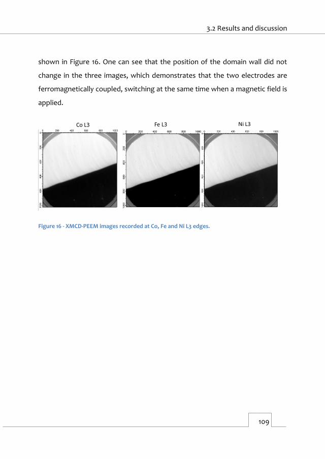
3.2 Results and discussion
109
shown in Figure 16. One can see that the position of the domain wall did not
change in the three images, which demonstrates that the two electrodes are
ferromagnetically coupled, switching at the same time when a magnetic field is
applied.
Figure 16 - XMCD-PEEM images recorded at Co, Fe and Ni L3 edges.

3 Functionalization of metallic ferromagnetic surfaces
110
3.2.4. Extending the functionalization
We continued the study of the formation of longer alkanethiol SAMs on Co and
Py using the mixing methodology. We functionalized three Co and Py
substrates with alkanethiols from 1-tetradecanethiol (C14S) to 1-
octadecanethiol (C18S) and measured wθCA after 16 h. The average results for
both surfaces are reported in table 5.
Table 5 - wθCA of functionalized Co and Py samples with different CnS
Molecule wθAA [º] wθRA[º] Hysteresis
Co-C14S 109 103 6
Co-C16S 112 104 8
Co-C18S 118 105 13
Py-C14S 111 102 9
Py-C16S 113 103 10
Py-C18S 116 105 11
A dependence of the contact angle with the chain length can be clearly
observed. As shown in the chapter 2 for APA SAMs, the clear progression of the
contact angle is related with an increase of the quality of the SAM as the alkyl
chain length increases. However, we observed that the hysteresis in the wθCA,
follow an unexpected trend with respect of the SAMs formed in the previous
chapter. Usually when the chain used to form a SAM is longer, the hysteresis is
smaller. In our case we observe for both surfaces that the hysteresis increases
with the chain length.

3.2 Results and discussion
111
Figure 17 - AFM topographic images of Co functionalized with: a) C12S, b) C14S, c) C16S and d) C18S. The scale bar is 5 µm.
When we examined the set of Co and Py samples functionalized with
alkanethiol (C12S–C18S) using the AFM under ambient conditions, we noticed
that despite the air exposed C12S sample presented a smooth surface,
comparable to that measurement carried in the glove box, upon air exposure
of C14S, C16S and C18S samples, lamellar domains were formed on the surface.
Similar results were obtained also for Py. The next chapter will be focused on
the characterization of these features.

3 Functionalization of metallic ferromagnetic surfaces
112
3.2.5. Fabrication of MTJ devices based on FM electrodes and SAMs
As introduced before, I did a 3 months stay at the UMR137 in Palaiseau under
the supervision of Prof. Pierre Seneor and Dr. Richard Mattana. During this
period I learned how to prepare spintronic devices using the nanoindentation
assisted by AFM technique, which had been successfully used before for the
preparation of LSMO//CnP/C0 devices.25–27 We wanted to test if the
combination of chemical oxide etching, developed above, and AFM assisted
nanoindentation was valid to prepare Co,Py//CnS/FM MTJs.
The technique, represented in Figure 18, is based on four steps: i) deposition by
spin-coating of a resistive polymer matrix on the air oxidized FM surface, ii)
nanoholes are fabricated by indentation, with the help of the AFM, iii) on the
exposed surface the native oxide etching process with GA and the alkanethiol
functionalization are carried out inside a glove box, iv) the last step is the
evaporation of the top electrode without breaking the controlled atmosphere.
The nanoindentation is performed using a modified conductive tip AFM, which
monitors in real time the resistance between the tip and the FM electrode. The
photoresist used is highly resistive, and depending on the depth reached the
resistance changes drastically. This enables a high control on the contact made
during the fabrication. With this technique the risk of short-circuit of the device
is decreased due to the small area (20 nm2) of each contact.
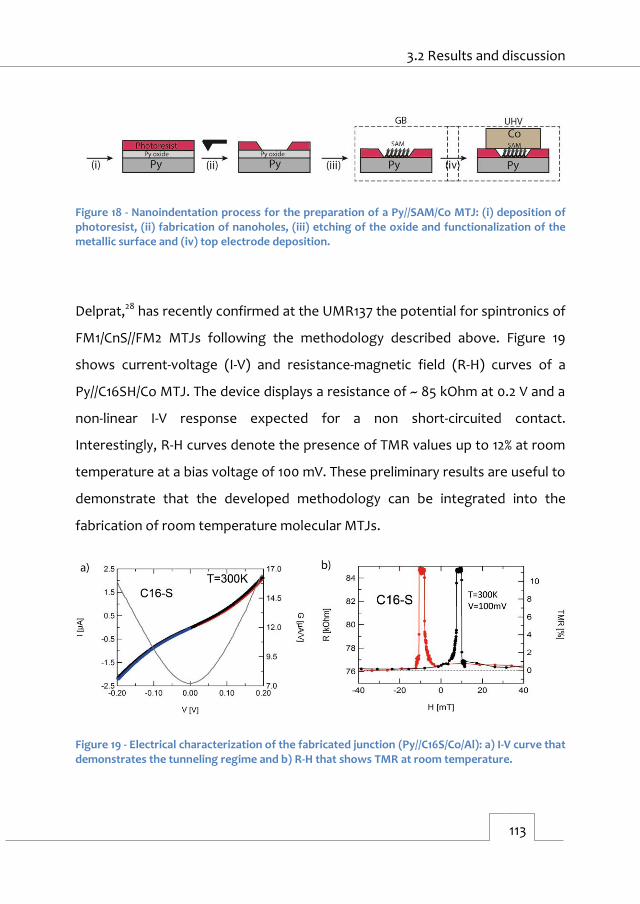
3.2 Results and discussion
113
Figure 18 - Nanoindentation process for the preparation of a Py//SAM/Co MTJ: (i) deposition of photoresist, (ii) fabrication of nanoholes, (iii) etching of the oxide and functionalization of the metallic surface and (iv) top electrode deposition.
Delprat,28 has recently confirmed at the UMR137 the potential for spintronics of
FM1/CnS//FM2 MTJs following the methodology described above. Figure 19
shows current-voltage (I-V) and resistance-magnetic field (R-H) curves of a
Py//C16SH/Co MTJ. The device displays a resistance of ~ 85 kOhm at 0.2 V and a
non-linear I-V response expected for a non short-circuited contact.
Interestingly, R-H curves denote the presence of TMR values up to 12% at room
temperature at a bias voltage of 100 mV. These preliminary results are useful to
demonstrate that the developed methodology can be integrated into the
fabrication of room temperature molecular MTJs.
Figure 19 - Electrical characterization of the fabricated junction (Py//C16S/Co/Al): a) I-V curve that demonstrates the tunneling regime and b) R-H that shows TMR at room temperature.

3 Functionalization of metallic ferromagnetic surfaces
114
3.3. Conclusions
We have developed a novel methodology to recover already oxidized
ferromagnetic Co and Py surfaces by selectively removing the native oxide by
means of a wet chemical etching with GA. This process avoids the use of
complicated UHV approaches or physical methods and is compatible with
common lithographic techniques. We have characterized both etched surfaces
by means of different characterization techniques such as XRR, XPS and SQUID
magnetometry to check that this treatment does not affect the properties of
the metallic bulk. Then, we have moved towards the functionalization of the
surfaces with alkanethiols. We have observed that if the functionalized
surfaces are kept in inert atmosphere it is possible to use this method to build
molecular spintronic devices, which exhibit tunnel magnetoresistance at room
temperature. However, if these surfaces are exposed to air, lamellar domains
start appearing on it. The characterization of these strange and unexpected
features will be described in the next chapter.

3.4 References
115
3.4. References
1. Finazzi, M., Duò, L. & Ciccacci, F. Magnetic properties of interfaces and
multilayers based on thin antiferromagnetic oxide films. Surf. Sci. Rep.
64, 139–167 (2009).
2. Sanvito, S. Molecular spintronics: The rise of spinterface science. Nat.
Phys. 6, 562–564 (2010).
3. Galbiati, M. et al. Spinterface: Crafting spintronics at the molecular scale.
MRS Bull. 39, 602–607 (2014).
4. Nuzzo, R. G., Fusco, F. A. & Allara, D. L. Spontaneously organized
molecular assemblies. 3. Preparation and properties of solution
adsorbed monolayers of organic disulfides on gold surfaces. J. Am.
Chem. Soc. 109, 2358–2368 (1987).
5. Schoenfisch, M. H. & Pemberton, J. E. Air stability of alkanethiol self-
assembled monolayers on silver and gold surfaces. J. Am. Chem. Soc. 120,
4502–4513 (1998).
6. Hutt, D. A. & Liu, C. Oxidation protection of copper surfaces using self-
assembled monolayers of octadecanethiol. Appl. Surf. Sci. 252, 400–411
(2005).
7. Devillers, S., Hennart, A., Delhalle, J. & Mekhalif, Z. 1-Dodecanethiol Self-
Assembled Monolayers on Cobalt. Langmuir 27, 14849–14860 (2011).

3 Functionalization of metallic ferromagnetic surfaces
116
8. Hoertz, P. G., Niskala, J. R., Dai, P., Black, H. T. & You, W. Comprehensive
Investigation of Self-Assembled Monolayer Formation on Ferromagnetic
Thin Film Surfaces. J. Am. Chem. Soc. 130, 9763–9772 (2008).
9. Mekhalif, Z., Riga, J., Pireaux, J.-J. & Delhalle, J. Self-Assembled
Monolayers of n-Dodecanethiol on Electrochemically Modified
Polycrystalline Nickel Surfaces. Langmuir 13, 2285–2290 (1997).
10. Galbiati, M. et al. Recovering ferromagnetic metal surfaces to fully
exploit chemistry in molecular spintronics. AIP Adv. 5, (2015).
11. Senthil kumar, K. et al. Fabrication of ultra-smooth and oxide-free
molecule-ferromagnetic metal interfaces for applications in molecular
electronics under ordinary laboratory conditions. RSC Adv. 7, 14544–
14551 (2017).
12. Vogt, A. D., Han, T. & Beebe, T. P. Adsorption of 11-Mercaptoundecanoic
Acid on Ni(111) and Its Interaction with Probe Molecules. Langmuir 13,
3397–3403 (1997).
13. Rajalingam, S., Devillers, S., Dehalle, J. & Mekhalif, Z. A two step process
to form organothiol self-assembled monolayers on nickel surfaces. Thin
Solid Films 522, 247–253 (2012).
14. Caipa Campos, M. A. et al. Self-Assembled Functional Organic
Monolayers on Oxide-Free Copper. Langmuir 27, 8126–8133 (2011).
15. Smardz, L., Köbler, U. & Zinn, W. Oxidation kinetics of thin and ultrathin
cobalt films. J. Appl. Phys. 71, 5199–5204 (1992).

3.4 References
117
16. Svalov, A. V et al. Influence of temperature on structure and magnetic
properties of exchange coupled TbCo/FeNi bilayers. J Nanosci
Nanotechnol 12, 7566–7570 (2012).
17. Nahrwold, G. et al. Structural, magnetic, and transport properties of
Permalloy for spintronic experiments. J. Appl. Phys. 108, 13907 (2010).
18. Pollak, R. A. & Bajorek, C. H. Surface composition and chemistry of
evaporated Permalloy films observed by x−ray photoemission
spectroscopy and by Auger electron spectroscopy. J. Appl. Phys. 46,
1382–1388 (1975).
19. Mekhalif, Z., Laffineur, F., Couturier, N. & Delhalle, J. Elaboration of Self-
Assembled Monolayers of n-Alkanethiols on Nickel Polycrystalline
Substrates: Time, Concentration, and Solvent Effects. Langmuir 19, 637–
645 (2003).
20. Greenler, R. G. Infrared Study of Adsorbed Molecules on Metal Surfaces
by Reflection Techniques. J. Chem. Phys. 44, 310–315 (1966).
21. Nuzzo, R. G. & Allara, D. L. Adsorption of bifunctional organic disulfides
on gold surfaces. J. Am. Chem. Soc. 105, 4481–4483 (1983).
22. Schreiber, F. Structure and growth of self-assembling monolayers. Prog.
Surf. Sci. 65, 151–256 (2000).
23. Petrovykh, D. Y. et al. Alkanethiols on platinum: multicomponent self-
assembled monolayers. Langmuir 22, 2578–87 (2006).

3 Functionalization of metallic ferromagnetic surfaces
118
24. Lee, J. R. I. et al. X-ray absorption spectroscopy for the structural
investigation of self-assembled-monolayer-directed mineralization.
Methods Enzymol. 532, 165–187 (2013).
25. Bouzehouane, K. et al. Nanolithography Based on Real-Time Electrically
Controlled Indentation with an Atomic Force Microscope for
Nanocontact Elaboration. Nano Lett. 3, 1599–1602 (2003).
26. Tatay, S. et al. Self-assembled monolayer-functionalized half-metallic
manganite for molecular spintronics. ACS Nano 6, 8753–8757 (2012).
27. Galbiati, M. et al. Unveiling self-assembled monolayers’ potential for
molecular spintronics: Spin transport at high voltage. Adv. Mater. 24,
6429–6432 (2012).
28. Delprat, S. Jonctions tunnel magnétiques avec des monocouches
moléculaires auto-assemblées. (Université Pierre et Marie Curie, 2017).

119
4. Characterization of
lamellar alkanethiolate
domains on
ferromagnetic surfaces
4.1. Introduction
In the previous chapter, we have studied a novel method to recover oxidized
Co or Py FM surfaces under inert conditions using GA to selectively etch the
native oxide leaving a clean metallic surface. As summarized in Figure 1, the
new exposed material was chemically active and could be functionalized with
alkanethiols of different chain lengths (CnS n= 12, 14, 16 and 18). The resulting
SAMs were stable for days under inert atmosphere. However, when these
functionalized surfaces (CnS with n>12) were exposed to the air, island-like
domains that could be easily distinguished by optical microscopy rapidly appear
on the surface.
4
0

4 Characterization of lamellar alkanethiolate domains on ferromagnetic surfaces
120
Figure 1 – a) Pictorial representation of island-like domain formation on an alkanethiol functionalized FM sample: i) Etching of native oxide layer on the FM with GA, ii) grafting of the CnS SAM, iii) functionalized films stable under inert atmosphere, iv) islands grow as the sample is exposed to air. b-c) Optical images of a functionalized Co surface with C14S just after functionalization (b) and after 16h of air exposure (c).
When we studied the islands formed on our samples with more detail by AFM
(Figure 2) we noticed that these domains show a layered structure, as
highlighted by the height distribution represented in Figure 2c. Although, the
formation of oxide islands on some bare metals, such as aluminium1 and cobalt2
had been reported previously in literature, the fact that our reference samples
(i.e. prepared exactly the same way but without thiol SAM) do not evolve into
islands formation motivated us to look for alternative explanations about the
nature of the observed features.
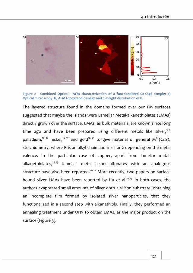
4.1 Introduction
121
Figure 2 - Combined Optical - AFM characterization of a functionalized Co-C14S sample: a) Optical microscopy. b) AFM topographic image and c) height distribution of b.
The layered structure found in the domains formed over our FM surfaces
suggested that maybe the islands were Lamellar Metal-alkanethiolates (LMAs)
directly grown over the surface. LMAs, as bulk materials, are known since long
time ago and have been prepared using different metals like silver,3–9
palladium,10–14 nickel,15–17 and gold18–21 to give material of general Mn+(CnS)n
stoichiometry, where R is an alkyl chain and n = 1 or 2 depending on the metal
valence. In the particular case of copper, apart from lamellar metal-
alkanethiolates,24,25 lamellar metal alkanesulfonates with an analogous
structure have also been reported.26,27 More recently, two papers on surface
bound silver LMAs have been reported by Hu et al.22,23 In both cases, the
authors evaporated small amounts of silver onto a silicon substrate, obtaining
an incomplete film formed by isolated silver nanoparticles, that they
functionalized in a second step with alkanethiols. Finally, they performed an
annealing treatment under UHV to obtain LMAs, as the major product on the
surface (Figure 3).

4 Characterization of lamellar alkanethiolate domains on ferromagnetic surfaces
122
Figure 3 - Figure extracted from reference 23, which displays the formation of LMAs from silver nanoparticles.
LMA structure is generally described as formed by the stacking of slabs with a
central metal-sulfur backbone, sandwiched between two alkyl chains, as
represented in Figure 4.
Figure 4 - SEM image of a Ag(CnS) LMA extracted from ref 8 (n = 16). Cartoon representing the structure of a M(SR)2 lamellar metal-alkanethiolate. The thickness of a single LMA slab is the result of the contributions from the methylene chain (dCH2), terminal methyl group (dCH3), carbon-sulfur (dC-S) and metal-sulfur (dSap) bond distances.

4.1 Introduction
123
The scope of this chapter will be to elucidate by means of different surface
techniques if the real nature of the domains spontaneously formed over our
FM substrates correspond to that of LMA and to try to understand the origin
and factors controlling the growing process.
4.2. Results and discussion
4.2.1. Structural Studies
In order to perform a detailed study about the structure of the domains, first
we used AFM to obtain local quantitative topographic 3D information. Figure 5
shows the topographic images and the corresponding height distributions of
islands formed from C14S, C16S and C18S alkanethiol samples. In all cases, the
presence of multiple levels with defined step height is evidenced.

4 Characterization of lamellar alkanethiolate domains on ferromagnetic surfaces
124
Figure 5 - AFM topographic images and height distribution profiles of islands obtained with C14S (a and d), C16S (b and e) and C18S (c and f). The difference between the black lines corresponds to the step heights. The scale bar is of 5 µm.
By measuring step heights (SH) on at least 6 islands of each chain length on Co
and Py, we obtained an estimation of the most probable step height for each
case (Figure 6b). Although no remarkable differences between equivalent SAM
functionalized Co and Py samples were noticeable, a clear increase with the
number of carbon atoms was observed, indicating that the islands contain
alkanethiol chains. Thus, the islands formed from C14S show an average step
height of 3.6 nm, which increases to 4.1 nm for those based on C16S and finally
to 4.5 nm for those based on a C18S (Figure 6 and Table 1).

4.2 Results and discussion
125
Figure 6 – a) Step height versus chain length of M-CnS island domains determined from AFM (red dots, M = Co and Py) and XRD (blue dots, M = Co). Solid lines are linear fits to the data (SH = mC + b, C = number of carbons). Fitted values are displayed as an inset. b) Step height distribution obtained after measuring individual step heights in 6 islands of each chain length on Co and Py. AFM error bars in a) are calculated as Gaussian fit from b). The error bars for XRD were calculated from the average of at least 2 different XRD measurements as those displayed in Figure 7.
As can be seen, there is a clear dependence between the alkanethiol chain
length and the step height of the obtained islands, which indicates that the
materials share a common structure.5,7
In order to have a further experimental proof on the layered nature of the
island domains and the step height values, we also run a series of out-of-plane
XRD measurements at Diamond Light Source BI07 beam line. To minimize FM
layer contribution, we covered several silicon substrates with only 4 nm of
cobalt (usually we worked with 15 nm thickness). Then samples were
functionalized with C14S, C16S and C18S, exposed to the air and the XRD data
recorded. Representative diffractograms are showed in Figure 7.

4 Characterization of lamellar alkanethiolate domains on ferromagnetic surfaces
126
Figure 7 – Out-of-plane XRD measurements on Co-CnS samples: C14S (red), C16S (black) and C18S (blue).
We observe for all the samples three equally spaced diffraction peaks. The
interlayer spacing determined from this periodicity, after applying the Bragg’s
law (2𝑑𝑠𝑖𝑛𝜃 = 𝑛𝜆),28 with n equal to 1 and λ equal to 0.9918 Å (C18S Δ2θ = 2.47
deg; d = 23 Å, C16S Δ2θ = 2.64; d = 21.50 Å, C14S Δ2θ = 3.07; d = 18.5 Å) closely
correspond to half of the step height determined by AFM (Figure 6, blue dots).
Table 1 - Step height estimated from AFM and XRD measurements and predicted all-trans SAM thickness. The XRD Step heights have been calculated as two times the interlayer spacing determined from XRD measurements.
Material AFM Step Height [nm] XRD Step Height [nm] SAM thickness [nm]
M-C14S 3.6 3.7 1.7
M-C16S 4.1 4.3 1.9
M-C18S 4.5 4.6 2.1

4.2 Results and discussion
127
Next, we studied the average height of the islands. From the AFM height
distribution measured in at least 5 samples of each chain length over Co and Py
and considering the average step height for a C14S, C16S and C18S alkyl chain
equal to 3.6 nm, 4.1 nm and 4.6 nm, respectively, as obtained from the
experimental data, we computed the height (number of layers) histograms
represented in Figure 8. Yellow dashed lines in this figure are the histogram
integrals.

4 Characterization of lamellar alkanethiolate domains on ferromagnetic surfaces
128
Figure 8 - AFM height statistics of island features: C14S(red), C16S (black) and C18S (blue). Yellow dashed line corresponds to the integral of the histogram.
From the histograms, we extracted the average height of the islands formed
for each alkyl chain and P85 and P50. P85(50) represents the island height below
which 85(50)% of observations fall. Analyzing P85 values presented in Table 2,
for Co and Py, there is a clear trend: C14S islands are thicker while C18S in most

4.2 Results and discussion
129
cases are formed by a single layer. Moreover, islands of Co are thinner than
those observed on Py.
Table 2 – Statistical parameters from histograms in Figure 8.*Number of layers values are calculated from P85.
Material Average Height [nm] P85 [nm] Number of layers* P50 [nm]
Co-C14S 12.2 18 5 7.2
Co-C16S 18.5 16.4 4 10
Co-C18S 4.6 4.6 1 -
Py-C14S 19.8 39.6 11 25.2
Py-C16S 14.2 20.5 5 4.1
Py-C18S 4.6 4.6 1 -
The above results support that: i) alkyl chains form part of the structure of the
lamella, ii) our lamellae present out-of-plane crystallinity and iii) the assembly of
alkyl thiol chains results in the formation of layered structures with step heights
fixed by the length of the organic molecules, which will be in accordance with
the LMA structure proposed in Figure 4.
Moreover, this clear dependence with the alkyl chain length rules out the idea
of metal oxide as main component of the islands and supports the possibility
that during the oxidation of the surface beneath the formed SAM (air
exposure), there is a reorganization of the organic molecules into lamellar
alkanethiolate domains formed by metal ions, extracted from the metal
surface, upon oxidation which are coordinated by the organic molecules.

4 Characterization of lamellar alkanethiolate domains on ferromagnetic surfaces
130
If we assume that our islands are in fact the result of the growth of LMAs
directly on surfaces, as suggested by the observed dependence of the step
height on the chain length, it is possible to build a structural model based on
step height data, represented in Figure 4. The total Step Height should be the
sum of the contributions coming from: 1) the methylene chain ((n-2)·dCH2),
being dCH2 the vertical C-C distance and n the number of carbons in the chain
and 2) d0, that represents the contribution provided by the sum of the distance
from the S atom to the metal plane (dSap), the C-S bond distance (dC-S) and the
terminal methyl group (dCH3). That is:
Step Height=2·[(n-2)·dCH2 + d0]
d0 = dSap + dC-S + dCH3
We used the results from the linear fitting of the AFM step height displayed in
Figure 4 to obtain the following values: dCH2 = m = 0.22 nm and 2d0= b+2dCH2 =
0.917 nm. Assuming that the CH2 groups in the alkyl chain are fully stretched,
and taking into account that the theoretical carbon-carbon vertical distance is
dC-C = 0.127 nm,7 from dCH2 we can estimate a chain tilt angle of 30º. This value is
close to the expected value for close packed alkyl chains on gold.29 From the
theoretical carbon sulfur bond length dC-S = 0.182 nm,8 and the theoretical van
der Waals radii of the methyl group dCH3 = 0.21 nm,8 which is calculated from the
average value of the distance between the carbon located before the methyl
carbon and the last hydrogen(s) that points up to the next layer, we can derive
dSap = 0.068 nm.

4.2 Results and discussion
131
In Table 3 we summarize the dCH2 and 2d0 values calculated from the Step
Heights reported in the literature for bulk nickel, palladium and silver LMAs. As
can be observed our values are not far from some of those previously reported.
Table 3 - dCH2 and dCH2 obtaianed from our AFM and XRD data compared with values obtained from the literature for bulk LMAs.
Material dCH2[nm] 2d0[nm] Tilt Angle [º] Ref Compound
Ni 0.258 0.78 0 16 Ni(SR)2
Pd 0.248 0.81 14 14 Pd(SR)2
Ag 0.248 0.98 14 5 AgSR
Ag 0.250 0.97 12 9 AgSR
Ag 0.241 1. 02 19 7 AgSR
Ag 0.242 1. 05 19 8,26,27 AgSR
Py/Co (AFM) 0.225 0.92 30 This thesis
Co (XRD) 0.225 1.05 30 This thesis
Additionally, we performed a search in the Cambridge Structural Database
(CSD) (23/11/2016) for motives including µ2S–M and µ3S–M bridges where M=Co,
Fe and Ni. From this query, we obtained 5739 and 43 hits, respectively. The
average values for dSap, in the case of µ2S–M and µ3S–M bridges, are
respectively 0.070 nm and 0.092 nm. Thus, we observed that our dSap value
calculated from AFM data (0.068 nm), matches with the crystallographic
database for µ2S–M bridges coordination. If we repeat the calculation using
XRD data, however, our final value for dSap is 0.133 nm, which would indicate
µ3S–M bridges. As a result, and due to the experimental error, we cannot

4 Characterization of lamellar alkanethiolate domains on ferromagnetic surfaces
132
extract further information about sulfur coordination in island domains.
Nevertheless, we can assume that S is µ3-coordinated and that binds to the
metal plane forming a regular pyramid with a triangular base. These will result
in a distorted hexagonal network packing, formed by octahedral MS6 sites
showing edges with half of the S atoms above and below the plane formed by
the M atoms, as represented in Figure 9. This kind of packing is the same that
the one adopted by layered double hydroxides (LDHs) and by hexagonal
transition metal dichalcogenides (TMDCs).
Figure 9 – a) Top view of a schematic representation of the metal-sulfur regions. Metal atoms are represented in red, sulfur atoms above and below the backbone plane are in yellow and b) octahedral coordination of the metal atom.
Next, we will analyze the amount of material that migrates from the interfacial
SAM to form the lamellar structures during the growing process. For the case
of C18S, the calculations are easier. In the Figure 10, the islands present on the
cobalt surface functionalized with C18S have 3 layers with defined heights: the
first one has 3.8 nm, and the second and the third ones, 8.4 and 13 nm,
respectively. These layers cover respectively 16%, 2.35 % and 0.70% of the total

4.2 Results and discussion
133
image area. Assuming that the area per molecule is the same in an island and in
the original SAM, in order to calculate the total equivalent coverage, we need
to multiply each value respectively by 2, 4 and 6 and sum all the resulting areas,
which gave us an equivalent coverage value of 45.62%. This result means that
only about 50% of the molecules that composed the original SAM have
migrated into the island, and that the space between the islands is not
completely void. Unfortunately, this simple analysis cannot be carried out for
C14 and C16 samples because the number of islands imaged in a convectional
AFM pictures is not high enough to obtain meaningful values. Another
interesting thing that can be observed from the height histogram in Figure 10d,
is the presence of the first peak at 3.8 nm for the case of C18S, when the
calculated value for the step height is of 4.6 nm. This suggests the presence of
partial interdigitation between the island domains and the SAM beneath. This
behaviour is only observed with this chain length.

4 Characterization of lamellar alkanethiolate domains on ferromagnetic surfaces
134
Figure 10 - AFM images of islands grown on Co from different alkanethiolates with their respective height histogram: C18S (a-d) , C16S (b-e) and C14S (c-f). The scale bar is of 5 µm.
4.2.2. Area distribution studies
The islands domains were also imaged using microscopy techniques other than
AFM (i.e. Optic and SEM) in order to gain further information on their width
distributions and to estimate coverage values. Figure 11 shows images of a C14S
island grown on Py taken by means of atomic force, optical and scanning
electron microscopies. As can be seen, the height contrast observed in the
optical images is very weak (Figure 11b), but when the amount of light that
reaches the detector is reduced by means of a neutral-density filter (ND) it
improves considerably (Figure 11c). The alternative use of SEM was not so
effective, (Figure 11d) as these images showed poorer height contrast.
Moreover, we observed material damage after prolonged electron beam
exposure, using 20 kV as acceleration voltage.

4.2 Results and discussion
135
Figure 11 – A C14S island on Py imaged with different techniques a) AFM, b) Optical Microscope, c) Optical Microscope with ND Filter and d) SEM.
Although AFM is a very precise technique, and the only one that really gives
true topographic information of the sample, it is not suited to study large
surface areas (above 50-100 µm2), and for that reason we used optical
microscopy to study domain size distributions.
To perform a statistical analysis, first we prepared 3 Co and 3 Py samples with
SAMs of each chain length (CnS, n= 14, 16 and 18) and imaged at least 3
different areas of each sample using optical microscopy. Representative optic
images are showed in Figure 12. At a first glance, it is possible to observe that
alkyl chain length has an important influence on the size and number of the
formed domains.

4 Characterization of lamellar alkanethiolate domains on ferromagnetic surfaces
136
Figure 12 - Representative 100x optic images of Co and Py functionalized samples.

4.2 Results and discussion
137
Using an imaging processing software (Gwyddion31) we calculated domain area
histograms for each chain length. For the C14S and C16S we used 433x380 µm2
images, while for C18S we used 253x190 µm2 images. Results are presented in
Figure 13.
Figure 13 - Optical domain area histograms of Co and Py samples functionalized with C14s, C16S and C18S. Yellow dashed line is the area integral.

4 Characterization of lamellar alkanethiolate domains on ferromagnetic surfaces
138
Values displayed below show that for Co and Py, shorter chain lengths give rise
to bigger islands. However, less islands are detected on Py and tend to be
smaller than those found on Co for all chain lengths. Moreover, and according
to Table 2, longer alkyl chains render not only smaller but also thinner domains.
Table 4 – Statistical parameters from histograms in Figure 13 and total coverage derived from the optic statistic.
Material Average Area
[µm2]
Number of
Island/100 µm2
P85
[µm2]
P50
[µm2]
Coverage
[%]
Co-C14S 87.5 6.63 80 35 5.8
Co-C16S 22.5 33.8 20 10 7.6
Co-C18S 7.5 320 - - 24
Py-C14S 67.5 2.07 70 10 1.4
Py-C16S 7.5 30.7 15 5 2.3
Py-C18S 9 62.2 - - 5.6
From the analysed optical images, we also extracted the percentage of area
covered by the islands. As can be observed in Table 4 moving from the C14S to
the C18S, the cobalt coverage increases from approximately 6% to 24%.
Moreover, the measured coverage in the case of Py was always below that
measured for Co, and never exceeded 6%.
4.2 Results and discussion
139
Using the average height derived from AFM (Table 2) and the coverage values
displayed in Table 4, we can make a rough calculation of the material that has
displaced from the original SAM into the island domains:
𝐷 = 2 ∗ℎ̅
𝑆𝐻∗ 𝐶
Where D is the percentage of displaced material, ℎ̅ is the average island height,
SH is the calculated step height for each chain length and C is the coverage. We
obtain that for Co, D values for C14S, C16S and C18S are 39.3%, 68.5% and 48%,
respectively. The calculated value for C18S on cobalt is very close to the value
of 45.6 % calculated from AFM data in Figure 10. For the case of Py, the values
are 15.4%, 15.9% and 11.2%. These lower values reflect the lower tendency of Py
to form island domains. In any case, what seems clear is that the space
between islands is not completely void, and that there are still SAM molecules
present on the surface.
4.2.3. Spectroscopy studies
Auger Spectroscopy. To gain chemical information and further confirm the
structure proposed above we performed AES analysis on our samples in
collaboration with the Autonomous University of Barcelona (UAB). Figure 14a-b
shows a topographic AFM image of a C14S island of approximately 15 nm
height. According to the model proposed above, this will correspond to at least
3 RS-M-SR layers. We recorded AES data inside (red square) and outside the
island (green square) showed in Figure 14a. In Figure 14c-e the Auger spectra
obtained from these two zones are shown at the cobalt, oxygen and sulphur
edges. Outside the island strong oxygen and cobalt signals are recorded, while

4 Characterization of lamellar alkanethiolate domains on ferromagnetic surfaces
140
only a faint signature of sulphur can be observed. This data is consistent with
the migration towards the islands of surface bound thiols during the growing
process, exposing the cobalt surface to oxidation. When the measurement was
done on top of an island, we observed that the signals of cobalt and oxygen
were attenuated while sulphur signal slightly increased. Escape depth of Auger
electrons is only some nanometers, so the detector mostly collected electrons
originated at the island volume while signals coming from the underlying cobalt
surface are strongly attenuated. The main conclusion obtained from the AES
measurements is that the islands contain cobalt besides the sulphur of the
alkanethiol molecules. The presence of cobalt and sulfur inside the islands is
consistent with the structure proposed in Figure 9. We tried to repeat the
measurement in Py islands, to see if in the composition both nickel and iron
were present. However, we did not observe any difference from the signal
inside or outside the islands. This might indicate that the material was damaged
by the measurement.

4.2 Results and discussion
141
Figure 14 - Auger spectra determined inside (red) and outside (green) a C14S island grown over a 15 nm Co substrate, b) the height profile of the measured zone. Elemental spectra of c) Cobalt, d) Oxygen and e) Sulphur. The scale bar is of 2 µm.
Confocal Raman Spectroscopy. Strong adventitious carbon signals were
observed inside and outside the islands, hindering carbon edge interpretation.
Raman spectroscopy measurements were carried out to shine light on that, as
alkyl chains show characteristic Raman peaks.
We compared the spectra recorded inside and outside the islands. Data
recorded outside the island did not show any additional peaks compared to
non-functionalized reference air-exposed cobalt samples. We have also run a
series of measurements on gold surfaces functionalized with alkanethiols, but
we did not observe any Raman signal, which suggest that our Raman is not
sensitive enough to detect organic species at the monolayer level. Coming back
to our samples, this does not mean that outside the islands the SAM is absent.
From the data measured inside the island we observed a peak at 743 cm-1

4 Characterization of lamellar alkanethiolate domains on ferromagnetic surfaces
142
(Figure 15-i) that we tentatively assign to the twisting of the sulphur-carbon
bond. 3,32,33 Additionally, in Figure 15-ii, are displayed signals coming from the C–
H vibrations: C-H stretching (2849–2924 cm-1), CH2 scissoring (1450 cm-1) and C–
C aliphatic chain vibrations (1120–1290 cm-1).3,32,33 However, data measured
inside the island showed no trace of unbound S-H groups at 2575 cm-1 (Figure
15-iii). 3,32,33 The intense silicon substrate signals, strong peaks at 1000 cm-1, 532
cm-1 and 350 cm-1 mask any possible signal related to the S-M bonds which
should be expected below 400 cm-1.3,32,33 These results seem to confirm the
scenario were R-S molecules self-assembled on the cobalt surface, migrate and
accumulate in the form of island domains when exposed to air.

4.2 Results and discussion
143
Figure 15 - Raman spectra recorded inside and outside an island, with its insets i), ii) and iii) of the regions of interest. Peaks marked with an * come from the silicon substrate.
The results presented above further confirm that the lamellar domains
obtained after air exposure of Py and Co CnS–functionalized samples where
n=14, 16, 18 are indeed formed by LMAs.
4.2.4. Growth rate studies
In the previous paragraphs we showed the topographic, structural and
spectroscopy characterization of fully grown island domains. In this section, we
will study the growth of the island domains as a function of time and also we
will study the role of the temperature and atmosphere.

4 Characterization of lamellar alkanethiolate domains on ferromagnetic surfaces
144
We proceeded to functionalize a Co surface with C18S inside a glove box, then
we exposed the sample to air and we monitored the change of the topography
as a function of time of a 30x30 µm2 area using AFM. These results are
presented in Figure 16.
Figure 16 - Real time growth of C18S-Co island domains, imaged with AFM: AFM topographic images at 20 min (red), 2.5 h (orange), 5 h (yellow), 8 h (light green), 14.75 h (light blue), 15h (blue), 16.75 h (purple) and 20.65 h (deep red). (a) Evolution of the island coverage with time and (b) evolution of the height profile with time.

4.2 Results and discussion
145
Figure 16a represents the coverage changes during the growing process. The
AFM images with a coloured frame correspond to the points of the same colour
in Figure 16a. It is possible to observe that right after air exposition the island
domains started growing on the surface. The overall evolution of the height
distribution is reported in Figure 16b. We observed that in the first 20 min (red)
domains of around 4.5 nm height are present, while after 8 hours (green) some
domains with a height slightly above 9 nm (2 layers) appear, and finally at the
end of growing process, the height distribution reflects a small contribution of
domains with 13.5 nm (3 layers). As commented before, in the case of C18S
SAMs, interdigitation of the first layer is expected, which gives rise to a
difference in the step height of the first and consecutive layers. Sample imaged
in Figure 10 is not an exception of the above observation, but this effect is only
detected at the later stages of the growing process. For instance, it is clearly
visible after 17 hours (purple line) when no further evolution of number of
islands, their areas or their heights is observed.

4 Characterization of lamellar alkanethiolate domains on ferromagnetic surfaces
146
Figure 17 - Real time growth of C14S-Co island domains, imaged with AFM: AFM topographic images at 10 min (red), 1 h 10 min (blue), 2 h 20 min (orange), 3 h (dark green), 5 h 40 min (light blue), 8 h 50 min (pink), 10 h 40 min (purple) and 27 h 40 min (green). (a) Evolution of the island coverage with time and (b) evolution of the height profile with time. The colored squares indicate the corresponding point in the graph. The AFM images are 30x30 µm2.
We have imaged a Co sample functionalized with C14S using AFM, like in the
previous example. In this particular case, we observed a faster growth, because
the whole process is accomplished in around 10 hours, as can be seen in Figure
17a. The height distribution, presented in Figure 17b, shows the presence of
terraces of two layers (7 nm), since the very first images. After around 3h (in
dark green), higher steps can be also observed.

4.2 Results and discussion
147
Although some variability was observed between experiments, equivalent
assays revealed that between 10 and 16 hours are necessary to reach stable
island domains (no more variation in height or area are observed)
independently of the substrate (Co or Py) and chain length used (n = 14, 16 or
18).
This is the first time that a kinetic measurement in real time is reported for this
kind of island domains. We also want to remark that these island-like lamellar
domains, grow exclusively on Co and Py, at room temperature, in a solvent free
environment, which have never been reported in literature until the moment.
As we said before, AFM is a precise technique, but is time consuming and the
quick imaging of the samples during the very first seconds of air contact is not
possible. To improve the kinetic study, we took advantage of optical
microscopy in order to take large area pictures in a matter of seconds. This
allowed us to precisely follow the growing process in its initial stages. We
functionalized again a cobalt sample with C14S, the sample was exposed to air
and pictures were taken with the optical microscope every few minutes, as
showed in Figure 18-21.

4 Characterization of lamellar alkanethiolate domains on ferromagnetic surfaces
148
Figure 18 - Optical images of a kinetic on Co-C14S Surface from 0 to 35 minutes.
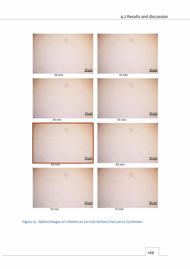
4.2 Results and discussion
149
Figure 19 - Optical images of a kinetic on Co-C14S Surface from 40 to 75 minutes.

4 Characterization of lamellar alkanethiolate domains on ferromagnetic surfaces
150
Figure 20 - Optical images of a kinetic on Co-C14S Surface from 80 to 115 minutes.

4.2 Results and discussion
151
Figure 21 - Selected Optical images of a kinetic on Co-C14S from 120 to 1980 minutes (33 hours).

4 Characterization of lamellar alkanethiolate domains on ferromagnetic surfaces
152
Figure 22 - Coverage evolution as a function of time of Co-C14S functionalized sample, calculated from images in Figure 18-21.
The coverage showed in Figure 22, exhibited the same trend of that measured
with AFM and displayed in Figure 16a. Due to the shorter acquisition time of
optical microscopy it is possible to observe that there is not only a lateral
growth of the islands but also a reorganization of the material inside the
growing domains. This is highlighted by the peak arising at 12o min in Figure 22.
4.2.5. Temperature and humidity influence studies
It is well known that the crystal growth in bulk materials is influenced by
various parameters such as temperature, concentration or the growing media
used.34 The temperature, in particular, influences the balance between the
nucleation and growth steps.35 Based on that idea and to prove if the same
behavior applies to our system, we performed a series of experiments where
Co-C14S freshly functionalized samples were exposed to air at different

4.2 Results and discussion
153
temperatures. We chose Co-C14S because, as discussed above, the resulting
island domains are bigger and their optical detection is easier.
We functionalized three cobalt samples with C14S and we exposed them to air
at three different temperatures: 35º, 25º (room temperature) and 5º and
recorded optic images for all of them, as represented in Figure 23.
Figure 23 – Optical images of a Co-C14S samples exposed to the air at different temperatures for 23h, with their correspondent area distribution histograms and histogram area integrals (yellow dashed line).
At a first glance, it is possible to observe that after 23 h, the area distribution
histograms show that an increase in temperature produces a smaller density of

4 Characterization of lamellar alkanethiolate domains on ferromagnetic surfaces
154
islands, but with bigger sizes (Table 5). This result suggests that island domains
grow following a nucleation and growth mechanisms similar to that observed
for other bulk solids in solution.
Table 5 - Statistical parameters for histograms in Figure 23
Temperature [º] Average Area [µm2] Number of Islands/100
µm2
P85 [µm2] P50 [µm2]
35 45 2.61 50 28
25 13 4.10 13 5
5 5 7.02 5 -
As we said before, one very important point is that, the LMAs growth take
place only when the samples are exposed to air and not when they are kept
under inert atmosphere. In ambient conditions, all surfaces are covered by a
thin film of water, with dimensions that depend on the nature of the surface
and the humidity and temperature conditions.36–38 We wanted to study if this
water layer was playing a key role in island domains formation. We designed an
experiment where we functionalized a set of two twin cobalt samples with
C14S. We exposed directly to air the first sample (Sample A), to have a
reference, while we transferred the second sample directly from the glove box
to a reaction chamber filled with dry air (Sample B). After 16 hours, we checked
both samples using optical microscopy (Figure 24), and left both of them
reacting in ambient conditions for additional 16 hours.

4.2 Results and discussion
155
Figure 24 - Optical images of the substrates subjected to air and dry air for 16h and 32h.
Area histograms of optical images represented in Figure 24 are displayed in
Figure 25.

4 Characterization of lamellar alkanethiolate domains on ferromagnetic surfaces
156
Figure 25 - Area distribution from the samples displayed in Figure 25 after 16h in air (or dry air) and additional 16 h in air. Yellow dashed line represents the histogram integrals.
In order to make straightforward the comprehension of the obtained results, in
table 6 are reported the number of islands and the P85 for each of the
atmospheres.

4.2 Results and discussion
157
Table 6 - Statistical parameters from histograms in Figure 25.
Sample Atmosphere Time
[h]
Average Area
[µm2]
Number of
Islands/ 100
µm2
P85
[µm2]
P50
[µm2]
A Air 16 10 5.31 8 2
Air 32 10 5.31 8 2
B Dry Air 16 2 3.86 2 1
Air 32 10 5.50 10 6
After 16h of reaction island growth on Sample A had already finished, and no
particular evolution is observed after 32h. In the case of Sample B, we also
observed the presence of islands after 16 hours of reaction under dry air.
However, when we further exposed the sample to air for additional 16 hours,
we found that both the number of island and their size increased to values
closer to that reported for Sample A. In conclusion, it seems that, although
water is not indispensable for island growth, it increases growth rate.
4.2.6. Etching Experiments
We took several topography AFM images on a single domain of Co-C18S in
tapping mode, and we noticed that the material was etched away, from image
to image, resulting in a modification of the island area. In the Figure 26l, it is
possible to observe that when all the material is taken away from the tip, on
the surface no hole is seen. This seems to confirm that island growth takes
place over the original SAM.

4 Characterization of lamellar alkanethiolate domains on ferromagnetic surfaces
158
Figure 26 – AFM topographic images of the Co-C18S island domains etching evolution depicted in a-l). The scale bar is 1 µm.
4.2.7. Growth mechanism
Based on all the information collected from the different techniques and from
the growth experiments, we can propose a model to explain how do the island
domains form. In Figure 27 our hypothesis is represented. In inert atmosphere,

4.2 Results and discussion
159
we functionalize the FM surface, forming a complete alkanethiolate SAM.
When the surface is exposed to air, oxygen reaches the cobalt surface through
defects in the monolayer (Figure 27,i) triggering the oxidation of the metal
from 0 to +2 and destabilizing the S-M bond. The continuity of the SAM is
broken, which gives rise to the “jumping” of the metallic oxidized ions with the
organic molecule away from the SAM giving rise to the appearance of the
islands (Figure 27,ii ).
Figure 27 - Proposed growth mechanism of surface island domains. When the functionalized sample is exposed to air (i), oxygen enters into the defects oxidating the metal. The SAM is broken and reorganizes itself into island domains, the mass movement follows (ii) forcing the island domains growth.

4 Characterization of lamellar alkanethiolate domains on ferromagnetic surfaces
160
4.3. Conclusions
The methodology studied in chapter 3 allowed the functionalization of FM
surfaces with alkanethiolate SAMs in inert conditions. We observed that when
these surfaces are exposed to air, lamellar domains started to appear
spontaneously, without the use of any external stimulus and in a solvent free
environment. The origin of their growth may be related to a not perfect
protection against oxidation provided by the SAM. Surprisingly, this behavior
has not been reported before in previous works that describe the preparation
of SAMs on FM metals, even though the quality of the formed SAMs is equal in
terms of contact angle, IR peaks value or stability against oxidation. Probably,
several reasons can justify this fact: (1) there are only few works that face the
formation of SAMs on FM metals, (2) imaging of the surface is usually not
provided, (3) these domains only appear after air contact and (4) their growth
seems to be restricted to alkanethiols chain lengths longer than 12 methylene.
Through this chapter, we have used several characterization techniques to
shine light on the composition of these lamellar features. AFM and XRR
confirmed that their step height is related to the alkanethiol used to
functionalize the surface. Combining these results with additional Raman and
AES spectroscopies, we have proposed an internal structure for the islands
formed by stacks of CnS-M-SCn layers, where M is the metal present on the FM
surface and CnS the thiol molecule. This structure is in resemblance to
previously reported bulk Lamellar Metal-alkanethiolates and to other layered
structures (LHDs and hexagonal TMDCs).

4.3 Conclusions
161
Our statistical analysis of AFM and Optical microscopy images pointed out that
the number, area and height of the islands are inversely proportional to the
length of the alkylic chain that composes the SAM. Moreover, in all cases not all
the thiol molecules migrate into the lamellae; part of them remain on the
surface as a SAM, which means that there is not bare surface between the
islands.
The study of the kinetics of the growing process has also been faced during this
chapter. These studies have confirmed that islands only start to appear when
the sample gets in contact with air, and that their evolution takes generally 10-
16 hours, after this time, no further changes are detected. It is also important
to remark that temperature strongly influences the process. An increase of the
temperature speeded up the assembly of the molecules, but the quality of the
obtained material was far below the room temperature one. We also observed
that the humidity of the environment does not play a critical role in the growth
of these lamellar features.
One remarkable feature emerged during the research, is that the islands
growth takes place in ambient conditions, at room temperature, in a solvent
free environment and without the use of any external stimulus.

4 Characterization of lamellar alkanethiolate domains on ferromagnetic surfaces
162
4.4. References
1. Hart, R. K. & Maurin, J. K. The nucleation and growth of oxide islands on
aluminum. Surf. Sci. 20, 285–303 (1970).
2. Luo, L., Kang, Y., Yang, J. C. & Zhou, G. Nucleation and growth of oxide
islands during the initial-stage oxidation of (100)Cu-Pt alloys. J. Appl.
Phys. 117, 65305 (2015).
3. Fijolek, H. G., Grohal, J. R., Sample, J. L. & Natan, M. J. A Facile Trans to
Gauche Conversion in Layered Silver Butanethiolate. Inorg. Chem. 36,
622–628 (1997).
4. Bensebaa, F., Ellis, T. H., Kruus, E., Voicu, R. & Zhou, Y. The self-assembly
of a layered material: metal-alkanethiolate bilayers. Can. J. Chem. 76,
1654–1659 (1998).
5. Bensebaa, F., Ellis, T. H., Kruus, E., Voicu, R. & Zhou, Y. Characterization
of Self-Assembled Bilayers: Silver−Alkanethiolates. Langmuir 14, 6579–
6587 (1998).
6. Levchenko, A. A., Yee, C. K., Parikh, A. N. & Navrotsky, A. Energetics of
Self-Assembly and Chain Confinement in Silver
Alkanethiolates: Enthalpy−Entropy Interplay. Chem. Mater. 17, 5428–
5438 (2005).
7. Dance, I. G., Fisher, K. J., Banda, R. M. H. & Scudder, M. L. Layered
structure of crystalline compounds silver thiolates (AgSR). Inorg. Chem.
30, 183–187 (1991).

4.4 References
163
8. Ye, Z., de la Rama, L. P., Efremov, M. Y., Zuo, J.-M. & Allen, L. H.
Approaching the size limit of organometallic layers: synthesis and
characterization of highly ordered silver–thiolate lamellae with ultra-
short chain lengths. Dalt. Trans. 45, 18954–18966 (2016).
9. Parikh, A. N. et al. Characterization of Chain Molecular Assemblies in
Long-Chain, Layered Silver Thiolates: A Joint Infrared Spectroscopy and
X-ray Diffraction Study. J. Phys. Chem. B 103, 2850–2861 (1999).
10. John, N. S., Thomas, P. J. & Kulkarni, G. U. Self-Assembled Hybrid
Bilayers of Palladium Alkanethiolates. J. Phys. Chem. B 107, 11376–11381
(2003).
11. John, N. S., Pati, S. K. & Kulkarni, G. U. Electrical characteristics of
layered palladium alkanethiolates by conducting atomic force
microscopy. Appl. Phys. Lett. 92, 13120 (2008).
12. Busupalli, B., Kummara, S., Kumaraswamy, G. & Prasad, B. L. V. Ultrathin
Sheets of Metal or Metal Sulfide from Molecularly Thin Sheets of Metal
Thiolates in Solution. Chem. Mater. 26, 3436–3442 (2014).
13. Yang, Z., Smetana, A. B., Sorensen, C. M. & Klabunde, K. J. Synthesis and
Characterization of a New Tiara Pd(II) Thiolate Complex,
[Pd(SC12H25)2]6 , and Its Solution-Phase Thermolysis to Prepare Nearly
Monodisperse Palladium Sulfide Nanoparticles. Inorg. Chem. 46, 2427–
2431 (2007).
14. Thomas, P. J., Lavanya, A., Sabareesh, V. & Kulkarni, G. U. Self-

4 Characterization of lamellar alkanethiolate domains on ferromagnetic surfaces
164
assembling bilayers of palladiumthiolates in organic media. J. Chem. Sci.
113, 611–619 (2001).
15. Woodward, P., Dahl, L. F., Abel, E. W. & Crosse, B. C. A New Type of
Cyclic Transition Metal Complex, [Ni(SC 2 H 5 ) 2 ] 6. J. Am. Chem. Soc. 87,
5251–5253 (1965).
16. John, N. S. et al. Magnetic Interactions in Layered Nickel Alkanethiolates.
J. Phys. Chem. C 111, 1868–1870 (2007).
17. Calderon, M. F. et al. New Findings for the Composition and Structure of
Ni Nanoparticles Protected with Organomercaptan Molecules. Langmuir
29, 4670–4678 (2013).
18. Cha, S.-H., Kim, J.-U., Kim, K.-H. & Lee, J.-C. Preparation and
Photoluminescent Properties of Gold(I)−Alkanethiolate Complexes
Having Highly Ordered Supramolecular Structures. Chem. Mater. 19,
6297–6303 (2007).
19. Cha, S.-H., Kim, K.-H., Kim, J.-U., Lee, W.-K. & Lee, J.-C. Thermal Behavior
of Gold(I)−Thiolate Complexes and Their Transformation into Gold
Nanoparticles under Heat Treatment Process. J. Phys. Chem. C 112,
13862–13868 (2008).
20. Nie, H., Li, M., Hao, Y., Wang, X. & Zhang, S. X.-A. Time-resolved
monitoring of dynamic self-assembly of Au(i)-thiolate coordination
polymers. Chem. Sci. 4, 1852 (2013).
21. Woodward, J. T. et al. Effect of an Oxidized Gold Substrate on

4.4 References
165
Alkanethiol Self-Assembly. Langmuir 16, 5347–5353 (2000).
22. Sandhyarani, N. & Pradeep, T. An investigation of the structure and
properties of layered copper thiolates. J. Mater. Chem. 11, 1294–1299
(2001).
23. Keller, H., Simak, P., Schrepp, W. & Dembowski, J. Surface chemistry of
thiols on copper: an efficient way of producing multilayers. Thin Solid
Films 244, 799–805 (1994).
24. Park, S.-H. & Lee, C. E. A series of long-chain lamellar hydrated copper(II)
alkylsulfonates with different chain molecular assemblies. Chem.
Commun. 1, 1838–1839 (2003).
25. Park, S. H. & Lee, C. E. Characterization of chain molecular assemblies in
long-chain, lamellar copper alkylsulfonates: Self-assembled monolayer
vs bilayer structure. Chem. Mater. 18, 981–987 (2006).
26. Hu, L. et al. Self-Assembly and Ripening of Polymeric
Silver−Alkanethiolate Crystals on Inert Surfaces. Langmuir 25, 9585–9595
(2009).
27. Hu, L. et al. Synthesis and Characterization of Single-Layer
Silver−Decanethiolate Lamellar Crystals. J. Am. Chem. Soc. 133, 4367–
4376 (2011).
28. Bragg, W. H. & Bragg, W. L. The Reflection of X-rays by Crystals. Proc. R.
Soc. A Math. Phys. Eng. Sci. 88, 428–438 (1913).

4 Characterization of lamellar alkanethiolate domains on ferromagnetic surfaces
166
29. Sellers, H., Ulman, A., Shnidman, Y. & Eilerss, J. E. Structure and Binding
of Alkanethiolates on Gold and Silver Surfaces: Implications for Self-
Assembled Monolayers. J. Am. Chem. SOC 115, 9389–9401 (1993).
30. Nečas, D. & Klapetek, P. Gwyddion: an open-source software for SPM
data analysis. Open Phys. 10, 181–188 (2012).
31. Bensebaa, F. et al. Raman characterization of metal-alkanethiolates.
Spectrochim. Acta Part A Mol. Biomol. Spectrosc. 55, 1229–1236 (1999).
32. Bryant, M. A. & Pemberton, J. E. Surface Raman scattering of self-
assembled monolayers formed from 1-alkanethiols: behavior of films at
gold and comparison to films at silver. J. Am. Chem. Soc. 113, 8284–8293
(1991).
33. Burton, W. K. & Cabrera, N. Crystal growth and surface structure. Part I.
Discuss. Faraday Soc. 5, 33 (1949).
34. Cabrera, N. & Burton, W. K. Crystal growth and surface structure. Part II.
Discuss. Faraday Soc. 5, 40 (1949).
35. Santos, S. & Verdaguer, A. Imaging Water Thin Films in Ambient
Conditions Using Atomic Force Microscopy. Materials (Basel). 9, 182
(2016).
36. Henderson, M. A. The interaction of water with solid surfaces:
fundamental aspects revisited. Surf. Sci. Rep. 46, 1–308 (2002).
37. Verdaguer, A., Sacha, G. M., Bluhm, H. & Salmeron, M. Molecular

4.4 References
167
structure of water at interfaces: Wetting at the nanometer scale. Chem.
Rev. 106, 1478–1510 (2006).

168

169
Conclusions and Outlook
After our exhaustive study about the molecular functionalization of
ferromagnetic metals, several aspects can be highlighted as main conclusions
of this work that will drive the perspectives of our future working plan:
1- The passivating oxide layer that naturally grows on FM metals in ambient
conditions can be used as adhesion layer for the growth of high quality SAMs.
The key point of the SAM formation is the use of an optimum treatment of the
surface just before molecular functionalization takes place. It was observed
that the application of soft H2 plasma, as preliminary surface cleaning/activation
step, drastically improves the quality of the formed SAMs. This fact can be
justified due to the increase of hydroxy groups on the surface that makes
easier the condensation reaction with the surfactant possible. Phosphonic
acids are perfect anchoring group in order to obtain high quality SAMs as
continuous layers all over the surface. It is important to highlight that none of
the steps needed to form the SAMs affect the nature and magnetic properties
of the underlying FM metal. The quality of the formed SAMs permits their
nanostructuration on the surface into defined patterns by means of soft
lithography techniques. These patterns can be used as an effective etch
resistant layer with potential application in circuitry design of FM metals, or can
be envisaged as a seed layer for the deposition of different molecular

Conclusions and Outlook
170
structures like surface MOFs. These applications have been already preliminary
proven and can be extensively studied in a next future.
2- Glycolic acid can be used as a selective etching agent to completely remove
the passivating oxide layer in FM metals without damaging the surface. The
oxide-free recovered FM surface can be then functionalized with alkanethiols
giving rise to homogeneous SAMs that maintain their integrity as long as they
are kept under inert atmosphere. The perfect removal of the antiferromagnetic
oxide layer, the low roughness of the resulting surface and the effective
growth of high quality SAMs permit using this methodology to build molecular
based tunnel junctions which show magnetoresistance at room temperature
(work in collaboration with CNRS/Thales). These results motivate us to work on
the implementation of this methodology to the formation of more complex
SAMs over bare FMs, such as organic radical bearing SAMs, that could be of
special interest as interfaces on spintronic devices.
3- Alkanethiol SAM modified FM metals, when exposed to air, quickly oxidize.
In the case of alkyl chains with more than 12 carbon atoms this gives rise to the
spontaneous formation of lamellar island like features all over the surface. The
step height, area and number of these features are strongly dependent on the
length of the alkyl chain used, which supports a molecular nature of these
islands, that is further corroborated by Raman spectroscopy and X-Ray
diffraction. The presence of the metal atoms inside the islands that can come
exclusively from the FM surface is backed up by Auger spectroscopy. These
data led us to the conclusion that the lamellar features are composed of a
central metal-sulfur backbone sandwiched between two alkylic chains, in

Conclusions and Outlook
171
analogy to bulk Lamellar Metal-alkanethiolate and to other layered structures
(LHDs and hexagonal TMDCs), previously described in literature. Most
remarkably, in our case growth on a surface takes place in situ, in a solvent free
environment, and can be imaged precisely in way that had been never reported
before. Regarding these results there are some questions that remain
unexplained and have to be further investigated, like the mechanism that is
really involved in the formation of the islands, how the coordination of the
metallic ions takes place, or if it is possible to avoid the formation of the islands
by means of the preparation of interlinked SAMs that could prevent the
oxidation of the surface. Moreover, we also want to assess if the use of freshly
prepared FM metals instead of recovered surfaces plays a decisive role in the
appearance and growth of the islands.

172

173
Experimental Methods
I. Reagents
1-Dodecylphosphonic acid (Fluka, 95%) (C12P), 1-tetradecylphosphonic acid
(Sigma-Aldrich, 97%) (C14P), 1-hexadecylphosphonic acid (Sigma-Aldrich, 97%)
(C16P), and 1-octadecylphosphonic acid (Sikemia, 97%) (C18P) are commercially
available and were used without any further purification. 2-Propanol (HPLC
grade) and diethylene glycol were bought from Sigma-Aldrich. Kit Silicon
Elastomer Sylgard 184 from Down Corning GMBH was used to prepare
polydimethylsiloxane (PDMS) stamps.
1-decanethiol (Sigma-Aldrich, 97%) (C10S), 1-dodecanethiol (Sigma-Aldrich, 97%)
(C12S), 1-tetradecanethiol (Sigma-Aldrich, 97%) (C14S), and 1-octadecanethiol
(Sigma-Aldrich, 97%) (C18S) are commercially available and were used without
any further purification. Absolute Ethanol (HPLC grade) and molecular sieves, 5
Å were bought from Sigma-Aldrich.
II. Substrate Preparation
Py layers were deposited on silicon or glass substrates using a tungsten basket
coated Edwars Auto 500 thermal evaporator placed inside a nitrogen glovebox.

Experimental Methods
174
Base pressure was 2 × 10⁻⁶ mbar and evaporation rate 0.02 nm/s. 15 nm was the
preferred thickness except for infrared spectroscopy, X-ray photoelectron
spectroscopy and magnetic characterization, where approximately 150, 40 and
4 nm were used, respectively. When it was required, and to avoid Py oxidation,
the Py samples were capped with an additional 25 nm gold layer.
Before Py evaporation, silicon substrates were sonicated 3 × 10 min in freshly
prepared H2O2/NH4OH/H2O (1:1:2) solutions, rinsed with milli-Q water, sonicated
for 5 min in milli-Q water twice, and dried under a N2 stream. Glass substrates
were cleaned with an aqueous soap solution before use.
The cobalt layers were deposited using a Plassys MP9000 sputtering system,
under Ar pressure of 2.5 x 10⁻⁶ mbar. The deposition rate is around 0.9
Angstrom/ s.
III. General procedure for SAM Formation
III.1. Alkylphosphonic Acid Monolayer Formation
Before chemical functionalization, in some cases, the substrates were
pretreated in a plasma cleaner (MiniPCFlecto, Plasma Technology) under the
following conditions, referred thorough the text as: (1) hydrogen plasma (H2
0.03 mbar, 24 W, 30 sccm, 2 min) and (2) oxygen plasma (O2 0.03 mbar, 32 W,
30 sccm, 2 min). For XPS, in order to increase the plasma effect, stronger
plasma conditions were applied (80 W).
After the pretreatment, the substrates were dipped during a period of time
ranging from some seconds to 16 h in a filtered 2 mM isopropanolic solution of

III General procedure for SAM Formation
175
an APA of the desired chain length. After this time, the substrates were rinsed
with fresh 2-propanol, dried under a N2 stream and heated at 60° on a hot plate
during 5 min.
Different sets of reference samples were also prepared following exactly the
same experimental procedure but using neat 2-propanol instead of APA
solutions.
III.2. Alkanethiol Monolayer Formation
Mixing methodology. A glycolic acid solution (GA) (10% in weight in 10 mL) was
prepared inside the glove box, using anhydrous absolute ethanol, previously
dried using molecular sieves. An alkanethiol 1 mM ethanolic solution of 10 mL
(CnS) was prepared inside the glove box, using anhydrous absolute ethanol.
The substrates were transferred into the glove box, dipped into the 2 mL of the
filtered GA solution for 15 min, then 2 mL of the filtered CnS solution was
added. After 16 hours the substrates were rinsed with fresh anhydrous
absolute ethanol, and were dried under a N2 stream.
Different sets of reference samples were also prepared following exactly the
same experimental procedure but dipping only into the GA solution for the
same time as the CnS samples.

Experimental Methods
176
IV. Characterization Techniques
IV.1. X-ray Photoelectron Spectroscopy (XPS)
X-ray photoelectron spectroscopy (K-ALPHA, Thermo Scientific) was used to
analyze the surfaces of the samples. Samples were analyzed ex situ at the X-ray
Spectroscopy Service at the Universidad de Alicante. All spectra were collected
using Al Kα radiation (1486.6 eV), monochromatized by a twin crystal
monochromator, yielding a focused X-ray spot (elliptical in shape with a major
axis length of 400 μm) at 3 mA·C and 12 kV. The alpha hemispherical analyzer
was operated in the constant energy mode with survey scan pass energies of
200 eV to measure the whole energy band and 50 eV in a narrow scan to
selectively measure the particular elements. XPS data were analyzed with
Avantage software. A smart background function was used to approximate the
experimental backgrounds. Charge compensation was achieved with the
system flood gun that provides low energy electrons and low energy argon
ions from a single source. Spectra are referenced using the C 1s main peak
(284.8 eV).
IV.2. Contact Angle (CA) measurements
Dynamic water contact angle measurements of the samples were performed in
air using a Ramé-hart 200 standard goniometer equipped with an automated
dispensing system. The initial drop volume was 0.17 μL, increased by additions
of 0.08 μL and waiting times of 1500 ms for each step.

IV Characterization Techniques
177
IV.3. Atomic Force Microscopy (AFM)
The substrates were imaged with a Digital Instruments Veeco Nanoscope IVa
AFM microscope in tapping and contact mode. Silicon tips with natural
resonance frequency of 300 kHz and with an equivalent constant force of 40
N/m were used.
IV.4. Scanning Electron Microscopy (SEM)
S-4800 (HITACHI) Scanning electronic microscope with a spotlight of field
emission (FEG) and a resolution of 1.4nm at 1KV was used. This equipment has
backscattered detector of RX Bruker, transmission detector, the QUANTAX 400
programme for microanalysis and the five motorized axes
IV.5. Optical Microscopy
Optical images were obtained with a NIKON Eclipse LV-100 Optical microscope,
equipped with Neutral Density Filters (ND50).
IV.6. Matrix-Assisted Laser Desorption Ionization- Time
of Flight Mass Spectrometry ( MALDI-TOF MS)
Samples were prepared as follows: 1 μL of CHCA matrix (5 mg/mL CHCA
(Bruker) in 0.1% TFA-ACN/H2O (7:3, v/v)) was directly spotted onto the
substrates to analyze and allowed to dry in air at room temperature.
The samples were analyzed in a 5800 MALDI TOF instrument (ABSciex) in
positive reflectron mode (3000 shots every position) in a mass range of 150–
3000 m/z. Previously, the plate and the acquisition method were calibrated

Experimental Methods
178
with a CalMix solution. The analysis was carried out at the Proteomics Unit in
the SCIE of the Universitat de València.
IV.7. Infrared Reflection- Absorption Spectroscopy
(IRRAS)
A VeeMax II sampling stage (Pike Technologies) was placed in the sample
compartment of a NICOLET 5700 transformation-infrared spectrometer. All
measurements were performed under Ar atmosphere. Each FTIR spectrum
represents the average of 512 scans with 4 cm–1 resolution. The infrared beam
(incidence angle: 75°) was p-polarized by means of a manual ZnSe polarizer, and
the output signal was collected with a refrigerated mercury cadmium telluride
detector.
IV.8. X-Ray Reflectivity (XRR)
XRR spectra were recorded on PANalytical Empyrean X-ray difractometer
equipped with a hybrid monochromator (Cu–Kα = 1.5418 Å), a focusing mirror
and a PIXcel detector. Data was modeled using PANalytical’s X’pert reflectivity
software with a three slab model (SAM/Oxide/Substrate) in where the
monolayers electron density was kept constant throughout all the film.
XRR spectra were recorded at the I07 Beamline at the Diamond Light Source,
Didcot, U.K. using as wavelength 0.9918 Å , with 12.5 keV voltage.

IV Characterization Techniques
179
IV.9. Magneto-Optical Kerr Effect Magnetometry
(MOKE)
Measurements have been performed at room and low temperature (15–27 K),
by means of a homemade Kerr Magnetometer equipped with longitudinal
setup using a green laser (560 nm) as excitation light, applying a magnetic field
of 325 mT and with an analyzer set at 0°.
IV.10. Auger Spectroscopy (AES)
Auger electron spectroscopy experiments were performed in a PHI 670
Scanning Auger Nanoprobe (from Physical Electronics) with a Schottky field
emission electron gun as excitation source, Cylindrical Mirror Analyser (CMA)
and Multichannel Detector system. In order to avoid inhomogeneity the
analyzed area was about 2 microns around the center of reference. Electrons of
10 keV of energy were sent perpendicularly to the surface of the sample and a
Fix Retard Ratio mode was used to collect the electrons with an energy step of
1 eV for all the range. MULTIPAK software has been used to obtain the
derivative spectra.
IV.11. Raman Spectroscopy
Raman spectra were acquired with a micro-Raman (model XploRA ONE from
Horiba, Kyoto, Japan) with a power of 4.5 mW, wavelength 532 nm, grating of
1800 gr/mm, slit of 50 μm, and hole of 100 μm.

Experimental Methods
180
IV.12. X-ray Absorption Spectroscopy (XAS) and X-Ray
Magnetic Dichroism (XMCD).
The experiments have been performed at the CIRCE beamline of the Alba
Synchrotron Light Facility. The beamline employs an Elmitec spectroscopic and
low-energy electron microscope (SPELEEM), which allows real-time LEEM
imaging, as well as selected-area microspot LEED. The instrument also allows
acquiring the x-ray absorption spectrum at the different elemental edges, as a
function of the photon energy with both photon helicities. By combining the
XAS spectrum recorded with the two photon helicities is possible to calculate
the X-ray circular magnetic dichroism (XMCD). The main microscope chamber
operates with a base pressure below 1.10-10 mbar, at room temperature.

V Microcontact Printing and Etching
181
V. Microcontact Printing and Etching
A total of 10 mg of C18P were sonicated for 1 h in 10 mL of diethylene glycol. A
PDMS stamp (prepared using a compact disc as mold) of approximately 100
mm2 was covered for 45 s with a drop of the filtered APA solution, the excess
solution was blown with a N2 stream, and then the stamp was placed in close
contact with a hydrogen plasma activated Py surface with the help of two
magnets. After applying pressure for 15 s, the stamp was carefully peeled off.
Finally, the patterned Py was immersed in a glycolic acid isopropanol solution
(10% in weight) for at least 4 h to completely etch away the nonpatterned Py
areas. Then, the samples were removed from solution, rinsed with isopropanol
and dry with a N2 flow. Py stripes were easily observed by optical microscopy
and AFM.

Experimental Methods
182
VI. Inverted Lithography
A Poly(methyl_methacrylate) (PMMA) solution ( 5g in 20g acetone) was
deposited on a silicon surface, later it was put in contact with the PDMS stamp
to create the line pattern. 5 nm of Cobalt were deposited, we chose this height
to make easier the lift off of the PMMA. The lift off was performed by
submerging the substrate in a acetone solution for 9 hours.

183
Appendix
A.1 Atomic Force Microscopy (AFM)
The atomic force microscope (AFM) was designed and invented by Binning,
Quate and Gerber in 1986,1 and allowed performing measurements on
insulating samples and also liquids, to overcome the limitations of its
predecessor, the scanning tunnel microscope, which only could measure
conducting or semiconducting samples. AFM measurements can be carried out
in atmosphere and also in UHV.
The basic principle of the AFM is the measurement of the interactive force
between a tip and the sample. The tip is mounted on a cantilever which moves
across the sample in raster mode and the tip-sample interaction is recorded by
measuring the cantilever deflection, using a laser which illuminates the back of
the tip and is reflected to a 4 quadrant split photodetector, to monitor the
movement in x and y axis. The AFM cantilevers are microfabricated from silicon
or silicon nitride using photolithographic techniques. Their typical dimensions
are on the order of 100 µm with thickness of 1 µm. The experimental setup is
completed with a set of piezoelectric tube scanners, that assure the
micrometric positioning, and with an electronic control system which is based
on digital feedback.
A

Appendix
184
The AFM can be used either in the static or the dynamic mode. In the static
mode, also referred to as the repulsive or contact mode, a sharp tip at the end
of the cantilever is brought into contact with the surface of the sample. The
force acting on the tip causes the cantilever to deflect, which is usually
measured by optical detectors. This interaction force between tip and sample is
measured by monitoring the cantilever deflection.
In the dynamic mode of operation, also referred to as attractive force imaging
or noncontact imaging mode, the tip is brought into close proximity to (typical
few nanometers), but not in contact with the sample. The most used working
mode in AFM is the so-called tapping mode (intermittent contact mode). In the
tapping mode, during the surface scan, the cantilever/tip assembly is
sinusoidally vibrated by a piezo mounted above it, and the oscillating tip slightly
taps the surface at the resonant frequency of the cantilever (70–400 kHz) with
a constant (20–100 nm) amplitude of vertical oscillation, and a feedback loop
keeps the average normal force constant. The oscillating amplitude is kept
large enough that the tip does not get stuck to the sample due to adhesive
attraction (“snap to contact” phenomenon). The tapping mode is used in
topography measurements to minimize the effects of friction and other lateral
forces to measure the topography of soft surfaces. To obtain topographic
information, the interaction force is either recorded directly, or used as a
control parameter for a feedback circuit that maintains the amplitude. Using an
AFM operated in the contact mode, topographic images with a vertical
resolution of less than 0.1 nm (as low as 0.01 nm) and a lateral resolution of
about 0.2 nm have been obtained.

A.1 Atomic Force Microscopy (AFM)
185
The AFM data require special processing for eliminating such undesired effects,
which result from very different sources like the intrinsic non-linearity of the
scanner, an improper tip-sample feedback, electrical noise or the tip
convolution effects (artefacts).
AFM manufacturers have gained much experience in eliminating most of them
with the improvement of software, hardware and control electronics.
A.2 Infrared Reflection Absorption Spectroscopy
(IRRAS)
The infrared reflection absorption spectroscopy is a surface sensitive
technique, used to identify a wide range of functional groups present on a
surface as well their orientations relative to the reflective surface. This
technique is applied to thin films on highly reflective surface, like in the case of
SAMs on metal surfaces.
The first experimental proof was given by Greenler,2 which observed that the
absorption of infrared radiation was enhanced at high angle of incidence and
involved only one polarization of the incident light.
In IRRAS, the light that is measured consists of the polarization which stems
from the constructive interference. The reflected parallel or p-polarized
radiation has amplitude which is almost twice that of the incident radiation,
because of the constructive interference, the incident and the reflected vectors
are summed. In the case of the perpendicular or s-polarized radiation, the
incident and the reflected vectors undergo to a 180º phase shift relative to each
other and cancel each other through a destructive interference, resulting in

Appendix
186
zero absorbance. The only active vibrations which are observed consist of
bonds vibrating in the direction normal to the metal surface, which means that
in IRRAS spectra the individual peaks represent specific functional groups with
bonds perpendicular to the surface.
A.3 X-Ray Reflectivity (XRR)
The specular X-ray reflectivity is a non-destructive powerful method to study
multilayered structures, up to 100 nm, in order to retrieve important
parameters such as thickness, density and roughness for each layer, starting
from the electron density distribution. In a routine experiment, the sample is
irradiated with an x-ray beam with an angle θi and the refracted beam is
collected with a detector placed at an angle θr, in a specular geometry where
θi= θr. A typical reflectivity curve is represented In Figure 1.
Figure 1 - Reflectivity curve with its characteristics parameters.

A.3 X-Ray Reflectivity (XRR)
187
The first part of the curve is characterized with the presence of a plateau,
followed by a fast decrease of the reflectivity. The point where the plateau
ends is defined as the critical angle θc, which corresponds to the angle at which
the incoming beam is totally reflected from the surface, and it depends only on
the substrate. Moving towards higher angles, the beam penetrates in the
sample. Depending on the number on layers present in the sample, the
reflectogram will show oscillations, generated from the interference of the
reflections coming from the buried layers. These oscillations are called Kiessing
fringes, and from their period is possible to calculate the thickness of the
layers. From the amplitude of the oscillation is possible to obtain the density
contrast between layers. In the case of multilayer stack with a repeated
thickness, is possible to observe Bragg peaks, which will be positioned at the
angle corresponding to the layering distance. The roughness of both surface
and interface, between each layer, will affect the intensity of the reflectivity
because it will reflect less that ideally flat surface which brings to an intensity
decay rate at higher angles.
In order to give the correct interpretation to the reflectivity curves some
mathematical approaches have been developed. The most used is the so-called
Parrat recursion formalism, developed by Parrat in the 1954, when was
studying oxidized copper films.3
This formalism accounts the effect of reflection from each internal interface,
including their coherent interference to yield the final reflection intensity. The
reflected and transmitted amplitude of layer j are given by Rj and Tj, such that:

Appendix
188
𝑋𝑗 =𝑅𝑗
𝑇𝑗= 𝑒−2𝑖𝑘𝑧,𝑗𝑧𝑗
𝑟𝑗,𝑗+1 + 𝑋𝑗+1𝑒2𝑖𝑘𝑧,𝑗𝑧𝑗
1 + 𝑟𝑗,𝑗+1𝑋𝑗+1𝑒2𝑖𝑘𝑧,𝑗𝑧𝑗
Where
𝑟𝑗,𝑗+1 =𝑘𝑧,𝑗 − 𝑘𝑧,𝑗+1
𝑘𝑧,𝑗 + 𝑘𝑧,𝑗+1
Is the Fresnel coefficient for interface j. The boundary conditions used to solve
the system of equation are T1=1, which is the incident wave normalized to unity
and RN+1=0, where no reflection from the bottom of the substrate are present.
For sufficiently large incident angle (θi>>θc), is possible to use a kinematical
approximation, using the so-called Master Formula:
𝑅(𝑞𝑧) = 𝑅𝐹 |1
𝜌𝑒(𝑧 → ∞)∫
𝑑𝜌𝑒𝑑𝑧
𝑒𝑖𝑞𝑧𝑧𝑑𝑧+∞
−∞
|
2
Where RF , which is the Fresnel reflection,is expressed by the equation:
𝑅𝐹 = |𝑟𝑗,𝑗+1|2
It should be noted that this is essentially a Fourier transform of the electron
density variation and is possible to obtain directly the electron density profile
related to the thickness of each layer.
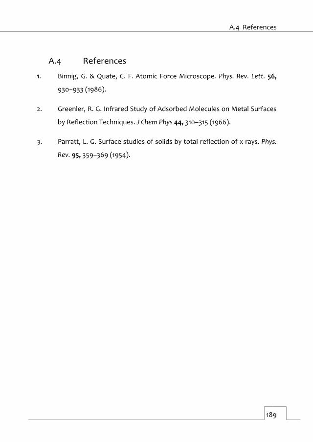
A.4 References
189
A.4 References
1. Binnig, G. & Quate, C. F. Atomic Force Microscope. Phys. Rev. Lett. 56,
930–933 (1986).
2. Greenler, R. G. Infrared Study of Adsorbed Molecules on Metal Surfaces
by Reflection Techniques. J Chem Phys 44, 310–315 (1966).
3. Parratt, L. G. Surface studies of solids by total reflection of x-rays. Phys.
Rev. 95, 359–369 (1954).

190

191
Resumen en castellano
El objetivo principal de esta tesis ha sido el estudio de la funcionalización de
superficies ferromagnéticas mediante la formación de monocapas moleculares
autoensambladas, (SAMs, self-assembled monolayers) con el fin de conseguir
procesos sencillos y fiables para la preparación de interfaces híbridas aplicables
en dispositivos de espintrónica molecular.
La investigación se ha centrado en la funcionalización de materiales
ferromagnéticos, concretamente el cobalto y la aleación de níquel:hierro
conocida como Permalloy. Las propiedades magnéticas y de polarización de
espín de estos metales ferromagnéticos se mantienen a temperatura ambiente,
lo que los hace muy interesantes para su aplicación práctica en dispositivos
reales. Sin embargo, estos materiales presentan el inconveniente de su fácil
oxidación en condiciones ambientales, que les hace desarrollar una capa de
óxido antiferromagnética que pasiva la superficie.
Este manuscrito se divide en: un capítulo de introducción, tres capítulos de
resultados, un apartado de conclusiones y perspectivas generales, una sección
que describe la metodología experimental desarrollada y empleada a lo largo
de la tesis y finalmente ,un apéndice de marco teórico de algunas técnicas de
caracterización.

Resumen en castellano
192
En el capítulo de introducción se presentan brevemente los conceptos usados
en el desarrollo de esta tesis: (1) descripción del concepto de SAM y su
estructura, (2) resumen de las técnicas de caracterización de superficies usadas
para estudiar las monocapas y (3) varias aplicaciones de las SAMs en diferentes
campos, con especial hincapié en el campo de la espintrónica molecular.
La SAM se forma a partir de la autoorganización de una molécula de
surfactante en una superficie por vía vapor o en disolución. Las moléculas que
forman la SAM se dividen en tres partes: (i) Grupo funcional que define la
afinidad a anclarse en determinado tipo de superficie, (ii) cuerpo o esqueleto
cuyas interacciones intermoleculares débiles ayudan a la correcta
autoorganización en la monocapa y (iii) grupo funcional terminal que definirá
las características de la nueva superficie como el carácter hidrófilo/hidrófobo
de la misma, o la carga superficial etc. Técnicas que se usan comúnmente para
su caracterización son: Medidas de ángulo de contacto, microscopía de fuerza
atómica (AFM), espectroscopia Raman, espectroscopia infrarroja por reflexión
(IRRAS), espectroscopia de electrones (Auger) o de rayos-X (XPS:
espectroscopia de fotoelectrones emitidos por rayos-X y XAS: espectroscopia
de absorción de rayos-X), reflexión y difracción de rayos-X (XRR y XRD
respectivamente) y la espectrometría de masas de desorción/ionización láser
asistida por matriz acoplada a un detector de tiempo de vuelo (MALDI-TOF).
La formación de SAMs se ha aplicado para control y modificación de la
hidrofobicidad de las superficies, como enganche para el anclaje de otras
especies a la superficie (con especial interés en el desarrollo de sensores o
detectores), como capa protectora incluso frente a tratamientos de ataque

Resumen en castellano
193
químico, y en electrónica molecular, participando como diferentes
componentes electrónicos de los sistemas. En el siglo XXI, las SAMs han
encontrado aplicación en el campo de la espintrónica molecular. La
espintrónica se basa en el uso no sólo de la carga del electrón sino también de
su espín, para almacenar y procesar información. La espintrónica molecular
incorpora el uso de los materiales orgánicos, ya que al estar compuestos por
elementos ligeros, como carbono, hidrógeno y oxígeno, tienen interacciones
hiperfinas y acoplamiento espín-orbita muy débiles, que promueven la alta
difusión del espín. Este factor es importante a la hora de sustituir por moléculas
los materiales tradicionales y óxidos inorgánicos, que se usan como barreras
para separar dos electrodos ferromagnéticos. Los primeros trabajos que
emplearon una SAM como espaciador, entre dos electrodos de níquel, o de
níquel y cobalto, se publicaron respectivamente por Petta en el 2004 y Wang en
el 2006. Ambos, detectaron el magnetorresistencia de efecto túnel (TMR) en
su geometría de unión túnel magnético (MTJ). Dicho efecto, es la base de
funcionamiento de las MTJ. Cuando se aplica una diferencia de potencial, se
genera una corriente polarizada que fluye desde el electrodo ferromagnético
inferior hasta el electrodo ferromagnético superior, que atraviesa el separador,
normalmente un material no magnético. La magnitud de la corriente depende
de la orientación de la magnetización de los electrodos. Aplicando un campo
magnético externo, es posible actuar singularmente sobre cada electrodo
ferromagnético, cambiando dicha orientación de paralela a anti paralela. Este
giro produce un aumento en la resistencia del tránsito de los electrones.
Resumiendo, dependiendo de la orientación relativa de los electrodos es
posible definir dos estados diferentes de resistencia eléctrica. Para garantizar el

Resumen en castellano
194
giro selectivo, se pueden usar diferentes materiales ferromagnéticos. El efecto
túnel se debe al carácter aislante del espaciador, y su grosor nanométrico. En
los ejemplos reportados en literatura, ambos autores han evidenciado estos
cambios de resistencia, desafortunadamente a la temperatura de 4 K. Otro
ejemplo más reciente, fue reportado por Galbiati et al., que usó un óxido de
lantano, manganeso y estroncio (LSMO) que posee una polarización de espín
del 100% a bajas temperaturas. Estos resultados tan prometedores dejan el
campo abierto a nuevas investigaciones hacia la incorporación de SAMs en
dispositivos espintrónicos que funcionen a temperatura ambiente, lo que
explica la motivación de esta tesis.
En el capítulo dos, hemos investigado la posibilidad de formar SAMs de cadenas
alquílicas utilizando la capa de óxido superficial que pasiva al permaloy ya que
en la literatura no se han encontrado protocolos para su funcionalización.
Elegimos como grupo de anclaje el ácido fosfónico que se usa tradicionalmente
para funcionalizar los óxidos de metales y trabajamos con ácidos
alquilfosfónicos de diferente longitud de cadena empezando por el ácido
dodecilfosfónico (C12P), hasta el ácido octadecilfosfónico (C18P). Recurrimos a
diferentes tratamientos con plasma como alternativa para limpiar y/o activar el
óxido, y observamos que tratando la superficie con un plasma suave de
hidrógeno, se produce un incremento en la cantidad de hidróxidos lo que
aumenta la reactividad. De hecho, al exponer una superficie pre-tratada con
hidrógeno, observamos una disminución de ángulo de contacto del agua,
respecto a las muestras expuestas solamente a disolvente. Tras las
funcionalización con las moléculas de alquilfosfónico, la superficie modificada
presenta un carácter hidrófobo, con ángulos mayores de 110o y el valor sigue

Resumen en castellano
195
una tendencia monótona al aumentar la longitud de la cadena de carbonos,
pasando de 110 o para un C12P hasta un 118 o para un C18P. Esta variación de
hidrofobicidad de la superficie, también fue empleada para estimar en cuánto
tiempo se forma una monocapa completa sobre este sustrato. El resultado fue
que, el crecimiento de la monocapa está formado por dos procesos
cooperativos, de duración total de 3 horas. La primera etapa es la aproximación
de las moléculas a la superficie y que tiene lugar en unos pocos segundos y la
segunda es la reorganización molecular, que dura unas decenas de minutos.
Todo el proceso de crecimiento se lleva a cabo siguiendo el modelo de
crecimiento uniforme, en el cual se forma un film de moléculas recostadas
sobre la superficie y a medida que el recubrimiento crece, las moléculas van
adquiriendo una inclinación uniforme, según su empaquetamiento hasta llegar
a la formación de una monocapa ordenada. Pudimos obtener información
sobre los ángulos de inclinación, respecto a la normal de la superficie, mediante
IRRAS, una técnica de caracterización sensible a las vibraciones
perpendiculares a la superficie de los grupos funcionales. Según se aumentaba
la longitud de la cadena, observamos un ángulo menor de inclinación,
relacionado con su grosor, que indicaría la transición desde un film menos
ordenado hacia uno más ordenado. Combinando este dato con la información
extraída por XRR, obtuvimos el grosor de la SAM formada, desde 1.5 nm en el
caso de C12P hasta 2.5 nm en el del C18P. Además, mediante el uso de la técnica
de XPS, identificamos la presencia de fósforo, relacionada con el grupo
fosfónico en la superficie y estudiando el cambio en las intensidades de los
picos de níquel y carbono, en función de la molécula usada, pudimos obtener
una tercera estimación del grosor molecular, confirmando los valores del XRR.

Resumen en castellano
196
Utilizamos la espectrometría de masas MALDI–TOF como técnica con
ionización suave que garantiza la ausencia de fragmentación del analito y nos
permitió demostrar la integridad de las moléculas en la superficie. Además, no
se detectaron picos relativos a la presencia de una multicapa, situados
teóricamente al doble del peso molecular más un átomo de hidrógeno. El C18P,
pudo ser estudiado por esta técnica debido a interferencias en el espectro con
la matriz usada para transferir electrones al analito. Las propiedades
magnéticas de las superficies funcionalizadas fueron detectadas por
espectroscopia magneto óptica del efecto Kerr (MOKE), que se basa en el
estudio de la variación en la polarización de un láser al incidir en la superficie
magnética, en presencia de un campo magnético externo. Es una técnica muy
sensible al magnetismo de superficies. El óxido de permaloy se ordena
antiferromagnéticamente a bajas temperaturas. El grueso del material, de
forma opuesta, tiene un comportamiento ferromagnético. La cercanía de un
material ferromagnético a otro antiferromagnético se refleja en un
ensanchamiento de la curva de histéresis magnética, debido al fenómeno de
interacción de canje. La histéresis magnética de una muestra funcionalizada
con la SAM de ácidos alquilfosfónicos es igual a una muestra sin funcionalizar,
oxidada al aire. Eso demuestra que la funcionalización no afecta a las
propiedades magnéticas del óxido y del grueso del material. Para comprobar la
calidad de nuestra SAM, se consiguió dibujar un patrón de líneas por medio de
un método de litografía suave, llamado impresión por microcontacto
(microcontact printing). Se embebió un sello de una resina polimérica, que
presenta un patrón de líneas, con una disolución de ácidos alquilfosfónico, y lo
pusimos en contacto con una superficie oxidada de permalloy, previamente

Resumen en castellano
197
tratada con plasma de hidrógeno. Debido al contacto directo entre la molécula
y la superficie a funcionalizar, la reacción tiene lugar en cuestión de segundos,
obteniendo la transferencia del patrón de líneas. Se estudió la topografía de la
superficie por AFM, en modo contacto, ya que, de otra manera no se podía
visualizar. Para poder revelar el patrón, se expuso la superficie a una disolución
de ácido glicólico, que ataca las zonas no funcionalizadas. El resultado final fue
un patrón de líneas, con resolución micrométrica, que demuestra la validez de
estas SAMs como barreras resistente a un ataque químico. Como conclusión
del capítulo 2 podemos destacar que, se ha llevado a cabo por primera vez la
funcionalización del óxido de permalloy, que no había sido reportada en
literatura. El punto crítico fue el pretratamiento de la superficie con un plasma
de hidrógeno suave, que promueve el incremento de grupos hidróxido en el
óxido original, favoreciendo la reacción de condensación con el grupo
fosfónico. Se ha logrado formar una SAM de ácidos alquilfosfónicos, compacta
y de tamaño nanométrico. Su robustez se ha comprobado con su uso como
agente resistente a un ataque químico y protector de la superficie de permaloy
subyacente.
En el capítulo tres pasamos al estudio de la funcionalización directa del material
ferromagnético (cobalto o permalloy). El objetivo fue recuperar metales
ferromagnéticos que ya han sido expuestos al aire y por tanto pasivados con
una capa de óxido antiferromagnético que representa una fuente de
despolarización del espín. El ataque del óxido permite que quede expuesto
directamente el material ferromagnético para reaccionar con la unidad
molecular que dará lugar a la formación de la SAM. Para la funcionalización de
metales como oro, plata y cobre, generalmente, se han empleado SAMs de

Resumen en castellano
198
alcanotioles. Se han reportado métodos variados de ataque del óxido que o
resultan caros u originan superficies rugosas, que no son compatibles con
trabajo en atmosfera inerte o con procesos litográficos y por tanto no son
óptimos para su aplicación en la fabricación de dispositivos espintrónicos.
Durante nuestra investigación se observó que al exponer una superficie
oxidada de cobalto o permaloy a una disolución etanólica de ácido glicólico, se
producía un ataque completo (etching) del material. Repitiendo el mismo
experimento en atmósfera inerte, el proceso se detenía una vez que había
alcanzado la superficie metálica, resultado en un ataque selectivo de la capa de
óxido. Por XPS se comprobó la ausencia de picos de oxígeno, que confirma una
recuperación del metal desnudo. Las propiedades magnéticas después del
tratamiento han revelado también que se han recuperado los campos
coercitivos de una muestra que no presenta óxido superficial. La
funcionalización con una SAM se llevó a cabo exponiendo las superficies a una
disolución de ácido glicólico en atmósfera inerte y tras transcurridos 15
minutos, se les añadió la disolución de alcanotioles deseada. El resultado, tras
pasar 16 horas de reacción, se detectó con un aumento de la hidrofobicidad de
la superficie, respecto a la superficie que fue expuesta sólo al ácido glicólico. Se
ha observado que, a medida que la cadena usada para funcionalizar la
superficie aumentaba de doce átomos de carbonos (C12S) a dieciocho (C18S), el
ángulo de contacto de agua pasaba de110o a 114 o. Continuando con la
caracterización, sin exponer la superficie funcionalizadas al aire, se ha
observado mediante medidas de absorción de rayos-X que la formación de la
SAM en la superficie tras la eliminación del óxido, no provocaba la re-oxidación
de esta..

Resumen en castellano
199
En colaboración con CNRS\Thales, se fabricaron MTJ de área nanométrica
mediante litografía láser, para disminuir la probabilidad de cortocircuitos. La
superficie del permalloy, se funcionalizó aplicando la metodología desarrollada
en este capítulo con una SAM de alcanotioles y se completó el dispositivo con
un electrodo superior de cobalto. Se pudo detectar un efecto de TMR del 16% a
temperatura ambiente, en un dispositivo que empleaba una monocapa de
C16S.
Resumiendo, la exposición, en atmósfera inerte de un sustrato oxidado de
cobalto o permaloy a una disolución de ácido glicólico, permite el ataque
selectivo del óxido antiferromagnético, sin afectar las propiedades magnéticas
del grueso del material y además permite su funcionalización con una SAM de
alcanotioles que puede integrarse en dispositivos espintrónicos. Finalmente
hay que destacar que se observó un comportamiento anómalo una vez los
sustratos funcionalizados con alcanotioles eran expuestos al aire, ya que se
detectó por microscopia óptica el crecimiento espontáneo de dominios
laminares en la superficie.
En el capítulo 4 describimos el estudio para identificar la naturaleza de estos
dominios laminares, que aparecen exclusivamente, en las superficies metálicas
ferromagnéticas funcionalizadas con SAM y expuestas al aire, de manera
espontánea, sin ningún tipo de estímulo externo. La primera hipótesis que
descartamos fue que estaban compuestos por óxidos inorgánicos, ya que se
encontró una dependencia lineal de la altura de escalón que se define de forma
repetitiva en estos dominios, con la longitud de cadena de la molécula usada
para funcionalizar la superficie; a medida que la longitud de la molécula

Resumen en castellano
200
aumenta, observamos que la altura de escalón también aumentaba desde 3.6
nm hasta 4.6 nm, al pasar de un C14S a un C18S, respectivamente. Este
resultado fue confirmado también por medidas de XRD que evidenciaron la
dependencia con la molécula usada para funcionalizar la superficie, sobre todo
por la correlación linear que es una clara señal de que estos dominios
comparten la misma estructura interna. En base a estos estudios de AFM y
XRD, y en la existencia de estructuras conocidas crecidas en polvo de
materiales laminares de alcanotioles que coordinan cationes metálicos según la
fórmula RS-M-SR, intentamos hacer un modelo que describiera la estructura de
los dominios observados, sin embargo este es sólo una aproximación debido al
error experimental en las medidas de AFM y de XRD.
Por AFM también, ha sido posible determinar la altura media por material
(cobalto o permaloy) y por cadena empleada, observando que con C14S se
obtienen islas más altas, hasta unas 10 capas, y con C18S se obtienen islas más
finas, de una capa. Este resultado se mantiene también pasando de cobalto a
permalloy. Por medio de microscopia óptica, se ha estudiado el área media de
las islas, pudiendo abarcar superficies amplias en cuestión de minutos, en lugar
de recurrir al AFM, para una medida más exacta, pero que requiere mayor
tiempo y por tanto menor superficie analizada. Se ha observado que utilizando
la cadena más corta C14S, se obtiene una baja densidad de islas, pero con
mucha variedad de tamaños, por encima de las 90 micras cuadradas. Sin
embargo, con la molécula más larga C18S, se obtiene una alta densidad de islas,
pero de tamaño inferior a las 20 micras cuadradas. La densidad obtenida se
refleja en el recubrimiento de la superficie, siendo eso alrededor de un 6% para
el C14S y un 24% para el C18S. Mediante el estudio de la altura media obtenida

Resumen en castellano
201
por AFM, y del área media, obtenida por microscopía óptica, se pueden hacer
estimaciones rápidas, sobre qué cantidad de material, que originariamente
formaba parte de la SAM en la superficie, y después se ha reorganizado en los
dominios laminares. Según los cálculos, siempre queda parte de las moléculas
en la superficie ocupando el espacio entre los dominios, siento en el caso de
moléculas más largas (C18S) cuando mayor proporción de moléculas migran
hacia los dominios. También se ha evidenciado desde los histogramas de altura,
que existe un fenómeno de interdigitación entre los dominios formados con la
monocapa subyacente en el caso del C18S. En el caso de C16S y C14S, no se ha
relevado este tipo de interacción entre la monocapa y los dominios.
Las medidas hechas por espectroscopia Raman y Auger con carácter local, han
servido para confirmar nuestro primer modelo de composición de los dominos
laminares, mediante su potente resolución espacial. La espectroscopia Raman,
ha sido útil para localizar y medir las vibraciones pertenecientes a las cadenas
alquílicas en los dominios laminares. Por otro lado, la espectroscopia Auger, ha
confirmado la presencia de iones cobalto y de azufre en el interior de las islas,
desafortunadamente no se logrado estimar su estado de oxidación, debido a
las limitaciones de la técnica. Los resultados confirman nuestra idea preliminar
de una estructura tipo sandwich, donde las cadenas alquílicas se extienden por
arriba o por debajo de una capa de iones metálicos a los que coordinan por el
azufre.
Así mismo también ha sido posible seguir la aparición y evolución de los
dominios al entrar en contacto la muestra con el aire, por medio de AFM y de
microscopía óptica. Cabe resaltar que estos dominios laminares, tienen no sólo
Resumen en castellano
202
una etapa de crecimiento en vertical, sino también en lateral, sufriendo
también etapas de coalescencia, cuando dos o más dominios se encuentran,
para fundirse en uno de tamaño mayor. Se ha detectado que la evolución en
área y altura dura aproximadamente 16 horas hasta llegar a una situación
estable. Para probar que efectivamente los dominios sólo aparecían al contacto
con el aire, se realizaron medidas de AFM de muestras que nunca habían sido
extraídas de la caja seca tras la funcionalización, gracias al equipamiento
disponible en los laboratorios de CNRS\Thales en el grupo del profesor P.
Seneor. Allí existe un AFM dentro de la caja seca donde se realiza el
tratamiento con ácido glicólico y posterior crecimiento de la SAM, lo que
permite la adquisición de la imagen previa a la exposición al aire, sin embargo,
la calidad de las imágenes se ve comprometida por las vibraciones de la caja.
Para comprobar el papel que juegan la temperatura y la humedad en el
crecimiento espontáneo de los dominios laminares se realizaron dos tipos de
experimento diferentes, en el primero se prepararon diferentes muestras de
monocapas sobre cobalto en caja seca y al sacarlas unas se introdujeron en el
nevera a 5oC, otras se dejaron a temperatura ambiente y otras se colocaron
sobre una placa calefactora a 35oC, la muestras se inspeccionaron por
microscopía óptica tras 23 horas y se observó que las islas habían crecido en
todos los substratos, pero que en las muestras a menor temperatura el número
de islas era mucho mayor pero estas eran de tamaño mucho más pequeño,
mientras que las muestras a alta temperatura el número de islas era menor
pero estas tenían una tamaño mucho mayor en área y altura, este
comportamiento se asemeja a la cristalización de sistemas en disolución ya que
la falta de energía térmica dificulta la migración de las moléculas. Para estudiar

Resumen en castellano
203
la influencia de la humedad se prepararon muestras de monocapas en cobalto
en la caja seca que al extraerse se expusieron una a la atmósfera normal del
laboratorio y otra dentro de un dispositivo con un flujo de aire seco. Tras 16
horas se estudiaron las muestras por microscopía óptica (al ambiente) y se
observó que en ausencia de humedad las islas también habían aparecido sin
diferencias de tamaño o número muy significativas aunque siempre inferiores
que en el caso de la muestra en aire seco. Ambos tipos de muestra se dejaron
expuestas al ambiente del laboratorio y tras 16 horas más se vio que la muestra
que habían estado expuesta al aire húmedo ambiental desde el principio no
sufría ninguna evolución mientras que la que había estado en aire seco durante
las primeras horas seguía evolucionando en tamaño y número hasta alcanzar
una estadística similar a la otra muestra. Este estudio parece indicar que
aunque la humedad no es determinante para la aparición de los dominios
laminares, sí que determina su velocidad de crecimiento.
Por otro lado, hemos observado que, si se toman imágenes consecutivas con el
AFM sobre uno de estos dominios, se produce un fenómeno raro e
impresionante a la vez, donde a medida que el número de imágenes aumentan,
el área y altura de la misma van disminuyendo de manera notable y de forma
discreta (capa a capa). De hecho, el efecto que se nota es que el material
desaparece al pasar la punta del AFM, que está midiendo en modo tapping, es
decir, en contacto intermitente entre la punta y la superficie y no arrastra el
material. Esto puede significar que el material: 1) no está enlazado
covalentemente con la superficie, 2) no tiene mucha interacción entre capas,
que conlleva al punto 3) que es un material que se puede delaminar en
superficie. Un aspecto importante, es que en las zonas donde se ha quitado el

Resumen en castellano
204
material, no se evidencia la presencia de un agujero en la superficie, que
significa que la SAM subyacente a la isla tiene una conformación homogénea.
A la vista de los resultados obtenidos, proponemos un mecanismo de
formación de los dominios laminares basado en el idea de que la SAM se forma
en condiciones de atmósfera inerte de forma normal, pero una vez expuesta al
aire, el oxígeno encuentra unos defectos para empezar a reaccionar oxidando
la superficie metálica y una vez oxidados algunos centros metálicos, se produce
una migración de estos iones coordinados por los tioles fuera de la superficie
por encima de la SAM, obligando a que las otras moléculas que forman parte de
la monocapa se reorganicen. El proceso sigue hasta que todos los iones
metálicos se oxidan y que la monocapa disminuye drásticamente su densidad.
Después de nuestro estudio exhaustivo sobre la funcionalización molecular de
los metales ferromagnéticos y las conclusiones principales extraídas, surgen
nuestras perspectivas que investigar. La formación de SAMs sobre la capa
pasivante de óxido sin afectar el metal subyacente y compactas y homogéneas
que pueden nanoestructurarse por litografía suave y pueden usarse de agente
protector frente a ataque químico nos lleva a intentar dibujar estructuras más
complejas de permaloy propias de circuitos, que pueden aprovecharse en la
preparación por ejemplo de nanosensores. La preparación de las SAMs
directamente sobre el material ferromagnético recuperado nos ha motivado a
trabajar a la implementación de esa metodología para la formación de SAMs
más complejas, por ejemplo como constituidas por radicales orgánicos, que
pueden ser de interés especial como interfaces en dispositivos espintrónicos.
En referencia a la formación espontánea de dominios cuando las superficies

Resumen en castellano
205
funcionalizadas son expuestas al aire, todavía, quedan unas cuestiones abiertas
que se tendrán que investigar con más detalle. Por ejemplo, sobre el
mecanismo que está involucrado en la formación de esas islas, el tipo de
coordinación de los iones metálicos, o si es posible de evitar la formación de
esas islas preparando SAMs interconectadas que pudieran prevenir la oxidación
de la superficie. Además, queremos estudiar si el uso de una superficie
metálica, en lugar de una superficie recuperada, juega un papel importante en
la aparición y crecimiento de las islas.

206