Gain Theory And Models In Silicon Nanostructures
20
GAIN THEORY AND MODELS IN SILICON NANOSTRUCTURES Paper dedicated to the memory of Claudio Bertarini STEFANO OSSICINI a , C. ARCANGELI b , O. BISI a , ELENA DEGOLI a , MARCELLO LUPPI b , RITA MAGRI b , L. DAL NEGRO c , L. PAVESI c a INFM-S3 and Dipartimento di Scienze e Metodi dell’Ingegneria, Università di Modena e Reggio Emilia; b INFM-S3 and Dipartimento di Fisica, Università di Modena e Reggio Emilia; c INFM and Dipartimento di Fisica, Università di Trento 1. Introduction The main goal in the information technology is to have the possibility of integrating low-dimensional structures showing appropriate optoelectronic properties with the well established and highly advanced silicon microelectronics present technology [1,2,3,4]. Therefore, after the initial impulse given by the work of Canham on visible lumines- cence from porous Si [5], nanostructured Si has received extensive attention both from experimental and theoretical point of view during the last ten years (for review see Refs. [6,7,8,9,10,11,12]). This activity is mainly centered on the possibility of getting relevant optoelectronic properties from nanocrystalline Si, which in the bulk crystalline form is an indirect band gap semiconductor, with very inefficient light emission in the infrared. Although some controversial interpretations of the visible light emission from low-dimensional Si structures still exist, it is generally accepted that the quantum con- finement, caused by the restricted size, and the surface passivation are essential for this phenomenon [12]. Here we will review our activity in the field of the theoretical determination of the structural, electronic and optical properties of Si nanocrystals (Si-nc). The present work aims at answer a very important question related to the origin of the enhanced photoluminescence in Si-nc embedded in SiO 2 . In fact, optical gain has been recently observed in ion implanted Si-nc [13] and in Si-nc formed by plasma enhanced chemical vapor deposition and annealing treatments [14]. We propose, here, an analysis of the experimental findings based on an effective rate equation model for a four level system; moreover looking at our theoretical results for the optical properties of Si-nc we search for structural model that can be linked to the four level scheme. As final outcome, due to the results for the optoelectronic properties of Si-nc in different interface bond con- figurations, we demonstrate that in order to account for the striking photoluminescence properties of Si-nc it is necessary to take carefully into account not only the role of quantum confinement, but also the role of the interface region surrounding the Si-nc. We’ll firstly give a description of the rate equation model we have used and of the ob- tained results (section 2). After an introduction of the different theoretical methods (sec- tion 3) used in our calculations, we’ll describe our results on the electronic and optical
-
Upload
independent -
Category
Documents
-
view
1 -
download
0
Transcript of Gain Theory And Models In Silicon Nanostructures

GAIN THEORY AND MODELS IN SILICON NANOSTRUCTURES Paper dedicated to the memory of Claudio Bertarini
STEFANO OSSICINIa, C. ARCANGELIb, O. BISIa, ELENA DEGOLIa, MARCELLO LUPPIb, RITA MAGRIb, L. DAL NEGROc, L. PAVESIc a INFM-S3 and Dipartimento di Scienze e Metodi dell’Ingegneria, Università di Modena e Reggio Emilia; b INFM-S3 and Dipartimento di Fisica, Università di Modena e Reggio Emilia; c INFM and Dipartimento di Fisica, Università di Trento
1. Introduction The main goal in the information technology is to have the possibility of integrating low-dimensional structures showing appropriate optoelectronic properties with the well established and highly advanced silicon microelectronics present technology [1,2,3,4]. Therefore, after the initial impulse given by the work of Canham on visible lumines-cence from porous Si [5], nanostructured Si has received extensive attention both from experimental and theoretical point of view during the last ten years (for review see Refs. [6,7,8,9,10,11,12]). This activity is mainly centered on the possibility of getting relevant optoelectronic properties from nanocrystalline Si, which in the bulk crystalline form is an indirect band gap semiconductor, with very inefficient light emission in the infrared. Although some controversial interpretations of the visible light emission from low-dimensional Si structures still exist, it is generally accepted that the quantum con-finement, caused by the restricted size, and the surface passivation are essential for this phenomenon [12].
Here we will review our activity in the field of the theoretical determination of the structural, electronic and optical properties of Si nanocrystals (Si-nc). The present work aims at answer a very important question related to the origin of the enhanced photoluminescence in Si-nc embedded in SiO2. In fact, optical gain has been recently observed in ion implanted Si-nc [13] and in Si-nc formed by plasma enhanced chemical vapor deposition and annealing treatments [14]. We propose, here, an analysis of the experimental findings based on an effective rate equation model for a four level system; moreover looking at our theoretical results for the optical properties of Si-nc we search for structural model that can be linked to the four level scheme. As final outcome, due to the results for the optoelectronic properties of Si-nc in different interface bond con-figurations, we demonstrate that in order to account for the striking photoluminescence properties of Si-nc it is necessary to take carefully into account not only the role of quantum confinement, but also the role of the interface region surrounding the Si-nc. We’ll firstly give a description of the rate equation model we have used and of the ob-tained results (section 2). After an introduction of the different theoretical methods (sec-tion 3) used in our calculations, we’ll describe our results on the electronic and optical
Administrator
to be published in Towards the first silicon laser edited by L. Pavesi, S. Gaponenko, L. Dal Negro, NATO Science Series (Kluwer Academic Publishers, Dordrecht 2003)

properties of Si-nc in their ground and excited states and we will link these results to the model used for the rate equations. In section 5 we’ll be concerned, instead, with the de-termination of the optimized geometry for Si nanodots and clusters; in particular, we will investigate the role of oxidation processes at the surface of the Si-nc. Section 6 will be devoted to the description, including preliminary results, of our ab-initio gain calcu-lation for Si-nc. Finally section 7 will be devoted to the development of a model for the calculation of the optoelectronic properties of Si-nc embedded in a SiO2 matrix. 2. The four level scheme and the rate equation model Although a full theoretical calculation of the stimulated emission processes in Si-nc is still lacking due to the formidable difficulties, a rather simplified phenomenological ap-proach is possible. On the basis of the experimental findings we propose a rate equation model to explain the major features of the gain experiments [13,14]: i) the almost com-plete absence of optical absorption at the peak gain emission for all the amplifying Si-nc samples; ii) a moderate low pumping threshold of about 0.5 kW/cm2 for population in-version. Items i) and ii) can be explained within an effective four-level model. The cor-responding set of rate equations for photons and carriers includes both amplified stimu-lated emission and Auger recombination. In particular, we assume that levels 2-4 are empty before the excitation occurs. Once the pumping starts, levels begin to be popu-lated and two different Auger non-radiative recombination processes can in principle take place. The first consists in an electron relaxation from energy level 3 to level 2 with the energy given to a second electron which is also present in the same level 3 and which is promoted to higher lying levels in the conduction band, from which a very fast relaxation to level 4 occurs. This Auger process involves two electrons in the same level, and therefore the rate of the process depends quadratically through a coefficient CA1 on the level population N3. Another Auger mechanism involving an electron in the level 3 and a free hole in the valence band edge (level 1) can in principle occur, where the hole is sent deep in the valence band and then very rapidly relaxes again to the band edge. This process has to be proportional, through a coefficient CA2, to the product of the population of the emitting level 3 (N3) and the hole concentration in the valence band edge (Nh). Nh equals the total concentration of electrons in the various excited lev-els, that is Nh= N2+N3+N4 . Within the four level scheme we are proposing, the relaxa-tion times of electrons from levels 4 and level 2 are so fast that N4 and N2 are always almost empty. Therefore Nh ≈ N3. Hence, the following set of coupled rate equation has to be integrated, where Ni represent the level population densities (i=1,..,4), σP is the ab-sorption cross section at the wavelength of the pump, φP is the time dependent pumping photon flux, Γij are the relaxation rates from the i to the j energy levels, τ is the total lifetime of the emitting level N3, B is the stimulated transition rate which implicitly con-tains the gain cross section σ, nph is the emitted photons number, Va is the optical mode volume, τph is the photon lifetime, β is the spontaneous emission factor and τR is the ra-diative lifetime of N3. CA is an effective Auger coefficient equal to 2CA1 +CA2, taking into account both of the two particles Auger processes (e-e or e-h):

Rph
phpha
ph
PPA
Aph
AAph
PP
NnNNBnV
dtdn
NNtNCdt
dN
NCNNNBnNdt
dN
NCCNNBnNNdt
dN
NNtdt
dN
τβ
τ
φσ
τ
τ
φσ
323
44312
314
2344323
33
232123221
32
22111
)(
)(
)(
)()(
)(
+−−=
Γ−+=
−Γ+−−−=
++−+Γ−=
Γ+−=
(1)
It is possible to observe optical gain whenever the stimulated emission rate is greater than the Auger recombination rate. From Eq. (1) it is possible to define a SE lifetime as:
31 4 13se nc
ph ph
RBn cn
τ πξσ
= = (2)
where ξ isthe Si-nc volume fraction and cBV
σ= , valid under the assumption of
monochromatic incident light, is used.
0 5 0 1 0 0 1 5 0
1
4 2 % S i , T A = 1 2 5 0 ° C
P.L
.In
ten
sit
y (
a.u
.)
T i m e ( n s )
Figure 1. (symbols) RT time resolved decay curve [14]. Detection wavelength was 750 nm. (full line) Emitted photon numbers obtained by solving the four levels model with an Auger lifetime of 20 ns, a gain cross sec-tion of 1.2x10⁻¹⁷ cm2, a nc density of 6x1018 cm-3 and a pumping photon flux of 1018 photons/(s cm2). (dashed line) Emitted photon numbers obtained by solving the four levels model with the same parameters and ne-glecting stimulated emission. All the curves are normalized to unity.

An equivalent Auger recombination time can be defined as follows:
3
12A
AC Nτ = (3)
It is clear that to observe gain 1/τse ≥ 1/τA or equivalently, if we define a competition fac-tor A seC τ τ= , C ≥1. This poses a condition on the volume fraction. The proposed rate equation model fits qualitatively the experimental data. Fig. 1 shows an example. 3. Methods of calculations of the structural, electronic and optical properties For the calculations of the structural and optoelectronic properties of Si-nc both in their ground and excited states (section 4) we adopt the Hartree-Fock scheme within the Ne-glect of Differential Overlap (NDO) approximation, using the MNDO-AM1 scheme for geometries and INDO for optical spectra [15]. In the excited state one electron is taken from the highest occupied molecular orbital (HOMO) (hole in the valence) and placed in the lowest unoccupied molecular orbital (LUMO) (electron in the conduction), also here the geometry is optimised and the optical properties are calculated fully taking into account the excitonic coupling [16,17]. For what concerns the calculations on silicon nanoclusters (section 5) the theoretical basis has been the Density Functional Theory in the Local Density Approximation (DFT-LDA) [18] with a norm-conserving pseudopo-tentials approach to treat the electron-ion interaction. Pseudopotentials in the Kleinman and Bylander factorized form [19] for Si, H and O have been generated. We have per-formed total energy calculations through the FHI98md code [20]. All the atoms have been allowed to relax, until the residual forces have been less than 0.05 eV/Å. In order to simulate isolated (non-interacting) clusters with a three dimensional periodic bound-ary conditions method, we have considered a cubic supercell with a large side length. The optoelectronic properties of the relaxed systems have been obtained by a similar codes using ultrasoft pseudopotential [21]. For details see Ref. 22-23. Our total energy calculations on Si nanodots in SiO2 matrix (section 7) have been based on the CASTEP code [24]. The theoretical basis is the DFT in the gradient-corrected LDA version (GGA) [25,26]. The geometry optimization with the cell optimization has been per-formed using the BFGS scheme [27]. For the band structure calculations at relaxed ge-ometry, we have used the same acknowledgements as for the geometry optimization run but with a “band by band” electronic minimization method and 29 special k-points. For the optical properties the calculations has been performed with a LDA approach and not GGA, increasing the number of the k-points and including 44 empty states. Only direct (same k-point) inter-band (VB-CB) transitions have been taken into account [22,23] 4. Si-nc in their ground and excited states: a four level system Here we describe the investigation of the structural and electronic properties of small hydrogenated nanoparticles, including the effect of incorporation of a Si=O silanone unit: the investigation was conducted through Hartree-Fock techniques [16,17].

For Si-H nc we found that the absorption gap, in the stable relaxed ground state geometry, shows a strong blue shift with respect to the bulk Si that is due to both con-finement and relaxations effects. Fig 2 (a) shows the case of the Si44H42 cluster [16].
Figure 2. Optical spectrum calculated for the Si44H42 cluster in its (a) ground and (b) excited state configura-ton, corresponding to absorption and emission spectra respectively.
We then examine the optical properties of the same cluster in their excited state. With the geometry optimized for this electronic excited state, we again study the optical properties. Fig. 2 (b) shows the result. The difference is striking: the first transi-tion is drastically red shifted. This spectrum is more properly associated with photolu-minescence, whereas Fig. 2 (a) should correspond to absorption only. The origin of the red shift is related to the relaxation of the particle to a locally distorted equilibrium con-figuration.
What we find in fact is that the particle in the excited state undergoes a strong symmetry-lowering spontaneous distortion, extremely localized on two neighboring sur-face Si atoms, each bonded just to one H atom. In the distortion the Si atoms bend and stretch their bond, keeping the distance to their internal neighbors almost unchanged. One of the H atom moves to bridge the bond, so that a surface configurational defect is created, with no complete rupture of any bonds in the particle (see Fig. 3).
A similar effect is found for the case of the insertion of a oxygen double bonded (DoB) to a Si atom at the surface substituting two H atoms. Incorporation of such a Si=O unit perturbs both absorption and emission properties. The absorption is red shifted with respect to the Si-H corresponding case and the emission is another time strongly lowered with respect to the absorption (see Fig. 4). These results are due to the fact that the presence of the Si=O bond promotes in the ground state a slight distortion of the Si-Si backbonds, distortion that in the excited states is enhanced, together with the shortening of the Si=O bond length [17].
Similar results have been obtained by Filonov and coworkers [28] also for py-ramidal Si nanocluster as witnessed by Fig. 5, where the optimized cluster structures for both ground and excited state configurations for a Si30OH38 cluster are shown.

Figure 3. Atomic arrangement calculated for the Si44H42 cluster, in the ground (left) and in the excited (right) state. Shown are the six fold rings of Si atoms that involve the locally distorted bond and reach the center of the cluster.
Figure 4. Optical spectra for the Si35OH34 particles obtained by the substitution of a SiH2 unit with a Si=O double bond. (a) absorption spectrum, (b) emission spectrum, both calculated in their relaxed geometry.
Also in this case the calculation scheme used was a Hartee-Fock one. Once
more we see that the Si atoms that underwent the maximum shift from their ground state positions are the Si atoms in the vicinity of the double bonded O atom.
It is important to underline that the difference between the absorption and emission spectra are , in all cases, due to the very different spatial localization of the

HOMO and LUMO states. As showed in Fig. 6 for the case of the Si44H42 cluster, on going from absorption to emission, the HOMO state, previously localized on the inter-nal shell of Si atoms, is now strongly localized on the external Si atoms involved in the distortion. The same happens for the LUMO+1 state, this state is also partially involved in the lowest transition [16]. The structural distortion originates strongly localized states
Figure 5. Si30OH38 cluster structure for the ground (a) and excited (b) states. The Si atoms underwent the maximum shift from their equilibrium ground state positions are marked in black. Arrows indicate the Si=O bonds.
The picture that emerges is that of a four level scheme (previously proposed in
section 2), where level 1 and 4 are the HOMO amd LUMO levels of the ground state and the levels 2 and 3 are , instead the HOMO and LUMO levels of the excited states.

Figure 6. Spatial localization of single particle states in the Si44H42 cluster. Parts (a) to (c) refer to the absorp-tion and (d) to (f) to emission. The probability density associated with a typical atom in a given shell is plotted vs. its distance from the center of the cluster.
Figure 7. Energy levels (k-point Γ) for all the considered clusters at relaxed geometry: a) Si14H20 , b) Si14H16O2 , c) Si14H20O2 , d) Si12H16O2 .

5. Electronic and optical properties of Si nanoclusters: role of surface termi-nation and of multiple oxidation To better understand the role of surface termination and of multiple oxidation on the structural and optoelectronic properties of small silicon crystalline clusters, we have looked at the differences between similar systems with different types of Si-H and Si-O bonds [22,23]. We have built up a small cluster of 14 silicon atoms (3.7 x 5.7 x 6.7 Å) with a crystalline Td-interstitial structure and we have recovered it with hydrogen atoms in order to passivate all the dangling bonds (Si14H20 cluster). Then we have substituted some Si-H or Si-Si bonds with Si-O bonds. We have mainly focused our attention on three Si-O bond configurations: in Si14H16O2 cluster we have obtained two Si=O double bonds (DB), deleting four Si-H bonds on two Si atoms of the structure; in Si14H20O2 we have formed two Si-O-Si bridges breaking two Si-Si bonds in the crystalline skeleton; and in Si12H16O2 we obtained two Si-O-Si bridges substituting two Si atoms of the sili-con structure with O. All the clusters structures have been relaxed through geometry op-timization runs.
As expected, the H passivation has left the crystalline Si skeleton unchanged. In the case of Si=O DoBs (Si14H16O2), the changes are limited practically only to the Si-Si-Si bond angle under the Si=O bond (that is aligned along the (001) direction), and to the correspondent Si-Si bond lengths that are only a little strained. Concerning the Si14H20O2 and Si12H16O2 clusters there is an appreciable modification of the Si structure near the Si-O-Si bridges, with huge angles variations, but still with a small effect on the bond length.
In Fig. 7 the energy levels at k-point Γ for all the clusters are plotted. The com-parison between the hydrogenated case and the Si=O DoB shows a huge reduction of the energy gap (Eg) which goes respectively from 4.09 eV to 2.31 eV.
This reduction is due to the birth of new interface-related states which strongly modify the band edges. Looking at the energy levels for the two Si-O-Si bridges cases, it’s evident how the Si-O interface affects less strongly their behaviour. For the Si14H20O2 we register a very small Eg reduction, only 0.13 eV, while for Si12H16O2 the variation is more evident: Eg=3.61 eV, but less than for the Si=O DoB. It is important to remember that all these values are affected by the underestimation due to the LDA ap-proach (the scissor operator value for these confined systems can be evaluated around 0.8-1 eV). The analysis of the distribution of HOMO (highest occupied Kohn-Sham or-bital) and LUMO (lowest unoccupied Kohn-Sham orbital) helps to clarify the situation. In Fig. 8 are reported the isosurfaces at fixed value for the HOMO and LUMO of all the clusters. Only in the Si=O DoB case both HOMO and LUMO are localized around the oxygen of the Si-O bonds, while for the two cases with Si-O-Si bridges only part of the LUMO is around it; the HOMO actually maintains mainly the character of the hydro-genated structure, located along peculiar Si-Si bonds of the silicon skeleton.
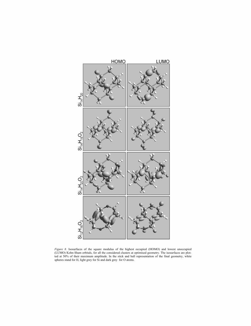
Figure 8. Isosurfaces of the square modulus of the highest occupied (HOMO) and lowest unoccupied (LUMO) Kohn-Sham orbitals, for all the considered clusters at optimised geometry. The isosurfaces are plot-ted at 50% of their maximum amplitude. In the stick and ball representation of the final geometry, white spheres stand for H, light grey for Si and dark grey for O atoms.

Figure 9. Absorption spectra (direct inter-band transitions) for all the considered clusters (relaxed geometry): a) Si14H20 , b) Si14H16O2 , C) Si14H20O2 , d) Si12H16O2 .The vertical lines indicate the calculated Eg.
This suggest that, in presence of Si=O DoB, the band edges are dominated by the surface states related to Si-O bonds and so the first transitions in an absorption proc-ess involves only the Si-O interface states; while for the Si-O-Si bridges the occupied states are still mainly related to the internal states along Si-Si bond directions, so that the character of the first optical transitions is still influenced by the crystalline silicon structure.
The optical properties reflect what we have observed for the electronic ones. In Fig. 9 we have reported absorption spectra for all the clusters. New features at the gap onsets characterize the absorption line-shapes. In the Si=O DoB case the first transitions have a very low probability: only a very tiny peak (highlighted by circle in Fig. 9b)) is present at energies around Eg. Also the Si12H16O2 presents a similar behaviour. These results go in the same direction of what reported by Vasiliev et al. [29] concerning the prohibition of the direct dipole transitions between HOMO and LUMO. At the same time the red shift in the absorption onset of these last two cases (respect to hydrogenated

one) compares well with the red shift observed in photoluminescence from high poros-ity porous Si samples after O exposition [30] and the experimental results for the band gap behaviour of heavily oxidized Si nanoparticles [31].
Figure 10. Calculated energy levels at the Γ point and total density of states (T-DOS) for the Si14Hn=Om clus-ters. In the y-axis are the energies calculated in eV. The alignment has been done simply equating the top of the valence bands in the different calculations.
To better simulate the progressive exposure to air of the porous Si samples we
have varied systematically the number of DoBs at the clusters surface and also the di-mension of the cluster itself (Si10Hn=Om, Si14Hn=Om). A non linear reduction of the en-ergy gap (Eg) with the DoBs number is shown, for all the cluster sizes. Each DoBs acts independently from the others causing the formation of localized states at the band edges. These findings provide a consistent interpretation of the experimental red shift behaviour in oxidized porous Si samples [30] and of recent results on the photolumines-cence peak bandwidth of single silicon quantum dots [32].
Figure 11. Electronic energy gap as a function of the number of Si=O double bonds at the cluster surface. Circle: Si10Hn=Om, square: Si14Hn=Om. The zero values correspond to the fully-H case for each cluser types.

The energy levels and total density of states (T-DOS) for the Si14Hn=Om clus-ters are reported in Fig. 10. The results confirm that in presence of DoBs the HOMO-LUMO transitions are allowed, even if not always very probable. The insertion of a sin-gle DoB at the surface produces a strong gap red shift which diminishes by increasing the NDs size (Si atoms number). New localized states related to the DoB appear within the gap at both bands. Their relative positions seem not to be strongly affected by size differences. The gap values are in fact held within 0.2 eV. Increasing the oxygen coverage level, i.e. adding new DoBs, the gap tends to decrease. The reduction however is not linear with the number of DoBs.
For all the cluster sizes, in fact, the strongest red shift is achieved with the first DoB; a second DoB produces a further reduction but weaker than the first and the more we add DoBs the more their contributions is smaller. Thus a sort of saturation limit seems to be reached. The plot of the electronic energy gap vs. the DoBs number (Fig. 11) shows clearly this behavior. A bigger number of DoBs at the surface can be seen as a longer exposure to air, i.e. oxidation, of the porous Si samples. Assuming that the ex-cited state doesn’t change radically the ground state band edges situation, our results reproduce perfectly the observed porous Si photoluminescence red shift behaviour for intentionally oxidized samples [30]. 6. “Ab-initio” calculation of gain For the wave intensity inside a medium we have I(z) =I0eγ(ω)z. Therefore γ(ω)<0 means absorption, γ(ω)>0 gain. γ(ω) is directly proportional to the imaginary part of the di-electric function through γ(ω)= - [ω/n(ω)c]ε2(ω), where n is the refraction index, thus it is possible to calculate the coefficient γ(ω) through ε2(ω). In the single particle approach and in the dipole approximation one has:
Where fm and fn are the quasi-Fermi level occupation probabilities. In the ground state is fm = 1 and fn = 0, thus we have always γ(ω)<0 and only absorption. In order to have gain some higher lying level must have an higher fn than some lower lying level (population inversion). Thus in order to calculate gain we must have a model for population inver-sion and we must calculate ε2(ω).
This has been done in the case of GaAs bulk. We started from our calculated eingenvalues/eigenstates through pseudopotential method. The positions of the quasi Fermi levels are determined from the calculated density of states
N =∫ ρ(E) fn(E,Fn) dE Where N is the number of electron/holes created in the systems.
ε ω πω
δ ε ω2
2
2 2
28( ) ( ) ( ( ) ), ,,
= − −∑∑em V
P k k f fm n m n m nkm n
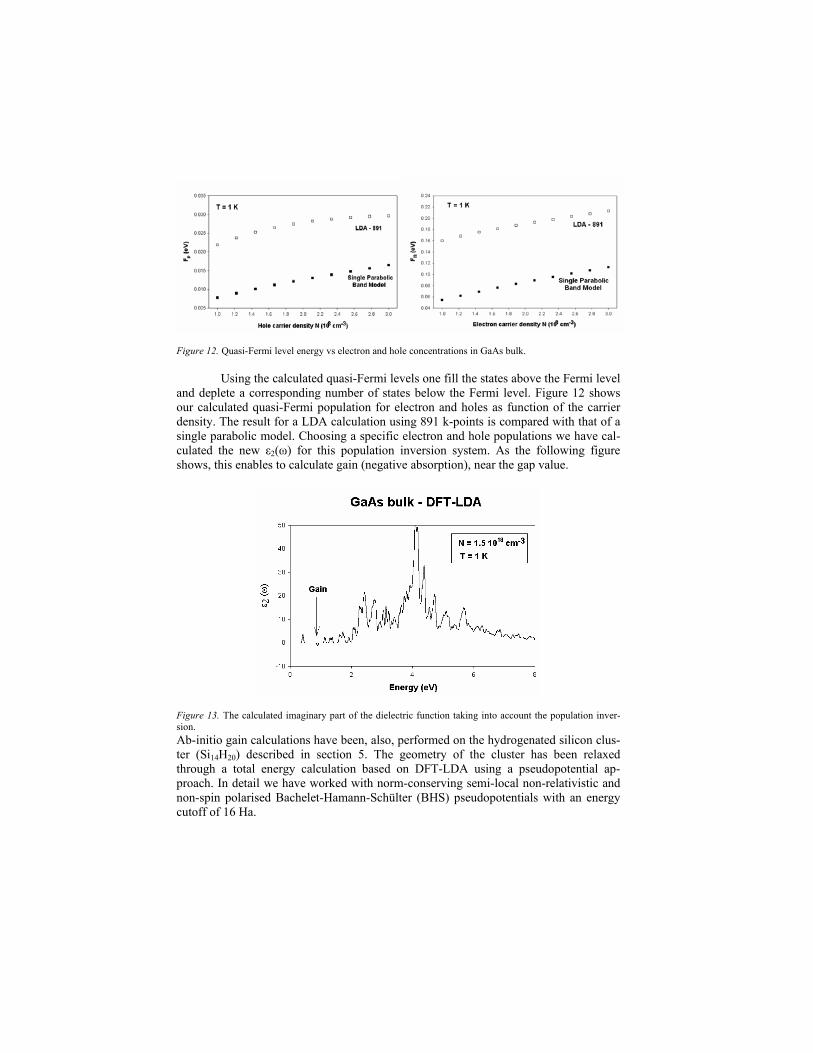
Figure 12. Quasi-Fermi level energy vs electron and hole concentrations in GaAs bulk.
Using the calculated quasi-Fermi levels one fill the states above the Fermi level and deplete a corresponding number of states below the Fermi level. Figure 12 shows our calculated quasi-Fermi population for electron and holes as function of the carrier density. The result for a LDA calculation using 891 k-points is compared with that of a single parabolic model. Choosing a specific electron and hole populations we have cal-culated the new ε2(ω) for this population inversion system. As the following figure shows, this enables to calculate gain (negative absorption), near the gap value.
Figure 13. The calculated imaginary part of the dielectric function taking into account the population inver-sion. Ab-initio gain calculations have been, also, performed on the hydrogenated silicon clus-ter (Si14H20) described in section 5. The geometry of the cluster has been relaxed through a total energy calculation based on DFT-LDA using a pseudopotential ap-proach. In detail we have worked with norm-conserving semi-local non-relativistic and non-spin polarised Bachelet-Hamann-Schülter (BHS) pseudopotentials with an energy cutoff of 16 Ha.

Figure 14. Top left) Calculated enegy levels at the Γ point in the brillouin zone for the Si14H20 cluster. The energies are refered to the higher valence level. Top right) Imaginary part of the dielectric function for the Si14H20 cluster. Bottom left) Calculated absorption spectra for the Si14H20 cluster after having depleted the highest valence level and filled the lowest conduction level with a 2x1019 cm-3 electron-hole pair density. Bot-tom right) Calculated absorption spectra for the Si14H20 cluster after having depleted the highest valence level and filled the second conduction level with a 2x1019 cm-3 electron-hole pair density.
The electronic and optical properties have been computed: figure 14 (Top left) shows the energy levels at the Γ point, actually, in the case of clusters, where the num-ber of atoms is really small, we haven’t a real band structure but simply discrete energy levels. The computed energy gap is of 4.1 eV. Starting from the electronic results and through the theory of inter-band transitions we have computed the imaginary part of the dielectric function ε2 (see Fig. 14 Top right) in the optical limit. The gaussian brodening of 0.05 used to produce this figure hide the real onset of the function that correspond to a transition energy of 4.22 eV, bigger that the gap value. This is due to the fact that the transition probability between the highest valence level and the lowest conduction level is null: this transition is forbidden. To perform gain calculations we have considered two different models of population inversion: in the first case (see Fig. 14 Bottom left) we have depleted the highest valence level and filled the lowest conduction level with a 2x1019 cm-3 electron-hole pair density at a temperature of 10 K, while in the second one (see Fig. 14 Bottom right) we have depleted the highest valence level and filled the sec-ond conduction level in the same conditions of carrier density and temperature.
As can be clearly seen there are in both cases a lot of new peaks in the low en-ergy range with respect to the ground state ε2; these are due to the new inter- and intra-band transitions induced by the considered population inversion. In the first case no gain is present; actually, as previously said, the transition between the involved states is

forbidden. In the second case, instead, we can observe two negative absorption peaks; the gain observed at 0.12 eV is due to the intra-band transition from the second to the first conduction levels, while the 4.22 eV negative peak is a consequence of the inter-band transition from the second conduction level to the highest valence level. This cal-culation, simply based on the optical matrix elements between the states involved in the transition, can give an idea of the possible deexcitation paths. 7. Structural, electronic and optical properties of Si nanocrystals embedded in a SiO2 matrix
Figure 15. Stick and ball pictures of the final optimized structure of Si10 in SiO2. The dark gray spheres repre-sent O atoms, light gray Si and white the Si atoms of the nanocrystal. In this section our goal has been to build up a simple model to study, for the first time, the properties of Si nanocrystals embedded in SiO2 matrix from a theoretical point of view [22,23]. We wanted at same time two fundamental qualities: a silicon skeleton with a crystalline behavior for simulating the Si-nc and the simplest Si-SiO2 interface, with the minimum number of dangling bonds or defects.
For these reasons we have started with a cubic cell (l=14.32 Å ) of SiO2 betac-ristobalite (BC) which is well known to have one of the simplest Si/SiO2 interface be-cause of its diamond-like structure [33]. We get the cell repeating two times along each cartesian axe the unit cell of SiO2 BC. Then we obtained a small dot simply deleting some oxygen atoms of the SiO2 matrix and linking together the silicon atoms left with dangling bonds, as shown in Fig. 15. In this way we have built an initial supercell of 64 Si and 116 O atoms with 10 Si bonded together to form a small crystalline skeleton (Td

interstitial symmetry) with a very highly strained bond length with respect to the bulk case: 3.1 Å. On this system we have performed geometry optimization runs leaving free to relax all the atoms and all the cell parameters.
Fig. 15 shows the final relaxed supercell structure after the geometry optimiza-tion for the Si-nc (Si10) in SiO2. Looking at the dot behavior we find that the skeleton is still crystalline-like (diamond) with a Si-Si bond length of 2.67 Å, that means a strain of 14% respect to the bulk case. This rearrangement causes a complex deformation of the SiO2 matrix around the dot both in bond lengths and angles.
Figure 16. a) Band structure along high symmetry points of the BZ for the Si NC in SiO2 at relaxed geometry. b) Absorption spectrum of the Si NC in SiO2. The vertical line indicates the calculated Eg for SiO2 BC (bulk).
It seems as if the lack of oxygen atoms and the compression of the dot volume deter-mine an empty region that the SiO2 structure tends to fill up stressing bonds and angles in various ways. Nevertheless the deformation doesn’t affect the entire SiO2 matrix. It is actually possible to find still a good BC crystalline structure, in terms of angles and bond-length, at a distance from the dot’s atoms of 0.8-0.9 nm. This means that the dot is surrounded by a cap-shell of stressed SiO2 BC with a thickness of about 1 nm which progressively goes towards a pure crystalline BC. This view is also supported by the analysis of the electronic properties as described below.
Fig. 16a shows the results for the electronic properties of the relaxed structure. The calculated Eg is 2.07 eV, that must be compared with the value of 5.84 eV for the Eg

of BC SiO2 (bulk) (calculated with the same technique). The strong reduction is origi-nated by the presence, at the valence and conduction band edges, of confined, flat, states completely related to the Si-nc, whereas deep inside the valence and conduction bands the more k-dispersed states related to the SiO2 matrix are still present.
In Fig. 17 the HOMO and LUMO isosurfaces at fixed value are reported; we clearly see that the distribution is totally confined in the Si-nc region with some weight on the interface O atoms. These dot-related states originate strong absorption features in the optical region as witnessed from Fig. 16b. These features are entirely new and can be at the origin of the photoluminescence observed in the red optical region for Si-nc immersed in a SiO2 matrix [34].
Figure 17. Isosurfaces at fixed value (25% of max. amplitude) of the square modulus of highest occupied (HOMO) and lowest unoccupied (LUMO) Kohn-Sham orbitals for the Si NC in the SiO2 matrix. Moreover our result concerning the role of both Si-nc and the interface Si-O region with respect to the absorption process is in close agreement with the X-ray absorption fine structure measurements [35] that indicate the presence of an intermediate region be-tween Si-nc and the SiO2 matrix that participates in the light emission process [36].
8. Summary The present work aims at answer a very important question related to the origin of the striking optical properties of Si nanoclusters. We have demonstrated, by first principle calculations that the structural, electronic and optical properties of Si-nc strongly de-pend not only on the dimensions of the nanocrystals, i.e. on the quantum confinement, but also on the different passivation regimes, i.e. on the interface region. Starting from
H-covered Si-nc we have shown that single bonded O atoms originate small variations in the electronic properties and huge changes in the structural properties. On the con-trary double bonded O atoms make a small contribution to geometry variations, but a strong reduction in the energy gap. Moreover a non-linear reduction of the energy gap with the double bonds number has been found. In the case of Si-nc embedded in SiO2 matrix, our results show that the SiO2 cage is only slightly deformed by the presence of the Si-nc, that new electronic states are originated within the SiO2 band gap and that both the Si-nc region and the interface region play a role in the optical properties. These results help to clarify the experimental outcomes regarding the electronic and optical properties of heavily oxidized Si-nc and the structural, electronic and optical properties of Si-nc dispersed in SiO2. Hartree-Fock calculations for the ground and excited states of the Si-nc have been interpreted within a four level model system, which has also been used to construct a rate equation system that fits qualitatively the experimental data on gain in Si-nc embedded in a SiO2 matrix. Finally preliminary results of ab-initio calcula-tion of gain in Si nanostructures have been presented.
This paper is dedicated to the memory of Claudio Bertarini. Claudio, former member of our research group, perished September 2001 in a car crash. We all remem-ber his active presence, his scientific and computational skill, his unforgettable silent smile. Financial support by INFM-PRA Ramses and CNR PF MADESSII is acknowl-edged. References 1. Sze, S. M. (1998) Modern Semiconductor Device Physics, John Wiley & Sons. 2. Davies, J. H. (1998) The Physics of Low-Dimensional Semiconductors: An Introduction , Cambridge University Press, Cambridge. 3. Borisenko, V. E. Filonov, A. B. Gaponenko, S. V. Gurin, V. S. (2001) Physics, Chemistry, and Appli-cation of Nanostructures, World Scientific, Singapore. 4. Tsu, R. (2000) Appl. Phys. A 71, 391. 5. Canham, L. T. (1990) Silicon quantum wire array fabrication by electrochemical and chemical dissolu-tion of wafers, Appl. Phys. Lett. 57, 1046. 6. Bensahel, D. Canham, L. T. Ossicini, S. (1993) Optical Properties of Low Dimensional Silicon Struc-tures, Kluwer, Dordrecht, Amsterdam. 7. Hamilton, B. (1995) Porous silicon, Semicond. Sci. Technol. 10, 1187. 8. Kanemitsu, Y. (1995) Light emission from porous silicon and related materials, Phys. Rep. 263, 1. 9. John, G. S. and Singh, V. A. (1995) Porous silicon: theoretical studies, Phys. Rep. 263, 93. 10. Canham, L. (1997) Properties of Porous Silicon, INSPEC, The Institution of Electrical Engineers, Lon-don. 11. Cullis, A.G. Canham, L. T. and Calcott, P.D. J. (1997) The structural and luminescence properties of porous silicon, J. Appl. Phys. 82, 909. 12. Bisi, O. Ossicini, S. Pavesi, L. (2000) Porous silicon: a quantum sponge structure for silicon based optoelectronic, Surf. Sci. Reports 38, 5. 13. Pavesi, L. Dal Negro, L. Mazzoleni, C. Franzò G. and Priolo, F. (2000) Optical gain in silicon nanocrystals, Nature 408, 440. 14. Dal Negro, L. Cazzanelli M. Daldosso, N. Gaburro, Z. Pavesi, L. Priolo, F. Pacifici, D. Franzò, G and Iacona, F. (2002) in press Stimulated emission in plasma enhanced chemical vapour deposited silicon nanocrystals, Physica E. 15. Dewar, M. J. S. et al. (1985) , J. Am. Chem. Soc. 107, 3902. 16. Baierle, R. J. Caldas, M. J. Molinari, E. and Ossicini, S (1997) Optical emission from small Si particles, Solid State Comm. 102, 545. 17. Caldas, M. J. (2000) Si nanoparticles as a model for porous Si, phys. stat. sol. (b), 217, 641.

18. Dreizler, R.M. and Gross, E.K.U. (1990) Density Functional Theory. An Approach to the Quantum Many-Body Problem, Springer-Verlag, Berlin. 19. Kleinman, L. and Bylander, D.M. (1982) Efficacious Form for Model Pseudopotentials, Phys. Rev. Lett. 48, 1425. 20. Bockstedte, M. Kley, A. Neugebauer, J. and Scheffler, M. (1997) Comput. Phys. Commun. 107, 187. 21. Vanderbilt, D. (1990) Soft self-consistent pseudopotentials in a generalized eigenvalue formalism, Phys. Rev. B 41. 7892. 22. Luppi, M. and Ossicini, S. (2002) in press Oxygen role on the structural and optoelectronic properties of silicon nanodots, phys. stat. sol. (a). 23. Luppi, M. and Ossicini, S. (2002) in press Oxygen role on the optoelectronic properties of silicon nanodots, Material Science and Engineering B. 24. Milman, V. Winkler, B. White, J. A. Pickard, C. J. Payne, M. C. Akhmatskaya, E. V. Nobes, R. H. (2000) Int. J. Quant. Chem. 77, 895. 25. Perdew, J. P. (1986) Density-functional approximation for the correlation energy of the inhomogeneous electron gas, Phys. Rev B 33, 8822. 26. Perdew, J. P. Burke, K. and Ernzerhof, M. (1996) Generalized Gradient Approximation Made Simple, Phys. Rev. Lett. 77 3865; (1997) 78, 1396. 27. Fisher T.H., Almlöf, J. (1992) J. Phys. Chem. 96, 9768. 28. Filonov, A. B., Ossicini, S., Bassani, F. Arnaud D’Avitaya, F. (2002) Effect of oxygen on the optical properties of small silicon pyramidal clusters, Phys. Rev B 65, 195317. 29. Vasiliev, I. Chelikowsky, J. R. and Martin, R. M. (2002) Surface oxidation effects on the optical proper-ties of silicon nanocrystals, Phys. Rev. B 65, 121302(R). 30. Wolkin, M. V. Jorne, J. Fauchet, P. M. Allan, G. and Delerue, C. (1999) Electronic States and Lumines-cence in Porous Silicon Quantum Dots: The Role of Oxygen, Phys. Rev. Lett. 82, 197. 31. van Buuren, T. Dinh, L. N. Chase, L. L. Sekhaus, W. J. Terminello, L. J. (1998) Changes in the Elec-tronic Properties of Si Nanocrystals as a Function of Particle Size, Phys. Rev. Lett. 80, 3803. 32. Valenta, J. Juhasz, R and Linnros, J. (2002) Photoluminescence spectroscopy of single quantum dots, Appl. Phys. Lett. 80, 1070. 33. Kageshima, H. Shiraishi, K. (1996) Double bond formation mechanism for passivating Si/SiO2 interface states, Scheffler, M. Zimmermann R., Proc. 23rd Int. Conf. Phys. Semicon., World Scientific, Singapore, p. 903. 34. Prakash, G. V. Daldosso, N. Degoli, E. Iacona, F. Cazanelli, M. Gaburro, Z. Puker, G. Dalba, G. Rocca, F. Ceretta Moreira, E. Franzò, G. Pacifici, D. Priolo, F. Arcangeli, C. Filonov, A. B. Ossicini, S. and Pavesi, L., (2001) Structural and Optical Properties of Silicon Nanocrystals Grown by Plasma-Enhanced Chemical Vapor Deposition, J. Nanosci. Nanotech. 1, 159. 35. Daldosso, N. Dalba, G. Grisenti, R. Dal Negro, L. Pavesi, L. Rocca, F. Priolo, F. Franzò, G. Pacifici, D. and Iacona, F. (2002) in press X-ray absorption study of light emitting silicon nanocrystals, Physica E. 36. Daldosso, N., Luppi, M. Ossicini, S. Degoli, E., Magri, R. Dalba, G. Fornasini, P. Grisenti, R. Rocca, F. Pavesi, L. Priolo, F. and Iacona, F (2002) submitted Role of the interface region on the optoelectronic properties of silicon nanocrystals embedded in SiO2, Phys. Rev. B