Silicon quantum dot nanostructures for tandem photovoltaic cells
9
Silicon quantum dot nanostructures for tandem photovoltaic cells Gavin Conibeer ⁎ , Martin Green, Eun-Chel Cho, Dirk König, Young-Hyun Cho, Thipwan Fangsuwannarak, Giuseppe Scardera, Edwin Pink, Yidan Huang, Tom Puzzer, Shujuan Huang, Dengyuan Song, Chris Flynn, Sangwook Park, Xiaojing Hao, Daniel Mansfield ARC Photovoltaics Centre of Excellence, University of New South Wales, Sydney, NSW 2052, Australia Available online 16 January 2008 Abstract Tandem PV cells – with their increased efficiency due to a multi-band gap approach – usually involve expensive materials and fabrication. Thin film approaches, with an engineered variation in band gap through the use of quantum confinement in Si quantum dots, offer a cheaper alternative. Presented are characterisation and modelling data on fabrication of such Si and Sn QD nanostructures in various dielectric matrices by self-organised thin film deposition, with demonstrated confined energy levels of 1.7 eV for 2 nm diameter QDs. This being the optimum energy for an upper tandem cell element. © 2008 Elsevier B.V. All rights reserved. Keywords: Quantum dots; Thin film; Third generation; Quantum confinement 1. Third generation approaches The two most important power loss mechanisms in single- band gap photovoltaic cells are the inability to absorb photons with energy less than the band gap (1 in Fig. 1), and thermalisation of photon energy exceeding the band gap, (2 in Fig. 1). There have been proposed three families of approaches for tackling them [1]: (a) increasing the number of band gaps; (b) capturing carriers before thermalisation; and (c) multiple carrier pair generation per high energy photon or single carrier pair generation with multiple low energy photons. Of these, tandem cells, an implementation of strategy (a), are the only ones which have been realised with efficiencies exceeding the limit for a single band gap device. For an ideal device this is given by Shockley and Queisser using detailed balance as 31%. The losses (3) and (4) in Fig. 1 can be made arbitrarily small, at least in principle, and the radiative recombination loss can not be avoided for a time reciprocal device. Hence third generation devices concentrate on reducing losses (1) and (2). Another consideration for the concept of a third generation device is that it uses abundant materials that do not cause toxicity in the environment and that it be made by approaches amenable to large scale mass production — in practice this generally means thin film deposition techniques [2]. 2. The “all-Si” tandem cell Silicon is a benign readily available material, which is widely used for solar cell fabrication. Silicon also has a band gap which is close to optimal not only for a standard, single p–n junction cell (a little too low) but also for the bottom cell in a 2-cell or even a 3-cell tandem stack (a little too high). The radiative efficiency limit for a single junction silicon cell is 29%. This increases to 42.5% and 47.5% for 2-cell and 3-cell tandem stacks respectively. For an AM1.5 solar spectrum the optimal band gap of the top cell required to maximize conversion efficiency is ∼ 1.7 to 1.8 eV for a 2-cell tandem with a Si bottom cell and 1.5 eV and 2.0 eV for the middle and upper cells for a 3- cell tandem [3]. A cell based entirely of silicon and its dielectric compounds with other abundant elements (i.e. its oxides, nitrides or carbides) fabricated with thin film techniques, is therefore advantageous in terms of potential for large scale manufactur- ability and in long term availability of its constituents. Such thin film implementation implies low temperature deposition with- out melt processing, it hence also involves imperfect crystal- lisation with high defect densities. Hence devices must be thin Available online at www.sciencedirect.com Thin Solid Films 516 (2008) 6748 – 6756 www.elsevier.com/locate/tsf ⁎ Corresponding author. Tel.: +61 2 9385 7858; fax: +61 2 9385 5412. E-mail address: [email protected] (G. Conibeer). 0040-6090/$ - see front matter © 2008 Elsevier B.V. All rights reserved. doi:10.1016/j.tsf.2007.12.096
-
Upload
independent -
Category
Documents
-
view
1 -
download
0
Transcript of Silicon quantum dot nanostructures for tandem photovoltaic cells

Available online at www.sciencedirect.com
008) 6748–6756www.elsevier.com/locate/tsf
Thin Solid Films 516 (2
Silicon quantum dot nanostructures for tandem photovoltaic cells
Gavin Conibeer ⁎, Martin Green, Eun-Chel Cho, Dirk König, Young-Hyun Cho,Thipwan Fangsuwannarak, Giuseppe Scardera, Edwin Pink, Yidan Huang, Tom Puzzer,
Shujuan Huang, Dengyuan Song, Chris Flynn, Sangwook Park, Xiaojing Hao, Daniel Mansfield
ARC Photovoltaics Centre of Excellence, University of New South Wales, Sydney, NSW 2052, Australia
Available online 16 January 2008
Abstract
Tandem PV cells – with their increased efficiency due to a multi-band gap approach – usually involve expensive materials and fabrication.Thin film approaches, with an engineered variation in band gap through the use of quantum confinement in Si quantum dots, offer a cheaperalternative. Presented are characterisation and modelling data on fabrication of such Si and Sn QD nanostructures in various dielectric matrices byself-organised thin film deposition, with demonstrated confined energy levels of 1.7 eV for 2 nm diameter QDs. This being the optimum energyfor an upper tandem cell element.© 2008 Elsevier B.V. All rights reserved.
Keywords: Quantum dots; Thin film; Third generation; Quantum confinement
1. Third generation approaches
The two most important power loss mechanisms in single-band gap photovoltaic cells are the inability to absorb photonswith energy less than the band gap (1 in Fig. 1), andthermalisation of photon energy exceeding the band gap, (2 inFig. 1). There have been proposed three families of approachesfor tackling them [1]: (a) increasing the number of band gaps;(b) capturing carriers before thermalisation; and (c) multiplecarrier pair generation per high energy photon or single carrierpair generation with multiple low energy photons. Of these,tandem cells, an implementation of strategy (a), are the onlyones which have been realised with efficiencies exceeding thelimit for a single band gap device. For an ideal device this isgiven by Shockley and Queisser using detailed balance as 31%.
The losses (3) and (4) in Fig. 1 can be made arbitrarily small,at least in principle, and the radiative recombination loss can notbe avoided for a time reciprocal device. Hence third generationdevices concentrate on reducing losses (1) and (2). Anotherconsideration for the concept of a third generation device is thatit uses abundant materials that do not cause toxicity in theenvironment and that it be made by approaches amenable to
⁎ Corresponding author. Tel.: +61 2 9385 7858; fax: +61 2 9385 5412.E-mail address: [email protected] (G. Conibeer).
0040-6090/$ - see front matter © 2008 Elsevier B.V. All rights reserved.doi:10.1016/j.tsf.2007.12.096
large scale mass production — in practice this generally meansthin film deposition techniques [2].
2. The “all-Si” tandem cell
Silicon is a benign readily available material, which is widelyused for solar cell fabrication. Silicon also has a band gap whichis close to optimal not only for a standard, single p–n junctioncell (a little too low) but also for the bottom cell in a 2-cell oreven a 3-cell tandem stack (a little too high). The radiativeefficiency limit for a single junction silicon cell is 29%. Thisincreases to 42.5% and 47.5% for 2-cell and 3-cell tandemstacks respectively. For an AM1.5 solar spectrum the optimalband gap of the top cell required to maximize conversionefficiency is∼ 1.7 to 1.8 eV for a 2-cell tandem with a Si bottomcell and 1.5 eVand 2.0 eV for the middle and upper cells for a 3-cell tandem [3].
A cell based entirely of silicon and its dielectric compoundswith other abundant elements (i.e. its oxides, nitrides orcarbides) fabricated with thin film techniques, is thereforeadvantageous in terms of potential for large scale manufactur-ability and in long term availability of its constituents. Such thinfilm implementation implies low temperature deposition with-out melt processing, it hence also involves imperfect crystal-lisation with high defect densities. Hence devices must be thin
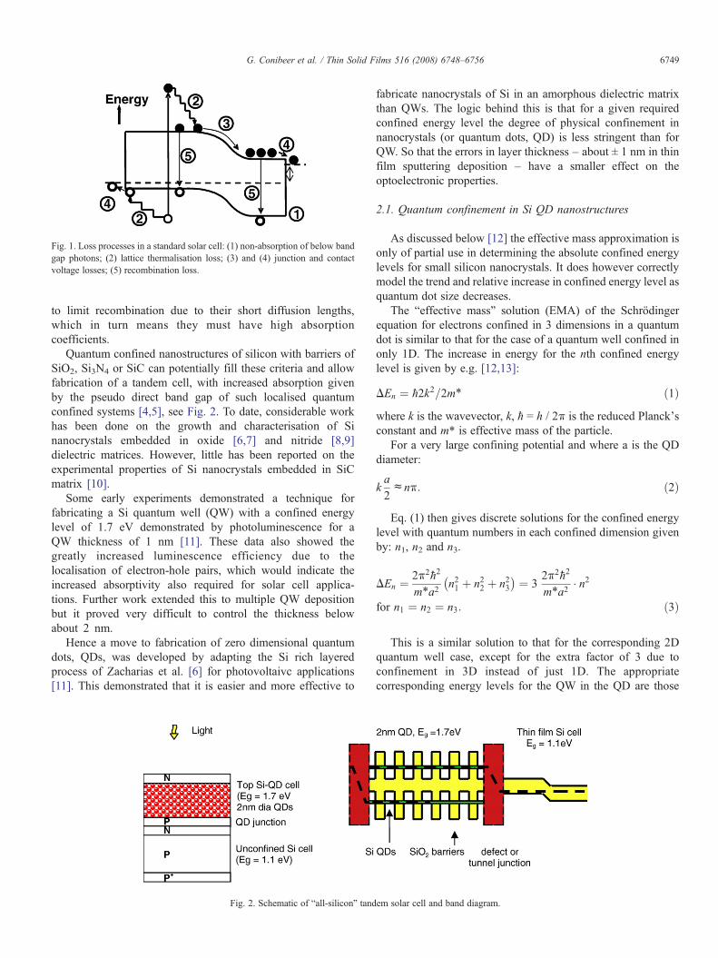
Fig. 1. Loss processes in a standard solar cell: (1) non-absorption of below bandgap photons; (2) lattice thermalisation loss; (3) and (4) junction and contactvoltage losses; (5) recombination loss.
6749G. Conibeer et al. / Thin Solid Films 516 (2008) 6748–6756
to limit recombination due to their short diffusion lengths,which in turn means they must have high absorptioncoefficients.
Quantum confined nanostructures of silicon with barriers ofSiO2, Si3N4 or SiC can potentially fill these criteria and allowfabrication of a tandem cell, with increased absorption givenby the pseudo direct band gap of such localised quantumconfined systems [4,5], see Fig. 2. To date, considerable workhas been done on the growth and characterisation of Sinanocrystals embedded in oxide [6,7] and nitride [8,9]dielectric matrices. However, little has been reported on theexperimental properties of Si nanocrystals embedded in SiCmatrix [10].
Some early experiments demonstrated a technique forfabricating a Si quantum well (QW) with a confined energylevel of 1.7 eV demonstrated by photoluminescence for aQW thickness of 1 nm [11]. These data also showed thegreatly increased luminescence efficiency due to thelocalisation of electron-hole pairs, which would indicate theincreased absorptivity also required for solar cell applica-tions. Further work extended this to multiple QW depositionbut it proved very difficult to control the thickness belowabout 2 nm.
Hence a move to fabrication of zero dimensional quantumdots, QDs, was developed by adapting the Si rich layeredprocess of Zacharias et al. [6] for photovoltaivc applications[11]. This demonstrated that it is easier and more effective to
Fig. 2. Schematic of “all-silicon” tand
fabricate nanocrystals of Si in an amorphous dielectric matrixthan QWs. The logic behind this is that for a given requiredconfined energy level the degree of physical confinement innanocrystals (or quantum dots, QD) is less stringent than forQW. So that the errors in layer thickness – about ± 1 nm in thinfilm sputtering deposition – have a smaller effect on theoptoelectronic properties.
2.1. Quantum confinement in Si QD nanostructures
As discussed below [12] the effective mass approximation isonly of partial use in determining the absolute confined energylevels for small silicon nanocrystals. It does however correctlymodel the trend and relative increase in confined energy level asquantum dot size decreases.
The “effective mass” solution (EMA) of the Schrödingerequation for electrons confined in 3 dimensions in a quantumdot is similar to that for the case of a quantum well confined inonly 1D. The increase in energy for the nth confined energylevel is given by e.g. [12,13]:
DEn ¼ ћ2k2=2m⁎ ð1Þwhere k is the wavevector, k, ћ = h / 2π is the reduced Planck'sconstant and m⁎ is effective mass of the particle.
For a very large confining potential and where a is the QDdiameter:
ka2cnk: ð2Þ
Eq. (1) then gives discrete solutions for the confined energylevel with quantum numbers in each confined dimension givenby: n1, n2 and n3.
DEn ¼ 2k2ћ2
m⁎a2n21 þ n22 þ n23� � ¼ 3
2k2ћ2
m⁎a2� n2
for n1 ¼ n2 ¼ n3: ð3Þ
This is a similar solution to that for the corresponding 2Dquantum well case, except for the extra factor of 3 due toconfinement in 3D instead of just 1D. The appropriatecorresponding energy levels for the QW in the QD are those
em solar cell and band diagram.

Fig. 4. Experimental energy gaps of three-dimensionally confined Sinanocrystals in SiO2 and SiNx (300°K) from several authors [21–23,8,24].
6750 G. Conibeer et al. / Thin Solid Films 516 (2008) 6748–6756
that are non-degenerate with the same quantum number. Hencefor nQW in a QW the corresponding level is when n1 = n2 = n3 =nQW.
Hence for a given size of confinement, the QD hasconfined energy levels 3× those of a QW. Or put another way,for a given confined energy level a QD has a diameter whichis √3× the width of the corresponding QW. [Strictly, this isfor a cubic QD. For a spherical QD of diameter a theconfinement is slightly greater and the factor slightly largerthan √3.]
In this calculation, the isotropic conduction-band effectivemass is taken as the most appropriate for Si, with eachconduction band valley giving rise to a 2-fold degeneracy in thetransverse directions, this gives an effective isotropic massgiven by [14,15]:
1m⁎
¼ 13
1ml
þ 2mt
� �
where ml and mt are longitudinal and transverse masses,respectively. Substituting values for silicon, the calculatedground state energy corresponds to an equivalent isotropic massme⁎ = 0.27mo and mh⁎ = 0.59mo for electrons and holes,respectively [14]. Substituting these values in Eq. (3) gives, forthe first quantised ground state energy:
E1 ¼ Eg þ DE1 ¼ Eg þ 418:08a2
þ 191:32a2
¼ 609:408a2
ð4Þ
where a is in Angstroms and E1 and Eg (the bulk band gap ofSi) are in eV.
The results from this calculation are shown in Fig. 3 togetherwith data from photoluminescence on our QD nanostructures inSiO2 and those of other authors [16–18]. This shows adecreasingly inaccurate prediction of the confined energylevel by the EMA as the QD size decreases.
Part of the explanation for this is that for a non-infiniteconfining barrier potential, i.e. in a real dielectric matrix, the
Fig. 3. Measured PL energies for our own and others' data as a function of QDsize [12,16–18]. Also shown is the EMA calculation using Eq. (4) [12].
approximation of Eq. (2) is no longer valid. k is then given bythe implicit equation:
ka2¼ nk� sin�1 ћk=
ffiffiffiffiffiffiffiffiffiffiffiffiffiffi2m⁎V0
p� �ð5Þ
where V0 is the corresponding barrier height. The value of En isreduced as given by [19] p578:
Enc3 � 2 � k2ћ2
m4a2n2= 1þ ћ
a=2ffiffiffiffiffiffiffiffiffiffiffiffiffiffi2m⁎V0
p� �2
ð6Þ
This is always less than En from Eq. (3). Hence, smallconfinement barriers will reduce the confinement energy.However as discussed below PL data for confined energylevels does not match Eq. (6). A possible approach is anempirical modification of the factor m⁎V0 to better fit thedata.
We have also observed that the photoluminescence peaksfrom Si QDs in nitride are more blue-shifted than that of Si QDsin oxide. Fig. 4 shows a comparison of the two furthercompared to the results of other workers for PL peak energiesfrom Si QDs dispersed in oxide [20,18,21] and nitride [8,22].This shows that PL peak energies of Si QDs in oxide are lessthan 2.0 eV while Si QDs in nitride have peak energies less than3.0 eV.
Our PL results for Si QDs are in quite good agreement withthe results from other authors [20,18,21,22,8] (see Fig. 4) andare also qualitatively consistent with the results from ab-initiomodelling [23], which we have carried out for the confinedenergy levels in Si QD consisting of a few hundred atoms. Thisuses Gaussian03, a Density Functional–Hartree Fock based ab-initio program. Fig. 5 shows some results for ground stateconfined energy levels (actually HOMO–LUMO gaps) for Sinanocrystals of various sizes terminated with either –H (theclosest to vacuum for a terminated surface); –OH groups; and –NH2 groups (using a nearest neighbour assumption these twoare assumed analogous to a SiO2 and Si3N4 matrix). These showthe expected increasing confinement energy with decreasing

Fig. 5. Modelled Si35(OH)36 [left] and Si35(NH2)36 [middle] nanoclusters before energy level optimisation. The Si core volume corresponds to dQD=11 Å. The graphon the right shows the highest occupied MO (HOMO) – lowest unoccupied MO (LUMO) gaps of –H, –OH and –NH2 – terminated Si cores as f(dQD).
Fig. 6. Bulk band alignments between crystalline silicon and its carbide, nitrideand oxide.
6751G. Conibeer et al. / Thin Solid Films 516 (2008) 6748–6756
QD size but also show the reduction in energy on going from aQD effectively in vacuum to one embedded in a dielectric [23].
It is also seen that the amino terminated QDs (simulatingnitride) has energies about 0.5 eV greater than the hydroxylterminated ones (simulating oxide). This is qualitativelyconsistent both with out own PL results for QDs in oxide andnitride and with the results of the other authors shown in Fig. 4.This is consistent with an explanation for the enhanced energiesof QDs in nitride given by Yang et al. [24], that the reason for itis due to better passivation of Si QDs by nitrogen atomseliminating the strain at the Si/Si3N4 interface.
However, the PL data is in disagreement with the modifiedEMA solution in Eq. (6), as the barrier height, V0, of nitride issmaller than oxide and hence Eq. (6) would give a smallerconfined energy level not a larger one. This elucidates theunderlying problem which is that the EMA breaks down forsmall QDs. Further Gaussian modelling has demonstrated thisto be the case. This breakdown is not surprising as the Blochassumption in the EMA of a carrier wavefunction varying onlyvery gradually across the periodic potential of the lattice, is nolonger valid when the wavefunction is associated with a smallspatial volume approaching the size of the lattice spacing, as in asmall QD. We are working on a calibration for a modifiedeffective mass using the Gaussian modelling, in order to modifythe EMA. This parameter will vary with the QD size and withthe species at the interface, as for small QDs the lowest energystates dominate the confined energy levels [23].
3. Si QD superlattice formation
Transport properties in a QD superlattice are expected todepend on the matrix in which the silicon quantum dots areembedded. As shown in Fig. 6, different matrices producedifferent transport barriers between the Si dot and the matrix,with tunnelling probability heavily dependent on the height ofthis barrier. Si3N4 and SiC give lower barriers than SiO2
allowing larger dot spacing for a given tunnelling current.The wave function of an electron confined to a spherical dot
penetrates into the surrounding material, decreasing exponen-tially into the barrier. The slope of this exponential decay and
hence the barrier to tunnelling between quantum dots is reducedfor a lower barrier height material. This is because – from aconsideration of transmission/reflection probability – thetunnelling probability Te through a square potential welldepends exponentially on three parameters, the barrier widthd (i.e. the spacing between quantum dots); the square root ofthe barrier height seen by the electron (ΔE1/2 the energydifference between the conduction band edge of the matrix andthe confined energy level of the quantum dots = (Ec − En)
1/2);and the square root of the effective mass (m⁎)1/2 of the electronwithin the barrier. This gives approximately (e.g. [19] p244):
Tec16 exp �d
ffiffiffiffiffiffiffiffiffiffiffiffiffiffiffi8m⁎
ћ2DE
r( ): ð7Þ
Therefore the important parameter in determining the degreeof interaction between quantum dots is m⁎ΔEd2. As barrierheight decreases the barrier thickness for a given probabilityincreases, thus requiring lower dot density for a givenconductivity or higher conductivity for a given dot density. Inaddition as dot size decreases ΔE also decreases, thusincreasing Te and enhancing the effect further for smallerquantum dots [19]. The results suggest that dots in a SiO2
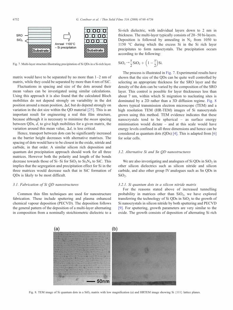
Fig. 7. Multi-layer structure illustrating precipitation of Si QDs in a Si-rich layer.
6752 G. Conibeer et al. / Thin Solid Films 516 (2008) 6748–6756
matrix would have to be separated by no more than 1–2 nm ofmatrix, while they could be separated by more than 4 nm of SiC.
Fluctuations in spacing and size of the dots around theirmean values can be investigated using similar calculations.Using this approach it is also found that the calculated Blochmobilities do not depend strongly on variability in the dotposition around a mean position,Δd, but do depend strongly onvariation in the dot size within the QD material [25]. This is animportant result for engineering a real thin film structure,because although it is necessary to minimise the mean spacingbetween QDs, d, to give high mobilities for a given matrix, thevariation around this mean value, Δd, is less critical.
Hence, transport between dots can be significantly increasedas the barrier height decreases with alternative matrixes. Thespacing of dots would have to be closest in the oxide, nitride andcarbide, in that order. A similar silicon rich deposition andquantum dot precipitation approach should work for all threematrices. However both the polarity and length of the bondsdecrease towards those of Si–Si for SiO2 to Si3N4 to SiC. Thisimplies that the segregation and precipitation effect for Si in thethree matrices would decrease such that in SiC formation ofQDs is likely to be most difficult.
3.1. Fabrication of Si QD nanostructures
Common thin film techniques are used for nanostructurefabrication. These include sputtering and plasma enhancedchemical vapour deposition (PECVD). The deposition followsthe general pattern of the deposition of a multi-layer alternatingin composition from a nominally stoichiometric dielectric to a
Fig. 8. TEM image of Si quantum dots in a SiO2 matrix with low mag
Si-rich dielectric, with individual layers down to 2 nm inthickness. The multi-layer typically consists of 20–50 bi-layers.Deposition is followed by annealing in N2 from 1050 to1150 °C during which the excess Si in the Si rich layerprecipitates to form nanocrystals. The precipitation occursaccording to the following:
SiOxYx2SiO2 þ 1� x
2
� �Si:
The process is illustrated in Fig. 7. Experimental results haveshown that the size of the QDs can be quite well controlled byselecting an appropriate thickness for the SRO layer and thedensity of the dots can be varied by the composition of the SROlayer. This control is possible for layer thicknesses less thanabout 7 nm, within which Si migration to nucleating sites isdominated by a 2D rather than a 3D diffusion regime. Fig. 8shows typical transmission electron microscope (TEM) and ahigh resolution TEM (HR-TEM) images of Si nanocrystalsgrown using this method. TEM evidence indicates that thesenanocrystals tend to be spherical – as surface energyminimisation would dictate – and at this scale would haveenergy levels confined in all three dimensions and hence can beconsidered as quantum dots (QDs) [4]. This is adapted from [6]for solar cells.
3.2. Alternative Si and Sn QD nanostructures
We are also investigating and analogues of Si QDs in SiO2 inother silicon dielectrics such as silicon nitride and siliconcarbide, and also other group IV analogues such as Sn QDs inSiO2.
3.2.1. Si quantum dots in a silicon nitride matrixFor the reasons stated above of increased tunnelling
probability in matrices other than SiO2, we have exploredtransferring the technology of Si QDs in SiO2 to the growth ofSi nanocrystals in silicon nitride by both sputtering and PECVD[9]. For sputtering, growth parameters are very similar to theoxide. The growth consists of deposition of alternating Si rich
nification (a) and HRTEM image showing Si {111} lattice planes.

Fig. 9. Gas phase in situ Si QDs dispersed in a Si3N4 matrix: (a) low magnification TEM and (b) high resolution TEM.
6753G. Conibeer et al. / Thin Solid Films 516 (2008) 6748–6756
and stoichiometric nitride layers. Annealing is carried out againat 1100 °C but with a pre-annealing at 500 °C, for the PECVDprocess, to drive off incorporated hydrogen. Again HRTEMimages showing even clearer nanocrystals have been obtained.To the best of our knowledge this was the first time layered SiQDs in nitride were grown [9].
We have now also extended the layered Si QDs in nitridetechnology to gas-phase in situ deposition. Fig. 9 shows in situSi QD dispersed in a nitride matrix. A stoichiometric Si3N4 layerand an in situ Si QD layer are alternately deposited on a Sisubstrate. This technique allows QDs to form during depositionwithout the need for a subsequent high temperature anneal. Weare actively studying this technique because it is a lowtemperature process — an important aspect for a robusttechnology.
3.2.2. Si QDs in silicon carbideFor a similar reason we are also investigating transfer of the
Si QD technology to a SiC matrix. SiC nanocrystals of a few nmdiameter in a SiO2 matrix were produced by silicon and carbonimplantation into thermal oxide [26]. However, to our knowl-edge, little has been reported on the experimental properties ofSi QDs embedded in a SiC matrix.
Fig. 10. Silicon-rich SiC precursor layer: (a) Raman spectra for various anneali
We have used an analogue of the oxide and nitride processesand precipitation of Si according to:
Si1�xCx ¼ x � SiCð Þ þ 1� 2xð Þ � Si: ð8Þ
Raman, TEM and XRD spectra for a silicon-rich Si0.75C0.25
precursor layer grown on a quartz substrate with subsequentannealing are shown in Fig. 10. There is clear evidence for theformation of nanocrystalline Si at an anneal temperature greaterthan 1000 °C. This is shown in the Raman peak at ∼ 508 cm−1
(red shifted from 520 cm−1 due to a nanocrystalline foldedBrillouin zone dispersion in k-space); TEM lattice fringespacing consistent with {111} Si planes; and XRD peaks at 2θ =28.4° with peak broadening indicating nanocrystals of 3–7 nm(estimated using the Scherrer equation). [It should be noted thatthe nanocrystal size determined by TEM is not necessarily thesame as that determined by XRD, because the volumes analysedin each case are very different.]
Other Si and C concentrations were tried. As the concentra-tion of C in SiC x is increased to the nearly stoichiometricSi0.495C0.505, Raman evidence for the stretching vibrationmodes of Si–C and C–C bonds can be easily identified [27].Increasing annealing temperature gives rise to increasing
ng temperatures; cross-sectional HRTEM image; and (c) X-ray diffraction.
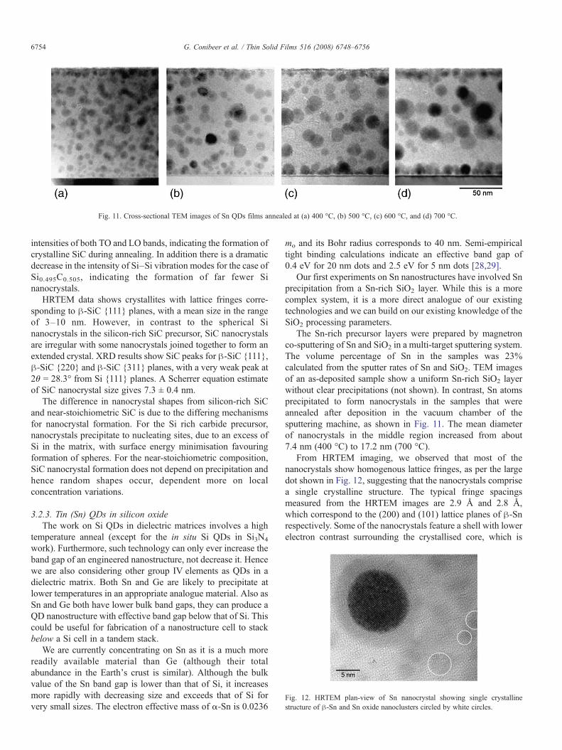
Fig. 11. Cross-sectional TEM images of Sn QDs films annealed at (a) 400 °C, (b) 500 °C, (c) 600 °C, and (d) 700 °C.
Fig. 12. HRTEM plan-view of Sn nanocrystal showing single crystallinestructure of β-Sn and Sn oxide nanoclusters circled by white circles.
6754 G. Conibeer et al. / Thin Solid Films 516 (2008) 6748–6756
intensities of both TO and LO bands, indicating the formation ofcrystalline SiC during annealing. In addition there is a dramaticdecrease in the intensity of Si–Si vibration modes for the case ofSi0.495C0.505, indicating the formation of far fewer Sinanocrystals.
HRTEM data shows crystallites with lattice fringes corre-sponding to β-SiC {111} planes, with a mean size in the rangeof 3–10 nm. However, in contrast to the spherical Sinanocrystals in the silicon-rich SiC precursor, SiC nanocrystalsare irregular with some nanocrystals joined together to form anextended crystal. XRD results show SiC peaks for β-SiC {111},β-SiC {220} and β-SiC {311} planes, with a very weak peak at2θ = 28.3° from Si {111} planes. A Scherrer equation estimateof SiC nanocrystal size gives 7.3 ± 0.4 nm.
The difference in nanocrystal shapes from silicon-rich SiCand near-stoichiometric SiC is due to the differing mechanismsfor nanocrystal formation. For the Si rich carbide precursor,nanocrystals precipitate to nucleating sites, due to an excess ofSi in the matrix, with surface energy minimisation favouringformation of spheres. For the near-stoichiometric composition,SiC nanocrystal formation does not depend on precipitation andhence random shapes occur, dependent more on localconcentration variations.
3.2.3. Tin (Sn) QDs in silicon oxideThe work on Si QDs in dielectric matrices involves a high
temperature anneal (except for the in situ Si QDs in Si3N4
work). Furthermore, such technology can only ever increase theband gap of an engineered nanostructure, not decrease it. Hencewe are also considering other group IV elements as QDs in adielectric matrix. Both Sn and Ge are likely to precipitate atlower temperatures in an appropriate analogue material. Also asSn and Ge both have lower bulk band gaps, they can produce aQD nanostructure with effective band gap below that of Si. Thiscould be useful for fabrication of a nanostructure cell to stackbelow a Si cell in a tandem stack.
We are currently concentrating on Sn as it is a much morereadily available material than Ge (although their totalabundance in the Earth's crust is similar). Although the bulkvalue of the Sn band gap is lower than that of Si, it increasesmore rapidly with decreasing size and exceeds that of Si forvery small sizes. The electron effective mass of α-Sn is 0.0236
mo and its Bohr radius corresponds to 40 nm. Semi-empiricaltight binding calculations indicate an effective band gap of0.4 eV for 20 nm dots and 2.5 eV for 5 nm dots [28,29].
Our first experiments on Sn nanostructures have involved Snprecipitation from a Sn-rich SiO2 layer. While this is a morecomplex system, it is a more direct analogue of our existingtechnologies and we can build on our existing knowledge of theSiO2 processing parameters.
The Sn-rich precursor layers were prepared by magnetronco-sputtering of Sn and SiO2 in a multi-target sputtering system.The volume percentage of Sn in the samples was 23%calculated from the sputter rates of Sn and SiO2. TEM imagesof an as-deposited sample show a uniform Sn-rich SiO2 layerwithout clear precipitations (not shown). In contrast, Sn atomsprecipitated to form nanocrystals in the samples that wereannealed after deposition in the vacuum chamber of thesputtering machine, as shown in Fig. 11. The mean diameterof nanocrystals in the middle region increased from about7.4 nm (400 °C) to 17.2 nm (700 °C).
From HRTEM imaging, we observed that most of thenanocrystals show homogenous lattice fringes, as per the largedot shown in Fig. 12, suggesting that the nanocrystals comprisea single crystalline structure. The typical fringe spacingsmeasured from the HRTEM images are 2.9 Å and 2.8 Å,which correspond to the (200) and (101) lattice planes of β-Snrespectively. Some of the nanocrystals feature a shell with lowerelectron contrast surrounding the crystallised core, which is

Fig. 13. (a) TEM image (cross-section) of tin quantum dot layers prepared in an oxide matrix; (b) HRTEM image (plan view) of a single layer of tin quantum dotsgiving additional information on lateral spacing. Inset: lattice plane image.
6755G. Conibeer et al. / Thin Solid Films 516 (2008) 6748–6756
thought to be a Sn oxide (Fig. 12). In addition, we observedsmall nanocrystals 2.5–5.0 nm in diameter with lower contrastfrom all vacuum annealed samples. When exposed for a fewminutes to the electron beam in the TEM chamber, thesenanocrystals revealed a clear fringe spacing of 3.3 Å ashighlighted by the white circles in Fig. 2, which corresponds tothe (110) lattice plane of SnO2.
With the intention of forming Sn nanocrystals of uniformsize, a multi-layer structure of Sn–SiO2 alternating with astoichiometric SiO2 layer was deposited. This was annealed atthe relatively low temperature of 400 °C for 1 h in the sputteringmachine vacuum chamber. Fig. 13 shows a plan-view TEMimage of a single layer of Sn QDs embedded in SiO2. Byannealing the sample at 600 °C in N2, a Sn nanocrystals size of3.5 ± 0.6 nm was obtained. The density of the nanocrystals andinter-nanocrystal spacing can be readily controlled by changingthe Sn content.
Further chemical, structural and optical characterisation isunderway along with further investigation of depositionproperties and possible photovoltaic application.
Fig. 14. XPS spectra of P–Si and P–O bonding from (a) SiO1.41 with phosphorus conc
4. Towards a Si QD nanostructure solar cell
Another requirement for a tandem cell element is thepresence of some form of junction for carrier separation —usually achieved with a p–n junction. Dopants such asphosphorous and boron alter the conductivity of bulk Si byseveral orders of magnitude. Important questions arise as towhether the dopants will continue to play a role similar to that inbulk semiconductors [30], or whether alternative methods ofwork function control will be required. It is not clear at presentwhether or not the doping of Si QDs provides the generation offree charge carriers [31]. The junction can either be a grown or adiffused p–n junction or a p–i–n junction with the superlatticeas the i-region. The latter requires careful control of the workfunctions (and therefore doping) of the p- and n-regions but alsomeans that it is not essential for the superlattice itself to bedoped.
In our experiments, phosphorus doping in the Si QDsuperlattices has been attempted using P2O5 co-sputteringduring the deposition of the silicon-rich oxide (Si and SiO2 co-
entration of 0.67 at.% and (b) SiO0.94 with phosphorus concentration of 0.27 at.%.

6756 G. Conibeer et al. / Thin Solid Films 516 (2008) 6748–6756
sputtering), which forms Si QDs upon high temperatureannealing. The P concentration in the silicon-rich oxide wasinitially chosen to be very high – much higher than dopingconcentrations – in order to increase the chances of detection.Phosphorus 2p X-ray photoelectron spectroscopy (XPS) spectrashow that P–O bonds (peak around 135 eV) and P–Si bondsand/or free phosphorus (peak around 129 eV) are observed fromhighly P-doped silicon-rich oxide (Fig. 14). SiO1.41 with 0.67 at% phosphorus shows both Si–P and O–P bonding, whilesilicon-rich SiO0.94 with 0.27 at % phosphorus shows only Si–Pbonding. The P concentration, when controlled in this way, washigh, in the range 0.26 at.%–3.02 at.%.
The XPS results indicate that the phosphorus in silicon-richoxide may exist in Si–P bonds inside Si QDs, however it isnecessary to carry out more analytical experiments for both n-type and p-type Si QDs in different matrices. The next stage isto attempt fabrication of hetero- and homo-junction structuresusing these doped Si QD nanostructures on transparent SiC andquartz substrates. These will allow a definite assessment of thephotovoltaic properties of these nanostructures.
5. Conclusions
Thin film tandem cells based on Si QD nanostructures satisfyboth the potential for increased efficiency and the thin filmpotentially low cost deposition required for Third Generationphotovoltaic devices. We have demonstrated confined energylevels in Si QD multi-layer structures in SiO2 and Si3N4
matrices and we are transferring the technology to Si QDs inSiC and also to Sn QDs in SiO2. The latter being particularlyimportant because of the potential for both lower processingtemperatures and lower confined energy levels. We have foundfrom ab-initio modelling that the reason the EMA is not aneffective method for predicting the confined energy levels of SiQDs in these structures (as determined by PL) is because of thebreakdown of the EMA and the Bloch picture for small QDs.
We have initiated doping studies of Si QD structures,although doping methods are not yet clear. Further work ondoping is continuing as well as a move towards test structures ofboth hetero- and homo-junctions on transparent substrates toinvestigate their photovoltaic behaviour.
Acknowledgements
The ARC Photovoltaics Centre of Excellence is funded bythe Australian Research Council. The authors also acknowledgethe support of the Global Climate and Energy Project (GCEP),administered by Stanford University, for helping to fund thiswork.
References
[1] J. Nelson, The Physics of Solar Cells, Imperial College press, 2003.[2] M.A. Green, Third Generation Photovoltaics, Springer, 2003.[3] F. Meillaud, A. Shah, C. Droz, E. Vallat-Sauvain, C. Miazza, Sol. Energy
Mater. Sol. Cells 90 (2006) 29522.[4] M.A. Green, E.-C. Cho, Y.-H. Cho, E. Pink, T. Trupke, K.-L. Lin, T.
Fangsuwannarak, T. Puzzer, G. Conibeer, R. Corkish, Proceeding of 20thEuropean Photovoltaic Solar Energy Conference, Barcelona, Spain, June6–10 2005, p. 3.
[5] G. Conibeer, M.A. Green, R. Corkish, Y.-H. Cho, E.-C. Cho, C.-W. Jiang,T. Fangsuwannarak, E. Pink, Y. Huang, T. Puzzer, T. Trupke, B. Richards,A. Shalav, K.-L. Lin, Thin Solid Films 511/512 (2006) 654.
[6] M. Zacharias, J. Heitmann, R. Scholz, U. Kahler, M. Schmidt, Appl. Phys.Lett. 80 (2002) 661.
[7] T. Arguirov, T. Mchedlidze, M. Kittler, R. Rölver, B. Berghoff, M. Först,B. Spangenberg, Appl. Phys. Lett. 89 (2006) 053111.
[8] T.-W. Kim, C.-H. Cho, B.-H. Kim, S.-J. Park, Appl. Phys. Lett. 88 (2006)123102.
[9] Y.-H. Cho, E.-C. Cho, Y. Huang, C.-W. Jiang, G. Conibeer, M.A. Green,Proceeding of 20th European Photovoltaic Solar Energy Conference,Barcelona, Spain, June 6-10 2005, p. 47.
[10] Y. Kurokawa, S. Miyajima, A. Yamada, M. Konagai, Jpn. J. Appl. Phys. 45(2006) L1064.
[11] E.-C. Cho, Y.H. Cho, T. Trupke, R. Corkish, G. Conibeer, M.A. Green,Proc. 19th European Photovoltaic Solar Energy Conference, June 2004,p. 235, Paris.
[12] P. Harrison, Quantum Well, Wires and Dots: Theoretical and Computa-tional Physics, John Wiley, 2000.
[13] C.-W. Jiang, PhD Thesis, University of New South Wales, Australia, 2006.[14] H.D. Barber, Solid-State Electron. 10 (1967) 1039.[15] M.A. Green, Silicon solar cells: Advanced Principles and Practice, UNSW,
1995.[16] T.V. Buuren, L.N. Dinh, L.L. Chase, W.J. Siekhaus, L.J. Terminello, Phys.
Rev. Lett. 80 (1998) 3803.[17] F. Iacona, G. Franzò, C. Spinella, J. Appl. Phys. 87 (2000) 1295.[18] H. Takagi, H. Ogawa, Y. Yamazaki, A. Ishizaki, T. Nakagiri, Appl. Phys.
Lett. 56 (1990) 2379.[19] K. Boer, Survey of Semiconductor Physics, van Nostrand Reinhold, 1990.[20] Y. Kanemitsu, J. Lumin. 70 (1996) 333.[21] S. Takeoka, M. Fujii, S. Hayashi, Phys. Rev. B 62 (2000) 16820.[22] T.Y. Kim, N.M. Park, K.H. Kim, G.Y. Sung, Y.W. Ok, T.Y. Seong, C.J.
Choi, Appl. Phys. Lett 85 (2004) 5355.[23] D. König, M.A. Green, G. Conibeer, Y. Takeda, T. Ito, T. Motohiro, T.
Nagashima, Proc. 21st European Photovoltaic Solar Energy Conference,Dresden, Sept 2006, p. 164.
[24] M.-S. Yang, K.-S. Cho, J.-H. Jhe, S.-Y. Seo, J.H. Shin, Appl. Phys. Lett 85(2004) 3408.
[25] C.W. Jiang, M.A. Green, J. Appl. Phys. 99 (2006) 114903.[26] Y. Fan, X.L. Wu, Paul K. Chu, Prog. Mater. Sci. 51 (2006) 983.[27] V. Domnich, Y. Gogotsi, S. Dub, Appl. Phys. Lett. 76 (2000) 2214.[28] R. Ragan, “Direct Energy Band Gap Group IVAlloys and Nanostructures.”
PhD thesis (Caltech, 2002).[29] D.W. Jenkins, J.D. Dow, Phys. Rev. B 36 (1987) 7994.[30] S. Ossicini, F. Iori, E. Degoli, E. Luppi, R. Magri, R. Poli, G. Cantele, F.
Trani, D. Ninno, IEEE J. Sel. Top. Quantum Electron. 12 (2006) 1585.[31] G. Polisski, D. Kovalev, G. Dollinger, T. Sulima, F. Koch, Physica, B 273
(1999) 951.