Ab-initio calculations of luminescence and optical gain properties in silicon nanostructures
12
C. R. Physique 10 (2009) 575–586 http://france.elsevier.com/direct/COMREN/ Theoretical spectroscopy / Spectroscopie théorique Ab-initio calculations of luminescence and optical gain properties in silicon nanostructures Elena Degoli a,∗ , Roberto Guerra b , Federico Iori b , Rita Magri b , Ivan Marri b , Olivia Pulci c , Olmes Bisi a , Stefano Ossicini a a Dipartimento di Scienze e Metodi dell’Ingegneria, Università di Modena e Reggio Emilia, via Amendola 2, 42100 Reggio Emilia, Italy b Dipartimento di Fisica, Università di Modena e Reggio Emilia, via Campi 213/A, 41100 Modena, Italy c European Theoretical Spectroscopy Facility (ETSF) and CNR-INFM, Dipartimento di Fisica, Università di Roma “Tor Vergata”, via della Ricerca Scientifica 1, 00133 Roma, Italy Available online 6 December 2008 Abstract Density-functional and many body perturbation theory calculations have been carried out in order to study the optical properties both in the ground and excited state configurations, of silicon nanocrystals in different conditions of surface passivation. Starting from hydrogenated clusters, we have considered different Si/O bonding geometries at the interface. We provide strong evidence that not only the quantum confinement effect but also the chemistry at the interface has to be taken into account in order to understand the physical properties of these systems. In particular, we show that only the presence of a surface Si–O–Si bridge bond induces an excitonic peak in the emission-related spectra, redshifted with respect to the absorption onset, able to provide an explanation for both the observed Stokes shift and the near-visible PL experimentally observed in Si-nc. For the silicon nanocrystals embedded in a SiO 2 matrix, the optical properties are discussed in detail. The strong interplay between the nanocrystal and the surrounding host environment and the active role of the interface region between them is pointed out, in very good agreement with the experimental results. For each system considered, optical gain calculations have been carried out giving some insights on the system characteristics necessary to optimize the gain performance of Si-nc. To cite this article: E. Degoli et al., C. R. Physique 10 (2009). © 2008 Académie des sciences. Published by Elsevier Masson SAS. All rights reserved. Résumé Calculs ab-initio de la luminescence et des propriétés de gain optique dans des nanostructures de silicium. Nous avons effectué des calculs en théorie de la fonctionnelle de la densité et en théorie des perturbations à plusieurs corps dans le but d’étudier les propriétés optiques de nanocristaux de silicium dans plusieurs conditions de passivations de surface, et dans des configurations soit d’état fondamental soit d’état excité. En partant d’agrégats hydrogénés, nous avons considéré différentes géométries de liaison Si/O à l’interface. Nos résultats indiquent qu’il faut prendre en compte non seulement les effets de confinement quantique mais aussi la chimie de l’interface, pour bien comprendre les propriétés physiques de ces systèmes. En particulier nous montrons que seule la présence d’une liaison « bridge » Si–O–Si à la surface permet d’induire un pic excitonique dans le spectre d’émission, avec un déplacement vers le rouge par rapport au seuil d’absorption, permettant d’expliquer le déplacement de Stokes observé, et la PL dans le proche visible observée expérimentalement dans Si-nc. Pour les cristaux de silicium dans une matrice de SiO 2 , * Corresponding author. E-mail addresses: [email protected] (E. Degoli), [email protected] (R. Guerra), [email protected] (F. Iori), [email protected] (R. Magri), [email protected] (I. Marri), [email protected] (O. Pulci), [email protected] (O. Bisi), [email protected] (S. Ossicini). 1631-0705/$ – see front matter © 2008 Académie des sciences. Published by Elsevier Masson SAS. All rights reserved. doi:10.1016/j.crhy.2008.09.003
-
Upload
independent -
Category
Documents
-
view
0 -
download
0
Transcript of Ab-initio calculations of luminescence and optical gain properties in silicon nanostructures
C. R. Physique 10 (2009) 575–586
http://france.elsevier.com/direct/COMREN/
Theoretical spectroscopy / Spectroscopie théorique
Ab-initio calculations of luminescence and optical gain propertiesin silicon nanostructures
Elena Degoli a,∗, Roberto Guerra b, Federico Iori b, Rita Magri b, Ivan Marri b,Olivia Pulci c, Olmes Bisi a, Stefano Ossicini a
a Dipartimento di Scienze e Metodi dell’Ingegneria, Università di Modena e Reggio Emilia, via Amendola 2, 42100 Reggio Emilia, Italyb Dipartimento di Fisica, Università di Modena e Reggio Emilia, via Campi 213/A, 41100 Modena, Italy
c European Theoretical Spectroscopy Facility (ETSF) and CNR-INFM, Dipartimento di Fisica, Università di Roma “Tor Vergata”,via della Ricerca Scientifica 1, 00133 Roma, Italy
Available online 6 December 2008
Abstract
Density-functional and many body perturbation theory calculations have been carried out in order to study the optical propertiesboth in the ground and excited state configurations, of silicon nanocrystals in different conditions of surface passivation. Startingfrom hydrogenated clusters, we have considered different Si/O bonding geometries at the interface. We provide strong evidencethat not only the quantum confinement effect but also the chemistry at the interface has to be taken into account in order tounderstand the physical properties of these systems. In particular, we show that only the presence of a surface Si–O–Si bridgebond induces an excitonic peak in the emission-related spectra, redshifted with respect to the absorption onset, able to provide anexplanation for both the observed Stokes shift and the near-visible PL experimentally observed in Si-nc. For the silicon nanocrystalsembedded in a SiO2 matrix, the optical properties are discussed in detail. The strong interplay between the nanocrystal and thesurrounding host environment and the active role of the interface region between them is pointed out, in very good agreement withthe experimental results. For each system considered, optical gain calculations have been carried out giving some insights on thesystem characteristics necessary to optimize the gain performance of Si-nc. To cite this article: E. Degoli et al., C. R. Physique 10(2009).© 2008 Académie des sciences. Published by Elsevier Masson SAS. All rights reserved.
Résumé
Calculs ab-initio de la luminescence et des propriétés de gain optique dans des nanostructures de silicium. Nous avonseffectué des calculs en théorie de la fonctionnelle de la densité et en théorie des perturbations à plusieurs corps dans le but d’étudierles propriétés optiques de nanocristaux de silicium dans plusieurs conditions de passivations de surface, et dans des configurationssoit d’état fondamental soit d’état excité. En partant d’agrégats hydrogénés, nous avons considéré différentes géométries de liaisonSi/O à l’interface. Nos résultats indiquent qu’il faut prendre en compte non seulement les effets de confinement quantique maisaussi la chimie de l’interface, pour bien comprendre les propriétés physiques de ces systèmes. En particulier nous montrons queseule la présence d’une liaison « bridge » Si–O–Si à la surface permet d’induire un pic excitonique dans le spectre d’émission,avec un déplacement vers le rouge par rapport au seuil d’absorption, permettant d’expliquer le déplacement de Stokes observé,et la PL dans le proche visible observée expérimentalement dans Si-nc. Pour les cristaux de silicium dans une matrice de SiO2,
* Corresponding author.E-mail addresses: [email protected] (E. Degoli), [email protected] (R. Guerra), [email protected] (F. Iori),
[email protected] (R. Magri), [email protected] (I. Marri), [email protected] (O. Pulci), [email protected] (O. Bisi),[email protected] (S. Ossicini).
1631-0705/$ – see front matter © 2008 Académie des sciences. Published by Elsevier Masson SAS. All rights reserved.doi:10.1016/j.crhy.2008.09.003

576 E. Degoli et al. / C. R. Physique 10 (2009) 575–586
les propriétés optiques sont discutées en détail. L’interaction forte entre le nanocristal et l’environnement, et le rôle actif de larégion d’interface entre les deux, sont mis en évidence, en très bon accord avec les résultats expérimentaux. Pour chacun dessystèmes considérés, des calculs de gain optique ont été effectués, donnant des pistes concernant les caractéristiques nécessairespour optimiser la performance de gain optique des Si-nc. Pour citer cet article : E. Degoli et al., C. R. Physique 10 (2009).© 2008 Académie des sciences. Published by Elsevier Masson SAS. All rights reserved.
Keywords: Nanocrystals; Silicon; Optical properties; Gain
Mots-clés : Nanocristaux ; Silicium ; Propriétés optiques ; Gain
1. Introduction
Several strategies have been researched over the last years for light generation and amplification in silicon. Oneof the most promising is based on silicon nanocrystals (Si-nc) with the idea of taking advantage of the reduceddimensionality of the nanocrystalline phase (1–5 nm in size) where quantum confinement, band folding and surfaceeffects play a crucial role [1,2]. Silicon nanocrystals based LED with high efficiency have been obtained by usingSi nanocrystals active layers [3] and achieving separate injection of electrons and holes [4]. Moreover, optical gainunder optical pumping has been already demonstrated in a large variety of experimental conditions [5–10]. All thesefacts show that the expectations of achieving an injection laser in silicon are well founded. The possibility of a siliconbased laser suggested by the optical gain measurements on Si-nc formed by ion implantation [5] and by PECVD[7] in SiO2 has attracted a lot of interest on this type of system and produced much debate, especially on the gainmechanisms [11]. Interface states localized at the surface of the light emitting silicon nanocrystals have been proposedas good candidates for explaining the peculiar optical behavior observed [5,7]. Thus the nature and the properties ofthe interface between the Si-nc and the SiO2 host matrix have become crucial in order to confirm or not this model.A model based instead on an effective rate equation for a four level system was proposed [7,12,13] in order to interpretand explain the observed optical gain. The physical origin of the four level is nevertheless not yet individuated. A firstprinciple approach being capable of providing a very detailed description of the system atomistic structure could helpgreatly in shedding some light on this problem. In this work we present the first investigation of the optical gain inSi-nc performed including the effects of spatial confinement, of equilibrium geometries and of interface properties.Such ab-initio study has the final goal of improving our conprehension of the mechanisms that drive optical gain andto determine the best conditions for the electronic population inversion and for lasing in Si-nc.
A preliminar work in order to interpret the optical gain calculation has required the study of the optical properties ofsimplified models. Starting from fully hydrogenated Si-nc we have considered the role played by oxidation substitutingan interface H atom with an O in different bond configurations. Actually, Wolkin et al. [14] observed that oxidationintroduces states in the gap, which pin the transition energies. They and others [15,16] suggest that the formationof a Si=O double bond is responsible for the red shift of the optical absorption edge upon oxidation. On the otherhand, Vasiliev et al. [17] have shown that similar absorption gaps can be obtained also for O connecting two Si atoms(bridge bond) at the Si-nc surface. Recently Gatti and Onida [18] considered six small different prototypical oxidizedSi clusters and found results similar to those of [15,16], i.e. that the red shift of the absorption edge is much morepronounced in the case of the double Si=O bond than for bridge bonds. Ramos et al. [19] have found a blueshift ofthe absorption onset for strongly oxidized Si-nc. Actually, heavy oxidation (the formation of complete oxide shells)originates a reduction of the effective size of the Si-nc, i.e. an increase of quantum confinement. All these calculationsaddress only the problem of absorption. Theoretically very little work has been done concerning the excited-stateconfigurations, which are mainly responsible for emission energies. Nevertheless from an experimental point of viewlarge interest has been given to optical properties such as photoluminescence or gain that play a fundamental rolein a wide range of applications. The understanding of the physical mechanisms at the origin of phenomena such asthe Stokes shift (SS) (difference between emission and absorption energies) or optical gain (obtained from siliconquantum dots in a SiO2 matrix [5,7]) implies the analysis of both the ground and excited state of the optically excitednanostructures, and that is our interest in this paper.
The paper is organized as follows. A description of the theoretical methods used is given in Section 2 consideringthe Density Functional Theory (DFT), the � self-consistent (�-SCF) approach, and the Many Body PerturbationTheory (MBPT). The study of the physical systems is presented in Sections 3 and 4 where the effect of oxidation

E. Degoli et al. / C. R. Physique 10 (2009) 575–586 577
Fig. 1. Scheme of the 3 physical processes we describe here: (a) ground state, (b) photoemission experiment (charged excitation), (c) absorptionexperiment (neutral excitation); (a) can be treated with DFT, (b) within GW, (c) within the Bethe–Salpeter approach and/or the Time DependentDFT approach.
(Section 3) and of an embedding matrix (Section 4) on the Si-nc properties are considered. Conclusions are presentedin Section 5.
2. Theoretical methods
Electronic and optical properties of complex systems are nowadays accessible, thanks to the impressive develop-ment of theoretical approaches and of computer power. Surfaces, nanostructures, and even biological systems can nowbe studied within ab-initio methods [20,21]. In principle, within the Born–Oppenheimer approximation to decouplethe ionic and electronic dynamic, the equation that governs the physics of all those systems is the Many-Body equa-tion whose solution is a formidable task not only for realistic systems but already for N � 2. It is hence necessary toresort to approximations. The static Density Functional Theory (DFT) avoids dealing directly with the Many-Bodyequation by mapping the interacting system into a fictitious non-interacting system (which is then described by singleparticle equations); the Green’s function approach, instead, maps the Many-Body electronic problem to a system ofquasi-particles, which describe the excitations in terms of a particle of finite life time, that represent the extra electron(and/or the extra hole added to the system) plus its screened interaction with the electrons of the system. Fig. 1 showsthe three schemes used to calculate ground state properties, band structures, and optical spectra: DFT for ground stateproperties, GW for band structure calculations (charged excitations), and the Bethe–Salpeter approach for opticalspectra (neutral excitations). Concerning DFT, it is worth noting that the Kohn–Sham equations, on which the methodis based, represent a fictitious auxiliary system with no physical meaning. Nevertheless, their eigenvalues are ofteninterpreted as one electron excitation energies corresponding to the excitation spectra of the system upon removalor addition of an electron, and DFT is in this way used to calculate band structures. The qualitative agreement withexperiments is often remarkable, but not quantitative: the electronic gaps of semiconductors are, as a matter of fact,always systematically underestimated within DFT. In order to account for the excitonic effect, we use the so called�-SCF approach that is based on the study of two different electronic configurations for the system:
initial state: Ground State final state: Neutral Excited State
Γgs ={
γi = 1, i = 1, . . . ,N
γi = 0, i > NΓexc =
{γi = 1, i = 1, . . . , (h − 1), (h + 1), . . . ,N and i = e (e > N)
γi = 0, i = h and i > N, i �= e
In the last configuration a particle–hole pair is considered in the system promoting an electron from the valence band(i = h) to a conduction band (i = e). For this reason the method is also called “constrained DFT”. The excitationenergy of the many-electron system is the difference in total energy, between two self-consistent calculation with

578 E. Degoli et al. / C. R. Physique 10 (2009) 575–586
the occupations described above, i.e. Eexc = EΓexc − EΓgs and should give the optical gap (since the initial and finalstates are both neutral). In our particular calculation the total energy EΓexc is calculated with the constraint that theHOMO of the ground-state system contains a hole h, placing the corresponding electron e into the LUMO of theground-state system. When the atomic geometry of the nanocrystal is optimized in the ground-state configuration,the corresponding calculated pair-excitation energies εA
ex = E2 − E1 define the optical absorption (A) edges. We alsorelax the nanostructure with an excited electron–hole pair. At the resulting geometry, the lowest emission (E) energyεE
ex = E3 − E4 is calculated. The difference of the two energies (εAex − εE
ex) defines the Stokes or Frank–Condon shiftwhich is due to the lattice relaxation induced by the electronic excitation. Through this method one can extract theabsorption and emission energies that are different with respect to the HOMO-LUMO gaps (usually underestimated inDFT) obtained for both the ground and excited state configurations. �-SCF can yield good results when it is possibleto simulate the excitations occupying just one-particle orbital; this immediately excludes the possibility to describethose excitations that are not easily described in terms of isolated single particle transitions. Furthermore, this methodworks in finite systems, but not in infinite ones. This is because the main contribution in �-SCF is the Hartree relax-ation, that for extended system, is negligible leaving the system energy dominated by other contributions. Throughthe �-SCF method it is not possible to obtain the lineshape of the optical spectra that allow a direct comparison withexperimental data; anyway, using the ground and excited state optimized geometry calculated within this scheme wecan calculate the absorption and emission spectra evaluating Im(εNS(ω)) (the imaginary part of the nanostructuresdielectric function) through first-principle calculations also beyond the one-particle approach. The emission spectrumis calculated, in a first approximation, as the time reversal of the absorption [22]. Strictly speaking, Im(εNS(ω)) cor-responds to an absorption spectrum in a new structural geometry, the excited state (ES) geometry, with the electronicconfiguration of the GS. Thus here we consider the electron–hole interaction also in the emission geometry. Thisdifferent approach where the many-body effects are combined with the study of the structural bond distortion at theSi-nc surface in the ES, accounts both for the absorption and PL spectra.
Computing quasiparticle energies within the GW approximation, nowadays represents the most refined method forband structure calculation. The GW method (that simulate direct or inverse photoemission spectroscopy, see Fig. 1(b))can be applied to the calculation of the band structures of solids and surfaces and to the determination of the energylevels of molecules and of atoms. In order to describe optical spectra, we have to take into account excited states ofa completely different nature with respect to the ones involved in photoemission spectroscopy. In the latter the finalstate of the system is charged since one electron has been removed or added to it; in the first, instead, the systemexchanging energy with the probe, is left in what is called a neutral excited state (see Fig. 1(c)).
The spectrum may also be strongly dependent on local field effects, which must be included for an inhomogeneoussystem like ours where the dielectric function changes at the cluster surface from the one of the Si to the one of thevacuum. Even including local field effects the optical spectra of solids obtained within RPA are often not even inqualitative agreement with experiments. More accurately the effects of the electron–hole interaction in the spectra canbe included through the MBPT solving the so called excitonic Hamiltonian. To summarize, in order to compute theexcitonic spectra we need a well converged structure calculation, Kohn–Sham wave functions, quasiparticle energieswithin GW and the (statically) screened Coulomb interaction present in the excitonic Hamiltonian.
For some of the considered systems we will also show the first optical gain spectrum calculations. Optical gaincorresponds to a light-matter interaction regime for which generation of photons by stimulated emission dominatesover photon absorption. As in other lasing media, optical gain in nanocrystals requires population inversion, that is,the situation in which the population of some conduction states is larger than that of some valence states. Within asingle particle approach, using electric dipole approximation, according to the Ehrenreich–Cohen formula, we willcalculate the dielectric function
ε2(ω) = 8e2π
m2V ω2
∑v,c,k
∣∣Pv,c(k)∣∣2
δ(εv,c − h̄ω)[fv − fc] (1)
where |Pv,c(k)| is the dipole matrix element between the v and c states, respectively, and fv and fc define the quasi-Fermi level occupation probability. Obviously, in the ground state, fv = 1 and fc = 0. As previously noted, opticalgain occurs only when some higher lying levels have an higher occupation probability fc than some lower lying levels,i.e. when a population inversion is present. For the wave intensity inside a medium we have I (z) = I0e
γ (ω)z. Thereforeγ (ω) < 0 means absorption, γ (ω) > 0 means gain. The absorption coefficient γ (ω) is proportional to the imaginarypart of the dielectric function through γ (ω) = −[ω/n(ω)c]ε2, where n is the refractive index, thus it is possible to

E. Degoli et al. / C. R. Physique 10 (2009) 575–586 579
calculate the coefficient γ (ω) through ε2(ω). When the condition of population inversion is verified, ε2(ω) is negativeand γ (ω) assume a positive value. For bulk systems population inversion can be simulated introducing quasi-Fermilevels Fn and Fp and thus filling states above the Fermi level and depleting a corresponding number of states belowthe Fermi level. In this case
fv = 1
1 + eEv(k)−Fp
KT
, fc = 1
1 + eEc(k)−Fn
KT
(2)
where K is the Boltzmann constant and T is the temperature. The number of electrons/holes created in the system canbe determined from the calculated density of states ρ(E), through the equation N = ∫
ρ(E)fm(E,Fm)dE.
3. Oxidized silicon nanocrystals
Recent experimental data have shown strong evidence that the surface changes of silicon nanocrystals exposed tooxygen produce substantial impact on their opto-electronics properties, thus oxidation at the surface has to be takeninto account. In this section we will analyze the optical properties of oxidized Si-nc first of all, using the �-SCFmethod (see previous section) [23–26]. Each Si-nc has been embedded within a large cubic supercell, containingvacuum in order to make nanocrystal–nanocrystal interactions negligible. The starting configuration for each clusterhas been fixed with all Si atoms occupying the same position as in the bulk crystal, and passivating the surface with Hatoms placed along the bulk crystal directions, at a distance determined by studying the SiH4 molecule. Two classesof systems have been studied, the Si10 and the Si29 core based nanoclusters, and three type of Si/O bonds as beenintroduced at the cluster surface: the Si–O back bond, the Si>O bridge and the Si=O double bond. Through formationenergy calculation we have found that the configuration with the back-bonded oxygen is not favored with respect tothe other two and moreover the bridge bonded configuration has been demonstrated to lead to the stablest isomerconfiguration by Gatti and Onida [18],1 too. The geometries for the Si10H14>O (bridge bond) and the Si10H14=O(double bond) are shown in Fig. 2. Full relaxation with respect to the atomic positions is performed within DFT limitfor all systems both in the ground and excited configurations using norm conserving LDA pseudopotential with anenergy cutoff of 60 Ry [27]. The ionic relaxation has produced structural changes with respect to the initial geometrywhich strongly depend on the type of surface termination. In the case of Si10H14=O, the changes are mainly localizednear the O atom, in particular the angle between the double bonded O and its linked Si atom is modified (see Fig. 2). Inthe bridge structure, instead, the deformation is localized around the Si–O–Si bond determining a considerable strainin the Si–Si dimer distances (see footnote 1). Similar results are obtained for the larger Si29 based clusters. The onlydifference is that now the distortion induced by the promotion of an electron is smaller, as expected, since for largerclusters the charge density perturbation is distributed throughout the structure, and the effect locally induced becomesless evident. These structural changes are reflected in the electronic and optical properties.
In Fig. 2 we also show the HOMO and LUMO charge density for the systems studied. It is evident that in all casesthese states are mainly localized on the distorted region of the cluster.
In Table 1 absorption and emission gaps are reported: the red shift of the emission gap with respect to the absorptionis less evident for the case of the cluster with the double-bonded oxygen (see the Stokes shift values); the same can beobserved for the double-bonded Si29H34O.
The oxygen double-bonded seems hence almost size independent: actually, the presence of this kind of bondcreates localized states within the gap that are not affected by quantum confinement as previously predicted by Luppiand Ossicini [16].
Our aim is to allow a direct comparison between experimental data and theoretical results, thus we have calculatednot only the transition energies within the �-SCF approach but also directly the absorption and emission opticalspectra. Actually, for both the calculated GS and ES optimized geometries, we have evaluated the optical responseIm(εNC(ω)) (the imaginary part of the nanocrystal dielectric function) through first-principles calculations also beyondthe one-particle approach. We have considered the self-energy corrections by means of the GW method and theexcitonic effects through the solution of the Bethe–Salpeter (BS) equation. The effect of the local fields (LF) is alsoincluded, to take into account the inhomogeneity of the systems. In Table 2, the calculated gaps at different levels of
1 The Si10H14>O cluster we considered here corresponds to the Si10H14O-sym of [18], where O make a bridge between “second neighbors” Siatoms. We have obtained similar results for the Si10H 14O-asym case, where O is in between two “first neighbors” Si atoms.

580 E. Degoli et al. / C. R. Physique 10 (2009) 575–586
Fig. 2. Calculated HOMO (first and third column) and LUMO (second and fourth column) charge density for Si10H14O-double (top panel),Si10H14O-bridge (bottom panel) for the ground (first and second column) and excited (third and fourth column) states; the structures shown arethe relaxed ones.
Table 1Absorption and emission energy gaps and Stokes shift calculated as total energy differences within the �-SCF approach. All values are in eV.
Absorption Emission Stokes shift
Si10H14=O 2.79 1.09 1.70Si10H14>O 4.03 0.13 3.90Si29H34=O 2.82 1.17 1.65Si29H34>O 3.29 3.01 0.28
Table 2Absorption and emission gaps calculated as HOMO-LUMO differences within DFT-LDA and GW approaches and as the lowest excitation energywhen excitonic and local field effects (BS-LF) are included. In the last column the Stokes shift calculated in the BS-LF approximation is reported.In parenthesis also the lowest dark transitions (when present) are given. All values are in eV.
Absorption Emission Stokes shift
LDA GW BS-LF LDA GW BS-LF
Si10H14=O 3.3 (2.5) 7.3 (6.5) 3.7 (2.7) 0.8 4.6 1.0 2.7Si10H14>O 3.4 7.6 4.0 0.1 3.5 1.5 2.5Si29H34=O 2.5 6.0 3.7 (3.1) 0.9 4.1 1.2 2.5Si29H34>O 2.3 4.8 2.3 0.4 3.0 2.2 (0.3) 0.1
approximation (DFT-LDA, GW and BS-LF approaches) are reported for both the Si10 and Si29 based nanocrystals.The main result common to absorption and emission is the opening of the LDA band-gap with the GW correctionsby amounts weakly dependent on the surface termination but much larger than the corresponding 0.6 eV of the Sibulk case. Looking at the BS-LF calculations, we note a sort of compensation (more evident in the GS than in the ES)of the self-energy and excitonic contributions: the BS-LF values return similar to the LDA ones. The only exceptionare the BS-LF calculations for the excited state geometries of the clusters with Si–O–Si bridge bonds at the surface.Concerning the differences between the values of the Stokes shifts calculated through the �-SCF approach in Table 1or through the MBPT in Table 2 are essentially due to the ability or not of the two methods to distinguish darktransitions. In the MBPT the oscillator strengths of each transition are known while the �-SCF approach only givesthe possibility to find the energy of the first excitation: if this transition is dark (and the �-SCF approach does not givethis information) the associated energy is not the real optical gap. A clearer insight on the MBPT results is offeredby Fig. 3 (left panel), where the calculated absorption and emission spectra for all the oxidized Si10 based clustersare depicted and compared with the fully hydrogenated cluster. Self-energy, local-field and excitonic effects (BS-LF)are fully taken into account. Concerning the absorption spectra (Fig. 3, dashed lines), all three cases show a similarsmooth increase in the absorption features. Different is the situation for the emission related spectra (Fig. 3, solid

E. Degoli et al. / C. R. Physique 10 (2009) 575–586 581
Fig. 3. Emission (solid line) and absorption (dashed line) spectra: imaginary part of the dielectric function for the three considered Si-nc. On theleft: Si10H16 (top panel), Si10H14=O (central panel) and Si10H14>O (bottom panel). On the right: experimental results for emission (red curveon the left) and absorption (on the right) by [28].
lines). Here, whereas the situation remain similar for the fully hydrogenated Si10H16 (top panel) cluster and for theSi10H14=O (central panel) cluster, in the case of a Si–O–Si bridge bond (Fig. 3 (bottom panel)) an important excitonicpeak, separated from the rest of the spectrum, is evident at 1.5 eV. Actually, bound excitons are present also in the fullyhydrogenated (at 0.4 eV) and in the Si10H14=O (at 1.0 eV) clusters; nevertheless, the related transitions are almostdark and the emission intensity is very low. Only in the case of the Si–O–Si bridge bond a clear PL peak appearsthanks to the strong oscillator strength of the related transition. The right panel of Fig. 3 shows the experimentalabsorption and emission spectra measured by Ma et al. [28] for Si-nanodots embedded in SiO2 matrix. A strongphotoluminescence peak appears around 1.5 eV. Comparison of the experimental spectra with our results suggest thatthe presence of a Si–O–Si bridge bond at the surface of Si-nc and the relative deformation localized around the Si–O–Si bond can explain the nature of luminescence in Si nanocrystallites: only in this case the presence of an excitonicpeak in the emission related spectra, red shifted with respect to the absorption onset, provides an explanation for boththe observed SS and the near-visible PL in Si-nc. Similar results have been obtained in the case of Si29-based clusters.Only in the case of O in bridge position there is a cage distortion at the interface that allows the presence of significantemission features in the optical region.
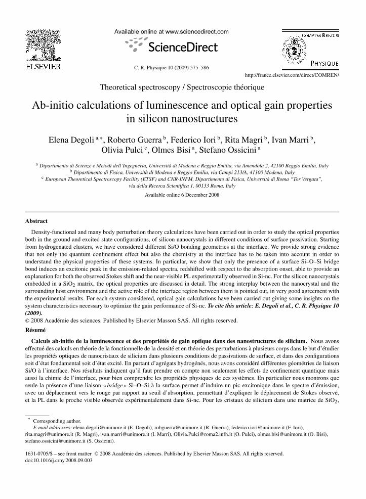
Optical gain spectra have been calculated for the Si10 clusters with the oxygen atom double bonded (see Fig. 4) andbridge bonded (see Fig. 5) at the cluster surface (we recall that gain calculation have been performed within a singleparticle approach and this means that absorption spectra of Fig. 3 cannot be compared with that of Figs. 4 and 5).Excited state geometry has been considered in order to take into account the structural relaxation due to populationinversion between band edges states. Four different electronic configurations have been considered in both cases:(i) the ground state configuration (top panel on the left), the population inversion between (ii) the (HOMO-1) andLUMO states (top panel on the right) (iii) the HOMO and LUMO states (bottom panel on the left) and (iv) the HOMOand (LUMO+1) states (bottom panel on the right). In each condition of population inversion new features, with respectto the absorption peaks in the ground state configuration, are present in the optical spectra in the low energy range dueto both intra- and inter-band transitions. Anyway, optical gain, i.e. negative absorption peaks, can be observed onlyfor population inversion between HOMO-LUMO and (HOMO-1)-LUMO states in both type of oxygen bond. On theother hand, the HOMO-(LUMO+1) transition is dark and the population inversion between these two states do notgives rise to gain peaks.
582 E. Degoli et al. / C. R. Physique 10 (2009) 575–586
Fig. 4. Imaginary part of the dielectric function for the Si10H14=O cluster in the ES geometry with four different electronic configurations. Toppanel: ground state configuration on the left, population inversion between the (HOMO-1) and LUMO states on the right. Bottom panel: populationinversion between the HOMO and LUMO states on the left and between the HOMO and (LUMO+1) on the right.
In the case of Si10H14=O whose energy gap in the ground state configuration is 0.74 eV the negative peaks are dueto the HOMO-LUMO transition in the case of HOMO-LUMO population inversion and to the (HOMO-1)-LUMOtransition when the inversion is between (HOMO-1) and LUMO states. For the Si10H14>O instead the gain in theHOMO-LUMO population inversion case is again due to the HOMO-LUMO transition while is due to the (HOMO-1)-HOMO intraband transition when the (HOMO-1) is depleted and the LUMO filled.
4. Silicon nanocrystals embedded in a SiO2 matrix
In this section our goal is to build up a simple model to study the properties of Si nanocrystals embedded in SiO2
matrix from a theoretical point of view [29]. To have a silicon skeleton with a crystalline behavior for simulating theSi-nc and the simplest Si–SiO2 interface, with the minimum number of dangling bonds or defects, we have considereda cubic cell (l = 14.32 Å) of SiO2 beta-cristobalite (BC) which has a diamond-like structure [30]. This cell is builtdoubling the unit cell of SiO2 BC along each Cartesian axis. Then we obtained a small cluster simply deleting someoxygen atoms of the SiO2 matrix and linking together the silicon atoms left with dangling bonds, as shown in Fig. 6.In this way we have built an initial supercell of 64 Si and 116 O atoms with 10 Si bonded together to form a smallcrystalline skeleton (Td interstitial symmetry) with a very highly strained bond length with respect to the bulk case:3.1 Å. We have performed a molecular dynamics simulation through a Car–Parrinello approach to fully relax thesystem. Fig. 6 shows the final relaxed supercell structure after the geometry optimization for the Si-nc (Si10) in SiO2.Looking at the cluster behavior we find that the skeleton is still crystalline-like (diamond) with a Si–Si bond lengthof 2.67 Å, that means a strain of 14% respect to the bulk case. This rearrangement causes a complex deformationof the SiO2 matrix around the cluster both in bond lengths and angles. Nevertheless the deformation does not affect

E. Degoli et al. / C. R. Physique 10 (2009) 575–586 583
Fig. 5. Imaginary part of the dielectric function for the Si10H14>O cluster in the ES geometry with four different electronic configurations. Toppanel: ground state configuration on the left, population inversion between the (HOMO-1) and LUMO states on the right. Bottom panel: populationinversion between the HOMO and LUMO states on the left and between the HOMO and (LUMO+1) on the right.
Fig. 6. Stick and ball pictures of the final optimized structure of Si10 in SiO2. The dark gray spheres represent O atoms, light gray Si and white theSi atoms of the nanocrystal.
the all SiO2 matrix. It is actually possible to find still a good BC crystalline structure, in terms of angles and bond-length, at a distance from the cluster’s atoms of 0.8–0.9 nm. This means that the cluster is surrounded by a cap-shellof stressed SiO2 BC with a thickness of about 1 nm which progressively goes towards a pure crystalline BC. Despitethe simplicity of the model, this picture is in close agreement with what emerges from energy-filtered transmissionelectron microscopy (EFTMEM) and X-ray measurements on Si nanocrystals in SiO2 samples produced by PECVD

584 E. Degoli et al. / C. R. Physique 10 (2009) 575–586
Fig. 7. Band structure along high symmetry points of the BZ for the Si10 cluster in SiO2 (left panel) compared with the band structure of beta-cristobalite bulk (right panel) and the energy levels at the Γ point for the isolated Si10H16 cluster (central panel).
Fig. 8. Imaginary part of the dielectric function for the Si10 cluster inBC matrix (dashed line) compared with that of isolated, hydrogenatedSi10 cluster (dotted line) and of the beta-cristobalite bulk (solid line).
Fig. 9. The optical gain spectrum for the Si10 nanocluster embeddedin a SiO2 matrix in the low energy region.
[31,32]. This view is also supported by the analysis of the electronic properties2 reported in Fig. 7. The calculated DFTEg for the cluster in the matrix is 1.48 eV, that must be compared with the value of 4.58 eV for the Eg of BC SiO2(bulk).3 The strong reduction is originated by the presence, at the valence and conduction band edges, of confined,flat, states completely related to the Si10–SiO2 interface. Actually nor the isolated, H-passivated cluster (see Fig. 7,central panel), neither the pure SiO2 matrix (see Fig. 7, right panel) show these states, whereas deep inside the valenceand conduction bands the more k-dispersed states related to the SiO2 matrix are still present. These interface-relatedstates originate strong absorption features in the optical region as witnessed from Fig. 8 where absorption spectra ofthe isolated Si10 cluster, of the pure matrix and of the composed system are reported. These features are entirely new,they do not exist for the isolated cluster or for the pure matrix, and so have to be due to the nature of the interfaceregion. The origin of the PL observed in the red optical region for Si-nc immersed in a SiO2 matrix can than be foundin the properties of this interface. Our result concerning the role of both Si-nc and the interface Si–O region withrespect to the absorption process is in close agreement with the X-ray absorption fine structure measurements [31]that indicate the presence of an intermediate region between the Si-nc and the SiO2 matrix about 1 nm thick thatparticipates in the light emission process. Very recently we have also calculated, for the first time, the gain spectra (asdescribed in Section 2) for this small Si-nc in the beta-cristobalite matrix,4 finding the presence of negative features inthe low energy region of the spectrum for transitions related to electronic states centered on the nanocluster. Actually,the three negative peaks shown in Fig. 9 are really near one to each other (the region that include the three peaks isabout 0.10 eV wide) and correspond to the HOMO-LUMO transition at different k-points in the reciprocal space.
2 The electronic and optical properties have been calculated through a pseudopotential approach using norm conserving pseudopotential with anenergy cutoff of 30 Ry.
3 The numerical values differences with respect to the previously published paper [29] are due to the different computational code used.4 For the optical gain spectrum calculation an energy cutoff of 25 Ry has been used.

E. Degoli et al. / C. R. Physique 10 (2009) 575–586 585
5. Conclusions
In conclusion, we have performed a theoretical study of the properties of Si nanocrystals. We have demonstrated,by first-principle calculations also beyond the single particle approach, that the optical properties of Si nanocrystalsstrongly depend on the different passivation regimes. Starting from hydrogen-covered Si nanoparticles we have shownthat:
(i) Optical properties calculations concerning the role of oxidation performed fully including excitonic effects sug-gests, if compared with experimental data, that only the presence of a Si–O–Si bridge bond at the surface ofSi-nc can explain the nature of luminescence in these systems: only in this case, in the many-body calculations,the presence of an excitonic peak in the emission-related spectra, redshifted with respect to the absorption onset,provide an explanation for both the observed SS and the near-visible PL in Si-nc.
(ii) When Si nanocrystals are embedded in a SiO2 matrix new electronic states originate within the silica band gapand both the Si atoms in the nanocrystals and the O atoms at the interface play a role in the optical properties.This theoretical analysis clearly point out the important role played not only by the Si nanocrystals but also bya modified silica capping region in determining the optoelectronic properties of the system. Our results help toclarify the experimental outcomes regarding the optical properties of Si-nc dispersed in SiO2 [31,33].
For each system considered optical gain calculations have been performed within a single particle scheme. The ob-tained results could give some insight concerning the best nanoclusters characteristics and the energy levels importantin order to observe optical gain.
Acknowledgements
We would like to acknowledge Domenico Ninno, Giovanni Cantele, Eleonora Luppi and Marcello Luppi, fortheir contribution to the realization of this paper. All the calculations have been performed at CINECA-Bologna (weacknowledge the “Iniziativa calcolo parallelo” of CNR-INFM) and CICAIA-Modena advanced computing facilities.
References
[1] S. Ossicini, L. Pavesi, F. Priolo, Light Emitting Silicon for Microphotonics, Springer Tracts on Modern Physics, vol. 194, Springer-Verlag,Berlin, 2003.
[2] Bisi, S. Ossicini, L. Pavesi, Surf. Sci. Rep. 38 (2000) 5.[3] G. Franzó, A. Irrera, E.C. Moreira, M. Miritello, F. Iacona, D. Sanfilippo, G. Di Stefano, P.G. Falica, F. Priolo, Appl. Phys. A 77 (2003) 57.[4] R.J. Walters, G.I. Bourianoff, H.A. Atwater, Nature Materials 4 (2005) 143.[5] L. Pavesi, L. Dal Negro, C. Mazzoleni, G. Franzó, F. Priolo, Nature (London) 408 (2000) 440.[6] L. Khriachtchev, M. Rasanen, S. Novikov, J. Sinkkonen, Appl. Phys. Lett. 79 (2001) 1249.[7] L. Dal Negro, M. Cazzanelli, L. Pavesi, S. Ossicini, D. Pacifici, G. Franzó, F. Priolo, F. Iacona, Appl. Phys. Lett. 82 (2003) 4636.[8] J. Ruan, P.M. Fauchet, L. Dal Negro, M. Cazzanelli, L. Pavesi, Appl. Phys. Lett. 83 (2003) 5479.[9] M. Cazzanelli, D. Kovalev, L. Dal Negro, Z. Gaburro, L. Pavesi, Phys. Rev. Lett. 93 (2004) 207042.
[10] K. Luterová, K. Dohnalová, V. S̆ervc̆ek, I. Pelant, J.-P. Likforman, O. Cérgut, P. Gilliot, B. Hönerlage, Appl. Phys. Lett. 87 (2004) 3280.[11] L.D. Negro, S. Gaponenko, L. Pavesi (Eds.), Towards the First Silicon Laser, Nato Science Series, vol. 93, Kluwer Academic Publishers,
Dordrecht, 2003.[12] S. Ossicini, C. Arcangeli, O. Bisi, E. Degoli, M. Luppi, R. Magri, L. Dal Negro, L. Pavesi, Gain theory and models in silicon nanostructures, in:
L. Dal Negro, S. Gaponenko, L. Pavesi (Eds.), Towards the First Silicon Laser, in: Nato Science Series, vol. 93, Kluwer Academic Publishers,Dordrecht, 2003, pp. 271–290.
[13] L. Dal Negro, M. Cazzanelli, Z. Gaburro, P. Bettotti, L. Pavesi, F. Priolo, G. Franzò, D. Pacifici, F. Iacona, Stimulated emission in siliconnanocrystals: Gain measurement and rate equation modeling, in: L. Pavesi, S. Gaponenko, L. Dal Negro (Eds.), Towards the First SiliconLaser, in: NATO Science Series, vol. 93, Kluwer Academic Publishers, Dordrecht, 2003, pp. 145–164.
[14] M.V. Wolkin, J. Jorne, P.M. Fauchet, G. Allan, C. Delerue, Phys. Rev. Lett. 82 (1999) 197.[15] A. Puzder, A.J. Williamson, J.C. Grossman, G. Galli, Phys. Rev. Lett. 88 (2002) 097401.[16] M. Luppi, S. Ossicini, J. Appl. Phys. 94 (2003) 2130.[17] I. Vasiliev, J.R. Chelikowsky, R.M. Martin, Phys. Rev. B 65 (2002) 121302(R).[18] M. Gatti, G. Onida, Phys. Rev. B 72 (2005) 045442.[19] L. Ramos, J. Furthmüller, F. Bechstedt, Appl. Phys. Lett. 87 (2005) 143113.[20] O. Pulci, M. Marsili, E. Luppi, C. Hogan, V. Garbuio, F. Sottile, R. Magri, R. Del Sole, Phys. Status Solidi B 242 (13) (2005) 2737–2750.

586 E. Degoli et al. / C. R. Physique 10 (2009) 575–586
[21] M. Palummo, M. Bruno, O. Pulci, E. Luppi, E. Degoli, S. Ossicini, R. Del Sole, Surf. Sci. 601 (13) (2007) 2696.[22] F. Bassani, G. Pastori Parravicini, Electronic States and Optical Transitions in Solids, Pergamon Press, New York, 1975.[23] E. Luppi, E. Degoli, G. Cantele, S. Ossicini, R. Magri, D. Ninno, O. Bisi, O. Pulci, G. Onida, M. Gatti, A. Incze, R. Del Sole, Opt. Mater. 27
(2005) 1008.[24] A. Puzder, A.J. Williamson, J.C. Grossman, G. Galli, J. Am. Chem. Soc. 125 (2003) 2786.[25] A. Franceschetti, S.T. Pantelides, Phys. Rev. B 68 (2003) 033313.[26] E. Degoli, G. Cantele, E. Luppi, R. Magri, D. Ninno, O. Bisi, S. Ossicini, Phys. Rev. B 69 (2004) 155411.[27] S. Baroni, A. Dal Corso, S. de Gironcoli, P. Giannozzi, C. Cavazzoni, G. Ballabio, S. Scandolo, G. Chiarotti, P. Focher, A. Pasquarello,
K. Laasonen, A. Trave, R. Car, N. Marzari, A. Kokalj, The DFT calculations for oxidized clusters have been performed using the ESPRESSOpackage, http://www.pwscf.org/.
[28] Z. Ma, X. Liao, G. Kong, J. Chu, Appl. Phys. Lett. 75 (1999) 1857.[29] M. Luppi, S. Ossicini, Phys. Rev. B 71 (2005) 035340.[30] H. Kageshima, K. Shiraishi, in: M. Scheffler, R. Zimmermann (Eds.), Proc. 23rd Int. Conf. Phys. Semicon., World Scientific, Singapore, 1996,
p. 903.[31] N. Daldosso, M. Luppi, S. Ossicini, E. Degoli, R. Magri, G. Dalba, P. Fornasini, R. Grisenti, F. Rocca, L. Pavesi, S. Boninelli, F. Priolo,
C. Spinella, F. Iacona, Phys. Rev. B 68 (2003) 085327.[32] T. Takagahara, K. Takeda, Phys. Rev. B 46 (15) (1992) 578.[33] N. Daldosso, G. Dalba, R. Grisenti, L.D. Negro, L. Pavesi, F. Rocca, F. Priolo, D. Pacifici, G. Franzò, F. Iacona, Physica E (Amsterdam) 16
(2003) 429.