Propriétés électriques des nanostructures π-conjuguées
221
HAL Id: tel-00836614 https://tel.archives-ouvertes.fr/tel-00836614 Submitted on 21 Jun 2013 HAL is a multi-disciplinary open access archive for the deposit and dissemination of sci- entific research documents, whether they are pub- lished or not. The documents may come from teaching and research institutions in France or abroad, or from public or private research centers. L’archive ouverte pluridisciplinaire HAL, est destinée au dépôt et à la diffusion de documents scientifiques de niveau recherche, publiés ou non, émanant des établissements d’enseignement et de recherche français ou étrangers, des laboratoires publics ou privés. Propriétés électriques des nanostructures π -conjuguées Appan Merari Masillamani To cite this version: Appan Merari Masillamani. Propriétés électriques des nanostructures π-conjuguées. Other. Université de Strasbourg, 2013. English. NNT : 2013STRAF009. tel-00836614
-
Upload
khangminh22 -
Category
Documents
-
view
1 -
download
0
Transcript of Propriétés électriques des nanostructures π-conjuguées

HAL Id: tel-00836614https://tel.archives-ouvertes.fr/tel-00836614
Submitted on 21 Jun 2013
HAL is a multi-disciplinary open accessarchive for the deposit and dissemination of sci-entific research documents, whether they are pub-lished or not. The documents may come fromteaching and research institutions in France orabroad, or from public or private research centers.
L’archive ouverte pluridisciplinaire HAL, estdestinée au dépôt et à la diffusion de documentsscientifiques de niveau recherche, publiés ou non,émanant des établissements d’enseignement et derecherche français ou étrangers, des laboratoirespublics ou privés.
Propriétés électriques des nanostructures π-conjuguéesAppan Merari Masillamani
To cite this version:Appan Merari Masillamani. Propriétés électriques des nanostructures π-conjuguées. Other. Universitéde Strasbourg, 2013. English. NNT : 2013STRAF009. tel-00836614

UNIVERSITÉ DE STRASBOURG
ÉCOLE DOCTORALE DES SCIENCES CHIMIQUES
UMR 7006 - Institut de Science et d'Ingénierie Supramoléculaires (I.S.I.S.)
THÈSE présentée par
Appan Merari MASILLAMANI
soutenue le : 04 Février 2013
pour obtenir le grade de
Docteur de l’université de Strasbourg
Discipline / Spécialité : Chimie Physique
Propriétés électriques des nanostructures π-conjugués
THÈSE dirigée par :
M. SAMORI Paolo Professeur, Université de Strasbourg
RAPPORTEURS :
Dr. VUILLAUME Dominique Research Director at CNRS, Institut
d’Electronique de Microélectronique et de
Nanotechnologie, Villeneuve
Dr. SIMON Laurent Research Director at CNRS, Institut de Sciences
des Matériaux de Mulhouse, Mulhouse
MEMBRES DU JURY :
Prof. DOUDIN Bernard Professeur, Université de Strasbourg –
Rapporteur interne
Dr. VUILLAUME Dominique Director at CNRS - Rapporteur externe
Dr. SIMON Laurent Director at CNRS - Rapporteur externe
Prof. SAMORI Paolo Professeur, Université de Strasbourg – Directeur
de thèse


Preface
I started research in the field organic based electronics rather by accident when I was
completing my Master’s degree courses in Sweden in the end of 2005. Prior to that I was
trained as an electronics and communication engineer, mostly working with inorganic
electronic devices, microprocessor circuits and communication systems during our
laboratory assignments. As a part of the master’s degree we had to complete a six month
project in either an industrial organization or an academic institution. I chose to go to the
University College London, UK in 2006 where I carried out research to understand the
properties of charge transport in various organic transistors by electrical characterization.
Furthermore, during the course of this project I developed the platform for testing these
devices. I had been out of material science research for the next three years. One thing led
to another and in the spring of 2010 I started my doctorate in the Nanochemistry
laboratory, based at the Institut de Science et d'Ingénierie Supramoléculaires of Université
de Strasbourg, France. During the course of my PhD I worked in completely diverse
aspects to address physical and chemical such as structural and electronic properties of
organic semiconductors and small molecule based devices. I would honestly say that many
a times it seemed impossible to reach a goal like making an experiment work or finding a
solution to assemble and improve the setup of an instrument, but I always had a strong
inherent belief within myself that it could be done. So I persevered, tried harder, thought
innovatively out the box, repeated experiments, even failed sometimes, but every time I
was learning and gradually improving my knowledge how to make a system work better
than the previous trial. Eventually as I pen down these last few sentences as my thesis is
coming to an end, I can look back and boldly state that I gave it my best shot and I really
cherished the challenge.
Appan Merari Masillamani
Strasbourg, 11/01/2013


Statement of work
I Appan Merari Masillamani do solemnly state that the works carried out during my thesis
are of my undertaking, unless otherwise explicitly mentioned.
The cyclic voltammogram for the biphenyl thiol SAMs and many initial experiments with
the mercury drop junctions were jointly performed with Dr. Núria Crivillers. Dr. Emanuele
Orgiu prepared the P3HT:PTTP and P3HT/DAE blend transistors and performed the
ionization energy characterization of P3HT:PTTP films. Dr. Jörn-Oliver Vogel performed
the morphological characterization with atomic force microscopy of P3HT:PTTP blend
films.
Dr. Florian Dötz synthesized the PTTP small molecules. Dr. Jürgen Rotzler and Mr. David
Bossert from the University of Basel synthesized the biphenyl thiol derivatives. Dr.
Federica Reinders synthesized the fluorinated azobenzene derivatives. Prof. Jean-Charles
Ribierre provided the quinoidal oligomer semiconductor.
Dr. Ramakrishnappa Thippeswamy and Prof. Michael Zharnikov carried out the X-ray
absorption characteristics of the biphenyl thiol SAMs on gold. Mr. Adam Kiersnowski and
Dr. Wojtek Pisula performed the microstructure characterization of the P3HT:PTTP blend
films.
I carried out theoretical simulations jointly with Mr. Silvio Osella to study the work
function change induced by fluorinated azobenzene self-assembled monolayers on gold
and started the initial transmission studies through single azobenzene molecule linked to
gold electrodes. Later on Mr. Osella extended the work to different azobenzene derivatives.


To
Ashok, Geetha and Linda


The essence of the beautiful is unity in variety.
-Felix Mendelssohn (1809-1847), Composer


I
Appan Merari MASILLAMANI
Propriétés électriques des nanostructures π-conjuguées
Résumé
Mots-clés: molécules π-conjugués, transistors organiques, monocouche auto assemblée, transport de charge
Cette thèse traite de l'étude du transport de charge à travers les semi-conducteurs organiques au sein de
transistors à effet de champ organiques (OFET). Une grande attention a été accordée aux interfaces dans les
OFET dont les propriétés ont été accordées pour moduler la réponse transistor. La stabilité de l'appareil en état
de commutation et le mécanisme régissant l'injection de charges ont été étudiés systématiquement. Le transport
de charge au niveau fondamental à travers les monocouches auto-assemblées comprenant une grande variété
des molécules π-conjuguées a été étudié.
Dans cette thèse, le processus de transport de charge et différents paramètres affectant ce phénomène sont
examinées en détail par la fabrication et la caractérisation de trois terminaux basés sur des architectures OFET
et deux dispositifs de jonctions terminales constituées d’une couche mono-moléculaire sur la surface de
l'électrode métallique.
Parmi les différents aspects relatifs à l'injection de charge dans des transistors organiques macroscopiques à
couches minces, un accent particulier a été mis sur l'interface1 de l’engineering
1 en réglant (i) le diélectrique /
l’interface semi-conducteur, et (ii) l'électrode en métal / le semi-conducteur. Pour explorer les aspects régissant
le transport de charge dans le canal de l'appareil, nous avons étudié la propriété de (iii) la mobilité intrinsèque
dans la semi-conductivité des matériaux et (iv) l'utilisation de mélanges dans la couche active du dispositif.
A l’échelle nanométrique, le transport de charge, grâce à une mono-couche moléculaire chimisorbé sur des
électrodes métalliques, a été étudié. L'auto-assemblage avec des groupes terminaux thiol sur des électrodes
d’or2 a été exploité pour former une monocouche.
2 Pour effectuer la caractérisation électrique sur la mono
couche auto-assemblée (SAM), nous avons construit un système de configuration comprenant des alliages
eutectiques de gallium et d'indium liquide métallique (GainE) comme électrode.
1 Le terme « interface » se réfère à la limite entre le semi-conducteur organique avec couche isolante ou avec des électrodes
d'injection de charge ou inter-moléculaires frontières. 2 Thiol à base de petites molécules en raison de son affinité chimique s’adsorbe sur la surface d'or par auto-assemblage processus et
la structure qui est formée est nommé comme monocouche auto-assemblée (SAM).

II
Avant l’utilisation du GainE comme électrode supérieure, Hg(goutte) a été utilisé comme électrode de test pour
effectuer la caractérisation électrique sur les SAMs. La raison du choix d’utilisation du GainE est explicitée
dans ma thèse.
Nous avons entrepris les méthodes suivantes pour moduler les propriétés qui affectent le transport de charge
dans les OFET:
1) L'interface semi-conducteur / diélectrique: Dans ce travail nous avons étudié l'influence que le
changement dans la masse moléculaire de polymères diélectriques pourrait avoir sur les transistors. Le
transport de charge dans les transistors organiques se produit à l'interface.3 Pour régler les propriétés de
surface du diélectrique en contact avec le semiconducteur4 on utilise deux diélectriques polymériques avec des
constantes diélectriques différentes. Les effets de commutation de stabilité et de l'hystérésis ont été observés.
2) L'interface métal / semi-conducteurs: Pour mieux comprendre les propriétés d'injection de charge de
SAM biphényle thiols chimisorbées sur l’électrode source drain du transistor, nous avons fabriqué et
caractérisé une famille de biphényles dérivés thiols avec un degré variable de torsion dans son squelette
moléculaire. Des paramètres tels que la modification de la fonction de travail,5 les électrodes de mouillage et
son effet correspondant à la mobilité de charge et tension dans le transistor à base de poly (3 hexylthiophène)
ont été étudiés.
Nous avons étudié le transport de charge grâce à des thiols fluorés azobenzène avec des substitutions mono et
biphényle auto-assemblés sur électrode d'or. Ces molécules ont été synthétisées par le groupe du professeur
Marcel Mayor. Le transport de charge à travers les deux formes isomères trans et cis, a été étudié. Pour le
biphényle substitué azobenzène fluoré, le mouillage de surface et les variations de la fonction de travail de
l'électrode modifiée avec le SAM ont été évalués par différentes techniques.
3) Transport de charge en vrac semi-conducteur intrinsèque: pour rechercher la mobilité des porteurs
intrinsèques pour OFET basé sur thiophène quinoidal possédant une nature amorphe dans la masse du film,
nous avons effectué une caractérisation dans un cryostat. De précieux renseignements sur le mécanisme de
piégeage possible et l'énergie d'activation correspondant à la fois à des systèmes de types p et n ont été acquis.
Une autre étude a également été réalisée pour enregistrer l'énergie d'activation d'un transistor avec un mélange
à deux composants de la couche de transport de charge dans l'appareil.
4) Mélanges dans la couche active: Pour moduler la mobilité des trous porteurs de charge des transistors,
nous avons employé la technique de mélanger une petite molécule avec un polymère conjugué. Les effets de la
séparation de phase et de l'orientation moléculaire sur le mélange et son influence sur le transport de charge
sont détaillés dans cette étude.
III
L'interface semi-conducteur / diélectrique
Les chercheurs ont essayé de remplacer le dioxyde de silicium avec des diélectriques polymères par des OFET
au courant du siècle.6 Les principaux avantages de l'utilisation de diélectriques polymères sont leur
processabilité dans la solution, la flexibilité, la facilité de dépôt sur des substrats et programmabilité des
propriétés de surface. Jusqu'à présent, pour notre projet nous avons utilisé deux diélectriques avec des
constantes diélectriques différentes allant de la plus petite à la plus grande masse moléculaire, en combinaison
avec un polymère fluoré conjugué dont les caractéristiques de transport de charge ambipolaire ont été
démontrées. Tous les diélectriques polymériques et semi-conducteurs utilisés ont été acquis auprès de sources
commerciales. Le rôle de l'énergie de surface diélectrique et la modification de polarité de surface lors d'un
changement du poids moléculaire et son influence sur les performances du dispositif ont été étudiés. La
question de la stabilité de commutation l’Etat OFF à ON et vice versa a été examinée pour toutes les
configurations diélectriques / semi-conducteur, car cela donne des informations cruciales quant à la fiabilité de
l'appareil sur un fonctionnement prolongé.
L'interface métal / semi-conducteurs
Dans le cas de la modulation d'injection de charges avec les électrodes des transistors à couches minces au
moyen de la famille des SAM biphényles nous avons collaboré avec le groupe du prof. Marcel Mayor de
l'Université de Bâle (Suisse) qui nous a fourni ces molécules. Pour avoir un aperçu de la densité structurelle de
l’empilement moléculaire et de l'angle d'inclinaison des molécules sur la surface de l'électrode en or, nous
avons collaboré avec le groupe du prof. Michael Zharnikov de l'Universität Heidelberg (Allemagne) qui a
effectué les travaux de spectroscopie d’absorption des rayons X (NEXAFS) et de spectroscopie de
photoélectrons (XPS). Une série de mesures ont été faites sur des OFET pour mieux comprendre l'injection de
charge électrique et le transport à travers les SAM, qui dépendent de l'ordre structurel, de l'épaisseur effective
et de l’angle d'inclinaison à la surface des électrodes. La modulation de la mobilités de trous d’électrons a été
atteinte sur l'intégration des SAM thiolés biphényle dans les électrodes OFET en raison de la modification de la
fonction de travail des électrodes source-drain.7,8
Nous avons également effectué la caractérisation électrique sur des thiols fluorés azobenzène substitutés mono
ou biphényle auto-assemblés sur électrode d'or. La caractérisation électrique des SAM a été réalisée avec une
configuration développée spécialement en interne dans ce but. Nous avons peaufiné et amélioré la
configuration progressivement au cours du temps de du travail de doctorat afin d'améliorer la fiabilité et la
qualité des mesures. Nous avons testé notre configuration avec les systèmes déjà étudiés pour vérifier la
sensibilité de nos mesures avec les résultats publiés dans la littérature.

IV
Pour mieux comprendre comment la transmission à travers une seule molécule d'azobenzène est liée aux
changements des électrodes d'or nous avons réalisé une étude théorique avec nos collaborateurs à l'Université
de Mons (Belgique) projet de réseau SUPERIOR, avec notamment Silvio Osella et le Dr. Jérôme Cornil.
Transport de charge en vrac du semi-conducteur intrinsèque
Pour étudier la mobilité de la charge intrinsèque de transistors à base d’oligothiophène quinoidal sur la couche
active dans les OFET nous avons collaboré avec le groupe du prof. Jean-Charles Ribierre, Ewha Womans
University (Corée du Sud) qui nous a fourni ce composé. La caractérisation à des températures allant de 80 K à
300 K a été effectuée au moyen d'un cryostat configuré spécifiquement pour effectuer la caractérisation
électrique sur des OFET. Un porte-échantillon personnalisé avec les connexions électriques pour la même
caractérisation des OFET dans le cryostat a été construit. Le oligothiophène quinoidal, lors du dépôt, présente
la propriété de se comporter comme un matériau de transport de trous et d’électrons après réchauffement.9,10
Les énergies d'activation pour le cas particulier des modes de fonctionnement de type p et n ont été estimées.
Pour comprendre le rôle de la température dans le mécanisme de transport de charge par le biais d'un polymère
semi-conducteur avec un photochrome comme couche active du transistor, la caractérisation électrique de cet
OFET a été réalisée dans un cryostat. Les énergies d'activation ont été estimées pour les deux configurations
d’état (ouvert et fermé) de la molécule diaryléthène, photochromique mélangé à un semi-conducteur. Le
déséquilibre énergétique entre les niveaux d'énergie d'ionisation de poly (3 hexylthiophène) et diaryléthène
ouvert est beaucoup plus grand comparé au diaryléthène fermé. Par conséquent, les énergies d'activation
requises pour thermiquement activer le saut de charge devraient être différentes dans les deux cas.
Mélanges dans la couche active
Le projet sur les mélanges comme couche active d’OFET était un travail de collaboration avec les membres de
la ISOF-Consiglio Nazionale delle Ricerche (Italie) et BASF (Suisse) à partir desquels les phenylene–
thiophene–thiophene–phenylene (la petite molécule) ont été acquises. L’alliage de différents matériaux est
l'une des méthodes utilisées pour modifier les niveaux d'ionisation énergétiques de la plus grande partie de la
couche mince dans un transistor et donc la mobilité du porteur de charge.11
L’étude de la diffraction des rayons
X et la caractérisation grand angle de la diffusion des rayons X ont été effectuées à l'institut Max Planck de
recherche sur les polymères (Mainz). A partir de ces résultats le rôle de la petite molécule de polymère
d'emballage a été établi. On a effectué la qualification électrique complète de l’OFET qui a une couche active
différente selon la quantité de petite molécule mélangée au polymère semi-conducteur. La caractérisation
morphologique a été faite à l’aide d’un microscope à force atomique (AFM).

V
Résumé
Une étude approfondie a été réalisée au cours de mon travail de thèse sur les différents facteurs régissant le
transport de charge dans les molécules organiques. Nous nous sommes concentrés sur l'optimisation des
propriétés des interfaces dans le transistor à couche mince. L'influence de l'énergie de surface, de la polarité et
du mouillage des polymères diélectriques ou semi-conducteurs sur la stabilité et la fiabilité des OFET « top
gate » a été étudié en détail. Le rôle de l'injection de charges variable en raison de différentes molécules de
thiol chimisorbées sur le transistor entrainant la modification des niveaux énergétiques des électrodes de
« source » et « drain » a été étudié. Sur un plan fondamental le transport de charge intrinsèque à travers le
semi-conducteur chauffé après déposition a été étudié. L'effet du mélange entre une petite molécule
photochrome dans ses deux états bistables avec un semi-conducteur polymère sur le transport de charge a été
étudié au moyen de caractérisation électrique thermo-dépendante. Nous avons étudié en détail comment les
propriétés structurelles affectent la fonction du transport de charge pour des molécules telles que l'azobenzène
fluoré et les biphényle thiolates chimisorbés sur des électrodes en or.
Ces résultats fournissent des indices essentiels pour la conception de transistors avec un bon contrôle de
l'injection de charge à partir d'électrodes. Ils mettent également en évidence le fait que ces approches de
fabrication entraînent une baisse de coût et que le post-traitement des dispositifs peut être amélioré de manière
significative sans l’utilisation de techniques onéreuses.
VI
Références
1 Don Park, Y., Lim, J. A., Lee, H. S. & Cho, K. Interface engineering in organic transistors. Mater.
Today 10, 46-54, (2007).
2 Poirier, G. & Pylant, E. The self-assembly mechanism of alkanethiols on Au (111). Science 272, 1145-
1148 (1996).
3 Dodabalapur, A., Torsi, L. & Katz, H. E. Organic Transistors: Two-Dimensional Transport and
Improved Electrical Characteristics. Science 268, 270-271, (1995).
4 Veres, J., Ogier, S., Lloyd, G. & De Leeuw, D. Gate insulators in organic field-effect transistors. Chem.
Mater. 16, 4543-4555 (2004).
5 Heimel, G., Romaner, L., Zojer, E. & Bredas, J. L. The interface energetics of self-assembled
monolayers on metals. Acc. Chem. Res. 41, 721-729 (2008).
6 Facchetti, A., Yoon, M. H. & Marks, T. J. Gate dielectrics for organic field‐effect transistors: new
opportunities for organic electronics. Adv. Mater. 17, 1705-1725 (2005).
7 Stoliar, P. et al. Charge injection across self-assembly monolayers in organic field-effect transistors:
Odd-even effects. J. Am. Chem. Soc. 129, 6477-6484 (2007).
8 Boudinet, D. et al. Modification of gold source and drain electrodes by self-assembled monolayer in
staggered n-and p-channel organic thin film transistors. Org. Electron. 11, 227-237 (2010).
9 Ribierre, J. C. et al. Direct Laser Writing of Complementary Logic Gates and Lateral p–n Diodes in a
Solution-Processible Monolithic Organic Semiconductor. Adv. Mater. 22, 1722-1726, (2010).
10 Ribierre, J.-C. et al. Reversible Conversion of the Majority Carrier Type in Solution-Processed
Ambipolar Quinoidal Oligothiophene Thin Films. Adv. Mater. 22, 4044-4048, (2010).
11 Meijer, E. et al. Solution-processed ambipolar organic field-effect transistors and inverters. Nat. Mater.
2, 678-682 (2003).

VII
Résumé en anglais (Abstract in English)
Keywords: π-conjugated molecules, organic transistors, self-assembled monolayers, charge transport
This thesis deals with the study of charge transport through organic semiconductors incorporated in Organic
Field-Effect Transistors (OFETs). Great attention is given to the interfaces in the OFETs and the properties of
which were tuned to modulate transistor response. The stability of the device under switching states and the
mechanism governing charge injection were studied systematically. In a fundamental level the charge transport
through self-assembled monolayers comprising of variety of π-conjugated molecules were investigated.
In this thesis the charge transport process and different parameters affecting this phenomenon are investigated
in detail by fabrication and characterization of three terminal devices based on OFET architectures and two
terminal devices consisting junctions incorporating mono-molecular layer on surface of metal electrode.
Among the different aspects governing the charge injection in macroscopic organic thin film transistors
particular emphasis was given to the interface3 engineering
1 by tuning the (i) Dielectric/semiconductor
interface, and (ii) Metal electrode/semiconductor. To explore aspects governing charge transport within the
channel of the device we investigated the property of (iii) semiconductor intrinsic mobility and (iv) usage of
blends in the active layer of the transistor.
On the nanoscale the charge transport through a mono molecular layer chemisorbed onto metal electrodes was
investigated. The self-assembly of thiol molecules on gold electrodes4 was exploited to form monolayer.
2 To
perform electrical characterization on self-assembled monolayer (SAM) a custom in-house setup comprising of
eutectic alloy of liquid metallic gallium indium (GaInE) probe electrode was built. Prior to the using GaIn
E as
the top electrode Hg-drop was employed as the probe electrode for performing electrical characterization on
SAMs. The reasoning for preference of the GaInE is detailed in the methods section.
We undertook the following routes to modulate the properties affecting the charge transport in the OFETs:
1) Semiconductor/dielectric interface: In this work we investigated the influence which the change in the
molecular weight of polymeric dielectrics might have in top-gate bottom-contact transistors. The charge
transport in organic transistors occurs at the semiconductor/dielectric interface.3
3 The term interface refers to the boundary between organic semiconductor with insulator layer or with charge injection electrodes or
inter-molecular borders. 4 Thiol based small molecules due to its chemical affinity get adsorbed onto the surface of gold by self-assembly process and the
structure which is formed is termed as self-assembled monolayer (SAM).

VIII
To tune the surface properties of the dielectric in contact with the semiconductor4 we used two dielectrics with
different dielectric constants. The switching stability and hysteresis effects were examined.
2) Metal/Semiconductor interface: To gain insight into the charge injection properties of biphenyl thiol
SAMs chemisorbed on source-drain electrodes of the transistor we fabricated and characterized a family of
biphenyl thiol derivatives with a varying degree of torsion in its molecular backbone. Parameters such as work
function modification,5 wettability of the electrodes and their corresponding effect in charge mobility and
threshold voltage of bottom-gate bottom–contact transistors based on poly(3 hexylthiophene) were studied. We
studied the charge transport through fluorinated azobenzene thiols with mono and biphenyl substitutions self-
assembled on gold electrodes. These molecules were synthesized by the group of Prof. Marcel Mayor. Charge
transport through the two forms trans and cis isomers were studied. For fluorinated azobenzene substituted
biphenyl, the surface wettability and changes in the work function of the electrode modified with the SAM
were evaluated by different techniques.
3) Semiconductor bulk intrinsic transport: For investigating the intrinsic carrier mobility for OFETs based
on quinoidal thiophene which has an amorphous nature in the bulk of the film we performed electrical
characterization in a cryostat. Valuable insight into the possible trapping mechanism and the respective
activation energy for both p and n-type systems was acquired. A separate study was also carried out to record
the activation energy of a transistor with a bicomponent mixture as the charge transport layer in the device.
4) Blends in the active layer: To modulate the charge carrier hole mobility of transistors we followed the
approach to blend a small molecule with conjugated polymer. The effects of phase separation and molecular
orientation upon blending and its influence on the charge transport are detailed in this study.
Semiconductor/dielectric interface
Researchers have been trying to replace silicon dioxide with polymeric dielectrics over in OFETs at the turn of
the century.6 The major advantages of using polymeric dielectrics are their solution processability, flexibility
and ease of deposition onto substrates. Hitherto for our project we employed two dielectrics with different
dielectric constants spanning from a lower to high molecular weights in combination with a conjugated
fluorinated polymer which had been shown to exhibit ambipolar charge transport characteristics. All the
polymeric dielectrics and semiconductor used were acquired from commercial sources. This was an intra-team
project and a better part of this undertaking was particularly challenging, especially to attain the necessary
parameters to successfully fabricate and characterize the devices without impediments resulting in failed
devices was quite a thought provoking and exploratory task. The role of dielectric surface energy and surface
polarity modification upon changing the molecular weight and its influence on the device performance were
investigated.

IX
The issue of switching stability from off to on state and vice versa was examined for all
dielectric/semiconductor configurations, since this gives crucial information regarding the reliability of the
device on prolonged operation.
Metal/Semiconductor interface
In the case of the charge injection modulation with electrodes of the thin-film transistors by means of biphenyl
family of SAMs we collaborated with the group of prof. Marcel Mayor from University of Basel (Switzerland)
who provided us with these molecules. To gain insight into the structural order, molecular packing density and
tilt angle of the molecules on the surface of the gold electrode we collaborated with the group of prof. Michael
Zharnikov from Universität Heidelberg (Germany) who conducted the near-edge X-ray absorption
spectroscopy (NEXAFS) and X-ray photoelectron spectroscopy (XPS) measurements. A series of OFET
measurements were undertaken to shed light upon the charge injection and the transport across the SAMs,
which was found to be depend on the structural order, effective thickness and tilt angle on the surface of the
electrodes. The corresponding modulation of hole mobilities were achieved upon integration of the thiolated
biphenyl SAMs in OFET electrodes due to the work function modification of the source-drain electrodes.7,8
We also performed the electrical characterization for SAMs of fluorinated azobenzene thiols with mono and
substitutions biphenyl on gold electrodes. Electrical characterization of SAM was performed with a specially
developed setup. We have refined and improved gradually during the course of time during my doctoral work
to improve the reliability and integrity measures. We tested our setup with the systems already studied to test
the sensitivity of our measurements with the results published in the literature.
To further understand how the transmission through a single azobenzene molecule linked to gold electrodes
changes we performed a theoretical study with our collaborators at the University of Mons (Belgium) network
project SUPERIOR in particular Silvio Osella and Dr. Jérôme Cornil.
Semiconductor bulk intrinsic transport
To study the intrinsic charge carrier mobility of transistors based on quinoidal oligothiophene as the active
layer in the OFETs we collaborated with the group of prof. Jean Charles Ribierre, Ewha Womans University
(South Korea) who provided us with this compound. The characterization at temperatures ranging from 80 K –
300 K was performed by means of a cryostat configured specifically to perform electrical characterization on
the OFETs. A customized sample holder along with the electrical connections for the same in the cryostat was
built for characterization of OFETs. The quinoidal oligothiophene exhibits the property to behave like a hole
and electron transporting material upon deposition and then post annealing respectively.9,10
The activating
energies for the individual case of p and n-type operational mode were estimated.

X
To understand the temperature dependent charge transport mechanism through a polymeric semiconductor-
photochromic small molecule blend as the active layer of the transistor, electrical characterization of this OFET
was performed in a cryostat. The activation energies were estimated for both the ring opened and closed state
of the photochromic diarylethene molecule blended with semiconductor respectively. The energetic mismatch
between the ionization energy levels of P3HT and diarylethene open is much greater compared to diarylethene
closed. Hence the activation energies required for thermally activated charge hopping is expected to be
different in the two cases.
Blends in the active layer
The project with blends as the active layer of OFETs was a collaborative work with members at the ISOF–
Consiglio Nazionale delle Ricerche (Italy) and BASF (Switzerland) from whom the compounds were acquired.
Blending different materials is one of methods used to modify the ionization energetic levels of the thin-film
bulk in a transistor and thereby the mobility of charge carriers.11
The X-ray diffraction and the wide angle X-
ray scattering characterization were carried out at the Max Planck institute for polymer research, Mainz from
which the role of small molecule-polymer packing was gathered. We performed the complete electrical
characterization of the blend OFETs which had different ratio of small molecule-polymer mix by volume as
the active layer of the transistor. The morphological characterization on the semiconductor film was performed
by means of atomic force microscope (AFM).
Summary
A comprehensive study was carried out on various factors governing the charge transport in π-conjugated
organic molecules during this thesis work. We focused on tuning the properties of the interfaces in the thin-
film transistor. The influence of surface energy, polarity, wettability of the polymeric dielectrics/semiconductor
on the stability and reliability for top gate OFETs interface were studied in detail. The role of variable charge
injection due to different thiol molecules chemisorbed on the transistor resulting in modification of the
energetic levels source and drain electrodes were investigated. On a fundamental level the intrinsic charge
transport through the semiconductor upon post annealing and as deposited was investigated. The effect of
blending photochromic small molecule in its two bistable states with a polymeric semiconductor on the charge
transport was studied by means of temperature dependent electrical characterization. We investigated in detail,
how the structural properties affect the function of the charge transport for molecules such as fluorinated
azobenzene and biphenyl thiolates chemisorbed onto gold electrodes.
These results provide vital clues for designing transistors with good control over charge injection from
electrodes and more crucially also highlights the fact that following lost-cost fabrication approaches without
expensive post-processing techniques the efficiency of the devices can be improved significantly.

XI
References
1 Don Park, Y., Lim, J. A., Lee, H. S. & Cho, K. Interface engineering in organic transistors. Mater.
Today 10, 46-54, (2007).
2 Poirier, G. & Pylant, E. The self-assembly mechanism of alkanethiols on Au (111). Science 272, 1145-
1148 (1996).
3 Dodabalapur, A., Torsi, L. & Katz, H. E. Organic Transistors: Two-Dimensional Transport and
Improved Electrical Characteristics. Science 268, 270-271, (1995).
4 Veres, J., Ogier, S., Lloyd, G. & De Leeuw, D. Gate insulators in organic field-effect transistors. Chem.
Mater. 16, 4543-4555 (2004).
5 Heimel, G., Romaner, L., Zojer, E. & Bredas, J. L. The interface energetics of self-assembled
monolayers on metals. Acc. Chem. Res. 41, 721-729 (2008).
6 Facchetti, A., Yoon, M. H. & Marks, T. J. Gate dielectrics for organic field‐effect transistors: new
opportunities for organic electronics. Adv. Mater. 17, 1705-1725 (2005).
7 Stoliar, P. et al. Charge injection across self-assembly monolayers in organic field-effect transistors:
Odd-even effects. J. Am. Chem. Soc. 129, 6477-6484 (2007).
8 Boudinet, D. et al. Modification of gold source and drain electrodes by self-assembled monolayer in
staggered n-and p-channel organic thin film transistors. Org. Electron. 11, 227-237 (2010).
9 Ribierre, J. C. et al. Direct Laser Writing of Complementary Logic Gates and Lateral p–n Diodes in a
Solution-Processible Monolithic Organic Semiconductor. Adv. Mater. 22, 1722-1726, (2010).
10 Ribierre, J.-C. et al. Reversible Conversion of the Majority Carrier Type in Solution-Processed
Ambipolar Quinoidal Oligothiophene Thin Films. Adv. Mater. 22, 4044-4048, (2010).
11 Meijer, E. et al. Solution-processed ambipolar organic field-effect transistors and inverters. Nat. Mater.
2, 678-682 (2003).


I
Contents
Résumé…………………………………………………………………………………………..VII
Abstract in English……………………………………………………………………………...XIII
1 Introduction ............................................................................................................................. 1
1.1 Organic electronics ............................................................................................................... 1
1.1.1 Scope.............................................................................................................................. 2
1.2 Molecular electronics............................................................................................................ 3
1.2.1 Prospects ........................................................................................................................ 4
1.3 References............................................................................................................................. 5
2 Charge Transport in organic semiconductors .......................................................................... 7
2.1 Introduction........................................................................................................................... 7
2.2 Energetic profile of organic semiconductors ........................................................................ 9
2.3 CHARGE TRANSPORT: Mechanisms and models .......................................................... 12
2.3.1 Multiple trapping and release ...................................................................................... 13
2.3.2 Gaussian disorder model.............................................................................................. 15
2.3.3 Polaron hopping model ................................................................................................ 17
2.3.4 Bipolaron model .......................................................................................................... 19
2.4 Organic Field-effect transistor ............................................................................................ 20
2.4.1 OFET-working principles ............................................................................................ 20
2.4.2 Transistor performance indicators ............................................................................... 23
2.5 References and notes .......................................................................................................... 27

II
3 Charge Transport in molecular junctions ................................................................................... 29
3.1 Introduction......................................................................................................................... 29
3.1.1 Molecular junctions - building blocks ......................................................................... 29
3.1.2 Metal-molecule-metal junctions .................................................................................. 30
3.1.3 Quantum tunneling ...................................................................................................... 32
3.1.4 References and notes ................................................................................................... 35
4 Methods and procedures ........................................................................................................ 37
4.1 OFET PREPARATION ...................................................................................................... 37
4.1.1 F8BT based OTFTs ..................................................................................................... 37
4.1.2 P3HT based OTFTs ..................................................................................................... 39
4.1.3 QQT(CN)4 based OFETs ............................................................................................ 39
4.1.4 P3HT, diarylethene blend OFETs................................................................................ 39
4.1.5 P3HT, PTTP blend OFETs .......................................................................................... 40
4.2 OFET CHARACTERIZATION TECHNIQUES ............................................................... 40
4.2.1 Electrical characterization inside glovebox ................................................................. 40
4.2.2 Electrical characterization in cryostat .......................................................................... 40
4.2.3 Work function of electrodes ........................................................................................ 43
4.2.4 Ionization energy of semiconductor film ..................................................................... 43
4.2.5 Morphological characterization ................................................................................... 44
4.2.6 Microstructural characterization of P3HT:PTTP blend films ..................................... 44
4.2.7 Surface wettability tests ............................................................................................... 44
4.2.8 UV/Vis spectroscopy on films ..................................................................................... 44
4.3 SAM PREPARATION ....................................................................................................... 45
4.4 SAM CHARACTERIZATION TECHNIQUES ................................................................ 46
4.4.1 Electrical characterization of SAMs ............................................................................ 47
4.4.2 Structural characterization of SAMs ........................................................................... 50
4.5 References........................................................................................................................... 51

III
5 Organic field-effect transistors .............................................................................................. 53
5.1 Dielectric molecular weight influence in ambipolar F8BT OFETs.................................... 53
5.1.1 Scope............................................................................................................................ 53
5.1.2 Dielectric surface properties ........................................................................................ 55
5.1.3 Morphological characterization ................................................................................... 58
5.1.4 Electrode-Semiconductor interfacial energetics .......................................................... 60
5.1.5 Standard OFET electrical characterization .................................................................. 62
5.1.6 Effect of gate bias dependent hysteresis in TFTs ........................................................ 67
5.1.7 TFT switching capacity and instability under dynamic bias stress influence ............. 72
5.1.8 Conclusions.................................................................................................................. 79
5.1.9 References.................................................................................................................... 80
5.2 Intrinsic charge transport in polymeric semiconductor/photochromic molecular blend
OFETs ....................................................................................................................................... 83
5.2.1 Motivation.................................................................................................................... 83
5.2.2 Results and discussions................................................................................................ 86
5.2.3 Conclusions.................................................................................................................. 94
5.2.4 References and notes ................................................................................................... 95
5.3 Activation energy of OFETs based on Quinoidal Oligothiophene derivative .................... 97
5.3.1 Scope............................................................................................................................ 97
5.3.2 Results and discussions................................................................................................ 98
5.3.3 Conclusions................................................................................................................ 107
5.3.4 References.................................................................................................................. 108
5.4 Improved field-effect mobility in a polymeric semiconductor/small molecular blend
transistors ................................................................................................................................ 109
5.4.1 Prospects .................................................................................................................... 109
5.4.2 Results and discussions.............................................................................................. 110
5.4.3 Conclusions................................................................................................................ 116
5.4.4 References.................................................................................................................. 117

IV
6 Charge transport through SAMs .......................................................................................... 119
6.1 Charge Injection and Transport through Biphenylthiol SAMs .................................... 119
6.1.1 Introduction ........................................................................................................... 119
6.1.2 SAM Packing Density and Orientation ................................................................. 122
6.1.3 Charge Transport through Biphenylthiol SAMs ................................................... 127
6.1.4 Biphenylthiol SAMs in OTFT electrodes ............................................................. 133
6.1.5 Discussions ........................................................................................................... 140
6.1.6 Conclusions ........................................................................................................... 144
6.1.7 References ............................................................................................................. 145
6.2 Comparative study of work function modification of Au electrodes by fluorinated
azobenzene .............................................................................................................................. 149
6.2.1 Motivation.................................................................................................................. 149
6.2.2 Results and discussions.............................................................................................. 150
6.2.3 Conclusions................................................................................................................ 157
6.2.4 References.................................................................................................................. 160
6.3 Charge transport through self-assembled monolayers of fluorinated azobenzene on Au
electrodes ................................................................................................................................. 161
6.3.1 Motivation.................................................................................................................. 161
6.3.2 Results and discussions.............................................................................................. 162
6.3.3 References.................................................................................................................. 173
6.4 Transmission studies through single molecule azobenzene derivatives linking gold
electrodes ................................................................................................................................. 175
6.4.1 Motivation.................................................................................................................. 175
6.4.2 Provisional results ...................................................................................................... 175

V
7 Epilogue ............................................................................................................................... 181
7.1 Conclusions and outlooks ................................................................................................. 181
7.2 General long-term perspectives and directives ................................................................. 183
Appendix………………………………………………………………………………………..185
List of publications....…………………………………………………………………………..189
Acknowledgements……………………………………………………………………………..191


Chapter 1: Introduction
Appan Merari Masillamani 1
No problem is too small or too trivial if we can really do something about it
– Richard Feynman (1918-1988), Physicist
1 Introduction
Electronics deals with the physics of movement of electrons in devices such as transistors, diodes
to perform functions such as transport and amplification of current, rectification, signal filtering
and processing etc. In modern times electronic components are ubiquitous in our daily lives
encompassing from small and simple pocket calculators, display panels to complex
supercomputers. In the infancy of the electronics industry inorganic systems, such as those based
on single crystals of silicon, were incorporated as active materials in the devices for transporting
the charge carriers. Traditionally doped silicon was used as the semiconducting material. In the
late 1970’s after the discovery of increase in electrical conductivity of carbon based
polyacetylene upon electrochemical doping,1 the possibility of using organic materials as active
layers was proposed. This eventually led to the incorporation of π-conjugated carbon based
compounds in electronic components, thus paving the way for a new branch called ‘organic
electronics’.
1.1 ORGANIC ELECTRONICS
In organic semiconductors the interaction between the molecules are of loosely bound nature,
typically of van der Waals forces which is different from their inorganic counterpart which has
strong covalent bond in their crystal lattice. Due to the variations in intramolecular bond strength
of organic compounds, the net charge is not uniformly localized (i.e., not delocalized) in the
molecule and mobility is lower compared to crystalline silicon. The charge transport rates in the
organic materials are greatly influenced by their structural ordering in the bulk of the thin film in
the device. The organic materials can be divided into two main categories (i) small molecules/
monomeric units, and (ii) polymers. besides the molecular weight and polydispersity the major
difference between the small molecules and polymers is the methods employed for deposition. In
the case of small molecules the deposition is predominantly performed via thermal evaporation,
while in polymers techniques such as drop casting, spin coating or ink-jet printing have been
employed owing to its solution processability.

Chapter 1: Introduction
Appan Merari Masillamani 2
1.1.1 Scope
π-conjugated carbon based materials comprise of a broad class of materials and primarily
provide some unique advantages2 such as:
Processability: Most of the polymeric semiconductors are soluble in solvents, thereby
facilitating the process of deposition over large-area substrates by means of simple techniques
like spin coating, printing etc. The deposition can be carried out at low, i.e., room temperatures;
this also reduces the fabrication cost.
Flexibility: The organic compounds can be deposited on flexible light weight plastic substrates,
greatly reducing the bulkiness of the device.
Cost effective fabrication: Since the deposition can be done in standard condition (ambient
pressure and temperature) without the need of working in ultra-high vacuum the fabrication cost
is much less.
Versatile: With the aid of synthesis, the electronic properties of these organic compounds can be
modified by adding suitable substitutions in the molecular structure.
Though there are many pros for carbon based organic materials to be integrated into electronic
components, still the switching speed are lower than that of state of the art inorganic electronics
technology. One of the challenges is to optimize conditions for deposition of the semiconductor
film to minimize disorders like grain boundaries and pin holes that are known to hamper the rate
of charge transport in the thin film. Some of the potential applications are organic thin film
transistors (OTFTs),3 organic photovoltaics (OPVs), bio-sensors and organic light-emitting
diodes (OLEDs).4,5
Recent research is focused on improving the mobility, stability, efficiency,
lowering power consumption and reliability of operation over extended period of time in organic
electronic devices, with the eventual goal to nearly match the performance of their inorganic
counterpart. Each of the aforementioned issues were addressed during my thesis and it is
organized as the following:
Chapter 2 and 3 introduces the reader to fundamental concepts of charge transport in organic
field-effect transistors and in metal-molecule-metal based junctions, respectively.

Chapter 1: Introduction
Appan Merari Masillamani 3
Chapter 4 contains the complete set experimental methods and procedures followed for each of
the projects.
Chapter 5 deals with the charge transport problem in OTFTs focusing in particular on issues
such as influence of varying molecular weight of polymeric gate dielectrics, optical tuning of
intrinsic semiconductor properties by blending with photochromic small molecules and
temperature dependence of a quinoidal oligomeric compound.
Chapter 6 describes the charge transport and injection properties of biphenyl self-assembled
monolayers (SAMs) with varying torsion angles, the rates of transport was studied in
photochromic fluorinated azobenzene compounds SAMs. Furthermore the work function shift
induced by the two isomeric forms of a fluorinated azobenzene was studied. Theorectical
simulations were performed to understand the transmission through single molecular junction
comprising of azobenzene linking gold electrodes.
Chapter 7 provides short and long term perspectives from this research.
1.2 MOLECULAR ELECTRONICS
‘Molecular electronics’ as a branch of science began to flourish after the proposition of Aviram
and Ratner about the rectification by an organic molecule in donor-bridge-acceptor systems.6
Since then the research in molecular electronics increased considerably, motivated by the fact of
possible miniaturization of electronic components. The fundamental distinction between organic
electronics to molecular electronics is the scale in which the charge transport occurs. To this end
one may consider molecular electronics as the offspring of organic electronics, just the charge
transport happens in much smaller dimensions (typically spanning from nanometers to few
angstroms) and by different physical principles. The molecular junctions are comprised of two
junctions sandwiched between metallic electrodes. The functionality could be varied depending
upon the structure of the molecular layer composed in the metal-molecule-metal junction. The
number of molecules contacted depends on the technique employed for characterization.

Chapter 1: Introduction
Appan Merari Masillamani 4
1.2.1 Prospects
The feature size of state of the art silicon based technology is 50 nm,7 if the trend to further down
scaling is sustained this would require the imminent fabrication of devices in molecular
dimensions. This opens up avenues for molecules to be incorporated in electronic devices.8 The
dimensionality of charge transport for molecular electronics is typically <10 nm, whereas for
organic electronics it can be from few nanometers to micrometers. Due to advancements in
chemical synthesis a wide range of functional molecules have been synthesized and the
molecular structures have been modified by precise placement of atoms/ substitutions. By means
of self-assembly of the molecules covalently tethering interaction with metallic/ glass substrates,
well-defined monolayer films can be formed with a good degree of hierarchical order.9 The self-
assembly primarily adopted are by means of two routes namely, (i) thiols on films of Au or Ag
and (ii) Organosilanes or siloxanes on glass surface. Hitherto certain basic functions such as
photo-sensing,10,11
current switching12
and rectification13,14
have been demonstrated. The
functionality achieved from a self-assembled molecular structure in the junction directly depends
on the properties of the molecules adsorbed on the metal electrode. Current research is focused
on the fundamental interplay between the structure and function, aiming at the integration of
different individual functional components for achieving more complex functionalities. The
synergy between physics and chemistry opens up countless possibilities for modulating and
tuning the function of electronic transport on the nanoscale.

Chapter 1: Introduction
Appan Merari Masillamani 5
1.3 REFERENCES
1 Shirakawa, H., Louis, E. J., MacDiarmid, A. G., Chiang, C. K. & Heeger, A. J. Synthesis of
electrically conducting organic polymers: halogen derivatives of polyacetylene,(CH) x. J. Chem.
Soc., Chem. Commun., 578-580 (1977).
2 Gundlach, D. J. Organic electronics: Low power, high impact. Nat. Mater. 6, 173-174 (2007).
3 Dimitrakopoulos, C. D. & Malenfant, P. R. L. Organic thin film transistors for large area
electronics. Adv. Mater. 14, 99 (2002).
4 Kelley, T. W. et al. Recent progress in organic electronics: Materials, devices, and processes.
Chem. Mater. 16, 4413-4422 (2004).
5 Facchetti, A. Π-conjugated polymers for organic electronics and photovoltaic cell applications.
Chem. Mater. 23, 0897-4756 (2011).
6 Aviram, A. & Ratner, M. A. Molecular rectifiers. Chem. Phys. Lett. 29, 277-283 (1974).
7 Thompson, S. et al. 61-64 (IEEE).
8 Aviram, A. Molecules for memory, logic, and amplification. J. Am. Chem. Soc. 110, 5687-5692
(1988).
9 Fendler, J. H. Chemical self-assembly for electronic applications. Chem. Mater. 13, 3196-3210
(2001).
10 Mativetsky, J. M. et al. Azobenzenes as Light-Controlled Molecular Electronic Switches in
Nanoscale Metal− Molecule− Metal Junctions. J. Am. Chem. Soc. 130, 9192-9193 (2008).
11 Lilly, G. D. et al. Switchable photoconductivity of quantum dot films using cross-linking ligands
with light-sensitive structures. J. Mater. Chem. 21, 11492-11497 (2011).
12 Lau, C. N., Stewart, D. R., Williams, R. S. & Bockrath, M. Direct observation of nanoscale
switching centers in metal/molecule/metal structures. Nano Lett. 4, 569-572 (2004).
13 McCreery, R. et al. Molecular rectification and conductance switching in carbon-based molecular
junctions by structural rearrangement accompanying electron injection. J. Am. Chem. Soc. 125,
10748-10758 (2003).
14 Nijhuis, C. A., Reus, W. F., Siegel, A. C. & Whitesides, G. M. A Molecular Half-Wave Rectifier.
J. Am. Chem. Soc. 133, 15397-15411 (2011).


Chapter 2: Charge transport in organic semiconductors
Appan Merari Masillamani 7
Research is to see what everybody else has seen, and to think what nobody else has thought.
Albert Szent-Györgi (1893-1986), Biochemist
2 Charge Transport in
Organic Semiconductors
2.1 INTRODUCTION
Carbon is one of the chief constituent in organic semiconductors. In its elemental form carbon
has 6 electrons, of which in ground state 2 electrons are in the inner most s shell (1s2), 2 in the
second s shell (2s2) and 2 more in the p shell (one each for 2px and 2py). Among them 4 electrons
occuping the valence shell can participate in forming a bond, while the remaining 2 in the inner
core shell do not take part in the chemical bonding process. When a methane molecule is formed
one electron from the 2s shell gets hybridized with the electrons in the p shell resulting in sp3
hybridized state, due to this covalent bonds of equal energy are formed with the 1s electron of 4
hydrogen atoms. Carbon can also be sp2 hybridized this occurs in alkenes. In an ethene molecule
the two carbons share one electron from their 2s shell resulting in a σ bond, px and py electrons
form a bond with the 1s of hydrogen thus leaving a free pz electron which is perpendicular to the
plane of the C and H atoms to form a π bond (Figure 2.1.1). Thus there is a double bond between
the carbons of which one is a strong σ bond and another weaker π bond. The electron conduction
can occur due to the change in weak π orbital overlap.
Figure 2.1.1 Illustration of the carbon-carbon double bonding in ethene indicating the σ and π bonds, arrows denote
the spin state of the electrons
Building up from simple small molecules, due to the versatile hybridization of carbon more
complex molecular structures and networks can be realized to deliver varied functions.

Chapter 2: Charge transport in organic semiconductors
Appan Merari Masillamani 8
Polymers or small molecules are said to have π-conjugation if they possess alternative single and
double bonds. The π-conjugated structures can have the form of aliphatic chain structure (i.e.,
without any aromatic benzene rings), aromatic structures or a combination of both. Depicted in
Figure 2.1.2 a and b are the chemical structures of linear backbone polyacetylene and poly
aromatic pentacene respectively, the pz orbital overlap is also shown.
Figure 2.1.2 Chemical structure of (a) polyacetylene and (b) pentacene, the π-orbital perpendicular to the plane of
the carbon is shown.
Due to the π-orbital overlap in conjugated systems, the electron energy states are delocalized
within the molecule. In the case of 1,3,5-hexatriene the arrangement of the π molecular orbitals
are according to Figure 2.1.3(a). In the bonding situation lobes of same sign interact whereas in
the anti-bonding case the lobes of opposite sign interact thus forming a node in the wavefunction
Figure 2.1.3(b).
Figure 2.1.3 Energy diagram of hexatriene molecule showing (a) the bonding and the anti-bonding states along with
the respective wave functions (b) Illustration of HOMO and LUMO in gas phase

Chapter 2: Charge transport in organic semiconductors
Appan Merari Masillamani 9
2.2 ENERGECTIC PROFILE OF ORGANIC SEMICONDUCTORS
In inorganic semiconductors the electrons present in the outer most shell are considered to be in
the bound to the atoms in the valence band. When an electron is freed from its valence band into
the conduction band which has higher energy, these unbound electrons can freely participate in
charge conduction. In the case of organic semiconductors the highest occupied molecular orbital
(HOMO) and the lowest unoccupied molecular orbital (LUMO) are analogous to the valence and
conduction bands in inorganic counterpart respectively. The HOMO level represents the
energetic molecular orbital where the electron charge cloud is occupied (i.e., filled), while the
LUMO level denotes the energy orbital where the charge unoccupied. In other words the HOMO
level is electron rich while in contrast the LUMO level is completely electron deficient. Similar
to inorganic semiconductors, the energy of the HOMO level is lower and more stable since the
electrons are bound in this molecular orbital. However if the bound electrons are excited to a
higher energetic state, it will reside unbounded in the unoccupied molecular orbital and these
electrons are free to participate in charge conduction.
In a π-conjugated oligomer the alternation of the single and double bond signifies delocalization
of the charge along the molecule. Note that due to the sp2 hybridization of carbon (Figure 2.1.1),
one bond which is due to the sharing of the electrons in the s shell results in a strong sigma (σ)
bond and the other due to the weaker pi (π) orbital overlap. Coincidentally the π orbital is higher
in energy than the sigma bonded electrons, hence can be excited to its anti-bonding π* state with
lesser energy. On the other hand for the electrons in the σ orbital to be excited into σ* state
which is higher in energy than the π* state will necessitate greater energy.
In crystalline inorganic semiconductors the interaction between the atoms are strong due to
covalent bonds between atoms in the periodic crystal lattice. When many atoms are bonded
together due the overlap of the orbitals the energy bands widens resulting in the broadening of
the valence and the conduction bands. In π-conjugated organic semiconductors however, due to
weaker van der Waals interaction between adjacent molecules the π orbital overlap is not well
defined. Since the overlap of π molecular orbitals and the electron wavefunctions are anisotropic
this results in broadening of occupied and unoccupied molecular orbitals into continuous bands
similar to the valence and conduction bands from the energy band theory of inorganic materials.

Chapter 2: Charge transport in organic semiconductors
Appan Merari Masillamani 10
Metallic behavior might be hypothetically expected while the delocalized orbitals are half-filled
due to finite density of states (DOS) at the Fermi level, but in reality due to Peierls instability
within the molecule a band gap arises between the filled bonding (π bands) and empty anti-
bonding states (π* bands), which results in lowering the energy of the filled states.1 According to
Peierls theorem in a one dimensional molecular system where the bands are not fully filled, this
causes the band to distort and open up an energetic band gap near the Fermi level. The
emergence of a band gap in π-conjugated polymers thus favors a semiconducting than a
conductive metallic state. The more electron rich the molecule the greater the overlap and the
corresponding energy bands are broader. The energy band gap between the HOMO and LUMO
levels of conjugated polymers varies from ca. 0.8 to 4 eV, thus encompassing wavelengths
ranging from the infrared (IR) to the ultraviolet (UV) in the electromagnetic (EM) spectrum.2
The band gap in semiconducting polymers also depends on the extent of delocalization of π-
electrons. The wide range of band gap in conjugated polymers offers a possibility to tune charge
transport properties in organic electronic devices.
Due to the existence of the band gap between the HOMO and LUMO level of an organic
semiconductor the energy band diagram profile fairly resembles that of an amorphous inorganic
semiconductor. The crucial difference however among the two arises due the difference in the
strength of the intramolecular bonds resulting in the appearance of localized states in the band
gap near the valence and conduction band edges. Localized states tend to occur at the bottom of
the conduction band or top of the valence band in disordered organic semiconductors. An
illustration of the partial density of states for a hypothetical organic semiconductor is shown in
Figure 2.2.1. The DOS denoted by N(E) (or D(E)) gives the number of states in unit volume
which is available for an electron (or hole) with given spin direction with energies ranging
between E and dE and this states can either be occupied or unoccupied. The width of the density
of states reflects the extent of energetic disorder in the semiconductor bulk and any extrinsic
impurities. Theoretical calculations have shown that the density of localized states decrease
exponentially towards the center of the band gap. The slope of the tail states close the band edges
depends of the molecular order. In the case of the well-ordered semiconductor the slope of the
tail state is steep indicating a narrow band tail, while in contrast for more disordered materials
the slope is lesser which correspondingly indicates a broader band tail. The carrier mobility in

Chapter 2: Charge transport in organic semiconductors
Appan Merari Masillamani 11
lower in the case when majority of the charges move between localized states. When the carriers
move between states near the valence (EV) or conduction (EC) band edges the hole and electron
mobility increases respectively. Dopants and impurities in the organic semiconductor conductor
can gives rise trap states which are referred as deep trap states, the carriers trapped in this state
therefore requires much greater energy to move to more mobile states. However in the case of
inorganic semiconductors, the deep states arise to dangling bonds between atoms.
Figure 2.2.1. Scheme of the partial density of states as a function of energy indicated for both valence and
conduction bands of an organic semiconductor.
Owing to the poor periodicity and amorphous nature of organic semiconductors the band states
where the charge is delocalized is narrow thus the mobility edge is not explicit. From the DOS
plots the energy at which the partial density of states tail has the most and least energy an
estimate of mobility edge could be obtained for electrons and holes in a semiquantitative manner.
Majority of organic semiconductors exhibit particularly p-type (hole carrier transport) nature,
this is due to the asymmetry which exists for the band tails of the electrons and holes, with a
much broader localized states close to the valence band edge. The existence of such asymmetry
in the width of localized band tails states favors the conduction of one particular carrier over the
other (electron or hole); this is the reason why most of the organic semiconductors show more
predominant conduction of one carrier type. Organic semiconductors can also exhibit the
property of ambipolar charge carrier conduction, in this case the width of the band tail states are
matched more evenly in energy. This provides an added flexibility to tune the type of carrier

Chapter 2: Charge transport in organic semiconductors
Appan Merari Masillamani 12
conduction by designing organic semiconductors with suitable molecular structure and chemical
substituents necessary to engineer the band gap, warranted for a specific type of application.
2.3 CHARGE TRANSPORT: MECHANISMS AND MODELS
In addition to charge delocalization another aspect which plays a major role in governing the
charge transport in π-conjugated polymers are inter-chain interactions. For small molecules such
as pentacene (Figure 2.1.2) which forms more crystalline films due to the π-π stacking between
molecules, the charge transport have been demonstrated to follow band-like properties in low
temperatures similar to inorganic semiconductors.3 Charge transport depends heavily on the
packing order of the chains in the film, structural defects and grain boundaries.4 Regioregularity
affects the π-π stacking in alky-thiophene polymers. Highly regioregular (RR) alkyl-thiophene
structures have been demonstrated to possess greater carrier mobility due to the better planar
arrangement of the neighboring thiophene units. It has been shown that there is huge anisotropy
in the field-effect mobility of a RR polymer, which is greatly influenced by the orientational
order of π-π stacking between adjacent molecules on the substrate in particular the in plane
arrangement had much greater carrier mobility over across the plane case. The enhanced
mobility for the in plane oriented molecular arrangement was attributed to more efficient inter-
chain transport due to the two-dimensional delocalization of carries5 in the self-ordered stacking
lamellae.
The mobile charge carriers in organic semiconductors can be broadly classified into hole and
electrons. Depending on the type of charge carrier which the semiconductor can transport they
are categorized into three types, (i) p-type, (ii) n-type and (iii) bipolar (or ambipolar). In p-type
and n-type materials, holes and electrons are the majority carriers respectively, while in
ambipolar semiconductors both hole and electrons participate in charge transport. Shown in
Figure 2.3.1 are the molecular structures of some of the common p, n and ambipolar organic
semiconductors incorporated as functional components to serve as active layer in devices. The
charge transfer can happen via,
(i) intra-chain hopping or tunneling along the conjugated molecular backbone,
(ii) inter-chain hopping between adjacent molecules and

Chapter 2: Charge transport in organic semiconductors
Appan Merari Masillamani 13
(iii) Tunneling between localized energetic states.
Figure 2.3.1. Chemical structures of predominantly (a) and (b) hole transporting (p-type), (c) and (d) electron
transporting (n-type), (e) and (f) ambipolar (p/n type) organic semiconductors.
The side group substitutions along the main π-conjugated molecular backbone which are
generally introduced to improve solution processability influences the chain alignment, inter-
chain interaction, the extent of charge delocalization and also can cause additional change in the
molecular geometry such as torsional angle between the rings all of these factors affect the
electronic properties.
Hitherto several models have been proposed to describe the charge transport phenomenon in
organic semiconductors such as multiple trapping and release, variable range hopping, Gaussian
disorder and mobility edge which will be described in the following sections.
2.3.1 Multiple trapping and release
In organic semiconductors due to the greater disorder in the film localized states occur near the
conduction and valence band edges, the carriers which occupy these localized states are trapped
and immobile. The trapped charges can be released by thermal activation energy near the
localized tail states successively until it reaches the mobility edge. The thermally activated
release of trapped charges was explained as the possible model for transport in amorphous
inorganic semiconductors6 termed as multiple trapping and release (MTR). This was later
extended and applied for the treatment of charge transport in organic semiconductors by
Horowitz et al.7,8
Shown in figure 6 is the mechanism of the multiple trapping and release model.

Chapter 2: Charge transport in organic semiconductors
Appan Merari Masillamani 14
The duration in which the charge resides trapped energetic levels is called as the relaxation time,
which is greater for the deep traps than the shallow traps in the tail states.
Figure 2.3.2. Illustration of the multiple trapping and release mechanism, the charge carrier is trapped at deep tail
states (left panel) when there is large energetic offset between the Fermi level and the hole transport state, carrier is
localized near the tail states (middle panel) and carrier hops in the extended transport states (right panel) after the
Fermi level crosses the valence band edge.
In amorphous organic semiconductors the localized density of states is quite broad with respect
to the total carrier density due to greater disorder, while in crystalline semiconductors it is
narrower. The transport and mobility of the charge carrier according to the MTR model is
described according to the hindered/trapped carrier by the successive capture in the localized
states until the Fermi level moves closer to the mobility edge of the semiconductor material, at
which point the concentration of mobile carriers increase significantly which leads to
corresponding increase in carrier mobility.
The temperature dependence of carrier mobility follows Arrhenius relation which is described by
the following relationship,9,10
TK
E
B
exp0 (2.1)

Chapter 2: Charge transport in organic semiconductors
Appan Merari Masillamani 15
Where µ0 is the prefactor mobility which occurs when there is no energetic disorder (i.e., when
T ), E is the activation energy, is the ratio of density of states at the energy band to trap
densities and BK is the Boltzmann constant.
2.3.2 Gaussian disorder model
In disordered organic semiconductors the charge transport was described due to hopping in
localized electronic sites distributed according to a Gaussian shaped profile. The idea behind this
model was put forth by Bässler et al based on Monte Carlo simulations from which they
proposed a Gaussian DOS.11
The DOS in inorganic semiconductors can be determined by means
from the optical spectra of the transition from the valence band to conduction band, while a
similar treatment cannot be directly applied to organic semiconductors due to the existence of
excitonic transitions. The energetic disorder arises due to the fluctuations in the lattice
polarization energies and the random spread of the π and σ bond units along the polymeric
chains.12
Accordingly the transport along the intra molecular segments and/or inter molecular
ensemble of organic molecules had been described by hopping between sites for both hole and
electron transporting levels residing in energies with a Gaussian distribution.
The charge transport between adjacent sites follows Miller-Abrahams (M-A) jump-rates,13
which
describes a single phonon supplies adequate energy to complete hopping over an energetic
barrier (Figure 2.3.3). The charge transfer from site i → j separated by a distance Δrij follows the
relation in equation 2.2,
ji
ij
B
ij
ijijTKr
;1
;exp.2exp0 (2.2)
Where ν0 is the wavefunction overlap parameter of the molecular orbitals and α-1
is the charge
localization distance. εi and εj represent the energy of sites i and j respectively.
According to expression 2.2, the hopping to higher energetic state is favored when there is the
presence of a temperature dependent energy barrier. This process occurs by phonon absorption,
which is released once the higher energy hop is completed. If the final state is of the same energy

Chapter 2: Charge transport in organic semiconductors
Appan Merari Masillamani 16
the charge transfer happens by tunneling without phonon absorption. The distance Δrij is the
wavefunction overlap between the sites i and j.
Figure 2.3.3 Illustration of hopping between sites in a Gaussian distributed DOS hole transport sites. The hole and
electron transport sites are denoted by red and blue lines respectively. The right panel represents the zoom of the
dotted region of the plot in the left side, which describes the hopping event to a site with higher energy upon phonon
absorption.
The activation energy and carrier mobility according to the Gaussian disorder model (GDM)
follows a non-Arrhenius temperature dependence and is described according to the following
relation,10
2
03
2exp
TKT
B
(2.3)
Where σ is the standard deviation of the Gaussian DOS and µ0 represents the hypothetical
mobility at zero field and infinite temperature (T).

Chapter 2: Charge transport in organic semiconductors
Appan Merari Masillamani 17
2.3.3 Polaron hopping model
When the charge travels in a one dimensional molecular crystal deformation along its lattice
structure gives rise to what is known as polarons. The polaron hopping mechanism was put forth
by Holstein14,15
and they occur by electron-phonon coupling due to the interaction of the
electrons in the crystal lattice. The framework of transition rate for polarons is described
according to the Marcus theory,16
in which its hopping rate either to higher or lower energetic
sites of equal distance is similar if the intramolecular reorganization energy is uniform. Conwell
et al reported polaron hopping normal to the polyacetylene chains, while at extremely low
temperatures a transition from hopping to band transport was attributed.17,18
A comparative study
between small Holstein (SHP) and Fröhlich (SFP) polarons in an adiabatic regime was described
by Alexandrov.19
According to the Alexandrov model the interaction between a two-site single
electron system with vibrating ions (phonon modes) in an infinite lattice can be described by the
sum of the Hamiltonian due to the electron, phonon and electron-phonon and is mathematically
expressed as,19
epheph HHHH (2.4)
Where Hph, He-ph and He are the energy due to phonons (vibrating ions), electron-phonon
interaction and electrons respectively and each of these Hamiltonians are expressed by,
m
m
m
ph
uM
uMH
22
22
2
2 (2.5)
The interaction between the electrons and ions is given by,
2,1
†
i m
mmiiphe uifccH (2.6)
and the electron hopping energy is expressed as,
cHcctHe .2
†
1 (2.7)
Where is the characteristic phonon frequency, t is the bare hopping integral, mu is the
displacement integral, ifm is the interaction force between the site i and the mth
ion in the

Chapter 2: Charge transport in organic semiconductors
Appan Merari Masillamani 18
lattice. A graphical representation of the electron in two sites interacting with ions in a long
lattice is shown in Figure 2.3.4. For the complete treatment of long-range Fröhlich interaction in
the adiabatic case and its hopping integral can be found in referred to19
and references therein.
Figure 2.3.4 (a) Schematic of electron hop from one site to another upon interaction with ions in an infinite lattice,
(b) Polaron hopping rates between two sites with equal Hamiltonians Hij:Hik = 1 on the condition that the
reorganization energy is same.
For a polaron to overcome the energetic barrier and complete the charge hop a minimum
electrical field is required which corresponds to the inter-chain coupling t, this happens when
there is two localized sites in the band gap and a reversal of the alternation of the bond along the
molecule. When the energy gained due to lattice vibrations is greater than the Coulombic
repulsion between charges of same polarity two distinct polarons can from in the polymer
chain.20
While in the contrary if the Coulombic repulsion force is less persistent between like-
charges bipolarons can be formed. The thermally activated hopping of charges depending on the
electrical field and temperature is expresses as,21
eaE
TKA
TKA
TK
E
BBB
a2
3
2
2
10 expexp (2.8)
Where is the width of the Gaussian DOS, aE is the activation energy, a denotes the average
intersite hopping distance and 1A , 2A and are constants.

Chapter 2: Charge transport in organic semiconductors
Appan Merari Masillamani 19
2.3.4 Bipolaron model
The formation of tightly bound charge trapping states due to bipolarons was have been observed
and suggested as the possible cause for the gradual reduction in the channel current in OFETs
based on polyfluorene compounds such as poly(9-9’-dioctyl-fluorene-cobithiophene) (FET2).22
The evidence for the possible bipolaron states within the semiconductor was based on
experimental observations of the slow decay in the drain current (ID) in F8T2 based OFETs
under continual gate bias stress conditions. When the bipolaron states are formed within the
semiconductor layer the hole carrier removal rate was found to be proportional to square of the
carrier concentration present in the device channel. The following mathematical equations relate
the carrier rate constants, concentration and change in carrier concentration with time.
bpol
bpol
hhhh
eeee
(or) (2.9)
Equation 2.9 represents the reaction between two electrons or holes to form a corresponding
bipolaron eebpol or hhbpol. Now the rate equation for each of the carrier can be written as,
bpolhhhhh
bpoleeeee
NbNrdtdN
NbNrdtdN
,
2
,
2
/
/
(or) (2.10)
Where Ne and Nh are the electron and hole carrier concentrations and re (rh), be (bh) and Ne,bpol
(Nh,bpol) are the rates constants and number of bipolaron states for electrons (and holes)
respectively.
If the square of the electron or hole concentration (Ne2 or Nh
2) follows a linear relationship with
the change in carrier concentration with time ( dtdNe / or dtdNh / ) according to equation 2.10
for a fixed gate bias (VGS) the validity of bipolaron states can be considered as the trap centers in
the transistor channel, since the rate of bipolaron formation is extremely slow owing to the
Coulombic repulsion between the like-charge carriers.

Chapter 2: Charge transport in organic semiconductors
Appan Merari Masillamani 20
2.4 ORGANIC FIELD-EFFECT TRANSISTOR
The basic device geometry of an organic field-effect transistor (OFET) is comprised of two
electrodes source and drain which is isolated from the third electrode namely the gate by means
of an insulator layer. Thus in principle the transistor operates as a parallel plate capacitor when
charges are collected at the proximity of the insulator interface upon the application of an electric
field between the gate and the source electrode. Since the amount of charges collected is
proportional to the potential applied to the gate electrode, thus by varying the magnitude of the
field applied the quantity of charges can be modulated thus giving rise to the literal meaning of
the transistor for its namesake as a “Field-effect transistor”.
2.4.1 OFET-working principles
The principle of operation of a transistor was reported by Lilienfeld as early as 1930.23
After
which many decades of great technological strides were made by using inorganic materials as the
active layers in the devices. Research advances in the conductivity of a new class of materials
entirely based on organic compounds in the 1970’s subsequently led to the integration of organic
materials into devices such as transistors, diodes and solar cells. The basic principle in which the
transistor operates on is that of a metal-insulator-semiconductor-metal (MISM) capacitor, shown
in Figure 2.4.1 are the various biasing conditions of the MISM configuration.
Figure 2.4.1 Schematic of metal-insulator-semiconductor-metal junctions at (a) no bias (b) bottom electrode
negatively biased with respect to the top electrode, (c) positively biased, (d) ideal band diagram of the MISM
junction, (e) at accumulation and (f) depletion respectively. The + and – symbols in the red and blue circles
represent hole and electron carrier respectively.
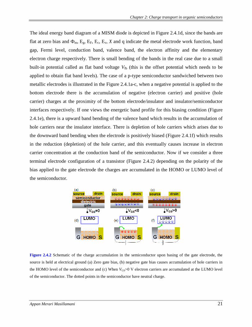
Chapter 2: Charge transport in organic semiconductors
Appan Merari Masillamani 21
The ideal energy band diagram of a MISM diode is depicted in Figure 2.4.1d, since the bands are
flat at zero bias and Фm, Eg, EF, Ec, Ev, X and q indicate the metal electrode work function, band
gap, Fermi level, conduction band, valence band, the electron affinity and the elementary
electron charge respectively. There is small bending of the bands in the real case due to a small
built-in potential called as flat band voltage Vfb (this is the offset potential which needs to be
applied to obtain flat band levels). The case of a p-type semiconductor sandwiched between two
metallic electrodes is illustrated in the Figure 2.4.1a-c, when a negative potential is applied to the
bottom electrode there is the accumulation of negative (electron carrier) and positive (hole
carrier) charges at the proximity of the bottom electrode/insulator and insulator/semiconductor
interfaces respectively. If one views the energetic band profile for this biasing condition (Figure
2.4.1e), there is a upward band bending of the valence band which results in the accumulation of
hole carriers near the insulator interface. There is depletion of hole carriers which arises due to
the downward band bending when the electrode is positively biased (Figure 2.4.1f) which results
in the reduction (depletion) of the hole carrier, and this eventually causes increase in electron
carrier concentration at the conduction band of the semiconductor. Now if we consider a three
terminal electrode configuration of a transistor (Figure 2.4.2) depending on the polarity of the
bias applied to the gate electrode the charges are accumulated in the HOMO or LUMO level of
the semiconductor.
Figure 2.4.2 Schematic of the charge accumulation in the semiconductor upon basing of the gate electrode, the
source is held at electrical ground (a) Zero gate bias, (b) negative gate bias causes accumulation of hole carriers in
the HOMO level of the semiconductor and (c) When VGS>0 V electron carriers are accumulated at the LUMO level
of the semiconductor. The dotted points in the semiconductor have neutral charge.

Chapter 2: Charge transport in organic semiconductors
Appan Merari Masillamani 22
According to the field applied from the gate electrode the charge density in the semiconductor
can be varied. The total amount of charges accumulated is proportional to the gate bias and the
capacitance of the dielectric (Ci).
When a bias is applied between the drain and the source (VDS), this potential difference gives rise
to a linear gradient across the channel. That is to say that at the source electrode where x=0 the
potential V(x) = 0 and when x = L (the channel length) V(x) = VDS. For a n-type channel when
VGS > VDS > 0, the current due to the flow of electrons as majority carriers in the channel
increases linearly, this regime is termed as the linear regime. When the value of the VDS is
increased to a value which is greater than the difference between VGS and threshold voltage (VT)
the drain current pinches-off and reaches saturation (appropriately named as saturation regime).
The working scheme of a transistor operating in both P and N channel modes is illustrated in
Figure 2.4.3.
Figure 2.4.3 Schematic of a transistor operation in P-Channel (b-d, top) and N-channel (b-d, bottom). For P-channel
when VGS < VDS holes start to flow towards the drain from the source and when the VDS exceeds the threshold
voltage (in magnitude) maximum number of charges are collected near the drain and a depletion region is formed in
its vicinity. For N-channel when VGS> VDS electrons start to flow towards the drain from the source and when the
VDS exceeds the threshold voltage maximum number of charges are collected near the drain and a depletion region is
formed in its vicinity.

Chapter 2: Charge transport in organic semiconductors
Appan Merari Masillamani 23
2.4.2 Transistor performance indicators
The performance of the transistor is estimated by some key parameters such as charge carrier
mobility, threshold voltage, Ion/Ioff ratio, turn on voltage and subthreshold slope. These
parameters can be extracted from the current vs. voltage (I-V) characteristics of the device.
Specifically two types of characteristics can be recorded namely,
(1) Output characteristics, and
(2) Transfer characteristics
The I-V characteristics for a field-effect transistor can be reasonably described according to the
gradual channel approximation. This condition is satisfied when the electric field perpendicular
through the channel is larger than that of the lateral field between the drain and the source (i.e.,
yExE yx // ) and this happens when the device channel length (L) is larger than the
dielectric thickness (di).
The output characteristics is the plot (Figure 2.4.4) which gives the variation in the drain current
(ID) with respect to the drain-source bias (VDS, this is referred as drain voltage frequently) at
fixed gate-source potential (VGS) values. The transfer characteristics (Figure 2.4.5) is the plot
which gives the variation in the ID with respect to the VGS, this is referred as drain voltage
frequently) at fixed values of VDS.
Figure 2.4.4 Typical output (ID vs. VDS) characteristics of a field-effect transistor. The curved dashed line intersects
the pinch-off points after which there is saturation of the ID.

Chapter 2: Charge transport in organic semiconductors
Appan Merari Masillamani 24
When the gate potential is greater than the threshold voltage the number of induced mobile
charges ( mobQ ) collected at the proximity of the source electrode is given by,
)( TGSimob VVCQ (2.11)
When taking into the account the position along the channel in the lateral direction (at a position
x) the induced charge density is expressed as,
))(( xVVVCQ TGSimob (2.12)
The magnitude of the drain current in the channel can be approximated as in absence of influence
to the charge carrier diffusion,
xmobeffD EQWI (2.13)
Where W is the channel width, and eff is the effective mobility taking into account of the
mobile carriers only.
The carrier mobility of electrons or holes is the average drift velocity per unit applied electric
field, in other words it provides an estimate of the maximum frequency of conductivity limit for
a material and it is related to the conductivity (σ) as,
m
qτ
m
nqnq where
2
(2.14)
Where q the elementary charge, m is the mass of the charge carrier, and is the frequency.
By substituting for the lateral electric field xE , with dV/dx results in,
dVxVVVCWdxI TGSieffD ))(( (2.15)
Using the gradual channel approximation the expression for the drain current can be obtained by
numerical integration from x= 0 to L (i.e., the lateral distance of separation between the source
and drain electrodes) and is expressed as shown in equation 2.16 in the linear regime,

Chapter 2: Charge transport in organic semiconductors
Appan Merari Masillamani 25
2
2
1)( DSDSTGSieffD VVVVC
L
WI (2.16)
This can be simplified since at the linear regime VDS << VGS,
DSTGSilinD VVVCL
WI )( (2.17)
Since the drain current is directly proportional to the linear carrier mobility, it can be estimated
from the transconductance (gmt) which is defined as the change in the drain current ( DI ) with
the gate source potential ( GSV ) at a constant VDS.24
DSiGS
Dlin
VWC
L
V
I.
(2.18)
Figure 2.4.5 Transfer characteristics of a field-effect transistor in (a) ID vs. VGS linear regime and (b) ID1/2
vs. VGS
saturation regime at a fixed VDS. The left and right axis illustrates the drain current in the linear and logarithmic
scales respectively. The drain current is expressed in absolute value, for a p-type (hole conducting) semiconductor
the sign of the drain current is negative and it’s the contrary for n-type semiconductor.
In the linear regime the x-axis inflection point from the plot of ID vs. VGS the threshold voltage of
the device can be extrapolated. After the threshold voltage (VT) there is saturation of the drain
current and the device goes into the on state, in other words it is the minimum potential required
to turn the transistor on. In the saturation regime it is gate voltage which is extracted from the x-
axis intercept from the ID1/2
vs. VGS plot (Figure 2.4.5b).
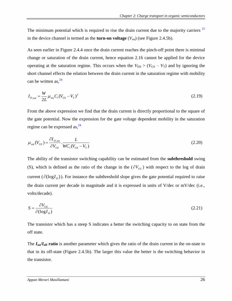
Chapter 2: Charge transport in organic semiconductors
Appan Merari Masillamani 26
The minimum potential which is required to rise the drain current due to the majority carriers 25
in the device channel is termed as the turn-on voltage (Von) (see Figure 2.4.5b).
As seen earlier in Figure 2.4.4 once the drain current reaches the pinch-off point there is minimal
change or saturation of the drain current, hence equation 2.16 cannot be applied for the device
operating at the saturation regime. This occurs when the VDS > (VGS – VT) and by ignoring the
short channel effects the relation between the drain current in the saturation regime with mobility
can be written as,24
2
,)(
2TGSitsasatD VVC
L
WI (2.19)
From the above expression we find that the drain current is directly proportional to the square of
the gate potential. Now the expression for the gate voltage dependent mobility in the saturation
regime can be expressed as,24
)(.)(
,
TGSiGS
satD
GSsatVVWC
L
V
IV
(2.20)
The ability of the transistor switching capability can be estimated from the subthreshold swing
(S), which is defined as the ratio of the change in the ( GSV ) with respect to the log of drain
current ( )(log DI ). For instance the subthreshold slope gives the gate potential required to raise
the drain current per decade in magnitude and it is expressed in units of V/dec or mV/dec (i.e.,
volts/decade).
)(log D
GS
I
VS
(2.21)
The transistor which has a steep S indicates a better the switching capacity to on state from the
off state.
The Ion/Ioff ratio is another parameter which gives the ratio of the drain current in the on-state to
that in its off-state (Figure 2.4.5b). The larger this value the better is the switching behavior in
the transistor.

Chapter 2: Charge transport in organic semiconductors
Appan Merari Masillamani 27
2.5 REFERENCES AND NOTES
1 Heeger, A. J. Nobel Lecture: Semiconducting and metallic polymers: The fourth generation of
polymeric materials. Rev. Mod. Phys. 73, 681-700 (2001).
2 Jaiswal, M. & Menon, R. Polymer electronic materials: a review of charge transport. Polym. Int.
55, 1371-1384 (2006).
3 Ostroverkhova, O. et al. Bandlike transport in pentacene and functionalized pentacene thin films
revealed by subpicosecond transient photoconductivity measurements. Phys. Rev. B 71, 035204,
(2005).
4 Coropceanu, V. et al. Charge transport in organic semiconductors. Chem. Rev. 107, 926-952,
(2007).
5 Sirringhaus, H. et al. Two-dimensional charge transport in self-organized, high-mobility
conjugated polymers. Nature 401, 685-688 (1999).
6 Le Comber, P. G. & Spear, W. E. Electronic Transport in Amorphous Silicon Films. Phys. Rev.
Lett. 25, 509-511 (1970).
7 Horowitz, G., Hajlaoui, M. E. & Hajlaoui, R. Temperature and gate voltage dependence of hole
mobility in polycrystalline oligothiophene thin film transistors. J. Appl. Phys. 87, 4456-4463
(2000).
8 Horowitz, G. & Hajlaoui, M. Grain size dependent mobility in polycrystalline organic field-effect
transistors. Synth. Met. 122, 185-189 (2001).
9 Chesterfield, R. J. et al. Variable temperature film and contact resistance measurements on
operating n-channel organic thin film transistors. J. Appl. Phys. 95, 6396-6405 (2004).
10 Majewski, L. A., Schroeder, R., Grell, M., Glarvey, P. A. & Turner, M. L. High capacitance
organic field-effect transistors with modified gate insulator surface. J. Appl. Phys. 96, 5781-5787
(2004).
11 Borsenberger, P. M. & Bassler, H. Concerning the role of dipolar disorder on charge transport in
molecularly doped polymers. J. Chem. Phys. 95, 5327-5331 (1991).
12 Bässler, H. Charge transport in disordered organic photoconductors a Monte Carlo simulation
study. phys. stat. sol. (b) 175, 15-56 (1993).
13 Miller, A. & Abrahams, E. Impurity Conduction at Low Concentrations. Phys. Rev. 120, 745-755
(1960).
14 Holstein, T. Studies of polaron motion: Part II. The “small” polaron. Ann. Phys. 8, 343-389
(1959).
15 Holstein, T. Studies of polaron motion: Part I. The molecular-crystal model. Ann. Phys. 8, 325-
342, (1959).
16 Marcus, R. A. Electron transfer reactions in chemistry. Theory and experiment. Rev. Mod. Phys.
65, 599-610 (1993).
17 Conwell, E. M. & Jeyadev, S. Free soliton transport and photoconductivity in trans-
polyacetylene. Synth. Met. 28, D439-D446, (1989).
18 Conwell, E. M., Choi, H. Y. & Jeyadev, S. Interchain polaron transport in trans-polyacetylene.
Synth. Met. 49, 359-365, (1992).
19 Alexandrov, A. S. & Yavidov, B. Y. Small adiabatic polaron with a long-range electron-phonon
interaction. Phys. Rev. B 69, 073101 (2004).
20 Bredas, J. L. & Street, G. B. Polarons, bipolarons, and solitons in conducting polymers. Acc.
Chem. Res. 18, 309-315, (1985).
21 Kreouzis, T. et al. Temperature and field dependence of hole mobility in poly(9,9-
dioctylfluorene). Phys. Rev. B 73, 235201 (2006).
22 Street, R., Salleo, A. & Chabinyc, M. Bipolaron mechanism for bias-stress effects in polymer
transistors. Phys. Rev. B 68, 085316 (2003).

Chapter 2: Charge transport in organic semiconductors
Appan Merari Masillamani 28
23 Lilienfeld, J. S. E. Method and apparatus for controlling electric currents. US patent 1745175
(1930).
24 Horowitz, G. Organic field-effect transistors. Adv. Mater. 10, 365-377 (1998).
25 Majority carriers are the carriers which are predominant in the semiconductor. For instance in a
n-type semiconductor the majority carriers are electrons, while in a p-type semicondcutor they
are holes. In ambipolar or bipolar semiconductor both electrons and holes can contribute to the
device current.

Chapter 3: Charge transport in molecular junctions
Appan Merari Masillamani 29
Nature may reach the same result in many ways.
-Nikola Tesla (1856-1943), Inventor/ Electrical engineering pioneer/ Wizard
3 3.1 CHARGE TRANSPORT IN MOLECULAR JUNCTIONS
In this chapter the fundamentals of the charge transport through molecular junctions is outlined.
The basic components of a molecular junction and its respective functions are elaborated. The
physics behind the charge transport phenomenon in particular tunneling process is explained.
The role of quantum tunneling and its use in molecular junctions particularly for electronics is
briefed.
3.1.1 Molecular junctions - building blocks
The field of molecular electronics as such was present in the mid of 21st century, but it was due
to a landmark proposition by Aviram and Ratner that an organic molecule could behave like a
rectifier1 brought in great interest from the research community. Their premise was molecule/s
with certain intrinsic functionality could be integrated into building more complex molecular
electronic circuits.2 A basic molecular junction is comprised of a single molecule or a set of
molecules attached to a metallic electrode. To understand the electron transport and the rates of
charge transfer vast number of molecular systems has been studied. A molecular junction based
on an azobenzene derivative is shown in Figure 3.1.1. The building units of molecular junction in
broad terms are comprised of molecules and electrodes. The electrodes can be either highly
conducting metal or carbon based structures such as nanotubes. The molecules bridging the
electrodes are in general much more resistive and in essence behave like an insulator, their
conductance increased if a high degree of conjugation along the molecular backbone is present.
Upon application of an electric field across the molecular junction charges start to flow from one
electrode to the other. Thus depending on the structure, type and length of π-conjugated bridge of
the molecule the electron transfer rates vary. For the purpose of electrical current rectification a
donor-bridge-acceptor (DBA) type of molecule was theoretically found be a suitable candidate.

Chapter 3: Charge transport in molecular junctions
Appan Merari Masillamani 30
Figure 3.1.1 Schematic of molecular junction (a) Molecule chemisorbed on Au electrode linking an acceptor unit
(b) Azobenzene molecule linking two conducting electrodes.
3.1.2 Metal-molecule-metal junctions
The link between the metal electrode and the molecule could range from strong covalently
bounded to weak van der Waals type of interaction. To understand how the charge transport
occurs in a molecular junction it is necessary to consider the molecular junction in terms of
individual components with respective energetic barriers among each of them.3,4
For instance,
metallic electrodes have uniform distribution of electronic states (DOS), while the molecules
have distinct conduction (LUMO) and valence (HOMO) levels separated by a band gap. The
offset between the respective electronic transport levels and the Fermi level of the metal contact
gives rise to a potential barrier.
Figure 3.1.2 shows the metal-molecule-metal junction at zero bias and with potential applied to
the electrodes. At zero bias the Fermi levels of the electrodes line up and there is a uniform
distribution of electronic charge across the metal contacts. Upon application of a positive bias to
the right electrode (RE) the Fermi level is lowered and there is a greater population of electronic
charge near the left electrode (LE). When the RE is negatively biased the Fermi level is raised
with respect to that of the LE resulting in a greater population of electronic charge near the RE.
The height of the tunneling barrier is denoted by ΦT,bh which changes corresponding to the
change in the electrical potential applied to the electrodes.

Chapter 3: Charge transport in molecular junctions
Appan Merari Masillamani 31
Figure 3.1.2 Illustration of the energy levels of a metal-molecule-metal junction at (a) Zero bias, (b) right electrode
negatively biased with respect to left electrode and (c) left electrode negatively biased with respect right electrode.
The current flowing in the molecular junctions is predominantly due to coherent tunneling and is
dependent on some factors such as,
(i) The composition of the molecular bridge and the electrodes
(ii) The strength of the metal-molecule or electrode-molecule interaction
(iii) The linking entity between the molecule and electrode
(iv) The Fermi energy of adjoining electrodes
(v) The electrostatic spatial charge distribution through the molecule

Chapter 3: Charge transport in molecular junctions
Appan Merari Masillamani 32
(vi) The orientation of the molecule
(vii) The roughness of the electrodes
(viii) The length and extent of conjugation along the molecular unit.
3.1.3 Quantum tunneling
When charge transport through a molecular layer of thickness < 5 nm is involved the
predominant mode by which the transport occurs is by a process what is termed by physicists as
quantum tunneling. In the view point of classical physics any electron with energy less than that
of the interfacial potential barrier at the metal/insulator interface always is reflected at the
interface. Depicted in Figure 3.1.3 is the quantum tunneling phenomenon of a particles in a wave
packet with mass m through a potential barrier V0 and distance l. The energetic state of the
particles are Gaussian distributed with momentum centered around the kinetic energy,
mkE 2/2
0
2 according to classical physics the particles do not possess enough energy to
surmount the barrier 0<x<l. However in terms of quantum mechanics which takes into account
the wave nature of the electrons provides the small possibility to traverse the forbidden region of
the barrier.
Figure 3.1.3 Quantum tunneling through one dimensional potential well with a barrier of height V0 and distance l.
The dotted purple line represents the tunneling decay which the wave packet undergoes upon encountering the
barrier.
The wavefunction associated with the electron decays exponentially with the depth of
penetration from its initial starting point at the metal/insulator interface. For macroscopic

Chapter 3: Charge transport in molecular junctions
Appan Merari Masillamani 33
thickness the decay is such that there is virtually zero probability to find an electron in the other
side of the interface. In the case that the barrier is very thin of the dimensions of less than 5 nm,
the wavefunction has a non-zero value at the opposite interface, thus there is finite probability
that the electron can pass from one electrode to the other by penetrating through the barrier. A
graphical illustration of the tunneling process in a metal-molecule-metal junction is shown in
Figure 3.1.4.
Figure 3.1.4 Quantum tunneling at a metal/insulator interface, illustrating the decay of the electron wavefunction
with distance l.
The electron wavefunction from metal electrode 1 rapidly decays as it passes through the
potential barrier induced by the presence of the molecule which behaves as an insulator. Note
that while there is an attenuation of the wavefunction the phase is maintained uniform
throughout. The rate of this coherent tunneling is given expressed in terms of the barrier width
and height in its simplest form according to Simmons model5,6
m
h
lm
lh
VqJ 2
4exp2
2
2 (1)
Where J is the current density (in A/cm2), q is the elementary charge, V is the applied potential,
h is Planck’s constant, m is the electron mass, Ф is the barrier height and l is the thickness of the
barrier. According to equation 1 the tunneling barrier is assumed to be rectangular.
For molecular junctions such as the case illustrated in Figure 3.1.2 the tunneling barrier height
ФT,bh is noted in units of Joules or electron volts.

Chapter 3: Charge transport in molecular junctions
Appan Merari Masillamani 34
To minimize the inherent complexity of the tunneling barrier profile the equation 1 is expressed
in its simplified approximation,
lAeJ (2)
Where A is a constant which refers to the current density in the case of a hypothetical barrier
with thickness l=0 and β (in Å-1
or nm-1
) is the rate of tunneling decay.
The charge tunneling through the molecule can be described by “through-bond” and “through-
space”.7,8
In through-bond tunneling the electron interaction with the molecular orbitals enhances
the rate of tunneling and is generally faster than through-space tunneling, thus through-bond
tunneling is frequently referred to as “superexchange”.8,9
However coherent tunneling process is
effective only for short distances of less than 3 nm since its decay rate is small ~0.5Å-1
.10-12
Figure 3.1.5 Illustration of coherent tunneling through a potential barrier induced by the molecule sandwiched
between two metal electrodes. The occupied electronic states in the electrodes are in dark gray/golden yellow
shades. The blue and red lines represent the LUMO and HOMO levels of the molecule. The Fermi level of the
electrodes lies between the molecular HOMO-LUMO gap.
For a distances greater than 3 nm the hopping is prevalent mode of transport.10,11

Chapter 3: Charge transport in molecular junctions
Appan Merari Masillamani 35
3.1.4 References and notes
1 Aviram, A. & Ratner, M. A. Molecular rectifiers. Chem. Phys. Lett. 29, 277-283 (1974).
2 Aviram, A. Molecules for memory, logic, and amplification. J. Am. Chem. Soc. 110, 5687-5692
(1988).
3 Nitzan, A. & Ratner, M. A. Electron transport in molecular wire junctions. Science 300, 1384-
1389 (2003).
4 McCreery, R. L. Molecular electronic junctions. Chem. Mater. 16, 4477-4496 (2004).
5 Simmons, J. G. Generalized formula for the electric tunnel effect between similar electrodes
separated by a thin insulating film. J. Appl. Phys. 34, 1793-1803 (1963).
6 Wang, W., Lee, T. & Reed, M. A. Mechanism of electron conduction in self-assembled
alkanethiol monolayer devices. Phys. Rev. B 68, 035416 (2003).
7 Slowinski, K., Chamberlain, R. V., Miller, C. J. & Majda, M. Through-bond and chain-to-chain
coupling. Two pathways in electron tunneling through liquid alkanethiol monolayers on mercury
electrodes. J. Am. Chem. Soc. 119, 11910-11919 (1997).
8 Segal, D., Nitzan, A., Davis, W. B., Wasielewski, M. R. & Ratner, M. A. Electron transfer rates
in bridged molecular systems 2. A steady-state analysis of coherent tunneling and thermal
transitions. J. Phys. Chem. B 104, 3817-3829 (2000).
9 Petrov, E. G., Shevchenko, Y. V., Teslenko, V. I. & May, V. Nonadiabatic donor--acceptor
electron transfer mediated by a molecular bridge: A unified theoretical description of the
superexchange and hopping mechanism. J. Chem. Phys. 115, 7107-7122 (2001).
10 Choi, S. H., Kim, B. S. & Frisbie, C. D. Electrical resistance of long conjugated molecular wires.
Science 320, 1482-1486 (2008).
11 Lu, Q. et al. From Tunneling to Hopping: A Comprehensive Investigation of Charge Transport
Mechanism in Molecular Junctions Based on Oligo (p-phenylene ethynylene) s. ACS nano 3,
3861-3868 (2009).
12 Kronemeijer, A. J. et al. Universal Scaling of the Charge Transport in Large‐Area Molecular
Junctions. small 7, 1593-1598 (2011).

Chapter 4: Methods and Procedures
Appan Merari Masillamani 37
Design is not just what it looks like and feels like. Design is how it works.
-Steve Jobs (1955-2011), Visionary entrepreneur
4 Methods and
Procedures
4.1 OFET PREPARATION
OFETs with two different device geometries were fabricated during the course of this thesis
namely,
(i) Bottom-gate bottom-contact and
(ii) Top-gate bottom-contact.
The deposition of the active semiconducting layer was carried out by means of either spin
casting or drop casting from respective solutions.
4.1.1 F8BT based OTFTs
Poly[(9,9-di-n-octylfluorenyl]-2,7-diyl)-alt-(benzo[2,1,3]thiadiazol-4,8-diyl)] (Aldrich)
abbreviated as F8BT was the organic semiconductor in all the devices. Poly(methyl
methacrylate) (PMMA, Mw = 4, 50, 500 kgmol-1
, Aldrich) and Polystyrene of three different
molecular weights (PS, Mw = 4, 48.1, 500 kgmol-1
, Aldrich) served as the polymer gate dielectric.
All materials were used as received without further purification. The organic thin film transistors
were fabricated on n++
- Si/SiO2 wafer (IPMS Fraunhofer, Germany), which served as support
substrates. The substrates were cleaned by thoroughly rinsing in acetone followed by sonication
at room temperature with acetone (≥ 99.5% purity) and 2-propanol for 15 minutes respectively
and dried under a steady stream of nitrogen. Interdigitated gold source-drain electrodes (30 nm)
were then evaporated with a shadow mask using Plassys MEB 300 thermal evaporator at 0.04-
0.06 nms-1
. The evaporation of the electrodes prior to the deposition of semiconductor ensured
no gold atoms penetrate into the semiconductor layer thereby hindering carrier injection.
Undecanethiol (Aldrich) self-assembled monolayer was coated on the Au electrodes by
incubation of the substrates in 1 mM thiol solution (in ethanol) overnight. After removal of the
substrates from the thiol solution they were rinsed with copious amount of the ethanol solvent to

Chapter 4: Methods and Procedures
Appan Merari Masillamani 38
remove any physisobred molecules on the electrodes. The next step was the surface passivation
of the SiO2 by hexamethyldisilazane (HMDS) vapor treatment of the substrates overnight prior
to deposition of the semiconducting layer. F8BT in chloroform (6 mg mL-1
) was spin coated at
1800 rpm and subsequently annealed at 80ºC for 10 minutes. After allowing the substrates to
cool down, PMMA and PS of appropriate concentration in anhydrous n-butyl acetate were spin
coated at different speeds which gave a thickness of (~ 620 nm), the substrates were then
annealed immediately at 80ºC for 1 hour to allow evaporation of any solvent which might be
trapped in the film. After annealing the substrates were allowed to cool for 1 hour before
evaporation of the top gate gold electrode (30 nm) with a shadow mask, manually aligned under
an optical microscope this completed the fabrication of the device with top-gate bottom-contact
device geometry. The complete fabrication cycle of the OTFT is depicted in Figure 4.1.1. The
spin coating and annealing of the organic semiconductor and polymer dielectric was carried out
entirely under inert atmosphere in a nitrogen filled glove box.
Figure 4.1.1 Fabrication cycle of top-gate bottom-contact F8BT based OTFT comprising of the following steps, (i)
evaporation of gold source-drain electrodes on bare Si/SiO2 substrate, (ii) treatment of Au electrodes with
undecanethiol, (iii) Passivation of the SiO2 surface by with HMDS vapor overnight, (iv) Spin coating F8BT to form
the active layer, (v) Spin casting of the dielectrics PMMA or PS from n-butyl acetate, and (vi) evaporation of 30 nm
Au to form the top-gate electrode.

Chapter 4: Methods and Procedures
Appan Merari Masillamani 39
4.1.2 P3HT based OTFTs
1.51.5 cm2
Si/SiO2 substrates (IPMS Fraunhofer) comprising of thermally grown SiO2 layer on
a n++
Si, which served as the gate, and pre-patterned Au electrodes deposited on the SiO2 layer,
which served as source-drain electrodes, were used to fabricate the thin-film transistor. The
substrates were cleaned by rinsing with acetone to remove the photoresist film followed by
sonication in an ultrasonic bath (Fisher) with acetone and isopropanol for 15 minutes each. The
channel length (L) and width (W) for the TFTs which were characterized amounted to 10 and
10000 µm, respectively. To complete the OTFT device a poly(3-hexylthiophene) (P3HT)
solution (120 µl of 2 mg ml-1
in toluene) was spin-coated on the substrates. After spin-coating of
P3HT the solvent was allowed to evaporate for ~ 48 h prior to electrical characterization.
4.1.3 QQT(CN)4 based OFETs
For p and n-type operation: Devices were fabricated by spin casting 50 µL QQT(CN)4 from
CHCl3 onto substrates with pre-patterned electrodes (IPMS Fraunhofer, Germany).
n-type operation: Devices were fabricated by spin casting QQT(CN)4 onto pre-patterned
substrates followed by an annealing step at 180 °C for 10 s in ambient conditions.
4.1.4 P3HT, diarylethene blend OFETs
P3HT+DAE_open blend OFET: DAE of 20% by weight was blended with P3HT at a
concentration of 1 mg mL-1
in chloroform. The blend solution was then spin coated onto a
Si/SiO2 substrate comprising of pre-patterned interdigitated electrodes (IPMS Fraunhofer,
Germany). Heavily n doped Si layer served as the gate electrode, thermally grown SiO2 layer was
the gate dielectric (Ci =15 nF cm-2
). In the case of the P3HT with DAE_open form, the solution
was plainly spin casted and allowed to cure inside a N2 filled Jacomex glovebox (O2 < 5 ppm,
H2O < 0.6 ppm) for 15 minutes.
P3HT+DAE_closed blend OFET: The starting substrate was similar to the OFETs based on
DAE_open and P3HT but after spin coating of the blend solution, the substrate was irradiated
with UV light at a λ of 366 nm for 10 minutes to convert the DAE_open molecules embedded in
the bulk of the blend film to its ring closed state. For this end the substrate was held in the chuck
of the spin coater and the UV light was irradiated on the large face ensuring maximum amount of
exposure to the light on the semiconducting thin film.

Chapter 4: Methods and Procedures
Appan Merari Masillamani 40
Encapsulation of OFETs: To improve the stability of the OFET in ambient conditions the OFETs
were encapsulated with a film of PMMA. The concentration of 50 mg ml-1
PMMA in methyl
ethyl ketone was spin casted directly on top of the semiconducting film for devices with DAE in
both states.
4.1.5 P3HT, PTTP blend OFETs
The base substrates for transistors with a blend of poly(3-hexylthiophene) (P3HT) and PTTP as
the active layer in the film was pre-patterned Fraunhofer ones. The amount of the ratio of the
PTTP by weight in blend with P3HT varied from 0, 5, 25, 75, 95 and 100 %. The concentration
of the solution used for all the blend cases were 5 mg mL-1
in para-xylene. To fabricate the
transistors 100 µL of blend solution was drop casted onto the substrates and allowed to cure in an
inert N2 filled atmosphere of glovebox.
4.2 OFET CHARACTERIZATION TECHNIQUES
For performing the charge transport measurements in the OFETs characterization was performed
in a standard probe station setup inside a glovebox for air-sensitive devices while
characterization was performed in ambient conditions for air stable devices. For probing the
temperature dependent behavior in OFETs a setup interfaced with a static cryostat was
employed.
4.2.1 Electrical characterization inside glovebox
This characterization was performed by means of a dual channel source meter (Keithley 2636A
SMU) in the dark. Triaxial cables were employed to minimize signal losses. The OFET under
test was placed in a sample stage of Cascade Mikrotek probe station and probed by means of
süss probes. For all the cases when the devices were air-sensitive the complete electrical
characterization were performed inside a N2 filled glovebox (Jacomex) with O2 levels < 10 ppm.
The levels of O2 and H2O in the glovebox were periodically monitored.
4.2.2 Electrical characterization in cryostat
A static cryostat OptistatDN (Oxford instruments, UK) was employed to house the OFET. The
electrical contact with the OFET were realized by means of a custom built sample pad (Figure
4.2.1c) which could be mounted or dismounted from the protruding electrical connector pins.
The connections to the OFET electrodes were then established between first by affixing the gate

Chapter 4: Methods and Procedures
Appan Merari Masillamani 41
electrode and a copper pad by means of conductive silver adhesive (Figure 4.2.1d) and the source-
drain electrode pads were connected to their respective terminals with copper wires (0.1mm
diameter). Teflon tapes were wrapped around the soldered joints of the cable with the connector
pins, to provide shielding over the contacts. The cryostat was interfaced with an external dual
channel electrometer Keithley 2636A (Keithley Instruments Inc, USA) with coaxial cables from
the SMB sockets for each of the individual electrodes (Figure 4.2.1).
Figure 4.2.1 Photographs illustrating the connection sequence of an OFET with the cryostat sample rod (a and b)
electrical connector pins, (c) OFET holder pad plugged into the connector pins and (d) OFET affixed to the sample
holder pad with electrical connections established at source, drain and gate electrodes. Green bar represents the scale
of 1 cm.
Figure 4.2.2 shows the entire setup schematic of the cryostat along with the external temperature
control unit and the electrometer. Temperature control was maintained and monitored by an
intelligent temperature controller (ITC) unit attached to a heating sensor of the cryostat. Once the
OFET was attached to the sample rod and placed in the cryo sample space, it was pumped to
high vacuum. The sample space was cooled by thermal conduction due to heat exchanged by the
flow of nitrogen gas in contact with liquid nitrogen reservoir. Prior to loading the sample rod the
outer vacuum chamber was pumped to high vacuum to ensure good thermal isolation. The
temperature was regulated by the manual flow of nitrogen gas and the heating of the sensor
controlled by the electrical power dispensed from the ITC.
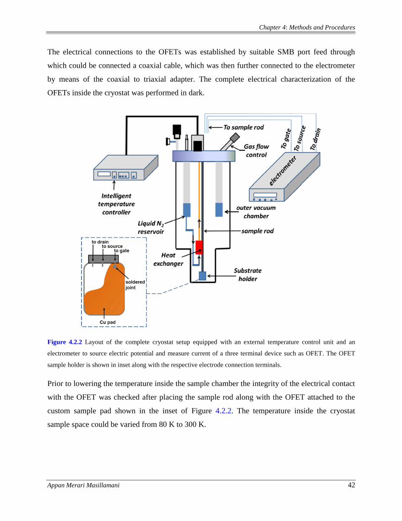
Chapter 4: Methods and Procedures
Appan Merari Masillamani 42
The electrical connections to the OFETs was established by suitable SMB port feed through
which could be connected a coaxial cable, which was then further connected to the electrometer
by means of the coaxial to triaxial adapter. The complete electrical characterization of the
OFETs inside the cryostat was performed in dark.
Figure 4.2.2 Layout of the complete cryostat setup equipped with an external temperature control unit and an
electrometer to source electric potential and measure current of a three terminal device such as OFET. The OFET
sample holder is shown in inset along with the respective electrode connection terminals.
Prior to lowering the temperature inside the sample chamber the integrity of the electrical contact
with the OFET was checked after placing the sample rod along with the OFET attached to the
custom sample pad shown in the inset of Figure 4.2.2. The temperature inside the cryostat
sample space could be varied from 80 K to 300 K.

Chapter 4: Methods and Procedures
Appan Merari Masillamani 43
4.2.3 Work function of electrodes
The work functions of the metal and gold-SAM electrodes were measured by means of
macroscopic Kelvin probe (Kelvin Probe Technology Ltd, UK) or ambient ultraviolet
photoelectron spectroscopy (UPS) (Riken AC2 spectrophotometer, Japan).
The contact potential difference method, using a commercial Au reference tip was employed to
record the work function of the Au and Au-SAM surface.
Using the UPS (Figure 4.2.3) the work function of Au which was estimated by the minimum
threshold energy required for commencement of photoelectrons from the ground state.
4.2.4 Ionization energy of semiconductor film
The ionization energy levels of our semiconductor films were recorded by means of ambient
UPS from Riken Keiki Co Ltd model AC-2. The ionization energy (IE) gives the lowest energy
required to create a hole in the highest occupied molecular orbital upon the photoemission of an
electron.
Figure 4.2.3 Schematic layout of the UPS with illustration of the basic working principle of the setup. The incident
UV beam arrives at the surface of the sample under test through an optical fiber at an angle of 30°.
For F8BT film, firstly ~120 µL of 6 mg mL-1
F8BT solution in CHCl3 was drop casted onto a
custom solution holder inside N2 filled glovebox and the solvent was allowed to dry.

Chapter 4: Methods and Procedures
Appan Merari Masillamani 44
For QQT(CN)4 films, 50 µL of varying concentration of 1, 2, 3, 5, 8 mg mL-1
QQT(CN)4
solution in CHCl3 was casted from solution onto cleaned ITO substrates in ambient conditions
after which the IE levels were recorded.
For P3HT film, the IE was recorded after drop casting and curing of 2 mg mL-1
P3HT in toluene
onto a metallic solution holder inside the glovebox.
4.2.5 Morphological characterization
The morphology of the semiconductor films, dielectric films and the Au electrodes of the OFETs
was mapped by atomic force microscopy (AFM) from Digital Instruments Dimension 3100
(Bruker Instruments Inc, USA) operating in the intermittent-mode.
4.2.6 Microstructural characterization of P3HT:PTTP blend films
GIWAXS measurements were performed using a custom setup consisting of rotating anode X-
ray source (Rigaku Micromax, operated at 42kV and 20mA), Osmic confocal MaxFlux optics
and a three pin-hole collimation system (JJ X-ray). Samples on the top of approx. 1.51.5 cm
silicon platelets were irradiated at the incident angle (i) of 0,20°. Diffraction patterns were
recorded for 3h on a MAR345 image plate detector. Finally, the data was processed and imaged
using Datasqueeze 2.2.5 program. For one-dimensional XRD, a θ-θ Siemens D500 Kristalloflex
with a graphite-monochromatized CuKα X-ray beam was used.
4.2.7 Surface wettability tests
The aqueous contact angle at the SAM-ambient interface was measured by means of a Krüss
DSA 100 goniometer (Krüss GmbH, Germany). The contact angle and the derived work of
adhesion provided qualitative information on the surface wettability of electrodes incorporated in
OTFTs.
The contact angle characterization was also performed on PMMA, PS and F8BT films to
elucidate the surface wettability and thereby the corresponding surface free energy.
4.2.8 UV/Vis spectroscopy on films
Absorbance spectrum of the spin cast blend film of P3HT and 20% weight DAE_open (2 mg
mL-1
) on quartz slides were acquired by means of a Jasco V-670 spectrophotometer (Jasco
analytical instruments Inc, USA).

Chapter 4: Methods and Procedures
Appan Merari Masillamani 45
The absorption spectrum of spin coated QQT(CN)4 films pre and post annealing was recorded
with by UV/Vis spectrophotometer. To this end 50 µL of QQT(CN)4 in CHCl3 was spin coated
onto quartz substrates after which the absorption spectrum on this film was collected.
4.3 SAM PREPARATION
Depending on the air stability of the molecules used to form the self-assembled monolayer
(SAM), it was either formed inside an inert glovebox or in ambient laboratory conditions.
The preparation of the SAM on gold substrate follows the steps as depicted in Figure 4.3.1.
Firstly the Au substrate is cleaned by gently blowing with a N2 followed by UV/Ozone
treatment. Once the cleaning procedure of the Au surface is done the substrate is immediately
immersed in the respective thiol solution for a predetermined amount of time to allow the
formation of the SAM on the surface of the gold. After the removal of the Au substrate from the
thiol solution the substrate is rinsed with the solvent in which the thiol molecules are dissolved in
for at least 20 times by splashing the solvent from the pipette and always holding the substrate at
the bottom edge with a pair of tweezers as illustrated in Figure 4.3.1. Once the solvent drips off
the surface of the Au substrate it is gently blow dried with a stream of the N2 to remove any
residual solvent which might be entrapped between the molecules.
Figure 4.3.1 Illustration of the preparation steps of SAM on a gold substrate. The purple symbols represent the
molecules which chemisorb onto the gold surface.
For biphenylthiol family of SAMs: Firstly the 1mM biphenylthiol solutions in CHCl3 were
prepared and stored in an inert N2 filled atmosphere of a glove box (Jacomex). Next for X-ray
spectroscopy and charge transport measurements with GaInE setup the SAMs were prepared on

Chapter 4: Methods and Procedures
Appan Merari Masillamani 46
commercial gold (111) evaporated on mica substrates (Georg Albert PVD, Germany) with Au
thickness of 300 nm. The substrates were immersed and incubated in the corresponding 1mM
biphenyl thiol solution under N2 atmosphere for 24 h to obtain the desired monolayers. For work
function and contact angle experiments, 50 nm Au were evaporated on glass slides with an
adhesion Cr layer of 10 nm at a base pressure of ~10-6
mbar in a Plassys MEB 300 thermal
evaporator and then immediately immersed in the respective biphenylthiol solution for 24 h
under inert conditions inside the glovebox. For all the experiments, once removed from the thiol
solution the substrates were rinsed with generous amount of CHCl3 in ambient conditions. All
the substrates were treated with UV/Ozone prior to immersion in the respective thiol solutions
for SAM formation.
For fluorinated azobenzene SAMs with mono and biphenyl substitutions: Solution
concentration of fluorinated azobenzene (Fazo) of 10 μM in chloroform was prepared and stored
in a cool dark environment (inside refrigerator).
To form Fazo SAM in trans form in the Fazo solution for a period of 24 h in a beaker under
standard laboratory conditions (SLC).
To form Fazo SAM in cis conformational form, firstly the Fazo solution was irradiated with UV
light at the wavelength of 366 nm (8 W intensity) for duration of 120 s, during which due to
process of photo-isomerization the Fazo molecules changes the confirmation from trans → cis
confirmation (as confirmed by the change in intensity of absorption of the UV/vis spectrum).
Then the Au(111) substrate on mica was immediately immersed in the Fazo cis solution and
stored inside a refrigerator at 4 °C for a period of 24 h to allow the formation of the Fazo SAM in
its cis isomeric state.
After 24 h once the trans and cis SAM were formed, were rinsed with the solvent in which the
Fazo molecules were dissolved in. Since CHCl3 was used as the solvent for the Fazo, the Au-
Fazo SAM substrates were rinsed with abundant quantity of the same solvent.
4.4 SAM CHARACTERIZATION TECHNIQUES
The electrical characterization of the SAMs were performed by means of a custom built two
terminal setup and the structural characterization of the SAMs were performed by means of high

Chapter 4: Methods and Procedures
Appan Merari Masillamani 47
resolution X-ray photoelectron spectroscopy (HRXPS) and angle-resolved near-edge X-ray
absorption fine structure spectroscopy (NEXAFS).
4.4.1 Electrical characterization of SAMs
To estimation of the rate of charge transport through the SAMs on Au electrodes was
experimentally performed by means of a two terminal setup which comprised of a eutectic liquid
metallic gallium-indium alloy (GaInE) which was employed as a top-probe electrode. An airtight
digital syringe (Hamilton N cemented needle pst3, 25µl, with a 90° bevel nozzle edge fitted to a
digital dispenser 22S gauge) held an adequate reservoir of GaInE which could be manipulated to
dispense the alloy in a controlled manner, which was then molded to a conical shaped tip (see
Figure 4.4.1). The junction comprising the SAM sandwiched between Au and GaInE
could be
realized very accurately by means of a servo controlled xyz stage (MT3-Z8, THORLABS) via
careful approach of the GaInE tip. This was accomplished by raising the stage supporting the Au-
SAM substrate by means of a DC servo motor controller (T-Cube, THORLABS) interfaced to
the supporting platform with an actuator (Z8 actuator, THORLABS) to gently establish contact
with the apex of the hanging GaInE tip (monitored in real-time using a CCD camera).
To ensure a greater control during approach in the z-axis direction (vertical) and higher
versatility of movement in the x-y axes direction (lateral) we kept the position of the syringe
holding the GaInE tip fixed, thereby only moving the stage supporting the sample. The complete
setup of the setup is shown in Figure 4.4.1.
The entire setup was placed on a bulky concrete stage free from minute vibrations and housed in
a custom made Faraday cage to provide electrostatic shielding and triaxial cables were used to
minimize signal losses. The necessary potentials across the junctions were provided by an
external supply unit Keithley 2635 source measure unit interfaced through a 2600-ALG-2
(Keithley instruments Inc) cable to minimize signal losses.
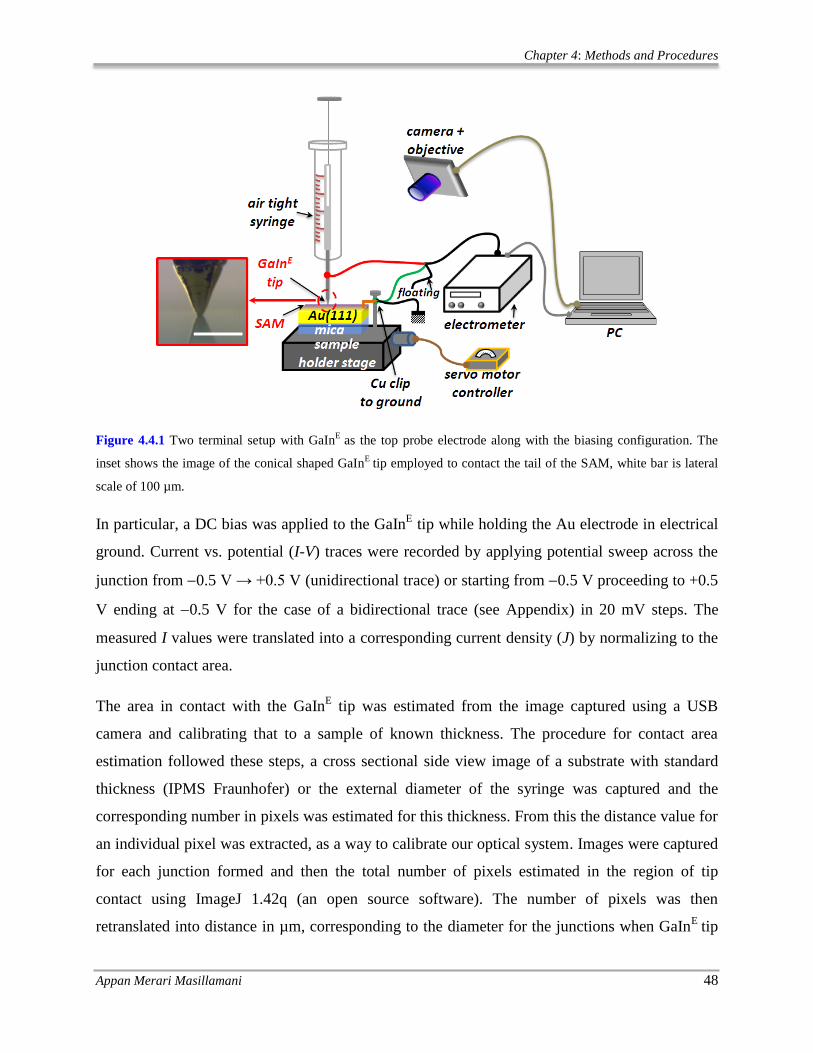
Chapter 4: Methods and Procedures
Appan Merari Masillamani 48
Figure 4.4.1 Two terminal setup with GaInE
as the top probe electrode along with the biasing configuration. The
inset shows the image of the conical shaped GaInE
tip employed to contact the tail of the SAM, white bar is lateral
scale of 100 µm.
In particular, a DC bias was applied to the GaInE tip while holding the Au electrode in electrical
ground. Current vs. potential (I-V) traces were recorded by applying potential sweep across the
junction from 0.5 V → +0.5 V (unidirectional trace) or starting from 0.5 V proceeding to +0.5
V ending at 0.5 V for the case of a bidirectional trace (see Appendix) in 20 mV steps. The
measured I values were translated into a corresponding current density (J) by normalizing to the
junction contact area.
The area in contact with the GaInE tip was estimated from the image captured using a USB
camera and calibrating that to a sample of known thickness. The procedure for contact area
estimation followed these steps, a cross sectional side view image of a substrate with standard
thickness (IPMS Fraunhofer) or the external diameter of the syringe was captured and the
corresponding number in pixels was estimated for this thickness. From this the distance value for
an individual pixel was extracted, as a way to calibrate our optical system. Images were captured
for each junction formed and then the total number of pixels estimated in the region of tip
contact using ImageJ 1.42q (an open source software). The number of pixels was then
retranslated into distance in µm, corresponding to the diameter for the junctions when GaInE
tip
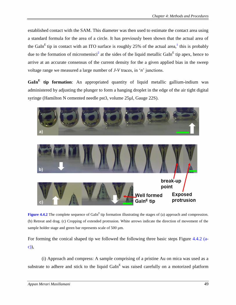
Chapter 4: Methods and Procedures
Appan Merari Masillamani 49
established contact with the SAM. This diameter was then used to estimate the contact area using
a standard formula for the area of a circle. It has previously been shown that the actual area of
the GaInE
tip in contact with an ITO surface is roughly 25% of the actual area,1 this is probably
due to the formation of micromenisci2 at the sides of the liquid metallic GaIn
E tip apex, hence to
arrive at an accurate consensus of the current density for the a given applied bias in the sweep
voltage range we measured a large number of J-V traces, in ‘n’ junctions.
GaInE tip formation: An appropriated quantity of liquid metallic gallium-indium was
administered by adjusting the plunger to form a hanging droplet in the edge of the air tight digital
syringe (Hamilton N cemented needle pst3, volume 25µl, Gauge 22S).
Figure 4.4.2 The complete sequence of GaInE
tip formation illustrating the stages of (a) approach and compression.
(b) Retreat and drag. (c) Cropping of extended protrusion. White arrows indicate the direction of movement of the
sample holder stage and green bar represents scale of 500 µm.
For forming the conical shaped tip we followed the following three basic steps Figure 4.4.2 (a-
c)),
(i) Approach and compress: A sample comprising of a pristine Au on mica was used as a
substrate to adhere and stick to the liquid GaInE
was raised carefully on a motorized platform

Chapter 4: Methods and Procedures
Appan Merari Masillamani 50
until it reached the hanging GaInE
droplet. Once the Au surface established contact with the
GaInE
the sample platform was further raised until it compressed the GaInE
droplet roughly until
the hemisphere shape was reached (Figure 4.4.2a).
(ii) Retreat and drag: After the stage of attainment hemisphere GaInE shape the
motorized support stage was retreated during which the quantity of GaInE which got adhered to
the surface got dragged until it reached the break-up point. Upon further downward movement of
the stage results in a distinct top and bottom conically shaped tip with a small protrusion.
(iii) Crop and trim: The protrusion extending from the conical tip then needed to be
removed, this was done by approach until adequate contact just to extent until the protrusion
distance is compressed and then the stage is pull down which leaves a freshly formed conical
shaped tip.
The entire tip formation sequence takes ~30 – 40 s. It necessitates that the shape of the conical
tip are well-defined which makes the estimate of area for the junctions formed more precise.
4.4.2 Structural characterization of SAMs
For the biphenylthiol family of SAMs HRXPS and NEXAFS characterization methods were
employed to shed light into quality of the SAMs on Au(111) according to the following
conditions,
X-ray spectroscopy measurements: The structural characterization of the SAMs was
performed by means of synchrotron-based HRXPS and NEXAFS spectroscopy. The HRXPS and
NEXAFS spectroscopy experiments were performed at the bending magnet HE-SGM beamline
at the synchrotron storage ring BESSY II in Berlin, Germany. The measurements were carried
out under room temperature and ultra-high vacuum (UHV) conditions with a base pressure of at
least 1.5 x 10⁻⁹
mbar or higher. High precaution was exercised by selecting the time for spectral
acquisition such that no noticeable sample damage by the primary X-rays was observed during
the measurements.3-5
The spectra were recorded in normal emission geometry. C 1s, S 2p, and Au
4f HRXPS spectra were acquired at photon energies (PEs) of 350 and 580 eV. The O 1s spectral
range was monitored and the binding energy (BE) scale was referenced to the position of the Au
4f7/2 emission line of Au substrate comprising a SAM of dodecanethiol at 83.95 eV energy value

Chapter 4: Methods and Procedures
Appan Merari Masillamani 51
which is given by the latest ISO standard.6 The energy resolution was ~0.3 eV at a PE of 350 eV.
The resulting HRXPS spectra was fitted by symmetric Voigt functions of either a Shirley-type or
linear background, the fits were performed self-consistently (i.e., the same peak parameters were
used in identical regions of the spectrum) which resulted in the spectrum accuracy for the BE at
FWHM values in the range of 0.05 eV. In the case of the S 2p3/2,1/2 doublets we used a pair of
peaks with the same FWHM, a branching ratio of 2 (2p3/2/2p1/2), and a spin-orbit splitting
verified by the fit of ~1.18 eV.7
The NEXAFS spectra were acquired at C K-edge in partial electron yield mode with a retarding
voltage of 150 V and linearly polarized light with a polarization factor of ~91%. To gather
details of the orientational order of the SAMs the angle of the incident light was varied from 90º
to 20º in steps of 10º-20º which corresponds to progression of the E vector from the surface
normal to the plane close to the sample surface.8 The energy resolution of the spectra was ~0.3
eV. The raw NEXAFS spectrum of each sample was normalized by dividing by the incident
photon flux for a clean gold reference sample9 and the energy scale was gauged to the most
pronounced π* resonance of highly oriented pyrolytic graphite at 285.38 eV.10
4.5 REFERENCES
1 Nijhuis, C. A., Reus, W. F. & Whitesides, G. M. Molecular Rectification in Metal−SAM−Metal
Oxide−Metal Junctions. J Am Chem Soc 131, 17814-17827, (2009).
2 Timsit, R. S. The True Area of Contact at a Liquid Metal-Solid Interface. Appl Phys Lett 40, 379-
381 (1982).
3 Jäger, B. et al. X-ray and Low Energy Electron Induced Damage in Alkanethiolate Monolayers
on Au-substrates. Z. Phys. Chem. 202, 263-272, (1997).
4 Wirde, M., Gelius, U., Dunbar, T. & Allara, D. L. Modification of self-assembled monolayers of
alkanethiols on gold by ionizing radiation. Nucl. Instrum. Methods Phys. Res., Sect. B 131, 245-
251, (1997).
5 Zharnikov, M. & Grunze, M. Modification of thiol-derived self-assembling monolayers by
electron and x-ray irradiation: Scientific and lithographic aspects. J Vac Sci Technol B 20, 1793-
1807 (2002).
6 X-ray photoeletron spectrometers-Calibration of the energy scales. ISO 15472 Surface chemical
analysis (2001).
7 Azzam, W., Wehner, B. I., Fischer, R. A., Terfort, A. & Wöll, C. Bonding and orientation in self-
assembled monolayers of oligophenyldithiols on Au substrates. Langmuir 18, 7766-7769 (2002).
8 Stöhr, J. NEXAFS spectroscopy. (Springer-Verlag, 1992).
9 Frey, S. et al. Structure of Thioaromatic Self-Assembled Monolayers on Gold and Silver.
Langmuir 17, 2408-2415, (2001).
10 Batson, P. E. Carbon 1s near-edge-absorption fine structure in graphite. Phys Rev B 48, 2608-
2610 (1993).


Chapter 5: Organic Field-Effect Transistors
Appan Merari Masillamani 53
No problem can withstand the assault of sustained thinking.
-François-Marie Arouet Voltaire (1694-1778), Philosopher
5 Organic Field-
Effect Transistors
5.1 DIELECTRIC MOLECULAR WEIGHT INFLUENCE IN AMBIPOLAR F8BT OFETS
Gate dielectrics in organic field-effect transistors play a vital role in governing the overall
performance of the device since the charge transport channel is formed in the active layer of the
device at the interface with the dielectric. To effectively modulate the transistor function
dielectric surface modification offers a viable and highly feasible strategy. In this part we discuss
the influence of varying the dielectric molecular weight on the device stability and reliability.
The change in the molecular weights induces subtle changes to the surface free energy and
polarity, the interplay between these influences charge carrier mobility, trapping and hysteresis.
The mechanism of rates of channel current decay upon continuous operation for both hole and
electron carriers are discussed according the bipolaron trapping model.
5.1.1 Scope
Research in the development of Organic thin-film transistors (OTFTs) has attracted considerable
interest in the past two decades owing to distinctive advantages such as reduced fabrication
complexity, significantly lower manufacturing costs and thus paving a way towards potential
applications in flexible large area electronics,1,2
radio-frequency identification (RFID) tags3 and
e-paper.4 Traditionally SiO2 had been used as the dielectric of choice in the OTFTs since it has
high dielectric breakdown strength and is less prone to gate leakage currents i.e., current flowing
from the gate electrode upon polarization of the dielectric layer under the influence of an
electrical field between the gate and source electrodes. However for the realization of transistors
on light-weight flexible substrates, polymeric dielectrics are a better alternative which can nearly
match the SiO2 in terms of leakage losses.5 Polymeric dielectrics offer further benefits of easy
deposition, solution processability, variable surface adhesion/wetting properties, higher range of
dielectric constants and surface free energies. The surface roughness of the dielectric has been
shown to affect the overall device performance,6 the surface chemistry has been shown to

Chapter 5: Organic Field-Effect Transistors
Appan Merari Masillamani 54
influence the densities of traps in OTFTs,7 the polymer tacticity has been shown to influence the
gate leakage,8 the surface glass transition temperature which affects the polymer chain motion
9
and surface free energy of the polymeric dielectrics has been shown to influence charge carrier
mobilities in vapor deposited organic semiconductors.7,10-12
Since the conductance, mobility, and switching capability of the transistor is governed by the
carrier channel formed in the semiconductor layer at the interface with the dielectric,13-15
the
surface properties of the dielectric play a vital role in the outcome of the device function.14,16,17
Until now there is no systematic study in the literature on the stability and reliability of top gate
TFTs based on solution deposited semiconductor-dielectric films to the best of our knowledge.
To understand the influence of transistor performance by varying molecular weights of the
polymeric dielectric layer in OTFT, in this article we consider two different polymeric dielectrics
poly(methyl methacrylate) (PMMA) and polystyrene (PS) of low, medium and higher molecular
weights (Mw) casted from solution on an organic semiconductor in a top-gate bottom-contact
(TGBC) device layout (Figure 5.1.1). PMMA and PS were chosen as dielectrics since the
chemical structural variation between the aromatic styrene and aliphatic methyl methacrylate
units induces different degree of surface polarity, and more particularly the dielectric constants
(k) of 3.6 and 2.6 respectively for these two dielectrics was not too different, hence we could
characterize and compare quantitatively the parameters affecting the transistor performance,
stability and reliability.
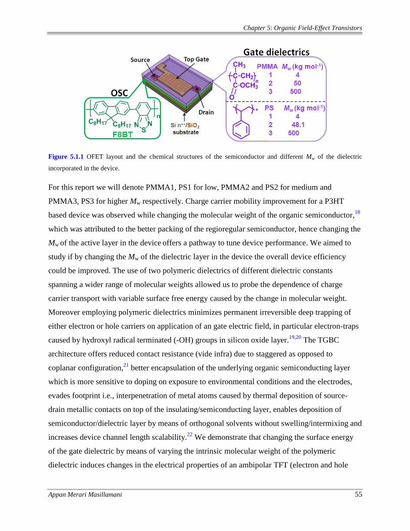
Chapter 5: Organic Field-Effect Transistors
Appan Merari Masillamani 55
Figure 5.1.1 OFET layout and the chemical structures of the semiconductor and different Mw of the dielectric
incorporated in the device.
For this report we will denote PMMA1, PS1 for low, PMMA2 and PS2 for medium and
PMMA3, PS3 for higher Mw respectively. Charge carrier mobility improvement for a P3HT
based device was observed while changing the molecular weight of the organic semiconductor,18
which was attributed to the better packing of the regioregular semiconductor, hence changing the
Mw of the active layer in the device offers a pathway to tune device performance. We aimed to
study if by changing the Mw of the dielectric layer in the device the overall device efficiency
could be improved. The use of two polymeric dielectrics of different dielectric constants
spanning a wider range of molecular weights allowed us to probe the dependence of charge
carrier transport with variable surface free energy caused by the change in molecular weight.
Moreover employing polymeric dielectrics minimizes permanent irreversible deep trapping of
either electron or hole carriers on application of an gate electric field, in particular electron-traps
caused by hydroxyl radical terminated (-OH) groups in silicon oxide layer.19,20
The TGBC
architecture offers reduced contact resistance (vide infra) due to staggered as opposed to
coplanar configuration,21
better encapsulation of the underlying organic semiconducting layer
which is more sensitive to doping on exposure to environmental conditions and the electrodes,
evades footprint i.e., interpenetration of metal atoms caused by thermal deposition of source-
drain metallic contacts on top of the insulating/semiconducting layer, enables deposition of
semiconductor/dielectric layer by means of orthogonal solvents without swelling/intermixing and
increases device channel length scalability.22
We demonstrate that changing the surface energy
of the gate dielectric by means of varying the intrinsic molecular weight of the polymeric
dielectric induces changes in the electrical properties of an ambipolar TFT (electron and hole

Chapter 5: Organic Field-Effect Transistors
Appan Merari Masillamani 56
conducting) comprised of a solution deposited semiconductor and has a profound effect on the
device stability operating under continual dynamic bias stress.
5.1.2 Dielectric surface properties
The surface free energy of the polymeric dielectrics and organic semiconductor was estimated
from the Owens and Wendt method.23
The contact angle for Millipore water, ethylene glycol and dimethyl sulfoxide (DMSO) was first
measured on the thin films of polymer dielectrics or organic semiconductor spin casted from
solution on Si/SiO2 substrates by means of a Krüss DSA100 (Drop shape analysis system)
goniometer. The resulting contact angle values were utilized in the equation 1 to estimate the
dispersive and polar components, from which the resulting sum of the dispersive and polar
components gave the total surface free energy of the organic semiconductor (F8BT) and the
polymeric dielectric (PMMA and PS) films.
D
SD
L
P
LP
SD
L
L
2
cos1
(1)
Note that the equation 1 is of the form y= mx+ c (the equation of a straight line) hence from the
Figure 5.1.2 the polar component of the solid surface energy i.e., the component due to dipolar
can be estimated the slope of the line and dispersive component can be extracted from the
intercept with the y-axis. The total surface free energy of the thin films can be estimated by
taking the sum of dispersive and polar components (Table 5.1-1).

Chapter 5: Organic Field-Effect Transistors
Appan Merari Masillamani 57
Figure 5.1.2 Plot of contact angle of the three different solvents with the surface of the polymeric dielectrics and the
ratio the square root of the polar and dispersive components.
Table 5.1-1 Film surface wettability properties of polymeric dielectrics and organic semiconductor employed in this
study
The surface wettability nature with water, ethylene glycol and DMSO as solvents were recorded
from which the surface energy and corresponding surface polarity were estimated using the mean
θa values by employing Owens and Wendt method.
0.3 0.6 0.9 1.2 1.5
6
7
8
9
10
11
L
P
L
D
L(1
+co
s)/
2(
L
D)0
.5
PMMA1
PS1
PMMA2
PS2
PMMA3
PS3

Chapter 5: Organic Field-Effect Transistors
Appan Merari Masillamani 58
Figure 5.1.3 Estimated surface energy and surface polarity for (a) PMMA and (b) PS films at different Mw
The insets of Figure 5.1.4 portrays the images of the static aqueous contact angle (θa,water) on the
surface of the dielectrics of various Mw. Note that the surface polarity of PS is much lower than
the PMMA.
5.1.3 Morphological characterization
The morphology of the PMMA and PS for all the different molecular weights exhibited
amorphous nature (Figure 5.1.4 a-f). Table 5.1-2 collects the root mean square roughness of the
spin coated thin polymeric dielectric and the F8BT films.
Table 5.1-2 Root mean square roughness values of dielectric and semiconductor film surface.
For the PMMA and PS dielectrics the RMS roughness was estimated from an area of 2x2 µm2
while it was 1x1 µm2
F8BT film.

Chapter 5: Organic Field-Effect Transistors
Appan Merari Masillamani 59
Figure 5.1.4 2x2 µm2 TM-AFM height images of polymer dielectric films (a) PMMA1, (b) PMMA2, (c) PMMA3,
(d) PS1, (e) PS2, and (f) PS3. White scale bar represents 500 nm and Z height scale is 8.93 nm. The inset shows the
optical images of the static aqueous contact angle on the dielectric surface.
The morphology of the F8BT film as shown in Figure 5.1.5 exhibits small grain like
nanocrystalline domains surrounded by amorphous parts.
Figure 5.1.5 (a) 1x1 µm2
area, height image of spin casted F8BT film on Si/SiO2 substrate, Z scale is 3.5 nm and
white bar denotes a scale of 250 nm. (b) Height profile image of the selected gray line.

Chapter 5: Organic Field-Effect Transistors
Appan Merari Masillamani 60
5.1.4 Electrode-Semiconductor interfacial energetics
The work function of the gold electrode modified by undecanethiol SAM and the ionization
energy level of F8BT as recorded by means of UPS is shown in Figure 5.1.6.
Figure 5.1.6 (a) Work function of evaporated Au film estimated from the threshold energy after which the
photoelectron yield starts to increase from the ground energy state. (b) Ionization energy of drop casted F8BT film
estimated from the ratio of square root of photoelectron yield as a function of energy.
As the active layer of the device we employed conjugated block copolymer Poly((9,9-di-n-
octylfluorenyl-2,7-diyl)-alt-(benzo[2,1,3]thiadiazole-4,8-diyl)) (F8BT), which has a relatively
high electron affinity (EA) level of 3.3 eV and has previously been used in organic field effect
transistors,24,25
organic light emitting transistors (OLETs)26
and in organic blend photovoltaics
(OPVs) for enhancing electron transport.27-29
The ionization energy of F8BT is 5.9eV is high, hence by collectively incorporating Au contacts
to serve as electrodes, functionalized with a thiol to form a self-assembled monolayer (SAM) we
were able to align the energetic levels of the electrodes favorably close to the middle of the
HOMO-LUMO band gap of this semiconductor30
(Figure 5.1.7). The work function of the Au
(ΦAu ~ 4.8 eV) source-drain electrodes were lowered by treating with 1-undecanethiol (C11), this
resulted in shifting the ΦAu to 4.4eV (ΔΦ ~ 0.4 eV) due to the molecular dipole induced by the
SAM at the Au-SC11H23 interface.31

Chapter 5: Organic Field-Effect Transistors
Appan Merari Masillamani 61
Figure 5.1.7 Schematic of the interface of the electrode and the 1-undecanethiol SAM showing Φh the hole
injection barrier i.e., the energy gap between the HOMO level of the organic semiconductor and the Fermi level (EF)
of the electrode modified by the SAM and Φe denoting the electron injection barrier which is the energy gap
between the LUMO level of the organic semiconductor and the Fermi level of the metal electrode.
The lower ΦAu/C11 promotes better electron carrier injection due to the reduction of the electron
injection barrier (Φe ~ 1.1 eV) but simultaneously this increases the hole injection barrier (Φh ~
1.5 eV) which may reduce hole carrier injection, nevertheless the ΔΦAu ensures attainment of
more balanced mobilities for both charge carriers. The coating of the gold source-drain
electrodes with the undecanethiol introduces a contact resistivity of ~ 942.7 MΩ cm. Top gate
transistors were fabricated on Si/SiO2 substrates (Figure 5.1.1) after cleaning the substrates
firstly gold source-drain electrodes were evaporated followed by functionalization of the
electrodes with 1-undecane thiol and coating a hexamethyldisilazane (HMDS) primer to improve
surface wettability by the formation of a more hydrophobic (θa ~ 89.9°) capping layer and to
minimize electron charge trapping groups.20
The subsequent deposition of semiconducting layer
and respective dielectrics casted from solution in the same order was finally completed by
evaporating Au top contact which served as the gate electrode.
The deposition of the organic semiconductor (F8BT) first on the substrate was crucial since it
addresses some key issues such as i) elimination of intermixing in the semiconductor/dielectric

Chapter 5: Organic Field-Effect Transistors
Appan Merari Masillamani 62
interface, ii) having a common bottom layer of uniform surface morphology and geometric
roughness (root mean square roughness, RRMS) allowed us to tune the properties in the interface
only by varying the top lying dielectric film, iii) the surface free energy of the active layer is the
same for all the semiconductor/dielectric combinations, iv) a film with constant surface polarity
and v) identical surface wetting nature, with a aqueous contact angle of ~97.4 ± 4.9°.
Essentially for the F8BT film the RRMS ~ 0.4 nm and surface energy (γe ~ 22.2 mJ/m2) remained
the same for all semiconductor/dielectric combinations, since the semiconductor was deposited
first followed by the dielectric layer on top. Table 5.1-1 collects the contact angle for different
probe liquids, surface energies, polar and dispersive components along with the surface polarity
of the semiconductor and dielectric films deposited on Si/SiO2 substrates. The surface polarity
(χp) defined as the ratio of polar component to total surface free energy,32
gives an estimate of the
polar nature of the surface of the bulk due to surface dipoles and hydrogen bonding.
5.1.5 Standard OFET electrical characterization
The transfer characteristics (ID vs. VGS) for devices under n and p-channel operation is shown
(Figure 5.1.8) for devices based on PMMA and PS dielectrics of all molecular weights
investigated in this study. The threshold voltage (VT) was estimated from the slope and x-axis
intercept (VGS) of the √ID vs. VGS plot and carrier mobility (µsat) in the saturation regime was
calculated using the standard equations for TFTs (see equation 2.18).33
Table 5.1-3 shows the figures of merit which was estimated from the electrical characterization
of the TFTs. The electron and hole mobility (µe- and µh+) F8BT TFTs showed a marked
dependence on k of the polymeric gate dielectric.

Chapter 5: Organic Field-Effect Transistors
Appan Merari Masillamani 63
Table 5.1-3 Figures of merit indicating overall performance of devices
Parameters extracted from the saturation regime in the transfer characteristics, ID vs. VGS for devices with channel
length, L = 80µm and channel width, W of 10 mm.
Figure 5.1.8 Measured transfer characteristics plotted in semi-log ID vs. VGS plots for devices based on PMMA and
PS dielectrics having (a) electrons as the majority carrier (VGS ≤ 0V), and (b) holes as the majority carrier (VGS ≥ 0V)
in OTFT operation. A constant VDS of ±60 V was applied pertaining to the respective carrier type while recording
the drain current.
The output characteristics (ID vs. VDS) for a transistor comprising of PMMA1 dielectric is
portrayed in Figure 5.1.9.
Polymer
dielectricM W (kg mol
-1)µe- ± σ x10-5
(cm2/Vs)
V T,e- ± σ
(V)
V on,e- ± σ
(V)
µh+ ± σ x10-5
(cm2/Vs)
V T,h+ ± σ
(V)
V on,h+ ± σ
(V)
PMMA1 4 2.5 ± 0.8 24.2 ± 5.6 27.5 ± 9.8 3.0 ± 0.9 -38.9 ± 6.4 -41.5 ± 8.1
PMMA2 50 3.5 ± 1.7 28.6 ± 1.0 36 ± 5.2 4.3 ± 2.9 -31.7 ± 5.3 -36 ± 4.9
PMMA3 500 3.5 ± 0.6 33.5 ± 4.0 38.7 ± 4.6 4.8 ± 2.4 -35.1 ± 9.4 -38 ± 7.2
PS1 4 10.1 ± 9.5 34.7 ± 16.2 52 ± 2.8 89.4 ± 37.4 -42.7 ± 3.9 -37 ± 9.9
PS2 48.1 14.5 ± 14.3 41.9 ± 3.4 39 ± 2.6 38.8 ± 32.8 -42.2 ± 6.0 -28 ± 4
PS3 500 6.9 ± 2.8 39.8 ± 4.3 40 ± 9.1 37.2 ± 22.5 -33.4 ± 6.9 -28.5 ± 10.1
0 20 40 60 8010
-10
10-9
10-8
10-7
10-6
1 2 3
I D (
A)
VGS
(V)0 20 40 60 80
10-10
10-9
10-8
10-7
10-6
1 2 3
I D (
A)
VGS
(V)
-80 -60 -40 -20 010
-10
10-9
10-8
10-7
10-6
1 2 3
|ID|
(A)
VGS
(V)-80 -60 -40 -20 0
10-10
10-9
10-8
10-7
10-6
1 2 3
|ID|
(A)
VGS
(V)
PMMA PS(a)
(b)

Chapter 5: Organic Field-Effect Transistors
Appan Merari Masillamani 64
Figure 5.1.9 Measured output characteristics for a transistor of channel length 80 µm, comprising PMMA1 as the
dielectric. The first and third quadrants show the n-channel (filled symbols) and p-channel (empty symbols)
characteristics respectively. Inset shows the image of a transistor with the probes in contact with the electrodes.
The charge transport in the OTFT occurs in few nanometers in the organic semiconductor-
dielectric interface.13,15
Hence the surface properties of the dielectric layer at the interface with
the active layer would certainly affect the field-effect carrier mobility. We observed an increase
in µe- and µh+ by a factor of ~1.5 for devices based on PMMA dielectrics going from low to the
highest Mw, this observed increase in carrier mobility is likely to the corresponding increase in
the surface energy of PMMA. For devices based on PS dielectrics the µe- increased by a factor of
~1.4 and decreased by a factor of ~1.5 when the Mw changed from low to medium and low to
highest respectively while the µh+ was ca. 2.3 greater for the lowest Mw compared to the medium
and the high. The surface energy variation also likely affects the devices with PS dielectrics more
particularly for the lower Mw. The µe- increased by a factor of ~4, ~6 and ~2 when k of the gate
dielectric decreased from 3.6 to 2.6 for the Mw of 4, ~50 and 500 kg mol-1
respectively. The µh+
was more sensitive to the decreasing k from PMMA (3.6) to PS (2.6), exhibiting a ~30, ~9 and
~8 fold increase with for the devices with the low, medium and higher Mw of the corresponding
dielectrics respectively. It was shown that for an amorphous p-type polymer, PTAA the µh+
decreased nearly by a factor of 20 with the increase in k from 2.0 to 3.6, this was attributed to the
broadening of the density of states (DOS) of the semiconductor34
at the interface with the
dielectric due to the static dipolar disorder. For an electron transporting P(NDI2OD-T2) based
TFT it was shown that the charge mobility was showed a weak dependence on the k of the
dielectric,35
this was reasoned by the effective decoupling of the conjugated NDI-T2 core from
the surface of the dielectric due to the branched 2-octyldodecyl chains linked to the core by a

Chapter 5: Organic Field-Effect Transistors
Appan Merari Masillamani 65
separation distance upwards of 1nm from the surface of the dielectric. A recent study showed
using scanning transmission X-ray microscopy (STXM) a comprehensive account of the
molecular order and orientation of polycrystalline F8BT films.36
The predominantly amorphous F8BT films in our devices most likely would have the π-
conjugated core stacked closer to the dielectric of the surface ~0.8 to <1 nm (see Figure 5.1.10).
A theoretical model developed by Richards et al. explains the implications of static dipolar
disorder of the polymer dielectric on the DOS of the semiconductor, it was concluded from that
study the energetic disorder in the semiconductor was strongly influenced by the distance from
the semiconductor/dielectric interface,37
this was in good agreement with experimental results for
PTAA based TFTs.
Figure 5.1.10 Possible orientations of the semiconductor π-conjugated core lying on the interface with the
polymeric dielectric layer.
The charge transport in OTFT is highly localized and particularly confined in semiconductor
layer at the region of close proximity to the boundary with the dielectric (usually ~1 nm).38
In
F8BT based devices the profound influence of k on µ is probably due the lower distance of
separation (<1 nm) of the conjugated core in the surface of the dielectric. The difference between
hole and electron carrier mobility due to the variation in the Mw of the dielectrics is likely due to
the different regions in which the charge in localized in the semiconductor molecule. For
instance, the electron withdrawing benzodiazole unit in the π-conjugated core of F8BT promotes
high electron accretion and localization in the HOMO whereas the electron can occupy the entire
core in the unoccupied state and thus the interaction of the molecules at the interface of the

Chapter 5: Organic Field-Effect Transistors
Appan Merari Masillamani 66
dielectric is apparently different for both electron carriers and holes, since difference in the
surface polarity of the dielectrics causes variation of localized states for both electrons and hole.
Shown in Figure 5.1.11a, b are the VT and turn-on voltage (VON) for several devices comprised of
PMMA and PS dielectrics with varying Mw under n-type and p-type operation respectively. It
was observed that the Von and VT for the TFTs in general lowered by a small magnitude for hole
(p-type) and exhibited the opposite trend for electron (n-type) carrier transport with increasing
molecular weights of both the polymeric dielectrics.
Figure 5.1.11 Comparison of (a) VON and VT for PMMA based (circular symbols) devices with (b) VON and VT for
PS (square symbols) based OTFTs at different corresponding Mw range. Blue and red symbol colors indicate
corresponding values for devices operating in n and p-channel modes respectively.
We believe this subtle variation in the both VT and Von is due to the surface polarity variations of
the polymeric dielectrics when going from low to higher molecular weights. The surface polarity
is strongly influenced polar component of the surface free energy (see section 5.1.2) of the
dielectric film surface which in turn can be tuned by changing the molecular weights of the
polymer dielectric films. It is interesting to note that the VT increased by a factor of ~1.4 for
devices comprising of PS dielectrics compared to PMMA based ones, this factor of increase in

Chapter 5: Organic Field-Effect Transistors
Appan Merari Masillamani 67
the VT is due to the ratio of the permittivity of the higher k PMMA dielectric with PS, under the
assumption that the charge accumulated in the channel in equal for both dielectrics.
5.1.6 Effect of gate bias dependent hysteresis in TFTs
One of the key parameter which governs the reliability of transistor operation is the influence of
hysteresis and trapping of charges thereof which might occur at the semiconductor/dielectric
interface.39,40
Although controlled hysteresis effect has been exploited for potential applications
in nonvolatile memory components,41
this effect hinders device operational efficiency
particularly inducing significant shifts in the threshold voltage.
The hysteresis arises due to the filling up of deep trapped states6 or due to the rearrangement of
mobile ions accumulations (H+ and OH
-) due to moisture trapped at the semiconductor-dielectric
interface. To elucidate the effect of hysteresis in our ambipolar transistors we swept the gate
electrode starting from 0 V → +80 V in the forward ID-VGS trace (Figure 5.1.12a) immediately
followed by +80 V → 0 V in the reverse trace for the device operating in n-type mode and from
0 V → -80 V in the forward ID-VGS trace (Figure 5.1.12b) immediately followed by -80 V → 0 V
in the reverse trace for probing p-type channel operation.
Table 5.1-4 summarizes the hysteresis parameters obtained for the OTFTs. All the tested devices
regardless of the dielectric employed operating in the n-channel mode exhibited clockwise
hysteresis, where the reverse gate potential sweep causes a more positive offset in the gate bias
for recording the similar magnitude of ID. Whereas in the case of p-channel mode anticlockwise
hysteresis was observed, this is due to a more negative shift during the backward trace of the gate
potential required to measure an equivalent ID value in the forward sweep.
The shift in the gate bias (ΔVGS) between the forward and reverse ID-VGS trace at a particular ID
of 1nA for devices based on PMMA dielectrics was by a factor of ~ 2 greater for hole conduction
compared to electron. Similarly the ΔVGS for devices incorporating PS dielectrics at an ID of 10
nA was nearly twice for the hole than the electron carriers.

Chapter 5: Organic Field-Effect Transistors
Appan Merari Masillamani 68
Table 5.1-4 Hysteresis parameters for the devices extracted from the transfer characteristic ID vs. VGS plots, for
devices with channel length, L = 80 µm and channel width, W of 10 mm.
ΔVGS is collected at 1 nA and 10 nA for devices based on PMMA and PS polymeric dielectrics.
The difference in the ΔVGS for the electrons and holes can be attributed to the interplay of the
differences in the localization of the electronic charge in the conjugated core of F8BT molecule
and its interaction at the dielectric interface along with the energetic mismatch between the
charge injecting/extracting electrodes with the HOMO/LUMO levels of the semiconductor.
The offset between the VON and the VOFF (this is referred to the gate potential at which the
majority carriers in the channel gets completely depleted and the current due to transport of
minority carriers commence) give vital clues about the hysteresis behavior in the transistor,
wherein the larger the offset the greater the hysteresis effect and vice versa. The mean VOFF-ON
exhibits a lesser offset which implies that the temporarily trapped majority charges in the channel
at the interface with the dielectric is released with a relatively lower potential lag for the higher
Mw dielectric compared to the lowest one. The smaller VOFF-ON observed for the devices with
higher Mw dielectrics are likely due to the increase of the surface polarity of the dielectric layer
going from low via medium to higher Mw at the semiconductor interface, wherein the more polar
surface leads to greater disorder and traps.
The origin of the hysteresis effect in our devices are believed to be due to a combination of
factors such as slow polarization of the dielectric, trapping of charges in exponential tail states,
slower release of the trapped charges at the semiconductor/dielectric interface, and intrinsic
defects in the active layer.
Polymer
dielectricM W (kg mol-1)
ΔV G,e- ± σ
(V)
V off-on,e- ± σ
(V)
Se-
(V/dec)
N maxtraps,e-
x10-13 (cm-2)
ΔV G,h+ ± σ
(V)
V off-on,h+ ± σ
(V)
Sh+
(V/dec)
N maxtraps,h+
x10-13 (cm-2)
PMMA1 4 5.7 ± 0.6 4.7 ± 3.1 10.3 2.92 8.7 ± 1.1 -6.0 ± 2.0 10.2 2.88
PMMA2 50 5.0 ± 1.1 4.0 ± 2.3 11.6 3.44 9.3 ± 3.2 -5.3 ± 2.3 11.2 3.33
PMMA3 500 4.3 ± 2.5 4.0 ± 6.9 11.1 3.10 8.3 ± 4.1 -4.7 ± 9.9 11.1 3.09
PS1 4 8.0 ± 4.8 0.0 ± 3.0 9.4 1.83 13.0 ± 3.0 -4.0 ± 3.0 9.7 1.84
PS2 48.1 2.3 ± 1.5 -2.0 ± 6.3 10.0 2.25 5.3 ± 1.0 -8.0 ± 7.4 9.9 2.32
PS3 500 3.3 ± 2.6 2.0 ± 3.6 10.2 2.19 4.5 ± 0.6 2.0 ± 3.7 10.4 2.08

Chapter 5: Organic Field-Effect Transistors
Appan Merari Masillamani 69
Figure 5.1.12 Measured transfer characteristic curves indicating forward and reverse ID vs. VGS traces for (a) n-type
channel (top panel) and (b) p-type channel (bottom panel) for transistors based on each of the respective dielectrics.
The drain voltage was held at +60 V and -60 V for electron and hole carrier channels respectively. PMMA and PS
based device characteristics are explicitly represented by gray and black lines and symbols respectively. The arrows
represent the direction of the VGS sweep.

Chapter 5: Organic Field-Effect Transistors
Appan Merari Masillamani 70
There is some evidence in literature that suggests TGBC transistors based on F8BT show
hysteresis behavior.26,42
Since the devices with both set of dielectrics regardless of Mw or carrier
type exhibited hysteresis, we believe defects in the F8BT film such as grain boundaries and
heterogeneous distribution of nanocrystalline/amorphous domains in the channel (see
morphology of the film as imaged with AFM in Figure 5.1.5) contributes significantly to this
effect by acting as trap states.
The trapping of charges independent of energy is supposed to originate at the bulk typically due
to the grain boundaries and are termed as deep traps (Nbulk) and interfacial traps (Nits) i.e., traps
formed in semiconductor/dielectric interface. The amount of the trapped charges can be
calculated using subthreshold slope (S) which is extracted from the semi-log plots of ID vs. VGS
(Figure 5.1.8). The subthreshold slope (eq 5.1.2) with units of Volts/decade, gives the measure of
transistor switching capacity from off to on state when ID rises linearly until it reaches
threshold.43
1
log
GS
D
dV
IdS (5.1.2)
It is interesting to note that the subthreshold slope for the devices with PMMA dielectrics was ~
1 V/dec greater than that of PS based dielectrics, which supports the fact that it necessitates
lesser gate potential for the device comprised of the lower k PS dielectric to cause a raise in drain
current magnitude by a decade. The higher subthreshold slope observed for the PMMA based
devices is likely due to the greater dipolar disorder and the surface polarity modifications which
is nearly 5 fold higher for the PMMA films than PS at all Mw which in turn introduces additional
trap states at channel/dielectric interface.34
The relationship between Nbulk and Nits with substhreshold swing can be written in the form as
shown in eq 5.1.3 and in its simplified form (eq 5.1.4).44,45
itsbulks
i
B qNNC
q
q
eTKS 1
log11
10 (5.1.3)

Chapter 5: Organic Field-Effect Transistors
Appan Merari Masillamani 71
traps
i
B NC
q
q
eTKS
211
10 1log
(5.1.4)
From which Ntraps, the maximum number of traps is derived as shown in eq 5.1.5
1
log
TK
eqS
q
CN
B
i
traps (5.1.5)
Where q is the elementary charge, KB is Boltzmann’s constant, T is temperature with unit of
Kelvin, Ci is the capacitance of the dielectric and e is the base of natural logarithm (ln) and εs is
the permittivity of the semiconductor. Using eq 5.1.4 we estimated the total trap densities for all
our transistors (Figure 5.1.13). The maximum number of traps for devices comprising of PS
based dielectrics tended to trap charges by a factor of ~ <1.5 than devices based on PMMA
dielectrics. We believe this is due to the lesser dipolar disorder for the lower k PS dielectric at
interface with the semiconductor compared with the higher k PMMA dielectric based devices,34
this is further confirmed by the higher χp for the devices comprising of PMMA dielectrics by a
factor of ~ 5 greater than the PS based devices (see Table 5.1-1).
Figure 5.1.13 Bar chart showing the maximum number of traps for devices based on PMMA and PS dielectrics of
various MW. Electron traps are represented by blue bars while hole traps are indicated by red bars.
PMMA1PMMA2
PMMA3 PS1 PS2 PS30
1
2
3
N
tra
psx
10
13 (
cm
-2)
e- h+

Chapter 5: Organic Field-Effect Transistors
Appan Merari Masillamani 72
On close inspection of Figure 5.1.12 the hysteresis for devices with electron carriers are
universally smaller than the hole carriers for devices with both PMMA and PS dielectrics, this
can be attributed to the smaller injection/extraction barrier for electrons than holes.
5.1.7 TFT switching capacity and instability under dynamic bias stress influence
To unravel the consequences of dynamic bias stress, which is the electrical field dependent stress
induced by the repeated polarization effects of gate dielectric on the device channel during
continuous operation while the transistor was cycled from “OFF” to “ON” and back to “OFF”
states,46
a suitable reversible cyclic gate potential trace was dispensed. This was accomplished by
the application of a gate voltage sweep from below subthreshold to above threshold regime
immediately followed in the reverse polarity potential sweep direction which was repeated for
‘n’ number of cycles.47
For all the F8BT/polymer dielectric combination of TFTs we applied a
sweep potential to the gate electrode for 20 consecutive cycles each in the sequence of 0 V →
+80 V → 0 V while transport of electrons was probed followed by 0 V → -80 V → 0 V while
transport of hole was the majority charge carrier respectively and the ID was recorded at intervals
of ±2 V with keeping a constant bias of ±60 V at the drain depending on the corresponding
carrier type. To avoid any photo doping of the device these measurements were performed in the
dark.
The maximum drain current (ID,max) taken at VGS = ±80V for device comprising of PS2 dielectric
is shown in Figure 5.1.14a. The ID,max current from the first cycle 17.7 nA (VON ~ 20 V) reduced to
14.6 nA (-18%, VON ~ 30 V) in the 20th
cycle while electron conduction and 13 nA (VON ~ -36 V)
reduced to 2.4 nA (-81%, VON ~ -52 V) during hole conduction for the device with PMMA1
dielectric. Similarly the ID,max current from the first cycle 25.6 nA (Von ~ 26 V) reduced to 22.4
nA (-12%, VON ~ 24 V) in the 20th
cycle while electron conduction and 21.9 nA (VON ~ -32 V)
reduced to 4.1 nA (-82%, VON ~ -42 V) during hole conduction and the ID,max current from the
first cycle 22.6 nA (VON ~ 28 V) reduced to 19.5 nA (-14%, VON ~ 36 V) in the 20th
cycle while
electron conduction and 5 nA (VON ~ -34 V) reduced to 0.3 nA (-95%, VON ~ -50 V) during hole
conduction for the devices with PMMA2 and PMMA3 dielectrics respectively.

Chapter 5: Organic Field-Effect Transistors
Appan Merari Masillamani 73
Table 5.1-5 TFT performance indicators under dynamic bias stress effects.
Ambipolar switching operation parameters extracted from forward and reverse ID-VGS traces with VDS held at ±60 V,
a Von at 1
st cycle.
b Von at 20
th cycle.
c Subthreshold slope in 1
st cycle.
d S in 20
th cycle.
e Change in S.
f IDS,max 1
st cycle
collected when VGS= 80 V for electron (VGS= -80 V for hole). g ID,max 20
th cycle collected when VGS= 80 V for
electron (VGS= -80 V for hole). h Change in ID,max from 1
st to 20
th switching cycle collected when VGS= 80 V for
electron (VGS = -80 V for hole). i Ion/Ioff at 1
st cycle.
j Ion/Ioff at 20
th cycle.
k Change in Ion/Ioff from 1
st to 20
th switching
cycle.
It was observed also for the devices based on PS dielectrics, the ID,max current from the first cycle
0.18 µA (VON ~ 24 V) reduced to 0.15 µA (-17%, VON ~16V) in the 20th
cycle while electron
conduction and 0.62 µA (VON ~ -30 V) reduced to 0.2 µA (-68%, VON ~ -24V) during hole
conduction, the ID,max current from the first cycle 14.5 nA (VON ~ 40 V) reduced to 11.8 nA (-
19%, VON ~ 48 V) in the 20th
cycle while electron conduction and 51.8 nA (VON ~ -42V) reduced
to 9.7 nA (-81%, VON ~ -56 V) during hole conduction and the ID,max current from the first cycle
14.9 nA (VON ~ 50 V) reduced to 10.8 nA (-27%, VON ~ 56 V) in the 20th
cycle while electron
conduction and 8.5 nA (VON ~ -54 V) reduced to 0.48 nA (-94%, VON ~ -60 V) during hole
conduction for the devices with from the lower to the higher molecular weights of polymer
dielectric respectively.
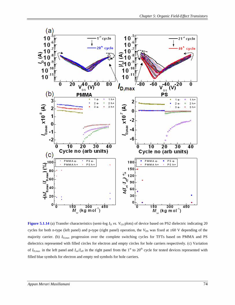
Chapter 5: Organic Field-Effect Transistors
Appan Merari Masillamani 74
Figure 5.1.14 (a) Transfer characteristics (semi-log ID vs. VGS plots) of device based on PS2 dielectric indicating 20
cycles for both n-type (left panel) and p-type (right panel) operation, the VDS was fixed at ±60 V depending of the
majority carrier. (b) ID,max progression over the complete switching cycles for TFTs based on PMMA and PS
dielectrics represented with filled circles for electron and empty circles for hole carriers respectively. (c) Variation
of ID,max in the left panel and Ion/Ioff in the right panel from the 1st to 20
th cycle for tested devices represented with
filled blue symbols for electron and empty red symbols for hole carriers.

Chapter 5: Organic Field-Effect Transistors
Appan Merari Masillamani 75
Note that majority of the devices with varying Mw of dielectrics exhibited a more positive or
negative ΔVON shift operating in n-channel or p-channel mode respectively with the exception of
PS1. The ΔVON instability over extended cycles of operation is attributed to the slow trapping at
the dielectric/semiconductor interface and dielectric surface charging effects.6,48
Some carriers
become immobile by the initial filling up of shallow trap levels when the gate bias is below the
threshold regime and after the critical threshold potential more number of the carriers become
mobile as seen by the rise in the ID (Figure 5.1.14a), when this process is repeated many number
of times the evolution of the dielectric polarization effect on the device characteristics becomes
apparent. Figure 5.1.14b shows the progression of the maximum current for each cycle of
operation for devices based on PMMA and PS dielectrics at all Mw. On close inspection of the
change in ID,max with successive cycles there is a clear steady decay of the current, this is likely
due to the slow formation of bipolaron electronic states in the F8BT layer.49
The major twofold
effect of bias stress in polyfluorenes50
which causes shifts in VON and diminution of the current
has been proposed to be caused by hole paired bipolarons which self-traps charges.
We believe the primary cause of the decay of the ID in our devices is due to the formation of
bipolaron electron or hole paired states within the F8BT film, since (1) the gradual decay of the
current strongly suggests the capture of free carriers in a tightly bound electronic state of poor
mobility and (2) irrespective of the dielectric in the device this behavior was persistent. To
validate the bias stress effect due to charge trapping according to the bipolaron model,50
we
plotted the square of the electron concentration (Ne2) against its corresponding rate of decrease
with time (dNe/dt). The near linear decrement of the carrier concentration with respect to Ne2
within experimental uncertainties is shown in Figure 5.1.15a for device based PS2 dielectric,
gives a good indication that one of the major cause of the bias stress in these devices are due to
bipolarons. A similar graph was plotted for the case when the transistor was operating in p-
channel mode from which the rate constant for hole carriers was estimated from the slope of the
linear least squares fitting of Nh2 vs. dNh/dt (Figure 5.1.15b). The respective rate constants for
electrons (re) and holes (rh) for a device based on PS2 dielectric was found to be ~1.6 x10⁻¹⁹
cm2/s and ~2.1 x10
-20 cm
2/s.

Chapter 5: Organic Field-Effect Transistors
Appan Merari Masillamani 76
Figure 5.1.15 The rate of decrease of carrier concentration vs. square of the respective carrier concentration
measured at varying time illustrated for (a) electrons at a VGS of 60 V and (b) holes at a VGS of -60 V.
On closer observation of the channel current it is apparent that there is a much larger decay of
hole current than the electron current for devices comprising of both dielectrics in all Mw scales,
this is attributed to the larger rate constant for holes than electrons as estimated for the transistor
with PS2 dielectric to be ~8. Note that the current decay in p-channel devices where much
greater than n-channel ones, this is believed to be due to (1) larger hole injection barrier to the
HOMO than electron injection barrier with the LUMO, and (2) More trapping of holes by
bipolaron hole pairs than that of electrons and consequently larger rate constants. It is also likely
that upon successive forward-reverse gate potential traces the carrier concentration injected into
the channel increases and this can lead to overcharging within the polymer semiconductor51
resulting in reduction of conductivity.
The variation in Ion to Ioff over several cycles of operation exhibited the opposite trend to ΔID,max
while increasing the molecular weights of polymer dielectric. In general the ΔIon/Ioff lowered or
remained constant from the first cycle of operation to the 20th
cycle of operation, Figure 6c
shows the variation of Ion/Ioff over several cycles of operation for all the molecular weights of
both the dielectrics employed in this study. We believe that the improved stability of the Ion/Ioff
over continuous switching OTFT operation for devices with comprising of higher molecular
weight dielectric is due to the lower densities of the polymeric dielectric chain ends at the surface
of the bulk (Figure 5.1.16). Consequently the devices with higher molecular weight dielectrics
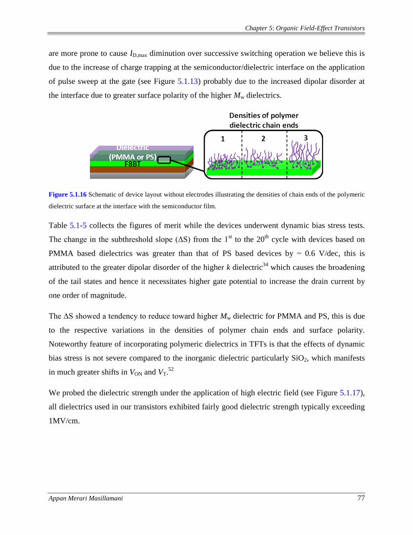
Chapter 5: Organic Field-Effect Transistors
Appan Merari Masillamani 77
are more prone to cause ID,max diminution over successive switching operation we believe this is
due to the increase of charge trapping at the semiconductor/dielectric interface on the application
of pulse sweep at the gate (see Figure 5.1.13) probably due to the increased dipolar disorder at
the interface due to greater surface polarity of the higher Mw dielectrics.
Figure 5.1.16 Schematic of device layout without electrodes illustrating the densities of chain ends of the polymeric
dielectric surface at the interface with the semiconductor film.
Table 5.1-5 collects the figures of merit while the devices underwent dynamic bias stress tests.
The change in the subthreshold slope (ΔS) from the 1st to the 20
th cycle with devices based on
PMMA based dielectrics was greater than that of PS based devices by ~ 0.6 V/dec, this is
attributed to the greater dipolar disorder of the higher k dielectric34
which causes the broadening
of the tail states and hence it necessitates higher gate potential to increase the drain current by
one order of magnitude.
The ΔS showed a tendency to reduce toward higher Mw dielectric for PMMA and PS, this is due
to the respective variations in the densities of polymer chain ends and surface polarity.
Noteworthy feature of incorporating polymeric dielectrics in TFTs is that the effects of dynamic
bias stress is not severe compared to the inorganic dielectric particularly SiO2, which manifests
in much greater shifts in VON and VT.52
We probed the dielectric strength under the application of high electric field (see Figure 5.1.17),
all dielectrics used in our transistors exhibited fairly good dielectric strength typically exceeding
1MV/cm.

Chapter 5: Organic Field-Effect Transistors
Appan Merari Masillamani 78
Figure 5.1.17 Plot showing the magnitude of electric field which the polymeric dielectrics could withstand before
occurrence of break down.
0 1 2 3
10-13
10-11
10-9
10-7
10-5
10-3
10-1
J (
A/c
m2)
E (MV/cm)
PMMA1
PS1
PMMA2
PS2
PMMA3
PS3

Chapter 5: Organic Field-Effect Transistors
Appan Merari Masillamani 79
5.1.8 Conclusions
We have shown that the effect of varying intrinsic molecular weight of the polymer dielectric on
the OTFT device performance in a single cycle of operation itself exists due to the subtle
variations in the surface energy and polarity. The tuning and modification of the dielectric
surface energy and polarity by change of the Mw comes into play by the improvement of device
power consumption efficiency manifested by lower threshold voltage required for devices with
higher Mw dielectrics. The hysteresis behavior observed in all the TFTs suggests trapping of
mobile carriers in shallow tail states. Smaller offsets between the VON and VOFF was observed for
the devices with higher Mw dielectrics which is due to the increase in the surface polarity of
PMMA and PS dielectrics going from low to higher Mw and a corresponding increase in trap
levels due to the energetic disorder at the semiconductor/dielectric interface. The influence on
the device stability particularly under dynamic bias stress was prominent and suggests a
bipolaron mechanism as its primary cause. The channel current for device operating in p-channel
condition reduced more severely compared to n-channel mode, this observed difference is
expected to be due to the greater trapping of hole than electrons as revealed by the estimated
respective rate constants. On general in most dielectric Mw the decay of the maximum drain
current was larger for devices with higher Mw dielectrics this is attributed to the greater trapping
of mobile carriers during continuous operation. However devices with higher molecular weight
dielectrics exhibited more stable ratio of Ion to Ioff which is essential for prolonged reliable device
operation. In conclusion for prolonged continuous reliable transistor operation it is preferable to
incorporate dielectrics of higher Mw.

Chapter 5: Organic Field-Effect Transistors
Appan Merari Masillamani 80
5.1.9 References
1 Forrest, S. R. The path to ubiquitous and low-cost organic electronic appliances on plastic. Nature
428, (2004).
2 Huitema, E. et al. Plastic transistors in active-matrix displays. Isscc Dig Tech Pap I 46, 380-381
(2003).
3 Baude, P. F. et al. Pentacene-based radio-frequency identification circuitry. Appl Phys Lett 82,
3964-3966, (2003).
4 Rogers, J. A. et al. Paper-like electronic displays: Large-area rubber-stamped plastic sheets of
electronics and microencapsulated electrophoretic inks. P Natl Acad Sci USA 98, 4835-4840
(2001).
5 Roberts, M. E. et al. Water-stable organic transistors and their application in chemical and
biological sensors. P Natl Acad Sci USA 105, 12134-12139, (2008).
6 Knipp, D., Street, R. A., Volkel, A. & Ho, J. Pentacene thin film transistors on inorganic
dielectrics: Morphology, structural properties, and electronic transport. J Appl Phys 93, 347-355,
(2003).
7 Yoon, M. H., Kim, C., Facchetti, A. & Marks, T. J. Gate dielectric chemical structure-organic
field-effect transistor performance correlations for electron, hole, and ambipolar organic
semiconductors. J Am Chem Soc 128, 12851-12869, (2006).
8 Park, J. H., Hwang, D. K., Lee, J., Im, S. & Kim, E. Studies on poly(methyl methacrylate)
dielectric layer for field effect transistor: Influence of polymer tacticity. Thin Solid Films 515,
4041-4044, (2007).
9 Kim, C., Facchetti, A. & Marks, T. J. Polymer gate dielectric surface viscoelasticity modulates
pentacene transistor performance. Science 318, 76-80, (2007).
10 Sun, X. et al. Interfacial Heterogeneity of Surface Energy in Organic Field-Effect Transistors.
Adv. Mater. 23, 1009-1014, (2011).
11 Singh, T. B. et al. High-Performance Ambipolar Pentacene Organic Field-Effect Transistors on
Poly(vinyl alcohol) Organic Gate Dielectric. Adv. Mater. 17, 2315-2320, (2005).
12 Yang, S. Y., Shin, K. & Park, C. E. The Effect of Gate-Dielectric Surface Energy on Pentacene
Morphology and Organic Field-Effect Transistor Characteristics. Adv. Funct. Mater. 15, 1806-
1814, (2005).
13 Peng, X. Z., Horowitz, G., Fichou, D. & Garnier, F. All-Organic Thin-Film Transistors Made of
Alpha-Sexithienyl Semiconducting and Various Polymeric Insulating Layers. Appl Phys Lett 57,
2013-2015 (1990).
14 Horowitz, G., Peng, X. Z., Fichou, D. & Garnier, F. Role of the semiconductor/insulator interface
in the characteristics of π-conjugated-oligomer-based thin-film transistors. Synthetic Metals 51,
419-424 (1992).
15 Parashkov, R. et al. All-organic thin-film transistors made of poly(3-butylthiophene)
semiconducting and various polymeric insulating layers. J Appl Phys 95, 1594-1596, (2004).
16 Facchetti, A., Yoon, M. H. & Marks, T. J. Gate dielectrics for organic field‐effect transistors: new
opportunities for organic electronics. Adv. Mater. 17, 1705-1725 (2005).
17 Effertz, C. et al. Design of Novel Dielectric Surface Modifications for Perylene Thin‐Film
Transistors. Adv. Funct. Mater. (2012).
18 Kline, R. J., McGehee, M. D., Kadnikova, E. N., Liu, J. S. & Frechet, J. M. J. Controlling the
field-effect mobility of regioregular polythiophene by changing the molecular weight. Adv.
Mater. 15, 1519-1522, (2003).
19 Nicollian, E. H., Berglund, C. N., Schmidt, P. F. & Andrews, J. M. Electrochemical Charging of
Thermal SiO[sub 2] Films by Injected Electron Currents. J Appl Phys 42, 5654-5664, (1971).
20 Chua, L. L. et al. General observation of n-type field-effect behaviour in organic semiconductors.
Nature 434, 194-199, (2005).

Chapter 5: Organic Field-Effect Transistors
Appan Merari Masillamani 81
21 Richards, T. & Sirringhaus, H. Bias-stress induced contact and channel degradation in staggered
and coplanar organic field-effect transistors. Appl Phys Lett 92, 023512-023513, (2008).
22 Gelinck, G. H. et al. Flexible active-matrix displays and shift registers based on solution-
processed organic transistors. Nat Mater 3, 106-110, (2004).
23 Owens, D. K. & Wendt, R. C. Estimation of the surface free energy of polymers. J. Appl. Polym.
Sci. 13, 1741-1747, (1969).
24 Zheng, Z. J. et al. Uniaxial alignment of liquid-crystalline conjugated polymers by
nanoconfinement. Nano Lett 7, 987-992, (2007).
25 Kajii, H., Koiwai, K., Hirose, Y. & Ohmori, Y. Top-gate-type ambipolar organic field-effect
transistors with indium-tin oxide drain/source electrodes using polyfluorene derivatives. Org
Electron 11, 509-513, (2010).
26 Zaumseil, J., Donley, C. L., Kim, J. S., Friend, R. H. & Sirringhaus, H. Efficient Top-Gate,
Ambipolar, Light-Emitting Field-Effect Transistors Based on a Green-Light-Emitting
Polyfluorene. Adv. Mater. 18, 2708-2712, (2006).
27 Snaith, H. J., Arias, A. C., Morteani, A. C., Silva, C. & Friend, R. H. Charge Generation Kinetics
and Transport Mechanisms in Blended Polyfluorene Photovoltaic Devices. Nano Lett 2, 1353-
1357, (2002).
28 Kim, Y. et al. Effect of electron-transport polymer addition to polymer/fullerene blend solar cells.
Synthetic Metals 152, 105-108, (2005).
29 Westenhoff, S. et al. Charge Recombination in Organic Photovoltaic Devices with High Open-
Circuit Voltages. J Am Chem Soc 130, 13653-13658, (2008).
30 Cheng, X. et al. Controlling Electron and Hole Charge Injection in Ambipolar Organic Field‐Effect Transistors by Self‐Assembled Monolayers. Adv. Funct. Mater. 19, 2407-2415 (2009).
31 de Boer, B., Hadipour, A., Mandoc, M. M., van Woudenbergh, T. & Blom, P. W. M. Tuning of
Metal Work Functions with Self-Assembled Monolayers. Adv. Mater. 17, 621-625, (2005).
32 Kim, J. S., Friend, R. H. & Cacialli, F. Surface energy and polarity of treated indium-tin-oxide
anodes for polymer light-emitting diodes studied by contact-angle measurements. J Appl Phys 86,
2774-2778 (1999).
33 Horowitz, G. Organic field-effect transistors. Adv. Mater. 10, 365-377 (1998).
34 Veres, J., Ogier, S. D., Leeming, S. W., Cupertino, D. C. & Khaffaf, S. M. Low-k insulators as
the choice of dielectrics in organic field-effect transistors. Adv. Funct. Mater. 13, 199-204 (2003).
35 Yan, H. et al. A high-mobility electron-transporting polymer for printed transistors. Nature 457,
679-U671, (2009).
36 Watts, B., Schuettfort, T. & McNeill, C. R. Mapping of Domain Orientation and Molecular Order
in Polycrystalline Semiconducting Polymer Films with Soft X-Ray Microscopy. Adv. Funct.
Mater. 21, 1122-1131, (2011).
37 Richards, T., Bird, M. & Sirringhaus, H. A quantitative analytical model for static dipolar
disorder broadening of the density of states at organic heterointerfaces. J Chem Phys 128,
234905, (2008).
38 Klauk, H. Organic electronics : materials, manufacturing and applications. (Wiley-VCH, 2006).
39 Singh, T. B. et al. Nonvolatile organic field-effect transistor memory element with a polymeric
gate electret. Appl Phys Lett 85, 5409-5411 (2004).
40 Gu, G., Kane, M. G., Doty, J. E. & Firester, A. H. Electron traps and hysteresis in pentacene-
based organic thin-film transistors. Appl Phys Lett 87, (2005).
41 Baeg, K.-J., Noh, Y.-Y., Sirringhaus, H. & Kim, D.-Y. Controllable Shifts in Threshold Voltage
of Top-Gate Polymer Field-Effect Transistors for Applications in Organic Nano Floating Gate
Memory. Adv. Funct. Mater. 20, 224-230, (2010).

Chapter 5: Organic Field-Effect Transistors
Appan Merari Masillamani 82
42 Naber, R., Bird, M. & Sirringhaus, H. A gate dielectric that enables high ambipolar mobilities in
polymer light-emitting field-effect transistors. Appl Phys Lett 93, 023301-023303 (2008).
43 Sze, S. M. Physics of semiconductor devices. 2nd edn, (Wiley, 1981).
44 Rolland, A., Richard, J., Kleider, J. P. & Mencaraglia, D. Electrical-Properties of Amorphous-
Silicon Transistors and Mis-Devices - Comparative-Study of Top Nitride and Bottom Nitride
Configurations. J Electrochem Soc 140, 3679-3683 (1993).
45 Kalb, W. L. & Batlogg, B. Calculating the trap density of states in organic field-effect transistors
from experiment: A comparison of different methods. Phys. Rev. B. 81, 035327 (2010).
46 The OFF and ON states are referred to the conditions when the drain current (ID) due to the
majority carries are minimum and maximum respectively.
47 The number of ID vs. VGS forward and reverse traces in this experiment was terminated at 20
cycles each first for the device with n-channel followed by the p-channel. The number of cycles
recorded was manipulated by a custom developed software code.
48 Gundlach, D. et al. High mobility n-channel organic thin-film transistors and complementary
inverters. J Appl Phys 98, 064502-064508 (2005).
49 Fung, M. et al. Distinct interfaces of poly (9, 9-dioctylfluorene-co-benzothiadiazole) with cesium
and calcium as observed by photoemission spectroscopy. J Appl Phys 94, 5763-5770 (2003).
50 Street, R., Salleo, A. & Chabinyc, M. Bipolaron mechanism for bias-stress effects in polymer
transistors. Phys. Rev. B. 68, 085316 (2003).
51 Paulsen, B. D. & Frisbie, C. D. Dependence of Conductivity on Charge Density and
Electrochemical Potential in Polymer Semiconductors Gated with Ionic Liquids. J. Phys. Chem.
C 116, 3132-3141 (2012).
52 Salleo, A. & Street, R. A. Light-induced bias stress reversal in polyfluorene thin-film transistors.
J Appl Phys 94, 471-479, (2003).
Chapter 5: Organic Field-Effect Transistors
Appan Merari Masillamani 83
5.2 INTRINSIC CHARGE TRANSPORT IN POLYMERIC SEMICONDUCTOR/PHOTOCHROMIC MOLECULAR BLEND OFETS
In this section the charge transport properties in a bicomponent system comprising of the
polymeric semiconductor blended with a photochromic molecule in the active layer of an organic
field effect transistor is reported. The focus of this work was to estimate the activation energy,
intrinsic mobility and the temperature dependence of field effect transistors based on a
photochromic diarylethene (DAE) small molecule embedded in a poly(3-hexylthiophene)
(P3HT). The property of diarylethene to undergo transition from a ring opened to closed
conformational state upon ultraviolet light irradiation was exploited to probe the properties of the
transistor in both these distinct operating bistable modes.
5.2.1 Motivation
While dealing with a system of a blended materials incorporated as the active layer of the device
the intrinsic carrier mobility can be significantly affected by parameters such as,
(i) Morphological orientation of the molecules on the channel,
(ii) Energetic mismatch in the charge transport levels and the disorder caused thereof in the
blend,
(iii) Substrate wettability, affinity and phase separation effects,
(iv) Charge localization in the bulk and
(v) Grain boundaries in the film.
All of the aforementioned properties affect the carrier mobility in some form or another either by
selectively enhancing or diminishing the performance of an OFET. To understand what would be
intrinsic mobility of the blend in the active layer of the device dependent and independent of the
gate field and the temperature it is essential to record the electrical performance of the OFET in a
cryostat. Since with the cryostat the control over a wide range of temperatures can be maintained

Chapter 5: Organic Field-Effect Transistors
Appan Merari Masillamani 84
and the electric field applied to the OFET can be controlled simultaneously by means of an
external electrometer interfaced with the cryostat.
Shown in Figure 5.2.1 is the schematic structure of the OFET characterized along with the
corresponding biasing conditions at the individual electrodes. The bistable states of DAE
molecule are represented as DAE_open and DAE_closed in accordance to the ring open and
closed structural form at the bridge of diarylethene molecule.
Figure 5.2.1 Schematic of the OFET with biasing configurations along with the chemical structure of the active
layer in the device
In the case of P3HT/DAE_open based OFET devices were characterized without any
electromagnetic wave irradiation while in the case of P3HT/DAE_closed based OFET UV
irradiation for 10 min was undertaken to transform the DAE molecules in the polymer matrix to
ring closed state.

Chapter 5: Organic Field-Effect Transistors
Appan Merari Masillamani 85
Photochromic switching mechanism 5.2.1.1
The photochromic molecules embedded in a polymeric matrix allows the possibility to tune
charge transfer energetic states between these two separate entities by means of optical
stimulation. The diarylethene molecules undergoes electrocyclization when exposed to
ultraviolet light at wavelength of 366 nm, this process closes the ring of the DAE molecule.1
Upon absorption of UV rays the excitation of an electron from the HOMO to the LUMO level
occurs (Figure 5.2.2). The initial ring open form can be recovered by subsequent irradiation with
a white light source with λ is the range of 400 to 700 nm.
Figure 5.2.2 Schematic energy diagram illustrating the switching between the bistable states of the photochromic
molecule. The change in states from A to B is triggered by external optical stimulus via the excited electronic state.
(a) When the energetic barrier is large in the ground state optical excitation is the preferred mechanism. (b) For low
energy barrier between the ground states of A and B, the reverse reaction can be triggered optically and by thermal
stimulus.
The switching process in a photochromic molecule such as diarylethene is proposed2 to follow
the steps as shown in Figure 5.2.2. The reversible opening of the ring in the bridge of the
diarylethene is likely due to multiple photon absorption involving across different intermediate
energetic states.3 This effective optical tuning of the energetic states of the diarylethene molecule
has been exploited to control current in an organic electronic device such as a field-effect
transistor.4 The light driven reversible switching behavior is realized by the change in the
electronic energetic levels and the charge distribution in the molecule.

Chapter 5: Organic Field-Effect Transistors
Appan Merari Masillamani 86
5.2.2 Results and discussions
Absorbance of spin coated blend film 5.2.2.1
To estimate the time duration necessary for irradiation with the UV light to enable the complete
transformation of the DAE_open to the DAE_closed state we performed UV/Vis absorption
characterization. The absorption spectrum was recorded after irradiation with UV light with λ of
366 nm (8 W) for time intervals of 30, 30, 60, 120 and 300 seconds respectively. Figure 5.2.3
shows the absorption spectrum of when the P3HT/DAE_open film undergoes transition to
P3HT/DAE_closed state. Prominent change in absorbance occurs at λ of 256 nm, 518 nm, 552
nm and 597 nm.
Figure 5.2.3 Absorption spectrum of spin coated blend film of P3HT and DAE_open on quartz slide. The arrows
indicate the change in the magnitude of absorbance upon successive irradiation times. The time (seconds) in the
legend indicates the interval with reference to the initial measurement.
The absorption of the film reduces and exhibits a small blue shift at λ of 552 nm and 597 nm
while at λ of 518 nm there is small red shift. On careful inspection of the absorbance spectrum, it
can be noted that after UV irradiation for ~ 540 s the majority of the photochromic DAE
molecules in the blend film adopt closed state configuration. Hence we decided to irradiate the
spin casted blend film for 10 min to allow the DAE molecules to metamorphose from the open to
closed state.

Chapter 5: Organic Field-Effect Transistors
Appan Merari Masillamani 87
Temperature dependence of transport in OFETs based on P3HT/DAE blend 5.2.2.2
The electrical characterization was performed on a device with channel length (L) of 20 µm and
a channel width (W) of 10000 µm. The employed device geometry was of bottom-gate bottom-
contact configuration. The surface of the SiO2 dielectric layer was kept in its pristine state prior
to deposition of the semiconducting thin film; this allowed us to examine the intrinsic charge
transport properties of the blend film. In the case of P3HT/DAE_open based OFET devices were
characterized without any electromagnetic wave irradiation while in the case of
P3HT/DAE_closed based OFET UV irradiation for 10 min was undertaken to transform the
DAE molecules in the polymer matrix to its closed form.
The transfer characteristics (drain current, ID versus gate bias, VGS) of transistors based on
predominantly hole carrier transporting (p-type) P3HT/DAE blend films were acquired from 80
K to 300 K in intervals on 20 K. Once the OFET was housed inside the cryostat, prior to starting
measurements at different temperatures a single ID - VGS measurement was recorded to ensure the
integrity and the stability of the electrical contact.
Figure 5.2.4 Transfer characteristics for the P3HT/DAE blend based OFET when the DAE molecule was in the (a)
open state and (b) ring closed state. The VDS was held at -10 V while the gate bias was swept.
Shown in Figure 5.2.4 a and b are the ID - VGS response of the OFET in the linear regime for
different temperatures. For acquiring the transfer characteristic the gate bias was sourced starting
from +40 V → -60 V and the drain current was measured at 2 V intervals, while the drain bias
was held fixed at a low bias (-10 V) and higher bias (-60 V) for each complete gate bias sweep.

Chapter 5: Organic Field-Effect Transistors
Appan Merari Masillamani 88
The semi-log plots of ID - VGS for the OFET based on P3HT with DAE in open or closed forms is
shown in Figure 5.2.5. From the Figure 5.2.5 the temperature dependence of the blend can be
clearly visualized. The temperature dependent variation in drain current gives rise to
corresponding dependence of hole mobility.
Figure 5.2.5 Semi-log plots of ID-VGS clearly illustrating the variation of linear regime drain current (VDS = -10
V)with temperature for OFET with (a) P3HT/DAE_open and (b) P3HT/DAE_closed molecules in the active layer.
The hole carrier mobility can be estimated in the linear regime from the drain current
dependence on the gate bias by equation 5.2.1,5
W
L
VVVC
IVT
amb
TGSDSi
DGSlin .),(
(5.2.1)
Where Ci is the gate dielectric capacitance and amb
TV is the gate voltage at which the device
strongly turns on (i.e, where the ID starts to rise) extracted at ambient temperature. In our
experiment the amb
TV remained fairly constant and not shift over different temperatures. The amb
TV
values where thus estimated when the ID started to increase from its minimal value for the
P3HT/DAE_open and closed to be +10.25 V and +17.72 V respectively. Then using equation
5.2.1 the linear mobility was estimated as a function of both temperature and gate bias. Shown in
Figure 5.2.6 are the linear regime hole mobility across different temperature and the gate bias
range. Note the increase at most temperatures mobility with the gate field suggests the shift in
the Fermi level of the semiconductor blend closer the mobility edge. When the Fermi level

Chapter 5: Organic Field-Effect Transistors
Appan Merari Masillamani 89
moves near the mobility edge more number of carriers is localized near the valence band edge
and thus there are more mobile carriers which contribute to the charge transport. At lower gate
bias the Fermi level is likely further away from the valence band edge where some charges can
be trapped in deep immobile states which consequently lower the hole mobility.
Figure 5.2.6 Semi-log plots of hole carrier mobility in the linear regime as a function of temperature and gate field
for OFET with (a) P3HT/DAE_open and (b) P3HT/DAE_closed molecules in the active layer.
The variation in hole carrier mobility depending on temperature also suggest that there exists a
thermally activated behavior. Upon inspection of the variation of hole mobility with temperature
for we can observe that the variation of hole mobility with temperature is much higher for
devices comprising of P3HT/DAE_open molecules as the semiconducting film suggested that
the thermal activation is slightly higher in this case. The increase in hole mobility with
temperature can be attributed to the activation energy, which is the energy required to the move
the charges localized in immobile states to hop mobile states. The activation energy can be
estimated from the Arrhenius relationship of mobility with temperature as shown in equation
5.2.2.6,7
Tk
E
B
alin exp0 (5.2.2)
Where Ea is the activation energy,8 KB is Boltzmann constant (8.617 x10
-5 eV K
-1), T is absolute
temperature and µ0 is the prefactor mobility which is a mobility at infinite temperature. Figure

Chapter 5: Organic Field-Effect Transistors
Appan Merari Masillamani 90
5.2.7 and Figure 5.2.8 show the variation of mobility with temperature at different fixed gate bias
values for devices based on P3HT with DAE_open or closed films.
Figure 5.2.7 Arrhenius plot showing the linear mobility as function of temperature at different fixed gate bias values
for OFET with P3HT/DAE_open blend in active layer.
For the P3HT/DAE_open device there is thermally activated hopping behavior from 300 K to
100 K below which there is weak dependence of charge transport which suggests tunneling
between localized states. In the case of transistor based on P3HT/DAE_closed semiconductor
film there is strong dependence of charge transport with temperature from 280 K to 80 K. On
close observation from the Arrhenius plots of carrier mobility as a function of inverse
temperature besides the onset temperature of thermal activation, there is major differences in the
profile of the change in hole mobility with temperature and gate bias. For instance, the slope of
the linear fits to the µlin vs. 1/T plot for P3HT/DAE_open is much steeper in comparison to that
of P3HT/DAE_closed based device which manifests as greater levels of activation energy
required to promote carrier hopping.

Chapter 5: Organic Field-Effect Transistors
Appan Merari Masillamani 91
Figure 5.2.8 Arrhenius plot showing the linear mobility as function of temperature at different fixed gate bias values
for OFET with P3HT/DAE_closed blend in active layer.
The activation energy as a function of gate bias is shown in Figure 5.2.9. As expected the
activation energy shows an exponential decrease with increase in the gate bias, this again
supports the fact that the Fermi level shifting closer the valence band edge of the blend film.5,9
The greater activation energy of the device with P3HT/DAE_open with respect to the
P3HT/DAE_closed based device can be attributed to the higher energetic mismatch between the
P3HT and the DAE molecule in its open form. The Ea ranges from ~280 to 120 K as the gate bias
approaches -60 V for the P3HT/DAE_open FET while for P3HT/DAE_closed it varies from
~110 to 75 eV. The much larger activation energy comported for the device with DAE_open
molecule in the P3HT blend is attributed to the significant energetic barrier imposed between the
respective ionization energy (IE) levels these compounds in its pristine form.4
The IE values determined by means of ultraviolet photoelectron spectroscopy for P3HT,
DAE_open and closed molecules were reported to be ~4.4 to 4.9, 5.1 and 5.7 eV respectively
(Figure 5.2.10).4,10
For P3HT the reported IE values in the literature measured by means of cyclic
voltammetry was 4.8 eV.4

Chapter 5: Organic Field-Effect Transistors
Appan Merari Masillamani 92
Figure 5.2.9 Activation energy as a function of gate bias for OFET based on (a) P3HT/DAE_open and (b)
P3HT/DAE_closed semi-conductive film in the active layer.
The energetic barrier becomes apparent if we represent the IE values of the individual
compounds of the bicomponent semiconductor film on a common energetic scale.
Figure 5.2.10 Illustration of the ionization energy levels of DAE small molecules in both open and closed forms
along with P3HT. The IE offset between the P3HT and DAE isomers is depicted. The + symbol inside a circle
represents the hole carrier barrier between the P3HT and DAE in open and closed forms respectively.
If we consider variable range hopping of hole carriers within a Gaussian density of states (DOS),
the mobility shows a dependence with the 1/T2
from which the width of the DOS ( DOS ) can be
estimated,7,11,12

Chapter 5: Organic Field-Effect Transistors
Appan Merari Masillamani 93
2
2
5.0
2
0 exp3
2exp
TKCE
TK B
DOS
B
DOS (5.2.3)
Where KB is Boltzmann constant, µ0 is the prefactor mobility which occurs in the case if there is
no energetic disorder when T , E is the applied gate electrical field and describes the
extent of spatial disorder.
Due to the very low lateral field applied to our devices E 5 kV/cm, the Poole-Frenkel like
second exponential term in equation 5.2.3 can be neglected. Thus the description of the carrier
mobility in terms of Gaussian disorder model can be written as,
2
03
2exp
TKB
DOS (5.2.4)
Figure 5.2.11 Non Arrhenius plot with linear hole Mobility vs. inverse square of temperature for transistor with
semiconductor film comprising of P3HT blended with (a) DAE_open and (b) DAE_closed molecules.
The change in mobility with respect to the inverse of the square of temperature for devices with
DAE in both its isomeric forms blended with P3HT is shown in Figure 5.2.11. The DOS
estimated amounts to ~70 and 38 meV for transistors with P3HT mixed with DAE_open and
closed forms respectively.

Chapter 5: Organic Field-Effect Transistors
Appan Merari Masillamani 94
The larger standard deviation of the Gaussian DOS for the FET based on P3HT/DAE_open by a
factor >1.8 affirms the greater amount of ionization energetic disorder in the blend when P3HT is
blended with DAE_open as opposed to DAE_closed molecule, if we consider the separate IE
values as a reference. Another way to view this aspect is, the charge requires much more energy
to perform hops from one energetic site to another as it travels along the channel composed of
P3HT/DAE_open molecules. In essence the large offset existing between the IE levels of the
DAE_open with respect to the P3HT makes its much more difficult for hole carrier hopping than
the lower offset which is required to perform charge hopping along the P3HT/DAE_closed film.
More crucially the DOS of 38 meV for the P3HT/DAE_closed is lower than the pristine P3HT
FET of 45 meV reported in literature,7 this suggests that the addition of DAE_closed molecule to
the P3HT film does not significantly cause diagonal energetic offset disorder in the bulk. This is
probably due to the arrangement of the small DAE molecules in the amorphous regions of the
P3HT matrix.4
5.2.3 Conclusions
The activation energy required for charge hopping in transistors based on P3HT and DAE_open
molecules is atleast a factor of two greater than for P3HT/DAE_closed active layer. The higher
energy require to perform inter molecular hole carrier hopping in the FET channel comprising of
P3HT/DAE_open film can be directly attributed to the greater energetic offset between the
ionization energy levels of P3HT and DAE_open molecules and the contrary is true for
DAE_closed molecules in the polymeric blend. The smaller IE difference between P3HT and
DAE_closed molecules directly correlates to the narrower width of the Gaussian density of
states, of 38 meV if we consider variable range hopping as the prevalent charge transport
mechanism. Interestingly the DOS of P3HT/DAE_closed was less than that of the pristine
P3HT, which suggests that the addition of more resistive DAE_closed molecule to the P3HT
does not significantly affect the energetic disorder in the bulk of the film since its packed into the
amorphous regions of the polymeric semiconductor.

Chapter 5: Organic Field-Effect Transistors
Appan Merari Masillamani 95
5.2.4 References and notes
1 Li, J., Speyer, G. & Sankey, O. F. Conduction switching of photochromic molecules. Phys. Rev.
Lett. 93, 248302 (2004).
2 Sworakowski, J. & Lutsyk, P. Bistable organic materials in optoelectrical switches: Two-
electrode devices vs. organic field effect transistors. Ukr. J. Phys. 56, 1021-1029 (2011).
3 Goldberg, A. et al. Rotational isomerization of dithienylethenes: A study on the mechanism
determining quantum yield of cyclization reaction. J. Phys. Chem. A 107, 4982-4988 (2003).
4 Orgiu, E. et al. Optically switchable transistor via energy-level phototuning in a bicomponent
organic semiconductor. Nat Chem 4, 675-679 (2012).
5 Salleo, A. et al. Intrinsic hole mobility and trapping in a regioregular poly (thiophene). Physical
Review B 70, 115311 (2004).
6 Chesterfield, R. J. et al. Variable temperature film and contact resistance measurements on
operating n-channel organic thin film transistors. J. Appl. Phys. 95, 6396-6405 (2004).
7 Majewski, L., Schroeder, R., Grell, M., Glarvey, P. & Turner, M. High capacitance organic field-
effect transistors with modified gate insulator surface. J. Appl. Phys. 96, 5781-5787 (2004).
8 This is defined as the minimum amount of energy required to complete the charge transport
which is frequently described to occur by hopping between sites and it is expressed in units of eV
or meV.
9 Chang, J. F., Sirringhaus, H., Giles, M., Heeney, M. & McCulloch, I. Relative importance of
polaron activation and disorder on charge transport in high-mobility conjugated polymer field-
effect transistors. Physical Review B 76, 205204 (2007).
10 Masillamani, A. M. et al. Multiscale Charge Injection and Transport Properties in Self-
Assembled Monolayers of Biphenyl Thiols with Varying Torsion Angles. Chem. Eur. J. 18,
10335-10347, (2012).
11 Bässler, H. Charge Transport in Disordered Organic Photoconductors a Monte Carlo Simulation
Study. physica status solidi (b) 175, 15-56, (1993).
12 Veres, J., Ogier, S. D., Leeming, S. W., Cupertino, D. C. & Mohialdin Khaffaf, S. Low‐k
Insulators as the Choice of Dielectrics in Organic Field‐Effect Transistors. Adv. Funct. Mater. 13,
199-204 (2003).


Chapter 5: Organic Field-Effect Transistors
Appan Merari Masillamani 97
5.3 ACTIVATION ENERGY OF OFETS BASED ON QUINOIDAL OLIGOTHIOPHENE DERIVATIVE
In this part of the chapter the investigation of the intrinsic charge transport properties of
ambipolar field-effect transistors based on quinoidal oligothiophene oligomer incorporated as the
semiconducting layer in the device is investigate in detail. The quinoidal oligothiophene
derivative employed in this study undergoes changes in its morphological arrangement and
energetic profile of charge transport levels upon certain post-processing conditions such as
annealing and solvent vapor treatment. The focus of this study was to estimate the intrinsic
mobility and activation energy by mean of electrical characterization of these OFETs in a static
cryostat. The activation energy for electron charge carries (n-channel transistor operation) was
investigated for pristine spin coated and post-annealed QQT(CN)4 films.
5.3.1 Scope
The intrinsic charge transport properties in organic semiconductor films can be tuned by means
of post-processing of the deposited films.1-3
The most commonly employed method for the
deposition of the semiconductor film is by means of spin casting. This technique for deposition
has some crucial advantages such as reduced processing complexity, possibility to obtain
homogenous thickness and morphology over a wide region of the substrate and minimal duration
required to achieve good quality thin films with homogenous spread of thickness over large
areas.
One of the prominent advantages of organic materials is that once the material is deposited on
the substrate surface the morphological properties and its respective opto-electronic properties
can be tuned by means of simple post-deposition methods. Among the post-deposition
processing methods the widely employed route is by means of,
(i) Thermal annealing3 and
(ii) Solvent vapor treatment

Chapter 5: Organic Field-Effect Transistors
Appan Merari Masillamani 98
Figure 5.3.1 Structure of bottom-gate bottom-contact OFETs based on quinoidal oligothiophene derivative, shown
in the left and right panels are the hole and electron transporting transistors along with the respective biasing
configurations. Note that the as spin casted QQT(CN)4 film exhibits ambipolar behavior.
In this study we make use of thermal annealing to alter the electronic transport levels and thereby
the charge transport properties in the quinoidal oligothiophene (see Figure 5.3.1 inset) based
field-effect transistors.
5.3.2 Results and discussions
5.3.2.1 Absorption spectra of QQT(CN)4 film
The as-spun QQT(CN)4 film on quartz substrate has a broad absorption band, λ from ~790 nm to
1495 nm at full width at half maximum (fwhm). Upon annealing of the film for 180 °C for 10 s
the absorption band width becomes narrower (λ from 780 nm to 1130 nm) and more blue shifted.
Figure 5.3.2 shows the absorption profiles of the QQT(CN)4 film pre and post annealing.

Chapter 5: Organic Field-Effect Transistors
Appan Merari Masillamani 99
Figure 5.3.2 UV/Vis absorption spectrum profiles of the QQT(CN)4 film, as spun (black), annealed (blue) and
solvent vapor treated in CHCl3 after annealing (red)
The consequence of the shift in the absorption profile of the film of the QQT(CN)4 is that the
energetic band gap (HOMO-LUMO) levels change correspondingly. The HOMO level of the
drop casted QQT(CN)4 film as estimated from the ionization energy level from UPS
measurements were ~5.3 eV. After annealing the QQT(CN)4 film undergoes blue shift in
absorption resulting in increase in optical band gap and down shifting of the LUMO level to ~4.7
eV from ~4.5 eV. The LUMO levels were estimated from the recorded optical band gap from the
long absorption tail of the absorption spectrum (Figure 5.3.2). The shift in the energetic orbital
levels had been attributed to the changes in molecular packing and crystallinity for the annealed
film with respect to the spin coated one. The pertinent feature of this molecule is that, just by
thermal annealing of the film the property of the molecule in the bulk can be modified to
transport electrons converse to the initial state of majority hole carrier conduction.1,2
These
salient features enable the usage of the air stable Au electrodes for injecting both holes and
electrons, thus enabling the possibility of realizing bipolar devices based on complementary
metal-oxide semiconductor (CMOS) logic circuits.

Chapter 5: Organic Field-Effect Transistors
Appan Merari Masillamani 100
5.3.2.2 Energetic profile of electronic charge transport levels
Shown in Figure 5.3.3 is the energy band diagram of the drop casted QQT(CN)4 film as
deposited by drop casting and annealed, the work function of the injecting Au electrodes is
indicated for visualizing the energetic barrier with the corresponding molecular orbitals.
Figure 5.3.3 Energy band diagram of QQT(CN)4 film, as drop casted (maroon), annealed (blue) along with the
work function of the gold electrode as recorded by UPS.
Since the work function (Φ) of the Au electrodes (measured with UPS) was ~ 4.82 eV, the
injection barrier to the HOMO level is favorable towards p and n-type behavior while the same
film upon annealing results in the LUMO level shift closer to the Fermi level of the Au electrode
which favors electron transport (n-type). With the flexibility and versatility to the change the
intrinsic charge transport properties of the semiconducting material we aimed to investigate the
activation energy which might be required for the transistors operating in both p and n-type
operational mode. For this end we fabricated TFTs in bottom–gate bottom-contact device
geometry on a highly doped Si substrate which served as the gate electrode with a dielectric layer
of SiO2 sandwiched between the bottom gate and the top interdigitated source-drain gold

Chapter 5: Organic Field-Effect Transistors
Appan Merari Masillamani 101
electrodes. The fabrication of the device was completed upon the spin coating of 75 µl of
QQT(CN)4 solution (2 mg ml-1
in CHCl3) onto the cleaned substrates.
5.3.2.3 Electrical characterization of QQT(CN)4 OFETs in a cryostat
Device with channel length (L) of 20 µm and width (W) of 10000 µm was characterized for both
p and n-type QQT(CN)4 OFETs.
QQT(CN)4 ambipolar OFET: Device was characterized after spin casting QQT(CN)4 from
CHCl3 onto substrates with pre-patterned electrodes. The transfer characteristics for QQT(CN)4
OFET in n-type operational mode in linear regime is shown in Figure 5.3.4a.
QQT(CN)4 n-type OFET: Device was characterized after spin casting QQT(CN)4 and then a
subsequent annealing step at 150 °C for 5 s in ambient conditions.
Figure 5.3.4 Semi-log plots of ID vs. VGS for n-channel spin coated (left panel) and annealed (right panel)
QQT(CN)4 OFETs at different temperatures, the corresponding drain potential was held constant at +10V.
Depicted in Figure 5.3.4b are the transfer characteristics for QQT(CN)4 OFET in n-type
operational mode in linear regime at various temperatures.
Transfer characteristics of the OFETs were recorded from temperature range of 300 K to 80 K
for n-type and from 300 K to 120 K for ambipolar OFETs in steps of 20 K.

Chapter 5: Organic Field-Effect Transistors
Appan Merari Masillamani 102
It is interesting to note that thermal annealing of the QQT(CN)4 film causes the lowering of the
magnitude of the off drain current with respect to that recorded for device with pristine spin
coated film at similar temperature scales. While the Ion/Ioff is greater and the saturation of the
drain current is maintained which suggests clean switching behavior and no significant doping
due to moisture as in other polythiophene FETs.4 It is also likely that since the electron injection
barrier between the source electrode and the LUMO level of the annealed QQT(CN)4 film is
lower it leads to observation of increase in ID at a lower applied gate potentials, this clearly
confirms the fact of full conversion of the intrinsic charge transporting properties of the
ambipolar (electron and hole conducting) pristine spin casted QQT(CN)4 film to a pure electron
conducting n-type semiconductor. Moreover the subthreshold slope of the FET based on
annealed QQT(CN)4 film is lower than that of the bare spin coated semiconductor.
For majority of the temperature the drain current (ID) increases with rise in temperature. The
effective mobility (µeff) which describes the mobility considering the mobile and immobile
charge carriers was calculated from the linear regime.
The µlin was estimated using assuming that (i) The onset voltage (Von) is close to 0 and (ii) Von is
independent of temperature.5 The increase in ID causes a corresponding increase in mobility
which suggests an activated behavior of charge transport depending on temperature.
W
L
VVVC
ITV
onGSDSi
DGSeff .,
(5.3.1)
W
L
VVC
ITV
GSDSi
DGSlin .),( (5.3.2)
The point by point electron mobility varying with the gate potential was determined in the linear
regime from equation 5.3.2 and is depicted in Figure 5.3.5. Similar to the variation of the ID
modulation with VGS the mobility also reflects the change with respect to gate potential and
temperature.

Chapter 5: Organic Field-Effect Transistors
Appan Merari Masillamani 103
On close observation of the influence of temperature on the mobility it is apparent that there is a
much larger amount of thermally activation of charge transport for transistor based on annealed
QQT(CN)4 film.
Figure 5.3.5 Effective mobility as a function gate bias and temperature for the QQT(CN)4 TFTs under n-channel
operation for (a) spin coated film (b) annealed film after spin casting.
The variability of effective mobility with respect to gate field and temperature suggests that the
relation between exponential of activation energy and field-effect mobility by the following
equation,6
Tk
E
B
aeff exp0 (5.3.3)
Where Ea is the activation energy, kB is the Boltzmann constant, T is the absolute temperature
and µ0 is the prefactor.
For n-type semiconductor the activation energy is the offset in energy between the conduction
band edge (Ec) and the discrete trap state (ET) when the Ea is greater than the width of the trap
distribution7 and this can be expressed according to the Arrhenius relation and represented
graphically as in Figure 5.3.6,

Chapter 5: Organic Field-Effect Transistors
Appan Merari Masillamani 104
Tk
EE
B
Tceff exp0 (5.3.4)
Figure 5.3.6 Arrhenius plot showing linear regime mobility variation with temperature for n-channel QQT(CN)4
based OFET for gate bias from +10 V to +60 V, at a constant VDS of +10 V (a) spin coated film and (b) Post
annealed film after spin coating.
On close observation of the variation of mobility with temperature for the devices without or
with annealed QQT(CN)4 film as the active layer in the semiconductor we can observe clear
difference in temperature dependent activation in charge transport among these two. The first
major difference is that the change in mobility with temperature is much lower for the device
with QQT(CN)4 spin cast film than the post-annealed film device, in other words the slope of the
device with annealed film is much larger in magnitude than the device comprising of the spin
coated film. This is likely due to the greater amount of trap densities at the
dielectric/semiconductor interface, since the untreated surface of the SiO2 dielectric in these
devices which comprises of hydroxyl groups can act as effective electron trap sites8 and as a
consequence which the Ea of the n-channel only QQT(CN)4 based FET is greater. Secondly,
there are two distinct regime of temperature activation for the device comprising of the spin
casted film. Thirdly the onset of thermal activation is much higher for the device with the
annealed film, starting from ~300 K whereas for the device pristine spin coated semiconductor

Chapter 5: Organic Field-Effect Transistors
Appan Merari Masillamani 105
film it starts ~200 K. All of these factors suggest that the post processing plays a major role of
modifying the intrinsic charge transport properties of the semiconductor layer.
Figure 5.3.7 The point by point activation energy as a function of the gate bias for transistors based on film of
pristine spin casted and annealed QQT(CN)4 semiconductor film at n-channel operation condition.
To probe these fact we extrapolated the activation energy for QQT(CN)4 based device operating
in n-channel mode with or without annealing. The activation energy calculated for each of the
gate potential for the QQT(CN)4 transistor operation in n-channel mode is shown in Figure
5.3.7.
The lower activation energy at higher gate fields suggest that the accumulated charges in the
channel will occupy higher energy sites closer to the conduction band mobility edge,3,7 wherein
lesser energy would be required to activated hopping to neighboring sites. Coincidentally the Ea
ranges from ~220 to 38 meV and ~93 to 56 meV with increasing gate voltages for the transistor
with annealed and spin coated films respectively.
If we assume that the density of electronic states (DOS) of the carriers is distributed randomly, it
can be described according to a Gaussian profile proposed by Bässler.9 Alternatively the density
of states in the band gap is considered to be exponentially distributed. A unified description of
these two models was suggested by Tanase and co-workers where they show that in FETs with
conjugated semiconductor structures when the magnitude of the areal charge density is large the
0 10 20 30 40 50 600
50
100
150
200
250
VGS
(V)
annealed
as spun
Ea (
meV
)

Chapter 5: Organic Field-Effect Transistors
Appan Merari Masillamani 106
exponential DOS is a reasonable approximation of Gaussian DOS.10
The width of the Gaussian
density of states, DOS extrapolated at T0 of ~ 191 K for amounts to 67 meV which lies within
the energy range of annealed QQT(CN)4 FET.
Similarly the DOS of spin coated QQT(CN)4 transistor was estimated to be 37 meV at a T0 of ~
109 K which lies within its Ea range from 93 to 56 meV. The dependence of mobility with
inverse square of temperature as described by the Gaussian disorder model6,9
is plotted in Figure
5.3.8.
Figure 5.3.8 Mobility as a function of inverse T2 according to the Gaussian disorder model for QQT(CN)4 FET with
(a) spin coated and (b) annealed films.
The prefactor is furthermore related to the Ea by the following empirical relation,11
isoB
a
Tk
Eexp000 (5.3.5)
Substituting equation 5.3.5 in 5.3.3 yields the following relationship,12
isoBB
aeffTkTk
E11
exp00 (5.3.6)
Where µ00 is the compensation factor which increases exponentially with rise in Ea according to
Meyer-Neldel rule (MNR) and the isokinetic temperature Tiso is related to the Meyer-Neldel

Chapter 5: Organic Field-Effect Transistors
Appan Merari Masillamani 107
energy, EMN = kB Tiso. In other words the EMN is the energy estimated at a single crossing point of
different Ea at the isokinetic temperature, which is obtained by plotting the prefactor µ0 against
the activation energy. We did not observe an intersection of prefactor mobility for the n-channel
spin coated QQT(CN)4 FET when the mobility was extrapolated to 1/T=0, however for the
transistor comprising of the annealed film a common intersection point was observed. The
variation of the µ0 spanned several orders of magnitude with respect to Ea as shown in Figure
5.3.9. The Meyer-Neldel energy at the isokinetic temperature of 807 K was estimated to be ~70
meV.
Figure 5.3.9 Prefactor µ0 as a function of Ea for n-channel annealed QQT(CN)4 FET
The origin of the MNR is consistent with a charge hopping as the mechanism of transport.13
It is
likely that the annealed film has more defect sites at the grain boundaries of microcrystalline
domains as opposed to the neat spin coated film2 hence the compensation of prefactor satisfies
the MNR well.
5.3.3 Conclusions
The temperature dependence of charge transport in QQT(CN)4 transistors operating in n-channel
mode for two different preparation conditions investigated. The transistor with the annealed
QQT(CN)4 film exhibited a much higher activation energy than the spin casted one, which could
be attributed to the presence of greater number of energetic defects sites and grain boundary
0.00 0.05 0.10 0.15 0.20 0.2510
-3
10-2
10-1
100
Ea (eV)
pre
facto
r
0 (
cm
2/V
s)

Chapter 5: Organic Field-Effect Transistors
Appan Merari Masillamani 108
disorders in the film. For the annealed device there was a strong thermally activated behavior
below 300 K and for the as spun device strong variation in mobility commenced from 200K. The
charge transport seems to follow a hopping behavior between localized trap states. The width of
the Gaussian DOS lied within the activation energy range for both transistors with or without
annealing highlighting the strong dependence of mobility with the density of charge carriers. The
Meyer-Neldel rule was obeyed by annealed film QQT(CN)4 field-effect transistor.
5.3.4 References
1 Ribierre, J. C. et al. Direct Laser Writing of Complementary Logic Gates and Lateral p–n Diodes
in a Solution-Processible Monolithic Organic Semiconductor. Adv. Mater. 22, 1722-1726 (2010).
2 Ribierre, J. C. et al. Reversible Conversion of the Majority Carrier Type in Solution‐Processed
Ambipolar Quinoidal Oligothiophene Thin Films. Adv. Mater. 22, 4044-4048 (2010).
3 Salleo, A. et al. Intrinsic hole mobility and trapping in a regioregular poly (thiophene). Phys. Rev.
B 70, 115311 (2004).
4 Hoshino, S. et al. Influence of moisture on device characteristics of polythiophene-based field-
effect transistors. J. Appl. Phys. 95, 5088-5093 (2004).
5 Chang, J. F., Sirringhaus, H., Giles, M., Heeney, M. & McCulloch, I. Relative importance of
polaron activation and disorder on charge transport in high-mobility conjugated polymer field-
effect transistors. Phys. Rev. B 76, 205204 (2007).
6 Majewski, L., Schroeder, R., Grell, M., Glarvey, P. & Turner, M. High capacitance organic field-
effect transistors with modified gate insulator surface. J. Appl. Phys. 96, 5781-5787 (2004).
7 Chesterfield, R. J. et al. Variable temperature film and contact resistance measurements on
operating n-channel organic thin film transistors. J. Appl. Phys. 95, 6396-6405 (2004).
8 Chua, L. L. et al. General observation of n-type field-effect behaviour in organic semiconductors.
Nature 434, 194-199 (2005).
9 Bässler, H. Charge Transport in Disordered Organic Photoconductors a Monte Carlo Simulation
Study. Phys. Status Solidi B 175, 15-56, (1993).
10 Tanase, C., Meijer, E., Blom, P. & De Leeuw, D. Unification of the hole transport in polymeric
field-effect transistors and light-emitting diodes. Phys. Rev. Lett. 91, 216601 (2003).
11 Meyer, W. & Neldel, H. Relation between the energy constant and the quantity constant in the
conductivity–temperature formula of oxide semiconductors. Z. tech. Phys 18, 588-593 (1937).
12 Meijer, E. J., Matters, M., Herwig, P. T., de Leeuw, D. M. & Klapwijk, T. M. The Meyer--Neldel
rule in organic thin-film transistors. Appl. Phys. Lett. 76, 3433-3435 (2000).
13 Horowitz, G., Hajlaoui, M. E. & Hajlaoui, R. Temperature and gate voltage dependence of hole
mobility in polycrystalline oligothiophene thin film transistors. J. Appl. Phys. 87, 4456-4463
(2000).

Chapter 5: Organic Field-Effect Transistors
Appan Merari Masillamani 109
5.4 IMPROVED FIELD-EFFECT MOBILITY IN A POLYMERIC SEMICONDUCTOR/SMALL MOLECULAR BLEND TRANSISTORS
In this part the influence of blending a thiophene based small molecule with a polymeric
semiconductor and incorporated as the charge transport layer in field-effect transistor is reported.
The focus of this project was to determine the effect of varying ratios of 5,5’-bis(4-n-
hexylphenyl)-2,2’-bithiophene (dH-PTTP) by weight in a poly(3-hexylthiophene) (P3HT)
mixture deposited as the active layer of FETs on the hole carrier mobility. The relation between
the electronic and morphological ordering of the molecules was systematically investigated.
Possible correlations between the enhancements of mobility at certain blend films and phase
segregation effects are discussed.
5.4.1 Prospects
Organic thin-film transistors (OTFTs) are attracting a great attention as promising candidates for
cheap, flexible and large-area electronics.1-8
In particular, the use of solution-deposited polymers
featuring semiconducting properties represents a valid alternative to amorphous silicon, with the
advantage of a versatile processability using ink-jet printing/roll-to-roll techniques which are
suitable for the mass production of low-cost electronics. In this regard, poly(3-hexylthiophene)
(P3HT) is a prototypical p-type polymer that combines a good solubility in numerous organic
solvents with large field-effect mobilities in thin films.9 However the semi crystalline nature of
the polymer based assemblies limits their electrical characteristics. On the other hand, small
molecules, which typically exhibit greater mobilities,10,11
suffer from problems related to their
tendency to aggregate forming microscopic crystals. These crystals cannot be easily interfaced to
metallic electrodes, limiting charge injection at metal-semiconductor interfaces, and are
characterized by grain boundaries, which negatively affect the charge transport within the film.
For this reason, blends of polymer/small molecule are used in all those applications where
multiple requirements are necessary and cannot be fulfilled by employing a single component.
Mobilities measured upon blending two p-type components exhibited improved charge transport
characteristics over the starting mobilities of the single components.12-16

Chapter 5: Organic Field-Effect Transistors
Appan Merari Masillamani 110
5.4.2 Results and discussions
Here we show that the mobility within a P3HT based OTFT film can be increased by co-
deposition with 5,5’-bis(4-n-hexylphenyl)-2,2’-bithiophene (dH-PTTP) (Figure 5.4.1), a small
molecule that displayed in the past interesting charge transport properties in organic transistors
and volatile memories.17-19
Significantly, we have found that a field-effect mobility of ~ 0.1
cm2V
-1s
-1 can be achieved upon modulating the ratio of the two components in the blend, with the
highest value measured in 1:1 blends of P3HT:dH-PTTP in weight ratio. Such a mobility is about
10-fold higher than the mobility measured in bare P3HT films, and about 50-fold greater than
those measured in bare dH-PTTP films. Furthermore, ultraviolet ambient photoelectron
spectroscopy technique is employed to monitor the work-function variation of the blend upon
changing the two components ratio, providing a reliable means to evaluate the vertical phase-
segregation process that has been found to characterize polymer/small molecule systems.20
5.4.2.1 Electrical characterization of P3HT:PTTP OFETs
Transistors in bottom-contact bottom-gate configuration were fabricated on n++
- Si substrates
with 230 nm of thermally grown SiO2 as the gate dielectric and pre-patterned pairs of gold
electrodes with interdigitated geometry as the source and drain. The semiconductor layer was
deposited by drop-casting from a 5 mg/ml solution in p-xylene.
Figure 5.4.1 Schematic illustration of OTFT structure (bottom contact) and the chemical structures of PTTP (5,5’-
bis(4-n-hexylphenyl)-2,2’-bithiophene, P3HT (poly(3-hexylthiophene))
Samples having different ratio in weight were prepared, comprising ratios spanning from 0% of
dH-PTTP, i.e. pure P3HT, to 100% of dH-PTTP. The range included 5%, 25%, 50%, 75% and
95%. After drop-casting, films were dried up at room temperature overnight.

Chapter 5: Organic Field-Effect Transistors
Appan Merari Masillamani 111
All samples were prepared and measured in a N2 filled glovebox to avoid oxidative doping of the
materials and ensure reproducibility of the experiments. It is worth noting that differently from
other works12,20
i) drop-casting was chosen as the deposition technique since it is more similar, if
compared to spin-coating, to the ink-jet printing process used in real device fabrication; ii) no
electrode treatment with self-assembled monolayers was required since both the polymer and the
small molecule were chosen also based on their ionization energy with respect to that of the gold
electrodes. In fact, the latter would represent a further and delicate technological step. iii) The
solvent employed is p-xylene which is non-chlorinated; iv) no annealing was utilized at any
preparation step. These experimental conditions have been carefully chosen in order to simplify
the data analysis and most importantly to provide a model system more suitable for future
industrial applications.
All the devices showed good electrical performance and field-effect response (Figure 5.4.2). The
reported field-effect mobility, μ was extracted from the transfer curves in the saturation regime,
i.e., at VDS = -80 V (Figure 5.4.2b). In all the characterized sets, the voltage range was kept
constant for both ID-VDS and ID-VGS to ensure full comparison among different samples.
Figure 5.4.2 Electrical characteristics of a transistor with channel width and length of 10mm and 20 µm based on
1:1 P3HT and PTTP blend, (a) Output characteristics (ID vs. VDS) and (b) Transfer characteristics (ID vs. VGS)
The estimated values for saturation hole carrier mobility, μsat, of the single components amounts
to 0.002 and 0.01 cm2V
-1s
-1 for dH-PTTP and P3HT, respectively (Figure 5.4.3).

Chapter 5: Organic Field-Effect Transistors
Appan Merari Masillamani 112
P3HT mobility does not vary considerably upon addition of a small quantity of dH-PTTP (5%),
showing a very mild decrease that is representative for a polymer film in which charge
percolation is altered by the presence of a few and unconnected domains of dH-PTTP featuring
lower mobility. However, the concentration percolation factor, C0,12
occurs between 5% and
25% as testified by an increase in mobility of a factor of 3. The mobility peak at 50%
concentration is due to the presence of dH-PTTP islands ~ 1m in diameter, surrounded by a
P3HT matrix.
Figure 5.4.3 Variation of the TFT mobility (saturation regime) for different percentage of dH-PTTP in the dH-
PTTP/P3HT blend (W/L=500) on the left y-axis and the corresponding ionization energy on the right y-axis.
At 1:1 ratio the vertical phase separation which may arise between the two components is
minimized as found through ultraviolet ambient photoelectron spectroscopy (see below). This
optimal intermixing is undoubtedly essential factor influencing the charge transport. A
remarkable decrease in μ takes place at concentrations exceeding 50%, i.e. at 75% and 95%: at
such ratios the percolation path begins to be dominated by larger and larger crystalline domains
of dH-PTTP which are less and less interconnected by the surrounding polymer network.
Noteworthy, if one considers the mobility of the pristine dH-PTTP it is evident that upon
addition of 5% of P3HT, which corresponds to the 95% case shown in Figure 5.4.3, an abrupt
increase in device mobility up to 4-fold is observed. This result can be ascribed to the capacity of
highly conductive P3HT chains to bridge and connect the large crystalline domains having lower
mobility formed by dH-PTTP, thereby enhancing percolation pathways for charge transport.

Chapter 5: Organic Field-Effect Transistors
Appan Merari Masillamani 113
5.4.2.2 Morphological characterization
Atomic Force Microscopy characterization (Figure 5.4.4) of the film morphology for all the
blends provided evidence for the variation of percolation paths for all the different film
composition, confirming the charge transport scenario described above. Specifically, for the 75%
blend, smooth dH-PTTP islands with a thickness of 2.5 nm are alternated to P3HT domains
featuring a height of 3-7 nm height and a lateral size 8.0-20.0 µm. For the 50% blend, P3HT
islands with a thickness of 5.8-6.2 nm are at the edge of smooth domains with a diameter of 7.5-
27.0 µm and a height of 2.5 nm. For the 25% blend, the features have a height difference of
~2.85 – 4.48 nm with a “comb mesh” appearance.
Figure 5.4.4 Topographical Atomic Force Microscopy images of spin-coated dH-PTTP/P3HT blend film (conc. 0.5
mg/mL) in different ratio from 100% down to 5% of dH-PTTP content in the blend. For consistency with the device
architecture, the imaged films are realized on a SiO2 substrate. Z-scale is 20 nm.
It has been already demonstrated that blends of polymer/small molecule give rise to a vertical
phase separation: the solvent evaporation leads to a concentration gradient with the more soluble
component (dH-PTTP) moving to the top surface.
5.4.2.3 Hole transport levels of the blend
In order to monitor this phenomenon ultraviolet ambient photoelectron spectroscopy
measurement were performed to quantify the ionization energy (IE) of the film over a large area
of about 4 mm2 (beam size) with sampling depth of 10-15 nm hence providing an optimal
indication of the material under test. The film thickness exceeded 100nm.

Chapter 5: Organic Field-Effect Transistors
Appan Merari Masillamani 114
The IE levels (Figure 5.4.3) of the single components provided 5.15 eV and 4.78 eV for the dH-
PTTP and the P3HT, respectively. Ratio between 75% and 95% featured 5.13 eV and 5.12 eV,
respectively, indicating the existence of dH-PTTP at the top surface of the film. Analogously, the
measured IE in the 5% and 25% case amounted to 4.84 eV and 4.83 eV which is indicative of a
small increase in ionization energy with respect to the bare P3HT case owing to the presence of
dH-PTTP in the film. Remarkably, the IE of the 50% blend ratio resulted in 5.01 eV. This
indicates that in that specific case the vertical phase-separation is minimized since the work-
function, measured over a large area, falls within the average of the values measured in single
components. This efficient intermixing between the two species also along the vertical direction
can be directly related to the electrical performances which peaked exactly at 50%.
5.4.2.4 Microstructure characterization by GIWAXS and XRD
To gain detailed insight into the molecular organization of P3HT and PTTP in the blended films
two-dimensional grazing incidence wide-angle X-ray scattering (GIWAXS) was performed.
Surprisingly, after drop-casting pure P3HT is well ordered on the surface and arranges into a
typical edge-on lamellar organization towards the surface (Figure 5.4.5a). An out-of-plane
oriented chain-to-chain distance of 1.68 nm and an in-plane aligned π-stacking correlation of
0.39 nm are determined which are characteristic values for this polymer.
Figure 5.4.5 GIWAXS patterns of drop-cast films of (a) P3HT, (b) dH-PTTP/P3HT blend (50%) and (c) dH-PTTP.
As expected, small molecular PTTP is highly crystalline giving rise to a higher number of
reflections (Figure 5.4.5c). The organization is in agreement to the previously reported solution
deposited film with two distinct out-of-plane interlamellae spacings of 3.12 nm and 2.78 nm of

Chapter 5: Organic Field-Effect Transistors
Appan Merari Masillamani 115
edge-on arranged PTTP.21
Additional one-dimensional X-ray diffraction (XRD), which
corresponds the qy = 0 Ǻ-1 line in the GIWAXS patterns, confirms the presence of two distinct
growth orientations or polymorphs of PTTP by the appearance of two main peaks in the small-
angle region (Figure 5.4.6).
Figure 5.4.6 X-ray diffraction profile of drop-cast dH-PTTP, P3HT and dH-PTTP/P3HT blend film (50%).
Numerous reflections in the wide-angle qy,z region of the pattern suggest that the molecules are
tilted towards the substrate surface.22
For the blended films (see example for 50% dH-
PTTP/P3HT blend in Figure 5.4.5b and the XRD pattern in Figure 5.4.6), only reflections for the
pure compounds appear confirming a phase separation between P3HT and PTTP and no
significant mutual influence on the self-assembly during solution deposition.
The same observation was made for the other blend ratios (Figure 5.4.7). Interestingly, the
intensity ratio of the peaks in the XRD for the two crystal orientations of PTTP changes in the
blended films towards only one preferred (spacing of 3.1nm), more defined molecular
arrangement (Figure 5.4.6).
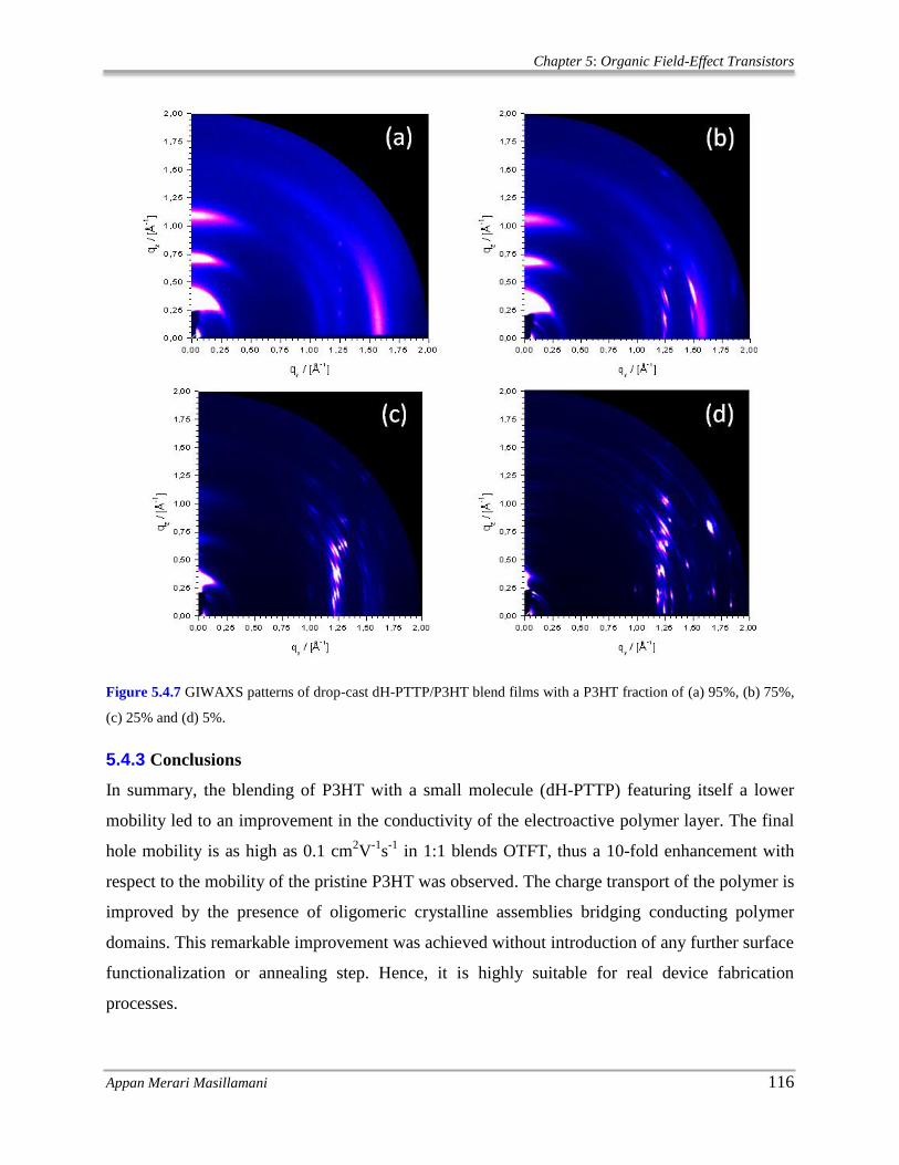
Chapter 5: Organic Field-Effect Transistors
Appan Merari Masillamani 116
Figure 5.4.7 GIWAXS patterns of drop-cast dH-PTTP/P3HT blend films with a P3HT fraction of (a) 95%, (b) 75%,
(c) 25% and (d) 5%.
5.4.3 Conclusions
In summary, the blending of P3HT with a small molecule (dH-PTTP) featuring itself a lower
mobility led to an improvement in the conductivity of the electroactive polymer layer. The final
hole mobility is as high as 0.1 cm2V
-1s
-1 in 1:1 blends OTFT, thus a 10-fold enhancement with
respect to the mobility of the pristine P3HT was observed. The charge transport of the polymer is
improved by the presence of oligomeric crystalline assemblies bridging conducting polymer
domains. This remarkable improvement was achieved without introduction of any further surface
functionalization or annealing step. Hence, it is highly suitable for real device fabrication
processes.

Chapter 5: Organic Field-Effect Transistors
Appan Merari Masillamani 117
5.4.4 References
1 Dimitrakopoulos, C. D. & Malenfant, P. R. L. Organic thin film transistors for large area
electronics. Adv. Mater. 14, 99 (2002).
2 Gelinck, G. H. et al. Flexible active-matrix displays and shift registers based on solution-
processed organic transistors. Nat. Mater. 3, 106, (2004).
3 Dodabalapur, A. Organic and polymer transistors for electronics. Mater. Today 9, 24 (2006).
4 Noh, Y. Y., Zhao, N., Caironi, M. & Sirringhaus, H. Downscaling of self-aligned, all-printed
polymer thin-film transistors. Nat. Nanotech. 2, 784, (2007).
5 Smits, E. C. P. et al. Bottom-up organic integrated circuits. Nature 455, 956, (2008).
6 Yan, H. et al. A high-mobility electron-transporting polymer for printed transistors. Nature 457,
679, (2009).
7 Arias, A. C., MacKenzie, J. D., McCulloch, I., Rivnay, J. & Salleo, A. Materials and Applications
for Large Area Electronics: Solution-Based Approaches. Chem Rev 110, 3, (2010).
8 Mas-Torrent, M. & Rovira, C. Novel small molecules for organic field-effect transistors: towards
processability and high performance. Chem Rev 37, 827, (2008).
9 Sirringhaus, H. et al. Two-dimensional charge transport in self-organized, high-mobility
conjugated polymers. Nature 401, 685 (1999).
10 Park, S. K., Jackson, T. N., Anthony, J. E. & Mourey, D. A. High mobility solution processed
6,13-bis(triisopropyl-silylethynyl) pentacene organic thin film transistors. Appl. Phys. Lett. 91,
063514, (2007).
11 Anthony, J. E. et al. Chromophore fluorination enhances crystallization and stability of soluble
anthradithiophene semiconductors. J. Am. Chem. Soc. 130, 2706, (2008).
12 Russell, D. M. et al. Blends of semiconductor polymer and small molecular crystals for
improved-performance thin-film transistors. Appl. Phys. Lett. 87, 222109, (2005).
13 Anthopoulos, T. D. et al. Solution-processed organic transistors based on semiconducting blends.
J. Mater. Chem. 20, 2562, (2010).
14 Hamilton, R. et al. High-Performance Polymer-Small Molecule Blend Organic Transistors. Adv.
Mater. 21, 1166, (2009).
15 Dabirian, R. et al. The Relationship between Nanoscale Architecture and Charge Transport in
Conjugated Nanocrystals Bridged by Multichromophoric Polymers. J. Am. Chem. Soc. 131, 7055,
(2009).
16 Liscio, A. et al. Charge transport in graphene-polythiophene blends as studied by Kelvin Probe
Force Microscopy and transistor characterization. J. Mater. Chem. 21, 2924, (2011).
17 Katz, H. E., Mushrush, M., Facchetti, A., Lefenfeld, M. & Marks, T. J. Easily processable
phenylene-thiophene-based organic field-effect transistors and solution-fabricated nonvolatile
transistor memory elements. J. Am. Chem. Soc. 125, 9414, (2003).
18 Vaidyanathan, S. et al. Investigation of solubility-field effect mobility orthogonality in substituted
phenylene-thiophene co-oligomers. Chem. Mater. 19, 4676, (2007).
19 Bonini, M. et al. Competitive Physisorption Among Alkyl-Substituted pi-Conjugated Oligomers
at the Solid-Liquid Interface: Towards Prediction of Self-Assembly at Surfaces from a
Multicomponent Solution. Small 5, 1521, (2009).
20 Smith, J. et al. The Influence of Film Morphology in High-Mobility Small-Molecule:Polymer
Blend Organic Transistors. Adv. Funct. Mater. 20, 2330, (2010).
21 Mushrush, M., Facchetti, A., Lefenfeld, M., Katz, H. E. & Marks, T. J. Easily Processable
Phenylene−Thiophene-Based Organic Field-Effect Transistors and Solution-Fabricated
Nonvolatile Transistor Memory Elements. J. Am. Chem. Soc. 125, 9414-9423, (2003).
22 Mannsfeld, S. C. B., Tang, M. L. & Bao, Z. Thin Film Structure of Triisopropylsilylethynyl-
Functionalized Pentacene and Tetraceno[2,3-b]thiophene from Grazing Incidence X-Ray
Diffraction. Adv. Mater. 23, 127-131, (2011).


Chapter 6: Charge Transport Through SAMs
Appan Merari Masillamani 119
There is nothing too difficult to be accomplished when done carefully with unflinching endeavor.
-Thiruvalluvar, Poet and Philosopher
6 Charge Transport
through SAMs
6.1 CHARGE INJECTION AND TRANSPORT THROUGH BIPHENYLTHIOL SAMS
This section describes the molecular structure-electronic function relationship for a series of
biphenylthiol derivatives with varying torsional degree of freedom in their molecular backbone
when self-assembled on gold electrodes. These biphenyl thiol molecules chemisorbed on Au
exhibit different tilt angles with respect to the surface normal and different packing densities.
The charge transport through the biphenyl thiol self-assembled monolayers (SAMs) showed a
characteristic decay trend with the effective monolayer thickness. Based on parallel pathways
model the tunneling decay factor β was estimated to be 0.27 Å-1
. The hole mobility of poly(3-
hexylthiophene)-based thin film transistors incorporating a biphenyl thiol SAM coating the Au
source and drain electrodes revealed a dependence on the injection barrier with the highest
occupied molecular orbital (HOMO) level of the semiconductor. The possible role of the
resistivity of the SAMs on transistor electrodes on the threshold voltage shift is discussed. The
control over the chemical structure, electronic properties and packing order of the SAMs
provides a versatile platform to regulate the charge injection in organic electronic devices.
6.1.1 Introduction
The prediction by Aviram and Ratner that organic molecules could exhibit the property of
electrical current rectification1 triggered remarkable research efforts which have been blooming
with the emergence of molecular electronics. The nanoscale electronic properties in molecule
based junctions can be controlled through a proper molecular design.2-4
A particular approach for
preparation of molecular junctions is the chemisorption of sulfur exposing molecules on metallic
surfaces like Au, Ag and Pt, which provides a facile route to form highly ordered self-assembled
monolayers (SAMs).5-7
These junctions can feature distinct functionalities including electrical
current rectification,4,8
photo responsive current switching,3,9-11
wettability and work function
modification.12,13
These tunable properties, which depend on the choice of the molecule and
metal electrode, have been shown to make SAMs ideal component for optimizing the charge

Chapter 6: Charge Transport Through SAMs
Appan Merari Masillamani 120
injection at metal-organic interfaces for application in organic thin-film transistors (OTFTs)12-15
A deep knowledge on the transport properties through the SAMs can thus be a determinant
information for the design and further fabrication of the organic electronic devices incorporating
these monolayers. The charge transport through molecules sandwiched between two metallic
electrodes has been probed using a variety of different techniques such as conducting-probe
atomic force microscopy (CP-AFM),3,16,17
Hg droplet based electrodes,18,19
mechanically
controlled break junctions,20-22
scanning tunneling microscopy (STM),2,23
nano-pores,24
crossed-
wire tunneling junctions,25
junctions formed via surface-diffusion-mediated deposition
(SDMD),26
and non-intrusive conformal junctions on the SAM comprising of a liquid metallic
gallium indium (GaInE) tip as the probe electrode.
27 Each of the above mentioned techniques has
its own pros and cons with variable range of set-up complexities, junction areas, geometry of
contacts and conditions necessary for experimentation. The GaInE based junction is particularly
interesting since it exploits the peculiar property of the eutectic alloy of the liquid metallic
gallium and indium to behave like a non-Newtonian liquid at room temperature. Importantly, it
can be molded into conical tip which retains its shape under ambient conditions. Significantly,
GaInE
features an intrinsic property to form a thin oxide layer (~ 1-2 nm) when exposed to air;
importantly, such a self-bounding oxide (Ga2O3) sheath enables the bulk of the underlying GaInE
to hold its shape.27
The ease of forming reliable and reproducible conical shaped GaInE tips has
been exploited to study the charge transport of delicate µcm2 sized single molecular layer
junctions.4,27-30
In contrast, other types of counter-electrodes like those based on Hg-drop needed a protecting
alkanethiol layer coating the counter-electrode to improve the yield31
by mitigating formation of
junction short-circuits when placing the drop in contact with the SAM on the metallic
substrate.19,32,33
Similarly, thin conducting film of PEDOT:PSS polymer11,34
or graphene35
has
been employed to protect the SAM prior to deposition of top Au electrodes in large area
molecular junctions.
Traditionally n-alkanethiols have been widely studied,16,19,23,24,30,34,36,37
and successfully
employed to change the wettability and work function properties of gold contacts, but their scope
as functional components for molecular electronic devices is limited. The better conducting
aromatic compounds offer a far more versatile platform to modulate their electronic properties

Chapter 6: Charge Transport Through SAMs
Appan Merari Masillamani 121
by altering the chemical structure of the molecule28,38-44
or by influence of external stimuli like
thermal energy or light.3,29,33
Here we have designed and synthesized a new library of mono-thiolated biphenyl molecules
featuring different torsion angles between the two phenyl subunits along the molecular
backbone. Although there have been studies on the single molecular conductance of biphenyl
units thiolated in both α and ω positions,2,45,46
the charge transport through biphenyl mono-thiol
SAMs with varying torsion in the molecular long axis have not yet been explored on a
macroscopic scale. On the one hand, once chemisorbed on Au(111), we investigated the charge
transport through the biphenyl mono-thiol SAMs embedded in a two terminal junction based on
a top GaInE counter-electrode. On the other hand, we functionalized the source and drain
electrodes of OTFTs with biphenyl mono-thiol SAMs exploited them to tune the charge injection
at the metal-organic interface of the devices.
The torsion angle between individual aromatic rings in doubly thiolated biphenyl derivatives has
been shown, via single molecule break junction based on STM, to govern the electrical
conductivity across single molecular scale.2,45,46
Both theoretical40
and experimental results2,45-47
provided evidence for a correlation between the cosine square of the torsions angle and the single
molecule conductance. The increasing torsion angle is accompanied by a decrease in the extent
of the geometrical overlap of pz orbitals; as a result the corresponding single molecular
conductance decreases since the electron transfer rates scale as a function of the square of pz
orbital overlap. Moreover if the contribution due to tunneling transport through the σ-orbitals is
neglected, the theory predicts a linear relationship between the molecular conductance with the
square of the cosine of torsion angle.48
The different mono-thiolated biphenyl derivatives exploited and characterized in the present
study are:
Molecule 1: 9H-fluorene-2-thiol, denoted here as 5m BPT due to the fluorene group bridging the
two individual phenyl rings;
Molecule 2: 1,2-bis(9,10-dihydrophenanthren-2-yl)disulfane denoted as 6m BPT;
Molecule 3: [1,1΄-biphenyl]-4-thiol denoted as BPT;

Chapter 6: Charge Transport Through SAMs
Appan Merari Masillamani 122
Molecule 4: 2,2΄-dimethyl-[1,1΄-biphenyl]-4-thiol denoted as tBPT (i.e., twisted BPT).
See ref for the complete synthesis details of the biphenylthiol derivatives.
6.1.2 SAM Packing Density and Orientation
6.1.2.1 HRXPS on biphenylthiol SAMs.
The C 1s and S 2p HRXPS spectra of all the SAMs used in this study are shown in Error!
Reference source not found.. The spectra were gathered at wave energies of 350 eV and 580 eV
for the C 1s and at 350 eV for the S 2p emission. In the C 1s spectra a single emission at 284.2-
284.3 eV is observed, which is attributed to the aromatic backbone of the SAM constituents.
Figure 6.1.1 C 1s (left and middle panels) and S 2p (right panel) HRXPS spectra of the target SAMs acquired at
photon energies of 350 eV (left and right panels) and 580 eV (middle panel). The red lines are guide for the eye and
are placed at a BE of 284.2eV.
A characteristic emission in a similar binding energy (BE) range of 284.2-284.3 eV has
previously been reported for biphenyl-derivative dithiols (BPDTs).49
The S 2p spectra of the
SAMs are dominated by the S 2p3/2,1/2 doublet with at 162.0 eV (S 2p3/2) corresponding to a
thiolate-type bonding of the SAM constituents to the substrate.49,50
This doublet is the only
feature in the spectra of 6m BPT and 5m BPT SAMs but is accompanied by an additional weak
doublet at a BE of ~161.0 eV (S 2p3/2) in the spectra of BPT and tBPT monolayers and by a
further weak doublet at a BE of 163.4-163.5 eV in the spectrum of tBPT SAMs. The former
doublet can be assigned to the differently (but strongly) bound SAM constituents while the latter

Chapter 6: Charge Transport Through SAMs
Appan Merari Masillamani 123
to the unbound or weakly bound molecules which are either caught in the hydrocarbon matrix of
the SAM or physisorbed at the SAM/ambience interface,51
the content of all these species is
however quite low.
Further, the effective thicknesses of the SAMs were calculated according to standard procedure
using the intensity ratios of the C 1s and the Au 4f signals and the standard attenuation lengths
for the Au 4f and C 1s emissions at the given kinetic energies.50,52
In addition to the above
thickness values, the packing density in the target SAMs were estimated on the basis of the
S2p/Au4f intensity ratio, using a SAM with a known packing density, viz. dodecanethiol on
Au(111) in the given case, as a reference.53
The derived values of the effective thickness and
packing density of the target SAMs are displayed in Table 6.1-1. A smaller thickness of the SAM
in comparison to the estimate of the length of the BPT molecule (~12 Å) in the gas phase
suggests that the SAM constituents have some degree of inclination. The packing density of the
target SAMs is of the following trend BPT > 6m BPT > 5m BPT > tBPT.
Table 6.1-1 Effective SAM thickness in Å along with packing density of the molecules in for the different BPT
SAMs in comparison to the reference of dodecanethiol SAM.
6.1.2.2 NEXAFS measurements.
Figure 6.1.2 shows the C K-edge NEXAFS spectra of the target SAMs. The spectra in the panel
were acquired at the so called magic X-ray incidence angle (55°), which offers spectra
independent of the molecular orientation, representative of the electronic structure of the only
unoccupied molecular orbitals.54
The curves in the right panel are the differences between the
spectra acquired at X-ray incidence angles of 90° and 20°; such curves are representative of the
molecular orientation.54
The spectra are dominated by the intense π1* resonance of the phenyl
rings at ~285.1 eV accompanied by the respective π2* resonance at 288.8 eV, the R*/C-S*

Chapter 6: Charge Transport Through SAMs
Appan Merari Masillamani 124
resonance at ~287.8 eV, and several broad σ* resonances at higher photon energies (the
assignments were performed in accordance with literature data).49,50,55-57
Note that the pattern of
the absorption resonances for the SAMs used in this study is similar to that of benzene as can be
expected.52,58
In the case of BPT SAM this pattern can be attributed to the localization of the
excited molecular orbitals at a particular aromatic ring.58
In accordance with the literature data,49
the aliphatic bridging group in the 5m and 6m BPT does not change this pattern significantly,
which means that the conjugation between the aromatic rings is not affected. Note that this
correlates with the spacing between the rings in these compounds which exceeds a critical value
of 1.477 Å.59
On the basis of the intensity of the 1* resonance, the quality of the target SAMs
follows the trend BPT > 5m BPT > 6m BPT > tBPT in agreement with the HRXPS results (see
previous Section). In addition, the 1* resonance for the tBPT SAMs is somewhat broader than
for the other monolayers of the given study, which is a further evidence for the higher degree of
heterogeneity in this particular film.
Figure 6.1.2 C K-edge NEXAFS spectra of the target SAMs acquired at an incidence angle of 55° (left panel) and
the difference of the spectra acquired at X-ray incidence angles of 90° and 20° (right panel). Horizontal dashed lines
in the right panel correspond to zero.
In addition to the above analysis of the 55° spectra, information on the molecular orientation in
the target SAMs could be obtained on the basis of the entire set of the NEXAFS data. In
particular, the average tilt angle of the aromatic chains in these films can be estimated by a

Chapter 6: Charge Transport Through SAMs
Appan Merari Masillamani 125
quantitative analysis of the angular dependence of the NEXAFS resonance intensities55
. For this
analysis, the 1* resonance was selected as the most intense and distinct resonance in the
absorption spectra. In addition, the intensities of this resonance could be derived directly from
the NEXAFS spectra, without a sometimes ambiguous fitting procedure. As soon as these
intensities I are known, the average tilt angle α of the 1* orbitals with respect to the surface
normal can be derived from a standard expression for a vector-type orbital,54
222 sin
2
1)1()1cos3()1cos3(
2
11
3
1),( PPAI
(6.1.1)
where A is a constant, α is the average tilt angle of the molecular orbital, P is the polarization
factor and θ is the incidence angle of the incoming X-rays. The tilt angle of the orbitals is
directly related to the tilt angle of the molecular axis with respect to the surface normal and to
the average twist angle of the aromatic rings with respect to the plane spanned by the surface
normal and the molecular axis.60
sincoscos (6.1.2)
This expression allows estimation of the tilt angle of the molecular axis as soon as some
assumptions about the value of the twist angle are made. In the case of the SAMs of this study it
is reasonable to assume a herringbone arrangement which is typical for aromatic bulk systems
and for aromatic SAMs.61,62
This means two different spatial orientations of the aromatic
moieties occurring with opposite signed (i.e., reverse) twist angles = 2 and the similar tilt
angles φ1 = φ2. The different signs of the twist angle are not a problem since cos is an
even function. The most reasonable assumption for the absolute value of the twist angle is 32°
which is the value observed in the biphenyl bulk materials61
and well applicable to aromatic
SAMs.60,63,64
Table 6.1-2 collects the estimated average tilt angle of π1* orbitals (α), tilt angles of
molecules (φ) and the assumed twist angle (). Note that we assume a coplanar arrangement of
individual rings within the biphenyl backbone in the BPT SAMs, which is a reasonable
assumption considering that this arrangement is typical for densely aromatic compounds where
the dihedral rotation is lifted due to the intermolecular interaction.61
The backbone of 5m BPT
SAMs has the planar conformation,65
while the torsion angle for the backbone of the 6m BPT
SAM is ~16.8° (see Table 6.1-3 and ref.66
). The torsion angle for the backbone of the tBPT SAM

Chapter 6: Charge Transport Through SAMs
Appan Merari Masillamani 126
is close to 80° (see Table 6.1-3 and ref.49
), so that the assumed twist angle can only be considered
as an average value over the both rings. The accuracy of the derived tilt angles is about ±3°
which is partly related to the uncertainty of the twist angles. The derived tilt angles represent
average values over macroscopic area of the SAM and thus can be taken as a fingerprint of the
orientational order. Indeed, a totally disordered molecular film exhibits no linear dichroism and
can be associated with an average tilt angle of a vector orbital of 54.7° since I(a,q) does not
depend on q at a = 54.7° (see eq 1). A deviation from this value, as it occurs for the SAMs of this
study, means a certain degree of the orientational order, with a higher degree for a higher
deviation.
The highest orientational order is observed for the BPT and 5m BPT SAMs, in accordance with
the planar conformation of 5m BPT65
and the assumed planar conformation of BPT;59,61
such a
conformation should favor high orientational order and dense molecular packing. Even slight
deviation from the planar conformation, as is the case for 6m BPT66
results in a lower packing
density (see previous section) and some deterioration of the orientational order (see Table 6.1-2).
Finally, a distinct non-planar conformation adopted by tBPT causes even lower packing density
(see previous Section) and even worse orientational order (see Table 6.1-2). Thus, the results from
the HRXPS and NEXAFS seem to corroborate the fact that the quality and packing density of the
SAMs is the highest for the BPT SAM, slightly worse for the 5m BPT SAMs, distinctly worse
for the 6m BPT SAMs, and the worst for the tBPT SAMs, in full correlation to the torsion angle
in the biphenyl backbone. The slightly better quality of the BPT SAMs as compared to the 5m
BPT monolayers is presumably related to the presence of the side bridge in the latter case, which
can be associated with additional sterical demands.
Table 6.1-2 Tilt angle and parameters estimated from the NEXAFS data.
a solid state torsion angle.
b average tilt angle of π1* molecular orbital.
c assumed twist angle.
d
average tilt angle all in degrees.

Chapter 6: Charge Transport Through SAMs
Appan Merari Masillamani 127
6.1.3 Charge Transport through Biphenylthiol SAMs
To gain insight into the charge transport across the target SAMs supported on Au we performed
I-V measurements in 2-terminal junctions by using a GaInE tip as the top counter-electrode. We
describe the junctions formed following the naming convention AuSAM/Ga2O3||GaInE in which
“–” indicates a covalently bonded contact, “/” denotes the physically formed contact between the
surface of the SAM and the Ga2O3 layer, and “||” denotes the interface between Ga2O3 and GaInE
bulk.
Tunneling is known to be the governing charge transport mechanism through π-conjugated
molecules shorter than ~3 nm.67,68
The current density (J) due to tunneling typically follows an
exponential decay with molecular length according to the simplified approximation of Simmons
model, J = J0 e-βd
where d is the molecular length (in Å) (in this present work d is considered to
be the SAM effective thickness) and β (in Å-1
) is the tunneling decay constant. To gather
adequate amount statistical data for the range of charge tunneling through the target SAMs we
formed a minimum of at least 20 junctions for each of these monolayers and analyzed the
resulting data without “selecting”, “eliminating”, “excluding” or “discarding” any of the
recorded data points to arrive at the actual range of J distribution across each of the SAMs. The
oxide skin covering the GaInE bulk was reported to have an electrical resistivity of 0.4 MΩcm,
corresponding to a J of 5.5 A/cm2 at 0.2 V,
69 which is much lower than the resistivity of any
SAM in this study. The above current density is nearly 3 orders of magnitude greater than the
analogous value for the tBPT SAM (J = 2.1 10-2
A/cm2 at 0.2 V) which is the most conductive
sample in this study. This would imply that the corresponding resistance of the least resistive
tBPT SAM is ~3 orders of magnitude greater than the Ga2O3 layer. Hence the resistivity
contribution of the oxide skin to the overall J measured for the junctions can be reasonably
neglected, since the total resistance is the direct sum of the two individual resistive components
of the oxide in series with that of the SAM. Figure 6.1.3 shows the variation of the mean of log|J|
with the applied bias across the junctions for all SAMs of this study. The charge transport
through these monolayers clearly shows a trend which would be expected in the case of non-
resonant tunneling.70,71
The distribution of J through the SAM follows a log-normal tendency
this is attributed to the exponential dependence of charge tunneling over the distance d.19,30,72
In
addition the J is more biased to higher values which arises due to junction shorts conversely the

Chapter 6: Charge Transport Through SAMs
Appan Merari Masillamani 128
log-mean of J (μlog|J|) results in a more reasonable estimate of J taking into account the high and
low end (i.e., shorts and non-contact J(V) traces respectively) of the distribution of J. The
geometric mean of log|J| is given by,
JJ
log10
log
In which
jnn
obs
obs
jn
J Jn 1
10|log| log1
(6.1.3)
Where njn is the total number of J observations (Jobs) recorded at a particular voltage taken from
the J-V traces.
Figure 6.1.3 Characteristics of mean log current density as a function of junction bias for the Au-5m
BPT/Ga2O3||GaInE, Au-6m BPT/Ga2O3||GaIn
E, Au-BPT/Ga2O3||GaIn
E and Au-tBPT/Ga2O3||GaIn
E junctions
indicating forward and reverse traces. The arrow indicates the bias value from which the log|J| values were extracted
to populate the histogram.
Figure 6.1.4 exhibits the log|J| distributions for the 5m BPT, 6m BPT, BPT and tBPT SAMs,
respectively. The log-normal histograms for each of the monolayers were populated by taking
the log|J| values at a bias voltage of 0.4V. From the peak of the Gaussian fitting of the
histograms it was possible to estimate the μlog|J| value which offers an estimate of highest
likelihood occurrence of J for a particular SAM. All histogram plotting and corresponding data
analysis were done using the ggplot273
package of R.74
Although in a chemisorbed SAM the
molecules are believed to be arranged in well-ordered (i.e., similar to a 2D crystal pattern)
-0.6 -0.4 -0.2 0.0 0.2 0.4 0.6
-7
-6
-5
-4
-3
-2
-1
5m BPT
6m BPT
BPT
tBPT
log
|J|
(Acm
-2)
Junction bias (V)
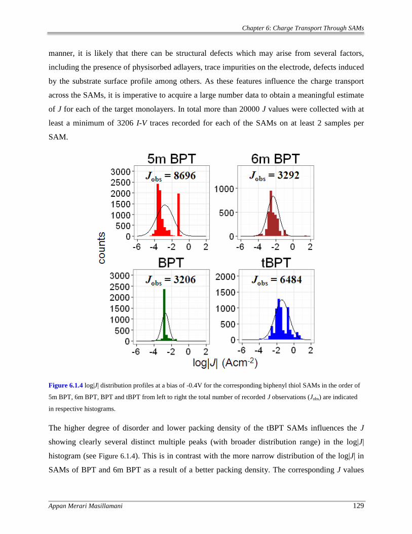
Chapter 6: Charge Transport Through SAMs
Appan Merari Masillamani 129
manner, it is likely that there can be structural defects which may arise from several factors,
including the presence of physisorbed adlayers, trace impurities on the electrode, defects induced
by the substrate surface profile among others. As these features influence the charge transport
across the SAMs, it is imperative to acquire a large number data to obtain a meaningful estimate
of J for each of the target monolayers. In total more than 20000 J values were collected with at
least a minimum of 3206 I-V traces recorded for each of the SAMs on at least 2 samples per
SAM.
Figure 6.1.4 log|J| distribution profiles at a bias of -0.4V for the corresponding biphenyl thiol SAMs in the order of
5m BPT, 6m BPT, BPT and tBPT from left to right the total number of recorded J observations (Jobs) are indicated
in respective histograms.
The higher degree of disorder and lower packing density of the tBPT SAMs influences the J
showing clearly several distinct multiple peaks (with broader distribution range) in the log|J|
histogram (see Figure 6.1.4). This is in contrast with the more narrow distribution of the log|J| in
SAMs of BPT and 6m BPT as a result of a better packing density. The corresponding J values

Chapter 6: Charge Transport Through SAMs
Appan Merari Masillamani 130
were used to populate the histograms. The statistical data for the recorded J values are collected
in Table 6.1-3 along with the molecular chemical structure.
The thickness of the SAMs depends on the tilt angle with respect to the surface normal, i.e. the
greater the tilt angle the lower the effective thickness that corresponds to the separation between
electrodes. An illustration of how the effective thickness of the SAM changes with increase of
the tilt angle is shown in . From the plot of log|J| vs. d (i.e., effective monolayer thickness) the
parameters J0 and β can be extracted on the basis of the y-intercept and linear slope, respectively.
We observed that the SAM with a greater tilt angle, i.e. tBPT-SAM, was more conductive than
that with a lower tilt angle, i.e. 5m BPT-SAM;, by a factor of ~27 in the linear scale (~2 in log|J|
magnitude). In oligo-aromatic architectures the charge tunneling contributions are likely due to
through-bond tunneling and through-space tunneling.75
Table 6.1-3 Molecular structure and charge transport properties of biphenyl thiol SAMs
a Molecular structure of different BPT derivatives used.
b Torsion angle between the planes of the phenyl rings from
x-ray structure adapted from ref 45 and 46. c Number of junctions formed.
d Total number of J observations for each
SAM. e Number of J-V traces which resulted in a short where I reach 10
-3 A. f
yield given as the ratio between the
difference between total and shorting J(V) traces to the total J observations. g Mean of log|J| from the log-normal
distribution of J. h Mean value of J.
Owing to the minimal difference in the molecular length for the biphenyl thiol derivatives it was
not possible to resolve unequivocally the influence of tunneling due to through-bond molecular
length.

Chapter 6: Charge Transport Through SAMs
Appan Merari Masillamani 131
Figure 6.1.5 Schematic illustration of the change in the effective SAM thickness with increase in the tilt angle of the
molecules with respect to the surface normal. The dark yellow circles and the green bars represent the sulfur atoms
and the molecular backbone respectively. The ratio of the width-to-height sufficiently represents the scaled-up
geometry of the biphenylthiol molecules on the gold surface.
To understand if the current density exhibits dependence on the SAM medium we plotted the
log|J| with respect to the effective monolayer thickness (Figure 6.1.6). We observed a β of 0.27 ±
0.08 Å-1
from data extracted at a bias of -0.4V (Figure 6.1.6); this is in agreement with the β
extracted from a series of phenylene oligomers based SAM measured in a large-area molecular
junction.71
Figure 6.1.6 Plot of log|J| vs. effective monolayer thickness for BPT SAMs at a bias of -0.4V showing the
respective tunneling decay factor estimated from the slope.
On closer inspection of the decay of current density with respect to the effective thickness for the
biphenyl thiol monolayers, it is clear that there is characteristic attenuation with increase in the
distance of separation. It is interesting to note that the log|J| dependence with cosine square
torsion angle for our biphenyl thiol SAMs exhibits an opposite trend observed in similar
molecules on a single molecular scale (see Figure 6.1.7).45,46

Chapter 6: Charge Transport Through SAMs
Appan Merari Masillamani 132
Figure 6.1.7 log|J| variation with the cosine square of torsion angle recorded at a bias of -0.4V.
We attribute this to the likely weaker cohesive interaction between the SAM and top GaInE
electrode8
which is considered to be of van der Waals nature, being in contrast to the much
stronger covalent electronic coupling between the biphenyl dithiol molecules and gold electrodes
studied by Vonlanthen et al.45,46
6.1.4 Biphenylthiol SAMs in OTFT electrodes
6.1.4.1 OTFT performance
To bestow information onto the charge injection properties of OTFT electrodes modified with
biphenyl-based SAMs we fabricated and characterized transistors in bottom-gate bottom-contact
device geometry by using P3HT as active semiconducting layer. The channel length (L) and
width (W) for the OTFTs under study amounted to 10 and 10000 µm, respectively. Given that
the performance of OTFTs was acutely sensitive enough to detect the subtle differences in
charge transport across SAMs chemisorbed on the source and drain electrodes,12
we sought to
determine the influence of the varying torsion angle molecules composing the SAM. Figure 6.1.8
shows the OTFT device configuration along with the chemical structure of the molecules
incorporated in the electrodes and the active layer of the transistor.
The route to modify the electrode work function (ΦM) by means of SAMs and thereby to adjust
the energy levels in the system to either inject or extract charge carriers (electrons or holes) more
effectively in organic electronic devices have been vastly exploited.14,76-80
In particular, the
chemisorption of alkanethiols and partially perfluoroalkanethiols has been used to lower or raise
the work function of Au electrodes, respectively, to ultimately improve the injection of electron

Chapter 6: Charge Transport Through SAMs
Appan Merari Masillamani 133
or holes.76
The shift in the work function is generally attributed to the total of effective dipole
moment formed between the Au-S bond along with the dipole moment due to monolayer
chemical composition of the molecule in the SAM,81
the tail groups contributing notably to the
overall interfacial dipole.82,83
Among different possibilities, the work function of the metal can
be measured by means of the contact potential difference (CPD) technique of a macroscopic
Kelvin probe. We extracted the work function of Au electrodes comprising of biphenyl-based
SAMs from the CPD using an Au reference tip (Φ ~ 5.1 eV). Table 6.1-4 collects the respective
data along with the work function of a bare Au electrode. The work function for the BPT SAM
was measured to be ~ 4.81 ± 0.01 eV, which is in the range of the reported value in literature.14
Figure 6.1.8 Schematic of the OTFT with the chemical structure of the molecules used in the SAM and the active
layer. The biasing configurations for the respective electrodes are indicated.
The work function difference between the more disordered Au-tBPT SAM with respect to the
ordered Au-BPT SAM was ~210 meV, note that being the molecules intrinsically quite non-
polar the effective shift in the work function due to the variability in packing densities and tilt
angle of the assembled monolayer is fairly evident from the recorded values of ΦM. The surface
wetting properties of the Au-SAM were estimated over macroscopic areas from the static water

Chapter 6: Charge Transport Through SAMs
Appan Merari Masillamani 134
contact angle (θca) measurements giving values spanning between ~70 and 79 degrees (see Table
6.1-4), therefore highlighting a higher hydrophobic nature of the coated electrodes respect to the
bare gold. The θca for Au-BPT SAM (~78.9º) was in excellent agreement for the similar type of
metal-SAM surface reported by us earlier.14
Note that these values match closely to the contact
angle reported in the literature for non-substituted biphenyl thiol SAMs on Au(111).84
The output
(drain current (ID) vs. source-drain voltage (VDS)) and transfer (ID vs. gate voltage (VGS))
characteristics were measured for the devices incorporating electrodes modified with the BPT
family SAMs and compared with devices with non-functionalized electrodes. The ID vs. VDS plot
obtained for the device with the biphenylthiol SAM (BPT SAM) modified electrodes are
portrayed in Figure 6.1.9.
Figure 6.1.9 Output characteristics for TFT based on Au-BPT SAM modified electrodes (W=10000 µm and L=
10µm) with respective VGS denoted.
The recorded ID vs. VGS curves for the TFTs with the electrodes modified with the different
SAMs are shown in Figure 6.1.10. The other key device performance indicators like turn on
voltage (Von) and the threshold voltage (VT) were estimated from the transfer plots. The Von is the
voltage value in which a change in slope sign occurs in the log scale on the transfer curves and
was extracted from the ID-VGS plots in the linear regime. VT is the intercept with gate voltage axis
from the plot of DI vs. VGS (Figure 6.1.10) and provides the value of gate potential at which
most of the traps levels are filled up.

Chapter 6: Charge Transport Through SAMs
Appan Merari Masillamani 135
Figure 6.1.10 Transfer curves for the OTFTs based on electrodes with different BPT SAMs showing variation of
square root of ID vs. VGS (left axis) and semilog ID vs. VGS (right axis) when VDS = -60 V with lines indicating 5m
BPT (red), 6m BPT (brown), BPT (green), tBPT (blue) and bare Au (black).
The hole injection barrier (Φbh+) is defined as the energy difference between IE and the WF of
the functionalized Au electrode. Note that the IE for the P3HT film used in our devices is ~ 4.86
± 0.02 eV as measured by ambient photoelectron spectroscopy (see Figure 6.1.14). The evaluated
injection barrier can give a good indication of the energetic mismatch at the metal-
SAM/semiconductor interface. The field-effect mobility was extracted from the saturation
regime by estimating the slope of the DI vs. VGS and then using the following relation
2
2
DSV
GS
D
i
sat
V
I
WC
L (6.1.4)
where Ci is the capacitance of the gate dielectric layer (230 nm of SiO2) and has a value of
15nF/cm2. For the P3HT solution, we used toluene which has a high boiling point (110.6°C)
since it was reported that higher boiling point solvents tend to promote formation of polymeric
micro crystalline domains in the active layer of the channel, which can enhance charge
transport.85
The devices incorporating the BPT SAM exhibited the highest field-effect mobility
with µh+ of 9.0×10⁻³
cm2/Vs. This result can be attributed to the combination of low energetic
injection barrier and better electrode wettability by the non-polar P3HT (P3HT film has a θca of
~106° on the surface of SiO2)86
over the other, more hydrophobic BPT-based monolayer (see

Chapter 6: Charge Transport Through SAMs
Appan Merari Masillamani 136
Table 6.1-4). The interfacial packing of the P3HT is likely to be better in more hydrophobic
electrodes. In contrast, the devices with Au-tBPT electrodes exhibited the lowest field-effect
mobility (µh+ of 6.4×10⁻³
cm2/Vs) in comparison with all other SAMs. This lower mobility for
devices comprising of Au-tBPT can be correlated with the relatively larger hole injection barrier
of 164 meV which is greater by a factor of ~4 than the devices with highest mobility injection
barrier for Au-BPT electrodes. The carrier mobility in organic semiconductors has been shown to
be influenced by the injection barrier with the charge injecting electrode.53
Hence the lower the
injection barrier the higher is the current injection efficiency. It has been shown for OTFTs the
contact resistance plays a big role in the lower source-drain bias87,88
while at sufficiently high
source-drain potentials the resistance offered by the contacts is limited.88
Since we estimate the
field-effect hole mobility at a VDS of -60 V, the effect of the contact resistance has been
reasonably omitted. Note that the standard deviation of mobility was within 15% indicating good
consistency for all the tested devices.
Table 6.1-4 Contact angle, work function of electrodes and other key device performance indicators
a Hole injection barrier with respect to the IE level of P3HT.
b Average hole mobility calculated in the saturation
regime along with the standard deviation for at least 8 devices. The surface of the clean bare Au is hydrophilic,89
the
θca of which was measured within 60 s after performing UV/Ozone treatment.
6.1.4.2 Morphology of Semiconductor
The morphology of the spin coated P3HT films (~ 8 nm thick measured with a profilometer) on
the modified Au electrodes of the OTFTs exhibited a fairly isotropic grain like morphology
featuring a lower roughness (Figure 6.1.11 a-d). Table 6.1-5 collects the root mean square
roughness (RRMS) for the Au-BPT SAMs/P3HT films.
electrode
surface
θ ca ± σ
(deg)
Ф M ± σ
(eV)
Φbh+
(meV)a
µ h+,sat ± σ x 10-3
(cm2/Vs)
b
V on ± σ
(V)
V T ± σ
(V)
bare Au 18.56 ± 4.20 4.88 ± 0.06 25 7.8 ± 1.0 8.8 ± 1.1 3.6 ± 0.6
5m BPT 71.63 ± 3.40 4.98 ± 0.01 121 6.7 ± 0.8 3.0 ± 5.4 -9.2 ± 5.5
6m BPT 69.30 ± 0.56 4.93 ± 0.01 72 7.2 ± 0.6 11.5 ± 1.4 0.3 ± 1.3
BPT 78.93 ± 1.88 4.81 ± 0.01 43 9.0 ± 0.6 5.5 ± 0.9 -8.4 ± 1.0
tBPT 67.96 ± 2.19 5.02 ± 0.02 164 6.4 ± 1.0 11.8 ± 1.9 2.2 ± 1.0

Chapter 6: Charge Transport Through SAMs
Appan Merari Masillamani 137
Table 6.1-5 Root mean square roughness (RRMS) for the Au-SAM and Au(111) electrode used in charge transport
measurements.
For the biphenyl SAMs on Au the lateral size is 2.0 x 2.0 µm2 and for the surface of Au(111) 5.0
x 5.0 µm2
Figure 6.1.11 Surface morphology of P3HT film on top of (a) Au-5m BPT SAM. (b) Au-6m BPT SAM. (c) Au-
BPT SAM. (d) Au-tBPT SAMs. Z scales are 7.6 nm
6.1.4.3 Morphology of Electrodes
To gain insight into the morphology of the gold OTFT source-drain electrodes and gold used for
charge transport measurements through SAMs we recorded topographic images by means of
tapping mode-AFM.
Surface RRMS (nm)
Au-5m BPT/P3HT 0.5441
Au-6m BPT/P3HT 0.5179
Au-BPT/P3HT 0.5438
Au-tBPT/P3HT 0.5412
Au(111) 1.2365
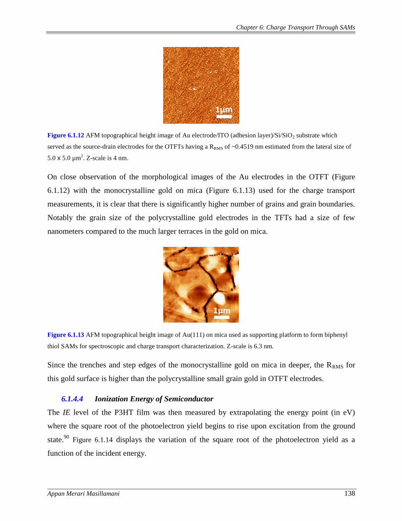
Chapter 6: Charge Transport Through SAMs
Appan Merari Masillamani 138
Figure 6.1.12 AFM topographical height image of Au electrode/ITO (adhesion layer)/Si/SiO2 substrate which
served as the source-drain electrodes for the OTFTs having a RRMS of ~0.4519 nm estimated from the lateral size of
5.0 x 5.0 µm2. Z-scale is 4 nm.
On close observation of the morphological images of the Au electrodes in the OTFT (Figure
6.1.12) with the monocrystalline gold on mica (Figure 6.1.13) used for the charge transport
measurements, it is clear that there is significantly higher number of grains and grain boundaries.
Notably the grain size of the polycrystalline gold electrodes in the TFTs had a size of few
nanometers compared to the much larger terraces in the gold on mica.
Figure 6.1.13 AFM topographical height image of Au(111) on mica used as supporting platform to form biphenyl
thiol SAMs for spectroscopic and charge transport characterization. Z-scale is 6.3 nm.
Since the trenches and step edges of the monocrystalline gold on mica in deeper, the RRMS for
this gold surface is higher than the polycrystalline small grain gold in OTFT electrodes.
6.1.4.4 Ionization Energy of Semiconductor
The IE level of the P3HT film was then measured by extrapolating the energy point (in eV)
where the square root of the photoelectron yield begins to rise upon excitation from the ground
state.90
Figure 6.1.14 displays the variation of the square root of the photoelectron yield as a
function of the incident energy.

Chapter 6: Charge Transport Through SAMs
Appan Merari Masillamani 139
Figure 6.1.14 The ionization energy was estimated to be 4.8 eV from the x-axis intercept of the photoelectron yield.
6.1.5 Discussions
In order to address the charge transport through the SAMs, the molecular structure, monolayer
structural defects and packing density are among the pertinent factors that should be considered.
The HRXPS data showed that the well-ordered BPT SAM on Au had a packing density ~1.5
greater than the tBPT monolayer which features the lowest orientational order. The molecular
packing densities are probably heavily influenced by the intramolecular steric hindrance in tBPT
SAM which indeed features the highest torsion angle. Closer inspection of the histograms
obtained from the charge transport measurements revealed a narrower log|J| distribution for well-
ordered BPT, 6m and 5m BPT SAMs if compared to the wider distribution for disordered tBPT
SAM. This suggests that the measured J are sensitive to the structural characteristics of the
biphenyl SAMs chemisorbed on Au. We believe that the charge transport through our biphenyl
thiol SAMs is due to a combination of pathways tunneling through the molecule along with
transport through inter chain hops between adjacent molecules. While the length of the pathway
through the molecular chain is the length of the molecule in its long axis, in the case of the
parallel pathways model proposed by Slowinski et al.75
the pathway due to the through space
hops decreases with the effective thickness of the SAM. Least square fitting of the current
density with the effective monolayer thickness yielded β of 0.27 ± 0.08 Å-1
.
The electrical resistivity (ρ) of the biphenyl thiol SAMs can be estimated from the current
density (estimated from the charge transport measurements with GaInE probe) dependence with
the applied electric field (E). As expected the ρ shows a monotonic increase with increasing

Chapter 6: Charge Transport Through SAMs
Appan Merari Masillamani 140
effective thickness (Figure 6.1.15). Note that despite the polycrystalline nature of the Au
electrodes in the OTFT and the monocrystalline character of the Au used for the measurements
with a GaInE-based junction (see section 6.1.4.3 for AFM images), a fairly good correlation
between the electrical resistivity and the relative threshold voltage shift for the transistor
comprising of biphenyl thiol coated electrodes was found.
Figure 6.1.15 Electrical resistivity dependence on effective thickness of the biphenyl thiol SAMs estimated for a
bias of -0.4V with a linear least squares fitting.
The VT extracted from the transfer curve in Fig. 6 was under biasing conditions where VGS was
swept from +20 V → -60 V while holding VDS fixed at -60 V. It was observed that the VT was ~
+2.2 V for transistors comprising Au-tBPT SAM electrodes and the corresponding electrical
resistivity ρ ~ 0.12 GΩcm also being the lowest; on the other hand the devices with Au-5m BPT
electrodes had a more negative shift of VT of -9.2 V and the highest ρ ~ 2.2 GΩcm (see Figure
6.1.15). This difference in the VT for devices based on Au-5m BPT electrodes of nearly 18 V in
the upper bounds when compared Au-tBPT can be attributed directly to the resistivity increase
by a similar one to one correlation (i.e., the ρ increases by factor of ~18 for electrodes
comprising of 5m BPT with respect to tBPT SAMs). For P3HT transistors the majority charge
carrier are holes (i.e., increase in ID tends to predominantly occur when VGS is negative). Note
that while the potential sweep for the gate electrode starts from positive voltage and proceeds to
the negative (Figure 6.1.10) the TFTs exhibited VT shifts towards more negative voltages in the
order of tBPT, 6m BPT, BPT and 5m BPT, being in good agreement with the concomitant trend
of increasing resistivity through the biphenyl thiol SAMs.
8 9 10 11 12
0.0
0.5
1.0
1.5
2.0
2.5
Resistivity (ohm cm)
% (3,@LG)
(
G
cm
)
effective thickness (Å)
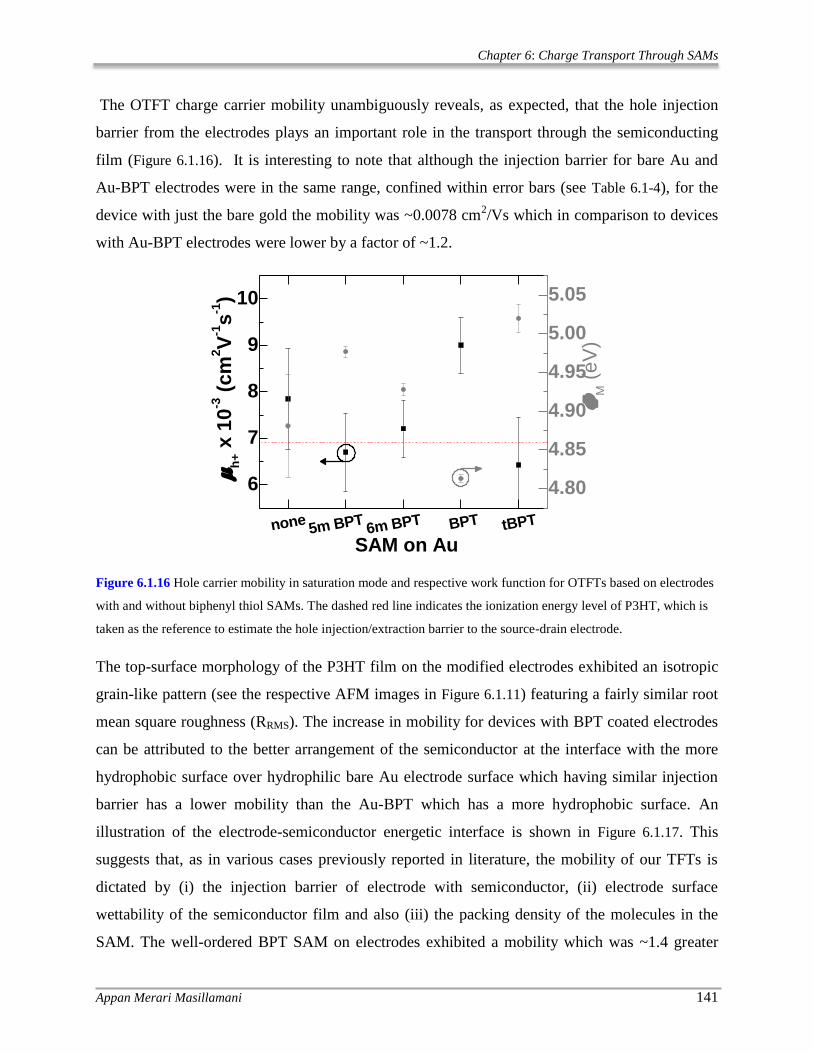
Chapter 6: Charge Transport Through SAMs
Appan Merari Masillamani 141
The OTFT charge carrier mobility unambiguously reveals, as expected, that the hole injection
barrier from the electrodes plays an important role in the transport through the semiconducting
film (Figure 6.1.16). It is interesting to note that although the injection barrier for bare Au and
Au-BPT electrodes were in the same range, confined within error bars (see Table 6.1-4), for the
device with just the bare gold the mobility was ~0.0078 cm2/Vs which in comparison to devices
with Au-BPT electrodes were lower by a factor of ~1.2.
Figure 6.1.16 Hole carrier mobility in saturation mode and respective work function for OTFTs based on electrodes
with and without biphenyl thiol SAMs. The dashed red line indicates the ionization energy level of P3HT, which is
taken as the reference to estimate the hole injection/extraction barrier to the source-drain electrode.
The top-surface morphology of the P3HT film on the modified electrodes exhibited an isotropic
grain-like pattern (see the respective AFM images in Figure 6.1.11) featuring a fairly similar root
mean square roughness (RRMS). The increase in mobility for devices with BPT coated electrodes
can be attributed to the better arrangement of the semiconductor at the interface with the more
hydrophobic surface over hydrophilic bare Au electrode surface which having similar injection
barrier has a lower mobility than the Au-BPT which has a more hydrophobic surface. An
illustration of the electrode-semiconductor energetic interface is shown in Figure 6.1.17. This
suggests that, as in various cases previously reported in literature, the mobility of our TFTs is
dictated by (i) the injection barrier of electrode with semiconductor, (ii) electrode surface
wettability of the semiconductor film and also (iii) the packing density of the molecules in the
SAM. The well-ordered BPT SAM on electrodes exhibited a mobility which was ~1.4 greater
none5m BPT
6m BPT BPT tBPT
6
7
8
9
10
SAM on Au
h
+ x
10
-3 (
cm
2V
-1s
-1)
4.80
4.85
4.90
4.95
5.00
5.05
M (
eV
)

Chapter 6: Charge Transport Through SAMs
Appan Merari Masillamani 142
than that of the mobility for devices based on more disordered Au-tBPT SAM, indeed reflecting
the variable packing density of the molecules adsorbed on the Au electrodes.
Figure 6.1.17 Schematic of the energetic mismatch between the Fermi level of the electrodes and the ionization
energy level of P3HT. The curved dashed lines gives an indication of the hole carrier injection barrier from the
electrode to the semiconductor.
Overall, the transistor responses show that our devices are an effective means to monitor the
energy level adjustment and the corresponding electronic coupling at the interface and the
threshold voltage shifts scale with the tunneling resistivity through the biphenyl SAMs on the Au
electrodes.

Chapter 6: Charge Transport Through SAMs
Appan Merari Masillamani 143
6.1.6 Conclusions
In summary, the charge transport through a family of biphenyl-based SAMs with varying torsion
angle chemisorbed on Au surfaces exhibits a good degree of correlation with the packing density
and orientational order in the monolayers. The latter parameters were mostly governed by
molecular conformation which was specifically adjusted by the site bridging or substitution of/at
the individual rings. The efficiency of the charge tunneling through the SAMs shows a
characteristic decay with the increasing separation between the metallic contacts (i.e, increase of
the effective SAM thickness). The charge transport experiments revealed a through-space β of
0.27 ± 0.08 Å-1
. For transistors the threshold voltage shifts were influenced by scaling resistivity
through biphenyl SAMs on electrodes. A good agreement between the transistor electrode-SAM
energetic injection barrier dependence on the field-effect mobility was found. These results show
that a proper design of thiolated molecules chemisorbed on Au electrodes is needed for realizing
more efficient organic electronic devices via improved control over the electrode-semiconductor
interface.

Chapter 6: Charge Transport Through SAMs
Appan Merari Masillamani 144
6.1.7 References
1 Aviram, A. & Ratner, M. A. Molecular rectifiers. Chem. Phys. Lett. 29, 277-283, (1974).
2 Venkataraman, L., Klare, J. E., Nuckolls, C., Hybertsen, M. S. & Steigerwald, M. L. Dependence
of single-molecule junction conductance on molecular conformation. Nature 442, 904-907,
(2006).
3 Mativetsky, J. M. et al. Azobenzenes as Light-Controlled Molecular Electronic Switches in
Nanoscale Metal−Molecule−Metal Junctions. J Am Chem Soc 130, 9192-9193, (2008).
4 Nijhuis, C. A., Reus, W. F., Siegel, A. C. & Whitesides, G. M. A Molecular Half-Wave Rectifier.
J Am Chem Soc 133, 15397-15411, (2011).
5 Bain, C. D. & Whitesides, G. M. Molecular-level control over surface order in self-assembled
monolayer films of thiols on gold. Science 240, 62 (1988).
6 Caldwell, W. B. et al. A Highly Ordered Self-Assembled Monolayer Film of an
Azobenzenealkanethiol on Au(111): Electrochemical Properties and Structural Characterization
by Synchrotron in-Plane X-ray Diffraction, Atomic Force Microscopy, and Surface-Enhanced
Raman Spectroscopy. J Am Chem Soc 117, 6071-6082, (1995).
7 Pace, G. et al. Cooperative light-induced molecular movements of highly ordered azobenzene
self-assembled monolayers. P Natl Acad Sci USA 104, 9937-9942, (2007).
8 Nijhuis, C. A., Reus, W. F. & Whitesides, G. M. Molecular Rectification in Metal-SAM-Metal
Oxide-Metal Junctions. J Am Chem Soc 131, 17814-17827, (2009).
9 Crivillers, N., Orgiu, E., Reinders, F., Mayor, M. & Samorì, P. Optical Modulation of the Charge
Injection in an Organic Field-Effect Transistor Based on Photochromic Self-Assembled-
Monolayer-Functionalized Electrodes. Adv Mater 23, 1447-1452, (2011).
10 Karpe, S. et al. Oligothiophene-derivatized azobenzene as immobilized photoswitchable
conjugated systems. Chem Commun 46, 3657-3659, (2010).
11 Kronemeijer, A. J. et al. Reversible Conductance Switching in Molecular Devices. Adv Mater 20,
1467-1473, (2008).
12 Stoliar, P. et al. Charge injection across self-assembly monolayers in organic field-effect
transistors: Odd-even effects. J Am Chem Soc 129, 6477-6484 (2007).
13 Cheng, X. et al. Controlling Electron and Hole Charge Injection in Ambipolar Organic Field‐Effect Transistors by Self‐Assembled Monolayers. Adv Funct Mater 19, 2407-2415 (2009).
14 Orgiu, E., Crivillers, N., Rotzler, J., Mayor, M. & Samori, P. Tuning the charge injection of
P3HT-based organic thin-film transistors through electrode functionalization with oligophenylene
SAMs. J. Mater. Chem. 20, 10798 (2010).
15 Gemayel, M. E. et al. Tuning the Photoresponse in Organic Field-Effect Transistors. J Am Chem
Soc 134, 2429-2433, (2012).
16 Engelkes, V. B., Beebe, J. M. & Frisbie, C. D. Length-Dependent Transport in Molecular
Junctions Based on SAMs of Alkanethiols and Alkanedithiols: Effect of Metal Work Function
and Applied Bias on Tunneling Efficiency and Contact Resistance. J Am Chem Soc 126, 14287-
14296, (2004).
17 Engelkes, V. B., Beebe, J. M. & Frisbie, C. D. Analysis of the Causes of Variance in Resistance
Measurements on Metal−Molecule−Metal Junctions Formed by Conducting-Probe Atomic Force
Microscopy. J. Phys. Chem. B 109, 16801-16810, (2005).
18 Selzer, Y., Salomon, A. & Cahen, D. The Importance of Chemical Bonding to the Contact for
Tunneling through Alkyl Chains. J. Phys. Chem. B 106, 10432-10439, (2002).
19 Weiss, E. A. et al. Influence of Defects on the Electrical Characteristics of Mercury-Drop
Junctions: Self-Assembled Monolayers of n-Alkanethiolates on Rough and Smooth Silver. J Am
Chem Soc 129, 4336-4349, (2007).
20 Gonzalez, M. T. et al. Nano Lett 6, 2238-2242 (2006).
21 Reed, M. A., Zhou, C., Muller, C. J., Burgin, T. P. & Tour, J. M. Science 278, 252-254 (1997).
22 Reichert, J. et al. Phys. Rev. Lett. 88, 1768041-1768044 (2002).

Chapter 6: Charge Transport Through SAMs
Appan Merari Masillamani 145
23 Cui, X. D. et al. Reproducible Measurement of Single-Molecule Conductivity. Science 294, 571-
574, (2001).
24 Wang, W., Lee, T. & Reed, M. A. Mechanism of electron conduction in self-assembled
alkanethiol monolayer devices. Phys Rev B 68, 035416 (2003).
25 Kushmerick, J. G. et al. Metal-Molecule Contacts and Charge Transport across Monomolecular
Layers: Measurement and Theory. Phys. Rev. Lett. 89, 086802 (2002).
26 Bonifas, A. P. & McCreery, R. L. /Soft/'Au, Pt and Cu contacts for molecular junctions through
surface-diffusion-mediated deposition. Nature Nanotech. 5, 612-617 (2010).
27 Chiechi, R. C., Weiss, E. A., Dickey, M. D. & Whitesides, G. M. Eutectic Gallium–Indium
(EGaIn): A Moldable Liquid Metal for Electrical Characterization of Self-Assembled
Monolayers. Angew Chem 120, 148-150, (2008).
28 Fracasso, D., Valkenier, H., Hummelen, J. C., Solomon, G. C. & Chiechi, R. C. Evidence for
Quantum Interference in SAMs of Arylethynylene Thiolates in Tunneling Junctions with Eutectic
Ga–In (EGaIn) Top-Contacts. J Am Chem Soc 133, 9556-9563, (2011).
29 Lilly, G. D. et al. Switchable photoconductivity of quantum dot films using cross-linking ligands
with light-sensitive structures. J. Mater. Chem. 21 (2011).
30 Thuo, M. M. et al. Odd-Even Effects in Charge Transport across Self-Assembled Monolayers. J
Am Chem Soc 133, 2962-2975, (2011).
31 Yield is referred to as ratio of the difference between the total number of J(V) traces to the traces
that ended up with a short (instrument reached compliance limit) with the total J observations.
32 Tran, E. et al. Experimental approaches for controlling current flowing through metal–molecule–
metal junctions. Adv Mater 18, 1323-1328 (2006).
33 Ferri, V. et al. Light-powered electrical switch based on cargo-lifting azobenzene monolayers.
Angew Chem Int Edit 47, 3407-3409, (2008).
34 Akkerman, H. B., Blom, P. W. M., de Leeuw, D. M. & de Boer, B. Towards molecular
electronics with large-area molecular junctions. Nature 441, 69-72, (2006).
35 Wang, G., Kim, Y., Choe, M., Kim, T.-W. & Lee, T. A New Approach for Molecular Electronic
Junctions with a Multilayer Graphene Electrode. Adv Mater 23, 755-760, (2011).
36 Love, J. C., Estroff, L. A., Kriebel, J. K., Nuzzo, R. G. & Whitesides, G. M. Self-Assembled
Monolayers of Thiolates on Metals as a Form of Nanotechnology. Chem. Rev. 105, 1103-1170,
(2005).
37 Qi, Y. et al. Mechanical and Charge Transport Properties of Alkanethiol Self-Assembled
Monolayers on a Au(111) Surface: The Role of Molecular Tilt. Langmuir 24, 2219-2223, (2008).
38 Li, D., Swanson, B. I., Robinson, J. M. & Hoffbauer, M. A. Porphyrin based self-assembled
monolayer thin films: synthesis and characterization. J Am Chem Soc 115, 6975-6980, (1993).
39 Anariba, F., Steach, J. K. & McCreery, R. L. Strong Effects of Molecular Structure on Electron
Transport in Carbon/Molecule/Copper Electronic Junctions. J. Phys. Chem. B 109, 11163-11172,
(2005).
40 Wolfgang, H. et al. Variable contact gap single-molecule conductance determination for a series
of conjugated molecular bridges. J. Phys. Condens. Matter 20, 374119 (2008).
41 Ricks, A. B. et al. Controlling Electron Transfer in Donor−Bridge−Acceptor Molecules Using
Cross-Conjugated Bridges. J Am Chem Soc 132, 15427-15434, (2010).
42 Bruno, G. et al. Tailoring Density and Optical and Thermal Behavior of Gold Surfaces and
Nanoparticles Exploiting Aromatic Dithiols. Langmuir 26, 8430-8440, (2010).
43 Operamolla, A., Omar, O. H., Babudri, F., Farinola, G. M. & Naso, F. Synthesis of S-acetyl
oligoarylenedithiols via Suzuki-Miyaura cross-coupling. J. Org. Chem. 72, 10272-10275, (2007).
44 Casalini, S. et al. Mono/bidentate thiol oligoarylene-based self-assembled monolayers (SAMs)
for interface engineering. J. Mater. Chem. 22, 12155-12163, (2012).
45 Mishchenko, A. et al. Influence of Conformation on Conductance of Biphenyl-Dithiol Single-
Molecule Contacts. Nano Lett 10, 156-163, (2009).

Chapter 6: Charge Transport Through SAMs
Appan Merari Masillamani 146
46 Vonlanthen, D. et al. Chemically Controlled Conductivity: Torsion-Angle Dependence in a
Single-Molecule Biphenyldithiol Junction. Angew Chem Int Edit 48, 8886-8890, (2009).
47 Mishchenko, A. et al. J. Am. Chem. Soc. 133, 184-187 (2011).
48 Woitellier, S., Launay, J. & Joachim, C. The possibility of molecular switching: Theoretical study
of [(NH< sub> 3</sub>)< sub> 5</sub> Ru-4, 4′-bipy-Ru (NH< sub> 3</sub>)< sub> 5</sub>]<
sup> 5+</sup>. Chem. Phys. 131, 481-488 (1989).
49 Shaporenko, A. et al. Self-assembled monolayers from biphenyldithiol derivatives: optimization
of the deprotection procedure and effect of the molecular conformation. J. Phys. Chem. B 110,
4307-4317 (2006).
50 Zharnikov, M. & Grunze, M. Spectroscopic characterization of thiol-derived self-assembling
monolayers. J. Phys. Condens. Matter 13, 11333 (2001).
51 Zharnikov, M. High-resolution X-ray photoelectron spectroscopy in studies of self-assembled
organic monolayers. J. Electron Spectrosc. Relat. Phenom. 178, 380-393, (2010).
52 Horsley, J. A. et al. Resonances in the K shell excitation spectra of benzene and pyridine: Gas
phase, solid, and chemisorbed states. J. Chem. Phys. 83, 6099-6107 (1985).
53 Shen, Y., Klein, M. W., Jacobs, D. B., Campbell Scott, J. & Malliaras, G. G. Mobility-dependent
charge injection into an organic semiconductor. Phys. Rev. Lett. 86, 3867-3870 (2001).
54 Stöhr, J. NEXAFS spectroscopy. (Springer-Verlag, 1992).
55 Frey, S. et al. Structure of Thioaromatic Self-Assembled Monolayers on Gold and Silver.
Langmuir 17, 2408-2415, (2001).
56 Fuxen, C. et al. Structural characterization of organothiolate adlayers on gold: the case of rigid,
aromatic backbones. Langmuir 17, 3689-3695 (2001).
57 Azzam, W., Wehner, B. I., Fischer, R. A., Terfort, A. & Wöll, C. Bonding and orientation in self-
assembled monolayers of oligophenyldithiols on Au substrates. Langmuir 18, 7766-7769 (2002).
58 Yokoyama, T., Seki, K., Morisada, I., Edamatsu, K. & Ohta, T. X-ray absorption spectra of poly-
p-phenylenes and polyacenes: localization of π orbitals. Phys. Scr. 41, 189 (1990).
59 Hargreaves, A. & Rizvi, S. H. The crystal and molecular structure of biphenyl. Acta Crystallogr.
15, 365-373 (1962).
60 Ballav, N. et al. Direct probing molecular twist and tilt in aromatic self-assembled monolayers. J.
Am. Chem. Soc. 129, 15416-15417, (2007).
61 Trotter, J. The crystal and molecular structure of biphenyl. Acta Crystallogr. 14, 1135-1140
(1961).
62 Bashir, A. et al. Selenium as a key element for highly ordered aromatic self-assembled
monolayers. Angew. Chem. Int. Ed. 47, 5250-5252, (2008).
63 Chang, S. C., Chao, I. & Tao, Y. T. Structure of Self-Assembled Monolayers of Aromatic-
Derivatized Thiols on Evaporated Gold and Silver Surfaces: Implication on Packing Mechanism.
J Am Chem Soc 116, 6792-6805 (1994).
64 Dhirani, A. A., Zehner, R. W., Hsung, R. P., Guyot-Sionnest, P. & Sita, L. R. Self-assembly of
conjugated molecular rods: A high-resolution STM study. J Am Chem Soc 118, 3319-3320
(1996).
65 Brown, G. & Bortner, M. On the crystal and molecular structure of fluorene. Acta Crystallogr. 7,
139-139 (1954).
66 Cosmo, R., Hambley, T. W. & Sternhell, S. Skeletal deformation in 4, 5-disubstituted 9, 10-
dihydrophenanthrenes and 4, 5-disubstituted phenanthrenes. J. Org. Chem. 52, 3119-3123 (1987).
67 Ho Choi, S., Kim, B. & Frisbie, C. D. Electrical Resistance of Long Conjugated Molecular Wires.
Science 320, 1482-1486, (2008).
68 Lu, Q. et al. From Tunneling to Hopping: A Comprehensive Investigation of Charge Transport
Mechanism in Molecular Junctions Based on Oligo(p-phenylene ethynylene)s. ACS Nano 3,
3861-3868, (2009).
69 Nijhuis, C. A., Reus, W. F. & Whitesides, G. M. Molecular Rectification in Metal−SAM−Metal
Oxide−Metal Junctions. J Am Chem Soc 131, 17814-17827, (2009).

Chapter 6: Charge Transport Through SAMs
Appan Merari Masillamani 147
70 Ishida, T. et al. Electrical conduction of conjugated molecular SAMs studied by conductive
atomic force microscopy. J. Phys. Chem. B 106, 5886-5892 (2002).
71 Kronemeijer, A. et al. Electrical characteristics of conjugated self-assembled monolayers in large-
area molecular junctions. Appl Phys Lett 97, 173302 (2010).
72 Nijhuis, C. A., Reus, W. F. & Whitesides, G. M. Mechanism of Rectification in Tunneling
Junctions Based on Molecules with Asymmetric Potential Drops. J Am Chem Soc 132, 18386–
18401 (2010).
73 Wickham, H. ggplot2: elegant graphics for data analysis. (Springer, 2009).
74 R Development Core Team. R: A language and environment for statistical computing. (Springer,
2011).
75 Slowinski, K., Chamberlain, R. V., Miller, C. J. & Majda, M. Through-bond and chain-to-chain
coupling. Two pathways in electron tunneling through liquid alkanethiol monolayers on mercury
electrodes. J Am Chem Soc 119, 11910-11919 (1997).
76 de Boer, B., Hadipour, A., Mandoc, M. M., van Woudenbergh, T. & Blom, P. W. M. Tuning of
Metal Work Functions with Self-Assembled Monolayers. Adv Mater 17, 621-625, (2005).
77 Heimel, G., Romaner, L., Zojer, E. & Bredas, J. L. The interface energetics of self-assembled
monolayers on metals. Acc. Chem. Res. 41, 721-729 (2008).
78 DiBenedetto, S. A., Facchetti, A., Ratner, M. A. & Marks, T. J. Molecular Self‐Assembled
Monolayers and Multilayers for Organic and Unconventional Inorganic Thin‐Film Transistor
Applications. Adv Mater 21, 1407-1433 (2009).
79 Boudinet, D. et al. Modification of gold source and drain electrodes by self-assembled monolayer
in staggered n-and p-channel organic thin film transistors. Org Electron 11, 227-237 (2010).
80 Singh, K. et al. Effect of Self-Assembled Monolayers on Charge Injection and Transport in Poly
(3-hexylthiophene)-Based Field-Effect Transistors at Different Channel Length Scales. ACS Appl.
Mater. Interfaces (2011).
81 Heimel, G., Romaner, L., Zojer, E. & Brédas, J.-L. Toward Control of the Metal−Organic
Interfacial Electronic Structure in Molecular Electronics: A First-Principles Study on Self-
Assembled Monolayers of π-Conjugated Molecules on Noble Metals. Nano Lett 7, 932-940,
(2007).
82 Campbell, I. et al. Phys. Rev. B 54, 14321-14324 (1996).
83 Venkataraman, N. V. et al. J. Phys. Chem. C 113, 5620-5628 (2009).
84 Kang, J. F. et al. Self-assembled rigid monolayers of 4 '-substituted-4-mercaptobiphenyls on gold
and silver surfaces. Langmuir 17, 95-106, (2001).
85 Chang, J. F. et al. Enhanced mobility of poly (3-hexylthiophene) transistors by spin-coating from
high-boiling-point solvents. Chem. Mater. 16, 4772-4776 (2004).
86 Robinson, L., Isaksson, J., Robinson, N. D. & Berggren, M. Electrochemical control of surface
wettability of poly (3-alkylthiophenes). Surface science 600, L148-L152 (2006).
87 Horowitz, G., Hajlaoui, R., Bourguiga, R. & Hajlaoui, M. Theory of the organic field-effect
transistor. Synthetic Metals 101, 401-404 (1999).
88 Podzorov, V., Sysoev, S. E., Loginova, E., Pudalov, V. M. & Gershenson, M. E. Single-crystal
organic field effect transistors with the hole mobility ~ 8 cm[sup 2]/V s. Appl Phys Lett 83, 3504-
3506 (2003).
89 Worley, C. G. & Linton, R. W. J. Vac. Sci. Technol. A 13, 2281-2284 (1995).
90 Ishii, H., Sugiyama, K., Ito, E. & Seki, K. Energy level alignment and interfacial electronic
structures at organic/metal and organic/organic interfaces. Adv Mater 11, 605-625 (1999).


Chapter 6: Charge Transport Through SAMs
Appan Merari Masillamani 149
6.2 COMPARATIVE STUDY OF WORK FUNCTION MODIFICATION OF AU ELECTRODES BY FLUORINATED AZOBENZENE
In this part of the chapter the work function flat gold electrodes modified by chemisorption of a
photoactive self-assembled monolayer (SAM) is reported. The molecules used to form the SAM
are based on azobenzene, the structure of which can be modified by excitation at specific
wavelength of light. The property of azobenzene to adopt two distinct bistable isomeric forms
enabled us to tune the work function of Au-SAM optically. To address this issue we performed a
combined theoretical and experimental study encompassing a wide array of techniques from
quantum chemical calculations, macroscopic potential difference mapping to photoelectron
spectroscopy.
6.2.1 Motivation
Azobenzenes are one class of photochromic compounds which undergoes change in its
molecular structural confirmation upon external electromagnetic stimuli. The azobenzene
molecule is particularly interesting since it can photoisomerize from its fully extended trans state
to the bent and bulky cis form upon ultraviolet (UV) irradiation and this process can be fully
reversed by white light irradiation upon which molecules in the cis state re-photoisomerize and
adopt the trans form.1-4
This property of azobenzene have been exploited to achieve functions
such as work function modification of electrodes,5-8
variable current switching in mono
molecular layers,9,10
photo-responsive units in opto-electronic devices3 and charge injection
properties in an organic field-effect transistor (OFET).11
In this study we investigate the work function shift induced by a SAM comprising of azobenzene
molecules with fluorine atoms crowning the carbon atoms of the terminal phenyl ring (we term
this molecule as Fazob) in both its trans and cis isomeric forms on Au. To address this we
performed theoretical simulations to arrive at a quantitative estimate of the work function and the
shift in the work function with respect to the vacuum level caused by the molecules adsorbed on
Au electrodes.
The chemical structure of Fazob is shown in Figure 6.2.1. The changes in work function induced
by the chemisorption of Fazob molecules (in both isomeric forms) on flat Au films was recorded
by ultraviolet photoelectron spectroscopy, macroscopic Kelvin probe and kelvin probe force

Chapter 6: Charge Transport Through SAMs
Appan Merari Masillamani 150
microscopy. Note that for forming the SAMs in our experiments we use the acetoester group
protecting sulfur atom, while for the theoretical study hydrogen was considered bonded to the
sulfur to reduce the complexity and computing processing costs.
Figure 6.2.1 Structural scheme of the fluorinated azobenzene (Fazob) molecule in its fully extended trans form,
showing the pentafluoro terminal phenyl and acetoester groups attached to the tail and head positions of the
molecule.
6.2.2 Results and discussions
6.2.2.1 Quantum chemical calculations
We designed the initial structure of the Fazob molecules in both isomeric forms in GaussView
version 5.0 (Gaussian Inc). The molecular structure in the gas phase was then minimized to its
optimal form using SIESTA 3.1 package. The optimized structure of the molecule was then
placed on a 5x5 gold face centered cubic (FCC) lattice. For both the Fazob trans and cis forms
two molecules were positioned per unit cell of Au, the distance between the individual molecules
was set according to the results of azobenzene molecular packing from STM.12
For the Fazob
trans the arrangement of the molecules has a herringbone pattern while for the cis form the two
molecules were place to point in opposite directions, again based on STM images for azobenzene
on Au.
The naming convention followed here for a SAM on Au is Au-Fazob trans, where “-” indicates a
covalent bond between the Au and the Fazo trans molecule, similar nomenclature is used for
Fazo cis molecules. Shown in Figure 6.2.2 is the molecular packing order for the Au-Fazob
trans, with illustration of the top and side views.

Chapter 6: Charge Transport Through SAMs
Appan Merari Masillamani 151
Figure 6.2.2 (a) Top view in left the dotted line represents a single unit cell boundary and, (b) side view in right
along with the length of the molecule from the surface of the Au to the terminal fluorine atom for the Au-Fazob
trans. The colors of the atoms are, carbon (dark gray), fluorine (olive green), hydrogen (light gray), nitrogen
(purple), sulfur (red), and gold (golden yellow).
The unit cell parameters for the Au-Fazob trans are a = 6.5 ± 0.5 Ǻ; b = 8.9 ± 0.5 Ǻ and α = 84º
± 0.5º (Figure 6.2.3). Since there are two Fazob trans molecules per unit cell, the surface
covering area for one molecule is ca. 28.77 sqǺ. The arrangement of the Fazob cis molecules on
Au is shown in Figure 6.2.4a. The Au-Fazob cis has unit cell parameters of a = 8.7 Ǻ; b = 7.7 Ǻ
and α = 79º and the corresponding coverage area by per molecule of ~ 32.88 sqǺ. The dihedral
angle for the Fazob cis molecule near the C-N=N group in the gas phase was 124º (Figure 6.2.4)
and on the Au surface were 129º and 133º for the molecules with their tail oriented right and left
respectively.
Figure 6.2.3 Unit cell dimensions of Au used for theoretical of packing Fazob molecules on Au slab. The yellow
circular dots are gold atoms. Two molecules were arranged per unit cell.
The experimental details from the STM also had previously demonstrated that the position of the
anchoring sulfur group is not modified upon photo isomerization from the trans to the cis state.
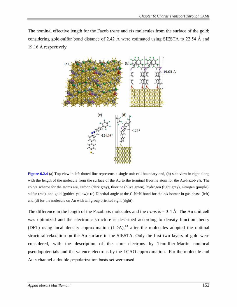
Chapter 6: Charge Transport Through SAMs
Appan Merari Masillamani 152
The nominal effective length for the Fazob trans and cis molecules from the surface of the gold;
considering gold-sulfur bond distance of 2.42 Ǻ were estimated using SIESTA to 22.54 Ǻ and
19.16 Ǻ respectively.
Figure 6.2.4 (a) Top view in left dotted line represents a single unit cell boundary and, (b) side view in right along
with the length of the molecule from the surface of the Au to the terminal fluorine atom for the Au-Fazob cis. The
colors scheme for the atoms are, carbon (dark gray), fluorine (olive green), hydrogen (light gray), nitrogen (purple),
sulfur (red), and gold (golden yellow); (c) Dihedral angle at the C-N=N bond for the cis isomer in gas phase (left)
and (d) for the molecule on Au with tail group oriented right (right).
The difference in the length of the Fazob cis molecules and the trans is ~ 3.4 Ǻ. The Au unit cell
was optimized and the electronic structure is described according to density function theory
(DFT) using local density approximation (LDA),13
after the molecules adopted the optimal
structural relaxation on the Au surface in the SIESTA. Only the first two layers of gold were
considered, with the description of the core electrons by Trouillier-Martin nonlocal
pseudopotentials and the valence electrons by the LCAO approximation. For the molecule and
Au s channel a double ρ+polarization basis set were used.

Chapter 6: Charge Transport Through SAMs
Appan Merari Masillamani 153
For the Au-Fazo trans the molecule has a tilt angle of ~ 7.2° with respect to Au surface normal
(Figure 6.2.2b) while for the Au-Fazo cis (Figure 6.2.4b) the tilt angle is more than the trans
isomer with a value of ~ 16°, this is likely due to the contribution of the bend near the azo group
(-N=N-) which increases the tilt angle. Note that for the Fazob cis the dihedral angle at the –C-
N=N unit is lower than for the molecules packed in the Au-Fazob cis (Figure 6.2.5) this is
possibly due to the intermolecular sterical constraints for between the molecules which prevents
further bending of the molecular backbone.
Figure 6.2.5 Plots illustrating the plane averaged potentials for (a) Au-Fazo trans, free Fazob cis molecular layer
along with the potential profile for Au(111) bulk and (b) Au-Fazo cis, free Fazob trans molecular layer along with
its corresponding Au (111) potential. Green arrows indicate the vacuum level shift arising due to the molecules and
the inverted black arrows refer to the vacuum level offset for the Au-Fazob SAM and the difference between the two
gives the bond dipole. In both the plots the contribution by the five layers of Au can be seen in the distinct profile
potential fluctuations and the contribution due to the molecular system for cis and trans are represented by violet
and red lines respectively.
An estimate of the work function shift can be obtained for the Au-SAM full system under
equilibrium conditions by plotting the plane-averaged electrostatic potential along the normal
axis from the Au surface and superimposing this plot with that of the contribution due to the Au
surface and only the free molecules as shown in Figure 6.2.5.

Chapter 6: Charge Transport Through SAMs
Appan Merari Masillamani 154
The work function shift is due to the contribution of the bond dipole between gold and sulfur
(BDAu-S) and due to the plane average potential difference for the free molecule (ΔVmol) and is
expressed by equation 6.2.1.
molSAu VBD (6.2.1)
The molV is the difference between the left and right plane average potential of the optimized
molecular layer alone excluding the Au surface. The work function for the Au-Fazob cis
estimated from Figure 6.2.5 was 4.96 eV. The shift in the work function due to the Fazob cis free
molecular contribution amounted to -0.28 eV and a bond dipole of 0.66 eV.
The work function shift caused by the Fazob trans is shown in Figure 6.2.5. It was estimated that
the work function shift for the Au-Fazob trans of ~ -0.16 eV arising due to the sum of bond
dipole contribution of 0.52 eV and ΔVFazob trans of -0.68 eV. The work function for the Au- Fazob
trans was calculated to be 5.10 eV, this value was ~ 20 meV greater than that of the Au-Fazob
cis. Table 6.2-1 collects the work function, bond dipole and the plane average potential
difference for Fazob SAMs in both isomeric forms.
Table 6.2-1 Theoretically computed parameters including work function shift induced by Au-Fazob trans and cis
SAMs
6.2.2.2 Ultraviolet photoelectron spectroscopy
Importantly work function estimated by simulations exhibited a similar trend to the
experimentally recorded values by means of ultraviolet photoelectron spectroscopy (UPS) for
both the trans and cis SAMs, wherein the work function of the former was greater than the latter.

Chapter 6: Charge Transport Through SAMs
Appan Merari Masillamani 155
The mean work function values measured with UPS were ~ 5.28 ± 0.01 eV and 4.99 ± 0.08 eV
for the Au-Fazob trans and cis respectively. The conditions used for performing the work
function measurements were a sample scanning energy range from 4.0 to 6.2 eV with a
measurement interval of 0.1 eV and UV spot intensity of 10nW.
To compare the work function shift induced by the chemisorption of the Fazob molecules the
work function of pristine Au electrode immersed in chloroform for 24h was recorded and it
amounted to 5.08 ± 0.02 eV. The work function of the electrodes was extracted from the
minimum threshold energy after which the emission of photo excited electrons occur from the
ground energy state (Figure 6.2.6).
Figure 6.2.6 Square root of photoelectron emission yield as a function of scan energy for Fazob SAMs on Au/mica
(a) trans and (b) cis forms. The dotted lines are the linear fits from which the x-axis intercept gives the work
function of the Au-SAM.
The work function difference (ΔФ) between Fazob trans and cis of ~290 meV has a good
agreement with the theoretically simulated estimates, although being a factor of two higher. This
modest deviation can be accounted to the inherent defects in the Fazob SAMs of the
experimental samples, as opposed to the ideal ordering and packing of the SAMs taken for the
theoretical computations.

Chapter 6: Charge Transport Through SAMs
Appan Merari Masillamani 156
6.2.2.3 Contact potential difference of Fazob SAMs on Au
By means of macroscopic Kelvin probe the contact potential difference (CPD) for the SAMs of
Fazob in trans and cis forms on gold was monitored over 5 different sets of measurements over a
duration of 12h. The duration of each measurement was ~20 min and the sequence in which the
CPD was recorded was in the order of bare Au, Au-Fazo cis and Au-Fazob trans. Taking the
difference between the contact potential difference for the Au-trans (ΔCPDtrans-Au) or cis
(ΔCPDcis-Au) SAMs to that of the bare Au revealed that there was ~+80 to +120 mV shift for
Fazob trans SAM. The ΔCPDcis-Au was reduced from -100 to -30 mV over 12h (Figure 6.2.7b)
suggesting that the gradual thermal recovery of the molecules in the cis form back to that
thermodynamically stable trans form.7 The work function changed from 5.15 to 5.26 eV and 5.34
to 5.40 eV for Au-Fazob cis and Au-Fazo trans SAMs respectively with time.
Figure 6.2.7 Contact potential difference between (a) Fazob trans and cis SAMs on Au, (b) SAMs in both isomeric
forms with respect to Au reference sample.
The variation in the ΔCPD with time becomes apparent by taking the difference of the CPD for
both the trans and cis (ΔCPDtrans-cis) states. The ΔCPDtrans-cis spanned from initial value of 190
mV and dropped to 140 mV (Figure 6.2.7a).

Chapter 6: Charge Transport Through SAMs
Appan Merari Masillamani 157
6.2.2.4 Comparison of different techniques
The difference in work function between the Au-Fazob trans and cis SAMs were ~ 290 meV. It
must be noted that the simulated values of the work function were best estimates for an ideal
packing of the Fazob molecules in both isomeric forms on the Au(111) surface, but in reality due
to the inherent structural defects present in the Fazob SAMs causes the deviation in the observed
experimental values.
The observed contact potential difference of 190 to 140 mV for the Au-Fazob trans and cis
SAMs again clearly provides a quantitative proof that the work function of the Au electrode
modified by the Fazob molecules in the cis form is lower than the trans. The CPD which was
recorded in ambient conditions probes the potential difference induced by the difference in the
capacitance formed by the vibrating metallic tip over the sample. This method which is a non-
contact technique can thus be employed to monitor the change in CPD over an extended interval
a time without causing changes in the chemical composition of the surface. The ΔФ between the
Au-Fazob trans and cis measured by KP revealed a value in range of ~190 to 140 meV.
Remarkably the lower bounds of the difference in work function of the Au-Fazob trans and cis
SAMs matched closely to the theoretically predicted difference. More crucially the trend in the
work function values of gold modified by Fazob recorded experimentally and calculated
theoretically showed remarkable consistency, such that the Ф of the trans SAM was always
greater than the cis by at least 140 meV.
6.2.3 Conclusions
The theoretical study work function for a system of fluorinated azobenzene SAMs on Au(111)
with trans and cis forms revealed that the work function shift and the work function of the Au-
Fazob trans was greater than the Au-Fazob cis by ~ 120 and 140 meV respectively. The
experimentally measured values for the Fazob SAMs in both isomeric forms showed a difference
of nearly 290 meV when the trans form was coated to the Au surface than the cis. The similar
work function trend for the simulated and measured values proves the robustness of the
fluorinated azobenzene self-assembled system on flat gold substrates across completely diverse
techniques.

Chapter 6: Charge Transport Through SAMs
Appan Merari Masillamani 158
Outlooks: Directions for extended work
With the understanding of the work function shift for Fazob SAM on Au, we wanted to
investigate the effect of structural modifications theoretically of the starting molecule (Figure
6.2.8a) upon replacement of fluorine atoms with hydrogen atoms in the ortho (Figure 6.2.8b) and
meta (Figure 6.2.8c) positions respectively.
Figure 6.2.8 Scheme of the chemical structure of (a) Fazob trans, (b) Fazob without fluorine in ortho position of
terminal phenyl ring (FazobnoFO trans), and (c) Fazob without fluorine in meta position of terminal phenyl ring
(FazobnoFM trans).
Theoretical simulations were performed for the both the Fazob without fluorine in ortho position
(abbreviated as FazobnoFO trans) and in meta position of terminal phenyl ring (abbreviated as
FazobnoFM trans) with the similar packing on the Au(111) cell as shown in Figure 6.2.2. The
work function shifts were estimated for the respective optimized structures and are summarized
in Table 6.2-2.
On close observation of the results from the simulations, it is clear that there is a dramatic
influence in the work function of the Au-Fazob trans when the fluorine atoms are removed and
replaced with hydrogen atoms in the ortho positions resulting in a total work function shift of ~ -
0.79 eV. The contribution to this huge shift in the work function arises mainly from the potential
difference in the FazobnoFO trans free molecular layer with a value of ~ -1.41 eV. In contrast to
the work function shift to the FazobnoFO the FazobnoFM SAM exhibited the opposite total shift
of ~ 0.27 eV.

Chapter 6: Charge Transport Through SAMs
Appan Merari Masillamani 159
Table 6.2-2. Summary of parameters extracted from theoretical simulations for the Fazob SAMs on Au with
different structural alterations to the starting Fazob molecule. The negative sign in front of work function shift as
vacuum level offset.
Au-SAM parameters
Fazob
trans Fazob
cis Fazob noFO
trans Fazob noFM
trans E
ads (eV) -4.42 -4.26 -4.36 -4.35
Ф (eV) 5.10 4.96 4.48 5.54 ΔФ (eV) -0.16 -0.28 -0.79 0.27 ΔV
mol (eV) -0.68 -0.94 -1.41 -0.35
Bond dipole (D) -1.21 -0.97 -1.13 -1.13 Bond dipole (eV) 0.52 0.66 0.62 0.62
It is interesting that the bond dipole of the Fazob trans molecules with or without the removal of
fluorine atoms remains fairly constant with a value of 0.62 eV, this suggests that the effective
change in the work function shift mainly arises due to the replacement of fluorine by hydrogen in
respective positions of the terminal phenyl ring.
Figure 6.2.9 Work function values of the Fazob SAM on Au(111) based on theoretical simulations. The trans form
of the molecule in indicated with red and cis isomer with violet bars respectively. The corresponding structure of the
free molecule is overlaid in the plot for clarity.
These results quite clearly show that simple structural modifications can play a very significant
role in fluorine terminated azobenzene SAMs as evidenced by the work function difference of >1

Chapter 6: Charge Transport Through SAMs
Appan Merari Masillamani 160
eV for the Au-FazobnoFO trans (Ф ≈ 4.48 eV) and Au- FazobnoFM trans (Ф ≈ 5.54 eV). Figure
6.2.9 shows the work function values of all the systems studied thus far, currently simulations are
underway to obtain the work function values for the Fazob cis with the replacement of fluorine in
both ortho and meta positions similar to the trans isomeric case.
6.2.4 References
1 Griffiths, J. II. Photochemistry of azobenzene and its derivatives. Chem. Soc. Rev. 1, 481-493
(1972).
2 Sekkat, Z., Wood, J. & Knoll, W. Reorientation mechanism of azobenzenes within the trans.
fwdarw. cis photoisomerization. J. Phys. Chem. 99, 17226-17234 (1995).
3 Ikeda, T. & Tsutsumi, O. Optical Switching and Image Storage by Means of Azobenzene Liquid-
Crystal Films. Science 268, 1873-1875, (1995).
4 Tamai, N. & Miyasaka, H. Ultrafast Dynamics of Photochromic Systems. Chem. Rev. 100, 1875-
1890, (2000).
5 Qune, L. F. N. A., Akiyama, H., Nagahiro, T., Tamada, K. & Wee, A. T. S. Reversible work
function changes induced by photoisomerization of asymmetric azobenzene dithiol self-
assembled monolayers on gold. Appl. Phys. Lett. 93, 083109-083103 (2008).
6 Nagahiro, T., Akiyama, H., Hara, M. & Tamada, K. Photoisomerization of azobenzene containing
self-assembled monolayers investigated by Kelvin probe work function measurements. J.
Electron. Spectrosc. Relat. Phenom. 172, 128-133, (2009).
7 Crivillers, N. et al. Photoinduced work function changes by isomerization of a densely packed
azobenzene-based SAM on Au: a joint experimental and theoretical study. PCCP 13, 14302-
14310 (2011).
8 Crivillers, N. et al. Large Work Function Shift of Gold Induced by a Novel Perfluorinated
Azobenzene-Based Self-Assembled Monolayer. Adv. Mater. 25, 432-436 (2013).
9 Ferri, V. et al. Light-powered electrical switch based on cargo-lifting azobenzene monolayers.
Angew Chem Int Edit 47, 3407-3409, (2008).
10 Mativetsky, J. M. et al. Azobenzenes as Light-Controlled Molecular Electronic Switches in
Nanoscale Metal−Molecule−Metal Junctions. J. Am. Chem. Soc. 130, 9192-9193, (2008).
11 Crivillers, N., Orgiu, E., Reinders, F., Mayor, M. & Samorì, P. Optical Modulation of the Charge
Injection in an Organic Field-Effect Transistor Based on Photochromic Self-Assembled-
Monolayer-Functionalized Electrodes. Adv. Mater. 23, 1447-1452, (2011).
12 Pace, G. et al. Cooperative light-induced molecular movements of highly ordered azobenzene
self-assembled monolayers. Proceedings of the National Academy of Sciences 104, 9937-9942,
(2007).
13 Rusu, P. C. & Brocks, G. Work functions of self-assembled monolayers on metal surfaces by
first-principles calculations. Phys. Rev. B 74, 073414 (2006).

Chapter 6: Charge Transport Through SAMs
Appan Merari Masillamani 161
6.3 CHARGE TRANSPORT THROUGH SELF-ASSEMBLED MONOLAYERS OF FLUORINATED AZOBENZENE ON AU
ELECTRODES
In the part of the chapter the charge transport through self-assembled monolayers (SAMs) on
gold of two different fluorinated azobenzene derivatives is reported. The difference in tunneling
rates when the azobenzene molecule undergoes photo isomerization is investigated by means of
measurements in a two terminal setup comprising of liquid metallic gallium-indium as the top
probe electrode. Based on the switching pattern of the azobenzene molecules in solution between
two photo-stationary states the samples were prepared separately via ex-situ preparation in both
trans and cis isomeric forms and characterized as prepared.
6.3.1 Motivation
The assembly of thiol based molecules on noble metal such as gold surfaces by auto organization
provides a viable route to realize densely packed, ordered single molecular thick (or thin in the
realistic sense) 2D crystalline films. This self-assembly is driven by the affinity of the thiol
molecules to form a strong covalent type of bond with the Au surface and occurs by the process
termed as chemisorption (i.e., chemical adsorption).1,2
Making use of self-assembly selective
molecules with appropriate anchoring atoms can be adsorbed onto the surface of noble metals to
change its work function, wettability properties and charge injection in a device. In other words a
specified pre-programmed function based on the intrinsic structure and property of the molecule
can deliver a customized function once assembled onto metallic electrodes such as gold. The use
of photochromic molecules such as azobenzene in SAMs on Au adds in electronic bi-
functionality to entire system owing to the property of azobenzene to undergo photo induced
reversible isomerization. In essence it behaves as a bistable switch, wherein one state can act as
an ON (lower resistive component with respect to the other state) and the other state performing
the opposite OFF (higher resistive component) operation due to change in the tunneling
resistances induced by the molecule in the two different isomeric forms. This property of
azobenzene SAMs has been exploited to demonstrate electrical current switching on Au
electrodes3,4
and also work function modification of electrodes in devices.5-9
Here we study the

Chapter 6: Charge Transport Through SAMs
Appan Merari Masillamani 162
charge transport through novel fluorinated azobenzene derivatives assembled onto gold
electrodes in both its isomeric forms.
6.3.2 Results and discussions
6.3.2.1 Optical properties of fluorinated azobenzene solution
The chemical structures of the two different azobenzene derivatives used in this study are
depicted in the inset of Figure 6.3.1. The fluorinated azobenzene molecule is abbreviated as Fazo
(Figure 6.3.1 inset) and the azobenzene with two phenyl rings is either end of the azo (-N=N-)
group is termed as Fazob (see inset of Figure 6.3.1).
To understand time necessary to induced complete isomerization from the trans to cis forms in
solution for both Fazo and Fazob we performed standard UV-vis absorption spectroscopy. The
absorption spectrum of 10µM Fazo and Fazob solution in CHCl3 was obtained from wavelength
range of 300 to 600 nm by either UV or white light in the long lateral face of the cuvette
containing the solution.
For the Fazo solution the absorption spectrum was recorded in intervals of 10, 10, 10, 30, 60, 120
s respectively while irradiating with UV light (8 W power intensity at a fixed distance) at λ of
365 nm between successive measurements. After 120 s from the initial time the spectrum
saturated reaching its photo-stationary state, irradiation of another 120 s with UV did not change
the resulting spectrum thus confirming that 120 s was sufficient to convert the molecules to the
cis isomeric form. The reverse switching back to the initial trans state of the Fazo molecule was
obtained by irradiation with white light at intervals of 10, 10, 30, 60 s respectively. After 110 s of
white light irradiation the molecules adopted the trans state, which was observed by the recovery
of the initial absorption characteristics of the Fazo solution. The photo isomerization duration for
cis → trans was as expected greater than trans → cis since the trans isomer is the more
thermodynamically favorable among the two species. Two distinct isosbestic points were
observed at λ of 321.1 and 430.4 nm respectively.
For the Fazob solution the absorption spectrum was recorded in intervals of 10, 10, 40, 60 s
respectively while irradiating with UV light at λ of 365 nm between each measurement. The
spectrum saturated reaching its photo-stationary state after 80 s, further irradiation of another 60

Chapter 6: Charge Transport Through SAMs
Appan Merari Masillamani 163
s with UV resulted in no noticeable change in the spectrum thus confirming that a minimum
duration of 80 s UV irradiation was sufficient to convert the molecules to the cis isomeric form.
Further UV irradiation after 140 s yielded no changed in the spectrum.
Figure 6.3.1 UV-vis spectrum of Fazo solution from (a) trans to cis, and (b) cis to trans and of Fazob solution (c)
trans to cis, and (b) cis to trans. The chemical structure the molecules are represented as the inset of (a) Fazo and (c)
Fazob. The isosbestic points are indicated with green circles and the red oval shows the spectrum after 24h cooling
in a refrigerator.
To switch the molecules back to its trans isomeric form irradiation with white light at intervals
of 10, 10, 30 s respectively. It was observed that after 50 s of white light irradiation the
molecules adopted the trans state, this was evident upon overlaying the initial spectrum with the
photo converted trans spectrum.

Chapter 6: Charge Transport Through SAMs
Appan Merari Masillamani 164
Again for the Fazob solution similar to Fazo, the photo isomerization duration for cis → trans
was as expected greater than trans → cis since the trans isomer is the more thermodynamically
favorable among the two species. There were two distinct isosbestic points at λ of 311.2 and
417.1 nm respectively.
The major difference along the differences in the isosbestic points between the Fazo and Fazob
solution were, (1) the absorption peak in the initial trans isomeric form of Fazob was 354.1 nm
which was nearly 10 nm blue shifted in comparison to Fazo with peak of 364.1 nm, (2) the
transition offset wavelength window between the isosbestic points for Fazo of 109.3 nm was
moderately larger than Fazob 105.9 nm and (3) the profile of the absorption minima of Fazo
within the isosbestic points was much flatter and suppressed with the disappearance of the peak
than for Fazob which showed the presence of a clear peak. These major differences between
Fazo and Fazob in solution are due to the relative dipole moments induced by the molecule and
its interaction with the surrounding solvent environment.
Figure 6.3.2 (a) Illustration of a simplified model of azobenzene photo isomerization process, the possible
mechanism of transition from trans to cis and the reverse process is shown. (b) Scheme showing the change in the
molecular confirmation of Fazob in trans isomeric form to cis confirmation upon ex-situ UV irradiation of Fazo
solution and subsequent chemisorption of Fazob cis species directly to form Au-Fazob cis SAM. The Fazob cis
molecules adsorbed onto gold does not retain a large bend in the azo group due to the steric repulsion between
fluorine atoms of adjacent molecules at the tail of the SAM.
The simplified transition mechanism from trans to cis occurs by the absorption of photon (Figure
6.3.2) from the energy of the UV light after which the azobenzene molecule gets excited to the
intermediate excited state and after which it relaxes to the ground state in the cis isomeric form.10

Chapter 6: Charge Transport Through SAMs
Appan Merari Masillamani 165
The cross section of absorption of one photon for trans, cis, trans-cis and cis-trans intermediate
states are σt, σc, σtc, σct respectively. The molecules in the cis form apart from being excited by
photons of white light can also undergo thermal relaxation to the trans ground state since the
corresponding energy of the cis isomer is higher than the trans (Figure 6.3.2).
For preparing the SAMs in the trans form clean gold substrates were incubated in 10µM Fazo
and Fazob solutions for 24h. The preparation of the SAMs in cis isomeric form involved first
irradiation of the respective Fazo and Fazob solutions with UV light for duration of 240 or 140 s
respectively to fully photo isomerize the molecules to cis form after which the gold substrates
was immersed in this solution and the sample along with the solution was kept inside a
refrigerator at 4°C in dark for 24h. This Fazo or Fazob solution still predominantly contained
molecules in the cis form in solution after 24h according to the UV-vis spectrums (Figure 6.3.1).
Thus this method of preparation of the SAM in the cis form is termed as ex-situ. After removal
from the respective solutions after 24h the substrates were rinsed thoroughly with CHCl3 solvent.
6.3.2.2 Electrical characterization of Fazo and Fazob SAMs
We employed the eutectic alloy of gallium-indium (GaInE) which due to intrinsic nature to
behave like a non-Newtonian liquid could be employed as a soft probe over the layer of SAM to
record the charge transport properties. In other words the GaInE
can conform to the profile of the
surface of the SAM without altering the underlying structure. The GaInE bulk can be molded into
a conical shaped tip which could be employed as the non-intrusive top contact on the SAM.
Nomenclature of junctions: We denote the junctions formed with the following naming
convention, Au-SAM/Ga2O3||GaInE where “-” denotes a covalently bound contact, “/” the
physical contact between the gallium oxide with the SAM and “||” the interface between the
gallium oxide (Ga2O3) layer and the GaInE bulk. Figure 6.3.3 shows the schematic of a junction
of Fazob trans SAM sandwiched between Au and GaInE
electrodes along with the biasing
conditions.
A single channel source measure unit (SMU) served as the potential source (Keithley 2635)
interfaced with the two terminal junctions by means of a triaxial cable to minimize leakage
losses. For all junctions the applied DC potential sweep was from -0.5V → +0.5V (unidirectional

Chapter 6: Charge Transport Through SAMs
Appan Merari Masillamani 166
I-V trace) and for the bidirectional bias sweep the potential direction followed -0.5V → +0.5V →
-0.5V. The entire setup was housed in a custom built Faraday cage to reduce the electrostatic
discharge (ESD).
Figure 6.3.3 Schematic illustration of an Au-Fazob trans/Ga2O3||GaInE
junction along with the biasing
configuration. The Au substrate is held at electrical ground, while the potential is applied to the GaInE electrode.
The charge transport across the SAMs are quantified by means of the current density (J) obtained
for the each of the formed junctions. The outcome for a single measurement is a current vs.
voltage (I-V) trace which is further processed to obtain the actual J which is a function of the
junction bias. Then normalization of I recorded for each measurement over the corresponding
area of the junction yields J. Much number of measurements were performed in different
junctions and at varied regions of the sample and multiple samples to arrive at a reasonable
consensus of the range of distribution of the current density through a particular SAM. The J
generally tends to have a log-normal type of distribution this is attributed to the exponential
relationship with distance of charge tunneling.
The charge transport measurement results for the Fazob trans SAM plotted as log|J| histogram is
shown in Figure 6.3.4. In total histogram for Fazob trans SAM the histogram comprises of 78
log|J| recorded values taken at a bias of -0.4V. The histogram is fitted with a gaussian fit where
the peak of the gaussian curve indicating the mean log|J|, which gives the most probable
occurrence for log|J| over the entire distribution this value, was estimated to be -1.8 ± 0.5 in
log|J| magnitude (J = 15.7 mA/cm2 ).

Chapter 6: Charge Transport Through SAMs
Appan Merari Masillamani 167
Figure 6.3.4 Histogram indicating the frequency of occurrence of log|J| recorded for Fazob trans form SAM on Au
extracted at a bias of -0.4V. The number of occurrences of log|J| (Jobs) in this histogram is indicated.
Shown in Figure 6.3.5 is the log|J| distribution for the Fazob cis SAM constituting 121 log|J|
observations (Jobs) in total. The mean in log|J| magnitude was estimated to be -1.6 ± 0.4 which
corresponds to a mean J value of 26.7 mA/cm2.
Figure 6.3.5 Log|J| distribution for Au-Fazob cis SAM at a bias of -0.4V fitted with a Gaussian curve.
The mean log|J| vs. V profile for the Fazob SAMs on both isomeric forms on Au is shown in
Figure 6.3.6. The mean log|J| for the shorter cis is greater than that of the trans isomer, this is
due to the lower amount of tunneling resistance induced by the shorter cis SAM than the longer
trans.4

Chapter 6: Charge Transport Through SAMs
Appan Merari Masillamani 168
Figure 6.3.6 The current density vs. junction bias profile for the Fazob SAMs on Au in both trans and cis forms. The
mean value of J is depicted for clarity. The dotted line at -0.4 V represent the potential value from which the log|J|
histograms were populated.
The charge transport measurements through the Fazo SAMs on gold were carried out similar to
the procedure outlined above for the Fazob SAMs. The log|J| distribution at a bias value of -0.4
V for Fazo trans and cis SAMs is illustrated in and the corresponding mean log|J| vs. V profile is
shown in Figure 6.3.7.
Figure 6.3.7 (a) log|J| distribution at -0.4 V for junctions of Au-Fazo trans/Ga2O3||GaInE (top) and Au-Fazo
cis/Ga2O3||GaInE (top), the total number of observations in the histograms are represented appropriately. (b)
Variation of mean log|J| with junction bias for the Fazo SAMs on gold, the dotted lines at -0.4 V illustrates the point
in the J-V profile from which the values of the log|J| histograms are populated from.
-0.6 -0.4 -0.2 0.0 0.2 0.4 0.6
-5
-4
-3
-2
-1
cis
trans
log
|J|
Ac
m-2
Junction bias (V)

Chapter 6: Charge Transport Through SAMs
Appan Merari Masillamani 169
For the Fazo SAM in the trans form the mean of log|J| magnitude from a total of 103 Jobs
amounted to -1.7±0.3 which equates to a mean J of 18.3 mA/cm2. While for the Fazo cis SAM
the observed mean log|J| at a junction bias of -0.4 V was -1.4±0.4 from 129 Jobs and its
equivalent mean current density was 44.5 mA/cm2.
6.3.2.3 Discussions
The charge transport across SAMs based on conjugated molecules follows a relationship
described as Simmons model which gives the relationship between the charge density, the
tunneling decay and the distance. The Simmons model in the simplified form is given by
deJJ 0 where β gives the exponential decay due to increase in the charge tunneling length d
and J0 is the current density which might be expected in a hypothetical case when the tunneling
distance is 0.3,11-13
Since the charge transport in the molecular monolayer is governed by the molecular length, we
estimated the individual length of the Fazob molecule both in the trans and cis isomeric forms
(Figure 6.3.8) to be 22.5 Å and 19.11Å respectively, this is taking into account the Au-S bond
linkage distance of 2.36Å. In the case of Fazob trans the length is estimated from the Au to the
terminal fluorine atom when the molecule is in its full extended form (Figure 6.3.8), while for
Fazob cis the length is considered to be from the Au to the fluorine atom in the ortho position of
the terminal phenyl ring (Figure 6.3.8). So in principle in considering that the charge tunneling
through the Fazob trans and cis SAMs is dominated by the distance dependence of tunneling, the
J for the Fazob trans should be lower than the shorter length SAM based on Fazo cis. The
extracted value of J for Fazob trans SAMs after the statistical data analysis yielded a values in
the range of 5.4x10⁻³
– 45.9 x10⁻³
A/cm2
and 10.6 – 67.6 mA/cm2
for the Fazo cis SAM which
results in a factor of ~2 to 1.5 higher J in the lower and upper bound limits respectively for the
shorter cis. The lower and upper bounds of the log|J| reported here are taken from one standard
deviation width of the log-normal distribution. The statistical analysis and the plotting of
histogram was performed using ggplot2 package14
in R.15
It is expected that in the case of conjugated molecules through Fazo and Fazob SAMs on gold
the charge transport is through bond non-resonant tunneling.4,16
The charge tunneling decay

Chapter 6: Charge Transport Through SAMs
Appan Merari Masillamani 170
through the Fazob SAM can be estimated by plotting the mean of the log|J| vs. the distance of
tunneling. The β estimated from the slope of the plot shown in amounted to 0.16Å-1
.
Figure 6.3.8 Illustration of length of Fazo molecule adsorbed on gold in (a) trans and (b) cis isomeric form. Similar
representation of the Fazob molecules chemisorbed on gold in (c) trans and (d) cis. In the case of cis isomers for
both Fazo and Fazob the length was estimated from the Au surface to the fluorine atom pointing upwards in the
terminal phenyl ring in the ortho position.
The lengths of the Fazo SAMs chemisorbed on gold surface similar to the Fazob SAMs were
estimated from theoretical simulations after optimization of the molecules packed onto the
surface of gold. The optimization algorithm considers the highest probable tilt angle based of
repeated iterations and the length thus estimated reflects the true value which might be the case
for the ideal ordered packing of the molecules.
Figure 6.3.9 log|J| vs. distance plots showing the tunneling decay observed for Fazob SAMs on Au. The dashed line
is the linear least square fit.

Chapter 6: Charge Transport Through SAMs
Appan Merari Masillamani 171
The Fazo SAM length for trans and cis isomeric forms were 18.1Å and 14.2 Å respectively. The
current density values at lower and upper bound of single standard deviation for Fazo trans
SAMs were in the range of 8.9 – 37.6 mA/cm
2 and 18.1 – 109.5 mA/cm
2 for the Fazo cis SAM.
The lower and upper limits within 68% confidence interval of the log|J| distribution of Fazo cis
was two to three fold greater than the trans SAM. The tunneling decay between the two isomers
of Fazo SAM was then extracted from the slope of the log|J| vs. d plot (Figure 6.3.10) was
0.23Å-1
and is the range reported in the literature for systems of π-conjugated molecular based
SAMs.12,16
Figure 6.3.10 Variation of the log|J| with distance for Fazo SAMs on Au. The corresponding trans and cis SAMs
are depicted adjacent to its mean log|J| values. The error bar represents denote one standard deviation interval and
dashed line is the linear fit.
Influence of defects in the monolayer: SAMs on Au adopting both trans and cis confirmation
of either Fazo or Fazob can have defects in the monolayer due to inherent defects such as grain
boundaries, step edges on the Au supporting substrate along with defects caused by adventitious
materials adsorbed to either the Au or GaInE
electrodes and also due to steric repulsive effects of
between adjacent molecules during SAM formation (Figure 6.3.11). The deviation from the ideal
dense uniform ordering of the molecules in the SAM is also one of the major reasons for the
larger span of log|J| distributions.

Chapter 6: Charge Transport Through SAMs
Appan Merari Masillamani 172
Figure 6.3.11 Cartoon showing the possible arrangements or defects in Au-Fazo trans/Ga2O3||GaInE junctions.
The defects can significantly influence the overall outcome of the charge transport measurements in SAMs.

Chapter 6: Charge Transport Through SAMs
Appan Merari Masillamani 173
6.3.3 References
1 Nuzzo, R. G. & Allara, D. L. Adsorption of bifunctional organic disulfides on gold surfaces. J.
Am. Chem. Soc. 105, 4481-4483 (1983).
2 Ulman, A. Formation and structure of self-assembled monolayers. Chem. Rev. 96, 1533 (1996).
3 Ferri, V. et al. Light-powered electrical switch based on cargo-lifting azobenzene monolayers.
Angew Chem Int Edit 47, 3407-3409, (2008).
4 Mativetsky, J. M. et al. Azobenzenes as Light-Controlled Molecular Electronic Switches in
Nanoscale Metal−Molecule−Metal Junctions. J. Am. Chem. Soc. 130, 9192-9193, (2008).
5 Qune, L. F. N. A., Akiyama, H., Nagahiro, T., Tamada, K. & Wee, A. T. S. Reversible work
function changes induced by photoisomerization of asymmetric azobenzene dithiol self-
assembled monolayers on gold. Appl. Phys. Lett. 93, 083109-083103 (2008).
6 Nagahiro, T., Akiyama, H., Hara, M. & Tamada, K. Photoisomerization of azobenzene containing
self-assembled monolayers investigated by Kelvin probe work function measurements. J.
Electron. Spectrosc. Relat. Phenom. 172, 128-133, (2009).
7 Crivillers, N. et al. Photoinduced work function changes by isomerization of a densely packed
azobenzene-based SAM on Au: a joint experimental and theoretical study. PCCP 13, 14302-
14310 (2011).
8 Crivillers, N., Orgiu, E., Reinders, F., Mayor, M. & Samorì, P. Optical Modulation of the Charge
Injection in an Organic Field-Effect Transistor Based on Photochromic Self-Assembled-
Monolayer-Functionalized Electrodes. Adv. Mater. 23, 1447-1452, (2011).
9 Lazzerini, G. M. et al. Increased efficiency of light-emitting diodes incorporating anodes
functionalized with fluorinated azobenzene monolayers and a green-emitting polyfluorene
derivative. Appl. Phys. Lett. 101, 153306-153305 (2012).
10 Sekkat, Z., Wood, J. & Knoll, W. Reorientation mechanism of azobenzenes within the trans.
fwdarw. cis photoisomerization. J. Phys. Chem. 99, 17226-17234 (1995).
11 Ho Choi, S., Kim, B. & Frisbie, C. D. Electrical Resistance of Long Conjugated Molecular Wires.
Science 320, 1482-1486, (2008).
12 Masillamani, A. M. et al. Multiscale Charge Injection and Transport Properties in Self-
Assembled Monolayers of Biphenyl Thiols with Varying Torsion Angles. Chem. Eur. J. 18,
10335-10347, (2012).
13 Reus, W. F. et al. Statistical Tools for Analyzing Measurements of Charge Transport. J. Phys.
Chem. C 116, 6714-6733, (2012).
14 Wickham, H. ggplot2: elegant graphics for data analysis. (Springer, 2009).
15 R Development Core Team. R: A language and environment for statistical computing. (Springer,
2011).
16 Kronemeijer, A. et al. Electrical characteristics of conjugated self-assembled monolayers in large-
area molecular junctions. Appl. Phys. Lett. 97, 173302 (2010).


Chapter 6: Charge Transport Through SAMs
Appan Merari Masillamani 175
6.4 TRANSMISSION STUDIES THROUGH SINGLE MOLECULE AZOBENZENE DERIVATIVES LINKING GOLD ELECTRODES
Aim
To study the electronic transport through an azobenzene based molecular wires attached to gold
leads. The transmission through the molecule changes with the strength of the linker group with
the electrode and if there is physisorption or the presence of a small gap is introduced at one side
of the junction, the transmission through the junction is expected to drop significantly due to the
weak electronic coupling. In the project we aim to investigate how the transmission varies
through different structural and geometrical configurations of single azobenzene molecules
linking gold electrodes.
6.4.1 Motivation
The azobenzene molecule undergoes reversible photoisomerization from thermodynamically
stable fully extended trans form to cis upon selective excitation with appropriate electromagnetic
wavelength. The same azobenzene molecule also exhibits distinct conductive state between the
two isomers. Here we investigate the transmission through the azobenzene molecule covalently
linked to gold electrodes (Figure 6.4.1).
Figure 6.4.1 Schematic illustration of azobenzene molecule between periodic Au(111) surface in trans and cis
isomeric states.
6.4.2 Provisional results
The system under investigation comprises of a left electrode (L), azobenezene (azo) as a
molecular wire and right electrode (R). Sulfur was the linker to both the electrode. We consider

Chapter 6: Charge Transport Through SAMs
Appan Merari Masillamani 176
equilibrium conditions wherein the charge screening is neutral for the entire system of the Au
electrodes along with the azobenezene. The Fermi level is constant at equilibrium and the
conductance through the molecule can be estimated from Landauer formula given by,
hETe F /)(2 2 (6.4.1)
Where T(EF) is the transmission coefficient through the molecule as a function of the Fermi
energy (EF). Using DFT the effective potentials were estimated. The transmission coefficients
through the azo in trans along with the eigenstates of the molecular self-projected Hamiltonian
(MPSH) is shown in Figure 6.4.2. The transmission at EF for Au-azo trans-Au was 0.06 while for
Au-azo cis-Au was 0.013. The transmission coefficients through the azo in cis along with the
eigenstates of MPSH levels is shown in Figure 6.4.3.
Figure 6.4.2. Transmission coefficients through the Au-azo trans-Au along with the molecular self-projected
Hamiltonian levels depicted with green bars (left panel). Charge density localization along the Au-azo trans-Au
system, the corresponding MPSH levels are labeled and indicated with respective arrows. The red and the turquoise
lobes are the orbital projections.
The broad transmission close to the EF for both the trans and cis azo suggests the transport
through the Au-azo-Au with molecules in both isomeric states are due to resonant tunneling
mechanism. The ratio of the transmission from trans to cis is ca. 4.6 which suggests that at the
Fermi energy the trans state is more conductive than the cis.

Chapter 6: Charge Transport Through SAMs
Appan Merari Masillamani 177
Figure 6.4.3 Transmission coefficients through the Au-azo cis-Au along with respective MPSH levels as green bars
(left panel). Charge density localization along the Au-azo cis-Au system, the corresponding MPSH levels are labeled
and indicated with respective arrows. In the right panel the orbital projections are portrayed in the red and turquoise
colors.
The highest occupied molecular orbital (HOMO) and lowest unoccupied molecular orbital
charge localization of the azo molecules in the gas phase is represented in Figure 6.4.4.
Figure 6.4.4 Optimized molecular structure of the azo in the gas phase in cis and trans states (left), corresponding
HOMO and LUMO orbital charge localization lobes are displayed in the middle and right respectively.
On closer inspection of the transmission spectrum and on comparison of the MPSH levels with
the HOMO and LUMO levels of the molecule in the gas phase we can note that there is a Fermi
level pinning effect induced when the azo molecule is linked to the gold electrodes. Figure 6.4.5

Chapter 6: Charge Transport Through SAMs
Appan Merari Masillamani 178
shows the comparative plot of the HOMO-LUMO levels in the gas phase and Au-azo-Au. The
HOMO LUMO gap for the free azo molecule upon covalent linkage to the Au electrode is lower
indicating a Fermi level pinning of gold-azo which vanishes in the gas phase of the molecules.
Figure 6.4.5 Comparison the HOMO and LUMO levels of the azo molecules in gas phase and between Au
electrodes, illustrating the pinning effect upon attachment with gold. The dashed line represents the Fermi level of
gold-azo.
The study of transmission through the azobenzene was extended to other derivatives such as
fluorinated azobenzene monothiol (Fazo2, see Figure 6.4.6a), and biphenyl variant dithiol
(Fazo3, see Figure 6.4.6) and monothiol (Fazo3|Au, see Figure 6.4.6c).
Figure 6.4.6 Different configuration of azobenzene between gold electrodes (a) Monothiol linked only to bottom
electrode, (b) biphenyl variant linked to both electrodes, (c) monothiol linked to bottom electrode. All azobenzene
derivatives are depicted in their trans and cis isomeric forms.

Chapter 6: Charge Transport Through SAMs
Appan Merari Masillamani 179
The summary of the transmission coefficient spectrum from simulations is illustrated in Figure
6.4.7. All these transmission was calculated considering no bias (0 V) between the electrodes.
Figure 6.4.7 Change in transmission through the different azobenzene molecule linked to gold electrodes.
The magnitude of the transmission when there is monothiol is around 3 orders of magnitude
lower at the Fermi level in the trans, this is due to the weak orbital overlap into the gold
electrode near the gap.
Currently simulations are underway to estimate transmission through all these junctions
considering bias applied to the electrodes.


Chapter 7: Epilogue
Appan Merari Masillamani 181
Reason's last step is the recognition that there are an infinite number of things which are beyond it.
-Blaise Pascal (1623-1662), Polymath
7 Epilogue
7.1 CONCLUSIONS AND OUTLOOKS
In this thesis the complete aspects of charge transport in organic π-conjugated molecular based
systems were studied. The immediate impacts of this field of research are manifold, wherein the
techniques employed to study the charge transport in prototypical OFETs would pave the way
forward in the development of more efficient organic devices by greater control over/ improving
understanding of:
(1) The device channel by the incorporation of solution processed polymer gate dielectrics of a
specific molecular weight which enhances carrier mobility by better matching the surface
properties at the semiconductor/dielectric interface.
(2) The switching stability over extended periods of operation by employing dielectrics with a
good breakdown strength and low leakage losses combined with lower amount of dipolar surface
defects.
(3) The understanding of the rate of charge carrier trapping provides a deep insight into the
mechanism governing this phenomenon from which vital clues and design considerations can be
deduced, for the development of transistors with high reliability.
(4) Charge injection from electrodes by chemisorption of molecules with different geometries
and functional groups. The molecules used to form monolayers on electrodes can be tailored to
maximize the carrier injection efficiency by minimizing the hole/electron injection barrier to the
transport HOMO/LUMO levels. This aspect has profound implications in a wide array of devices
from organic light emitting diodes, organic photovoltaic along with transistors. Moreover each of
the electrodes can be functionalized with different molecules thereby creating asymmetry
between the charge injecting and collecting electrodes which would facilitate the realization of
complementary logic circuits over large areas with a single semiconductor active layer.

Chapter 7: Epilogue
Appan Merari Masillamani 182
5) The tuning of the intrinsic properties of charge transport in single component1 organic
semiconductor integrated as the active layer in a device by customized pre deposition and post
processing methods.
(6) Charge transport modulation of the conductivity of a pristine semiconductor upon addition of
extrinsic dopant type of photo-tunable small molecules. The entire paradigm governing intrinsic
charge transport properties of the starting semiconductor compound can be dramatically altered
by controlled blending with photochromic molecules. This creates a viable platform to envisage
completely new functionalities for the bicomponent systems such as optical sensing,
optoelectronic switching and photo induced memory effects.
(7) Mixing two or more components can be done solely to enhance the efficiency of one
component at the expense of sacrificing performance of others. In other words blending can be
constructively competitive for a single preferential component while detrimental to the
remaining compounds. The other approach could involve cooperative effect wherein all the
isolated compounds when combined together either enhance the function of one component or
allow the emergence of multiple yet distinct functionalities in a single material or a device. The
properties of molecular orientation, arrangement and rearrangement upon blending, phase
separation, inter component physical-mechanical-electronic-chemical interactions, selective
response to distinct external stimuli, affinity between the entire ensemble of compounds with the
substrate and electrodes are some of the issues which should be considered for designing multi-
responsive devices.
(8) The incorporation of photo responsive self-assembled monolayers (SAMs) as one of the
building blocks in organic electronic devices makes it tractable to modulate certain functions
within the device without affecting the performance of another part. For instance, the optical
stimuli can be precisely localized to a specific region of a larger area panel with varied
combination of devices to control the electrical output state of one device, which might be
supplied as the input signal to completely different electronic device in the same panel.
1 This can comprise of any single one of the following compounds such as long chain polymers (and copolymers),
shorter oligomers or small molecules possessing semiconductive properties.
Chapter 7: Epilogue
Appan Merari Masillamani 183
(9) How structural modifications of thiol based molecules chemisorbed on gold to form SAMs
influence the electronic function such as charge transport rates and conductivities. The premise
that practically infinitely diverse molecular geometries can be used to alter the electronic
function based on the structure opens up countless opportunities to tune the work function of
electrodes, charge injection properties and electrical current switching states.
7.2 GENERAL LONG-TERM PERSPECTIVES AND DIRECTIVES
Controlled blending to achieve optimal intermixing and minimal inter component interfacial
defects can be taken a step further by combining more than two different components comprised
of energetically favorable properties of transport levels in donor/acceptor, though this might
increase the complexity of the underlying charge transport. If this can be fully mastered, this
could potentially play a major role in improving efficiency in the organic solar cells by greater
charge separation and collection with lower recombination losses.
Embedding photo responsive SAMs in distinct regions of large scale electronic circuits can be
supplemented by employing multiple stimulations simultaneously or with a controlled time lag at
different wavelengths2 of excitation directly over appropriate molecules spatially isolated. The
output signals of which can be modulated by the external photo induced stimuli the logical states
of the output can be then either combined or multiplexed to perform customized digital logic
functions. The main advantage of using photochromic molecules in SAMs thus can be fully put
to use in extremely low weight and ultra-low power consuming sensors, nanoscale motion
detectors, molecular motors and machines.
The dielectric constant of the polymeric dielectrics film could be increased significantly by
addition of nanoparticles at different ratios. The incorporation of high permittivity dielectrics
makes it plausible to conceive organic transistors with very low operating power.
Looking at the wider picture the molecular electronics can diversify into the fields of
nanobiotechnology. Here individual molecules or a set of molecules grouped in a nanodevice
which can be used to attach to a malignant tumor for example in a biological specimen and this
device could be controlled by a wireless signal to scavenge cell samples or to destroy locally the
2 This is referred to target molecule(s) oriented excitation wavelength, which would de distinct to each of the
different molecular structures depending of the optical spectral signature.

Chapter 7: Epilogue
Appan Merari Masillamani 184
cancerous cells. The rates of charge tunneling in healthy cells and cancerous cells could also be
studied to potentially find solutions for preventive and alternative treatments.
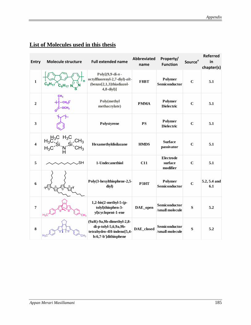
Appendix
Appan Merari Masillamani 185
List of Molecules used in this thesis
Entry Molecule structure Full extended nameAbbreviated
name
Property/
FunctionSource
a
Referred
in
chapter(s)
1
Poly[(9,9-di-n -
octylfluorenyl-2,7-diyl)-alt -
(benzo[2,1,3]thiadiazol-
4,8-diyl)]
F8BTPolymer
SemiconductorC 5.1
2Poly(methyl
methacrylate)PMMA
Polymer
DielectricC 5.1
3 Polystyrene PSPolymer
DielectricC 5.1
4 Hexamethyldisilazane HMDSSurface
passivatorC 5.1
5 1-Undecanethiol C11
Electrode
surface
modifier
C 5.1
6Poly(3-hexylthiophene-2,5-
diyl)P3HT
Polymer
SemiconductorC
5.2, 5.4 and
6.1
7
1,2-bis(2-methyl-5-(p-
tolyl)thiophen-3-
yl)cyclopent-1-ene
DAE_openSemiconductor
/small moleculeS 5.2
8
(9aR)-9a,9b-dimethyl-2,8-
di-p-tolyl-5,6,9a,9b-
tetrahydro-4H-indeno[5,4-
b:6,7-b']dithiophene
DAE_closedSemiconductor
/small moleculeS 5.2

Appendix
Appan Merari Masillamani 186
a This denotes how the compound was acquired either from commercial (C) or synthesized (S)
sources.
Entry Molecule structure Full extended nameAbbreviated
name
Property/
FunctionSourcea
Referred
in
chapter(s)
9
2-((2E,2''E,2'''E)-5'''-
(diisocyanomethylene)-
3,3',3''',4''-tetrahexyl-
5H,5'''H-
[2,2':5',2'':5'',2'''-
quaterthiophen]-5-
ylidene)malononitrile
QQT(CN)4Semiconductor
oligomerS 5.3
10 9H-fluorene-2-thiol 5mBPT
small
molecule/electr
ode surface
modifier
S 6.1
119,10-dihydrophenanthrene-
2-thiol6mBPT
small
molecule/electr
ode surface
modifier
S 6.1
12 [1,1'-biphenyl]-4-thiol BPT
small
molecule/electr
ode surface
modifier
S 6.1
132,2'-dimethyl-[1,1'-
biphenyl]-4-thioltBPT
small
molecule/electr
ode surface
modifier
S 6.1
14
(E)-S-(4-((2',3',4',5',6'-
pentafluoro-[1,1'-
biphenyl]-4-
yl)diazenyl)phenyl)
ethanethioate
Fazo
small
molecule/electr
ode surface
modifier
S 6.2
15
(E)-S-(4'-((2',3',4',5',6'-
pentafluoro-[1,1'-
biphenyl]-4-yl)diazenyl)-
[1,1'-biphenyl]-4-yl)
ethanethioate
Fazob
small
molecule/electr
ode surface
modifier
S 6.2 and 6.3

Appendix
Appan Merari Masillamani 187
Logical flow of commands to remotely measure IV trace
I developed the software code to remotely control the electrometer which performs the
application of the bias and records the current values by means of user-defined functions.
Figure 1 shows the time taken for the electrometer to source the bias for the forward and reverse
I-V traces for metal-SAM-metal two terminal junctions.
Figure 1 Time (in seconds) taken by the electrometer to source the bias, with black lines indicating the direction of
electron flow during the potential sweep and red arrows indicates (1) Forward and (2) reverse trace.
Portrayed in Figure 2 is the sequence of the flow of commands followed in the software code to
control the electrometer to perform a bidirectional potential sweep and record the corresponding
current flowing through the junction respectively.

Appendix
Appan Merari Masillamani 188
Figure 2 Logical flow of commands of the software code used to remotely control the electrometer for the
application of forward and reverse potential sweeps and for measuring the respective currents.

List of publications
Appan Merari Masillamani 189
LIST OF PUBLICATIONS
(1) Multiscale Charge Injection and Transport Properties in Self‐Assembled Monolayers of
Biphenyl Thiols with Varying Torsion Angles.
Masillamani Appan Merari, Núria Crivillers, Emanuele Orgiu, Jürgen Rotzler, David Bossert,
Ramakrishnappa Thippeswamy, Michael Zharnikov, Marcel Mayor, and Paolo Samorì.
Chemistry-A European Journal 18, no. 33 (2012): 10335-10347.
(2) Enhanced mobility in P3HT-based OTFTs upon blending with a phenylene–thiophene–
thiophene–phenylene small molecule.
Orgiu, Emanuele, Appan Merari Masillamani, Jörn-Oliver Vogel, Emanuele Treossi, Adam
Kiersnowski, Marcel Kastler, Wojciech Pisula, Florian Dötz, Vincenzo Palermo, and Paolo
Samorì.
Chemical Communications 48, no. 10 (2012): 1562-1564.
(3) Increased efficiency of light-emitting diodes incorporating anodes functionalized with
fluorinated azobenzene monolayers and a green-emitting polyfluorene derivative.
Lazzerini, G. M., S. Mian, F. Di Stasio, A. Merari Masillamani, N. Crivillers, F. Reinders, M.
Mayor, P. Samorì, and F. Cacialli.
Applied Physics Letters 101, no. 15 (2012): 153306-153306.
(4) Molecular weights of polymeric gate dielectrics: role on the stability, reliability and
performance of F8BT based ambipolar OTFTs.
Masillamani Appan Merari, Emanuele Orgiu, Paolo Samorì. (to be submitted soon)
(5) Study of work function of a novel fluorinated azobenzene derivative on Au electrodes.
Masillamani Appan Merari, Osella Silvio, Liscio Andrea, Reinders Federica, Mayor Marcel,
Cornil Jérôme, Paolo Samorì. (Manuscript in preparation)

List of publications
Appan Merari Masillamani 190
(6) Intrinsic carrier mobility of dual mode polymeric semiconductor-photochromic molecular
blend based field effect transistors.
Emanuele Orgiu, Masillamani Appan Merari, Musser Andrew, Friend Richard, Paolo Samorì.
(Manuscript in preparation)
(7) Activation energy of hole carriers in organic field-effect transistors based on Quinoidal
Oligothiophene derivative.
Masillamani Appan Merari, Ribierre Jean-Charles, Emanuele Orgiu, Paolo Samorì. (Manuscript
in preparation)
(8) Charge transport through fluorinated azobenzene self-assembled monolayers on gold
electrode.
Masillamani Appan Merari, Osella Silvio, Reinders Federica, Mayor Marcel, Cornil Jérôme,
Paolo Samorì. (Manuscript in preparation)
(9) Studies of single molecule charge transport through photochromic azobenzene derivatives
linking gold electrodes.
Osella Silvio, Masillamani Appan Merari, Cornil Jérôme, Paolo Samorì. (Manuscript in
preparation)

191
Acknowledgements
It gives me great pleasure to thank Prof. Paolo Samorì who gave me the opportunity and support
to work in his group. He provided me with thought provoking and challenging projects to bring
out the creative best in me which made me a better researcher.
Big credit goes to Prof. Franco Cacialli who instilled in me initial enthusiasm for pursuing
research.
It has been a memorable three years working in this group during which I learnt a lot from fellow
colleagues. Huge credit goes to Dr. Markus Döbbelin for interesting suggestions about science,
life and beyond. Dr. Núria Crivillers has been instrumental in helping me characterize molecular
monolayers, it was really great to work with her. I give credit to Drs. Jeffrey Mativetsky and
Jörn-Oliver Vogel for teaching me the working principles of an Atomic force microscope.
Many projects were successful by the strong support from our collaborators who provided us
with the compounds. To this end I convey my deep gratitude to Drs. Jürgen Rotzler, Federica
Reinders, Mr. David Bossert and Prof. Marcel Mayor from University of Basel, Switzerland who
provided us with the biphenyl thiol and azobenzene compounds. Prof. Jean-Charles Ribierre and
Dr. Florian Dötz provided the quinoidal oligomer and PTTP compounds respectively. My
gratitude goes to Dr. Ramakrishnappa Thippeswamy and Prof. Michael Zharnikov for the
characterization of the biphenyl monolayer on gold.
A special thanks to Mr. Silvio Osella and Dr. Jérôme Cornil for helping me during my
secondment in University of Mons and giving me good advices on how to perform theoretical
computer simulations of molecules on gold surfaces.
It was enriching to work, share and learn from all the members of the team past and present Drs.
Pasquale D’Angelo, Oliver Fenwick, Carlos-Andres Palma, Corinna Raimondo, Andrea
Cadeddu, Matthias Treier, Rebecca Savage, Emanuele Orgiu , Artur Cieseilski along with fellow
doctorate candidates Chiara Musumeci, Maria Del Rosso, Mirella El Gemayel, Tim Leydecker,
Thomas Mosciatti, and Sébastien Haar.

192
On a personal note there are many who I should thank for making me the person who I am today.
I am very grateful to my father and mother who educated me and gave me the values that I stand
for, I would not be here if it was not for your faith in me. Big thanks to my grandmother Mrs.
Selvam Masillamani who keeps me in her well wishes and earnest prayers. I also express my
heartfelt thanks to my good friend Linda, you have been my pillar of support. My sincere thanks
go to my brother, cousins and friends Gaius, Farah, Sneha, Topaz, Ajay, Matthieu, Rohini and
Kutty athai.
Last but not the least I like to acknowledge the Marie Curie fellowship from the European
Commission RTN Threadmill (MRTN-CT-2006-036040) and ITN Superior (PTN-CT-2009-
238177) which enabled me to carry out this research.