
Matrix analysis of metamorphic mineral assemblages and reactions
Metamorphic quantum dots: Quite different nanostructuresL. Seravalli,a� P. Frigeri, L. Nasi, G. Trevisi, and C. BocchiCNR-IMEM, Parco delle Scienze 37a, I-43100 Parma, Italy
�Received 8 June 2010; accepted 27 July 2010; published online 23 September 2010�
In this work, we present a study of InAs quantum dots deposited on InGaAs metamorphic buffersby molecular beam epitaxy. By comparing morphological, structural, and optical properties of suchnanostructures with those of InAs/GaAs quantum dot ones, we were able to evidence characteristicsthat are typical of metamorphic InAs/InGaAs structures. The more relevant are: the cross-hatchedInGaAs surface overgrown by dots, the change in critical coverages for island nucleation andripening, the nucleation of new defects in the capping layers, and the redshift in the emission energy.The discussion on experimental results allowed us to conclude that metamorphic InAs/InGaAsquantum dots are rather different nanostructures, where attention must be put to some issues notpresent in InAs/GaAs structures, namely, buffer-related defects, surface morphology, differentdislocation mobility, and stacking fault energies. On the other hand, we show that metamorphicquantum dot nanostructures can provide new possibilities of tailoring various properties, such as dotpositioning and emission energy, that could be very useful for innovative dot-based devices. © 2010American Institute of Physics. �doi:10.1063/1.3483249�
I. INTRODUCTION
Self-assembled semiconductor quantum dots �QDs� arenanostructures of considerable interest, both from a funda-mental point of view, as they allow to explore properties ofquantum confined carriers, and from a device-oriented per-spective, as they are keys for the development of many in-novative photonic applications such as low-threshold lasers,single photon devices, infrared photodetectors, optical ampli-fiers, and memory devices.1,2 To integrate such structures inthe existing optical fiber technology, it is highly desirable toredshift the emission of QDs into the optoelectronic windowat 1.55 �m. This has been a topic attracting considerableefforts in these last ten years and interesting results havebeen gained by growing QDs on metamorphic buffers.3–8
While some works have discussed in depth the physicalmechanisms that underlay the QD emission redshift9,10 andthe carrier dynamics11 in such structures, considerable lessattention has been paid to differences between metamorphicInAs/InGaAs and InAs/GaAs QD structures. This work aimsat studying the properties of the metamorphic QD systemgrown by molecular beam epitaxy �MBE�, highlighting thedifferences with the GaAs system that require particular carebut that also may provide new opportunities to engineerstructures.
In order to gain a complete picture of characteristicproperties of the metamorphic system, we carried over anoptical �by photoluminescence �PL��, morphological �byatomic force microscopy �AFM��, and structural �by trans-mission electron microscopy �TEM�� study of QD nanostruc-tures, where the coverage was continuously varied across thesample. Comparison between metamorphic InAs/InGaAsstructures and the more investigated InAs/GaAs ones weremade, focusing in particular on the surface on which QDs aregrown, the process of QD nucleation, the onset of structural
defects in the capping layers, and the QD emission depen-dence on coverage. Thanks to the correlation between theresults of different characterizations, some general conclu-sions on metamorphic structures were derived.
While metamorphic structures considered here includetwo different In compositions of InxGa1−xAs buffers �x=0.15 and 0.24�, the main focus of this work is the compari-son between the metamorphic InAs/InGaAs and the InAs/GaAs systems, hence we will refer mainly to the data of thex=0.15 metamorphic structures; nevertheless x=0.24 dataare included for completeness, even if a study of the depen-dence of metamorphic QD properties on InGaAs buffer com-position is beyond the scope of this work.
II. EXPERIMENTAL DETAILS
The samples under investigation consist of InAs QDswith continuously graded coverage �, grown by MBE onmetamorphic InxGa1−xAs, with In compositions x=0.15 and0.24 and on GaAs buffers, that act as lower confining layers�LCLs�. The continuous variation in the amount of depositedInAs was effectively achieved by growing the structures on 2in. substrates, without azimuthal rotation during QD deposi-tion, as described in Ref. 12.
The structures, grown on semi-insulating �100� GaAssubstrates, are composed by: �i� a 100 nm-thick GaAs layergrown at 600 °C, �ii� a 800 nm-thick InxGa1−xAs layergrown at 490 °C, �iii� InAs QDs grown by atomic layermolecular beam epitaxy �ALMBE� at 460 °C with equiva-lent growth rate of 0.15 ML s−1, �iv� a 20 nm InxGa1−xAslayer grown by ALMBE at 360 °C to reduce the intermixingbetween caps and QD layers, and �v� 300 nm of GaAs orInxGa1−xAs grown by MBE at 490 °C. Structures withoutupper layers, grown under the same conditions, were pre-pared for AFM imaging. In this case, after the InAs deposi-tion the substrate temperature was immediately cooled downa�Electronic mail: [email protected].
JOURNAL OF APPLIED PHYSICS 108, 064324 �2010�
0021-8979/2010/108�6�/064324/8/$30.00 © 2010 American Institute of Physics108, 064324-1
Downloaded 11 Oct 2010 to 192.167.161.20. Redistribution subject to AIP license or copyright; see http://jap.aip.org/about/rights_and_permissions

to room temperature. The experimental growth conditions ofInAs/GaAs QD structures are reported in Ref. 12.
As the thickness of the metamorphic InxGa1−xAs LCLsare 800 nm, values of the mismatch between QDs and CLsresult to be 6.27% for x=0.15 and 5.58% for x=0.24, calcu-lated on the basis of the Mareè theory of strain relaxation,13
that has been experimentally confirmed by different tech-niques in Refs. 14 and 15. As in InAs/GaAs structures, themismatch is 7.16%, in these structures the strain felt by QDsis reduced by more than 10% for x=0.15 and 20% for x=0.24.
Contact-mode AFM measurements were performed exsitu by using a Nanoscope III from Digital Instruments.Commercially available silicon cantilevers with conical tipsof nominal curvature radius less than 20 nm were used. TEMinvestigations were performed using JEOL 2200FS and2000FX microscopes working at 200 kV. The analysis ofstructural defects was carried out both in cross sectional andplan view geometries by applying the invisibility criterion indiffraction contrast imaging. The densities of defects as func-tions of coverage were accurately determined using largearea plan view observations with detection sensitivity of 1�107 cm−2 or better. PL spectra were taken at 10 K withexciting light at 532 nm; the spectra were corrected for thespectral response of the setup. The PL spectra were measuredby a Fast-Fourier transform spectrometer with a 1 meV res-olution and a cooled Ge detector.
III. RESULTS
In order to understand how the growth of the metamor-phic buffers affects the properties of InAs QDs, we reporthere on an AFM study comparing morphological features ofInAs islands grown on metamorphic InxGa1−xAs �x=0.15and 0.24� and on GaAs LCLs.
As evidenced from �b� and �c� micrographs in Fig. 1, QDstructures grown on strain-relaxed InGaAs layers show upthe typical undulated surface morphology, known as cross-hatch pattern,16,17 originating from dislocation networks in-troduced at InGaAs/GaAs heterointerface to accommodate
the strain induced by the lattice mismatch. Images of Fig. 1refer to structures with coverages of 2.9 ML; quite similarfeatures are observed over the whole investigated coveragerange.
The development of cross-hatch morphology, with hills
and grooves parallel to the �110� and �1̄10� directions in thecase of structures grown on GaAs �001� substrates, dependson the composition and thickness of the InGaAs layer and isstrongly related to the incorporation process of group III at-oms on growing surface and then to the growth conditions.16
Relatively high growth temperatures �490 °C� and highInxGa1−xAs layer thicknesses �800 nm� might explain thestrong anisotropy between the two orthogonal cross-hatchdirections observed in AFM images and confirmed by cross-
section height profiles along �110� and �1̄10� directions of �e�and �f� panels in Fig. 1. Furthermore, a very noticeable fea-ture highlighted by AFM image �c� in Fig. 1 is the sponta-neous alignment of InAs islands grown on In0.24Ga0.76As
LCL, along the preferential cross-hatch �1̄10� direction.Similar results are reported and discussed in Refs. 18–20 forInAs QDs grown on partially relaxed cross-hatched InGaAstemplates and in Ref. 21, where the authors have proposedthe growth on anisotropic strain-engineered �In,Ga�As super-lattices, as a method to obtain ordering in QD structures.
Moreover, we analyzed the evolution of the density ofInAs islands as a function of coverage, extracted from statis-tical analysis of AFM images. Morphological changes inInAs/GaAs, InAs / In0.15Ga0.85As and InAs / In0.24Ga0.76AsQDs were studied in the 1.6–2.9 ML, 1.4–3.9 ML, and 1.7–3.0 ML range, respectively. Closed and open symbols in Fig.2 refer to the two main dot distributions highlighted by AFMon InAs/GaAs �Ref. 12� and on InAs / In0.15Ga0.85As QDstructures. As reported in Ref. 12, at low coverages, withincreasing � beyond 1.6 ML, the density of InAs islandsgrown on GaAs exhibits a fast increase up to the saturationvalue of �2�1011 islands /cm2 reached for ��2.2 ML.This value remains nearly constant when additional amountof InAs is deposited, however, for ��2.4 ML the analysisof AFM images reveals the nucleation of a second family of
FIG. 1. �Color online� 1.5 �m�1.5 �m AFM images of �a� InAs/GaAs and �b� x=0.15 and �c� x=0.24 metamorphic InAs / InxGa1−xAs QD structures withInAs coverage of 2.9 ML. Blank arrows define start and end points of scan line profiles along �1,1,0� directions reported in panels �d�, �e�, and �f�.
064324-2 Seravalli et al. J. Appl. Phys. 108, 064324 �2010�
Downloaded 11 Oct 2010 to 192.167.161.20. Redistribution subject to AIP license or copyright; see http://jap.aip.org/about/rights_and_permissions

larger-sized islands, open symbols in Fig. 2, coexisting withthe more frequent ones. The occurrence of large-sized InAsislands for high coverages can be explained, as previouslydiscussed in Ref. 12, as a consequence of QD ripening pre-dicted by thermodynamic equilibrium theories of strainedheteroepitaxial systems.22
As for InAs / In0.15Ga0.85As and InAs / In0.24Ga0.76Asmetamorphic QD systems, the evolution of InAs island en-sembles with increasing coverage indicates remarkable dif-ferences with respect to InAs/GaAs QDs. First, by compar-ing the dot density values in low � region of Fig. 2, we findthat the onset of InAs nucleation on metamorphicIn0.15Ga0.85As occurs at lower InAs coverage with respect toGaAs. In the case of In0.24Ga0.76As LCL �not shown in Fig.2�, the investigated coverage range �1.7–3.0 ML� does notallow to study the first stages of island formation, howeverwe expect a further reduction in critical coverage for thetwo-dimensional �2D� to three-dimensional �3D� transition.In fact, this is consistent with the experimental evidenceshowing that in metamorphic systems the amount of InAsrequired to reach the critical thickness for 2D–3D transition,�crit, is reduced when compared to QDs grown on GaAs lay-ers. By observing the streaky-to-spotty reflection high-energy electron diffraction pattern change during the growth,we have estimated a coverage �crit=1.4 ML and 1.2 ML forInAs / In0.15Ga0.85As and InAs / In0.24Ga0.76As, respectively.The observed reduction in �crit, that seems to be in contrastwith the decrease in the lattice mismatch between dot andbuffer layers that has been discussed above, may be relatedto the Indium segregation in the InGaAs layer underlyingInAs QDs. Similar results are reported in previouspapers,20,23 that deal with metamorphic QD structures pre-pared at relatively high growth temperature. The presence onthe surface of In adatom population before the deposition ofthe InAs layer might also explain why the saturation value of�1�1011 islands /cm2 is reached at lower coverages inInAs / InxGa1−xAs �1.7 ML for x=0.15 and presumably lowerfor x=0.24� with respect to InAs/GaAs systems. This couldalso be related to the observation of the reduction in densitysaturation measured in metamorphic structures.
Regarding the high coverage range of Fig. 2, it is worthto note that the critical coverage beyond which ripening oc-curs, is strongly influenced by the presence of the metamor-
phic InGaAs LCLs. This behavior, observed also in Ref. 24,is in agreement with the aforementioned theory,22 which de-scribes the transformation in QD growth mode as a functionof the coverage and of the lattice mismatch between QD andLCLs, predicting that a reduction in the mismatch results in ashift at higher coverages of the onset of ripening. By analyz-ing AFM images, no appreciable changes in dot morphologywere noted up to 2.9 and 3.0 ML in InAs / In0.15Ga0.85As andInAs / In0.24Ga0.76As, respectively. Then, to have evidence ofripening process also in metamorphic QD structures, we ex-tended the investigated coverage range of islands grown onIn0.15Ga0.85As layer up to 3.9 ML. We demonstrated that, forcoverage larger than the critical coverage of 2.9 ML, ripenedislands are clearly visible with a density increasing from 2�108 to 2�109 islands /cm2 reached when �=3.9 ML. Weemphasize here that the study of ripening process inInAs / In0.24Ga0.76As QDs would require exploring too highcoverage, which are not significant for the aims of this re-search.
Figure 3 shows the cross sectional TEM micrograph of atypical InAs / In0.15Ga0.85As structure with InAs coverage �=3.0 ML with the zoom-in view of the QDs, taken with thechemically sensitive �200� reflection, in the inset. A pro-nounced cross-hatch pattern along the �110� direction with aperiodicity consistent with the AFM findings is revealed. Inthese structures misfit dislocations �MDs� are efficiently con-fined at the InGaAs/GaAs interface to accommodate the lat-tice mismatch between the buffer and the substrate. A differ-ent depth distribution of defects was found in theInAs / In0.24Ga0.76As samples, where MDs are also observedto penetrate deeply in the buffer layer. From TEM large-areaplan view investigations, the density of threading disloca-tions starting from the LCL/GaAs interface and reaching thefree surface was estimated to be of the order of 1�108 cm−2 and 7.5�108 cm−2 for InAs / InxGa1−xAs struc-tures with x=0.15 and x=0.24, respectively. It is importantto note that the threading dislocation �TD� density does notdepend on the InAs coverage, as they are related to the bufferproperties and are not influenced by QDs.
It should be noted that the presence of high density ofdislocations in metamorphic structures has been previouslyaddressed and various methods to reduce and control it havebeen put forward, such as the defect reduction technique, theuse of low growth temperatures for InGaAs buffers deposi-tion and the use of step-graded metamorphic layers.5,6
FIG. 2. �Color online� Evolution of InAs island densities for InAs/GaAs�circles� and metamorphic InAs / In0.15Ga0.85As �diamonds� QD structures asa function of the coverage. Open symbols refer to large-sized dot densities.The lines are guides for eyes.
FIG. 3. �1̄10� TEM cross section of InAs / In0.15Ga0.85As QD structure withInAs coverage �=3.0 ML; a V-shaped defect is visible in the cap layer. Inthe inset, the g�200� dark field image of the QDs grown on a ridge of thecross-hatched pattern is reported.
064324-3 Seravalli et al. J. Appl. Phys. 108, 064324 �2010�
Downloaded 11 Oct 2010 to 192.167.161.20. Redistribution subject to AIP license or copyright; see http://jap.aip.org/about/rights_and_permissions
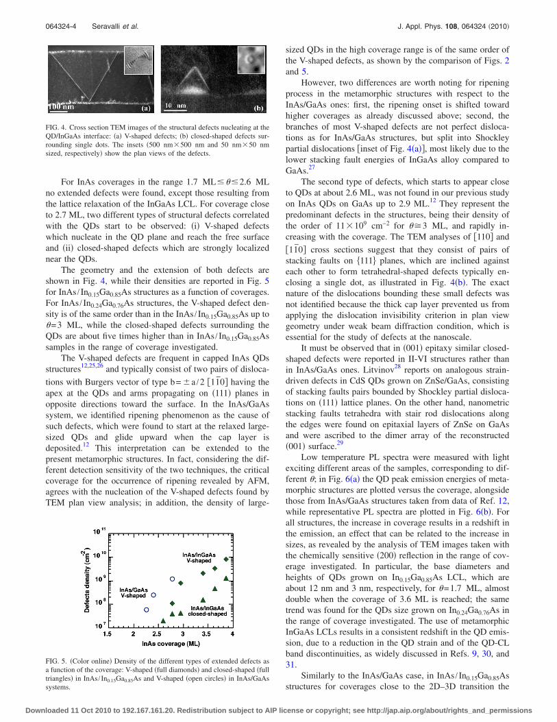
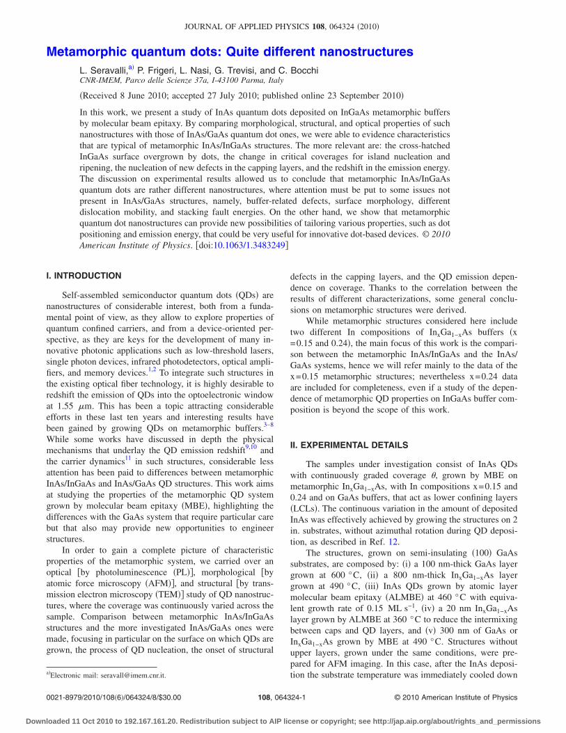
For InAs coverages in the range 1.7 ML���2.6 MLno extended defects were found, except those resulting fromthe lattice relaxation of the InGaAs LCL. For coverage closeto 2.7 ML, two different types of structural defects correlatedwith the QDs start to be observed: �i� V-shaped defectswhich nucleate in the QD plane and reach the free surfaceand �ii� closed-shaped defects which are strongly localizednear the QDs.
The geometry and the extension of both defects areshown in Fig. 4, while their densities are reported in Fig. 5for InAs / In0.15Ga0.85As structures as a function of coverages.For InAs / In0.24Ga0.76As structures, the V-shaped defect den-sity is of the same order than in the InAs / In0.15Ga0.85As up to�=3 ML, while the closed-shaped defects surrounding theQDs are about five times higher than in InAs / In0.15Ga0.85Assamples in the range of coverage investigated.
The V-shaped defects are frequent in capped InAs QDsstructures12,25,26 and typically consist of two pairs of disloca-
tions with Burgers vector of type b= �a /2 �11̄0� having theapex at the QDs and arms propagating on �111� planes inopposite directions toward the surface. In the InAs/GaAssystem, we identified ripening phenomenon as the cause ofsuch defects, which were found to start at the relaxed large-sized QDs and glide upward when the cap layer isdeposited.12 This interpretation can be extended to thepresent metamorphic structures. In fact, considering the dif-ferent detection sensitivity of the two techniques, the criticalcoverage for the occurrence of ripening revealed by AFM,agrees with the nucleation of the V-shaped defects found byTEM plan view analysis; in addition, the density of large-
sized QDs in the high coverage range is of the same order ofthe V-shaped defects, as shown by the comparison of Figs. 2and 5.
However, two differences are worth noting for ripeningprocess in the metamorphic structures with respect to theInAs/GaAs ones: first, the ripening onset is shifted towardhigher coverages as already discussed above; second, thebranches of most V-shaped defects are not perfect disloca-tions as for InAs/GaAs structures, but split into Shockleypartial dislocations �inset of Fig. 4�a��, most likely due to thelower stacking fault energies of InGaAs alloy compared toGaAs.27
The second type of defects, which starts to appear closeto QDs at about 2.6 ML, was not found in our previous studyon InAs QDs on GaAs up to 2.9 ML.12 They represent thepredominant defects in the structures, being their density ofthe order of 11�109 cm−2 for ��3 ML, and rapidly in-creasing with the coverage. The TEM analyses of �110� and
�11̄0� cross sections suggest that they consist of pairs ofstacking faults on �111 planes, which are inclined againsteach other to form tetrahedral-shaped defects typically en-closing a single dot, as illustrated in Fig. 4�b�. The exactnature of the dislocations bounding these small defects wasnot identified because the thick cap layer prevented us fromapplying the dislocation invisibility criterion in plan viewgeometry under weak beam diffraction condition, which isessential for the study of defects at the nanoscale.
It must be observed that in �001� epitaxy similar closed-shaped defects were reported in II-VI structures rather thanin InAs/GaAs ones. Litvinov28 reports on analogous strain-driven defects in CdS QDs grown on ZnSe/GaAs, consistingof stacking faults pairs bounded by Shockley partial disloca-tions on �111� lattice planes. On the other hand, nanometricstacking faults tetrahedra with stair rod dislocations alongthe edges were found on epitaxial layers of ZnSe on GaAsand were ascribed to the dimer array of the reconstructed�001� surface.29
Low temperature PL spectra were measured with lightexciting different areas of the samples, corresponding to dif-ferent �; in Fig. 6�a� the QD peak emission energies of meta-morphic structures are plotted versus the coverage, alongsidethose from InAs/GaAs structures taken from data of Ref. 12,while representative PL spectra are plotted in Fig. 6�b�. Forall structures, the increase in coverage results in a redshift inthe emission, an effect that can be related to the increase insizes, as revealed by the analysis of TEM images taken withthe chemically sensitive �200� reflection in the range of cov-erage investigated. In particular, the base diameters andheights of QDs grown on In0.15Ga0.85As LCL, which areabout 12 nm and 3 nm, respectively, for �=1.7 ML, almostdouble when the coverage of 3.6 ML is reached; the sametrend was found for the QDs size grown on In0.24Ga0.76As inthe range of coverage investigated. The use of metamorphicInGaAs LCLs results in a consistent redshift in the QD emis-sion, due to a reduction in the QD strain and of the QD-CLband discontinuities, as widely discussed in Refs. 9, 30, and31.
Similarly to the InAs/GaAs case, in InAs / In0.15Ga0.85Asstructures for coverages close to the 2D–3D transition the
FIG. 4. Cross section TEM images of the structural defects nucleating at theQD/InGaAs interface: �a� V-shaped defects; �b� closed-shaped defects sur-rounding single dots. The insets �500 nm�500 nm and 50 nm�50 nmsized, respectively� show the plan views of the defects.
FIG. 5. �Color online� Density of the different types of extended defects asa function of the coverage: V-shaped �full diamonds� and closed-shaped �fulltriangles� in InAs / In0.15Ga0.85As and V-shaped �open circles� in InAs/GaAssystems.
064324-4 Seravalli et al. J. Appl. Phys. 108, 064324 �2010�
Downloaded 11 Oct 2010 to 192.167.161.20. Redistribution subject to AIP license or copyright; see http://jap.aip.org/about/rights_and_permissions
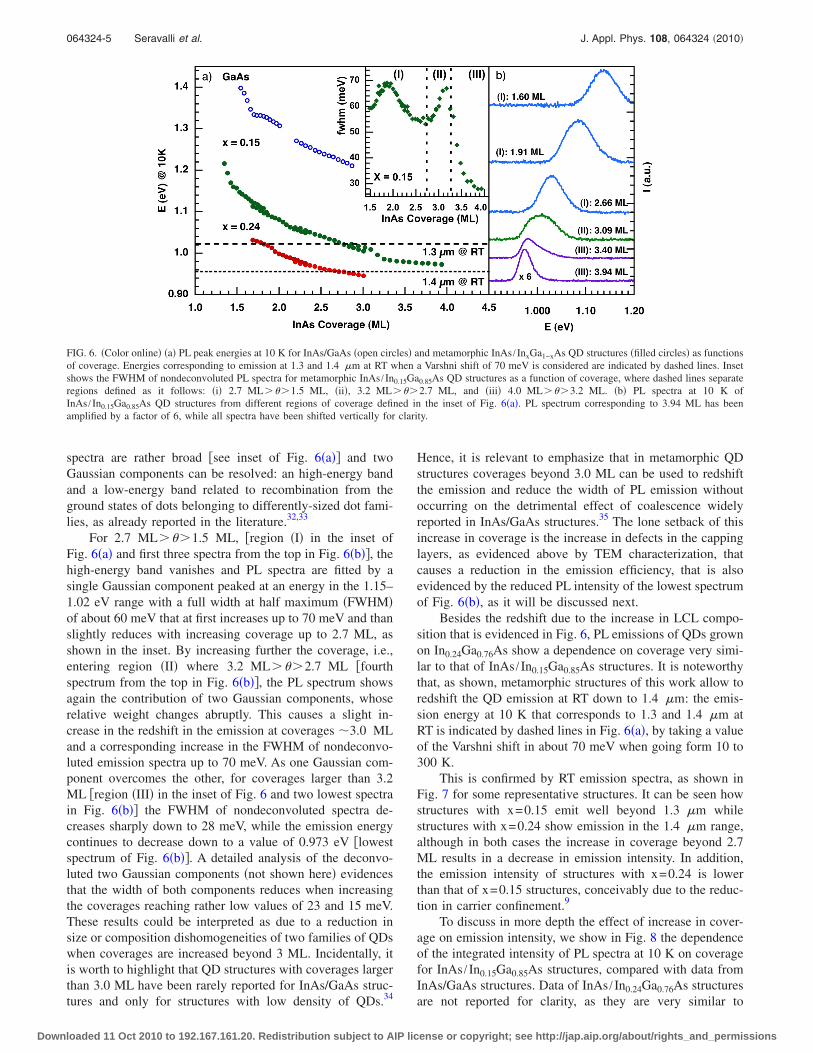
spectra are rather broad �see inset of Fig. 6�a�� and twoGaussian components can be resolved: an high-energy bandand a low-energy band related to recombination from theground states of dots belonging to differently-sized dot fami-lies, as already reported in the literature.32,33
For 2.7 ML���1.5 ML, �region �I� in the inset ofFig. 6�a� and first three spectra from the top in Fig. 6�b��, thehigh-energy band vanishes and PL spectra are fitted by asingle Gaussian component peaked at an energy in the 1.15–1.02 eV range with a full width at half maximum �FWHM�of about 60 meV that at first increases up to 70 meV and thanslightly reduces with increasing coverage up to 2.7 ML, asshown in the inset. By increasing further the coverage, i.e.,entering region �II� where 3.2 ML���2.7 ML �fourthspectrum from the top in Fig. 6�b��, the PL spectrum showsagain the contribution of two Gaussian components, whoserelative weight changes abruptly. This causes a slight in-crease in the redshift in the emission at coverages �3.0 MLand a corresponding increase in the FWHM of nondeconvo-luted emission spectra up to 70 meV. As one Gaussian com-ponent overcomes the other, for coverages larger than 3.2ML �region �III� in the inset of Fig. 6 and two lowest spectrain Fig. 6�b�� the FWHM of nondeconvoluted spectra de-creases sharply down to 28 meV, while the emission energycontinues to decrease down to a value of 0.973 eV �lowestspectrum of Fig. 6�b��. A detailed analysis of the deconvo-luted two Gaussian components �not shown here� evidencesthat the width of both components reduces when increasingthe coverages reaching rather low values of 23 and 15 meV.These results could be interpreted as due to a reduction insize or composition dishomogeneities of two families of QDswhen coverages are increased beyond 3 ML. Incidentally, itis worth to highlight that QD structures with coverages largerthan 3.0 ML have been rarely reported for InAs/GaAs struc-tures and only for structures with low density of QDs.34
Hence, it is relevant to emphasize that in metamorphic QDstructures coverages beyond 3.0 ML can be used to redshiftthe emission and reduce the width of PL emission withoutoccurring on the detrimental effect of coalescence widelyreported in InAs/GaAs structures.35 The lone setback of thisincrease in coverage is the increase in defects in the cappinglayers, as evidenced above by TEM characterization, thatcauses a reduction in the emission efficiency, that is alsoevidenced by the reduced PL intensity of the lowest spectrumof Fig. 6�b�, as it will be discussed next.
Besides the redshift due to the increase in LCL compo-sition that is evidenced in Fig. 6, PL emissions of QDs grownon In0.24Ga0.76As show a dependence on coverage very simi-lar to that of InAs / In0.15Ga0.85As structures. It is noteworthythat, as shown, metamorphic structures of this work allow toredshift the QD emission at RT down to 1.4 �m: the emis-sion energy at 10 K that corresponds to 1.3 and 1.4 �m atRT is indicated by dashed lines in Fig. 6�a�, by taking a valueof the Varshni shift in about 70 meV when going form 10 to300 K.
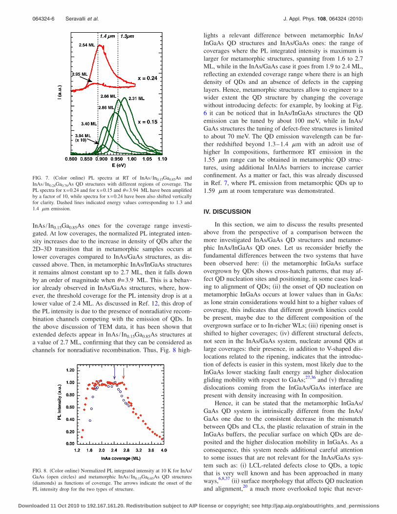
This is confirmed by RT emission spectra, as shown inFig. 7 for some representative structures. It can be seen howstructures with x=0.15 emit well beyond 1.3 �m whilestructures with x=0.24 show emission in the 1.4 �m range,although in both cases the increase in coverage beyond 2.7ML results in a decrease in emission intensity. In addition,the emission intensity of structures with x=0.24 is lowerthan that of x=0.15 structures, conceivably due to the reduc-tion in carrier confinement.9
To discuss in more depth the effect of increase in cover-age on emission intensity, we show in Fig. 8 the dependenceof the integrated intensity of PL spectra at 10 K on coveragefor InAs / In0.15Ga0.85As structures, compared with data fromInAs/GaAs structures. Data of InAs / In0.24Ga0.76As structuresare not reported for clarity, as they are very similar to
FIG. 6. �Color online� �a� PL peak energies at 10 K for InAs/GaAs �open circles� and metamorphic InAs / InxGa1−xAs QD structures �filled circles� as functionsof coverage. Energies corresponding to emission at 1.3 and 1.4 �m at RT when a Varshni shift of 70 meV is considered are indicated by dashed lines. Insetshows the FWHM of nondeconvoluted PL spectra for metamorphic InAs / In0.15Ga0.85As QD structures as a function of coverage, where dashed lines separateregions defined as it follows: �i� 2.7 ML���1.5 ML, �ii�, 3.2 ML���2.7 ML, and �iii� 4.0 ML���3.2 ML. �b� PL spectra at 10 K ofInAs / In0.15Ga0.85As QD structures from different regions of coverage defined in the inset of Fig. 6�a�. PL spectrum corresponding to 3.94 ML has beenamplified by a factor of 6, while all spectra have been shifted vertically for clarity.
064324-5 Seravalli et al. J. Appl. Phys. 108, 064324 �2010�
Downloaded 11 Oct 2010 to 192.167.161.20. Redistribution subject to AIP license or copyright; see http://jap.aip.org/about/rights_and_permissions
InAs / In0.15Ga0.85As ones for the coverage range investi-gated. At low coverages, the normalized PL integrated inten-sity increases due to the increase in density of QDs after the2D–3D transition that in metamorphic samples occurs atlower coverages compared to InAs/GaAs structures, as dis-cussed above. Then, in metamorphic InAs/InGaAs structuresit remains almost constant up to 2.7 ML, then it falls downby an order of magnitude when �=3.9 ML. This is a behav-ior already observed in InAs/GaAs structures, where, how-ever, the threshold coverage for the PL intensity drop is at alower value of 2.4 ML. As discussed in Ref. 12, this drop ofthe PL intensity is due to the presence of nonradiative recom-bination channels competing with the emission of QDs. Inthe above discussion of TEM data, it has been shown thatextended defects appear in InAs / In0.15Ga0.85As structures ata value of 2.7 ML, confirming that they can be considered aschannels for nonradiative recombination. Thus, Fig. 8 high-
lights a relevant difference between metamorphic InAs/InGaAs QD structures and InAs/GaAs ones: the range ofcoverages where the PL integrated intensity is maximum islarger for metamorphic structures, spanning from 1.6 to 2.7ML, while in the InAs/GaAs case it goes from 1.9 to 2.4 ML,reflecting an extended coverage range where there is an highdensity of QDs and an absence of defects in the cappinglayers. Hence, metamorphic structures allow to engineer to awider extent the QD structure by changing the coveragewithout introducing defects: for example, by looking at Fig.6 it can be noticed that in InAs/InGaAs structures the QDemission can be tuned by about 100 meV, while in InAs/GaAs structures the tuning of defect-free structures is limitedto about 70 meV. The QD emission wavelength can be fur-ther redshifted beyond 1.3–1.4 �m with an adroit use ofhigher In compositions, furthermore RT emission in the1.55 �m range can be obtained in metamorphic QD struc-tures, using additional InAlAs barriers to increase carrierconfinement. As a matter or fact, this was already discussedin Ref. 7, where PL emission from metamorphic QDs up to1.59 �m at room temperature was demonstrated.
IV. DISCUSSION
In this section, we aim to discuss the results presentedabove from the perspective of a comparison between themore investigated InAs/GaAs QD structures and metamor-phic InAs/InGaAs QD ones. Let us reconsider briefly thefundamental differences between the two systems that havebeen observed here: �i� the metamorphic InGaAs surfaceovergrown by QDs shows cross-hatch patterns, that may af-fect QD nucleation sites and positioning, in some cases lead-ing to alignment of QDs; �ii� the onset of QD nucleation onmetamorphic InGaAs occurs at lower values than in GaAs:as lone strain considerations would hint to a higher values ofcoverage, this indicates that different growth kinetics couldbe present, maybe due to the different composition of theovergrown surface or to In-richer WLs; �iii� ripening onset isshifted to higher coverages; �iv� different structural defects,not seen in the InAs/GaAs system, nucleate around QDs atlarge coverages: their presence, in addition to V-shaped dis-locations related to the ripening, indicates that the introduc-tion of defects is easier in this system, most likely due to theInGaAs lower stacking fault energy and higher dislocationgliding mobility with respect to GaAs;27,36 and �v� threadingdislocations coming from the InGaAs/GaAs interface arepresent with density increasing with In composition.
Hence, it can be stated that the metamorphic InGaAs/GaAs QD system is intrinsically different from the InAs/GaAs one due to the consistent decrease in the mismatchbetween QDs and CLs, the plastic relaxation of strain in theInGaAs buffers, the peculiar surface on which QDs are de-posited and the higher dislocation mobility in InGaAs. As aconsequence, this system needs additional careful attentionto some issues that are not relevant for the InAs/GaAs sys-tem such as: �i� LCL-related defects close to QDs, a topicthat is very well known and has been approached in manyways,6,8,37 �ii� surface morphology that affects QD nucleationand alignment,20 a much more overlooked topic that never-
FIG. 7. �Color online� PL spectra at RT of InAs / In0.15Ga0.85As andInAs / In0.24Ga0.76As QD structures with different regions of coverage. ThePL spectra for x=0.24 and for x=0.15 and �=3.94 ML have been amplifiedby a factor of 10, while spectra for x=0.24 have been also shifted verticallyfor clarity. Dashed lines indicated energy values corresponding to 1.3 and1.4 �m emission.
FIG. 8. �Color online� Normalized PL integrated intensity at 10 K for InAs/GaAs �open circles� and metamorphic InAs / In0.15Ga0.85As QD structures�diamonds� as functions of coverage. The arrows indicate the onset of thePL intensity drop for the two types of structure.
064324-6 Seravalli et al. J. Appl. Phys. 108, 064324 �2010�
Downloaded 11 Oct 2010 to 192.167.161.20. Redistribution subject to AIP license or copyright; see http://jap.aip.org/about/rights_and_permissions

theless could have significant implications and could deservesome studies focusing for example on the effects of LCLcomposition and growth parameters, and �iii� different dislo-cation mobility and stacking fault energies in InGaAs cap-ping layers that could affect the strain relaxation rates andmechanisms of QDs in metamorphic structures, an argumentwhich was never explored up to now and could deserve fur-ther studies in order to clarify the role of the different defectsin the strain release process.
On the other hand, at the same time the metamorphicsystem provides additional possibilities to design structures:�i� QD strain and confinement can be engineered9,31 allowingfor tuning of emission, control of activation energies and ofother physical parameters, �ii� wider range of coverageswithout defects in the capping layers can be used, thanks tothe lower value of the onset of QD nucleation and the higherone for the threshold of defect nucleation, �iii� QD nucle-ation and alignment could be controlled to some extent, tak-ing advantage of the dependence of the onset of nucleationon LCL properties and of the cross-hatch patterns character-istics on the InGaAs LCL, and �iv� PL emission is observablefrom QDs with coverages larger than 3.0 ML.
As an example of potentialities of metamorphic QDstructures, let us now consider the tuning of QD emissionwavelength in the 1.3 �m region: in Refs. 9, 30, and 31 itwas widely discussed how QD strain engineering allows totune the QD emission by acting on metamorphic LCLs’ com-position and thickness, without changing the QD coverage.Here we consider the change in coverage and LCL compo-sition: by looking at Fig. 6 it can be seen that QD emissioncan be tuned in the range 1.3–1.4 �m at RT by using bothx=0.15 and 0.24: let us compare the two cases with theiradvantages and disadvantages. In the first case�InAs / In0.15Ga0.85As structures� a coverage larger than 2.8ML would be required, meaning that structures would havedefects in the capping layers close to QDs and reduced PLintensity. On the positive side, structures would have a lowdensity of threading dislocations coming from the InGaAsLCL and a higher confinement energy for carriers �due tohigher QD-CL band discontinuity for CLs with lower Incomposition� with regards to InAs / In0.24Ga0.76As structures.Moreover, coverages larger than 3 ML could be used, takingadvantage of the increase in QD sizes and of the reduction insize dishomogeneity to obtain narrower PL spectra with red-shifted emission. If LCLs with x=0.24 were to be used,lower coverages should be considered allowing to avoid de-fect nucleation close to QDs and providing the maximumlight emission efficiency. On the other hand, carriers wouldbe less confined and metamorphic LCLs would have anhigher density of defects.
V. CONCLUSIONS
In conclusion, in this work MBE-grown metamorphicInAs / InxGa1−xAs QD nanostructures were characterized byAFM, TEM, and PL in order to compare their properties tothose of the more common InAs/GaAs QD system. We evi-denced how the metamorphic structures have some charac-teristic properties that make them a rather different system
such as: the cross-hatched surface on which QDs are depos-ited, the dependence of the 2D–3D transition on buffer com-position, the change in the onset of defect nucleation in theInGaAs capping layers and the appearance of new defectssurrounding the QDs in capping layers. We discussed howmetamorphic QDs can give opportunities not present inInAs/GaAs structures to tune the QD emission in the win-dows of optoelectronic interest, by taking advantage of theredshift due to the reduction in QD strain and QD-CL banddiscontinuities, of the wider range of coverages that allowsfor maximum light emission efficiency and of the possibilityof using coverages larger than 3.0 ML. Moreover, the depen-dence of the 2D–3D transition on the buffer compositioncould suggest approaches to control more efficiently the QDnucleation and alignment. On the other hand, in this type ofstructures one should be aware of issues such as the presenceof defects coming from the LCL-GaAs interface, the effectsof the surface morphology on QD properties and the reduc-tion in carrier confinement. We think that these results dem-onstrate that metamorphic QDs are a very different system incomparison with the InAs/GaAs one and that their typicalfeatures can provide interesting new potentialities for the de-sign of QD structures. This should be of interest for the QDcommunity in order to widen the engineering potentialitieson QDs and on their physical properties.
ACKNOWLEDGMENTS
The work has been partially supported by the “SANDiE”Network of Excellence of EU under Contract No. NMP4-CT-2004-500101. The AFM characterization has been carriedout at CIM, University of Parma.
1D. Bimberg, Semiconductor Nanostructures �Springer, Berlin, 2008�.2M. Henini, Handbook of Self Assembled Semiconductor Nanostructuresfor Novel Devices in Photonics and Electronics �Elsevier, Amsterdam,London, 2008�.
3G. Balakrishnan, S. Huang, T. Rotter, A. Stintz, L. Dawson, K. Malloy, H.Xu, and D. Huffaker, Appl. Phys. Lett. 84, 2058 �2004�.
4T. Kettler, L. Karachinsky, N. Ledentsov, V. Shchukin, G. Fiol, M. Kuntz,A. Lochmann, O. Schulz, L. Reissmann, K. Posilovic, D. Bimberg, I.Novikov, Y. Shernyakov, N. Gordeev, M. Maksimov, N. Kryzhanovskaya,A. Zhukov, E. Semenova, A. Vasil’ev, V. Ustinov, and A. Kovsh, Appl.Phys. Lett. 89, 041113 �2006�.
5L. Karachinsky, T. Kettler, I. I. Novikov, Y. M. Shernyakov, N. Y.Gordeev, M. V. Maksimov, N. Kryzhanovskaya, A. E. Zhukov, E. S. Se-menova, A. P. Vasil’ev, V. M. Ustinov, G. Fiol, M. Kuntz, A. Lochmann,O. Schulz, L. Reissmann, K. Posilovic, A. R. Kovsh, S. S. Mikhrin, V. A.Shchukin, N. N. Ledentsov, and D. Bimberg, Semicond. Sci. Technol. 21,691 �2006�; N. N. Ledentsov, V. A. Shchukin, T. Kettler, K. Posilovic, D.Bimberg, L. Y. Karachinsky, A. G. Gladyschev, M. V. Maksimov, I. I.Novikov, Y. M. Shernyakov, A. E. Zhukov, V. M. Ustinov, and A. R.Kovsh, J. Cryst. Growth 301, 914 �2007�.
6Z. Mi and P. Bhattacharya, IEEE J. Sel. Top. Quantum Electron. 14, 1171�2008�.
7L. Seravalli, P. Frigeri, G. Trevisi, and S. Franchi, Appl. Phys. Lett. 92,213104 �2008�.
8H. Liu, Y. Qiu, C. Jin, T. Walther, and A. Cullis, Appl. Phys. Lett. 92,111906 �2008�.
9L. Seravalli, M. Minelli, P. Frigeri, S. Franchi, G. Guizzetti, M. Patrini, T.Ciabattoni, and M. Geddo, J. Appl. Phys. 101, 024313 �2007�.
10S. Ghanad-Tavakoli, A. Naser, D. Thompson, and M. Jamal Deen, J. Appl.Phys. 106, 063533 �2009�.
11S. Sanguinetti, D. Colombo, M. Guzzi, E. Grilli, M. Gurioli, L. Seravalli,P. Frigeri, and S. Franchi, Phys. Rev. B 74, 205302 �2006�.
12P. Frigeri, L. Nasi, M. Prezioso, L. Seravalli, G. Trevisi, E. Gombia, R.
064324-7 Seravalli et al. J. Appl. Phys. 108, 064324 �2010�
Downloaded 11 Oct 2010 to 192.167.161.20. Redistribution subject to AIP license or copyright; see http://jap.aip.org/about/rights_and_permissions

Mosca, F. Germini, C. Bocchi, and S. Franchi, J. Appl. Phys. 102, 083506�2007�.
13P. M. J. Marée, J. C. Barbour, J. F. van der Veen, K. L. Kavanagh, C. W.T. Bulle-lieuwma, and M. P. A. Viegers, J. Appl. Phys. 62, 4413 �1987�.
14M. Geddo, G. Guizzetti, M. Patrini, T. Ciabattoni, L. Seravalli, P. Frigeri,and S. Franchi, Appl. Phys. Lett. 87, 263120 �2005�.
15V. Bellani, C. Bocchi, T. Ciabattoni, S. Franchi, P. Frigeri, P. Galinetto, M.Geddo, F. Germini, G. Guizzetti, L. Nasi, M. Patrini, L. Seravalli, and G.Trevisi, Eur. Phys. J. B 56, 217 �2007�.
16K. Samonji, H. Yonezu, Y. Takagi, and N. Ohshima, J. Appl. Phys. 86,1331 �1999�.
17A. Andrews, J. Speck, A. Romanov, M. Bobeth, and W. Pompe, J. Appl.Phys. 91, 1933 �2002�.
18C. Zhang, B. Xu, Z. Wang, P. Jin, and F. Zhao, Physica E �Amsterdam� 25,592 �2005�.
19S. Kanjanachuchai, M. Maitreeboriraks, C. C. Thet, T. Limwongse, and S.Panyakeow, Microelectron. Eng. 86, 844 �2009�.
20C. C. Thet, S. Sanorpim, S. Panyakeow, and S. Kanjanachuchai, Semi-cond. Sci. Technol. 23, 055007 �2008�.
21T. Mano, R. Notzel, G. Hamhuis, T. Eijkemans, and J. Wolter, Appl. Phys.Lett. 81, 1705 �2002�.
22I. Daruka and A. Barabasi, Phys. Rev. Lett. 79, 3708 �1997�.23N. Kryzhanovskaya, A. Gladyschev, S. Blokhin, Y. Musikhin, A. Zhukov,
M. Maksimov, N. Zakharov, A. Tsatsul’nikov, N. Ledentsov, P. Werner, F.Guffarth, and D. Bimberg, Semiconductors 38, 833 �2004�.
24G. Trevisi, L. Seravalli, P. Frigeri, M. Prezioso, J. Rimada, E. Gombia, R.Mosca, L. Nasi, C. Bocchi, and S. Franchi, Microelectron. J. 40, 465�2009�.
25K. Sears, J. Wong-Leung, H. Tan, and C. Jagadish, J. Appl. Phys. 99,
113503 �2006�.26H. Tanoto, S. Yoon, T. Ng, C. Ngo, C. Dohrman, E. Fitzgerald, L. Tan, and
C. Tung, Appl. Phys. Lett. 95, 052111 �2009�.27S. Takeuchi and K. Suzuki, Phys. Status Solidi A 171, 99 �1999�.28D. Litvinov, A. Rosenauer, D. Gerthsen, H. Preis, S. Bauer, and E. Kurtz,
J. Appl. Phys. 89, 4150 �2001�.29N. Wang, K. Fung, and I. Sou, Appl. Phys. Lett. 77, 2846 �2000�.30L. Seravalli, M. Minelli, P. Frigeri, P. Allegri, V. Avanzini, and S. Franchi,
Appl. Phys. Lett. 82, 2341 �2003�.31L. Seravalli, P. Frigeri, M. Minelli, P. Allegri, V. Avanzini, and S. Franchi,
Appl. Phys. Lett. 87, 063101 �2005�.32L. Brusaferri, S. Sanguinetti, E. Grilli, M. Guzzi, A. Bignazzi, F. Bogani,
L. Carraresi, M. Colocci, A. Bosacchi, P. Frigeri, and S. Franchi, Appl.Phys. Lett. 69, 3354 �1996�.
33M. Colocci, F. Bogani, L. Carraresi, R. Mattolini, A. Bosacchi, S. Franchi,P. Frigeri, M. Rosa-Clot, and S. Taddei, Appl. Phys. Lett. 70, 3140 �1997�.
34P. B. Joyce, T. J. Krzyzewski, G. R. Bell, T. S. Jones, E. C. Le Ru, and R.Murray, Phys. Rev. B 64, 235317 �2001�.
35J. Moison, F. Houzay, F. Barthe, L. Leprince, E. Andre, and O. Vatel,Appl. Phys. Lett. 64, 196 �1994�.
36K. Sumino and I. Yonenaga, Proceedings of the 7th Conference on Semi-Insulating III-V Materials �Institute of Physics, Bristol, Philadelphia,1992�, pp. 29–38.
37E. S. Semenova, A. E. Zhukov, S. S. Mikhrin, A. Y. Egorov, V. A. Odno-blyudov, A. P. Vasil’ev, E. V. Nikitina, A. R. Kovsh, N. V. Kryzha-novskaya, A. G. Gladyschev, S. A. Blokhin, Y. G. Musikhin, M. V. Mak-simov, Y. M. Shernyakov, V. M. Ustinov, and N. N. Ledentsov,Nanotechnology 15, S283 �2004�.
064324-8 Seravalli et al. J. Appl. Phys. 108, 064324 �2010�
Downloaded 11 Oct 2010 to 192.167.161.20. Redistribution subject to AIP license or copyright; see http://jap.aip.org/about/rights_and_permissions
Copyright © 2022 FDOKUMEN