Calculation of metamorphic two-dimensional quantum energy system: Application to wetting layer...
9
Calculation of metamorphic two-dimensional quantum energy system: Application to wetting layer states in InAs/InGaAs metamorphic quantum dot nanostructures L. Seravalli, G. Trevisi, and P. Frigeri Citation: J. Appl. Phys. 114, 184309 (2013); doi: 10.1063/1.4830021 View online: http://dx.doi.org/10.1063/1.4830021 View Table of Contents: http://jap.aip.org/resource/1/JAPIAU/v114/i18 Published by the AIP Publishing LLC. Additional information on J. Appl. Phys. Journal Homepage: http://jap.aip.org/ Journal Information: http://jap.aip.org/about/about_the_journal Top downloads: http://jap.aip.org/features/most_downloaded Information for Authors: http://jap.aip.org/authors
Transcript of Calculation of metamorphic two-dimensional quantum energy system: Application to wetting layer...

Calculation of metamorphic two-dimensional quantum energy system:Application to wetting layer states in InAs/InGaAs metamorphic quantumdot nanostructuresL. Seravalli, G. Trevisi, and P. Frigeri Citation: J. Appl. Phys. 114, 184309 (2013); doi: 10.1063/1.4830021 View online: http://dx.doi.org/10.1063/1.4830021 View Table of Contents: http://jap.aip.org/resource/1/JAPIAU/v114/i18 Published by the AIP Publishing LLC. Additional information on J. Appl. Phys.Journal Homepage: http://jap.aip.org/ Journal Information: http://jap.aip.org/about/about_the_journal Top downloads: http://jap.aip.org/features/most_downloaded Information for Authors: http://jap.aip.org/authors

Calculation of metamorphic two-dimensional quantum energysystem: Application to wetting layer states in InAs/InGaAsmetamorphic quantum dot nanostructures
L. Seravalli, G. Trevisi, and P. FrigeriIMEM-CNR Institute, Parco Area delle Scienze, 37/A 43100 Parma, Italy
(Received 18 June 2013; accepted 28 October 2013; published online 13 November 2013)
In this work, we calculate the two-dimensional quantum energy system of the In(Ga)As wetting
layer that arises in InAs/InGaAs/GaAs metamorphic quantum dot structures. Model calculations
were carried on the basis of realistic material parameters taking in consideration their dependence
on the strain relaxation of the metamorphic buffer; results of the calculations were validated
against available literature data. Model results confirmed previous hypothesis on the extrinsic
nature of the disappearance of wetting layer emission in metamorphic structures with high In
composition. We also show how, by adjusting InGaAs metamorphic buffer parameters, it could be
possible: (i) to spatially separate carriers confined in quantum dots from wetting layer carriers, (ii)
to create an hybrid 0D-2D system, by tuning quantum dot and wetting layer levels. These results
are interesting not only for the engineering of quantum dot structures but also for other applications
of metamorphic structures, as the two design parameters of the metamorphic InGaAs buffer
(thickness and composition) provide additional degrees of freedom to control properties of interest.VC 2013 AIP Publishing LLC. [http://dx.doi.org/10.1063/1.4830021]
I. INTRODUCTION
In lattice-mismatched structures with layers thicker
than the critical thickness for plastic relaxation, the lattice
parameter changes from the value of the underlying sub-
strate to the free-standing value of topmost material. From
this perspective, these layers, known as metamorphic buf-
fers (MBs), behave as virtual substrates where the lattice
parameter can be controlled without acting on the composi-
tion of the alloy. The density of dislocations that allow
the relaxation of the strain in the layer can be reduced by
orders of magnitude by an adroit design of the composition
profile of the MB, keeping them separated from the active
region of the device.
Metamorphic semiconductor structures grown on GaAs
substrates have been actively researched for a variety of
applications, ranging from triple-junction1 and quantum dot
(QD)2 solar cells to light-emitting devices,3,4 from High
Electron Mobility Transitors (HEMTs)5 to Semiconductor
Optical Amplifiers (SOAs).6 However, despite the relevant
success of metamorphic structure, little attention has been
paid to consider in depth their basic physical properties and
their potentialities in terms of advanced design possibilities.
From a theoretical point of view, although transport proper-
ties of metamorphic structures have been investigated,7,8 to
the best of authors knowledge, no work has been conducted
on the effects of strain and composition on the electronic
properties of low-dimensional metamorphic structures of in-
terest for applications in photonics.
In this theoretical work, we study InAs/InGaAs meta-
morphic systems, by calculating the wetting layer (WL)
states. The results of this work, beyond a relevant interest for
QD-based structures, can be considered of general validity
for 2D metamorphic systems.
Metamorphic InAs/InGaAs QDs have been proven to
be interesting structures and rather different from pseudo-
morphic InAs/GaAs,9 in particular for redshifting the emitted
light in the 1.3–1.55 lm optical window, of great interest for
fiber-optic telecommunication devices.10–12 In addition to
this technological interest, the metamorphic system has the
unique advantage of providing two independent design pa-
rameters (composition and thickness) that allow to engineer
the quantum system on a wide range: this has been studied in
depth for the QD system,13,14 but not considered so far for
2D structures.
It is widely known that the thin InAs layer that is present
below InAs QDs, termed WL affects substantially QD
properties.15–17 This is true both for confined carrier dynam-
ics, as WL states are channels for carrier relaxation,18,19 and
for Coulomb interaction effects between QD and WL car-
riers, in particular for structure where optical emission from
single QD is studied.20,21 Hence, an in-depth theoretical
study of the metamorphic WL system is justified, to explore
the possibilities of this system to control the WL energy lev-
els, both in terms of energy values and of carrier localization.
We emphasize that in this work, we do not calculate QD lev-
els that have been already modelled in previous works, as
here our interest is devoted to the WL quantum system.
We used Tibercad software to calculate InAs WL states
grown on InxGa1–xAs partially relaxed meta-buffers. We
focused in particular on the effects of composition and
thickness of the MBs on 2D energy states and on carrier
wavefunctions. As WL parameters such as thickness, compo-
sition, and strain are not easily available for metamorphic
structures—X-Ray Diffraction (XRD) and Transmission
Electron Microscopy (TEM) characterization are difficult due
to the presence of defects—model calculation were based on
reasonable assumptions that, nevertheless, can give important
0021-8979/2013/114(18)/184309/8/$30.00 VC 2013 AIP Publishing LLC114, 184309-1
JOURNAL OF APPLIED PHYSICS 114, 184309 (2013)

semi-quantitative indications, as already done in literature.22,23
We considered two growth methods used to obtain metamor-
phic QDs: the mainstream Stranski-Krastanow (SK) one,
which results in structures with an high density of QDs, for
which an InAs WL has been considered and the one recently
introduced based on the post-growth annealing of sub-critical
InAs coverages, for which an InGaAs WL has been consid-
ered, as discussed in depth in section “Theoretical Model.”
The latter approach allows to obtain very low density of QDs
of great interest for the development of single photon
sources.24,25
Model results were validated by the comparison with
available literature data for WL energy states, also consider-
ing structures where InAs has been overgrown with InAlAs
and InyGa1�yAs layers, to explore how this more complex
design may open the way to new engineering possibilities.
The results of our work aim at answering some questions
that could give new precious hints to the design of complex
quantum structures: (i) is it possible to create hybrid 0D-2D
systems using MBs, where QD and WL levels might reso-
nate in energy?, (ii) is it possible to push carriers out of the
WL, far from the QDs, to reduce the effects of Coloumb
interactions?, and (iii) what is the reason of the recently
reported WL "disappearance" in In-rich metamorphic struc-
tures: is it design or material related?
II. THEORETICAL MODEL
For the calculation of the WL quantum confined levels for
the system composed by the GaAs layers, the InxGa1�xAs MB,
the In(Ga)As WL, the InyGa1�yAs cap layer, and the InAlAs
layers (when considered), we used the software Tibercad.26
The geometry of the structure (schematically shown in Fig. 1)
was divided in different regions; and subsequently, a computa-
tional mesh was used to discretize the partial differential equa-
tions representing the physical models to be solved.
The one dimensional Schroedinger equation was solved
with a single-band effective mass model for the conduction
band (CB) and with a 6 band-kp model for the valence band
on the discretized mesh geometry. Band profiles are shown
in Fig. 1. The eigenvalue problem was solved by calculating
first the strain condition of the structure relatively to a
“virtual” InGaAs material; calculation of material parame-
ters is described below. Then, a quantum region is selected
where the Schroedinger equation was solved for electrons
and heavy holes by an iterative process with open boundary
conditions: eigenvalues and eigenfunctions were derived by
values of convergence of solutions. In Table I, we indicate
parameters used to carry on the calculation on the Tibercad
software.
The QD effect on WL levels has been disregarded in
this calculation, experimental work recently showed that this
is a reasonable hypothesis.27 The lattice parameter and the
energy gap of the InGaAs MB depend on its thickness t and
composition x, thus a “virtual” material InGaAs has been
considered for every t/x couple. The in-plane lattice parame-
ter ax of the InxGa1� xAs MB is related to the in-plane strain
e by e¼ (ax - a0)/a0, where a0 is the InGaAs free standing lat-
tice parameter. The dependence of e on the t and x parame-
ters was derived by following the model of Mare�e et al.,28
whose predictions were experimentally confirmed in Refs.
29 and 30.
FIG. 1. (Top) Scheme of the structure used for the model calculation, grown
on GaAs (001) substrate and composed by a GaAs buffer layer, an
InxGa1�xAs MB of thickness t, the In(Ga)As WL, the InyGa1�yAs capping
layer of thickness 20 nm, and the InAlAs additional layers (when considered).
The dashed line indicates the extension of the quantum region considered for
solving the eigenvalues problem. (Bottom) Profiles of CB and VB along the
vertical direction of the structures considered, dotted lines indicate the band
profiles due to additional InAlAs layers, while dashed lines refer to confined
levels for electrons and holes in the WL.
TABLE I. Solver parameters used to carry on calculation with Tibercad software.26
Parameter Description and unit Value
Eigensolver tolerance Numerical eigensolver tolerance used as a convergence criteria (meV) 0.1
Number of eigenstates Number of eigenstates to be computed 3
Model–electrons Number of bands for electrons 1 (single band)
Model–holes Number of bands for kp model for holes 6
Mesh–units Maximum distance between geometrical points in mesh grid (nm) 0.1
Quantum region Extension of quantum region (nm) 40
Temperature Temperature of the system (K) 10
184309-2 Seravalli, Trevisi, and Frigeri J. Appl. Phys. 114, 184309 (2013)

The energy gaps for different values of x and t were
derived from the deformation potential theory31 in which the
gap E0HH between the minimum of the CB and the maximum
of the heavy hole valence band (HH-VB) can be expressed
in terms of e as
E0HH ¼ E0 þ dEH � dES=2; (1)
where dEH¼ 2ae (C11�C12)/C11 and dES¼ 2be (C11þ 2C12)/
C11; a and b are the hydrostatic and the shear deformation
potentials and Cij the elastic stiffness constant.
The value of the exciton binding energy was set at
10 meV,32 while values of effective masses, deformation
potentials, elastic constants, and other relevant parameters
for the “virtual” material fed in the Tibercad model were
derived from the available literature data, including the
bowing effects for different values of x.33 On the basis of
the derived lattice parameter of the MB, prior to the calcula-
tion of quantum confined levels, a strain calculation of
the InxGa1�xAs/In(Ga)As/InyGa1�yAs (InAlAs) system is
executed by the software to consider the correct value of
the mismatch f between the MB and the WL, defined as
f¼ (aInAs - ax)/ax, where aInAs is the lattice parameter of
InAs. See Table I of supplemental material for values of mis-
match, lattice parameter, strain, and energy gap for different
InGaAs MBs.34
With respect to the structural parameters of the thin
In(Ga)As layer that constitutes the WL, namely thickness dand In composition, it should be noticed that substantial dif-
ferences were reported when growing it in the SK regime or
with the subcritical coverage approach, thus different hy-
pothesis have been put forward in the two cases.
A. Modeling of InAs WL in the Stranski-Krastanowregime
In SK structures, the WL was considered as an InAs
square well (SQW), a reasonable assumption as discussed
in Ref. 23; in Ref. 27, it was shown that WL energy calcu-
lated under this approximation deviates form the experi-
mental value less than 10 meV. d was taken as equivalent
to the critical thickness h for the transition from two-
dimensional to three-dimensional growth; in Ref. 35, it was
discussed how h depends on the mismatch f. Experimental
values of h were considered when available in the litera-
ture,36,37 otherwise values extracted from the curve
reported in Ref. 35 were used. Values of h range from
1.2 ML (for MBs with high x and/or small t) to 1.4 ML (for
MBs with low x and/or large t) and are reported in Table II
of supplemental material.34
A second assumption of this calculation is that the In
composition of the WL does not vary when x and t are
changed, as experimentally demonstrated for QDs grown on
InGaAs MBs, due to the agreement between experimental
PL emissions of QDs and model calculations where the QD
In composition was fixed in the whole range x/t.13
As the lattice parameter of the metamorphic layer on
which InAs is deposited depends on both x and t, it was nec-
essary to calculate the tetragonal distortion due to different
mismatch between InGaAs MBs and InAs WLs, using the
relation
aWL perpð Þ ¼ aWL freeð Þð1� 2 � eWL � c12=c11Þ; (2)
where aWL(perp) is the out-of-plane lattice parameter of the
InAs layer, aWL (free) is the free-standing lattice parameter
of InAs, and eWL is the in-plane strain of the InAs layer,
given by (ax - aWL(free))/aWL(free). See Table I of supple-
mental material for values of quantities for representative xand t.34
B. Modeling of InGaAs WL in the sub-critical regime
In the case of the deposition of subcritical coverages of
InAs on MBs, the structural parameters of the WL have been
considered differently, due to the experimental evidences of
substantial changes from the SK case.38 As a true critical
thickness does not exist in this growth regime, d has been
derived by considering the deposited InAs sub-critical cover-
ages: experimental data based on XRD characterization of
structures with InAs sub-critical coverage of 1.5 ML showed
that the WL was 1.0 nm thick with an In composition of
0.30.38
As we showed that the sub-critical deposition needed to
obtain QDs on MBs is larger than on GaAs,25 here we assume
a linear proportionality between the subcritical coverage and
the WL thickness. By considering the tetragonal distortion
discussed above, the data of Ref. 25 may be converted in
the following WL thicknesses: 1.5 ML ¼> 1 nm for x¼ 0,
1.55 ML ¼> 1.1 nm for x¼ 0.15, 1.65 ML ¼> 1.3 nm for
x¼ 0.22, and 1.8 ML¼> 1.4 nm for x¼ 0.30.
With respect to the WL composition, as it was proved
experimentally that in this growth regime the WL is
much poorer in In that in the SK case, we considered an
InzGa1�zAs WL where the change in z is linear with x, i.e.,
z¼ 0.30þ x.
This assumption is reasonable if one considers the
effects of both QD/substrate intermixing and In segregation
in the MBs. As often discussed for InAs WLs grown on
GaAs,23,39,40 it is known that InAs/GaAs intermixing takes
place when growing QDs structures. This leads to the incor-
poration of Ga from the substrate into the WL. In the case of
MBs, the fraction of Ga in the growth front is lower, then a
lower Ga content (i.e., higher In content) in the WL should
be expected with respect to the growth on GaAs. Second, In
segregation is known to take place during the epitaxial
growth of InGaAs alloys,41,42 with the consequence of an In
enrichment of the growth front that should increase with the
In content in the MB.
Although these might be strong assumptions, they should
be indeed reasonable and allow to give semi-quantitative indi-
cations: more refined calculations could be possible with
structural characterization of metamorphic samples to give
precise measurements of composition and dimensions of WL.
Anyhow, it should be noted that such information is not easily
obtained on these kind of structures, where the effect of sur-
face roughness, cross-hatch morphology, and defect density
has to be taken into account.
184309-3 Seravalli, Trevisi, and Frigeri J. Appl. Phys. 114, 184309 (2013)
III. RESULTS
A. SK structures
In order to validate the model, we calculated WL energy
levels for metamorphic QD structures grown in the SK re-
gime and compared them with available experimental data
from the literature. First of all, we considered structures
where the QDs are grown on InxGa1�xAs MB and capped by
an InxGa1�xAs layer (symmetric structures); and as a second
step, we also considered the comparison with experimental
data from asymmetric structures where the QDs are capped
by an InyGa1�yAs or InyAl1�yAs layer.
In Figure 2, we show the WL emission energies as meas-
ured by PR43 and by Photoluminescence Excitation
Spectroscopy (PLE)44 as functions of the mismatch between
InAs WL and InxGa1�xAs MBs with x ranging from 0.09 to
0.35 (see Table II of supplemental material for additional
structural parameters);34 model calculations of WL energy
levels for same structures are represented by the solid lines
that go from a pseudomorphic layer (with same lattice param-
eter of GaAs and, hence, f¼ 7.14%) to a completely relaxed
layer (with lattice parameter corresponding to the
free-standing one of InGaAs and with the minimum possible
value of f). For PR data at temperature different from 10 K, a
Varshni shift from RT to 10 K of 63 meV was used. The errors
for the model results (reported as vertical bars) stem from
uncertainties in transition thickness (that can be estimated in
60.1 ML) and in the In composition of layers (63%).14
The WL emissions are reduced with decreasing mis-
match due to two effects: (i) the reduction of the strain in the
WL layers that causes a lowering of the InAs energy gap and
(ii) the slight increase of the critical thickness (hence, of the
WL thickness) that has been discussed in Ref. 35.
Experimental works did not show WL emissions in struc-
tures with x¼ 0.35, a feature explained by increase surface
roughness that might inhibit WL formation.
It can be seen how for almost all data, the agreement
between model calculation and experimental data is less than
20 meV, a noteworthy result if one considers the strong start-
ing hypothesis on the absence of change in WL composition
for different x/t values.
However, it can be noticed that in general the WL PL
emissions are at energy values consistently lower than the
model calculations, with a larger discrepancy for structures
with higher x: this could be an indication that there is a
change in structural parameters of WL grown on high-xsurfaces, a conclusion reached also in Ref. 35.
For structures with x� 0.28 and large MB thickness
(i.e., low f), it has been reported that no WL levels are detect-
able by optical techniques.43,44 Present calculations allow to
conclude if this effect is due to intrinsic properties of the
quantum system, such as band discontinuities between MB
and WL too low to confine carriers in the 2D states. In
Fig. 3, we report the model calculation for the electron and
heavy holes states of the MB and of the WL for x¼ 0.28,
0.31, and 0.35, showing their dependence on the mismatch f.In the same graph, we indicate with filled squares structures
where WL levels have been detected and with open squares
structures where no WL levels have been detected.43,44
It can be seen how by increasing x WL states become very
close to MB states, in particular for electrons: however, WL
levels were not detectable in structures with same x but with
larger d (i.e., smaller mismatch). It can be clearly seen that,
if x is unchanged, a reduction of the mismatch results in an
increase of the energy difference between WL and MB
states, due to effect of increase of the WL thickness dis-
cussed above. Hence, from a theoretical point of view, there
FIG. 2. Energy of WL transitions as deduced by PR (Ref. 43—circles) and
by PLE (Ref. 44—squares) for InAs/InxGa1�xAs metamorphic structures as
functions of the WL-MB mismatch against model calculation (solid lines).
Dashed vertical bars indicate errors in model results due to uncertainties in
input parameters.
FIG. 3. Model calculation of WL (dashed line) and MB (solid line) electron
(leftside vertical scale) and heavy holes (rightside vertical scale) energy lev-
els for InAs/InxGa1�xAs metamorphic structures as functions of the WL-MB
mismatch for x¼ 0.28, 0.31, and 0.35. Open squares indicate structures
where no WL states have been detected, while filled squares refer to struc-
tures where WL states have been detected.43,44
184309-4 Seravalli, Trevisi, and Frigeri J. Appl. Phys. 114, 184309 (2013)
is no intrinsic reason that explains why WL levels are not
detected for large thickness: therefore, previous hypothesis
on extrinsic factors related to the InGaAs materials, such as
rough surfaces, composition inhomogeneity, and higher
defect density are reinforced.9,45
In order to further validate the predictability of the
model on metamorphic structures, we considered more com-
plex structures where the capping layers is composed by a
different material from the MB (asymmetric structures), tak-
ing available data from different works appeared in the liter-
ature: (i) with 10 nm-thick InyGa1�yAs capping layers
(y> x)36,37 and (ii) with 6 nm-thick InyAl1�yAs layers below
and above InAs WL (see Fig. 1 for structure schematics and
band profiles).43
In Table III of supplemental materials,34 we report the
structure parameters, where it can be noticed how the critical
thicknesses for 2D-3D transition reported in the published
works in some cases are different from those reported in
Ref. 35, conceivably due to different growth conditions.
Nevertheless, in both cases, the agreement between model
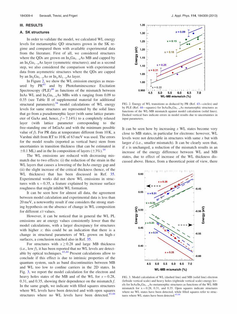
calculation and experimental data is quite good. For struc-
tures of case (i), the reported experimental WL energy level
for structures with x¼ 0.16, y¼ 0.30 was 1.088 eV (Ref. 36)
and present calculation give a WL level at 1.090 eV;
for x¼ 0.20, y¼ 0.40, the experimental data was 1.123 eV
(Ref. 37) against a 1.110 eV calculated value; and for
x¼ 0.25, y¼ 0.45, the experimental data was 1.077 eV
(Ref. 37) while the model calculated value was 1.070 eV. In
case (ii) for x¼ 0.15 and y¼ 0.20 and 0.10, the experimental
WL energy was 1.340 eV and a 1.355 eV, respectively,43
comparing with model values of 1.345 eV and 1.350 eV.
These results confirm that the model can help predict meta-
morphic 2D states also for more complex structure design.
Incidentally, we note that structures with InAlAs layers
are a good example of the usefulness of this model to control
the quantum energy system by an adroit design engineering
of the metamorphic structure: from these results, it is proven
that it is possible to raise WL levels above InxGa1�xAs MB
energy states by using InAlAs embedding layers below and
above QDs, with interesting consequences for QD carrier
dynamics.
FIG. 4. Energy of WL transitions as
deduced by PL (Ref. 25)—full circles)
against model calculation (open
squares) as functions of x. Values of y
of upper layers (Ref. 25) are indicated.
Inset: 10 K PL spectra for structures
with x¼ 0.22 and x¼ 0.22 (red),
y¼ 0.30 (blue). The WL value calcu-
lated by the model is indicated by
dashed lines.
FIG. 5. Model calculation of WL energy (continuous line) and experimental
QD peak emission (open squares) as deduced by PL (Ref. 25) in sub-critical
structures as functions of x. Vertical bars indicate FWHM values of QD
emission. Dashed line is a guide for the eye.
184309-5 Seravalli, Trevisi, and Frigeri J. Appl. Phys. 114, 184309 (2013)
B. Sub-critical coverages structures
The interest in these structures relies in the very low den-
sity of QDs that is attainable, making them attractive for the
development of single photon sources in the 1.3–1.55 lm
range. From this perspective, the properties of WL levels and
their dependence on MB parameters are of great interest due
to the fact that, beside effect on the thermal properties of QD
emission, WL-confined carriers levels are known to influence
single photon characteristics via Coulomb interaction.21
In Figure 4, we present comparison of model calcula-
tion of WL states and experimental PL emission of WL lev-
els as functions of the MB composition x for structures
where the MB thickness was fixed to 500 nm (hence with
fixed MB-QD mismatch for same x), while InyGa1�yAs
capping layers with y> x were used to further red-shift the
QD emission.25 Due to the low density of QDs, standard PL
characterization allows to detect light emission also from
WL states, in contrast with SK structures. The agreement
between model calculation and PL peaks is always less than
15 meV (except for the x¼ 0.15 y¼ 0.45 case). Data are
taken from Ref. 25 and from unpublished data for x¼ 0.15,
y> x (see supplemental material for experimental details
and for structural parameters).34 For x¼ 0.30, no emission
has been reported from WL, similarly to SK structures,
although the model predicts to have WL levels at the
1.030 eV for x¼ y¼ 0.30 at about 70 meV from QD peak
emission. Previous indications of effect of high-x, high-tsurfaces on WL formation that have been discussed in
depth in the previous sections are confirmed also for struc-
tures deposited by sub-critical coverages.
From the comparison of WL levels calculation and PL
experimental data, it can be concluded that the model is vali-
dated also for structures with a low density of QDs (with dis-
crepancies in the range of 15 meV) and it could be used for
advanced metamorphic structure design, for example, to
engineer 2D carrier energy and localization.
As a very interesting case of study, let us consider struc-
tures with x¼ 0.22 (whose PL spectra are shown in the inset
of Fig. 4), where the expected WL emission falls in the tail
of the large QD emission (in low density structures, QD pres-
ent very wide emission due to higher dishomogeneities of
QD size and/or compositions). This suggests that it could be
possible to have small energy difference between energy lev-
els for carriers confined in some isolated QDs (emitting in
the high-energy tail) and 2D WL levels: this could result in
an increase of the electronic coupling between single elec-
trons in QDs and the 2D electron gas in the WL, up to a pos-
sible establishment of an hybrid 0D-2D system, a topic of
great recent interest.46–48
In order to make some more general assessment on this
possibility, let us consider, in Fig. 5, the PL emission of WL
and of sub-critical QDs25 presented as functions of x. It can
be noticed how the energy difference between QD and WL
emission reduces with the increase of the MB In composi-
tion. This dependence allows to predict that in the high-xranges (x� 0.25), the WL emission energy difference with
QDs could become less than the full width half maxima
(FWHM) of the QD PL spectrum (indicated in Figure 5 as a
vertical bar of about 100 meV): this means that a good frac-
tion of isolated QDs could be in resonance with WL levels.
However, it should be kept in mind that there is the limita-
tion on x related to the absence of WL states discussed
above: for this reason, an hybrid 0D-2D systems composed
by an isolated QD and the WL could be realized for values
of x ranging from 0.20 to 0.30. As a second example of the
usefulness of this model to predict properties of metamor-
phic 2-dimensional quantum system, let us consider the spa-
tial localization of carriers confined in the WL.
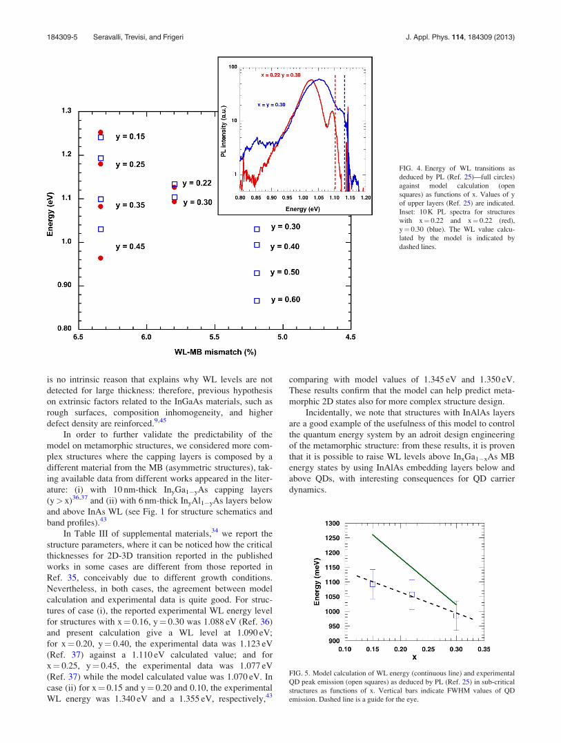
In Fig. 6, we show the band profiles and the squared val-
ues of the wavefunctions of carriers for the metamorphic sys-
tem with x¼ 0.15, using capping layers going from y¼ 0.15
to 0.35, for structures grown by the deposition of subcritical
FIG. 6. Plots along growth direction of: VB profile (thicker blue line), CB profile (thicker red line), ground electron (red line) and heavy hole (blue line) energy
levels, first electron (dashed red line), and heavy hole (dashed blue line) excited levels (leftside vertical scale) calculated by the model. Plots along growth
direction of model calculations of squared absolute values of electron (blue line) and heavy hole (red line) wavefunctions (right handside).
184309-6 Seravalli, Trevisi, and Frigeri J. Appl. Phys. 114, 184309 (2013)

InAs coverages. In the case of x¼ 0.25 and 0.35, a mixed
WL-QW system emerges, where the spatial localization of
carriers may greatly differ. This is a system that has been
explored recently, as a possible mean to control the Coulomb
interaction between QD and WL carriers via their spatial
separation.27
When y¼ 0.15, carriers in the ground levels are confined
within the WL; while in the y¼ 0.25 case, the electron
spreads into the cap layer and the heavy hole has still a
greater probability of being in the WL than in the InGaAs
capping layer. When y¼ 0.35, the situation is totally differ-
ent as both carriers are delocalized in the upper layer and the
WL does not seem to have any effect in confining them. This
is a very interesting result, as it has been very recently exper-
imentally proved that heavy holes cannot be completely
delocalized from the WL in pseudomorphic InAs/InGaAs
QD structures.38
In Fig. 7, we present the overlap integral of the heavy
hole-electron wavefunctions for the ground states in the WL
and the carrier probability of being found in the WL as func-
tions of y in the whole range 0� y� 0.35 (x value remains
constant at 0.15).
It is interesting to notice that while electrons are weakly
localized within the WL even for y¼ 0.15 and spread in the
capping layer (for y> x) or in the MB (for y< x), heavy
holes become completely delocalized from the WL only
when y¼ 0.35, effectively spatially separating the 2D system
from the 0D QD system. Also the overlap integral (propor-
tional to the radiative recombination probability) changes
consistently, reducing by almost the half when y¼ 0 (due to
the delocalization of electrons) and by much less when
y¼ 0.35 (due to the concomitant delocalization of electron
and heavy holes from the WL to the InGaAs capping layer).
The different dependence of 2D carrier localization on the
structure design suggests the possibility to engineer the inter-
action between QD and WL carriers, also by selecting nega-
tive or positive 2D charge carriers to electrically interact
with QD carriers. This is a very interesting example of how
the metamorphic system is a flexible system, with a wider
degree of engineering possibilities with respect to the
pseudomorphic system, for advanced design of structures for
single photon sources. As showed above, these possibilities
include: (i) engineering of WL carrier spatial localization in
structures for single photon emission, to reduce the Coulomb
interactions with QD confined carriers, (ii) separation of
electrons and heavy holes in the 2D WL system, thus reduc-
ing the radiative recombination processes and influencing
the QD carrier dynamics, and (iii) find conditions for strong
electronic coupling between QD-WL states of great interest
for single photon devices. In structures where carriers are
electrically driven into QDs, the 0D–2D system could be
switched on/off by simple application of external bias.
Hence, from these results, it can be concluded that the meta-
morphic QD system is not only a viable approach to obtain
single photon emission in the 1.3–1.55 lm range, but can
provide useful tools to control electronic interactions
between 0D and 2D carriers.
IV. CONCLUSIONS
In conclusion, we developed a simple model for the
calculation of quantum 2D states in metamorphic buffers
and applied it to the case of InAs WL in metamorphic
InAs/InGaAs QD nanostructures. The model was validated
against experimental data from different research groups,
for structures grown in the Stranski-Krastanow regime and
with sub-critical coverages. The analysis of model results
highlighted the unique properties of metamorphic system of
having two independent design parameters, namely the MB
thickness and composition that determine the MB-WL mis-
match. The effect of the change of mismatch and of MB
composition on WL properties was considered, allowing to
reach interesting conclusions.
It was confirmed that the previously reported WL disap-
pearance in InAs/InGaAs system for high x/high t is an
extrinsic effect, probably related to the surface roughness on
which InAs is deposited.
For structures with a low density of QDs, the effect of the
change in composition of the capping layer on the spatial deloc-
alization of 2D carriers (that influence the Coulomb interaction
between QD and WL carriers) and on the electron-heavy hole
spatial separation in the QW-WL system (that determines the
probability of radiative recombination) was studied and allowed
to draw interesting conclusions. In metamorphic InAs/InGaAs
system, it could be possible to expel both carriers from the WL,
a feature not obtainable in pseudomorphic GaAs-based struc-
tures, where only the electron can be delocalized from the WL.
Moreover, model calculations suggest that in these systems, it
could be possible to have QD and WL levels resonate in energy
(at least for a fraction of the QD ensemble). On the basis of
these model results, it seems viable to propose the use of meta-
morphic InAs/InGaAs QDs as: (i) a possible system to have
hybrid 2D–0D quantum levels and (ii) a scheme for QD-based
single photon sources where the interaction between WL and
QD carrier can be engineered. More in general, one could think
at the metamorphic approach as a system that allows to engi-
neer two properties of the QW system: this could be a feature
not limited to QD structures, but it could also have applications
in other metamorphic 2-dimensional structures (QW lasers,
FIG. 7. (Left handside) Overlap of ground electron and heavy hole wave-
functions in WL-QW levels as function of y from model calculations
(crosses). (Right handside) Probability of finding a carrier within 1 nm of the
WL as functions of y from model calculations for heavy holes (circles) and
electrons (squares). Lines are guides for the eye.
184309-7 Seravalli, Trevisi, and Frigeri J. Appl. Phys. 114, 184309 (2013)
high mobility devices, such as MHEMT, semiconductor optical
amplifiers, and QW solar cells).
1W. Guter, J. Schoene, S. P. Philipps, M. Steiner, G. Siefer, A. Wekkeli, E.
Welser, E. Oliva, A. W. Bett, and F. Dimroth, Appl. Phys. Lett. 94,
223504 (2009).2J. S. Gandhi, C. U. Kim, and W. P. Kirk, in Conference Record of theIEEE Photovoltaic Specialists Conference (2012), p. 789.
3I. Tangring, H. Ni, B. P. Wu, D. H. Wu, Y. Xiong, S. Huang, Z. Niu, S. M.
Wang, Z. H. Lai, and A. Larsson, Appl. Phys. Lett. 91, 221101 (2007).4Y. Xin, L. Vaughn, L. R. Dawson, A. Stintz, Y. Lin, L. F. Lester, and
D. L. Huffaker, J. Appl. Phys. 94, 2133 (2003).5S.-G. Ihn, S. J. Jo, and J.-I. Song, Appl. Phys. Lett. 88, 132108 (2006).6J. A. Czaban and D. A. Thompson, Nanotechnology 21, 134005 (2010).7C. P. Jiang, Z. M. Huang, S. L. Guo, J. H. Chu, L. J. Cui, Y. P. Zeng, Z. P.
Zhu, and B. Q. Wang, Appl. Phys. Lett. 79, 1909 (2001).8M. Boudrissa, E. Delos, C. Gaquiere, M. Rousseau, Y. Cordiere, D. Theron,
and J. C. De Jaeger, IEEE Trans. Electron Devices 48, 1037 (2001).9L. Seravalli, P. Frigeri, L. Nasi, G. Trevisi, and C. Bocchi, J. Appl. Phys.
108, 064324 (2010).10G. Balakrishnan, S. Huang, T. J. Rotter, A. Stintz, L. R. Dawson, K. J.
Malloy, H. Xu, and D. L. Huffaker, Appl. Phys. Lett. 84, 2058 (2004).11Z. Mi and P. Bhattacharya, J. Appl. Phys. 98, 023510 (2005).12L. Seravalli, P. Frigeri, G. Trevisi, and S. Franchi, Appl. Phys. Lett. 92,
213104 (2008).13L. Seravalli, M. Minelli, P. Frigeri, S. Franchi, G. Guizzetti, M. Patrini, T.
Ciabattoni, and M. Geddo, J. Appl. Phys. 101, 024313 (2007).14L. Seravalli, P. Frigeri, M. Minelli, P. Allegri, V. Avanzini, and S.
Franchi, Appl. Phys. Lett. 87, 063101 (2005).15M. Hugues, M. Teisseire, J.-M. Chauveau, B. Vinter, B. Damilano, J.-Y.
Duboz, and J. Massies, Phys. Rev. B 76, 075335 (2007).16C. Cornet, C. Platz, P. Caroff, J. Even, C. Labb�e, H. Folliot, A. Le Corre,
and S. Loualiche, Phys. Rev. B 72, 35342 (2005).17S. Lee, O. L. Lazarenkova, P. von Allmen, F. Oyafuso, and G. Klimeck,
Phys. Rev. B 70, 125307 (2004).18S. Sanguinetti, D. Colombo, M. Guzzi, E. Grilli, M. Gurioli, L. Seravalli,
P. Frigeri, and S. Franchi, Phys. Rev. B 74, 205302 (2006).19G. Gelinas, A. Lanacer, R. Leonelli, R. A. Masut, and P. J. Poole, Phys.
Rev. B 81, 235426 (2010).20M. Winger, T. Volz, G. Tarel, S. Portolan, A. Badolato, K. J. Hennessy, E.
L. Hu, A. Beveratos, J. Finley, V. Savona, and A. Imamoglu, Phys. Rev.
Lett. 103, 207403 (2009).21N. Chauvin, C. Zinoni, M. Francardi, A. Gerardino, L. Balet, B. Alloing,
L. H. Li, and A. Fiore, Phys. Rev. B 80, 241306 (2009).22Y. Chen and J. Washburn, Phys. Rev. Lett. 77, 4046 (1996).23G. SeRk, K. Ryczko, M. Motyka, J. Andrzejewski, K. Wysocka, J. Misiewicz,
L. Li, A. Fiore, and G. Patriarche, J. Appl. Phys. 101, 063539 (2007).24H. Song, T. Usuki, Y. Nakata, N. Yokoyama, H. Sasakura, and S. Muto,
Phys. Rev. B 73, 115327 (2006).25L. Seravalli, G. Trevisi, and P. Frigeri, Cryst. Eng. Commun. 14, 6833 (2012).26See www.tibercad.org for TiberLab.
27L. Seravalli, C. Bocchi, G. Trevisi, and P. Frigeri, J. Appl. Phys. 108,
114313 (2010).28P. Maree, J. Barbour, J. Vanderveen, K. Kavanagh, C. Bullelieuwma, and
M. Viegers, J. Appl. Phys. 62, 4413 (1987).29M. Geddo, G. Guizzetti, M. Patrini, T. Ciabattoni, L. Seravalli, P. Frigeri,
and S. Franchi, Appl. Phys. Lett. 87, 263120 (2005).30V. Bellani, C. Bocchi, T. Ciabattoni, S. Franchi, P. Frigeri, P. Galinetto,
M. Geddo, F. Germini, G. Guizzetti, L. Nasi, M. Patrini, L. Seravalli, and
G. Trevisi, Eur. Phys. J. B 56, 217 (2007).31F. Pollak and M. Cardona, Phys. Rev. 172, 816 (1968).32P. Wang, N. Ledentsov, C. Sotomayor Torres, I. Yassievich, A.
Pakhomov, A. Egovov, P. Kop’ev, and V. M. Ustinov, Phys. Rev. B 50,
1604 (1994).33I. Vurgaftman, J. Meyer, and L. Ram-Mohan, J. Appl. Phys. 89, 5815
(2001).34See supplemental material at http://dx.doi.org/10.1063/1.4830021 for ma-
terial parameters and experimental details.35L. Seravalli, G. Trevisi, and P. Frigeri, Cryst. Eng. Commun. 14, 1155
(2012).36E. Y. Lin, C. Y. Chen, T. E. Tzeng, S. L. Chen, D. J. Y. Feng, and T. S.
Lay, Physica E 42, 2544 (2010).37N. V. Kryzhanovskaya, A. Y. Gladyschev, S. Blokhin, Y. G. Musikhin,
A. E. Zhukov, M. V. Maksimov, N. Zakharov, A. Tsatsul’nikov, N. N.
Ledentsov, P. Werner, F. Guffarth, and D. Bimberg, Semiconductors 38,
833 (2004).38L. Seravalli, G. Trevisi, P. Frigeri, F. Rossi, E. Buffagni, and C. Ferrari,
J. Phys. D: Appl. Phys. 46, 315101 (2013).39J. Ib�a~nez, R. Cusc�o, S. Hern�andez, L. Art�us, M. Henini, A. Patane, L.
Eaves, M. Roy, and P. A. Maksym, J. Appl. Phys. 99, 043501 (2006).40C. Heyn, A. Bolz, T. Maltezopoulos, R. Johnson, and W. Hansen, J. Cryst.
Growth 278, 46 (2005).41D. Litvinov, D. Gerthsen, A. Rosenauer, M. Schowalter, T. Passow, P.
Fein€augle, and M. Hetterich, Phys. Rev. B 74, 165306 (2006).42R. R. Pel�a, L. K. Teles, M. Marques, and S. Martini, J. Appl. Phys. 113,
033515 (2013).43L. Seravalli, G. Trevisi, P. Frigeri, S. Franchi, M. Geddo, and G. Guizzetti,
Nanotechnology 20, 275703 (2009).44L. Seravalli, G. Trevisi, P. Frigeri, R. J. Royce, and D. J. Mowbray,
J. Appl. Phys. 112, 034309 (2012).45E. S. Semenova, A. E. Zhukov, S. Mikhrin, A. Y. Egorov, V. A.
Odnoblyudov, A. P. Vasil Ev, E. V. Nikitina, A. R. Kovsh, N. V.
Kryzhanovskaya, A. Y. Gladyschev, S. A. Blokhin, Y. G. Musikhin, M. V.
Maksimov, Y. M. Shernyakov, V. M. Ustinov, and N. N. Ledentsov,
Nanotechnology 15, S283 (2004).46Y. I. Mazur, V. G. Dorogan, M. E. Ware, E. Marega, Jr., M. Benamara,
Z. Y. Zhuchenko, G. G. Tarasov, C. Lienau, and G. J. Salamo, Nanoscale
4, 7509 (2012).47V. G. Dorogan, Y. I. Mazur, E. Marega, G. G. Tarasov, M. E. Ware, and
G. J. Salamo, J. Appl. Phys. 105, 124304 (2009).48M. Syperek, J. Andrzejewski, W. Rudno-Rudzi�nski, G. SeRk, J. Misiewicz,
E.-M. Pavelescu, C. Gilfert, and J. P. Reithmaier, Phys. Rev. B 85, 125311
(2012).
184309-8 Seravalli, Trevisi, and Frigeri J. Appl. Phys. 114, 184309 (2013)