Positive Bias Instability and Recovery in InGaAs Channel nMOSFETs
Upload
khangminh22Category
view
1download
0


Karl Schneider
Broadband Amplifiers for High Data Rates using InP/InGaAs Double Heterojunction Bipolar Transistors


Broadband Amplifiers for High Data Rates using InP/InGaAs DoubleHeterojunction Bipolar Transistors
von Karl Schneider

Universitätsverlag Karlsruhe 2006 Print on Demand
ISBN 3-86644-021-9
Impressum
Universitätsverlag Karlsruhec/o UniversitätsbibliothekStraße am Forum 2D-76131 Karlsruhewww.uvka.de
Dieses Werk ist unter folgender Creative Commons-Lizenz lizenziert: http://creativecommons.org/licenses/by-nc-nd/2.0/de/
Dissertation, Universität Karlsruhe (TH)Fakultät für Elektrotechnik und Informationstechnik, 2006


Broadband Amplifiers for High Data Rates usingInP/InGaAs Double Heterojunction Bipolar
Transistors
Zur Erlangung des akademischen Grades eines
DOKTOR-INGENIEURS
von der Fakultat fur
Elektrotechnik und Informationstechnik
der Universitat Fridericiana Karlsruhe
genehmigte
DISSERTATION
von
Dipl.-Ing. Karl Schneider
aus Hannover
Tag der mundlichen Prufung: 16. Januar 2006Hauptreferent: Prof. Dr. rer. nat. G. WeimannKorreferent: Prof. Dr.-Ing. W. Wiesbeck


Contents
Kurzfassung 1
Abstract 2
1 Introduction 31.1 Motivation . . . . . . . . . . . . . . . . . . . . . . . . . . . . . . . . . . . . 3
1.1.1 Scope of the Work . . . . . . . . . . . . . . . . . . . . . . . . . . . 51.2 State of the Art . . . . . . . . . . . . . . . . . . . . . . . . . . . . . . . . . 6
1.2.1 Broadband Amplifiers . . . . . . . . . . . . . . . . . . . . . . . . . 61.2.2 Devices . . . . . . . . . . . . . . . . . . . . . . . . . . . . . . . . . 7
2 InP-based Double Heterojunction Bipolar Transistor 112.1 Operating Principle . . . . . . . . . . . . . . . . . . . . . . . . . . . . . . . 122.2 Technology . . . . . . . . . . . . . . . . . . . . . . . . . . . . . . . . . . . 16
2.2.1 Active Devices . . . . . . . . . . . . . . . . . . . . . . . . . . . . . 162.2.2 Passive Structures . . . . . . . . . . . . . . . . . . . . . . . . . . . 18
2.3 Layer Structure Optimization . . . . . . . . . . . . . . . . . . . . . . . . . 192.3.1 Initial Layer Structure (A) . . . . . . . . . . . . . . . . . . . . . . . 192.3.2 Improved Layer Structure (B) . . . . . . . . . . . . . . . . . . . . . 242.3.3 Optimized Layer Structure (C) . . . . . . . . . . . . . . . . . . . . 282.3.4 Summary . . . . . . . . . . . . . . . . . . . . . . . . . . . . . . . . 33
2.4 Transistor Layout Optimization . . . . . . . . . . . . . . . . . . . . . . . . 342.4.1 Emitter Width Design . . . . . . . . . . . . . . . . . . . . . . . . . 362.4.2 Base Contact Width Design . . . . . . . . . . . . . . . . . . . . . . 382.4.3 Collector Contact Design . . . . . . . . . . . . . . . . . . . . . . . . 402.4.4 Emitter Length Design . . . . . . . . . . . . . . . . . . . . . . . . . 402.4.5 Summary . . . . . . . . . . . . . . . . . . . . . . . . . . . . . . . . 43
3 Transistor Models 453.1 Large-Signal Models . . . . . . . . . . . . . . . . . . . . . . . . . . . . . . 46
3.1.1 Gummel-Poon Model . . . . . . . . . . . . . . . . . . . . . . . . . . 463.1.2 Alternative Models . . . . . . . . . . . . . . . . . . . . . . . . . . . 473.1.3 UCSD Model . . . . . . . . . . . . . . . . . . . . . . . . . . . . . . 47
III

IV Contents
3.2 UCSD Model Extraction . . . . . . . . . . . . . . . . . . . . . . . . . . . . 493.2.1 Diode Parameters . . . . . . . . . . . . . . . . . . . . . . . . . . . . 493.2.2 Resistances . . . . . . . . . . . . . . . . . . . . . . . . . . . . . . . 513.2.3 Junction Capacitances . . . . . . . . . . . . . . . . . . . . . . . . . 553.2.4 Transit and Delay Times . . . . . . . . . . . . . . . . . . . . . . . . 56
3.3 Small-Signal Model . . . . . . . . . . . . . . . . . . . . . . . . . . . . . . . 603.3.1 Model Extraction . . . . . . . . . . . . . . . . . . . . . . . . . . . . 603.3.2 Investigation of Transistors . . . . . . . . . . . . . . . . . . . . . . . 63
3.4 Summary . . . . . . . . . . . . . . . . . . . . . . . . . . . . . . . . . . . . 68
4 Methods of Broadband Amplifier Characterization 694.1 Figures of Merit . . . . . . . . . . . . . . . . . . . . . . . . . . . . . . . . . 69
4.1.1 Bandwidth . . . . . . . . . . . . . . . . . . . . . . . . . . . . . . . . 694.1.2 Group Delay . . . . . . . . . . . . . . . . . . . . . . . . . . . . . . . 714.1.3 Output Power . . . . . . . . . . . . . . . . . . . . . . . . . . . . . . 71
4.2 Small-Signal-Characterization (S-Parameter) . . . . . . . . . . . . . . . . . 724.3 Large-Signal-Characterization . . . . . . . . . . . . . . . . . . . . . . . . . 73
4.3.1 Output Power . . . . . . . . . . . . . . . . . . . . . . . . . . . . . . 734.3.2 Signal Distortion (Eye-Diagram) . . . . . . . . . . . . . . . . . . . . 74
5 Realization of Compact Lumped Amplifiers 775.1 Design Considerations . . . . . . . . . . . . . . . . . . . . . . . . . . . . . 775.2 Realized Amplifiers . . . . . . . . . . . . . . . . . . . . . . . . . . . . . . . 79
5.2.1 Comparison of Lumped Amplifier Approaches . . . . . . . . . . . . 795.2.2 High-Gain Amplifier for 40 Gbit/s . . . . . . . . . . . . . . . . . . . 825.2.3 Low-Power Amplifier for 80 Gbit/s . . . . . . . . . . . . . . . . . . 85
5.3 Output Power Limit . . . . . . . . . . . . . . . . . . . . . . . . . . . . . . 87
6 Distributed Amplifiers for 80 Gbit/s 916.1 Design Considerations . . . . . . . . . . . . . . . . . . . . . . . . . . . . . 92
6.1.1 Gain Cell Design Concepts . . . . . . . . . . . . . . . . . . . . . . . 936.1.2 Attenuation Compensation . . . . . . . . . . . . . . . . . . . . . . . 936.1.3 Coplanar and Microstrip Transmission Lines . . . . . . . . . . . . . 966.1.4 Transmission Line Termination . . . . . . . . . . . . . . . . . . . . 976.1.5 Linear and Matrix Design . . . . . . . . . . . . . . . . . . . . . . . 986.1.6 Single-ended and Differential Design . . . . . . . . . . . . . . . . . 98
6.2 Realized Amplifiers . . . . . . . . . . . . . . . . . . . . . . . . . . . . . . . 996.2.1 Low-Power 100 GHz Bandwidth Amplifier . . . . . . . . . . . . . . 996.2.2 Tunable Amplifier for Loss Compensation . . . . . . . . . . . . . . 1036.2.3 High-Power Amplifier for 80 Gbit/s . . . . . . . . . . . . . . . . . . 108
6.3 Summary . . . . . . . . . . . . . . . . . . . . . . . . . . . . . . . . . . . . 114
7 Conclusion and Outlook 115

Contents V
A Extracted Large-Signal Model Parameters 117
Bibliography 119
List of Abbreviations 129
Acknowledgments 131
Curriculum Vitae 132

VI Contents

Kurzfassung
Diese Arbeit beschreibt die Entwicklung von elektrischen Breitbandverstarkern, die furden Einsatz als Modulatortreiber in optischen Nachrichtenubertragungssystemen, die beieiner Datenrate von 80 Gbit/s arbeiten, geeignet sind. Diese Systeme ermoglichen dieDatenubertragung bei sehr hohen Bitraten, die die Anforderungen der stetig wachsendenInformationstechnologien, zu denen der Mobilfunk und das Internet gehoren, erfullen kon-nen. Die Realisierung der Verstarker wird in einem dreistufigen Entwicklungsprozess er-reicht.
Als erstes werden die geometrischen Dimensionen, d.h. die vertikale Schichtstrukturund die lateralen Abmessungen der Einzeltransistoren der verwendeten InP-basierten Dop-pel-Hetero-Bipolartransistortechnologie optimiert. Dieses ist ein wichtiger Beitrag zur Ent-wicklung einer Transistortechnologie, die eine Kombination von sehr hoher Geschwindigkeitund hoher Durchbruchspannung bietet, die fur die Herstellung von Modulatortreibern fur80 Gbit/s erforderlich ist und die von Silizium-basierten Technologien nicht geleistet wer-den kann. Experimentelle Untersuchungen verschiedener Transistoren zeigen, dass dievertikalen und laterale Abmessungen entscheidenden Einfluss auf das Transistorverhaltenhaben. Nach drei Iterationen haben die Transistoren eine Gute erreicht, die die Entwik-klung von integrierten Schaltungen fur 80 Gbit/s erlaubt.
Im zweiten Entwicklungsschritt werden geeignete Transistormodelle bereitgestellt. Ausmehreren publizierten Modellierungsansatzen, wird der aussichtsreichste ubernommen undfur die beabsichtigte Anwendung optimiert. Die Gultigkeit der Modelle wird durch denVergleich von Messung und Simulation einzelner Transistoren und komplexer Schaltungenverifiziert. Die erzeugten Modelle sind nicht nur fur die Groß- und Kleinsignalsimulationvon analogen Schaltungen, sondern auch fur die Entwicklung der digitalen Schaltungeneines Nachrichtenubertragungssystems geeignet.
Schließlich werden mit Hilfe der optimierten Transistoren und Modelle verschiedeneVerstarker auf Grundlage unterschiedlicher Konzepte entworfen, hergestellt und mit S-Parameter-, Leistungs- und Augendiagrammmessungen untersucht. Die konzentriertenVerstarker weisen Vorteile wie geringe Leistungsaufnahme, kleine Abmessungen und damitgeringe Herstellungskosten auf. Ihre Ausgangsleistung ist jedoch sehr begrenzt. Im Gegen-satz dazu bieten die verteilten Verstarker mehr Ausgangsleistung und hohere Bandbreite.Ein auf Leistung optimierter verteilter Verstarker erweist sich als besonders geeignet furdie Entwicklung von Modulatortreibern fur 80 Gbit/s und gehort zu besten Ergebnissen,die in diesem Bereich bisher veroffentlicht wurden.
1

Abstract
This work describes the development process of electrical broadband amplifiers, whichare suitable as modulator drivers in electrical time division multiplex (ETDM) systems,operating at 80 Gbit/s. Such systems are promising candidates for the next generation ofhigh bit rate data transmission systems, which can satisfy the demands of the continuouslygrowing information technologies, including mobile communications and internet. Therealization is accomplished in three major development steps.
First, the vertical dimensions, i.e. the epitaxial layer structure, as well as the lateraldimensions, i.e. the transistor layout, of InP-based Double Heterojunction Bipolar Tran-sistors (DHBT) are optimized. This is an important contribution in the development of anInP-technology, which offers devices with a combination of high speed and breakdown volt-age, suitable for modulator driver development at 80 Gbit/s and not achievable with siliconbased technologies. Various direct current (DC) and high frequency (HF) measurements ofdifferent DHBTs are conducted and the results are related to the devices’ geometries. It isshown, that optimized vertical and horizontal dimensions are crucial for realizing high per-formance transistors. The optimized devices feature state-of-the-art performance allowingthe development of integrated circuits for 80 Gbit/s.
Second, transistor models are obtained from extracted device data. From several pub-lished models, the most suitable approach is adopted and subsequently refined and op-timized to make a compromise between accuracy and complexity. The validity of thesemodels is confirmed by comparing not only measurement and simulation results of tran-sistors, but also of complex circuits. In addition, these models are not only used forsmall-signal and large-signal simulations in analog circuits, but are equally suitable fordeveloping digital circuits of an ETDM system.
Third, using the optimized transistors and models, several amplifiers representing dif-ferent design concepts are realized and experimentally evaluated using S-parameter, powerand eye diagram measurements. Lumped amplifiers show a low power consumption at80 Gbit/s operation. An additional advantage is their small chip size and subsequent lowcosts. However, their output power capabilities are very limited. In contrast, distributedamplifiers are more complex, but offer extended bandwidth and superior output powerlevels. A state-of-the-art distributed amplifier featuring eight gain cells, each using emitterfollowers and a cascode configuration at its input and output, respectively, shows superiorperformance with respect to modulator driver application at 80 Gbit/s. These results are asignificant contribution towards the realization of ETDM systems operating at 80 Gbit/s.
2

Chapter 1
Introduction
1.1 Motivation
By the end of the 20th century and the beginning of the 21st century the telecommuni-cation and information technology started to change society strongly. Today, all areas ofsociety, politics, and economy make use of the possibilities of these technologies and asa consequence the influence on economic processes, for example, is enormous. Also theprivate user takes more and more advantage of the possibilities of mobile communicationand internet. Consequently, the requirements on the telecommunication technologies havechanged dramatically, as they have come to play a key role in all social areas and in the
MUXD2
D1
D2DE
MU
Xlaser diode
modulator driver
multiplexer demultiplexer
clock & datarecovery
photodiode
optical fiber
transimpedanceamplifier
modulator
D1
CLK CLK
MD CDR
Figure 1.1: Schematic of ETDM system. Two data channels (D1, D2) are multiplexed into asingle data stream and transmitted over an optical fiber. At the receiver side the data channelsD1 and D2 are recovered.
3
4 1. Introduction
Modulator Driver
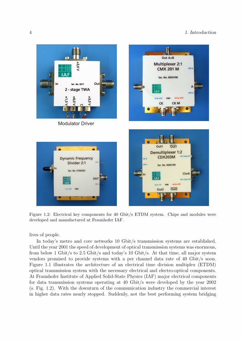
Figure 1.2: Electrical key components for 40 Gbit/s ETDM system. Chips and modules weredeveloped and manufactured at Fraunhofer IAF.
lives of people.
In today’s metro and core networks 10 Gbit/s transmission systems are established.Until the year 2001 the speed of development of optical transmission systems was enormous,from below 1 Gbit/s to 2.5 Gbit/s and today’s 10 Gbit/s. At that time, all major systemvendors promised to provide systems with a per channel data rate of 40 Gbit/s soon.Figure 1.1 illustrates the architecture of an electrical time division multiplex (ETDM)optical transmission system with the necessary electrical and electro-optical components.At Fraunhofer Institute of Applied Solid-State Physics (IAF) major electrical componentsfor data transmission systems operating at 40 Gbit/s were developed by the year 2002(s. Fig. 1.2). With the downturn of the communication industry the commercial interestin higher data rates nearly stopped. Suddenly, not the best performing system bridging

1.1. Motivation 5
a distance of several thousands of kilometers was of interest, but a cheap system justsatisfying the short-term requirements.
Recently, the situation has become more relaxed again. Some operators now ask for theoption to deploy 40 Gbit/s systems, although so far no larger installation of this bit ratehas been performed. To be prepared for the next step, the development of optical datatransmission systems at even higher bit rates was started. In 2002 as part of the effort,Fraunhofer IAF undertook the task of developing all electrical components needed for an80 Gbit/s ETDM optical data link.
1.1.1 Scope of the Work
The scope of this thesis is the development of broadband amplifiers suitable as trans-impedance amplifiers and modulator drivers in ETDM systems with a data rate of 80 Gbit/sand beyond (Fig. 1.1). This task required not only the design of the electrical circuits, but agreat amount of preliminary development steps, which are a prerequisite for circuit design.The necessary work packages, that were solved in the course of this work, are described inthe following paragraphs.
First of all a new InP-based heterojunction bipolar transistor (HBT) technology hadto be developed at Fraunhofer IAF, which provided transistor devices with excellent high-frequency performance and high breakdown voltages. Although Fraunhofer IAF has a longtradition of providing state-of-the-art technologies, the existing technologies did either notprovide enough breakdown voltage or speed with respect to modulator driver development.This work contributed an experimental investigation and evaluation of different epitaxiallayer structures. Furthermore, the high-frequency performance of transistors dependingon device geometry was measured and evaluated. The efforts resulted in high-performancetransistor devices with optimized vertical and lateral dimensions in the new technology.The optimization process is described in Chapter 2.
The link between technology, i.e., the single physical devices, and the design of complexcircuits is a transistor model. From several proposed InP-HBT models, the most promis-ing model approach was adopted. Starting from a rudimentary extraction procedure, theextraction of the model was refined and optimized to make a compromise between com-plexity and accuracy. This resulted in transistor models, which were successfully appliedin the design of circuits. Furthermore, models were used to provide an insight into severaltransistors revealing limitations of the devices. This knowledge supported the optimizationof the devices (Chapter 2). The underlying model considerations, the extraction procedureand modeling results are presented in Chapter 3.
Before circuits can be successfully designed, figures of merit (FOMs) and requirementshave to be defined. In addition, measurement procedures have to be determined, whichallow to evaluate the amplifiers with respect to the FOMs. Chapter 4 summarizes the keyrequirements for amplifiers used at bit rates of 80 Gbit/s and beyond and gives an overviewof the measurement techniques that were used to test the amplifiers.
With optimized transistor devices and suitable models at hand, the development ofamplifiers according to the requirements is possible. For amplifiers two common design

6 1. Introduction
approaches exist: the lumped amplifier and the distributed amplifier. For both approachesseveral concepts were realized, evaluated and optimized with respect to different designgoals like bandwidth, output power or both. The most challenging part was the realizationof an amplifier concept, which features enough bandwidth as well as enough output powerfor the realization of modulator drivers. The results of the design efforts are described inChapter 5 for lumped amplifiers and in Chapter 6 for distributed amplifiers.
Relationship to other Work at Fraunhofer IAF
As stated above, the development efforts at Fraunhofer IAF are aiming towards the real-ization of not only amplifiers but all electrical components needed for an ETDM systemoperating at 80 Gbit/s (s. Fig. 1.1). Consequently, some results of this thesis contributedto the realization of other system components as well. The optimized transistor devices(Chapter 2) were the building blocks not only in analog amplifier, but also in digital circuitdesign. The transistor model extraction (Chapter 3) was optimized for the simulation ofanalog as well as digital circuits. Among these related circuits are a 80 Gbit/s 2:1 mul-tiplexer (MUX) [74], a low phase noise voltage controlled oscillator (VCO) operating upto 89 GHz [73], as well as a 80 Gbit/s clock and data recovery circuit (CDR) with a 1:2demultiplexer [72]. In summary, the combined efforts at IAF have provided a transistortechnology and all circuit concepts needed for an 80 Gbit/s ETDM system in a period ofless than four years.
1.2 State of the Art
1.2.1 Broadband Amplifiers
Bandwidth
High-speed optical data communication systems require broadband amplifier circuits withhigh gain. Distributed amplifiers (DA) are ideal candidates for enhancing bandwidth,because the input and output artificial transmission lines have high cut-off frequencies.Using high electron mobility transistors (HEMT), excellent circuit performance with band-width values exceeding 110 GHz has been demonstrated [75], [77], [53]. Similarly, severaldistributed amplifiers using hetero-bipolar transistors (HBTs) have been published withbandwidth values of up to 100 GHz [4], [8], [95]. Some of these results are summarizedin Fig. 1.3. Even bandwidth values exceeding 150 GHz have been reported using InPHEMTs [2], but the applied design approach limited the lower bandwidth boundary tomore than 1 GHz, which is not sufficient for the transmission of 80 Gbit/s digital signals.
Output Power
The lower bandwidth performance of HBT DAs is generally considered to be due to thelower input resistance of HBTs, which results in higher losses in the input artificial trans-

1.2. State of the Art 7
Figure 1.3: Summary of reported distributed amplifier results.
mission line of the amplifier circuit [61]. This limits the number of gain cells and degradesbandwidth. However, HBTs are still attractive candidates for the realization of modulatordrivers for high data rates > 80 Gbit/s, because high output power is required to driveeither electro-absorption or Mach-Zehnder modulators [8]. This is especially true for InP-based DHBTs (s. Sec. 1.2.2). Differential modulator drivers for 40 Gbit/s systems usingsuch a technology have shown 25 dBm output power [9]. Only very recently, a 80 Gbit/seye diagram was demonstrated with a reasonable voltage swing of 2.7 Vpp [99].
In this work, amplifiers featuring a 3-dB bandwidth exceeding 80 GHz and a gain ofmore than 10 dB were realized (s. Fig. 1.3). Additionally, investigations of power perfor-mance show, that the final amplifier concept of this work is suitable for modulator drivers.The presentation and explanation of the critical development steps to achieve these state-of-the-art results is part of this thesis.
1.2.2 Devices
Transistor’s figures of merit (FOM), which are important in the development of circuitsfor high bit rates, are device speed, breakdown voltage and noise.
Device Speed
The high-frequency characteristic of a transistor is usually characterized by the FOMscut-off frequency of the short-circuit current gain (fT) and maximum frequency of oscil-

8 1. Introduction
Figure 1.4: Breakdown voltage versus maximum current gain cutoff frequency (fT) for represen-tative Si, GaAs, and InP device technologies according to references [79], [30], [80], [98], and [93].The data points IAF-A/B/C correspond to three development steps described in Sec. 2.3.
lation fmax (s. Sec. 2.1). They have a strong influence on the switching times in digitalcircuits as well as the bandwidth, which can be achieved in amplifier design. A commonlycited statement is that fT is more important for digital circuits, while for analog applica-tions fmax is more significant [31]. In this study, we intended to develop a device technologythat would be used for both kind of circuits. The optimization process to achieve fT ≈ fmax
is described in Chap. 2.The successful realization of 40 Gbit/s circuits required a technology with high-frequency
parameters in excess of 100 GHz. Consequently, for the realization of 80 Gbit/s circuitshigh-frequency parameter values exceeding 200 GHz are assumed to be necessary. Fig. 1.4gives an overview of different kinds of technologies that can fulfill this requirement, withregards to fT.
Breakdown Voltage
The breakdown voltage of a device determines the upper limit of the voltage swing that adevice can deliver to a load. In the case of broadband amplifiers used as a modulator driver,this is the maximum available voltage swing, that can drive a modulator (s. Sec. 5.3).Depending on the modulator concept voltage swings between 3 and 7 V are needed toobtain an acceptable extinction ratio at the optical output of the modulator. Therefore,the device technology has to provide a breakdown voltage of at least 3 V.

1.2. State of the Art 9
However, a fundamental limitation of transistors is the trade-off between breakdownvoltage and the cut-off frequency for short-circuit current gain fT. For this reason, Fig. 1.4shows the breakdown voltage of various technologies as a function of high-frequency per-formance. It is clear, that InP-based technologies show outstanding characteristics incomparison to GaAs- and Si-based technologies.
InP Double Heterojunction Bipolar Transistor
For the realization of electrical components for 80 Gbit/s an InP Double HeterojuctionBipolar Transistor (DHBT) technology was developed at Fraunhofer IAF. The physicalproperties of InP related materials allow to develop devices, which offer a unique com-bination of high speed and high breakdown voltages. Based on reported data, an initialepitaxial layer structure (A) was grown and devices were processed. Subsequently, thedevices were investigated and weaknesses of the layer structure were identified. Improvedlayer structures were designed, which resulted in an optimized layer structure (C) after twoiterations (B,C) as illustrated in Fig 1.4. The optimization process is described in Sec. 2.3.
When compared with HEMTs, the InP-based HBT offers the advantage of high transcon-ductance per area allowing high integration density, higher homogeneity of turn-on voltageacross the waver and reduced low-frequency noise [8]. The two former points are beneficialin the design of digital circuits. The latter point allows the realization of very low phasenoise VCOs , which are important building blocks of the CDR (Fig. 1.1).
Although the highest bandwidths in distributed amplifier design were achieved usingHEMTs (s. Fig. 1.3), the bipolar technology is still suitable for amplifier development.Improved design techniques such as an RC emitter degeneration network (s. Sec. 6.1),can yield HBT distributed amplifiers which have comparable gain-bandwidth products asHEMT versions, as shown in reference [7].

10 1. Introduction

Chapter 2
InP-based Double HeterojunctionBipolar Transistor
The heterojunction bipolar transistor (HBT) was proposed by William Shockley (1948),who received together with Walter Brattain and John Bardeen the nobel prize in physicsfor the invention of the bipolar transistor in 1956. However, it was Herbert Kroemer [63],who is credited with developing the detailed theory of HBTs and received the nobel prizein physics for his work on semiconductor heterostructures in 2000.
The name ”transistor” was created from the words ”transfer resistor”, as the transistoroperation was discovered while experimenting with transfer resistances between semicon-ductor layers. In contrast to field effect transistors, bipolar transitors consist of semicon-ductor layers of opposite doping-types. Heterojunction bipolar transistors incorporate oneand Double Heterojunction Bipolar Transistors (DHBT) incorporate two semiconductorheterojunctions, which enhances their performance in comparison to homojunction bipolartransistors [64].
III-V semiconductor devices offer improved characteristics in comparison to silicon tech-nologies. In the case of InP-based DHBTs, the electron mobility in the base layer is oneorder of magnitude larger. Moreover, the InP wide-bandgap collector features a higherbreakdown voltage. Therefore, operation at higher power levels as well as higher frequen-cies in comparison to silicon based devices is possible. This makes InP-DHBTs suitablefor developing circuits such as modulator drivers for high frequencies at medium or highpower levels.
This chapter explains the operating principle of DHBTs, gives an overview of the processand explains how the layer structure and the transistor layout were optimized. As a result,transistor devices featuring fT and fmax values in excess of 280 GHz were realized.
11

12 2. InP-based Double Heterojunction Bipolar Transistor
n p n
Emitter Base Collector
-
+
SCR SCR
IB
IC
VCB> 0VBE> 0I + IE C= IB
Figure 2.1: Flow of electrons and holes in a BJT operating in forward active mode. Electronsenter the base layer from the emitter. The vast majority reaches the collector. A very smallfraction recombines in the base layer. The hole diffusion current recombines with electrons in theemitter. In first order approximation the recombination of electrons in the base can be neglectedas well as generation and recombination of carriers in the space charge regions (SCR).
2.1 Operating Principle
Bipolar Junction Transistor
A bipolar junction transitor (BJT) consists of three main layers, the emitter, the base andthe collector. The emitter and the collector are doped of the same type, whereas the baselayer has the opposite type of doping. These three layers form two p-n junctions withthe base between the other two layers (s. Fig. 2.1). For high-speed applications, n-p-nstructures are preferably used due to the higher mobility of electrons in comparison toholes in the base (s. Section 2.3.1).
In normal operation condition, the base-emitter junction is forward biased (Vbe > 0) andthe base-collector junction is reverse biased (Vbc < 0). This is called forward-active modeof operation. In first order approximation, a current flows at the base emitter junction,consisting of two carrier diffusion currents InD and IpD. InD is the carrier diffusion currentof electrons injected into the base and IpD is the carrier diffusion current of holes injectedinto the emitter. Fig. 2.1 illustrates the current flow in a BJT.
InD is affected by the base-collector junction. The electrons in the base diffuse fromthe base-emitter junction to the base-collector junction. Because the base thickness XB ischosen to be much smaller than the diffusion length for electrons Ln, most electrons reachthe base collector space charge region before they can recombine with holes in the base.The electric field in the space charge region pulls those electrons towards the collector.Thus, the majority of electrons injected from the emitter into the base reach the collector.As a result, the collector current IC is approximately equal to the diffusion current InD ofa short diode,
IC ≈ InD =qABEDn
XB
n2iB
NB
(e
qVbekT − 1
), (2.1)

2.1. Operating Principle 13
where q is the electric charge, ABE is the base-emitter junction area, Dn is the minorityelectron diffusion coefficient, niB is the intrinsic carrier concentration of the base layer,and NB is the base doping level [68].
The hole diffusion current IpD consists of holes that originate in the base. As only veryfew electrons recombine in the base, the base current is approximated to be equal to thediffusion current of holes in the emitter,
IB ≈ IpD =qABEDp
Lp
n2iE
NE
(e
qVbekT − 1
), (2.2)
where Dp is the minority hole diffusion coefficient, Lp is the diffusion length for holes inthe emitter, niE is the intrinsic carrier concentration of the emitter, and NE is the emitterdoping level [68].
The direct-current (dc) gain β of a bipolar transistor is defined as:
βDC =IC
IB
≈ DnLpNE
DpXBNB
(2.3)
From equation 2.3 we infer the following: in BJTs, high gain requires low base andhigh emitter doping levels. However, low doping levels in the base can lead to severalundesired phenomena in transitor operation, like Early effect [29] and Webster effect (highinjection) [104]. HBTs can reduce these problems.
Heterojunction Bipolar Transistor
Heterostructure p-n junctions offer greater design freedom than homostructure p-n junc-tions. With the evolution of more and more advanced growth technologies such as MBE(Molecular Beam Epitaxy) and MOCVD (Metal Organic Chemical Vapor Deposition), achange in semiconductor material composition, i.e., bandgap, is not significantly harder toachieve than a change in doping level. In HBTs energy gap variations in addition to electricfields act as driving forces on electrons and holes to control their distribution and flow.By selecting the appropriate bandgap and doping levels, the forces acting on electrons andholes can be separately controlled to a certain degree.
Figure 2.2 shows the band diagram of a InP-DHBT in forward active mode. Thebase-emitter junction is a heterojunction. As a result the current gain equation has to bemodified. The intrinsic carrier concentration in the emitter is smaller than in the base.If we assume that the density of states in both semiconductors is the same, the relationbetween niB and niE depends only on the bandgap difference ΔEG [68] and is:
niB = niEeΔEG
kT
Therefore, the current gain of an HBT is approximated to be:
βDC =IC
IB
≈ DnLpNE
DpXBNB
eΔEG
kT (2.4)

14 2. InP-based Double Heterojunction Bipolar Transistor
InGaAs
InG
aA
sP
InP
Emitter CollectorBase
InP
V > 0BE VCB > 0
n p n
�EV
�EC
Efp
Efn
EC
W
EV
EF
EF
Figure 2.2: Band diagram of a DHBT in forward active mode. The bandgaps EG of InP andInGaAs are 1.35 and 0.75 eV, respectively. The conduction and valence band discontinuities atthe emitter base junction have values of ΔEC = 0.23 eV and ΔEV = 0.37 eV. The step gradedcollector supports uninhibited electron transport and is explained in Sec. 2.3.1.
Equation 2.4 shows the key advantage of HBTs over BJTs. Because usually ΔEG � kT ,HBTs feature high values for β almost regardless of the base doping level. This offers theopportunity to increase the base doping level, considerably. This has several positiveconsequences for the transistor performance: Webster and Early effect, which are likelyto occur at low base doping levels, play a negligible role in HBTs. Additionally, the baseresistance is reduced allowing a reduction of base thickness XB which leads to even highergain and improves device speed as will be explained in the following paragraphs.
High-Frequency Performance
For an estimation of the high-frequency (hf) performance, the small-signal equivalent cir-cuit is used (Fig. 2.4). It is motivated by the schematic of an HBT shown in Fig. 2.3: allsemiconductor layers exhibit a resistance, although the resistance of the subcollector layeradjacent to the substrate is insignificant. The regions above and underneath the base layerare depleted and constitute parallel plate capacitors. The base-emitter and base-collectordiodes are modeled using RC-circuits. The current source with gain α models the transferof electrons, which do not recombine in the base, from the base to the collector. At highfrequencies the distributed nature of the base-collector junction is revealed. Hence the totalcollector capacitance Cbc is split in parts, Cjc and Cex. Outside the internal HBT, resis-tors represent layer, contact, and wiring resistances, and capacitors model any capacitive

2.1. Operating Principle 15
Substrate
CB B
E
Rje Cje
Cjc
Cex CexRjc
�2 2
Rbb2
Rbb2
~~ 0� ~~ 0�
Figure 2.3: Schematic of HBT structure and electrical components associated with its small-signalbehavior. The internal HBT is surrounded by a dashed line. The base layer is in the middle andthe emitter and collector layers are above and underneath, respectively. Parasitic inductanceshave been omitted for clarity. Figure 2.4 shows the resulting small-signal equivalent circuit.
coupling between contact pads.
From the equivalent circuit (Fig. 2.4), two important figures of merit, fT and fmax
can be derived. The former parameter is called cut-off frequency. It is defined as thefrequency at which the magnitude of the two-port parameter h21 decreases to unity. h21
is the small-signal current gain with base and collector under short-circuit condition. Adetailed derivation is given in [67] and its result is:
fT =1
2πτce
; τce = Rje(Cje + Cbc)︸ ︷︷ ︸τe
+ τb + τc︸ ︷︷ ︸τT
+Cbc(RE + RC) (2.5)
The second parameter fmax is called maximum frequency of oscillation. At this fre-quency, the unilateral power gain of the transistor rolls off to unity. This frequency marksthe boundary between active and passive network. The approximation of fmax is also givenin [67]:
fmax =
√fT
8π(Rbb + RB)Cjc
(2.6)
The equations for fT and fmax reveal another advantage of HBTs. Due to the excellentelectron mobility in the base, the base transit time τb is very low and supports high valuesfor fT. The possibility to dope the base aggressively gives low values for the base layerresistance Rbb which support high values for fmax (≥ fT).

16 2. InP-based Double Heterojunction Bipolar Transistor
RBLB
B
EE
C
LC
LE
RC
RE
Rje
i’e
Cje
Cjc
Cbc=C +Cjc exCex
Cpbc
CpceCpbe
Rbb
Rjc
�0ei��T
Figure 2.4: Small-signal equivalent circuit of HBT. The internal device is within the boundary.It is motivated by the schematic of the HBT (Fig. 2.3). It is surrounded by parasitic environ-ment consisting of capacitors, inductors and resistors. These parasitics account for contact andwiring resistances, capacitive coupling, and inductive behavior of connecting wires. More detailsregarding this small-signal model are given in Sec. 3.3.
The dc formulas and the description of the transitor operation in this section have beensimplified. A discussion of more physical effects influencing transistor performance willfollow in Sections 2.3 and 2.4. How these effects influence the mathematical description ofthe device will be dealt with in Chapter 3.
2.2 Technology
2.2.1 Active Devices
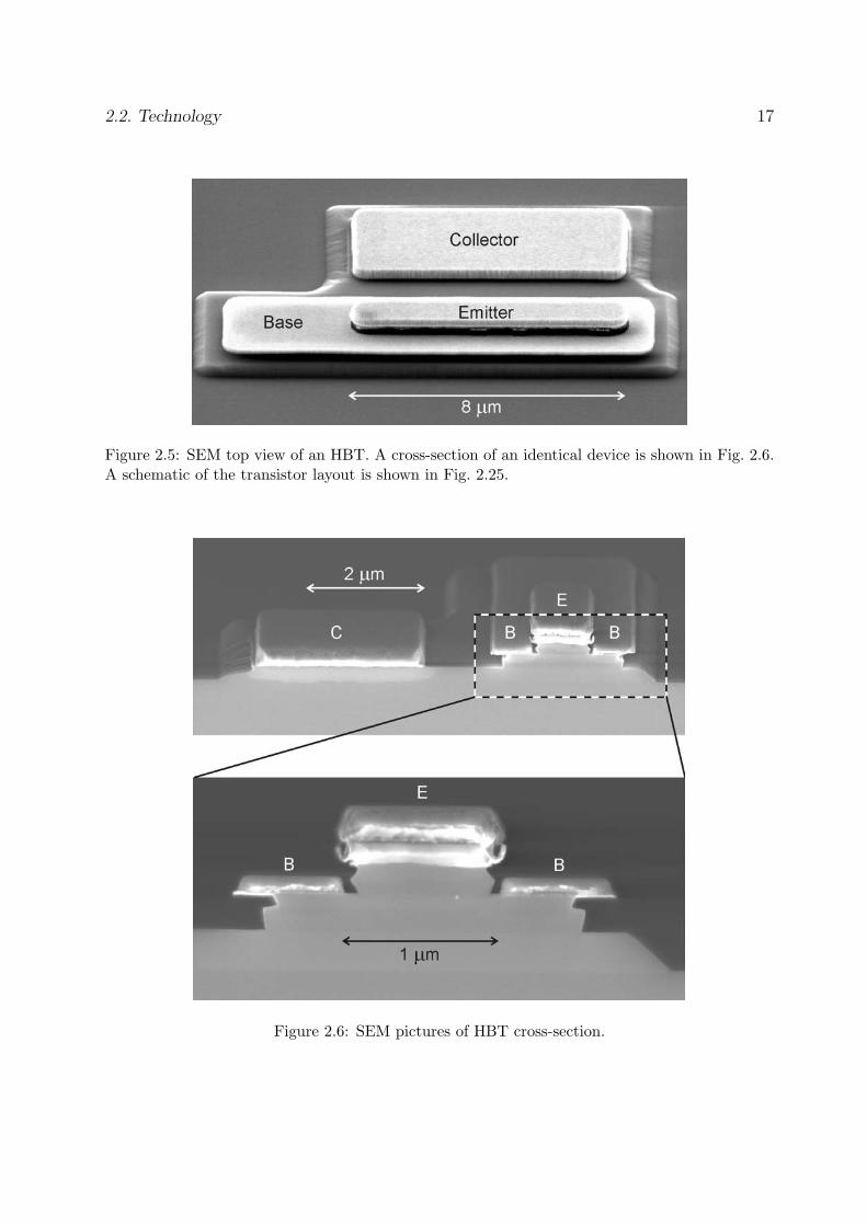
At Fraunhofer IAF the fabrication process of InP/InGaAs DHBTs and MMICs on 3-inchInP substrates is based on a standard triple mesa process [48]. This technology usesself-aligned base-emitter contacts and selective wet chemical etching. Scanning ElectronMicroscope (SEM) pictures of processed HBTs are shown in Figures 2.5 and 2.6. Ben-zocyclobutene (BCB) is used for device passivation and planarization. The collector andthe base are connected through via holes in the BCB. A schematic displaying all resultingelements of the process is depicted in Figure 2.7.
2.2. Technology 17
Figure 2.5: SEM top view of an HBT. A cross-section of an identical device is shown in Fig. 2.6.A schematic of the transistor layout is shown in Fig. 2.25.
Figure 2.6: SEM pictures of HBT cross-section.

18 2. InP-based Double Heterojunction Bipolar Transistor
Substrate
MET1MET1
VIA
VIA
Contact
Contact
ContactVIA
MET2 MET2
Galvanic
Galvanic
VIAEmitter
Base
Collector
SiNx
NiCr
BCB BCB
Figure 2.7: Schematic of the process showing elements available for circuit design including NiCrresistors and silicon nitride MIM capacitors.
The process includes thin film MIM capacitors (23 fF/μm2), NiCr resistors (50 Ω/�),and three levels of Au-based interconnect metals. The NiCr resistors are deposited onthe substrate and are connected using MET1 before BCB coating. The MIM capacitorsare realized using a thin layer of silicon nitride between the layers MET2 and Galvanicmetal. The Galvanic metal can also be used to realize airbridges. Therefore, three levelsof metalization can be used for interconnects.
2.2.2 Passive Structures
Coplanar waveguides (CPW) are used as transmission lines. As shown in Fig. 2.8, acoplanar waveguide consists of three conductors: one signal strip in the center and twoground conductors. The CPW technology is used, because it does not need a backsidemetallization, which is required for microstrip lines, and reduces the processing efforts.
The ground-to-ground spacing (d) of the coplanar lines in this work is 50 μm. Byvarying the width of the center conductor (w) the impedance of the transmission line can beadjusted. Formulas describing the impedance level are given in [42]. In the amplifier designsin Chapter 5 and 6 the center conductors have a width of 17 and 7 μm, corresponding toa line impedance of 50 and 69 Ω.

2.3. Layer Structure Optimization 19
d
w
substrate
groundground signal
Figure 2.8: Schematic of a coplanar waveguide cross-section.
2.3 Layer Structure Optimization
An optimized epitaxial layer structure is a prerequisite for high-performance transistors,as it determines the intrinsic device performance. The layer structure and the transistorlayout (s. Sec. 2.4) determine the values of the small-signal equivalent circuit elementsin Fig. 2.4. As explained above, two important figures of merit fT and fmax can be calcu-lated from these element values (s. Eqs. 2.5 and 2.6). Furthermore, the direct-current (dc)gain and power performance of the transistors depend on the layer structure.
This section describes how the experimental investigation of three different layer struc-tures standing for three development steps contributed to the optimization process. First,the results for an initial layer structure are presented. Features and deficiencies of the struc-ture are discussed. Following this, the results of two subsequent structures are presentedshowing how intended improvements could be realized by changing the layer structuresresulting in cut-off frequencies (fT, fmax) exceeding 250 GHz. Finally, the results of thissection are summarized.
2.3.1 Initial Layer Structure (A)
Emitter Layer
Considering the high-frequency performance of HBTs (s. Eq. 2.5), the contribution of theemitter to the total delay time is:
τe = Rje(Cje + Cbc)
In forward active mode the base-collector capacitance Cbc is much smaller than Cje andcan be neglected (s. Figs. 2.4 and 3.17). Hence, especially at low collector currents, wherethe differential resistance Rje of the emitter base diode has a considerable value, the base

20 2. InP-based Double Heterojunction Bipolar Transistor
Layer
Emitter
Base
Collector
Collector
Collector
Collector
Thickness (nm)
70
40
50
20
20
150
Semiconductor
InP
In Ga As: C0.53 0.47
In Ga As
In Ga As P
InP: Si
InP
0.53 0.47
0.85 0.15 0.32 0.68
Doping level (cm )-3
19
17
5.0 x 10
2.0 x 10
Layer Structure A
Figure 2.9: Schematic of layer structure A.
emitter capacitance Cje has a major impact on fT (Eq. 2.5). Thus, for high-frequency per-formance it seems advisable to keep the emitter junction capacitance low by implementinga long emitter depletion layer. It has been shown experimentally that a lightly dopedemitter with a relatively long emitter space charge region can result in higher values offT in comparison to emitters with high doping and a short space charge region [19]. Theextreme case of this concept is an undoped emitter [45], where the thickness of the emitterlayer alone determines the length of the space charge region and controlls the base emitterjunction capacitance. In our first structure (A) shown in Fig. 2.9 the latter concept isimplemented with an undoped emitter of 70 nm length in between the highly doped baseand cap layers.
Base Layer
The base layer affects the transit time of minority carriers in the base τb and the baselayer resistance Rbb. τb is a critical parameter for high-frequency performance (s. Eq. 2.5),because the only transport mechanism in the base is diffusion, unless a grading has beenimplemented. The base layer resistance Rbb has an effect on the relation between fT
and fmax (s. Eq. 2.6).
A reduction of the transit time of minority carriers in the base increases fT. Themobility of electrons has been reported to be larger than 3000 cm2/Vs in heavily p-typedoped (NA = 3.1 × 1019 cm−3) InGaAs base layers of InP-HBTs [13]. Therefore, the baselayer in InP-DHBTs is generally chosen to be of p-type [68]. Furthermore, to achieve asmall value for τb the base should be as thin as possible. A short transit time also has apositive effect on the current gain as the probability of recombination for each minoritycarrier crossing the base is small. However, the base layer resistance sets a lower limit forthe base thickness.
To keep the base layer sheet resistance Rbb small, the base doping should be veryhigh. The structures investigated were doped with carbon, which is the preferred p-typedopant for the base in this material system [10], [11], [28]. The doping level in this work

2.3. Layer Structure Optimization 21
is 5 × 1019 cm−3. However, even at such doping level, the InGaAs resistivity is noticeable.Therefore, the thickness of the base layer was chosen to be 40 nm to effect a compromisebetween short transit time τb and low base layer sheet resistance Rbb (Fig. 2.9).
Collector Layer
The collector layer has a major influence on both high-frequency parameters fT and fmax.From Eq. 2.5 the delay time associated with the collector is:
τ = τc + Cbc(RE + RC + Rje)
The first parameter τc describes the time electrons need to travel through the collector.The second term is the charging time constant of the base collector capacitance Cbc. Theresistances RE and RC reside outside the internal HBT and are determined by the metal-semiconductor contacts, the subcollector layer resistance and the resistance of the externalwiring. Rje depends on the emitter design and is small at normal operation in forwardactive mode. The maximum frequency of oscillation depends on fT and Cjc (s. Eq. 2.6).Therefore, regarding high-frequency performance the collector thickness is a compromisebetween short delay time τc (thin collector) and low capacitance values for Cbc and Cjc
(thick collector).Due to their large bandgap, InP layers in the collector of DHBTs can improve the
breakdown voltage, but they also tend to induce current blocking at the base-collectorjunction if an InGaAs base is used. If the collector design is poor, electrons propagatingthrough the space charge region can get caught at the barrier and rejected into the base.This reduces the dc current gain and causes additional storage of carriers in the collectordeteriorating the dc and high-frequency performance. A number of grading schemes havebeen developed to overcome blocking at the heterojunction [28].
Among various approaches, a thin n-doped InGaAs layer can be used to lower theconduction band spike [41]. Another concept employs a superlattice structure consistingof alternating InP/InGaAs layers with varying thickness helping to overcome the potentialbarrier in the conduction band [40]. Alternatively, a quaternary layer of InGaAsP withan intermediate band gap between that of InGaAs and InP can reduce the height of thepotential spike at the B-C junction [33]. In addition, a thin highly n-doped InP layer inthe collector can alleviate the current blocking effect [65]. This doping raises the Fermilevel at the peak of the barrier or, in other words, pulls down the effective barrier.
In structure A, the collector incorporates an InGaAsP step grading and a thin n-dopedInP layer adjacent to it (s. Fig. 2.9). The total thickness of the collector layer is 240 nm.A schematic band diagram of a DHBT with step graded collector is shown in Fig. 2.2.
Experimental Results
The characteristics of the layer structure were investigated by measuring an HBT with anemitter area of 10 μm2. The resulting output characteristic and Gummel plot are shownin Figs. 2.10 and 2.11, respectively.

22 2. InP-based Double Heterojunction Bipolar Transistor
Figure 2.10: Output characteristic of a transistor from layer structure A.
Figure 2.11: Measured Gummel plot of a transistor with an emitter area of 10 μm2 from layerstructure A.

2.3. Layer Structure Optimization 23
Figure 2.12: High-frequency parameters as a function of current density of an HBT with anemitter area of 10 μm2 from layer structure A (s. Fig. 2.9).
The turn on voltage in the output characteristic is approximately 0.3 V and the saturationvoltage (knee voltage) 0.7 V. The current gain extracted from the Gummel plot is 39. TheGummel plot also shows, that the leakage currents are below 1 nA and the ideality factorsfor base and collector current extracted at 1 μA are 1.3 and 1.2, respectively.
For high-frequency characterization, scattering parameters were measured using anAgilent 8510XF measurement system from 0.25 to 120 GHz (s. Sec. 4.2). From the gen-erated data the short-circuit current gain H21 and the unilateral gain U were calculatedand the high-frequency parameters fT and fmax extracted. The measurements were con-ducted with a collector-to-emitter voltage of 1.75 V, which typically resulted in optimizedhigh-frequency performance (compare Fig. 3.11). The results are shown as a function ofcurrent density in Fig. 2.12. The highest speed is reached at a collector current densityof 1.1 mA/μm2 reaching fT and fmax values of 150 and 210 GHz, respectively.
Discussion
The results demonstrate, that this first structure displays desirable features needed for thedesign of high-speed circuits. The maximum frequency of oscillation fmax exceeds 200 GHzand the current gain has an acceptable value of 39. From the process point of view, thelow leakage currents in the Gummel plot present a good result.
Nevertheless there are several points, which need to be improved. First, fT should alsoexceed 200 GHz. This is desirable, because the process is intended for digital as well asanalog circuits targeting high bit rates. The switching time in digital circuits strongly

24 2. InP-based Double Heterojunction Bipolar Transistor
Layer
Emitter
Base
Collector
Collector
Collector
Thickness (nm)
40
30
30
20
100
Semiconductor
InP: Si
In Ga As: C0.53...0.45 0.47...0.55
In Ga As
In Ga As P
InP: Si
0.53 0.47
0.75 0.25 0.54 0.46
Doping level (cm )-3
17
19
16
6.0 x 10
5.0 x 10
2.0 x 10
Layer Structure B
Figure 2.13: Schematic of layer structure B.
depends on fT and the bandwidth of distributed amplifiers depends on fmax [1]. As aconsequence, the goal of the optimization process is to achieve fmax ≈ fT. Second, the turn-on voltage and the saturation voltage ought to be decreased to enable operation at highercurrent densities without increasing the power consumption. Higher current densities wouldreduce the differential resistance Rje of the emitter-base junction (s. Eq. 3.6) and supporthigher values for the high-frequency parameters (s. Eqs. 2.5 and 2.6). Third, a largercurrent gain would be beneficial for the design of high gain amplifiers. These improvementscan be achieved by changing the layer structure. An improved layer structure is presentedin the following section.
2.3.2 Improved Layer Structure (B)
Emitter Layer
As discussed in the last section, a reduction of the turn-on voltage is desirable. This canbe achieved by changing the thickness and doping level of the emitter layer. In abruptInP/InGaAs emitter base junctions, the electron transport through the interface, where adiscontinuity in energy levels occurs (s. Fig. 2.2), is controlled by thermionic emission overand tunneling transmission through the spike [69]. However, in an undoped emitter, thespike barrier is wide enough, owing to the absence of n-type dopants, to prevent effectivetunneling [45]. Without tunneling a higher base-emitter voltage is needed to generate thesame emitter current resulting in a higher turn-on voltage [68]. Therefore, a higher dopinglevel and thinner emitter layer than in structure A are expected to reduce the turn-onvoltage. For layer structure B the emitter layer was chosen to have a thickness of 40 nmand a doping level of 6 × 1017 cm−3 (s. Fig. 2.13).
Base Layer
A key to improving the current gain and the cut-off frequency fT is a change in base layerdesign. In order to improve the current gain, an In grading is introduced in the base,which increases the band gap in the base gradually from the collector side to the emitter

2.3. Layer Structure Optimization 25
side. The indium mole fraction x is decreased from the lattice-matched value (0.53) at thebase-collector interface down to x = 0.53 − δx at the base-emitter interface. The inducedinternal built-in field has been shown to be very effective for reducing the transit time, i.e.,increasing fT, and reducing the recombination probability of the electrons in the base, i.e.,increasing current gain [66], [10]. The indium grading δx is maximized, while making thebase as thin as possible and accommodating the strain to prevent dislocations due to thelattice mismatch at the base emitter junction. In layer structure B (Fig. 2.13), a gradingof δx = 0.09 and a layer thickness of 30 nm are implemented.
The reduction in base thickness in comparison to structure A changes the ratio betweentransit time and layer resistance in favor of fT. This is acceptable since fmax is much higherthan fT in that structure, which suggests that Rbb is very small (s. Eq. 2.6).
Collector Layer
In structure A the high knee voltage and the low current densities are likely due to limi-tations in the collector layer design. The high saturation voltage seems to be caused by ahigh resistance at low collector-to-emitter voltages. At low bias voltages the collector spacecharge region might not be fully depleted and cause high layer resistances in non-depletedregions. This can be due to the large thickness of the collector, which results in relativelylow field intensities. Therefore, the collector for structure B was designed to be shorter.
A shorter collector will also influence the high-frequency parameters. The value forfT will increase as a result of a shorter collector delay time τc. On the other hand, thecollector capacitance Cjc will increase, which reduces fmax. However, this reduction mightget overcompensated by the increase in fT especially due to the changed base layer design.
A shorter collector should also enable higher current densities. The limitations instructure A are possibly due to the Kirk effect [55], [106]. At high current densities, theelectrons entering the collector from the base bear enough charge to neutralize the electricfield inside the collector. This prevents efficient field transport mechanisms and limitsdevice speed.
A shorter collector is also likely to result in a lower breakdown voltage. However, thebreakdown voltage of layer structure A is 6.1 V and a reduction is acceptable. A comparisonof the breakdown voltages of all layer structures investigated, is presented in Sec. 2.3.4.
Considering the arguments above, the all over collector length was reduced from 240 nmin structure A to 150 nm in structure B. As no current blocking could be observed instructure A, the moderately doped InP layer adjacent to the InGaAsP step grading wasreplaced by a lightly doped InP collector layer (compare Figs. 2.9 and 2.13).
Experimental Results
For characterization of structure B, the same device type, as the one investigated on theprevious structure, was measured. A comparison of the dc characteristics between deviceson layer structure B and A are given in Figs. 2.14 and 2.15. The turn-on voltage decreasedto 0.2 V. The saturation voltage increased to 0.8 V at high currents. The dc current gain

26 2. InP-based Double Heterojunction Bipolar Transistor
Figure 2.14: Comparison of output characteristics of transistors from layer structure B (solidlines) and layer structure A (dashed lines).
Figure 2.15: Comparison of Gummel plots of transistors with an emitter area of 10 μm2 fromlayer structure B (solid lines) and layer structure A (dashed lines).

2.3. Layer Structure Optimization 27
Figure 2.16: Comparison between layer structures B and A using high-frequency parameters ofan HBT with an emitter area of 10 μm2.
is more than twice as high as before, reaching a value of 80. The Gummel plot shows, thatthe leakage currents are still below 1 nA, and the ideality factors for base and collectorcurrent extracted at a current of 1μA are 1.5 and 1.1, respectively. In contrast to BJTs,DHBTs regularly feature different ideality factors for base and collector current, whichdepend in a complicated fashion on the design of the heterojunctions [68].
The measured high-frequency characteristics are shown in Fig. 2.16. As before, the mea-surements were conducted with a collector-to-emitter voltage of 1.75 V. The results showa cut-off frequency fT of more than 250 GHz and a maximum frequency of oscillation fmax
of almost 200 GHz at a current density of 1.8 mA/μm2.
Discussion
The measurement results demonstrate several improvements in comparison with the previ-ous layer structure. The turn-on voltage could be reduced and the current gain is doubled.The former result enables lower operating voltages and the latter enhances the capabilityto realize high gain amplifiers. These improvements are directly related to the change inemitter and base layer design. The graded base is responsible for the dramatic increasein β and fT. At the same time, higher current densities are possible, suggesting, that theKirk effect has been reduced.
However, there are still two parameters, which have to be improved. First, the satura-tion voltage at high currents is 0.8 V, which counteracts the low turn-on voltage. Second,the maximum frequency of oscillation, which did not rise at all, should be increased to

28 2. InP-based Double Heterojunction Bipolar Transistor
Layer
Emitter
Base
Collector
Collector
Collector
Collector
Thickness (nm)
40
30
50
20
20
70
Semiconductor
InP: Si
In Ga As: C0.53...0.45 0.47...0.55
In Ga As
In Ga As P
InP: Si
InP: Si
0.53 0.47
0.75 0.25 0.54 0.46
Doping level (cm )-3
17
19
17
16
6.0 x 10
5.0 x 10
2.0 x 10
2.0 x 10
Layer Structure C
Figure 2.17: Schematic of layer structure C.
roughly match the high value of fT. The limiting factor for both parameters is the effect ofcurrent blocking at the base-collector heterojunction. This effect does not only show in theoutput characteristic. The Gummel plot for structure B (Fig. 2.15) displays a kink for col-lector and base currents at 0.9 V, which is characteristic for this effect. The high-frequencyperformance is limited, because electrons accumulate at the heterojunction and increasethe charge storage in the collector. The current blocking effect and means to eliminate itwill be discussed in the following section.
2.3.3 Optimized Layer Structure (C)
The results of layer structure B show, that the new emitter and base layer designs ledto some of the desired improvements. The remaining deficiencies are mostly due to thecollector design. Therefore, emitter and base were not changed in the final structure (C).
Collector Layer
The discussion of structure B identified the phenomenon of current blocking as a problem,which is due to the conduction band potential barriers in the collector. It has been shownthat a potential barrier in the collector can cause a high saturation voltage in the outputcharacteristic (compare Fig. 2.14) and a low current density at the onset of current gaincompression [41]. Therefore, a reduction of this effect would lower the saturation voltageand enable transistor operation at higher current densities and higher speed.
In addition to the step graded collector, which is already implemented in layer structuresA and B, sophisticated doping profiles can reduce current blocking. If the doping level andthe resulting electric field is appropriate, blocking can be overcome [68]. However, if thefield intensity is insufficient, current blocking cannot be fully suppressed [65], which isprobably the case in structure B. On the other hand, if the electric field strength is toohigh, the collector cannot be fully depleted at a low collector bias, which is likely the reasonwhy the turn-on characteristic in layer structure A is poor.

2.3. Layer Structure Optimization 29
Consequently, a collector layer structure was chosen, which is a compromise betweenlayer A and B. The total length of the collector was hardly changed to keep high values forfT. However, a thin moderately doped InP layer was introduced adjacent to the InGaAsPstep grading. The layer is 20 nm thick and is also used in layer structure A. The new layerstructure (C) is shown in Fig. 2.17.
Experimental Results
The output characteristic of a device with an emitter area of 10 μm2 is shown in Fig. 2.18.The result does not show the blocking effect observed in layer structure B and the saturationvoltage is 0.7 V. The turn-on voltage is 0.2 V. A comparison of the output characteristicsof all three layer structures at IB = 200μA is given in Fig. 2.19. Figs. 2.20 and 2.21 showthe Gummel plot and the current gain, respectively. The Gummel plot is compared withthe results from structure B. The data show that the blocking effect is much weaker instructure C. The leakage currents in structure C are still below 1 nA and the idealityfactors for base diode and collector diode extracted from the Gummel plot at a currentof 1 μA are 1.4 and 1.1, respectively. The comparison of the current gains for all threestructures shows, that the maximum gain is 90 in the optimized structure (C), higher thanin the other structures.
Figure 2.18: Output characteristic of a transistor from layer structure C.

30 2. InP-based Double Heterojunction Bipolar Transistor
Figure 2.19: Comparison of output characteristics from different layer structures at a base currentof 200 μA. Layer structure C displays the lowest turn-on and saturation voltage as well as thehighest current gain.
Figure 2.20: Comparison of the Gummel plots from layer structure B and C. The current blockingin structure C is only weak, as the kink at 1 V is moderate.

2.3. Layer Structure Optimization 31
Figure 2.21: Comparison of the measured current gains from all three structures. The currentgain of structure C reaches 90 at its maximum and the current compression sets in at highercurrents than for the other structures.
Figure 2.22: Comparison of cut-off frequencies of transistors from three different layer structures.

32 2. InP-based Double Heterojunction Bipolar Transistor
Figure 2.23: Comparison of fmax of transistors from three different layer structrures.
Figure 2.24: Comparison of collector-to-emitter breakdown voltage of the three structures. Thedevices were measured with a collector current compliance of 10 μA. The resulting breakdownvoltages are 6.1 V for structure A, 4.8 V for structure B, and 4.2 V for structure C.

2.3. Layer Structure Optimization 33
The results of the RF measurements are shown as a function of current density inFigs. 2.22 and 2.23. The devices on structure C reach the highest speed at a collectorcurrent density of 3.0...3.5 mA/μm2, reaching fT and fmax values of 267 and 288 GHz,respectively. The comparison with layer structures A and B reveals, that the currentdensity as well as the speed is gradually increased from structure A to C.
Discussion
The change in collector design resulted in significant improvements. The saturation voltagewas decreased and the maximum frequency of oscillation was shifted upwards, significantly.Both improvements were realized by alleviating the current blocking effect. The electronscan cross the heterojunction barrier at low operating voltages, already, which has a positiveeffect on the saturation voltage. Also, the current gain compression is moved to highercurrent densities, enabling higher operating speed due to a lower value of the differentialresistance Rje at the emitter base junction (Eq. 2.5).
The elimination of current blocking prevents the accumulation of electrons at the barrierin the collector. This reduces the small-signal value for the base-collector capacitance sig-nificantly and is considered the reason for the tremendous increase in fmax when comparingstructures C and B (Fig. 2.23).
Structure C is optimized for dc and high-frequency operation. However, a fundamentallimitation of transistors is the trade-off between breakdown voltage and fT [79]. Accord-ingly, conservative measurements of the collector-to-emitter breakdown voltage BVCE0 witha current compliance of 1 μA/μm2 show a drop from 6.1 V for the initial structure (A)to 4.2 V for layer structure C (s. Fig. 2.24). From Table 2.1 it can be seen, that thebreakdown voltage decreases as the high-frequency parameters fT and fmax increase. InFig. 1.4 these results are compared to other semiconductor technologies. Apparently, thetradeoff between high-frequency performance and breakdown voltage is a fundamental rulefor HBTs and HEMTs for all listed semiconductor technologies. The smaller and faster thedevices get, the larger are the electrical field intensities inside the devices, and the smalleris the breakdown voltage.
2.3.4 Summary
The optimization process of the layer structure with respect to power and high speedis summarized in Table 2.1. It shows the major changes that were made in the layerstructure during the design process. Direct-current and high-frequency measurements wereused to analyze each layer structure. The analysis revealed limiting factors, which weresubsequently removed step by step. Correspondingly, the most important performanceparameters are listed, too. The data demonstrate that a thin emitter, a compositionallygraded base and a thin collector including a very thin moderately doped InP layer areimportant factors in the realization of high-speed DHBTs. The final optimized structurefeatures high-frequency parameters in excess of 260 GHz, which enable the development ofdigital as well as analog circuits at very high speed. At the same time the breakdown voltage

34 2. InP-based Double Heterojunction Bipolar Transistor
Summary of Layer Structure Optimization Process
structure A structure B structure C
emitter length (nm) 70 40 40doping no yes yes
base length (nm) 40 30 30composition uniform graded graded
collector length (nm) 240 150 160”delta” doping yes no yes
turn-on voltage (V) 0.3 0.2 0.2saturation voltage (V) 0.7 0.8 0.7
current gain 39 80 90fT (GHz) 150 255 267
fmax (GHz) 210 195 288BVCE0 (V) 6.1 4.8 4.2
Table 2.1: Comparison of the most important design and performance parameters of layer struc-tures A, B, and C. More details of the layer structures are given in the schematics in Figs. 2.9, 2.13,and 2.17.
is 4.2 V enabling the development of modulator drivers at power levels not conceivable insilicon based technologies (s. Fig. 1.4).
The layer structure, i.e. the vertical dimensions of a device, have been optimized in thissection. However, the lateral dimensions of a transistor are also important. The total areacovered as well as the geometry of a transistor influence its high-frequency performance.For this reason the next section deals with the optimization of the transistor layout.
2.4 Transistor Layout Optimization
Transistor layout is a critical issue in the development of high-performance transistors.These dimensions reflect in the parameter values of the small-signal equivalent circuit inFigure 2.4. Hence, the layout influences the device speed.
The geometry dependence of device performance has been investigated theoretically forhigh-speed devices and a good overview of this topic is given in [89]. Also several exper-imental results have been published. Among them are investigations of geometrical opti-mization of InP DHBTs with regards to speed [27], [15]. Also, for other HBT technologieslike SiGe and GaAs geometrical investigations have been conducted [112], [49], [103], [81].In addition, experimental data regarding power performance and thermal resistance asfunctions of geometrical dimensions are available [109].
However, it is very difficult to calculate the optimum dimensions of InP DHBTs fora desired performance for the following reasons. First, the investigations show, that theoptimization depends on the epitaxial layer structure. Second, besides layer structure

2.4. Transistor Layout Optimization 35
Subcollector Layer
CollectorContact
Substrate
Em
itte
rC
onta
ct
BaseContact
BaseMetal
Base Wiring
CollectorWiringLE
LC
LB
WB
WB
WB
WCWE
SBE
SBC
EmitterWiring
Figure 2.25: Schematic of HBT layout (top view).
and lateral dimension, process parameters like contact resistances and undercut etchingcan have a major impact on the results. In conclusion, the data from literature can giveguidelines but not accurate numbers for the geometrical layout of InP DHBTs optimizedfor highest speed.
Therefore, an analysis of devices with varying lateral dimensions was conducted. Theepitaxial layer structure in this investigation is the optimized layer structure discussedin the previous Section (Fig. 2.17). The optimized layout results in a device speed withparameter values of more than 280 GHz for fT and fmax.
The layout under investigation is shown in Fig. 2.25. It consists of rectangular shapes.An advantage of such a rectangular layout is the fact that extracted models scale withtransistor size to a certain degree (s. Sec. 3.3). In the following sections the dependenceof the high-frequency parameters fT and fmax on emitter size (LE, WE) and base contactwidth (WB) is investigated. The results confirm that a proper layout is critical for high-frequency operation and they indicate, how the performance could be further improved.The results are summarized in the last section.

36 2. InP-based Double Heterojunction Bipolar Transistor
2.4.1 Emitter Width Design
The design of the emitter width WE is guided by two major considerations. Currentcrowding effects as well as high values of the internal base resistance Rbb can degrade thetransistor performance.
Current crowding effects result from a voltage drop over the finite resistance of thebase layer caused by the base current flowing into the center of the base emitter junction.The effective base emitter voltage at the center of the junction is lower than at the edges.As a result the current density at the edges is higher than in the center and reduces theeffective base emitter junction area. In other words, the base-emitter junction capacitanceCje, which is proportional to the area of the junction, is larger than it needs to be. FromEquation 2.5 it can be seen, that this has negative consequences for fT. Another tech-nical drawback of a distributed nature of the emitter would be, that a more complicatedtransistor model than used in this work (Ch. 3) would be necessary.
The second straight forward consideration is the maximization of fmax. For a fixedemitter area fmax will be largest if Rbb is minimized (Eq. 2.6), i.e. if the ratio of perimeterto area is maximized. In conclusion, the narrowest emitter should result in the best high-frequency performance.
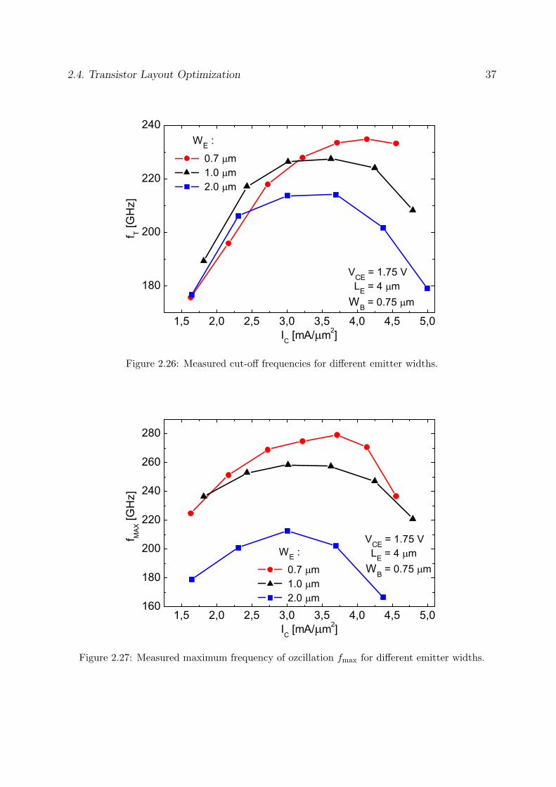
Experimental Results
Three different transistors with an emitter width WE of 2.0, 1.0, and 0.7 μm were analyzed.The devices investigated had an emitter length LE of 4 μm and a base width WB of 0.75 μm.The base and collector contact dimensions are described in Sections 2.4.2 and 2.4.3.
The results are shown as a function of current density in Figs. 2.26 and 2.27. Thesmaller WE is, the larger the maximum values for fT and fmax are. The cut-off frequencyand the maximum frequency of oscillation increase from 214 to 235 GHz and from 210to 280 GHz, respectively. Also, the current densities at which the maxima occur shift tohigher values as the emitter width decreases: from 3.5 to 4.1 mA/μm2 for fT and from 3.0to 3.7 mA/μm2 for fmax.
Discussion
The results show a strong dependence of the high-frequency performance on the emitterwidth WE. Especially fmax increases significantly for the narrow emitters. This increasecan be attributed to the reduction of the internal base resistance Rbb due to the changein perimeter to area ratio of the emitter (Eq. 2.6). The changes in cut-off frequencyand current density probably result from a reduction of current crowding. The narrowerthe emitter the more uniform the current distribution in the emitter is. As discussedabove, this leads to higher current densities and higher fT. However, these effects have aweaker influence on device performance than the reduction of Rbb. The results confirm theassumption, that the emitter should be as narrow as possible.
2.4. Transistor Layout Optimization 37
Figure 2.26: Measured cut-off frequencies for different emitter widths.
Figure 2.27: Measured maximum frequency of ozcillation fmax for different emitter widths.

38 2. InP-based Double Heterojunction Bipolar Transistor
2.4.2 Base Contact Width Design
Besides the emitter size, the base contact width WB and the base contact pad (LB, SBE)determine the dimensions of the internal transistor. Its size is proportional to the collectorcapacitance Cbc, which affects the high-frequency parameters of the transistors (Eqs. 2.5and 2.6). The smaller Cbc is, the higher the values for fT and fmax will be. From this pointof view, to achieve high cut-off frequencies, WB needs to be as small as technologicallypossible.
Depending on the quality of the base metal semiconductor contact, the base contactwidth WB can have a major impact on the base resistance RB. The transfer length ofa metal semiconductor contact is the length over which the current transfers from metalto semiconductor. In general, this length is longer for contacts displaying a high contactresistance and very short for contacts with negligible contact resistance [12]. Therefore, ifthe base contact width is smaller than the transfer length of the base metal contact, theparasitic base resistance RB will increase. This would result in a decrease of fmax, eventhough fT might rise. Hence, WB should not be smaller than the transfer length of thecontact.
The lengths LB and SBE are determined by the technology. LB and SBE add to thearea of the base collector junction which is proportional to Cbc. So, they should be assmall as possible, but large enough to ensure a reliable base contact to achieve high yieldin processing. For the current process the values of LB and SBE are 2.0 and 1.5 μm,respectively. An SEM picture of a HBT showing the base metal is shown in Fig. 2.5.
Experimental Results
Three different transistors with a base contact width WB of 1.0, 0.75, and 0.5 μm wereinvestigated. The devices had an emitter length LE and emitter width WE of 8 and 1 μm,respectively. The collector contact dimensions are described in Section 2.4.3. All measure-ments were conducted with a collector-to-emitter voltage of 1.75 V.
In Figs. 2.28 and 2.29 the results of the high-frequency measurements are shown as afunction of current density. Both parameters fT and fmax show an approximately linearincrease for decreasing values of WB. The cut-off frequency and the maximum frequencyof oscillation increase from 225 to 280 GHz and from 245 to 295 GHz, respectively. Thecurrent density at which the maxima occur is almost constant at ∼ 3.7 mA/μm2 for both fT
and fmax.
Discussion
The results document very clearly, how important the reduction of the parasitic basecollector capacitance is. Without changing the intrinsic transistor the performance couldbe increased, remarkably. The increase is of about the same magnitude for fT and fmax andconfirms that the assumptions based on Eq. 2.6 predict the high-frequency performance,correctly. Additionally, the transfer length of the base metal semiconductor contact isprobably shorter than 0.5 μm, because the increase in fmax appears to be linear and not

2.4. Transistor Layout Optimization 39
μμ
μ
μ
μ
μ
Figure 2.28: Measured cut-off frequency fT for various base contact width values.
μ
μ
μ
μ
μμ
Figure 2.29: Measurements of maximum frequency of oscillation fmax for various base contactwidth values.

40 2. InP-based Double Heterojunction Bipolar Transistor
saturated for the smallest base width. Therefore, a more advanced process, which canrealize shorter values for WB, should enable a further increase in high-frequency parameters.The fact that the current density for all maxima is the same, supports the argument of theprevious section, that the current density dependence is determined by the emitter layout,which is not changed in this section. In summary, the reduction of base contact width isvery effective way of increasing the high-frequency performance of HBTs.
2.4.3 Collector Contact Design
The collector contact design is determined by three parameters SBC , WC , and LC (Fig. 2.25).The contact is outside the active part of the device. The contact geometry affects mostlythe extrinsic collector resistance RC , which should be small to enable high-speed perfor-mance (s. Eq. 2.5).
Consequently, the spacing SBC should be as small as possible and has been fixedto 1 μm in this technology. The collector is designed to have twice the width of theemitter (WC = 2WE). This is large enough to ensure low resistance values and smallenough to enable compact circuit layouts. The collector length is set equal to the emitterlength (LC = LE) to provide a uniform current distribution in the collector.
2.4.4 Emitter Length Design
From a theoretical point of view, the emitter length LE is expected to have the followingeffects on the device performance. If the device is very small, the influence of the basecontact pad (LB, SBE) will be significant (Fig. 2.25). The experimental results from Sec-tion 2.4.2 show clearly, that the parasitic base collector capacitance is one limiting factorfor high-frequency performance. On the other hand, a very long emitter might reducethe device speed. Resistive and inductive effects in the narrow and long base contactsalong the emitter would be conceivable. Hence, especially for the optimization of LE anexperimental investigation is inevitable.
Experimental Results
Seven different transistors with emitter lengths varying from 2 to 16 μm were measured.The investigated devices had an emitter width WE of 1 μm and a base width WB of 0.75 μm.The base and collector contact dimensions were described in Sections 2.4.2 and 2.4.3. Allmeasurements were conducted with a collector-to-emitter voltage of 1.75 V.
The high-frequency results for four different emitter lengths are compared in Figs. 2.30and 2.31. Even though the current densities at which the maxima occur are not the same, aclear tendency is not apparent. The maximum value of fT starts at 225 GHz for LE = 4 μmand seems to saturate at 250 GHz for large emitter length values. The maximum frequencyof oscillation seems to reach a maximum of 270 GHz for an intermediate emitter length.

2.4. Transistor Layout Optimization 41
μ
μ
μ
μ
Figure 2.30: Dependence of fT on emitter length.
μ
μ
μ
μ
Figure 2.31: Dependence of fmax on emitter length.

42 2. InP-based Double Heterojunction Bipolar Transistor
μ
μ
μ
μ
Figure 2.32: fT and fmax vs. emitter length (solid lines: measurement, dashed lines: calculation).
To clarify this behavior, the high-frequency parameters for seven different devices at acurrent density of 3.5 mA/μm2 are plotted as a function of emitter length LE in Fig. 2.32.The cut-off frequency increases with emitter length, saturating at 250 GHz for long emit-ters (≥ 8 μm). The maximum frequency of oscillation shows a maximum of morethan 270 GHz at an emitter length of 6 μm with a sharp decrease for shorter emittersand a moderate decline for longer emitters.
For a more detailed analysis, small-signal models (s. Sec. 3.3) were extracted for eachtransistor at the operating points that correspond to the measured data points in Fig. 2.32.Using the extracted model parameters the high-frequency parameters fT and fmax werecalculated according to Equations 2.5 and 2.6 and included in Fig. 2.32. Calculated andmeasured data for fT match closely and although the calculation of fmax differs up to 10 %from the measured data, the principal behavior is described correctly.
Discussion
The results of this section reveal significant information. The length of the intrinsic emit-ter seems to have a much stronger influence on fmax than on fT. The decrease of bothhigh-frequency parameters for short emitter length can be attributed to the collector-basecapacitance of the base contact pad (s. Fig. 2.25), which has the same size for all de-vices. The shorter the emitter gets, the greater the influence of the additional parasiticcapacitance is.
Focusing emitter lengths larger than 6 μm, the scaling behavior can be seen. Thecut-off frequency fT seems to be almost independent of the emitter length, while fmax

2.4. Transistor Layout Optimization 43
gradually decreases with emitter length. A possible reason for the latter effect are resistiveand inductive effects in the narrow base contacts along the emitter (s. Fig. 2.25).
The scaling behavior of the high-frequency parameters can be explained using thesmall-signal parameters. A detailed discussion of these parameters and how they affectthe results summarized in Fig. 2.32 is given in Sec. 3.3, which deals with the small-signalmodel. Apparently, the choice of the emitter length is a compromise of minimizing theinfluence of the parasitic base contact pad and the influence of resistive or inductive effects.The latter effects seem unavoidable in high-speed HBTs with long emitters, as a narrowbase contact is a requirement for high speed (s. Sec. 2.4.2). The reduction of parasiticcapacitances depends also on the process technology. Therefore, it is difficult to propose ageneral design rule for the emitter length, and the choice of transistor size depends on thecircuit design requirements. For driver amplifiers critical considerations in addition to fT
and fmax are discussed in Sec. 6.1.
2.4.5 Summary
The experimental investigation of the transistor geometry (Fig. 2.25) produced the follow-ing results: as predicted by theoretical considerations, the base contact width WB andthe emitter width WE in Fig. 2.25 should be as small as possible. However, whilethe influence of WB on both frequency parameters is comparable, WE has a much strongereffect on fmax than on fT.
The choice of the emitter length LE depends on the size of the base contact pad (LB,SBE)and the base width WB. If the emitter is too short, both fmax and fT degrade very strongly(s. Fig. 2.32) due to the parasitic capacitance of the base contact pad. For very long emit-ters the maximum frequency of oscillation declines due to inductive and resistive effects inthe base contact.
The development of complex circuits requires high yield of devices. Depending oncircuit concepts amplifiers can consist of more than 50 transistors. The failure of onedevice can lead to a malfunction of the whole circuit and a layout that can be manufacturedreliably is crucial. Therefore, the geometrical dimensions of the devices used in amplifierdesign are chosen so, that the technological process provides a high yield on the devicelevel. This is achieved by slightly relaxing the dimensions in comparison to the smallestachievable values used in this investigation. The devices intended for circuit design areidentical to those, whose frequency performance is shown in Fig. 2.32. The final choiceof a particular transistor length LE at a certain point in a circuit depends onthe needed current, the speed requirements (fT, fmax), and also on input andoutput impedance of the devices (s. Sec. 6.1).
The discussion of this chapter shows, that the optimization of heterojunction bipolartransistors involves several issues, which are correlated. Process technology, the epitaxiallayer structure and the geometrical dimensions have to be optimized. First, differentepitaxial layers were investigated using high-frequency and dc measurements. From theresults, improved layer structures could be designed. Second, the geometrical layout ofthe transistors was optimized by investigating different transistors manufactured on the

44 2. InP-based Double Heterojunction Bipolar Transistor
optimized layer structure. As a result, InP DHBTs with high-frequency parameter values ofmore than 280 GHz for both fT and fmax could be realized, while maintaining a breakdownvoltage of over 4 V.

Chapter 3
Transistor Models
The transistor model is an important link between the process technology and the complexcircuit. On the one side it has to accurately describe the single device and can assist theoptimization and investigation of the transistors in a particular technology. On the otherside it is a necessary tool which makes the simulation and development of complex circuitspossible.
In principle, the modeling task could be fulfilled by a 3D-simulation of the carrier andfield distribution based on the physical parameters of each semiconductor layer and thetopology of the transistor structure. Particularly with regard to circuit simulation, suchan approach results in unacceptable long simulation times [85]. Therefore, a ”compact”model is needed, which describes the terminal behavior rather than the internal devicephysics.
Background
Although this work deals with analog circuits, its interaction with related research topicshas an effect on its methods. Concurrently, digital circuits for data rates up to 80 Gbit/swere developed at Fraunhofer IAF using the InP DHBT technology discussed in Chapter 2.Therefore, the modeling effort ought to provide a transistor model, which was equally suitedfor the development of analog as well as digital circuits. Low-power transimpedance ampli-fiers (TIA) and distributed amplifiers for higher output power levels like modulator driversoperate in the linear region of the devices. In contrast, digital circuits like multiplexersand demultiplexers are based on the nonlinear behavior of the transistors. Other buildingblocks of transmission systems like voltage controlled oscillators (VCO) and clock and datarecovery circuits require an accurate description of both kinds of characteristics.
Application to Circuit Design
The model described in this chapter was applied in the development of the amplifier circuitspresented in Chapters 5 and 6 [94], [95]. In addition, VCOs, multiplexers, and clock anddata recovery circuits suited for 80 Gbit/s applications have been developed, using the
45

46 3. Transistor Models
μ
Figure 3.1: Measured cut-off frequency fT of an InP-DHBT as a function of collector currentdensity for different collector-to-emitter voltages.
same model [73],[74],[72]. This shows that the modeling strategy described in this chapteris a suitable approach for the development of high-speed circuits for data rates at 80 Gbit/sand beyond.
Content
In the following section different large-signal models are discussed. Following this, anextraction procedure for the UCSD model is presented. The procedure’s starting pointresulted from a collaboration with the University of California, San Diego, and it wasadapted and refined to satisfy the needs of analog and digital circuit designs. In the lastsection, small-signal model results for transistor evaluation and optimization are presented.
3.1 Large-Signal Models
3.1.1 Gummel-Poon Model
The Gummel-Poon model was the first widely used large-signal model for bipolar transis-tors and is still considered a standard model for such devices. This model was proposedfor silicon bipolar transistors by Gummel and Poon in 1969 [38]. It is available in virtuallyall circuit simulators. However, DHBTs based on III-V technology display characteristicswhich are not accounted for by this model.

3.1. Large-Signal Models 47
Limitations
One of the salient features of InP- or GaAs-based HBTs, in contrast to Si-based bipolartransistors, is the strong bias dependence of the collector delay. This dependence is dueto the velocity modulation effect [46], which describes a non-monotonic dependence of theelectron velocity on the electric field. At low electric field all electrons reside in the socalled Γ-valley of the valence band. If electrons gain enough energy they can scatter intoa higher energy state in the L-valley. The effective electron mass in the L-valley is muchhigher than in the Γ-valley. In III-V semiconductors this reduces the electron velocitytremendously resulting in an increase of τc.
As the collector delay represents a significant portion of the total delay of an HBT,its variation is clearly visible in the fT characteristics of the device [47]. The resultingnon-monotonic dependence of fT on bias can be seen in Fig. 3.1. The graph shows thatthe high-frequency performance has a maximum at a collector-to-emitter voltage of 1.75 Vand a collector current density of 3.6 mA/μm2. In contrast to this behavior, the Gummel-Poon model assumes that the high-frequency performance improves with higher operatingvoltages at any given collector current level [68]. In addition, the model presumes that thedc current gain is independent of collector current over a wide range, which is not true forHBTs. Therefore, the Gummel-Poon model is not well suited for modeling InP-DHBTs.
3.1.2 Alternative Models
To overcome these limitations the following alternative large-signal models for HBTs havebeen proposed: With a focus on the accurate description of the collector delay time, anew model was developed at the Ferdinand-Braun-Institut fur Hochstfrequenztechnik [90].Partially built on the Gummel-Poon model other advanced models carefully treating self-heating and impact ionization effects were published [34], [51]. Based on previous work byCamnitz [18] the University of California, San Diego (UCSD) developed another model incollaboration with several industrial partners. The UCSD model [101] is the first model,which is dedicated to DHBTs in compound semiconductor technologies and which has alsobeen implemented in several commercially available simulators, among them Smart Spiceby Silvaco. Meanwhile, the capabilities of the UCSD model were further extended [47].This altered version has been implemented under the name AgilentHBT model in thesimulation software ADS by Agilent. In the following, the original version as well as thelatter version, are called UCSD model, because both models are almost identical, if asuitable subset of model parameters is used.
3.1.3 UCSD Model
In this work the UCSD model was used. It is available in two simulators, which were usedfor digital and analog circuit design, SmartSpice by Silvaco and ADS by Agilent. Othermodels described in Sec. 3.1.2 were not available in more than one simulation environment.Using commercial models helps to avoid convergence problems, which can occur if model

48 3. Transistor Models
Rbx
B
E
C
Re
Rci
Rcx
Qbe
QbcxQbciIbci
Ibcx
Ice
Ibe
Rbi
Figure 3.2: Equivalent circuit of the UCSD model displaying those components, that were utilizedfor modeling.
equations are not properly implemented. The model equations are freely available onthe internet [101]. The most important model equations and parameters are describedin Sec. 3.2.
Features
The model comprises features dedicated to DHBTs in III-V technology. A variety oftransit time parameters are provided to model the velocity modulation, which was alreadydiscussed above (s. Sec. 3.1.1). The collector current equation of the standard Gummel-Poon model is replaced by a more complex formulation. It takes into account the potentialspike, that can occur at the heterojunctions in HBTs, which causes a variation of currentgain with current density. In addition, thermal effects including self-heating and the Kirkeffect [55], which is responsible for the roll-off of the high-frequency parameters at highcurrents, can be modeled.
Topology
In contrast to the small-signal equivalent circuit (s. Fig. 2.4), the large-signal model usesa different topology for the intrinsic device (s. Fig. 3.2), which is called Π-topology. Largesignal models often inherit their Π-topology for historical reasons from the Gummel-Poonmodel. However, there exists a one-to-one correspondence between the T-Model and Π-Model [100]. Therefore, either topology can be used to model a transistor and for bothtopologies an equally accurate model can be extracted [35]. The T-topology of the small-signal model is derived from the device geometry (s. Fig. 2.3).

3.2. UCSD Model Extraction 49
3.2 UCSD Model Extraction
The extraction of a large-signal model was guided by the following considerations. First,an extracted model has to be suitable for both simulators, ADS (analog circuits) andSmartSpice (digital circuits). Second, only a subset of the vast number of more than 90parameters should be used. This reduces the time that is needed for model extractionas well as the simulation time. On the other hand, the accuracy of the model requiresa minimum amount of model parameters. Hence, a compromise between accuracy andcomplexity was made, which also allowed an easy transfer of models between simulatorenvironments.
For model extraction, the following simplifications were made. Model features concern-ing thermal effects were switched off. The parasitic capacitances between the transistorports and parasitic inductances at the transistor ports were neglected. Although these par-asitics have finite values, their behavior was modeled by adjusting the other parameters. Inaddition many parameters, which did not significantly enhance the model accuracy, weredisabled. A list of parameters that are being used and their extracted values are given inAppendix A.
The extraction of a model can follow different strategies. The model extraction is gener-ally assisted by the evaluation of dc and high-frequency measurements in different operatingpoints [97], [96]. The use of test structures in addition to transistor devices has also beenreported [23]. Numerical optimization of the parameters can also be applied [35], [47].
A collaboration with the UCSD provided a preliminary extraction procedure for theInP-DHBT used in this work. Subsequently, the extraction procedure was refined andadjusted. In particular, test structures were designed to assist the extraction of base andcollector resistances, which could not be extracted satisfactorily before. The deembed-ding procedure for high-frequency measurements was adopted from the small-signal modelextraction (s. Sec. 3.3). Additionally, the transistors were stressed before extraction toproduce devices, which resembled transistors in circuits under stress. The final extractionprocedure is described for a device with an emitter size of 8 × 1 μm2 in the followingsections.
3.2.1 Diode Parameters
The ideal diode characteristics, which are extracted from the Gummel plot, predict a linearrise of diode currents, if plotted on a log scale as in Fig. 3.3. Therefore, the extraction wasperformed at low currents, where the linear behavior can be observed. At high currents,other effects, e.g. due to series resistances, influence the Gummel plot and deteriorate theideal diode characteristic.
The reverse Gummel plot is shown in Fig. 3.4. The base current is accurately modeledfor medium and high current densities. The simulation and measurement of the emittercurrent do not match. The main reason is the fact, that the UCSD model does notprovide a diode parameter, which is exclusively dedicated to this current. The parameterdetermining this current is IS, which also determines the collector current in the forward

50 3. Transistor Models
Figure 3.3: Gummel plot comparing measured (solid lines) and simulated data (dashed lines).The model parameters IS, NF, ISE, and NE are extracted at low current densities from this plotin the marked range.
Gummel plot. As the forward active mode is the regular mode of operation in circuits, ISwas extracted from the forward Gummel plot.
One of the main features, which make the UCSD model distinct from the Gummel-Poonmodel, is the formulation of the equation for the collector-to-emitter current ICE (s. Fig. 3.2).If Webster and Early effects are neglected (compare Sec. 2.1), the equation simplifies to:
ICE =
exp
(q · Vbe
NF · k · T)− exp
(q · Vbci
NR · k · T)
1
ISAexp
(q · Vbe
NA · k · T)
+1
ISBexp
(q · Vbci
NB · k · T) (3.1)
The four parameters in the denominator NA, ISA, NB, and ISB are new parame-ters which are intended to describe the influence of the semiconductor heterojunctions.Vbe and Vbci are the potential differences between the internal nodes at the base-emitterand intrinsic base-collector diode. NF and NR are extracted from the Gummel dia-grams (Figs. 3.3 and 3.4). The other parameters are the electric charge (q), Boltzmann’sconstant (k), and the temperature (T ).
Theoretically, the parameters NA and ISA, which account for the influence of the base-collector heterojunction, could also be extracted from the forward Gummel plot. However,as can be seen from Fig. 3.3, the extracted model does not accurately describe the latterplot at high currents. This is due to the fact, that the base-collector bias condition atthe Gummel plot (VBC = 0 V) is different from the bias condition in forward active

3.2. UCSD Model Extraction 51
Figure 3.4: Reverse Gummel plot comparing measured (solid lines) and simulated data (dashedlines). The model parameters ISC, NC, and NR are extracted at medium current densities, wherethese parameters dominate the transistor behavior.
mode (VBC < 0V) in Fig. 3.5. The use of more model parameters should reduce themismatch in Fig. 3.3. However, as this large-signal model is intended for circuit design,the forward active mode (Fig. 3.5) needs to be described properly and the less accuratedescription of the Gummel plot is considered acceptable. In the output characteristic thegradual decrease of the measured collector current with increasing VCE is regularly observedand is due to self-heating.
3.2.2 Resistances
Often, the extraction of resistance is achieved by measuring the S-parameters of the devicein open collector mode or other special operating points. Using such purely S-parameterbased methods, we did not achieve satisfactory extraction results. Therefore, we developedtest structures, which allowed to get access to the resistance parameters by eliminating theinfluence of other parameters. Such methods have been successfully used before [23].
The test structures were designed to resemble the transistor as closely as possible. Still,the values that were measured were considered only close approximations and not accuratevalues. However, we found that these values enabled the extraction of a model. Never-theless, as a final extraction step, numerical optimization using the Levenberg-Marquardtalgorithm [82] was applied to the resistance parameters to improve the accuracy of themodel. As a result, some of the resistance parameters changed moderately. The optimizedvalues are listed in Tab. A.1.

52 3. Transistor Models
μΑ
Figure 3.5: Comparison of measured (solid lines) and simulated data (dashed lines). The currentsource parameters NB, ISB, NA, and ISA are extracted in the marked regions.
Collector Resistance
The collector resistance comprises two components. The extrinsic resistance accountingall resistances outside the internal transistor and the intrinsic collector resistance associ-ated with the subcollector layer resistance underneath the extrinsic base-collector junc-tion (s. Fig. 2.3). In the large-signal model the parameters RCX and RCI present theseresistances. They are extracted using a test structure shown in Fig. 3.6(a). By measuringsuch test structures of different dimensions the total resistance can be subdivided into anextrinsic and intrinsic part, which are defined as a subcollector layer sheet resistance RC�and a contact resistance RCcon. Tab. 3.1 shows the measurement results and the derivedresistances. In the derivation possible current spreading in the semiconductor layers wasneglected, because the doping of the subcollector is very high and the anticipated resistanceis small.
Using the estimated values for RC� and RCcon, the resistance parameters RCX and RCI
measurement results derived parametersy, z [μm] y = 2, z = 8 y = 4, z = 8 RC� [Ω/�] 20
2RCcon
z+
y
zRC� [Ω] 14 19 RCcon [Ωμm] 36
Table 3.1: Results of dc resistance measurements of the collector resistance test structurein Fig. 3.6(a) and corresponding derived resistance parameters. The results are average valuesfrom six separate measurements.

3.2. UCSD Model Extraction 53
Em
itte
r
Base
Colle
cto
rC
onta
ct
y
(a) Collector Resistance Test Structure
Colle
cto
rC
onta
ct
Wirin
g
Wirin
g
(b) Base Resistance Test Structure
Em
itte
r
Wirin
g
Wirin
g
Base
Base
Substrate
Subcolle
cto
r
Subcolle
cto
r
y
zz
RR RCONRCON
zzRCON
RCON
zzyy
zz
Figure 3.6: Schematic of test structures for extracting the resistance parameters RCX, RCI,RBX and RBI.
are calculated from the geometrical dimensions of the transistor:
RCX ≈ RCcon
LE
(3.2)
RCI ≈ RC�2
WE
LE
(3.3)
WE and LE are the emitter width and length (s. Fig. 2.25).
Base Resistance
The base resistance is divided in two components: the intrinsic base resistance RBI andthe extrinsic base resistance RBX. These parameters are extracted using a split base teststructure (s. Fig. 3.6(b)). The emitter-base junction of such a structure is very similar to aregular transistor. However, the base contact is split into two parts by extending the lengthof the emitter. From measuring such test structures with different values for y and constantz, approximations of the base resistance parameters can be derived. Tab. 3.2 summarizesthe results of several measurements and the inferred values for the sheet resistance of thebase layer (RB�) and the metal-semiconductor contact resistance (RBcon). Any resistancesof the base metal and wiring are neglected as other test structures revealed that their sheetresistance values are smaller than 0.2 Ω/�. Also, possible lateral current spreading effectsat the edges of the metal-semiconductor contacts were neglected.
To calculate the intrinsic base resistance RBI, the spacial contribution of the basecurrent has to be considered. Its current density decreases from the edges of the base-

54 3. Transistor Models
measurement results derived parametersy, z [μm] y = 1, z = 8 y = 2, z = 8 RB� [Ω/�] 880
2RBcon
z+
y
zRB� [Ω] 155 265 RBcon [Ωμm] 180
Table 3.2: Results of dc resistance measurements of the base resistance test structure in Fig. 3.6(b)and corresponding derived resistance parameters. The results are average values from six separatemeasurements.
emitter interface reaching zero in the center. For a narrow emitter the intrinsic baseresistance can be calculated using the following formula [68]:
RBI ≈ RB�12
WE
LE
(3.4)
The extrinsic base resistance parameter RBX is estimated by dividing RBcon by theperimeter of the base-emitter junction:
RBX ≈ RBcon
2(WE + LE)(3.5)
Emitter Resistance
The emitter resistance parameter RE accounts for the emitter resistance RE, which isthe sum of metal contact resistance and epitaxial layer resistances in the emitter caplayers (s. Figs. 2.3 and 2.17). The present technology (self-aligned) does not allow to designa test structure to directly measure the emitter resistance. Hence, the emitter resistanceis determined using a method proposed by Maas [70] and often applied in parameterextraction [92], [35], [105]. At low frequencies the real part of the small-signal two-portparameter Z21 of an HBT can be approximated by the sum of the emitter resistance RE
and emitter-base junction resistance Rje. The latter is inversely proportional to the emittercurrent IE. Therefore:
�{Z21} ≈ RE + Rje = RE +1
δIE
, (3.6)
where δ is a constant of proportionality.
By plotting �{Z21} versus 1/IE and extrapolating the graph towards 1/IE = 0, theemitter resistance RE can be extracted (s. Fig. 3.7) and its value is taken to be the param-eter RE. The measurement at any frequency in the range from from 3 to 10 GHz resultedin comparable resistance values.

3.2. UCSD Model Extraction 55
Ω
Figure 3.7: Graph showing the extraction of the emitter resistance by extrapolating the measureddata (solid line) to 1/IE = 0. The simulation (dashed line) using the extracted model confirmsthat this measurement well approximates the parameter RE.
3.2.3 Junction Capacitances
The small-signal capacitance of an abrupt pn-junction (Cpn) as a function of applied reversevoltage (Vbias) can be calculated to be [35]:
Cpn = Apnk√
Φ + Vbias
(3.7)
where Apn is the area of the junction, k is a function of the acceptor and donor dopinglevels, and Φ is the built-in voltage.
However, HBTs often feature complicated doping profiles (s. Sec. 2.3). Depending onthe profile Eq. 3.7 does not accurately describe the capacitance characteristics. Conse-quently, the model equations offer several additional parameters, which can be used toachieve an accurate extraction.
An established method for the extraction of the junction capacitance are reverse biasmeasurements [20]. In reverse bias a minimal amount of current is flowing and the ca-pacitive elements in Fig. 3.2 dominate the device’s response. In this state the small-signal capacitance values can be directly calculated from S-parameters. After measuringS-parameters and converting them into Y-parameters the base-emitter and base-collectorcapacitances (Cje, Cbc) are given by the following equations:
Cje =�{Y11 + Y12}
2πf(3.8)

56 3. Transistor Models
Figure 3.8: Comparison of measured (solid lines) and simulated data (dashed lines). The capac-itance parameters CJC and CJE are extracted at zero bias. All other parameters related to thejunction capacitances are extracted by fitting simulated to measured data.
Cbc =�{Y12}
2πf(3.9)
For model extraction the HBTs were measured under varying reverse bias and theassociated junction capacitances were calculated according to Eqs. 3.8 and 3.9. To improvethe accuracy of the results, the capacitance values were averaged over a frequency rangeof f = 3...8 GHz. The results are shown in Fig. 3.8. The capacitance values at zero biascorrespond to the model parameters CJE and CJC. The other model parameters arefitting parameters, which were adjusted accordingly. As can be seen from the comparisonof measured and simulated data, the parameter set of the large-signal model is well suitedto describe the junction capacitance of the devices.
3.2.4 Transit and Delay Times
Finally, the delay time parameters are extracted. Due to the dependence of the collectortransit time on collector current and collector-to-emitter voltage (s. Fig. 3.1) a large numberof 25 model parameters is provided (s. Appendix A). This prohibits a direct extractionof each parameter and numerical optimization has to be used. However, an estimation ofthe most important delay time parameters is advisable. This speeds up the optimizationprocess and increases the probability that an acceptable set of parameters is found, whichaccurately describes the transistor behavior.

3.2. UCSD Model Extraction 57
Parameter Estimation
Three parameters were estimated: the base transit time τb, the collector transit time τc andthe collector current at the onset of the Kirk effect IK . The transit time τb is approximatedusing the base layer semiconductor parameters. According to [68], the transit time forelectrons through a compositionally graded base (p-type) is given by the formulas
τb =WB
2
2Dn
f(k) ; Dn = μnkT
q; f(κ) =
2
κ(1 − 1
κ+
1
κe−κ) ; κ =
ΔEG
kT, (3.10)
where WB is the thickness of the base layer, Dn is the diffusion constant for electrons, κis the electric field factor, μn is the mobility of electrons, k is Boltzmann’s constant, Tis the temperature, q is the elementary charge, and ΔEG is the change in bandgap dueto the grading. WB is 30 nm (Fig. 2.17). The electron mobility in highly p-type dopedInGaAs-layers has been reported to be μn ≈ 3000 cm2/(Vs) [13]. Although this result hasnot been confirmed by other authors, we are using this value for estimation. Consideringthe strain, which is introduced by the compositional grading specified in Sec. 2.3.2, andusing reported experimental data [102] ΔEG was estimated to be 50 meV. Applying allthis information to equation above, it follows τb ≈ 34 fs, which was taken as starting pointfor model parameter TFB.
The transit time τc can be calculated using Eq. 2.5 and Rje = 1δIE
(s. Eq. 3.6):
τc =1
2πfT
− 1
δIE
(Cje + Cbc) − Cbc(RE + RC) − τb (3.11)
The resistance RE equals the previously extracted parameter RE and RC is approximatedto be RCX + RCI. The factor 1
δis extracted from the slop of the graph in Fig. 3.7.
The other parameters depend on the bias condition. For VCE = 1.75 V and IE = 21 mAthe paramters fT and Cbc were taken from Figs. 3.10 and 3.8, respectively. Cje was ap-proximated to be equal to the small-signal parameter CE (s. Fig. 3.17). This resulted inan estimation of τc ≈ 205 fs and was taken as the starting point for model parameterTCMIN .
The current IK is taken from Fig. 3.10 and marks the current, at which the high-frequency parameter start to decrease (25 mA; starting point for model parameter IKRK).
Optimization
The extraction of the delay time parameters is performed by fitting the high-frequencyparameters fT and fmax over a wide range of operating points. The high-frequency param-eters are obtained using a generally accepted method for high-frequency characterizationof transistor devices [88]. First, the unilateral gain U and the two-port parameter H21
are calculated from the measured and simulated S-parameters. Then the curves are inter-polated with a straight line at a slope of -20 dB/dec to the frequency points, where theparameters have decreased to unity (s. Fig. 3.9).

58 3. Transistor Models
Figure 3.9: The graph shows how the high-frequency parameters fT and fmax are obtained byextrapolating the small-signal current gain (H21) and the unilateral gain (U).
Figure 3.10: fT and fmax as a function of collector current IC . Comparison of measured (solidlines) and simulated data (dashed lines).

3.2. UCSD Model Extraction 59
Figure 3.11: fT and fmax as a function of collector-to-emitter voltage VCE . Comparison ofmeasured (solid lines) and simulated data (dashed lines).
The optimization process was started with the estimated parameter values from aboveand very few additional parameters. As expected the fit was very poor. Gradually, moreand more parameters were included in the optimization and, simultaneously, the differ-ence between measured and simulated data could be reduced. After allowing all delayparameters to be optimized, the curves shown in Figs. 3.10 and 3.11 were achieved. Theydemonstrate that the current dependence as well as the voltage dependence of the high-frequency parameters can be correctly modeled. The ability to model their non-monotonicdependence on VCE (s. Fig. 3.11) is a feature of the UCSD model, which the Gummel-Poonmodel cannot provide.
Comparing the estimated and optimized values for TFB, TCMIN , and IKRK sug-gests some interesting information about the model. The base transit time parameter andthe Kirk current parameter have only moderately changed. It seems that these parame-ters have a physical meaning like the diode parameters which were extracted directly frommeasured data without optimization. In contrast, TCMIN has dramatically changed,which indicates that it is a parameter, which is not directly related to the collector transittime. However, these observations are not supported by hard evidence and were not furtherinvestigated.
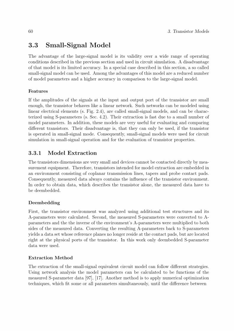
60 3. Transistor Models
3.3 Small-Signal Model
The advantage of the large-signal model is its validity over a wide range of operatingconditions described in the previous section and used in circuit simulation. A disadvantageof that model is its limited accuracy. In a special case described in this section, a so calledsmall-signal model can be used. Among the advantages of this model are a reduced numberof model parameters and a higher accuracy in comparison to the large-signal model.
Features
If the amplitudes of the signals at the input and output port of the transistor are smallenough, the transistor behaves like a linear network. Such networks can be modeled usinglinear electrical elements (s. Fig. 2.4), are called small-signal models, and can be charac-terized using S-parameters (s. Sec. 4.2). Their extraction is fast due to a small number ofmodel parameters. In addition, these models are very useful for evaluating and comparingdifferent transistors. Their disadvantage is, that they can only be used, if the transistoris operated in small-signal mode. Consequently, small-signal models were used for circuitsimulation in small-signal operation and for the evaluation of transistor properties.
3.3.1 Model Extraction
The transistors dimensions are very small and devices cannot be contacted directly by mea-surement equipment. Therefore, transistors intended for model extraction are embedded inan environment consisting of coplanar transmission lines, tapers and probe contact pads.Consequently, measured data always contains the influence of the transistor environment.In order to obtain data, which describes the transistor alone, the measured data have tobe deembedded.
Deembedding
First, the transistor environment was analyzed using additional test structures and itsA-parameters were calculated. Second, the measured S-parameters were converted to A-parameters and the the inverse of the environment’s A-parameters were multiplied to bothsides of the measured data. Converting the resulting A-parameters back to S-parametersyields a data set whose reference planes no longer reside at the contact pads, but are locatedright at the physical ports of the transistor. In this work only deembedded S-parameterdata were used.
Extraction Method
The extraction of the small-signal equivalent circuit model can follow different strategies.Using network analysis the model parameters can be calculated to be functions of themeasured S-parameter data [97], [17]. Another method is to apply numerical optimizationtechniques, which fit some or all parameters simultaneously, until the difference between

3.3. Small-Signal Model 61
μΩ
Figure 3.12: Measured (solid lines) and simulated (dashed lines) scattering parameters using thesmall-signal model.
μΩ
Figure 3.13: Measured (solid lines) and simulated (dashed lines) scattering parameters using thesmall-signal model.

62 3. Transistor Models
μΩ
Figure 3.14: Measured (solid lines) and simulated (dashed lines) scattering parameters using thelarge-signal model.
μΩ
Figure 3.15: Measured (solid lines) and simulated (dashed lines) scattering parameters using thelarge-signal model.
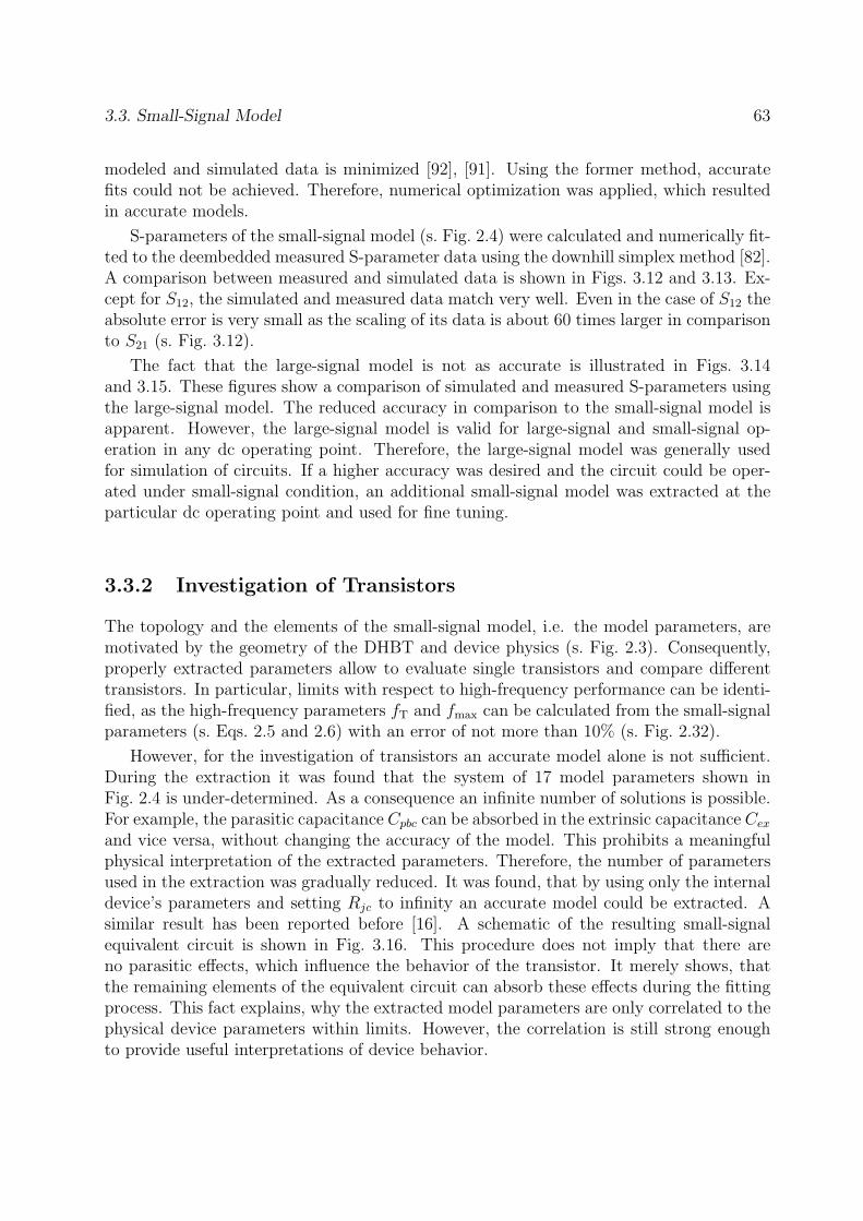
3.3. Small-Signal Model 63
modeled and simulated data is minimized [92], [91]. Using the former method, accuratefits could not be achieved. Therefore, numerical optimization was applied, which resultedin accurate models.
S-parameters of the small-signal model (s. Fig. 2.4) were calculated and numerically fit-ted to the deembedded measured S-parameter data using the downhill simplex method [82].A comparison between measured and simulated data is shown in Figs. 3.12 and 3.13. Ex-cept for S12, the simulated and measured data match very well. Even in the case of S12 theabsolute error is very small as the scaling of its data is about 60 times larger in comparisonto S21 (s. Fig. 3.12).
The fact that the large-signal model is not as accurate is illustrated in Figs. 3.14and 3.15. These figures show a comparison of simulated and measured S-parameters usingthe large-signal model. The reduced accuracy in comparison to the small-signal model isapparent. However, the large-signal model is valid for large-signal and small-signal op-eration in any dc operating point. Therefore, the large-signal model was generally usedfor simulation of circuits. If a higher accuracy was desired and the circuit could be oper-ated under small-signal condition, an additional small-signal model was extracted at theparticular dc operating point and used for fine tuning.
3.3.2 Investigation of Transistors
The topology and the elements of the small-signal model, i.e. the model parameters, aremotivated by the geometry of the DHBT and device physics (s. Fig. 2.3). Consequently,properly extracted parameters allow to evaluate single transistors and compare differenttransistors. In particular, limits with respect to high-frequency performance can be identi-fied, as the high-frequency parameters fT and fmax can be calculated from the small-signalparameters (s. Eqs. 2.5 and 2.6) with an error of not more than 10% (s. Fig. 2.32).
However, for the investigation of transistors an accurate model alone is not sufficient.During the extraction it was found that the system of 17 model parameters shown inFig. 2.4 is under-determined. As a consequence an infinite number of solutions is possible.For example, the parasitic capacitance Cpbc can be absorbed in the extrinsic capacitance Cex
and vice versa, without changing the accuracy of the model. This prohibits a meaningfulphysical interpretation of the extracted parameters. Therefore, the number of parametersused in the extraction was gradually reduced. It was found, that by using only the internaldevice’s parameters and setting Rjc to infinity an accurate model could be extracted. Asimilar result has been reported before [16]. A schematic of the resulting small-signalequivalent circuit is shown in Fig. 3.16. This procedure does not imply that there areno parasitic effects, which influence the behavior of the transistor. It merely shows, thatthe remaining elements of the equivalent circuit can absorb these effects during the fittingprocess. This fact explains, why the extracted model parameters are only correlated to thephysical device parameters within limits. However, the correlation is still strong enoughto provide useful interpretations of device behavior.

64 3. Transistor Models
B
EE
C
Rje
i’e
Cje
CjcCbc=C +Cjc ex
Cex
Rbb
�0ei��T
Figure 3.16: Equivalent circuit displaying elements that were needed to extract an accuratesmall-signal model.
Experimental Results
The transistors intended for circuit design were further investigated. These transistorshave an emitter length varying from 2 to 16 μm. The other geometrical parameters areconstant (base contact width WB = 0.75 μm, emitter width WE = 1 μm, s. Fig. 2.25).The devices provide a compromise between high speed and high yield on the device level.Their design is the result of an optimization of device geometry (s. Sec. 2.4).
Small-signal models for all devices were extracted at a collector-to-emitter voltageVCE = 1.75 and a collector current density of 3.5 mA/μm2. The model parameter val-ues as a function of emitter length are shown in Figs. 3.17, 3.18, and 3.19. The larger theemitter length the larger the capacitances are and the smaller the resistance values get.While the parameters Cex and Cje scale linearly, the intrinsic base-collector capacitanceCjc seems to scale quadratically. The resistance parameters Rje and Rbb scale linearly with1/LE with the exception of the shortest emitter length (2 μm). The transit time τT andα (Fig. 3.19) are approximately independent of emitter length for LE > 2 μm. In thesame figure two product terms Cje · Rje and Cjc · Rbb are plotted, of which the first oneis constant and the second slightly increases with emitter length, if the shortest emitterlength is neglected, which is affected by high value for Rbb.
The transistor with the shortest emitter length (2 μm) showed strong degradation andreliability problems during the measurement procedures. The origin of this degradationhas been correlated to some limits in the present process technology such as device layoutand layer structure composition. In effect, the aggressive down scaling of the emitter sizelikely results in an increase in the emitter cap to metal contact resistance. This causes thecorresponding small-signal parameter values to deviate from the scaling behavior of theother devices. To overcome this problem, an incorporation of an InAs contact layer in theemitter cap has been shown to improve the device performance, as reported in [39].

3.3. Small-Signal Model 65
μ
Figure 3.17: Graphical representation of capacitance parameter values versus emitter length.Except for Cjc the scaling behavior is linear. The non-linear scaling of Cjc is considered to becaused by parasitic effects.
Ω
μ
Ω
Figure 3.18: Resistance parameter values versus emitter length. Both parameters scale inverselyproportional to emitter length. The parameter values for the shortest emitter length seem not tofollow the scaling behavior as closely as the other data points. This is attributed to limitationsin the present process technology with such small devices (compare Fig. 3.19).

66 3. Transistor Models
α
τ
μ
τ
α
Figure 3.19: Parameter values of τT and α as well as the product terms Cje · Rje and Cjc · Rbb
as a function of emitter length. The increase in τT and Cje · Rje for LE = 2 μm is attributed toscaling limitations in the present process technology resulting in performance degradation.
Discussion
The results reveal some interesting information about the transistors. Especially the de-pendence of the high-frequency parameters fT and fmax on emitter length can be under-stood. In the following discussion the smallest transistor with emitter length LE = 2 μmis neglected as it showed a degradation which is due to the present process technology.
First of all, most parameters seem to scale with emitter size as expected from physicaland geometrical considerations. The capacitances increase proportional to the increase insize and the resistances increase with the inverse of emitter length. The transit time τT
and the base transport factor α are almost constant. This is plausible as these parame-ters depend on the vertical electron transport mechanisms, which are determined by theepitaxial layer structure and not by device geometry.
However, the intrinsic base-collector capacitance Cjc does not scale linearly with emitterlength, but rather quadratically (s. Fig. 3.17). This behavior is attributed to parasiticeffects. The topology of the extracted small-signal model (Fig. 3.16) does not provideadditional parameters to account for parasitics, because they are not needed to extractmodels with high accuracy. Consequently, the influence of the parasitic effects is absorbedby the other parameters, which manifests in the non-linear dependence of Cjc on emitterlength.

3.3. Small-Signal Model 67
The cut-off frequency fT and the maximum frequency of oscillation fmax of the dis-cussed devices are shown in Fig. 2.32. The measured values are plotted as a function ofemitter length. In addition, the small-signal parameters extracted in this section wereused to calculate and plot fT and fmax applying Equations 2.5 and 2.6. Measurement andcalculation are correlated closely enough to enable an interpretation of the measurementresults using the small-signal model parameters of this section.
The decrease of both high-frequency parameters for short emitter length can be at-tributed to the collector-base capacitance of the base contact pad (s. Fig. 2.25), whichhas the same size for all devices. This can be seen in Fig. 3.17, where a linear interpo-lation of the parameter Cex, which is associated with the extrinsic collector base capaci-tance (s. Fig. 2.3), appears to result in a considerable value for a device of emitter lengthzero. The shorter the emitter gets, the greater the influence of the additional parasiticcapacitance is. The effect, that a comparatively large extrinsic base-collector capacitanceseriously reduces the high-frequency performance of a transistor, was already shown inSec. 2.4.2. For this reason the base contact pad as well as the base contact width werechosen to be as small as possible in the present process technology. For emitter lengthexceeding 8 μm the influence of the base contact pad seems to become negligible.
Focusing on long emitter lengths, the scaling behavior of the device neglecting the basecontact pad can be seen. The cut-off frequency fT seems to be almost independent of theemitter length. The reason is, that the delay time τT and the product of Rje and Cje areapproximately constant for any emitter length (s. Fig. 3.19) and dominate the result ofEquation 2.5 for long emitter length, where Cje is much larger than the other capacitanceparameters (s. Fig. 3.17).
An explanation for the scaling behavior of fmax at long emitter length is offered byequation 2.6 and the extracted small-signal model parameters. Any variation of the ratiobetween fT and fmax depends on the product of Rbb and Cjc, whose value is plotted inFig. 3.19 as a function of emitter length. For emitter lengths larger than 6 μm the valuesgradually increase explaining the decrease of fmax. The increase of this product term isprobably due to parasitic effects, which are absorbed by the model parameters Rbb and Cjc.Especially Cjc does not scale linearly, which would be unexpected, if the parameter didonly depend on the intrinsic collector capacitance. Possible reasons for this observation areresistive and inductive effects in the narrow base contacts along the emitter (s. Fig. 2.25).This is conceivable, if the current flow is considered. The emitter and collector wiring isarranged in such a way that the current densities for all emitter lengths are comparable.However, the base current flows along the emitter through the narrow base contact, whichdoes not scale in width with emitter length. As a consequence, the finite resistance of thecontact could become significant. In addition, the skin effect in the narrow contact couldplay an important role, which was neglected in the derivation of the small-signal modeltopology (s. Figs. 2.3 and 2.4).

68 3. Transistor Models
3.4 Summary
In this chapter the large-signal UDSD model as well as a small-signal model were describedand their contributions to the design of high bit rate circuits and the investigation oftransistors were explained. Starting from a preliminary status the extraction procedurefor the large-signal model could be refined and adjusted to the demands of designingdigital and analog circuits targeting 80 Gbit/s. In this process a suitable compromisebetween complexity and accuracy was made. These models successfully contributed to therealization of state-of-the-art analog and digital circuits [94], [74], [72].
The small-signal model is a very useful tool in addition to the large-signal model. Eventhough it is only valid in small-signal operation, its accuracy is higher and the extractionis faster than in the large-signal case. It can be used for fine tuning of the small-signalresponses of amplifiers. In addition, it can be used to investigate transistors. Extractedmodel parameters were used to explain the complicated dependence of the high-frequencyparameters fT and fmax on emitter length.

Chapter 4
Methods of Broadband AmplifierCharacterization
4.1 Figures of Merit
Most optical communication systems employ binary amplitude modulation using the ”non-return to zero” (NRZ) data format [86]. The transmitted data signals experience variousimperfections in the optical and electrical domain, which can increase the bit error rate(BER) or even make a transmission of data impossible. To evaluate the performance ofsystem components, different figures of merit (FOM) can be defined, in addition to theBER. For broad-band amplifiers suitable as modulator drivers bandwidth, group delay andoutput power are important. These FOMs support the interpretation of the experimentalresults in Chapters 5 and 6.
4.1.1 Bandwidth
In digital communications systems, the available bandwidth is limited, because many sys-tem components, e.g. amplifiers, have limited bandwidth. For this reason, it is importantto consider the spectral content of the digitally modulated signals in order to design suit-able amplifiers. Calculations show, that the spectral shape of a random binary sequence inNRZ data format is determined by the spectral characteristic of a single signal pulse [83].
A comparison of two different signal pulses and their power density spectra is shownin Fig. 4.1. In the time domain, the rectangular pulse u�(t) (dashed line) of length T hasthe ideal shape for data transmission at a bit rate of 1/T with a rise and fall time of zero.The raised cosine pulse ucos(t) (solid line) has twice the length in the time domain and arise an fall time of length T.
In the frequency domain, the spectral power density of the raised cosine pulse |Ucos(f)|2(solid line) is almost entirely confined to frequencies below 1/T. In contrast, the rectangularpulse has noticeable frequency components (|U�(f)|2, dashed line) at frequencies greaterthan 1/T. An explanation for this behavior is given by the equations for both pulses in the
69

70 4. Methods of Broadband Amplifier Characterization
time domain frequency domain
t
u(t) U(f)
T2
A2
T2
T2
T1
T1
T3
T3T
2T
A A T
-T f
2
2
2
- - --0 0
Figure 4.1: Time and frequency representation of raised cosine pulse (solid lines) in comparisonto the rectangular pulse (dashed lines). Analytic formulas are given in Eqs. 4.1 to 4.4.
time domain and their Fourier transforms (s. Eqs. 4.1 to 4.4). In contrast to the rectangularpulse, the Fourier transform of the raised cosine pulse decays inversely as f 3.
u�(t) = A ; |t| <T
2(4.1)
U�(f) = ATsin πfT
πfT(4.2)
ucos(t) =A
2
[1 + cos
πt
T
]; |t| < T (4.3)
Ucos(f) = ATsin 2πfT
2πfT (1 − 4f 2T 2)(4.4)
Electrical digital circuits always generate signal pulses with finite rise and fall times.These delay times depend not only on the high-speed performance of the transistor, butalso on the circuit concept. E.g., the current switch, a fundamental building block of digitalcircuits, utilizes not only transistors, but also resistors. These resistors, in combination withthe intrinsic and parasitic capacitances of the transistor, give rise to delay time constants,which affect the shape of the signal pulses. As a result, high-speed NRZ data signalstypically have a shape which is close to the raised cosine pulse, which can be seen in theeye diagram in Fig. 4.4 (top). The eye diagram shows the superposition of a pseudo randombit sequence, which is generated by a 80 Gbit/s electrical multiplexer (s. Sec. 4.3.2).
Although the shape of the signal pulses is not exactly a raised cosine pulse, the similaritycan be used to interpret the eye diagrams in Fig. 4.4 in the following way. First, the factthat the pulses have a raised cosine like shape (top figure) implies, that the bandwidth ofthe data signal is probably not greater than 80 GHz (s. Fig. 4.1) and that this bandwidth issufficient to transmit digital signals in NRZ data format at a data rate of 80 Gbit/s. Second,from the middle and bottom figure we conclude, that a further reduction in bandwidth

4.1. Figures of Merit 71
results in even broader and not as clearly modulated signal pulses, which increases theBER and eventually makes data transmission impossible. This is discussed in more detailin Sec. 4.3.2.
The degradation of the ideal rectangular pulse of length T to a pulse with finite rise andfall times with a pulse length greater than T is also called intersymbol interference (ISI) [86],as each pulse interferes with the preceding and succeeding pulses. The discussion aboveshows that ISI can be cause by a limitation in bandwidth, but that a bandwidth of 1/Tis still sufficient for data transmission. However, ISI is also influenced by characteristicsother than bandwidth, i.e., group delay described in the following section.
4.1.2 Group Delay
Dispersion is a familiar phenomenon in electronics. If different frequencies comprisinga pulse propagate at different velocities in a medium or system component, then phasedistortion occurs and the pulse shape can change. Group delay is a useful measure ofphase distortion in components such as amplifiers and filters. It measures the transit time,with respect to frequency, of a signal through the device under test. The group delay Tg
is calculated as the derivative of the phase response with respect to frequency [3]:
Tg =dΦ
dω(4.5)
The pulse shape does not change, if the group delay is constant over the full width ofits spectrum. In broadband amplifier design, this is not always the case, because specialdesign techniques like peaking mechanisms (s. Sec. 6.1.2) can cause resonance effects withinthe amplifier, which can seriously affect the group delay flatness. Therefore, in amplifierdesign group delay is an important design criterion. Evaluating the group delay has beenused before to assess the quality of broadband amplifiers [95] and can be used to estimatethe possible strength of ISI. However, eye diagrams are the preferred method of character-ization (s. Sec. 4.3.2), because they show the overall effect of ISI on the quality of the datasignal.
4.1.3 Output Power
The output power is an important FOM for amplifiers used as modulator drivers. Themodulator at the transmitter side of an optical communication system (s. Fig. 1.2) can berealized using different materials and concepts [24]. The most commonly used materials forexternal modulators are LiNbO3, III-V compound semiconductors, and electric polymers.They are used to realize Mach-Zehnder (MZ) and electroabsorption (EA) modulators.Common for all modulator concepts is the fact, that an acceptable extinction ratio ofthe optical modulated signal can only be achieved, if the voltage swing of the electricalsignal driving the modulator matches or exceeds a certain value, which depends on thematerials and concepts. Recently, a traveling-wave EA modulator suitable for 80 Gbit/swas reported, which required a voltage swing of 3 V peak-to-peak delivered to a 50 Ω

72 4. Methods of Broadband Amplifier Characterization
Figure 4.2: Photograph of S-parameter measurement system HP 8510XF.
load [111]. Therefore, modulator drivers should deliver a voltage swing of at least 3 V ina 50 Ω circuit environment, which corresponds to an output power of 13.5 dBm.
4.2 Small-Signal-Characterization (S-Parameter)
In order to characterize the behavior of a two-port network, measured data of both itstransfer and impedance functions must be obtained. At low frequencies, the impedance(Z), admittance (Y), or hybrid (H) parameters are examples of network functions usedin the description of two-port networks. However, these parameters cannot be measuredaccurately at frequencies in the GHz-range because the required short- and open-circuittests are difficult to achieve over a broadband range of microwave frequencies [36].
A set of parameters that is very useful in the microwave range are the scattering pa-rameters (S-parameters). These parameters are defined in terms of traveling waves andpresent the reflection and transmission coefficients between the incident and reflectionwaves. They describe completely the behavior of a device under linear conditions at mi-crowave frequencies. Each parameter is typically characterized by magnitude and phase. Inthe case of two-port networks embedded in an environment with a characteristic impedanceof Z0 = 50 Ω the following parameters are defined:
S11: input reflection coefficient of 50 Ω terminated output,
S21: forward transmission coefficient of 50 Ω terminated output,
S12: reverse transmission coefficient of 50 Ω terminated input,
S22: output reflection coefficient of 50 Ω terminated input.

4.3. Large-Signal-Characterization 73
HP 83050Agilent 8486
Agilent E4419
Probe Station
Probe Station
DUT
DUT
Power Sensor
Power Meter
5...50 GHz
50...75 Ghz
rectangular waveguides
Amplifier
Agilent V8486Power Sensor
Analog Signal GeneratorHP 8365 0...50 GHz
mm-WaveSource Module
HP 83557
Figure 4.3: Schematic of power measurement setup. The device under test (DUT) was measuredusing coaxial cables up to a frequency of 50 GHz (top). For the frequency range from 50 to 75GHz (bottom) rectangular rigid waveguides were used (inside dashed box).
The advantage of S-parameters does not only lie in the complete description of thedevice performance at microwave frequencies but also in the ability to convert to otherparameters such as Z, Y and H-parameters.
In this work the measurement system HP 8510XF by Agilent was used. It allows tomeasure S-parameters in the frequency range from 250 MHz to 120 GHz. A photographof the system is shown in Fig. 4.2.
4.3 Large-Signal-Characterization
4.3.1 Output Power
A schematic of the power measurement setup is shown in Fig. 4.3. The signal generatorprovides sinusoidal electrical signals at frequencies up to 50 GHz. For measurements up tothis frequency the signal is amplified by a broadband amplifier and the power is deliveredto the device under test (DUT) at the probe station. The output of the DUT is detectedby a power sensor, whose signal is processed and displayed by a power meter. In order tomeasure frequencies above 50 GHz a mm-wave source module is used to generate frequenciesin the range from 50 to 75 GHz. The source module contains a frequency multiplier and anamplifier. The coaxial cables used at lower frequencies exhibit large losses above 50 GHz.Therefore, rectangular waveguides specified for frequencies from 50 to 75 GHz were usedin parts of the system, which operate above 50 GHz marked by a dashed box.
The amplifiers were measured according to the following procedure. First, the measure-ment system was calibrated. Second, the losses between the probe station and the powersensor were measured. Based on this data the power levels at the output of the DUT could

74 4. Methods of Broadband Amplifier Characterization
be calculated from the measured power levels. During each measurement the power levelof the signal generator was swept over a wide range and the output power of the DUT wasmeasured.
Such measurements were conducted to evaluate the output power capabilities of theamplifiers presented in Chapter 6. A typical measurement result showing the output powerPOUT as a function of input available power PIN is shown in Fig. 6.8. These measurementswere conducted at several frequencies between 5 and 75 GHz. An example of a graphsummarizing the results of such frequency dependent power measurements is given inFig. 6.7. The output power at 1-dB compression as well at the gain are plotted as a functionof frequency. The discontinuity at 50 GHz results from the fact that this frequency wasmeasured with both measurement setups shown in Fig. 4.3. The accuracy of the powersensors is 0.2 dB, which results in slightly different results between two measurements.
4.3.2 Signal Distortion (Eye-Diagram)
Although the characterization methods described above can give valuable informationabout the characteristics of amplifiers (bandwidth and output power), they cannot giveconclusive results with respect to digital signal transmission. To investigate the qualityof transmission of arbitrary bit patterns through a system component, long sequences ofrandom bit patterns must be examined. A common tool for visualizing the nonidealities inrandom data is the eye diagram. Such a diagram is generated by dividing a long pseudoran-dom bit sequence [71] into short sequences of equal length and superimposing the resultingshort signal traces in a single diagram. Then the eye diagram displays the accumulation ofdistorted edges and levels, which have to be expected during the transmission of randomdata. Eye diagrams revealing different signal qualities are shown in Fig. 4.4. The largerand clearer the opening of each eye is, the lower the bit error rate can be expected to be.
Electrical eye diagram measurements were performed using a 231−1 pseudorandom bitsequence (PRBS) pattern generated by a four-channel 10-Gbit/s signal pattern generator,and three levels of 2:1 multiplexers (MUX) manufactured in-house. The 80 Gbit/s pat-tern is generated by a full 2:1 multiplexer including data-flip-flops realized in an in-housemetamorphic HEMT technology [93]. The multiplexer has single-ended in- and outputand implements source coupled FET logic (SCFL). The output eye-diagram was measuredusing an Agilent 86100B oscilloscope with remote sampling modules 86118A specified upto 70 GHz. The eye diagram of an on-wafer measurement of the multiplexer at 80 Gbit/sis shown in Fig. 4.4. After packaging and extending the module by a 3-dB attenuator(HP 8490D), the eye diagram was degraded (Fig. 4.4). For on-wafer measurements ofthe amplifiers presented in Chapters 5 and 6 the measurement setup was expanded bytwo probes (Cascade ACP 65) and two bias-Ts (SHF BT 65B) for biasing. A referenceon-wafer measurement of a 200μm long 50 Ω CPW resulted in a further degenerated eyediagram (Fig. 4.4).
The strong degeneration of the eye is attributed to the packaging, and to the attenuator,bias-Ts, and probes, which are specified only up to a frequency of 50 to 65 GHz. Amajor factor is the reduction of available bandwidth below 80 GHz, which increases the

4.3. Large-Signal-Characterization 75
Output of MUX measured on-wafer at 80 Gbit/s:
1.01 V
0.60 V
Output of MUX packaged + 3-dB attenuator:
0.50 V
0.18 V
Output of MUX packaged + 3-dB attenuator + 2 bias-Ts + 2 probes(reference signal for amplifier measurements):
0.45 V 0.10 V
Figure 4.4: Eye diagrams of MUX output signal at 80 Gbit/s. The on-wafer measurement showeda clear eye (top). After packaging and adding an attenuator the eye was degraded (middle).After extending the measurement setup with two bias-Ts and two probes, an on-wafer referencemeasurement of a short through line resulted in a further degraded eye (bottom). The relativeeye opening fell from 50 % (top) to 22 % (bottom).
intersymbol interference and results in a degradation of signal quality (s. Sec. 4.1.1). Stillthis eye diagram was used as a reference for eye diagram measurements at 80 Gbit/s. Thereference eye has a voltage swing of 0.45 Vpp (peak-to-peak) and an eye opening of 0.10 Vpp.A measure for the quality of an eye diagram is the relative eye opening, i.e. the ratio ofeye opening to amplitude, which is 22 % in the case of the reference signal.

76 4. Methods of Broadband Amplifier Characterization

Chapter 5
Realization of Compact LumpedAmplifiers
For amplifiers two major design principles exist: the lumped amplifier approach and thedistributed amplifier approach. Both designs have advantages and limitations. Among theadvantages of lumped amplifiers are features like compact design and low power consump-tion. Disadvantages are the comparatively low output power and smaller bandwidth.
This chapter investigates the performance that can be achieved with lumped amplifiersin InP HBT technology. The first section, describes major concepts that can be used inlumped amplifier design. Following this an experimental comparison of several amplifierconcepts is presented. The best concept is further investigated with regards to digitalsignal transmission at 40 and 80 Gbit/s. Finally, the output power capability of theselumped amplifiers is investigated.
5.1 Design Considerations
Single-Stage Amplifiers
Important characteristics of broadband amplifiers are gain and bandwidth, which dependon the transistors’ gain-bandwidth product. Feedback is a common technique used in wide-band amplification to control the gain and bandwidth of an amplifier [44]. A schematic ofa simple amplifier using resistive feedback is given in Fig. 5.1(a). Local series feedback inthe form of emitter degeneration is commonly used in wideband amplifiers that incorporatebipolar transistors. Series feedback does not change the current gain of the device, but itincreases the input impedance. The use of local shunt feedback is also a common techniquein the design of wideband amplifiers. Even when local shunt feedback is not intentionallyintroduced, the parasitic collector-base junction capacitance in a bipolar transistor givesunwanted shunt feedback. Ideal resistive feedback does not change the gain-bandwidthproduct of a single-pole amplifier, it rather trades gain for bandwidth. However, deviceparasitics reduce the gain-bandwidth performance.
77

78 5. Realization of Compact Lumped Amplifiers
out
(a) (b)
E’
B’
C’
VCC
in
Q2
Q2
Q3
Re
Rfb
Rcc
Rd
Figure 5.1: (a): Schematic of single-stage amplifier employing shunt feedback (Rfb) and seriesfeedback in the form of emitter degeneration (Re). (b): Schematic of Darlington compoundtransistor cell with effective base (B’), collector (C’), and emitter (E’) nodes.
In order to prevent standing waves in transmission lines connecting amplifiers thatare separated by many wavelengths, it is necessary to design amplifiers with terminalimpedances matched to the specified system impedance (usually 50 Ω). Even within circuitsthere are advantages in keeping impedance levels matched, such as reduced sensitivity toparasitics. Using impedances that are too high makes a circuit sensitive to capacitiveparasitics, and using impedances that are too low, makes a circuit sensitive to series resistiveand inductive parasitics. A good approach to impedance matching is the use of shuntfeedback and series feedback described above. For a matched-impedance amplifier voltagegain and current gain are identical. In this work all amplifiers are matched to 50 Ω.
Dual-Stage Amplifiers
While single-stage matched-impedance amplifiers are very simple, they often do not provideadequate gain. Two-stage amplifiers offer superior gain for a given bandwidth with flatterband-pass characteristic. Because a two-pole amplifier is generally made up of two gainstages, a reduction in bandwidth by a given factor increases the gain by the square ofthat factor. The reason for this is that each of the two stages increases in gain when thebandwidth is reduced. Therefore, the
√gain×bandwidth product is the proper performance
measure for a two-stage amplifier [44].Improved performance can be obtained by applying feedback around more than only
one stage. Feedback around a two-pole amplifier causes substantially different effects fromfeedback around a single-pole amplifier. Typically, two-stage amplifiers have two significantpoles, which can lead to excessive gain peaking in the amplifier response. If an appropriatefeedback mechanism around both stages is used, the excessive peaking vanishes.

5.2. Realized Amplifiers 79
Compound Transistor Stages
Often compound transistor configurations in place of single bipolar transistors are used inwide-band amplifier design. The primary motive is to achieve a higher current gain at agiven frequency. Particularly common is the combination of two transitors in a common-collector and a common-emitter configuration, which is shown in Fig. 5.1(b). This config-uration is referred to as a Darlington configuration. From the schematic of the Darlingtoncell, it can be shown that the effective small-signal current gain of the Darlington cell canbe two times larger than in the case of a single device [61]. This occurs when the resis-tance is adjusted such that the emitter current in both devices is equal. Consequently, theDarlington cell significantly improves the gain-bandwidth product of the common emitteramplifier topology. The cost of this improvement is added circuit complexity and increasedphase shift in current gain.
Amplifier Configurations
Two common configurations in the design of two-stage amplifiers are, first, the so calledMeyer configuration [78] and, second, the Kukielka configuration [54]. In literature the ad-vantages and disadvantages of using single transistor stages, compound transistor stages,the Meyer configuration, and the Kukielka configuration are discussed [44], [21], [43]. How-ever, it has not been shown, that one of the circuit concepts always yields superior perfor-mance in any technology. For each technology the amount of parasitics, the high-frequencyparameters, and their interrelation differ. These factors influence the performance of eachamplifier concept. To clarify which lumped amplifier approach achieves best performancein the InP-DHBT technology of this work, four different amplifiers were designed andexperimentally tested. The results of this comparison are presented in Section 5.2.1.
5.2 Realized Amplifiers
5.2.1 Comparison of Lumped Amplifier Approaches
Four amplifier concepts were investigated with regards to their gain-bandwidth product:two Meyer configurations and two Kukielka configurations. All amplifiers use devices of anominal emitter size of 4 × 1 μm2. In the design the small-signal model (Sect. 3.3) wasused and all amplifiers were designed for equal bandwidth.
Meyer Configurations
A Meyer configuration with a Darlington compound transistor is shown in Fig. 5.2. Thecircuit can be seen as a hybrid between the voltage-feedback pair (via Rfb1) and a current-feedback pair (via Rfb2). The configuration can also be considered a voltage-gain stagewith shunt feedback around it (via Rfb1) for matching. A detailed calculation of the circuit

80 5. Realization of Compact Lumped Amplifiers
out
VCC
in
Q1
Q2
Q3
RdRfb2
Re1 Re2
Rfb1
Rcc1 Rcc2
Ce1Ce2
Figure 5.2: Schematic of lumped amplifier in Meyer configuration with a Darlington compoundtransistor stage. The original configuration used a single device instead of the Darlington config-uration (Q2, Q3, Rd).
concept has been given before [44]. Capacitors were added in parallel to Re1 and Re2 tointroduce peaking and enhance the bandwidth characteristic [22].
Two variations of this circuit were realized. First, a Meyer configuration with Darling-ton described above and, second, the original Meyer configuration [78], that uses a singletransistor as a second stage.
There is usually little advantage in using a compound first stage, as the impedanceat the input node at high frequencies is fairly low. Additionally, making the first stagecompound reduces the available output swing. Finally, compound stages are usually noisierthan single-transistor stages. For these reasons, compound stages are usually not used inthe input stage of a multi-stage amplifier.
Kukielka Configurations
The Kukielka configuration is shown in Fig. 5.3 and can be considered a voltage gainstage with shunt feedback around it and is a variant of the current feedback pair. Series-series feedback in the form of emitter degeneration at Q1 gives a high input impedance(in the absence of Rfb1). Local shunt feedback around Q2 gives low impedance node atthe base of Q2. Then shunt feedback is applied around this voltage amplifier via Rfb1.Capacitors were added in parallel to the emitter degeneration resistance like in the Meyerconfiguration. A detailed theoretical analysis of this amplifier type is given elsewhere [21].

5.2. Realized Amplifiers 81
out
VCC
in
Q1
Q2
Q3
RdRfb2
Re1 Re2
Rfb1
Rcc1 Rcc2
Ce1Ce2
Figure 5.3: Schematic of lumped amplifier in Kukielka configuration and with a Darlington com-pound transistor stage. The original configuration used a single device instead of the Darlingtonconfiguration (Q2, Q3, Rd).
As for the Meyer configuration this circuit was investigated with and without a Darlingtoncompound transistor.
Results
The measured small-signal gains for all four amplifier versions are shown in Fig. 5.4. Asboth the gain as well as the 3-dB bandwidth (BW) varies between amplifier versions, thecharacteristics of the amplifiers are summarized in Table 5.1. As the amplifiers are dual-stage amplifiers the critical figure of merit is the
√gain×bandwidth product (s. Sec. 5.1).
The comparison reveals, that the Kukielka configurations yield a better high-frequencyperformance, while the Kukielka configuration with Darlington compound stage shows thehighest value of this figure of merit.
amplifier configuration 3-dB BW [GHz] gain [dB]√
gain × BW [GHz]Meyer 63 8 100Kukielka 84 7 125Meyer with Darlington 71 9 119Kukielka with Darlington 68 11 128
Table 5.1: Table comparing the characteristics of four different lumped amplifiers. The criticalfigure of merit is the
√gain×bandwidth product.

82 5. Realization of Compact Lumped Amplifiers
Figure 5.4: Comparison of the small-signal gain of the four different amplifiers using Meyerconfiguration (M), Kukielka configuration (K), Meyer configuration with Darlington (MD), andKukielka configuration with Darlington (KD).
Discussion
The comparison of the amplifier results reveals that the Kukielka configuration with Dar-lington compound transistor seems to have superior gain-bandwidth performance in thepresent InP technology. This confirms the usefulness of compound transistor stages. Thesuperior performance of the Kukielka configuration in comparison to the Meyer config-uration might be due to the fact, that the latter concept is more sensitive to parasiticeffects [44]. The amplifiers with Darlington stage show the desired small-signal gain witha moderate peaking of 1-dB before the roll-off. The curve progressions of the small-signalgains of the simple Kukielka and Meyer configurations have a different shape. The differ-ences cannot only be attributed to a change in amplifier concept. Deficiencies in circuitlayout and design are likely to have contributed to this result. Nevertheless, the Kukielkaconfiguration with Darlington compound transistor was further investigated and the resultsare given in the following sections.
5.2.2 High-Gain Amplifier for 40 Gbit/s
Design
On the basis of the result of the previous section a high-gain amplifier according to Fig. 5.3was designed. The amplifier employs transistors with a nominal emitter size of 4 × 1 μm2.The simulations were conducted using a small-signal model (Sect. 3.3). The amplifier was

5.2. Realized Amplifiers 83
Figure 5.5: Chip photograph of high-gain lumped amplifier resembling the layout of all lumpedamplifiers. The design differences between the amplifiers of this chapter are not visible in aphotograph. The chip size is 500 × 500 μm2.
designed for operation at 40 Gbit/s data rate. As the bandwidth requirement is reducedin comparison to the amplifier results above much higher gain can be achieved. A chipphotograph of the amplifier is given in Fig. 5.5.
Experimental Results
The amplifier was operated at a supply voltage of 6 V (Vcc), resulting in an input currentof 29 mA. This corresponds to a current density of 2.4 × 10⁵ A/cm2 in each transistor.The power consumption was 170 mW.
The results of the S-parameter measurement are shown in Fig. 5.6 in solid lines. Thegain of the amplifier is 19 dB. It exhibits a peaking of 1 dB and a 3-dB bandwidth of 43 GHz.The roll-off is very gradual. The simulated data are shown in dashed lines.
The eye diagram was measured with a pseudo random bit pattern at 40 Gbit/s(s. Sect. 4.3.2). The result is shown in Fig. 5.7. The signal gain is 19 dB. The noisypattern of the reference signal is caused by the oscilloscope. In order to save the detectorfrom damages a 20-dB attenuator was inserted at the input of the oscilloscope. The at-tenuator causes noise, which leads to the blurry reference eye pattern. As this noise is dueto the detection unit, it is not amplified and a clear large output eye is measured. Thelarger voltage swing of the output eye pattern improves the signal-to-noise ratio at thedetector and makes the signal look less noisy. The peak-to-peak voltage swing of 590 mVcorresponds to about −1 dBm or 0.8 mW output power.

84 5. Realization of Compact Lumped Amplifiers
Figure 5.6: Measured (solid lines) and simulated (dashed lines) scattering parameters of lumpedamplifier for 40 Gbit/s data rate. The gain is 19 dB and the 3-dB bandwidth is 43 GHz.
Reference:
66 mV
590 mV
40 GBit/s
Amplifier:
Figure 5.7: Eye diagram of high-gain lumped amplfifier at 40 GBit/s. The signal gain is 19 dB.

5.2. Realized Amplifiers 85
Discussion
The amplifier exhibits excellent performance with regard to the transmission of 40 Gbit/sdigital data signals. The bandwidth exceeds 40 GHz, the roll-off is very gradual and thematching is better than −10 dB. The eye diagram shows an almost ideal output signal.
This result confirms, that this amplifier concept and design is very well suited fordigital applications. Such amplifers can be used as transimpedance amplifiers (TIA) incombination with a photodiode in an optical receiver. However, as will be shown later inthis chapter, theses amplifiers are not suitable as modulator drivers.
The design goal of the circuits in this work is the application in 80 Gbit/s data trans-mission systems. Therefore, the presented amplifier has not sufficient bandwidth. In thefollowing section another amplifier is presented, which has much wider bandwidth andreduced gain.
5.2.3 Low-Power Amplifier for 80 Gbit/s
Design and Layout
While the previous amplifier was designed for high gain, this amplifier is design for max-imum bandwidth. The concepts of the amplifiers are identical and devices with an emit-ter size of 4 × 1 μm2 were used. By adjusting the design values of the circuit compo-nents (s. Fig. 5.3), the gain and bandwidth of the amplifier can be adjusted. The emitterdegeneration resistances (Re1, Re2) were increased to reduce the gain and increase thebandwidth. To move the frequency at which capacitive peaking occurs to higher values,the value of the capacitors Ce1 and Ce2 were reduced. The feedback resistors were adjustedto account for the change in bias conditions within the circuit. According to simulationsthese measures yield an amplifier with a small-signal gain of 10.5 dB and 80 GHz 3-dBbandwidth (Fig. 5.8). In comparison to the first amplifier the design changes are not visiblein a chip photograph and this amplifier’s layout looks identical to the first one (Fig. 5.5).
Experimental Results
The amplifier was measured with a power supply voltage Vcc = 5 V. The circuit drew acurrent of 24 mA corresponding to power consumption of 120 mW. The current density ineach transistor was 2.0 × 10⁵ A/cm2.
A comparison of the measured and simulated scattering parameters is given in Fig. 5.8.The solid lines mark the measurement data. The small-signal gain of the amplifier is 10.5 dBwith a peaking of 1.5 dB and a 3-dB bandwidth of 70 GHz. The matching of input and out-put port is better than −10 dB over the full bandwidth. The simulated data are displayedin dashed lines. The bandwidth was predicted to be larger than measured.
As the bandwidth of this amplifier is 70 GHz the eye diagram measurement was con-ducted with an 80 Gbit/s signal pattern. Because of the lower gain of the amplifier thesignal was not attenuated as much as in the case of the first amplifier. The result of themeasurement is shown in Fig. 5.9.
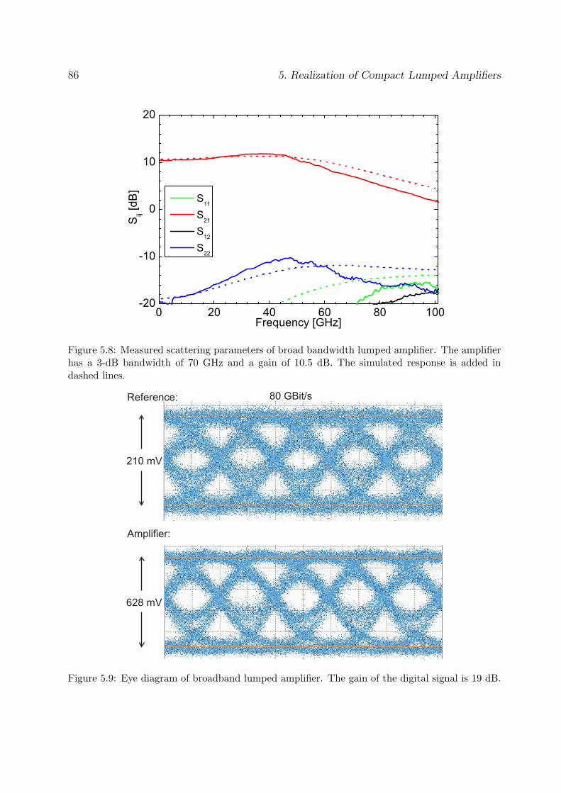
86 5. Realization of Compact Lumped Amplifiers
Figure 5.8: Measured scattering parameters of broad bandwidth lumped amplifier. The amplifierhas a 3-dB bandwidth of 70 GHz and a gain of 10.5 dB. The simulated response is added indashed lines.
Reference:
210 mV
628 mV
80 GBit/s
Amplifier:
Figure 5.9: Eye diagram of broadband lumped amplifier. The gain of the digital signal is 19 dB.

5.3. Output Power Limit 87
The origin of the degraded input eye diagram in comparison to the 40 Gbit/s eye diagramshown above is the limited bandwidth of the measurement setup (s. Sec. 4.3.2). The outputand input eye pattern have comparable shape and the quality of the output pattern is ratherimproved in comparison to the input eye diagram. The signal gain is 9.5 dB and the outputvoltage swing of 628 mV corresponds to an output power of 0 dBm or 1 mW.
Discussion
The results show, that the small-signal models (s. Sec. 3.3) can predict the behavior of thelumped amplifiers quite accurately. A likely reason for differences are parasitic effects whichresult from the wiring within the circuit. Accurate modeling of the short interconnects isdifficult because of coupling between adjacent structures.
The bandwidth of the amplifier is 70 GHz. Still, the transmission of 80 Gbit/s signalsis possible. The relative eye opening of the output eye diagram is slightly improved by theamplifier. Possible explanations for this effect are the gain peaking, which compensatespart of the losses at high frequencies, and the higher output voltage swing, which increasesthe relative accuracy of the measurement system.
The use of only three transistors results in a small chip size, low power consumption,and high yield. All three points are advantages of the realized amplifiers. Consequently,the lumped approach is advisable for the realization of amplifiers for 80 Gbit/s signalsat low output power levels. As will be shown in the next section, the lumped approachis not suitable for realizing high output power amplifiers. However, an application as apre-amplifier for modulator drivers is possible.
5.3 Output Power Limit
This chapter has presented two lumped amplifiers, which can amplify 40 and 80 Gbit/ssignals. Their output voltage swings were about 600 mV. The maximum available outputpower from these amplifiers is investigated in this section.
The limitation in output power can be observed in an eye diagram measurement. Ifthe input signal power level is large enough, the output signal is limited by the maximumavailable output power. The gain drops and the eye diagram shows the limiting behaviorby distorting the signal. This observation is shown in Fig. 5.10. The input signal hasa voltage swing of 468 mV. The eye diagram measurement of the same amplifier fromabove (Sec. 5.2.3) predicts a gain of 9.5 dB, i.e. an output voltage swing of 1.4 V in thiscase. However, the swing of the output signal is limited to 806 mV, which corresponds to again of only 5 dB. The signal is also distorted. This behavior was found for both amplifiersat various input power levels and at data rates of 40 and 80 Gbit/s. The output voltageswing was always limited to about 800 mV (= 2 dBm).
The power limit is due to the small transistors of the amplifier. As explained in Sec-tion 5.1, the amplifier is matched to a 50 Ω environment. A power of 2 dBm correspondsto a current swing of 16 mA. This is twice the bias current of the output transistor Q3

88 5. Realization of Compact Lumped Amplifiers
Reference:
468 mV
806 mV
40 GBit/s
Amplifier:
Figure 5.10: Distorted eye diagram of broad bandwidth lumped amplifier due to limited outputpower at 40 GBit/s.
in Fig. 5.3 and indicates, that the output signal is limited by the available current of theoutput transistor.
The output voltage swing is 804 mV, which is much smaller than the breakdown voltageof the transistors, which is higher than 4 V. Therefore, if the amplifier would be matchedto a higher output impedance, a current swing of 16 mA would cause a higher voltageswing. The output power would increase without changing the transistor size or circuitconcept. For this reason, narrow band power amplifiers use impedance matching networksat the output. A schematic of this concept is shown in Fig. 5.11.
Impedance matching networks cannot be used in broadband amplifiers. Although,these matching networks can increase the output power considerably, they have limitedbandwidth. In order to keep the losses of the matching network to a minimum, reactivecomponents have to be used. However, the efficiency of transmission and the bandwidthare exchangeable quantities in the impedance matching of any load having a reactive com-ponent [76], [32]. Therefore, the use of an impedance matching network to increase theoutput power of the amplifier, would reduce the bandwidth performance, which is not ac-ceptable for amplifiers in high-bit-rate data transmission systems. Such amplifiers have tooperate from frequencies below 1 MHz up to frequencies in the order of the bit rate [87].
As impedance matching networks cannot be used, the output power of the amplifier canonly be increased by increasing the current that is switched by the output stage. There

5.3. Output Power Limit 89
impedance-matchingnetwork
amplifier Z0
Zin
Z0
Figure 5.11: Schematic of an amplifier and an impedance matching network in a circuit envi-ronment with an impedance level Z0. The matching network transforms the impedance of theenvironment to an impedance Zin, which is optimized for maximum power transmission from theamplifier to the environment. Unless the impedance matching network is purely resistive (i.e. verylossy) the network has a limited bandwidth [32].
are two main concepts to achieve this. First, larger transistors can be used. Second, adistributed amplifier can be employed in which several amplifiers operate in parallel.
Using larger transistors has disadvantages. Good matching of the amplifier is moredifficult to achieve, because the input capacitance of the devices and parasitic capacitancesare increased [9]. This has negative consequences for the bandwidth performance. As thelumped broadband amplifier from above has a bandwidth of 70 GHz, a further reductionin bandwidth is not acceptable. Furthermore, the reliability of the circuit suffers, if highpower is dissipated in the very small area of the output device [107]. Therefore, a fullylumped approach for high power driver circuits is not advisable.
To overcome these limitations, distributed amplifiers can be used. Distributed con-cepts do not only yield higher output power, they also allow to increase the bandwidthconsiderably in comparison to lumped amplifiers [8]. The following chapter deals with thedevelopment of distributed amplifiers and demonstrates their advantages with respect tobandwidth and power performance.

90 5. Realization of Compact Lumped Amplifiers

Chapter 6
Distributed Amplifiers for 80 Gbit/s
Distributed amplifiers (DA) achieve larger bandwidth values and more output power thanlumped amplifiers. The lumped approach is mainly limited by the input capacitance andthe parasitic capacitances of the transistors as stated in Section 5.3. Distributed ampli-fiers, on the other hand, turn these capacitances into circuit components neutralizing theirlimiting effect. These amplifiers have input and output artificial lines made up of a se-ries of transmission line sections and the capacitances of the transistors. Because theseartificial lines have a very high cut-off frequency, the amplifiers inherently have widebandcharacteristics. Therefore, the distributed amplifying technique is an excellent way to buildbroadband amplifiers. A schematic of a distributed amplifier is depicted in Fig. 6.1.
In this topology the gain cells couple the signal from the input transmission line to theoutput transmission line through each section. Each gain cell provides amplification of thesignal. Ideally, the traveling wave gets additively superimposed on the output transmissionline at each section as it travels toward the output. The traveling wave concept and itsadvantages are well documented in literature [5],[6],[14],[108].
The fact that several amplifier cells are arranged in parallel, enables distributed am-plifiers to drive high currents. Therefore, higher output power levels can be expected incomparison to a lumped amplifier approach. This second advantage makes the distributedamplifier concept a very attractive candidate for the development of high-bit-rate modu-lator drivers, which depending on the modulator can require voltage swings of more than5 V.
The following sections describe the development of modulator driver concepts for80 Gbit/s applications using InP-HBTs. Section 6.1 gives details about distributed am-plifier design issues. Section 6.2 describes design concepts and presents circuit results forthree generations of distributed amplifiers. The final amplifier version features excellentpower and bandwidth performance. The last section summarizes the key points of thischapter.
91

92 6. Distributed Amplifiers for 80 Gbit/s
RIN
out(VCC)
in(VB)
ROUT
LTL
LTL
LTL
LTL
LTL
LTL
LTL
LP LP LP LP LP
LTL
COUT
CIN
LTL
2
LTL
2
LTL
2
LTL
2
Figure 6.1: Schematic of a 5-cell distributed amplifier.
6.1 Design Considerations
The basis of the distributed amplifier concept are artificial transmission lines. These lineshave cut-off frequencies, electrical delays and impedances, which are characterized by theirinductance L and their capacitance C. The latter consists mostly of the input and outputcapacitances of the gain cells (Fig. 6.1). The cut-off frequency fc, the electical delay T ,and the impedance Z are calculated using [14]:
fc =1
π√
LC(6.1)
T =√
LC (6.2)
Z =
√L
C(6.3)
.The inductance L is usually adjusted to match the impedance Z to the circuit environ-
ment, which has an impedance level of 50 Ω . From these boundary conditions it can becalculated that the cut-off frequency fc will exceed 80 GHz, if the capacitance value C issmaller than 80 fF. In first order approximation the largest contributing to C is the input ca-pacitance of a transistor, which is approximately equal to the capacitance Cje (s. Fig. 3.16).This capacitance was extracted for several transistors and its value is smaller than 80 fF,if the devices have an emitter size of less than 1 × 10 μm2 (s. Fig.3.17). Therefore, thecut-off frequency of the artificial transmission lines are not an issue, if small transistors areused in amplifier design. However, the electrical delay T is of interest as it can be different

6.1. Design Considerations 93
in input and output transmission line due to differences in input and output capacitanceof the gain cells.
Many accounts of the general theory about dimensioning and calculating distributedamplifiers in HEMT as well as HBT technology are given in literature [2],[1],[108]. In thefollowing sections design issues are discussed, that were important for the development ofdistributed amplifiers presented later in this chapter.
6.1.1 Gain Cell Design Concepts
The simplest form of a gain cell consists of a single transistor in common-emitter configu-ration. The high-frequency performance of a such an amplifier cell is limited by the Millercapacitance [61]. The value of this capacitance can be estimated to be the collector-basecapacitance multiplied by the voltage gain of the device, which is typically much larger thanone. It has been shown that the Miller capacitance adds directly to the input capacitanceof the transistor stage degrading its frequency response [37].
To overcome these limitations in the design of distributed amplifiers, two conceptscan be used. First, the devices are scaled down to reduce all capacitance values, in gen-eral [61]. Second, the common-emitter single stage is replaced by two transistors in acommon-emitter common-base configuration called cascode configuration [60], [7]. Theformer concept is followed, naturally, because the devices used in this work are at thelower scaling limit of the present technology (s. Sect. 2.4). The latter concept has beendemonstrated to be an excellent method to achieve high performance distributed ampli-fiers [9], [8]. Fig. 6.2 shows a schematic of a gain cell using the cascode configuration.The cascode derives its advantage at high frequencies from the fact that the collector loadfor the common-emitter stage is the very low input impedance of the common-base stage.This reduces the voltage gain to nearly unity diminishing the Miller effect [37]. Otheradvantages of cascode cells are their very high output impedance, which reduces the lossesin the output transmission line of the distributed amplifier (s. Sect. 6.1.2), and high degreeof isolation from the output to the input.
More sophisticated gain cells have been proposed [4], [62]. These concepts result instate-of-the-art distributed amplifiers. However, they do not show a significant improve-ment in performance over concepts based on simple cascode designs. Disadvantages ofsuch very complex amplifiers include higher power consumption, more dissipated powerand possibly lower yield due to the large number of devices.
In this work the inner core of all gain cells is a cascode configuration. Modified gain cellswith large devices are used to improve the power performance (s. Sect. 6.2.3). Attenuationcompensation techniques are used to enhance their high-frequency performance.
6.1.2 Attenuation Compensation
Without loss compensation techniques distributed amplifiers cannot achieve their maxi-mum wideband characteristic. The artificial transmission lines of a distributed amplifierhave losses which are mainly attributed to the limited input and output impedance of

94 6. Distributed Amplifiers for 80 Gbit/s
OUT (VCC)
IN (VB)
Q1
Q2
RED CED
RD
RFB
RBIAS CHF
Figure 6.2: Gain cell of first distributed amplifier version employing a cascode configura-tion (Q1, Q2), self-biasing (RFB, RBIAS), and emitter degeneration (RED, CED).
the gain cells. These losses are particularly high at high frequencies. Attenuation com-pensation techniques can be used to increase the gain-bandwidth product of a distributedamplifier [26]. For the development of broad-bandwidth and high-gain amplifiers the im-plementation of such techniques is mandatory. This section gives an overview of mostcommon techniques.
Cascode Configuration
Cascodes feature a higher output impedance than single-transistor common-emitter con-figurations [37]. Hence, the implementation of cascode configurations reduces the losses inthe output transmission line [58]. A distributed amplifier using cascodes can employ morecells, which results in higher gain. In this case, the losses of the input transmission linedominate.
Emitter Degeneration
Attenuation compensation can be achieved using a resistive emitter degeneration at thecommon-emitter transistor of the cascode configuration. The input impedance is increasedand the resistive loading of the input line is reduced [87]. The emitter resistance is alsoused to control the gain of the amplifier.
The emitter degeneration can be extended by a parallel capacitance (CED in Fig. 6.2).This capacitance causes peaking at high frequencies and can compensate the attenuationof the transmission lines. This technique is particularly useful for extending bandwidth [7].

6.1. Design Considerations 95
OUT (VCC)
IN (VB)
VE
Q1
Q2
Q3
CHF2
RED
RD
REF1
CHF1
VC
Figure 6.3: Gain cell of second amplifier version employing a cascode configuration (Q1, Q2),emitter degeneration (RED), and an emitter follower (Q3).
Emitter Followers
Emitter followers at the input of a gain cell alleviate two limiting factors. The first limitin HBT distributed amplifiers is the input capacitance of the common emitter device,which creates the dominant cut-off pole for high-frequency response [61]. This high inputcapacitance in comparison to HEMTs is due to the close proximity of the base to theactive conduction region when viewed as a charge controlled device [50]. Second, the inputimpedance of HBTs is low even if emitter degeneration is used and causes high losses inthe input transmission line.
A gain cell using emitter follower buffering is shown in Fig. 6.3. The input impedanceis increased as the emitter resistance of Q3 is larger than emitter resistance of Q1. Athigh frequencies the emitter follower device actively transforms the capacitive impedanceat the emitter and generates a negative resistance at its base [58]. The combination ofboth effects results in lower losses in the input transmission line and increases bandwidth.
Capacitive Division
Capacitive division is a technique, which introduces a series capacitance at the input ofeach gain cell. It increases the input impedance of the gain cell and reduces its inputcapacitance [84], [5]. The former effect reduces the losses of the input transmission lineand the latter effect increases the bandwidth performance of the amplifier. Very broadbandwidth HBT distributed amplifiers have been demonstrated [1]. However, capacitivedivision has significant disadvantages.
First, capacitive division reduces gain, as the input signal is divided between the seriescapacitor and the base node of the input transistor [53]. Second, due to practical geo-metrical considerations the series capacitor value is limited to a few pF. This results in

96 6. Distributed Amplifiers for 80 Gbit/s
a deteriorated low-frequency behavior of the amplifier [1]. However, for the transmissionof digital signals, constant gain performance down to frequencies as low as a 800 kHz for80 GBit/s are desirable [2]. Simulations show, that capacitance values of 50 pF and largerwould be necessary to achieve acceptable low-frequency performance. Therefore, capacitivedivision was not used in the development of driver amplifiers.
Peaking Lines
This attenuation compensation technique employs transmission lines between the elementsof the gain cell or at its output. They transform the impedance between the elementsconnected. A detailed analysis of peaking lines reveals that the performance of distributedamplifiers using cascode gain cells can be improved significantly [53], [52]. In particular, atransmission line extending the output of the gain cell (LP in Fig. 6.1) can contribute toexcellent broad-bandwidth performance [7]. If used correctly, the output capacitance of thegain cells can be matched to the input capacitance of the gain cells, which is important formatching the electrical delays in input and output transmission line (s. Equ. 6.2). Also, thelosses of the output transmission line can be compensated by high-frequency gain peaking.Finally, this attenuation compensation technique can also control the roll-off characteristicof the amplifier.
6.1.3 Coplanar and Microstrip Transmission Lines
Three different transmission line technologies for the realization of distributed amplifierscan be found in literature. First, microstrip lines (MSL), which use a metalization at thebackside of the substrate as the ground plane. Second, inverted microstrip lines (IMSL),which use a metal layer on top of the wafer separated from the circuit by a dielectricas ground. Third, coplanar waveguides (CPW), with a ground-to-ground spacing of usu-ally 50 μm.
IMSLs show little frequency dispersion and will avoid proximity effects, if chips areflip-chip bonded. High performance DAs have been demonstrated using this approach [75].MSLs cannot confine the electric field in a small region. Substrates typically have a thick-ness of several hundred micrometer and the electric field spreads out laterally approximatelythe same distance. This can cause coupling between adjacent structures. Moreover, MSLsshow a significant amount of frequency dispersion. Therefore, MSLs are not a good choicefor the realization of distributed amplifiers.
CPWs show lower dispersion, lower coupling and require less chip area than MSLs. Adrawback are higher conductor losses. However, in HBT DAs losses due to the transistordevices dominate the losses of the distributed transmission line network [59]. These lossescan be compensated by using attenuation compensation techniques (s. Sect. 6.1.2). Hence,CPWs are well suited for DA design and were used in this work. A distributed amplifierlayout using CPWs is shown in Fig. 6.4.

6.1. Design Considerations 97
Figure 6.4: Photograph of a five-cell distributed amplifier. The chip size is 640 × 1340 μm2.
6.1.4 Transmission Line Termination
The artificial transmission lines of distributed amplifiers have to be terminated in orderto prevent reflections. Reflections would lead to pronounced gain variations over the fre-quency band and degrade matching of input and output port. A straightforward methodof termination is a series combination of a resistance matching the effective impedance ofthe artificial transmission line and a large capacitance (s. Fig. 6.1). The capacitor preventsunwanted power dissipation in RIN and ROUT , when the circuit is biased. The capacitancevalue has to be large enough to secure acceptable low-frequency performance (s. Sect. 6.1.2).In cases where this is not possible due to limited available chip area, three alternative con-cepts can be used to extend the low-frequency performance of distributed amplifiers: activeloads [60], off-chip capacitors, or direct DC-matching terminations.
Active loads transform the on-chip capacitance into a larger value using a small networkof a transistor and resistors. It has been shown, that this concept can result in distributedamplifiers with excellent low-frequency performance [57]. Simulations confirmed that theactive load concept can improve the low-frequency performance of a distributed amplifierfor a given on-chip capacitance value. However, the investigation also revealed that activeloads reduce the bandwidth performance. The impedance transformation is frequencydependent and degrades matching of the terminations at very high frequencies and, hence,limits the bandwidth.
Instead of using active loads, large value off-chip discrete capacitors can be integratedto extend the low-frequency response. However, the integration of off-chip capacitors cancause problems. Often these discrete capacitors have self-resonances which fall within thepassband of the amplifier [60]. The problem may be compounded by the effects of wirebondparasitics in combination with the discrete capacitor component [7]. These effects cansometimes result in in-band resonances and gain ripples due to standing waves in either ofthe input or output distributed transmission lines and are cumbersome to manage.
DC-matching termination, leaving out the capacitor, can be used to obtain flat gain

98 6. Distributed Amplifiers for 80 Gbit/s
from frequencies as low as 0 Hz [53]. The drawback of this simple design is the increasedpower consumption caused by the bias voltage in the transmission line. Also, the circuitcannot be biased through the termination requiring the implementation of bias-Ts at theinput and output of the circuit.
6.1.5 Linear and Matrix Design
Distributed amplifiers can follow linear or matrix concepts. A linear concept featurestwo artificial transmission lines for the input and the ouput connected by a row of gaincells (s. Fig. 6.1). This is the most widely used concept. Matrix amplifiers consist of twoor more rows of gain cells. The output transmission line of a lower row serves as inputtransmission line for the upper row. This results in a layout where gain cells are arrangedlike elements in a matrix.
Matrix amplifiers offer more flexibility in using device scaling and capacitive couplingtechniques [61]. However, there is no indication that a matrix amplifier has a betterperformance than a cascade of several linear amplifiers with the same total number of gaincells. An experimental comparison between a two-row matrix distributed amplifier and adual-stage linear distributed amplifier did not show any advantage of either concept overthe other [25]. Recently, half-matrix half-dual-stage distributed amplifier concepts havebeen reported without demonstrating significant advantages [56]. If complex concepts donot lead to improved circuit performance, they should not be implemented. It would leadto higher power consumption and lower yield, i.e. higher costs. Consequently, this workdeals with the development of linear distributed amplifiers.
6.1.6 Single-ended and Differential Design
Distributed modulator driver amplifiers can be designed for differential or single-endedinput and output. An advantage of differential designs is, that the voltage output swingcan be considerably larger than in a single-ended design. Also, multiplexers usually have adifferential output, because differential multiplexer designs reach higher speed than single-ended concepts. For 40 GBit/s excellent modulator driver performance using differentialdesigns has been demonstrated [110], [9].
Differential amplifiers usually consist of two single-ended amplifiers, which are coupledat each gain cell. In first order approximation the performance of the differential amplifieris determined by the single-ended design concept. Therefore, an evaluation of modulatordriver concepts can be conducted using the single-ended approach. The lower complex-ity results in higher yield and shorter design cycles during the development. This workconcentrates on the optimization of single-ended amplifiers.

6.2. Realized Amplifiers 99
Figure 6.5: Measured scattering parameters (solid lines) of distributed amplifier using resistivefeedback. The gain is 10 dB and the 3-dB bandwidth is 102 GHz. The simulated response isadded in dashed lines.
6.2 Realized Amplifiers
In this section three distributed amplifiers are presented, corresponding to three majordevelopment steps toward the realization of high-power modulator drivers for 80 GBit/s.First, a low-power very broad bandwidth amplifier is shown. Second, a more sophisti-cated amplifier removes some deficiencies of the previous version and introduces a losscompensation technique. Third, an amplifier optimized for high output power operation ispresented. All amplifiers are characterized using scattering parameter, eye diagram, andpower measurements.
6.2.1 Low-Power 100 GHz Bandwidth Amplifier
The design goal of the first version was simplicity and demonstration of the technology’spotential, i.e. bandwidth. A low number of devices results in high yield. A direct compar-ison to the lumped amplifiers in Chapter 5 can be made.
Design and Layout
The gain cell of this amplifier is shown in Fig. 6.2 and uses transistors with an emittersize of 1 × 4 μm2. It features a cascode configuration, whose advantages were describedin Sects. 6.1.1 and 6.1.2. Although the cascode configuration improves the output resistanceand bandwidth performance, it tends to be unstable for HBTs [58]. To ensure stability the
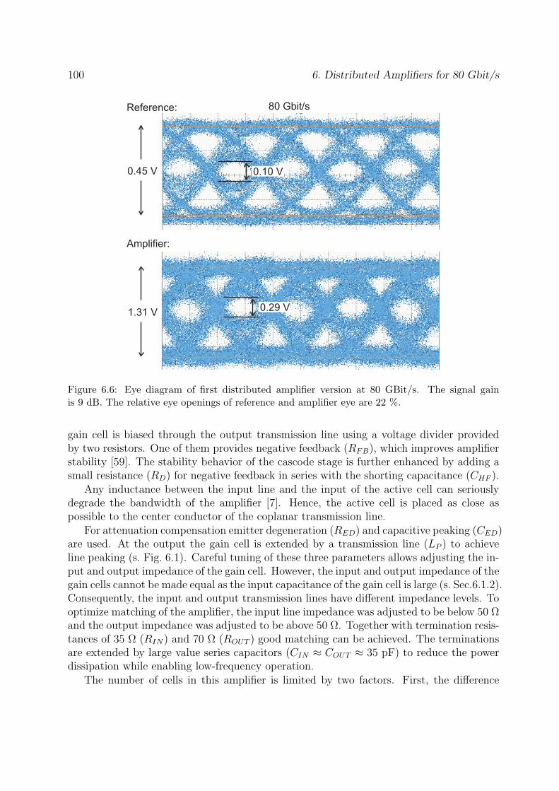
100 6. Distributed Amplifiers for 80 Gbit/s
Reference:
0.45 V
0.29 V
0.10 V
1.31 V
80 Gbit/s
Amplifier:
Figure 6.6: Eye diagram of first distributed amplifier version at 80 GBit/s. The signal gainis 9 dB. The relative eye openings of reference and amplifier eye are 22 %.
gain cell is biased through the output transmission line using a voltage divider providedby two resistors. One of them provides negative feedback (RFB), which improves amplifierstability [59]. The stability behavior of the cascode stage is further enhanced by adding asmall resistance (RD) for negative feedback in series with the shorting capacitance (CHF ).
Any inductance between the input line and the input of the active cell can seriouslydegrade the bandwidth of the amplifier [7]. Hence, the active cell is placed as close aspossible to the center conductor of the coplanar transmission line.
For attenuation compensation emitter degeneration (RED) and capacitive peaking (CED)are used. At the output the gain cell is extended by a transmission line (LP ) to achieveline peaking (s. Fig. 6.1). Careful tuning of these three parameters allows adjusting the in-put and output impedance of the gain cell. However, the input and output impedance of thegain cells cannot be made equal as the input capacitance of the gain cell is large (s. Sec.6.1.2).Consequently, the input and output transmission lines have different impedance levels. Tooptimize matching of the amplifier, the input line impedance was adjusted to be below 50 Ωand the output impedance was adjusted to be above 50 Ω. Together with termination resis-tances of 35 Ω (RIN) and 70 Ω (ROUT ) good matching can be achieved. The terminationsare extended by large value series capacitors (CIN ≈ COUT ≈ 35 pF) to reduce the powerdissipation while enabling low-frequency operation.
The number of cells in this amplifier is limited by two factors. First, the difference

6.2. Realized Amplifiers 101
Figure 6.7: Output power at 1-dB compression point and gain of distributed amplifier employingresistive feedback. The discontinuity at 50 GHz is due to the measurement system (s. Sec. 4.3.1).
in impedance level results in different electrical delays in input and output transmissionlines (Eq. 6.2). Hence, the electrical signals of each gain cell, which are superimposed inthe output transmission line, are not exactly in phase. If the lines are too long, the effectdegrades the bandwidth. Second, the low input impedance of the gain cells attenuates theinput signal, significantly. If the number of cells is too high, the signal at the last cellwill be too low for the gain cell to contribute a noticeable amount of gain. Still, this gaincell would cause finite losses in the output line reducing the gain of the amplifier. If thenumber of cells is too low, the gain will be lower than necessary. According to simulationsa five-cell amplifier as shown in Fig. 6.1 is a good compromise. A chip photograph of theamplifier is shown in Fig. 6.4.
Results
The amplifier was measured with a power supply of 3.5 V (VCC) and 1.0 V (VB). Thebias current was 43 mA resulting in a power consumption of approximately 150 mW. Thiscorresponds to a current density of 1.9 × 10⁵ A/cm2 in each transistor.
The bandwidth performance is shown in Fig. 6.5. The small-signal gain is 10 dBand the 3-dB bandwidth is 102 GHz. The input matching is better than −13 dB overthe full bandwidth and the output matching is better than −10 dB up to 85 GHz. Thesimulated data are also shown in dashed lines in Fig. 6.5. The oscillations in the measuredamplifier response beyond 80 GHz are attributed to excessive peaking. Capacitive peakingenhances the bandwidth, but it is very sensitive. Because a slight reduction in bandwidth

102 6. Distributed Amplifiers for 80 Gbit/s
Figure 6.8: Output power vs. input available power and gain of distributed amplifier employingresistive feedback measured at a frequency of 60 GHz. The 1-dB compression point is at 8 dBmoutput power.
is acceptable for the transmission of 80 Gbit/s data signals, this peaking technique is notused in the amplifiers presented in the following Sections.
An eye diagram measurement is presented in Fig. 6.6. The input eye is already degradeddue to bandwidth limitations in the measurement setup (s. Sec. 4.3.2). The output eye isslightly degraded in comparison to the input eye. Still, the relative eye openings of boththe input and output eyes are 22 %. The signal gain is 9 dB. The output eye does notshow any limiting effect, which indicates that the amplifier can support larger signals. Inorder to estimate this maximum output swing, power measurements were conducted.
A power and large-signal gain measurement is depicted in Fig. 6.7. The graph showsthe output power at 1-dB compression point. The slight discontinuity at 50 GHz isdue to different measurement setups for the frequency bands above and below this fre-quency (s. Sec. 4.3.1). The output power starts at 9 dBm for low frequencies and graduallydecreases to 6 dBm at 75 GHz. The large-signal gain is 10 dB and matches the small-signal gain in Fig. 6.5. Fig. 6.8 shows a power sweep of the amplifier at 60 GHz. The1-dB compression point is reached at an output power of almost 8 dBm, which corre-sponds to a peak-to-peak voltage swing of 1.6 V. The results of the power measurementindicate, that the maximum voltage swing of the amplifier for an 80 GBit/s signal is be-tween 1.3 V (= 6 dBm) and 1.8 V (= 9 dBm).

6.2. Realized Amplifiers 103
Figure 6.9: Photograph of second amplifier version using emitter followers and external bias ports.The chip size is 900 × 1860 μm2.
Discussion
This first distributed amplifier version clearly demonstrates the advantages of the dis-tributed concept. Due to the lower operating voltage the power consumption of thisamplifier is comparable to the lumped amplifiers presented in Chapter 5. However, thebandwidth is 45 % larger than in the case of the lumped amplifier while reaching the samegain. The maximum output swing is 60 % larger. The following versions of distributedamplifiers modify the concept to enhance gain and power performance while maintaininga bandwidth that supports the amplification of 80 GBit/s signals.
6.2.2 Tunable Amplifier for Loss Compensation
While the first distributed amplifier version achieved remarkable results using basic designprinciples, it lacks features that are necessary for modulator drivers. The number of cellsis limited, resulting in a limitation of gain and output power. Both figures of merit are im-proved in this second version by using attenuation compensation techniques in combinationwith a larger number of cells.
Design and Layout
The gain cell of this amplifier uses transistors with an emitter size of 1 × 4 μm2 and em-ploys an emitter follower at its input (Fig. 6.3). This results in positive consequences.The resistive loading as well as the capacitive loading of the input transmission line arereduced (s. Sec. 6.1.2). Lower resistive loading lessens the attenuation in the input trans-mission line. The input signal after the fifth cell is still strong enough for utilizing additionalgain cells. This adds to the amplifier gain. According to simulations a total number ofeight cells can be used. For simulations a small-signal model was used.

104 6. Distributed Amplifiers for 80 Gbit/s
Figure 6.10: Scattering parameters of tunable distributed amplifier. Solid lines: response atoperating point for flat gain and small-signal gain at operating point for eye diagram and powermeasurements. Dashed line: Simulated response for flat gain.
The lower input capacitance makes it possible to match the input and output capaci-tance of the gain cells. In contrast to the previous amplifier version the impedance of theartificial input and output transmission lines can be made equal and matched to the 50 Ωcircuit environment. This leads to significant improvement in the matching of amplifierinput and output. Furthermore, the electrical delays in input and output transmission lineare equal (Eq. 6.2), which ensures that the gain cell output signals are in phase.
Line peaking and emitter degeneration as additional attenuation compensation tech-niques are used. These techniques were employed in first amplifier version, too. However,capacitive peaking is not used for two reasons. First, capacitive peaking often leads to asteep roll off, which can cause signal distortions at very high bit rates. For data transmissionsystems it is advisable to trade a certain amount of bandwidth for a gradual roll off [8].Second, this amplifier does not use negative feedback at the cascode (RFB in Fig. 6.2)which makes the amplifier more sensitive to oscillations. Reducing the number of peakingmechanisms alleviates this problem.
Negative feedback at the cascode is not used, because the amplifier has external biasports for the base of transistor Q2 (Fig. 6.3). The additional external bias port can beused to compensate minor deficiencies in design or technology to a certain degree. Thebias conditions of Q1 and Q2 can be set independently allowing to alter the frequencycharacteristic of the amplifier. A chip photograph of the amplifier is depicted in Fig. 6.9.

6.2. Realized Amplifiers 105
Reference:
0.45 V
1.50 V
80 Gbit/s
Amplifier:
0.10 V
0.51 V
Figure 6.11: Eye diagram of second distributed amplifier version at 80 GBit/s. The gain ofthe signal is 10.5 dB. The relative eye openings of input and output eye are 22 % and 34 %,respectively.
Results
The amplifier was measured in two different operating conditions. First, it was biasedfor flat small-signal gain. Second, a bias point was chosen, which optimizes the shapeand height of the eye diagram and maximizes the output power. The bias conditions andcorresponding power consumptions are given in Table 6.1. The values correspond to acurrent density of 1.9...2.4 × 105 A/cm2 in each transistor.
Measured scattering parameters of this amplifier are shown in Fig. 6.10. If operated in
condition VCC (V) ICC (mA) VC (V) IC (mA)flat gain 3.8 59 2.0 ≈ 1
max. power 4.2 78 2.6 ≈ 1
condition VE (V) IE (mA) VB (V) IB (mA) P (mW)flat gain 2.4 67 2.1 ≈ 1 420
max. power 3.0 71 2.2 ≈ 1 540
Table 6.1: Bias conditions and power consumption for flat gain and maximum output powercondition of distributed amplifier with one emitter follower in each gain cell.

106 6. Distributed Amplifiers for 80 Gbit/s
flat gain condition, the small-signal gain is 11 dB and the 3-dB bandwidth is 82 GHz. Theroll off is very gradual. The matching of the input and output is better than −10 dB overthe full bandwidth. The small-signal gain for eye and power measurement is shown also.In this operating condition the gain increases to higher frequencies and starts to oscillateabove 80 GHz. The simulated response for flat gain is shown in dashed lines. The reducedbandwidth in the measurement is attributed to a fact, that the peaking mechanisms aretoo weak. In comparison to the previous amplifier, which exhibited too much peaking, thisamplifier rather uses too little.
The result of an 80 GBit/s eye diagram measurement is depicted in Fig. 6.11. Theoutput swing is 1.5 V and is limited by the available input swing of the measurementsystem. The gain of the digital signal is 10.5 dB. The output eye is clearer and the eyeopening is larger than in the case of the input eye. The relative eye opening has improvedfrom 22 % for the reference signal to 34 % for the amplifier output signal.
Power measurements were conducted to investigate the maximum output power of thisamplifier. Fig. 6.12 shows the output power against input power at a frequency of 60 GHz.For low and medium output power levels the gain is constant at 17 dB and the amplifierbehavior is linear. The border of the linear region is the 1-dB compression point, wherethe gain has decreased by 1 dB. The output power at this point is 13 dBm. Fig. 6.13summarizes the result of this measurement over a frequency range from 5 to 75 GHz.The output power at 1-dB compression is almost constant at 14.5 dBm up to 40 GHz. At75 GHz the output power has moderately decreased to 12 dBm. The large-signal gain ofthe power measurement corresponds to the small-signal gain of the scattering parametermeasurement (Fig. 6.10).
Discussion
The scattering parameters demonstrate improvements in comparison to the first DA ver-sion. The matching of the amplifier is excellent. This is due to the adjustment of theimpedance in the artificial input and output transmission lines, which was enabled by theuse of an emitter follower in each gain cell. The gain could also be increased by 1 dBat low frequencies and it gradually rises up to 70 GHz by 2 dB. This behavior is calledpre-emphasis and is useful for compensating losses, that get introduced, when the chipis packaged. These losses rise with frequency. The bandwidth performance is reduced.However, the bandwidth still exceeds 80 GHz and the roll off is very gradual, which is ofadvantage for digital signal transmission.
The output eye diagram opening is much larger and clearer, and the amplitude is slightlyhigher than in the case of the previous amplifier. The increase in amplitude correspondsto the increase in small-signal gain. The improved eye opening can be attributed to thegain peaking in the operating point of the eye measurement (s. Fig 6.10). As explainedin section 4.3.2, the setup for the eye diagram measurement is bandwidth limited with anominal bandwidth of 60 GHz. Higher frequencies get attenuated significantly. Apparently,gain peaking can compensate these losses producing a clearer eye opening in comparisonto the reference signal.

6.2. Realized Amplifiers 107
Figure 6.12: Output power against available power at 60 GHz of second DA version. The outputpower at 1-dB compression point is 13.5 dBm.
Figure 6.13: Output power at 1-dB compression point and gain of second DA version.

108 6. Distributed Amplifiers for 80 Gbit/s
The output power capability of this amplifier has been improved by 5 dB over thefull bandwidth with a very gradual decrease of only 2.5 dB from 5 to 75 GHz. Thiscorresponds to an increase in voltage output swing of 80 %. From the results of the outputpower measurement it can be concluded that the maximum peak-to-peak voltage swing ofan 80 GBit/s signal would have a value between 2.6 V (= 12 dBm) and 3.4 V (= 14.5 dBm).
Besides the performance improvements a striking feature of this amplifier concept is thetuning capability. As demonstrated it can be used to adjust the high-frequency performanceto compensate system limitations. An unavoidable drawback of this design is higher powerconsumption due to the larger number of devices used and a larger chip size. Both canlead to a lower yield. The last amplifier version described in the following section takesanother step toward higher output power while maintaining bandwidth.
6.2.3 High-Power Amplifier for 80 Gbit/s
The previous amplifier has shown an excellent performance regarding the amplificationof 80 Gbit/s digital signals. For modulator driver applications higher output power is stilldesirable. Therefore, the last development step focuses on achieving more output powerwithout sacrificing advances of previous development steps.
Design and Layout
The breakdown voltage of the InP-HBTs is high and the expectations regarding powerperformance are not met by the power performance of amplifiers presented in the last twosections. An advancement in circuit design is needed to exploit the potential of the devices.In narrow bandwidth amplifiers a matching network can be used to transform the 50 Ω cir-cuit environment into a load which extracts the maximum power out of a device for a givenoperating point. However, these matching networks have a very limited bandwidth andcannot be used in broadband amplifiers necessary for high-bit-rate application (s. Sect.5.3).
Peaking lines at the output of the gain cells of distributed amplifiers transform theimpedance, but their purpose is to cause peaking at high frequencies and not to improvethe power performance. At lower frequencies impedance transformation by line peaking isnegligible. Therefore, in first order approximation the load for the output device of eachgain cell is 50 Ω.
The signal in the output transmission line gets stronger as it travels toward the amplifieroutput, and, consequently, the stress on the output transistor of the last gain cell is largest.The voltage swing at this device is approximately equal to the amplifier output voltageswing. Hence, the output power of the amplifier is limited by the output current unlessthe voltage swing reaches the breakdown voltage of the devices.
The output driving current in this design is increased by using larger transistors. Inprevious circuits the emitter area of all devices was 4 × 1 μm2. By using a device of twicethe size the output current of the amplifier can be doubled promising higher output powerand more gain, if the number of cells is not changed.

6.2. Realized Amplifiers 109
OUT (VCC)
IN (VB)
VE
Q1
Q2
Q3
Q4
CHF2
RED
RD
REF1REF2
CHF1
VC
Figure 6.14: Schematic of gain cell optimized for maximum output power. The cascode de-vices (Q1, Q2) have an emitter size of 8 × 1 μm2. Emitter followers (Q3, Q4) and diode have anemitter size of 4 × 1 μm2.
A schematic of the gain cell of this new amplifier is shown in Fig. 6.14. The cas-code (Q1, Q2) consists of transistors with an emitter size of 8 × 1 μm2. The implementa-tion of larger transistors increases the input capacitance and reduces the input resistanceof the cascode stage considerably. To compensate this, more attenuation compensation isneeded and two emitter followers (Q3, Q4) with the standard transistor size of 4 × 1 μm2
are implemented. To ensure equivalent bias conditions for Q3 and Q4 a diode is insertedat the collector port of Q3. As a result the loading of the input transmission line is lowenough to design a distributed amplifier with eight cells.
The large cascode devices also cause an increase in output capacitance. This increasecan be compensated partly by adjusting the attenuation compensation mechanism of thepeaking line LP (s. Fig. 6.1). However, the input capacitance and output capacitance ofthe gain cells cannot be made equal. This leads to different impedance levels in input andoutput artificial transmission lines of the distributed amplifier. As discussed before thematching of the amplifier can be degraded and different electrical delays in the input andoutput line can degrade the gain performance at high frequencies. However, simulationsshow, that this degradation is acceptable. It is the price for achieving higher output powerlevels, while keeping amplifier concepts as simple as possible.
As before, external ports for biasing the emitter followers and the base of the cascodeare provided allowing the compensation of design errors and process variations to a certaindegree. Shorting capacitances (CHF1 and CHF2 in Fig. 6.14) are provided to optimize thehigh-frequency performance. The design and layout concepts of the artificial transmission

110 6. Distributed Amplifiers for 80 Gbit/s
Figure 6.15: Photograph of final distributed amplifier version optimized for output power. Thechip size is 900 × 2280 μm2.
lines and terminations are identical to the previous amplifier versions. A total of 40 devicesis used in this amplifier. A chip photograph of the distributed amplifier is given in Fig. 6.15.
Results
The amplifier was measured in different operating conditions. For maximum bandwidthit was biased at moderate voltages and currents. For maximum output power the de-vices in the amplifier were put under more stress. The bias conditions and correspondingpower consumptions are given in Table 6.2. The values correspond to a current densityof 1.8...2.7 × 105 A/cm2 in each transistor.
Measured scattering parameters are shown in Fig. 6.16. If the amplifier is biased forlarge bandwidth and moderate peaking, the gain is 12 dB with a peaking of 3 dB and abandwidth of 94 GHz. The matching of the input and output is better than −10 dB upto 75 GHz and over the full bandwidth, respectively. The amplifier response displays ripplesin the gain for frequencies above 80 GHz. The roll-off is fairly steep. The small-signal gainat other operating points is added, too. Dashed lines show the simulated amplifier response
condition VCC (V) ICC (mA) VC (V) IC (mA)max. bandwidth 3.8 121 2.2 ≈ 1
eye diagram 4.0 131 2.4 ≈ 1max. power 4.5 175 2.5 ≈ 1
condition VE (V) IE (mA) VB (V) IB (mA) P (mW)max. bandwidth 3.3 117 2.8 ≈ 1 850
eye diagram 3.6 137 2.9 ≈ 1 1020max. power 3.9 165 3.0 ≈ 1 1430
Table 6.2: Bias conditions and power consumption for maximum bandwidth, eye diagram mea-surement, and maximum output power condition of 8-cell distributed amplifier with two emitterfollowers and large area cascode devices (s. Fig. 6.14).

6.2. Realized Amplifiers 111
Figure 6.16: Scattering parameters of high-gain distributed amplifier. Solid lines: response atoperating point for maximum bandwidth and small-signal gain at operating points for eye diagramand power measurements. Dashed lines: Simulated response for maximum bandwidth condition.
for flat gain condition.
The result of an 80 GBit/s eye diagram measurement is depicted in Fig. 6.17. Theoutput swing is 2.4 V and is limited by the available input swing of the measurementsystem. The gain for the digital signal is 14.5 dB. The output eye is clearer and the eyeopening is much larger in comparison to the input eye. The relative eye opening of theoutput eye is 44 % in comparison to 22 % for the reference signal. The optimum eye shapewas achieved using the tuning capability of the amplifier. The small-signal gain that relatesto the eye diagram measurement condition is given in Fig. 6.16.
Power measurements were conducted to investigate the maximum output power of thisamplifier. Fig. 6.18 shows the output power against input power at a frequency of 60 GHz.For low and medium output power levels the gain is almost constant around 24 dB and theamplifier behavior is linear. The 1-dB compression point is reached at an output power levelof 15.5 dBm. Fig. 6.19 summarizes the output power performance over a frequency rangefrom 5 to 75 GHz. The output power at 1-dB compression is almost constant at 18 dBmup to 40 GHz and decreases less than 3 dB up to 60 GHz. Above this frequency theoutput power roles off faster to 10.5 dBm at 75 GHz. The large-signal gain of the powermeasurement corresponds to the small-signal gain in the same operating point (Fig. 6.16).

112 6. Distributed Amplifiers for 80 Gbit/s
Reference:
0.45 V
2.38 V
80 Gbit/s
Amplifier:
0.10 V
1.05 V
Figure 6.17: Eye diagram of distributed amplifier optimized for maximum output powerat 80 GBit/s. The gain of the signal is 14.5 dB. The relative eye openings of reference andamplifier output eye are 22 % and 44 %, respectively.
Discussion
The amplifier’s performance meets the expectations. The gain performance exceeds theprevious versions and the bandwidth is still larger than 80 GHz. The amplifier tends tooscillate at very high frequencies because excessive peaking had to be used to compensatethe change in transistor size. The matching behavior is also degenerated at high frequenciesdue to this change, but it is still acceptable. However, up to 80 GHz the performance ofthe amplifier is excellent.
This statement is confirmed by the eye diagram measurement at 80 GBit/s. In compar-ison to the reference eye the output eye is not only large but also very clear and the openingof the eyes has improved, dramatically. Similar to the previous amplifier version, this isachieved by compensating losses in the measurement system with pronounced peaking ofthe amplifier. The output eye does not show any limiting effects which strongly suggeststhat the maximum available output swing could be considerably larger, if a larger inputsignal would be available.
The power measurements indicate that the maximum output swing at 80 GBit/s isbetween 2.6 V (= 12 dBm) and 5.1 V (= 18 dBm) with a gain of more than 14 dB. Thepower spectrum of an 80 GBit/s digital signal gradually decreases from its maximum at

6.2. Realized Amplifiers 113
Figure 6.18: Output power against input power of final amplifier version at 60 GHz. At 1-dBcompression point the output power is 15.5 dBm.
Figure 6.19: Output power at 1-dB compression point and gain of distributed amplifier optimizedfor maximum output power.

114 6. Distributed Amplifiers for 80 Gbit/s
0 Hz to zero at 80 GHz. Hence, the probability is high that a voltage swing can be achieved,that is closer to the upper than to the lower boundary.
The tuning capability of the amplifier is a very useful feature of this amplifier concept.It cannot only be used to optimize the amplifier’s performance, but also to compensatelosses and deficiencies in other parts of the transmission system. These losses can resultfrom packaging of chips, using bandwidth limited interconnections, or from poor perfor-mance of other circuits. These losses typically increase with frequency. How effectivelygain peaking can compensate such limitations is demonstrated by the eye diagram mea-surement (Fig. 6.17).
In summary, the results show, that the gain cell of this amplifier (Fig. 6.14) and thedesign and layout concept are well suited for realizing modulator drivers at 80 GBit/sat possibly beyond. If this concept is transfered into a differential design voltage swingsexceeding 5 V are conceivable.
6.3 Summary
This chapter described the development of modulator driver concepts for high bit rate op-tical data transmission systems. After a theoretical introduction into distributed amplifierconcepts, a first version of such an amplifier demonstrated the usefulness of this concept byreaching 102 GHz 3-dB bandwidth and 10 dB gain. Although the power consumption andgain were comparable to the lumped amplifiers, the distributed amplifier already reached45 % more bandwidth and 60 % higher output voltage swing.
Using additional attenuation compensation techniques, the second amplifier versionfurther increased gain and output power, while eliminating some deficiencies of the firstamplifier version. This amplifier shows excellent matching, very smooth gain, and goodpower behavior, which would make it suitable for sensitive applications.
Focusing on maximum output power performance, a third amplifier version was realized,which implements transistors of different sizes. This amplifier shows a clear eye diagramat 80 Gbit/s with a voltage swing of 2.4 V and 14.5 dB gain. The voltage swing was limitedby the limited power of the digital input signal. As power measurements show voltageswings of 5 V up to 40 GHz with a reasonable roll off to higher frequencies, considerablylarger eye diagrams than measured seem possible.
The tuning capability is a useful feature of the last two amplifier versions. It can beused to compensate for losses introduced by other parts of a transmission system. Theselosses typically increase with frequency and can result from chip packaging, or the useof bandwidth limited components. How effectively gain peaking can compensate suchlimitations is demonstrated by the eye measurement (Fig. 6.17).
In summary, the results show, that the design and layout concept of the third distributedamplifier version is well suited for realizing modulator drivers at 80 Gbit/s.

Chapter 7
Conclusion and Outlook
Conclusion
The goal of this thesis was the development of broadband amplifiers suitable for ETDMdata transmission systems operating at data rates of 80 Gbit/s and beyond. Especially, themodulator driver posed a challenge, because it does not only have to provide a bandwidthof at least 80 GHz but also an output voltage swing of at least 3 V peak-to-peak. The goalhas been successfully achieved by having conducted the following development steps:
First, the vertical dimensions of InP DHBTs, i.e., the epitaxial layer structure, wasanalyzed using dc and hf measurements and subsequently optimized within two itera-tions. Second, the lateral dimensions, i.e., the transistor layout, was systematically in-vestigated. Critical transistor design issues were identified, experimentally confirmed, andthe device layout was optimized. As a result, state-of-the-art transistor devices featuringhigh-frequency parameters fT and fmax of more than 280 GHz and a breakdown voltageexceeding 4 V were achieved. At the same time, the optimized transistors show a highyield in the present technology, which allows the realization of complex circuits using morethan 100 devices.
Third, from a variety of modeling approaches, the most suitable one was adopted. Anexisting preliminary model extraction procedure was refined and optimized with respectto the demands of the project by making a compromise between accuracy and complexity.This resulted in transistor models which were equally suited for analog as well as digitalcircuit design.
Up to this point, the achievements did not only enable the development of amplifiers,but they also significantly contributed to the successful development of digital circuits for80 Gbit/s, like frequency divider, multiplexer, demultiplexer, and clock and data recoverycircuit.
Fourth, several lumped amplifiers were realized and evaluated. The most suitablelumped amplifier achieved a bandwidth of 70 GHz and a gain of 10.5 dB. It uses only threetransistors, has a power consumption of only 120 mW and can be used as amplifier atlow power levels. However, it was also shown, that the maximum available output voltageswing of this amplifier is less than 1 V.
115

116 7. Conclusion and Outlook
Finally, distributed amplifiers were realized and their small-signal response, their out-put power capabilities, and eye diagrams at 80 Gbit/s were measured. Subsequently, theamplifiers were optimized for modulator driver applications. During this process a dis-tributed amplifier exhibiting 10 dB gain and a 3-dB bandwidth of more than 100 GHz wasachieved. So far, this is the highest bandwidth, which has been reported for HBT broad-band amplifiers. After optimization with respect to output power, another distributedamplifier was realized, which exhibits a clear output eye diagram at 80 Gbit/s with a gainof 14.5 dB and a voltage output swing of 2.4 Vpp limited by the available digital inputsignal. This result rivals the best reported results with respect to modulator driver appli-cations at 80 Gbit/s. Additional power measurements revealed that the amplifier deliversan output power of 18 dBm (5.1 Vpp) at 40 GHz and 1-dB compression. From the powermeasurement results and taking into account the shape of the power density spectrum ofa 80 Gbit/s random bit sequence, considerably larger eye diagrams than measured seempossible. In addition, the distributed amplifier offers a tunable gain peaking, which can beused to optimize circuit performance and to compensate losses in the circuit environment.
In summary, in this work amplifiers, which can be used as modulator drivers at 80 Gbit/s,have been developed from scratch within a period of less than 4 years.
Outlook
The results of this work will contribute to further development steps in the future. Inthe present transistor technology, also multiplexers for data rates at 80 Gbit/s have beenrealized. This should enable an integration of a multiplexer and a modulator driver on asingle chip.
During the course of the InP project, all necessary electrical components for a 40 Gbit/stransmission system were also realized at Fraunhofer IAF. Systems at such data rates ben-efit from the outstanding performance of InP DHBT circuits with respect to low-frequencynoise and output power.
Finally, the development of circuits for data rates exceeding 80 Gbit/s seems possible,as the current results were achieved in a comparatively short period. Hence, it is likelythat continuous research will further exploit the potential of the InP DHBT technology.

Appendix A
Extracted Large-Signal ModelParameters
In this work transistors with an emitter length LE of 4 and 8 μm were used for circuitdesign. For these two devices large-signal models were extracted according to the proceduredescribed in Sec. 3.2. The models were used for simulation of amplifier circuits in the ADSsoftware environment by Agilent. The corresponding AgilentHBT model parameters arelisted in Table A.1.
Due to the large number of more than 50 model parameters the system of model equa-tions is under-determined. Therefore, an infinite number of different model parameter setscan be extracted all featuring a comparable accuracy. As a consequence, the model param-eters scale only within limits, when two devices are compared. The resistance parameters(starting with the letter ”R”) and some capacitance parameters seem to scale with transis-tor size. Other parameters, especially parameters describing the delay time, do not seemto scale.
117

118 A. Extracted Large-Signal Model Parameters
LE [μm] 4 8 LE [μm] 4 8 LE [μm] 4 8
TNOM 25 25 V JE 0.64 0.62 V TR0 1.38 1.18RE 6.0 3.0 MJE 0.08 0.08 V MX0 162m 1.04RCI 7.5 3.2 CEMAX 60f 100f V TCMININV 1.42f 1.25fRCX 10 4.9 V PTE 1.45 2.62 V TRMIN 786m 689mRBI 12 7.1 MJER 0.17 0.01 V MXMIN 3.01 2.64RBX 15 8.5 CJC 20.8f 31.0f V TCINV 3.10μ 14.4μIS 3.37f 6.16f V JC 0.5 0.5 V TC2INV 384m 26.4mNF 1.20 1.18 MJC 0.6 0.6 FEXTC 12.7μ 999mISR 2.0f 2.0f CCMAX 70f 100f TKRK 209f 227fNR 1.05 0.99 V PTC 1.0 1.0 IKRK 16.5m 29.0mISE 1.05p 1.21p MJCR 0.1 0.1 IKRKTR 1.0μ 1.0μNE 1.91 1.85 ABCX 0.75 0.75 V KRK 617m 638mISC 1.78p 312f TFB 38.2f 40.3f V KRK2INV 1.94f 1.89fNC 1.28 1.15 FEXTB 0 0 GKRK 1.59 1.58ISA 830p 110p TFC0 600f 248f V KTR 142m 170mNA 2.67 3.16 TCMIN 80.4f 72.0f V KMX 525μ 2.94mISB 826f 36.2p ITC 1.79m 0.92m FEXKE 0 0NB 3.46 2.27 ITC2 3.16m 9.03m TR 1.0n 1.0nCJE 13.7f 23.2f V TC0INV 3.76 6.44
Table A.1: Summary of extracted AgilentHBT-model parameters for two different devices withan emitter length LE of 4 and 8 μm.

Bibliography
[1] B. Agarwal, Q. Lee, D. Mensa, R. Pullela, J. Guthrie, and M. J. W. Rodwell, “80-GHzdistributed amplifiers with transferred-substrate heterojunction bipolar transistors,”IEEE Transactions on Microwave Theory and Techniques, vol. 46, no. 12, pp. 2302–2306, Dec. 1998.
[2] B. Agarwal, A. E. Schmitz, J. J. Brown, M. Matloubian, M. G. Case, M. Le, M. Lui,and M. J. W. Rodwell, “112-GHz, 157-GHz, and 180-GHz InP HEMT traveling-wave amplifiers,” IEEE Transactions on Microwave Theory and Techniques, vol. 46,no. 12, pp. 2553–2559, Dec. 1998.
[3] G. P. Agrawal, Nonlinear Fiber Optics. Academic Press, 2001.
[4] Y. Arayashiki, Y. Ohkubo, Y. Amano, A. Takagi, M. Ejima, and Y. Matsuoka, “16dB 80 GHz InGaP/GaAs HBT distributed amplifier,” Electronics Letters, vol. 40,no. 4, pp. 244–245, 2004.
[5] Y. Ayasli, S. W. Miller, R. Mozzi, and L. K. Hanes, “Capacitively coupled traveling-wave power amplifier,” IEEE Transactions on Microwave Theory and Techniques,vol. 32, no. 12, pp. 1704–1709, Dec. 1984.
[6] Y. Ayasli, L. D. Reynolds, R. L. Mozzi, and L. K. Hanes, “2-20-GHz GaAs traveling-wave power amplifier,” IEEE Transactions on Microwave Theory and Techniques,vol. 32, no. 3, pp. 290–295, Mar. 1984.
[7] Y. Baeyens, R. Pullela, J. P. Mattia, H.-S. Tsai, and Y.-K. Chen, “A 74-GHz band-width InAlAs/InGaAs-InP HBT distributed amplifier with 13-dB gain,” IEEE Mi-crowave and Guided Wave Letters, vol. 9, no. 11, pp. 461–463, Nov. 1999.
[8] Y. Baeyens, G. Georgiou, J. S. Weiner, A. Leven, V. Houtsma, P. Paschke, Q. Lee,R. F. Knopf, Y. Yang, L. Chua, C. Chen, C. T. Liu, and Y.-K. Chen, “InP D-HBT IC’s for 40 Gb/s and higher bitrate lightwave transceivers,” IEEE Journal ofSolid-State Circuits, vol. 37, no. 9, pp. 1152–1159, Sept. 2002.
[9] Y. Baeyens, N. Weimann, P. Roux, A. Leven, V. Houtsma, R. F. Knopf, Y. Yang,J. Frackoviak, A. Tate, J. S. Weiner, P. Paschke, and Y.-K. Chen, “High gain-bandwidth differential distributed InP D-HBT driver amplifiers with large (11.3 Vpp)
119

120 Bibliography
output swing at 40 Gb/s,” IEEE Journal of Solid-State Circuits, vol. 39, no. 10, pp.1697–1705, Oct. 2004.
[10] J. L. Benchimol, J. Mba, A. M. Duchenois, P. Berdaguer, B. Sermage, G. L. Roux,S. Blayac, M. Riet, J. Thuret, C. Gonzalez, and P. Andre, “Improvement of CBEgrown InGaAs/InP HBTs using a corbon doped and compositionally graded base,” inProc. International Conference on Indium Phosphide and Related Materials, Davos,Switzerland, 1999, pp. 559–562.
[11] J. L. Benchimol, J. Mba, A. M. Duchenois, B. Sermage, P. Launay, D. Caffin,M. Meghelli, and M. Juhel, “CBE growth of carbon doped InGaAs/InP HBTs for25 Gbit/s circuits,” Journal of Crystal Growth, vol. 188, no. 1-4, pp. 349–354, June1998.
[12] H. H. Berger, “Contact resistance on diffused resistors,” in IEEE International Solid-State Circuits Conference, Pennsylvania, USA, 1969, pp. 160–161.
[13] Y. Betser, D. Ritter, G. Bahir, S. Cohen, and J. Sperling, “Measurement of theminority carrier mobility in the base of heterojunction bipolar transistors using amagnetotransport method,” Applied Physics Letters, vol. 67, no. 13, pp. 1883–84,Sept. 1995.
[14] J. B. Beyer, S. N. Prasad, R. C. Becker, J. E. Nordman, and G. K. Hohen-warter, “MESFET distributed amplifier design guidelines,” IEEE Transactions onMicrowave Theory and Techniques, vol. 32, no. 3, pp. 268–275, Mar. 1984.
[15] S. Blayac, M. Riet, J. L. Benchimol, P. Berdaguer, and J. Godin, “Geometry effectson RF performances of InP DHBTs for ultrafast integrated circuits,” in Proc. 28thEuropean Solid-State Device Research Conference, Bordeaux, France, 1998, pp. 540–543.
[16] S. Bousnina, C. Falt, P. Mandeville, A. B. Kouki, and F. M. Ghannouchi, “Anaccurate on-wafer deembedding technique with application to HBT devices charac-terization,” IEEE Transactions on Microwave Theory and Techniques, vol. 50, no. 2,pp. 420–424, Feb. 2002.
[17] S. Bousnina, P. Mandeville, A. B. Kouki, R. Surridge, and F. M. Ghannouchi, “Directparameter-extraction method for HBT small-signal model,” IEEE Transactions onMicrowave Theory and Techniques, vol. 50, no. 2, pp. 529–536, Feb. 2002.
[18] L. H. Camnitz, S. Kofol, T. Low, and S. R. Bahl, “An accurate, large signal, highfrequency model for GaAs HBTs,” in Proc of 18th GaAs IC Symposium, Orlando,FL, USA, 1996, pp. 303–306.
[19] C. E. Chang and P. M. Asbeck, “Novel HBT stucture for high ft and low currentdensity,” in Proc. International Electron Devices Meeting, Washington, DC, USA,1993, pp. 795–798.

Bibliography 121
[20] C. Chang, P. Asbeck, P. Zampardi, and K. C. Wang, “Direct measurement of Cbe
and Cbc versus voltage for small HBT’s with microwave S-parameters for scaledGummel-Poon BJT models,” IEEE Transactions on Microwave Theory and Tech-niques, vol. 47, no. 1, pp. 108–110, Jan. 1999.
[21] M.-C. Chiang, S.-S. Lu, C.-C. Meng, S.-A. Yu, S.-C. Yang, and Y.-J. Chan, “Analysis,design, and optimization of InGaP-GaAs HBT matched-impedance wide-band am-plifiers with multiple feedback loops,” IEEE Journal of Solid-State Circuits, vol. 37,no. 6, pp. 406–409, June 2002.
[22] F.-T. Chien and Y.-J. Chan, “Bandwidth enhancement of transimpedance amplifierby a capacitive-peaking design,” IEEE Journal of Solid-State Circuits, vol. 34, no. 8,pp. 1167–1170, Aug. 1999.
[23] D. Costa, W. U. Liu, and J. S. Harris, “Direct extraction of the AlGaAs/GaAsheterojunction bipolar transistor small-signal equivalent circuit,” IEEE Transactionson Electron Devices, vol. 38, no. 9, pp. 2018–2024, Sept. 1991.
[24] N. Dagli, “Wide-bandwidth lasers and modulators for RF photonics,” IEEE Trans-actions on Microwave Theory and Techniques, vol. 47, no. 7, pp. 1151–1171, July1999.
[25] S. D’Agostino and C. Paoloni, “Comparison between MMIC matrix and distributedamplifiers,” in IEE Proceedings - Microwaves, Antennas and Propagation, vol. 142,Feb. 1995, pp. 75–77.
[26] S. Deibele and J. B. Beyer, “Attenuation compensation in distributed amplifier de-sign,” IEEE Transactions on Microwave Theory and Techniques, vol. 37, no. 9, pp.1425–1433, Sept. 1989.
[27] J. Driesen, S. Topaloglu, and F.-J. Tegude, “Optimizing lateral HBT design by utiliz-ing performance estimations,” in 11th International Conference on Indium Phosphideand Related Materials, Davos, Switzerland, 2005.
[28] M. W. Dvorak, O. J. Pitts, S. P. Watkins, and C. R. Bolognesi, “Abrupt junctionInP/GaAsSb/InP double heterojunction bipolar transistor with ft as high as 250 GHzand BV CE0 > 6 V,” in Proc. International Electron Devices Meeting, San Francisco,CA, USA, 2000, pp. 178–181.
[29] J. M. Early, “Effects of space-charge layer widening in junction transistors,” Proceed-ings of the IRE, vol. 40, pp. 1401–1406, Nov 1952.
[30] T. Enoki, H. Yokoyama, Y. Umeda, and T. Otsuji, “Ultrahigh-speed integrated cir-cuits using InP-based HEMTs,” Jpn. Journal of Applied Physics, vol. 37, no. 3B, pp.1359–1364, Mar. 1998, part 1.

122 Bibliography
[31] O. Esame, Y. Gurbuz, I. Tekin, and A. Bozkurt, “Performance comparison of state-of-the-art heterojunction bipolar devices (HBT) based on AlGaAs/GaAs, Si/SiGeand InGaAs/InP,” Microelectronics Journal, vol. 35, no. 11, pp. 901–908, Nov. 2004.
[32] R. M. Fano, “Theoretical limitations on the broadband matching of arbitraryimpedances,” Journal of the Franklin Institute, vol. 249, pp. 57–83 and 139–154,Jan. and Feb. 1950.
[33] A. Feygenson, R. K. Montgomery, P. R. Smith, R. A. Hamm, M. Haner, R. D.Yadvish, and M. B. Panish, “InP/InGaAs composite collector heterostructure bipo-lar transistors and circuits,” in Proc. Indium Phosphide Related Materials (IPRM),Paris, France, 1993, pp. 572–575.
[34] A. Garlapati and S. Prasad, “A unified model for single/multifiger HBTs includ-ing self-heating effects,” IEEE Transactions on Microwave Theory and Techniques,vol. 49, no. 1, pp. 186–191, Jan. 2001.
[35] Y. Gobert, P. J. Tasker, and K. H. Bachem, “A physical, yet simple, small-signalequivalent circuit for the heterojunction bipolar transistor,” IEEE Transactions onMicrowave Theory and Techniques, vol. 45, no. 1, pp. 149–153, Jan. 1997.
[36] G. Gonzalez, Microwave Transitor Amplifiers: Analysis and Design. Prentice-Hall,Inc., 1997.
[37] P. R. Gray and R. G. Meyer, Analog Integrated Circuits. John Wiley & Sons, Inc.,1984.
[38] H. K. Gummel and H. C. Poon, “An integral charge control model of bipolar tran-sistors,” Bell Syst. Tech. Journ., pp. 827–852, May-June 1970.
[39] W. Hafez and M. Feng, “Lateral scaling of 0.25 μm InP/InGaAs SHBTs with InAsemitter cap,” Electronics Letters, vol. 40, no. 18, pp. 1151–1153, Sept. 2004.
[40] M. Hafizi, T. Liu, P. A. Macdonald, M. Lui, P. Chu, D. B. Rensch, W. E. Stanchina,and C. S. Wu, “High-performance microwave power AlInAs/GaInAs/InP double het-erojunction bipolar transistors with compositionally graded base-collector junction,”in Proc. International Electron Devices Meeting, Washington, DC, USA, 1993, pp.791–794.
[41] M. Hafizi, T. Liu, W. E. Stanchina, D. B. Rensch, M. Lui, and Y. K. Brown, “Impor-tance of collector doping in the design of AlInAs/GaInAs/InP double heterojunctionbipolar transistors,” Applied Physics Letters, vol. 64, no. 24, pp. 3261–3263, June1994.
[42] R. Hoffmann, Integrierte Mirkrowellenschaltungen. Berlin: Springer Verlag, 1983.

Bibliography 123
[43] A. Huber, D. Huber, C. Bergamaschi, T. Morf, and H. Jackel, “Design and character-isation of a 50 GHz InP/InGaAs HBT amplifier,” in 11th International Conferenceon Indium Phosphide and Related Materials, Davos, Switzerland, 1999.
[44] C. D. Hull and R. G. Meyer, “Principles of monolithic wideband feedback amplifierdesign,” International Journal of High Speed Electronics, vol. 3, no. 1, pp. 53–93,1992.
[45] M. Ida, K. Kurishima, H. Nakajima, N. Watanabe, and S. Yamahata, “Undoped-emitter InP/InGaAs HBTs for high-speed and low-power applications,” in Proc.International Electron Devices Meeting, San Francisco, CA, USA, 2000, pp. 854–856.
[46] T. Ishibashi, “Nonequilibrium electron transport in HBTs,” IEEE Transactions onElectron Devices, vol. 48, no. 11, pp. 2595–2605, Nov. 2001.
[47] M. Iwamoto, D. E. Root, J. B. Scott, A. Cognata, P. M. Asbeck, B. Hughes, andD. C. D’Avanzo, “Large-signal HBT model with improved collector transit timeformulation for GaAs and InP technologies,” in IEEE MTT-S Digest, 2003, pp. 635–638.
[48] B. Jalali and S. J. Pearton, Eds., InP HBTs: Growth, Processing, and Applications.Artech House, 1995.
[49] S. J. Jeng, D. R. Greenberg, M. Longstreet, G. Hueckel, D. L. Harame, and D. Jadus,“Lateral scaling of the self-aligned extrinsic base in SiGe HBTs,” in Bipolar/BiCMOSCircuits and Technology Meeting, Minneapolis, MN, USA, 1996, pp. 15–18.
[50] E. O. Johnson, “A simple physical comparison of amplifying devices of the emitter-control-collector variety: A survey,” in IEEE International Solid-State Circuit Con-ference Digest, vol. 2, Feb. 1959, pp. 60–62.
[51] T. Kim and K. Yang, “A new large-signal InP/InGaAs single HBT model includingself-heating and impact ionisation effects,” in IEEE MTT-S Digest, 2002, pp. 2141–2144.
[52] S. Kimura, Y. Imai, Y. Umeda, and T. Enoki, “0-90 GHz InAlAs/InGaAs/InPHEMT distributed baseband amplifier IC,” Electronics Letters, vol. 31, no. 17, pp.1430–1431, Aug. 1995.
[53] ——, “Loss-compensated distributed baseband amplifier IC’s for optical transmissionsystems,” IEEE Transactions on Microwave Theory and Techniques, vol. 44, no. 10,pp. 1688–1693, Oct. 1996.
[54] I. Kipnis, J. F. Kukielka, J. Wholey, and C. P. Snapp, “Silicon bipolar fixed andvariable gain amplifier MMICs for microwave and lightwave applications up to 6GHz,” in IEEE MTT-S Int. Microwave Symp. Dig., vol. 1, June 1989, pp. 109–112.

124 Bibliography
[55] C. T. Kirk, “A theory of transistor cutoff frequency (ft) falloff at high current den-sities,” IRE Trans. Electron Dev., vol. ED-9, pp. 164–174, Mar. 1962.
[56] W. Ko and Y. Kwon, “High-gain direct-coupled matrix distributed amplifier us-ing active feedback topology,” in IEEE Compound Semiconductor Integrated CircuitSymposium Digest, Oct. 2004, pp. 309–312.
[57] K. W. Kobayashi, J. Cowles, L. T. Tran, A. Gutierrez-Aitken, T. R. Block, A. K.Oki, and D. C. Streit, “A 50-MHz-55-GHz multidecade InP-based HBT distributedamplifier,” IEEE Microwave and Guided Wave Letters, vol. 7, no. 10, pp. 353–355,Oct. 1997.
[58] K. W. Kobayashi, R. Esfandiari, and A. K. Oki, “A novel HBT distributed amplifierdesign topology based on attenuation compensation techniques,” in IEEE MTT-SInternational Microwave Symposium Digest, 1994, pp. 447–450.
[59] K. W. Kobayashi, J. Cowles, L. Tran, T. Block, A. K. Oki, and D. C. Streit, “A 2-32GHz coplanar waveguide InAlAs/InGaAs-InP HBT cascode distributed amplifier,”in IEEE MTT-S International Microwave Symposium Digest, Orlando, FL, USA,Oct. 1995, pp. 215–218.
[60] K. W. Kobayashi, L. T. Tran, J. C. Cowles, T. R. Block, A. K. Oki, and D. C. Streit,“Extending the bandwidth performance of heterojunction bipolar transisor-baseddistributed amplifiers,” IEEE Transactions on Microwave Theory and Techniques,vol. 44, no. 5, pp. 739–748, May 1996.
[61] K. W. Kobayashi, R. Esfandiari, M. E. Hafizi, D. C. Streit, A. K. Oki, L. T. Tran,D. K. Umemoto, and M. E. Kim, “GaAs HBT wideband matrix distributed anddarlington feedback amplifiers to 24 GHz,” IEEE Transactions on Microwave Theoryand Techniques, vol. 39, no. 12, pp. 2001–2009, Dec. 1991.
[62] K. Krishnamurthy, J. Chow, , M. J. W. Rodwell, and R. Pullela, “0.1-42 GHz InPDHBT distributed amplifiers with 35 dB gain and 15 dBm output,” ElectronicsLetters, vol. 39, no. 22, pp. 1594–1595, 2003.
[63] H. Kroemer, “Theory of a wide-gap emitter for transistors,” Proceedings of the IRE,vol. 45, no. 11, pp. 1535–1537, Nov 1957.
[64] ——, “Heterostructure bipolar transistors and integrated circuits,” Proceedings ofthe IEEE, vol. 70, no. 1, pp. 13–25, Jan. 1982.
[65] K. Kurishima, M. Ida, N. Watanabe, and T. Enoki, “Device technology for high-yield and high-performance InP/InGaAs DHBTs,” in Proc. Int. Symp. CompoundSemiconductors, Tokyo, Japan, 2001, pp. 51–56.

Bibliography 125
[66] K. Kurishima, H. Nakajima, S. Yamahata, T. Kobayashi, and Y. Matsuoka, “Effectsof a compositionally-graded InxGa1−xAs base in an abrupt-emitter InP/InGaAs het-erojunction bipolar transistor,” Jpn. Journal of Applied Physics, vol. 34, pp. 1221–1227, Feb. 1995.
[67] K. Kurishima, “An analytic expression of fmax for HBT’s,” IEEE Transactions onElectron Devices, vol. 43, no. 12, pp. 2074–2079, Dec. 1996.
[68] W. Liu, Handbook of III-V Heterojunction Bipolar Transistors. John Wiley & Sons,Inc., 1998.
[69] J. M. Lopez-Gonzalez and L. Prat, “Numerical modelling of abrupt InP/InGaAsHBTs,” Solid-State Electronics, vol. 39, no. 4, pp. 523–527, 1996.
[70] S. A. Maas and D. Tait, “Parameter-extraction method for heterojunction bipolartransistors,” IEEE Microwave and Guided Wave Letters, vol. 2, no. 12, pp. 502–504,Dec. 1992.
[71] F. J. MacWilliams and N. J. A. Sloane, “Pseudo-random sequences and arrays,”Proceedings of the IEEE, vol. 64, no. 12, pp. 1715–1730, Dec. 1976.
[72] R. E. Makon, R. Driad, K. Schneider, M. Ludwig, R. Aidam, R. Quay,M. Schlechtweg, and G. Weimann, “80 Gbit/s monolithically integrated clock anddata recovery circuit with 1:2 DEMUX using InP-based DBHTs,” in Proc. 2005Compound Semiconductor IC Symp., Palm Springs, CA, USA, Oct. 2005, pp. 268–271.
[73] R. E. Makon, R. Driad, K. Schneider, H. Maßler, R. Aidam, R. Quay, M. Schlechtweg,and G. Weimann, “A fundamental low phase noise InP-based DHBT VCO operatingup to 89 GHz,” Electronics Letters, vol. 41, no. 17, pp. 37–38, Aug. 2005.
[74] R. E. Makon, M. Lang, R. Driad, K. Schneider, M. Ludwig, R. Aidam, R. Quay,M. Schlechtweg, and G. Weimann, “Over 80 Gbit/s 2:1 multiplexer and low powerselector ICs using InP/InGaAs DHBTs,” Electronics Letters, vol. 41, no. 11, pp.644–646, May 2005.
[75] S. Masuda, T. Takahashi, and K. Joshin, “An over-100-GHz InP HEMT flip-chipdistributed baseband amplifier with inverted microstrip line structure for opticaltransmission system,” IEEE Journal of Solid-State Circuits, vol. 38, no. 9, pp. 1479–1484, Sept. 2003.
[76] G. L. Matthaei, L. Young, and E. M. T. Jones, Microwave Filters, Impedance-matching Networks, and Coupling Structures. Artech House, 1980.
[77] C. Meliani, G. Post, G. Rondeau, J. Decobert, W. Mouzannar, E. Dutisseuil, andR. Lefevre, “DC-92 GHz ultra-broadband high gain InP HEMT amplifier with 410

126 Bibliography
GHz gain-bandwidth product,” Electronics Letters, vol. 38, no. 20, pp. 1175–1177,Sept. 2002.
[78] R. G. Meyer and R. A. Blauschild, “A 4-terminal wide-band monolithic amplifier,”IEEE Journal of Solid-State Circuits, vol. SC-16, no. 6, pp. 634–638, Dec. 1981.
[79] C. Nguyen and M. Micovic, “The state-of-the-art of GaAs and InP power devicesand amplifiers,” IEEE Transactions on Electron Devices, vol. 48, no. 3, pp. 472–478,Mar. 2001.
[80] T. Otsuji, K. Murata, T. Enoki, and Y. Umeda, “An 80-Gbit/s multiplexer IC usingInAlAs/InGaAs/InP HEMT’s,” IEEE Journal of Solid-State Circuits, vol. 33, no. 9,pp. 1321–1327, Sept. 1998.
[81] S. H. Park, I.-H. Choi, S. W. Choi, M. P. Park, Y. S. Kim, J.-J. Lee, C. S. Park,and H.-M. Park, “Emitter-base geometry dependence of electrical performance ofAlGaAs/GaAs HBT,” Journal of the Korean Institute of Telematics and Electronics,South Korea, vol. 32A, no. 2, pp. 57–65, Feb. 1995.
[82] W. H. Press, B. P. Flannery, S. A. Teukolsky, and W. T. Vetterling, NumericalRecipies in Pascal. Cambridge University Press, 1989, pp. 326–330.
[83] J. G. Proakis, Digital Communications. McGraw-Hill, 2000.
[84] J. Pusl, B. Agarwal, R. Pullela, L. D. Nguyen, M. V. Le, M. J. Rodwell, L. Larson,J. Jensen, R. Y. Yu, and M. G. Case, “Capacitive-devision traveling-wave amplifierwith 340 GHz gain-bandwidth product,” in IEEE MTT-S Digest, 1995, pp. 1661–1664.
[85] R. Quay, “Analysis and simulation of high electron mobility transistors,” Ph.D. dis-sertation, Technische Universitat Wien, Fakultat fur Elektrotechnik und Informa-tionstechnik, 2001.
[86] B. Razavi, Design of Integrated Circuits for Optical Communications. McGraw-Hill,2003.
[87] H.-M. Rein and M. Moller, “Design considerations for very-high-speed Si-bipolar IC’soperating up to 50 Gb/s,” IEEE Journal of Solid-State Circuits, vol. 31, no. 8, pp.1076–1090, Aug. 1996.
[88] J. S. Rieh, D. Greenberg, M. Khater, K. T. Schonenberg, S.-J. Jeng, F. Pagette,T. Adam, A. Chinthakindi, et al., “SiGe HBTs for millimeter-wave applications withsimultaneously optimized ft and fmax of 300 GHz,” in Radio Frequency IntegratedCircuits (RFIC) Symposium, June 2004, pp. 395–398.

Bibliography 127
[89] M. J. W. Rodwell, M. Urteaga, T. Mathew, D. Scott, D. Mensa, Q. Lee, J. Guthrie,Y. Betser, et al., “Submicron scaling of HBTs,” IEEE Transactions on ElectronDevices, vol. 48, no. 11, pp. 2606–2624, Nov. 2001.
[90] M. Rudolph, R. Doerner, K. Beilenhoff, and P. Heymann, “Scalable GaInP/GaAsHBT large-signal model,” IEEE Transactions on Microwave Theory and Techniques,vol. 48, no. 12, pp. 2370–2376, Dec. 2000.
[91] A. Samelis and D. Pavlidis, “DC to high-frequency HBT-model parameter evaluationusing impedance block conditioned optimization,” IEEE Transactions on MicrowaveTheory and Techniques, vol. 45, no. 6, pp. 886–897, June 1997.
[92] U. Schaper and B. Holzapfl, “Analytical parameter extraction of the HBT equivalentcircuit with T-like topology from measured S-parameters,” IEEE Transactions onMicrowave Theory and Techniques, vol. 43, no. 3, pp. 493–498, Mar. 1995.
[93] M. Schlechtweg, A. Leuther, A. Tessmann, C. Schworer, H. Massler, W. Reinert,M. Lang, U. Nowotny, O. Kappeler, M. Walther, and R. Losch, “Millimeter-wave andmixed-signal integrated circuits based on advanced metamorphic HEMT technology,”in Proc. Indium Phosphide Related Materials (IPRM), 2004, pp. 609–614.
[94] K. Schneider, R. Driad, R. E. Makon, H. Maßler, M. Ludwig, R. Quay,M. Schlechtweg, and G. Weimann, “Comparison of InP/InGaAs DHBT distributedamplifiers as modulator drivers for 80 Gbit/s operation,” IEEE Transactions on Mi-crowave Theory and Techniques, vol. 52, no. 11, pp. 3378–3387, Nov. 2005.
[95] K. Schneider, R. Driad, R. E. Makon, A. Tessmann, R. Aidam, R. Quay,M. Schlechtweg, and G. Weimann, “InP/InGaAs-DHBT distributed amplifierMMICs exceeding 80 GHz bandwidth,” in 2005 IEEE MTT-S Int. Microwave Symp.Dig., Long Beach, CA, USA, June 2005, pp. 1591–1593.
[96] F. X. Sinnesbichler and G. R. Olbrich, “Accurate large-signal modeling of SiGeHBTs,” in Proc. 2000 IEEE MTT-S Int. Microwave Symp. Dig., 2000, pp. 749–752.
[97] M. Sotoodeh, L. Sozzi, A. Vinay, H. A. Khalid, Z. Hu, A. A. Rezazadeh, andR. Menozzi, “Stepping toward standard methods of small-signal parameter extractionfor HBT’s,” IEEE Transactions on Electron Devices, vol. 47, no. 6, pp. 1139–1151,June 2000.
[98] T. Suzuki, Y. Nakasha, T. Takahashi, K. Makiyama, T. Hirose, and M. Takikawa,“144-Gbit/s selsctor and 100-Gbit/s 4:1 multiplexer,” in IEEE MTT-S Int. Mi-crowave Symp. Dig., 2004, pp. 117–120.
[99] Y. Suzuki, Z. Yamazaki, and H. Hida, “An 80-Gb/s 2.7-Vp−p driver IC based onfunctional distributed circuits for optical transmission systems,” in 2005 IEEE MTT-S Int. Microwave Symp. Dig., Long Beach, CA, USA, June 2005, pp. 325–328.

128 Bibliography
[100] D. A. Teeter and W. R. Curtice, “Comparison of hybrid Pi and Tee HBT circuittopologies and their relationship to large signal modeling,” in IEEE MTT-S Digest,1997, pp. 375–378.
[101] UCSD HBT model. University of California, San Diego, CA, USA. [Online].Available: http://hbt.ucsd.edu
[102] I. Vurgaftman and J. R. Meyer, “Band parameters for III-V compound semiconduc-tors and their alloys,” Journal of Applied Physics, vol. 89, no. 11, pp. 5815–5875,June 2001.
[103] C. Wang and Y. Hsin, “DC and AC characteristics of HBTs with different basewidth,” in 11th International Conference on Indium Phosphide and Related Materi-als, Davos, Switzerland, 2005.
[104] W. M. Webster, “On the variation of junction-transistor current-amplification factorwith emitter current,” Proceedings of the IRE, vol. 42, pp. 914–920, June 1954.
[105] C.-J. Wei and J. C. M. Hwang, “Direct extraction of equivalent circuit parametersfor heterojunction bipolar transistors,” IEEE Transactions on Microwave Theory andTechniques, vol. 43, no. 9, pp. 2035–2039, Sept. 1995.
[106] R. J. Whittier and D. A. Tremere, “Current gain and cutoff frequency falloff at highcurrents,” IEEE Trans. Electron Dev., vol. ED-16, pp. 39–57, Jan. 1969.
[107] T. Wong, A. Freundorfer, B. Beggs, and J. Sitch, “A 10 Gb/s AlGaAs/GaAs HBThigh power fully-differential limiting distributed amplifier for III-V mach-zehndermodulator,” IEEE Journal of Solid-State Circuits, vol. 31, no. 10, pp. 1388–1393,Oct. 1996.
[108] T. T. Y. Wong, Fundamentals of Distributed Amplification. Artech House, 1993.
[109] E. F. Yu, D. G. Hill, L. Zhang, and O. L. Hartin, “The impact of emitter fingerslayout and geometry on InGaP HBT thermal resistance,” in Reliability of CompoundSemiconductors Workshop, Monterey, CA, USA, 2004, pp. 21–31.
[110] M. Yu, Z. Lao, S. Lee, V. Radisic, M. Xu, V. Ho, K. Guin, and K. C. Wang, “Thedevelopment of 40 Gb/s limiting-distributed modulator drivers in InP HBTs,” inIEEE MTT-S Digest, 2003, pp. 71–73.
[111] Y. Yu, R. Lewen, S. Irmscher, U. Westergren, L. Thylen, U. Eriksson, and W. S. Lee,“80 Gb/s ETDM transmitter with a traveling-wave electroabsorption modulator,” inOptical Fiber Communication Conference Dig., vol. 3, Mar. 2005, pp. 85–87.
[112] S. Zhang, G. Niu, J. D. Cressler, A. J. Joseph, G. Freeman, and D. L. Harame,“The effects of geometrical scaling on the RF performance of SiGe HBTs,” in 2000Topical Meeting on Silicon Monolithic Integrated Circuits in RF Systems, Garmisch,Germany, 2000, pp. 48–51.

List of Abbreviations
ADS Advanced Design System by Agilent TechnologiesBCB BenzocyclobuteneBER Bit Error RateBJT Bipolar Junction TransistorBW BandwidthCDR Clock and Data Recovery CircuitCPW Coplanar WaveguideDA Distributed AmplifierDC Direct CurrentDHBT Double Heterojunction Bipolar TransistorDUT Device under TestEA ElectroabsorbtionETDM Electrical Time Division MultiplexFET Field Effect TransistorFOM Figure of MeritHBT Heterojunction Bipolar TransistorHEMT High Electron Mobility TransistorHF High FrequencyIAF Fraunhofer Institute of Applied Solid-State PhysicsIMSL Inverted Microstrip LineISI Intersymbol InterferenceMBE Molecular Beam EpitaxyMMIC Monolithic Microwave Integrated CircuitMOCVD Metal Organic Chemical Vapor DepositionMIC Microwave Integrated CircuitMIM Metal-Insulator-MetalMSL Microstrip LineMUX MultiplexerMZ Mach-ZehnderNRZ Non-Return to ZeroPRBS Pseudorandom Bit Sequence
129

130 List of Abbreviations
RC Resistor and CapacitorRF Radio FrequencySCFL Source Coupled FET LogicSCR Space Charge RegionSEM Scanning Electron MicroscopeSHBT Single Heterojunction Bipolar TransistorTIA Transimpedance AmplifierUCSD University of California, San DiegoVCO Voltage Controlled Oscillator

Acknowledgments
This thesis is a result of my work as a scientist at the Fraunhofer Institute of AppliedSolid-State Physics (IAF) in Freiburg. The research was funded by the German FederalMinistry of Education and Research.
Most of all, I would like to express my genuine gratitude to my adviser Prof. Dr.G. Weimann, Head of IAF. His guidance, continuous support, and confidence in my ca-pabilities enabled the successful realization of this thesis. Moreover, I thank Prof. Dr.W. Wiesbeck, Head of the Institute of High Frequency Technology and Electronics at theUniversity of Karlsruhe, for his interest in my work and for taking the position of secondreviewer.
I would like to thank Dr. M. Schlechtweg, Head of the High Frequency Devices andCircuits Department of IAF, for providing an excellent working environment and for givingme the freedom to realize my ideas. Also, I thank Dr. R. Driad, who led the developmentof the InP-technology, for invaluable discussions and support. I thank Dr. R. Quay andDr. J. Rosenzweig for their interest in my work and for helpful advices.
I could not have gotten through this work without the support generously offered bymy colleagues in the High Frequency Devices and Circuits Department. In particular,discussions with A. Tessmann, C. Schworer, R. E. Makon, M. Lang, Dr. F. van Raayand Dr. U. Nowotny solved many problems and gave me new ideas. I benefited fromDr. M. Seelmann-Eggebert’s expertise in modeling. H. Maßler, M. Kuri, M. Ludwig, andM. Rießle were very helpful during measuring and testing of devices and circuits.
In addition, I would like to thank Dr. R. Aidam, who was responsible for the growth ofepitaxial structures, and all other members of the technology department, who contributedto the successful realization of devices and circuits.
Furthermore, I would like to thank Prof. Peter M. Asbeck and James Chingwei Li fromthe University of California, San Diego, for their warm welcome. They were very kind andsupportive during my visit to their research lab and I learned a great deal from them.
Finally, I would like to thank my family and my friends, especially A. Bullerkotte andU. Schmidt, for cheering me up during the hardest periods of my work.
131

Curriculum Vitae
Karl Schneider
25. November 1973 Born in Hannover, Germany
1980 – 1984 Primary school (Grundschule Grimselweg, Hannover)1984 – 1986 Intermediate school (Orientierungsstufe Luerstraße, Hannover)1986 – 1993 Secondary school (Kaiser-Wilhelms-Gymnasium, Hannover)1993 Abitur (university-entrance diploma)
1993 – 1994 Civilian service
1994 – 1997 Studies in Electrical Engineering at the University of Karlsruhe1997 – 1998 Studies in Physics and English at the Flinders University of
South Australia, Adelaide, Australia1998 – 2001 Continuation of initial studies at the University of Karlsruhe2001 Dipl.-Ing. degree in Electrical Engineering
2001 – 2002 Visiting scientist at the Massachusetts Institute of Technology,Cambridge, USA
since 2002 Scientist at the Fraunhofer Institute of Applied Solid-State Physics,Freiburg
132


Copyright © 2022 FDOKUMEN