Numerical and analytical modeling of polarization-dependent gain in erbium-doped fiber amplifiers
Upload
khangminh22Category
view
6download
0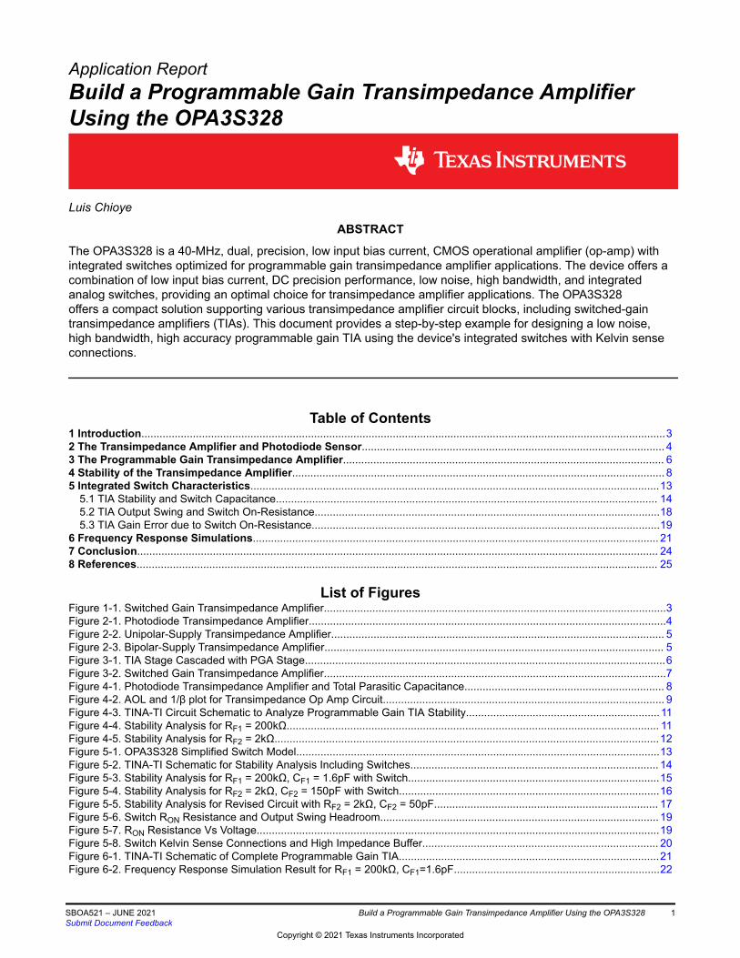
Application ReportBuild a Programmable Gain Transimpedance Amplifier Using the OPA3S328
Luis Chioye
ABSTRACT
The OPA3S328 is a 40-MHz, dual, precision, low input bias current, CMOS operational amplifier (op-amp) with integrated switches optimized for programmable gain transimpedance amplifier applications. The device offers a combination of low input bias current, DC precision performance, low noise, high bandwidth, and integrated analog switches, providing an optimal choice for transimpedance amplifier applications. The OPA3S328 offers a compact solution supporting various transimpedance amplifier circuit blocks, including switched-gain transimpedance amplifiers (TIAs). This document provides a step-by-step example for designing a low noise, high bandwidth, high accuracy programmable gain TIA using the device's integrated switches with Kelvin sense connections.
Table of Contents1 Introduction.............................................................................................................................................................................32 The Transimpedance Amplifier and Photodiode Sensor.................................................................................................... 43 The Programmable Gain Transimpedance Amplifier.......................................................................................................... 64 Stability of the Transimpedance Amplifier........................................................................................................................... 85 Integrated Switch Characteristics.......................................................................................................................................13
5.1 TIA Stability and Switch Capacitance.............................................................................................................................. 145.2 TIA Output Swing and Switch On-Resistance..................................................................................................................185.3 TIA Gain Error due to Switch On-Resistance...................................................................................................................19
6 Frequency Response Simulations...................................................................................................................................... 217 Conclusion............................................................................................................................................................................ 248 References............................................................................................................................................................................ 25
List of FiguresFigure 1-1. Switched Gain Transimpedance Amplifier.................................................................................................................3Figure 2-1. Photodiode Transimpedance Amplifier......................................................................................................................4Figure 2-2. Unipolar-Supply Transimpedance Amplifier.............................................................................................................. 5Figure 2-3. Bipolar-Supply Transimpedance Amplifier................................................................................................................ 5Figure 3-1. TIA Stage Cascaded with PGA Stage.......................................................................................................................6Figure 3-2. Switched Gain Transimpedance Amplifier.................................................................................................................7Figure 4-1. Photodiode Transimpedance Amplifier and Total Parasitic Capacitance.................................................................. 8Figure 4-2. AOL and 1/β plot for Transimpedance Op Amp Circuit............................................................................................. 9Figure 4-3. TINA-TI Circuit Schematic to Analyze Programmable Gain TIA Stability................................................................11Figure 4-4. Stability Analysis for RF1 = 200kΩ........................................................................................................................... 11Figure 4-5. Stability Analysis for RF2 = 2kΩ...............................................................................................................................12Figure 5-1. OPA3S328 Simplified Switch Model........................................................................................................................13Figure 5-2. TINA-TI Schematic for Stability Analysis Including Switches.................................................................................. 14Figure 5-3. Stability Analysis for RF1 = 200kΩ, CF1 = 1.6pF with Switch...................................................................................15Figure 5-4. Stability Analysis for RF2 = 2kΩ, CF2 = 150pF with Switch......................................................................................16Figure 5-5. Stability Analysis for Revised Circuit with RF2 = 2kΩ, CF2 = 50pF.......................................................................... 17Figure 5-6. Switch RON Resistance and Output Swing Headroom............................................................................................ 19Figure 5-7. RON Resistance Vs Voltage.....................................................................................................................................19Figure 5-8. Switch Kelvin Sense Connections and High Impedance Buffer.............................................................................. 20Figure 6-1. TINA-TI Schematic of Complete Programmable Gain TIA......................................................................................21Figure 6-2. Frequency Response Simulation Result for RF1 = 200kΩ, CF1=1.6pF....................................................................22
www.ti.com Table of Contents
SBOA521 – JUNE 2021Submit Document Feedback
Build a Programmable Gain Transimpedance Amplifier Using the OPA3S328 1
Copyright © 2021 Texas Instruments Incorporated
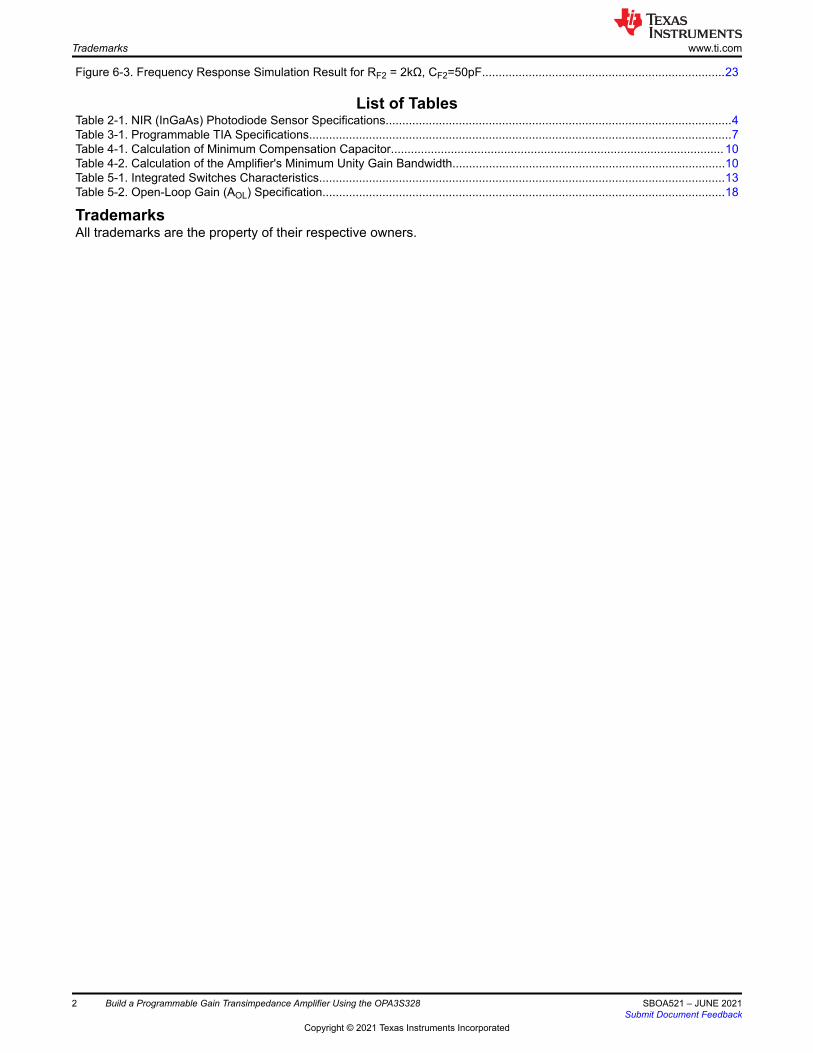
Figure 6-3. Frequency Response Simulation Result for RF2 = 2kΩ, CF2=50pF.........................................................................23
List of TablesTable 2-1. NIR (InGaAs) Photodiode Sensor Specifications........................................................................................................4Table 3-1. Programmable TIA Specifications...............................................................................................................................7Table 4-1. Calculation of Minimum Compensation Capacitor.................................................................................................... 10Table 4-2. Calculation of the Amplifier's Minimum Unity Gain Bandwidth..................................................................................10Table 5-1. Integrated Switches Characteristics..........................................................................................................................13Table 5-2. Open-Loop Gain (AOL) Specification.........................................................................................................................18
TrademarksAll trademarks are the property of their respective owners.
Trademarks www.ti.com
2 Build a Programmable Gain Transimpedance Amplifier Using the OPA3S328 SBOA521 – JUNE 2021Submit Document Feedback
Copyright © 2021 Texas Instruments Incorporated
1 IntroductionPhotodiode sensors produce a current output that changes with incident light, where the typical photocurrent changes orders of magnitude from hundreds of pico-amps to a few milliamps. Transimpedance amplifiers are essential circuits in photodiode acquisition systems to convert photocurrent to voltage that will drive a typical Analog-to-Digital (ADC) converter.
TIAs are required to amplify a photodiode's signal while meeting low-noise, high-resolution, and high-bandwidth constraints. A programmable gain TIA stage allows flexibility to measure the wide range of photodiode current while ensuring the amplifier remains inside its linear range. Programmable gain TIAs are essential in many systems. Applications include photosensor devices such as chemical analysis systems, infrared spectroscopes, data acquisition systems and optical communication applications where the optical power in a fiber can vary widely, and, as a result yield wide current ranges from an optical detector.
The OPA3S328 is a dual precision CMOS operational amplifier (op-amp) with integrated switches optimized for programmable gain transimpedance amplifier applications. The dual op-amp offers low input bias current, DC precision performance, low noise, high bandwidth, providing an optimal choice for transimpedance amplifier applications.
The simplified circuit diagram shown in Figure 1-1 shows a programmable gain TIA circuit implemented with the OPA3S328. The OPA3S328 integrates analog switches useful to select the TIA gains across multiple decades of photodiode current. The second-stage amplifier buffers the programmable gain TIA stage using Kelvin sense connections to eliminate errors due to the switch on-resistance, switch resistance drift, and non-linearity. This document provides a step-by-step example for designing a low noise, high bandwidth, high accuracy programmable TIA to perform optical power measurements using a near infrared (NIR) wavelength photodiode.
+
±
GND
RF1 200N
CF1
GND
VBIAS = -3 V
Photodiode
RF2 2 N
CF2
+
±
INSA OUTSA1
OUTSA2
OUTSB1
OUTSB2
OUTSB3
INSB
GAIN_2 N
GAIN_200 N
OPA3S328
U1A
OPA3S328
U1B
MUXOUT
VOUT
OPA3S328
Switch A OPA3S328
Switch B
Figure 1-1. Switched Gain Transimpedance Amplifier
www.ti.com Introduction
SBOA521 – JUNE 2021Submit Document Feedback
Build a Programmable Gain Transimpedance Amplifier Using the OPA3S328 3
Copyright © 2021 Texas Instruments Incorporated
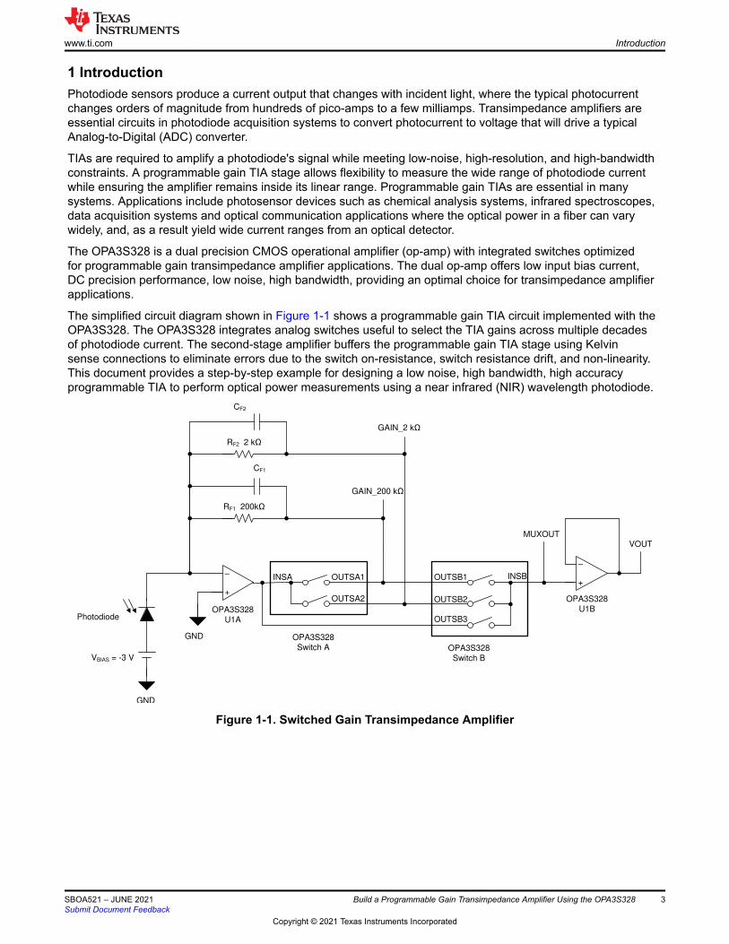
2 The Transimpedance Amplifier and Photodiode SensorA transimpedance amplifier consists of an op amp and a feedback resistor. The photosensor current to be amplified is applied to the inverting input, causing the output voltage of the amplifier to change, as shown in Figure 2-1:
+
±
RF
VBIAS = -3V
Photodiode
VOUT
CJ
Photodiode current (ID)
Photodiode parasitic junction
capacitance
-VEE
+VCC
VOUT= ID x RF
CF
Figure 2-1. Photodiode Transimpedance Amplifier
The feedback resistor (RF) across the op amp converts the photodiode current (ID) to a voltage (VOUT) using Ohm’s law, as shown in Equation 1.
OUT D F
V I R (1)
The feedback resistor (RF) determines the gain of the transimpedance op-amp. For the transimpedance current to voltage conversion to be accurate, the amplifier’s input bias current and input offset voltage must be small. The OPA3S328 offers low offset voltage, 25µV (max) and low input bias current, 0.2 pA. The photodiode parasitic junction capacitance plays a significant role in the stability and bandwidth of the TIA circuit, as we will discuss in detail in the following sections. The feedback capacitor (CF) is required to compensate the circuit for stability.
This example shows a large area near-infrared (NIR) wavelength Indium Gallium Arsenide (InGaAs) photodiode for the design. In this specific application, the photodiode operates on the photoconductive mode, where exposure to light causes a reverse current through the detector. A reverse bias is applied to the photosensor to reduce the junction capacitance. The reverse bias voltage (VR) dramatically improves the speed of response and linearity of the photodiode. The reverse bias increases the depletion region width and consequently decreases the junction capacitance. The dark current of this photosensor is about 50nA in this mode of operation. Table 2-1 shows the photodiode parameters.
Table 2-1. NIR (InGaAs) Photodiode Sensor SpecificationsParameter Symbol Value Unit
Reverse Voltage VR -3 V
Junction Capacitance (VR=-3V) CJ 100 pF
Reverse Current Range ID 0-2000 µA
Dark Current Idark 50 nA
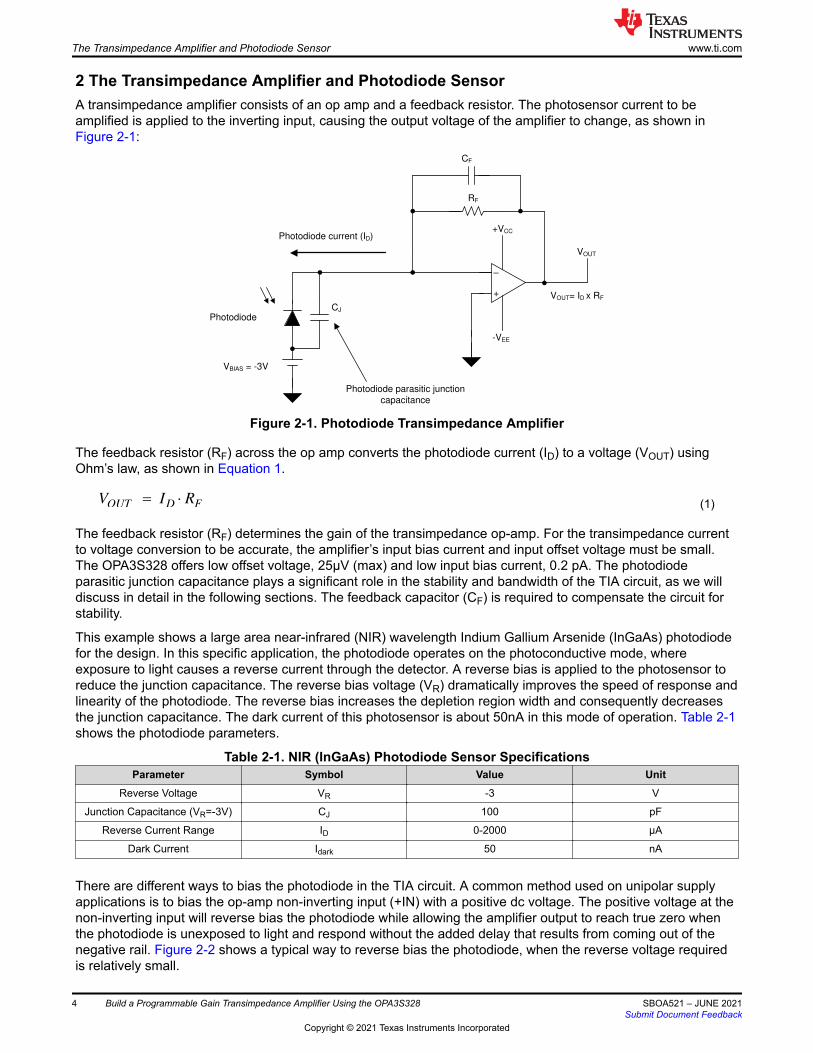
There are different ways to bias the photodiode in the TIA circuit. A common method used on unipolar supply applications is to bias the op-amp non-inverting input (+IN) with a positive dc voltage. The positive voltage at the non-inverting input will reverse bias the photodiode while allowing the amplifier output to reach true zero when the photodiode is unexposed to light and respond without the added delay that results from coming out of the negative rail. Figure 2-2 shows a typical way to reverse bias the photodiode, when the reverse voltage required is relatively small.
The Transimpedance Amplifier and Photodiode Sensor www.ti.com
4 Build a Programmable Gain Transimpedance Amplifier Using the OPA3S328 SBOA521 – JUNE 2021Submit Document Feedback
Copyright © 2021 Texas Instruments Incorporated
+
VBIAS
±
+VCC = +5 V
VOUT = VBIAS when ID = 0µA
ID
+
±
+
±
+
±
RF RF
VOUT
CJCJ
Photodiode current ( ID)
Photodiode parasitic junction
capacitance
CFCF
Figure 2-2. Unipolar-Supply Transimpedance Amplifier
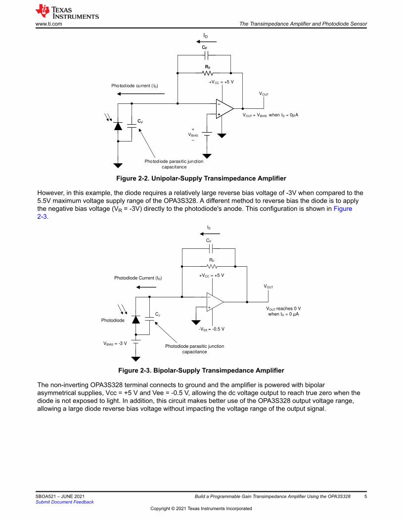
However, in this example, the diode requires a relatively large reverse bias voltage of -3V when compared to the 5.5V maximum voltage supply range of the OPA3S328. A different method to reverse bias the diode is to apply the negative bias voltage (VR = -3V) directly to the photodiode's anode. This configuration is shown in Figure 2-3.
+
±
RF
VBIAS = -3 V
Photodiode
VOUT
CJ
Photodiode Current (ID)
Photodiode parasitic junction capacitance
-VEE = -0.5 V
+VCC = +5 V
VOUT reaches 0 V when ID = 0 µA
CF
ID
Figure 2-3. Bipolar-Supply Transimpedance Amplifier
The non-inverting OPA3S328 terminal connects to ground and the amplifier is powered with bipolar asymmetrical supplies, Vcc = +5 V and Vee = -0.5 V, allowing the dc voltage output to reach true zero when the diode is not exposed to light. In addition, this circuit makes better use of the OPA3S328 output voltage range, allowing a large diode reverse bias voltage without impacting the voltage range of the output signal.
www.ti.com The Transimpedance Amplifier and Photodiode Sensor
SBOA521 – JUNE 2021Submit Document Feedback
Build a Programmable Gain Transimpedance Amplifier Using the OPA3S328 5
Copyright © 2021 Texas Instruments Incorporated
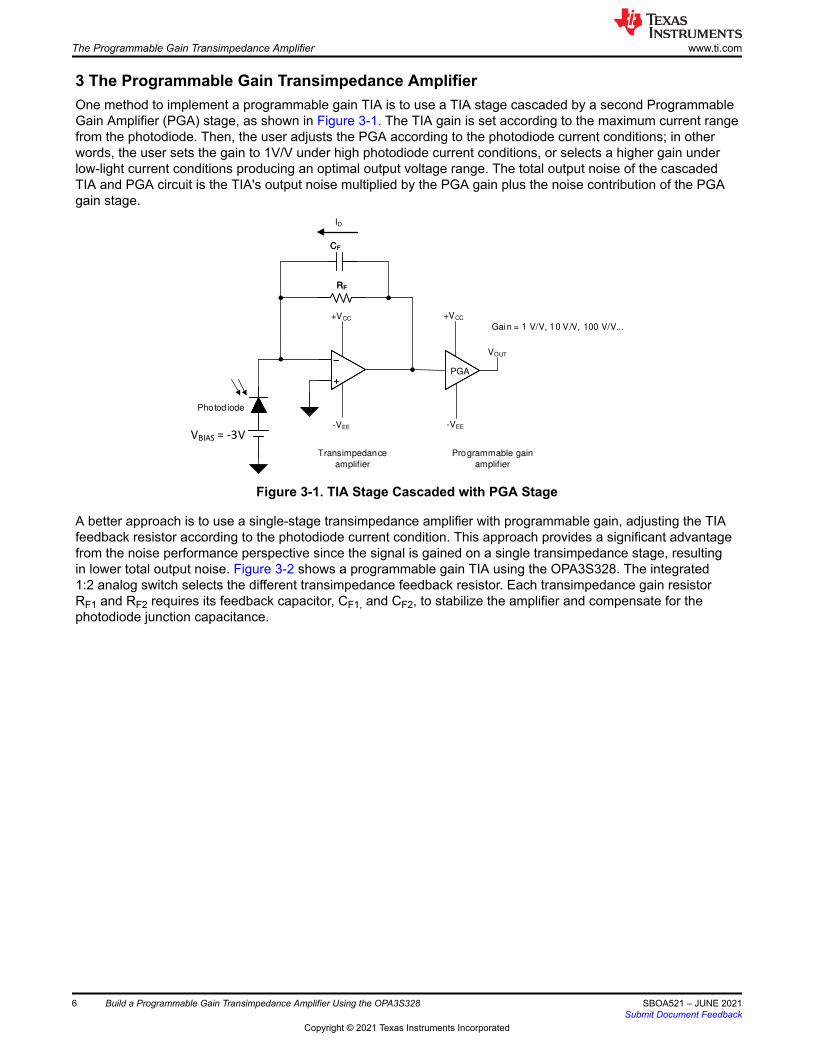
3 The Programmable Gain Transimpedance AmplifierOne method to implement a programmable gain TIA is to use a TIA stage cascaded by a second Programmable Gain Amplifier (PGA) stage, as shown in Figure 3-1. The TIA gain is set according to the maximum current range from the photodiode. Then, the user adjusts the PGA according to the photodiode current conditions; in other words, the user sets the gain to 1V/V under high photodiode current conditions, or selects a higher gain under low-light current conditions producing an optimal output voltage range. The total output noise of the cascaded TIA and PGA circuit is the TIA's output noise multiplied by the PGA gain plus the noise contribution of the PGA gain stage.
+
±
+
±
+
±
RF RF
Photodiode
VOUT
-VEE
+VCC
CFCF
ID
-VEE
+VCC
Transimpedance
amplifier
Programmable gain
amplifier
Gain = 1 V/V, 10 V/V, 100 V/V...
PGA
VBIAS = -3V
Figure 3-1. TIA Stage Cascaded with PGA Stage
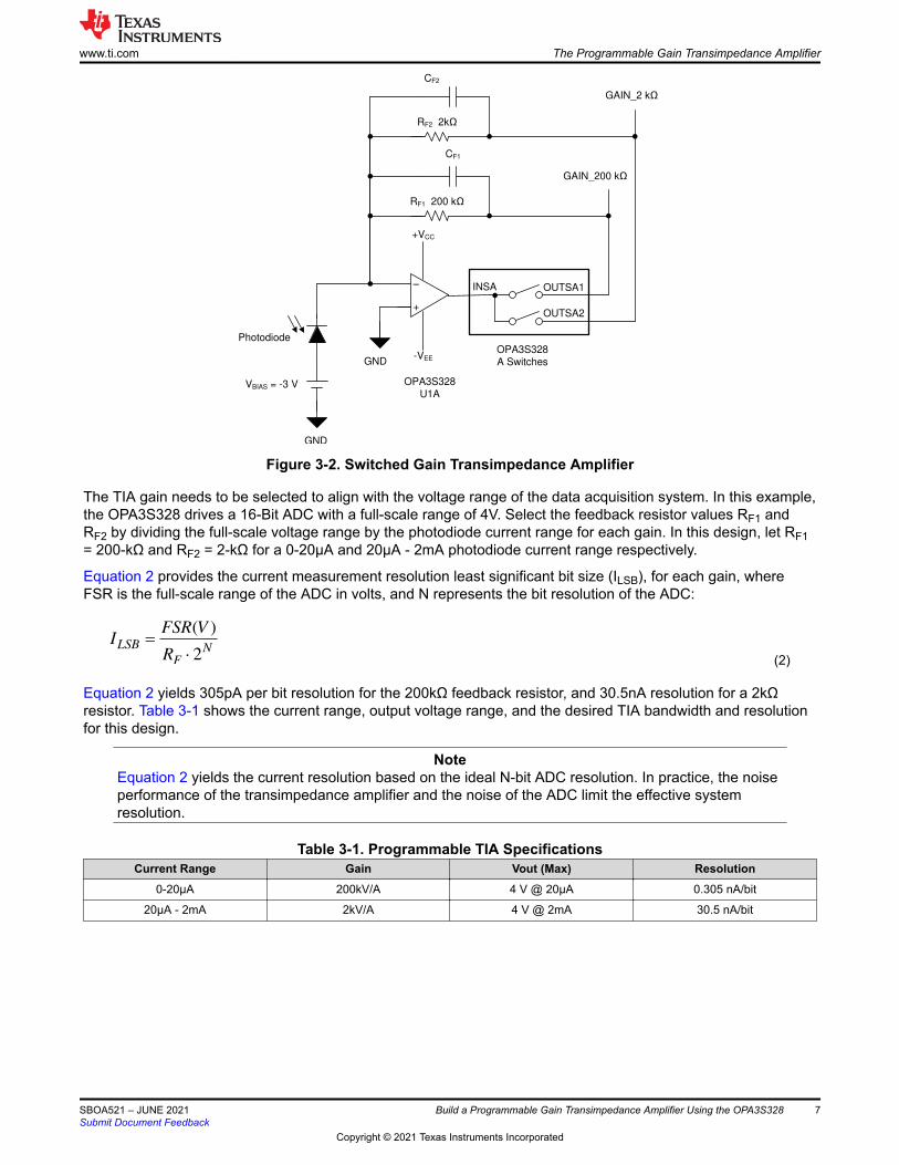
A better approach is to use a single-stage transimpedance amplifier with programmable gain, adjusting the TIA feedback resistor according to the photodiode current condition. This approach provides a significant advantage from the noise performance perspective since the signal is gained on a single transimpedance stage, resulting in lower total output noise. Figure 3-2 shows a programmable gain TIA using the OPA3S328. The integrated 1:2 analog switch selects the different transimpedance feedback resistor. Each transimpedance gain resistor RF1 and RF2 requires its feedback capacitor, CF1, and CF2, to stabilize the amplifier and compensate for the photodiode junction capacitance.
The Programmable Gain Transimpedance Amplifier www.ti.com
6 Build a Programmable Gain Transimpedance Amplifier Using the OPA3S328 SBOA521 – JUNE 2021Submit Document Feedback
Copyright © 2021 Texas Instruments Incorporated
+
±
GND
RF1 200 N
CF1
GND
VBIAS = -3 V
Photodiode
RF2 2N
CF2
INSA OUTSA1
OUTSA2
GAIN_2 N
GAIN_200 N
OPA3S328
U1A
OPA3S328
A Switches-VEE
+VCC
Figure 3-2. Switched Gain Transimpedance Amplifier
The TIA gain needs to be selected to align with the voltage range of the data acquisition system. In this example, the OPA3S328 drives a 16-Bit ADC with a full-scale range of 4V. Select the feedback resistor values RF1 and RF2 by dividing the full-scale voltage range by the photodiode current range for each gain. In this design, let RF1 = 200-kΩ and RF2 = 2-kΩ for a 0-20µA and 20µA - 2mA photodiode current range respectively.
Equation 2 provides the current measurement resolution least significant bit size (ILSB), for each gain, where FSR is the full-scale range of the ADC in volts, and N represents the bit resolution of the ADC:
( )
2LSB N
F
FSR VI
R
(2)
Equation 2 yields 305pA per bit resolution for the 200kΩ feedback resistor, and 30.5nA resolution for a 2kΩ resistor. Table 3-1 shows the current range, output voltage range, and the desired TIA bandwidth and resolution for this design.
NoteEquation 2 yields the current resolution based on the ideal N-bit ADC resolution. In practice, the noise performance of the transimpedance amplifier and the noise of the ADC limit the effective system resolution.
Table 3-1. Programmable TIA SpecificationsCurrent Range Gain Vout (Max) Resolution
0-20µA 200kV/A 4 V @ 20µA 0.305 nA/bit
20µA - 2mA 2kV/A 4 V @ 2mA 30.5 nA/bit
www.ti.com The Programmable Gain Transimpedance Amplifier
SBOA521 – JUNE 2021Submit Document Feedback
Build a Programmable Gain Transimpedance Amplifier Using the OPA3S328 7
Copyright © 2021 Texas Instruments Incorporated
4 Stability of the Transimpedance AmplifierThe circuit designer must verify the minimum necessary op-amp gain-bandwidth to guarantee stability and select the appropriate feedback compensation capacitor for each TIA gain. Therefore, it is essential to consider factors that affect TIA circuit stability carefully: the junction capacitance of the photodiode (CJ), the TIA gain, the desired closed-loop TIA bandwidth, and the unity gain-bandwidth product of the op-amp (fGBW).
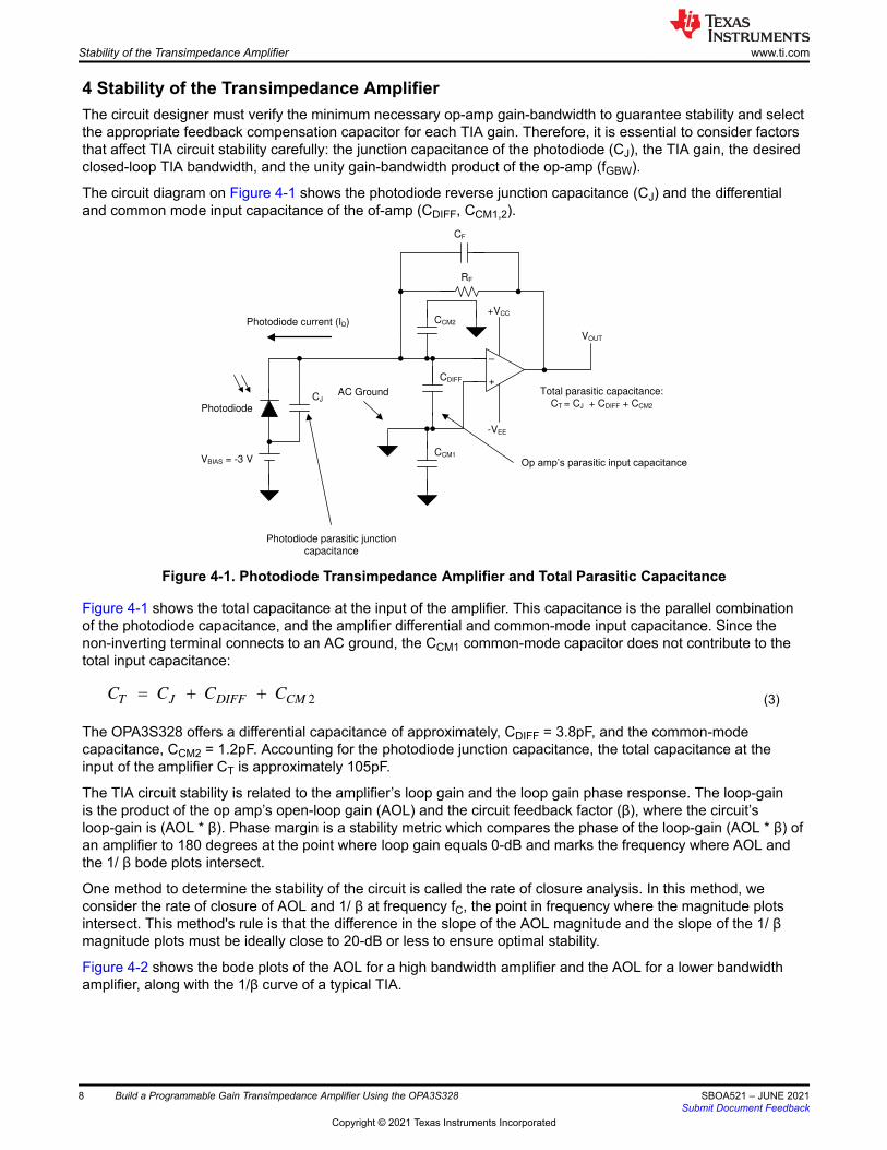
The circuit diagram on Figure 4-1 shows the photodiode reverse junction capacitance (CJ) and the differential and common mode input capacitance of the of-amp (CDIFF, CCM1,2).
+
±
RF
VBIAS = -3 V
Photodiode
VOUT
CJ
CDIFF
CCM2
CCM1
Photodiode current (ID)
Photodiode parasitic junction
capacitance
2SDPS¶VSDUDVLWLFLQSXWFDSDFLWDQFH
-VEE
+VCC
CF
Total parasitic capacitance:
CT = CJ + CDIFF + CCM2
AC Ground
Figure 4-1. Photodiode Transimpedance Amplifier and Total Parasitic Capacitance
Figure 4-1 shows the total capacitance at the input of the amplifier. This capacitance is the parallel combination of the photodiode capacitance, and the amplifier differential and common-mode input capacitance. Since the non-inverting terminal connects to an AC ground, the CCM1 common-mode capacitor does not contribute to the total input capacitance:
2
T J DIFF CMC C C C (3)
The OPA3S328 offers a differential capacitance of approximately, CDIFF = 3.8pF, and the common-mode capacitance, CCM2 = 1.2pF. Accounting for the photodiode junction capacitance, the total capacitance at the input of the amplifier CT is approximately 105pF.
The TIA circuit stability is related to the amplifier’s loop gain and the loop gain phase response. The loop-gain is the product of the op amp’s open-loop gain (AOL) and the circuit feedback factor (β), where the circuit’s loop-gain is (AOL * β). Phase margin is a stability metric which compares the phase of the loop-gain (AOL * β) of an amplifier to 180 degrees at the point where loop gain equals 0-dB and marks the frequency where AOL and the 1/ β bode plots intersect.
One method to determine the stability of the circuit is called the rate of closure analysis. In this method, we consider the rate of closure of AOL and 1/ β at frequency fC, the point in frequency where the magnitude plots intersect. This method's rule is that the difference in the slope of the AOL magnitude and the slope of the 1/ β magnitude plots must be ideally close to 20-dB or less to ensure optimal stability.
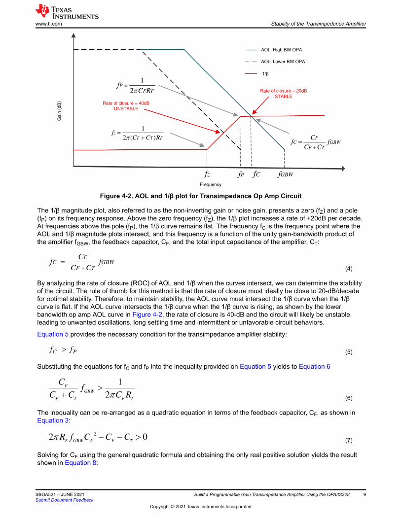
Figure 4-2 shows the bode plots of the AOL for a high bandwidth amplifier and the AOL for a lower bandwidth amplifier, along with the 1/β curve of a typical TIA.
Stability of the Transimpedance Amplifier www.ti.com
8 Build a Programmable Gain Transimpedance Amplifier Using the OPA3S328 SBOA521 – JUNE 2021Submit Document Feedback
Copyright © 2021 Texas Instruments Incorporated
1
2 ( )z
F T Ff
C C R
S
1
2P
F Ff
C R
S
FC GBW
F T
Cf f
C C
zf Pf Cf GBWf
Rate of closure = 20dB
STABLE
Rate of closure = 40dB
UNSTABLE
Frequency
Ga
in (
dB
)
AOL: High BW OPA
AOL: Lower BW OPA
1/
Figure 4-2. AOL and 1/β plot for Transimpedance Op Amp Circuit
The 1/β magnitude plot, also referred to as the non-inverting gain or noise gain, presents a zero (fZ) and a pole (fP) on its frequency response. Above the zero frequency (fZ), the 1/β plot increases a rate of +20dB per decade. At frequencies above the pole (fP), the 1/β curve remains flat. The frequency fC is the frequency point where the AOL and 1/β magnitude plots intersect, and this frequency is a function of the unity gain-bandwidth product of the amplifier fGBW, the feedback capacitor, CF, and the total input capacitance of the amplifier, CT:
F
C GBWF T
Cf f
C C
(4)
By analyzing the rate of closure (ROC) of AOL and 1/β when the curves intersect, we can determine the stability of the circuit. The rule of thumb for this method is that the rate of closure must ideally be close to 20-dB/decade for optimal stability. Therefore, to maintain stability, the AOL curve must intersect the 1/β curve when the 1/β curve is flat. If the AOL curve intersects the 1/β curve when the 1/β curve is rising, as shown by the lower bandwidth op amp AOL curve in Figure 4-2, the rate of closure is 40-dB and the circuit will likely be unstable, leading to unwanted oscillations, long settling time and intermittent or unfavorable circuit behaviors.
Equation 5 provides the necessary condition for the transimpedance amplifier stability:
C Pf f! (5)
Substituting the equations for fC and fP into the inequality provided on Equation 5 yields to Equation 6
1
2
F
GBW
F T F F
Cf
C C C R!
S (6)
The inequality can be re-arranged as a quadratic equation in terms of the feedback capacitor, CF, as shown in Equation 3:
2
2 0F GBW F F T
R f C C C !S (7)
Solving for CF using the general quadratic formula and obtaining the only real positive solution yields the result shown in Equation 8:
www.ti.com Stability of the Transimpedance Amplifier
SBOA521 – JUNE 2021Submit Document Feedback
Build a Programmable Gain Transimpedance Amplifier Using the OPA3S328 9
Copyright © 2021 Texas Instruments Incorporated
1
* 1 1 84
F F GBW T
F GBW
C R f CR f
! SS (8)
Equation 8 determines the minimum compensation capacitor to guarantee stability for the TIA design. Table 4-1 shows the minimum calculated compensation capacitors CF1 and CF2 to ensure stability for each TIA gain for the unity gain-bandwidth of the OPA3S328. The dominant pole frequency fP is a function of the feedback resistor and feedback capacitor for each TIA gain.
Table 4-1. Calculation of Minimum Compensation CapacitorfGBWAmplifier Unity Gain Bandwidth
TIA Gain CTTIA Total Input Capacitance
RFTIA Feedback Resistor
CFMin Feedback Capacitor for stability
fP Dominant Pole frequency
40 MHz 200 kV/A 105 pF 200 kΩ >1.5pF 530kHz
40 MHz 2 kV/A 105 pF 2 kΩ >16pF 4.97MHz
A different approach to ensure stability while meeting a TIA gain and bandwidth requirement, is to use the inequality provided in Equation 6, and solve for the amplifier's minimum unity gain-bandwidth (fGBW). Equation 9 provides the amplifier's minimum fGBW as a function of the feedback resistor RF, the feedback capacitor CF, and the total input capacitance of the amplifier CT:
2
2
F T
GBW
F F
C Cf
C R
!
S (9)
Equation 9 determines the amplifier's minimum required unity gain-bandwidth to guarantee stability for a TIA design. Therefore, higher bandwidth amplifiers support higher gain and bandwidth TIA circuits, and tolerate higher photodiode capacitance while remaining stable.
On this programmable gain TIA example, the desired closed-loop bandwidth TIABW is 500kHz. Therefore, Equation 10 provides the maximum compensation capacitance CF while meeting the closed loop TIA bandwidth requirement:
1 <
2F
F BW
CR TIAS (10)
Equation 10 shows the calculated compensation capacitors CF1 and CF2 for each gain to meet the TIA closed-loop bandwidth requirement and the required amplifier's minimum unity gain-bandwidth to ensure stability:
Table 4-2. Calculation of the Amplifier's Minimum Unity Gain BandwidthTIA Gain TIABW
Desired TIA Bandwidth
CTTIA Total Input Capacitance
RFTIA Feedback Resistor
CFFeedback Capacitor for TIABW
fGBWMin Amplifier Unity Gain BW
200 kV/A 500 kHz 105 pF 200 kΩ 1.6pF > 33.8MHz
2 kV/A 500 kHz 105 pF 2 kΩ 159pF > 834 kHz
The OPA3S328 offers a unity gain bandwidth of 40 MHz, and therefore, can support the desired TIA gain and bandwidth requirements for the design. Select standard values for the compensation capacitor, CF1 = 1.6pF for TIA gain of 200kV/A and CF2 of 150pF for TIA gain of 2kV/A.
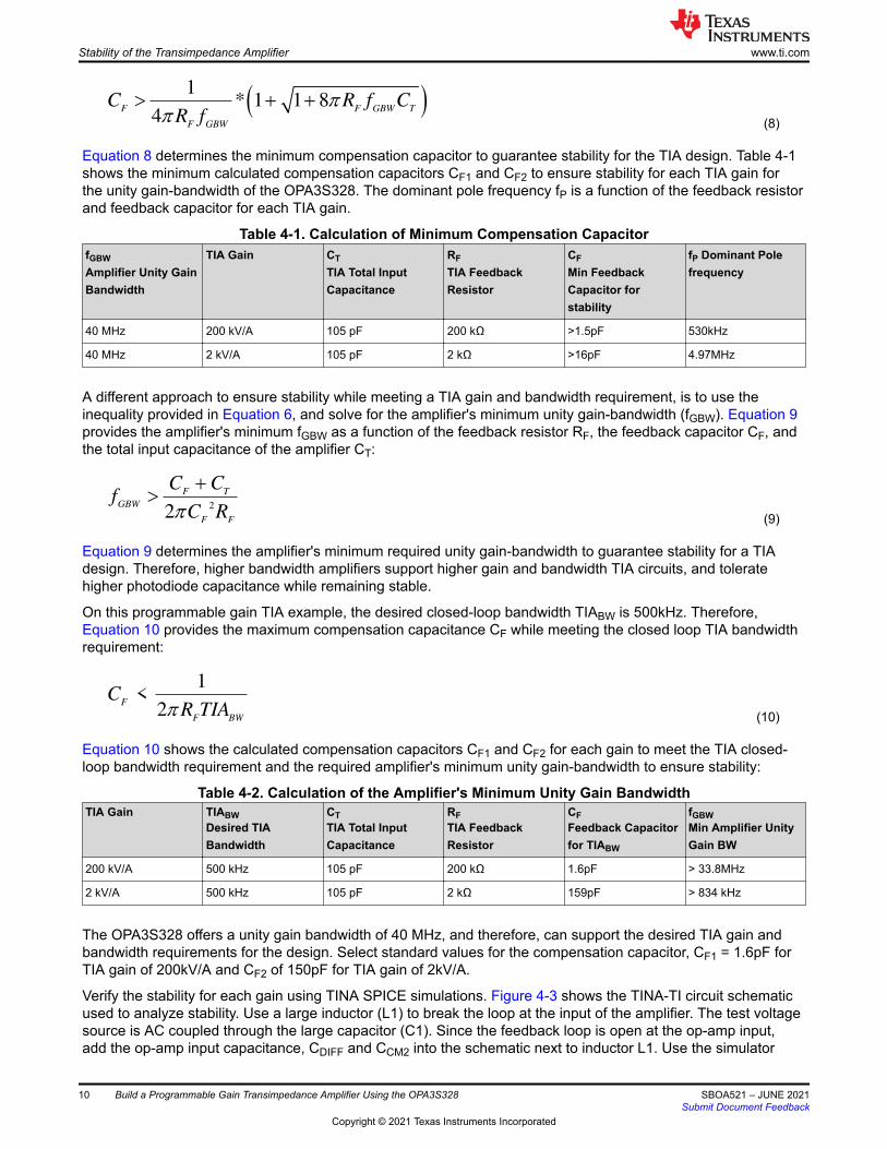
Verify the stability for each gain using TINA SPICE simulations. Figure 4-3 shows the TINA-TI circuit schematic used to analyze stability. Use a large inductor (L1) to break the loop at the input of the amplifier. The test voltage source is AC coupled through the large capacitor (C1). Since the feedback loop is open at the op-amp input, add the op-amp input capacitance, CDIFF and CCM2 into the schematic next to inductor L1. Use the simulator
Stability of the Transimpedance Amplifier www.ti.com
10 Build a Programmable Gain Transimpedance Amplifier Using the OPA3S328 SBOA521 – JUNE 2021Submit Document Feedback
Copyright © 2021 Texas Instruments Incorporated
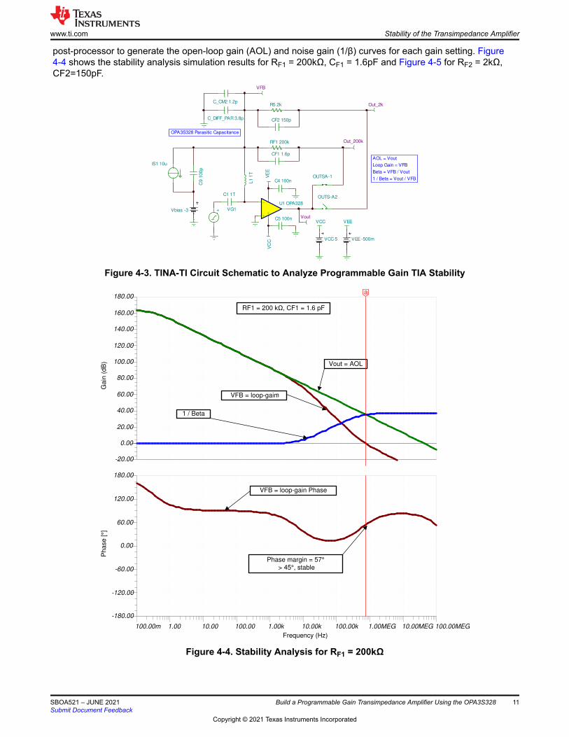
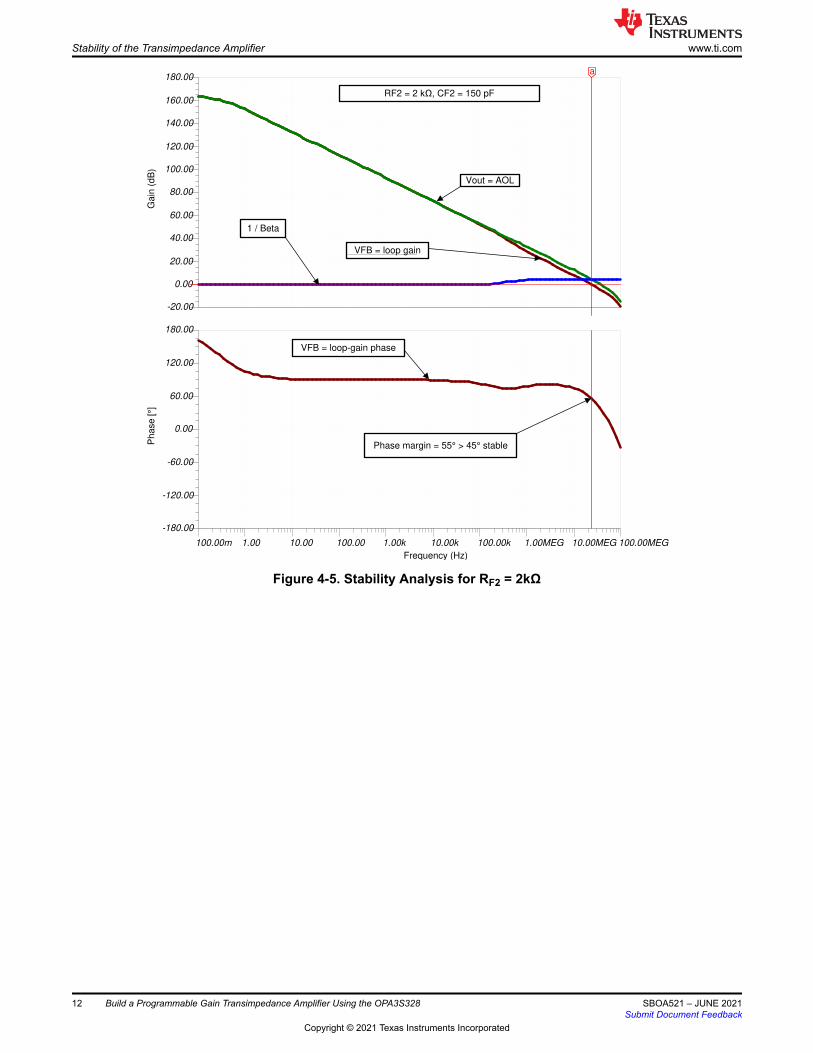
post-processor to generate the open-loop gain (AOL) and noise gain (1/β) curves for each gain setting. Figure 4-4 shows the stability analysis simulation results for RF1 = 200kΩ, CF1 = 1.6pF and Figure 4-5 for RF2 = 2kΩ, CF2=150pF.
VCC VEE
VC
CV
EE
C5 100n
C4 100n
-
++
U1 OPA328
OUTS-A2
OUTSA-1
R5 2k
RF1 200k
C9 1
00p
IS1 10u
Out_200k
Out_2k
CF1 1.6p
VCC 5 VEE -500m
L1 1
T
C_DIFF_PAR 3.8p
C_CM2 1.2p
C1 1T
+ VG1
CF2 150p
VFB
Vbias -3
Vout
AOL = Vout
Loop Gain = VFB
Beta = VFB / Vout
1 / Beta = Vout / VFB
OPA3S328 Parasitic Capacitance
Figure 4-3. TINA-TI Circuit Schematic to Analyze Programmable Gain TIA Stability
T
VFB = Loop-Gain
Vout = AOL
1 / Beta
Ga
in (
dB
)
-20.00
0.00
20.00
40.00
60.00
80.00
100.00
120.00
140.00
160.00
180.00
Frequency (Hz)
100.00m 1.00 10.00 100.00 1.00k 10.00k 100.00k 1.00MEG 10.00MEG 100.00MEG
Ph
ase
[°]
-180.00
-120.00
-60.00
0.00
60.00
120.00
180.00
1 / Beta
VFB = loop-gain
VFB = loop-gain Phase
Phase margin = 57°
> 45°, stable
RF1 = 200 N, CF1 = 1.6 pF
a
Figure 4-4. Stability Analysis for RF1 = 200kΩ
www.ti.com Stability of the Transimpedance Amplifier
SBOA521 – JUNE 2021Submit Document Feedback
Build a Programmable Gain Transimpedance Amplifier Using the OPA3S328 11
Copyright © 2021 Texas Instruments Incorporated
T
VFB = Loop Gain
Vout = AOL
1 / Beta
VFB = Loop-Gain Phase
Phase Margin = 55 degrees
>45-degrees Stable
Ga
in (
dB
)
-20.00
0.00
20.00
40.00
60.00
80.00
100.00
120.00
140.00
160.00
180.00
Frequency (Hz)
100.00m 1.00 10.00 100.00 1.00k 10.00k 100.00k 1.00MEG 10.00MEG 100.00MEG
Ph
ase
[°]
-180.00
-120.00
-60.00
0.00
60.00
120.00
180.00
Phase margin = 55° > 45° stable
RF2 = 2 N, CF2 = 150 pF
VFB = loop-gain phase
1 / Beta
VFB = loop gain
Vout = AOL
a
Figure 4-5. Stability Analysis for RF2 = 2kΩ
Stability of the Transimpedance Amplifier www.ti.com
12 Build a Programmable Gain Transimpedance Amplifier Using the OPA3S328 SBOA521 – JUNE 2021Submit Document Feedback
Copyright © 2021 Texas Instruments Incorporated
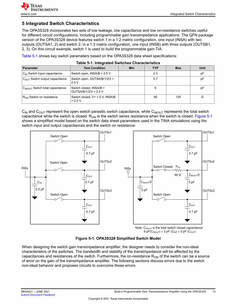
5 Integrated Switch CharacteristicsThe OPA3S328 incorporates two sets of low leakage, low capacitance and low on-resistance switches useful for different circuit configurations, including programmable gain transimpedance applications. The QFN package version of the OPA3S328 device features switch 1 in a 1:2 matrix configuration, one input (INSA) with two outputs (OUTSA1, 2) and switch 2, in a 1:3 matrix configuration, one input (INSB) with three outputs (OUTSB1, 2, 3). On this circuit example, switch 1 is used to build the programmable gain TIA.
Table 5-1 shows key switch parameters based on the OPA3S328 data sheet specifications:
Table 5-1. Integrated Switches CharacteristicsParameter Test Condition Min TYP Max UnitCIN Switch input capacitance Switch open, INSA/B = 2.5 V 2.3 pF
COUT Switch output capacitance Switch open, OUTSA/B/1/2/3 = 2.5 V
0.7 pF
CINOUT Switch total capacitance Switch closed, INSA/B = OUTSA/B/1/2/3 = 2.5 V
6 pF
RON Switch on resistance Switch closed, V+ = 5 V, INSA/B = 2.5 V
90 125 Ω
CIN and COUT represent the open switch parasitic switch capacitance, while CINOUT represents the total switch capacitance while the switch is closed. RON is the switch series resistance when the switch is closed. Figure 5-1 shows a simplified model based on the switch data sheet parameters used in the TINA simulations using the switch input and output capacitances and the switch on resistance:
COUT
0.7 pF
Switch Open
OUTSx1
0.7 pF
COUT
0.7 pF
Switch Open
OUTSx2
OUTSx3
INSx
COUT
0.7 pF
Switch Open
OUTSx1
RON
3 pF
3 pF
Switch Closed
COUT
0.7 pF
Switch Open
OUTSx2
OUTSx3
INSx
90
Note: CINOUT is the total switch closed capacitance:
6 pF(CINOUT) = 3 pF (CIN) + 3 pF (COUT)
CINOUT/2
CINOUT/2
Switch Open
COUT
CIN
2.3 pF
Figure 5-1. OPA3S328 Simplified Switch Model
When designing the switch gain transimpedance amplifier, the designer needs to consider the non-ideal characteristics of the switches. The bandwidth and stability of the transimpedance will be affected by the capacitances and resistances of the switch. Furthermore, the on-resistance RON of the switch can be a source of error on the gain of the transimpedance amplifier. The following sections discuss errors due to the switch non-ideal behavior and proposes circuits to overcome these errors.
www.ti.com Integrated Switch Characteristics
SBOA521 – JUNE 2021Submit Document Feedback
Build a Programmable Gain Transimpedance Amplifier Using the OPA3S328 13
Copyright © 2021 Texas Instruments Incorporated
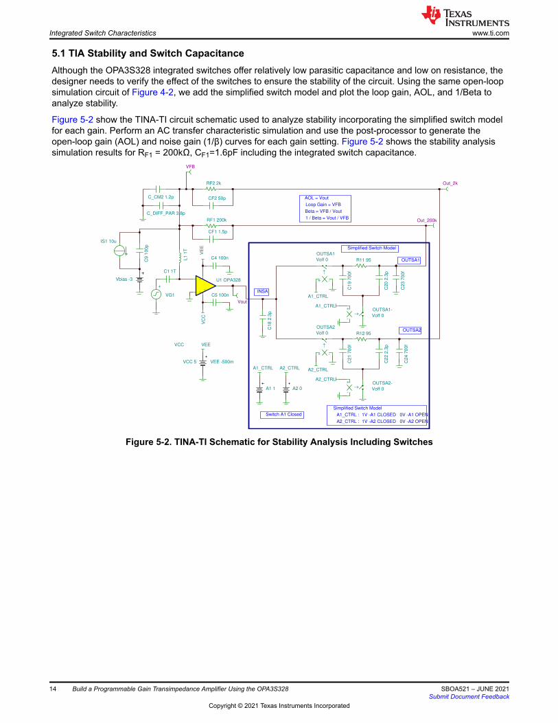
5.1 TIA Stability and Switch CapacitanceAlthough the OPA3S328 integrated switches offer relatively low parasitic capacitance and low on resistance, the designer needs to verify the effect of the switches to ensure the stability of the circuit. Using the same open-loop simulation circuit of Figure 4-2, we add the simplified switch model and plot the loop gain, AOL, and 1/Beta to analyze stability.
Figure 5-2 show the TINA-TI circuit schematic used to analyze stability incorporating the simplified switch model for each gain. Perform an AC transfer characteristic simulation and use the post-processor to generate the open-loop gain (AOL) and noise gain (1/β) curves for each gain setting. Figure 5-2 shows the stability analysis simulation results for RF1 = 200kΩ, CF1=1.6pF including the integrated switch capacitance.
VCC VEE
VC
CV
EE
A1_CTRL
A1_CTRL
A2_CTRL
A2_CTRL
A1_CTRL A2_CTRL
C5 100n
C4 100n
-
++
U1 OPA328
RF2 2k
RF1 200k
C9
10
0p
IS1 10u
Out_200k
Out_2k
CF1 1.5p
VCC 5 VEE -500m
L1
1T
C1 1T
+
VG1
CF2 50p
VFB
C_CM2 1.2p
C_DIFF_PAR 3.8p
Vbias -3
C1
8 2
.3p
-+o
OUTSA1
Voff 0 R11 95
C1
9 7
00f
-
+o
OUTSA1-
Voff 0
C2
0 2
.3p
-+o
OUTSA2
Voff 0 R12 95
C2
1 7
00f
-
+o
OUTSA2-
Voff 0C
22
2.3
p
C2
3 7
00f
C2
4 7
00f
A1 1 A2 0
Vout
AOL = Vout
Loop Gain = VFB
Beta = VFB / Vout
1 / Beta = Vout / VFB
INSA
OUTSA1
Simplified Switch Model
OUTSA2
Simplified Switch Model
A1_CTRL : 1V -A1 CLOSED 0V -A1 OPEN
A2_CTRL : 1V -A2 CLOSED 0V -A2 OPEN
Switch A1 Closed
Figure 5-2. TINA-TI Schematic for Stability Analysis Including Switches
Integrated Switch Characteristics www.ti.com
14 Build a Programmable Gain Transimpedance Amplifier Using the OPA3S328 SBOA521 – JUNE 2021Submit Document Feedback
Copyright © 2021 Texas Instruments Incorporated
T
Loop-Gain = VFB
Vout = AOL
1 / Beta
Rate of Closure = ~ -20dB / Decade
Phase Margin = 54.6 degrees
VFB = Loop-Gain Phase
Ga
in (
dB
)
-20.00
0.00
20.00
40.00
60.00
80.00
100.00
Frequency (Hz)
1.00k 10.00k 100.00k 1.00MEG 10.00MEG 100.00MEG
Ph
ase
[°]
-180.00
-120.00
-60.00
0.00
60.00
120.00
180.00
RF1 = 200 N, CF1 =1.6 pF
(with switches)
VFB = loop-gain phase
Phase margin = 54.6° > 45° stable
Rate of closure = ~ -20 dB / decade
1 / Beta
Loop-Gain = VFB
Vout = AOL
a
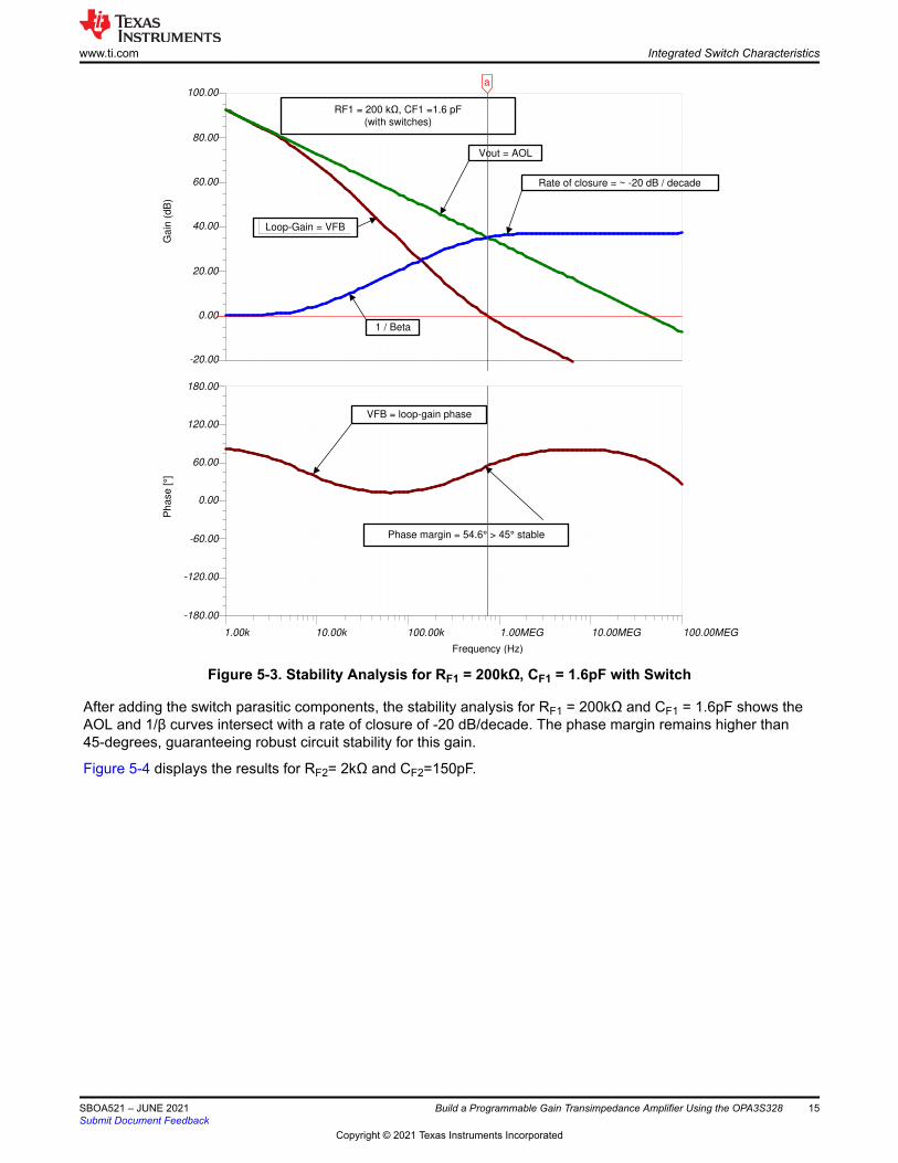
Figure 5-3. Stability Analysis for RF1 = 200kΩ, CF1 = 1.6pF with Switch
After adding the switch parasitic components, the stability analysis for RF1 = 200kΩ and CF1 = 1.6pF shows the AOL and 1/β curves intersect with a rate of closure of -20 dB/decade. The phase margin remains higher than 45-degrees, guaranteeing robust circuit stability for this gain.
Figure 5-4 displays the results for RF2= 2kΩ and CF2=150pF.
www.ti.com Integrated Switch Characteristics
SBOA521 – JUNE 2021Submit Document Feedback
Build a Programmable Gain Transimpedance Amplifier Using the OPA3S328 15
Copyright © 2021 Texas Instruments Incorporated
T
Ga
in (
dB
)
-20.00
0.00
20.00
40.00
60.00
80.00
100.00
Frequency (Hz)
1.00k 10.00k 100.00k 1.00MEG 10.00MEG 100.00MEG 1.00G
Ph
ase
[°]
-180.00
-120.00
-60.00
0.00
60.00
120.00
180.00
RF2=2 k, CF2 = 150 pF
a
Phase Margin = 35.8°
VFB = loop-gain phase
1 / Beta
Loop-gain = VFB
fz2 = ~27 MHz
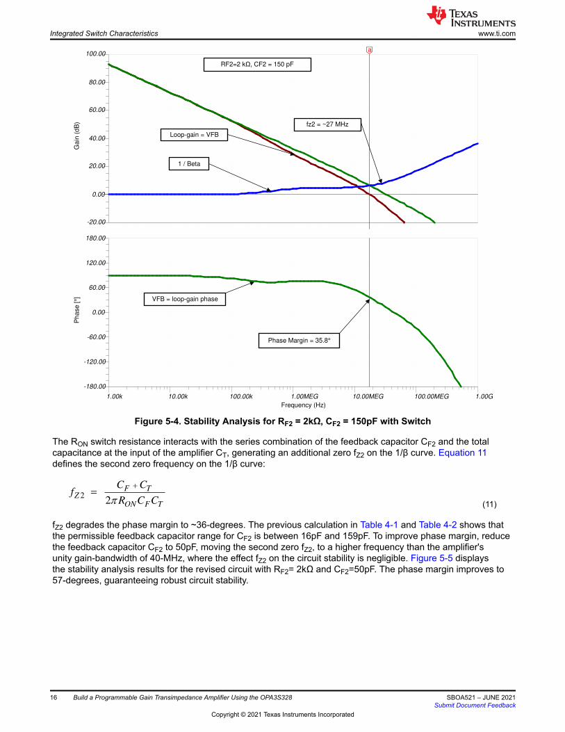
Figure 5-4. Stability Analysis for RF2 = 2kΩ, CF2 = 150pF with Switch
The RON switch resistance interacts with the series combination of the feedback capacitor CF2 and the total capacitance at the input of the amplifier CT, generating an additional zero fZ2 on the 1/β curve. Equation 11 defines the second zero frequency on the 1/β curve:
2
2
F TZ
ON F T
C Cf
R C C
S (11)
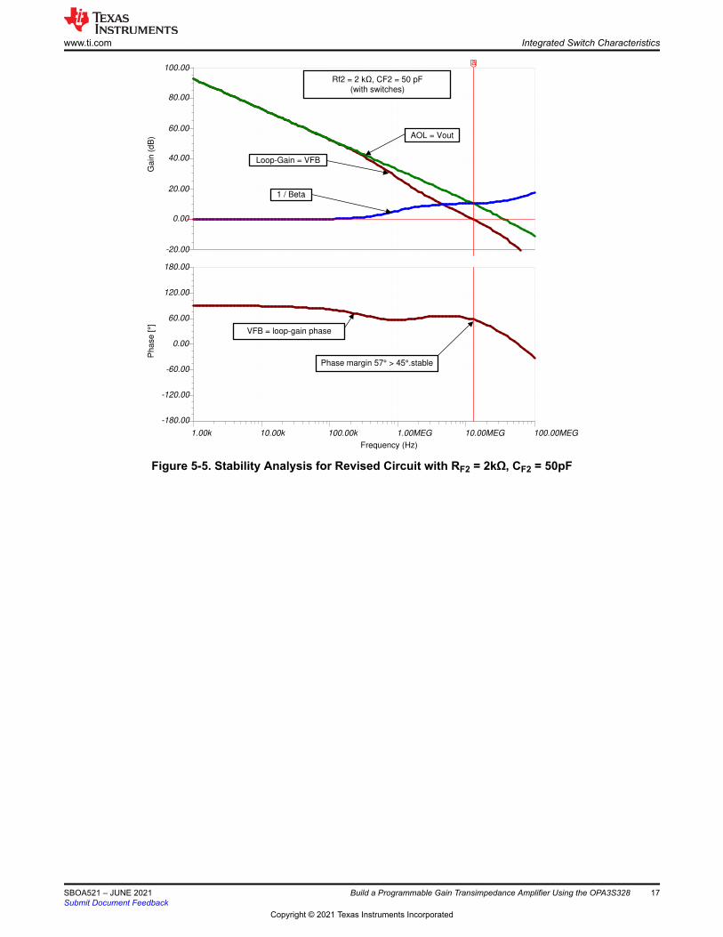
fZ2 degrades the phase margin to ~36-degrees. The previous calculation in Table 4-1 and Table 4-2 shows that the permissible feedback capacitor range for CF2 is between 16pF and 159pF. To improve phase margin, reduce the feedback capacitor CF2 to 50pF, moving the second zero fZ2, to a higher frequency than the amplifier's unity gain-bandwidth of 40-MHz, where the effect fZ2 on the circuit stability is negligible. Figure 5-5 displays the stability analysis results for the revised circuit with RF2= 2kΩ and CF2=50pF. The phase margin improves to 57-degrees, guaranteeing robust circuit stability.
Integrated Switch Characteristics www.ti.com
16 Build a Programmable Gain Transimpedance Amplifier Using the OPA3S328 SBOA521 – JUNE 2021Submit Document Feedback
Copyright © 2021 Texas Instruments Incorporated
T
AOL=Vout
1 / Beta
Ga
in (
dB
)
-20.00
0.00
20.00
40.00
60.00
80.00
100.00
Frequency (Hz)
1.00k 10.00k 100.00k 1.00MEG 10.00MEG 100.00MEG
Ph
ase
[°]
-180.00
-120.00
-60.00
0.00
60.00
120.00
180.00
1 / Beta
Loop-Gain = VFB
AOL = Vout
Rf2 = 2 N, CF2 = 50 pF
(with switches)
a
Phase margin 57° > 45°.stable
VFB = loop-gain phase
Figure 5-5. Stability Analysis for Revised Circuit with RF2 = 2kΩ, CF2 = 50pF
www.ti.com Integrated Switch Characteristics
SBOA521 – JUNE 2021Submit Document Feedback
Build a Programmable Gain Transimpedance Amplifier Using the OPA3S328 17
Copyright © 2021 Texas Instruments Incorporated
5.2 TIA Output Swing and Switch On-ResistanceWhen building a programmable gain TIA with analog switches, the circuit designer needs to account for the voltage drop across the switch RON resistance when the photodiode current flows through the amplifier's feedback. This voltage drop is significant at the higher photodiode current ranges.
Amplifier output stages that can swing close to the complete span between negative and positive supply voltage are generally known as rail-to-rail output (RRO) stages. Most RRO stages can swing within tens of millivolts of the rails. The amplifier's data sheet specifies the output voltage range from the supplies as output swing (output voltage low/high). Although the OPA3s328 offers an RRO stage and the amplifier functions in this region, the performance gradually degrades as the output gets closer to the rails where the amplifier open-loop gain decreases. Therefore, it is advisable to allow extra headroom in applications that require very low distortion. A conservative approach to ensure the amplifier remains well within its linear region is to use the output swing headroom from supply from the data sheet open-loop gain (AOL) specification:
Table 5-2. Open-Loop Gain (AOL) SpecificationParameter Test Condition Min TYP Max UnitAOLOpen-loop voltage gain
(V–) + 200 mV < VO < (V+) – 200 mVRL = 2 kΩ
108 123 dB
The OPA3S328 data sheet output swing specification during the AOL test is 200mV from the rail with a 2kΩ load referred to mid-supply, while the device is powered with a 5.5V supply. This AOL test condition corresponds to an equivalent load current of approximately 1.275mA. In this TIA example, the OPA3S328 sources a maximum of 2mA of current, therefore, the designer must allow headroom exceeding >200mV.
The designer must carefully choose the maximum feedback resistor to meet the minimum headroom requirement. Equation 12 provides the maximum TIA feedback resistor value (RF) as a function of the supply voltage (VCC), the maximum diode current (ID_Max), the maximum on-resistance (RON_Max) while allowing the necessary output swing supply headroom (VHeadroom).
_
_
CC Headroom
F ON Max
D Max
V VR R
I
(12)
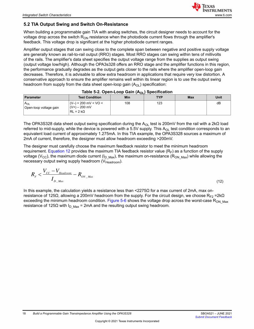
In this example, the calculation yields a resistance less than <2275Ω for a max current of 2mA, max on-resistance of 125Ω, allowing a 200mV headroom from the supply. For the circuit design, we choose RF2 =2kΩ exceeding the minimum headroom condition. Figure 5-6 shows the voltage drop across the worst-case RON_Max resistance of 125Ω with ID_Max = 2mA and the resulting output swing headroom.
Integrated Switch Characteristics www.ti.com
18 Build a Programmable Gain Transimpedance Amplifier Using the OPA3S328 SBOA521 – JUNE 2021Submit Document Feedback
Copyright © 2021 Texas Instruments Incorporated
+
±
GND
RF1 200 N
GND
VBIAS = -3 V
RF2 2 N
INSA
OUTSA1
OUTSA2
GAIN_2 N
GAIN_200 N
OPA3S328
U1A
OPA3S328
Switch A
RON_MAX 125
ID = 2 mA
ID = 2 mA
TIAOUTPUT = 4.000 V
VOUT1
4.250 V
ID = 2 mA
ID = 2 mA
+ 0.250 V -
ID = 2 mA
ID = 2 mA
VHEADROOM = +5 V ± 4.25 V
= 750 mV
Figure 5-6. Switch RON Resistance and Output Swing Headroom
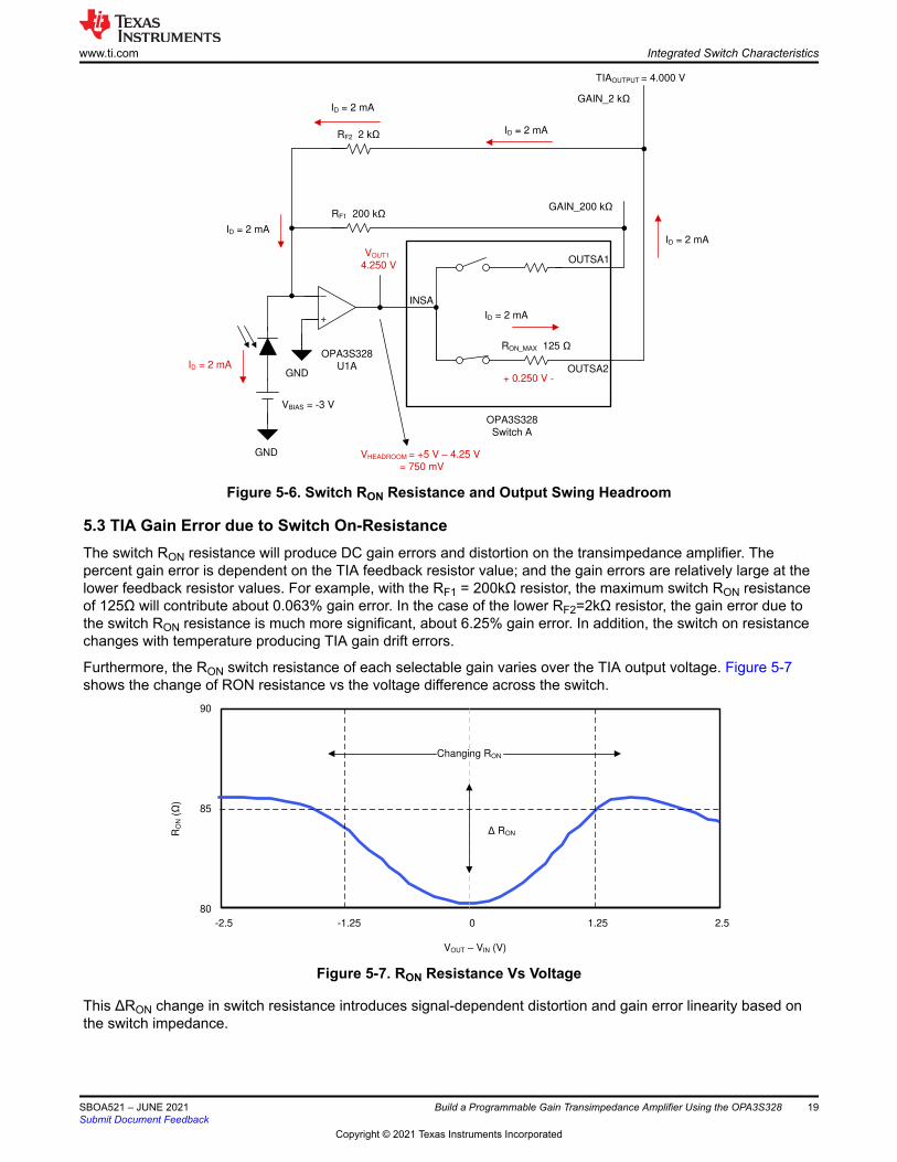
5.3 TIA Gain Error due to Switch On-ResistanceThe switch RON resistance will produce DC gain errors and distortion on the transimpedance amplifier. The percent gain error is dependent on the TIA feedback resistor value; and the gain errors are relatively large at the lower feedback resistor values. For example, with the RF1 = 200kΩ resistor, the maximum switch RON resistance of 125Ω will contribute about 0.063% gain error. In the case of the lower RF2=2kΩ resistor, the gain error due to the switch RON resistance is much more significant, about 6.25% gain error. In addition, the switch on resistance changes with temperature producing TIA gain drift errors.
Furthermore, the RON switch resistance of each selectable gain varies over the TIA output voltage. Figure 5-7 shows the change of RON resistance vs the voltage difference across the switch.
80
85
90
-2.5 -1.25 0 1.25 2.5
VOUT ± VIN (V)
RO
N (
)
ûRON
Changing RON
Figure 5-7. RON Resistance Vs Voltage
This ΔRON change in switch resistance introduces signal-dependent distortion and gain error linearity based on the switch impedance.
www.ti.com Integrated Switch Characteristics
SBOA521 – JUNE 2021Submit Document Feedback
Build a Programmable Gain Transimpedance Amplifier Using the OPA3S328 19
Copyright © 2021 Texas Instruments Incorporated
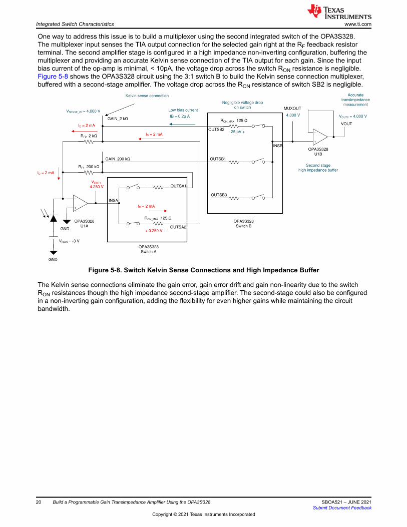
One way to address this issue is to build a multiplexer using the second integrated switch of the OPA3S328. The multiplexer input senses the TIA output connection for the selected gain right at the RF feedback resistor terminal. The second amplifier stage is configured in a high impedance non-inverting configuration, buffering the multiplexer and providing an accurate Kelvin sense connection of the TIA output for each gain. Since the input bias current of the op-amp is minimal, < 10pA, the voltage drop across the switch RON resistance is negligible. Figure 5-8 shows the OPA3S328 circuit using the 3:1 switch B to build the Kelvin sense connection multiplexer, buffered with a second-stage amplifier. The voltage drop across the RON resistance of switch SB2 is negligible.
+
±
GND
RF1 200 N
GND
VBIAS = -3 V
RF2 2 N
+
±
INSA
OUTSA1
OUTSA2
OUTSB2
OUTSB1
OUTSB3
INSB
GAIN_2 N
GAIN_200 N
OPA3S328
U1A
OPA3S328
U1B
MUXOUT
VOUT
OPA3S328
Switch A
OPA3S328
Switch B
RON_MAX 125
ID = 2 mA
RON_MAX 125
ID = 2 mA
VSENSE_2K = 4.000 V
VOUT1
4.250 V
ID = 2 mA
ID = 2 mA
IB = 0.2p A
+ 0.250 V -
VOUT2 = 4.000 V
Kelvin sense connection
- 25 pV +
Low bias current
Accurate
transimpedance
measurement Negligible voltage drop
on switch
4.000 V
Second stage
high impedance buffer
Figure 5-8. Switch Kelvin Sense Connections and High Impedance Buffer
The Kelvin sense connections eliminate the gain error, gain error drift and gain non-linearity due to the switch RON resistances though the high impedance second-stage amplifier. The second-stage could also be configured in a non-inverting gain configuration, adding the flexibility for even higher gains while maintaining the circuit bandwidth.
Integrated Switch Characteristics www.ti.com
20 Build a Programmable Gain Transimpedance Amplifier Using the OPA3S328 SBOA521 – JUNE 2021Submit Document Feedback
Copyright © 2021 Texas Instruments Incorporated
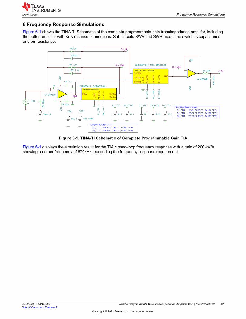
6 Frequency Response SimulationsFigure 6-1 shows the TINA-TI Schematic of the complete programmable gain transimpedance amplifer, including the buffer amplifier with Kelvin sense connections. Sub-circuits SWA and SWB model the switches capacitance and on-resistance.
VCC VEEVC
CV
EE
A1_CTRL
VC
C
VEE
B1_CTRL B2_CTRL B3_CTRL
B3
_C
TR
L
B2
_C
TR
L
B1
_C
TR
L
A1
_C
TR
L
A2
_C
TR
L
Vt
A2_CTRLC5 100n
C4 100n
RF2 2k
RF1 200k
C9
10
0p
Out_200k
Out_2k
CF1 1.6p
VCC 5 VEE -500m
CF2 50p
Vbias -3 A1 1
Out_Mux
C1
0 1
00
p
Vout2SWITCH-1-TO-3_OPA3S328
B3
_C
TR
L
L_
GN
D
B1
_C
TR
L
B2
_C
TR
L
OUTSB3
INSB
OUTSB2
OUTSB1
U2B SWITCH-1-TO-3_OPA3S328
B2 0 B3 0
-
++
U2 OPA328
-
++
U1 OPA328Vout1
IG1
SWA-1-to-2-OPA3S328
L_
GN
D
A2
_C
TR
L
A1
_C
TR
L
INSA OUTSA1
OUTSA2
U1B SWA-1-to-2-OPA3S328
R1 100
B1 1A2 0
Simplified Switch Model
A1_CTRL : 1V -A1 CLOSED 0V -A1 OPEN
A2_CTRL : 1V -A2 CLOSED 0V -A2 OPEN
Simplified Switch Model
B1_CTRL : 1V -B1 CLOSED 0V -B1 OPEN
B2_CTRL : 1V -B2 CLOSED 0V -B2 OPEN
B3_CTRL : 1V -B3 CLOSED 0V -B3 OPEN
Figure 6-1. TINA-TI Schematic of Complete Programmable Gain TIA
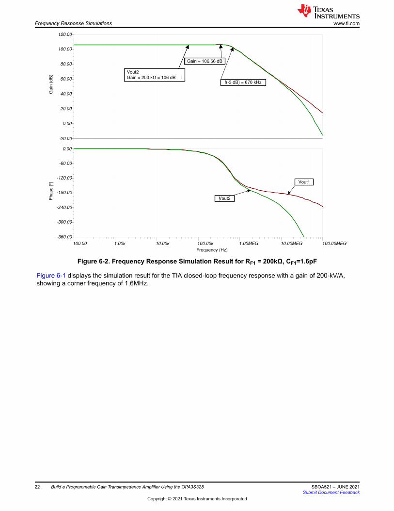
Figure 6-1 displays the simulation result for the TIA closed-loop frequency response with a gain of 200-kV/A, showing a corner frequency of 670kHz, exceeding the frequency response requirement.
www.ti.com Frequency Response Simulations
SBOA521 – JUNE 2021Submit Document Feedback
Build a Programmable Gain Transimpedance Amplifier Using the OPA3S328 21
Copyright © 2021 Texas Instruments Incorporated
T
Vout2
Gain = 200kOhm = 106dB
Gain = 106.56dB
f(-3dB) = 670kHz
Vout1
Vout2
Ga
in (
dB
)
-20.00
0.00
20.00
40.00
60.00
80.00
100.00
120.00
Frequency (Hz)
100.00 1.00k 10.00k 100.00k 1.00MEG 10.00MEG 100.00MEG
Ph
ase
[°]
-360.00
-300.00
-240.00
-180.00
-120.00
-60.00
0.00
Vout1
Vout2
f(-3 dB) = 670 kHz
Gain = 106.56 dB
Vout2
Gain = 200 N= 106 dB
Figure 6-2. Frequency Response Simulation Result for RF1 = 200kΩ, CF1=1.6pF
Figure 6-1 displays the simulation result for the TIA closed-loop frequency response with a gain of 200-kV/A, showing a corner frequency of 1.6MHz.
Frequency Response Simulations www.ti.com
22 Build a Programmable Gain Transimpedance Amplifier Using the OPA3S328 SBOA521 – JUNE 2021Submit Document Feedback
Copyright © 2021 Texas Instruments Incorporated
T
Vout2
Gain = 2kOhm = 66.02dB
Vout1
Vout2
Ga
in (
dB
)
-20.00
0.00
20.00
40.00
60.00
80.00
Frequency (Hz)
100.00 10.00k 100.00k 1.00MEG 10.00MEG 100.00MEG
Ph
ase
[°]
-360.00
-300.00
-240.00
-180.00
-120.00
-60.00
0.00
Vout2
Vout1
Vout2
Gain = 2 k = 66.02 dB
Vout2
f(-3 dB) = 1.74 MHz
1.00k
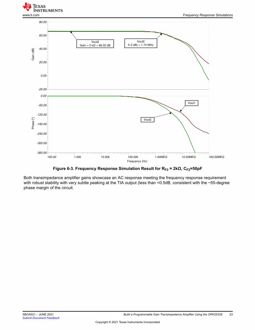
Figure 6-3. Frequency Response Simulation Result for RF2 = 2kΩ, CF2=50pF
Both transimpedance amplifier gains showcase an AC response meeting the frequency response requirement with robust stability with very subtle peaking at the TIA output (less than <0.5dB, consistent with the ~55-degree phase margin of the circuit.
www.ti.com Frequency Response Simulations
SBOA521 – JUNE 2021Submit Document Feedback
Build a Programmable Gain Transimpedance Amplifier Using the OPA3S328 23
Copyright © 2021 Texas Instruments Incorporated
7 ConclusionThe programmable gain TIA provides flexibility to measure a wide range of photodiode current while ensuring the amplifier remains inside its linear range. The OPA3S328 dual op-amp offers low input bias current, high DC precision performance, low noise, and high bandwidth, providing an optimal choice for transimpedance amplifier applications. The device incorporates two sets of low leakage, low capacitance, analog switches useful for the configuration of programmable gain amplifiers in a single device integrated solution.
The preceding discussion shows some of the design trade-offs when implementing programmable transimpedance amplifiers using analog switches, and a Kelvin-sense circuit topology to eliminate TIA gain error, gain error drift, and non-linearity due to the switch on-resistance. This document provides the information to assist the design engineer in implementing the programmable TIA design according to the specific application needs.
Conclusion www.ti.com
24 Build a Programmable Gain Transimpedance Amplifier Using the OPA3S328 SBOA521 – JUNE 2021Submit Document Feedback
Copyright © 2021 Texas Instruments Incorporated

8 References1. Texas Instruments Precision Hub, What op amp bandwidth do I need? (Transimpedance Amplifiers), May
2014, John Caldwell, Texas Instruments Blog: Part I, Part II and Part III.2. Texas Instruments, Compensate Transimpedance Amplifiers Intuitively application report.
www.ti.com References
SBOA521 – JUNE 2021Submit Document Feedback
Build a Programmable Gain Transimpedance Amplifier Using the OPA3S328 25
Copyright © 2021 Texas Instruments Incorporated

IMPORTANT NOTICE AND DISCLAIMERTI PROVIDES TECHNICAL AND RELIABILITY DATA (INCLUDING DATASHEETS), DESIGN RESOURCES (INCLUDING REFERENCEDESIGNS), APPLICATION OR OTHER DESIGN ADVICE, WEB TOOLS, SAFETY INFORMATION, AND OTHER RESOURCES “AS IS”AND WITH ALL FAULTS, AND DISCLAIMS ALL WARRANTIES, EXPRESS AND IMPLIED, INCLUDING WITHOUT LIMITATION ANYIMPLIED WARRANTIES OF MERCHANTABILITY, FITNESS FOR A PARTICULAR PURPOSE OR NON-INFRINGEMENT OF THIRDPARTY INTELLECTUAL PROPERTY RIGHTS.These resources are intended for skilled developers designing with TI products. You are solely responsible for (1) selecting the appropriateTI products for your application, (2) designing, validating and testing your application, and (3) ensuring your application meets applicablestandards, and any other safety, security, or other requirements. These resources are subject to change without notice. TI grants youpermission to use these resources only for development of an application that uses the TI products described in the resource. Otherreproduction and display of these resources is prohibited. No license is granted to any other TI intellectual property right or to any third partyintellectual property right. TI disclaims responsibility for, and you will fully indemnify TI and its representatives against, any claims, damages,costs, losses, and liabilities arising out of your use of these resources.TI’s products are provided subject to TI’s Terms of Sale (https:www.ti.com/legal/termsofsale.html) or other applicable terms available eitheron ti.com or provided in conjunction with such TI products. TI’s provision of these resources does not expand or otherwise alter TI’sapplicable warranties or warranty disclaimers for TI products.IMPORTANT NOTICE
Mailing Address: Texas Instruments, Post Office Box 655303, Dallas, Texas 75265Copyright © 2021, Texas Instruments Incorporated
Copyright © 2022 FDOKUMEN