Applications of Semiconductor Optical Amplifiers - UILIS ...
Upload
khangminh22Category
view
1download
0
http://www.cloudioe.com/resources.aspx

RF Power Amplifiers
http://www.cloudioe.com/resources.aspx

http://www.cloudioe.com/resources.aspx

RF Power Amplifiers
MARIAN K. KAZIMIERCZUKWright State University,
Dayton, Ohio, USA
A John Wiley and Sons, Ltd., Publication

This edition first published 2008 2008 John Wiley & Sons, Ltd
Registered officeJohn Wiley & Sons Ltd, The Atrium, Southern Gate, Chichester, West Sussex, PO19 8SQ, United Kingdom
For details of our global editorial offices, for customer services and for information about how to apply forpermission to reuse the copyright material in this book please see our website at www.wiley.com.
The right of the author to be identified as the author of this work has been asserted in accordance with theCopyright, Designs and Patents Act 1988.
All rights reserved. No part of this publication may be reproduced, stored in a retrieval system, or transmitted, inany form or by any means, electronic, mechanical, photocopying, recording or otherwise, except as permitted bythe UK Copyright, Designs and Patents Act 1988, without the prior permission of the publisher.
Wiley also publishes its books in a variety of electronic formats. Some content that appears in print may not beavailable in electronic books.
Designations used by companies to distinguish their products are often claimed as trademarks. All brand namesand product names used in this book are trade names, service marks, trademarks or registered trademarks oftheir respective owners. The publisher is not associated with any product or vendor mentioned in this book. Thispublication is designed to provide accurate and authoritative information in regard to the subject matter covered.It is sold on the understanding that the publisher is not engaged in rendering professional services. If professionaladvice or other expert assistance is required, the services of a competent professional should be sought.
Library of Congress Cataloging-in-Publication Data
Kazimierczuk, Marian.RF power amplifiers / Marian K. Kazimierczuk.
p. cm.Includes bibliographical references and index.ISBN 978-0-470-77946-0 (cloth)1. Power amplifiers. 2. Amplifiers, Radio frequency. I. Title.TK7871.58.P6K39 2008621.384′12 – dc22
2008032215
A catalogue record for this book is available from the British Library.
ISBN: 978-0-470-77946-0
Typeset by Laserwords Private Limited, Chennai, IndiaPrinted and bound in Great Britain by Antony Rowe Ltd, Chippenham, Wiltshire

To My Mother


Contents
Preface xvAbout the Author xviiList of Symbols xix
1 Introduction 11.1 Block Diagram of RF Power Amplifiers 11.2 Classes of Operation of RF Power Amplifiers 31.3 Parameters of RF Power Amplifiers 51.4 Conditions for 100 % Efficiency of Power Amplifiers 71.5 Conditions for Nonzero Output Power at 100 % Efficiency of
Power Amplifiers 101.6 Output Power of Class E ZVS Amplifier 111.7 Class E ZCS Amplifier 141.8 Propagation of Electromagnetic Waves 161.9 Frequency Spectrum 19
1.10 Duplexing 211.11 Multiple-access Techniques 211.12 Nonlinear Distortion in Transmitters 221.13 Harmonics of Carrier Frequency 231.14 Intermodulation 251.15 Dynamic Range of Power Amplifiers 271.16 Analog Modulation 28
1.16.1 Amplitude Modulation 291.16.2 Phase Modulation 321.16.3 Frequency Modulation 33
1.17 Digital Modulation 361.17.1 Amplitude-shift Keying 361.17.2 Phase-shift Keying 371.17.3 Frequency-shift Keying 38
1.18 Radars 391.19 Radio-frequency Identification 401.20 Summary 40

viii CONTENTS
1.21 References 421.22 Review Questions 421.23 Problems 43
2 Class A RF Power Amplifier 452.1 Introduction 452.2 Circuit of Class A RF Power Amplifier 452.3 Power MOSFET Characteristics 472.4 Waveforms of Class A RF Amplifier 522.5 Parameters of Class A RF Power Amplifier 562.6 Parallel-resonant Circuit 592.7 Power Losses and Efficiency of Parallel Resonant Circuit 622.8 Impedance Matching Circuits 662.9 Class A RF Linear Amplifier 69
2.9.1 Amplifier of Variable-envelope Signals 692.9.2 Amplifiers of Constant-envelope Signals 70
2.10 Summary 712.11 References 712.12 Review Questions 722.13 Problems 72
3 Class AB, B, and C RF Power Amplifiers 753.1 Introduction 753.2 Class B RF Power Amplifier 75
3.2.1 Circuit of Class B RF Power Amplifier 753.2.2 Waveforms of Class B Amplifier 763.2.3 Power Relationships in Class B Amplifier 783.2.4 Efficiency of Class B Amplifier 80
3.3 Class AB and C RF Power Amplifiers 823.3.1 Waveforms of Class AB and C RF Power Amplifiers 823.3.2 Power of the Class AB, B, and C Amplifiers 863.3.3 Efficiency of the Class AB, B, and C Amplifiers 883.3.4 Parameters of Class AB Amplifier at θ = 120 893.3.5 Parameters of Class C Amplifier at θ = 60 913.3.6 Parameters of Class C Amplifier at θ = 45 93
3.4 Push-pull Complementary Class AB, B, and C RF PowerAmplifiers 95
3.4.1 Circuit 953.4.2 Even Harmonic Cancellation in Push-pull Amplifiers 963.4.3 Power Relationships 973.4.4 Device Stresses 98
3.5 Transformer-coupled Class B Push-pull Amplifier 993.5.1 Waveforms 993.5.2 Power Relationships 1023.5.3 Device Stresses 102
3.6 Class AB, B, and C Amplifiers of Variable-envelope Signals 1053.7 Summary 1073.8 References 107

CONTENTS ix
3.9 Review Questions 1083.10 Problems 108
4 Class D RF Power Amplifiers 1094.1 Introduction 1094.2 Circuit Description 1104.3 Principle of Operation 114
4.3.1 Operation Below Resonance 1154.3.2 Operation Above Resonance 118
4.4 Topologies of Class D Voltage-source RF Power Amplifiers 1194.5 Analysis 121
4.5.1 Assumptions 1214.5.2 Series-resonant Circuit 1214.5.3 Input Impedance of Series-resonant Circuit 1244.5.4 Currents, Voltages, and Powers 1244.5.5 Current and Voltage Stresses 1294.5.6 Operation Under Short-circuit and Open-circuit
Conditions 1334.6 Voltage Transfer Function 1344.7 Bandwidth of Class D Amplifier 1364.8 Efficiency of Half-bridge Class D Power Amplifier 137
4.8.1 Conduction Losses 1374.8.2 Turn-on Switching Loss 1384.8.3 Turn-off Switching Loss 142
4.9 Design Example 1444.10 Class D RF Power Amplifier with Amplitude Modulation 1464.11 Transformer-coupled Push-pull Class D Voltage-switching RF
Power Amplifier 1474.11.1 Waveforms 1474.11.2 Power 1504.11.3 Current and Voltage Stresses 1504.11.4 Efficiency 150
4.12 Class D Full-bridge RF Power Amplifier 1524.12.1 Currents, Voltages, and Powers 1524.12.2 Efficiency of Full-bridge Class D RF Power Amplifier 1564.12.3 Operation Under Short-circuit and Open-circuit Conditions 1564.12.4 Voltage Transfer Function 157
4.13 Phase Control of Full-bridge Class D Power Amplifier 1584.14 Class D Current-switching RF Power Amplifier 160
4.14.1 Circuit and Waveforms 1604.14.2 Power 1624.14.3 Voltage and Current Stresses 1634.14.4 Efficiency 163
4.15 Transformer-coupled Push-pull Class D Current-switching RFPower Amplifier 165
4.15.1 Waveforms 1654.15.2 Power 1674.15.3 Device Stresses 1684.15.4 Efficiency 168

x CONTENTS
4.16 Bridge Class D Current-switching RF Power Amplifier 1714.17 Summary 1754.18 References 1764.19 Review Questions 1774.20 Problems 178
5 Class E RF Zero-voltage-switching RF PowerAmplifier 179
5.1 Introduction 1795.2 Circuit Description 1795.3 Circuit Operation 1815.4 ZVS and ZDS Operation of Class E Amplifier 1825.5 Suboptimum Operation 1845.6 Analysis 185
5.6.1 Assumptions 1855.6.2 Current and Voltage Waveforms 1855.6.3 Current and Voltage Stresses 1875.6.4 Input Impedance of the Series Resonant Circuit 1885.6.5 Output Power 1895.6.6 Component Values 189
5.7 Maximum Operating Frequency 1905.8 Choke Inductance 1915.9 Summary of Parameters at D = 0.5 191
5.10 Efficiency 1925.11 Design of Basic Class E Amplifier 1955.12 Impedance Matching Resonant Circuits 198
5.12.1 Tapped Capacitor Downward Impedance MatchingResonant Circuit π1a 199
5.12.2 Tapped Inductor Downward Impedance MatchingResonant Circuit π2a 202
5.12.3 Matching Resonant Circuit π1b 2055.12.4 Matching Resonant Circuit π2b 2085.12.5 Quarter-wavelength Impedance Inverters 211
5.13 Push-pull Class E ZVS RF Amplifier 2145.14 Class E ZVS RF Power Amplifier with Finite DC-feed Inductance 2165.15 Class E ZVS Amplifier with Parallel-series Resonant Circuit 2195.16 Class E ZVS Amplifier with Nonsinusoidal Output Voltage 2215.17 Class E ZVS Power Amplifier with Parallel Resonant Circuit 2265.18 Amplitude Modulation of Class E ZVS RF Power Amplifier 2315.19 Summary 2335.20 References 2345.21 Review Questions 2375.22 Problems 237
6 Class E Zero-current-switching RF Power Amplifier 2396.1 Introduction 2396.2 Circuit Description 2396.3 Principle of Operation 240

CONTENTS xi
6.4 Analysis 2436.4.1 Steady-state Current and Voltage Waveforms 2436.4.2 Peak Switch Current and Voltage 2456.4.3 Fundamental-frequency Components 245
6.5 Power Relationships 2476.6 Element Values of Load Network 2476.7 Design Example 2486.8 Summary 2496.9 References 249
6.10 Review Questions 2496.11 Problems 250
7 Class DE RF Power Amplifier 251
7.1 Introduction 2517.2 Analysis of Class DE RF Power Amplifier 2517.3 Components 2577.4 Device Stresses 2587.5 Design Equations 2587.6 Maximum Operating Frequency 2587.7 Class DE Amplifier with Only One Shunt Capacitor 2607.8 Components 2637.9 Cancellation of Nonlinearities of Transistor Output Capacitances 264
7.10 Summary 2647.11 References 2647.12 Review Questions 2657.13 Problems 265
8 Class F RF Power Amplifier 267
8.1 Introduction 2678.2 Class F RF Power Amplifier with Third Harmonic 268
8.2.1 Maximally Flat Class F3 Amplifier 2718.2.2 Maximum Drain Efficiency Class F3 Amplifier 276
8.3 Class F RF Power Amplifier with Third and Fifth Harmonics 2818.3.1 Maximally Flat Class F35 Amplifier 2818.3.2 Maximum Drain Efficiency Class F35 Amplifier 287
8.4 Class F RF Power Amplifier with Third, Fifth, and SeventhHarmonics 289
8.5 Class F RF Power Amplifier with Parallel-resonant Circuit andQuarter-wavelength Transmission Line 289
8.6 Class F RF Power Amplifier with Second Harmonic 2958.6.1 Maximally Flat Class F2 Amplifier 2958.6.2 Maximum Drain Efficiency Class F2 Amplifier 301
8.7 Class F RF Power Amplifier with Second and Fourth Harmonics 3058.7.1 Maximally Flat Class F24 Amplifier 3058.7.2 Maximum Drain Efficiency Class F24 Amplifier 310
8.8 Class F RF Power Amplifier with Second, Fourth, and SixthHarmonics 312
xii CONTENTS
8.9 Class F RF Power Amplifier with Series-resonant Circuit andQuarter-wavelength Transmission Line 313
8.10 Summary 3178.11 References 3198.12 Review Questions 3208.13 Problems 320
9 Linearization and Efficiency Improvement of RFPower Amplifiers 321
9.1 Introduction 3219.2 Predistortion 3229.3 Feedforward Linearization Technique 3249.4 Negative Feedback Linearization Technique 3269.5 Envelope Elimination and Restoration 3309.6 Envelope Tracking 3319.7 The Doherty Amplifier 332
9.7.1 Condition for High Efficiency Over Wide Power Range 3339.7.2 Impedance Modulation Concept 3349.7.3 Equivalent Circuit of the Doherty Amplifier 3359.7.4 Power and Efficiency of Doherty Amplifier 336
9.8 Outphasing Power Amplifier 3389.9 Summary 340
9.10 References 3419.11 Review Questions 3429.12 Problems 343
10 Integrated Inductors 34510.1 Introduction 34510.2 Skin Effect 34510.3 Resistance of Rectangular Trace 34810.4 Inductance of Straight Rectangular Trace 35010.5 Meander Inductors 35110.6 Inductance of Straight Round Conductor 35310.7 Inductance of Circular Round Wire Loop 35410.8 Inductance of Two-parallel Wire Loop 35410.9 Inductance of Rectangle of Round Wire 355
10.10 Inductance of Polygon Round Wire Loop 35510.11 Bondwire Inductors 35510.12 Single-turn Planar Inductors 35710.13 Inductance of Planar Square Loop 35910.14 Planar Spiral Inductors 359
10.14.1 Geometries of Planar Spiral Inductors 35910.14.2 Inductance of Square Planar Inductors 36110.14.3 Inductance of Hexagonal Spiral Inductors 36910.14.4 Inductance of Octagonal Spiral Inductors 37010.14.5 Inductance of Circular Spiral Inductors 371
10.15 Multimetal Spiral Inductors 37210.16 Planar Transformers 373

CONTENTS xiii
10.17 MEMS Inductors 37410.18 Inductance of Coaxial Cable 37610.19 Inductance of Two-wire Transmission Line 37610.20 Eddy Currents in Integrated Inductors 37610.21 Model of RF Integrated Inductors 37710.22 PCB Integrated Inductors 37810.23 Summary 37910.24 References 38010.25 Review Questions 38210.26 Problems 383
Appendices 385
Appendix A SPICE Model of Power MOSFETs 387
Appendix B Introduction to SPICE 391
Appendix C Introduction to MATLAB 395
Answers to Problems 399
Index 403


Preface
This book is about RF power amplifiers used in wireless communications and many other RFapplications. It is intended as a concept-oriented textbook at the senior and graduate levelsfor students majoring in electrical engineering, as well as a reference for practicing engineersin the area of RF power electronics. The purpose of the book is to provide foundationsfor RF power amplifiers, efficiency improvement, and linearization techniques. Class A, B,C, D, E, DE, and F RF power amplifiers are analyzed and design procedures are given.Impedance transformation is covered. Various linearization techniques are explored, suchas predistortion, feedforward, and negative feedback techniques. Efficiency improvementmethods are also studied, such as envelope elimination and restoration, envelope tracking,Doherty amplifier, and outphasing techniques. Integrated inductors are also studied.
The textbook assumes that the student is familiar with general circuit analysis techniques,semiconductor devices, linear systems, and electronic circuits. A communications course isalso very helpful.
I wish to express my sincere thanks to Simone Taylor, Publisher, Engineering Technology,Jo Bucknall, Assistant Editor, and Erica Peters, Content Editor. It has been a real pleasureworking with them. Last but not least, I wish to thank my family for the support.
I am pleased to express my gratitude to Nisha Das for the MATLAB figures. Theauthor would welcome and greatly appreciate suggestions and corrections from readers,for improvements in the technical content as well as the presentation style.
Marian K. Kazimierczuk


About the Author
Marian K. Kazimierczuk is Professor of Electrical Engineering at Wright State University,Dayton, Ohio, USA. He is the author of five books, over 130 journal papers, over 150conference papers, and seven patents. He is a Fellow of the IEEE and he received anOutstanding Teacher Award from the American Society for Engineering Education in 2008.His research interests are in the areas of RF power amplifiers, radio transmitters, powerelectronics, PWM dc-dc power converters, resonant dc-dc power converters, modeling andcontrols, semiconductor power devices, magnetic devices, and renewable energy sources.


List of Symbols
a Coil mean radiusAe Effective area of antennaAv voltage gainB Magnetic flux densityBW Bandwidthcp Output-power capability of amplifierC Resonant capacitanceCc Coupling capacitanceCds Drain-source capacitance of MOSFETCds(25V ) Drain-source capacitance of MOSFET at VDS = 25 VCf Filter capacitanceCfmin Minimum value of Cf
Cgd Gate-drain capacitance of MOSFETCgs Gate-source capacitance of MOSFETCiss MOSFET input capacitance at VDS = 0, Ciss = Cgs + Cgd
Coss MOSFET output capacitance at VGD = 0, Coss = Cgs + Cds
Cox Oxide capacitance per unit areaCout Transistor output capacitanceCrss MOSFET transfer capacitance, Crss = Cgd
CB Blocking capacitanced Coil inner diameterD Coil outer diameterE Electric field intensityf Operating frequency, switching frequencyfc Carrier frequencyfIF Intermediate frequencyfLO Local oscillator frequencyfm Modulating frequencyfo Resonant frequencyfp Frequency of pole of transfer functionfr Resonant frequency of L-C -R circuitfs Switching frequencygm Transconductance of transistor

xx RF POWER AMPLIFIERS
H Magnetic flux intensityh Trace thicknessi CurrentiC Capacitor currentID DC drain currentiD Large-signal drain currentid Small-signal drain currentiL Inductor currentio Ac output currentiS Switch currentIm Amplitude of current iIrms Rms value of iIDM Peak drain currentISM Peak current of switchJn Bessel’s function of first kind and n-th orderK MOSFET parameterkp Power gainl Trace length, Winding lengthL Resonant inductance, channel lengthLf Filter inductanceLfmin Minimum value of Lf
m Modulation indexmf Index of frequency modulationmp Index of phase modulationN Number of inductor turnsn Transformer turns ratiop Perimeter enclosed by coilPG Gate drive powerpr Power loss in resonant circuitPtf Average power loss due to current fall time tfPAM Power of AM signalPC Power of carrierPLS Power of lower sidebandPLoss Power lossPD Power dissipationPI Dc supply (input) powerPO Ac output powerPUS Power of upper sidebandpD (ωt) Instantaneous drain power lossQo Unloaded quality factor at foQoL Quality factor of inductorQL Loaded quality factor at for Total parasitic resistancerC ESR of filter capacitorrDS On-resistance of MOSFETR Overall resistance of amplifierRDC DC input resistance of AmplifierrG Gate resistanceRL Dc load resistanceRLmin Minimum value of RL

LIST OF SYMBOLS xxi
ro Ouput resistance of transistors Trace-to-trace spacingSi Current slopeSv Voltage slopeT Operating temperatureTHD Total harmonic distortionVA Channel-modulation voltagev VoltageVDS DC drain-source voltageVdsm Amplitude of small-signal drain-source voltagevDS Large-signal drain-source voltagevds Small-signal drain-source voltageVGS DC gate-source voltagevGS Large-signal gare-source voltageVgm Amplitude of small-signal gate-source voltagevgs Small-simal gate-source voltagevm Modulating voltagevc Carrier voltagevm Modulating voltagevo Ac output voltageVc Amplitude of carrier voltageVm Amplitude of modulating voltageVm Amplitude of voltageVn n-th harmonic of the output voltageVCm Amplitude of the voltage across capacitanceVDS DC drain-source voltagevDS Large-signal drain-source voltagevds Small-signal drain-source voltageVI DC supply (input) voltageVLm Amplitude of the voltage across inductanceVDSM Peak voltage of switchVrms Rms value of vVt Threshold voltage of MoSFETw Trace widthW Energy, channel widthX Imaginary part of ZZ Input impedance of resonant circuitZi Input impedance|Z | Magnitude of ZZo Characteristic impedance of resonant circuitαn Fourier coefficients of drain currentβ Gain of feedback networkδ Dirac impulse functionf Frequency deviationεox Oxide permittivityη Efficiency of amplifierηAV Average efficiencyηD Drain efficiencyηr Efficiency of resonant circuitηPAE Power-aided efficiency

xxii RF POWER AMPLIFIERS
λ Wavelength, channel length-modulation parameterµ0 Permeability of fee spaceµn Mobility of electronsµr Relative permeabilityρ Resistivityσ Conductivityξn Fourier coefficients of drain-source voltageγn Ratio Fourier coefficients of drain current Phase, angle, magnetic fluxθ Half of drain current conduction angle, mobility degration coefficientω Operating angular frequencyωc Carrier angular frequencyωm Modulating angular frequencyωo Resonant angular frequency

1Introduction
1.1 Block Diagram of RF Power Amplifiers
A power amplifier [1–15] is a key element to build a wireless communication systemsuccessfully. To minimize interference and spectral re-growth, transmitters must be linear.A block diagram of an RF power amplifier is shown in Figure 1.1. It consists of a transistor(MOSFET, MESFET, or BJT), output network, input network, and RF choke. In RF poweramplifiers, a transistor can be operated
• as a dependent-current source;
• as a switch;
• in overdriven mode (partially as a dependent source and partially as a switch).
Figure 1.2(a) shows a model of an RF power amplifier in which the transistor is operatedas a voltage- or current-dependent current source. When a MOSFET is operated as a depen-dent current source, the drain current waveform is determined by the gate-to-source voltagewaveform and the transistor operating point. The drain voltage waveform is determinedby the dependent current source and the load network impedance. When a MOSFET isoperated as a switch, the switch voltage is nearly zero when the switch is ON and the draincurrent is determined by the external circuit due to the switching action of the transistor.When the switch is OFF, the switch current is zero and the switch voltage is determined bythe external circuit response.
In order to operate the MOSFET as a dependent-current source, the transistor cannotenter the ohmic region. It must be operated in the active region, also called the pinch-off region or the saturation region. Therefore, the drain-to-source voltage vDS must bekept higher than the minimum value VDSmin , i.e., vDS > VDSmin = VGS − Vt , where Vt isthe transistor threshold voltage. When the transistor is operated as a dependent-currentsource, the magnitudes of the drain current iD and the drain-to-source voltage vDS arenearly proportional to the magnitude of the gate-to-source voltage vGS . Therefore, this type
RF Power Amplifiers Marian K. Kazimierczuk 2008 John Wiley & Sons, Ltd

2 RF POWER AMPLIFIERS
VI
+vo
Cc
RFCIIio
+vDS
iD
in
RL
OutputNetwork
+
vn
vs
+vGS~ Input
Network
PG
iGis PO
+
+ VI
Figure 1.1 Block diagram of RF power amplifier.
VI
+vO
Cc
RFCIIiO
+vDS
ID
in
RL
OutputNetwork
+
vn
rDS
R
(b)
VI
+vO
Cc
RFCIIiO
+vDS
iD
in
RL
OutputNetwork
+
vn
(a)
R
+ VI
+ VI
Figure 1.2 Modes of operation of transistor in RF power amplifiers. (a) Transistor as a dependentcurrent source. (b) Transistor as a switch.
of operation is suitable for linear power amplifiers. Amplitude linearity is important foramplitude-modulated (AM) signals.
Figure 1.2(b) shows a model of an RF power amplifier in which the transistor is operatedas a switch. To operate the MOSFET as a switch, the transistor cannot enter the active

INTRODUCTION 3
region, also called the pinch-off region. It must remain in the ohmic region when it is ON
and in the cutoff region when it is OFF. To maintain the MOSFET in the ohmic region, itis required that vDS < VGS − Vt . If the gate-to-source voltage vGS is increased at a givenload impedance, the amplitude of the drain-to-source voltage vDS will increase, causing thetransistor to operate initially in the active region and then in the ohmic region. When thetransistor is operated as a switch, the magnitudes of the drain current iD and the drain-to-source voltage vDS are independent of the magnitude of the gate-to-source voltage vGS . Inmost applications, the transistor operated as a switch is driven by a rectangular gate-to-source voltage vGS . A sinusoidal gate-to-source voltage VGS is used to drive a transistoras a switch at very high frequencies, where it is difficult to generate rectangular voltages.The reason to use the transistors as switches is to achieve high amplifier efficiency. Whenthe transistor conducts a high drain current iD , the drain-to-source voltage vDS is low vDS ,resulting in low power loss.
If the transistor is driven by sinusoidal voltage vGS of high amplitude, the transistor isoverdriven. In this case, it operates in the active region when the instantaneous values ofvGS are low and as a switch when the instantaneous values of vGS are high.
The main functions of the output network are:
• impedance transformation;
• harmonic suppression;
• filtering of the spectrum of a signal with bandwidth BW to avoid interference withcommunication signals in adjacent channels.
1.2 Classes of Operation of RF Power Amplifiers
The classification of RF power amplifiers with a transistor operated as a dependent-currentsource is based on the conduction angle 2θ of the drain current. Waveforms of the draincurrent iD of a transistor operated as a dependent-source in various classes of operationfor sinusoidal gate-to-source voltage vGS are shown in Figure 1.3. The operating points forvarious classes of operation are shown in Figure 1.4.
In Class A, the conduction angle 2θ is 360. The gate-to-source voltage vGS must behigher than the transistor threshold voltage Vt , i.e., vGS > Vt . This is accomplished bychoosing the dc component of the gate-to-source voltage VGS sufficiently greater thanthe threshold voltage of the transistor Vt such that VGS − Vgsm > Vt , where Vgsm is theamplitude of the ac component of vGS . The dc drain current ID must be greater than theamplitude of the ac component Im of the drain current iD . As a result, the transistor conductsduring the entire cycle.
In Class B, the conduction angle 2θ is 180. The dc component VGS of the gate-to-sourcevoltage vGS is equal to Vt and the drain bias current ID is zero. Therefore, the transistorconducts for only half of the cycle.
In Class AB, the conduction angle 2θ is between 180 and 360. The dc component ofthe gate-to-source voltage VGS is slightly above Vt and the transistor is biased at a smalldrain current ID . As the name suggests, Class AB is the intermediate class between ClassA and Class B.
In Class C, the conduction angle 2θ of the drain current is less than 180. The operatingpoint is located in the cutoff region because VGS < Vt . The drain bias current ID is zero.The transistor conducts for an interval less than half of the cycle.

4 RF POWER AMPLIFIERS
ID
iD
0π 2π 3π 4πωt
iD
0π 2π 3π 4πωt
iD
0π 2π 3π 4πωt
iD
0π 2π 3π 4πωt
(a) (b)
(c) (d)
Figure 1.3 Waveforms of the drain current iD in various classes of operation. (a) Class A.(b) Class B. (c) Class AB. (d) Class C.
A
BC
iD
AB
0 Vt VGS
(a)
A
B C
iD
AB
0 VDS
(b)
Figure 1.4 Operating points for Classes A, B, AB, and C.
Class A, AB, and B operations are used in audio and RF power amplifiers, whereasClass C is used only in RF power amplifiers.
The transistor is operated as a switch in Class D, E, and DE RF power amplifiers. InClass F, the transistor can be operated as either a dependent current source or a switch.

INTRODUCTION 5
1.3 Parameters of RF Power Amplifiers
The dc supply power of an amplifier is
PI = II VI . (1.1)
When the resonant frequency of the output network fo is equal to the operating frequencyf , the power delivered by the drain to the output network (the drain power) is given by
PDS = 1
2Im Vm = 1
2I 2mR = V 2
m
2R(1.2)
where Im is the amplitude of the fundamental component of the drain current iD , Vm isthe amplitude of the fundamental component of the drain-to-source voltage vDS , and R isthe input resistance of the output network at the fundamental frequency. If the resonantfrequency fo is not equal to the operating frequency f , the drain power of the fundamentalcomponent is given by
PDS = 1
2Im Vm cos φ = 1
2I 2m R cos φ = V 2
m cos φ
2R(1.3)
where φ is the phase shift between the fundamental components of the drain current andthe drain-to-source voltage reduced by π .
The power level is often referenced to 1 mW and is expressed as
P = 10 log[P (W)]
0.001(dBm) = −30 + 10 log[P (W)](dBW). (1.4)
A dBm value or dBW value represents an actual power, whereas a dB value represents aratio of power, such as the power gain.
The instantaneous drain power dissipation is
pD (ωt) = iD vDS . (1.5)
The drain power dissipation is
PD = 1
2π
∫ 2π
0pD d(ωt) = 1
2π
∫ 2π
0iD vDS d(ωt) = PI − PDS . (1.6)
The drain efficiency is
ηD = PDS
PI= PI − PD
PI= 1 − PD
PI. (1.7)
The gate-drive power is
PG = 1
2π
∫ 2π
0iG vGS d(ωt). (1.8)
For sinusoidal gate current and voltage,
PG = 1
2Igm Vgsm cos φG = RG I 2
gm
2(1.9)
where Igm is the amplitude of the gate current, Vgsm is the amplitude of the gate-to-sourcevoltage, RG is the gate resistance, and φG is the phase shift between the fundamentalcomponents of the gate current and the gate-to-source voltage.
The output power is
PO = 1
2Iom Vom = 1
2I 2om RL = V 2
om
2RL. (1.10)

6 RF POWER AMPLIFIERS
The power loss in the resonant output network is
Pr = PDS − PO . (1.11)
The efficiency of the resonant output network is
ηr = PO
PDS. (1.12)
The overall power loss on the output side of the amplifier is
PLoss = PI − PO = PD + Pr . (1.13)
The overall efficiency of the amplifier is
η = PO
PI= PO
PDS
PDS
PI= ηDηr . (1.14)
The average efficiency is
ηAV = PO(AV )
PI (AV )(1.15)
where PO(AV ) is the average output power and PI (AV ) is the average dc supply power overa specified period of time. The efficiency of power amplifiers in which transistors are oper-ated as dependent-current sources increases with the amplitude of the output voltage Vm . Itreaches the maximum value at the maximum amplitude of the output voltage, which cor-responds to the maximum output power. In practice, power amplifiers are usually operatedbelow the maximum output power. For example, the drain efficiency of the Class B poweramplifier is ηD = π/4 = 78.5 % at Vm = VI , but it decreases to ηD = π/8 = 39.27 % atVm = VI /2.
The power-added efficiency is the ratio of the difference between the output power andthe gate-drive power to the supply power:
ηPAE = Output power − Drive power
DC supply power= PO − PG
PI= PO
PI
(1 − 1
kp
)= η
(1 − 1
kp
).
(1.16)If kp = PO/PG = 1, ηPAE = 0. If kp 1, ηPAE ≈ η.
The output power capability is given by
cp = PO(max )
NIDM VDSM= ηPI
NIDM VDSM= 1
2N
(II
IDM
)(VI
VDSM
)
= 1
2N
(Im
II
)(II
IDM
)(Vm
VI
)(VI
VDSM
)(1.17)
where IDM is the maximum value of the instantaneous drain current iD , VDSM is the max-imum value of the instantaneous drain-to-source voltage vDS , and N is the number oftransistors in an amplifier, which are not connected in parallel or in series. For example, apush-pull amplifier has two transistors. The maximum output power of an amplifier with atransistor having the maximum ratings IDM and VDSM is
PO(max ) = cpIDM VDSM . (1.18)
As the output power capability cp increases, the maximum output power PO(max ) alsoincreases. The output power capability is useful for comparing different types or familiesof amplifiers.
Typically, the output thermal noise of power amplifiers should be below −130 dBm. Thisrequirement is to introduce negligible noise to the input of the low-noise amplifier (LNA)of the receiver.

INTRODUCTION 7
Example 1.1
An RF power amplifier has PO = 10 W, PI = 20 W, PG = 1 W. Find the efficiency, power-added efficiency, and power gain.
Solution. The efficiency of the power amplifier is
η = PO
PI= 10
20= 50 %. (1.19)
The power-added efficiency is
η = PO − PG
PI= 10 − 1
20= 45 %. (1.20)
The power gain is
kp = PO
PG= 10
1= 10 = 10 log(10) = 10 dB. (1.21)
1.4 Conditions for 100% Efficiency of PowerAmplifiers
The drain efficiency is given by
ηD = PDS
PI= 1 − PD
PI. (1.22)
The condition for achieving a drain efficiency of 100 % is
PD = 1
T
∫ T
0iD vDS dt = 0. (1.23)
For an NMOS, iD ≥ 0 and vDS ≥ 0 and for a PMOS, iD ≤ 0 and vDS ≤ 0. In this case, thecondition for achieving a drain efficiency of 100 % becomes
iD vDS = 0. (1.24)
Thus, the waveforms iD and vDS should be nonoverlapping for an efficiency of 100 %.Nonoverlapping waveforms iD and vDS are shown in Figure 1.5.
The drain efficiency of power amplifiers is less than 100 % for the following cases:
• The waveforms of iD > 0 and vDS > 0 are overlapping (e.g., like in a Class C amplifier).
• The waveforms of iD and vDS are adjacent, and the waveform vDS has a jump at t = toand the waveform iD contains an impulse Dirac function, as shown in Figure 1.6(a).
• The waveforms of iD and vDS are adjacent, and the waveform iD has a jump at t = toand the waveform vDS contains an impulse Dirac function, as shown in Figure 1.6(b).
For the case of Figure 1.6(a), an ideal switch is connected in parallel with a capacitorC . The switch is turned on at t = to , when the voltage vDS across the switch is nonzero.At t = to , this voltage can be described by
vDS (to) = 1
2
[lim
t→t−OvDS (t) + lim
t→t−o(t)
]= V
2. (1.25)

8 RF POWER AMPLIFIERS
t02T
iD
T
t02T
vDS
T
Figure 1.5 Nonoverlapping waveforms of drain current iD and drain-to-source voltage vDS .
At t = to , the drain current is given by
iD (to) = C V δ(t − to). (1.26)
Hence, the instantaneous power dissipation is
pD (t) = iD vDS =
12 C V 2δ(t − to) for t = to0 for t = to ,
(1.27)
resulting in the time average power dissipation
PD = 1
T
∫ T
0iD vDS dt = 1
2fC V 2 (1.28)
and the drain efficiency
ηD = 1 − PD
PI= 1 − fC V 2
2PI. (1.29)
In a real circuit, the switch has a small series resistance, and the current through the switchis an exponential function of time of finite peak value.
Example 1.2
An RF power amplifier has a step change in the drain-to-source voltage at the MOSFETturn-on VDS = 5 V, the transistor capacitance is C = 100 pF, the operating frequency isf = 2.4 GHz, and the dc supply power is PI = 5 W. Assume that all parasitic resistancesare zero. Find the efficiency of the power amplifier.
Solution. The switching power loss is
PD = 1
2fC V 2
DS = 1
2× 2.4 × 109 × 100 × 10−12 × 52 = 3 W. (1.30)

INTRODUCTION 9
Hence, the drain efficiency of the amplifier is
ηD = PO
PI= PI − PD
PI= 1 − PD
PI= 1 − 3
5= 40 %. (1.31)
For the amplifier of Figure 1.6(b), an ideal switch is connected in series with an inductorL. The switch is turned on at t = to , when the current iD through the switch is nonzero. Att = to , the switch current can be described by
iD (to ) = 1
2
[lim
t→t−oiD (t) + lim
t→t+oiD (t)
]= I
2. (1.32)
C
VI
iD +
vDS R
II RFC
OutputNetwork
t0
vDS
∆V
Tto
to t
iD
0 T
to)C∆Vδ(t
t0 Tto
pD(ωt)
PD
to)C∆V2δ(t12
fC∆V2
2
L
VI
iD +
vDS R
II RFC
OutputNetwork
t0
iD
∆I
Tto
to t
vDS
0 T
L∆Iδ(t
t0 Tto
pD(ωt)
PD
L∆I2δ(t to)12
fL∆I2
2
(a) (b)
to)
Figure 1.6 Waveforms of drain current iD and drain-to-source voltage vDS with delta Dirac func-tions. (a) Circuit with the switch in parallel with a capacitor. (b) Circuit with the switch in serieswith an inductor.

10 RF POWER AMPLIFIERS
At t = to , the drain current is given by
vDS (to) = LI δ(t − to). (1.33)
Hence, the instantaneous power dissipation is
pD (t) = iD vDS =
12 LI 2δ(t − to) for t = to0 for t = to ,
(1.34)
resulting in the time average power dissipation
PD = 1
T
∫ T
0iD vDS dt = 1
2fLI 2 (1.35)
and the drain efficiency
ηD = 1 − PD
PI= 1 − fLI 2
2PI. (1.36)
In reality, the switch in the off-state has a large parallel resistance and voltage with a finitepeak value developed across the switch.
1.5 Conditions for Nonzero Output Power at 100%Efficiency of Power Amplifiers
The drain current and drain-to-source voltage waveforms have fundamental limitations forsimultaneously achieving 100 % efficiency and PO > 0 [9, 10]. The drain current iD andthe drain-to-source voltage vDS can be represented by the Fourier series
iD = II +∞∑
n=1
idn = II +∞∑
n=1
Idn sin(nωt + ψn ) (1.37)
and
vDS = VI +∞∑
n=1
vdsn = VI +∞∑
n=1
Vdsn sin(nωt + ϑn ). (1.38)
The derivatives of these waveforms with respect to time are
i ′D = diD
dt= ω
∞∑n=1
nIdn cos(nωt + ψn ) (1.39)
and
v ′DS = dvDS
dt= ω
∞∑n=1
nVdsn cos(nωt + ϑn ). (1.40)
Hence, the average value of the product of the derivatives is
1
T
∫ T
0i ′D v ′
DS dt = −ω2
2
∞∑n=1
n2IdnVdsn cos φn = −ω2∞∑
n=1
n2Pdsn (1.41)
where φn = ϑn − ψn − π . Next,∞∑
n=1
n2Pdsn = − 1
4π2f
∫ T
0i ′D v ′
DS dt . (1.42)

INTRODUCTION 11
If the efficiency of the output network is ηn = 1 and the power at harmonic frequencies iszero, i.e., Pds2 = 0, Pds3 = 0, . . . , then
Pds1 = PO1 = − 1
4π2f
∫ T
0i ′D v ′
DS dt . (1.43)
For multipliers, if ηn = 1 and the power at the fundamental frequency and at harmonicfrequencies is zero except that of the n-th harmonic frequency, then the power at the n-thharmonic frequency is
Pdsn = POn = − 1
4π2n2
∫ T
0i ′D v ′
DS dt . (1.44)
If the output network is passive and linear, then
−π
2≤ φn ≤ π
2. (1.45)
In this case, the output power is nonzero
PO > 0 (1.46)
if
1
T
∫ T
0i ′D v ′
DS dt < 0. (1.47)
If the output network and the load are passive and linear and
1
T
∫ T
0i ′D v ′
DS dt = 0 (1.48)
then
PO = 0 (1.49)
for the following cases:
• The waveforms iD and vDS are nonoverlapping, as shown in Figure 1.5.
• The waveforms iD and vDS are adjacent and the derivatives at the joint time instants tjare i ′
D (tj ) = 0 and v ′DS (tj ) = 0, as shown in Figure 1.7(a).
• The waveforms iD and vDS are adjacent and the derivative i ′D (tj ) at the joint time instant
tj has a jump and v ′DS (tj ) = 0, or vice versa, as shown in Figure 1.7(b).
• The waveforms iD and vDS are adjacent and their both derivatives iD (tj ) and VDS (tj )have jumps at the joint time instant tj , as shown in Figure 1.7(c).
1.6 Output Power of Class E ZVS Amplifier
The Class E zero-voltage switching (ZVS) RF power amplifier is shown in Figure 1.8.Waveforms for the Class E amplifier under zero-voltage switching and zero-derivativeswitching (ZDS) conditions are shown in Figure 1.9. Ideally, the efficiency of this ampli-fier is 100 %. Waveforms for the Class E amplifier are shown in Figure 1.9. The draincurrent iD has a jump at t = to . Hence, the derivative of the drain current at t = to isgiven by
i ′D (to) = I δ(t − to ) (1.50)

12 RF POWER AMPLIFIERS
t0 T
0 tT
T t0
T t0
t0 T
t0 T
t0 T
0 tT
T t0
T t0
t0 T
t0 T
0 tT T t0 0 tT
(a) (c)(b)
iD
vDS
i ′Dv ′DS
v ′DS
i ′D
iD
vDS
i ′Dv ′DS
v ′DS
i ′D
iD
vDS
i ′Dv ′DS
v ′DS
i ′D
Figure 1.7 Waveforms of power amplifiers with PO = 0.
L
C1
C
VI
iD +
vDS R
II RFC
Figure 1.8 Class E ZVS power amplifier.

INTRODUCTION 13
t0
iD
∆I
Tto
to t
vDS
Sv
0 T
i ′D
t0 Tto
t0 Tto
∆Iδ(t to)Sv2
i ′Dv ′DS
∆Iδ(t to)
v ′DS
t0 Tto
Sv
Sv
2
Figure 1.9 Waveforms of Class E ZVS power amplifier.
and the derivative of the drain-to-source voltage at t = to is given by
v ′DS (to ) = 1
2
[lim
t→t−ov ′
DS (t) + limt→t+o
v ′DS (t)
]= Sv
2. (1.51)

14 RF POWER AMPLIFIERS
The output power of the Class E ZVS amplifier is
Pds = PO = − 1
4π2f
∫ T
0i ′D v ′
DS dt = − 1
4π2f
∫ T
0v ′
DS I δ(t − to) dt
= −ISv
8π2f
∫ T
0δ(t − to ) dt = −ISv
8π2f(1.52)
where I < 0. SinceI = −0.6988IDM (1.53)
andSv = 11.08fVDSM (1.54)
the output power is
PO = −ISv
8π2f= 0.0981IDM VDSM . (1.55)
Hence, the output power capability is
cp = PO
IDM VDSM= 0.0981. (1.56)
Example 1.3
A Class E ZVS RF power amplifier has a step change in the drain current at the MOSFETturn-off ID = −1 A, a slope of the drain-to-source voltage at the MOSFET turn-off Sv =11.08 × 10⁸ V/s, and the operating frequency is f = 1 MHz. Find the output power of theamplifier.
Solution. The output power of the power amplifier is
PO = −ISv
8π2f= −−1 × 11.08 × 108
8π2 × 106= 14.03 W. (1.57)
1.7 Class E ZCS Amplifier
The Class E zero-current switching (ZCS) RF power amplifier is depicted in Figure 1.10.Current and voltage waveforms under zero-current switching and zero-derivative switching(ZDS) conditions are shown in Figure 1.11. The efficiency of this amplifier with perfect
L C
VI R
L1
Figure 1.10 Class E ZCS power amplifier.

INTRODUCTION 15
t0
iD
∆V
Tto
to t
vDS
Si
Si
0 T
i ′D
t0 Tto
t0 Tto
∆Vδ(t to)Si2
i ′Dv ′DS
∆Vδ(t to)
v ′DS
t0 Tto
Si2
Figure 1.11 Waveforms of Class E ZCS power amplifier.
components and under ZCS condition is 100 %. The drain-to-source voltage vDS has a jumpat t = to . The derivative of the drain-to-source voltage at t = to is given by
v ′DS (to) = V δ(t − to ) (1.58)
and the derivative of the drain current at t = to is given by
i ′D (to) = 1
2
[lim
t→t−oi ′D (t) + lim
t→t+oi ′D (t)
]= Si
2. (1.59)

16 RF POWER AMPLIFIERS
The output power of the Class E ZCS amplifier is
Pds = PO = − 1
4π2f
∫ T
0i ′D v ′
DS dt = − 1
4π2f
∫ T
0i ′DV δ(t − to) dt
= −VSi
8π2f
∫ T
0δ(t − to) dt = −VSi
8π2f. (1.60)
Since
V = −0.6988VDSM (1.61)
and
Si = 11.08fIDM (1.62)
the output power is
PO = −VSi
8π2f= 0.0981IDM VDSM . (1.63)
Hence, the output power capability is
cp = PO
IDM VDSM= 0.0981. (1.64)
Example 1.4
A Class E ZCS RF power amplifier has a step change in the drain-to-source voltage wave-form at the MOSFET turn-on VDS = −100 V, a slope of the drain current at the MOSFETturn-on Si = 11.08 × 10³ V/s, and the operating frequency is f = 1 MHz. Find the outputpower of the amplifier.
Solution. The output power of the power amplifier is
PO = −VDS Si
8π2f= −−100 × 11.08 × 107
8π2 × 106= 140.320 W. (1.65)
1.8 Propagation of Electromagnetic Waves
An antenna is a device for radiating or receiving electromagnetic radio waves. A transmittingantenna converts an electrical signal into an electromagnetic wave. It is a transition structurebetween a guiding device (such as a transmission line) and free space. A receiving antennaconverts an electromagnetic wave into an electrical signal. The electromagnetic wave travelsat the speed of light in free space. The wavelength of an electromagnetic wave in free spaceis given by
λ = c
f(1.66)
where c = 3 × 10⁸ m/s is the velocity of light in free space.An isotropic antenna is a theoretical point antenna that radiates energy equally in all
directions with its power spread uniformly on the surface of a sphere. This results in a

INTRODUCTION 17
spherical wavefront. The uniform radiated power density at a distance r from a transmitterwith the output power PT is given by
p(r) = PT
4πr2. (1.67)
The power density is inversely proportional to the square of the distance r . The hypotheticalisotropic antenna is not practical, but is commonly used as a reference to compare with otherantennas. If the transmitting antenna has directivity in a particular direction and efficiency,the power density in that direction is increased by a factor called the antenna gain GT . Thepower density received by a receiving directive antenna is
pr (r) = GTPT
4πr2. (1.68)
The antenna efficiency is the ratio of the radiated power to the total power fed to theantenna.
A receiving antenna pointed in the direction of the radiated power gathers a portion of thepower that is proportional to its cross-sectional area. The antenna effective area is given by
Ae = GRλ2
4π(1.69)
where GR is the gain of the receiving antenna and λ is the free-space wavelength. Thus, thepower received by a receiving antenna is given by the Herald Friis formula for free-spacetransmission as
PREC = Aep(r) = GT GRPTλ2
(4πr)2= GT GRPT
(c
4πrfc
)2
. (1.70)
The received power is proportional to the gain of either antenna and inversely proportionalto r2. For example, the gain of the dish (parabolic) antenna is given by
GT = GR = 6
(D
λ
)2
= 6
(Dfcc
)2
(1.71)
where D is the mouth diameter of the primary reflector. For D = 3 m and f = 10 GHz,GT = GR = 60,000 = 47.8 dB.
The space loss is the loss due to spreading the RF energy as it propagates through freespace and is defined as
SL = PT
PREC=(
4πr
λ
)2
= 10 log
(PT
PREC
)= 20 log
(4πr
λ
). (1.72)
There are also other losses such as atmospheric loss, polarization mismatch loss, impedancemismatch loss, and pointing error denoted by Lsyst . Hence, the link equation is
PREC = Lsyst GT GRPT
(4π )2
(λ
r
)2
. (1.73)
The maximum distance between the transmitting and receiving antennas is
rmax = λ
4π
√Lsyst GT GR
(PT
PREC (min)
). (1.74)
Antennas are used to radiate the electromagnetic waves and transmit through the atmo-sphere. The radiation efficiency of antennas is high only if their dimensions are of the sameorder of magnitude as the wavelength of the carrier frequency fc . The length of antennas isusually λ/2 (a half-dipole antenna) or λ/4 (quarter-wave antenna) and it should be higher

18 RF POWER AMPLIFIERS
than λ/10. For example, the height of a quarter-wave antenna ha = 750 m at fc = 100 kHz,ha = 75 m at fc = 1 MHz, ha = 7.5 cm at fc = 1 GHz, and ha = 7.5 mm at fc = 10 GHz.
There are three groups of electromagnetic waves based on their propagation properties:
• ground waves (below 2 MHz);
• sky waves (2–30 MHz);
• line-of-sight waves, also called space waves or horizontal waves (above 30 MHz).
Wave propagation is illustrated in Figure 1.12. The ground waves travel parallel to theEarth’s surface and suffer little attenuation by smog, moisture, and other particles in thelower part of the atmosphere. Very high antennas are required for transmission of these low-frequency waves. The approximate transmission distance of ground waves is about 1600 km(1000 miles). Ground wave propagation is much better over water, especially salt water,than over a dry desert terrain. Ground wave propagation is the only way to communicateinto the ocean with submarines. Extremely low frequency (ELF) waves (30–300 Hz) areused to minimize the attenuation of the waves by sea water. A typical frequency is 100 Hz.
The sky waves leave the curved surface of the Earth and are refracted by the iono-sphere back to the surface of the Earth and therefore are capable of following the Earth’scurvature. The altitude of refraction of the sky waves varies from 50 to 400 km. The trans-mission distance between two transmitters is 4000 km. The ionosphere is a region abovethe atmosphere, where free ions and electrons exist in sufficient quantity to affect the wavepropagation. The ionization is caused by radiation from the Sun. It changes as the positionof a point on the Earth with respect to the Sun changes daily, monthly, and yearly. Aftersunset, the lowest layer of the ionosphere disappears because of rapid recombination ofits ions. The higher the frequency, the more difficult is the refracting (bending) process.Between the point where the ground wave is completely attenuated and the point wherethe first wave returns, no signal is received, resulting in the skip zone.
The line-of-sight waves follow straight lines. There are two types of line-of-sight waves:direct waves and ground reflected waves. The direct wave is by far the most widely used forpropagation between antennas. Signals of frequencies above HF band cannot be propagated
Earth
(a)
Earth
(b)
Ionosphere
Earth
(c)
Earth
(d)
Satellite Satellite
Figure 1.12 Electromagnetic wave propagation. (a) Ground wave propagation. (b) Sky wavepropagation. (c) Horizontal wave propagation. (d) Wave propagation in satellite communications.

INTRODUCTION 19
for long distances along the surface of the Earth. However, it is easy to propagate thesesignals through free space.
1.9 Frequency Spectrum
Table 1.1 gives the frequency spectrum. In the United States, the allocation of carrierfrequencies, bandwidths, and power levels of transmitted electromagnetic waves is regulatedby the Federal Communications Commission (FCC) for all nonmilitary applications. Thecommunication must occur in a certain part of the frequency spectrum. The carrier frequencyfc determines the channel frequency.
Low-frequency (LF) electromagnetic waves are propagated by the ground waves. Theyare used for long-range navigation, telegraphy, and submarine communication. The medium-frequency (MF) band contains the commercial radio band from 535 to 1705 kHz. This bandis used for radio transmission of amplitude-modulated (AM) signals to general audiences.The carrier frequencies are from 540 to 1700 kHz. For example, one carrier frequency isat fc = 550 kHz, and the next carrier frequency fc = 560 kHz. The modulation bandwidthis 5 kHz. The average power of local stations is from 0.1 to 1 kW. The average power ofregional stations is from 0.5 to 5 kW. The average power of clear stations is from 0.25 to50 kW. A radio receiver may receive power as low as of 10 pW, 1 µV/m, or 50 µV acrossa 300- antenna. Thus, the ratio of the output power of the transmitter to the input powerof the receiver is on the order of PT /PREC = 1015.
The range from 1705 to 2850 kHz is used for short-distance point-to-point communi-cations for services such as fire, police, ambulance, highway, forestry, and emergencyservices. The antennas in this band have reasonable height and radiation efficiency. Aero-nautical frequency range starts in MF range and ends in HF range. It is from 2850 to4063 kHz and is used for short-distance point-to-point communications and ground-air-ground communications. Aircraft flying scheduled routes are allocated specific channels.The high-frequency (HF) band contains the radio amateur band from 3.5 to 4 MHz in theUnited States. Other countries use this band for mobile and fixed services. High frequenciesare also used for long-distance point-to-point transoceanic ground-air-ground communica-tions. High frequencies are propagated by sky waves. The frequencies from 1.6 to 30 MHzare called short waves.
The very high frequency (VHF) band contains commercial FM radio and most TVchannels. The commercial frequency-modulated (FM) radio transmission is from 88 to
Table 1.1 Frequency spectrum.
Frequency range Band name Wavelength range
30–300 Hz Extremely Low Frequencies (ELF) 10 000–1000 km300–3000 Hz Voice Frequencies (VF) 1000–100 km
3–30 kHz Very Low Frequencies (VLF) 100–10 km30–300 kHz Low Frequencies (LF) 10–1 km0.3–3 MHz Medium Frequencies (MF) 1000–100 m
3–30 MHz High Frequencies (HF) 100–10 m30–300 MHz Very High Frequencies (VHF) 100–10 cm0.3–3 GHz Ultra High Frequencies (UHF) 100–10 cm
3–30 GHz Super High Frequencies (SHF) 10–1 cm30–300 GHz Extra High Frequencies (EHF) 10–1 mm

20 RF POWER AMPLIFIERS
Table 1.2 Broadcast frequency allocation.
Radio or TV Frequency range Channel spacing
AM Radio 535–1605 kHz 10 kHzTV (channels 2–6) 54–72 MHz 6 MHzTV 76–88 MHz 6 MHzFM Radio 88–108 MHz 200 kHzTV (channels 7–13) 174–216 MHz 6 MHzTV (channels 14–83) 470–806 MHz 6 MHz
Table 1.3 UHF and SHF frequency bands.
Band Name Frequency Range Units
L 1–2 GHzS 2–4 GHzC 4–8 GHzX 8–12.4 GHzKu 12.4–18 GHzK 18–26.5 GHzKu 26.5–40 GHz
108 MHz. The modulation bandwidth is 15 kHz. The average power is from 0.25 to 100 kW.The transmission distance of VHF TV signals is 160 km (100 miles).
TV channels for analog transmission range from 54 to 88 MHz and from 174 to 216 MHzin the VHF band and from 470 to 890 MHz in the ultrahigh-frequency (UHF) band. Theaverage power is 100 kW for the frequency range from 54 to 88 MHz and 316 kW forthe frequency range from 174 to 216 MHz. Broadcast frequency allocations are given inTable 1.2. The UHF and SHF frequency bands are given in Table 1.3. The cellular phonefrequency allocation is given in Table 1.4.
The superhigh frequency (SHF) band contains satellite communications channels. Satel-lites are placed in orbits. Typically, these orbits are 37 786 km in altitude above the equator.Each satellite illuminates about one-third of the Earth. Since the satellites maintain the sameposition relative to the Earth, they are placed in geostationary orbits. These geosynchronoussatellites are called GEO satellites. Each satellite contains a communication system that canreceive signals from the Earth or from another satellite and transmit the received signal backto the Earth or to another satellite. The system uses two carrier frequencies. The frequencyfor transmission from the Earth to the satellite (uplink) is 6 GHz and the transmissionfrom the satellite to the Earth (downlink) is at 4 GHz. The bandwidth of each channel is500 MHz. Directional antennas are used for radio transmission through free space. Satellitecommunications are used for TV and telephone transmission. The electronic circuits in thesatellite are powered by solar energy using solar cells that deliver the supply power of about1 kW. The combination of a transmitter and a receiver is called a transponder. A typicalsatellite has 12 to 24 transponders. Each transponder has a bandwidth of 36 MHz. The totaltime delay for GEO satellites is about 400 ms and the power of received signals is verylow. Therefore, a low Earth-orbit (LEO) satellite system was deployed for a mobile phonesystem. The orbits of LEO satellites are 500–1500 km above the Earth. These satellites arenot synchronized with the Earth’s rotation. The total delay time for LEO satellite is about250 ms.

INTRODUCTION 21
Table 1.4 Cellular phone frequency allocation.
System Frequency range Channel spacing Multiple access
AMPS M-B 824–849 MHz 30 MHz FDMAB-M 869–894 MHz 30 MHz
GSM-900 M-B 880–915 MHz 0.2 MHz TDMAB-M 915–990 MHz 0.2 MHz
GSM-1800 M-B 1710–1785 MHz 0.2 MHz TDMAB-M 1805–1880 MHz 0.2 MHz
PCS-1900 M-B 1850–1910 kHz 30 MHz TDMAB-M 1930–1990 kHz 30 MHz
IS-54 M-B 824–849 MHz 30 MHz TDMAB-M 869–894 MHz 30 MHz
IS-136 M-B 1850–1910 MHz 30 MHz TDMAB-M 1930–1990 MHz 30 MHz
IS-96 M-B 824–849 MHz 30 MHz CDMAB-M 869–894 MHz 30 MHz
IS-96 M-B 1850–1910 MHz 30 MHz CDMAB-M 1930–1990 MHz 30 MHz
Transmitter
Receiver
Switch
Figure 1.13 Block diagram of a transceiver.
1.10 Duplexing
In two-way communication, a transmitter and a receiver are used. The combination of atransmitter and a receiver is called a transceiver. A block diagram of the transceiver isshown in Figure 1.13. Duplexing techniques are used to allow for both users to transmitand receive signals. The most commonly used duplexing is called time-division duplexing(TDD). The same frequency channel is used for both transmitting and receiving signals,but the system transmits the signal for half of the time and receives for the other half.
1.11 Multiple-access Techniques
In multiple-access communications systems, information signals are sent simultaneouslyover the same channel. Cellular wireless mobile communications use the following multiple-access techniques to allow simultaneous communication among multiple transceivers:
• time-division multiple access (TDMA);

22 RF POWER AMPLIFIERS
• frequency-division multiple access (FDMA);
• code-division multiple access (CDMA).
In the TDMA, the same frequency band is used by all the users, but at different timeintervals. Each digitally coded signal is transmitted only during preselected time intervals,called the time slots TSL. During every time frame TF , each user has access to the channelfor a time slot TSL. The signals transmitted from different users do not interfere with eachother in the time domain.
In the FDMA, a frequency band is divided into many channels. The carrier frequencyfc determines the channel frequency. Each baseband signal is transmitted with a differentcarrier frequency. One channel is assigned to each user for a connection period. After theconnection is completed, the channel becomes available to other users. In FDMA, properfiltering must be carried out to provide channel selection. The signals transmitted fromdifferent users do not interfere with each other in the frequency domain.
In the CDMA, each user uses a different code (like a different language). CDMA allowsthe use of one carrier frequency. Each station uses a different binary sequence to modulatethe carrier. The signals transmitted from different users overlap in both the frequency andtime domains, but the messages are orthogonal.
There are several standards of cellular wireless communications:
• Advanced Mobile Phone Service (AMPS);
• Global System for Mobile Communications (GSM);
• CDMA wireless standard proposed by Qualcomm.
1.12 Nonlinear Distortion in Transmitters
Power amplifiers contain a transistor (MOSFET, MESFET, or BJT), which is a nonlineardevice operated under large-signal conditions. The drain current iD is a nonlinear functionof the gate-to-source voltage vGS . Therefore, power amplifiers produce components whichare not present in the amplifier input signal. The relationship between the output voltagevo and the input voltage vs of a ‘weakly nonlinear’ or a ‘nearly linear’ power amplifier,such as the Class A amplifier, is nonlinear vo = f (vs ). This relationship can be expandedinto Taylor’s power series around the operating point
vo = f (vs ) = VO(DC ) + a1vs + a2v 2s + a3v 3
s + a4v 4s + a5v 5
s + · · · (1.75)
Thus, the output voltage consists of an infinite number of nonlinear terms. Taylor’s powerseries takes into account only the amplitude relationships. Volterra’s power series includesboth the amplitude and phase relationships.
Nonlinearity of amplifiers produces two types of unwanted signals:
• harmonics of the carrier frequency;
• intermodulation products (IMPs).
Nonlinear distortion components may corrupt the desired signal. Harmonic distortion(HD) occurs when a single-frequency sinusoidal signal is applied to the power amplifierinput. Intermodulation distortion (IMD) occurs when two or more frequencies are applied

INTRODUCTION 23
at the power amplifier input. To evaluate the linearity of power amplifiers, we can use (1) asingle-tone test and (2) a two-tone test. In a single-tone test, a sinusoidal voltage sourceis used to drive a power amplifier. In a two-tone test, two sinusoidal sources connected inseries are used as a driver of a power amplifier. The first test will produce harmonics andthe second test will produce both harmonics and intermodulation products (IMPs).
1.13 Harmonics of Carrier Frequency
To investigate the process of generation of harmonics, let us assume that a power amplifieris driven by a single-tone excitation in the form of a sinusoidal voltage
vs (t) = Vm cos ωt . (1.76)
To gain an insight into generation of harmonics by a nonlinear transmitter, consider anexample of a memoryless time-invariant power amplifier described by a third-order poly-nomial
vo(t) = a1vs (t) + a2v 2s (t) + a3v 3
s (t). (1.77)
The output voltage of the transmitter is given by
vo(t) = a1Vm cos ωt + a2V 2m cos2 ωt + a3V 3
m cos3 ωt
= a1Vm cos ωt + 1
2a2V 2
m (1 + cos 2ωt) + 1
4a3Vm (3 cos ωt + cos 3ωt)
= 1
2a2V 2
m +(
a1Vm + 3
4a3V 3
m
)cos ωt + 1
2a2V 2
m cos 2ωt + 1
4a3V 3
m cos 3ωt . (1.78)
Thus, the output voltage of the power amplifier contains the fundamental components of thecarrier frequency f1 = fc and harmonics 2f1 = 2fc and 3f1 = 3fc , as shown in Figure 1.14.The amplitude of the n-th harmonic is proportional to V n
m . The harmonics may interferewith other communication channels and must be filtered out to an acceptable level.
Harmonics are always integer multiples of the fundamental frequency. Therefore, theharmonic frequencies of the transmitter output signal with carrer frequency fc are given by
fn = nfc . (1.79)
f1 f
f1 2f1 3f1 f
(a)
(b)
Figure 1.14 Spectrum of the input and output voltages of power amplifiers due to harmonics.(a) Spectrum of the input voltage. (b) Spectrum of the output voltage due to harmonics.

24 RF POWER AMPLIFIERS
where n = 2, 3, 4, . . . is an integer. If a harmonic signal of a sufficiently large amplitude fallswithin the bandwidth of a nearby receiver, it may cause interference with the reception andcannot be filtered out in the receiver. The harmonics should be filtered out in the transmitterin its bandpass output network. For example, the output network of a transmitter may offer37-dB second-harmonic suppression and 55-dB third-harmonic suppression.
Harmonic distortion is defined as the ratio of the amplitude of the n-th harmonic Vn tothe amplitude of the fundamental V1
HDn = Vn
V1= 20 log
(Vn
V1
)(dB). (1.80)
The distortion by the second harmonic is given by
HD2 = V2
V1=
1
2a2Vm
a1Vm + 3
4a3V 3
m
= a2Vm
2
(a1 + 3
4V 2
m
) . (1.81)
For a1 3a3V 2m/4,
HD2 ≈ a2Vm
2a1. (1.82)
The second harmonic distortion HD2 is proportional to the input voltage amplitude Vm .The distortion by the third harmonic is given by
HD3 = V3
V1=
1
4a3V 3
m
a1Vm + 3
4a3V 3
m
= a3V 2m
4a1 + 3a3V 2m
. (1.83)
For a1 3a3V 2m/4,
HD3 ≈ a3V 2m
4a1. (1.84)
The third-harmonic distortion HD3 is proportional to V 2m . Usually, the amplitudes of har-
monics should be −50 to −70 dB below the amplitude of the carrier.The ratio of the power of an n-th harmonic Pn to the power of the carrier Pc is
HDn = Pn
Pc= 10
Pn
Pc(dBc). (1.85)
The term ‘dBc’ refers to ratio of the power of a spectral distortion component to the powerof the carrer.
The harmonic content in a waveform is described by the total harmonic distortion (THD)defined as
THD =√
P2 + P3 + P4 + · · ·P1
=
√√√√√√√V 2
2
2R+ V 2
3
2R+ V 2
4
2R+ · · ·
V 21
2R
=√
V 22 + V 2
3 + V 24 + · · ·
V 21
=√
HD22 + HD2
3 + HD24 + · · · . (1.86)
Higher harmonics (n ≥ 2) are distortion terms.

INTRODUCTION 25
1.14 Intermodulation
Intermodulation occurs when two or more signals of different frequencies are applied to theinput of a nonlinear circuit, such as a nonlinear RF transmitter. This results in mixing thecomponents of different frequencies. Therefore, the output signal contains components withadditional frequencies, called intromodulation products. The frequencies of the intermod-ulation products are either the sums or the differences of the frequencies of input signalsand their harmonics. For a two-frequency input excitation at frequencies f1 and f2, thefrequencies of the output signal components are given by
fIM = nf1 ± mf2 (1.87)
where n = 0, 1, 2, 3, . . . and m = 0, 1, 2, 3, . . . are integers. The order of an intermodulationproduct for a two-tone signal is the sum of the absolute values of coefficients n and ngiven by
kIMP = n + m. (1.88)
If the intermodulation products of sufficiently large amplitudes fall within the bandwidth ofa receiver, they will degrade the reception quality. For example, 2f1 + f2, 2f1 − f2, 2f2 + f1,and 2f2 − f1 are the third-order intermodulation products. The third-order intermodulationproducts usually have components in the system bandwidth. In contrast, the second-orderharmonics 2f1 and 2f2, and the second-order intermodulation products f1 + f2 and f1 − f2are generally out of the system passband and are therefore not a serious problem.
A two-tone excitation test is used to evaluate intermodulation distortion of power ampli-fiers. In this test, the input voltage of a power amplifier is given by
vs (t) = Vm1 cos ω1t + Vm2 cos ω2t . (1.89)
If the power amplifier is a memoryless time-invariant circuit described by a third-orderpolynomial, the output voltage is given by
vo(t) = a1vs (t) + a2v 2s (t) + a3v 3
s (t)
= a1Vm1 cos ω1t + a1Vm2 cos ω2t + a2(Vm2 cos ω1t + Vm2 cos ω2t)2
+ a3(Vm1 cos ω1t + Vm2 cos ω2t)3
= a1Vm1 cos ω1t + a1Vm2 cos ω2t + a2V 2m1 cos2 ω1t + 2a2Vm1Vm2 cos ω1t cos ω2t
+ a2V 2m2 cos ω2t
+ a3V 3m1 cos3 ω1t + 3a3V 2
m1Vm2 cos2 ω1t cos ω2t + 3a3Vm1V 2m2 cos ω1t cos2 ω2t
+ a3V 3m2 cos3 ω2t . (1.90)
Thus,
vo =(
a1Vm1 + 3
2a3Vm1V 2
m2 + 3
4a3V 3
m1
)cos ω1t
+(
a1Vm2 + 3
2a3Vm2V 2
m1 + 3
4V 3
m2
)cos ω2t
+ a2Vm1Vm2 cos(ω2 − ω1)t + a2Vm1Vm2 cos(ω1 + ω2)t

26 RF POWER AMPLIFIERS
+ 3
4a3V 2
m1Vm2 cos(2ω1 − ω2)t + 3
4a3V 2
m1Vm2 cos(2ω1 + ω2)t
+ 3
4a3Vm1V 2
m2 cos(2ω2 − ω1)t + 3
4a3Vm1V 2
m2 cos(2ω2 + ω1)t + · · · . (1.91)
The output voltage contains:
• fundamental components f1 and f2;
• harmonics of the fundamental components 2f1, 2f2 3f1, 3f2, . . .;
• intermodulation products f2 − f1, f1 + f2, 2f1 − f2, 2f2 − f1, 2f1 + f2, 2f2 + f1, 3f1 − 2f2,3f2 − 2f1, . . . .
The spectrum of the two-tone input voltage of equal amplitudes and several componentsof the spectrum of the output voltage are depicted in Figure 1.15. If the difference betweenf2 and f1 is small, the intermodulation products appear in the close vicinity of f1 and f2.The third-order intromodulation products, which are at 2f1 − f2 and 2f2 − f1, are of themost interest because they are the closest to the fundamental components. The frequencydifference of the IM product at 2f1 − f2 from the fundamental component at f1 is
f = f1 − (2f1 − f2) = f2 − f1. (1.92)
The frequency difference of the IM product at 2f2 − f1 from the fundamental component atf2 is
f = (2f2 − f1) − f2 = f2 − f1. (1.93)
For example, if f1 = 800 kHz and f2 = 900 kHz, then the IMPs of particular interest are2f1 − f2 = 2 × 800 − 900 = 700 MHz and 2f2 − f1 = 2 × 900 − 800 = 1000 MHz. To filterout the unwanted components, filters with a very narrow bandwidth are required.
Assuming that Vm1 = Vm2 = Vm , the amplitudes of the third-order intermodulation prod-uct are
V2f2−f1 = V2f1−f2 = 3
4a3V 2
m . (1.94)
f1 f2 f
2f1 f2 f1 2f2 f1f2 f
(a)
(b)
IDM
Figure 1.15 Spectrum of the input and output voltages in power amplifiers due to intermodulation.(a) Spectrum of the input voltage. (b) Several components of the spectrum of the output voltage dueto intermodulation.

INTRODUCTION 27
Assuming that Vm1 = Vm2 = Vm and a3 a1, The third-order intermodulation distortionby the IMP component at 2f1 ± f2 or the IMP component at 2f2 ± f1 is given by
IM3 = V2f2−f1
Vf2
=3
4a3V 3
m(a1 + 9
4a3
)Vm
≈3
4a3V 3
m
a1Vm= 3
4
(a3
a1
)V 2
m . (1.95)
As Vm is increased, the amplitudes of the fundamental components Vf1 and Vf2 are directlyproportional to Vm , whereas the amplitudes of the third-order IM products V2f1−f2 andV2f2−f1 are proportional to Vm . Therefore, the amplitudes of the IM products increase threetimes faster than the amplitudes of the fundamentals and have an intersection point. If theamplitudes are drawn on a log-log scale, they are linear functions of Vm .
1.15 Dynamic Range of Power Amplifiers
Figure 1.16 shows the desired output power PO (f2) and the undesired third-order inter-modulation product output power PO (2f2 − f1) as functions of the input power Pi on alog-log scale. This characteristic exhibits a linear region and a nonlinear region. As theinput power Pi increases, the output power reaches saturation, causing power gain com-pression. The point at which the power gain of the nonlinear amplifier deviates from thefictitious ideal linear amplifier by 1 dB is called the 1-dB compression point. It is used as ameasure of the power handling capability of the power amplifier. The output power at the1-dB compression point is given by
PO(1dB) (dBm) = A1dB + Pi (1dB) (dBm) = Ao(1dB) − 1 dB + Pi (1dB) (dBm) (1.96)
where Ao is the power gain of an ideal linear amplifier and A1dB is the power gain at the1-dB compression point.
The dynamic range of a power amplifier is the region where the amplifier has a linearpower gain. It is defined as the difference between the output power PO(1dB) and theminimum detectable power POmin
dR = PO(1dB) − POmin (1.97)
IMD
1dB PO (f2)
PO (f2) PO (2f2PO (2f2
IPO
PO (1dB)
POmin
0Pi (1dB) Pi
dR
f1)f1)
Figure 1.16 Output power PO (f2) and PO (2f2 − f1) as functions of input power Pi of poweramplifier.

28 RF POWER AMPLIFIERS
where the minimum detectable power POmin is defined as an output power level x dB abovethe input noise power level POn , usually x = 3 dB.
In a linear region of the amplifier characteristic, the desired output power PO (f2) isproportional to the input power Pi , e.g., PO (f2) = aPi . Assume that the third-order inter-modulation product output power PO (2f2 − f1) increases proportionally to the third power,e.g., PO (2f2 − f1) = (a/8)3Pi . Projecting the linear region of PO (f2) and PO (2f2 − f1) resultsin an intersection point called the intercept point (IP), as shown in Figure 1.16, where theoutput power at the IP point is denoted by IPO .
The intermodulation product is the difference between the desired output power PO (f2)and the undesired output power of the intermodulation component PO (2f2 − f1) of a poweramplifier
IMD (dB) = PO (f2) (dBm) − PO (2f2 − f1) (dBm). (1.98)
1.16 Analog Modulation
The function of a communications system is to transfer information from one point toanother through a communication link. Block diagrams of a typical communication systemdepicted in Figure 1.17. It consists of a transmitter whose block diagram is shown inFigure 1.17(a) and a receiver whose block diagram is shown shown in in Figure 1.17(b).In a transmitting system, a radio-frequency signal is generated, amplified, modulated, andapplied to the antenna. A local oscillator generates a signal with a frequency fLO . The signalswith an intermediate frequency fIF and the local-oscillation frequency fLO are applied to amixer. The frequency of the output signal of the mixer and a bandpass filter is increased(up-conversion) from the intermediate frequency to a carrier frequency
fc = fLO + fIF . (1.99)
BasebandFilter X
LO
fLO = 900 MHz
AntennaMixer
PAfIF = 400 MHz
ADC + DSPModulation
(a)
fc = 900 MHzFilter
Filter X
LO
fLO = 500 MHz
AntennaMixer
fIF = 400 MHzfc = 900 MHz DAC + DSP+
DemodulationLNA Filter
(b)
fc = 900 MHz
Figure 1.17 (a) Block diagram of a transmitter. (b) Block diagram of a receiver.

INTRODUCTION 29
The RF current flows through the antenna and produces electromagnetic waves. Antennasproduce or collect electromagnetic energy. The transmitted signal is received by the antenna,amplified by a low-noise amplifier (LNA), and applied to a mixer. The frequency of theoutput signal of the mixer and a bandpass filter is reduced (down-conversion) from thecarrier frequency to an intermediate frequency
fIF = fc − fLO . (1.100)
The most important parameters of a transmitter are as follows:
• spectral efficiency;
• power efficiency;
• signal quality in the presence of noise and interference.
A ‘baseband’ signal (modulating signal or information signal) has a nonzero spectrumin the vicinity of f = 0 and negligible elsewhere. For example, a voice signal generatedby a microphone or a video signal generated by a TV camera are baseband signals. Themodulating signal may consist of many, e.g., 24 multiplexed telephone channels. In RFsystems with analog modulation, the carrier is modulated by an analog baseband signal.The frequency bandwidth occupied by the baseband signal is called the baseband. Themodulated signal consists of components with much higher frequencies than the highestbaseband frequency. The modulated signal is an RF signal. It consists of components whosefrequencies are very close to the frequency of the carrier.
RF modulated signals can be divided into two groups:
• variable-envelope signals;
• constant-envelope signals.
Modulation is the process of placing an information band around a high-frequency carrierfor transmission. Modulation conveys information by changing some aspects of a car-rier signal in response to a modulating signal. In general, a modulated output voltage isgiven by
vo(t) = A(t) cos[ωc t + θ (t)] (1.101)
where A(t) is the amplitude of the voltage, fc is the carrier frequency, and θ (t) is the phaseof the carrier. If the amplitude of vo is varied, it is called amplitude modulation (AM). Ifthe frequency of vo is varied, it is called frequency modulation (FM). If the phase of vo isvaried, it is called phase modulation (PM).
1.16.1 Amplitude Modulation
In amplitude modulation, the carrier envelope is varied by the modulating signal vm (t). Asingle-frequency modulating voltage is given by
vm (t) = Vm cos ωmt . (1.102)
The carrier voltage is
vc = Vc cos ωc t . (1.103)

30 RF POWER AMPLIFIERS
The amplitude-modulated (AM) voltage is
vo(t) = V (t) cos ωc t = [Vc + vm (t)] cos ωc t = (Vc + Vm cos ωmt) cos ωct
= Vc
(1 + Vm
Vccos ωmt
)cos ωct = Vc (1 + m cos ωmt) cos ωct (1.104)
where the modulation index is
m = Vm
Vc≤ 1. (1.105)
Applying the trigonometric identity,
cos ωc t cos ωm t = 12 [cos(ωc − ωm )t + cos(ωc + ωm )t] (1.106)
we can express vo as
vo = Vc cos ωc t + mVc
2cos(ωc − ωm )t + mVc
2cos(ωc + ωm )t]. (1.107)
The AM voltage modulated by a pure sine wave consists of carrier at fc , component atfc − fm , and component at fc + fm . The AM waveform consists of (1) the carrier componentat fc , (2) the lower side component at fc − fm , and (3) the upper side component at fc + fm .If a band of frequencies is used as a modulating signal, we obtain the lower side band andthe upper side band. A phasor diagram for amplitude modulation by a single-modulatingfrequency is shown in Figure 1.18.
The bandwidth of an AM signal is given by
BWAM = (fc + fm ) − (fc − fm ) = 2fm . (1.108)
The frequency range of voice from 100 to 3000 Hz contains about 95 % of energy. Thecarrier frequency fc is much higher than fm(max ), e.g., fc/fm(max ) = 200.
The power of the carrier is
PC = V 2c
2R. (1.109)
The power of the lower sideband PLS is equal to the power of the upper sideband PUS
PLS = PUS = m2V 2c
8R= m2
4PC . (1.110)
The total transmitted power of the AM signal is given by
PAM = PC + PLS + PUS =(
1 + m2
4+ m2
4
)PC =
(1 + m2
2
)PC . (1.111)
For m = 1, the total power is
PAMmax = PC + PLS + PUS =(
1 + 1
4+ 1
4
)PC = 3
2PC . (1.112)
Vc
ωm
ωm
Figure 1.18 Phasor diagram for amplitude modulation by a single modulating frequency.

INTRODUCTION 31
vi0
vo
t0
vo
vi0
t
Q
Figure 1.19 Amplification of AM signal by linear power amplifier.
A high-power AM voltage can be generated by the following methods:
• AM signal amplification using linear power amplifiers;
• drain amplitude modulation;
• gate-to-source bias operating point modulation.
Variable-envelope signals, such as AM signals, usually require linear power amplifiers.Figure 1.19 shows the amplification process of an AM signal by a linear power amplifier.In this case, the carrier and the sidebands are amplified by a linear amplifier. The drainAM signal can be generated by connecting a modulating voltage source in series with thedrain dc voltage supply VI . When the MOSFET is operated as a current source like inClass C amplifiers, it should be driven into the ohmic region. If the transistor is operatedas a switch, the amplitude of the output voltage is proportional to the supply voltage and ahigh-fidelity AM signal is achieved. However, the modulating signal vm must be amplifiedto a high power level before it is applied to modulate the supply voltage.
AM is used in commercial radio broadcasting and to transmit the video informationin analog TV. Variable-envelope signals are also used in modern wireless communicationsystems.
Quadrature amplitude modulation (QAM) is a modulation method, which is based onmodulating the amplitude of two carrier sinusoidal waves. The two waves are out of phasewith each other by 90 and therefore are called quadrature carriers. The QAM signal isexpressed as
vQAM = I (t) cos ωc t + Q(t) sin ωct (1.113)
where I (t) and Q(t) are modulating signals. The received signal can be demodulated bymultiplying the modulated signal vQAM by a cosine wave of carrier frequency fc
vDEM = vQAM cos ωct = I (t) cos ωct cos ωct + Q(t) sin ωct cos ωct
= 1
2I (t) + 1
2[I (t) cos(2ωct) + Q(t) sin(2ωc t)]. (1.114)
A low-pass filter removes the 2fc components, leaving only the I (t) term, which is unef-fected by Q(t). On the other hand, if the modulated signal vQAM is multiplied by a sinewave, and transmitted through a low-pass filter, one obtains Q(t).

32 RF POWER AMPLIFIERS
1.16.2 Phase Modulation
The output voltage with angle modulation is described by
vo = Vc cos[ωc t + θ (t)] = Vc cos φ(t) (1.115)
where the instantaneous phase is
φ(t) = ωct + θ (t) (1.116)
and the instantaneous angular frequency is
ω(t) = dφ(t)
dt= ωc + dθ (t)
dt. (1.117)
Depending on the relationship between θ (t) and vm (t), the angle modulation can be cate-gorized as:
• phase modulation (PM);
• frequency modulation (FM).
In PM systems, the phase of the carrier is changed by the modulating signal vm (t). InFM systems, the frequency of the carrier is changed by the modulating signal vm (t). Theangle modulated systems are inherently immune to amplitude fluctuations due to noise.In addition to the high degree of noise immunity, they require less RF power becausethe transmitter output power contains only the power of the carrier. Therefore, PM andFM systems are suitable for high-fidelity music broadcasting and for mobile radio wirelesscommunications. However, the bandwidth of an angle-modulated signal is much wider thanthat of an amplitude-modulated signal.
The modulating voltage, also called the message signal, is expressed as
vm (t) = Vm sin ωmt . (1.118)
The phase of PM signal is given by
θ (t) = kpvm (t) = kpVm sin ωmt = mp sin ωmt . (1.119)
Hence, the phase-modulated output voltage is
vo = Vc cos[ωc t + kpvm (t)] = Vc cos(ωct + kpVm sin ωmt) = Vc cos(ωc t + mp sin ωmt)
= Vc cos(ωc t + φ sin ωmt) = Vc cos φ(t) (1.120)
where the index of phase modulation is the maximum phase shift caused by the modulatingvoltage Vm .
mp = kpVm = φ. (1.121)
Hence, the maximum phase modulation is
φmax = kpVm(max ). (1.122)
The instantaneous frequency is
ω(t) = dφ(t)
dt= ωc + dθ (t)
dt= ωc + kpVmωm cos ωmt . (1.123)
Thus, the phase change results in a frequency change. The frequency deviation is
f = fmax − fc = fc + kpVm fm − fc = kpVm fm = mpfm . (1.124)
The frequency deviation f is directly proportional to the modulating frequency fm . Figure1.20 shows plots of the frequency modulation f as functions of the modulating frequencyfm and the amplitude of the modulating voltage Vm .

INTRODUCTION 33
∆f FM
PM PMandFM
fm
(a) (b)
Vm
∆f
Figure 1.20 (a) Frequency deviation f as a function of the modulating frequency fm .(b) Frequency deviation f as a function of the modulating voltage Vm .
1.16.3 Frequency Modulation
The modulating voltage is
vm (t) = Vm cos ωmt . (1.125)
The derivative of the phase is
dθ (t)
dt= 2πkf vm (t). (1.126)
Thus, the phase is
θ (t) = 2π
∫kf vm (t) dt = kf Vm
∫cos ωmt dt = kf Vm
fmsin ωmt . (1.127)
The frequency-modulated output voltage is given by
vo = Vc cos[ωc t + θ (t)] = Vc cos
(ωct + kf Vm
fmsin ωmt
)
= Vc cos
(ωct + f
fmsin ωmt
)= Vc cos(ωc t + mf sin ωmt). (1.128)
The instantaneous frequency of an FM signal is given by
f (t) = fc + kf Vm sin ωmt = fc + f sin ωm t (1.129)
where the frequency deviation is
f = kf Vm . (1.130)
The frequency deviation of the FM signal is the maximum change of frequency caused bythe modulating voltage Vm . The frequency deviation is
f = fmax − fc = fc + kf Vm − fc = kf Vm . (1.131)
The maximum frequency deviation is
fmax = kf VM (max ). (1.132)
The frequency deviation of the FM signal is independent of the modulating frequency fm .The index of FM modulation is defined as the ratio of the maximum frequency deviationf to the modulating frequency fm
mf = f
fm= kf Vm
fm. (1.133)

34 RF POWER AMPLIFIERS
The angle-modulated signal contains components at fc ± nfm , where n = 0, 1, 2, 3, . . . .Therefore, the bandwidth of an angle-modulated signal is infinite. However, the amplitudesof components with large values of n is very small. Therefore, the effective bandwidth ofthe FM signal that contains 98 % of the signal power is given by Carson’s rule
BWFM = 2(mf + 1)fm = 2
(f
fm+ 1
)fm = 2(f + fm ). (1.134)
If the bandwidth of the modulating signal is BWm , the frequency-modulation index is
mf = fmax
BWm(1.135)
and the bandwidth of the frequency-modulated signal is
BWFM = 2(mf + 1)BWm . (1.136)
Commercial FM radio stations with an allowed maximum frequency deviation f of 75 kHzand a maximum modulation frequency fm of 15 kHz require a bandwidth
BWFM = 2 × (75 + 15) = 180 kHz. (1.137)
For fc = 100 MHz and f = 75 kHz,
f
fc= 75
100 × 106= 0.075 %. (1.138)
Standard broadcast FM uses a 200 kHz bandwidth for each station.The only difference between PM and FM is that for PM the phase of the carrier varies with
the modulating signal and for FM the carrier phase depends on the ratio of the modulatingsignal amplitude Vm to the modulating frequency fm . Thus, FM is not sensitive to themodulating frequency fm , but PM is. If the modulating signal is integrated and then usedto modulate the phase of the carrier, the FM signal is obtained. This method is used in theArmstrong indirect FM system. The amount of deviation is proportional to the modulatingfrequency amplitude Vm . If the modulating signal is integrated and then used for phasemodulation of the carrier, an FM signal is obtained. This method is used in Armstrong’sindirect FM systems.
The relationship between PM and FM is illustrated in Figure 1.21. If the modulatingsignal amplitude applied to the phase modulator is inversely proportional to the modulatingfrequency fm , the phase modulator produces an FM signal. The modulating voltage isgiven by
vm (t) = Vm
ωmsin ωm t . (1.139)
Vm(t )Integrator
f(t ) f(t )
(a)
Differentiatorf(t )
(b)
Vm(t )
Vm(t ) Vm(t ) f(t )
FMModulator
FMModulator
PMModulator
PMModulator
Figure 1.21 Relationship between FM and PM.

INTRODUCTION 35
The modulated voltage is
vo = Vv cos
(ωct + kpVm
ωmsin ωmt
)= Vc cos φ(t). (1.140)
Hence, the instantaneous frequency is
ω(t) = dφ(t)
dt= ωc + kpVm cos ωm t (1.141)
where
f = kpVm
2π. (1.142)
This approach is applied in the Armstrong frequency modulator and is used for commercialFM transmission.
The output power of the transmitter with FM and PM modulation is constant and inde-pendent of the modulation index because the envelope is constant and equal to the amplitudeof the carrier Vc . Thus, the transmitter output power is
PO = V 2c
2R. (1.143)
FM is used for commercial radio and for audio in analog TV.Both FM and PM signals modulated with a pure sine wave and having modulation index
m = mf = mp can be represented as
vo(t) = Vc cos(ωc t + m sin ωm t)
= VcJ0(m) cos ωct + J1(m)[cos(ωc + ωm )t − cos(ωc − ωm )t]
+ J2(m)[cos(ωc + 2ωm )t − cos(ωc − 2ωm )t]
+ J3(m)[cos(ωc + 3ωm )t − cos(ωc − 3ωm )t] + · · ·
=∞∑
n=0
AcJn (m) cos[2π (fc ± nfm )t] (1.144)
where n = 0, 1, 2, . . . and Jn (m) are Bessel functions of the first kind of order n and canbe described by
Jn (m) =(m
2
)n
[1
n!− (m/2)2
1!(n + 1)!+ (m/2)4
2!(n + 2)!− (m/2)6
3!(n + 3)!+ · · ·
]
=∞∑
k=0
(−1)k(m
2
)n+2k
k !(n + k )!. (1.145)
For m 1,
Jn (m) ≈ 1
n!
(m
2
)n. (1.146)
The angle-modulated voltage consists of a carrier and an infinite number of components(sidebands) placed at multiples of the modulating frequency fm below and above the carrierfrequency fc , i.e., at fc ± nfm . The amplitude of the sidebands decreases with n , whichallows FM transmission within a finite bandwidth. Figure 1.22 shows the amplitudes ofspectrum components for angle modulation as functions of modulation index m .

36 RF POWER AMPLIFIERS
0 1 2 3 4 5 6 7 8 9 10 11 12 13 14 15 16−0.4
−0.2
0
0.2
0.4
0.6
0.8
1
m
J n
J0
J1
J2
Figure 1.22 Amplitudes of spectrum components Jn for angle modulation as a function of mod-ulation index m.
1.17 Digital Modulation
Digital modulation is special case of analog modulation. In RF systems with digital mod-ulation, the carrier is modulated by a digital baseband signal, which consists of discretevalues. Digital modulation offers many advantages over analog modulation and is widelyused in wireless communications and digital TV. The main advantage is the quality of thesignal, which is measured by the bit error rate (BER). BER is defined as the ratio of theaverage number of erroneous bits at the output of the demodulator to the total number ofbits received in a unit of time in the presence of noise and other interference. It is expressedas a probability of error. Usually, BER >10−3. A waveform of a digital binary basebandsignal is given by
vD =n=m∑n=1
bnv (t − nTc) (1.147)
where bn is the bit value, equal to 0 or 1. Counterparts of analog modulation are amplitudeshift keying (ASK), frequency-shift keying (FSK), and phase-shift keying (PSK).
1.17.1 Amplitude-shift Keying
The digital amplitude modulation is called the amplitude-shift keying (ASK) or ON-OFF
keying (OOK). It is the oldest type of modulation used in radio-telegraph transmitters. The

INTRODUCTION 37
vm ‘1’
‘0’
‘1’
t0(a)
(b)
vASK
t0
Figure 1.23 Waveform of amplitude-shift keying (ASK).
binary amplitude-modulated signal is given by
vBFSK =
Vc cos ωc t for vm = 10 for vm = −1.
(1.148)
Waveforms illustrating the amplitude-shift keying (ASK) are shown in Figure 1.23. TheASK is sensitive to amplitude noise and therefore is rarely used in RF applications.
1.17.2 Phase-shift Keying
The digital PM modulation is called phase-shift keying (PSK). One of the most fundamentaltypes of PSK is the binary phase-shift keying (BPSK), where the phase shift is φ = 180.The BPSK has two phase states. Waveforms for BPSK are shown in Figure 1.24. Whenthe waveform is in phase with the reference waveform, it represents a logic ‘1’. When the
vm ‘1’
t0
(a)
t0
(b)
vo
t0
(c)
vc
1
1
‘0’
‘1’
Figure 1.24 Waveforms for binary phase-shift keying (BPSK).

38 RF POWER AMPLIFIERS
waveform is out of phase with respect to the reference waveform, it represents a logic ‘0’.The modulating binary signal is
vm =
1−1.
(1.149)
The binary phase-modulated signal is given by
vBPSK = vm × vc = (±1) × vc =
vc = Vc cos ωct for vm = 1−vc = −Vc cos ωct for vm = −1.
(1.150)
Another type of PSK is the quanternary phase-shift keying (QPSK), where the phase shiftis 90. The QPSK uses four phase states. The systems 8PSK and 16PSK are also widelyused. The PSK is used in transmission of digital signals such as digital TV.
In general, the output voltage with digital PM modulation is given by
vo = Vc sin
[ωct + 2π (i − 1)
M
](1.151)
where i = 1, 2, . . . , M , M = 2N is the number of phase states, and N is the number ofdata bits needed to determine the phase state. For M = 2 and N = 1, a binary phase-shiftkeying (BPSK) is obtained. For M = 4 and N = 2, we have a quadrature phase-shift keying(QPSK) with the following combinations of digital signal: (00), (01), (11), and (10). ForM = 8 and N = 3, the 8PSK is obtained.
1.17.3 Frequency-shift Keying
The digital FM modulation is called frequency-shift keying (FSK). Waveforms for FSK areshown in Figure 1.25. FSK uses two carrier frequencies, f1 and f2. The lower frequency f2
vm
t0
(a)
f
f1f2
t0
(b)vs
t0
(c)
‘1’
‘0’
‘1’
Figure 1.25 Waveforms for frequency-shift keying (FSK).

INTRODUCTION 39
may represent a logic ‘0’ and the higher frequency f1 may represent a logic ‘1’. The binaryfrequency-modulated signal is given by
vBFSK =
Vc cos ωc1t for vm = 1Vc cos ωc2t for vm = −1.
(1.152)
Gaussian frequency-shift keying (GFSK) is used in the Bluetooth. A binary ‘one’ is repre-sented by a positive frequency deviation and a binary ‘zero’ is represented by a negativefrequency deviation. The GFSK employs a constant envelope RF voltage. Thus, high-efficiency switching-mode RF power amplifiers can be used as transmitters.
1.18 Radars
The term ‘radar’ is derived from radio detection and ranging. Radars are used in militaryapplications and in a variety of commercial applications, such as navigation, air trafficcontrol, meteorology as weather radars, automobile collision avoidance, law enforcement (inspeed guns), astronomy, radio-frequency identification (RFID), and automobile automatictoll collection. Military applications of radars include surveillance and tracking of land,air, sea, and space objects from land, air, ship, and space platforms. In monostatic radarsystems, the transmitter and the receiver are at the same location. The process of locatingan object requires three coordinates: distance, horizontal direction, and angle of elevation.The radar antenna transmits a pulse of electromagnetic energy toward a target. The antennahas two basic purposes: it radiates RF energy and provides beam focusing and energyfocusing. A wide beam pattern is required for search and a narrow beam pattern is nededfor tracking. A typical waveform of the radar signal is shown in Figure 1.26. The dutyratio of the waveform is very low, e.g., 0.1 %. Therefore, the ratio of the peak power tothe average power is very large. For example, the peak RF power is Ppk = 200 kW andthe average power is PAV = 200 W. Some portion of this energy is reflected (or scattered)by the target. The echo signal (some of the reflected energy) is received by the radarantenna. The direction of the antennas main beam determines the location of the target.The distance to the target is determined by the time between transmitting and receivingthe electromagnetic pulse. The speed of the target with respect to the radar antenna isdetermined by the frequency shift in the electromagnetic signal, i.e., the Doppler effect. Ahighly directive antenna is necessary. The radar equation is
Prec
Prad= σsλ
2
(4π )3R4D2 (1.153)
v
t
ReceiveTime
Pulse RepetitionTime
PulseTime
Figure 1.26 Waveform of radar signal.

40 RF POWER AMPLIFIERS
Reader
RFTransceiver
Computer
Tag
Switch Rectifier
Micro-controller+ Memory
Sensor
Figure 1.27 Block diagram of an RFID sensor system with a passive tag.
where Prad is the power transmitted by the radar antenna, Prec is the power received by theradar antenna, σs is the radar cross section, and D is the directive gain of the antenna.
1.19 Radio-frequency Identification
A radio-frequency identification (RFID) system consists of a tag placed on the item to beidentified and a reader used to read the tag. The most common carrier frequency of RFIDsystems is 13.56 MHz, but it can be in the range of 135 kHz to 5.875 GHz. The tags arepassive or active. An passive tag contains an RF rectifier, which rectifies a received RFsignal from the reader. The rectified voltage is used to supply the tag circuitry. They exhibitlong lifetime and durability. An active tag is supplied by an on-board battery. The readingrange is of active tags is much larger that of passive tags and are more expensive. A blockdiagram of an RFID sensor system with a passive tag is shown in Figure 1.27. The readertransmits a signal to to the tag. The memory in the tag contains identification informationunique to the particular tag. The microcontroller exports this information to the switch onthe antenna. A modulated signal is transmitted to the reader and the reader decodes theidentification information.
The tag may be placed in a plastic bag and attached to store merchandise to preventtheft or checking the store inventory. Tags may be mounted on windshields inside carsand used for automatic toll collection or checking the parking permit without stopping thecar. Passive tags may be used for checking the entire inventory in libraries in seconds orlocating a misplaced book. Tags along with pressure sensors may be placed in tires to alertthe driver if the tire looses pressure. Small tags may be inserted beneath the skin for animaltracking. IRFD systems are capable of operating in adverse environments.
1.20 Summary
• In RF power amplifiers, the transistor can be operated as a dependent-current source oras a switch.
• When the transistor is operated as a dependent current-source, the drain current dependson the gate-to-source voltage. Therefore, variable-envelope signals can be amplified bythe amplifiers with current-source mode of operation.

INTRODUCTION 41
• When the transistor is operated as a switch, the drain current is independent of thegate-to-source voltage.
• When the transistor is operated as a switch, the drain-to-source voltage in the on-state islow, yielding low conduction loss and high efficiency.
• When the transistor is operated as a switch, switching losses limit the efficiency and themaximum operating frequency of RF power amplifiers.
• Switching power loss can be reduced by using the zero-voltage switching (ZVS) tech-nique or zero-current switching (ZCS) technique.
• In Class A, B, and C power amplifiers, the transistor is operated as a dependent currentsource.
• In Class D, E, and DE power amplifiers, the transistor is operated as a switch.
• When the drain current and the drain-to-source voltage are completely displaced, theoutput power of an amplifier is zero.
• RF modulated signals can be classified as variable-envelope signals and constant-envelopesignals.
• The most important parameters of wireless communications systems are spectral effi-ciency, power efficiency, and signal quality.
• dBm is a method of rating power with respect to 1 mW of power.
• The carrier is a radio wave of constant amplitude, frequency, and phase.
• Power and bandwidth are two scarce resources in RF systems.
• The major analog modulation schemes are AM, FM, and PM.
• AM is the process of superimposing a low-frequency modulating signal on a high-frequency carrier so that the instantaneous changes in the amplitude of the modu-lating signal produce corresponding changes in the amplitude of the high-frequencycarrier.
• FM is the process of superimposing the modulating signal on a high-frequency car-rier so that the carrier frequency departs from the the carrier frequency by an amountproportional to the amplitude of the modulating signal.
• Frequency deviation is the amount of carrier frequency increase or decrease around itscenter reference value.
• The major digital modulation schemes are ASK, FSK, and PSK.
• BPSK is a form of PSK in which the binary ‘1’ is represented as no phase shift and thebinary ‘0’ is represented by phase inversion of the carrier signal.
• A transceiver is a combination of a transmitter and a receiver.
• Duplexing techniques allow for users to transmit and receive signals simultaneously.
• The major multiple-access techniques are: time-division multiple access (TDMA) tech-nique, frequency-division multiple access (FDMA) technique, and code-division multipleaccess (CDMA) technique.

42 RF POWER AMPLIFIERS
1.21 References
[1] K. K. Clarke and D. T. Hess, Communications Circuits: Analysis and Design, Addison-WesleyPublishing Co., Reading, MA, 1971; reprinted Krieger, Malabar, FL, 1994.
[2] H. L. Krauss, C. W. Bostian, and F. H. Raab, Solid State Radio Engineering, John Wiley &Sons, New York, NY, 1980.
[3] E. D. Ostroff, M. Borakowski, H. Thomas, and J. Curtis, Solid-State Radar Transmitters, ArtechHouse, Boston, MA, 1985.
[4] M. K. Kazimierczuk and D. Czarkowski, Resonant Power Converters, John Wiley & Sons, NewYork, NY, 1995.
[5] S. C. Cripps, RF Power Amplifiers for Wireless Communications, 2nd Ed., Artech House, Nor-wood, MA, 2006.
[6] M. Albulet, RF Power Amplifiers, Noble Publishing Co., Atlanta, GA, 2001.[7] T. H. Lee, The Design of CMOS Radio-Frequency Integrated Circuits, 2nd Ed. Cambridge
University Press, New York, NY, 2004.[8] P. Reynaret and M. Steyear, RF Power Amplifiers for Mobile Communications, Dordrecht, The
Netherlands, Springer, 2006.[9] B. Molnar, ‘Basic limitations of waveforms achievable in single-ended switching-mode tuned
(Class E) power amplifiers,’ IEEE J. Solid-State Circuits, vol. SC-19, pp. 144–146, February1984.
[10] M. K. Kazimerczuk, ‘Generalization of conditions for 100-percent efficiency and nonzero outputpower in power amplifiers and frequency multipliers,’ IEEE Trans. Circuits and Systems, vol.CAS-33, pp. 805–807, August 1986.
[11] M. K. Kazimierczuk and N.O. Sokal, “Cause of instability of power amplifiers,” IEEE J.Solid-State Circuits, vol. 19, pp. 541–542, August 1984.
[12] B. Razavi, RF Microelectronics, Prentice Hall, Upper Saddle River, NJ, 1989.[13] A. Grebennikov, RF and Microwave Power Amplifier Design, McGraw-Hill, New York, NY,
2005.[14] A. Grebennikov and N. O. Sokal, Switchmode Power Amplifiers, Elsevier, Amsterdam, 2007.[15] M. K. Kazimierczuk, Pulse-width Modulated DC-DC Power Converters, John Wiley & Sons,
New York, NY, 2008.
1.22 Review Questions
1.1 What are the modes of operation of transistors in RF power amplifiers?
1.2 What are the classes of operation of RF power amplifiers?
1.3 What are the necessary conditions to achieve 100 % efficiency of a power amplifier?
1.4 What are the necessary conditions to achieve nonzero output power in RF poweramplifiers?
1.5 Explain the principle of ZVS operation of power amplifiers.
1.6 Explain the principle of ZCS operation of power amplifiers.
1.7 What is a ground wave?
1.8 What is a sky wave?
1.9 What is a line-of-sight wave?
1.10 What is an RF transmitter?

INTRODUCTION 43
1.11 What is a transceiver?
1.12 What is duplexing?
1.13 List multiple-access techniques.
1.14 When are harmonics generated?
1.15 What is the effect of harmonics on communications channels?
1.16 Define THD.
1.17 What are intermodulation products?
1.18 When intermodulation products are generated?
1.19 What is the effect of intermodulation products on communications channels?
1.20 What is intermodulation distortion?
1.21 Define the 1-dB compression point.
1.22 What is the interception point?
1.23 What is the dynamic range of power amplifiers?
1.24 What determines the bandwidth of emission for AM transmission?
1.25 Define the modulation index for FM signals.
1.26 Give an expression for the total power of an AM signal modulated with a single-modulating frequency.
1.27 What is QAM?
1.28 What is phase modulation?
1.29 What is frequency modulation?
1.30 What is the difference between frequency and phase modulation?
1.31 What is FSK?
1.32 What is PSK?
1.33 Explain the principle of operation of a radar.
1.34 Explain the principle of operation of an RFID system.
1.23 Problems
1.1 The rms value of the voltage at the carrier frequency is 100 V. The rms value of thevoltage at the second harmonic of the carrier frequency is 1 V. The load resistance is50 . Neglecting all other harmonics, find THD.
1.2 The carrier frequency of an RF transmitter is 2.4 GHz. What is the height of a quarter-wave antenna?
1.3 An AM transmitter has an output power of 10 kW at the carrier frequency. The mod-ulation index at fm = 1 kHz is m = 0.5. Find the total output power of the transmitter.

44 RF POWER AMPLIFIERS
1.4 The dc voltage of an RF transmitter with a Class C power amplifier is 24 V. Theminimum voltage of the transistor is VDSmin = 2 V. Find the maximum value of theindex modulation.
1.5 An intermodulation product occurs at (a) 3f1 − 2f2 and (b) 3f1 + 2f2. What is the orderof intermodulation?
1.6 An FM signal of a transmitter is applied to a 50 antenna. The amplitude of thesignal is Vm = 1000 V. What is the output power of the transmitter?
1.7 An FM signal is modulated with the modulating frequency fm = 10 kHz and has amaximum frequency deviation f = 20 kHz. Find the modulation index.
1.8 An FM signal has a carrier frequency fc = 100.1 MHz, modulation index mf = 2, andmodulating frequency fm = 15 kHz. Find the bandwidth of the FM signal.
1.9 How much bandwidth is necessary to transmit a Chopin’s sonata through an FM radiobroadcasting system with high fidelity?
1.10 The peak power of a radar transmitter is 100 kW. The duty ratio is 0.1 %. What is theaverage power of the radar transmitter?

2Class A RF Power Amplifier
2.1 Introduction
The Class A power amplifier [1–13] is a linear amplifier. A linear amplifier is supposedto produce an amplified replica of the input voltage or current waveform. It provides anaccurate reproduction of both the envelope and the phase of the input signal. The inputsignal may contain voice information or image information. The transistor in the ClassA amplifier is operated as a dependent-current source. The conduction angle of the drainor collector current is 360. The efficiency of the Class A amplifier is very low. In thischapter, the basic characteristics of the Class A RF power amplifier are analyzed. Theamplifier circuits, biasing, current and voltage waveforms, power losses, efficiency, andimpedance matching are studied.
2.2 Circuit of Class A RF Power Amplifier
The Class A amplifier is shown in Figure 2.1. It consists of a transistor, a parallel-resonantcircuit L-C , an RF choke Lf , and a coupling capacitor Cc . The operating point of thetransistor is located in the active region (the pinch-off region or the saturation region).The dc component of the gate-to-source voltage VGS is higher than the transistor thresholdvoltage Vt . The transistor is operated as a voltage-controlled dependent-current source. Theac component of the gate-to-source voltage vgs can have any shape. The drain current iD isin phase with the gate-to-source voltage vGS . The ac component of drain current id has thesame shape as the ac component of the gate-to-source voltage vgs as long as the transistoris operated in the pinch-off region, i.e., for vDS > vGS − Vt . Otherwise, the drain currentwaveform flattens at the crest. We will assume a sinusoidal gate-to-source voltage in thesubsequent analysis. At the resonant frequency f0, the drain current iD and the drain-to-source voltage vDS are shifted in phase by 180. The large-signal operation of the ClassA power amplifier is similar to that of the small-signal operation. The main difference isthe level of current and voltage amplitudes. The operating point is chosen in such a way
RF Power Amplifiers Marian K. Kazimierczuk 2008 John Wiley & Sons, Ltd

46 RF POWER AMPLIFIERS
VI
+voRCL
CC
Lf
II
io
+vDS
iD
(b)
(a)
VI
+voRCL
VGS
vgs+vGS
CC
Lf
II
~
io
+vDS
iD + VI
+ VI
Figure 2.1 Class A RF power amplifier.
that the conduction angle of the drain current 2θ is 360. The vGS -vo characteristic of theClass A power amplifier is nearly linear, yielding low harmonic distortion (HD) and lowintermodulation distortion (IMD). The level of harmonics in the output voltage is very low.Therefore, the Class A power amplifier is a linear amplifier. It is suitable for amplificationof AM signals. In narrowband Class A amplifiers, a parallel-resonant circuit is used as abandpass filter to suppress harmonics and select a narrowband spectrum of a signal. Inwideband Class A amplifiers, the filters are not needed.
The RF choke can be replaced by a quarter-wavelength transmission line, as shown inFigure 2.2. The input impedance of the transformer is given by
Zi = Z 2o
ZL. (2.1)
The load impedance of the transmission line in the form of a filter capacitor of the powersupply at the operating frequency is very low, nearly a short circuit. Therefore, the inputimpedance of the transmission line at the drain for the fundamental component of the draincurrent is very high, nearly an open circuit.
The current ripple of the choke inductor Lf is low, at least 10 times lower than the dccomponent II , which is equal to the dc component of the drain current ID . Hence, XLf R,resulting in the design equation
XLf = ωL ≥ 10R. (2.2)

CLASS A RF POWER AMPLIFIER 47
+voRCL
VGS
vgs+vGS
CC
VI
II
~
io
+vDS
iD
CB
4λ
+ VI
Figure 2.2 Class A RF power amplifier with a quarter-wavelength transformer used in place ofan RF choke.
The coupling capacitor is high enough so that its ac component is nearly zero. Since the dccomponent of the voltage across the inductor L in steady state is zero, the voltage acrossthe coupling capacitor is
VCc = VI . (2.3)
The ripple voltage across the coupling capacitor is low if XCc R. The design equation is
XCc = 1
ωCc= R
10. (2.4)
2.3 Power MOSFET Characteristics
For low drain currents, the drain current of an n-channel enhancement-type MOSFET with along channel and operating in the pinch-off region (or the saturation region) with a low-fieldand constant carrier mobility in the channel is given by a square law
iD = 1
2µn0Cox
(W
L
)(vGS − Vt )
2
= K (vGS − Vt )2 for vGS ≥ Vt and vDS ≥ vGS − Vt (2.5)
where
K = 1
2µnCox
(W
L
), (2.6)
µn0 is the low-field surface electron mobility in the channel, Cox = εox /tox is the oxidecapacitance per unit area of the gate capacitor, tox is the oxide thickness, εox = 0.345 pF/cmis the silicon oxide permittivity, L is the channel length, W is the channel width, and Vt isthe threshold voltage. Typically, tox = 0.1 µm, µn0Cox = 20 µA/V2, Cox = 1
3 mF/m2, andµn0 = 600 cm2/Vs for electrons in silicon at room temperature. The electron mobility in thechannel is substantially lower than that in bulk silicon and can be as low as 200 cm2/Vs. Thelow-frequency large-signal model of the long-channel MOSTETs for the pinch-off regionat low drain currents is shown in Figure 2.3.
The drain current iD is inversely proportional to the channel length L. Once the channelpinches off at vDSsat = vGS − Vt , the channel charge nearly vanishes at the drain end and

48 RF POWER AMPLIFIERS
vGS
+
iD
K(vGSiD Vt)2
Figure 2.3 Low-frequency large-signal model of power MOSFETs for the pinch-off region at lowdrain currents (i.e., at constant carrier mobility).
the lateral electric field becomes very high. An increase in vDS beyond vDSsat causes thehigh-field region at the drain end to widen by a small distance L. The voltage dropvDS − vDSsat is across L. As the drain-to-source voltage vDS increases in the pinch-offregion, the channel pinch-off point is moved slightly away from the drain toward the source.Thus, the effective channel length Le is shortened to
Le = L − L. (2.7)
This phenomenon is known as channel-length modulation and is more significant for shortchannels. The drain current for MOSFETs with a short channel is given by
iD = 1
2µn0Cox
(W
L − L
)(vGS − Vt )
2 = 1
2µn0Cox
W
L
(1 − L
L
) (vGS − Vt )
2
≈ 1
2µn0Cox
(W
L
)(vGS − Vt )
2(
1 + L
L
)= K (vGS − Vt )
2(1 + λvDS ). (2.8)
where the fractional change in the channel length is proportional to the drain-to-sourcevoltage vDS and is given by
L
L= λvDS = vDS
VA, (2.9)
λ = 1/VA is the channel-length modulation parameter, and VA is a voltage similar to theEarly voltage. Another short-channel effect is the reduction of the threshold voltage Vt asthe channel length decreases.
The transconductance for low drain currents at a given operating point determined by thedc components of gate-to-source voltage VGS , drain current ID , and drain-to-source voltageVDS is
gm = diDdvGS
∣∣∣∣vGS =VGS
= 2K (VGS − Vt ) = 2√
KID =√
2µn0Cox
(W
L
)ID . (2.10)
Hence, the ac small-signal component of the drain current of an ideal MOSFET withhorizontal iD -vDS characteristics for low dc drain currents ID is
i ′d = gmvgs = 2K (VGS − Vt )vgs = µn0Cox
(W
L
)(VGS − Vt )vgs = 2
√KID vgs . (2.11)
The horizontal iD -vDS characteristics of real MOSFETs have a slope in the pinch-off region.As the drain-to-source voltage vDS increases, the drain current iD slightly increases. Thesmall-signal output conductance of a MOSFET at a given operating point is
go = 1
ro= diD
dDS
∣∣∣∣vGS =VGS
= 1
2µn0Cox
(W
L
)(VGS − Vt )
2λ ≈ λID = ID
VA(2.12)

CLASS A RF POWER AMPLIFIER 49
resulting in the small-signal output resistance of the MOSFET
ro = vDS
iD= 1
λID= VA
ID= VA
1
2µn0Cox
(W
L
)(VGS − Vt )
2. (2.13)
Hence, the ac small-signal component of the drain current in the pinch-off region is
id = gm vgs + govds = gmvgs + vds
ro. (2.14)
A low-frequency small-signal model of power MOSFETs in the pinch-off region (withneglected transistor capacitances) representing (2.14) is shown in Figure 2.4.
A high-frequency model of power MOSFETs for the pinch-off region is depicted inFigure 2.5, where Cgd = Crss is the gate-to-drain capacitance, Cgs = Ciss − Crss is thegate-to-source capacitance, and Cds = Coss − Crss is the drain-to-source capacitance. Capac-itances Crss , Ciss , and Coss are given in manufacturer’s data sheets of power MOSFETs.
The average drift velocity of current carriers in a semiconductor caused by the electricfield intensity E is given by
v = µ0E
1 + µ0E
vsat
(2.15)
where µ0 is the low-field carrier mobility and vsat is the saturation carrier drift velocity.Typically, vsat = 8 × 106 cm/s for electrons in silicon (Si) and vsat = 2.7 × 107 cm/s forelectrons in silicon carbide (SiC).
The average mobility of current carriers µ decreases when electric field intensity E , thedoping concentration, and temperature T increase. The mobility as a function of the electricfield intensity E is given by
µ = v
E= µ0
1 + µ0E
vsat
(2.16)
The range of the electric field intensity E from point of view of the average mobility µ
can be divided into three ranges: low-field range, intermediate-field range, and high-fieldrange [13].
vgs
+
gmvgs
id
ro
Figure 2.4 Low-frequency small-signal model of power MOSFETs for the pinch-off region.
vgs
+
gmvgs
id
roCgs
Cgd
Cds
Figure 2.5 High-frequency small-signal model of power MOSFETs for the pinch-off region.

50 RF POWER AMPLIFIERS
In the low-field range, the average carrier mobility is approximately constant
µ ≈ µ0 for E < 3 × 10³ V/cm. (2.17)
Therefore, the low-field average carrier drift velocity is directly proportional to the electricfield intensity E
v ≈ µn0E for E < 3 × 10³ V/cm. (2.18)
For intermediate-field range, the carrier mobility µ decreases when the electric field intensityE increases and is given by (2.16). Consequently, the intermediate-field average drift carriervelocity increases at a lower rate than that of the low-field average drift velocity. This rangeof the electric field intensity is
3 × 10³ V/cm ≤ E ≤ 6 × 10⁴ V/cm. (2.19)
As the electric field intensity enters the intermediate range, the collisions of electrons withthe semiconductor lattice are so frequent and the time between the collisions is so shortthat the current carriers do not accelerate as much as at low electric field intensity, slowingdown the movement of the current carriers as a group.
In the high-field range, the average carrier drift velocity reaches a constant value calledthe saturation drift velocity and is independent of the electric field intensity E
v ≈ vsat for E > 6 × 10⁴ V/cm. (2.20)
In this region, the carrier mobility µ is inversely proportional to the electric field intensityE . The collisions rate is so dramatically increased and the time between the collisions isso much reduced that the velocity of the movement of current carriers is independent ofthe electric field intensity.
At the boundary between the ohmic region and the saturation region,
vDS = vGS − Vt . (2.21)
The electric field intensity in the channel is
E = vDS
L= vGS − Vt
L(2.22)
and the average carrier drift velocity in an n-channel is
v = µnE = µvDS
L= µ
vGS − Vt
l. (2.23)
The drain current at the intermediate electric field intensity for the saturation region is
iD = 1
2µnCox
(W
L
)(vGS − Vt )
2 = 1
2µnCox
(W
L
)v 2
DS = 1
2Cox WvDS µn
(vDS
L
)
= 1
2Cox WvDS µnE = 1
2Cox WvDS v = 1
2Cox WvDS
µn0E
1 + µn0E
vsat
= 1
2µn0Cox
(W
L
)v 2
DS1
1 + µn0vDS
Lvsat
= 1
2
µn0
1 + µn0(vGS − Vt )
Lvsat
Cox
(W
L
)(vGS − Vt )
2
= 1
2
µn0
1 + θ (vGS − Vt )Cox
(W
L
)(vGS − Vt )
2
for vGS ≥ Vt and vDS ≥ vGS − Vt (2.24)

CLASS A RF POWER AMPLIFIER 51
where the mobility degradation coefficient is
θ = µn0
Lvsat. (2.25)
The shorter the channel, the higher is the mobility degradation coefficient. The drain currentiD follows the average carrier drift velocity v . The decrease in the current carrier mobilityµn in the channel is called the ‘short-channel effect.’ The carrier mobility in the channelfor the n-channel MOSFET can be expressed as
µn = µn0
1 + θ (VGS − Vt ). (2.26)
Taking into account the channel-length modulation, the drain current for the intermediateelectric field intensity in the pinch-off region is
iD = 1
2
µn0
1 + θ (vGS − Vt )Cox
(W
L
)(vGS − Vt )
2(1 + λvDS )
for vGS ≥ Vt and vDS ≥ vGS − Vt . (2.27)
The iD -vGS characteristics are displayed in Figure 2.6.For high drain currents, v = vsat and therefore the iD -vGS characteristic of an n-channel
enhancement-type power MOSFET for the pinch-off region (or the saturation region) isnearly linear and is given by a linear law [13]
iD = 1
2Cox Wvsat (vGS − Vt ) = Ksat (vGS − Vt )(1 + λvDS )
for vGS ≥ Vt and vDS ≥ vGS − Vt (2.28)
0 1 2 3 4 50
2
4
6
8
10
12
14
16
vGS (V)
i D (
A) Square Law
Exact
Linear Law
Figure 2.6 MOSFET iD -vGS characteristics described by a square low, linear law, and exactequation for Vt = 1 V, µn0 = 600 cm2/s, Cox = 1
3 mF/m2, W /L = 105, vsat = 8 × 106 cm/s, andλ = 0. Exact: L = 2 µm and θ = 0.375. Linear: L = 0.5 µm and W = 0.5 × 105 µm.

52 RF POWER AMPLIFIERS
vGS
+
iD
Ksat(vGSiD Vt)
Figure 2.7 Low-frequency large-signal model of power MOSFETs for constant carrier drift veloc-ity v ≈ vsat .
whereKsat = 1
2Cox Wvsat . (2.29)
Thus, the large-signal model of the MOSFET for high drain currents in the constant diftvelocity range consists of the voltage-dependent current source driven by the voltage vGS −Vt for vGS > Vt and the coefficient of this source is Ksat . The low-frequency large-signalmodel of power MOSFETs (with neglected capacitances) for constant carrier drift velocityv ≈ vsat is shown in Figure 2.7.
The transconductance of the MOSFET for high drain currents is
gm = diDdvGS
∣∣∣∣vGS =VGS
= Ksat = 1
2Cox Wvsat . (2.30)
For high drain currents, gm is constant and independent of the operating point if vGS > Vt .The ac model of the MOSFET consists of a voltage-dependent current source id driven bythe gate-to-source voltage vgs . The ac component of the drain current is
i ′d = gm vgs = Ksat vgs = 1
2Cox Wvsat vgs . (2.31)
The small-signal output conductance of a MOSFET at a given operating point is
go = 1
ro= diD
dDS
∣∣∣∣vGS =VGS
= Ksat (VGS − Vt )2λ = 1
2Cox Wvsat (VGS − Vt )
2λ ≈ λID = ID
VA
(2.32)resulting in the small-signal output resistance of the MOSFET
ro = vDS
iD= 1
λID= VA
ID= VA
1
2Cox Wvsat (VGS − Vt )
. (2.33)
The drain current is given by (2.14) and the low-frequency small-signal model for v ≈ vsat
is displayed in Figure 2.4, where gm and ro are given by (2.30) and (2.32), respectively.Power MOSFETs operate with either characteristics intermediate between the constant
carrier mobility and the constant drift velocity regions (like in Class A power amplifiers)or in all the three regions (like in Class B and C power amplifiers). A SPICE model of aMOSFET can be used for high-frequency large-signal computer simulation.
2.4 Waveforms of Class A RF Amplifier
Figure 2.8 shows current and voltage waveforms in the Class A power amplifier. Thegate-to-source voltage is given by
vGS = VGS + vgs = VGS + Vgsm sin ωt (2.34)

CLASS A RF POWER AMPLIFIER 53
ωt
0
0
vGS
iD
Vt
0
ωt
ωt
ID = II
VGS
Im
Vm
po(ωt)
vDS
VDS = VI
0
0
ImVm
PD
PI
ωt
ωt
pD(ωt)
PO
0
vo
ωt
Vm
0
io
ωt
Im
2ππ
2ππ
2ππ
2ππ
2ππ
2ππ
2ππ
Figure 2.8 Waveforms in Class A RF power amplifier.
where VGS is the dc gate-to-source bias voltage, Vgsm is the amplitude of the ac componentof the gate-to-source voltage vgs , and ω = 2π f is the operating angular frequency. The dccomponent of the voltage VGS is higher than the MOSFET threshold voltage Vt such thatthe conduction angle of the drain current is 2θ = 360. To keep the transistor in the activeregion at all times, the following condition must be satisfied:
VGS − Vgsm > Vt . (2.35)
The drain current in the Class A power amplifier is
iD = Ksat (VGS + Vgsm cos ωt − Vt ) = Ksat (VGS − Vt ) + Ksat Vgsm cos ωt (2.36)
where Ksat is the MOSFET parameter and Vt is the MOSFET threshold voltage. The draincurrent is expressed as
iD = ID + id = ID + Im cos ωt = II + Im cos ωt (2.37)

54 RF POWER AMPLIFIERS
where the dc component of the drain current ID is equal to the dc supply current II
ID = II . (2.38)
The ac component of the drain current is
id = Im cos ωt (2.39)
where Im is the amplitude of the ac component of the drain current. To avoid distortionof the sinusoidal ac component of the drain current, the maximum amplitude of the accomponent of the drain current is given by
Im(max ) = II = ID . (2.40)
An ideal parallel-resonant circuit L-C presents an infinite reactance at the resonant frequencyf0 = 1/(2π
√LC ). Therefore, the output current at the resonant frequency f0 of the parallel-
resonant circuit is
io = iCc = II − iD = II − II − id = −id = −Im cos ωt . (2.41)
The fundamental component of the drain-to-source voltage is
vds = −Rio = −RIm cos ωt = −Vm cos ωt (2.42)
where Vm = RIm . The drain-to-source voltage at the resonant frequency f0 of the parallel-resonant circuit is
vDS = VDS + vds = VDS − Vm cos ωt = VI − Vm cos ωt (2.43)
where the dc component of the drain-to-source bias voltage VDS is equal to the dc supplyvoltage VI
VDS = VI . (2.44)
Since operation of an ideal transistor as a dependent-current source can be maintained onlywhen vDS is positive, it is necessary to limit the amplitude Vm to a value lower than VI
Vm(max ) = RIm(max ) = VI = VDS . (2.45)
The output voltage at the resonant frequency f0 is
vo = vDS − VCc = VI + vds − VI = vds = −Vm cos ωt . (2.46)
in which the amplitude of the ac component of the drain-to-source voltage and the outputvoltage is
Vm = RIm . (2.47)
The instantaneous drain power at the operating frequency f = f0 = 1/(2π√
LC ) isgiven by
po(ωt) = iovo = ImVm cos2 ωt = ImVm
2(1 + cos 2ωt). (2.48)
The instantaneous power dissipation in the transistor at f = f0 is
pD (ωt) = iD vDS = (II + Im cos ωt)(VI − Vm cos ωt)
= II
(1 + Im
IIcos ωt
)VI
(1 − Vm
VIcos ωt
)

CLASS A RF POWER AMPLIFIER 55
= PI
(1 + Im
IIcos ωt
)(1 − Vm
VIcos ωt
). (2.49)
For Im = II and Vm = VI , the instantaneous power dissipation in the transistor at f = f0becomes
pD (ωt) = II (1 + cos ωt)VI (1 − cos ωt) = PI (1 − cos2 ωt) = PI
2(1 − cos 2ωt). (2.50)
The normalized instantaneous drain power loss pD (ωt)/PI in the Class A power amplifierat Im = II , f = f0, and selected values of Vm/VI are shown in Figure 2.9.
When the operating frequency f is different than the resonant frequency f0, the drain-to-source voltage is
vDS = VI − Vm cos(ωt + φ) (2.51)
and the instantaneous power dissipation in the transistor is
pD (ωt) = iD vDS = (II + Im cos ωt)[VI − Vm cos(ωt + φ)]
= II
(1 + Im
IIcos ωt
)VI
[1 − Vm
VIcos(ωt + φ)
]
= PI
(1 + Im
IIcos ωt
)[1 − Vm
VIcos(ωt + φ)
]. (2.52)
The normalized instantaneous drain power loss pD (ωt)/PI in the Class A power amplifierat Im = II , φ = 10, and selected values of Vm/VI are shown in Figure 2.10.
−180 −120 −60 0 60 120 1800
0.25
0.5
0.75
1
1.25
ωt (°)
p D (
ωt)
/PI
Vm/VI = 0.5
0.7
0.8
0.9
1
Figure 2.9 Normalized instantaneous drain power loss pD (ωt )/PI in the Class A amplifier forIm = II , f = f0, and selected values of Vm/VI .

56 RF POWER AMPLIFIERS
−180 −120 −60 0 60 120 1800
0.2
0.4
0.6
0.8
1
1.2
1.4
ωt (°)
p D (
ωt)
/PI
Vm/VI = 0.5
0.7
0.8
0.9
1
Figure 2.10 Normalized instantaneous drain power loss pD (ωt )/PI in the Class A amplifier forIm = II , φ = 10, and selected values of Vm/VI .
2.5 Parameters of Class A RF Power Amplifier
The dc supply current is
II = Im(max ) = Vm(max )
R= VDS
R= VI
R. (2.53)
The dc resistance seen by the power supply VI is
RDC = VI
II= R. (2.54)
The dc supply power (or the dc input power) is given by
PI = ID VDS = Im(max )VI = II VI = V 2I
R. (2.55)
The dc supply power is constant and independent of the amplitude of the output voltageVm . The power dissipated in the drain at f = f0 is given by
PDS = ImVm
2= RI 2
m
2= V 2
m
2R= 1
2
(V 2
I
R
)(Vm
VI
)2
. (2.56)
For Vm(max ) = VI , the drain power reaches its maximum value
PDSmax = V 2I
2R= PI
2. (2.57)
The output power is proportional to the square of the output voltage amplitude Vm . Thepower dissipated in the transistor (excluding the gate-drive power) is
PD = PI − PDS = II VI − V 2m
2R= V 2
I
R− V 2
m
2R= V 2
I
R
[1 − 1
2
(Vm
VI
)2]
. (2.58)

CLASS A RF POWER AMPLIFIER 57
The maximum power dissipation in the transistor occurs at PDS = 0 (i.e., for Vm = 0)
PDmax = PI = II VI = V 2I
R. (2.59)
A heat sink for the transistor should be designed for this power dissipation. The minimumpower dissipation in the transistor occurs at PDSmax
PDmin = PI − PDSmax = V 2I
R− V 2
I
2R= V 2
I
2R= PI
2. (2.60)
Figure 2.11 shows plots of PI , PO , and PD as a function of the amplitude of the outputvoltage Vm .
The drain efficiency of the Class A power amplifier at f = f0 is given by
ηD = PDS
PI= 1
2
(Im
II
)(Vm
VI
)=
V 2m
2RV 2
I
R
= V 2m
2RVI Im(max )= V 2
m
2RVIVm(max )
R
= 1
2
(Vm
VI
)2
.
(2.61)
The maximum theoretical efficiency of the Class A RF amplifier with choke Lf is
ηD(max ) = Vm(max )
2VI= 0.5. (2.62)
The drain efficiency ηD as a function of Vm is shown in Figure 2.12.In reality, a MOSFET behaves like a dependent current source above a minimum drain-
to-source voltage
VDSmin = vGS − Vt = VGS + Vgsm − Vt (2.63)
0 0.2 0.4 0.6 0.8 10
0.2
0.4
0.6
0.8
1
1.2
Vm/VI
PI /
(VI2 /
R),
PD
S /(
VI2 /
R),
PD /(
VI2 /
R)
PI /(VI2/R)
PD /(VI2/R)
PDS /(VI2/R)
Figure 2.11 DC supply power PI , output power PO , and dissipated power PD for Class A RFpower amplifier with choke inductor as functions of the output voltage amplitude Vm .

58 RF POWER AMPLIFIERS
0 0.2 0.4 0.6 0.8 10
5
10
15
20
25
30
35
40
45
50
Vm /VI
η D (
%)
Figure 2.12 Drain efficiency ηD of Class A RF power amplifier (with choke inductor) as afunction of the output voltage amplitude Vm .
and therefore the maximum amplitude of the ac component of vDS is given by
Vm(max ) = VI − VDSmin = VI − VGS − Vgsm + Vt (2.64)
resulting in the maximum drain efficiency
ηDmax = Vm(max )
2VI= VI − VDSmin
2VI= 1
2
(1 − VDSmin
VI
)< 0.5. (2.65)
The efficiency of the Class A RF power amplifier is low. Therefore, this amplifier is used inlow-power applications or as an intermediate stage in a cascaded amplifier. The efficiencyof Class A audio power amplifiers is below 25% because the RF choke is replaced by aresistor at low frequencies, which dissipates power.
Assuming that Im = II and Vm = VI , the maximum drain current is
IDM = II + Im = 2II (2.66)
and the maximum drain-to-source voltage is
VDSM = VI + Vm = 2VI . (2.67)
The output power capability is
cp = PO(max )
IDM VDSM= ηD PI
IDM VDSM= ηD
(II
IDM
)(VI
VDSM
)= 1
2× 1
2× 1
2= 1
8= 0.125 (2.68)
or
cp = PO(max )
VDSM IDM=
V 2I
2R(2VI )(2II )
=V 2
I
2R
(2VI )
(2VI
R
) = 1
8= 0.125 (2.69)

CLASS A RF POWER AMPLIFIER 59
If the operating frequency is not equal to the resonant frequency, the drain power is
PDS = 1
2Im Vm cos φ (2.70)
where φ is the phase shift between the drain current and the drain-to-source voltage. As aresult, some equations should be modified.
The gate-drive power is
PG = 1
2Igm Vgsm cos φG = 1
2I 2gm RG cos φG = V 2
gsm
2RGcos φG (2.71)
where RG is the gate resistance and φG is the phase shift between the gate voltage andcurrent. The gate impedance consists of a gate resistance RG and a gate input capacitanceCg = Cgs + (1 − Am )Cgs , where Cgs is the gate-to-source capacitance, Cgd is the gate-to-drain capacitance, and Am is the gate-to-drain voltage gain. The gate input capacitance isincreased by the Miller effect. The power gain of the amplifier is
kp = PO
PG=(
Vm
Vgsm
)2 1
cos φG
RG
R. (2.72)
2.6 Parallel-resonant Circuit
The resonant frequency of the resonant circuit is
ω0 = 1√LC
. (2.73)
The characteristic impedance of the parallel-resonant circuit is
Zo =√
L
C= ω0L = 1
ω0C. (2.74)
The loaded-quality factor is
QL = 2πMaximum energy stored at f0
Total energy lost per cycle at f0= 2π
[wL(ω0t) + wC (ω0t)]max
PO T(2.75)
where the instantaneous energy stored in the capacitor C is
wC (ω0t) = 1
2Cv 2
o = 1
2CV 2
m sin2 ω0t (2.76)
and the instantaneous energy stored in the inductor L is
wL(ω0t) = 1
2Li 2
L = 1
2LI 2
m cos2 ω0t = 1
2L
(Vm
ω0L
)2
cos2 ω0t = 1
2CV 2
m cos2 ω0t . (2.77)
Hence,
QL = 2π
12 CV 2
m (sin2 ω0t + cos2 ω0t)
V 2m/2Rf0
= ω0CR = R
Zo= R
ω0L. (2.78)
The amplitude of the current through the inductor L and the capacitor C is
ILm = ICm = Vm
ω0L= RIm
ω0L= QLIm . (2.79)

60 RF POWER AMPLIFIERS
For the basic parallel-resonant circuit, the output voltage vo is equal to the fundamentalcomponent of the drain-to-source voltage vds1
vo = vds1. (2.80)
The phasor of the output voltage Vo in terms of the phasor of the fundamental componentof the drain current Id is given by
Vo = −ZId = − Id
Y(2.81)
where the admittance of the parallel-resonant circuit is
Y = Id
Vo= 1
R+ j
(ωC − 1
ωL
)= 1
R
[1 + jQL
(ω
ω0− ω0
ω
)]= |Y |ejφY (2.82)
in which
|Y | = 1
R
√1 + Q2
L
(ω
ω0− ω0
ω
)2
(2.83)
and
φY = arctan
[QL
(ω
ω0− ω0
ω
)]. (2.84)
The impedance of the parallel-resonant circuit is
Z = Vo
Id= 1
Y= 1
1
R+ j
(ωC − 1
ωL
) = R
1 + jQL
(ω
ω0− ω0
ω
) = |Z |ejφZ (2.85)
where
|Z | = R√1 + Q2
L
(ω
ω0− ω0
ω
)2(2.86)
and
φZ = − arctan
[QL
(ω
ω0− ω0
ω
)]. (2.87)
Figures 2.13 and 2.14 show the normalized input impedance |Z |/R and phase φZ of theparallel-resonant circuit.
The parallel-resonant circuit acts like a bandpass filter. The voltage gain of the amplifierdecreases by 3 dB when
|Z |R
= 1√2
(2.88)
yielding
QL
(ω
ω0− ω0
ω
)= −1 (2.89)
and
QL
(ω
ω0− ω0
ω
)= 1. (2.90)

CLASS A RF POWER AMPLIFIER 61
0.5 1 1.50
0.1
0.2
0.3
0.4
0.5
0.6
0.7
0.8
0.9
1
f /f0
|Z|/
R
QL = 1
2
5
10
Figure 2.13 Normalized magnitude of the input impedance of the parallel-resonant circuit |Z |/R.
0.5 1 1.5−90
−60
−30
0
30
60
90
f /f0
φ Z (
°)
QL = 10
5
2
1
Figure 2.14 Phase of the input impedance of the parallel-resonant circuit φZ .

62 RF POWER AMPLIFIERS
Hence, the lower 3-dB frequency is
fL = f0
√
1 +(
1
2QL
)2
− 1
2QL
(2.91)
and the upper 3-dB frequency is
fH = f0
√
1 +(
1
2QL
)2
+ 1
2QL
. (2.92)
The 3-dB bandwidth of the resonant circuit is
BW = fH − fL = f0QL
. (2.93)
2.7 Power Losses and Efficiency of ParallelResonant Circuit
Figure 2.15 shows the equivalent circuit of the Class A RF power amplifier with parasiticresistances. The power loss in the equivalent series resistance (ESR) of the inductor rL is
PrL = rLI 2Lm
2= rLQ2
LI 2m
2= rLQ2
L
RPO . (2.94)
Similarly, the power loss in the ESR of the capacitor rC is
PrC = rC I 2Cm
2= rC Q2
LI 2m
2= rC Q2
L
RPO . (2.95)
The power loss in the ESR rCc of the coupling capacitor Cc is
PrCc = rCcI 2m
2= rCc
RPO . (2.96)
Neglecting the ac component of the current through the choke Lf and assuming that II ≈ Im ,the power loss in the dc resistance of the choke is
PrLf = rLf I 2I ≈ rLf
RPO . (2.97)
+voR
CL
VGS
vgs+vGS
CC
Lf
VIII
~
io
+
−
−
−vDS
iD
rL rC
io
rCc
rLf
Figure 2.15 Equivalent circuit of the Class A RF power amplifier with parasitic resistances.

CLASS A RF POWER AMPLIFIER 63
The overall power loss in the resonant circuit is
Pr = PrL + PrC + PrCc + PLf = (rL + rC )Q2LI 2
m
2+ rCcI 2
m
2+ rLf I 2
I
=[
Q2L (rL + rC ) + rCc + rLf
R
]PO (2.98)
resulting in the efficiency of the resonant circuit
ηr = PO
PO + Pr= 1
1 + Pr
PO
= 1
1 + Q2L (rL + rC ) + rCc + rLf
R
. (2.99)
The overall power loss of the transistor and the resonant circuit is
PLS = PD + Pr = PD + PrL + PrC + PrCc + PrLf . (2.100)
The overall efficiency of the amplifier is
η = PO
PI= PO
PDS
PDS
PI= ηDηr = PO
PO + PLS= 1
1 + PLS
PO
. (2.101)
The gate-drive power is
PG = Igm Vgsm
2. (2.102)
where Igm is the amplitude of the gate current. The power-added efficiency is
ηPAE = PO − PG
PI=
PO − PO
kp
PI= PO
PI
(1 − 1
kp
)= η
(1 − 1
kp
). (2.103)
where the power gain is
kp = PO
PG. (2.104)
When kp = 1, ηPAE = 0.
Example 2.1
Design a basic Class A RF power amplifier to meet the following specifications: PO =0.25 W, f = 1 GHz, BW = 100 MHz, VI = 3.3 V, rL = 0.05 , rC = 0.01 , rCc = 0.07 ,and rLf = 0.02 .
Solution. The loaded quality factor is
QL = f0BW
= 109
108= 10. (2.105)
Assuming VDSmin = 0.5 V, the drain efficiency is
ηD = 1
2− VDSmin
2VI= 1
2− 0.5
2 × 3.3= 0.4242 = 42.42%. (2.106)
Assuming the efficiency of the resonant circuit ηr = 0.6, The total efficiency is
η = ηDηr = 0.4242 × 0.6 = 0.2545. (2.107)
64 RF POWER AMPLIFIERS
Hence, the dc supply power is
PI = PO
η= 0.25
0.2545= 0.9823 W. (2.108)
The drain ac power is
PDS = ηD PI = 0.4242 × 0.9823 = 0.4167 W. (2.109)
The power loss in the transistor is
PD = PI − PDS = 0.9823 − 0.4167 = 0.5656 W. (2.110)
The amplitude of the output voltage is
Vm = VI − VDSmin = 3.3 − 0.5 = 2.8 V. (2.111)
The maximum drain-to-source voltage is
VDSmax = VI + Vm = 3.3 + 2.8 = 6.1 V. (2.112)
The load resistance is
R = V 2m
2PO= 2.82
2 × 0.25= 15.68 . (2.113)
The resonant inductance and capacitance are
L = R
ω0QL= 15.68
2π × 109 × 10= 0.25 nH (2.114)
and
C = QL
ω0R= 10
2π × 109 × 15.68= 101.5 pF. (2.115)
The reactance of the RF choke is
XLf = 10R = 10 × 15.68 = 156.8 (2.116)
resulting in the choke inductance
Lf = XLf
ω= 156.8
2π × 109= 24.96 nH. (2.117)
The reactance of the coupling capacitor is
XCc = R
10= 15.68
10= 1.568 (2.118)
yielding
Cc = 1
ωXCc= 1
2π × 109 × 1.568= 101.5 pF. (2.119)
The amplitude of the load current and the ac component of the drain current is
Im = Vm
R= 2.8
15.68= 0.1786 A. (2.120)
The dc component of the drain current is
ID = Im = 0.1786 A. (2.121)
Let ID = II = 0.1786 A. The maximum drain current is
IDM = ID + Im = 0.1786 + 0.1786 = 0.3572 A. (2.122)

CLASS A RF POWER AMPLIFIER 65
The power loss in the inductor ESR is
PrL = rLI 2Lm
2= rLQ2
LI 2m
2= 0.05 × 102 × 0.17862
2= 0.07975 W (2.123)
and the power loss in the capacitor ESR is
PrC = rC I 2Cm
2= rC Q2
LI 2m
2= 0.01 × 102 × 0.17862
2= 0.0159 W. (2.124)
The power loss in the ESR rCc of the coupling capacitor Cc is
PrCc = rCcI 2m
2= 0.07 × 0.17862
2= 0.001 W. (2.125)
The power loss in the ESR of the choke is
PrLf = rLf I 2I = 0.02 × 0.17862 = 0.0006379 W. (2.126)
The power loss in the resonant circuit is
Pr = PrL + PrC + PrCc + PrLf = 0.07975 + 0.0159 + 0.001 + 0.0006379 = 0.09728 W.
(2.127)The efficiency of the resonant circuit is
ηr = PO
PO + Pr= 0.25
0.25 + 0.09728= 71.98%. (2.128)
The efficiency of the amplifier is
η = ηDηr = 0.4242 × 0.7198 = 30.53%. (2.129)
The power loss in the transistor and the resonant circuit is
PLS = PD + Pr = 0.5656 + 0.09728 = 0.66288 W. (2.130)
The maximum power is dissipated in the transistor at PO = 0. Therefore, the heat sinkshould be designed for PLSmax = PI ≈ 1 W.
Let us use a power MOSFET Q2 with the following parameters: Kn = µnCox = 0.142mA/V2, Vt = 0.356 V, and L = 0.35 µm. Assuming VGS = 1 V, the aspect ratio of the powerMOSFET is given by
W
L= 2ID
Kn (VGS − Vt )2= 2 × 0.1786
0.142 × 10⁻³(1 − 0.356)2= 6065 (2.131)
yielding the MOSFET channel width
W = 6065L = 6065 × 0.35 × 10−6 = 2122.75 µm = 2.12275 mm. (2.132)
A current mirror can be used to bias the power transistor, as shown in Figure 2.16. Thereference current is
Iref = 1
2µnCox
(W1
L1
)(VGS − Vt )
2 (2.133)
and the drain current of the power transistor Q2 is
ID = 1
2µnCox
(W
L
)(VGS − Vt )
2 = 1
2× 0.142 × 6065 × (1 − 0.356)2 = 178.59 mA.
(2.134)Assuming the same length of both transistors (L = L1) and the dc current gain AI =ID/Iref = 100, we obtain the dc current gain of the current mirror
AI = ID
Iref= W
W1= 100. (2.135)

66 RF POWER AMPLIFIERS
L
Iref
CC
Lf
~
+vORC
CC
vi
Q1 Q2
VI
Figure 2.16 Class A RF power amplifier biased with a current mirror.
Let us select
Iref = ID
100= 178.59
100= 1.786 mA. (2.136)
Hence, the width of the current mirror MOSFET Q1 is
W1 = W
100= 2122.75
100= 21.2275 µm. (2.137)
The power consumption by the current mirror is
PQ1 = Iref VI = 1.786 × 10−3 × 3.3 = 5.8938 mW. (2.138)
2.8 Impedance Matching Circuits
Figure 2.17 shows series and parallel two-terminal networks. These two networks are equiv-alent at a given frequency. The reactance factor of these networks is given by [5]
q = x
r= R
X. (2.139)
r
x
XR
(a) (b)
Figure 2.17 Series and parallel two-terminal equivalent networks. (a) Series two-terminal net-work. (b) Parallel two-terminal network.
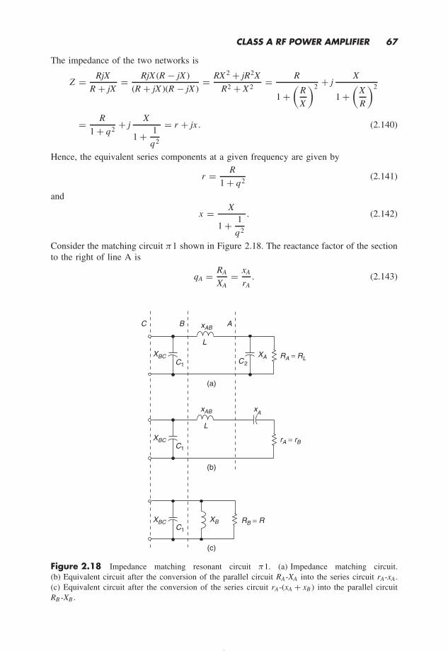
CLASS A RF POWER AMPLIFIER 67
The impedance of the two networks is
Z = RjX
R + jX= RjX (R − jX )
(R + jX )(R − jX )= RX 2 + jR2X
R2 + X 2= R
1 +(
R
X
)2 + jX
1 +(
X
R
)2
= R
1 + q2+ j
X
1 + 1
q2
= r + jx . (2.140)
Hence, the equivalent series components at a given frequency are given by
r = R
1 + q2(2.141)
and
x = X
1 + 1
q2
. (2.142)
Consider the matching circuit π1 shown in Figure 2.18. The reactance factor of the sectionto the right of line A is
qA = RA
XA= xA
rA. (2.143)
(a)
C1
RA = RLXBC
L
xAB
C2
XA
(b)
C1
rA = rBXBC
L
xAB xA
(c)
C1
RB = RXBC XB
C B A
Figure 2.18 Impedance matching resonant circuit π1. (a) Impedance matching circuit.(b) Equivalent circuit after the conversion of the parallel circuit RA-XA into the series circuit rA-xA.(c) Equivalent circuit after the conversion of the series circuit rA-(xA + xB ) into the parallel circuitRB -XB .

68 RF POWER AMPLIFIERS
The equivalent series resistance and reactance of the circuit to the right of line A are
rA = rB = RA
1 + q2A
= RL
1 + q2A
(2.144)
and
xA = XA
1 + 1q2
A
. (2.145)
The loaded quality factor is
QL = xAB
rA. (2.146)
The series reactance to the right of the B line is
xB = xAB − xA = (QL − qA)rA. (2.147)
The reactance factor of the circuit to the right of line B is
qB = xB
rB= R
XB= R
XCD(2.148)
resulting in
RB = R = rB (1 + q2B ) (2.149)
and
XB = xB
(1 + 1
q2B
). (2.150)
Example 2.2
Design an impedance matching circuit to meet the specifications: RL = 50 , R = 15.68 ,and f = 1 GHz.
Solution. Assume qB = 3. The reactance XCD is
XBC = 1
ω0C1= R
qB= 15.68
3= 5.227 (2.151)
producing
C1 = 1
ω0XBC= 1
2π × 109 × 5.227= 30.45 pF. (2.152)
Now
rB = rA = R
1 + q2B
= 15.68
32 + 1= 1.568 (2.153)
which gives
qA =√
RL
rA− 1 =
√50
1.568− 1 = 5.558. (2.154)
The reactance of C2 is
XA = 1
ω0C2= RL
qA= 50
5.558= 8.996 (2.155)

CLASS A RF POWER AMPLIFIER 69
resulting in
C2 = 1
ωXA= 1
2π × 109 × 8.996= 17.69 pF. (2.156)
The loaded quality factor is
QL = xAB
rA= xB
rB+ xA
rA= qB + qA = 3 + 5.558 = 8.558. (2.157)
Thus
xAB = ω0L = QLrA = 8.558 × 1.568 = 13.419 . (2.158)
and
L = xAB
ω0= 13.419
2π × 109= 2.136 nH. (2.159)
2.9 Class A RF Linear Amplifier
2.9.1 Amplifier of Variable-envelope Signals
Modern wireless communication systems use power amplifiers to amplify variable-envelopesignals. Linear amplifiers are required to amplify variable-envelope signals, such as AMsignals. The Class A amplifier is a linear amplifier. Figure 2.19 shows waveforms of gate-to-source voltage vGS and drain-to-source voltage vDS in an ideal linear power amplifier.
The modulating voltage at the amplifier input is given by
vim (t) = Vim cos ωmt . (2.160)
The carrier voltage at the amplifier input is
vic = Vic cos ωct . (2.161)
The gate-to-source AM voltage at the input of a Class A RF amplifier is
vGS = VGSQ + V (t) cos ωct = VGSQ + [Vic + vm (t)] cos ωct
= VGSQ + [Vc + Vim cos ωmt] cos ωc t = VGSQ + Vic (1 + m cos ωmt) cos ωct (2.162)
0
vDS
t0
vGS0
t
vGS
vDS
Q
Figure 2.19 Amplification of AM signal in Class A linear amplifier.

70 RF POWER AMPLIFIERS
where
m = Vim
Vic. (2.163)
To avoid distortion of the AM signal, the transistor must be ON at all times. The maximumamplitude of the ac component of the gate-to-source voltage occurs at m = 1:
Vgsm(max ) = Vic(1 + mmax ) = Vci (1 + 1) = 2Vic . (2.164)
The dc gate-to-source voltage at the operating point Q must satisfy the following condition:
VGSQ > 2Vic . (2.165)
Assuming a linear vDS = Av vGS relationship, we obtain the drain-to-source AM voltage
vDS = VDSQ + Av Vic (1 + m cos ωmt) cos ωct = VDSQ + Vc (1 + m cos ωmt) cos ωc t .(2.166)
where Av is the voltage gain of the amplifier and the amplitude of the carrer at the amplifieroutput is
Vc = Av Vic . (2.167)
To avoid distortion, the dc drain-to-source voltage at the operating point must satisfy thecondition:
VDSQ > 2Vc + VGSQ − Vt . (2.168)
The output AM voltage of the amplifier is
vo = Vc (1 + m cos ωmt) cos ωc t . (2.169)
2.9.2 Amplifiers of Constant-envelope Signals
The Class A amplifier can be used to amplify constant-envelope signals, such as angle-modulated signals (FM and PM signals). The gate-to-source FM voltage is
vgs = VDSQ + Vic cos(ωct + mf sin ωmt) (2.170)
where
VDSQ > Vic . (2.171)
Hence, the drain-to-source FM voltage is
vDS = VDSQ + Av Vc cos(ωc t + mf sin ωmt) = VDSQ + Vc cos(ωc t + mf sin ωmt) (2.172)
where
mf = f
fm(2.173)
Vc = Av Vic (2.174)
and
VDSQ > Vic + VGSQ − Vt . (2.175)

CLASS A RF POWER AMPLIFIER 71
2.10 Summary
• The conduction angle of the drain current is 2θ = 360 in the Class A power amplifier.
• The operating point of the transistor in the Class A amplifier is above the transistorthreshold voltage Vt such that the gate-to-source voltage waveform is above Vt for theentire voltage swing (Vgsm < VGS − Vt ). Therefore, the transistor never enters the cutoffregion.
• The transistor is biased at a current greater than the peak value of the ac component ofthe drain current (Im < ID ).
• There is no sharp dividing boundary between Class A power amplifiers and small-signalamplifiers.
• The dc supply power PI is constant in Class A RF power amplifier and is independentof the amplitude of the output voltage Vm .
• Power loss in the transistor of the Class A RF power amplifier is high.
• The Class A power amplifier dissipates the maximum power at zero output power.
• The maximum drain efficiency of Class A RF power amplifiers with the RF choke is50% at Im = II and Vm = VI .
• The harmonic distortion in Class A power amplifiers is low. Therefore, these circuits arelinear amplifiers, suitable for the amplification of AM signals.
• The Class A power amplifier suffers from low efficiency, but provides a higher linearitythan other power amplifiers.
• Negative feedback can be used to suppress the nonlinearity.
• The amplitude of the current in the parallel-resonant circuit is high.
• Power losses in the parallel-resonant circuit are high because the amplitude of the currentflowing through the resonant inductor and the resonant capacitor is QL times higher thanthat of the output current Im .
• The maximum drain efficiency of the Class A audio amplifier, in which the RF choke isreplaced by a resistor, is only 25% at Im = II and Vm = VI .
• The linearity of the Class A RF power amplifier is very good.
• The amplitudes of harmonics in the load current in the Class A amplifier are low.
• Class A power amplifiers are used as low-power drivers of high-power amplifiers and aslinear power amplifiers.
2.11 References
[1] L. Gray and R. Graham, Radio Transmitters, New York, NY: McGraw-Hill, 1961.[2] E. W. Pappenfus, Single Sideband Principles and Circuits, New York, NY: McGraw-Hill, 1964.

72 RF POWER AMPLIFIERS
[3] K. K. Clarke and D. T. Hess, Communications Circuits: Analysis and Design, Addison-WesleyPublishing Co., Reading, MA, 1971; reprinted Krieger, Malabar, FL, 1994.
[4] H. L. Krauss, C. W. Bostian, and F. H. Raab, Solid State Radio Engineering, New York, NY:John Wiley & Sons, 1980.
[5] M. K. Kazimierczuk and D. Czarkowski, Resonant Power Converters. New York: John Wiley& Sons, 1995.
[6] S. C. Cripps, RF Power Amplifiers for Wireless Communications, 2nd Ed., Artech House, Nor-wood: MA, 2006.
[7] M. Albulet, RF Power Amplifiers, Noble Publishing Co., Atlanta, GA, 2001.[8] T. H. Lee, The Design of CMOS Radio-Frequency Integrated Circuits, 2nd Ed. Cambridge
University Press, New York, NY, 2004.[9] B. Razavi, RF Microelectronics, Prentice-Hall, Upper Saddle River, NJ, 1998.
[10] A. Grebennikov, RF and Microwave Power Amplifier Design, McGraw-Hill, New York, NY,2005.
[11] A. Grebennikov and N. O. Sokal, Switchmode Power Amplifiers, Elsevier, Amsterdam, 2007.[12] J. Aguilera and R. Berenguer, Design and Test of Integrated Inductors for RF Applications,
Kluwer Academic Publishers, Boston, MA, 2003.[13] M. K. Kazimierczuk, Pulse-Width Modulated PWM DC-DC Power Converters, John Wiley &
Sons, New York, NY, 2008.
2.12 Review Questions
2.1 What is the value of the conduction angle of the drain current in the Class A poweramplifier?
2.2 What is the location of the transistor operating point for the Class A RF power ampli-fier?
2.3 Does the dc supply power depend on the output voltage amplitude Vm?
2.4 Is the power loss in the transistor of the Class A amplifier low?
2.5 Are the power losses in the parallel-resonant circuit high?
2.6 Is the efficiency of the Class A RF power amplifier high?
2.7 Is the linearity of the Class A RF power amplifier good?
2.8 Are the harmonics in the load current of the Class A RF power amplifier high?
2.9 What are the upper and lower limits of the output voltage in the Class A amplifier forlinear operation?
2.13 Problems
2.1 Determine the drain efficiency of a Class A amplifier with an RF choke to meet thefollowing specifications:
(a) VI = 20 V and Vm = 10 V.
(b) VI = 20 V and Vm = 18 V.

CLASS A RF POWER AMPLIFIER 73
2.2 Determine the maximum power loss in the transistor of the Class A amplifier with anRF choke, which has VI = 10 V and II = 1 A.
2.3 Design a Class A RF power amplifier to meet the following specifications: PO =0.25 W, VI = 1.5 V, VDS (min) = 0.2 V, and f = 2.4 GHz.
2.4 Design an impedance matching circuit for the RF Class A amplifier with RL = 50 ,R = 25 , and f = 2.4 GHz.


3Class AB, B, and C RFPower Amplifiers
3.1 Introduction
The Class B RF power amplifier [1–7] consists of a transistor and a parallel-resonant circuit.The transistor is operated as a dependent current source. The conduction angle of the drainor collector current in the Class B power amplifier is 180. The parallel resonant circuitacts like a bandpass filter and selects only the fundamental component. The efficiency ofthe Class B power amplifier is higher than that of the Class A power amplifier. The circuitof the Class C power amplifier is the same as that of the Class B amplifier. However, theoperating point is such that the conduction angle of the drain current is less than 180.Class B and C power amplifiers are usually used for RF amplification in radio and TVtransmitters as well as in mobile phones. In this chapter, we will present Class AB, B, andC RF power amplifiers with their principle of operation, analysis, and design examples.
3.2 Class B RF Power Amplifier
3.2.1 Circuit of Class B RF Power Amplifier
The circuit of a Class B RF power amplifier is shown in Figure 3.1. It consists of a transistor(MOSFET, MESFET, or BJT), parallel-resonant circuit, and RF choke. The operating pointof the transistor is located exactly at the boundary between the cutoff region and the activeregion (the saturation region or the pinch-off region). The dc component of the gate-to-source voltage VGS is equal to the transistor threshold voltage Vt . Therefore, the conductionangle of the drain current 2θ is 180. The transistor is operated as a voltage-controlleddependent-current source. Voltage and current waveforms in the Class B power amplifier
RF Power Amplifiers Marian K. Kazimierczuk 2008 John Wiley & Sons, Ltd

76 RF POWER AMPLIFIERS
(a)
VI
+voRCL
CC
Lf
II
io
+vDS
iD + VI
VGS
vgs+
−
−
−
−vGS
(b)
VI
+voRCL
CC
Lf
II
io
+vDS
iD
t
iD
0
+ VI
−
−
−
Figure 3.1 Class AB, B, or C RF power amplifiers.
are shown in Figure 3.2. The ac component of the gate-to-source voltage vgs is a sinewave. The drain current is a half sine wave and contains the dc component, fundamentalcomponent, and even harmonics. The parallel-resonant circuit acts as a bandpass filter,which attenuates all the harmonics. The ‘purity’ of the output sine wave is a function ofthe selectivity of the bandpass filter. The higher the loaded quality factor QL, the loweris the harmonic content of the sine wave output current and voltage. The parallel-resonantcircuit may be more complex to serve as an impedance matching network.
3.2.2 Waveforms of Class B Amplifier
The gate-to-source voltage is given by
vGS = Vt + Vgsm cos ωt . (3.1)
For large-signal operation, the drain current is nearly proportional to the gate-to-sourcevoltage vGS , when vGS is above Vt :
iD = K (vGS − Vt ) = KVgsm cos ωt for vGS > Vt (3.2)
and
iD = 0 for vGS < Vt . (3.3)

CLASS AB, B, AND C RF POWER AMPLIFIERS 77
ωt0
IDMiD
23π
2π
ωt0
vDS
VI
23π
2π
2π
ωt02
vGS
3π2π
2π
ωt023π
2π
2π
0
pD
2π
2π
23π ωt
Vt
vo
Vm
−
2π−
−
−
−
Figure 3.2 Waveforms in Class B RF power amplifier.
The drain current in the Class B amplifier is a half sine wave and is given by
iD =
IDM cos ωt for −π
2< ωt ≤ π
2
0 forπ
2< ωt ≤ 3π
2
(3.4)
where IDM is the peak value of the drain current. The drain-to-source voltage is expressed as
vDS = VI − Vm cos ωt . (3.5)

78 RF POWER AMPLIFIERS
The instantaneous power dissipation in the transistor is
pD (ωt) = iD vDS = IDM cos ωt(VI − Vm cos ωt) for − π
2< ωt ≤ π
2(3.6)
andpD (ωt) = 0 for
π
2< ωt ≤ 3π
2. (3.7)
The fundamental component of the drain current is
Im = 1
π
∫ π2
− π2
IDM cos2 ωt d(ωt) = IDM
2= π
2II . (3.8)
The drain current waveform is
iD = IDM cos ωt = π II cos ωt for − π
2< ωt ≤ π
2(3.9)
andiD = 0 for
π
2< ωt ≤ 3π
2. (3.10)
The drain-to-source voltage waveform is
vDS = VI − Vm cos ωt = VI
(1 − Vm
VI
)cos ωt . (3.11)
The instantaneous power dissipation in the transistor at f = f0 is
pD (ωt) = iD vDS = II VI π cos ωt
(1 − Vm
VIcos ωt
)
= PI π cos ωt
(1 − Vm
VIcos ωt
)for − π
2< ωt ≤ π
2(3.12)
andpD (ωt) = 0 for
π
2< ωt ≤ 3π
2. (3.13)
Hence, the normalized instantaneous power dissipation in the transistor is
pD (ωt)
PI= π cos ωt
(1 − Vm
VIcos ωt
)for − π
2< ωt ≤ π
2(3.14)
andpD (ωt)
PI= 0 for
π
2< ωt ≤ 3π
2. (3.15)
The normalized instantaneous power loss in the transistor at various values of Vm/VI and atf = f0 is shown in Figure 3.3 for the Class B power amplifier. As the ratio Vm/VI increases,the peak values of pD (ωt)/PI decrease, yielding higher drain efficiency.
3.2.3 Power Relationships in Class B Amplifier
The dc supply current is
II = 1
2π
∫ π2
− π2
iD d(ωt) = 1
2π
∫ π2
− π2
IDM cos ωt d(ωt) = IDM
π= 2
πIm = 2
π
Vm
R. (3.16)
Hence, the dc resistance seen by the dc power supply VI is
RDC = VI
II= π
2
VI
VmR. (3.17)

CLASS AB, B, AND C RF POWER AMPLIFIERS 79
−90 −75 −60 −45 −30 −15 0 15 30 45 60 75 900
0.2
0.4
0.6
0.8
1
1.2
1.4
1.6
1.8
wt (°)
pD (
ωt)
/PI
Vm/VI = 0.5
0.7
0.8
0.9
1
Figure 3.3 Normalized instantaneous power dissipation pD (ωt )/PI at various values of Vm/VI
and at f = f0 for the Class B RF power amplifier.
For Vm = VI ,
IImax = 2
π
VI
R(3.18)
resulting in the dc resistance seen by the power supply VI
RDCmin = VI
IImax= π
2R. (3.19)
The maximum value of RDC occurs at Vm = 0 and its value is RDCmax = ∞. The amplitudeof the output voltage is
Vm = RIm . (3.20)
The dc supply power is
PI = II VI = IDM
πVI = 2
πVI Im = 2
π
VI Vm
R= 2
π
(V 2
I
R
)(Vm
VI
). (3.21)
The output power is
PO = Im Vm
2= V 2
m
2R= 1
2
(V 2
I
R
)(Vm
VI
)2
. (3.22)
The power dissipation at the drain of the MOSFET is
PD = 1
2π
∫ π2
− π2
iD vDS d(ωt) = PI − PO = 2
π
VI Vm
R− V 2
m
2R
= 2
π
(V 2
I
R
)(Vm
VI
)− 1
2
(V 2
I
R
)(Vm
VI
)2
. (3.23)

80 RF POWER AMPLIFIERS
0 0.2 0.4 0.6 0.8 10
0.1
0.2
0.3
0.4
0.5
0.6
0.7
Vm /VI
PI /
(VI/R
), P
O /(
VI/R
), P
D /(
VI/R
)2
22
PI /(VI /R )2
PO /(VI /R )2
PD /(VI /R )2
Figure 3.4 Normalized dc supply power PI /(V 2I /R), normalized drain power PO/(V 2
I /R), andnormalized drain power dissipation PD/(V 2
I /R) as a function of Vm/VI for the Class B RF poweramplifier.
The maximum power dissipation can be determined by taking the derivative of PD withrespect to Vm and setting it to zero. Thus,
dPD
dVm= 2
π
VI
R− Vm
R= 0. (3.24)
The critical value of Vm at which the maximum power dissipation occurs is
Vm(cr) = 2VI
π. (3.25)
Hence, the maximum power dissipated in the drain of the transistor is
PDmax = 4
π2
V 2I
R− 2
π2
V 2I
R= 2
π2
V 2I
R. (3.26)
Figure 3.4 shows plots of PI /(V 2I /R), PO/(V 2
I /R), and PD/(V 2I /R) as a function of Vm/VI .
3.2.4 Efficiency of Class B Amplifier
The drain efficiency of the Class B RF power amplifier is
ηD = PO
PI= π
4
Vm
VI= π
4
(VI − VDSmin )
VI= π
4
(1 − VDSmin
VI
). (3.27)
For Vm = VI ,
ηD = POmax
PI= π
4≈ 78.54 %. (3.28)
The drain efficiency ηD as a function of Vm/VI is depicted in Figure 3.5.

CLASS AB, B, AND C RF POWER AMPLIFIERS 81
0 0.2 0.4 0.6 0.8 10
10
20
30
40
50
60
70
80
Vm /VI
η D (
%)
Figure 3.5 Drain efficiency ηD as a function of Vm/VI for the Class B RF power amplifier.
The maximum drain current is
IDM = π II = 2Im (3.29)
and the maximum drain-to-source voltage is
VDSM = 2VI . (3.30)
The output power capability is
cp = PO
VDSM IDM= ηD PI
VDSM IDM= ηD
II
IDM
VI
VDSM= π
4× 1
π× 1
2= 1
8= 0.125. (3.31)
It is interesting to note that the value of cp of the Class B amplifier is the same as that ofthe Class A amplifier.
Example 3.1
Design a Class B power amplifier to deliver power of 20 W at f = 2.4 GHz. The bandwidthis BW = 480 MHz. The power supply voltage is VI = 24 V and VDSmin = 2 V.
Solution. The maximum amplitude of the output voltage is
Vm = VI − VDSmin = 24 − 2 = 22 V. (3.32)
The load resistance is
R = V 2m
2PO= 222
2 × 20= 12.1 . (3.33)

82 RF POWER AMPLIFIERS
Pick R = 12 . The amplitude the fundamental component of the drain current and theoutput current is given by
Im = Vm
R= 22
12= 1.833 A. (3.34)
The dc supply current is
II = 2
πIm = 2
π× 1.833 = 1.167 A. (3.35)
The maximum drain current is
IDM = π II = π × 1.167 = 3.666 A (3.36)
and the maximum drain-to-source voltage is
VDSM = 2VI = 2 × 24 = 48 V. (3.37)
The dc supply power is
PI = II VI = 1.167 × 24 = 28 W. (3.38)
The drain power dissipation is
PD = PI − PO = 28 − 20 = 8 W. (3.39)
The drain efficiency is
ηD = PO
PI= 20
28= 71.43 %. (3.40)
The loaded quality factor is
QL = f
BW= 2.4
0.48= 5. (3.41)
The reactances of the resonant circuit components are
XL = XC = R
QL= 12
5= 2.4 (3.42)
yielding
L = XL
ω= 2.4
2π × 2.4 × 109= 0.1592 nH (3.43)
andC = 1
ωXC= 1
2π × 2.4 × 109 × 2.4= 27.6 pF. (3.44)
3.3 Class AB and C RF Power Amplifiers
3.3.1 Waveforms of Class AB and C RF Power Amplifiers
The circuit of the Class C power amplifier is the same as that of the Class B RF poweramplifier. The operating point of the transistor is located in the cutoff region. The dccomponent of the gate-to-source voltage VGS is less than the transistor threshold voltageVt . Therefore, the conduction angle of the drain current 2θ is less than 180. Voltageand current waveforms in the Class C power amplifier are shown in Figure 3.6. The onlydifference is the conduction angle of the drain current, which is determined by the operating

CLASS AB, B, AND C RF POWER AMPLIFIERS 83
ωt0
IDM
iD
23π
2π
ωt0
vDS
VI
23π
2π
2π
ωt02
vGS
3π2π
2π
ωt02
vo
3π2π
2π
0
pD
2π
2π
23π ωt
q
2π q
Vt
Vm
Figure 3.6 Waveforms in Class C RF power amplifier.
point. The drain current waveform for any conduction angle θ , i.e., for Class AB, Class B,and Class C, is given by
iD = IDM
cos ωt − cos θ
1 − cos θfor − θ < ωt ≤ θ
0 for θ < ωt ≤ 2π − θ.
(3.45)
84 RF POWER AMPLIFIERS
The drain current waveform is an even function of ωt and satisfies the condition: iD (ωt) =iD (−ωt). The drain current waveform can be expanded into Fourier series
iD (ωt) = IDM
[α0 +
∞∑n=1
αn cos nωt
]. (3.46)
The dc component of the drain current is
II = 1
2π
∫ θ
−θ
iD d(ωt) = 1
π
∫ θ
0iD d(ωt) = IDM
π
∫ θ
0
cos ωt − cos θ
1 − cos θd(ωt)
= IDMsin θ − θ cos θ
π (1 − cos θ )= α0IDM (3.47)
where
α0 = II
IDM= sin θ − θ cos θ
π (1 − cos θ ). (3.48)
The amplitude of the fundamental component of the drain current is given by
Im = 1
π
∫ θ
−θ
iD cos ωt d(ωt) = 2
π
∫ θ
0iD cos ωt d(ωt) = 2
π
∫ θ
0
cos ωt − cos θ
1 − cos θcos ωt d(ωt)
= IDMθ − sin θ cos θ
π (1 − cos θ )= α1IDM (3.49)
where
α1 = Im
IDM= θ − sin θ cos θ
π (1 − cos θ ). (3.50)
The amplitude of the n-th harmonic is
Im(n) = 1
π
∫ θ
−θ
iD cos nωt d(ωt) = 2
π
∫ θ
0iD cos nωt d(ωt)
= 2
π
∫ θ
0
cos ωt − cos θ
1 − cos θcos nωt d(ωt) = IDM
2
π
sin nθ cos θ − n cos nθ sin θ
n(n2 − 1)(1 − cos θ )= αn IDM
(3.51)where
αn = Im(n)
IDM= 2
π
sin nθ cos θ − n cos nθ sin θ
n(n2 − 1)(1 − cos θ )for n = 2, 3, 4, . . . . (3.52)
Figure 3.7 shows the Fourier coefficients αn as a function of the conduction angle θ .The ratio of the amplitude of the fundamental component to the dc component of the
drain current is given by
γ1 = Im
II= α1
α0= θ − sin θ cos θ
sin θ − θ cos θ. (3.53)
The ratio Im/II as a function of conduction angle θ of the drain current is shown inFigure 3.8.
The drain current waveform is given by
iD = IIπ (cos ωt − cos θ )
sin θ − θ cos θfor − θ ≤ ωt ≤ θ. (3.54)
The drain-to-source waveform at f = f0 is
vDS = VI − Vm cos ωt = VI
(1 − Vm
VI
)cos ωt . (3.55)

CLASS AB, B, AND C RF POWER AMPLIFIERS 85
0 20 40 60 80 100 120 140 160 180−0.1
0
0.1
0.2
0.3
0.4
0.5
0.6
q (°)
α n
α0
α1
α2
α3
α4α5
Figure 3.7 Fourier coefficients αn of the drain current iD as a function of the conduction angleθ for the Class AB, B, and C RF power amplifiers.
0 20 40 60 80 100 120 140 160 1801
1.1
1.2
1.3
1.4
1.5
1.6
1.7
1.8
1.9
2
q (°)
γ 1
Figure 3.8 Ratio of the fundamental component to the dc component Im/II of the drain currentiD as a function of conduction angle θ for the Class AB, B, and C RF power amplifiers.

86 RF POWER AMPLIFIERS
−120 −90 −60 −30 0 30 60 90 1200
0.25
0.5
0.75
1
1.25
1.5
wt (°)
pD (
wt)
/PI
Vm/VI = 0.5
0.7
0.8
0.9
1
Figure 3.9 Normalized drain power loss pD (ωt )/PI at conduction angle θ = 120 and at f = f0for the Class AB RF power amplifier.
The waveform of the normalized drain power loss at f = f0 is
pD (ωt)
PI= π (cos ωt − cos θ )
sin θ − θ cos θ
(1 − Vm
VIcos ωt
)for − θ ≤ ωt ≤ θ. (3.56)
The waveforms of the normalized drain power loss for θ = 120, 60 and θ = 45 at f = f0are shown in Figures 3.9, 3.10, and 3.11, respectively. As the conduction angle θ decreases,the peak values of pD (ωt)/PI increase.
The waveform of the normalized drain power loss at f not equal to f0 is
pD (ωt)
PI= π (cos ωt − cos θ )
sin θ − θ cos θ
[1 − Vm
VIcos(ωt + φ)
]for − θ ≤ ωt ≤ θ. (3.57)
The waveforms of the normalized drain power loss for θ = 60 at φ = 15 are shown inFigure 3.12.
3.3.2 Power of the Class AB, B, and C Amplifiers
The dc supply power is
PI = II VI = α0IDM VI . (3.58)
The output power is
PO = 1
2Im Vm = 1
2α1IDM Vm . (3.59)
The power dissipated in the transistor is
PD = PI − PO = α0IDM VI − 1
2α1IDM Vm . (3.60)

CLASS AB, B, AND C RF POWER AMPLIFIERS 87
−60 −45 −30 −15 0 15 30 45 600
0.5
1
1.5
2
2.5
wt (°)
pD (
wt)
/PI
Vm/VI = 0.5
0.7
0.8
0.9
1
Figure 3.10 Normalized drain power loss pD (ωt )/PI at conduction angle θ = 60 and at f = f0for the Class C RF power amplifier.
−45 −30 −15 0 15 30 450
0.5
1
1.5
2
2.5
3
3.5
wt (°)
pD (
wt)
/PI
Vm /VI = 0.5
0.7
0.8
0.9
1
Figure 3.11 Normalized drain power loss pD (ωt )/PI at conduction angle θ = 45 for the ClassC RF power amplifier.

88 RF POWER AMPLIFIERS
−60 −45 −30 −15 0 15 30 45 600
0.5
1
1.5
2
2.5
wt (°)
pD (
wt)
/PI
Vm /VI = 0.5
0.7
0.8
0.9
1
Figure 3.12 Normalized drain power loss pD (ωt )/PI at conduction angle θ = 60 and at φ = 15
for the Class C RF power amplifier.
The ratio of the fundamental component of the drain-to-source voltage Vm to the dc supplyvoltage VI is defined as
ξ1 = Vm
VI. (3.61)
3.3.3 Efficiency of the Class AB, B, and C Amplifiers
The efficiency of the Class AB, B, and C amplifiers is given by
ηD = PO
PI= 1
2
(Im
II
)(Vm
VI
)= 1
2γ1ξ1 = 1
2
α1
α0
Vm
VI= 1
2
(Vm
VI
)θ − sin θ cos θ
sin θ − θ cos θ
= θ − sin θ cos θ
2(sin θ − θ cos θ )
(1 − VDSmin
VI
). (3.62)
The drain efficiency ηD as a function of the conduction angle θ at selected values of Vm/VI
is illustrated in Figure 3.13. As the conduction angle θ decreases from 180 to 0, the drainefficiency ηD increases from 50 % to 100 % at Vm = VI .
The maximum drain-to-source voltage is
VDSM = VI + Vm = 2VI . (3.63)
The maximum drain current is
IDM = Im
α1. (3.64)

CLASS AB, B, AND C RF POWER AMPLIFIERS 89
0 20 40 60 80 100 120 140 160 1800
10
20
30
40
50
60
70
80
90
100
q (°)
η D (
%)
Vm /VI = 1
0.9
0.8
0.7
0.5
Figure 3.13 Drain efficiency ηD as a function of conduction angle θ at various values of Vm/VI
for the Class C RF power amplifier.
Thus, the maximum output power capability is
cp = PO
VDSM IDM=
12 Vm Im
2VI IDM= Im
4IDM= α1
4= θ − sin θ cos θ
4π (1 − cos θ ). (3.65)
The output power capability cp as a function of Vm/VI is shown in Figure 3.14. As theconduction angle θ approaches zero, cp also approaches zero.
3.3.4 Parameters of Class AB Amplifier at θ = 120
For 90 ≤ θ ≤ 180, we obtain the Class AB power amplifier. The Fourier coefficients ofthe drain current at the typical conduction angle θ = 120 are
α0 = II
IDM= 3
√3 + 2π
9π≈ 0.406 (3.66)
and
α1 = Im
IDM= 3
√3 + 8π
18π≈ 0.5363. (3.67)
The ratio of the fundamental component to the dc component of the drain current is given by
γ1 = Im
II= α1
α0= 3
√3 + 8π
2(3√
3 + 2π )= 1.321. (3.68)
The drain efficiency at θ = 120 is
ηD = PO
PI= 3
√3 + 8π
4(3√
3 + 2π )
(1 − VDSmin
VI
)≈ 0.6605
(1 − VDSmin
VI
). (3.69)

90 RF POWER AMPLIFIERS
0 20 40 60 80 100 120 140 160 1800
0.02
0.04
0.06
0.08
0.1
0.12
0.14
q (°)
c p
Figure 3.14 Output power capability cp as a function of conduction angle θ for the Class C RFpower amplifier.
The output power capability at θ = 120 is
cp = PO
VDSM IDM= 3
√3 + 8π
72π≈ 0.13408. (3.70)
Example 3.2
Design a Class AB power amplifier to deliver power of 12 W at f = 5 GHz. The bandwidthis BW = 500 MHz and the conduction angle is θ = 120. The power supply voltage isVI = 24 V and VDSmin = 1 V.
Solution. The maximum amplitude of the output voltage is
Vm = VI − VDSmin = 24 − 1 = 23 V. (3.71)
The load resistance is
R = V 2m
2PO= 232
2 × 12= 22 . (3.72)
The amplitude of the output current is
Im = Vm
R= 23
22= 1.04545 A. (3.73)
The dc supply current is
II = Im
γ1= 1.04545
1.321= 1.098 A. (3.74)

CLASS AB, B, AND C RF POWER AMPLIFIERS 91
For θ = 120, the maximum drain current is
IDM = II
α0= 1.4508
0.406= 3.573 A. (3.75)
The maximum drain-to-source voltage is
VDSM = 2VI = 2 × 24 = 48 V. (3.76)
The dc supply power is
PI = II VI = 1.098 × 24 = 26.352 W. (3.77)
The drain power dissipation is
PD = PI − PO = 26.352 − 12 = 16.9056 W. (3.78)
The drain efficiency is
ηD = PO
PI= 12
26.352= 45.52 %. (3.79)
The loaded quality factor is
QL = f
BW= 5
0.5= 10. (3.80)
The reactances of the resonant circuit components are
XL = XC = R
QL= 22
10= 2.2 (3.81)
yielding
L = XL
ω= 2.2
2π × 5 × 109= 0.07 nH (3.82)
and
C = 1
ωXC= 1
2π × 5 × 109 × 2.2= 14.47 pF. (3.83)
3.3.5 Parameters of Class C Amplifier at θ = 60
For θ < 90, we obtain the Class C amplifier. The Fourier coefficients of the drain currentat the typical conduction angle θ = 60 are
α0 = II
IDM=
√3
π− 1
3≈ 0.218 (3.84)
and
α1 = Im
IDM= 2
3−
√3
2π≈ 0.391. (3.85)
The ratio of the fundamental component to the dc component of the drain current is given by
γ1 = Im
II= α1
α0= 4π − 3
√3
2(3√
3 − π )= 1.7936. (3.86)
The drain efficiency at θ = 60 is
ηD = PO
PI= 4π − 3
√3
4(3√
3 − π )
(1 − VDSmin
VI
)≈ 0.8968
(1 − VDSmin
VI
). (3.87)

92 RF POWER AMPLIFIERS
The output power capability at θ = 60 is
cp = PO
VDSM IDM= 1
6−
√3
8π≈ 0.09777. (3.88)
Example 3.3
Design a Class C power amplifier to deliver power of 6 W at f = 2.4 GHz. The bandwidthis BW = 240 MHz and the conduction angle is θ = 60. The power supply voltage isVI = 12 V and VDSmin = 1 V.
Solution. The maximum amplitude of the output voltage is
Vm = VI − VDSmin = 12 − 1 = 11 V. (3.89)
The load resistance is
R = V 2m
2PO= 112
2 × 6= 10 . (3.90)
The amplitude of the output current is
Im = Vm
R= 11
10= 1.1 A. (3.91)
The dc supply current is
II = Im
γ1= 1.1
1.7936= 0.6133 A. (3.92)
For θ = 60, the maximum drain current is
IDM = II
α0= 0.6133
0.218= 2.813 A. (3.93)
The maximum drain-to-source voltage is
VDSM = 2VI = 2 × 12 = 24 V. (3.94)
The dc supply power is
PI = II VI = 0.6133 × 12 = 7.3596 W. (3.95)
The drain power dissipation is
PD = PI − PO = 7.3596 − 6 = 1.3596 W. (3.96)
The drain efficiency is
ηD = PO
PI= 6
7.3596= 81.52 %. (3.97)
The loaded quality factor is
QL = f
BW= 2.4
0.24= 10. (3.98)
The reactances of the resonant circuit components are
XL = XC = R
QL= 10
10= 1 (3.99)
yielding
L = XL
ω= 1
2π × 2.4 × 109= 0.0663 nH (3.100)

CLASS AB, B, AND C RF POWER AMPLIFIERS 93
and
C = 1
ωXC= 1
2π × 2.4 × 109 × 1= 66.63 pF. (3.101)
3.3.6 Parameters of Class C Amplifier at θ = 45
The Fourier coefficients of the drain current at the conduction angle θ = 45 are
α0 = II
IDM=
√2(4 − π )
4π (2 − √2)
≈ 0.16491 (3.102)
and
α1 = Im
IDM= π − 2
2π (2 − √2)
≈ 0.31016. (3.103)
The ratio Im/II is
γ1 = Im
II= α1
α0=
√2(π − 2)
4 − π= 1.8808. (3.104)
The drain efficiency at θ = 45 is
ηD = PO
PI= π − 2√
2(4 − π )
(1 − VDSmin
VI
)≈ 0.940378
(1 − VDSmin
VI
). (3.105)
The output power capability at θ = 60 is
cp = PO
VDSM IDM= π − 2
8π (2 − √2)
≈ 0.07754. (3.106)
Various coefficients for Class AB, B, and C power amplifiers are given in Table 3.1.
Table 3.1 Coefficients for Class AB, B, and C amplifiers.
θ α0 α1 γ1 ηD cp
10 0.0370 0.0738 1.9939 0.9967 0.0184520 0.0739 0.1461 1.9756 0.9879 0.0365130 0.1106 0.2152 1.9460 0.9730 0.0538140 0.1469 0.2799 1.9051 0.9526 0.0699845 0.1649 0.3102 1.8808 0.9404 0.077550 0.1828 0.3388 1.8540 0.9270 0.0847160 0.2180 0.3910 1.7936 0.8968 0.0977570 0.2525 0.4356 1.7253 0.8627 0.1088980 0.2860 0.4720 1.6505 0.8226 0.1180090 0.3183 0.5000 1.5708 0.7854 0.12500
100 0.3493 0.5197 1.4880 0.7440 0.12993110 0.3786 0.5316 1.4040 0.7020 0.13290120 0.4060 0.5363 1.3210 0.6605 0.13409130 0.4310 0.5350 1.2414 0.6207 0.13376140 0.4532 0.5292 1.1675 0.5838 0.13289150 0.4720 0.5204 1.1025 0.5512 0.1301160 0.4868 0.5110 1.0498 0.5249 0.12775170 0.4965 0.5033 1.0137 0.5069 0.12582180 0.5000 0.5000 1.0000 0.5000 0.12500

94 RF POWER AMPLIFIERS
Example 3.4
Design a Class C power amplifier to deliver power of 1 W at f = 2.4 GHz. The bandwidthis BW = 240 MHz and the conduction angle is θ = 45. The power supply voltage isVI = 5 V and VDSmin = 0.2 V.
Solution. The maximum amplitude of the output voltage is
Vm = VI − VDSmin = 5 − 0.2 = 4.8 V. (3.107)
The load resistance is
R = V 2m
2PO= 4.82
2 × 1= 11.52 . (3.108)
The amplitude of output current is
Im = Vm
R= 4.8
11.52= 0.416 A. (3.109)
The dc supply current is
II = Im
γ1= 0.416
1.808= 0.2211 A. (3.110)
For θ = 45, the maximum drain current is
IDM = II
α0= 0.2211
0.1613= 1.3707 A. (3.111)
The maximum drain-to-source voltage is
VDSM = 2VI = 2 × 5 = 10 V. (3.112)
The dc supply power is
PI = II VI = 0.2211 × 5 = 1.1055 W. (3.113)
The drain power dissipation is
PD = PI − PO = 1.1055 − 1 = 0.1055 W. (3.114)
The drain efficiency is
ηD = PO
PI= 1
1.1055= 90.45 %. (3.115)
The loaded quality factor is
QL = f
BW= 2.4
0.24= 10. (3.116)
The reactances of the resonant circuit components are
XL = XC = R
QL= 11.52
100= 1.152 (3.117)
yielding
L = XL
ω= 1.152
2π × 2.4 × 109= 0.07639 nH (3.118)

CLASS AB, B, AND C RF POWER AMPLIFIERS 95
andC = 1
ωXC= 1
2π × 2.4 × 109 × 1.152= 57.564 pF. (3.119)
3.4 Push-pull Complementary Class AB, B, and C RFPower Amplifiers
3.4.1 Circuit
A circuit of push-pull CMOS Class AB, B, or C RF power amplifiers is shown inFigure 3.15. It consists of complementary pair of transistors (NMOS and PMOS), a parallel-resonant circuit, and coupling capacitor CC . The transistors should have matched character-istics and are operated as voltage-dependent current sources. Since complementary transis-tors are used, the circuit is called a complementary push-pull amplifier or a complementary-symmetry push-pull amplifier. If MOSFETs are used, the circuit is called a CMOS push-pullpower amplifier. The circuit may also employ complementary bipolar junction transistors(CBJT): an npn transistor and a pnp transistor. A Class B push-pull amplifier uses one tran-sistor to amplify the positive portion of the input voltage and another transistor to amplifythe negative portion of the input voltage. The coupling capacitor CC blocks the dc voltagefrom the load. It also maintains the dc voltage VI /2 and supplies the PMOS transistor whenthe NMOS transistor is not conducting. Also, two supply voltages VI can be connected to
VI
R
iD1
vo
+vi
+ iD2
vDS2
+ Cc
Cc
iovDS1
+iD1 iD2
LC
(a)
(b)
VI
R vo
+vDS2
+
io
iD1
iD2
iD1
iD2
vDS1
+iD1 iD2
L C
t
t
Figure 3.15 Circuit of push-pull CMOS Class AB, B, and C RF power amplifiers.

96 RF POWER AMPLIFIERS
0
vi
ωtπ 2π
0Im
ωtπ 2π
io
0
Im
iD2
ωt
0
Im
iD1
ωt
π 2π
π 2π
0Vm
vo
ωtπ 2π
Figure 3.16 Current and voltage waveforms in push-pull CMOS Class B RF power amplifier.
the drains of both transistors. Current and voltage waveforms for the push-pull CMOSClass B RF power amplifier are shown in Figure 3.16. Similar waveforms can be drawnfor Class AB and C amplifiers.
3.4.2 Even Harmonic Cancellation in Push-pull Amplifiers
Let us assume that both transistors are identical. The drain current of the upper MOSFETcan be expanded into a Fourier series
iD1 = ID + id1 + id2 + id3 + · · · = ID + Idm1 cos ωt + Idm2 cos 2ωt + Idm3 cos 3ωt + · · ·(3.120)
The drain current of the lower MOSFET is shifted in phase with respect of the drain currentof the upper MOSFET by 180 and can be expanded into a Fourier series
iD2 = iD1(ωt − 180)
= ID + Idm1 cos(ωt − 180) + Idm2 cos 2(ωt − 180) + Idm3 cos 3(ωt − 180) + · · · .= ID − Idm1 cos ωt + Idm2 cos 2ωt − Idm3 cos 3ωt + · · · . (3.121)
Hence, the load current flowing through the coupling capacitor CB is
iL = iD1 − iD2 = 2Idm1 cos ωt + 3Idm3 cos 3ωt + · · · . (3.122)
Thus, cancellation of all even harmonics of the load current takes place in push-pull poweramplifiers, reducing distortion of the output voltage and the THD. Only odd harmonics

CLASS AB, B, AND C RF POWER AMPLIFIERS 97
must be filtered out by the parallel-resonant circuit, which is a bandpass filter. The sameproperty holds true for all push-pull amplifiers operating in all classes.
3.4.3 Power Relationships
Let us consider the Class B RF power amplifier. The output voltage is
vo = Vm cos ωt (3.123)
and the output current is
io = Im cos ωt (3.124)
and
Im = Vm
R= 2Idm (3.125)
where Idm = Idm1 is the peak value of the drain current. The ac output power is
PO = VmIm
2= V 2
m
2R= RI 2
m
2. (3.126)
The dc supply power is equal to the average value of the drain current of the upper transistor
II = 1
2π
∫ π/2
−π/2iD1 d(ωt) = Im
π= Vm
πR. (3.127)
The dc resistance is
RDC = VI
II= πVI
VmR. (3.128)
For Vm = 0, RDC = ∞. For Vm = VI , the dc resistance is
RDSmin = VI
IImax= πR. (3.129)
The dc supply power is
PI = VI II = VI Im
π= VI Vm
πR. (3.130)
The drain power dissipated in both transistors is
PD = PI − PO = VI Vm
πR− V 2
m
2R. (3.131)
Setting the derivative of PD to zero,
dPD
dVm= VI
πR− Vm
R= 0 (3.132)
we obtain
Vm(cr) = VI
π. (3.133)
Hence, the maximum power dissipation in both transistors is
PDmax = V 2I
2π2R. (3.134)

98 RF POWER AMPLIFIERS
The drain efficiency is
ηD = PO
PI= π
4
Vm
VI. (3.135)
For Vm = VI ,
ηDmax = π
4= 78.5 %. (3.136)
For Vm(max ) = VI − VDSmin ,
ηD = π
4
Vm(max )
VI= π
4
(1 − VDSmin
VI
). (3.137)
3.4.4 Device Stresses
The transistor current and voltage stresses are
IDM = Im (3.138)
and
VDSM = 2VI . (3.139)
The amplitudes of the currents through the resonant inductance and capacitance are
ILm = ICm = QLIm . (3.140)
The output-power capability is
cp = PO
2IDM VDSM= 1
4
(Im
IDM
)(Vm
VDSM
)= 1
4× 1 × 1
2= 1
8. (3.141)
Example 3.5
Design a CMOS Class B RF power amplifier to deliver power of 50 W at f = 1.8 GHz.The load resistance is RL = 50 . The bandwidth is BW = 180 MHz. The power supplyvoltage is VI = 48 V and VDSmin = 1 V.
Solution. Assuming the efficiency of the resonant circuit ηr = 0.95, the drain power is
PDS = PO
ηr= 50
0.95= 52.632 W. (3.142)
The amplitude of the drain-to-source voltage is
Vdm = VI − VDSmin = 48 − 1 = 47 V. (3.143)
The load resistance is
R = V 2dm
2PDS= 472
2 × 52.632= 20.985. (3.144)
The amplitude of the fundamental component of the drain current is
Idm = Vdm
R= 47
20.985= 2.2396 A (3.145)
II = 2
πIdm = 2
π× 2.2396 = 1.4257A. (3.146)

CLASS AB, B, AND C RF POWER AMPLIFIERS 99
The dc supply power is
PI = VI II = 48 × 1.4257 = 68.43 W. (3.147)
The total efficiency is
η = PO
PI= 50
68.43= 73.06 %. (3.148)
The maximum power loss in each transistor is
PDmax = V 2I
π2R= 482
π2 × 20.985= 11.124 W. (3.149)
The maximum drain current is
IDM = Idm = 2.2396 A. (3.150)
The maximum drain-to-source voltage is
VDSM = 2VI = 2 × 48 = 96 A. (3.151)
The loaded-quality factor is
QL = fcBW
= 1800
180= 10. (3.152)
The resonant inductance is
L = RL
ωQL= 20.985
2π × 1.8 × 109 × 10= 0.1855 nH. (3.153)
The resonant capacitance is
C = QL
ωRL= 10
2π × 1.8 × 109 × 20.985= 42.1 pF. (3.154)
3.5 Transformer-coupled Class B Push-pull Amplifier
3.5.1 Waveforms
A circuit of the transformer-coupled push-pull Class AB, B, and C RF power amplifiers isshown in Figure 3.17. Waveforms are depicted in Figure 3.18. The output current is
io = Im sin ωt = nIdm sin ωt (3.155)
where Im is the amplitude of the output current, Idm is the peak drain current and n is thetransformer turns ratio, equal to the ratio of number of turns of one primary to the numberof turns of the secondary
n = Im
Idm= Vdm
Vm. (3.156)
The output voltage is
vo = Vm sin ωt = Vdm
nsin ωt (3.157)
where the amplitude of the output current is
Vm = Im RL. (3.158)

100 RF POWER AMPLIFIERS
+vo
VI
LC
+
+vDS1
+vDS2
II
iD1
n :n :1
RL
iD2
i io
vi
+vGS1
+vGS2
+vp1
+vp2
+vs
Figure 3.17 Circuit of transformer-coupled push-pull Class AB, B, and C RF power amplifiers.
0
vi
wtπ 2π
wt
0
Im/niD1
wt
π 2π
π 2π
wt
0
nVmvDS1
0
vDS2
π 2π
0wtπ 2π
iD2
Imio
0wtπ 2π
Vm
vo
0ωtπ 2π
Im/n
nVm
Figure 3.18 Waveforms in transformer-coupled push-pull Class AB, B, and C RF poweramplifiers.

CLASS AB, B, AND C RF POWER AMPLIFIERS 101
The resistance seen by each transistor across each primary winding with the other primarywinding open is
R = n2RL. (3.159)
When the drive voltage is positive, transistor Q1 is ON and transistor Q2 is OFF. Thewaveforms are
iD1 = Idm sin ωt = Im
nsin ωt for 0 < ωt ≤ π (3.160)
iD2 = 0 (3.161)
vp1 = −iD1R = −iD1n2RL = vp2 = −RIdm sin ωt = − Im
nR sin ωt
= −nIm RL sin ωt (3.162)
and
vDS 1 = VI + vp1 = VI − iD1R = VI − iD1n2RL = VI − Idm R sin ωt
= VI − Im
nR sin ωt = VI − nIm RL sin ωt . (3.163)
When the drive voltage is negative, transistor Q1 is OFF and transistor Q2 is ON,
iD1 = 0 (3.164)
iD2 = −Idm sin ωt = − Im
nsin ωt for π < ωt ≤ 2π (3.165)
vp2 = iD2R = iD2n2RL = vp2 = −IdmR sin ωt = − Im
nR sin ωt
= −nImRL sin ωt (3.166)
and
vDS 2 = VI − vp2 = VI − iD2R = VI − iD2n2RL = VI + Idm R sin ωt = VI − Im
nRL sin ωt
= VI + nImRL sin ωt . (3.167)
The voltage between the drains of the MOSFETs is
vD1D2 = vp1 + vp2 = −n2RL(iD1 − iD2) = −2nRLIm sin ωt . (3.168)
Ideally, all even harmonics cancel out as shown in Section 3.4.1. The voltage across thesecondary winding is
vs = vD1D2
2n= −nRL
2(iD1 − iD2) = −RLIm sin ωt . (3.169)
The current through the dc voltage source VI is a full-wave rectified sinusoid given by
iI = iD1 + iD2 = Idm | sin ωt | = Im
n| sin ωt |. (3.170)
The dc supply current is
II = 1
2π
∫ 2π
0Idm | sin ωt | d(ωt) = 1
2π
∫ 2π
0
Im
n| sin ωt | d(ωt) = 2
π
Im
n= 2
π
Vm
nRL. (3.171)

102 RF POWER AMPLIFIERS
3.5.2 Power Relationships
The dc supply power is given by
PI = VI II = 2
π
VI Vm
nRL. (3.172)
The output power is
PO = V 2m
2RL. (3.173)
The drain power dissipation is
PD = PI − PO = 2
π
VI Vm
nRL− V 2
m
2RL. (3.174)
The derivative of the power PD with respect of the output voltage amplitude Vm is
dPD
dVm= 2
π
VI
nRL− Vm
RL= 0. (3.175)
resulting in the critical value of Vm at which the maximum value of the drain power lossPD occurs
Vm(cr) = 2
π
VI
n. (3.176)
The maximum drain power loss in both transistors is
PDmax = 2
π2
V 2I
n2RL= 2
π2
V 2I
R. (3.177)
The amplitude of the drain-to-source voltage is
Vdm = Vm
n= 2
πVI . (3.178)
The drain efficiency is
ηD = PO
PI= π
4
Vdm
VI= π
4
nVm
VI. (3.179)
For Vdm = nVm = VI , the dc supply power is
PI = VI II = 2
π
V 2I
n2RL= 2
π
V 2I
R. (3.180)
the output power is
PO = V 2m
2RL= n2V 2
I
2RL. (3.181)
and the drain efficiency isηDmax = π
4= 78.5 %. (3.182)
3.5.3 Device Stresses
The MOSFET current and voltage stresses are
IDM = Idm = Im
n(3.183)

CLASS AB, B, AND C RF POWER AMPLIFIERS 103
+
iD2 = ID − id1 + id2 − id3 + id4 ...
iD1 = ID + id1 + id2 + id3 + ...
Rvi
C
L
C
VI
RFC
II
id4+id2...+
id4+2(id2...+
++
+i d
32(
i d1
...i d
5 2ID)
)
Figure 3.19 A circuit of push-pull Class AB, B, and C RF power amplifiers with tappedcapacitor.
VI+
+vDS1
+vDS2
II
iD1
RL
iD2
vi
+vGS1
+vGS2
+vL1
+vL2
+voC
L2
L2
Figure 3.20 A circuit of push-pull Class AB, B, and C RF power amplifiers with tapped inductor.
andVDSM = 2VI . (3.184)
The output-power capability is
cp = POmax
2IDM VDSM= POmax
2IDM VDSM= 1
4
(Idm
ISM
)(Vm
VDSM
)= 1
4× 1 × 1
2= 1
8. (3.185)
A circuit of the push-pull Class AB, B, and C RF power amplifiers with tapped capacitoris depicted in Figure 3.19. This figure shows the distribution of the various componentsthrough the circuit and the cancellation of even harmonics in the load network. A circuitof the push-pull Class AB, B, and C RF power amplifiers with tapped inductor is shownin Figure 3.20. All equations for these two amplifiers can be obtained by setting n = 1 inthe equations for the push-pull amplifier shown in Figure 3.17.
Example 3.6
Design a transformer-coupled Class B power amplifier to deliver power of 25 W at f =2.4 GHz. The load resistance is RL = 50 . The bandwidth is BW = 240 MHz. The powersupply voltage is VI = 28 V and VDSmin = 1 V.

104 RF POWER AMPLIFIERS
Solution. Assuming the efficiency of the resonant circuit ηr = 0.94, the drain power is
PDS = PO
ηr= 25
0.94= 26.596 W. (3.186)
The resistance seen by each transistor across one part of the primary winding is
R = π2
2
V 2I
PDS= π2
2× 282
26.596= 145.469 . (3.187)
The transformer turns ratio is
n =√
R
RL=√
145.469
50= 1.7 ≈ 7
4. (3.188)
The maximum value of the drain-to-source voltage is
Vdm = πVI = π × 28 = 87.965 V. (3.189)
The amplitude of the drain current is
Idm = Vdm
R= 87.965
145.469= 0.605 A. (3.190)
The amplitude of the output voltage is
Vm = Vdm
n= 87.965
1.7= 51.74 V. (3.191)
The amplitude of the output current is
Im = Vm
RL= 51.74
50= 1.0348 A. (3.192)
The dc supply current is
II = π
2Idm = π
2× 0.605 = 0.95 A. (3.193)
The dc supply power is
PI = VI II = 28 × 0.95 = 26.6 W. (3.194)
The total efficiency is
η = PO
PI= 25
26.6= 93.98 %. (3.195)
The loaded-quality factor is
QL = fcBW
= 2.4
0.24= 10. (3.196)
The resonant inductance is
L = RL
ωQL= 50
2π × 2.4 × 109 × 10= 0.3316 nH. (3.197)
The resonant capacitance is
C = QL
ωRL= 10
2π × 2.4 × 109 × 50= 13.26 pF. (3.198)

CLASS AB, B, AND C RF POWER AMPLIFIERS 105
3.6 Class AB, B, and C Amplifiers ofVariable-envelope Signals
The Class AB, B, and C amplifier can be used to amplify variable-envelope signals, suchas AM signals. The ac component of the AM gate-to-source voltage is
vgs(AM ) = Vgsm (1 + min cos ωmt) cos ωct . (3.199)
(a)
(c)
(b)
wct
vDS
mout > min
vGS Vt
wct
vDS
mout = min
vGS Vt wct
wct
vDS
mout < min
vGS Vt wct
wct
Figure 3.21 Amplification of AM signals in Class AB, B, and C RF power amplifiers. (a) ClassAB amplifier (mout > min ). (b) Class B linear RF power amplifier (mout = min ). (c) Class C amplifier(mout < min ).

106 RF POWER AMPLIFIERS
+voRCL
CCio
+vDS
iD
VI
vm
+vGS
+
vm
+
vgs
VGS
RFC
CB
+
+
+ VI
Figure 3.22 Drain AM signals in Class AB, B, and C RF power amplifiers.
The overall AM gate-to-source voltage is
vGS = VGS + vgs(AM ) = VGS + Vgsm (1 + min cos ωm t) cos ωct . (3.200)
The AM drain current waveform of a power MOSFET is
iD = 1
2Cox Wvsat (vGS − Vt )
= 1
2Cox Wvsat [VGS − Vt + Vgsm (1 + min cos ωmt) cos ωct] for vGS > Vt . (3.201)
Assuming that the impedance of the parallel-resonant circuit Z is equal to R (i.e., Z ≈ R),we obtain the AM drain-to-source voltage
vDS ≈ RiD
= 1
2Cox Wvsat R[VGS − Vt + Vgsm (1 + min cos ωmt) cos ωct] for vGS > Vt . (3.202)
The choice of the class of operation, i.e., the operating point Q , has an important effecton nonlinear distortion of variable-envelope signals in RF power amplifiers in which tran-sistors are operated as voltage-dependent current sources. The amplification of AM signalsin Class AB, B, and C amplifiers is shown in Figure 3.21. Figure 3.21(a) illustrates theamplification of an AM signal in the Class AB amplifier, which produces an AM outputvoltage with mout > min . The output voltage exhibits shallower modulation than the inputsignal. Figure 3.21(b) illustrates the amplification of an AM signal in the Class B ampli-fier, where mout = min . The Class B amplifier behaves like a linear RF power amplifier.Its characteristic vDS = f (vGS − Vt ) is nearly linear and starts at the origin. Figure 3.21(c)illustrates the amplification of an AM signal in the Class C amplifier, which produces anAM output signal with mout < min . The output voltage exhibits deeper modulation than theinput signal. Class AB and C amplifiers can be used for amplifying AM signals with asmall modulation index m .
Figure 3.22 shows a circuit of Class AB, B, and C power amplifiers with AM modulation.In these amplifiers, an AM signal is generated by placing the modulating voltage sourcevm in series with the drain dc supply voltage source VI of a Class C RF power amplifierthat is driven into the ohmic (triode) region of the MOSFET. The gate-to-source voltagevGS has a constant amplitude Vgsm and its frequency is equal to the carrier frequency fc .The dc gate-to-source voltage VGS is fixed. Therefore, the conduction angle θ of the draincurrent iD is also fixed. These circuits require an audio-frequency transformer.
Class AB, B, and C power amplifiers can be used to amplify constant-envelope signals,such as FM and PM signals.

CLASS AB, B, AND C RF POWER AMPLIFIERS 107
3.7 Summary
• The Class B RF power amplifier consists of a transistor, parallel resonant circuit, RFchoke, and blocking capacitor.
• The transistor in the Class B power amplifier is operated as a dependent-current source.
• The conduction angle of the drain or collector current in the Class B power amplifier is180.
• The drain efficiency of the Class B power amplifier ηD is high. Ideally, ηD = 78.5 %.
• The conduction angle of the drain or collector current in the Class C power amplifier isless than 180.
• The transistor is operated as a dependent-current source in the Class C power amplifier.
• The drain efficiency of the Class AB and C power amplifiers ηD increases from 50 % to100 % as the conduction angle θ decreases from 180 to 0 at Vm = VI .
• The drain efficiency of the Class C power amplifier is 89.68 % at θ = 60 and Vm = VI .
• The drain efficiency of the Class C power amplifier is 94.04 % at θ = 45 and Vm = VI .
• Class B and C RF power amplifiers are narrowband circuits because the resonant circuitacts like a bandpass filter.
• Class B and C RF power amplifiers are linear (or semilinear) because the amplitude ofthe drain current is proportional to the amplitude of the gate-to-source voltage.
• Class B and C RF power amplifiers are used as medium and high-power narrowbandlinear power amplifiers.
• A push-pull Class B power amplifier uses one transistor to amplify the positive portionof the input voltage and another transistor to amplify the negative portion of the inputvoltage. One transistor is ‘pushing’ the current into the load and the other transistor is‘pulling’ the current from the load.
• In the push-pull topology, even harmonics are cancelled in the load, reducing distortionof the output voltage and the THD.
• The transformer in the transformer-coupled push-pull power amplifier performs theimpedance matching function.
3.8 References
[1] K. L. Krauss, C. V. Bostian, and F. H. Raab, Solid State Radio Engineering, New York, NY:John Wiley & Sons, 1980.
[2] M. Albulet, RF Power Amplifiers, Noble Publishing Co., Atralta, Ga, 2001.[3] S. C. Cripps, RF Power Amplifiers for Wireless Communications, Artech House, Norwood, MA,
1999.[4] M. K. Kazimierczuk and D. Czarkowski, Resonant Power Converters, John Wiley & Sons, 1995.[5] T. H. Lee, The Design of CMOS Radio-Frequency Integrated Circuits, 2nd Ed. Cambridge Uni-
versity Press, New York, NY, 2004.

108 RF POWER AMPLIFIERS
[6] A. Grebennikov, RF and Microwave Power Amplifier Design, McGraw-Hill, New York, NY,2005.
[7] H. L. Krauss and J. F. Stanford, ‘Collector modulation of transistor amplifiers,’ IEEE Transactionson Circuit Theory, vol. 12, pp. 426–428, September 1965.
3.9 Review Questions
3.1 List the components of the Class B RF power amplifier.
3.2 What is the transistor mode of operation in the Class B RF power amplifier?
3.3 What is the location of the operating point of the Class B RF power amplifier?
3.4 How high is the drain efficiency of the Class B RF power amplifier?
3.5 What is the mode of operation of the transistor in the Class C RF power amplifier?
3.6 What is the location of the operating point of the Class C RF power amplifier?
3.7 What is the drain efficiency of the Class C RF power amplifier at θ = 60 and θ =45?
3.8 Are the drain current and output voltage dependent on the gate-to-source voltage inClass B and C amplifiers?
3.9 Explain the principle of operation of the CMOS push-pull Class B RF power amplifier.
3.10 Explain the principle of operation of the transformer-coupled push-pull Class B RFpower amplifier.
3.11 What kind of harmonics is present in the load in push-pull amplifiers?
3.12 How does the transformer contribute to the impedance matching in power amplifiers?
3.10 Problems
3.1 Design a Class B RF power amplifier to meet the following specifications: VI = 3.3 V,PO = 1 W, VDSmin = 0.2 V, BW = 240 MHz, and f = 2.4 GHz.
3.2 Design a Class AB RF power amplifier to meet the following specifications: VI = 48 V,PO = 22 W, VDSmin = 1 V, θ = 120, BW = 90 MHz, and f = 0.9 GHz.
3.3 Design a Class C RF power amplifier to meet the following specifications: VI = 3.3 V,PO = 0.25 W, VDSmin = 0.2 V, θ = 60, BW = 240 MHz, and f = 2.4 GHz.
3.4 Design a Class C RF power amplifier to meet the following specifications: VI = 12 V,PO = 6 W, VDSmin = 1 V, θ = 45, BW = 240 MHz, and f = 2.4 GHz.

4Class D RF Power Amplifiers
4.1 Introduction
Class D RF resonant power amplifiers [1–18], also called Class D dc-ac resonant powerinverters, were was invented in 1959 by Baxandall [1] and have been widely used invarious applications [2–12] to convert dc energy into ac energy. Examples of applicationsof resonant amplifiers are radio transmitters, dc-dc resonant converters, solid-state electronicballasts for fluorescent lamps, high-frequency electric heating applied in induction welding,surface hardening, soldering and annealing, induction sealing for tamper-proof packaging,fiber-optics production, and dielectric heating for plastic welding. In Class D amplifiers,transistors are operated as switches. Class D amplifiers can be classified into two groups:
• Class D voltage-switching (or voltage-source) amplifiers;
• Class D current-switching (or current-source) amplifiers.
Class D voltage-switching amplifiers are fed by a dc voltage source. They employ (1)a series-resonant circuit or (2) a resonant circuit that is derived from the series-resonantcircuit. If the loaded quality factor is sufficiently high, the current through the resonantcircuit is sinusoidal and the current through the switches is a half sine wave. The voltagewaveforms across the switches are square waves.
In contrast, Class D current-switching amplifiers are fed by a dc current source in theform of an RF choke and a dc voltage source. These amplifiers contain a parallel-resonantcircuit or a resonant circuit that is derived from the parallel-resonant circuit. The voltageacross the resonant circuit is sinusoidal for high values of the loaded quality factor. Thevoltage across the switches is a half-wave sinusoid, and the current through the switches issquare wave.
One main advantage of Class D voltage-switching amplifiers is the low voltage acrosseach transistor, which is equal to the supply voltage. This makes these amplifiers suitablefor high-voltage applications. For example, a 220 V or 277 V rectified line voltage is usedto supply the Class D amplifiers. In addition, low-voltage MOSFETs can also be used. Such
RF Power Amplifiers Marian K. Kazimierczuk 2008 John Wiley & Sons, Ltd

110 RF POWER AMPLIFIERS
MOSFETs have a low on-resistance, reducing the conduction losses and operating junctiontemperature. This yields high efficiency. The MOSFET’s on-resistance rDS increases con-siderably with increasing junction temperature. This causes the conduction loss rDS I 2
rms toincrease, where Irms is the rms value of the drain current. Typically, rDS doubles as thetemperature rises by 100 C (for example, from 25 to 125 C), doubling the conduction loss.The MOSFET’s on-resistance rDS increases with temperature T because both the mobilityof electrons µn ≈ K1/T 2.5 and the mobility of holes µp ≈ K2/T 2.7 decrease with T for100 K≤ T ≤400 K, where K1 and K2 are constants. In many applications, the output poweror the output voltage can be controlled by varying the operating frequency f (FM control)or phase shift (phase control).
In this chapter, we study Class D half-bridge and full-bridge series-resonant amplifiers.The design procedure of the Class D amplifier is illustrated with detailed examples.
4.2 Circuit Description
Figure 4.1 shows the circuit of a Class D voltage-switching (voltage-source) RF poweramplifier with a pulse transformer driver. The circuit consists of two n-channel MOSFETs,a series resonant circuit, and a driver. It is difficult to drive the upper MOSFET. A high-side gate driver is required. A pulse transformer can be used to drive the MOSFETs. Thenoninverting output of the transformer drives the upper MOSFET and the inverting outputthe transformer drives the lower MOSFET. A pump-charge IC driver can also be used. Acircuit of the Class D voltage-switching RF power amplifier with two power supplies VI
and −VI is depicted in Figure 4.2 [14].Figure 4.3 shows a circuit of the Class D CMOS RF power amplifier, in which a PMOS
MOSFET QP and an NMOS MOSFET QN are used as switching devices. This circuitcan be integrated for high-frequency applications, such as RF transmitters for wirelesscommunications. The CMOS Class D amplifier requires only one driver. However, cross-conduction of both transistors during the MOSFETs transitions may cause spikes in thedrain currents. Nonoverlapping gate-to-source voltages may reduce this problem, but thedriver will become more complex [16, 17]. The peak-to-peak value of the gate-to-sourcedrive voltage vG is equal or close to the dc supply voltage VI , like in CMOS digital gates.Therefore, this circuit is appropriate only for low values of the dc supply voltage VI , usuallybelow 20 V. At high values of the dc supply voltage VI , the gate-to-source voltage shouldalso be high, which may cause voltage breakdown of the gate.
+R
VI
vO
L C
Figure 4.1 Class D half-bridge voltage-switching (voltage-source) RF power amplifier with aseries-resonant circuit and a pulse transformer driver.

CLASS D RF POWER AMPLIFIERS 111
+R
L C
VI
VI
+vi
vo
Figure 4.2 Class D half-bridge voltage-switching (voltage-source) RF power amplifier with aseries-resonant circuit and a pulse transformer driver.
L C
VI
QP
QN
vG vOR
++
Figure 4.3 Class D CMOS half-bridge voltage-switching (voltage-source) RF power amplifierwith a series-resonant circuit.
R
L C
+
vGvO
+QN
QP
VI
Cb
Figure 4.4 Class D half-bridge RF power amplifier with a voltage mirror driver [5].
Figure 4.4 shows the circuit of a Class D RF power amplifier with a voltage mirrordriver or voltage level shifter [5]. The dc supply voltage VI can be much higher than thepeak-to-peak voltage of the gate-to-source voltage. Therefore, this circuit can be used inhigh voltage applications.
A circuit of the Class D half-bridge RF power amplifier [1–12] with a series-resonant cir-cuit and a pulse transformer driver is shown in Figure 4.5(a). It consists of two bidirectional

112 RF POWER AMPLIFIERS
(c)
C
i
L
v R++
(d)
C
i
L
v R
r
++
(a)
+
+
Ci L
+R
(b)
C
i
L
+R
VI
VI
vR
vR
vR
vR
iS1
iS2
Q1 D1
Q2 D2
S2
S1
vGS2
vGS1vDS1
vDS2
rDS1
rDS2
rDS
rL
rL
Rt
rC
rC
Figure 4.5 Class D half-bridge RF power amplifier with a series-resonant circuit. (a) Circuit.(b)–(d) Equivalent circuits.
switches S1 and S2 and a series-resonant circuit L-C -R. Each switch consists of a transistorand an antiparallel diode. The MOSFET’s intrinsic body-drain pn junction diode may beused as an antiparallel diode in case of an inductive load, which will be discussed shortly.The switch can conduct either positive or negative current. However, it can only acceptvoltages higher than the negative value of a forward diode voltage −VDon ≈ −1 V. A pos-itive or negative switch current can flow through the transistor if the transistor is ON. If thetransistor is OFF, the switch can conduct only negative current that flows through the diode.

CLASS D RF POWER AMPLIFIERS 113
The transistors are driven by nonoverlapping rectangular-wave voltages vGS 1 and vGS 2 witha dead time at an operating frequency f = 1/T . Switches S1 and S2 are alternately ON andOFF with a duty cycle of 50 % or slightly less. The dead time is the time interval, whenboth the switching devices are OFF. Input resistance R is an ac load to which the ac poweris to be delivered. If the amplifier is part of a dc-dc resonant converter, R represents aninput resistance of the rectifier.
There has been increasing interest in designing RF power amplifiers in digital technologyin the age of a system-on-chip (SoC). There is a trend to integrate a complete transceivertogether with the digital baseband subsystem on a single chip. There are two main issuesin designing power amplifiers in submicron CMOS technology: oxide breakdown and hotcarrier effects. Both these problems became worse as the technology scales down. Theoxide breakdown is a catastrophic effect and sets a limit on the maximum signal swing onthe MOSFET drain. The hot carrier effect reduces the reliability. It increases the thresholdvoltage and consequently degrades the performance of the transistors. Switching-mode RFpower amplifiers offer high efficiency and can be used for constant-envelope modulatedsignals, such as Gaussian minimum shift keying (GMSK) used in Global Systems forMobile (GSM) Communications.
Integrated MOSFETs may be used at low output power levels and discrete power MOS-FETs at high output power levels. In integrated MOSFETs, the source and the drain areon the same side of the chip surface, causing horizontal current flow from drain to sourcewhen the device is ON. When the device is OFF, the depletion region of the reverse-biaseddrain-to-body pn junction diode spreads into the lightly doped short channel, resulting in alow punch-through breakdown voltage between the drain and the source. The breakdownvoltage is proportional to the channel length L, whereas the maximum drain current isinversely proportional to the channel length L. If an integrated MOSFET is designed tohave a high breakdown voltage, its channel length must be increased, which reduces thedevice aspect ratio W /L and the maximum drain current decreases.
In integrated MOSFETs, two contradictory requirements are imposed on the region betweenthe drain and the source: a short channel to achieve a high drain current when the device isON and a long channel to achieve a high breakdown voltage when the device is OFF.
The iD -vDS characteristics of a MOSFET in the ohmic region are given by
iD = µnCox
(W
L
)[(vGS − Vt )vDS − v 2
DS
2
]for vGS > Vt and vDS < vGS − Vt .
(4.1)The large-signal channel resistance of a MOSFET in the ohmic region is given by
rDS = vDS
iD= 1
µnCox
(W
L
)(vGS − Vt − vDS /2)
for vDS < vGS − Vt (4.2)
which simplifies to the form
rDS ≈ 1
µnCox
(W
L
)(vGS − Vt )
for vDS 2(vGS − Vt ). (4.3)
The drain-to-source resistance of discrete power MOSFETs consists of the channel resis-tance, accumulation region resistance, neck region resistance, and drift region resistance[18]. The drift resistance is dominant in high voltage MOSFETs.
Equivalent circuits of the Class D amplifier are shown in Figure 4.5(b)–(d). In Figure4.5(b), the MOSFETs are modeled by switches whose on-resistances are rDS 1 and rDS 2.Resistance rL is the equivalent series resistance (ESR) of the physical inductor L and

114 RF POWER AMPLIFIERS
0 0
0wt wt wt
π π π2π 2π 2π
0
0 0
0 0
0
00
0
00 0
0
i i i
f < fo f > fof = fo
0
(a) (b) (c)
0
0
0
VI VI
vGS1
vGS2
vDS1
vDS2
iS1 iS1
iS2 iS2iS2
iS1
Vm
Im
Im
Im Im Im
Im ImII II II
Im Im
Vm Vm
vi1 vi1 vi1
vDS2 vDS2
vDS1 vDS1
vGS2vGS2
vGS1vGS1
VI VI
y y
Figure 4.6 Waveforms in the Class D half-bridge voltage-switching RF power amplifier. (a) Forf < fo . (b) For f = fo . (c) For f > fo .
resistance rC is the equivalent series resistance of the physical capacitor C . In Figure 4.5(c),rDS ≈ (rDS 1 + rDS 2)/2 represents the average equivalent on-resistance of the MOSFETs. InFigure 4.5(d), the total parasitic resistance is represented by
r = rDS + rL + rC , (4.4)
which yields an overall resistance in the series-resonant circuit
Rt = R + r ≈ R + rDS + rL + rC . (4.5)
4.3 Principle of Operation
The principle of operation of the Class D amplifier is explained by the waveforms sketchedin Figure 4.6. The voltage at the input of the series-resonant circuit is a square wave ofmagnitude VI . If the loaded quality factor QL = √
L/C /R of the resonant circuit is highenough (for example, QL ≥ 2.5), the current i through this circuit is nearly a sine wave.Only at f = fo , the MOSFETs turn on and off at zero current, resulting in zero switchinglosses and an increase in efficiency. In this case, the antiparallel diode never conducts.

CLASS D RF POWER AMPLIFIERS 115
In many applications, the operating frequency f is not equal to the resonant frequencyfo = 1/(2π
√LC ) because the output power or the output voltage is often controlled by
varying the operating frequency f (FM control). Figure 4.6(a), (b), and (c) shows thewaveforms for f < fo , f = fo , and f > fo , respectively. The tolerance of the gate-to-sourcevoltage turn-on time is indicated by the shaded areas. Each transistor should be turned offfor f < fo or turned on for f > fo in the time interval during which the switch currentis negative. During this time interval, the switch current can flow through the antiparalleldiode. To prevent cross-conduction (also called shoot-through current), the waveforms ofthe drive voltages vGS 1 and vGS 2 should be non-overlapping and have a sufficient dead time(not shown in Figure 4.6). At turn-off, MOSFETs have a delay time and bipolar junctiontransistors (BJTs) have a storage time. If the dead time of the gate-to-source voltagesof the two transistors is too short, one transistor remains ON while the other turns off.Consequently, both the transistors are ON at the same time and the voltage power supplyVI is short-circuited by the transistor on-resistances rDS 1 and rDS 2. For this reason, cross-conduction current pulses of magnitude Ipk = VI /(rDS 1 + rDS 2) flow through the transistors.For example, if VI = 200 V and rDS 1 = rDS 2 = 0.5 , Ipk = 200 A. The excessive currentstress may cause immediate failure of the devices. The dead time should not be too long,which will be discussed in Sections 4.3.1 and 4.3.2. The maximum dead time increases asf /fo increases for f > fo or decreases for f < fo . This is because the time interval duringwhich the switch current is negative becomes longer. The shortest dead time must be atf = fo . There are commercial IC drivers available, which have an adjustable dead time, forexample, TI 2525.
4.3.1 Operation Below Resonance
For f < fo , the series-resonant circuit represents a capacitive load. This means that thecurrent through the resonant circuit i leads the fundamental component vi1 of the voltagevDS 2 by the phase angle |ψ |, where ψ < 0. Therefore, the switch current iS 1 is positiveafter the switch turns on at ωt = 0 and iS 1 is negative before the switch turns off at ωt = π .The conduction sequence of the semiconductor devices is Q1-D1-Q2-D2. Notice that thecurrent in the resonant circuit is diverted from the diode of one switch to the transistor ofthe other switch (Figure 4.5). This causes a lot of problems, which is explained shortly.Consider the time, when the switch S2 is turned on, as shown in Figure 4.5. Prior to thistransition, the current i flows through the antiparallel diode D1 of the switch S1. Whentransistor Q2 is turned on by the drive voltage vGS 2, vDS 2 is decreased, causing vDS 1 toincrease. Therefore, the diode D1 turns off and the current i is diverted from D1 to Q2.There are three undesired effects, when the MOSFET turns on:
(1) reverse recovery of the antiparallel diode of the opposite switch;
(2) discharging the transistor output capacitance;
(3) Miller’s effect.
The most severe drawback for operating below resonance is the diode reverse-recoverystress when the diode turns off. The MOSFET’s intrinsic body-drain diode is a minoritycarrier device. Each diode turns off at a very large dv/dt , resulting in a large di/dt .It generates a large reverse-recovery current spike (turned upside down). This spike flowsthrough the other transistor because it cannot flow through the resonant circuit. The resonant

116 RF POWER AMPLIFIERS
inductor L does not permit an abrupt current change. Consequently, the spikes occur inthe switch current waveform at both turn-on and turn-off transitions of the switch. Themagnitude of these spikes can be much (for example, 10 times) higher than the magnitudeof the steady-state switch current. High current spikes may destroy the transistors andalways cause a considerable increase in switching losses and noise. During a part of thereverse-recovery interval, the diode voltage increases from −1 V to VI and both the diodecurrent and voltage are simultaneously high, causing a high reverse-recovery power loss.
The turn-off failure of the power MOSFETs may be caused by the second breakdown ofthe parasitic bipolar transistor. This parasitic bipolar transistor is an integral part of a powerMOSFET structure. The body region serves as the base of the parasitic BJT, the source asthe BJT emitter, and drain as the BJT collector. If the body-drain diode is forward biasedjust prior to the sudden application of drain voltage, the turn-on process of the parasiticbipolar transistor may be initiated by the reverse-recovery current of the antiparallel diode.The second breakdown of the parasitic BJT may destroy the power MOSFET structure.The second breakdown voltage is usually one-half of the voltage at which the device failsif the diode is forward biased. This voltage is denoted as VDSS by manufacturers. For thereasons given above, operation at f < fo should be avoided if power MOSFETs are tobe used as switches. For example, the current spikes can be reduced by adding Schottkyantiparallel diodes. Silicon Schottky diodes have low breakdown voltages, typically below100 V. However, silicon-carbide Schottky diodes have high breakdown voltages. Since theforward voltage of the Schottky diode is lower than that of the pn junction body diode,most of the negative switch current flows through the Schottky diode, reducing the reverse-recovery current of the pn junction body diode. Another circuit arrangement is to connecta diode in series with the MOSFET and an ultrafast diode in parallel with the seriescombination of the MOSFET and diode. This arrangement does not allow the intrinsicdiode to conduct and to store the excess minority charge. However, the higher numberof components, the additional cost, and the voltage drop across the series diode (whichreduces the efficiency) are undesirable. Also, the peak voltages of the transistor and theseries diode may become much higher than VI . Transistors with a higher permissible voltageand a higher on-resistance should be used. High voltage MOSFETs have high on-resistance.However, high on-resistance increases conduction loss. This method may reduce, but cannoteliminate the spikes. Snubbers should be used to slow down the switching process, andreverse-recovery spikes can be reduced by connecting a small inductance in series witheach power MOSFET.
For f < fo , the turn-off switching loss is zero, but the turn-on switching loss is not zero.The transistors are turned on at a high voltage, equal to VI . When the transistor is turnedon, its output capacitance is discharged, causing switching loss. Suppose that the upperMOSFET is initially ON and the output capacitance Cout of the upper transistor is initiallydischarged. When the upper transistor is turned off, the energy drawn from the dc inputvoltage source VI to charge the output capacitance Cout from 0 to VI is given by
WI =∫ T
0VI iCout dt = VI
∫ T
0iCout dt = VI Q (4.6)
where iCout is the charging current of the output capacitance and Q is the charge transferredfrom the source VI to the capacitor. This charge equals the integral of the current iCout overthe charging time interval, which is usually much shorter than the time period T of theoperating frequency f . Equation (4.6) holds true for both linear and nonlinear capacitances.If the transistor output capacitance is assumed to be linear, Q = Cout VI and (4.6) becomes
WI = Cout V2
I . (4.7)
CLASS D RF POWER AMPLIFIERS 117
The energy stored in the linear output capacitance at the voltage VI is
WC = 1
2Cout V
2I . (4.8)
The charging current flows through a resistance that consists of the on-resistance of thebottom MOSFET and lead resistances. The energy dissipated in this resistance is
WR = WI − WC = 1
2Cout V
2I (4.9)
which is the same amount of energy as that stored in the capacitance. Note that charging alinear capacitance from a dc voltage source through a resistance requires twice the energystored in the capacitance. When the upper MOSFET is turned on, its output capacitanceis discharged through the on-resistance of the upper MOSFET, dissipating energy in thattransistor. Thus, the energy dissipated during charging and discharging of the transistoroutput capacitance is
Wsw = Cout V2
I . (4.10)
Accordingly, the turn-on switching loss per transistor is
Pton = WC
T= 1
2fCout V
2I . (4.11)
The total power loss associated with the charging and discharging of the transistor outputcapacitance of each MOSFET is
Psw = Wsw
T= fCout V
2I . (4.12)
The charging and discharging process of the output capacitance of the bottom transistoris similar. In reality, the drain-source pn step junction capacitance is nonlinear. An anal-ysis of turn-on switching loss with a nonlinear transistor output capacitance is given inSection 4.8.2.
Another effect that should be considered at turn-on of the MOSFET is Miller’s effect.Since the gate-source voltage increases and the drain-source voltage decreases during theturn-on transition, Miller’s effect is significant, by increasing the transistor input capaci-tance, the gate drive charge, and drive power requirements, reducing the turn-on switch-ing speed.
The advantage of operating below resonance is that the transistors are turned off at nearlyzero voltage, resulting in zero turn-off switching loss. For example, the drain-source voltagevDS 1 is held at nearly −1 V by the antiparallel diode D1 when iS 1 is negative. During thistime interval, transistor Q1 is turned off by drive voltage vGS 1. The drain-source voltagevDS 1 is almost zero and the drain current is low during the MOSFET turn-off, yieldingzero turn-off switching loss in the MOSFET. Since vDS 1 is constant, Miller’s effect isabsent during turn-off, the transistor input capacitance is not increased by Miller’s effect,the gate drive requirement is reduced, and the turn-off switching speed is enhanced. Insummary, for f < fo , there is a turn-on switching loss in the transistor and a turn-off(reverse-recovery) switching loss in the diode. The transistor turn-off and the diode turn-onare lossless.
As mentioned earlier, the drive voltages vGS 1 and vGS 2 are nonoverlapping and havea dead time. However, this dead time should not be made too long. If the transistor Q1
is turned off too early when the switch current iS 1 is positive, diode D1 cannot conductand diode D2 turns on, decreasing vDS 2 to −0.7 V and increasing vDS 1 to VI . When thecurrent through D2 reaches zero, diode D1 turns on, vDS 1 decreases to −0.7 V, and vDS 2
increases to VI . These two additional transitions of each MOSFET voltage would resultin switching losses. Note that only the turn-on transition of each switch is forced and is

118 RF POWER AMPLIFIERS
directly controlled by the driver, while the turn-off transition is caused by the turn-on ofthe opposite transistor (i.e., it is automatic).
In very high power applications, thyristors with antiparallel diodes can be used as switchesin Class D amplifiers with a series-resonant circuit topologies. The advantage of suchan arrangement is that, for operation below resonance, thyristors are turned off naturallywhen the switch current crosses zero. Thyristors, however, require more complicated andpowerful drive circuitry, and their operating frequency range is limited to 20 kHz. Suchlow frequencies make the size and weight of the resonant components large, increasing theconduction losses.
4.3.2 Operation Above Resonance
For f > fo , the series-resonant circuit represents an inductive load and the current i lagsbehind the voltage vi1 by the phase angle ψ , where ψ > 0. Hence, the switch current isnegative after turn-on (for part of the switch ‘on’ interval) and positive before turn-off. Theconduction sequence of the semiconductor devices is D1-Q1-D2-Q2. Consider the turn-offof switch S1. When transistor Q1 is turned off by the drive voltage vGS 1, vDS 1 increases,causing vDS 2 to decrease. As vDS 2 reaches −0.7 V, D2 turns on and the current i is divertedfrom transistor Q1 to diode D2. Thus, the turn-off switch transition is forced by the driver,while the turn-on transition is caused by the turn-off transition of the opposite transistor,not by the driver. Only the turn-off transition is directly controllable.
The transistors are turned on at zero voltage. In fact, there is a small negative voltageof the antiparallel diode, but this voltage is negligible in comparison to the input voltageVI . For example, transistor Q2 is turned on by v2 when iS 2 is negative. Voltage vDS 2
is maintained at nearly −1 V by the antiparallel diode D2 during the transistor turn-ontransition. Therefore, the turn-on switching loss is eliminated, Miller’s effect is absent,transistor input capacitance is not increased by Miller’s effect, the gate drive power is low,and the turn-on switching speed is high. The diodes turn on at a very low di/dt . The diodereverse-recovery current is a fraction of a sine wave and becomes a part of the switchcurrent when the switch current is positive. Therefore, the antiparallel diodes can be slow,and the MOSFET’s body-drain diodes are sufficiently fast as long as the reverse-recoverytime is less than one-half of the cycle. The diode voltage is kept at a low voltage of theorder of 1 V by the transistor in on-state during the reverse-recovery interval, reducingthe diode reverse-recovery power loss. The transistor can be turned on not only when theswitch current is negative but also when the switch current is positive and the diode is stillconducting because of the reverse recovery current. Therefore, the range of the on-dutycycle of the gate-source voltages and the dead time can be larger. If the dead time is toolong, the current will be diverted from the recovered diode D2 to diode D1 of the oppositetransistor until transistor Q2 is turned on, causing extra transitions of both switch voltages,current spikes, and switching losses.
For f > fo , the turn-on switching loss is zero, but there is a turn-off loss in the transistor.Both the switch voltage and current waveforms overlap during turn-off, causing a turn-off switching loss. Also, Miller’s effect is considerable, increasing the transistor inputcapacitance, the gate drive requirements, and reducing the turn-off speed. An approximateanalysis of the turn-off switching loss is given in Section 4.8.3. In summary, for f > fo ,there is a turn-off switching loss in the transistor, while the turn-on transitions of thetransistor and the diode are lossless. The turn-off switching loss can be eliminated byadding a shunt capacitor to one of the transistors and using a dead time in the drivevoltages.

CLASS D RF POWER AMPLIFIERS 119
4.4 Topologies of Class D Voltage-source RF PowerAmplifiers
Figure 4.7 shows a Class D voltage-switching amplifier with various resonant circuits.These resonant circuits are derived from a series-resonant circuit. In Figure 4.7(b), Cc is alarge coupling capacitor, which can also be connected in series with the resonant inductor.The resonant frequency (that is, the boundary between the capacitive and inductive load)for the circuits of Figure 4.7(b)–(g) depends on the load. The resonant circuit shown inFigure 4.7(b) is employed in a parallel resonant converter. The circuit of Figure 4.7(d)is used in a series-parallel resonant converter. The circuit of Figure 4.7(e) is used in a
(a)
(b)
(c)
(d)
(e)
(f)
(g)
VI
Cc
Q1
Q2
D1
D2
Figure 4.7 Class D voltage-switching amplifier with various resonant circuits.

120 RF POWER AMPLIFIERS
CLL resonant converter. Resonant circuits of Figure 4.7(a), (f), and (g) supply a sinusoidaloutput current. Therefore, they are compatible with current-driven rectifiers. The ampli-fiers of Figures 4.7(b)–(e) produce a sinusoidal voltage output and are compatible withvoltage-driven rectifiers. A high-frequency transformer can be inserted in places indicatedin Figure 4.7.
Half-bridge topologies of the Class D voltage-switching amplifier are depicted in Figure4.8. They are equivalent for ac components to the basic topology of Figure 4.5. Figure 4.8(a)shows a half-bridge amplifier with two dc voltage sources. The bottom voltage sourceVI /2 acts as a short circuit for the current through the resonant circuit, resulting in thecircuit of Figure 4.8(b). A drawback of this circuit is that the load current flows throughthe internal resistances of the dc voltage sources, reducing efficiency. In Figure 4.8(c),blocking capacitors CB/2 act as short circuits for the ac component. The dc voltage acrosseach of them is VI /2, but the ac power is dissipated in the ESRs of the capacitors. Anequivalent circuit for the amplifier of Figure 4.8(c) is shown in Figure 4.8(d). This is auseful circuit if the dc power supply contains a voltage doubler. The voltage stress acrossthe filter capacitors is lower than that in the basic circuit of Figure 4.5. In Figure 4.8(e),the resonant capacitor is split into two halves, which are connected in parallel for the ac
R
2C
C
2C
L RL
2
C2
VI
VI
(b)
VI
2
VI
2
VIVI
C
(c)
(e) (f)
VI
2
VI
2
L
(a)
VI
2
2L RC
VI
L C
CBVI
(d)
CB
2
CB
2
CB
2
CB
2L C R
R
RC
Figure 4.8 Half-bridge topologies of the Class D voltage-switching amplifier. (a) With two dcvoltage sources. (b) Equivalent circuit of amplifier of Figure 4.8(a). (c) With two filter capacitors.(d) Equivalent circuit of amplifier of Figure 4.8(c). (e) With a resonant capacitor split into two halfs.(f) Equivalent circuit of amplifier of Figure 4.8(e).

CLASS D RF POWER AMPLIFIERS 121
component. This is possible because the dc input voltage source VI acts as a short circuit forthe ac component of the upper capacitor. The disadvantage of all transformerless versionsof the half-bridge amplifier of Figure 4.8 is that the load resistance R is not grounded.
4.5 Analysis
4.5.1 Assumptions
The analysis of the Class D amplifier of Figure 4.5 is based on the equivalent circuit ofFigure 4.5(d) and the following assumptions:
(1) The transistor and the diode form a resistive switch whose on-resistance is linear, theparasitic capacitances of the switch are neglected, and the switching times are zero.
(2) The elements of the series-resonant circuit are passive, linear, time invariant, and donot have parasitic reactive components.
(3) The loaded quality factor QL of the series-resonant circuit is high enough so that thecurrent i through the resonant circuit is sinusoidal.
4.5.2 Series-resonant Circuit
The parameters of the series-resonant circuit are defined as follows:
• the resonant frequency
ωo = 1√LC
; (4.13)
• the characteristic impedance
Zo =√
L
C= ωoL = 1
ωoC; (4.14)
• the loaded quality factor
QL = ωoL
R + r= 1
ωoC (R + r)= Zo
R + r=
√L
CR + r
; (4.15)
• the unloaded quality factor
Qo = ωoL
r= 1
ωoCr= Zo
r(4.16)
wherer = rDS + rL + rC (4.17)
andRt = R + r . (4.18)
The series-resonant circuit acts like a second-order bandpass filter. The bandwidth of thiscircuit is
BW = foQL
. (4.19)

122 RF POWER AMPLIFIERS
The loaded quality factor is defined as
QL ≡ 2πTotal average magnetic and electric energy stored at resonant frequency fo
Energy dissipated and delivered to load at resonant frequency fo
= 2πPeak magnetic energy at fo
Energy lost in one cycle at fo= 2π
Peak electric energy at foEnergy lost in one cycle at fo
= 2πWs
ToPRt= 2π
foWs
PRt= ωoWs
PO + Pr= Q
PO + Pr(4.20)
where Ws is the total energy stored in the resonant circuit at the resonant frequency fo =1/To , and Q = ωoWs is the reactive power of inductor L or capacitor C at the resonantfrequency fo .
The current waveform through the inductor L is given by
iL(ωt) = Im sin(ωt − ψ) (4.21)
resulting in the instantaneous energy stored in the inductor
wL(ωt) = 1
2LI 2
m sin2(ωt − ψ). (4.22)
The voltage waveform across the capacitor C is given by
vC (ωt) = VCm cos(ωt − ψ) (4.23)
resulting in the instantaneous energy stored in the capacitor
wC (ωt) = 1
2CV 2
Cm cos2(ωt − ψ). (4.24)
The total energy stored in the resonant circuit at any frequency is given by
ws (ωt) = wL(ωt) + wC (ωt) = 1
2[LI 2
m sin2(ωt − ψ) + CV 2Cm cos2(ωt − ψ)]. (4.25)
Since VCm = XC Im = Im/(ωC ), the total energy stored in the resonant circuit at any fre-quency can be expressed as
ws (ωt) = 1
2LI 2
m [sin2(ωt − ψ) + 1
ω2LCcos2(ωt − ψ)]
= 1
2LI 2
m
sin2(ωt − ψ) + 1(
ω
ωo
)2 cos2(ωt − ψ)
. (4.26)
For ω = ωo , the total energy stored in the resonant circuit Ws is equal to the peak magneticenergy stored in the inductor L
ws (ωt) = 1
2LI 2
m [sin2(ωt − ψ) + cos2(ωt − ψ)] = 1
2LI 2
m = Ws = WLmax . (4.27)
Because Im = VCm/XC = ωCVCm , the total energy stored in the resonant circuit at anyfrequency becomes
ws (ωt) = 1
2CV 2
Cm [ω2LC sin2(ωt − ψ) + cos2(ωt − ψ)]
= 1
2CV 2
Cm
[(ω
ωo
)2
sin2(ωt − ψ) + cos2(ωt − ψ)
]. (4.28)

CLASS D RF POWER AMPLIFIERS 123
For ω = ωo , the total energy stored in the resonant circuit Ws is equal to the peak electricenergy stored in the capacitor C
ws (ωt) = 1
2CV 2
Cm [sin2(ωt − ψ) + cos2(ωt − ψ)] = Ws = WCmax . (4.29)
For steady-state operation at the resonant frequency fo , the total instantaneous energy storedin the resonant circuit is constant and equal to the maximum energy stored in the inductor
Ws = WLmax = 1
2LI 2
m (4.30)
or, using (4.13), in the capacitor
Ws = WCmax = 1
2CV 2
Cm = 1
2C
I 2m
(ωoC )2= 1
2
I 2m
(C ω2o)
= 1
2LI 2
m . (4.31)
Substitution of (4.30) and (4.31) into (4.20) produces
QL = ωoLI 2m
2PRt= ωoCV 2
Cm
2PRt. (4.32)
The reactive power of the inductor at fo is Q = (1/2)VLm Im = (1/2)ωoLI 2m and of the
capacitor is Q = (1/2)Im VCm = (1/2)ωoCV 2Cm . Thus, the quality factor can be defined as
the ratio of the reactive power of the inductor or the capacitor to the real power dissipatedin the form of heat in all resistances at the resonant frequency fo . The total power dissipatedin Rt = R + r is
PRt = 1
2Rt I
2m = 1
2(R + r)I 2
m . (4.33)
Substitution of (4.30) or (4.31), and (4.33) into (4.20) gives
QL = ωoL
R + r= 1
ωoC (R + r). (4.34)
The average magnetic energy stored in the resonant circuit is
WL(AV ) = 1
2π
∫ 2π
0wL d(ωot) = 1
2LI 2
m × 1
2π
∫ 2π
0sin2(ωot) d(ωt) = 1
4LI 2
m . (4.35)
Similarly, the average electric energy stored in the resonant circuit is
WC (AV ) = 1
2π
∫ 2π
0wC d(ωot) = 1
2CV 2
Cm × 1
2π
∫ 2π
0cos2(ωot) d(ωt) = 1
4CV 2
Cm . (4.36)
Hence, the total average energy stored in the resonant circuit is
Ws = WL(AV ) + WC (AV ) = 1
4LI 2
m + 1
4CV 2
Cm = 1
2LI 2
m = 1
2CV 2
Cm . (4.37)
This leads to the loaded quality factor.For R = 0,
Pr = 1
2rI 2
m (4.38)
and the unloaded quality factor is defined as
Qo ≡ ωoWs
Pr= ωoL
r= ωoL
rDS + rL + rC= 1
ωoCr= 1
ωoC (rDS + rL + rC ). (4.39)
Similarly, the quality factor of the inductor is
QLo ≡ ωoWs
PrL= ωoL
rL(4.40)

124 RF POWER AMPLIFIERS
and the capacitor is
QCo ≡ ωoWs
PrC= 1
ωoCrC. (4.41)
4.5.3 Input Impedance of Series-resonant Circuit
The input impedance of the series-resonant circuit is
Z = R + r + j
(ωL − 1
ωC
)= (R + r)
[1 + jQL
(ω
ωo− ωo
ω
)]
= Zo
[R + r
Zo+ j
(ω
ωo− ωo
ω
)]= |Z | ejψ = R + r + jX (4.42)
where
|Z | = (R + r)
√1 + Q2
L
(ω
ωo− ωo
ω
)2
= Zo
√((R + r)
Zo
)2
+(
ω
ωo− ωo
ω
)2
= Zo
√1
Q2L
+(
ω
ωo− ωo
ω
)2
(4.43)
ψ = arctan
[QL
(ω
ωo− ωo
ω
)](4.44)
Rt = R + r = |Z | cos ψ (4.45)
X = |Z | sin ψ. (4.46)
The reactance of the resonant circuit becomes zero at the resonant frequency fo . From(4.44),
cos ψ = 1√1 + Q2
L
(ω
ωo− ωo
ω
)2. (4.47)
Figure 4.9 shows a three-dimensional representation of |Z |/Zo as a function of the normal-ized frequency f /fo and the loaded quality factor QL. Plots of |Z |/Zo and ψ as a functionof f /fo at fixed values of QL are shown in Figures 4.10 and 4.11.
For f < fo , ψ is less than zero, which means that the resonant circuit represents acapacitive load to the switching part of the amplifier. For f > fo , ψ is greater than zero,which indicates that the resonant circuit represents an inductive load. The magnitude ofimpedance |Z | is usually normalized with respect to Rt , but it is not a good normalizationif R changes, and therefore Rt = R + r is variable at fixed resonant components L and C .
4.5.4 Currents, Voltages, and Powers
When S1 is ON and S2 is OFF, v = VI . When S1 is OFF and S2 is ON, v = 0. Referring toFigure 4.5(d), the input voltage of the series-resonant circuit is a square wave
v ≈ vDS 2 =
VI , for 0 < ωt ≤ π
0, for π < ωt ≤ 2π.(4.48)

CLASS D RF POWER AMPLIFIERS 125
0.5
1
1.5
0
5
100
0.5
1
1.5
2
f /fo
|Z|/
Zo
QL
Figure 4.9 Plots of |Z |/Zo as a function of f /fo and QL.
0.5 1 1.50
0.2
0.4
0.6
0.8
1
1.2
1.4
1.6
5
2
|Z|/
Zo
f /fo
QL = 10
Figure 4.10 Modulus of the normalized input impedance |Z |/Zo as a function of f /fo at constantvalues of QL.

126 RF POWER AMPLIFIERS
0.5 1 1.5−90
−60
−30
0
30
60
90
ψ(°
)5
2
QL = 10
f /fo
Figure 4.11 Phase of the input impedance ψ as a function of f /fo at constant values of QL.
This voltage can be expressed by Fourier series
v ≈ vDS 2 = VI
2+ 2VI
π
∞∑n=1
1 − (−1)n
2nsin(nωt) = VI
1
2+
∞∑k=1
sin[(2k − 1)ωt]
2k − 1
= VI
(1
2+ 2
πsin ωt + 2
3πsin 3ωt + 2
5πsin 5ωt + · · ·
). (4.49)
The fundamental component of voltage v is
vi1 = Vm sin ωt (4.50)
where its amplitude is given by
Vm = 2VI
π≈ 0.637VI . (4.51)
This leads to the rms value of voltage vi1
Vrms = Vm√2
=√
2VI
π≈ 0.45VI . (4.52)
The series-resonant circuit acts like a bandpass filter. For frequencies lower than the resonantfrequency fo , the series-resonant circuit represents a high capacitive impedance. On theother hand, for frequencies higher than the resonant frequency fo , the series-resonant circuitrepresents a high inductive impedance. If the operating frequency f is close to the resonantfrequency fo , the impedance of the resonant circuit is very high for higher harmonics, andtherefore the current through the resonant circuit is approximately sinusoidal and equal tothe fundamental component
i = Im sin(ωt − ψ) (4.53)

CLASS D RF POWER AMPLIFIERS 127
where from (4.46), (4.47), and (4.51)
Im = Vm
|Z | = 2VI
π |Z | = 2VI cos ψ
πRt= 2VI
πRt
√1 + Q2
L
(ω
ωo− ωo
ω
)2
= 2VI
πZo
√(Rt
Zo
)2
+(
ω
ωo− ωo
ω
)2. (4.54)
Figure 4.12 shows a three-dimensional representation of Im/(VI /Zo ) as a function of f /foand Rt/Zo . Plots of Im/(VI /Zo) as a function of f /fo at fixed values of QL are depicted inFigure 4.13. It can be seen that high values of Im/(VI /Zo ) occur at the resonant frequencyfo and at low total resistance Rt . At f = fo , the amplitude of the current through the resonantcircuit and the transistors becomes
Imr = 2VI
πRt. (4.55)
The output voltage is also sinusoidal
vo = iR = Vm sin(ωt − ψ). (4.56)
The input current of the amplifier iI equals the current through the switch S1 and isgiven by
iI = iS 1 =
Im sin(ωt − ψ), for 0 < ωt ≤ π
0, for π < ωt ≤ 2π.(4.57)
0.5
1
1.5
0
5
100
2
4
6
8
f/foQL
I m /(
VI /
Zo)
Figure 4.12 Normalized amplitude Im/(VI /Zo ) of the current through the resonant circuit as afunction of f /fo and QL.

128 RF POWER AMPLIFIERS
0.5 1 1.50
1
2
3
4
5
6
7
f/fo
I m/(
VI /
Zo)
QL = 10
5
2
Figure 4.13 Normalized amplitude Im/(VI /Zo ) of the current in the resonant circuit as a functionof f /fo at fixed values of QL.
Hence, from (4.43), (4.46), and (4.51), one obtains the dc component of the input current
II = 1
2π
∫ 2π
0iS 1 d(ωt) = Im
2π
∫ π
0sin(ωt − ψ) d(ωt) = Im cos ψ
π= Vm cos ψ
π |Z |
= 2VI cos2 ψ
π2Rt= 2VI Rt
π2|Z |2 = Im
π
√1 + Q2
L
(ω
ωo− ωo
ω
)2
= 2VI
π2Rt
[1 + Q2
L
(ω
ωo− ωo
ω
)2] . (4.58)
At f = fo ,
II = Im
π= 2VI
π2Rt≈ VI
5Rt. (4.59)
The dc input power can be expressed as
PI = II VI = 2V 2I cos2 ψ
π2Rt= 2V 2
I
π2Rt [1 + Q2L
(ω
ωo− ωo
ω
)2
]
= 2V 2I Rt
π2Z 2o
[(Rt
Zo
)2
+(
ω
ωo− ωo
ω
)2] . (4.60)

CLASS D RF POWER AMPLIFIERS 129
At f = fo ,
PI = 2V 2I
π2Rt≈ V 2
I
5Rt. (4.61)
Using (4.54), one arrives at the output power
PO = I 2m R
2= 2V 2
I R cos2 ψ
π2R2t
= 2V 2I R
π2R2t
[1 + Q2
L
(ω
ωo− ωo
ω
)2]
= 2V 2I R
π2Z 2o
[(Rt
Zo
)2
+(
ω
ωo− ωo
ω
)2] . (4.62)
At f = fo ,
PO = 2V 2I R
π2R2t
≈ 2V 2I
π2R. (4.63)
Figure 4.14 depicts PO/(V 2I Rt/Z 2
o ) as a function of f /fo and QL. The normalized out-put power PO/(V 2
I Rt/Z 2o ) is plotted as a function of f /fo at different values of QL in
Figure 4.15. The maximum output power occurs at the resonant frequency fo and at lowtotal resistance Rt .
4.5.5 Current and Voltage Stresses
The peak voltage across each switch is equal to the dc input voltage
VSM = VI . (4.64)
0.5
1
1.5
0
5
100
0.5
1
1.5
2
2.5
f/foQL
P O/(
VI2 R
t /Z
o2 )
Figure 4.14 Normalized output power PO/(V 2I Rt/Z 2
o ) as a function of f /fo and QL.

130 RF POWER AMPLIFIERS
0.5 1 1.50
0.5
1
1.5
2
2.5
f /fo
P O/(
VI2 R
t /Z
o2 )QL = 10
5
2
Figure 4.15 Normalized output power PO/(V 2I Rt/Z 2
o ) as a function of f /fo at fixed values of QL.
The maximum value of the switch peak currents and the maximum amplitude of the currentthrough the resonant circuit occurs at f = fo . Hence, from (4.54)
ISM = Imr = Vm
Rt= 2VI
πRt. (4.65)
The ratio of the input voltage of the resonant circuit to the voltage across the capacitor Cis the voltage transfer function of the second-order low-pass filter. The amplitude of thevoltage across the capacitor C is obtained from (4.54)
VCm = Im
ωC= 2VI
π
(ω
ωo
)√(Rt
Zo
)2
+(
ω
ωo− ωo
ω
)2. (4.66)
A three-dimensional representation of VCm/VI is shown in Figure 4.16. Figure 4.17 showsplots of VCm/VI as a function of f /fo at fixed values of QL.
The ratio of the input voltage of the resonant circuit to the voltage across the inductorL is the transfer function of the second-order high-pass filter. The amplitude of the voltageacross the inductor L is expressed as
VLm = ωLIm =2VI
(ω
ωo
)
π
√(Rt
Zo
)2
+(
ω
ωo− ωo
ω
)2. (4.67)
Figure 4.18 shows VLm/VI as a function of f /fo and QL. Plots of VLm/VI as a function off /fo at constant values of QL are displayed in Figure 4.19. At f = fo ,
VCm(max ) = VLm(max ) = ZoImr = QLVm = 2VI QL
π. (4.68)

CLASS D RF POWER AMPLIFIERS 131
0.5
1
1.5
0
5
100
2
4
6
8
f/foQL
VC
m /V
I
Figure 4.16 Normalized amplitude VCm/VI of the voltage across the resonant capacitor C as afunction of f /fo and QL.
0.5 1 1.50
1
2
3
4
5
6
7
f /fo
VC
m/V
I
QL = 10
5
2
Figure 4.17 Normalized amplitude VCm/VI of the voltage across the resonant capacitor C as afunction of f /fo at fixed values of QL.

132 RF POWER AMPLIFIERS
0.5
1
1.5
0
5
100
2
4
6
8
f /foQL
VLm
/VI
Figure 4.18 Normalized amplitude VLm/VI of the voltage across the resonant inductor L as afunction of f /fo and QL.
0.5 1 1.50
1
2
3
4
5
6
7
f /fo
VLm
/VI
QL = 10
5
2
Figure 4.19 Normalized amplitude VLm/VI of the voltage across the resonant inductor L as afunction of f /fo at fixed values of QL.

CLASS D RF POWER AMPLIFIERS 133
The maximum voltage stress of the resonant components occurs at the resonant frequencyf ≈ fo , at a maximum dc input voltage VI = VImax , and at a maximum loaded quality factorQL. Actually, the maximum value of VLm occurs slightly above fo and the maximum valueof VCm occurs slightly below fo . However, this effect is negligible for practical purposes.At the resonant frequency f = fo , the amplitudes of the voltages across the inductor andcapacitor are QL times higher than the amplitude Vm of the fundamental component of thevoltage at the input of the resonant circuit, which is equal to the amplitude of the outputvoltage Vom .
The output power capability is give by
cp = PO
2ISM VSM= 1
4
(Im
ISM
)(Vm
VSM
)= 1
4× 1 ×
(2
π
)= 1
2π= 0.159. (4.69)
4.5.6 Operation Under Short-circuit and Open-circuitConditions
The Class D amplifier with a series-resonant circuit can operate safely with an open circuitat the output. However, it is prone to catastrophic failure if the output is short-circuited atf close to fo . If R = 0, the amplitude of the current through the resonant circuit and theswitches is
Im = 2VI
πr
√1 +
(Zo
r
)2 (ω
ωo− ωo
ω
)2. (4.70)
The maximum value of Im occurs at f = fo and is given by
ISM = Imr = 2VI
πr(4.71)
and the amplitudes of the voltages across the resonant components L and C are
VCm = VLm = Imr
ωoC= ωoLImr = ZoImr = 2VI Zo
πr= 2VI Qo
π. (4.72)
For instance, if VI = 320 V and r = 2 , ISM = Imr = 102 A and VCm = VLm = 80 kV.Thus, the excessive current in the switches and the resonant circuit, as well as the excessivevoltages across L and C , can lead to catastrophic failure of the amplifier.
vORResonantNetwork
MVr
SwitchingNetwork
MVs
VI
+
−
Figure 4.20 Block diagram of a Class D amplifier.

134 RF POWER AMPLIFIERS
4.6 Voltage Transfer Function
The Class D amplifier can be functionally divided into two parts: the switching network andthe resonant network. A block diagram of the Class D amplifier is shown in Figure 4.20.The switching part is composed of a dc input voltage source VI and a set of switches.The switches are controlled to produce a square-wave voltage v . Since a resonant circuitforces a sinusoidal current, only the power of the fundamental component is transferredfrom the switching part to the resonant part. Therefore, it is sufficient to consider only thefundamental component of the voltage v given by (4.50). A voltage transfer function ofthe switching part can be defined as
MVs ≡ Vrms
VI(4.73)
where Vrms is the rms value of the fundamental component vi1 of the voltage v . The resonantnetwork of the amplifier converts the square-wave voltage v into a sinusoidal current orvoltage signal. Because the dc input source VI and switches S1 and S2 form a nearly ideal acvoltage source, many resonant circuits can be connected in parallel. If the resonant circuitis loaded by a resistance R, a voltage transfer function of the resonant part is
MVr ≡ VO(rms)
Vrms= |MVr | ejϕ (4.74)
where Vrms is the phasor of voltage vi1 and VO(rms) is the phasor of the sinusoidal outputvoltage vO across R. The modulus of MVr is
|MVr | = VO(rms)
Vrms(4.75)
where VO(rms) is the rms value of vO . A voltage transfer function of the entire amplifier isdefined as a product of (4.73) and (4.75)
MVI = MVs |MVr | = VO(rms)
VI. (4.76)
Let us consider the half-bridge circuit. Using (4.52), one arrives at the voltage transferfunction from the input of the amplifier to the input of the series-resonant circuit
MVs =√
2
π= 0.45. (4.77)
The ac-to-ac voltage transfer function of the series-resonant circuit is
MVr = VO(rms)
Vrms= R
R + r + j
(ωL − 1
ωC
) = ηIr
1 + jQL
(ω
ωo− ωo
ω
) = |MVr | ejϕ (4.78)
from which
|MVr | = VO(rms)
Vrms= ηIr√
1 + Q2L
(ω
ωo− ωo
ω
)2(4.79)
ϕ = − arctan
[QL
(ω
ωo− ωo
ω
)](4.80)
where ηIr = R/(R + r) = R/Rt is the efficiency of the amplifier, by taking into accountthe conduction losses only (see Section 4.8.1). Figure 4.21 illustrates (4.79) in a three-dimensional space. Figure 4.22 shows the voltage transfer function |MVr | as a function off /fo at fixed values of QL for ηIr = 0.95.

CLASS D RF POWER AMPLIFIERS 135
0.50.75
11.25
1.5
02
46
810
0
0.2
0.4
0.6
0.8
1
f /foQL
|MV
r|
Figure 4.21 Three-dimensional representation of |MVr | as a function of f /fo and QL forηIr = 0.95.
0.5 1 1.50
0.1
0.2
0.3
0.4
0.5
0.6
0.7
0.8
0.9
1
f/fo
|MV
r|
QL = 2
5
10
Figure 4.22 Transfer function |MVr | as a function of f /fo at fixed values of QL for ηIr = 0.95.

136 RF POWER AMPLIFIERS
Rearrangement of (4.79) yields
f
fo=√
1 − (|MVr |/ηIr )2 + 4Q2L (|MVr |/ηIr )2 −
√1 − (|MVr |/ηIr )2
2QL(|MVr |/ηIr )for
f
fo≤ 1 (4.81)
and
f
fo=√
1 − (|MVr |/ηIr )2 + 4Q2L (|MVr |/ηIr )2 +
√1 − (|MVr |/ηIr )2
2QL(|MVr |/ηIr )for
f
fo≥ 1. (4.82)
Comparison of (4.54) and (4.79) yields
Im = 2VI |MVr |πRtηIr
. (4.83)
At constant values of |MVr |, the amplitude of the current through the series-resonant circuitIm is inversely proportional to the resistance Rt .
Combining (4.77) and (4.79) gives the magnitude of the dc-to-ac voltage transfer functionfor the Class D series-resonant amplifier
|MVI | = VO(rms)
VI= VO(rms)
Vrms
Vrms
VI= MVs |MVr | =
√2ηIr
π
√1 + Q2
L
(ω
ωo− ωo
ω
)2. (4.84)
The maximum value of MVI occurs at f /fo = 1 and MVImax = √2ηIr/π = 0.45ηIr . Thus,
the values of MVI range from 0 to 0.45ηIr .
4.7 Bandwidth of Class D Amplifier
Equation (4.79) represents the magnitude of the voltage transfer function of a bandpassfilter. The 3-dB bandwidth satisfies the following condition:
1√1 + Q2
L
(f
fo− fo
f
)2= 1√
2. (4.85)
Hence,
Q2L
(f
fo− fo
f
)2
= 1 (4.86)
resulting in two second-order equations. The first equation is
QL
(f
fo− fo
f
)= 1 (4.87)
yielding the quadratic (f
fo
)2
− 1
QL
(f
fo
)− 1 = 0 (4.88)
whose positive solution gives the upper 3-dB frequency
fH = fo
[√1 + 1
4Q2L
+ 1
2QL
]≈ fo
(1 + 1
2QL
). (4.89)

CLASS D RF POWER AMPLIFIERS 137
Similarly, the second equation is
QL
(f
fo− fo
f
)= −1 (4.90)
yielding the quadratic (f
fo
)2
+ 1
QL
(f
fo
)− 1 = 0 (4.91)
whose positive solution gives the lower 3-dB frequency
fL = fo
[√1 + 1
4Q2L
− 1
2QL
]≈ fo
(1 − 1
2QL
). (4.92)
Thus, the 3-dB bandwidth is obtained as
BW = f = fH − fL = foQL
. (4.93)
As the loaded quality factor QL decreases, the bandwidth BW increases.
4.8 Efficiency of Half-bridge Class D Power Amplifier
4.8.1 Conduction Losses
The conduction loss for the power MOSFET is
PrDS = rDS I 2m
4, (4.94)
for the resonant inductor is
PrL = rLI 2m
2, (4.95)
and for the resonant capacitor is
PrC = rC I 2m
2. (4.96)
Hence, the conduction power loss in both the transistors and the resonant circuit is
Pr = 2PrDS + PrL + PrC = (rDS + rL + rC )I 2m
2= rI 2
m
2. (4.97)
The output power is
PO = I 2mR
2. (4.98)
Neglecting the switching losses and the gate-drive losses and using (4.60) and (4.62), oneobtains the efficiency of the amplifier determined by the conduction losses only
ηIr = PO
PI= PO
PO + Pr= R
R + r= 1
1 + rR
= 1 − r
R + r
= 1 −(
ωoL
R + r
)(r
ωoL
)= 1 − QL
Qo. (4.99)

138 RF POWER AMPLIFIERS
Note that in order to achieve a high efficiency, the ratio of the load resistance R to theparasitic resistance r must be high. The efficiency is high, when QL is low and Qo is high.For example, for QL = 5 and Qo = 200, the efficiency is ηIr = 1 − 5/200 = 0.975.
The turn-on loss for operation below resonance is given in the next section and theturn-off loss for operation above resonance is given in Section 4.8.3. Expressions for theefficiency for the two cases are given in those sections.
4.8.2 Turn-on Switching Loss
For operation below resonance, the turn-off switching loss is zero; however, there is a turn-on switching loss. This loss is associated with the charging and discharging of the outputcapacitances of the MOSFETs. The diode junction capacitance is
Cj (vD ) = Cj 0(1 − vD
VB
)m = Cj 0V mB
(VB − vD )m, for vD ≤ VB (4.100)
where Cj 0 is the junction capacitance at vD = 0 and m is the grading coefficient; m = 1/2for step junctions and m = 1/3 for graded junctions. The barrier potential is
VB = VT ln
(NAND
n2i
)(4.101)
where ni is the intrinsic carrier density (1.5 × 1010 cm−3 for silicon at 25 C), NA is theacceptor concentration, and ND is the donor concentration. The thermal voltage is
VT = kT
q= T
11 609(V) (4.102)
where k = 1.38 × 10⁻²³ J/K is Boltzmann’s constant, q = 1.602 × 10⁻¹⁹ C is the chargeper electron, and T is the absolute temperature in K. For p+n diodes, a typical value of theacceptor concentration is NA = 1016 cm−3, and a typical value of the donor concentrationis ND = 1014 cm−3, which gives VB = 0.57 V. The zero-voltage junction capacitance isgiven by
Cj 0 = A
√√√√√ εrεoq
2VB
(1
ND+ 1
NA
) ≈ A
√εrεoqND
2VB, for ND NA (4.103)
where A is the junction area in cm2, εr = 11.7 for silicon, and εo = 8.85 × 10⁻¹⁴ (F/cm).Hence, Cj 0/A = 3.1234 × 10⁻¹⁶√ND (F/cm2). For instance, if ND = 1014 cm−3, Cj 0/A ≈ 3nF/cm2. Typical values of Cj 0 are of the order of 1 nF for power diodes.
The MOSFET’s drain-source capacitance Cds is the capacitance of the body-drain pnstep junction diode. Setting vD = −vDS and m = 1/2, one obtains from (4.100)
Cds (vDS ) = Cj 0√1 + vDS
VB
= Cj 0
√VB
vDS + VB, for vDS ≥ −VB . (4.104)
Hence,
Cds1
Cds2=√
vDS 2 + VB
vDS 1 + VB≈√
vDS 2
vDS 1(4.105)

CLASS D RF POWER AMPLIFIERS 139
where Cds1 is the drain-source capacitance at vDS 1 and Cds2 is the drain-source capacitance atvDS 2. Manufacturers of power MOSFETs usually specify the capacitances Coss = Cgd + Cds
and Crss = Cgd at VDS = 25 V, VGS = 0 V, and f = 1 MHz. Thus, the drain-source capaci-tance at VDS = 25 V can be found as Cds(25V ) = Coss − Crss . The interterminal capacitancesof MOSFETs are essentially independent of frequency. From (4.105), the drain-sourcecapacitance at the dc voltage VI is
Cds(VI ) = Cds(25V )
√25 + VB
VI + VB≈ 5Cds(25V )√
VI(F). (4.106)
The drain-source capacitance at vDS = 0 is
Cj 0 = Cds(25V )
√25
VB+ 1 ≈ 6.7Cds(25V ) (4.107)
for VB = 0.57 V. Also,
Cds (vDS ) = Cds(VI )
√VI + VB
vDS + VB≈ Cds(VI )
√VI
vDS. (4.108)
Using (4.104) and dQj = Cds dvDS , the charge stored in the drain-source junction capaci-tance at vDS can be found as
Qj (vDS ) =∫ vDS
−VB
dQj =∫ vDS
−VB
Cds (vDS ) dvDS
= Cj 0
√VB
∫ vDS
−VB
dvDS√vDS + VB
= 2Cj 0
√VB (vDS + VB )
= 2Cj 0VB
√1 + vDS
VB= 2(vDS + VB )Cds (vDS ) ≈ 2vDS Cds (vDS ) (4.109)
which, by substituting (4.106) at vDS = VI , simplifies to
Qj (VI ) = 2VI Cds(VI ) = 10Cds(25V )
√VI (C). (4.110)
Hence, the energy transferred from the dc input source VI to the output capacitance of theupper MOSFET after the upper transistor is turned off is
WI =∫ VI
−VB
vi dt = VI
∫ VI
−VB
i dt = VI Qj (VI )
= 2V 2I Cds(VI ) = 10
√V 3
I Cds(25V )(W). (4.111)
Using dWj = (1/2)Qj dvDS and (4.109), the energy stored in the drain-source junctioncapacitance Cds at vDS is
Wj (vDS ) = 1
2
∫ vDS
−V0
Qj dvDS = Cj 0
√V B
∫ vDS
−V0
√vDS + VB dvDS
= 2
3Cj 0
√VB (vDS + VB )
32 = 2
3Cds (vDS )(vDS + VB )2 ≈ 2
3Cds (vDS )v 2
DS . (4.112)
Hence, from (4.106) the energy stored in the drain-source junction capacitance at vDS =VI is
Wj (VI ) = 2
3Cds(VI )V
2I = 10
3Cds(25V )
√V 3
I (J). (4.113)

140 RF POWER AMPLIFIERS
This energy is lost as heat when the transistor turns on and the capacitor is dischargedthrough rDS , resulting in the turn-on switching power loss per transistor
Ptron = Wj (VI )
T= fWj (VI ) = 2
3fCj 0
√VB (VI + VB )
32
= 2
3fCds(VI )V
2I = 10
3fCds(25V )
√V 3
I (W). (4.114)
Figure 4.23 shows Cds , Qj , and Wj as functions of vDS given by (4.104), (4.109), and(4.112).
Using (4.111) and (4.113), one arrives at the energy lost in the resistances of the chargingpath during the charging process of the capacitance Cds
Wchar (VI ) = WI (VI ) − Wj (VI ) = 4
3Cds(VI )V
2I = 20
3Cds(25V )
√V 3
I (J) (4.115)
Cds
Cj0
−VB 0
(a)
vDS
vDS−VB 0
Qj
(b)
vDS
Wj
−VB 0
(c)
Figure 4.23 Plots of Cds , Qj , and Wj versus vDS . (a) Cds versus vDS . (b) Qj versus vDS . (c) Wj
versus vDS .

CLASS D RF POWER AMPLIFIERS 141
and the corresponding power associated with the charging of the capacitance Cds is
Pchar = Wchar (VI )
T= fWchar (VI ) = 4
3fCds(VI )V
2I = 20
3fCds(25V )
√V 3
I (W). (4.116)
From (4.111), one arrives at the total switching power loss per transistor
Psw = W (VI )
T= fWI (VI ) = 2fCj 0VI
√VB (VI + VB )
= 2fCds(VI )V2
I = 10fCds(25V )
√V 3
I (W). (4.117)
The switching loss associated with charging and discharging an equivalent linear capacitanceCeq is Psw = fCeq V 2
I . Hence, from (4.117)
Ceq = 2Cds(VI ) = 10Cds(25V )√VI
. (4.118)
Example 4.1
For MTP5N40 MOSFETs, the data sheets give that Coss = 300 pF and Crss = 80 pF atVDS = 25 V and VGS = 0 V. These MOSFETs are to be used in a Class D half-bridgeseries-resonant amplifier that is operated at frequency f = 100 kHz and fed by dc voltagesource VI = 350 V. Calculate the drain-source capacitance at the dc supply voltage VI , thedrain-source capacitance at vDS = 0, the charge stored in the drain-source junction capac-itance at VI , the energy transferred from the dc input source VI to the output capacitanceof the MOSFET during turn-on transition, the energy stored in the drain-source junctioncapacitance Cds at VI , the turn-on switching power loss, and the total switching power lossper transistor in the amplifier operating below resonance. Assume VB = 0.57 V.
Solution. Using data sheets,
Cds(25V ) = Coss − Crss = 300 − 80 = 220 pF. (4.119)
From (4.106), one obtains the drain-source capacitance at the dc supply voltage VI = 350 V
Cds(VI ) = 5Cds(25V )√VI
= 5 × 220 × 10−12
√350
= 58.79 ≈ 59 pF. (4.120)
Equation (4.107) gives the drain-source capacitance at vDS = 0
Cj 0 = 6.7Cds(25V ) = 6.7 × 220 × 10−12 = 1474 pF. (4.121)
The charge stored in the drain-source junction capacitance at VI = 350 V is obtained from(4.110)
Qj (VI ) = 2VI Cds(VI ) = 2 × 350 × 59 × 10−12 = 41.3 nC. (4.122)The energy transferred from the input voltage source VI to the amplifier is calculated from(4.111) as
WI (VI ) = VI Qj (VI ) = 350 × 41.153 × 10−9 = 14.4 µJ (4.123)and the energy stored in the drain-source junction capacitance Cds at VI is calculated from(4.113) as
Wj (VI ) = 10
3Cds(25V )
√V 3
I = 10
3× 220 × 10−12
√3503 = 4.8 µJ. (4.124)

142 RF POWER AMPLIFIERS
Using (4.116), the power associated with charging the capacitance Cds is calculated as
Pchar = 20
3fCds(25V )
√V 3
I = 20
3× 105 × 220 × 10−12
√3503 = 0.96 W. (4.125)
From (4.114), the turn-on switching power loss per transistor for operating below reso-nance is
Ptron = 10
3fCds(25V )
√V 3
I = 10
3× 105 × 220 × 10−12
√3503 = 0.48 W. (4.126)
Using (4.117), one arrives at the total switching power loss per transistor for operatingbelow resonance
Psw = 10fCds(25V )
√V 3
I (W) = 10 × 105 × 220 × 10−12√
3503 = 1.44 W. (4.127)
Note that Ptron = 13 Psw and Pchar = 2
3 Psw . The equivalent linear capacitance is Ceq =2Cds(VI ) = 2 × 59 = 118 pF.
The overall power dissipation in the Class D amplifier is
PT = Pr + 2Psw + 2PG = rI 2m
2+ 20fCds(25V )
√V 3
I + 2fQg VGSpp . (4.128)
Hence, the efficiency of the half-bridge amplifier for operating below resonance is
ηI = PO
PO + PT= PO
PO + Pr + 2Psw + 2PG. (4.129)
4.8.3 Turn-off Switching Loss
For operation above resonance, the turn-on switching loss is zero, but there is a turn-offswitching loss. The switch current and voltage waveforms during turn-off for f > fo areshown in Figure 4.24. These waveforms were observed in various Class D experimentalcircuits. Notice that the voltage vDS 2 increases slowly at its lower values and much faster atits higher values. This is because the MOSFET output capacitance is highly nonlinear, andit is much higher at low voltage vDS 2 than at high voltage vDS 2. The current that chargesthis capacitance is approximately constant. The drain-to-source voltage vDS 2 during voltagerise time tr can be approximated by a parabolic function
vDS 2 = a(ωt)2. (4.130)
Because vDS 2(ωtr ) = VI , one obtains
a = VI
(ωtr )2. (4.131)
Hence, (4.130) becomes
vDS 2 = VI (ωt)2
(ωtr )2. (4.132)
The switch current during rise time tr is a small portion of a sinusoid and can be approxi-mated by a constant
iS 2 = IOFF. (4.133)

CLASS D RF POWER AMPLIFIERS 143
iS2vDS2
tftr ωt
ωt
IOFF
iS2
ωt
vDS2
vI
0
0
0
Figure 4.24 Waveforms of vDS 2, iD2, and iS 2vDS 2 during turn-off for f > fo .
The average value of the power loss associated with the voltage rise time tr is
Ptr = 1
2π
∫ 2π
0iS 2vDS 2 d(ωt) = VI IOFF
2π (ωtr )2
∫ ωtr
0(ωt)2 d(ωt)
= ωtr VI IOFF
6π= ftr VI IOFF
3= tr VI IOFF
3T. (4.134)
The switch current during fall time tf can be approximated by a ramp function
iS 2 = IOFF
(1 − ωt
ωtf
)(4.135)
and the drain-to-source voltage is
vDS 2 = VI (4.136)
which yields the average value of the power loss associated with the fall time tf of thecurrent of the semiconductor device
Ptf = 1
2π
∫ 2π
0iS 2vDS 2 d(ωt) = VI IOFF
2π
∫ ωtf
0
(1 − ωt
ωtf
)d(ωt)
= ωtf VI IOFF
4π= ftf VI IOFF
2= tf VI IOFF
2T. (4.137)

144 RF POWER AMPLIFIERS
Hence, the turn-off switching loss is
Ptoff = Ptr + Ptf = fVI IOFF
(tr3
+ tf2
). (4.138)
Usually tr is much longer than tf . The overall power dissipation in the Class D half-bridgeamplifier is
PT = Pr + 2Ptoff + 2PG = rI 2m
2+ fVI IOFF
(2tr3
+ tf
)+ 2fQg VGSpp . (4.139)
Hence, the efficiency of the amplifier for operation above resonance is
ηI = PO
PO + PT= PO
PO + Pr + 2Ptoff + 2PG. (4.140)
4.9 Design Example
A design procedure of the Class D voltage-switching power amplifier with a series-resonantcircuit is illustrated by means of an example.
Example 4.2
Design a Class D half-bridge amplifier of Figure 4.5 that meets the following specifi-cations: VI = 100 V, PO = 50 W, and f = 110 kHz. Assume QL = 5.5, ψ = 30 (that is,cos2ψ = 0.75), and the efficiency ηIr = 90 %. The converter employs IRF621 MOSFETs(International Rectifier) with rDS = 0.5 , Cds(25V ) = 110 pF, and Qg = 11 nC. Check theinitial assumption about ηIr using QLo = 300 and QCo = 1200. Estimate switching lossesand gate-drive power loss assuming VGSpp = 15 V.
Solution. From (4.99), the dc input power of the amplifier is
PI = PO
ηIr= 50
0.9= 55.56 W. (4.141)
Using (4.60), the overall resistance of the amplifier can be calculated as
Rt = 2V 2I
π2PIcos2 ψ = 2 × 1002
π2 × 55.56× 0.75 = 27.35 . (4.142)
Relationships (4.99) and (4.18) give the load resistance
R = ηIr Rt = 0.9 × 27.35 = 24.62 (4.143)
and the maximum total parasitic resistance of the amplifier
r = Rt − R = 27.35 − 24.62 = 2.73 . (4.144)
The dc supply current is obtained from (4.60)
II = PI
VI= 55.56
100= 0.556 A. (4.145)
The peak value of the switch current is
Im =√
2PO
R=√
2 × 50
24.62= 2.02 A (4.146)

CLASS D RF POWER AMPLIFIERS 145
and from (4.64) the peak value of the switch voltage is equal to the input voltage
VSM = VI = 100 V. (4.147)
Using (4.44), one arrives at the ratio f /fo at full load
f
fo= 1
2
(tan ψ
QL+√
tan2 ψ
Q2L
+ 4
)= 1
2
tan(30)
5.5+√
tan2(30)
5.52+ 4
= 1.054 (4.148)
from which
fo = f
(f /fo)= 110 × 103
1.054= 104.4 kHz. (4.149)
The values of the reactive components of the resonant circuit are calculated from (4.15) as
L = QLRt
ωo= 5.5 × 27.35
2π × 104.4 × 103= 229.3 µH (4.150)
C = 1
ωoQLRt= 1
2π × 104.4 × 103 × 5.5 × 27.35= 10 nF. (4.151)
From (4.14),
Zo =√
L
C=√
229.3 × 10⁻⁶
10 × 10−9= 151.427 . (4.152)
The maximum voltage stresses for the resonant components can be approximated using(4.68)
VCm(max ) = VLm(max ) = 2VI QL
π= 2 × 100 × 5.5
π= 350 V. (4.153)
Once the values of the resonant components are known, the parasitic resistance of theamplifier can be recalculated. From (4.40) and (4.41),
rL = ωL
QLo= 2π × 110 × 103 × 229.3 × 10−6
300= 0.53 (4.154)
and
rC = 1
ωCQCo= 1
2π × 110 × 103 × 10 × 10−9 × 1200= 0.12 . (4.155)
Thus, the parasitic resistance is
r = rDS + rL + rC = 0.5 + 0.53 + 0.12 = 1.15 . (4.156)
From (4.94), the conduction loss in each MOSFET is
PrDS = rDS I 2m
4= 0.5 × 2.022
4= 0.51 W. (4.157)
Using (4.95), the conduction loss in the resonant inductor L is
PrL = rLI 2m
2= 0.53 × 2.022
2= 1.08 W. (4.158)
From (4.96), the conduction loss in the resonant capacitor C is
PrC = rC I 2m
2= 0.12 × 2.022
2= 0.245 W. (4.159)
Hence, one obtains the overall conduction loss
Pr = 2PrDS + PrL + PrC = 2 × 0.51 + 1.08 + 0.245 = 2.345 W. (4.160)

146 RF POWER AMPLIFIERS
The efficiency ηIr associated with the conduction losses only at full power is
ηIr = PO
PO + Pr= 50
50 + 2.345= 95.52 %. (4.161)
Assuming the peak-to-peak gate-source voltage VGSpp = 15 V, the gate-drive power loss inboth MOSFETs is
2PG = 2fQg VGSpp = 2 × 110 × 103 × 11 × 10−9 × 15 = 0.036 W. (4.162)
The sum of the conduction losses and the gate-drive power loss is
PLS = Pr + 2PG = 2.245 + 0.036 = 2.38 W. (4.163)
The turn-on conduction loss is zero because the amplifier is operated above resonance. Theefficiency of the amplifier associated with the conduction loss and the gate-drive power atfull power is
ηI = PO
PO + PLS= 50
50 + 2.34= 95.45 %. (4.164)
4.10 Class D RF Power Amplifier with AmplitudeModulation
A circuit of the Class D power amplifier with amplitude modulation is shown in Figure 4.25.The modulating voltage source vm is connected in series with the dc supply voltage VI .Amplitude modulation can be accomplished in the Class D amplifier because the amplitudeof the output voltage is directly proportional to the dc supply voltage VI . Voltage waveformsthat explain the AM modulation process are depicted in Figure 4.26. The modulating voltagewaveform is given by
vm = Vm sin ωm t . (4.165)
The AM voltage waveform across the bottom switch is
v = vDS 2 = (VI + Vm sin ωmt)
1
2+ 2
π
∞∑k=1
sin[(2k − 1)ωc t]
2k − 1
. (4.166)
+voR
VI
L C
vI(t )
~+vm
+vm
Figure 4.25 Class D RF power amplifier with amplitude modulation.

CLASS D RF POWER AMPLIFIERS 147
v
0t
vm
t0
t0
t0
vDS2
vo
Figure 4.26 Waveforms in Class D RF power amplifier with amplitude modulation.
Sincesin x sin y = 1
2[cos(x − y) − cos(x + y)] (4.167)
we obtain the AM output voltage
vo = (VI + Vm sin ωc t)
(2
πsin ωct
)= 2
πVI
(1 + Vm
VIsin ωct
)sin ωc t
= Vc (1 + m sin ωc t) sin ωct = Vc sin ωct + mVc
2cos(ωc − ωm )t − mVc
2cos(ωc + ωm )t
(4.168)where the amplitude of the carrier is
Vc = 2
πVI . (4.169)
4.11 Transformer-coupled Push-pull Class DVoltage-switching RF Power Amplifier
4.11.1 Waveforms
A push-pull Class D voltage-switching (voltage-source) RF power amplifier is shown inFigure 4.27. Transistors are switched on and off alternately. Current and voltage waveforms

148 RF POWER AMPLIFIERS
+vo
VIL C
+vi
+vGS1
+vGS2
+vDS1
+vDS2
II +vs
+vp1
+vp2
iD1
n:n:1
RL
io
iD2
Figure 4.27 Push-pull Class D voltage-switching (voltage-source) RF power amplifier.
0
vGS1
ωt2ππvGS2
0ωt2ππ
vDS1
0ωt2ππ
2VI
vDS2
0ωt2ππ
2VI
0
iD1
ωt2ππ
0
iD2
ωt2ππ
0
io
ωt2ππ
Im
Im
0
vo
ωt
Vm
Vm2ππ
Im/n
Im/n
Figure 4.28 Waveforms in push-pull Class D voltage-switching (voltage-source) RF poweramplifier.
are depicted in Figure 4.28. The drain-to-source voltages vDS 1 and vDS 2 are square wavesand the drain currents iD1 and iD2 are half-sine waves.
For the operating frequency equal to the resonant frequency, the series-resonant circuitforces a sinusoidal output current
io = Im sin ωt (4.170)
CLASS D RF POWER AMPLIFIERS 149
resulting in a sinusoidal output voltage
vo = Vm sin ωt (4.171)
where
Vm = RLIm . (4.172)
The resistance seen by each transistor across each primary winding with the other primarywinding open is given by
R = n2RL (4.173)
where n is the transformer turn ratio of one primary winding to the secondary winding.For 0 < ωt ≤ π , the drive voltage is positive and the transistor Q1 is ON and the transistor
Q2 is OFF. The current and voltage waveforms are
vp2 = VI = vp1 (4.174)
vDS 1 = VI + vp1 = VI + VI = 2VI (4.175)
vs = vp1
n= vp2
n= VI
n(4.176)
and
iD1 = Idm sin ωt = Im
nsin ωt for 0 < ωt ≤ π (4.177)
and
iD2 = 0 (4.178)
where Idm is the peak drain current.For π < ωt ≤ 2π , the drive voltage is negative and transistor Q1 is OFF and transistor
Q2 is ON. The waveforms for this time interval are
vp1 = −VI = vp1 (4.179)
vDS 2 = VI − vp2 = VI − (−VI ) = 2VI (4.180)
vs = vp1
n= vp2
n= −VI
n(4.181)
iD1 = 0 (4.182)
and
iD2 = −Idm sin ωt = − Im
nsin ωt for π < ωt ≤ 2π. (4.183)
The amplitude of the fundamental component of the drain-to-source voltage is
Vdm = 4
πVI . (4.184)
The amplitude of the output voltage is
Vm = Vdm
n= 4
π
VI
n. (4.185)
The current through the dc voltage source VI is a full-wave rectified sinusoid
iI = iD1 + iD2 = Idm | sin ωt | = Im
n| sin ωt |. (4.186)

150 RF POWER AMPLIFIERS
The dc supply current is
II = 1
2π
∫ 2π
0
Im
n| sin ωt | d(ωt) = 2
π
Im
n= 2
πIdm = 2
π
Vm
n2RL= 8
π2
VI
n2RL. (4.187)
The dc resistance presented by the amplifier to the dc supply source VI is
RDC = VI
II= π2
8n2RL = VI
II= π2
8R. (4.188)
4.11.2 Power
The output power is
PO = V 2m
2RL= 8
π2
V 2I
n2RL= 8
π2
V 2I
R. (4.189)
The dc supply power is
PI = VI II = 8
π2
V 2I
n2RL. (4.190)
Neglecting conduction losses in the MOSFET on-resistances and switching losses, the drainefficiency is
ηD = PO
PI= 1. (4.191)
4.11.3 Current and Voltage Stresses
The MOSFET current and voltage stresses are
ISM = Im
n(4.192)
and
VSM = 2VI = πn
2Vm . (4.193)
The output-power capability is
cp = POmax
2IDM VDSM= 1
4
(IM
IDM
)(Vm
VDSM
)= 1
4× n × 2
2π= 1
2π= 0.159. (4.194)
4.11.4 Efficiency
The rms value of the drain current is
ISrms =√
1
2π
∫ 2π
π
I 2m
n2d(ωt) = Im
n√
2= Idm√
2. (4.195)
Hence, the conduction power loss in the MOSFET on-resistance rDS is
PrDS = rDS I 2Srms = rDS I 2
dm
2= rDS I 2
m
2n2= rDS
4n2RLPO . (4.196)

CLASS D RF POWER AMPLIFIERS 151
The drain efficiency is
ηD = PO
PO + 2PrDS= 1
1 + 2PrDS
PO
= 1
1 + rDS
n2RL
. (4.197)
The power loss in the ESR of the resonant inductor rL is
PrL = rLI 2m Q2
L
2= rLQ2
L
RLPO (4.198)
and the power loss in the ESR of the resonant capacitor rC is
PrC = rC I 2m Q2
L
2= rC Q2
L
RLPO . (4.199)
The total power loss is
PLoss = 2PrDS + PrL + PrC = PO
[rDS
n2RL+ Q2
L (rL + rC )
RL
]. (4.200)
Hence, the overall efficiency is
η = PO
PI= PO
PO + PLoss= 1
1 + rDS
n2RL+ Q2
L (rL + rC )
RL
. (4.201)
Example 4.3
Design a push-pull Class D voltage-switching RF power amplifier to meet the follow-ing specifications: VI = 28 V, PO = 50 W, RL = 50 , BW = 240 MHz, and f = 2.4 GHz.Neglect switching losses.
Solution. Assuming the efficiency of the resonant circuits ηr = 0.96, the drain power is
PDS = PO
ηr= 50
0.96= 52.083 W. (4.202)
Assume the minimum value of the drain-to-source voltage VDSmin = 1 V. The resistanceseen across one part of the primary winding is
R = 8
π2
(VI − VDSmin )2
PDS= 8
π2
(28 − 1)2
52.083= 11.345 W. (4.203)
The transformer turns ratio is
n =√
R
RL=√
11.345
50= 0.476. (4.204)
Pick n = 12 .
The amplitude of the fundamental component of the drain-to-source voltage is
Vdm = 4
πVI = 4
π× 28 = 35.65 V. (4.205)
The amplitude of the fundamental component of the drain current is
Idm = Vdm
R= 35.65
11.345= 3.142 A. (4.206)

152 RF POWER AMPLIFIERS
The dc supply voltage is
II = 2
πIdm = 2
π× 3.142 = 2 V. (4.207)
The dc supply power is
PI = VI II = 28 × 2 = 56 W. (4.208)
The rms value of each MOSFET is
ISrms = Idm√2
= 3.142√2
= 2.222 A. (4.209)
Assuming rDS = 0.2 , we obtain the conduction loss in each MOSFET
PrDS = rDS I 2Srms = 0.2 × 2.2222 = 0.9875 W. (4.210)
The drain efficiency is
ηD = PO
PO + 2PrDS= 50
50 + 2 × 0.9875= 96.2 %. (4.211)
The maximum drain current is
ISM = Idm = 3.142 A. (4.212)
The maximum drain-to-source voltage is
VSM = 2VI = 2 × 28 = 56 V. (4.213)
The loaded-quality factor is
QL = fcBW
= 2400
240= 10. (4.214)
The resonant inductance is
L = QLRL
ωc= 10 × 11.345
2π × 2.4 × 109= 7.523 nH. (4.215)
The resonant capacitance is
C = 1
ωcQLRL= 1
2π × 2.4 × 109 × 10 × 11.345= 0.585 pF. (4.216)
4.12 Class D Full-bridge RF Power Amplifier
4.12.1 Currents, Voltages, and Powers
The circuit of a Class D full-bridge with a series-resonant amplifier is shown in Figure 4.29.It consists of four controllable switches and a series-resonant circuit. Current and voltagewaveforms in the amplifier are shown in Figure 4.30. Notice that the voltage at the input ofthe resonant circuit is twice as high as that of the half-bridge amplifier. The average resis-tance of the on-resistances of power MOSFETs is rS = (rDS 1 + rDS 2 + rDS 3 + rDS 4)/4 ≈2rDS . The total parasitic resistance is represented by
r ≈ 2rDS + rL + rC (4.217)

CLASS D RF POWER AMPLIFIERS 153
VI
CL R
S1
S2 S3
S4
v+
Figure 4.29 Full-bridge Class D power amplifier with a series-resonant circuit.
0 0 0
00ψ ψ
Vm Vm Vm
0
00 0
0
i i i
0
(a) (b) (c)
II
Im
ImImII II
Im Im
Im
Im
Im
iS1, iS3 iS1, iS3iS1, iS3
iS2, iS4 iS2, iS4 iS2, iS4
VI
−VI
VI
vi1 vi1v v v
0
ωt
0
0ωt ωt
π π π 2π2π2π
0 0 0
f < fo f = fo f > fovGS1, vGS3
0
0
0
VI VI VI
vGS2, vGS4
vDS1,vDS3
vGS2, vGS4
vDS1,vDS3 vDS1, vDS3
vGS2, vGS4
vGS1, vGS3 vGS1, vGS3
Im
−VI
VI
−VI
Figure 4.30 Waveforms in the Class D full-bridge power amplifier. (a) For f < fo . (b) For f = fo .(c) For f > fo .
which yields the overall resistance
Rt = R + r ≈ R + 2rDS + rL + rC . (4.218)
When the switches S1 and S3 are ON and the switches S2 and S4 are OFF, v = VI . Whenthe switches S1 and S3 are OFF and the switches S2 and S4 are ON, v = −VI . Referring to

154 RF POWER AMPLIFIERS
Figure 4.30, the input voltage of the series-resonant circuit is a square wave described by
v =
VI , for 0 < ωt ≤ π
−VI , for π < ωt ≤ 2π.(4.219)
The Fourier expansion of this voltage is
v = 4VI
π
∞∑n=1
1 − (−1)n
2nsin nωt = 4VI
π
∞∑k=1
sin[(2k − 1)ωt]
2k − 1
= VI
(4
πsin ωt + 4
3πsin 3ωt + 4
5πsin 5ωt + · · ·
). (4.220)
The fundamental component of voltage v is
vi1 = Vm sin ωt (4.221)
where its amplitude is given by
Vm = 4VI
π≈ 1.273VI . (4.222)
Hence, one obtains the rms value of vi1
Vrms = Vm√2
= 2√
2VI
π≈ 0.9VI . (4.223)
The current through the switches S1 and S3 is
iS 1 = iS 3 =
Im sin(ωt − ψ), for 0 < ωt ≤ π
0, for π < ωt ≤ 2π(4.224)
and the current through the switches S2 and S4 is
iS 2 = iS 4 =
0, for 0 < ωt ≤ π
−Im sin(ωt − ψ), for π < ωt ≤ 2π.(4.225)
The input current of the amplifier is
iI = iS 1 + iS 4. (4.226)
The frequency of the input current is twice the operating frequency. Hence, from (4.43),(4.46), and (4.222), one obtains the dc component of the input current
II = 1
π
∫ π
0iS 1d (ωt) = Im
π
∫ π
0sin(ωt − ψ)d (ωt) = 2Im cos ψ
π= 2Vm cos ψ
πZ= 8VI cos ψ
π2Z
= 8VI cos2 ψ
π2Rt= 8VI Rt
π2Z 2= 2Im
π
√1 + Q2
L
(ω
ωo− ωo
ω
)2
= 8VI
π2Rt
[1 + Q2
L
(ω
ωo− ωo
ω
)2] . (4.227)
At f = fo ,
II = 2Im
π= 8VI
π2Rt. (4.228)

CLASS D RF POWER AMPLIFIERS 155
The dc input power is
PI = II VI = 8V 2I cos2 ψ
π2Rt= 8V 2
I
π2Rt
[1 + Q2
L
(ω
ωo− ωo
ω
)2]
= 8V 2I Rt
π2Z 2o
[(Rt
Zo
)2
+(
ω
ωo− ωo
ω
)2] . (4.229)
At f = fo ,
PI = 8V 2I
π2Rt. (4.230)
The current through the series-resonant circuit is given by (4.53). From (4.46), (4.47), and(4.222), its amplitude can be found as
Im = Vm
Z= 4VI
πZ= 4VI cos ψ
πRt= 4VI
πRt
√1 + Q2
L
(ω
ωo− ωo
ω
)2
= 4VI
πZo
√(Rt
Zo
)2
+(
ω
ωo− ωo
ω
)2. (4.231)
At f = fo ,
ISM = Im (fo) = 4VI
πRt. (4.232)
The voltage stress of each switch is
VSM = VI . (4.233)
The output power is obtained from (4.231)
PO = I 2m R
2= 8V 2
I R cos2 ψ
π2R2t
= 8V 2I R
π2R2t
[1 + Q2
L
(ω
ωo− ωo
ω
)2]
= 8V 2I R
π2Z 2o
[(Rt
Zo
)2
+(
ω
ωo− ωo
ω
)2] . (4.234)
At f = fo ,
PO = 8V 2I R
π2R2t
≈ 8V 2I
π2R. (4.235)
From (4.231), one obtains the amplitude of the voltage across the capacitor C
VCm = Im
ωC= 4VI
π
(ω
ωo
)√(Rt
Zo
)2
+(
ω
ωo− ωo
ω
)2. (4.236)

156 RF POWER AMPLIFIERS
Similarly, the amplitude of the voltage across the inductor L is
VLm = ωLIm =4VI
(ω
ωo
)
π
√(Rt
Zo
)2
+(
ω
ωo− ωo
ω
)2. (4.237)
At f = fo ,
VCm = VLm = ZoImr = QLVm = 4VI QL
π. (4.238)
4.12.2 Efficiency of Full-bridge Class D RF Power Amplifier
The conduction losses in each transistor, resonant inductor, and resonant capacitor are givenby (4.94), (4.95), and (4.96), respectively. The conduction power loss in the four transistorsand the resonant circuit is
Pr = rI 2m
2= (2rDS + rL + rC )I 2
m
2. (4.239)
The turn-on switching loss per transistor for operation below resonance Psw is given by(4.117). The overall power dissipation in the Class D amplifier for operation below reso-nance is
PT = Pr + 4Psw + 4PG = rI 2m
2+ 40Cds(25V )
√V 3
I + 4fQg VGSpp . (4.240)
Hence, the efficiency of the full-bridge amplifier operating below resonance is
ηI = PO
PO + PT= PO
PO + Pr + 4Psw + 4PG. (4.241)
The turn-off switching loss per transistor operating above resonance Ptoff is given by (4.138).The overall power dissipation in the amplifier operating above resonance is
PT = Pr + 4Ptoff + 4PG = rI 2m
2+ fVI IOFF
(4tr3
+ 2tf
)+ 4fQg VGSpp (4.242)
resulting in the efficiency of the Class D full-bridge series-resonant amplifier operatingabove resonance
ηI = PO
PO + PT= PO
PO + Pr + 4Ptoff + 4PG. (4.243)
4.12.3 Operation Under Short-circuit and Open-circuitConditions
The Class D amplifier with a series-resonant circuit can operate safely with an open circuitat the output. However, it is prone to catastrophic failure if the output is short-circuited atf close to fo . If R = 0, the amplitude of the current through the resonant circuit and theswitches is
Im = 4VI
πr
√1 +
(Zo
r
)2 (ω
ωo− ωo
ω
)2. (4.244)

CLASS D RF POWER AMPLIFIERS 157
The maximum value of Im occurs at f = fo and is given by
Imr = 4VI
πr. (4.245)
The amplitudes of the voltages across the resonant components L and C are
VCm = VLm = Imr
ωoC= ωoLImr = ZoImr = 4VI Zo
πr= 4VI Qo
π. (4.246)
4.12.4 Voltage Transfer Function
Using (4.223), one obtains the voltage transfer function from the input of the amplifier tothe input of the series-resonant circuit
MVs = Vrms
VI= 2
√2
π= 0.9. (4.247)
The product of (4.79) and (4.247) yields the magnitude of the dc-to-ac voltage transferfunction for the Class D full-bridge series-resonant amplifier
MVI = VO(rms)
VI= VO(rms)
Vrms
Vrms
VI= MVs MVr = 2
√2ηIr
π
√1 + Q2
L
(ω
ωo− ωo
ω
)2. (4.248)
The maximum value of MVI occurs at f /fo = 1 and equals MVImax = 2√
2ηIr/π = 0.9ηIr .Thus, the values of MVI range from 0 to 0.9ηIr .
Example 4.4
Design a Class D full-bridge amplifier of Figure 4.29 to meet the following specifications:VI = 270 V, PO = 500 W, and f = 110 kHz. Assume QL = 5.3, ψ = 30 (that is, cos2 ψ
= 0.75) and the efficiency ηIr = 94 %. Neglect switching losses.
Solution. The input power of the amplifier is
PI = PO
ηIr= 500
0.94
= 531.9 W. (4.249)
The overall resistance of the amplifier can be obtained from (4.234)
Rt = 8V 2I
π2PIcos2 ψ = 8 × 2702
π2 × 531.9× 0.75 = 83.3 . (4.250)
Following the design procedure of Example 4.2, one obtains:
R = ηIr Rt = 0.94 × 83.3 = 78.3 (4.251)
r = Rt − R = 83.3 − 78.3 = 5 (4.252)
II = PI
VI= 531.9
270= 1.97 A (4.253)

158 RF POWER AMPLIFIERS
Im =√
2PR(rms)
R=√
2 × 500
78.3= 3.574 A (4.254)
f
fo= 1
2
(tan ψ
QL+√
tan2 ψ
Q2L
+ 4
)= 1
2
tan(30)
5.3+√
tan2(30)
5.32+ 4
= 1.054 (4.255)
fo = f
(f /fo)= 110 × 103
1.054= 104.2 kHz (4.256)
L = QLRt
ωo= 5.3 × 83.3
2π × 104.2 × 103= 674 µH (4.257)
C = 1
ωoQLRt= 1
2π × 104.2 × 103 × 5.3 × 83.3= 3.46 nF (4.258)
Zo =√
L
C=√
674 × 10−6
3.46 × 10−9= 441.4 . (4.259)
From (4.246), the maximum voltage stresses for the resonant components are
VCm = VLm = 4VI QL
π= 4 × 270 × 5.3
π= 1822 V. (4.260)
Referring to (4.233), the peak value of the switch voltage is equal to the input voltage
VSM = VI = 270 V. (4.261)
4.13 Phase Control of Full-bridge Class D PowerAmplifier
Figure 4.31 shows a full-bridge Class D power amplifier with phase control. The outputvoltage, output current, and output power can be controlled by varying the phase shift φ
between the gate-to-source voltages of the left leg and the right leg, while maintaining aconstant operating frequency f . The operating frequency f can be equal to the resonantfrequency fo . Constant-frequency operation is preferred in most applications. Equivalentcircuits of the amplifier are shown in Figure 4.32. Figure 4.33 shows the waveforms of thegate-to-source voltages and the voltage across the resonant circuit.
Figure 4.32(a) shows the equivalent circuit, when S1 and S3 are ON and S2 and S4 areOFF, producing the voltage across the resonant circuit v = 0. Figure 4.32(b) shows theequivalent circuit, when S1 and S4 are ON and S2 and S3 are OFF. In this case, the voltageacross the resonant circuit is v = VI . Figure 4.32(c) shows the equivalent circuit, when S1
and S3 are OFF and S2 and S4 are ON, generating the voltage across the resonant circuitv = 0. Figure 4.32(d) shows the equivalent circuit, when S1 and S4 are OFF and S2 and S3
are ON. In this case, the voltage across the resonant circuit is v = −VI . The duty cyclecorresponding to the width of the positive pulse or the negative pulse of the voltage acrossthe resonant circuit v is given by
D = π − φ
2π= 1
2− φ
2π. (4.262)

CLASS D RF POWER AMPLIFIERS 159
VI
CL R
S3
S4
S1
S2 v+
∆φ
Figure 4.31 Full-bridge Class D power amplifier with phase control.
S3
S4
VI
CL RS1
S2v = 0
VI
CL RS1
S2v = VI
VI
CL RS1
S2v = 0
VI
CL RS1
S2v = −VI
+ − −
− −
+
S3
S4
+
S3
S4
S3
S4
+
(a) (b)
(c) (d)
Figure 4.32 Equivalent circuits of full-bridge Class D power amplifier with phase control. (a) S1
and S3 ON, while S2 and S4 OFF. (b) S1 and S4 ON, while S2 and S3 OFF. (c) S2 and S4 ON, while S1
and S3 OFF. (d) S2 and S3 ON, while S1 and S4 OFF.
When the phase shift φ increases from 0 to π , the duty cycle D decreases from 50 % tozero. The phase shift φ in terms of the duty cycle D is expressed by
φ = π − 2πD = 2π
(1
2− D
)for 0 ≤ D ≤ 0.5. (4.263)
The even harmonics of the voltage v are zero. The amplitudes of the odd harmonics of thevoltage v are
Vm(n) = 4VI
πnsin(nπD) for 0 ≤ D ≤ 0.5 and n = 1, 3, 5, . . . . (4.264)
Higher harmonics are attenuated by the resonant circuit, which acts as a bandpass filter.The amplitude of the fundamental component Vm of the voltage v is given by
Vm = 4VI
πsin(πD) = 4VI
πcos
(φ
2
)for 0 ≤ D ≤ 0.5. (4.265)

160 RF POWER AMPLIFIERS
Vm
ωtπ0
vGS1
0
0
0
v
0
2π
vGS2
ωtπ 2π
vGS3
vGS4
ωtπ 2π
ωt
ωt
VI
−VI
∆φ
Figure 4.33 Waveforms of full-bridge Class D power amplifier with phase control.
Thus, the amplitude of the fundamental component Vm of the voltage v decreases fromVm(max ) = 4VI /π to zero as D decreases from 0.5 to 0, or φ increases from 0 to π .Therefore, the output current, the output voltage, and the output power can be controlledby varying the phase shift φ.
4.14 Class D Current-switching RF Power Amplifier
4.14.1 Circuit and Waveforms
The Class D current-switching (current-source) RF power amplifier of Figure 4.34(a) wasintroduced in [12]. This circuit is dual to the Class D voltage-switching (voltage-source)RF power amplifier. An equivalent circuit of the amplifier is shown in Figure 4.34(b).Voltage and current waveforms, which explain the principle of operation of the amplifier,

CLASS D RF POWER AMPLIFIERS 161
(a)
VI
+
II Lf
iD1+vDS1+
−−
−
−
−
−
vGS1
iD2
vGS2+R vo
io
+R vo
io
(b)
vDS2+
iD2II
C L
C L
Figure 4.34 Class D current-switching (current-source) RF power amplifier [12]. (a) Circuit.(b) Equivalent circuit.
are depicted in Figure 4.35. If can be seen the MOSFETs are operated under ZVS conditions.The dc voltage source VI and the RF choke RFC form a dc current source II . When theMOSFET switch S1 is OFF and the MOSFET switch S2 is ON, the current flowing into theload network is
iD2 = II . (4.266)
When the MOSFET switch S1 is ON and the MOSFET switch S2 is OFF, the current flowinginto the load network is
iD2 = 0. (4.267)
Thus, dc voltage source VI , RF choke RFC, and two MOSFET switches form a square-wave current-source whose lower value is zero and the upper value is II . The parallel-resonant circuit behaves like a bandpass filter and filters out all harmonics and only thefundamental component flows to the load resistance R. When the operating frequency isequal to the resonant frequency f0 = 1/(2π
√LC ), the parallel-resonant circuit forces a
sinusoidal voltage
vo = Vm sin ωt (4.268)
yielding a sinusoidal output current
io = Im sin ωt (4.269)
where the amplitude of the output current is
Im = Vm
R. (4.270)
The dc input voltage is
VI = 1
2π
∫ 2π
0vDS 1 d(ωt) = 1
2π
∫ 2π
0Vm sin ωt d(ωt) = Vm
π= Im R
π. (4.271)

162 RF POWER AMPLIFIERS
0
0ωt
π 2π
0
0
0
0
0
f = fO
Vm
vDS1
VI
Vm
Vm
vo
Im
II
iD2
iD1
vGS2
vGS1
II
ωt
ωtII
ωt
vDS2
π 2π
ωt
ωt
ωt
πVI
Figure 4.35 Waveforms in Class D current-switching (current-source) RF power amplifier.
The amplitude of the output current is
Im = 2
πII . (4.272)
Hence,
II = π
2Im = π
2
Vm
R= π2
2
VI
R. (4.273)
The dc resistance is
RDC = VI
II= 2
π2
Vm
Im= 2
π2R = 0.2026R. (4.274)
4.14.2 Power
The output power is
PO = V 2m
2R= π2
2
V 2I
R. (4.275)
The dc supply power is
PI = VI II = π2
2
V 2I
R. (4.276)

CLASS D RF POWER AMPLIFIERS 163
Hence, the drain efficiency for the idealized amplifier is
ηD = PO
PI= 1. (4.277)
4.14.3 Voltage and Current Stresses
The transistor current and voltage stresses are
VDSM = πVm (4.278)
andIDM = II . (4.279)
The peak currents in the resonant inductor L and capacitor are
ILm = ICm = QLIm (4.280)
where the loaded-quality factor is
QL = R
ω0L= ω0CR = R
Zo(4.281)
and the characteristic impedance of the resonant circuit is
Zo =√
L
C= ω0L = 1
ω0C. (4.282)
The output power capability is
cp = PO
2IDM VDSM= 1
2
(II
IDM
)(VI
VDSM
)= 1
2π= 0.159. (4.283)
4.14.4 Efficiency
The rms value of the MOSFET current is
ISrms =√
1
2π
∫ 2π
π
I 2I d(ωt) = II√
2. (4.284)
Hence, the conduction power loss in the MOSFET on-resistance rDS is
PrDS = rDS I 2Srms = rDS I 2
I
2= π2
4
rDS
RPO . (4.285)
The drain efficiency is
ηD = PO
PO + 2PrDS= 1
1 + 2PrDS
PO
= 1
1 + π2
2
rDS
R
. (4.286)
The power loss in the ESR od the RF choke rRFC is
PRFC = rRFC I 2I = π2rRFC
4I 2m = π2
2
rRFC
RPO . (4.287)
The power loss in the ESR of the resonant inductor rL is
PrL = rLI 2m Q2
L
2= rLQ2
L
RPO (4.288)

164 RF POWER AMPLIFIERS
and the power loss in the ESR of the resonant capacitor rC is
PrC = rC I 2m Q2
L
2= rC Q2
L
RPO . (4.289)
The total power loss is
PLoss = 2PrDS + PRFC + PrL + PrC = PO
[π2rDS
2R+ π2rRFC
2R+ Q2
L (rL + rC )
R
]. (4.290)
Hence, the overall efficiency is
η = PO
PI= PO
PO + PLoss= 1
1 + π2
2
rDS + rRFC
R+ Q2
L (rL + rC )
R
. (4.291)
Example 4.5
Design a push-pull Class D current-switching RF power amplifier to meet the followingspecifications: VI = 12 V, PO = 10 W, BW = 240 MHz, and fc = 2.4 GHz.
Solution. Assuming the efficiency of the resonant circuit is ηr = 0.94, the drain poweris
PDS = PO
ηr= 10
0.94= 10.638 W. (4.292)
The load resistance is
R = π2
2
V 2I
PDS= π2
2
122
10.638= 66.799 W. (4.293)
The peak value of the drain-to-source voltage is
Vm = πVI = π × 12 = 37.7 V. (4.294)
The amplitude of the fundamental component of the drain current is
Im = Vm
R= 37.7
66.799= 0.564 A. (4.295)
The dc supply power is
II = π
2Im = π
2× 0.564 = 0.8859 A. (4.296)
The dc supply power is
PI = VI II = 12 × 0.8859 = 10.631 W. (4.297)
The rms value of the switch current is
ISrms = II√2
= 0.8859√2
= 0.626 A. (4.298)
Assuming rDS = 0.1 , the conduction power loss of each MOSFET is
PrDS = rDS I 2Srms = 0.1 × 0.6262 = 0.0392 W. (4.299)
The drain efficiency is
ηD = PO
PO + 2PrDS= 10
10 + 2 × 0.0392= 99.22 %. (4.300)

CLASS D RF POWER AMPLIFIERS 165
The loaded-quality factor is
QL = fcBW
= 2400
240= 10. (4.301)
The resonant inductance is
L = R
ωcQL= 66.799
2π × 2.4 × 109 × 10= 0.443 nH. (4.302)
The resonant capacitance is
C = QL
ωcR= 10
2π × 2.4 × 109 × 66.799= 9.93 pF. (4.303)
4.15 Transformer-coupled Push-pull Class DCurrent-switching RF Power Amplifier
4.15.1 Waveforms
A circuit of a push-pull Class D current-switching power amplifier is shown in Figure 4.36.It is the dual of the push-pull voltage-switching Class D amplifier. The impedance matchingof the load to the transistors is achieved by the transformer. The magnetizing inductanceon the transformer secondary side is absorbed into the resonant inductance L.
Current and voltage waveforms are shown in Figure 4.37. The transistors turn on at zerovoltage if the switching frequency is equal to the resonant frequency of the parallel-resonantcircuit. The output current is
io = Im sin ωt (4.304)
and the output voltage is
vo = Vm sin ωt (4.305)
whereVm = RLIm . (4.306)
When the drive voltage is positive, transistor Q1 is ON and transistor Q2 is OFF. Thedrain currents are
iD1 = 0 for 0 < ωt ≤ π (4.307)
+vo
VI
LC
+
−−
−−
− −−−
+vDS1
+vDS2
II
iD1
n:n:1
RL
iD2
RFC
i io
vi
+vGS1
+vGS2
+vp1
+vp2
Figure 4.36 Push-pull Class D current-switching (current-source) RF power amplifier.

166 RF POWER AMPLIFIERS
0
vGS1
ωt2ππvGS2
0ωt2ππ
0ωt2ππ
IIiD1
0
vo
ωt2ππ
Vm
0ωt2ππ
iD2 II
0ωt2ππ
i nII
nII
vDS2
0ωt2ππ
0ωt2ππ
vDS1πVI2nVm
2nVm
Figure 4.37 Waveforms in push-pull Class D current-switching (current-source) RF poweramplifier.
andiD2 = II for 0 < ωt ≤ π. (4.308)
The transformer output current is
i = niD1 = nII for 0 < ωt ≤ π. (4.309)
The voltage across the upper half of the primary winding is
vp1 = −nvo = nVm sin ωt = Vdm
2sin ωt . (4.310)
The drain-to-source voltages are
vDS 1 = vp1 + vp2 = 2vp1 = Vdm sin ωt = 2nVm sin ωt for 0 < ωt ≤ π (4.311)
andvDS 2 = 0 for 0 < ωt ≤ π (4.312)
where the peak value of the drain-to-source voltage is
Vdm = 2nVm . (4.313)
When the drive voltage is negative, transistor Q1 is OFF and transistor Q2 is ON. The draincurrents are
iD1 = II for π < ωt ≤ 2π (4.314)

CLASS D RF POWER AMPLIFIERS 167
and
iD2 = 0 for π < ωt ≤ 2π. (4.315)
The transformer output current is
i = −niD2 = −nII for π < ωt ≤ 2π. (4.316)
The voltage across the lower half of the primary winding is
vp2 = nvo = −nVm sin ωt = −Vdm
2sin ωt for π < ωt ≤ 2π. (4.317)
The drain-to-source voltages are
vDS 1 = 0 for π < ωt ≤ 2π (4.318)
and
vDS 2 = vp1 = −Vdm sin ωt = −2nVm sin ωt for π < ωt ≤ 2π. (4.319)
The output current of the transformer is
i = 4nVI
π
∞∑k=1
sin[(2k − 1)ωt]
2k − 1. (4.320)
The parallel-resonant circuit presents a very low reactance for current harmonics and aninfinite reactance for the fundamental frequency component. Therefore, only the fundamen-tal component flows through the load resistance, resulting in sinusoidal output current andvoltage waveforms.
The amplitude of the fundamental component of the drain current is
Idm = 2
πII . (4.321)
The amplitude of the output current is
Im = 4
πnII = 2nIdm . (4.322)
The dc supply voltage is
VI = Vdm
π= 2nVm
π. (4.323)
yieldingVm = π
2nVI . (4.324)
The resistance seen by each MOSFET is
R = n2RL. (4.325)
4.15.2 Power
The dc supply current is
II = π
2Idm = π
4
Im
n= π
4n
Vm
RL= π2
8
VI
n2RL= π2
8
VI
R. (4.326)
The dc resistance seen by the dc power supply is
RDC = VI
II= 8
π2R. (4.327)

168 RF POWER AMPLIFIERS
The output power is
PO = V 2m
2RL= π2
8
V 2I
n2RL= π2
8
V 2I
R. (4.328)
The dc supply current is
PI = VI II = π2
8
V 2I
n2RL= π2
8
V 2I
R. (4.329)
Ideally, the drain efficiency is
ηD = PO
PI= 1. (4.330)
4.15.3 Device Stresses
The current and voltage stresses of the MOSFETs are
IDM = II (4.331)
and
VDSM = πVI . (4.332)
The output-power capability is
cp = PO
2IDM VDSM= PI
2IDM VDSM= II VI
2IDM VDSM= 1
2π= 0.159. (4.333)
4.15.4 Efficiency
The rms drain current is
ISrms =√
1
2π
∫ 2π
π
I 2I d(ωt) = II√
2. (4.334)
Hence, the conduction power loss in the MOSFET on-resistance rDS is
PrDS = rDS I 2Srms = rDS I 2
I
2= π2
4
rDS
n2RLPO . (4.335)
The drain efficiency is
ηD = PO
PO + 2PrDS= 1
1 + 2PrDS
PO
= 1
1 + π2
2
rDS
n2RL
. (4.336)
The power loss in the ESR of the RF choke rRFC is
PRFC = rRFC I 2I = π2rRFC
4I 2m = π2
2
rRFC
n2RLPO . (4.337)
The power loss in the ESR of the resonant inductor rL is
PrL = rLI 2m Q2
L
2= rLQ2
L
RLPO (4.338)

CLASS D RF POWER AMPLIFIERS 169
and the power loss in the ESR of the resonant capacitor rC is
PrC = rC I 2m Q2
L
2= rC Q2
L
RLPO . (4.339)
The total power loss is
PLoss = 2PrDS + PRFC + PrL + PrC = PO
[π2(rDS + rRFC )
2n2RL+ Q2
L (rL + rC )
RL
]. (4.340)
Hence, the overall efficiency is
η = PO
PI= PO
PO + PLoss= 1
1 + π2
2
rDS + rRFC
n2RL+ Q2
L (rL + rC )
RL
. (4.341)
Example 4.6
Design a transformer-coupled push-pull Class D current-switching RF power amplifier tomeet the following specifications: VI = 12 V, PO = 12 W, BW = 180 MHz, RL = 50 ,and fc = 1.8 GHz.
Solution. Assuming the efficiency of the resonant circuit is ηr = 0.93, the drain powerpower is
PDS = PO
ηr= 12
0.93= 12.903 W. (4.342)
The resistance seen across one part of the primary winding is
R = π2
8
V 2I
PDS= π2
8
122
12.903= 13.768 . (4.343)
The transformer turns ratio is
n =√
R
RL=√
13.768
50= 0.5247. (4.344)
Pick n = 12 . The resistance seen by each MOSFET is
R = n2RL =(
1
2
)2
× 50 = 12.5 . (4.345)
The peak value of the drain-to-source voltage is
Vdm = πVI = π × 12 = 37.7 V. (4.346)
The amplitude of the output voltage is
Vm = π
2nVI = π
2 × 0.5× 12 = 37.7 V. (4.347)
The dc resistance seen by the dc power supply is
RDC = VI
II= 8
π2R = 8
π2× 13.768 = 11.16 . (4.348)
The amplitude of the fundamental component of the drain current is
Idm = Vdm
R= 37.7
12.5= 3.016 A. (4.349)

170 RF POWER AMPLIFIERS
The dc supply current is
II = π2
8
VI
R= π2
8
12
12.5= 1.184 A. (4.350)
The amplitude of the output current is
Im = Vm
R= 37.7
12.5= 3.016 A. (4.351)
The output power is
PO = V 2m
2RL= 37.72
2 × 50= 14.21 W. (4.352)
The dc supply power is
PI = VI II = 12 × 1.184 = 14.208 W. (4.353)
The rms value of the switch current is
ISrms = II√2
= 1.184√2
= 0.8372 A. (4.354)
Assuming rDS = 0.1 , the conduction power loss in each MOSFET is
PrDS = rDS I 2Srms = 0.1 × 0.83722 = 0.07 W. (4.355)
The drain efficiency is
ηD = PO
PO + 2PrDS= 1
1 + π2
4n2
rDS
R
= 1
1 + π2
4 × 0.52
0.1
12.5
= 92.79 %. (4.356)
Assuming the resistance rRFC = 0.11 , we have
PRFC = rRFC I 2 = 0.11 × 1.1842 = 0.154 . (4.357)
The loaded-quality factor is
QL = fcBW
= 1800
180= 10. (4.358)
The resonant inductance is
L = RL
ωcQL= 50
2π × 1.8 × 109 × 10= 0.442 nH. (4.359)
The resonant capacitance is
C = QL
ωcRL= 10
2π × 1.8 × 109 × 50= 17.68 pF. (4.360)
Assuming rL = 0.009 and rC = 0.01 , we get
PrL = rLI 2m Q2
L
2= 0.009 × 3.0162 × 102
2= 4.09 W (4.361)
PrC = rC I 2m Q2
L
2= 0.01 × 3.0162 × 102
2= 4.548 W. (4.362)
Hence, the total power loss is
PLoss = 2PrDS + PRFC + PrL + PrC = 2 × 0.07 + 0.154 + 4.09 + 4.548 = 8.932 W.
(4.363)
The overall efficiency is
η = PO
PO + PLoss= 14.21
14.21 + 8.932= 61.4 %. (4.364)

CLASS D RF POWER AMPLIFIERS 171
4.16 Bridge Class D Current-switchingRF Power Amplifier
A circuit of a bridge Class D current-switching (current-source) RF power amplifier isshown in Figure 4.38(a). When one transistor is ON, the other transistor is OFF. Current andvoltage waveforms are shown in Figure 4.39. Figure 4.38(b) shows an equivalent circuitwhen transistor Q1 is OFF and transistor Q2 is ON. For the switching frequency equal to theresonant frequency of the parallel-resonant circuit, the transistors turns on at zero voltage,reducing switching losses. The main disadvantage of the circuit is that the currents of bothchokes flow through one of the transistors at all times, causing high conduction loss.
The current and voltage waveforms are given by
i = II for 0 < ωt ≤ π (4.365)
iD1 = 0 for 0 < ωt ≤ π (4.366)
iD2 = 2II for 0 < ωt ≤ π (4.367)
VI
II
iD1+
−vDS1+
−vGS1
iD2
vGS2
+
−
i
vo+ −
C
LRFC RFCII
+
−vDS2
R
VI
II
iD1
+
−vDS1
+
−vDS1
rDS
iD2 = 2II
vo+ −
C
LRFC RFCII
+
−vDS2
R
II
VF
II
+
−vDS1
iD2
rDS
iD1 = 2II
vo+ −
C
LRFC RFCII
+
−vDS2
R
II
(a)
(b)
(c)
Figure 4.38 Bridge Class D current-switching (current-source) RF power amplifier. (a) Circuit.(b) Equivalent circuit when transistor Q1 is OFF and transistor Q2 is ON. (c) Equivalent circuit whentransistor Q1 is ON and transistor Q2 is OFF.

172 RF POWER AMPLIFIERS
0
0ωt
π 2π
0
iD2
iD1
vGS2
vGS1
2II
ωt
ωt
ωt
π 2π
ωt
0
Vm
vo
ωt
π 2π
0
0
i
−II
π 2π
II
π 2π
π 2π
2II
vDS2
0ωt2ππ
ωt2ππ
vDS1
0Vm
Vm
Figure 4.39 Waveforms in bridge Class D current-switching (current-source) RF power amplifier.
andvDS 1 = Vm sin ωt for 0 < ωt ≤ π. (4.368)
Figure 4.38(c) shows an equivalent circuit when transistor Q1 is ON and transistor Q2 isOFF. The waveforms are as follows:
i = −II for π < ωt ≤ 2π (4.369)
iD1 = 2II for π < ωt ≤ 2π (4.370)
iD2 = 0 for π < ωt ≤ 2π. (4.371)
andvDS 2 = −Vm sin ωt for π < ωt ≤ 2π. (4.372)
The output voltage is
vo = Vm sin ωt (4.373)

CLASS D RF POWER AMPLIFIERS 173
where
Vm = RIm = πVI . (4.374)
The output current is
io = Im sin ωt (4.375)
where the amplitude of the output current is
Im = 4
πII (4.376)
resulting in
II = π
4Im = π
4
Vm
R= π2
4
VI
R. (4.377)
The dc resistance is
RDC = VI
2II= 2
π2R. (4.378)
The dc supply power is
PI = 2II VI = π2
2
V 2I
R. (4.379)
The output power is
PO = V 2m
2R= RI 2
m
2= π2
2
V 2I
R. (4.380)
The rms value of the switch current is
ISrms =√
1
2π
∫ 2π
0i 2D2 d(ωt) =
√1
2π
∫ π
0(2II )2 d(ωt) =
√2II . (4.381)
Hence, the conduction loss in each transistor is
PrDS = rDS I 2Srms = 2rDS I 2
I = π2
8rDS I 2
m = π2
4
rDS
RPO . (4.382)
The drain efficiency is
ηD = PO
PO + 2PrDS= 1
1 + π2
2
rDS
R
. (4.383)
The power loss in each RFC choke resistance rRFC is
PRFC = rRFC I 2I = rRFC
π2
16
V 2m
R= rRFC
π2
16
V 2m
R= π2
8
rRFC
RPO . (4.384)
The power loss in the ESR of the resonant inductor rL is
PrL = rLI 2m Q2
L
2= rLQ2
L
RLPO (4.385)
and the power loss in the ESR of the resonant capacitor rC is
PrC = rC I 2m Q2
L
2= rC Q2
L
RLPO . (4.386)
The total power loss is
PLoss = 2PrDS + 2PRFC + PrL + PrC = PO
[π2rDS
2R+ π2rRFC
4R+ Q2
L (rL + rC )
R
]. (4.387)

174 RF POWER AMPLIFIERS
Hence, the overall efficiency is
η = PO
PI= PO
PO + PLoss= 1
1 + π2
2
rDS
R+ π2
4
rRFC
R+ Q2
L (rL + rC )
R
. (4.388)
Example 4.7
Design a bridge Class D current-switching RF power amplifier to meet the following spec-ifications: VI = 5 V, PO = 6 W, BW = 240 MHz, and fc = 2.4 GHz.
Solution. Assuming the efficiency of the resonant circuit is ηr = 0.92, the drain power is
PDS = PO
ηr= 6
0.92= 6.522 W. (4.389)
The load resistance is
R = π2
2
V 2I
PDS= π2
2
52
6.522= 18.916 . (4.390)
The amplitude of the output voltage and the peak value of the drain-to-source voltageis
Vm = πVI = π × 5 = 15.708 V. (4.391)
The dc resistance seen by the dc power supply is
RDC = VI
2II= 2
π2R = 2
π2× 18.916 = 3.833 . (4.392)
The amplitude of the output current is
Im = Vm
R= 15.708
18.916= 0.83 A. (4.393)
The dc supply current is
II = π2
4
VI
R= π2
4
5
18.916= 0.652 A. (4.394)
The dc supply power is
PI = 2II VI = 2 × 0.652 × 5 = 6.522 W. (4.395)
Assuming rDS = 0.1 , the conduction power loss in each MOSFET is
PrDS = rDS I 2I = 0.1 × 0.6522 = 0.0425 W. (4.396)
The drain efficiency is
ηD = PO
PO + 2PrDS= 1
1 + π2
2
rDS
R
= 1
1 + π2
2
0.1
18.916
= 97.46 %. (4.397)
Assuming the resistance rRFC = 0.12 ,
PrRRFC = rRFC I 2I = 0.12 × 0.6522 = 0.051 . (4.398)

CLASS D RF POWER AMPLIFIERS 175
The loaded-quality factor is
QL = fcBW
= 2400
240= 10. (4.399)
The resonant inductance is
L = RL
ωcQL= 18.916
2π × 2.4 × 109 × 10= 0.1254 nH. (4.400)
The resonant capacitance is
C = QL
ωcRL= 10
2π × 2.4 × 109 × 18.916= 35.06 pF. (4.401)
Assuming rL = 0.08 and rC = 0.05 , we get
PrL = rLI 2mQ2
L
2= 0.08 × 0.832 × 102
2= 2.7556 W (4.402)
PrC = rC I 2mQ2
L
2= 0.05 × 0.832 × 102
2= 1.722 W. (4.403)
Hence, the total power loss is
PLoss = 2PrDS + 2PRFC + PrL + PrC
= 2 × 0.0425 + 2 × 0.051 + 2.7556 + 1.722 = 4.6646 W. (4.404)
The overall efficiency is
η = PO
PO + PLoss= 5
5 + 4.6646= 51.74 %. (4.405)
4.17 Summary
• The maximum voltage across the switches in both Class D half-bridge and full-bridgeamplifiers is low and equal to the dc input voltage VI .
• Operation with a capacitive load (that is, below resonance) is not recommended. Theantiparallel diodes turn off at a high di/dt . If the MOSFET’s body-drain pn junctiondiode (or any pn junction diode) is used as an antiparallel diode, it generates high reverse-recovery current spikes. These spikes occur in the switch current waveforms at both theswitch turn-on and turn-off, and may destroy the transistor. The reverse-recovery spikesmay initiate the turn-on of the parasitic BJT in the MOSFET structure and may causethe MOSFET to fail due to the second breakdown of parasitic BJT. The current spikescan be reduced by adding a Schottky antiparallel diode (if VI is below 100 V), or a seriesdiode and an antiparallel diode.
• For operation below resonance, the transistors are turned on at a high voltage equal to VI
and the transistor output capacitance is short-circuited by a low transistor on-resistance,dissipating the energy stored in that capacitance. Therefore, the turn-on switching loss ishigh, Miller’s effect is significant, the transistor input capacitance is high, the gate drivepower is high, and the turn-on transition speed is reduced.
• Operation with an inductive load (that is, above resonance) is preferred. The antiparalleldiodes turn off at a low di/dt . Therefore, the MOSFET’s body-drain pn junction diodescan be used as antiparallel diodes because these diodes do not generate reverse-recoverycurrent spikes and are sufficiently fast.

176 RF POWER AMPLIFIERS
• For operation above resonance, the transistors turn on at zero voltage. For this reason, theturn-on switching loss is reduced, Miller’s effect is absent, the transistor input capacitanceis low, the gate drive power is low, and turn-on speed is high. However, the turn-off islossy.
• The efficiency is high at light loads because R/r increases when R increases [see Equation(4.99)].
• The amplifier can operate safely with an open circuit at the output.
• There is a risk of catastrophic failure if the output is short-circuited when the operatingfrequency f approaches the resonant frequency fo .
• The input voltage of the resonant circuit in the Class D full-bridge amplifier is a squarewave whose low level is −VI and whose high level is VI . The peak-to-peak voltageacross the resonant circuit in the full-bridge amplifier is twice as high as that of the half-bridge amplifier. Therefore, the output power of the full-bridge amplifier is four timeshigher than that in the half-bridge amplifier at the same load resistance R, at the samedc supply voltage VI , and at the same ratio f /fo .
• The dc voltage source VI and the switches form an ideal square-wave voltage source,and therefore many loads can be connected between the two switches and ground, andcan be operated without mutual interactions.
• Not only MOSFETs, but other power switches can be used, such as MESFETs, BJTs,thyristors, MOS-controlled thyristors (MCTs), gate turn-off thyristors (GTOs), andisolated-gate bipolar transistors (IGBTs).
4.18 References
[1] P. J. Baxandall, ‘Transistor sine-wave LC oscillators, some general considerations and newdevelopments,’ Proc. IEE, vol. 106, Pt. B, suppl. 16, pp. 748–758, May 1959.
[2] M. R. Osborne, ‘Design of tuned transistor power inverters,’ Electron. Eng., vol. 40, no. 486,pp. 436–443, 1968.
[3] W. J. Chudobiak and D. F. Page, ‘Frequency and power limitations of Class-D transistorinverter,’ IEEE J. Solid-State Circuits, vol. SC-4, pp. 25–37, Feb. 1969.
[4] H. L. Krauss, C. W. Bostian, and F. H. Raab, Solid State Radio Engineering, New York, JohnWiley & Sons, ch. 14.1–2, pp. 432–448, 1980.
[5] M. K. Kazimerczuk and J. M. Modzelewski, ‘Drive-transformerless Class-D voltage switchingtuned power amplifier,’ Proceedings of IEEE, vol. 68, pp. 740–741, June 1980.
[6] F. H. Raab, ‘Class-D power inverter load impedance for maximum efficiency,’ RF TechnologyExpo’85 Conf., Anaheim, CA, Jan. 23–25, 1985, pp. 287–295.
[7] N. Mohan, T. M. Undeland, and W. P. Robbins, Power Electronics, Converters, Applicationsand Design, New York, John Wiley & Sons, 1989, ch. 7.4.1, pp. 164–170.
[8] M. K. Kazimierczuk, ‘Class D voltage-switching MOSFET power inverter,’ IEE Proc., Pt. B,Electric Power Appl., vol. 138, pp. 286–296, Nov. 1991.
[9] J. G. Kassakian, M. F. Schlecht, and G. C. Verghese, Principles of Power Electronics, Reading,MA: Addison-Wesley, 1991, ch. 9.2, pp. 202–212.
[10] M. K. Kazimierczuk and W. Szaraniec, ‘Class D voltage-switching inverter with only one shuntcapacitor,’ IEE Proc., Pt. B, Electric Power Appl., vol. 139, pp. 449–456, Sept. 1992.
[11] S.-A. El-Hamamsy, ‘Design og high-efficiency Class D power amplifier,’ IEEE Transactionson Power Electronics, vol. 9, no. 3, pp. 297–308, June 1994.

CLASS D RF POWER AMPLIFIERS 177
[12] M. K. Kazimierczuk and A. Abdul, ‘Current-source parallel-resonant dc/dc converter,’ IEEETransactions on Industrial Electronics, vol. 42, no. 2, pp. 199–208, April 1995.
[13] M. K. Kazimierczuk and D. Czarkowski, Resonant Power Converters, New York, NY: JohnWiley & Sons, 1995.
[14] A. J. Frazier and M. K. Kazimierczuk, ‘DC-AC power inversion using sigma-delta modulation,’IEEE Transactions on Circuits and Systems-I, vol. 46, pp. 79–82, January 2000.
[15] H. Kobaysashi, J. M. Hinriehs, and P. Asbeck, ‘Current mode Class-D power amplifiers forhigh efficiency RF applications,’ IEEE Transactions on Microwave Theory and Technique, vol.49, no. 12, pp. 2480–2485, December 2001.
[16] K. H. Abed, K. Y. Wong, and M. K. Kazimierczuk, ‘Implementations of novel low-powerdrivers for integrated buck converter,’ IEEE Midwest Symposium on Circuits and Systems,2005.
[17] K. H. Abed, K. Y. Wong, and M. K. Kazimierczuk, ‘CMOS zero-cross-conduction low-powerdriver and power MOSFETs for integrated synchronous buck converter,’ IEEE InternationalSymposium on Circuits and Systems, 2006, pp. 2745–2748.
[18] M. K. Kazimierczuk, Pulse-Width Modulated DC-DC Power Converters, New York, NY, 2008.
4.19 Review Questions
4.1 Draw the inductive reactance XL, capacitive reactance XC , and total reactance XL −XC versus frequency for the series-resonant circuit. What occurs at the resonancefrequency?
4.2 What is the voltage across the switches in Class D half-bridge and full-bridge ampli-fier?
4.3 What is the frequency range in which a series-resonant circuit represents a capacitiveload to the switching part of the Class D series-resonant circuit amplifiers?
4.4 What are the disadvantages of operation of the Class D series-resonant circuit amplifierwith a capacitive load?
4.5 Is the turn-on switching loss of the power MOSFETs zero below resonance?
4.6 Is the turn-off switching loss of the power MOSFETs zero below resonance?
4.7 Is Miller’s effect present at turn-on or turn-off below resonance?
4.8 What is the influence of zero-voltage switching on Miller’s effect?
4.9 What is the frequency range in which a series-resonant circuit represents an inductiveload to the switching part of the amplifier?
4.10 What are the merits of operation of the Class D amplifier with an inductive load?
4.11 Is the turn-on switching loss of the power MOSFETs zero above resonance?
4.12 Is the turn-off switching loss of the power MOSFETs zero above resonance?
4.13 What is the voltage stress of the resonant capacitor and inductor in half-bridge andfull-bridge amplifiers?
4.14 What are the worst conditions for the voltage stresses of resonant components?
4.15 What happens when the output of the amplifier is short-circuited?

178 RF POWER AMPLIFIERS
4.16 Is the part-load efficiency of the Class D amplifier with a series-resonant circuit high?
4.17 What kind of switching takes place in Class D current-switching power amplifierswhen the operating frequency is equal to the resonant frequency?
4.18 What is the role of the transformer in impedance matching in push-pull power ampli-fiers?
4.20 Problems
4.1 Design a Class D RF power amplifier to meet the following specifications: VI = 3.3 V,PO = 1 W, f = fo = 1 GHz, rDS = 0.1 , QL = 7, QLo = 200, and QCo = 1000.
4.2 A series-resonant circuit consists of an inductor L = 84 µH and a capacitor C =300 pF. The ESRs of these components at the resonant frequency are rL = 1.4 andrC = 50 m, respectively. The load resistance is R = 200 . The resonant circuitis driven by a sinusoidal voltage source whose amplitude is Vm = 100 V. Find theresonant frequency fo , characteristic impedance Zo , loaded quality factor QL, unloadedquality factor Qo , quality factor of the inductor QLo , and quality factor of the capacitorQCo .
4.3 For the resonant circuit given in Problem 4.2, find the reactive power of the inductorQ and the total real power PO .
4.4 For the resonant circuit given in Problem 4.2, find the voltage and current stresses forthe resonant inductor and the resonant capacitor. Calculate also the reactive power ofthe resonant components.
4.5 Find the efficiency for the resonant circuit given in Problem 4.2. Is the efficiencydependent on the operating frequency?
4.6 Write general expressions for the instantaneous energy stored in the resonant inductorwL(t) and in the resonant capacitor wC (t), as well as the total instantaneous energystored in the resonant circuit wt (t). Sketch these waveforms for f = fo . Explain brieflyhow the energy is transferred between the resonant components.
4.7 A Class D half-bridge amplifier is supplied by a dc voltage source of 350–400 V.Find the voltage stresses of the switches. Repeat the same problem for the Class Dfull-bridge amplifier.
4.8 A series-resonant circuit, which consists of a resistance R = 25 , inductance L =100 µH, and capacitance C = 4.7 nF, is driven by a sinusoidal voltage source v =100 sin ωt (V). The operating frequency can be changed over a wide range. Calcu-late exactly the maximum voltage stresses for the resonant components. Comparethe results with voltages across the inductance and the capacitance at the resonantfrequency.
4.9 Design a Class D half-bridge series-resonant amplifier that delivers power PO = 30 Wto the load resistance. The amplifier is supplied from input voltage source VI = 180 V.It is required that the operating frequency is f = 210 kHz. Neglect switching anddrive-power losses.
4.10 Design a full-bridge Class D power amplifier with the following specifications: VI =100 V, PO = 80 W, f = fo = 500 kHz, and QL = 5.

5Class E RFZero-voltage-switching RFPower Amplifier
5.1 Introduction
There are two types of Class E power amplifiers [1–69], also called Class E dc-ac inverters:(1) Class E zero-voltage-switching (ZVS) power amplifiers, which are the subject of thischapter, and (2) Class E zero-current-switching (ZCS) power amplifiers. In Class E ampli-fiers, the transistor is operated as a switch. Class E ZVS power amplifiers [1–35] are themost efficient amplifiers known so far. The current and voltage waveforms of the switchare displaced with respect to time, yielding a very low power dissipation in the transistor.In particular, the switch turns on at zero voltage if the component values of the resonantcircuit are properly chosen. Since the switch current and voltage waveforms do not over-lap during the switching time intervals, switching losses are virtually zero, yielding highefficiency.
We shall start by presenting a simple qualitative description of the operation of the ClassE ZVS amplifier. Though simple, this description provides considerable insight into the per-formance of the amplifier as a basic power cell. Further, we shall quickly move to the quan-titative description of the amplifier. Finally, we will present matching resonant circuits andgive a design procedure for the amplifier. By the end of this chapter, the reader will be ableto perform rapid first-order analysis as well as design a single-stage Class E ZVS amplifier.
5.2 Circuit Description
The basic circuit of the Class E ZVS power amplifier is shown in Figure 5.1(a). It consistsof power MOSFET operating as a switch, L-C -R series-resonant circuit, shunt capacitor C1,
RF Power Amplifiers Marian K. Kazimierczuk 2008 John Wiley & Sons, Ltd

180 RF POWER AMPLIFIERS
vXiS
C1
+vS
+R vR
C
VI
i
(b)
+iC1II
Lf La
rDS
Lb
L
vXiS
C1
+
vS
+R vR
C
VI
i
(a)
+iC1II
Lf
iS
C1vSII i
(c)
+iC1
(d)
iS
C1vSII+
iC1
i
Figure 5.1 Class E zero-voltage-switching RF power amplifier. (a) Circuit. (b) Equivalent circuitfor operation above resonance. (c) Equivalent circuit with the dc voltage source VI and the RF chokeLf replaced by a dc current source II and the series-resonant circuit replaced by an ac current sourcei . (d) Equivalent circuit with the two current sources combined into one current source II − i .
and choke inductor Lf . The switch turns on and off at the operating frequency f = ω/(2π )determined by a driver. The transistor output capacitance, the choke parasitic capacitance,and stray capacitances are included in the shunt capacitance C1. For high operating frequen-cies, all of the capacitance C1 can be supplied by the overall shunt parasitic capacitance.The resistor R is an ac load. The choke inductance Lf is assumed to be high enough sothat the ac current ripple on the dc supply current II can be neglected. A small inductancewith a large current ripple is also possible [41].
When the switch is ON, the resonant circuit consists of L, C , and R because the capac-itance C1 is short-circuited by the switch. However, when the switch is OFF, the resonantcircuit consists of C1, L, C , and R connected in series. Because C1 and C are connectedin series, the equivalent capacitance
Ceq = CC1
C + C1(5.1)
is lower than C and C1. The load network is characterized by two resonant frequenciesand two loaded quality factors. When the switch is ON,
fo1 = 1
2π√
LC(5.2)
and
QL1 = ωo1L
R= 1
ωo1CR. (5.3)

CLASS E RF ZVS RF POWER AMPLIFIER 181
R
C1
vI
Cn :1 L
Figure 5.2 Class E zero-voltage-switching RF power amplifier with a transformer.
When the switch is OFF,
fo2 = 1
2π
√LCC1
C + C1
(5.4)
and
QL2 = ωo2L
R= 1
ωo2RCC1
C + C1
. (5.5)
The ratio of the two resonant frequencies is
fo1
fo2= QL1
QL2=√
C1
C1 + C. (5.6)
An equivalent circuit of the amplifier for operation above resonance is shown in Figure5.1(b). In Figure 5.1(c), the dc source VI and RF choke Lf are replaced by a dc currentsource II and the series-resonant circuit is replaced by an ac current source i . Figure 5.1(d)shows an equivalent circuit of the Class E amplifier with the two current sources combinedinto one current source II − i .
If the operating frequency f is greater than the resonant frequency fo1, the L-C -R series-resonant circuit represents an inductive load at the operating frequency f . Therefore, theinductance L can be divided into two inductances, La and Lb , connected in series such thatL = La + Lb and La resonates with C at the operating frequency f , that is,
ω = 1√LaC
. (5.7)
The loaded quality factor is defined at the operating frequency as
QL = ωL
R= ω(La + Lb)
R= 1
ωCR+ ωLb
R. (5.8)
A transformer version of the Class E amplifier is shown in Figure 5.2. The transformerleakage inductance can be absorbed into the inductance L.
5.3 Circuit Operation
Circuits with hard-switching operation of semiconductor components, such as PWM powerconverters and digital gates, suffer from switching losses. The voltage waveform in thesecircuits decreases abruptly from a high value, often equal to the dc supply voltage VI , tonearly zero, when a switching device turns on. The energy stored in the transistor output

182 RF POWER AMPLIFIERS
capacitance and load capacitance C just before the turn-on transitions (assuming that thesecapacitances are linear) is given by
W = 1
2CV 2
I (5.9)
where VI is the dc supply voltage. When the transistor is turned on, the current is circulatingthrough the transistor on-resistance rDS , and all the stored energy is lost in the on-resistancerDS as heat. This energy is independent of the transistor on-resistance rDS . The switchingpower loss of the transistor is given by
Psw = 1
2fCV 2
I . (5.10)
The switching losses can be avoided if the voltage across the transistor vS is zero, whenthe transistor turns on
vS (tturn−on ) = 0. (5.11)
Then the charge stored in the transistor output capacitance is zero, and the energy storedin this capacitance is zero. The main idea of the Class E RF power amplifier is that thetransistor turns on as a switch at zero voltage, resulting in zero switching loss and highefficiency. The Class E power amplifier in its basic form contains a single switch. Theswitch turns on at zero voltage (ZVS), and the switch may also turn on at zero derivative(ZDS). In general, this type of operation is called soft-switching.
Figure 5.3 shows the current and voltage waveforms in the Class E ZVS amplifier forthree cases: (1) dvS (ωt)/d(ωt) = 0; (2) dvS (ωt)/d(ωt) < 0; and (3) dvS (ωt)/d(ωt) > 0 atωt = 2π when the switch turns on. In all three cases, the voltage vS across the switch andthe shunt capacitance C1 is zero when the switch turns on. Therefore, the energy stored inthe shunt capacitance C1 is zero when the switch turns on, yielding zero turn-on switchingloss. Thus, the ZVS condition is expressed as
vS (2π ) = 0. (5.12)
The choke inductor Lf forces a dc current II . To achieve zero-voltage switching turn-onof the switch, the operating frequency f = ω/(2π ) should be greater than the resonantfrequency fo1 = 1/(2π
√LC ), that is, f > fo1. However, the operating frequency is usually
lower than fo2 = 1/(2π√
LCeq ), that is, f < fo2. The shape of the waveform of currenti depends on the loaded quality factor. If QL is high (i.e., QL ≥ 2.5), the shape of thewaveform of current i is approximately sinusoidal. If QL is low, the shape of the waveformof the current i becomes close to an exponential function [22]. The combination of thechoke inductor Lf and the L-C -R series-resonant circuit acts as a current source whosecurrent is II -i . When the switch is ON, the current II -i flows through the switch. When theswitch is OFF, the current II -i flows through the capacitor C1, producing the voltage acrossthe shunt capacitor C1 and the switch. Therefore, the shunt capacitor C1 shapes the voltageacross the switch.
5.4 ZVS and ZDS Operation of Class E Amplifier
When the transistor turns on at ωt = 2π in the Class E power amplifier, the zero-voltageswitching (ZVS) condition and zero-derivative switching (ZDS) condition are satisfied
vS (2π ) = 0 (5.13)
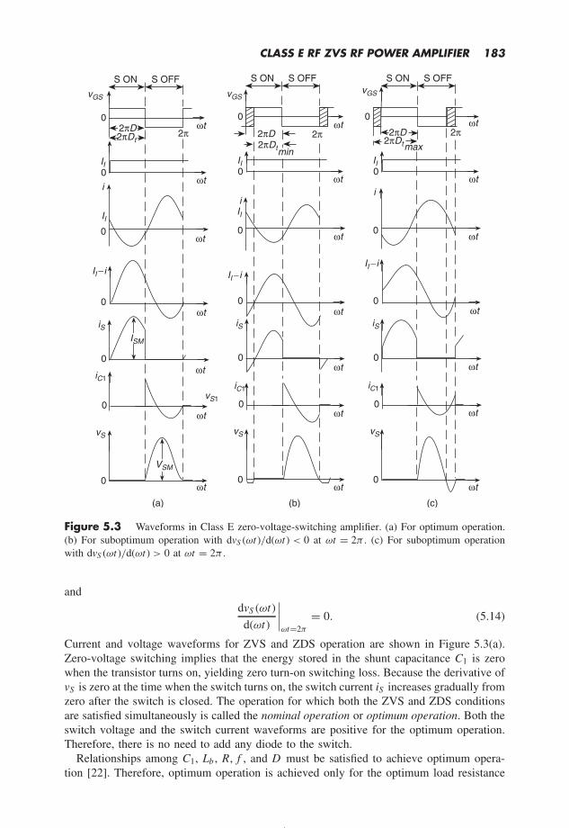
CLASS E RF ZVS RF POWER AMPLIFIER 183
(c)
ωt
2π
0
0
0
0
(a)
0
iC1
i
vS
ISM
VSM
iS
0
vGS
II
II0
2πD2πDt
S ON S OFF
vS1
ωt
(b)
ωt
0
0
0
0
0
vS
iS
0
vGS
i
II0
2πD2πDt
S ON S OFF
min
ωt
ωt
2π
0
0
0
0
0
vS
iS
0
vGS
i
II0
2πD2πDt
S ON S OFF
max
ωt2π
ωt
ωt
ωt
ωt
ωt ωt
ωt
ωt
ωt
ωt
ωt
ωtωt
ωtωt
II −i II −iII −i
2π2π
iC1 iC1
II
Figure 5.3 Waveforms in Class E zero-voltage-switching amplifier. (a) For optimum operation.(b) For suboptimum operation with dvS (ωt )/d(ωt ) < 0 at ωt = 2π . (c) For suboptimum operationwith dvS (ωt )/d(ωt ) > 0 at ωt = 2π .
anddvS (ωt)
d(ωt)
∣∣∣∣ωt=2π
= 0. (5.14)
Current and voltage waveforms for ZVS and ZDS operation are shown in Figure 5.3(a).Zero-voltage switching implies that the energy stored in the shunt capacitance C1 is zerowhen the transistor turns on, yielding zero turn-on switching loss. Because the derivative ofvS is zero at the time when the switch turns on, the switch current iS increases gradually fromzero after the switch is closed. The operation for which both the ZVS and ZDS conditionsare satisfied simultaneously is called the nominal operation or optimum operation. Both theswitch voltage and the switch current waveforms are positive for the optimum operation.Therefore, there is no need to add any diode to the switch.
Relationships among C1, Lb , R, f , and D must be satisfied to achieve optimum opera-tion [22]. Therefore, optimum operation is achieved only for the optimum load resistance

184 RF POWER AMPLIFIERS
R = Ropt . In addition, the operating frequency f for optimum operation must be locatedbetween two resonant frequencies
fo1 < f < fo2. (5.15)
If R > Ropt , the amplitude Im of the current i through the L-C -R series-resonant circuitis lower than that required for the optimum operation, the voltage drop across the shuntcapacitor C1 decreases. Also, the switch voltage vS is greater than zero at turn-on. On theother hand, if R < Ropt , the amplitude Im is higher than that required for optimum operation,the voltage drop across the shunt capacitor C1 increases, and the switch voltage vS is lessthan zero at turn-on. In both cases, assuming a linear capacitance C1, the energy stored inC1 just before turn-on of the switch is W (2π−) = 1
2 C1v 2S (2π−). This energy is dissipated
in the transistor as heat after the switch is turned on, resulting in a turn-on switching loss.To obtain the ZVS operation at a wider load range, an antiparallel or a series diode can beadded to the transistor. This improvement ensures that the switch automatically turns on atzero voltage for R ≤ Ropt .
5.5 Suboptimum Operation
In many applications, the load resistance varies over a certain range. The turn-on of theswitch at zero voltage can be achieved for suboptimum operation for 0 ≤ R ≤ Ropt . Forsuboptimum operation, vS (2π ) = 0 and either dvS (ωt)/d(ωt) < 0 or dvS (ωt)/d(ωt) > 0.Figure 5.3(b) shows the current and voltage waveforms for the case when vS (2π ) = 0 anddvS (ωt)/d(ωt) < 0 at ωt = 2π . Power MOSFETs are bidirectional switches because theircurrent can flow in both directions, but their voltage can only be greater than −0.7 V. Whenthe switch voltage reaches −0.7 V, the antiparallel diode turns on and therefore the switchautomatically turns on. The diode accelerates the time at which the switch turns on. Thistime is no longer determined by the gate-to-source voltage. Since the switch turns on at zerovoltage, the turn-on switching loss is zero, yielding high efficiency. Such an operation canbe achieved for 0 ≤ R ≤ Ropt . In addition, if R < Ropt , the operating frequency f and thetransistor ON switch duty cycle Dt can vary in bounded ranges. When the switch current isnegative, the antiparallel diode is ON, but the transistor can either be ON or OFF. Therefore,the transistor ON switch duty cycle Dt is less than or equal to the ON switch duty cycle ofthe entire switch D . When the switch current is positive, the diode is OFF and the transistormust be ON. Hence, the range of Dt is Dt min ≤ Dt ≤ D , as indicated in Figure 5.3(b) bythe shaded area.
Figure 5.3(c) depicts current and voltage waveforms for the case when vS (2π ) = 0 anddvS (ωt)/d(ωt) > 0 at ωt = 2π . Notice that the switch current iS is always positive, butthe switch voltage vS has positive and negative values. Therefore, a unidirectional switchfor current and a bidirectional switch for voltage is needed. Such a switch can be obtainedby adding a diode in series with a MOSFET. When the switch voltage vS is negative thediode is OFF and supports the switch voltage, regardless of the state of the MOSFET. TheMOSFET is turned on during the time interval when the switch voltage is negative. Oncethe switch voltage reaches 0.7 V with a positive derivative, the diode turns on, turning theentire switch on. The series diode delays the time at which the switch turns on. The rangeof Dt is D ≤ Dt ≤ Dtmax , as shown in Figure 5.3(c) by the shaded area. The disadvantagesof the switch with a series diode are higher on-voltage and higher conduction loss. Anotherdisadvantage is associated with the transistor output capacitance. When the switch voltageincreases, the transistor output capacitance is charged through the series diode to the peak

CLASS E RF ZVS RF POWER AMPLIFIER 185
value of the switch voltage and then remains at this voltage until the transistor turns on(because the diode is OFF). At this time, the transistor output capacitance is dischargedthrough the MOSFET on-resistance, dissipating the stored energy.
5.6 Analysis
5.6.1 Assumptions
The analysis of the Class E ZVS amplifier of Figure 5.1(a) is carried out under the followingassumptions:
1. The transistor and the antiparallel diode form an ideal switch whose on-resistance iszero, off-resistance is infinity, and switching times are zero.
2. The choke inductance is high enough so that the ac component is much lower than thedc component of the input current.
3. The loaded quality factor QL of the LCR series-resonant circuit is high enough so thatthe current i through the resonant circuit is sinusoidal.
4. The duty ratio D is 0.5.
5.6.2 Current and Voltage Waveforms
The current through the series-resonant circuit is sinusoidal and given by
i = Im sin(ωt + φ) (5.16)
where Im is the amplitude and φ is the initial phase of the current i . According toFigure 5.1(a),
iS + iC 1 = II − i = II − Im sin(ωt + φ). (5.17)
For the time interval 0 < ωt ≤ π , the switch is ON and therefore iC 1 = 0. Consequently,the current through the MOSFET is given by
iS =
II − Im sin(ωt + φ), for 0 < ωt ≤ π ,0, for π < ωt ≤ 2π.
(5.18)
For the time interval π < ωt ≤ 2π , the switch is OFF which implies that iS = 0. Hence,the current through the shunt capacitor C1 is given by
iC 1 =
0, for 0 < ωt ≤ π ,II − Im sin(ωt + φ), for π < ωt ≤ 2π.
(5.19)
The voltage across the shunt capacitor and the switch is
vS = vC 1 = 1
ωC1
∫ ωt
π
iC 1 d(ωt) = 1
ωC1
∫ ωt
π
[II − Im sin(ωt + φ)] d(ωt)
=
0, for 0 < ωt ≤ π ,1
ωC1II (ωt − π ) + Im [cos(ωt + φ) + cos φ], for π < ωt ≤ 2π.
(5.20)

186 RF POWER AMPLIFIERS
Substitution of the ZVS condition vS (2π ) = 0 into (5.20) produces a relationship amongII , Im , and φ:
Im = −IIπ
2 cos φ. (5.21)
Substitution of (5.21) into (5.18) yields the switch current
iSII
=
1 + π
2 cos φsin(ωt + φ), for 0 < ωt ≤ π ,
0, for π < ωt ≤ 2π.(5.22)
Likewise, substituting (5.21) into (5.19), one obtains the current through the shunt capaci-tor C1
iC 1
II=
0, for 0 < ωt ≤ π ,
1 + π
2 cos φsin(ωt + φ), for π < ωt ≤ 2π.
(5.23)
From (5.21), equation (5.20) becomes
vS =
0, for 0 < ωt ≤ π ,
II
ωC1
[ωt − 3π
2− π
2 cos φ[cos(ωt + φ)]
], for π < ωt ≤ 2π.
(5.24)
Using the condition dvS /d (ωt) = 0 at ωt = 2π , one obtains
tan φ = − 2
π(5.25)
from which
φ = π − arctan
(2
π
)= 2.5747 rad = 147.52
. (5.26)
Using trigonometric relationships,
sin φ = 2√π2 + 4
(5.27)
and
cos φ = − π√π2 + 4
. (5.28)
Substitution of (5.28) into (5.21) yields
Im =√
π2 + 4
2II ≈ 1.8621II . (5.29)
Hence,
iSII
= 1 −
√π2 + 4
2sin(ωt + φ), for 0 < ωt ≤ π ,
0, for π < ωt ≤ 2π ,(5.30)
iC 1
II=
0, for 0 < ωt ≤ π ,
1 −√
π2 + 4
2sin(ωt + φ), for π < ωt ≤ 2π ,
(5.31)
and
vS =
0, for 0 < ωt ≤ π ,
II
ωC1
(ωt − 3π
2− π
2cos ωt − sin ωt
), for π < ωt ≤ 2π.
(5.32)

CLASS E RF ZVS RF POWER AMPLIFIER 187
The dc component of the voltage across an ideal choke inductor is zero. From (5.24), thedc input voltage is found as
VI = 1
2π
∫ 2π
π
vS d(ωt) = II
2πωC1
∫ 2π
π
(ωt − 3π
2− π
2cos ωt − sin ωt
)d(ωt) = II
πωC1.
(5.33)Rearrangement of this equation produces the dc input resistance of the Class E amplifier
RDC ≡ VI
II= 1
πωC1. (5.34)
Hence,
Im =√
π2 + 4
2πωC1VI . (5.35)
Using (5.32), one arrives at the normalized switch voltage waveform
vS
VI=
0, for 0 < ωt ≤ 2π ,
π
(ωt − 3π
2− π
2cos ωt − sin ωt
), for π < ωt ≤ 2π.
(5.36)
5.6.3 Current and Voltage Stresses
Differentiating (5.22),
diSd(ωt)
= −II
√π2 + 4
2cos(ωt + φ) = 0, (5.37)
one obtains the value of ωt at which the peak value of the switch current occurs
ωtim = 3π
2− φ = 270 − 147.52 = 122.48
. (5.38)
Substitution of this into (5.22) yields the switch peak current
ISM = II
(√π2 + 4
2+ 1
)= 2.862II . (5.39)
Differentiating the switch voltage waveform vS in (5.24)
dvS
d(ωt)= πVI
[1 + π
2 cos φsin(ωt + φ)
]= 0 (5.40)
yields the trigonometric equation
sin(ωtvm + φ) = −2 cos φ
π= 2√
π2 + 4= sin φ = sin(π − φ) = sin(2π + π − φ) (5.41)
the solution of which gives the value of ωt at which the peak value of the switch voltageoccurs
ωtvm = 3π − 2φ = 3 × 180 − 2 × 147.52 = 244.96. (5.42)
Hence,
VSM = 2π (π − φ)VI = 2π (π − 2.5747)VI = 3.562VI . (5.43)
The amplitude of the voltage across the resonant capacitor C is
VCm = |XC (f )|Im = Im
ωC(5.44)

188 RF POWER AMPLIFIERS
and the amplitude of the voltage across the resonant inductor L is
VLm = XL(f )Im = ωLIm . (5.45)
Neglecting the power losses, the ac output power PO is equal to the dc input powerPI = VI II . Hence, using ISM /II and VSM /VI , one obtains the power-output capability
cp ≡ PO
ISM VSM= II VI
ISM VSM= 1
π (π − φ)(√
π2 + 4 + 2)= 1
2.862× 1
3.562= 0.0981.
(5.46)
5.6.4 Input Impedance of the Series Resonant Circuit
The current through the series-resonant circuit is sinusoidal. Consequently, higher harmonicsof the input power are zero. Therefore, it is sufficient to consider the input impedance of theseries-resonant circuit at the operating frequency f . Figure 5.4 shows an equivalent circuit ofthe series-resonant circuit above resonance at the operating frequency f . A phasor diagramof the voltages at the fundamental component is depicted in Figure 5.5. The voltage acrossthe load resistance R is
vR = iR = VRm sin(ωt + φ) (5.47)
where VRm = RIm is the amplitude of the output voltage and φ is the initial phase. Thevoltage vX across the L-C components is nonsinusoidal, equal to vX = vS − vR . The fun-damental component of the voltage across the C -La circuit is zero because the reactance ofthis circuit at the operating frequency f is zero. The fundamental component of the voltageacross the inductance Lb is
vLb1 = VLbm1 cos(ωt + φ) (5.48)
+vRR
i
vS1
Lb
+ vLb1+
Figure 5.4 Equivalent circuit of the series-resonant circuit above resonance at the operatingfrequency f .
0
VRm
φ
Vsm1
VLbm1
Figure 5.5 Phasor diagram of the voltages at the operating frequency f .

CLASS E RF ZVS RF POWER AMPLIFIER 189
where VLbm1 = ωLbIm . The fundamental component of the switch voltage, which is theinput voltage of the series-resonant circuit at the operating frequency, is given by
vs1 = vR + vLb1 = VRm sin(ωt + φ) + VLbm1 cos(ωt + φ). (5.49)
Using (5.24) and the Fourier trigonometric series formula,
VRm = 1
π
∫ 2π
π
vS sin(ωt + φ) d(ωt)
= 1
π
∫ 2π
π
VI π
[ωt − 3π
2− π
2 cos φcos(ωt + φ)
]sin(ωt + φ) d(ωt)
= 4√π2 + 4
VI ≈ 1.074VI . (5.50)
Substituting (5.24) into the Fourier formula and using (5.33), the amplitude of the funda-mental component of the voltage across the input reactance of the series-resonant circuit(equal to the reactance of the inductance Lb ) is obtained as
VLbm1 = ωLbIm = 1
π
∫ 2π
π
vS cos(ωt + φ) d(ωt)
= 1
π
∫ 2π
π
VI π
[ωt − 3π
2− π
2 cos φcos(ωt + φ)
]cos(ωt + φ) d(ωt)
= π (π2 − 4)
4√
π2 + 4VI ≈ 1.2378VI . (5.51)
5.6.5 Output Power
From (5.50), one obtains the output power
PO = V 2Rm
2R= 8
π2 + 4
V 2I
R≈ 0.5768
V 2I
R. (5.52)
5.6.6 Component Values
Combining (5.21), (5.33), and (5.50), we get
R = VRm
Im=
4√π2 + 4
VI
√π2 + 4
2πωC1VI
= 8
π (π2 + 4)ωC1(5.53)
resulting in
ωC1R = 8
π (π2 + 4)≈ 0.1836. (5.54)
Similarly, using (5.21), (5.33), and (5.51),
XLb = ωLb = VLbm1
Im=
π (π2 − 4)
4√
π2 + 4VI
√π2 + 4
2πωC1VI
= π2 − 4
2(π2 + 4)ωC1(5.55)

190 RF POWER AMPLIFIERS
producing
ω2LbC1 = π2 − 4
2(π2 + 4)≈ 0.2116. (5.56)
The ratio of (5.56) to (5.54) is
ω2LbC1
ωC1R= ωLb
R= π (π2 − 4)
16≈ 1.1525. (5.57)
From (5.7), (5.8), and (5.57), the reactance of the resonant inductor is
ωL = QLR (5.58)
and the reactance of the resonant capacitor is
XC = 1
ωC= ωLa = ω(L − Lb ) = QLR − ωLb = R
(QL − ωLb
R
)
= R
[QL − π (π2 − 4)
16
]= R (QL − 1.1525) . (5.59)
The dc input resistance of the Class E amplifier is
RDC = 1
πωC1= π2 + 4
8R ≈ 1.7337R. (5.60)
5.7 Maximum Operating Frequency
At high frequencies, the transistor output capacitance Co becomes higher than the shuntcapacitance C1 required to achieve the ZVS and ZDS operation. The maximum frequencyoccurs when C1 = Co . Assume that the transistor output capacitance Co is linear. ForD = 0.5, the maximum operating frequency fmax at which Class E ZVS and ZDS operationis achievable is determined by the condition
2π fmax CoR = 8
π (π2 + 4)(5.61)
yielding
fmax = 4
π2(π2 + 4)CoR≈ 0.02922
CoR. (5.62)
Since
R = 8
π2 + 4
V 2I
PO(5.63)
we obtain the maximum operating frequency of the Class E amplifier that satisfies both theZVS and ZDS conditions at D = 0.5
fmax = PO
2π2CoV 2I
≈ 0.05066PO
CoV 2I
. (5.64)
A higher maximum operating frequency than that given by (5.64) for D = 0.5 can beobtained when only the ZVS condition is satisfied, but the ZDS condition is not. Themaximum operating frequency of the Class E amplifier under the ZVS and ZDS conditionsincreases as the duty cycle D decreases [68]. However, at low values of D (usually forD < 0.2), the efficiency of the amplifier decreases [55]. For f > fmax , a Class CE operationcan be obtained, which offers a reasonably high efficiency [27].

CLASS E RF ZVS RF POWER AMPLIFIER 191
5.8 Choke Inductance
When the switch is ON, the voltage across the choke inductor is
vLf = VI (5.65)
and the current through the choke inductance Lf is
iLf = 1
Lf
∫ t
0vLf dt + iLf (0) = 1
Lf
∫ t
0VI dt + iLf (0) = VI
Lft + iLf (0). (5.66)
Hence,
iLf
(T
2
)= VI T
2Lf+ iLf (0) = VI
2fLf+ iLf (0). (5.67)
The peak-to-peak current ripple through the choke inductor is
iLf = iLf
(T
2
)− iLf (0) = VI
2fLf. (5.68)
Thus, the minimum choke inductance required for the maximum peak-to-peak current rip-ple is
Lfmin = VI
2f iLfmax= VI
2fIIiLfmax
II
= RDC
2fiLfmax
II
= π2 + 4
16
R
fiLfmax
II
≈ 0.86685R
fiLfmax
II
. (5.69)
For iLfmax /II = 0.1,
Lfmin = 8.6685R
f. (5.70)
An alternative method for determining Lfmin is by separating the low-frequency modulatingvoltage and the high-frequency carrier voltage in a Class E RF transmitter with amplitudemodulation (AM). The minimum value of choke inductance Lfmin to obtain the peak-to-peakcurrent ripple less than 10 % of dc current II is given by [17]
Lfmin = 2
(π2
4+ 1
)R
f≈ 7R
f. (5.71)
5.9 Summary of Parameters at D = 0.5
The parameters of the Class E ZVS amplifier for the duty cycle D = 0.5 are as follows:
iSII
= π
2sin ωt − cos ωt + 1, for 0 < ωt ≤ π ,
0, for π < ωt ≤ 2π(5.72)
vS
VI=
0, for 0 < ωt ≤ π ,
π
(ωt − 3π
2− π
2cos ωt − sin ωt
), for π < ωt ≤ 2π
(5.73)

192 RF POWER AMPLIFIERS
iC 1
II=
0, for 0 < ωt ≤ π ,π
2sin ωt − cos ωt + 1, for π < ωt ≤ 2π
(5.74)
tan φ = − 2
π(5.75)
sin φ = 2√π2 + 4
(5.76)
cos φ = − π√π2 + 4
(5.77)
φ = π − arctan
(2
π
)= 2.5747 rad = 147.52 (5.78)
RDC ≡ VI
II= 1
πωC1= π2 + 4
8R = 1.7337R (5.79)
ISM
II=
√π2 + 4
2+ 1 = 2.862 (5.80)
VSM
VI= 2π (π − φ) = 3.562 (5.81)
cp = II VI
ISM VSM= 1
π (π − φ)(2 + √π2 + 4)
= 0.0981 (5.82)
Im
II=
√π2 + 4
2= 1.8621 (5.83)
VRm
VI= 4√
π2 + 4= 1.074 (5.84)
VLbm1
VI= π (π2 − 4)
4√
π2 + 4= 1.2378 (5.85)
PO = V 2Rm
2R= 8
π2 + 4
V 2I
R= 0.5768
V 2I
R(5.86)
ωC1R = 8
π (π2 + 4)= 0.1836 (5.87)
ωLb
R= π (π2 − 4)
16= 1.1525 (5.88)
ω2LbC1 = π2 − 4
2(π2 + 4)= 0.2116 (5.89)
1
ωCR=(
QL − ωLb
R
)=[
QL − π (π2 − 4)
16
]≈ QL − 1.1525. (5.90)
5.10 Efficiency
The power losses and the efficiency of the Class E amplifier will be considered for the dutycycle D = 0.5. The current through the input choke inductor Lf is nearly constant. Hence,

CLASS E RF ZVS RF POWER AMPLIFIER 193
from (5.83) the rms value of the inductor current is
ILfrms ≈ II = 2Im√π2 + 4
. (5.91)
The amplifier efficiency is defined as ηI = PO/PI and PO = RI 2m/2. From (5.86) and (5.91),
the power loss in the dc ESR rLf of the choke inductor Lf is
PrLf = rLf I 2Lfrms = 4I 2
m rLf
(π2 + 4)= 8rLf
(π2 + 4)RPO . (5.92)
For the duty cycle D = 0.5, the rms value of the switch current is found from (5.72)
ISrms =√
1
2π
∫ π
0i 2S d(ωt) = II
√π2 + 28
4= Im
2
√π2 + 28
π2 + 4(5.93)
resulting in the switch conduction loss
PrDS = rDS I 2Srms = rDS I 2
m (π2 + 28)
4(π2 + 4)= (π2 + 28)rDS
2(π2 + 4)RPO . (5.94)
Using (5.74), the rms value of the current through the shunt capacitor C1 is
IC 1rms =√
1
2π
∫ 2π
π
i 2C 1 d(ωt) = II
√π2 − 4
4= Im
2
√π2 − 4
π2 + 4(5.95)
which leads to the power loss in the ESR rC 1 of the shunt capacitor C1
PrC 1 = rC 1I 2C 1rms = rC 1I 2
m (π2 − 4)
4(π2 + 4)= (π2 − 4)rC 1
2(π2 + 4)RPO . (5.96)
The power losses in the ESR rL of the resonant inductor L is
PrL = rLI 2m
2= rL
RPO (5.97)
and in the ESR rC of the resonant capacitor C is
PrC = rC I 2m
2= rC
RPO . (5.98)
The turn-on switching loss is zero if the ZVS condition is satisfied. The turn-off switchingloss can be estimated as follows. Assume that the transistor current during the turn-off timetf decreases linearly
iS = 2II
(1 − ωt − π
ωtf
), for π < ωt ≤ π + ωtf . (5.99)
The sinusoidal current through the resonant circuit does not change significantly duringthe fall time tf and is i ≈ 2II . Hence, the current through the shunt capacitor C1 can beapproximated by
iC 1 ≈ 2II (ωt − π )
ωtf, for π < ωt ≤ π + ωtf (5.100)
which gives the voltage across the shunt capacitor C1 and the switch
vS = 1
ωC1
∫ ωt
π
iC 1 d(ωt) = II
ωC1
(ωt)2 − 2πωt + π2
ωtf= VI π [(ωt)2 − 2πωt + π2]
ωtf.
(5.101)

194 RF POWER AMPLIFIERS
Thus, the average value of the power loss associated with the fall time tf is
Ptf = 1
2π
∫ π+ωtf
π
iS vS d(ωt) = (ωtf )2
12PI ≈ (ωtf )2
12PO . (5.102)
From (5.92), (5.94), (5.96), (5.102), (5.97), and (5.98), one obtains the overall power loss
PLS = PrLf + PrDS + PrC 1 + PrL + PrC + Ptf
= PO
[8rLf
(π2 + 4)R+ (π2 + 28)rDS
2(π2 + 4)R+ rC 1(π2 − 4)
2(π2 + 4)R+ rL + rC
R+ (ωtf )2
12
]. (5.103)
The efficiency of the Class E amplifier is given by
η ≡ PO
PI= PO
PO + PLS= 1
1 + PLS
PO
= 1
1 + 8rLf
(π2+4)R+ (π2 + 28)rDS
2(π2 + 4)R+ (π2 − 4)rC 1
2(π2 + 4)R+ rL + rC
R+ (ωtf )2
12
. (5.104)
Figure 5.6 shows a plot of the efficiency ηI as a function of R.The gate-drive power of each MOSFET that is required to charge and discharge a highly
nonlinear MOSFET input capacitance is given by
PG = fVGSm Qg (5.105)
where VGSm is the peak value of the gate-to-source voltage vGS and Qg is the gate chargeat vGS = VGSm .
0 10 20 30 40 50 60 70 800
10
20
30
40
50
60
70
80
90
100
R (Ω)
η (%
)
Figure 5.6 Efficiency of the Class E ZVS amplifier as a function of load resistance R forrLf = 0.15 , rDS = 0.85 , rL = 0.5 , rC = 0.05 , rC 1 = 0.076 , and tf = 20 ns.

CLASS E RF ZVS RF POWER AMPLIFIER 195
The power-added efficiency is
ηPAE = PO − PG
PI= PO − PG
PO + PLS. (5.106)
The power gain of the Class E ZVS amplifier at D = 0.5 is given by
kp ≡ PO
PG= 8
π2 + 4× V 2
I
RfVGSm Qg. (5.107)
The maximum efficiency of the Class E amplifier is achieved under ZVS and ZDS conditionsonly when all the components are ideal with zero parasitic resistances. However, real ClassE amplifiers are built using real components. The transistor on-resistance is nonzero, andthe inductors and capacitors have non-zero ESRs. The maximum efficiency of the ClassE amplifier with real components is obtained when the ZVS and ZDS conditions are notsatisfied. The switch voltage when the transistor turns on Vturn−on is positive, usually
Vturn−on = (0.03 − 0.15)VI . (5.108)
The derivative of the switch voltage when the switch turns on is usually slightly positive.Under these conditions, there is a non-zero switching power loss at the transistor turn-on time
Psw = 1
2fs C1V 2
turn−on . (5.109)
However, the shapes of the current waveforms and their rms values are modified so thatthe conduction losses in different components are reduced, yielding the maximum overallefficiency [69].
5.11 Design of Basic Class E Amplifier
The component values of the resonant circuit of the basic Class E amplifier shown inFigure 5.1(a) are obtained from (5.8), (5.86), (5.87), and (5.90) for optimum operation atD = 0.5:
R = 8
π2 + 4
V 2I
PO≈ 0.5768
V 2I
PO(5.110)
XC 1 = 1
ωC1= π (π2 + 4)R
8≈ 5.4466R (5.111)
XL = ωL = QLR (5.112)
XC = 1
ωC=[
QL − π (π2 − 4)
16
]R ≈ (QL − 1.1525)R. (5.113)
Suboptimum operation (i.e., for only ZVS operation) occurs for load resistance R(sub) lowerthan that given in (5.110), that is,
0 ≤ R(sub) < R. (5.114)
The Class E ZVS amplifier with the basic resonant circuit shown in Figure 5.1(a) operatessafely under short-circuit conditions.
The basic resonant circuit of Figure 5.1(a) does not have matching capability. In orderto transfer a specified amount of power PO at a specified dc voltage VI , the load resistanceR must be of the value determined by (5.110).

196 RF POWER AMPLIFIERS
Example 5.1
Design a Class E ZVS amplifier of Figure 5.1(a) to satisfy the following specifications:VI = 100 V, POmax = 80 W, and f = 1.2 MHz. Assume D = 0.5.
Solution. It is sufficient to design the amplifier for the maximum power. Using (5.86), thefull-load resistance is
R = 8
π2 + 4
V 2I
PO= 0.5768 × 1002
80= 72.1 . (5.115)
From (5.79), the dc resistance of the amplifier is
RDC = π2 + 4
8R = 1.7337 × 72.1 = 125 . (5.116)
The amplitude of the output voltage is computed from (5.84)
VRm = 4√π2 + 4
VI = 1.074 × 100 = 107.4 V. (5.117)
The maximum voltage across the switch and the shunt capacitor C1 can be calculated from(5.81) as
VSM = VC 1m = 3.562VI = 3.562 × 100 = 356.2 V. (5.118)
From (5.79), the dc input current is
II = 8
π2 + 4
VI
R= 0.5768 × 100
72.1= 0.8 A. (5.119)
The maximum switch current obtained using (5.80) is
ISM =(√
π2 + 4
2+ 1
)II = 2.862 × 0.8 = 2.29 A. (5.120)
The amplitude of the current through the resonant circuit computed from (5.83) is
Im =√
π2 + 4
2II = 1.8621 × 0.8 = 1.49 A. (5.121)
Assuming QL = 7 and using (5.58), (5.87), and (5.90), the component values of the loadnetwork are:
L = QLR
ω= 7 × 72.1
2π × 1.2 × 106= 66.9 µH (5.122)
C1 = 8
π (π2 + 4)ωR= 8
2π2(π2 + 4) × 1.2 × 106 × 72.1= 337.4 pF (5.123)
Let Co = 50 pF. Hence, the external shunt capacitance is
C1ext = C1 − Co = 337.4 − 50 = 287.4 pF. (5.124)
Pick C1ext = 270 pF and 18 pF in parallel/400 V. Next,
C = 1
ωR
[QL − π (π2 − 4)
16
] = 1
2π × 1.2 × 106 × 72.1 × (7 − 1.1525)= 314.6 pF.
(5.125)

CLASS E RF ZVS RF POWER AMPLIFIER 197
The peak voltages across the resonant capacitor C and the inductor L are
VCm = Im
ωC= 1.49
2π × 1.2 × 106 × 314.6 × 10−12= 628.07 V (5.126)
and
VLm = ωLIm = 2π × 1.2 × 106 × 66.9 × 10−6 × 1.49 = 751.57 V. (5.127)
Pick C = 330 pF/700 V.It follows from (5.71) that in order to keep the current ripple in the choke inductor
below 10 % of the full-load dc input current II , the value of the choke inductance must begreater than
Lf = 2
(π2
4+ 1
)R
f= 7 × 72.1
1.2 × 106= 420.58 µH. (5.128)
The peak voltage across the RF choke is
VLfm = VSM − VI = 356.2 − 100 = 256.2 V. (5.129)
Assume that the dc ESR of the choke Lf is rLf = 0.15 . Hence, from (5.92) the powerloss in rLf is
PrLf = rLf I 2I = 0.15 × 0.82 = 0.096 W. (5.130)
From (5.93), the rms value of the switch current is
ISrms = II
√π2 + 28
4= 0.8 × 1.5385 = 1.231 A. (5.131)
Select an International Rectifier IRF840 power MOSFET, which has VDSS = 500 V, IDmax =8 A, rDS = 0.85 , tf = 20 ns, and Qg = 63 nC. The transistor conduction power loss is
PrDS = rDS I 2Srms = 0.85 × 1.2312 = 1.288 W. (5.132)
Using (5.95), one obtains the rms current through the shunt capacitance C1
IC 1rms = II
√π2 − 4
4= 0.8 × 0.6057 = 0.485 A. (5.133)
Assuming the ESR of the capacitor C1 to be rC 1 = 76 m, one arrives at the conductionpower loss in rC 1
PrC 1 = rC 1I 2C 1rms = 0.076 × 0.4852 = 0.018 W. (5.134)
Assume the ESRs of the resonant inductor L and the resonant capacitor C to be rL = 0.5
and rC = 50 m at f = 1.2 MHz, the power losses in the resonant components are
PrL = rLI 2m
2= 0.5 × 1.492
2= 0.555 W (5.135)
PrC = rC I 2m
2= 0.05 × 1.492
2= 0.056 W. (5.136)
The drain current fall time is tf = 20 ns. Hence, ωtf = 2π × 1.2 × 106 × 20 × 10−9 =0.151 rad. From (5.102), the turn-off switching loss is
Ptf = (ωtf )2PO
12= 0.1512 × 80
12= 0.152 W. (5.137)

198 RF POWER AMPLIFIERS
The power loss (excluding the gate-drive power) is
PLS = PrLf + PrDS + PrC 1 + PrL + PrC + Ptf
= 0.096 + 1.288 + 0.018 + 0.555 + 0.056 + 0.152
= 2.165 W. (5.138)
The efficiency of the amplifier becomes
η = PO
PO + PLS= 80
80 + 2.165= 97.365 %. (5.139)
Assuming VGSm = 8 V, one obtains the gate-drive power
PG = fVGSm Qg = 1.2 × 106 × 8 × 63 × 10−9 = 0.605 W. (5.140)
The power-added efficiency (PAE) is
ηPAE = PO − PG
PI= PO − PG
PO + PLS= 80 − 0.605
80 + 2.165= 96.62 %. (5.141)
The power gain of the amplifier is
kp = PO
PG= 80
0.605= 132.23. (5.142)
The equivalent capacitance when the switch is OFF is
Ceq = CC1
C + C1= 330 × 337.4
330 + 337.4= 167 pF. (5.143)
The resonant frequencies are
fo1 = 1
2π√
LC= 1
2π√
66.9 × 10−6 × 330 × 10−12= 1.071 MHz (5.144)
and
fo2 = 1
2π√
LCeq= 1
2π√
66.9 × 10−6 × 167 × 10−12= 1.51 MHz. (5.145)
Notice that the operating frequency f = 1.2 MHz is between the resonant frequencies fo1
and fo2.
5.12 Impedance Matching Resonant Circuits
The purpose of the impedance matching network is to convert the load resistance orimpedance into the impedance required to produce the desired output power PO at thespecified supply voltage VI and the operating frequency f . According to (5.110), VI , PO ,and R are dependent quantities. In many applications, the load resistance is given and isdifferent from that given in (5.110). Therefore, there is a need for a matching circuit thatprovides impedance transformation downwards or upwards. A block diagram of the class Eamplifier with an impedance matching circuit is shown in Figure 5.7. Figure 5.8 showsvarious impedance matching resonant circuits. In the circuits shown in Figure 5.8(a) and(c), impedance transformation is accomplished by tapping the resonant capacitance C , andin the circuits shown in Figure 5.8(b) and (d) by tapping the resonant inductance L. Allthese circuits provide downward impedance transformation. The vertical inductance L2 inFigure 5.8(b) and the vertical inductance L1 in Figure 5.8(d) can be replaced by a step-upor step-down transformer, yielding additional impedance transformation. The topologies ofthese circuits are similar to the Greek letter π .

CLASS E RF ZVS RF POWER AMPLIFIER 199
C1
+vOVI
Lf
ImpedanceMatching
Circuit
Zi = R + jωLb
RL
Figure 5.7 Block diagram of the Class E amplifier with impedance matching resonant circuit.
C L1
L2C1
L
C1
C2
(a) (b)
C L2
L1C1
L
C2C1
C3
(c) (d)
C3 RL
RLRL
RL
Figure 5.8 Matching resonant circuits. (a) Resonant circuit π1a. (b) Resonant circuit π2a. (c)Resonant circuit π1b. (d) Resonant circuit π2b.
5.12.1 Tapped Capacitor Downward Impedance MatchingResonant Circuit π1a
Figure 5.9(a) shows the tapped capacitor matching circuit with downward impedance trans-formation. Its equivalent circuit is shown in Figure 5.9(b). Let us assume that the loadresistance RL is given. Using (5.110), the series equivalent resistance for optimum operationat D = 0.5 is given by
R = Rs = 8
π2 + 4
V 2I
PO≈ 0.5768
V 2I
PO. (5.146)
The components C1 and L are given by (5.111) and (5.112):
XC 1 = 1
ωC1= π (π2 + 4)R
8≈ 5.4466R (5.147)
and
XL = ωL = QLR. (5.148)
The reactance factor of the RL-C3 and Rs -Cs equivalent single-port networks is
q = RL
XC3
= XCs
Rs. (5.149)

200 RF POWER AMPLIFIERS
L
C1
C2
(a)
L Cs
C1
C2
(b)
C3 RL
RsC
Figure 5.9 Tapped capacitor impedance matching resonant circuit π1a providing downwardimpedance transformation. (a) Matching circuit π1a. (b) Equivalent circuit of the matching circuitπ1a.
Resistances Rs and RL as well as the reactances XCs and XC 3 are related by
Rs = R = RL
1 + q2= RL
1 +(
RL
XC 3
)2 (5.150)
and
XCs = XC 3
1 + 1q2
= XC 3
1 + (XC 3
RL)2
. (5.151)
Hence,
Cs = C3
(1 + 1
q2
)= C3
[1 +
(XC 3
RL
)2]
. (5.152)
Rearrangement of (5.150) gives
q =√
RL
Rs− 1. (5.153)
From (5.149) and (5.153),
XC 3 = 1
ωC3= RL
q= RL√
RL
Rs− 1
. (5.154)
Substitution of (5.153) into (5.149) yields
XCs = qRs = Rs
√RL
Rs− 1. (5.155)
Referring to Figure 5.9 and using (5.113) and (5.155), one arrives at
XC 2 = 1
ωC2= XC − XCs =
[QL − π (π2 − 4)
16
]Rs − qRs
= Rs
[QL − π (π2 − 4)
16−√
RL
Rs− 1
]. (5.156)

CLASS E RF ZVS RF POWER AMPLIFIER 201
Rs
XC32
Rsmax =
0 RL=XC3
RL=XC3
(a)XCs
XC3
XC32
0
(b)
RL
RL
Figure 5.10 Series equivalent resistance Rs and reactance XCs as functions of load resistanceRL in the circuit π1a. (a) Rs versus RL. (b) XCs versus RL.
It follows from (5.154) that the circuit shown in Figure 5.8(a) can match the resistancesthat satisfy the inequality
Rs < RL. (5.157)
Suboptimum operation is obtained for
0 ≤ Rs(sub) < Rs (5.158)
which corresponds to
RL < R(sub) < ∞. (5.159)
Expressions (5.150) and (5.151) are illustrated in Figure 5.10. As RL is increased from 0 toXC 3, Rs increases to XC 3/2, Rs reaches the maximum value Rsmax = XC 3/2 at RL = XC 3,and as RL is increased from XC 3 to ∞, Rs decreases from XC 3/2 to 0. Thus, the RL-C3
circuit acts as an impedance inverter [20] for RL > XC 3. If the optimum operation occursat RL = XC 3, then Rsmax = XC 3/2 and the amplifier operates under ZVS conditions at anyload resistance RL [28]. This is because Rs ≤ Rsmax = XC 3/2 at any values of RL. As RL
increases from 0 to ∞, XCs increases from 0 to XC 3, and Cs decreases from ∞ to C3.
Example 5.2
Design a Class E ZVS amplifier of Figure 5.1(a) to satisfy the following specifications:VI = 100 V, POmax = 80 W, RL = 150 , and f = 1.2 MHz. Assume D = 0.5.
Solution. It is sufficient to design the amplifier for full power. The required series resis-tance is
Rs = R = 8
π2 + 4
V 2I
PO= 0.5768 × 1002
80= 72.1 . (5.160)
Thus, the amplifier requires a matching circuit. The reactance factor is
q =√
RL
Rs− 1 =
√150
72.1− 1 = 1.039. (5.161)

202 RF POWER AMPLIFIERS
Hence,
XC 3 = 1
ωC3= RL
q= 150
1.039= 144.37 (5.162)
resulting in the capacitance
C3 = 1
ωXC 3= 1
2π × 1.2 × 106 × 144.37= 919 pF. (5.163)
The amplitude of the voltage across the capacitor C3 is the same as the amplitude of thevoltage across the load resistance RL. Thus,
VC 3m = VRm =√
2RLPO = √2 × 150 × 80 = 155 V. (5.164)
Pick C3 = 910 pF/200 V. Let QL = 7. Hence,
XC 2 = 1
ωC2= XC − XCs = Rs
[QL − π (π2 − 4)
16− q
]= 72.1(7 − 1.1525 − 1.039)
= 346.7 (5.165)
yielding
C2 = 1
ωXC 2= 1
2π × 1.2 × 106 × 346.7= 383 pF. (5.166)
The amplitude of the voltage across the capacitor C2 is
VC 2m = XC 2Im = 346.7 × 1.49 = 517 V. (5.167)
Select C2 = 390 pF/600 V. All other parameters are the same as those in Example 5.1.
5.12.2 Tapped Inductor Downward Impedance MatchingResonant Circuit π2a
Figure 5.11(a) shows the tapped inductor matching resonant circuit of Figure 5.8(b) thatprovides downward impedance transformation. Its equivalent circuit is depicted in Figure5.11(b). The values of Rs , XC 1, and XC for the resonant circuit can be calculated for
C1
C
(a)
C Ls
C1
L1
(b)
L2 RL
RsL
L1
Figure 5.11 Tapped inductor downward impedance matching circuit π2a. (a) Matching circuitπ2a. (b) The parallel impedance RL-L2 is converted into a series impedance Rs -Ls .

CLASS E RF ZVS RF POWER AMPLIFIER 203
optimum operation at D = 0.5 from (5.146), (5.111), and (5.113), respectively. The seriesresistance is
Rs = R = 8
π2 + 4
V 2I
PO≈ 0.5768
V 2I
PO(5.168)
XC 1 = 1
ωC1= π (π2 + 4)R
8≈ 5.4466R (5.169)
and
XC = 1
ωC=[
QL − π (π2 − 4)
16
]R ≈ (QL − 1.1525)R. (5.170)
The reactance factor of the RL-L2 and Rs -Ls equivalent single-port networks is
q = RL
XL2= XLs
Rs. (5.171)
Resistances Rs and RL as well as the reactances XLs and XL2 are related by
Rs = R = RL
1 + q2= RL
1 +(
RL
XL2
)2 (5.172)
and
XLs = XL2
1 + 1
q2
= XL2
1 +(
XL2
RL
)2 . (5.173)
Hence,
Ls = L2
1 + 1
q2
= L2
1 +(
XL3
RL
)2 . (5.174)
The reactance factor is
q =√
RL
Rs− 1. (5.175)
Hence,
XL2 = ωL2 = RL
q= RL√
RL
Rs− 1
. (5.176)
Since
QL = ωL
Rs= XL
Rs(5.177)
and
XLs = qRs (5.178)
one obtains
XL1 = ωL1 = ω(L − Ls ) = XL − XLs = (QL − q)Rs =(
QL −√
RL
Rs− 1
)Rs . (5.179)

204 RF POWER AMPLIFIERS
The range of resistances that can be matched by the circuit shown in Figure 5.8(b) is
Rs < RL. (5.180)
Suboptimum operation takes place for
0 ≤ Rs(sub) < Rs (5.181)
and consequently for
RL < R(sub) < ∞. (5.182)
It follows from (5.172) that when RL is increased from 0 to XL2, RS increases from 0 toRsmax = XL2/2, and when RL is increased from XL2 to ∞, Rs decreases from XL2/2 to 0.It is clear that the RL-L2 circuit behaves like an impedance inverter for RL > XL2. If theoptimum operation occurs at RL = XL2, then Rs = XL2/2 and the ZVS operation occurs atany load resistance [25, 30]. In this case, Rs ≤ Rsmax = XL2/2. As RL increases from 0 to∞, XLs increases from 0 to XL2, and Ls increases from 0 to L2.
The vertical inductance L2 can be replaced by a step-up or step-down transformer, pro-viding additional impedance transformation. The transformer leakage inductance can beabsorbed into the horizontal inductance L1. Figure 5.2 shows a Class E RF power amplifierwith a transformer. The impedance transformation is increased by the square of the trans-former turn ratio. The transformer leakage inductance Llp is absorbed into the inductanceL. The magnetizing inductance Lm is used as an inductor L2 connected in parallel withthe load reflected to the primary side of the transformer. The load of this circuit can be arectifier. The transformer may be used for wireless power transmission. The circuit can beused to charge a battery installed inside a person’s body.
Example 5.3
Design a Class E ZVS amplifier with the tapped inductor downward impedance matchingcircuit π2a shown in Figure 5.11(a) to satisfy the following specifications: VI = 100 V,POmax = 80 W, RL = 150 , and f = 1.2 MHz. Assume D = 0.5.
Solution. The series resistance Rs is
Rs = R = 8
π2 + 4
V 2I
PO= 0.5768 × 1002
80= 72.1 . (5.183)
A matching circuit is needed. The reactance factor is
q =√
RL
Rs− 1 =
√150
72.1− 1 = 1.039. (5.184)
The reactance XL2 is
XL2 = ωL2 = RL
q= 150
1.039= 144.37 (5.185)
resulting in the inductance
L2 = XL2
ω= 144.37
2π × 1.2 × 106= 19 µH. (5.186)
The amplitude of the voltage across the inductance L2 is the same as the amplitude of thevoltage across the load resistance RL. Thus,
VL2m = VRm =√
2RLPO = √2 × 150 × 80 = 155 V. (5.187)

CLASS E RF ZVS RF POWER AMPLIFIER 205
Let QL = 7. Hence,
XL1 = ωL1 = XL − XLs = Rs (QL − q) = 72.1(7 − 1.039) = 429.79 (5.188)
producing
L1 = XL1
ω= 429.79
2π × 1.2 × 106= 57 µH. (5.189)
The amplitude of the voltage across the inductor L1 is
VL1m = XL1Im = 429.79 × 1.49 = 640.387 V. (5.190)
All other parameters are identical to those in Example 5.1.
5.12.3 Matching Resonant Circuit π1b
Figure 5.12(a) shows the tapped capacitor downward impedance matching circuit. Thevalues of Rs , XC 1, and XL for the circuit shown in Figure 5.12(a) can be calculated foroptimum operation at D = 0.5 from (5.146), (5.111), and (5.112), respectively. The seriesresistance Rs , and the reactances of the shunt capacitance C1 and the resonant inductanceL are
Rs = 8
π2 + 4
V 2I
PO≈ 0.5768
V 2I
PO(5.191)
XC 1 = 1
ωC1= π (π2 + 4)R
8≈ 5.4466R (5.192)
andXL = QLR. (5.193)
(a)
L
C1
(b)
RpCp
L
C1
C3
RL
A
C2
L
C1
Cs
Rs
(c)
A
C2
B
B
B
Figure 5.12 Tapped capacitor downward impedance matching circuit π1b. (a) Matching circuitπ1b. (b) The series impedance RL-C3 is converted to a parallel impedance Rp -Cp . (c) The parallelimpedance Rp-XB is converted to the series impedance Rs -Cs .

206 RF POWER AMPLIFIERS
The reactance factor of the series circuit RL-C3 located to the right of point A in Figure5.12(a) is
qA = XC 3
RL= Rp
XCp. (5.194)
The series circuit RL-C3 can be converted to the parallel circuit Rp-Cp as depicted inFigure 5.12(b), using the following equations:
Rp = RL(1 + q2A) = RL
[1 +
(XC 3
RL
)2]
(5.195)
XCp = XC 3
(1 + 1
q2A
)= XC 3
[1 +
(RL
XC 3
)2]
(5.196)
and
Cp = C3
1 + 1
q2A
. (5.197)
The total capacitance to the right of point B is CB = C2 + Cp and the total reactance tothe right of point B is
1
XB= 1
XC 2+ 1
XCp. (5.198)
The parallel impedance Rp -XB can be converted to the series impedance Rs -Cs as shownin Figure 5.12(c). The conversion equations are
qB = Rp
XB= XCs
Rs(5.199)
Rs = R = Rp
1 + q2B
= Rp
1 +(
Rp
XB
)2 (5.200)
XCs = XC = XB
1 + 1
q2B
= XB
1 +(
XB
Rp
)2 . (5.201)
On the other hand, the reactance of the capacitance C is
XC = XCs =[
QL − π (π2 − 4)
16
]R ≈ (QL − 1.1525)R. (5.202)
Hence, the reactance factor of the impedance to the right of point B is
qB = XCs
Rs= XC
Rs= QL − π (π2 − 4)
16≈ QL − 1.1525. (5.203)
The parallel resistance is
Rp = R(1 + q2
B
) = R
1 +
[QL − π (π2 − 4)
16
]2
= R[(QL − 1.1525)2 + 1]. (5.204)
The reactance factor of the impedance to the right of point A is
qA =√
Rp
RL− 1. (5.205)

CLASS E RF ZVS RF POWER AMPLIFIER 207
Hence, the design equation for the reactance of the capacitor C3 is
XC 3 = 1
ωC3= qARL = RL
√R[(QL − 1.1525)2 + 1]
RL− 1. (5.206)
The parallel reactance is
XCp = XC 3
(1 + 1
q2A
)= R[(QL − 1.1525)2 + 1]√
R[(QL − 1.1525)2 + 1]
RL− 1
. (5.207)
The parallel reactance is
XB = Rp
qB= R[QL − 1.1525)2 + 1]
QL − 1.1525. (5.208)
The reactance XC 2 is given by
1
XC 2= 1
XB− 1
Xp. (5.209)
This gives the design equation for the reactance XC 2 as
XC 2 = 1
ωC2= R[(QL − 1.1525)2 + 1]
QL − 1.1525 −√
R[(QL − 1.1525)2 + 1]
RL− 1
. (5.210)
The resistances that can be matched by the above-mentioned circuit are
RL
(QL − 1.1525)2 + 1< Rs < RL. (5.211)
Suboptimum operation takes place for
Rs(sub) < Rs (5.212)
and therefore for
Rs(sub) < RL. (5.213)
Example 5.4
Design a Class E ZVS amplifier with tapped capacitor downward impedance matchingcircuit π1b depicted n Figure 5.12(a) to satisfy the following specifications: VI = 100 V,POmax = 80 W, RL = 150 , and f = 1.2 MHz. Assume D = 0.5.
Solution. Assuming QL = 7, the reactance of the capacitor C3 is calculated as
XC 3 = 1
ωC3= RL
√R[(QL − 1.1525)2 + 1]
RL− 1 = 150
√72.1[(7 − 1.1525)2 + 1]
150− 1
= 598.43 (5.214)
resulting in
C3 = 1
ωXC 3= 1
2π × 1.2 × 106 × 598.43= 221.6285 pF. (5.215)
208 RF POWER AMPLIFIERS
The amplitude of the current through the load resistance RL and the capacitance C3 is
IRm =√
2PO
RL=√
2 × 80
150= 1.067 A. (5.216)
Hence, the amplitude of the voltage across the capacitance C3 is
VC 3m = XC 3IRm = 598.43 × 1.067 = 638.32 V. (5.217)
Pick C3 = 220 pF/700 V.The reactance of the capacitor C2 is
XC 2 = 1
ωC2= R[(QL − 1.1525)2 + 1]
QL − 1.1525 −√
R[(QL − 1.1525)2 + 1]
RL− 1
= 72.1[(7 − 1.1525)2 + 1]
7 − 1.1525 −√
72.1[(7 − 1.1525)2 + 1]
150− 1
= 1365.69 (5.218)
yielding
C2 = 1
ωXC 2= 1
2π × 1.2 × 106 × 1365.69= 97.115 pF. (5.219)
The amplitude of the current through the capacitor C2 is
VC 2m =√
V 2Rm + V 2
C 3m =√
160.052 + 638.322 = 658.08 V. (5.220)
Pick C2 = 100 pF/700 V. All other parameters are the same as those in Example 5.1.
5.12.4 Matching Resonant Circuit π2b
The values of Rs , XC 1, and XC for the circuit shown in Figure 5.13(a) can be calculated foroptimum operation at D = 0.5 from (5.146), (5.111), and (5.113), respectively. The seriesresistance Rs and the reactance of the shunt capacitance C1 are
Rs = R = 8
π2 + 4
V 2I
PO≈ 0.5768
V 2I
PO(5.221)
and
XC 1 = 1
ωC1=[
QL − π (π2 − 4)
16
]R. (5.222)
The reactance factor of the series circuit RL-L2 and the equivalent parallel circuit Rp-Lp isgiven by
qA = XL2
RL= Rp
XLp. (5.223)

CLASS E RF ZVS RF POWER AMPLIFIER 209
(a)
C1
(b)
Rp
C1
C
RLL1
C1
C
Rs
(c)
L2
C
Ls
AB
LpL1
AB
B
Figure 5.13 Tapped inductor downward impedance matching resonant circuit π2b. (a) Matchingresonant circuit π2b. (b) Series impedance RL-L2 is converted into a parallel impedance Rp -Lp . (c)Parallel impedance Rp -Lp-L1 is converted into a series impedance Rs -Ls .
The parallel components are
Rp = RL(1 + q2
A
) = RL
[1 +
(XL2
RL
)2]
(5.224)
Xp = XL2
(1 + 1
q2A
)= XL2
[1 +
(RL
XL2
)2]
(5.225)
and
Lp = L2
(1 + 1
q2A
)= L2
[1 +
(RL
XL2
)2]
. (5.226)
The reactance of the components L1-Lp -Rp is
1
XB= 1
XL1+ 1
XLp. (5.227)
The series components Rs -Ls can be described by
QL = qB = Rp
Xp= XLs
Rs= XL
R(5.228)
Rs = R = Rp
1 + Q2L
= Rp
1 +(
Rp
XB
)2 (5.229)

210 RF POWER AMPLIFIERS
and
XL = Xs = XB
1 + 1
Q2L
= XB
1 +(
XB
Rp
)2 . (5.230)
The parallel resistance is
Rp = Rs (1 + q2B ) = R(1 + Q2
L ). (5.231)
Next,
qA =√
Rp
RL− 1 =
√R(Q2
L + 1)
RL− 1. (5.232)
Hence,
XL2 = qARL = RL
√R(Q2
L + 1)
RL− 1. (5.233)
The parallel reactance is
XLp = XL2
(1 + 1
q2A
)= R(Q2
L + 1)√R(Q2
L + 1)
RL− 1
. (5.234)
The parallel reactance is
XB = Rp
qB= R(Q2
L + 1)
QL. (5.235)
Using
1
XL1= 1
XB− 1
XLP(5.236)
we obtain
XL1 = ωL1 = R(Q2L + 1)
QL −√
R(Q2L + 1)
RL− 1
. (5.237)
This circuit can match resistances in the range
RL
Q2L + 1
< Rs < RL. (5.238)
Suboptimum operation takes place for
Rs(sub) < Rs (5.239)
and therefore forRs(sub) < RL. (5.240)
Example 5.5
Design a Class E ZVS amplifier with tapped inductor downward impedance matchingcircuit π2b shown in Figure 5.13(a) to satisfy the following specifications: VI = 100 V,POmax = 80 W, RL = 150 , and f = 1.2 MHz. Assume D = 0.5.
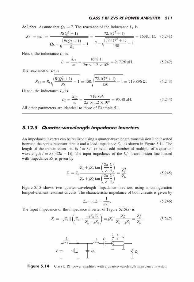
CLASS E RF ZVS RF POWER AMPLIFIER 211
Solution. Assume that QL = 7. The reactance of the inductance L1 is
XL1 = ωL1 = R(Q2L + 1)
QL −√
R(Q2L + 1)
RL− 1
= 72.1(72 + 1)
7 −√
72.1(72 + 1)
150− 1
= 1638.1 . (5.241)
Hence, the inductance L1 is
L1 = XL1
ω= 1638.1
2π × 1.2 × 106= 217.26 µH. (5.242)
The reactance of L2 is
XL2 = RL
√R(Q2
L + 1)
RL− 1 = 150
√72.1(72 + 1)
150− 1 = 719.896 . (5.243)
Hence, the inductance L2 is
L2 = XL2
ω= 719.896
2π × 1.2 × 106= 95.48 µH. (5.244)
All other parameters are identical to those of Example 5.1.
5.12.5 Quarter-wavelength Impedance Inverters
An impedance inverter can be realized using a quarter-wavelength transmission line insertedbetween the series-resonant circuit and a load impedance ZL, as shown in Figure 5.14. Thelength of the transmission line is l = λ/4 or is an odd number of multiple of a quarter-wavelength l = λ/[4(2n − 1)]. The input impedance of the λ/4 transmission line loadedwith impedance ZL is given by
Zi = Zo
ZL + jZo tan
(2π
λ
λ
4
)
Zo + jZL tan
(2π
λ
λ
4
) = Z 2o
ZL. (5.245)
Figure 5.15 shows two quarter-wavelength impedance inverters using π -configurationlumped-element resonant circuits. The characteristic impedance of both circuits is given by
Zo = ωL = 1
ωC. (5.246)
The input impedance of the impedance inverter of Figure 5.15(a) is
Zi = −jZo ||(
jZo + −jZoZL
ZL − jZo
)= jZo || Z 2
o
ZL − jZo= Z 2
o
ZL. (5.247)
L
C1
C
VI
λLf 4
ZL
Figure 5.14 Class E RF power amplifier with a quarter-wavelength impedance inverter.
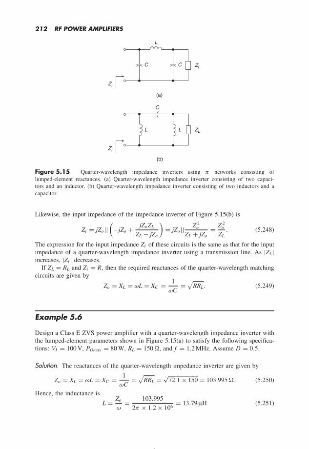
212 RF POWER AMPLIFIERS
(a)
(b)
C
L
Zi
L ZL
C
Zi
L
ZLC
Figure 5.15 Quarter-wavelength impedance inverters using π networks consisting oflumped-element reactances. (a) Quarter-wavelength impedance inverter consisting of two capaci-tors and an inductor. (b) Quarter-wavelength impedance inverter consisting of two inductors and acapacitor.
Likewise, the input impedance of the impedance inverter of Figure 5.15(b) is
Zi = jZo ||(
−jZo + jZoZL
ZL − jZo
)= jZo || Z 2
o
ZL + jZo= Z 2
o
ZL. (5.248)
The expression for the input impedance Zi of these circuits is the same as that for the inputimpedance of a quarter-wavelength impedance inverter using a transmission line. As |ZL|increases, |Zi | decreases.
If ZL = RL and Zi = R, then the required reactances of the quarter-wavelength matchingcircuits are given by
Zo = XL = ωL = XC = 1
ωC=√
RRL. (5.249)
Example 5.6
Design a Class E ZVS power amplifier with a quarter-wavelength impedance inverter withthe lumped-element parameters shown in Figure 5.15(a) to satisfy the following specifica-tions: VI = 100 V, POmax = 80 W, RL = 150 , and f = 1.2 MHz. Assume D = 0.5.
Solution. The reactances of the quarter-wavelength impedance inverter are given by
Zo = XL = ωL = XC = 1
ωC=√
RRL = √72.1 × 150 = 103.995 . (5.250)
Hence, the inductance is
L = Zo
ω= 103.995
2π × 1.2 × 106= 13.79 µH (5.251)

CLASS E RF ZVS RF POWER AMPLIFIER 213
and the capacitances are
C = 1
ωZo= 1
2π × 1.2 × 106 × 103.995= 1.2753 nF. (5.252)
All other parameters are the same as those of Example 5.1.
Figure 5.16 shows two T -type quarter-wavelength transformers made up of lumpedcomponents. These transformers are introduced here. In the circuit of Figure 5.16(a), thecapacitances C and Ct can be combined into a single capacitor. In the circuit of Figure5.16(b), the inductances L and Lt can be combined into a single inductor. The characteristicimpedance of both circuits is given by
Zo = ωL = 1
ωC. (5.253)
The input impedance of the transformer shown in Figure 5.16(a) is
Zi = −jZo + jZo(−jZo + ZL)
jZo − jZo + ZL= Z 2
o
ZL. (5.254)
The input impedance of the transformer shown in Figure 5.16(b) is
Zi = jZo + (−jZo)(jZo + ZL)
−jZo + jZo + ZL= Z 2
o
ZL. (5.255)
(a)
R vo
+
VI
L CtCRFC
C1 Lt
Ct
(b)
R vo
+
VI
L LtCRFC
C1 Ct
Lt
Figure 5.16 Quarter-wavelength impedance inverters using T -type networks consisting oflumped-element reactances. (a) Quarter-wavelength impedance inverter consisting of two capaci-tors and an inductor. (b) Quarter-wavelength impedance inverter consisting of two inductors and acapacitor.

214 RF POWER AMPLIFIERS
5.13 Push-pull Class E ZVS RF Amplifier
A push-pull Class ZVS RF power amplifier with two RF chokes is depicted in Figure 5.17[5]. The circuit with the two RF chokes can be simplified to the form depicted in Figure 5.18.This amplifier consists of two transistors, two shunt capacitors C1, RF choke, center-tappedtransformer, and series-resonant circuit driven by the secondary winding of the transformer.The transformer leakage inductance is absorbed into the resonant inductance L, and thetransistor output capacitances are absorbed into shunt capacitances C1.
Voltage and current waveforms, which explain the principle of operation of the amplifierof Figure 5.18, are depicted in Figure 5.19. The dc supply voltage source VI is connectedthrough an RF choke to the center tap of the primary winding of the output transformer.The switching transistors (MOSFETs) are driven on and off in opposite phase. The voltageacross the secondary winding consists of positive and negative Class E pulses. The series-resonant circuit filters out all harmonics, and only the voltage of the fundamental componentappears across the load resistance RL. The odd harmonics ideally are zero in all push-pullamplifiers. The amplitude of the output voltage is twice the amplitude of the single-transistorClass E amplifier. As a result, the output power increases four times.
C1
+vDS1
+vDS2C1
CL io
+vo
+vi
+vGS1
+vGS2
n :1
+vs RL
VI
VI
CB
RFC
RFC
Figure 5.17 Push-pull Class E ZVS RF power amplifier with two RF chokes [5].
VIC1
+vDS1
+vDS2C1
C
RFC
L io
II +vo
+vi
+vGS1
+vGS2
n :n :1
+vs RL
Figure 5.18 Push-pull Class E ZVS RF power amplifier.

CLASS E RF ZVS RF POWER AMPLIFIER 215
vDS2
0
vDS1
vs
0
0π 2π 3π 4π ωt
ωt
0 π 2π 3π 4π ωt
π 2π 3π 4π ωt
vo
Figure 5.19 Waveforms in push-pull Class E ZVS RF power amplifier.
The load resistance seen by each transistor across each primary winding is given by
R = n2RL (5.256)
where n is the transformer turns ratio of the number of turns of one primary winding to thenumber of turns of the secondary winding. The relationships among component values are
ωC1 = 8
π (π2 + 4)R= 8
π (π2 + 4)n2RL(5.257)
ωLb
RL= π (π2 − 4)
16and (5.258)
1
ωCRL=(
QL − ωLb
RL
)=[
QL − π (π2 − 4)
16
]. (5.259)
The output power is
PO = 32
π2 + 4
V 2I
n2RL. (5.260)
The Class E ZVS symmetrical RF power amplifiers are shown in Figure 5.20 [50, 58].The amplitudes of harmonics in the load are reduced in these amplifiers, like in push-pullamplifiers.

216 RF POWER AMPLIFIERS
VI
R
C1
VI
C1
R
C
vo+
vo+
C1
C1
L2C
(a)
RFC2
L2 2C
RFC
L
(b)
RFC2
L2
RFC
Figure 5.20 Class E ZVS symmetrical RF power amplifiers with reduced harmonics in the load.(a) Class E symmetrical amplifier with series-resonant circuit [50]. (b) Class E symmetrical amplifierwith series-parallel circuit [58].
5.14 Class E ZVS RF Power Amplifier with FiniteDC-feed Inductance
The Class E power amplifier can be operated with a finite dc-feed inductance Lf instead ofan RF choke, as shown in Figure 5.21. The output network is formed by a parallel-seriesresonant circuit. The inductance Lf and the shunt capacitance C1 form a parallel-resonantcircuit and the capacitor C and the inductor L form a series resonant circuit. This circuitis easier to integrate because the dc-feed inductance is small. A small dc-feed inductancehas a lower loss due to a smaller equivalent series resistance. In addition, if the amplifieris used as a radio transmitter with AM or any envelope modulation, it is easier to reducedistortion [17]. One such application of the Class E amplifier is in the envelope eliminationand restoration (EER) system. The current and voltage waveforms of the Class E poweramplifier with a dc-finite inductance are depicted in Figure 5.22. The peak-to-peak currentof the finite dc-feed inductance Lf increases as Lf decreases and becomes larger thanthe dc input current II . Table 5.1 gives the parameters for the Class E amplifier with a
+vo
C i
+vS
iS
R+vGS
C1
iC1 iLf
Lf
VI
L
Figure 5.21 Class E power amplifier with finite dc-feed inductance Lf .

CLASS E RF ZVS RF POWER AMPLIFIER 217
ωt
0
0
0
0
0
iC1
i
vS
ISM
VSM
iS
0
vGS
II
iLf
0
2πD
S ON S OFF
vS1
ωt
ωt
ωt
ωt
ωt
ωt
II − i
2π
Figure 5.22 Waveforms in Class E power amplifier with finite dc-feed inductance Lf .
Table 5.1 Parameters of Class E amplifier with finite DC-feedinductance.
ωLf /RDC ωLf /R ωC1R ωLb/R RPO/V 2I
∞ ∞ 0.1836 1.152 0.57681000 574.40 0.1839 1.151 0.5774
500 289.05 0.1843 1.150 0.5781200 116.02 0.1852 1.147 0.5801100 58.340 0.1867 1.141 0.583450 29.505 0.1899 1.130 0.590120 12.212 0.1999 1.096 0.610615 9.3405 0.2056 1.077 0.622710 6.4700 0.2175 1.039 0.6470
5 3.6315 0.2573 0.9251 0.72633 2.5383 0.3201 0.7726 0.84612 2.0260 0.4142 0.5809 1.01301 1.3630 0.6839 0.0007 1.36300.9992 0.7320 0.6850 0.0000 1.3650
218 RF POWER AMPLIFIERS
finite dc-feed inductance [41]. As ωLf /RDC decreases, ωCR and PO R/V 2I increase, and
ωLa/R decreases. For the last set of parameters in Table 5.1, Lb = 0, La = L, and theresonant frequency of the components L and C is equal to the operating frequency so thatω = 1/
√LC . Assuming the value of the loaded quality factor QL, these components can
be calculated from the following relationship [51]:ωL
R= 1
ωCR= QL. (5.261)
Example 5.7
Design a Class E ZVS power amplifier to satisfy the following specifications: VI = 3.3 V,POmax = 0.25 W, f = 1 GHz, and the bandwidth BW = 0.2 GHz. Assume D = 0.5.
Solution. Let us assume that ωLf /RDC = 1. The load resistance is
R = 1.363V 2
I
PO= 1.363 × 3.32
0.25= 59.372 . (5.262)
The shunt capacitance is
C1 = 0.6839
ωR= 0.6839
2π × 109 × 59.372= 1.833 pF. (5.263)
The dc feed inductance is
Lf = 1.363R
ω= 1.363 × 59.372
2π × 109= 12.879 nF. (5.264)
The loaded quality factor is
QL = foBW
= 109
0.2 × 109= 5. (5.265)
The inductance of the series-resonant circuit is
L = QLR
ω= 5 × 59.372
2π × 109= 47.246 nH. (5.266)
The capacitance of the series-resonant circuit is
C = 1
ωRQL= 1
2π × 109 × 59.372 × 5= 0.537 pF. (5.267)
The dc input resistance is
RDC = VI
II= ωLf
1= 2π × 109 × 12.879 × 10−9
1= 80.921 . (5.268)
Assuming the efficiency ηI = 0.8, we obtain the dc input power
PI = PO
ηI= 0.25
0.8= 0.3125 W (5.269)
and the dc input current
II = PI
VI= 0.3125
3.3= 94.7 mA. (5.270)

CLASS E RF ZVS RF POWER AMPLIFIER 219
5.15 Class E ZVS Amplifier with Parallel-seriesResonant Circuit
A special case of a Class E ZVS amplifier with a finite dc inductance Lf is obtained, whenthe series components L and C are resonant at the operating frequency f = ω/(2π ) [65]
ω = ωs = 1√LC
. (5.271)
The resonant frequency of the parallel-resonant circuit is
ωp = 1√Lf C1
. (5.272)
The ratio of the two resonant frequencies is
q = ωp
ωs= ωp
ω= 1
ω√
Lf C1=
√LC√
Lf C1. (5.273)
The output current is assumed to be sinusoidal
i = Im sin(ωt + φ). (5.274)
From KCL,
iLf = iS + iC 1 + i . (5.275)
When the switch is ON,
vS = 0 (5.276)
vLf = VI (5.277)
iC 1 = ωC1dvS
d(ωt)= 0 (5.278)
iLf = 1
ωLf
∫ ωt
0vLf d(ωt) + iLf (0) = 1
ωLf
∫ ωt
0VI d(ωt) + iLf (0) = VI
ωLfωt + iLf (0)
(5.279)and the switch current is given by
iS = iLf − i = VI
ωLfωt + iLf (0) − Im sin(ωt + φ) for 0 < ωt ≤ π. (5.280)
SinceiS (0) = iLf (0) − Im sin φ = 0 (5.281)
iLf (0) = Im sin φ. (5.282)
Hence,
iLf = VI
ωLfωt − Im sin φ (5.283)
andiS = VI
ωLfωt + Im [sin φ − sin(ωt + φ)] for 0 < ωt ≤ π. (5.284)

220 RF POWER AMPLIFIERS
When the switch is OFF, the switch current iS is zero, vL = VI − vS , and the current throughthe shunt capacitance C1
iC 1 = iLf − i = ωC1dvS
d(ωt)= 1
ωLf
∫ ωt
π
vL d(ωt) + iLf (π ) − Im sin(ωt + φ)
= 1
ωLf
∫ ωt
π
(VI − vS ) d(ωt) + iLf (π ) − Im sin(ωt + φ) for π < ωt ≤ 2π (5.285)
where vS (π ) = 0 and
iLf (π ) = πVI
ωLf+ Im sin φ. (5.286)
Equation (5.285) can be differentiated to obtain a linear nonhomogeneous second-orderdifferential equation
ω2Lf C1d2vS
d(ωt)2+ vS − VI − ωLf Im cos(ω + φ) = 0. (5.287)
The general solution of the differential equation is
vS
VI= A1 cos (qωt) + A2 sin (qωt) + 1 + q2p
q2 − 1cos(ωt + φ) (5.288)
where
p = ωLf Im
VI(5.289)
q = ωr
ω= 1
ω√
Lf C1(5.290)
A1 = qp
q2 − 1[q cos φ cos πq + (2q2 − 1) sin φ sin πq − cos πq − πq sin πq (5.291)
and
A2 = qp
q2 − 1[q cos φ sin πq − (2q2 − 1) sin φ cos πq + πq cos πq − sin πq . (5.292)
The three unknowns in (5.288) are: p, q , and φ. Using the ZVS and ZDS conditions forvS at ωt = 2π and the equation for the dc supply voltage
VI = 1
2π
∫ 2π
ovS d(ωt) (5.293)
one obtains the numerical solution of (5.288)
q = ωr
ω= 1
ω√
Lf C1(5.294)
p = ωLf Im
VI= 1.21 (5.295)
andφ = 195.155
. (5.296)
The dc supply current is given by
II = 1
2π
∫ 2π
0iS d(ωt) = Im
2π
(π2
2p+ 2 cos φ − π sin φ
). (5.297)

CLASS E RF ZVS RF POWER AMPLIFIER 221
The component of the switch voltage at the fundamental frequency is dropped across theload R and therefore its reactive component is zero
VX 1 = 1
π
∫ 2π
0vS cos(ωt + φ) d(ωt) = 0. (5.298)
The final results obtained from numerical solution are as follows:ωLf
R= 0.732 (5.299)
ωC1R = 0.685 (5.300)
ωL
R= 1
ωCR= QL (5.301)
tan ψ = R
ωLf− ωC1R (5.302)
ψ = 145.856 (5.303)
Vm = 0.945VI (5.304)
II = 0.826Im (5.305)
Im = 1.21II (5.306)
PO = 1.365V 2
I
R(5.307)
IDM = 2.647II (5.308)
VDSM = 3.647VI (5.309)
cp = 0.1036 (5.310)
and
fmax = 0.0798PO
CoV 2I
. (5.311)
5.16 Class E ZVS Amplifier with NonsinusoidalOutput Voltage
Figure 5.23 shows a circuit of the Class E amplifier with nonsinusoidal output voltage[18]. This circuit is obtained by replacing the resonant capacitor C in the Class E amplifierof Figure 5.1 with a blocking capacitor Cb . The loaded quality factor QL becomes low,and therefore the output voltage contains a lot of harmonics. The circuit of the Class Eamplifier shown in Figure 5.23 is able to operate under ZVS and ZDS at any duty cycleD . Waveforms in the Class E amplifier with a nonsinusoidal output voltage are shown inFigure 5.24.
From KCL,
iS = II − iC 1 − i . (5.312)
From KVL,
vS = VI + vL + vo . (5.313)

222 RF POWER AMPLIFIERS
+vOR
L
C1
Lf
VI
Cb
II
vS
+iS iC1
i
vGS
+
VI+ vL+
Figure 5.23 Class E amplifier with nonsinusoidal output voltage.
0
vGS
2πD
ωt2π
2π (1 D )
π
0
iI
ωt2ππ
ωt2ππ0
ωt2ππ0
0
ωt2ππ0
0
II
0ωt2ππ0
0
II
is
iC1
vs
Figure 5.24 Waveforms of Class E amplifier with nonsinusoidal output voltage.

CLASS E RF ZVS RF POWER AMPLIFIER 223
When the switch is ON for 0 < ωt ≤ 2πD or 0 < t ≤ t1,
vS = 0 (5.314)
iC 1 = C1dvS
d(ωt)= 0 and (5.315)
VI
s= −sLI (s) + Li (0) − RI (s) (5.316)
where i (0) is the current through the inductor L at t = 0. Under the ZVS and ZDS conditionsvS (0) = 0 and dvS (0)/dt = 0 at t = 0, iS (0) = 0 and iC 1(0) = 0. Therefore,
i (0) = −II . (5.317)
From (5.316),
i = VI
R−(
II + VI
R
)exp
(−Rωt
ωL
)(5.318)
resulting in
iS = II − i =(
II + VI
R
)exp
(−Rωt
ωL
). (5.319)
The dc supply current is obtained as
II = 1
2π
∫ 2π
0iS d(ωt) = a
1 − a
VI
R(5.320)
where
a = D + Q
2πA
[exp
(−2πAD
Q
)](5.321)
A = f0f
= 1
ω√
LC1(5.322)
Q = ω0L
R= 1
ω0C1R(5.323)
and
ω0 = 1√LC1
. (5.324)
Substitution of (5.320) into (5.319) yields the normalized switch current
iSII
= 1
a
[1 − exp
(−Aωt
Q
)]for 0 < ωt ≤ 2πD (5.325)
andiSII
= 0 for 2πD < ωt ≤ 2π. (5.326)
When the switch is OFF for 2πD < ωt ≤ 2π or t1 < t ≤ T ,
iS = 0 (5.327)
VS (s) = IC 1(s)
sC1(5.328)
IC 1(s) = I (s) + II
sC1e−st1 (5.329)

224 RF POWER AMPLIFIERS
and
VS (s) = VI
se−st1 − sLI (s) + Li (t1) e−st1 − RI (s) (5.330)
where i (t1) is the initial condition of the inductor current at t = t1. Thus,
VS (s) =
1
sC1
VI
L− II
sLC1+ si (t1)
s2 + R
Ls + 1
LC
+ II
s2C
e−st1 . (5.331)
For the oscillatory case (Q > 12 ),
VS (s) =
1
sC1
VI
L− II
sLC1+ si (t1)
(s + α)2 + ω2n
+ II
s2C
e−st1 . (5.332)
where α = R/2L and ωn = ω0
√1 − 1/4Q2. Substituting (5.320) into (5.332) and taking
the inverse Laplace transform, we obtain the normalized switch voltagevS
VI= 0 for 0 < ωt ≤ 2πD (5.333)
and
vS
VI= 1
1 − a
1 − exp
[−A(ωt − 2πD)
2Q
] [cos
(A√
4Q2 − 1(ωt − 2πD)
2Q
)
−2Q2
(1 − exp
(−2πAD
Q
))− 1√
4Q2 − 1sin
(A√
4Q2 − 1(ωt − 2πD)
2Q
)]
for 2πD < ωt ≤ 2π. (5.334)
Imposing the ZVS and ZDS conditions on the switch voltage, we obtain the relationshipamong D , Q , and A in the form of a set of two equations:
cos
[πA(1 − D)
√4Q2 − 1
Q
]
−2Q2
[1 − exp
(−2πAD
Q
)]− 1√
4Q2 − 1sin
[πA(1 − D)
√4Q2 − 1
Q
]
= exp
[πA(1 − D)
Q
](5.335)
and
tan
[πA(1 − D)
√4Q2 − 1
Q
]=√
4Q2 − 1exp
(−2πAD
Q
)− 1
exp
(−2πAD
Q+ 1
) . (5.336)
These equations can be solved numerically. For D = 0.5, the solutions for which the ZVSand ZDS conditions are satisfied and the switch voltage is nonnegative are
A = 1.6029 (5.337)

CLASS E RF ZVS RF POWER AMPLIFIER 225
andQ = 2.856. (5.338)
The output voltage is given by
vo
VI= a
a − 1+ 1
1 − a
[1 − exp
(−Aωt
2Q
)]for 0 < ωt ≤ 2πD (5.339)
andvo
VI= a
a − 1+ 1
Q(1 − a)
√Q2
[1 − exp
(−2πAD
Q
)]2
+ exp
(−2πAD
Q
)
× exp
[−A(ωt − 2πD)
2Q
]cos
[A√
4Q2 − 1(ωt − 2πD)
2Q− ψ
]
− 1√4Q2 − 1
sin
[A√
4Q2 − 1(ωt − 2πD)
1Q− ψ
]
for 2πD < ωt ≤ 2π. (5.340)
where
ψ = arctan
√4Q2 − 1
2Q2
[1 − exp
(−2πAD
Q
)]− 1
. (5.341)
The major parameters of the amplifier at the duty cycle D = 0.5 are [18]:
PO = 0.1788V 2
I
R(5.342)
RDC = VI
II= 2.7801R (5.343)
VSM = 3.1014VI (5.344)
ISM = 4.2704II (5.345)
Q = ω0L
R= 1
ω0C1R= 2.856 (5.346)
ωC1R = 0.288 (5.347)
ωL
R= 2.4083 (5.348)
cp = PO
ISM VSM= 0.0857 (5.349)
and
fmax = 1.6108PO
CoV 2I
(5.350)
where Co is the transistor output capacitance. At f = fmax , C1 = Co .
Example 5.8
Design a Class E ZVS power amplifier with nonsinusoidal output voltage to satisfy thefollowing specifications: VI = 100 V, POmax = 80 W, and f = 1.2 MHz.

226 RF POWER AMPLIFIERS
Solution. Let us assume the duty cycle D = 0.5. The load resistance is
R = 0.1788V 2
I
PO= 0.1788
1002
80= 22.35 . (5.351)
The dc input resistance seen by the power supply VI is
RDC = VI
II= 2.7801R = 2.7801 × 22.35 = 62.135 . (5.352)
Assuming the amplifier efficiency η = 0.95, the dc supply power is
PI = PO
η= 80
0.95= 84.21 W. (5.353)
Hence, the dc supply current is
II = PI
VI= 84.21
100= 0.8421 A. (5.354)
The voltage stress of the switch is
VSM = 3.1014VI = 3.1014 × 100 = 310.14 V (5.355)
and the current stress of the switch is
ISM = 4.2704II = 4.2704 × 0.8421 = 3.59 A. (5.356)
The resonant frequency is
f0 = Af = 1.6029 × 1.2 × 106 = 1.923 MHz. (5.357)
The inductance is
L = QR
ω0= 2.856 × 22.35
2π × 106 × 1.923= 5.283 µH. (5.358)
The shunt capacitance is
1
Qω0= 1
2.856 × 2π × 1.923 × 106= 28.98 nF. (5.359)
5.17 Class E ZVS Power Amplifier with ParallelResonant Circuit
Figure 5.25 shows a circuit of the Class E power amplifier with a parallel resonant circuit.This circuit is also called a Class E amplifier with only one capacitor and one inductor[11–15]. Another version of this amplifier is depicted in Figure 5.26 in which the dc supplyvoltage source VI is connected in series with the inductor L and a blocking capacitor isconnected in series with the load resistance R. The circuit of the amplifier is obtained fromthe conventional Class E ZVS power amplifier by replacing the RF choke with a dc-feedinductance and the series resonant circuit by a blocking capacitor CB . Current and voltagewaveforms are shown in Figure 5.27. The drain current waveform is an increasing rampand the voltage waveform can satisfy both ZVS and ZDS conditions. The ZVS and ZDSconditions can be satisfied at any duty cycle D . From KCL and KVL,
iS = iL + iC + i (5.360)

CLASS E RF ZVS RF POWER AMPLIFIER 227
+vORCL
VI
+vS
iC i
iS
iL
Figure 5.25 Class E amplifier with only one capacitor and one inductor.
+vORC
L
VI
+vS
iC
i
iS iL
+vGS
+
CB
VI
Figure 5.26 Another version of Class E amplifier with only one capacitor and one inductor.
and
vS = VI − vo . (5.361)
Let us consider the amplifier circuit of Figure 5.25. When the switch is ON for 0 < ωt ≤2πD or 0 < ωt ≤ t1,
vS = 0 (5.362)
vo = VI (5.363)
i = VI
R(5.364)
iC = ωCdvo
d(ωt)= 0 (5.365)
iL = 1
L
∫ ωt
0vo d(ωt) + iL(0) = 1
L
∫ ωt
0VI d(ωt) + iL(0) = VI ωt
ωL+ iL(0) (5.366)
iS = VI
R+ VI ωt
ωL+ iL(0). (5.367)
Since iS (0) = 0, iL(0) = −VI /R. Hence,
iL = VI ωt
ωL− VI
R(5.368)
and
iS = iL + i = VI ωt
ωL. (5.369)
The dc supply voltage is
II = 1
2π
∫ 2πD
0iS d(ωt) = 1
2π
∫ 2πD
0
VI ωt
ωLd(ωt) = πD2VI
ωL(5.370)

228 RF POWER AMPLIFIERS
0
0
0
0
iL
iC
0
vGS
vS
2πD
ωt
ωt
ωt
ωt
vo
2π
2π(1-D )
π
2ππ
ωt2ππ
2ππ
2ππ
0
i
ωt2ππ
0ωt2ππ
iS
Figure 5.27 Waveforms of Class E amplifier with only one capacitor and one inductor.
where 2πD = ωt1. Hence, the dc resistance seen by the dc supply voltage source is given by
RDC = VI
II= ωL
πD2. (5.371)
The normalized switch current waveform is given by
iSII
= ωt
πD2for 0 < ωt ≤ 2πD (5.372)
andiSII
= 0 for 2πD < ωt ≤ 2π. (5.373)
When the switch is OFF for 2πD < ωt ≤ 2π or ωt1 < t ≤ T ,
iS = 0 (5.374)
IL(s) + IC (s) + I (s) = 0 (5.375)

CLASS E RF ZVS RF POWER AMPLIFIER 229
I (s) = Vo(s)
R(5.376)
IC (s) = sCVo(s) − Cvo(t1) e−st1 (5.377)
IL(s) = Vo(s)
sL+ iL(t1)
se−st1 (5.378)
where vo(t1) = VI and iL(t1) = VI (t1/L − 1/R). Hence,
Vo (s) = VI
s − t1RC
+ 1
RC
s2 + s
RC+ 1
LC
. (5.379)
For the oscillatory case (Q > 12 ),
Vo (s) = VI(s2 − ω2
0t1 + 2α) e−st1
(s + α)2 + ω2n
(5.380)
whereα = 1
2RC= ω0
2Q(5.381)
andωn =
√ω2
0 − α2 = ω0
√1 − 1/4Q2. (5.382)
Thus, the normalized switch voltage isvS
VI= 0 for 0 < ωt ≤ 2πD (5.383)
andvS
VI= 1 − exp
[− A
2Q(ωt − 2πD)
]cos
[A√
4Q2 − 1
2Q(ωt − 2πD)
]
−4πAQD − 1√4Q2 − 1
sin
[A√
4Q2 − 1
2Q(ωt − 2πD)
]for 2πD < ωt ≤ 2π (5.384)
where
ω0 = 1√LC
(5.385)
A = f0f
= 1
ω√
LC(5.386)
andQ = ω0RC = R
ω0L. (5.387)
Using the ZVS and ZDS conditions for the switch voltage at ωt = 2π , we obtain a set oftwo equations:
cos
[πA(1 − D)
√4Q2 − 1
Q
]− 4πAQD − 1√
4Q2 − 1sin
[πA(1 − D)
√4Q2 − 1
Q
]
= exp
[πA(1 − D)
Q
](5.388)
and
tan
[πA(1 − D)
√4Q2 − 1
Q
]= πAD
√4Q2 − 1
πAD − Q. (5.389)

230 RF POWER AMPLIFIERS
These set of equations can be solved numerically. At D = 0.5, the solutions are
A = 1.5424 (5.390)
andQ = 1.5814. (5.391)
The output voltage waveform isvo
VI= 1 for 0 < ωt ≤ 2πD (5.392)
and
vo
VI= exp
[− A
2Q(ωt − 2πD)
]cos
[A√
4Q2 − 1
2Q(ωt − 2πD)
]
−4πAQD − 1√4Q2 − 1
sin
[A√
4Q2 − 1
2Q(ωt − 2πD)
]for 2πD < ωt ≤ 2π. (5.393)
The most important parameters of the amplifier at the duty cycle D = 0.5 are given by [15]
RDC = VI
II= 0.522R (5.394)
ISM = 4II (5.395)
VSM = 3.849VI (5.396)
PO = πADQV 2
I
R= 1.9158
V 2I
R(5.397)
A = f0f
= 1.5424 (5.398)
Q = ω0CR = R
ω0L= 1.5814 (5.399)
ωCR = 1.0253 (5.400)
ωL
R= 0.41. (5.401)
cp = PO
ISM VSM= 0.0649 (5.402)
andfmax = 0.5318
PO
CoV 2I
. (5.403)
Example 5.9
Design a Class E ZVS power amplifier with a parallel resonant circuit to satisfy the fol-lowing specifications: VI = 3.3 V, POmax = 1 W, and f = 2.4 GHz.
Solution. We will assume the duty cycle D = 0.5. The load resistance is
R = 1.9158V 2
I
PO= 1.9158 × 3.32
1= 20.86 . (5.404)

CLASS E RF ZVS RF POWER AMPLIFIER 231
The dc input resistance seen by the power supply VI is
RDC = VI
II= 0.522R = 0.522 × 20.86 = 10.89 . (5.405)
Assuming the amplifier efficiency η = 0.8, the dc supply power is
PI = PO
η= 1
0.8= 1.25 W. (5.406)
Hence, the dc supply current is
II = PI
VI= 1.25
3.3= 0.379 A. (5.407)
The voltage stress of the switch is
VSM = 3.849VI = 3.849 × 3.3 = 12.7 V (5.408)
and the current stress of the switch is
ISM = 4II = 4 × 0.379 = 1.516 A. (5.409)
The resonant frequency is
f0 = Af = 1.5424 × 2.4 × 109 = 3.7 GHz. (5.410)
The resonant inductance is
L = 0.41R
ω= 0.41 × 20.86
2π × 2.4 × 109= 0.567 nH. (5.411)
The resonant capacitance is
C = 1.0253
ωR= 1.0253
2π × 2.4 × 109 × 22.86= 2.974 pF. (5.412)
5.18 Amplitude Modulation of Class E ZVS RF PowerAmplifier
The output voltage waveform in the Class E ZVS amplifier for continuous-wave (CW)operation, i.e., without modulation, is given by
vo = Vc cos ωct . (5.413)
where ωc is the carrier angular frequency and Vc is the carrier amplitude. The amplitudeof the output voltage of the Class E ZVS RF power amplifier Vm is directly proportionalto the dc supply voltage VI . For the duty cycle D = 0.5, the output voltage amplitude is
Vc = 4√π2 + 4
VI . (5.414)
This property can be used for obtaining amplitude modulation, as proposed in [17].Figure 5.28 shows the circuit of a Class E ZVS RF power amplifier with drain amplitude
modulation [17]. The source of the modulating voltage vm is connected in series with thedc supply voltage source VI , e.g., via a transformer. The voltage waveforms in the AMClass E amplifier are shown in Figure 5.29. A modulating voltage source vm is connectedin series with the dc voltage source VI . The modulating voltage is given by
vm = Vm cos ωmt . (5.415)

232 RF POWER AMPLIFIERS
+vOR
L CRFC
+vS
vI(t )
VIfc
+vGS
C1fm
+vm
+vm
Figure 5.28 Class E ZVS RF power amplifier with drain amplitude modulation.
t
vm
(b)
vDS
(a)t
vDS
(c)t
0
vo
t
(d)
Figure 5.29 Waveforms in Class E ZVS RF power amplifier with drain amplitude modulation.(a) CW drain-to-source voltage vDS . (b) Modulating voltage vm . (c) AM drain-to-source voltage vDS .(d) AM output voltage vo .
Therefore, the supply voltage of the amplifier with amplitude modulation is
vI (t) = VI + vm (t) = VI + Vm cos ωmt . (5.416)
The amplitude of the output voltage is
Vm (t) = 4√π2 + 4
[VI + vm (t)] = 4√π2 + 4
(VI + Vm cos ωmt). (5.417)
The switch voltage is vS = 0 for 0 < ωct ≤ π and
vS = (VI + Vm cos ωmt)π
(ωct + 3π
2− π
2cos ωct − sin ωct
)for π < ωc t ≤ 2π.
(5.418)

CLASS E RF ZVS RF POWER AMPLIFIER 233
Assuming an ideal bandpass filter of the Class E amplifier, the output voltage waveform is
vo = Vm (t) cos ωc t = 4√π2 + 4
(VI + Vm cos ωmt) cos ωct
= 4√π2 + 4
VI (1 + m cos ωmt) cos ωc t = Vc(1 + m cos ωmt) cos ωc t (5.419)
where the modulation index is
m = Vm
VI. (5.420)
The output voltage waveform can be rearranged to the form
vo = Vc cos ωct + mVc
2cos(ωc − ωm )t + mVc
2cos(ωc + ωm )t . (5.421)
In reality, the voltage transfer function of the series-resonant circuit in the Class E amplifierunder ZVS and ZDS conditions is not symmetrical with respect to the carrier frequency.The carrier frequency fc is higher than the resonant frequency of the series-resonant circuitfr (i.e., fc > fr ). Therefore, the two sideband components are transmitted from the drain tothe load resistance R with different magnitudes and different phase shifts (i.e., delays). Theupper sideband is attenuated more than the lower sideband. In addition, the phase shift ofthe upper sideband is more negative than that of the lower sideband. The phase shift of thelower sideband may become even positive. These effects cause harmonic distortion of theenvelope of the AM output voltage [17].
5.19 Summary
• The Class E ZVS RF power amplifier is defined as the circuit in which a single transistoris used and is operated as a switch, the transistor turns on at zero voltage, and the transistormay turn on at zero derivative.
• The transistor output capacitance, the choke parasitic capacitance, and the stray capaci-tance are absorbed into the shunt capacitance C1 in the Class E ZVS power amplifier.
• The turn-on switching loss is zero.
• The operating frequency f is greater than the resonant frequency f0 = 1/(2π√
LC ) ofthe series-resonant circuit. This results in an inductive load for the switch when it is ON.
• The antiparallel diode of the switch turns off at low di/dt and zero voltage, reducingreverse-recovery effects. Therefore, the MOSFET body diode can be used and there isno need for a fast diode.
• Zero-voltage-switching operation can be accomplished in the basic topology for loadresistances ranging from zero to Ropt . Matching circuits can be used to match anyimpedance to the desired load resistance.
• The peak voltage across the transistor is about four times higher than the input dc voltage.Therefore, the circuit is suitable for low input voltage applications.
• The drive circuit is easy to build because the gate-to-source voltage of the transistor isreferenced to ground.
• The circuit is very efficient and can be operated at high frequencies.

234 RF POWER AMPLIFIERS
• The large choke inductance with a low current ripple can be replaced by a low inductancewith a large current ripple. In this case, the equations describing the amplifier operationwill change [24].
• The loaded quality factor of the resonant circuit can be small. In the extreme case, theresonant capacitor becomes a large dc-blocking capacitor. The mathematical descriptionwill change accordingly [18].
• The maximum operating frequency of Class E operation with ZVS and ZDS or withZVS only is limited by the output capacitance of the switch and is given by (5.62).
• The maximum operating frequency of the Class E power amplifier increases as the dutycycle decreases.
5.20 References
[1] N. O. Sokal and A. D. Sokal, ‘Class E – A new class of high-efficiency tuned single-endedswitching power amplifiers,’ IEEE J. Solid-State Circuits, vol. SC-10, pp. 168–176, June 1975.
[2] N. O. Sokal and A. D. Sokal, ‘High efficiency tuned switching power amplifier,’ US Patent no.3, 919, 656, November 11, 1975.
[3] J. Ebert and M. Kazimierczuk, ‘High efficiency RF power amplifier,’ Bull. Acad. Pol. Sci., Ser.Sci. Tech., vol. 25, no. 2, pp. 13–16, February 1977.
[4] N. O. Sokal, ‘Class E can boost the efficiency,’ Electronic Design, vol. 25, no. 20, pp. 96–102,September 27, 1977.
[5] F. H. Raab, ‘Idealized operation of the Class E tuned power amplifier,’ IEEE Trans. CircuitsSyst., vol. CAS-24, pp. 725–735, December 1977.
[6] N. O. Sokal and F. H. Raab, ‘Harmonic output of Class E RF power amplifiers and loadcoupling network design,’ IEEE J. Solid-State Circuits, vol. SC-12, pp. 86–88, February 1977.
[7] F. H. Raab, ‘Effects of circuit variations on the Class E tuned power amplifier,’ IEEE J.Solid-State Circuits, vol. SC-13, pp. 239–247, April 1978.
[8] F. H. Raab and N. O. Sokal, ‘Transistor power losses in the Class E tuned power amplifier,’IEEE J. Solid-State Circuits, vol. SC-13, pp. 912–914, December 1978.
[9] N. O. Sokal and A. D. Sokal, ‘Class E switching-mode RF power amplifiers – Low power dissi-pation, low sensitivity to component values (including transistors) and well-defined operation,’RF Design, vol. 3, pp. 33–38, no. 41, July/August 1980.
[10] J. Ebert and M. K. Kazimierczuk, ‘Class E high-efficiency tuned oscillator,’ IEEE J. Solid-StateCircuits, vol. SC-16, pp. 62–66, April 1981.
[11] N. O. Sokal, ‘Class E high-efficiency switching-mode tuned power amplifier with only oneinductor and only one capacitor in load network – Approximate analysis,’ IEEE J. Solid–StateCircuits, vol. SC-16, pp. 380–384, August 1981.
[12] M. K. Kazimierczuk, ‘Effects of the collector current fall time on the Class E tuned poweramplifier,’ IEEE J. Solid-State Circuits, vol. SC-18, no. 2, pp. 181–193, April 1983.
[13] M. K. Kazimierczuk, ‘Exact analysis of Class E tuned power amplifier with only one inductorand one capacitor in load network,’ IEEE J. Solid-State Circuits, vol. SC-18, no. 2, pp. 214–221,April 1983.
[14] M. K. Kazimierczuk, ‘Parallel operation of power transistors in switching amplifiers,’ Proc.IEEE, vol. 71, no. 12, pp. 1456–1457, December 1983.
[15] M. K. Kazimierczuk, ‘Charge-control analysis of Class E tuned power amplifier,’ IEEE Trans.Electron Devices, vol. ED-31, no. 3, pp. 366–373, March 1984.
[16] B. Molnar, ‘Basic limitations of waveforms achievable in single-ended switching-mode(Class E) power amplifiers,’ IEEE J. Solid-State Circuits, vol. SC-19, no. 1, pp. 144–146,February 1984.
[17] M. K. Kazimierczuk, ‘Collector amplitude modulation of the Class E tuned power amplifier,’IEEE Trans. Circuits Syst., vol. CAS-31, no. 6, pp. 543–549, June 1984.

CLASS E RF ZVS RF POWER AMPLIFIER 235
[18] M. K. Kazimierczuk, ‘Class E tuned power amplifier with nonsinusoidal output voltage,’ IEEEJ. Solid-State Circuits, vol. SC-21, no. 4, pp. 575–581, August 1986.
[19] M. K. Kazimierczuk, ‘Generalization of conditions for 100-percent efficiency and nonzerooutput power in power amplifiers and frequency multipliers,’ IEEE Trans. Circuits Syst., vol.CAS-33, no. 8, pp. 805–506, August 1986.
[20] M. K. Kazimierczuk and K. Puczko, ‘Impedance inverter for Class E dc/dc converters,’ 29thMidwest Symposium on Circuits and Systems, Lincoln, Nebraska, August 10–12, 1986, pp.707–710.
[21] G. Luttke and H. C. Reats, ‘High voltage high frequency Class-E converter suitable for minia-turization,’ IEEE Trans. Power Electronics, vol. PE-1, pp. 193–199, October 1986.
[22] M. K. Kazimierczuk and K. Puczko, ‘Exact analysis of Class E tuned power amplifier at any Qand switch duty cycle,’ IEEE Trans. Circuits Syst., vol. CAS-34, no. 2, pp. 149–159, February1987.
[23] G. Luttke and H. C. Reats, ‘220 V 500 kHz Class E converter using a BIMOS,’ IEEE Trans.Power Electronics, vol. PE-2, pp. 186–193, July 1987.
[24] R. E. Zulinski and J. W. Steadman, ‘Class E power amplifiers and frequency multipliers withfinite dc-feed inductance,’ IEEE Trans. Circuits Syst., vol. CAS-34, no. 9, pp. 1074–1087,September 1987.
[25] C. P. Avratoglou, N. C. Voulgaris, and F. I. Ioannidou, ‘Analysis and design of a generalizedClass E tuned power amplifier,’ IEEE Trans. Circuits Syst., vol. CAS-36, no. 8, pp. 1068–1079,August 1989.
[26] M. K. Kazimierczuk and X. T. Bui, ‘Class E dc-dc converters with a capacitive impedanceinverter,’ IEEE Trans. Industrial Electronics, vol. IE-36, pp. 425–433, August 1989.
[27] M. K. Kazimierczuk and W. A. Tabisz, ‘Class C-E high-efficiency tuned power amplifier,’IEEE Trans. Circuits Syst., vol. CAS-36, no. 3, pp. 421–428, March 1989.
[28] M. K. Kazimierczuk and K. Puczko, ‘Power-output capability of Class E amplifier at any loadedQ and switch duty cycle,’ IEEE Trans. Circuits Syst., vol. CAS-36, no. 8, pp. 1142–1143,August 1989.
[29] M. K. Kazimierczuk and X. T. Bui, ‘Class E dc/dc converters with an inductive impedanceinverter,’ IEEE Trans. Power Electronics, vol. PE-4, pp. 124–135, January 1989.
[30] M. K. Kazimierczuk and K. Puczko, ‘Class E tuned power amplifier with antiparallel diode orseries diode at switch, with any loaded Q and switch duty cycle,’ IEEE Trans. Circuits Syst.,vol. CAS-36, no. 9, pp. 1201–1209, September 1989.
[31] M. K. Kazimierczuk and X. T. Bui, ‘Class E amplifier with an inductive impedance inverter,’IEEE Trans. Industrial Electronics, vol. IE-37, pp. 160–166, April 1990.
[32] G. H. Smith and R. E. Zulinski, ‘An exact analysis of Class E amplifiers with finite dc-feedinductance,’ IEEE Transactions on Circuits and Systems, vol. 37, no. 7, pp. 530–534, April1990.
[33] R. E. Zulinski and K. J. Grady, ‘Load-independent Class E power inverters: Part I – Theoreticaldevelopment,’ IEEE Trans. Circuits Syst., vol. CAS-37, pp. 1010–1018, August 1990.
[34] K. Thomas, S. Hinchliffe, and L. Hobson, ‘Class E switching-mode power amplifier for high-frequency electric process heating applications,’ Electron. Lett., vol. 23, no. 2, pp. 80–82,January 1987.
[35] D. Collins, S. Hinchliffe, and L. Hobson, ‘Optimized Class-E amplifier with load variation,’Electron. Lett., vol. 23, no. 18, pp. 973–974, August 1987.
[36] D. Collins, S. Hinchliffe, and L. Hobson, ‘Computer control of a Class E amplifier,’ Int. J.Electron., vol. 64, no. 3, pp. 493–506, 1988.
[37] S. Hinchliffe, L. Hobson, and R. W. Houston, ‘A high-power Class E amplifier for high fre-quency electric process heating,’ Int. J. Electron., vol. 64, no. 4, pp. 667–675, 1988.
[38] M. K. Kazimierczuk, ‘Synthesis of phase-modulated dc/dc inverters an dc/dc converters,’ IEEProceedings, Part B, Electric Power Applications, vol. 39, pp. 604–613, June 1992.
[39] S. Ghandi, R. E. Zulinski, and J. C. Mandojana, ‘On the feasibility of load-independent outputcurrent in Class E amplifiers,’ IEEE Trans. Circuits Syst., vol. CAS-39, pp. 564–567, July 1992.
[40] M. J. Chudobiak, ‘The use of parasitic nonlinear capacitors in Class-E amplifiers,’ IEEE Trans.Circuits Syst.-I, vol. CAS-41, no. 12, pp. 941–944, Dec. 1994.

236 RF POWER AMPLIFIERS
[41] C.-H. Li and Y.-O. Yam, ‘Maximum frequency and optimum performance of class E poweramplifier,’ IEE Proc. Circuits Devices Syst., vol. 141, no. 3, pp. 174–184, June 1994.
[42] M. K. Kazimierczuk and D. Czarkowski, Resonant Power Converters, John Wiley & Sons, NewYork, NY, 1995.
[43] T. Sawlati, C. Andre, T. Salama, J. Stich, G. Robjohn, and D. Smith, ‘Low voltage highefficiency GaAs Class E power amplifiers,’ IEEE J. Solid-State Circuits, vol. 30, pp. 1074–1080,October 1995.
[44] B. Grzesik, Z. Kaczmarczyk, and J. Janik, ‘A Class E inverter – the influence of inverterparameters on its characteristics,’ 27th IEEE Power Electronics Specialists Conference, June23–27 1996, pp. 1832–1837.
[45] S. H.-L. Tu and C. Toumazou, ‘Low distortion CMOS complementary Class-E RF tuned poweramplifiers,’ IEEE Transactions on Circuits and Systems-I, vol. 47, pp. 774–779, May 2000.
[46] W. H. Cantrell, ‘Tuning analysis for the high-Q Class-E power amplifier,’ IEEE Trans.Microwave Theory and Techniques, vol. 48, no. 12, pp. 23-97-2402, December 2000.
[47] A. J. Wilkinson and J. K. A. Everard, ‘Transmission-line load network topology for Class-E power amplifiers,’ IEEE Trans. Microwave Theory and Techniques, vol. 49, no. 6, pp.1202–1210, June 2001.
[48] K. L. Martens and M. S. Steyaert, ‘A 700-MHz 1-W fully differential CMOS Class-E poweramplifier,’ IEEE J. Solid-State Circuits, vol. 37, pp. 137–141, February 1995.
[49] F. H. Raab, P. Asbec, S. Cripps, P. B. Keningtopn, Z. B. POpovic, N. Potheary, J. Savic, andN. O. Sokal, ‘Power amplifiers and transistors for RF and microwaves,’ IEEE Transactions onMicrowave Theory and Technique, vol. 50, no. 3, pp. 814–826, March 2002.
[50] S.-W. Ma, H. Wong, and Y.-O. Yam, ‘Optimal design of high output power Class E amplifier,’Proc 4-th Int. Caracas Conf. Devices, Circuits Syst., pp. 012-1-012-3, 2002.
[51] A. V. Grebennikov and H. J. Jaeger, ‘Class E amplifier with parallel circuit – A new challengefor high-efficiency RF and microwave power amplifiers,’ IEEE MTT-S Inst. Microwave Symp.Dig., vol. 3, pp. 1627–1630, 2002.
[52] S. D. Kee, I. Aoki, A. Hajimiri, and D. Rutledge, ‘The Class-E/F family of ZVS switch-ing amplifiers,’ IEEE Transactions on MIcrowave Theory and Technique, vol. 51, no. 6, pp.1677–1690, June 2003.
[53] T. Suetsugu and M. K. Kazimierczuk, ‘Comparison of Class E amplifier with nonlinear andlinear shunt capacitances,’ IEEE Trans. Circuits Syst.-I, Fundamental Theory and Applications,vol. 50, no. 8, pp. 1089–1097, August 2003.
[54] T. Suetsugu and M. K. Kazimierczuk, ‘Analysis and design of Class E amplifier with shuntcapacitance composed of linear and nonlinear capacitances,’ IEEE Transaction on Circuits andSystems - I: Regular Papers, vol. 51, no. 7, pp. 1261–1268, July 2004.
[55] D. Kessler and M. K. Kazimierczuk, ‘Power losses of Class E power amplifier at any dutycycle,’ IEEE Trans. Circuits Syst.-I, Regular Papers, vol. 51, no. 9, pp. 1675–1689, September2004.
[56] T. Suetsugu and M. K. Kazimierczuk, ‘Design procedure of lossless voltage-clamped ClassE amplifier with transformer and diode,’ IEEE Trans. Power Electronics, vol. 20, no. 1, pp.56–64, January 2005.
[57] M. K. Kazimierczuk, V. G. Krizhanovski, J. V. Rossokhina, and D. V. Chernov, ‘Class-EMOSFET tuned power oscillator design procedure,’ IEEE Trans. Circuits and Syst.-I, RegularPapers, vol. 52, no. 6, pp. 1138–1147, June 2005.
[58] S.-C. Wong and C. K. Tse, ‘Design of symmetrical Class E power amplifiers for low harmoniccontent applications,’ IEEE Transactions on Circuits and Systems-I: Regular Papers, vol. 52,pp. 1684–1690, August 2005.
[59] T. Suetsugu and M. K. Kazimierczuk, ‘Design procedure of Class E amplifier for off-nominaloperation at 50 % duty ratio,’ IEEE Transaction on Circuits and Systems - I: Regular Paper,vol. 53, no. 7, pp. 1468–14, July 2006.
[60] Z. Kaczmarczyk,‘High-efficiency Class E, EF2, and EF3 inverters,’ IEEE Transactions on Indus-trial Electronics, vol. 53, no. 5, pp. 1584–1593, October 2006.

CLASS E RF ZVS RF POWER AMPLIFIER 237
[61] V. G. Krizhanovski, D. V. Chernov, and M. K. Kazimierczuk, ‘Low-voltage self-oscillatingClass E electronic ballast for fluorescent lamps,’ IEEE International Symposium on Circuitsand Systems, Island of Kos, Greece, May 21–24, 2006.
[62] K-C. Tsai and P. R. Gray, ‘A 1.9-GHz, 1-W CMOS Class-E power amplifier for wirelesscommunications,’ IEEE J. Solid-State Circuits, vol. 34. no. 7, pp. 962–970, July 1999.
[63] C. Yoo and Q. Huang, ‘A common-gate switched 0.9-W Class-E power amplifier with 41 %PAE in 0.25 µm CMOS,’ IEEE J. Solid-State Circuits, vol. 36. no. 5, pp. 823–830, May 2001.
[64] K. L. R. Mertens and M. S. J. Steyaert, ‘A 700-MHz, 1-W fully differential CMOS Class-Epower amplifier,’ IEEE J. Solid-State Circuits, vol. 37. no. 2, pp. 137–141, February 2002.
[65] A. V. Grebennikov and H. Jaeger, ‘Class E with parallel circuit – A new challenges for high-efficiency RF and microwave power amplifiers,’ em IEEE MTT-S Int. Microwave Symp. Dig.,2002, TJ2D-1, pp. 1627–1630.
[66] T. Suetsugu and M. K. Kazimierczuk, ‘Off-nominal operation of Class-E amplifier at anyduty cycle,’ IEEE Transactions on Circuits and Systems-I: Regular Papers, vol. 54, no. 6, pp.1389–1397, June 2007.
[67] A. V. Grebennikov and N. O. Sokal, Switchmode RF Power Amplifiers, Elsevier, Newnes,Oxford, UK, 2007.
[68] T. Suetsugu and M. K. Kazimierczuk, ‘Maximum operating frequency of Class E power ampli-fier with any duty cycle,’ IEEE Transactions on Circuits and Systems-II, 2008.
[69] N. O. Sokal, ‘Correction to ‘Optimum’ turn-on switching conditions for Class-E RF/microwavepower amplifier,’ IEEE Trans. Microwave Theory and Techniques, 2008.
5.21 Review Questions
5.1 What is the ZVS technique?
5.2 Is the transistor output capacitance absorbed into the Class E ZVS inverter topology?
5.3 Is it possible to obtain the ZVS operation at any load using the basic topology of theClass E ZVS inverter?
5.4 Is the turn-on switching loss zero in the Class E ZVS inverter?
5.5 Is the turn-off switching loss zero in the Class E ZVS inverter?
5.6 Is it possible to achieve the ZVS condition at any operating frequency?
5.7 Is the basic Class E ZVS inverter short-circuit proof?
5.8 Is the basic Class E ZVS inverter open-circuit proof?
5.9 Is it possible to use a finite dc-feed inductance in series with the dc input voltagesource VI ?
5.10 Is it required to use a high value of the loaded quality factor of the resonant circuitin the Class E ZVS inverter?
5.22 Problems
5.1 Design a Class E RF power amplifier for wireless communication applications to meetthe following specifications: VI = 3.3 V, PO = 1 W, f = 1 GHz, Co = 1 pF, QL = 5,

238 RF POWER AMPLIFIERS
rDS = 0.01 , rLf = 0.012 , rC 1 = 0.08 , rC = 0.05 , rL = 0.1 , and tf = 0. Findthe component values, reactances of reactive components, component stresses, andefficiency.
5.2 The Class E RF power amplifier given in Problem 5.1 had a load resistance RL = 50 .Design the impedance matching circuit.
5.3 Design an optimum Class E ZVS inverter to meet the following specifications: PO =125 W, VI = 48 V, and f = 2 MHz. Assume QL = 5.
5.4 The rms value of the US utility voltage is from 92 to 132 V. This voltage is rectifiedby a bridge peak rectifier to supply a Class E ZVS inverter that is operated at a switchduty cycle of 0.5. What is the required value of the voltage rating of the switch?
5.5 Repeat Problem 5.4 for the European utility line, whose rms voltage is 220 ± 15 %.
5.6 Derive the design equations for the component values for the matching resonant circuitπ2a shown in Figure 5.8(b).
5.7 Find the maximum operating frequency at which pure Class E operation is still achiev-able for VI = 200 V, PO = 75 W, and Cout = 100 pF.
5.8 Design a Class E power amplifier for wireless communications applications to meet thefollowing specifications: VI = 12 V, PO = 10 W, f = 2.4 GHz, Co = 1 pF, QL = 10,rDS = 0.01, rLf = 0.01, rC 1 = 0.08, rC = 0.01, rL = 0.1, and tf = 0. Find the compo-nent values, reactances of reactive components, component stresses, component losses,and efficiency.
5.9 The Class E amplifier given in Problem 5.8 has RL = 50. Design the impedance match-ing circuit.

6Class E Zero-current-switching RF PowerAmplifier
6.1 Introduction
In this chapter, a Class E RF zero-current switching (ZCS) power amplifier [1–4] ispresented and analyzed. In this amplifier, the switch is turned off at zero current, yieldingzero turn-off switching loss. A shortcoming of the Class E ZCS amplifier is that the switchoutput capacitance is not included in the basic amplifier topology. The switch turns on ata nonzero voltage, and the energy stored in the switch output capacitance is dissipated inthe switching device, reducing the efficiency. Therefore, the upper operating frequency ofthe Class E ZCS amplifier is lower than that of the Class E ZVS amplifier.
6.2 Circuit Description
A circuit of a Class E ZCS RF power amplifier is depicted in Figure 6.1(a). This circuitwas introduced in [1]. It consists of a single transistor and a load network. The transistoroperates cyclically as a switch at the desired operating frequency f = ω/(2π ). The simplesttype of load network consists of a resonant inductor L1 connected in series with the dcsource VI , and an L-C -R series-resonant circuit. The resistance R is an ac load.
The equivalent circuit of the Class E ZCS amplifier is shown in Figure 6.1(b). Thecapacitance C is divided into two series capacitances, Ca and Cb , so that capacitance Ca
is series resonant with L at the operating frequency f = ω/2π
ω = 1√LCa
. (6.1)
RF Power Amplifiers Marian K. Kazimierczuk 2008 John Wiley & Sons, Ltd

240 RF POWER AMPLIFIERS
L
vXiS + +
R vo
C
VI
io
(a)
iL1L1
vXiS + +
R voVI
io
(b)
iL1L1 L
vL1++vS
Ca Cb
vL1++vS
rDS
Figure 6.1 Class E RF zero-current-switching amplifier. (a) Circuit. (b) Equivalent circuit.
The additional capacitance Cb signifies the fact that the operating frequency f islower than the resonant frequency of the series-resonant circuit when the switch is ON
fo1 = 1/(2π√
LC ). The loaded quality factor QL is defined by the expression
QL = XCr
R= Ca + Cb
ωRCaCb. (6.2)
The choice of QL involves the usual tradeoff among (1) low harmonic content of the powerdelivered to R (high QL), (2) low change of amplifier performance with frequency (lowQL), (3) high efficiency of the load network (low QL), and (4) high bandwidth (low QL).
6.3 Principle of Operation
The equivalent circuit of the amplifier is shown in Figure 6.1(b). It is based on the followingassumptions:
(1) The elements of the load network are ideal.
(2) The loaded quality factor QL of the series-resonant circuit is high enough that the outputcurrent is essentially a sinusoid at the operating frequency.
(3) The switching action of the transistor is instantaneous and lossless; the transistor haszero output capacitance, zero saturation resistance, zero saturation voltage, and infinite‘off’ resistance.
It is assumed for simplicity that the switch duty ratio is 50 %, that is, the switch is ON
for half of the ac period and OFF for the remainder of the period. However, the duty ratiocan be any arbitrarily chosen if the circuit component values are chosen to be appropriatefor the chosen duty ratio. It will be explained in Section 6.4 that a duty ratio of 50 % isone of the conditions for optimum amplifier operation. The amplifier operation is deter-mined by the switch when it is closed and by the transient response of the load networkwhen the switch is open. The principle of operation of the amplifier is explained by thecurrent and voltage waveforms, which are shown in Figure 6.2. Figure 6.2(a) depicts thewaveforms for optimum operation. When the switch is open, its current iS is zero. Hence,the inductor current iL1 is equal to a nearly sinusoidal output current i . The current iL1

CLASS E ZCS RF POWER AMPLIFIER 241
vL1
0
00
iL1
0
Open Closed
ωt
ωt
ωt
io
vS
2ππ0
2ππ
2ππ0
iS
02ππ0 ωt
π ωt0 2π
VI
0π ωt0 2π
0π ωt2π
Switch
vGS
vL1
0
00
iL1
0
Open Closed
ωt
ωt
ωt
io
vS
2ππ0
2ππ
2π
2π
π0
iS
0π0 ωt
π ωt0 2π
VI
0π ωt0 2π
0π ωt2π
Switch
vGS
(a) (b)
Figure 6.2 Current and voltage waveforms in the Class E ZCS amplifier. (a) For optimum oper-ation. (b) For suboptimum operation.

242 RF POWER AMPLIFIERS
produces the voltage drop vL1 across the inductor L1. This voltage is approximately asection of a sine wave. The difference between the supply voltage VI and the voltage vL1
is the voltage across the switch vS . When the switch is closed, the voltage vS is zero,and voltage vL1 equals the supply voltage VI . This voltage produces the linearly increas-ing current iL1. The difference between the current iL1 and current i flows through theswitch.
In the Class E ZCS amplifier, it is possible to eliminate power losses due to on-to-offtransition of the transistor, yielding high efficiency. Assuming that the transistor is turnedoff at ωtoff = 2π , the ZCS condition at turn-off is
iS (2π ) = 0. (6.3)
For optimum operation, the zero-derivative switching (ZDS) condition should alsobe satisfied:
diSd(ωt)
∣∣∣∣ωt=2π
= 0. (6.4)
If condition (6.3) is not satisfied, the transistor turns off at nonzero current. Consequently,there is a fall time of the drain (or collector) current during which the transistor acts as acurrent source. During the fall time, the drain current increases and the drain-source voltageincreases. Since the transistor current and voltage overlap during the turn-off interval, thereis a turn-off power loss. However, if the transistor current is already zero at turn-off, thetransistor current fall time is also zero, there is no overlap of the transistor current andvoltage, and the turn-off switching loss is zero.
Condition (6.3) eliminates dangerous voltage spikes at the output of the transistor. If thiscondition is not satisfied, the current iS changes rapidly during turn-off of the transistor.Hence, the inductor current iL1 also changes rapidly during turn-off. Therefore, inductivevoltage spikes appear at the output of the transistor and device failure may occur. The rapidchange of iL1 during turn-off of the transistor causes a change of the energy stored in theinductor L1. A part of this energy is dissipated in the transistor as heat, and the remainderis delivered to the series-resonant circuit L, C , and R. If condition (6.4) is satisfied, theswitch current is always positive and the antiparallel diode never conducts. Furthermore,the voltage across the switch at the turn-off instant will be zero, that is, vS (2π ) = 0, andduring the ‘off’ state the voltage vS will start to increase from zero only gradually. Thiszero starting voltage vS is desirable in the case of the real transistor because the energystored in the parasitic capacitance across the transistor is zero at the instant the transistorswitches off. The parasitic capacitance comprises the transistor capacitances, the windingcapacitance of L1, and stray winding capacitance. The optimum operating conditions canbe accomplished by a proper choice of the load-network components. The load resistanceat which the ZCS condition is satisfied is R = Ropt .
Figure 6.2(b) shows the waveforms for suboptimum operation. This operation occurswhen only the ZCS condition is satisfied. If the slope of the switch current at the time theswitch current reaches zero is positive, the switch current will be negative during a portionof the period. If the transistor is OFF, the antiparallel diode conducts the negative switchcurrent. If the transistor is ON, either only the transistor conducts or both the transistor andthe antiparallel diode conduct. The transistor should be turned off during the time intervalthe switch current is negative. When the switch current reaches zero, the antiparallel diodeturns off.
The voltage across the inductor L1 is described by the expression
vL1 = ωL1diL1
d(ωt). (6.5)

CLASS E ZCS RF POWER AMPLIFIER 243
At the switch turn-on, the derivative of the inductor current iL1 changes rapidly from anegative to a positive value. This causes a step change in the inductor voltage vL1 andconsequently in the switch voltage vS .
According to assumption (3), the conduction power loss and the turn-on switching powerloss are neglected. The conduction loss dominates at low frequencies, and the turn-onswitching loss dominates at high frequencies. The off-to-on switchingtime is especiallyimportant in high-frequency operation. The parasitic capacitance across the transistor isdischarged from the voltage 2VI to zero when the transistor switches on. This dischargerequires a nonzero length of time. The switch current iS is increasing during this time. Sincethe switch voltage vS and the switch current iS are simultaneously nonzero, the power isdissipated in the transistor. The off-to-on switching loss becomes comparable to saturationloss at high frequencies. Moreover, the transient response of the load network dependson the parasitic capacitance when the switch is open. This influence is neglected in thisanalysis. According to assumption (1), the power losses in the parasitic resistances of theload network are also neglected.
6.4 Analysis
6.4.1 Steady-state Current and Voltage Waveforms
The basic equations of the equivalent amplifier circuit shown in Figure 6.1(b) are
iS = iL1 − i (6.6)
vS = VI − vL1. (6.7)
The series-resonant circuit forces a sinusoidal output current
i = Im sin(ωt + ϕ). (6.8)
The switch is OFF for the interval 0 < ωt ≤ π . Therefore,
iS = 0, for 0 < ω ≤ π. (6.9)
From (6.6), (6.8), and (6.9),
iL1 = i = Im sin(ωt + ϕ), for 0 < ωt ≤ π. (6.10)
The voltage across the inductor L1 is
vL1 = ωL1diL1
d(ωt)= ωL1Im cos(ωt + ϕ), for 0 < ωt ≤ π. (6.11)
Hence, (6.7) becomes
vS = VI − vL1 = VI − ωL1Im cos(ωt + ϕ), for 0 < ωt ≤ π. (6.12)
Using (6.10) and taking into account the fact that the inductor current iL1 is continuous,
iL1(π+) = iL1(π−) = Im sin(π + ϕ) = −Im sin ϕ. (6.13)
The switch is ON for the interval π < ωt ≤ 2π during which
vS = 0, for π < ωt ≤ 2π. (6.14)
Substitution of this into (6.7) then produces
vL1 = VI , for π < ωt ≤ 2π. (6.15)
244 RF POWER AMPLIFIERS
Thus, from (6.13) and (6.15), the current through the inductor L1 is
iL1 = 1
ωL1
∫ ωt
π
vL1(u) du + iL1(π+) = 1
ωL1
∫ ωt
π
VI (u) du + iL1(π+)
= VI
ωL1(ωt − π ) − Im sin ϕ, for π < ωt ≤ 2π. (6.16)
From (6.6) and (6.8), the switch current is obtained as
iS = iL1 − i = VI
ωL1(ωt − π ) − Im [sin(ωt + ϕ) + sin ϕ], for π < ωt ≤ 2π. (6.17)
Substituting the ZCS conditon iS (2π ) = 0 into (6.17),
Im = VIπ
2ωL1 sin ϕ. (6.18)
Because Im > 0,
0 < ϕ < π. (6.19)
From (6.9), (6.17), and (6.18),
iS =
0, 0 < ωt ≤ π ,VI
ωL1
[ωt − 3π
2− π
2 sin ϕsin(ωt + ϕ)
], π < ωt ≤ 2π.
(6.20)
Substitution of the condition of optimum operation given by (6.4) into (6.20) yields
tan ϕ = π
2. (6.21)
From (6.19) and (6.21),
ϕ = arctan(π
2
)= 1.0039 rad = 57.52
. (6.22)
Consideration of trigonometric relationships shows that
sin ϕ = π√π2 + 4
(6.23)
cos ϕ = 2√π2 + 4
. (6.24)
From (6.20) and (6.21),
iS =
0, 0 < ωt ≤ π ,VI
ωL1
(ωt − 3π
2− π
2cos ωt − sin ωt
), π < ωt ≤ 2π.
(6.25)
Using the Fourier formula, the supply dc current is
II = 1
2π
∫ 2π
π
iS d(ωt) = VI
2πωL1
∫ 2π
π
(ωt − 3π
2− π
2cos ωt − sin ωt
)d(ωt) = VI
πωL1.
(6.26)The amplitude of the output current can be found from (6.18), (6.23), and (6.26)
Im =√
π2 + 4
2
VI
ωL1= π
√π2 + 4
2II = 5.8499II . (6.27)
Substitution of (6.27) into (6.25) yields the normalized steady-state switch current waveform
iSII
=
0, 0 < ωt ≤ π
π
(ωt − 3π
2− π
2cos ωt − sin ωt
), π < ωt ≤ 2π.
(6.28)

CLASS E ZCS RF POWER AMPLIFIER 245
From (6.12), (6.18), and (6.21), the normalized switch voltage waveform is found as
vS
VI=
π2 sin ωt − cos ωt + 1, 0 < ωt ≤ π
0, π < ωt ≤ 2π.(6.29)
6.4.2 Peak Switch Current and Voltage
The peak switch current ISM and voltage VSM can be determined by differentiating wave-forms (6.28) and (6.29), and setting the results equal to zero. Finally, we obtain
ISM = π (π − 2ϕ)II = 3.562II (6.30)
and
VSM =(√
π2 + 4
2+ 1
)VI = 2.8621VI . (6.31)
Neglecting power losses, the output power equals the dc input power PI = II VI . Thus, thepower-output capability cp can be computed from the expression
cp = PO
ISM VSM= II VI
ISM VSM= 0.0981. (6.32)
It has the same value as the Class E ZVS amplifier with a shunt capacitor. It can be provedthat the maximum power output capability occurs at a duty ratio of 50 %.
6.4.3 Fundamental-frequency Components
The output voltage is sinusoidal and has the form
vR1 = Vm sin(ωt + ϕ) (6.33)
where
Vm = RIm . (6.34)
The voltage vX across the elements L, Ca , and Cb is not sinusoidal. The fundamental-frequency component vX 1 of the voltage vX appears only across the capacitor Cb becausethe inductance L and the capacitance Ca are resonant at the operating frequency f and theirreactance ωL − 1/(ωCa ) = 0. This component is
vX 1 = VX 1 cos(ωt + ϕ) (6.35)
where
VX 1 = − Im
ωCb. (6.36)
The fundamental-frequency component of the switch voltage is
vS 1 = vR1 + vX 1 = Vm sin(ωt + ϕ) + VX 1 cos(ωt + ϕ). (6.37)
The phase shift between the voltages vR1 and vS 1 is determined by the expression
tan ψ = VX 1
Vm= − 1
ωCbR. (6.38)

246 RF POWER AMPLIFIERS
Using (6.29) and the Fourier formulas, we can obtain
Vm = 1
π
∫ 2π
0vS sin(ωt + ϕ) d(ωt) = 4
π√
π2 + 4VI = 0.3419VI (6.39)
and
VX 1 = 1
π
∫ 2π
0vS cos(ωt + ϕ) d(ωt) = − π2 + 12
4√
π2 + 4VI = −1.4681VI . (6.40)
Substituting (6.26) and (6.27) into (6.39) and (6.40),
Vm = 8
π (π2 + 4)ωL1Im (6.41)
VX 1 = − π2 + 12
2(π2 + 4)ωL1Im . (6.42)
The fundamental-frequency components of the switch current
is1 = Is1 sin(ωt + γ ) (6.43)
where
Is1 = II
√(π2
4− 2
)2
+ π2
2= 1.6389II (6.44)
and
γ = 180 + arctan
(π2 − 8
2π
)= 196.571
. (6.45)
The switch voltage is
vs1 = Vs1 sin(ωt + ϑ) (6.46)
where
Vs1 =√
V 2m + V 2
X 1 = VI
√16
π2(π2 + 4)+ (π2 + 12)2
16(π2 + 4)= 1.5074VI (6.47)
and
ϑ = ϕ + ψ = −19.372. (6.48)
The phase φ of the input impedance of the load network at the operating frequency is
φ = 180 + ϑ − γ = −35.945. (6.49)
Im
φ
Is1
IL1
Vm
Vs1
VX1
ψ
ϕ
ϑ
γ
Figure 6.3 Phasor diagram of the fundamental-frequency components of the currents and voltagesfor optimum operation of Class E ZCS amplifier.

CLASS E ZCS RF POWER AMPLIFIER 247
This indicates that the input impedance of the load network is capacitive. Figure 6.3 shows aphasor diagram for the fundemental-frequency currents and voltages for optimum operationof the Class E ZCS amplifier.
6.5 Power Relationships
The dc input power PI is
PI = II VI . (6.50)
From (6.39), the output power PO is
PO = V 2m
2R= 8
π2(π2 + 4)
V 2I
R= 0.05844
V 2I
R. (6.51)
6.6 Element Values of Load Network
From (6.34), (6.38), (6.41), and (6.42),
ωL1
R= π (π2 + 4)
8= 5.4466 (6.52)
ωCbR = 16
π (π2 + 12)= 0.2329 (6.53)
and
ψ = arctan
(VX 1
Vm
)= − arctan
[π (π2 + 12)
16
]= −76.89
. (6.54)
Hence, according to Figure 6.1(b), the capacitor Cb should be connected in series with Ca ,L, and R. The values of L and Ca can be found from formulas (6.1) and (6.2).From (6.27) and (6.52),
Im = 4
π√
π2 + 4
VI
R. (6.55)
From (6.26) and (6.52),
II = 8
π2(π2 + 4)
VI
R. (6.56)
The dc input resistance of the amplifier is obtained from (6.26) and (6.52)
RDC ≡ VI
II= πωL1 = 2π (π2 + 4)
(π2 + 12)
1
ωCb= π2(π2 + 4)
8R = 17.11R. (6.57)
The element values of the load network can be computed from the following expressions:
R = 8
π2(π2 + 4)
V 2I
PO= 0.05844
V 2I
PO(6.58)
L1 = π (π2 + 4)
8
R
ω= 5.4466
R
ω(6.59)
Cb = 16
π (π2 + 12)
1
ωR= 0.2329
ωR(6.60)
C = 1
ωRQL(6.61)

248 RF POWER AMPLIFIERS
and
L =[
QL − π (π2 + 12)
16
]R
ω= (QL − 4.2941)
R
ω. (6.62)
It is apparent from (6.62) that the loaded-quality factor QL must be greater than 4.2941.
6.7 Design Example
Example 6.1
Design the Class E ZCS RF power amplifier of Figure 6.1(a) to meet the following speci-fications: VI = 5 V, POmax = 1 W, and f = 1 GHz.
Solution. It is sufficient to design the amplifier for the full power. From (6.58), the full-loadresistance is
R = 8
π2(π2 + 4)
V 2I
PO= 0.05844 × 52
1= 1.146 . (6.63)
According to Section 6.6, the loaded-quality factor QL must be greater than 4.2941. LetQL = 8. Using (6.59), (6.61), and (6.62), the values of the elements of the load network are:
L1 = π2 + 4
16
R
f= 0.8669 × 1.461
109= 1.2665 nH (6.64)
C = 1
ωRQL= 1
2 × π × 109 × 1.461 × 8= 13.62 pF (6.65)
and
L =[
QL − π (π2 + 12)
16
]R
ω=[
8 − π (π2 + 12)
16
]× 1.461
2 × π × 109= 0.862 nH. (6.66)
The maximum voltage across the switch can be obtained using (6.31) as
VSM =(√
π2 + 4
2+ 1
)VI = 2.8621 × 5 = 14.311 V. (6.67)
From (6.56), the dc input current is
II = 8
π2(π2 + 4)
VI
R= 0.0584 × 5
1.461= 0.2 A. (6.68)
The maximum switch current is calculated using (6.30) as
ISM = π (π − 2ϕ)II = 3.562 × 0.2 = 0.7124 A (6.69)
and from (6.55) the maximum amplitude of the current through the resonant circuit is
Im = 4
π√
π2 + 4
VI
R= 0.3419 × 5
1.461= 1.17 A. (6.70)
The dc resistance seen by the dc power supply is
RDC = π2(π2 + 4)
8R = 17.11 × 1.461 = 25 . (6.71)

CLASS E ZCS RF POWER AMPLIFIER 249
The resonant frequency of the L-C series-resonant circuit when the switch is ON is
fo1 = 1
2π√
LC= 1
2π√
0.862 × 10−9 × 13.62 × 10−12= 1.469 GHz (6.72)
and the resonant frequency of the L1-L-C series-resonant circuit when the switch is OFF is
fo2 = 1
2π√
C (L + L1)= 1
2π√
13.62 × 10⁻¹²(1.2665 + 0.862) × 10−9= 0.9347 GHz.
(6.73)
6.8 Summary
• In the Class E ZCS RF power amplifier, the transistor turns off at zero current, reducingturn-off switching loss to zero, even if the transistor switching time is an appreciablefraction of the cycle of the operating frequency.
• The transistor output capacitance is not absorbed into the topology of the Class E ZCSamplifier.
• The transistor turns on at nonzero voltage, causing turn-on power loss.
• The efficiency of the Class E ZCS amplifier is lower than that of the Class E ZVSamplifier, using the same transistor and the same operating frequency.
• The voltage stress in the Class E ZCS amplifier is lower than that of the Class E ZVSamplifier.
• The ZCS condition can be satisfied for load resistances ranging from a minimum valueof R to infinity.
• The load network of the amplifier can be modified for impedance transformation andharmonic suppression.
6.9 References
[1] M. K. Kazimierczuk, “Class E tuned amplifier with shunt inductor,” IEEE J. Solid-State Circuits,vol. SC-16, no. 1, pp. 2–7, February 1981.
[2] N. C. Voulgaris and C. P. Avratoglou, “The use of a switching device in a Class E tuned poweramplifier,” IEEE Trans. Circuits Syst., vol. CAS-34, pp. 1248–1250, October 1987.
[3] C. P. Avratoglou and N. C. Voulgaris, “A Class E tuned amplifier configuration with finite dc-feed inductance and no capacitance,” IEEE Trans. Circuits Syst., vol. CAS-35, pp. 416–422,April 1988.
[4] M. K. Kazimierczuk and D. Czarkowski, Resonant Power Converters, John Wiley & Sons, NewYork, NY, 1995.
6.10 Review Questions
6.1 What is the ZCS technique?
6.2 What is the turn-off switching loss in the Class E ZCS amplifier?

250 RF POWER AMPLIFIERS
6.3 What is the turn-on switching loss in the Class E ZCS amplifier?
6.4 Is the transistor output capacitance absorbed into the Class E ZCS amplifier topology?
6.5 Is the inductance connected in series with the dc input source VI a large high-frequencychoke in the Class E ZCS amplifier?
6.6 What are the switch voltage and current stresses for the Class D ZCS amplifier atD = 0.5?
6.7 Compare the voltage and current stresses for the Class E ZVS and ZCS amplifier atD = 0.5.
6.11 Problems
6.1 Design a Class E ZCS RF power amplifier to meet the following specifications: VI =15 V, PO = 10 W, and f = 900 MHz.
6.2 A Class E ZCS amplifier is powered from a 340-V power supply. What is the requiredvoltage rating of the switch if the switch duty cycle is 0.5?
6.3 Design a Class E ZCS power amplifier to meet the following specifications: VI = 180 V,PO = 250 W, and f = 200 kHz.
6.4 It has been found that a Class E ZCS amplifier has the following parameters: D = 0.5,f = 400 kHz, L1 = 20 µH, and PO = 100 W. What is the maximum voltage across theswitch in this amplifier?
6.5 Design the Class E ZCS power amplifier to meet the following specifications: VI =100 V, POmax = 50 W, and f = 1 MHz.

7Class DE RF Power Amplifier
7.1 Introduction
The Class DE RF switching-mode power amplifier [1–11] consists of two transistors,series-resonant circuit, and shunt capacitors connected in parallel with the transistors. Itcombines the properties of low voltage stress of the Class D power amplifier and zero-voltage switching of the Class E power amplifier. Switching losses are zero in the Class DEpower amplifier, yielding high efficiency. In the Class DE power amplifier, the transistorsare driven in such a way that there are time intervals (dead times) when both transistorsare OFF. In this chapter, we will present the circuit of the Class DE amplifier, its principleof operation, analysis, and design procedure.
7.2 Analysis of Class DE RF Power Amplifier
A circuit of the Class DE RF power amplifier is depicted in Figure 7.1. It consists oftwo transistors, series-resonant circuit, and shunt capacitors connected in parallel with thetransistors. The transistor output capacitances are absorbed into the shunt capacitances. Athigh frequencies, the shunt capacitances can be formed by the transistor output capacitances.We assume that the duty cycle of each transistor is fixed at D = 0.25. This means that theduty cycle of the dead time is also 0.25. In general, the duty cycle D can be in range fromzero to 0.5. Figure 7.2 shows equivalent circuits for four time intervals during the cycle ofthe operating frequency fs . Current and voltage waveforms are shown in Figure 7.3. Duringthe dead-time intervals, the load current discharges one shunt capacitance and charges theother. When the transistor turns on, the Class E ZVS and ZDS conditions are satisfied.Therefore, the efficiency of the Class DE power amplifier is high.
The series-resonant circuit forces nearly a sinusoidal current
io = Im sin(ωt + φ) (7.1)
RF Power Amplifiers Marian K. Kazimierczuk 2008 John Wiley & Sons, Ltd

252 RF POWER AMPLIFIERS
+
+
C
iS2
iS1Q1
L
VI
vDS2
vDS1 C1
Q2 +R voC2
iC2
iC1
ioLa Lb
f
Figure 7.1 Class DE RF power amplifier.
(a)
C LVI
+R vo
io
+vDS2
iS1
(c)
C LVI
+R vo
io+vDS1
iS2
(b)
C LVI
+R vo
io
+vDS2
iC1
iC2
C2
C1
+vDS1
(d)
C LVI
+R vo
io
+vDS2
iC1
iC2
C2
C1
+vDS1
Figure 7.2 Equivalent circuits for Class DE RF power amplifier. (a) S1 is ON and S2 is OFF.(b) S1 and S2 are OFF. (c) S1 is OFF and S2 is ON. (d) S1 and S2 are OFF.

CLASS DE RF POWER AMPLIFIER 253
ωt
0
0
vGS1
iS1
io
0
ωt
ωt
vGS2
Im
vDS1
ωt
ωt
ωt
0 π2
π 3π2
2π
iS2
iC1
0
iC2
0
vDS2
ωt
ωt
ωt0
0
2π
VI
VI
Figure 7.3 Voltage and current waveforms for Class DE RF power amplifier.
where Im is the amplitude and φ is the phase of the output current. From KVL,
vDS 1 + vDS 2 = VI . (7.2)
(1) For the time interval 0 ≤ ωt ≤ π/2, switch S1 is ON and switch S2 is OFF. An equivalentcircuit of the Class DE amplifier for this time interval is shown in Figure 7.2(a). Thedrain current of the bottom transistor is
iS 2 = 0. (7.3)
The drain-to-source voltage of the bottom transistor is
vDS 2 = VI (7.4)
resulting in
iC 2 = ωC2dvDS 2
d(ωt)= ωC2
dVI
d(ωt)= 0. (7.5)
The voltage across the upper transistor is
vDS 1 = 0 (7.6)

254 RF POWER AMPLIFIERS
yielding
iC 1 = ωC1dvDS 1
d(ωt)= 0. (7.7)
The output current io flows through switch S1:
iS 1 = io = Im sin(ωt + φ) for 0 ≤ ωt ≤ π
2. (7.8)
(2) For the time interval π/2 ≤ ωt ≤ π , both switches S1 and S2 are OFF. An equivalentcircuit of the Class DE amplifier for this time interval is shown in Figure 7.2(b). Duringthis time interval, the capacitor C1 is charged and capacitor C2 is discharged. Therefore,the voltage vDS 1 increases from zero to VI and the voltage vDS 2 decreases from VI tozero. From KVL,
vDS 1 = VI − vDS 2. (7.9)
Note thatdvDS 1
d(ωt)= −dvDS 2
d(ωt). (7.10)
From KCL,
−iC 1 + iC 2 = −io . (7.11)
This leads to
−ωC1dvDS 1
d(ωt)+ ωC2
dvDS 2
d(ωt)= −Im sin(ωt + φ) (7.12)
resulting in
−ωC1d(VI − vDS 2)
d(ωt)+ ωC2
dvDS 2
d(ωt)= −Im sin(ωt + φ). (7.13)
Hence,
ωC1dvDS 2
d(ωt)+ ωC2
dvDS 2
d(ωt)= −Im sin(ωt + φ). (7.14)
Rearrangement of this equation gives
dvDS 2
d(ωt)= − Im
ω(C1 + C2)sin(ωt + φ). (7.15)
The condition for zero-derivative switching (ZDS) of voltage vDS 2 at ωt = π isgiven by
dvDS 2(ωt)
d(ωt)
∣∣∣∣ωt=π
= 0. (7.16)
Imposing this condition on (7.15), we obtain
sin(π + φ) = 0. (7.17)
The solutions of this equation are
φ = 0 (7.18)
and
φ = π. (7.19)
Only φ = 0 is the physical solution, which allows the charging of the capacitor C1 anddischarging of the capacitor C2.

CLASS DE RF POWER AMPLIFIER 255
The voltage vDS 2 is
vDS 2 = − Im
ω(C1 + C2)
∫ ωt
π2
sin ωt d(ωt) + vDS 2
(π
2
)= Im
ω(C1 + C2)cos ωt + VI .
(7.20)
The zero-voltage switching (ZVS) condition of voltage vDS 2 at ωt = π is given by
vDS 2(π ) = 0. (7.21)
Imposing this condition on (7.20), we get
Im
ω(C1 + C2)= VI . (7.22)
Hence, the voltage across the bottom switch is
vDS 2 = VI (cos ωt + 1) (7.23)
and the voltage across the upper switch is
vDS 1 = VI − vDS 2 = −VI cos ωt . (7.24)
The current through the upper capacitor is
iC 1 = io2
= 1
2Im sin ωt (7.25)
and the current through the bottom capacitor is
iC 2 = − io2
= −1
2Im sin ωt . (7.26)
(3) For the time interval π ≤ ωt ≤ 3π/2, the switch S1 is OFF and the switch S2 is ON.An equivalent circuit of the Class DE amplifier for this time interval is shown inFigure 7.2(c). The drain-to-source voltage of the bottom transistor is
vDS 2 = 0 (7.27)
which gives
iC 2 = ωC2dvDS 2
d(ωt)= 0. (7.28)
The drain-to-source voltage of the upper transistor is
vDS 1 = VI (7.29)
producing
iC 1 = ωC1dvDS 1
d(ωt)= ωC1
dVI
d(ωt)= 0. (7.30)
The load current is
io = Im sin ωt for π ≤ ωt ≤ 3π
2. (7.31)
Therefore, the current through the switch S2 is
iS 2 = −io = −Im sin ωt for π ≤ ωt ≤ 3π
2. (7.32)
(4) For the time interval 3π/2 ≤ ωt ≤ 2π , both switches are OFF. An equivalent circuit ofthe Class DE amplifier for this time interval is shown in Figure 7.2(d). From KCL,
iC 1 − iC 2 = io = Im sin ωt . (7.33)

256 RF POWER AMPLIFIERS
Hence,
ωC1dvDS 1
d(ωt)− ωC2
dvDS 2
d(ωt)= Im sin ωt . (7.34)
Since
vDS 2 = VI − vDS 1 (7.35)
we have
ωC1dvDS 1
d(ωt)− ωC2
d(VI − vDS 1)
d(ωt)= Im sin ωt (7.36)
which gives
ωC1dvDS 1
d(ωt)+ ωC2
dvDS 1
d(ωt)= Im sin ωt . (7.37)
Thus,dvDS 1
d(ωt)= Im
ω(C1 + C2)sin ωt (7.38)
resulting in
vDS 1 = Im
ω(C1 + C2)
∫ ωt
π
sin ωt d(ωt) + vDS 1
(3π
2
)= − Im
ω(C1 + C2)cos ωt + VI .
(7.39)
Applying the ZVS condition to the above equation at ωt = 2π ,
vDS 1(2π ) = 0 (7.40)
we obtainIm
ω(C1 + C2)= VI (7.41)
Hence, the voltage across the switch S1 is
vDS 1 = VI (1 − cos ωt) (7.42)
and the voltage across the switch S2 is
vDS 2 = VI − vDS 1 = VI cos ωt . (7.43)
The output current and voltage are
io = Im sin ωt (7.44)
and
vo = Vm sin ωt (7.45)
where Vm = RIm .
The dc component of the current through the shunt capacitance C1 is zero for steady-state operation. Therefore, the dc input current is
II = 1
2π
∫ 2π
0iS 1d(ωt) = 1
2π
∫ π2
0Im sin ωt d(ωt) = Im
2π= ω(C1 + C2)
2πVI . (7.46)
The dc input resistance of the amplifier is
RI (DC ) = VI
II= 2π
ω(C1 + C2). (7.47)

CLASS DE RF POWER AMPLIFIER 257
7.3 Components
The output voltage is
vo = Vm sin ωt (7.48)
where Vm = RIm . The fundamental component of the voltage across inductance L is
vL1 = VLm cos ωt (7.49)
where VLm = ωLIm . From Fourier analysis, the amplitude of the output voltage is
Vm = 1
π
∫ 2π
0vDS 2 sin ωt d(ωt)
= 1
π
[∫ π2
0VI sin ωt d(ωt)+
∫ π
π2
VI (cos ωt +1) sin ωt d(ωt)+∫ 2π
3π2
VI cos ωt sin ωt d(ωt)
]
= VI
π(7.50)
and
VLm = 1
π
∫ 2π
0vDS 2 cos ωt d(ωt)
= 1
π
[∫ π2
0VI cos2 ωt d(ωt)+
∫ π
π2
VI (cos ωt + 1) cos ωt d(ωt)+∫ 2π
3π2
VI cos2 ωt(dωt)
]
= VI
2. (7.51)
Hence,
VLm
Vm= ωLb
R= π
2. (7.52)
The fundamental component of the voltage vDS 2 is
vs1 = vo + vL1 = Vm sin ωt + VLm cos ωt = VI
(1
πsin ωt + 1
2cos ωt
). (7.53)
The output power is
PO = V 2m
2R= V 2
I
2π2R. (7.54)
Assuming that the efficiency is 100 %, the output power can also be expressed as
PO = PI = II VI = ω(C1 + C2)V 2I
2π. (7.55)
Therefore,
ω(C1 + C2)R = 1
π. (7.56)
Assuming that C1 = C2,
ωC1R = ωC2R = 1
2π. (7.57)

258 RF POWER AMPLIFIERS
The loaded-quality factor is defined as
QL = ωL
R. (7.58)
Hence,
La = L − Lb =(
QL − π
2
) R
ω. (7.59)
Since ω2 = 1/(La C ),
C = 1
ω2La= 1
ωR(QL − π2 )
. (7.60)
7.4 Device Stresses
The maximum drain current is given by
IDMmax = Im(max ) = Vm
R= VI
πR. (7.61)
The maximum drain-to-source voltage is
VDSmax = VI . (7.62)
The maximum voltage across the series capacitor C is
VCm(max ) = Im(max )
ωC. (7.63)
The maximum voltage across the series inductor L is
VLm(max ) = ωLIm(max ). (7.64)
7.5 Design Equations
The design equations for the component values are:
R = V 2I
2π2PO(7.65)
C1 = 1
2πωR= πPO
ωV 2I
(7.66)
L = QLR
ω(7.67)
C = 1
ωR(QL − π2 )
. (7.68)
7.6 Maximum Operating Frequency
There is a maximum operating frequency fmax at which both the ZVS and ZDS condi-tions are satisfied. This frequency is limited by the transistor output capacitance Co and isdetermined by

CLASS DE RF POWER AMPLIFIER 259
Co = C1 = C2 = 1
4π2Rfmax(7.69)
resulting in
fmax = 1
4π2RCo= PO
2CoV 2I
(7.70)
where Co is the transistor output capacitance.
Example 7.1
Design a Class DE RF power amplifier to meet the following specifications: PO = 0.25 W,VI = 3.3 V, and f = 1 GHz. Assume that the transistor output capacitance Co is linear andis equal to 1.5 pF.
Solution. Assuming QL = 10, we can calculate the component values as follows:
R = V 2I
2π2PO= 3.32
2π2 × 0.25= 2.2 (7.71)
C1 = 1
2πωR= πPO
ωV 2I
= π × 0.25
2π × 109 × 3.32= 11.5 pF (7.72)
C1(ext) = C1 − Co = 11.5 − 1.5 = 10 pF (7.73)
L = QLR
ω= 10 × 2.2
2π × 109= 3.5 nH (7.74)
and
C = 1
ωR(QL − π2 )
= 1
2π × 109 × 2.2 × (10 − π2 )
= 8.58 pF. (7.75)
These components have low values and can be integrated. The output network may need amatching circuit.
The resonant frequency of the series-resonant circuit is
fo = 1
2π√
LC= 1
2π√
3.5 × 10−9 × 8.58 × 10−12= 0.9184 GHz. (7.76)
The ratio of the operating frequency to the resonant frequency is
f
fo= 1
0.9184= 1.0931. (7.77)
Thus, the operation is well above the resonance.Assuming the amplifier efficiency η = 0.94, the dc supply power is
PI = PO
η= 0.25
0.94= 0.266 W (7.78)
and the dc supply current is
II = PI
VI= 0.266
3.3= 0.08 A. (7.79)
The amplitude of the output voltage is
Vm =√
2PO R = √2 × 0.25 × 2.2 = 1.0488 V (7.80)

260 RF POWER AMPLIFIERS
The amplitude of the output current Im and the MOSFET current stress ISMmax are
ISMmax = Im(max ) = Vm
R= 1.0488
2.2= 0.4767 A. (7.81)
The voltage stress of the MOSFETs is
VSM = VI = 3.3 V. (7.82)
The MOSFET should have VDSS = 5 V and IDSmax = 1 A. The maximum voltage acrossthe series capacitor C is
VCmax = Im(max )
ωC= 0.4767
2π × 109 × 8.58 × 10−12= 8.84 V. (7.83)
7.7 Class DE Amplifier with Only One ShuntCapacitor
Figure 7.4 shows the two circuits of Class DE power amplifier with only one shunt capaci-tor. A single shunt capacitance Cs can be connected in parallel with the bottom transistor asin Figure 7.4(a) or in parallel with the upper transistor as shown in Figure 7.4(b). Figure 7.5shows equivalent circuits for the Class DE power amplifier with only one capacitor con-nected in parallel with the bottom transistor. Voltage and current waveforms in the Class
+
+
C
iS2
iS1Q1
L
VI
vDS2
vDS1
Q2 +R voCs
iC2
ioLa Lb
f
+
+
C
iS2
iS1Q1
L
VI
vDS2
vDS1 Cs
Q2 +R vo
iC1
ioLa Lb
f
(a)
(b)
Figure 7.4 Class DE RF power amplifiers with only one shunt capacitance. (a) Shunt capacitanceacross the bottom transistor. (b) Shunt capacitance across the upper transistor.
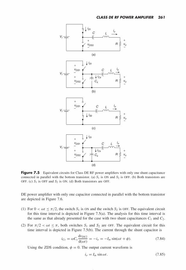
CLASS DE RF POWER AMPLIFIER 261
(a)
C LVI
+R vo
+vDS2
iS1
(c)
C LVI
+R vo
(b)
C LVI
+R vo
+vDS2
iCs
+vDS1
(d)
C LVI
+R vo
iS1
iCs
Cs
Cs
+vDS2
+vDS1
io
io
io
io
+vDS1
iS2
iS1
Figure 7.5 Equivalent circuits for Class DE RF power amplifiers with only one shunt capacitanceconnected in parallel with the bottom transistor. (a) S1 is ON and S2 is OFF. (b) Both transistors areOFF. (c) S1 is OFF and S2 is ON. (d) Both transistors are OFF.
DE power amplifier with only one capacitor connected in parallel with the bottom transistorare depicted in Figure 7.6.
(1) For 0 < ωt ≤ π/2, the switch S1 is ON and the switch S2 is OFF. The equivalent circuitfor this time interval is depicted in Figure 7.5(a). The analysis for this time interval isthe same as that already presented for the case with two shunt capacitances C1 and C2.
(2) For π/2 < ωt ≤ π , both switches S1 and S2 are OFF. The equivalent circuit for thistime interval is depicted in Figure 7.5(b). The current through the shunt capacitor is
iCs = ωCsdvDS 2
d(ωt)= −io = −Im sin(ωt + φ). (7.84)
Using the ZDS condition, φ = 0. The output current waveform is
io = Im sin ωt . (7.85)

262 RF POWER AMPLIFIERS
The current through the shunt capacitor is
iCs = −io = −Im sin ωt . (7.86)
ωt
0
0
vGS1
iS1
io
0
ωt
vGS2
Im
vDS1
ωt
ωt
ωt
0 π2
π 3π2
2π
iS2
iCs
0
vDS2
ωt
ωt
ωt0
0
2π
VI
VI
Figure 7.6 Voltage and current waveforms in Class DE RF power amplifiers with only one shuntcapacitance connected in parallel with the bottom transistor.
The drain-to-source voltage vDS 2 is given by
vDS 2 = 1
ωCs
∫ ωt
π2
iCs d(ωt) + VI = − Im
ωCs
∫ ωt
π2
sin ωt d(ωt) + VI = Im
ωCscos ωt + VI .
(7.87)
Imposing the ZVS condition, we obtainIm
ωCs= VI . (7.88)
Hence,
vDS 2 = VI (cos ωt + 1) (7.89)
and
vDS 1 = VI − vDS 2 = −VI cos ωt . (7.90)
(3) For π < ωt ≤ 3π/2, the switch S1 is OFF and the switch S2 is ON. The equivalentcircuit for this time interval is depicted in Figure 7.5(c). The analysis for this timeinterval is the same as that already presented for the case with two shunt capacitancesC1 and C2.

CLASS DE RF POWER AMPLIFIER 263
(4) For 3π/2 < ωt ≤ 2π , switches S1 and S2 are OFF. The equivalent circuit for this timeinterval is depicted in Figure 7.5(d). The current through the shunt capacitor is
iCs = ωCsdvDS 2
d(ωt)= −io = −Im sin(ωt + φ). (7.91)
The drain-to-source voltage vDS 2 is given by
vDS 2 = 1
ωCs
∫ ωt
π2
iCs d(ωt) = − Im
ωCs
∫ ωt
π2
sin ωt d(ωt) = Im
ωCscos ωt + VI . (7.92)
Imposing the ZVS condition, we obtain
Im
ωCs= VI . (7.93)
Hence,
vDS 2 = VI (cos ωt + 1) (7.94)
and
vDS 1 = VI − vDS 2 = −VI cos ωt . (7.95)
The dc input current is
II = 1
2π
∫ 2π
0iS 1d(ωt) = 1
2π
∫ π2
0Im sin ωt d(ωt) = Im
2π= ωCs
2πVI . (7.96)
The dc input resistance of the amplifier is
RI (DC ) = VI
II= 2π
ωCs. (7.97)
7.8 Components
The output power is
PO = V 2m
2R= V 2
I
2π2R(7.98)
Neglecting power losses, the efficiency is 100 %. The output power can be expressed as
PO = PI = II VI = ωCsV 2I
π. (7.99)
Hence,
ωCs R = 1
π. (7.100)
Thus,
Cs = 2C1 = 1
πωR. (7.101)
The single-shunt capacitance external to the transistors is given by
Cs(ext) = Cs − 2Co = 2C1(ext) (7.102)
where Co is the transistor output capacitance and Cs(ext) is the external shunt capacitance.In the Example 7.1, the two external shunt capacitances C1(ext) = 10 pF can be replaced bya single-shunt capacitance Cs(ext) = 2C1(ext) = 20 pF.

264 RF POWER AMPLIFIERS
7.9 Cancellation of Nonlinearities of TransistorOutput Capacitances
The transistor output capacitance Co is nonlinear. The output capacitance Co is large whenthe drain-to-source voltage vDS is low, and it is low when the drain-to-source voltage vDS
is high. The total voltage across both transistor output capacitances is constant
vDS 1 + vDS 2 = VI . (7.103)
In the Class DE amplifier, the transistor capacitances are connected in parallel for theac component [1]. When the voltage vDS 2 across the lower output capacitance Co2 islow, the capacitance Co2 is high. At the same time, the voltage vDS 1 is high and Co1 islow. Therefore, there is a partial cancellation of the nonlinearities of the total transistoroutput capacitance Cot = Co1 + Co2. The parallel combination of the shunt capacitance isapproximately constant. For this reason, the expressions for load network components andthe output power of the Class DE RF power amplifier are not affected by the nonlinearityof the transistor output capacitances [10, 11]. The shunt capacitances can be composedof only nonlinear transistor output capacitances or can be the combinations of nonlineartransistor output capacitances and linear external capacitances.
7.10 Summary
• The Class DE RF amplifier consists of two transistors, a series-resonant circuit, and shuntcapacitors.
• The transistors in the Class DE amplifier are operated as switches.
• There is a dead time in the gate-to-source voltages during which the drain-to-sourcevoltage of one transistor goes from high to low, and the drain-to-source voltage of theother transistor goes from low to high, and vice versa.
• The transistor output capacitances are absorbed into the shunt capacitances.
• Switching losses in the Class DE RF power amplifier are zero due to ZVS operation,like in the Class E amplifier.
• The voltage stress of power MOSFETs is low and equal to the supply voltage VI , likein the Class D amplifier.
• The nonlinearity of the transistor output capacitances does affect the values of the loadnetwork components and the output power.
• The Class DE power amplifier can be implemented with only one shunt capacitor andthe output capacitances of the transistors can be included in the circuit topology.
7.11 References
[1] M. K. Kazimierczuk and W. Szaraniec, ‘Class D zero-voltage switching inverter with onlyone shunt capacitor,’ IEE Proc., Part B, Electric Power Applications, vol. 139, pp. 449–456,September 1992.
[2] M. K. Kazimierczuk and D. Czarkowski, Resonant Power Converters, John Wiley & Sons,1995, ch. 10, pp. 295–308.

CLASS DE RF POWER AMPLIFIER 265
[3] H. Koizumi, T. Suetsugu, M. Fujii, K. Shinoda, S. Mori, and K. Iked, ‘Class DE high-efficiencytuned power amplifier,’ IEEE Trans. Circuits and Systems-I, Theory and Applications, vol. 43,no. 1, pp. 51–60, January 1996.
[4] K. Shinoda, T. Suetsugu, M. Matsuo, and S. Mori, ‘Idealized operation of the Class DE amplifiesand frequency multipliers,’ IEEE Trans. Circuits and Systems-I, Theory and Applications, vol.45, no. 1, pp. 34–40, January 1998.
[5] I. D. de Vries, J. H. van Nierop, and J. R. Greence, ‘Solid state Class DE RF power source,’Proc. of IEEE International Symposium on Industrial Electronics (ISIE’98), South Africa, July1998, pp. 524–529.
[6] S. Hintea and I. P. Mihu, ‘Class DE amplifiers and their medical applications,’ Proc of the 6-thInternational Conference on Optimization of Electric and Electronic Equipment (OPTIM’98),Romania, May 1998, pp. 697–702.
[7] M. Albulet, ‘An exact analysis of Class DE amplifier at any Q’, IEEE Trans. Circuits andSystems-I, Theory and Applications, vol. 46, no. 10, pp. 1228–1239, October 1999.
[8] T. Suetsugu and M. K. Kazimierczuk, ‘Integration of Class DE inverter for on-chip powersupplies,’ IEEE International Symposium on Circuits and Systems, May 2006, pp. 3133–3136.
[9] T. Suetsugu and M. K. Kazimierczuk, ‘Integration of Class DE dc-dc converter for on-chippower supplies,’ 37-th IEEE Power Electronics Specialists Conference (PESC’06), June 2006,pp. 1–5.
[10] H. Sekiya, T. Watanabe, T. Suetsugu, and M. K. Kazimierczuk, ‘Analysis and design of ClassDE amplifier with nonlinear shunt capacitances,’ The 7th IEEE International Conference onPower Electronics and Drive Systems (PEDS’07), Bangkok, Thailand, November 27–30, 2007.
[11] H. Sekiya, T. Watanabe, T. Suetsugu, and M. K. Kazimierczuk, ‘Analysis and design of ClassDE amplifier with nonlinear shunt capacitances,’ IEEE Transactions on Industry Applications,vol. 45, 2009.
7.12 Review Questions
7.1 How large are the switching losses in the Class DE RF power amplifier?
7.2 How large are the current and voltage stresses in the Class DE power amplifier?
7.3 How many transistors are used in the Class DE amplifier?
7.4 How are the transistors driven in the Class DE amplifier?
7.5 Can the Class DE power amplifier operate under ZVS condition?
7.6 Can the Class DE power amplifier operate under ZDS condition?
7.7 Is there any limitation for the operating frequency of the Class DE power amplifier?
7.8 How does the nonlinearity of the transistor output capacitances affect the values of theload network components and the output power of the Class DE power amplifier?
7.13 Problems
7.1 Design a Class DE amplifier to meet the following specifications: VI = 5 V, PO = 1 W,and f = 4 GHz. Assume that the output capacitances of the transistors are linear andequal to 1 pF.
7.2 Design a Class DE amplifier with a single shunt capacitance to meet the following spec-ifications: VI = 5 V, PO = 1 W, and f = 4 GHz. Assume that the output capacitancesof the transistors are linear and equal to 1 pF.


8Class F RF Power Amplifier
8.1 Introduction
Class F RF power amplifiers [1–24] utilize multiple-harmonic resonators in the outputnetwork to shape the drain-to-source voltage such that the transistor loss is reduced and theefficiency is increased. These circuits are also called polyharmonic or multi-resonant poweramplifiers. The drain current flows when the drain-to-source voltage is flat and low, andthe drain-to-source voltage is high when the drain current is zero. Therefore, the productof the drain current and the drain-to-source voltage is low, reducing the power dissipationin the transistor. This method of improving the efficiency is the oldest technique and wasinvented by Tyler in 1919 [1]. Class F power amplifiers with lumped-element resonantcircuits tuned to the third harmonic or to the third and fifth harmonics have been widelyused in high-power amplitude-modulated (AM) broadcast radio transmitters in the LF range(30–300 kHz), the MF range (0.3–3 MHz), and the HF range (3–30 MHz). Class F poweramplifiers with a quarter-wavelength transmission line controls all the odd harmonics andare used in VHF (30–300 MHz) frequency-modulated (FM) broadcast radio transmitters[1]. They are also used in UHF (300 MHz to 3 GHz) FM broadcast radio transmitters [2].Dielectric resonators can be used in place of lumped-element resonant circuits. Outputpower of 40 W has been achieved at 11 GHz with an efficiency of 77 %. In this chapter, wewill present Class F power amplifier circuits, principle of operation, analysis, and designexample.
There are two groups of Class F RF power amplifiers:
• odd harmonic Class F power amplifiers;
• even harmonic Class F power amplifiers.
In Class F amplifiers with odd harmonics, the drain-to-source voltage contains only odd har-monics and the drain current contains only even harmonics. Therefore, the input impedanceof the load network represents an open circuit at odd harmonics and a short circuit at evenharmonics. The drain-to-source voltage vDS of Class F amplifiers with odd harmonics is
RF Power Amplifiers Marian K. Kazimierczuk 2008 John Wiley & Sons, Ltd

268 RF POWER AMPLIFIERS
symmetrical for the lower and upper half of the cycle. In general, the drain-to-source voltagevDS of Class F amplifiers with odd harmonics is given by
vDS = VI − Vm cos ωot +∞∑
n=3,5,7,...
Vmn cos nωot (8.1)
and the drain current is
iD = II + Im cos ωot +∞∑
n=2,4,6,...
Imn cos nωot . (8.2)
In Class F amplifiers with even harmonics, the drain-to-source voltage contains only evenharmonics and the drain current contains only odd harmonics. Hence, the load networkrepresents an open circuit at even harmonics and a short circuit at odd harmonics. Theinput impedance of the load network at each harmonic frequency is either zero or infinity.The drain-to-source voltage vDS of Class F amplifiers is not symmetrical for the lower andupper half of the cycle.
The drain-to-source voltage vDS of Class F amplifiers with even harmonics is given by
vDS = VI − Vm cos ωot +∞∑
n=2,4,6,...
Vmn cos nωot (8.3)
and the drain current is
iD = II + Im cos ωot +∞∑
n=3,5,7,...
Imn cos nωot . (8.4)
No real power is generated at harmonics because there is either no current or no voltagepresent at each harmonic frequency. There are finite and infinite order Class F poweramplifiers.
Two particular categories of high-efficiency Class F power amplifiers can be distin-guished:
• Class F power amplifiers with maximally flat drain-to-source voltage;
• Class F power amplifiers with maximum drain efficiency.
For Class F amplifiers with symmetrical drain-to-source voltage vDS , the maximally flatvoltage occurs at two values of ωot , at the bottom part of the waveform and the toppart of the waveform. For Class F amplifiers with unsymmetrical drain-to-source voltagevDS , the maximally flat voltage occurs only at one value of ωot at the bottom part of thewaveform. All the derivatives of voltage vDS are zero at ω0t at which the voltage vDS ismaximally flat.
8.2 Class F RF Power Amplifier with Third Harmonic
The circuit of the Class F RF power amplifier with a third harmonic resonator [1] is shownin Figure 8.1. This circuit is called the Class F3 power amplifier. It consists of a transistor,load network, and RF choke (RFC). The load network consists of a parallel-resonant LCcircuit tuned to the operating frequency fo and a parallel-resonant circuit tuned to the thirdharmonic 3fo . The two resonant circuits are connected in series. The ac power is deliveredto the load resistance R.

CLASS F RF POWER AMPLIFIER 269
(b)
R vo
+vDS
+
VI
L3
C3
L C
RFC
CB
II
iD
io
fo
3fo
(a)
R vo
+vDS
+
VI
L3
foC3
L C
RFC
CB
~ vGS
+
II
iD
io
3fo
Figure 8.1 Class F3 power amplifier with a third harmonic resonator. (a) Circuit. (b) Equivalentcircuit.
Figure 8.2 shows the voltage and current waveforms of the Class F power amplifier witha third harmonic. The drain current waveform may have any conduction angle 2θ < 2π ,which contains higher harmonics. In most applications, the conduction angle is θ = π , likein the Class B amplifier. In this case, the drain current is a half-sine wave given by
iD =
IDM cos ωot for −π
2< ωot ≤ π
2
0 forπ
2< ωot ≤ 3π
2.
(8.5)
where IDM is the peak value of the drain current, which occurs at ωt = 0. Other values ofthe conduction angle θ are also possible.
The output resonant circuit tuned to the fundamental frequency fo acts like a band-passfilter and filters out all the harmonics of the drain current. Therefore, the output voltagewaveform is sinusoidal
vo = −Vm cos ωot . (8.6)
The fundamental component of the drain-to-source voltage is
vds1 = vo = −Vm cos ωot . (8.7)
The voltage across the parallel-resonant circuit tuned to the third harmonic 3fo is
vds3 = Vm3 cos 3ωot . (8.8)
The third harmonic voltage waveform is 180 out of phase with respect to the fundamentalfrequency voltage vds1. The voltages at all other harmonic frequencies are zero. The drain-to-source voltage waveform is given by
vDS = VI + vds1 + vds3 = VI − Vm cos ωot + Vm3 cos 3ωot . (8.9)

270 RF POWER AMPLIFIERS
ωt0
IDM
iD
23π
2π
ωt0
vDS
VI
23π
2π
2π
ωt02
vGS
3π2π
2π
ωt02
vo
3π2π
2π
2π
0
pD
2π
2π
23π ωt
Vm
Figure 8.2 Waveforms in Class F RF power amplifier with a third harmonic peaking.
The third harmonic flattens the drain-to-source voltage vDS so that the drain current iD flowswhen the drain-to-source voltage vDS is low, as shown in Figure 8.2. When the drain-to-source voltage vDS is high, the drain current is zero. Therefore, the average value of thedrain voltage-current product is reduced. This results in both high drain efficiency ηD andhigh output-power capability cp .
When the third harmonic is added to the fundamental component, the peak-to-peak swing2Vpk of the ac component of the composed drain-to-source voltage waveform is reduced,

CLASS F RF POWER AMPLIFIER 271
and the peak value of the resulting ac component of the drain-to-source voltage Vpk is lowerthan the amplitude of the fundamental component Vm . The waveform of vDS changes asthe ratio Vm3/Vm increases.
(1) For 0 < Vm3/Vm < 1/9, the resulting waveform of vDS has a single valley at ωot = 0and a single peak at ωt = π . In other words, the minimum value of vDS occurs atωot = 0 and the maximum value of vDS occurs at ωot = π . The peak value of the accomponent of vDS is
Vpk = VI − VDSmin = VI − vDS (0) = VI − VI + Vm − Vm3 = Vm − Vm3. (8.10)
For an ideal transistor, VDSmin = 0 and Vpk = VI . Hence,
Vm
Vpk= Vm
VI= Vm
Vm − Vm3= 1
1 − Vm3
Vm
. (8.11)
As Vm3/Vm increases, Vm/VI also increases.
(2) At Vm3/Vm = 1/9, the waveform of vDS is maximally flat. The minimum value of vDS
occurs at ωot = 0 and the maximum value of vDS occurs at ωot = π .
(3) For Vm3/Vm > 1/9, the waveform of vDS exhibits a ripple with double peaks, as shownin Figure 8.2. There is a local maximum value of vDS at ωot = 0 and two local adjacentminimum values. In addition, there is a local minimum value of vDS at ωot = π andtwo local adjacent maximum values.
(4) As Vm3/Vm increases from 1/9, the ratio Vm/VI reaches its maximum value at Vm3/
Vm = 1/6 and is given by
Vm
Vpk= Vm
VI= 2√
3. (8.12)
(5) For Vm3/Vm > 1/6, the waveform of vDS has double valleys and a peak at low voltagesand double peaks and one valley at high voltages. The ratio Vm/Vpk decreases asVm3/Vm increases.
It is possible to increase the ratio Vm/VI by adding a small amount of third harmonic,while maintaining vDS ≥ 0. When VI and II are held constant, PI is constant. As Vm
increases, PO = Vm Im/2 increases, and therefore ηD = PO/PI also increases by the samefactor by which Vm is increased.
8.2.1 Maximally Flat Class F3 Amplifier
In order to find the maximally flat waveform of vDS , we determine its derivative and setthe result to be equal to zero
dvDS
d(ωot)= Vm sin ωot − 3Vm3 sin 3ωot = Vm sin ωot − 3Vm3(3 sin ωot − 4 sin3 ωot)
= sin ωot(Vm − 9Vm3 + 12Vm3 sin2 ωot) = 0. (8.13)
One solution of this equation at non-zero values of Vm and Vm3 is
sin ωotm = 0 (8.14)

272 RF POWER AMPLIFIERS
which gives the location of one extremum (a minimum or a maximum) of vDS at
ωotm = 0 (8.15)
and the other extremum of vDS at
ωotm = π. (8.16)
The other solutions are
sin ωotm = ±√
9Vm3 − Vm
12Vm3for Vm3 ≥ Vm
9. (8.17)
The real solutions of this equation do not exist for Vm3 < Vm/9. For ωot > Vm/9, thereare two minimum values of vDS at
ωotm = ± arcsin
√9Vm3 − Vm
12Vm3(8.18)
and two maximum values of vDS at
ωotm = π ± arcsin
√9Vm3 − Vm
12Vm3. (8.19)
ForVm3
Vm= 1
9(8.20)
the location of three extrema of vDS converges to 0 and the location of the other threeextrema converges to π . In this case, the waveform of vDS is maximally flat at ωot = 0and at ωot = π .
For the symmetrical and maximally flat drain-to-source voltage vDS , the minimum valueof vDS occurs at ωot = 0 and the maximum value occurs at ωot = π . The Fourier coeffi-cients for the maximally flat waveform of vDS can be derived by setting all the derivativesof vDS to zero. The first and the second-order derivatives of voltage vDS are
dvDS
d(ωot)= Vm sin ωot − 3Vm3 sin 3ωot (8.21)
andd2vDS
d(ωot)2= Vm cos ωot − 9Vm3 cos 3ωot . (8.22)
The first-order derivative is zero at ωot = 0 and ωot = π , but it does not generate anequation because sin 0 = sin π = 0. From the second-order derivative of vDS at ωot = 0,
d2vDS
d(ωot)2
∣∣∣∣ωo t=0
= Vm − 9Vm3 = 0. (8.23)
Thus, a maximally flat waveform of the drain-to-source voltage occurs for
Vm3
Vm= 1
9. (8.24)
Idealy, the minimum drain-to-source voltage is
VDSmin = vDS (0) = VI − Vm + Vm3 = VI − Vm + Vm
9= VI − 8
9Vm = 0 (8.25)
producing the maximum amplitude of the output voltage
Vm = 9
8VI . (8.26)

CLASS F RF POWER AMPLIFIER 273
−90 −60 −30 0 30 60 90 120 150 180 210 240 2700
0.2
0.4
0.6
0.8
1
1.2
1.4
1.6
1.8
2
ωo t (°)
v DS /
VI
n = 1, 3
Figure 8.3 Maximally flat waveform of the normalized drain-to-source voltage vDS /VI for ClassF RF power amplifier with third harmonic peaking.
Similarly,
VDSmin = vDS (0) = VI − Vm + Vm3 = VI − 9Vm3 + Vm3 = VI − 8Vm3 = 0 (8.27)
yielding the amplitude of the third harmonic voltage
Vm3 = VI
8. (8.28)
The maximum drain-to-source voltage is
VDSM = vDS (π ) = VI + Vm − Vm3 = VI + 9
8VI − 1
8VI = 2VI . (8.29)
The normalized maximally flat waveform of vDS is
vDS
VI= 1 − Vm
VIcos ωot + Vm3
VIcos 3ωot = 1 − 9
8cos ωot + 1
8cos 3ωot . (8.30)
Figure 8.3 shows the maximally flat waveform of the normalized drain-to-source voltagevDS /VI with the third harmonic peaking.
The fundamental component of the load current is equal to the drain current
io = id1 = Im cos ωot (8.31)
where
Im = 1
π
∫ π2
− π2
iD cos ωot d(ωot) = 1
π
∫ π2
− π2
IDM cos2 ωot d(ωot) = IDM
2(8.32)
or
Im = Vm
R= 9(VI − VDSmin )
8R. (8.33)

274 RF POWER AMPLIFIERS
The dc input current is equal to the component of the drain current
II = 1
2π
∫ π2
− π2
iD d(ωo t) = 1
2π
∫ π2
− π2
IDM cos ωot d(ωot) = IDM
π= 2
πIm = 9(VI − VDSmin )
4πR.
(8.34)The dc input power is given by
PI = VI II = 9VI (VI − VDSmin )
4πR= 9VI (VI − VDSmin )
4πR. (8.35)
The drain current iD contains the dc component, fundamental component, and even harmon-ics. The drain-to-source voltage vDS contains the dc component, fundamental component,and third harmonic. Therefore, the output power contains only the fundamental component
PO = 1
2Im Vm = 1
2× IDM
2× 9
8(VI − VDSmin ) = 9
32IDM (VI − VDSmin ) (8.36)
or
PO = V 2m
2R= 81(VI − VDSmin )2
128R= 0.6328
(VI − VDSmin )2
R. (8.37)
Hence, the drain efficiency of the amplifier is
ηD = PO
PI= 1
2
(Im
II
)(Vm
VI
)= 1
2× π
2×(
Vm
VI
)= π
4
Vm
VI= π
4× 9
8
(1 − VDSmin
VI
)
= 9π
32
(1 − VDSmin
VI
)= 0.8836
(1 − VDSmin
VI
). (8.38)
The ratio of the drain efficiency ηD(F3) for the Class F amplifier with the third harmonic tothe efficiency of Class B amplifier at VDSmin = 0 is
ηD(F3)
ηD(B )= 9
8= 1.125. (8.39)
Thus, the improvement in the efficiency of the Class F amplifier over that of the ClassB amplifier is by a factor of 1.125 from 78.54 % to 88.36 %. Note that the amplitude ofthe fundamental component Vm = VI is increased in the Class F amplifier with the thirdharmonic to Vm = 9VI /8 = 1.125VI . Thus, the drain efficiency ηD and the ratio Vm/VI areincreased by the same factor, equal to 1.125.
The output-power capability is
cp = PO
VDSM IDM= PO
2VI IDM= 9
64
(1 − VDSmin
VI
)= 0.1406
(1 − VDSmin
VI
)(8.40)
where the maximum value of the drain-to-source voltage is VDSM = 2VI . The dc inputresistance is
RDC = VI
II= 4π
9R ≈ 1.396R. (8.41)
Example 8.1
Design a Class F power amplifier employing third harmonic peaking with a maximallyflat drain-to-source voltage to deliver a power of 10 W at fc = 800 MHz. The requiredbandwidth is BW = 100 MHz. The dc power supply voltage is 12 V and VDSmin = 1 V.

CLASS F RF POWER AMPLIFIER 275
Solution. The maximum amplitude of the fundamental component of the drain-to-sourcevoltage is
Vm = 9
8(VI − VDSmin ) = 9
8(12 − 1) = 12.375 V. (8.42)
The amplitude of the third harmonic is
Vm3 = Vm
9= 12.375
9= 1.375 V. (8.43)
The load resistance is
R = V 2m
2PO= 12.3752
2 × 10= 7.657 . (8.44)
The maximum drain-to-source voltage is
VDSmax = 2VI = 2 × 12 = 24 V. (8.45)
The amplitude of the fundamental component of the drain current is
Im = Vm
R= 12.375
7.657= 1.616 A. (8.46)
The maximum drain current is
IDM = 2Im = 2 × 1.616 = 3.232 A. (8.47)
The dc supply current is
II = IDM
π= 3.232
π= 1.029 A. (8.48)
The dc supply power is
PI = II VI = 1.029 × 12 = 12.348 W. (8.49)
The drain power loss of the transistor is
PD = PI − PO = 12.348 − 10 = 2.348 W. (8.50)
The drain efficiency is
ηD = PO
PI= 10
12.348= 80.98 %. (8.51)
The dc resistance presented by the amplifier to the dc source is
RDC = 4π
9R = 1.396 × 7.657 = 10.689 . (8.52)
The loaded quality factor is
QL = fcBW
= 800
100= 8. (8.53)
The definition of the loaded quality factor for a parallel-resonant circuit is
QL = R
ωcL= ωcCR. (8.54)
The inductance of the resonant circuit tunned the fundamental is
L = R
ωcQL= 7.657
2π × 0.8 × 109 × 8= 0.19 nH. (8.55)
The capacitance‘ of the resonant circuit tunned the fundamental is
C = QL
ωcR= 8
2π × 0.8 × 109 × 7.657= 207.855 pF. (8.56)

276 RF POWER AMPLIFIERS
8.2.2 Maximum Drain Efficiency Class F3 Amplifier
The maximum drain efficiency ηD and the maximum output-power capability cp do notoccur for the maximally flat drain-to-source voltage vDS , but when the waveform vDS
exhibits slight ripple. From (8.17),
cos ωotm =√
1 − sin2 ωotm =√
1 − 9Vm3 − Vm
12Vm3=√
1
4+ Vm
12Vm3. (8.57)
The minimum value of vDS occurs at ωotm and is equal to zero
vDS (ωotm ) = VI − Vm cos ωotm + Vm3 cos 3ωotm = 0 (8.58)
which gives
VI = Vm cos ωotm − Vm3 cos 3ωotm = Vm cos ωotm − Vm3(4 cos3 ωotm − 3 cos ωotm )
= cos ωotm (Vm − 4Vm3 cos2 ωotm + 3Vm3) =√
1
4+ Vm
12Vm3
(2Vm
3+ 2Vm3
)
= Vm
[(2
3+ 2Vm3
Vm
)√1
4+ Vm
12Vm3
](8.59)
Hence,Vm
VI= 1√
1
4+ Vm
12Vm3
(2
3+ 2Vm3
Vm
) . (8.60)
In order to maximize the drain efficiency
ηD = PO
PI= 1
2
(Im
II
)(Vm
VI
)(8.61)
at a given waveform of drain current iD , i.e., at a given ratio Im/II , we will maximize theratio Vm/VI . As Vm3 increases when Vm is held constant, VI first decreases, reaches itsminimum value, and then slowly increases. To maximize Vm/VI , we take the derivativeand set it to zero
d
(Vm
VI
)
d
(Vm3
Vm
) = 9(9 + 3Vm
Vm3
) 23
12
3+ 2Vm3
Vm
(Vm
Vm3
)2
− 12√9 + 3Vm
Vm3
1(2
3+ 2Vm3
Vm
)2 = 0
(8.62)producing
18
(Vm3
Vm
)2
+ 3
(Vm3
Vm
)− 1 = 0. (8.63)
Solution of this equation yieldsVm3
Vm= 1
6≈ 0.1667. (8.64)
Using this relationship, we obtain
VI = Vm cos ωotm − Vm3 cos 3ωotm = Vm cos ωotm − Vm3(4 cos3 ωotm − 3 cos ωotm )
= Vm
√1
4+ 1
2
[1 − 2
3
(1 + 2
4
)+ 1
2
]= Vm
√3
2(8.65)

CLASS F RF POWER AMPLIFIER 277
resulting inVm
VI= 2√
3≈ 1.1547. (8.66)
Finally,
Vm3 = Vm
6= VI
3√
3(8.67)
yieldingVm3
VI= 1
3√
3≈ 0.19245. (8.68)
The minimum values of vDS occur at
ωotm = ± arcsin
√9Vm3 − Vm
12Vm3= ± arcsin
(1
2
)= ±30
. (8.69)
The normalized waveform vDS /VI for achieving the maximum drain efficiency is given byvDS
VI= 1 − Vm
VIcos ωot + Vm3
VIcos 3ωot = 1 − 2√
3cos ωot + 1
3√
3cos 3ωot . (8.70)
The normalized drain-to-source voltage waveform vDS /VI for the Class F amplifier withthe third harmonic peaking for the maximum drain efficiency is shown in Figure 8.4. Thedrain efficiency is
ηD = PO
PI= 1
2
Im
II
Vm
VI= 1
2× π
2× 2√
3= π
2√
3≈ 90.67 %. (8.71)
−90 −45 0 45 90 135 180 225 2700
0.2
0.4
0.6
0.8
1
1.2
1.4
1.6
1.8
2
ωot (°)
v DS /V
I
Figure 8.4 Waveform of the normalized drain-to-source voltage vDS /VI for Class F RF poweramplifier with third harmonic peaking, yielding the maximum drain efficiency and output-powercapability.

278 RF POWER AMPLIFIERS
The ratio of the maximum drain efficiency ηDmax (F3) of the Class F amplifier with the thirdharmonic to the drain efficiency of the Class B amplifier at VDSmin = 0 is
ηDmax (F3)
ηD(B )= 2√
3≈ 1.1547. (8.72)
Thus, the maximum drain efficiency is increased from 78.54 % to 90.67 % by the samefactor as the ratio Vm/VI is increased, i.e., by a factor of 2/
√3 ≈ 1.1547.
In general, the drain efficiency of the Class F amplifier is given by
ηD = ηB
(Vm
VI
)= π
4
(Vm
VI
). (8.73)
Hence,
ηD = π
4
1
1 − Vm3
Vm
for 0 ≤ Vm3
Vm≤ 1
9. (8.74)
and
ηD = π
4
√1
4+ Vm
12Vm3
(2
3+ 2Vm3
Vm
) forVm3
Vm≥ 1
9. (8.75)
Figure 8.5 shows Vm/VI as a function of Vm3/Vm . The drain efficiency ηD as a functionof Vm3/Vm is shown in Figure 8.6.
The ratio of the maximum drain efficiency ηDmax (F3) of the Class F amplifier with thethird harmonic to the drain efficiency of the Class B amplifier with maximally flat waveform
0 0.05 0.1 0.15 0.2 0.25 0.3 0.35 0.41
1.02
1.04
1.06
1.08
1.1
1.12
1.14
1.16
Vm3/Vm
Vm
/VI
Figure 8.5 Ratio Vm/VI as a function of Vm3/Vm for Class F RF power amplifier with thirdharmonic peaking.

CLASS F RF POWER AMPLIFIER 279
0 0.05 0.1 0.15 0.2 0.25 0.3 0.35 0.478
80
82
84
86
88
90
92
Vm3 /Vm
η D (
%)
Figure 8.6 Drain efficiency ηD as a function of Vm3/Vm for Class F RF power amplifier withthird harmonic peaking.
vDS at VDSmin = 0 is
ηDmax (F3)
ηD(F3)= 16
9√
3≈ 1.0264. (8.76)
Thus, the improvement in the efficiency is by 2.64 %. The maximum drain-to-source volt-age is
VDSM = 2VI . (8.77)
The maximum output-power capability is
cp = PO
IDM VDSM= ηD PI
IDM VDSM= ηD
II VI
IDM VDSM=(
π
2√
3
)(1
π
)(1
2
)= 1
4√
3≈ 0.1443.
(8.78)The maximum output-power capability at any value of Vm3/Vm is given by
cp = 1
2
(Im
IDM
)(Vm
VDSM
)= 1
2
(Im
IDM
)(Vm
2VI
)= 1
8
(Vm
VI
)= cp(B )
(Vm
VI
). (8.79)
Thus,
cp = 1
8
1
1 − Vm3
Vm
for 0 ≤ Vm3
Vm≤ 1
9. (8.80)
and
cp = 1
8
√1
4+ Vm
12Vm3
(2
3+ 2Vm3
Vm
) forVm3
Vm≥ 1
9. (8.81)

280 RF POWER AMPLIFIERS
0 0.05 0.1 0.15 0.2 0.25 0.3 0.35 0.40.125
0.13
0.135
0.14
0.145
Vm3/Vm
c p
Figure 8.7 Output power capability cp as a function of Vm3/Vm for Class F RF power amplifierwith third harmonic peaking.
Figure 8.7 shows cp as a function of Vm3/Vm . For odd harmonic Class F amplifiers, themaximum drain efficiency and the maximum output power capability occur at the samevoltage amplitude ratios.
The dc resistance of the amplifier presented to the dc power supply is
RDC = VI
II= π
√3
2R ≈ 1.36 R. (8.82)
Example 8.2
Design a Class F power amplifier employing third harmonic peaking and having a maximumdrain efficiency to deliver a power of 10 W at fc = 800 MHz with BW = 100 MHz. The dcpower supply voltage is 12 V and VDSmin = 1 V.
Solution. The maximum amplitude of the fundamental component of the drain-to-sourcevoltage is
Vm = 2√3
(VI − VDSmin ) = 1.1547(12 − 1) = 12.7 V. (8.83)
The amplitude of the third harmonic is
Vm3 = Vm
6= 12.7
6= 2.117 V. (8.84)
The load resistance is
R = V 2m
2PO= 12.72
2 × 10= 8.0645 . (8.85)

CLASS F RF POWER AMPLIFIER 281
The maximum drain-to-source voltage is
VDSmax = 2VI = 2 × 12 = 24 V. (8.86)
The amplitude of the fundamental component of the drain current is
Im = Vm
R= 12.7
8.0645= 1.575 A. (8.87)
The maximum drain current is
IDM = 2Im = 2 × 1.575 = 3.15 A. (8.88)
The dc supply current is
II = IDM
π= 3.15
π= 1.00267 A. (8.89)
The dc supply power is
PI = II VI = 1.00267 × 12 = 12.03204 W. (8.90)
The drain power loss of the transistor is
PD = PI − PO = 12.03204 − 10 = 2.03204 W. (8.91)
The drain efficiency is
ηD = PO
PI= 10
12.03204= 83.11 %. (8.92)
The dc resistance presented by the amplifier to the dc power supply is
RDC = π√
3
4R ≈ 1.36 × 8.0645 = 10.97 . (8.93)
From Example 8.1, L = 0.19 nH and C = 207.855 pF.The loaded quality factor of the resonant circuit tunned to the fundamental of the carrier
frequency is
QL = fcBW
= 800
100= 8. (8.94)
The resonant circuit components of the output circuit are
L = R
ωcQL= 8.0645
2π × 0.8 × 109 × 8= 0.2 nH (8.95)
and
C = QL
ωcR= 8
2π × 0.8 × 109 × 8.0645= 197.35 pF. (8.96)
8.3 Class F RF Power Amplifier with Third and FifthHarmonics
8.3.1 Maximally Flat Class F35 Amplifier
The circuit of a Class F RF power amplifier with both the third and fifth harmonics isdepicted in Figure 8.8. This circuit is called the Class F35 amplifier. The voltage and

282 RF POWER AMPLIFIERS
(b)
R vo
+vDS
+
VI
L3
C3
L C
RFC
CB
II
iD
io
fo
3fo
(a)
R vo
+vDS
+
VI
L3
foC3
L C
RFC
CB
~ vGS
+
II
iD
io
3foL5
C5
5fo
L5
C5
5fo
Figure 8.8 Class F power amplifier with third and fifth harmonic resonators. (a) Circuit.(b) Equivalent circuit.
current waveforms are shown in Figure 8.9. The drain-to-source voltage waveform is
vDS = VI − Vm cos ωot + Vm3 cos 3ωot − Vm5 cos 5ωot . (8.97)
The derivatives of this voltage are
dvDS
d(ωot)= Vm sin ωot − 3Vm3 sin 3ωot + 5Vm5 sin 5ωot (8.98)
d2vDS
d(ωot)2= Vm cos ωot − 9Vm3 cos 3ωot + 25Vm5 cos 5ωot (8.99)
d3vDS
d(ωot)3= −Vm sin ωot + 27Vm3 sin 3ωot − 125Vm5 sin 5ωot (8.100)
and
d4vDS
d(ωot)4= −Vm cos ωot + 81Vm3 cos 3ωot − 625Vm5 cos 5ωot . (8.101)
All the terms of the first and third-order derivatives are zero at ωot = 0 and do not giveany equations. The second and the fourth-order derivatives are zero at ωot = 0, yielding aset of two simultaneous equations
d2vDS
d(ωot)2
∣∣ωo t=0 = Vm − 9Vm3 + 25Vm5 = 0 (8.102)
and
d4vDS
d(ωot)4
∣∣ωo t=0 = −Vm + 81Vm3 − 625Vm5 = 0. (8.103)

CLASS F RF POWER AMPLIFIER 283
ωt0
IDM
iD
23π
2π
ωt0
vDS
VI
23π
2π
2π
ωt02
vGS
3π2π
2π
ωt0
vo
Vm
2π
0
pD
23π
2π
2π
23π
2π
2π ωt
Figure 8.9 Waveforms in Class F RF power amplifier with third and fifth harmonic peaking.
Solution of this set of equations gives
Vm3 = Vm
6(8.104)
Vm5 = Vm
50(8.105)
andVm5 = 3
25Vm3. (8.106)

284 RF POWER AMPLIFIERS
Now
vDS (0) = VI − Vm + Vm3 − Vm5 = VI − Vm + Vm
6− Vm
50= VI − 64
75Vm = 0 (8.107)
producing
Vm = 75
64VI ≈ 1.1719VI . (8.108)
Similarly,
vDS (0) = VI − Vm + Vm3 − Vm5 = VI − 6Vm3 + Vm3 − 3Vm3
25= VI − 128
25Vm3 = 0
(8.109)yielding
Vm3 = 25
128VI ≈ 0.1953VI . (8.110)
Finally,
vDS (0) = VI − Vm + Vm3 − Vm5 = VI − 50Vm5 + 25
3Vm5 − Vm5 = VI − 128
3Vm5 = 0
(8.111)leading to
Vm5 = 3
128VI ≈ 0.02344VI . (8.112)
The maximum drain-to-source voltage is
VDSM = vDS (π ) = VI + Vm − Vm3 + Vm5 = VI + 75
64VI − 25
128VI + 3
128VI = 2VI .
(8.113)The normalized maximally flat voltage is given by
vDS
VI= 1 − Vm
VIcos ωot + Vm3
Vmcos 3ωot − Vm5
Vmcos 5ωot
= 1 − 75
64cos ωot + 25
128cos 3ωot − 3
128cos 5ωot . (8.114)
Figure 8.10 shows the maximally flat waveform of the normalized drain-to-source voltagevDS /VI with the third and fifth harmonics.
The amplitude of the fundamental component of the current is
Im = Vm
R= 75
64
VI
R. (8.115)
The dc input current is
II = 2
πIm = 75
32π
VI
R. (8.116)
The dc input power is
PI = II VI = 75
32π
V 2I
R. (8.117)
The output power is
PO = V 2m
2R= 5625
8192
V 2I
R≈ 0.6866
V 2I
R. (8.118)

CLASS F RF POWER AMPLIFIER 285
−90 −60 −30 0 30 60 90 120 150 180 210 240 2700
0.2
0.4
0.6
0.8
1
1.2
1.4
1.6
1.8
2
ωot (°)
v DS /
VI
n = 1, 3, 5
Figure 8.10 Maximally flat waveform of the normalized drain-to-source voltage vDS /VI for ClassF RF power amplifier with third and fifth harmonics.
The drain efficiency is
ηD = PO
PI= 75π
256≈ 92.04 % (8.119)
The maximum drain-to-source voltage is
VDSM = 2VI . (8.120)
The output-power capability is
cp = PO
VDSM IDM= 1
2
(Vm Im
2VI IDM
)= 1
4× 75
64× 1
2= 75
512= 0.1465. (8.121)
The dc input resistance is
RDC = VI
II= 32π
75R ≈ 1.34R. (8.122)
Example 8.3
Design a Class F power amplifier employing third and fifth harmonics peaking with amaximally flat drain-to-source voltage to deliver a power of 16 W at fc = 1 GHz. Therequired bandwidth is BW = 100 MHz. The dc power supply voltage is 24 V and VDSmin =1 V.
Solution. The maximum amplitude of the fundamental component of the drain-to-sourcevoltage is
Vm = 75
64(VI − VDSmin ) = 75
64(24 − 1) = 26.953 V. (8.123)

286 RF POWER AMPLIFIERS
The amplitude of the third harmonic is
Vm3 = Vm
6= 26.953
6= 4.492 V. (8.124)
Vm5 = Vm
50= 26.953
50= 0.5391 V. (8.125)
The load resistance is
R = V 2m
2PO= 26.9532
2 × 16= 22.7 . (8.126)
The maximum drain-to-source voltage is
VDSmax = 2VI = 2 × 24 = 48 V. (8.127)
The amplitude of the fundamental component of the drain current is
Im = Vm
R= 26.953
22.7= 1.187 A. (8.128)
The maximum drain current is
IDM = 2Im = 2 × 1.187 = 2.374 A. (8.129)
The dc supply current is
II = IDM
π= 2.374
π= 0.7556 A. (8.130)
The dc supply power is
PI = II VI = 0.7556 × 24 = 18.1344 W. (8.131)
The drain power loss of the transistor is
PD = PI − PO = 18.1344 − 16 = 2.1344 W. (8.132)
The drain efficiency is
ηD = PO
PI= 16
18.1344= 88.23 %. (8.133)
The dc resistance presented by the amplifier to the dc source is
RDC = 32π
75R = 1.34 × 22.7 = 30.418 . (8.134)
The loaded quality factor is
QL = fcBW
= 1000
100= 10. (8.135)
The inductance of the resonant circuit tunned the fundamental frequency is
L = R
ωcQL= 22.7
2π × 109 × 10= 0.36128 nH. (8.136)
The capacitance of the resonant circuit tunned the fundamental frequency is
C = QL
ωcR= 10
2π × 109 × 22.7= 70.11 pF. (8.137)

CLASS F RF POWER AMPLIFIER 287
8.3.2 Maximum Drain Efficiency Class F35 Amplifier
The maximum drain efficiency and the output-power capability of the Class F amplifierwith the third and fifth harmonics is obtained for [20]
Vm
VI= 1.2071 (8.138)
Vm3
VI= 0.2804 (8.139)
Vm5
VI= 0.07326 (8.140)
Vm3
Vm= 0.2323 (8.141)
Vm5
Vm= 0.0607 (8.142)
andVm5
Vm3= 0.2613. (8.143)
The normalized waveform vDS /VI for the maximum drain efficiency is given by
vDS
VI= 1 − Vm
VIcos ωot + Vm3
Vmcos ωot + Vm5
VIcos 5ωot
= 1 − 1.2071 cos ωot + 0.2804Vm cos ωot + 0.07326 cos 5ωot . (8.144)
The waveform of normalized drain-to-source voltage vDS /VI in the Class F amplifier withthe third and fifth harmonics, yielding the maximum drain efficiency and the maximumoutput-power capability, is shown in Figure 8.11.
The amplitude of the fundamental component of the drain current is
Im = Vm
R= 1.207VI
R. (8.145)
The dc supply current is
II = 2
πIm = 2 × 1.207
π
VI
R= 0.7684
VI
R. (8.146)
The dc supply current is
PI = II VI = 0.7684V 2
I
R. (8.147)
The output power is
PO = V 2m
2R= 1
2
(1.207VI )2
R≈ 0.7284
V 2I
R. (8.148)
The maximum drain efficiency is
ηD = PO
PI= 1
2
(Im
II
)(Vm
VI
)= 1
2
(π
2
)(1.207) = π
4× 1.207 ≈ 94.8 %. (8.149)
Hence,ηDmax
ηD(F35)= 94.8
92.4= 1.026. (8.150)
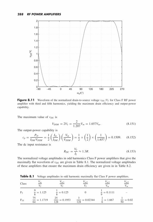
288 RF POWER AMPLIFIERS
−90 −45 0 45 90 135 180 225 2700
0.2
0.4
0.6
0.8
1
1.2
1.4
1.6
1.8
2
ωot (°)
v DS
/VI
Figure 8.11 Waveform of the normalized drain-to-source voltage vDS /VI for Class F RF poweramplifier with third and fifth harmonics, yielding the maximum drain efficiency and output-powercapability.
The maximum value of vDS is
VDSM = 2VI = 2
1.207Vm = 1.657Vm . (8.151)
The output-power capability is
cp = PO
IDM VDSM= 1
2
(Im
IDM
)(Vm
VDSM
)= 1
2×(
1
2
)×(
1
1.657
)= 0.1509. (8.152)
The dc input resistance is
RDC = VI
II≈ 1.3R. (8.153)
The normalized voltage amplitudes in odd harmonics Class F power amplifiers that give themaximally flat waveform of vDS are given in Table 8.1. The normalized voltage amplitudesof these amplifiers that ensure the maximum drain efficiency are given in in Table 8.2.
Table 8.1 Voltage amplitudes in odd harmonic maximally flat Class F power amplifiers.
ClassVm
VI
Vm3
VI
Vm5
VI
Vm3
Vm
Vm5
Vm
F39
8= 1.125
1
8= 0.125 0
1
9= 0.1111 –
F3575
64= 1.1719
25
128= 0.1953
3
128= 0.02344
1
6= 1.667
1
50= 0.02

CLASS F RF POWER AMPLIFIER 289
Table 8.2 Voltage amplitudes in odd harmonic maximum drain efficiency Class F poweramplifiers.
ClassVm
VI
Vm3
VI
Vm5
VI
Vm3
Vm
Vm5
Vm
F32√3
= 1.15471
3√
3= 0.1925 0
1
6= 0.1667 –
F35 1.207 0.2804 0.07326 0.2323 0.0607
8.4 Class F RF Power Amplifier with Third, Fifth,and Seventh Harmonics
For the maximally flat Class F357 amplifier,
Vm3 = Vm1
5(8.154)
Vm5 = Vm1
25(8.155)
Vm7 = Vm1
245(8.156)
Vm1 = 1225
1024VI (8.157)
Vm3 = 245
2024VI (8.158)
Vm5 = 49
1024VI (8.159)
andVm7 = 5
1024VI . (8.160)
8.5 Class F RF Power Amplifier withParallel-resonant Circuit andQuarter-wavelength Transmission Line
Figure 8.12(a) shows the circuit of a Class F power amplifier with a quarter-wavelengthtransmission line and a parallel-resonant circuit. The quarter-wavelength transmission lineis equivalent to an infinite number of parallel-resonant circuits, which behave like anopen circuit for odd harmonics and like a short circuit for even harmonics, as shown inFigure 8.12(b). This circuit is referred to as Class F∞ amplifier. It is widely used in VHFand UHF frequency-modulated (FM) radio transmitters [2]. Current and voltage waveformsare shown in Figure 8.13. The drain current waveform is a half sine wave. The conductionangle of the drain current is θ = π . The drain-to-source voltage is a square wave. Thesecurrent and voltage waveforms constitute the waveforms of an ideal Class F amplifier. The

290 RF POWER AMPLIFIERS
CB
VI
RFC(2k + 1)fo 5fo
foiD
rDS
vDS
+
3fo
CL vo
+R
io
R,n = 10,n = 2, 4, 6,...∞,n = 3, 5, 7,...
II
(b)
(a)
vDS+
II io
RFC
CB
VI
λ4
vo
fo
L C
iD
vGS
+ +R
Figure 8.12 Class F power amplifier employing a parallel-resonant circuit and a quar-ter-wavelength transmission line, where n = (2k + 1) with k = 0, 1, 2, 3, . . . . (a) Circuit. (b) Equiv-alent circuit at Zo = R.
transmission line may be difficult to integrate, thus preventing full integration of the Class Fpower amplifier on a single chip. At f = 2.4 GHz, λ/4 ≈ 2 cm.
The drain current waveform iD can be expanded into a Fourier trigonometric series
iD = IDM
1
π+ 1
2cos ωot + 2
π
∞∑n=2
cos(nπ
2
)1 − n2
cos nωot
= IDM
[1
π+ 1
2cos ωot + 2
3πcos 2ωot − 2
15πcos 4ωot + 2
35πcos 6ωot + · · ·
].
(8.161)Thus, the drain current waveform iD contains only the dc component, fundamental compo-nent, and even harmonic components.
The drain-to-source voltage vDS is a square-wave and it can be expanded into a Fourierseries
vDS = VI
1 + 4
π
[cos ωot − 1
3cos 3ωot + 1
5cos 5ωot − 1
7cos 7ωot + · · ·
]. (8.162)
The drain-to-source voltage vDS contains only the dc component, fundamental component,and odd harmonic components.
The peak value of the drain-to-source voltage is
VDSM = 2VI VDSM = 2VI (8.163)

CLASS F RF POWER AMPLIFIER 291
ωt0
IDM
iD
23π
2π
ωt0
vDS
23π
2π
2π
ωt02
vGS
3π2π
2π
ωt02
vo
3π2π
2π
Vm
2π
π
Vm
2VI
VI
vds1
Figure 8.13 Voltage and current waveforms for Class F RF power amplifier with a paral-lel-resonant circuit and a quarter-wavelength transmission line.
The amplitude of the drain-to-source voltage is
Vm = 4
π(VI − VDSmax ) (8.164)
and the amplitude of the drain current is
Im = IDM
2. (8.165)
The input impedance of the load network seen by the drain and source terminals at thefundamental frequency fo is
Z (fo ) = Vm
Im=
4
π(VI − VDSmin )
1
2IDM
= 8
π
(VI − VDSmax )
IDM= Ri = Z 2
o
R; (8.166)

292 RF POWER AMPLIFIERS
the impedance at even harmonics is
Z (nfo ) = Z (2kfo ) = Vm(n)
Im(n)= 0
finite value= 0 for n = 2, 4, 6, . . . (8.167)
and the impedance at odd harmonics is
Z (nfo ) = Z [(2k + 1)fo] = Vm(n)
Im(n)= finite value
0= ∞ for n = 3, 5, 7, . . . (8.168)
where k = 1, 2, 3, . . . .The input impedance of the transmission line is given by
Zi (l ) = Zo
ZL + jZo tan
(2π
λl
)
Zo + jZL tan
(2π
λl
) (8.169)
where l is the length of the transmission line, the wavelength in the transmission line is
λ = vp
f= c
f√
εr(8.170)
where vp = c/√
εr is the phase velocity, c is the speed of light, εr is the relative dielectricconstant, and λo is the wavelength in free space.
The input impedance of the transmission line for l = λ/4 is
Zi
(λ
4
)= Zo
ZL + jZo tan
(2π
λ
λ
4
)
Zo + jZL tan
(2π
λ
λ
4
) = Z 2o
ZL. (8.171)
In this case, the transmission line acts like an impedance inverter. The input impedance ofthe transmission line for l = λ/2 is
Zi
(λ
2
)= Zo
ZL + jZo tan
(2π
λ
λ
2
)
Zo + jZL tan
(2π
λ
λ
2
) = ZL. (8.172)
The transmission line under this condition acts like an impedance repeater. The capacitorin the parallel-resonant circuit represents a short circuit for all harmonics. The quarter-wavelength transmission line converts short circuits at its output to open circuits at itsinput at odd harmonics, and it converts short circuits to short circuits at even harmonics.The high impedances at odd harmonics shape a square wave of the drain-to-source voltagevDS shown in Figure 8.13 because this voltage waveform contains only odd harmonics.The low impedances at even harmonics shape a half sine wave of the drain current iDsince this current waveform contains only even harmonics. Ideally, the voltage and currentwaveforms in the Class F and Class D amplifiers are identical.
The fundamental component of the drain-to-source voltage is given by
Vm = 4
π(VI − VDSmin ). (8.173)
The fundamental component of the drain current is
id1 = Im cos ωot (8.174)

CLASS F RF POWER AMPLIFIER 293
where
Im = 1
π
∫ π2
− π2
iD cos ωot d(ωot) = 1
π
∫ π2
− π2
IDM cos2 ωot d(ωot) = IDM
2(8.175)
or
Im = Vm
Ri= 4(VI − VDSmin )
πRi. (8.176)
The dc input current is equal to the dc component of the drain current
II = 1
2π
∫ π2
− π2
iD d(ωo t) = 1
2π
∫ π2
− π2
IDM cos ωot d(ωot) = IDM
π= 2
πIm = 8(VI − VDSmin )
π2Ri.
(8.177)The dc input power is given by
PI = II VI = IDM VI
π. (8.178)
The output power is
PO = 1
2ImVm = 1
2× IDM
2× 4
π(VI − VDSmin ) = 1
πIDM (VI − VDSmin ) (8.179)
or
PO = V 2m
2Ri= 8(VI − VDSmin )2
π2Ri. (8.180)
The drain efficiency of the amplifier is
ηD = PO
PI= 1 − VDSmin
VI. (8.181)
The output-power capability is
cp = PO
IDM VDSM= 1
2π
(1 − VDSmin
VI
)= 0.159
(1 − VDSmin
VI
). (8.182)
The dc resistance is
RDC = VI
II= π2
8Ri . (8.183)
The rms value of the drain current is
IDSrms =√
1
2π
∫ π/2
π/2I 2m cos2 ωotd (ωot) = Im
2. (8.184)
If the transistor is operated as a switch, the conduction loss in the MOSFET on-resistancerDS is given by
PrDS = rDS I 2DSrms = rDS I 2
m
4. (8.185)
The output power is
PO = Ri I 2m
2. (8.186)
Hence, the drain efficiency is
ηD = PO
PI= PO
PO + PrDS= 1
1 + PrDS
PO
= 1
1 + rDS
2Ri
= Ri
Ri + rDS
2
= 1 − Ri
Ri + rDS
2
.
(8.187)

294 RF POWER AMPLIFIERS
Example 8.4
Design a Class F power amplifier with a quarter-wave transmission line to deliver a powerof 16 W to a load of 50 at fc = 5 GHz. The dc power supply voltage is 28 V and VDSmin =1 V. The MOSFET on-resistance is rDS = 0.2 .
Solution. The maximum amplitude of the fundamental component of the drain-to-sourcevoltage is
Vm = 4
π(VI − VDSmin ) = 4
π(28 − 1) = 34.377 V. (8.188)
The input resistance of the load circuit is
Ri = V 2m
2PO= 34.3772
2 × 16= 36.93 . (8.189)
The maximum drain-to-source voltage is
VDSmax = 2VI = 2 × 28 = 56 V. (8.190)
The amplitude of the fundamental component of the drain current is
Im = Vm
R= 34.377
36.93= 0.9308 A. (8.191)
The maximum drain current is
IDM = 2Im = 2 × 0.9308 = 1.8616 A. (8.192)
The dc supply current is
II = IDM
π= 1.8616
π= 0.5926 A. (8.193)
The dc supply power is
PI = II VI = 0.5926 × 28 = 16.5928 W. (8.194)
The drain power loss of the transistor is
PD = PI − PO = 16.5928 − 16 = 0.5928 W. (8.195)
The drain efficiency is
ηD = PO
PI= 16
16.5928= 96.42 %. (8.196)
The dc resistance presented by the amplifier to the dc source is
RDC = π2
8Ri = 1.2337 × 36.93 = 45.56 . (8.197)
The characteristic impedance of the transmission line is
Zo =√
Ri R = √36.93 × 50 = 42.97 . (8.198)
Assume the dielectric constant used for construction of the transmission line to be εr = 2.1.The wavelength in the transmission line is
λ = c√εr fc
= 3 × 10⁸
√2.1 × 5 × 109
= 4.14 cm. (8.199)

CLASS F RF POWER AMPLIFIER 295
Hence, the length of the transmission line is
lTL = λ
4= 4.14
4= 1.035 cm. (8.200)
Assume that the loaded quality factor QL = 7. The loaded quality factor for a parallel-resonant circuit is defined as
QL = R
ωL= ωCRL. (8.201)
Hence, the inductance of the resonant circuit tunned the fundamental is
L = R
ωcQL= 50
2π × 5 × 109 × 7= 0.227 nH. (8.202)
The capacitance of the resonant circuit tuned to the fundamental is
C = QL
ωcR= 7
2π × 5 × 109 × 50= 4.456 pF. (8.203)
Neglecting switching losses, the drain efficiency is
ηD = Ri
Ri + rDS2
= 36.93
36.93 + 0.22
= 99.73 %. (8.204)
8.6 Class F RF Power Amplifier with SecondHarmonic
8.6.1 Maximally Flat Class F2 Amplifier
A circuit of the Class F RF power amplifier with a second harmonic peaking is shown inFigure 8.14. This circuit is called the Class F2 amplifier. Figure 8.15 shows the voltageand current waveforms. The drain current waveform is a square wave. The drain-to-sourcevoltage waveform vDS is given by
vDS = VI − Vm cos ωot + Vm2 cos 2ωot . (8.205)
The derivative of this voltage with respect to ωot is
dvDS
d(ωot)= Vm sin ωot − 2Vm2 sin 2ωot
= Vm sin ωot − 4Vm2 sin ωot cos ωot
= sin ωot(Vm − 4Vm2 cos ωot) = 0. (8.206)
One solution of this equation is
sin ωotm = 0 (8.207)
yielding the extremum at
ωotm = 0 (8.208)
and the maximum at
ωotm = π. (8.209)

296 RF POWER AMPLIFIERS
(b)
R vo
+vDS
+
VI
L2
C2
L C
RFC
CB
II
iD
io
fo
2fo
(a)
R vo
+vDS
+
VI
L2
foC2
L C
RFC
CB
vGS
+
II
iD
io
2fo
Figure 8.14 Class F power amplifier with second harmonic. (a) Circuit. (b) Equivalent circuit.
The other solution iscos ωotm = Vm
4Vm2≤ 1. (8.210)
For 0 ≤ Vm2/Vm ≤ 1/4, the waveform of vDS has only one minimum value at ωot = 0 andonly one maximum value at ωot = π . For VDSmin = 0,
Vm
Vpk= Vm
VI= Vm
Vm − Vm2= 1
1 − Vm2
Vm
. (8.211)
The waveform of vDS is maximally flat for
Vm2
Vm= 1
4. (8.212)
The solutions do not exist for Vm2 > Vm/4.Using the trigonometric identity sin2 ωot + cos2 ωot = 1, we get
sin2 ωot = 1 − cos2 ωot = 1 − V 2m
16V 2m2
. (8.213)
Hence,
sin ωotm = ±√
1 − V 2m
16V 2m2
= ±√
16v 2m2 − V 2
m
16V 2m2
for Vm2 ≥ Vm
4. (8.214)
For Vm2 < Vm/4, real solutions of this equation do not exist. For Vm2 > Vm/4, the wave-form of vDS has two maxima at
ωotm = ± arcsin
√1 − V 2
m
16V 2m2
. (8.215)

CLASS F RF POWER AMPLIFIER 297
ωt0
IDM
iD
23π
2π
ωt0
vDS
VI
23π
2π
2π
ωt02
vGS
3π2π
2π
ωt02
vo
3π2π
2π
Vm
2π
0
pD
2π
2π
23π ωt
Figure 8.15 Waveforms in Class F RF power amplifier with a second harmonic.
The derivatives of the voltage vDS are
dvDS
d(ωot)= Vm sin ωot − 2Vm2 sin 2ωot (8.216)
and
d2vDS
d(ωot)2= Vm cos ωot − 4Vm2 cos 2ωot . (8.217)

298 RF POWER AMPLIFIERS
Both terms of the first-order derivative at ωot = 0 are zero. Using the second derivative,we get
d2vDS
d(ωot)2
∣∣∣∣∣ωo t=0
= Vm − 4Vm2 = 0 (8.218)
yielding
Vm2 = Vm
4. (8.219)
Hence,
vDS (0) = Vm2 = VI − Vm + Vm2 = VI − Vm + Vm
4= VI − 3
4Vm = 0 (8.220)
producing
Vm = 4
3VI . (8.221)
Similarly,
vDS (0) = Vm2 = VI − Vm + Vm2 = VI − 4Vm2 + Vm2 = VI − 3Vm2 = 0 (8.222)
which gives
Vm2 = VI
3. (8.223)
The maximum value of the drain-to-source voltage is
VDSM = vDS (π ) = VI + Vm + Vm2 = VI + 4
3VI + 1
3VI = 8
3VI . (8.224)
The normalized maximally flat waveform vDS /VI is given by
vDS
VI= 1 − Vm
VIcos ωot + Vm2
Vmcos 2ωot = 1 − 4
3cos ωot + 1
3cos 2ωot . (8.225)
Figure 8.16 depicts the maximally flat waveform of the normalized drain-to-source voltagevDS /VI with a second harmonic peaking.
The amplitude of the drain current is
Im = IDM
2(8.226)
or
Im = Vm
R= 4
3
VI
R. (8.227)
Hence, the maximum drain current is
IDM = 2Im = 8
3
Vm
R= 32
9
VI
R. (8.228)
The dc input current is
II = IDM
2= π
4Im = π
3
VI
R. (8.229)
The dc input power is
PI = II VI = π
3
V 2I
R. (8.230)
The output power is
PO = V 2m
2R= 8
9
V 2I
R. (8.231)

CLASS F RF POWER AMPLIFIER 299
−90 −60 −30 0 30 60 90 120 150 180 210 240 2700
0.5
1
1.5
2
2.5
3
ωot (°)
v DS
/VI
n = 1, 2
Figure 8.16 Maximally flat waveform of the drain-to-source voltage vDS /VI for Class F RFpower amplifier with the second harmonic peaking.
The drain efficiency is
ηD = PO
PI= 1
2
(Im
II
)(Vm
VI
)= 1
2× 4
π× 4
3= 8
3π≈ 84.88 %. (8.232)
The ratio of the drain efficiency of the Class F amplifier with the second harmonic andmaximally flat voltage to the drain efficiency of the Class B amplifier at VDSmin = 0 isgiven by
ηD(F2)
ηD(B )= 32
3π2≈ 1.0808. (8.233)
The output-power capability is
cp = PO
IDM VDSM= ηD PI
IDM VDSM= ηD II VI
IDM VDSM=(
8
3π
)(1
2
)(3
8
)= 1
2π≈ 0.1592.
(8.234)
The dc input resistance is
RDC = VI
II= 3
πR ≈ 0.9549R. (8.235)
Example 8.5
Design a Class F power amplifier employing second harmonic peaking with a maximally flatdrain-to-source voltage to deliver a power of 25 W at fc = 900 MHz with BW = 100 MHz.The dc power supply voltage is 32 V and VDSmin = 1 V.

300 RF POWER AMPLIFIERS
Solution. The maximum amplitude of the fundamental component of the drain-to-sourcevoltage is
Vm = 4
3(VI − VDSmin ) = 4
3(32 − 1) = 41.333 V. (8.236)
The amplitude of the third harmonic is
Vm2 = Vm
4= 41.333
4= 10.332 V. (8.237)
The load resistance is
R = V 2m
2PO= 41.3332
2 × 25= 34.168 . (8.238)
The maximum drain-to-source voltage is
VDSmax = 8VI
3= 8 × 32
3= 85.333 V. (8.239)
The amplitude of the fundamental component of the drain current is
Im = Vm
R= 41.333
34.168= 1.2097 A. (8.240)
The maximum drain current is
IDM = π
2Im = π
2× 1.2097 = 1.9 A. (8.241)
The dc supply current is
II = IDM
2= 1.9
2= 0.95 A. (8.242)
The dc supply power is
PI = II VI = 0.95 × 32 = 30.4 W. (8.243)
The drain power loss of the transistor is
PD = PI − PO = 30.4 − 25 = 5.4 W. (8.244)
The drain efficiency is
ηD = PO
PI= 25
30.4= 82.23 %. (8.245)
The dc resistance presented by the amplifier to the dc source is
RDC = 3
πR = 0.9549 × 34.168 = 32.627 . (8.246)
The loaded quality factor of the resonant circuit tuned to the fundamental is
QL = fcBW
= 900
100= 9. (8.247)
Hence, the components of this circuit are
L = R
ωcQL= 34.168
2π × 0.9 × 109 × 9= 0.671 nH (8.248)
and
C = QL
ωcR= 9
2π × 0.9 × 109 × 34.168= 46.58 pF. (8.249)

CLASS F RF POWER AMPLIFIER 301
8.6.2 Maximum Drain Efficiency Class F2 Amplifier
The optimum amplitudes of the fundamental component and the second harmonic forachieving the maximum drain efficiency for the Class F amplifier with the second har-monic are derived below. The minimum value of the drain-to-source voltage with ripple isgiven by
vDS (ωotm ) = VI − Vm cos ωotm + Vm2 cos 2ωotm = 0. (8.250)
Using (8.210),
VI = Vm cos ωotm − Vm2 cos 2ωotm = Vm cos ωotm − Vm2(2 cos2 ωotm − 1)
= Vm × Vm
4Vm2− Vm2
(2 × V 2
m
16V 2m2
− 1
)= V 2
m
8Vm2+ Vm2 (8.251)
producing
Vm
VI= 1
Vm2
Vm+ Vm
8Vm2
. (8.252)
To maximize the ratio Vm/VI , we take the derivative and set it equal to zero
d
(Vm
VI
)
d
(Vm2
Vm
) =−1 + 1
8
(Vm
Vm2
)2
(Vm2
Vm+ Vm
8Vm2
)2= 0 (8.253)
yielding the optimum ratio of the amplitudes of the second harmonic and the fundamentalcomponent
Vm2
Vm= 1
2√
2≈ 0.3536. (8.254)
The dc supply voltage VI can be expressed in terms of Vm to give
VI = Vm cos ωotm − Vm2(2 cos2 ωotm − 1) = Vm√2
− 2√
2
(2 × 1
2− 1
)= Vm√
2(8.255)
producing
Vm
VI=
√2. (8.256)
Finally,
Vm2 = Vm
2√
2= VI
2(8.257)
yielding
Vm2
VI= 1
2. (8.258)
When VI reaches its minimum value, the ratio Vm/VI reaches the maximum value, andtherefore the drain efficiency also reaches the maximum value. The maximum drain-to-source voltage is
VDSM = vDS (π ) = VI + Vm + Vm2 = VI +√
2VI + 0.5VI = (1.5 +√
2)VI ≈ 2.914VI .
(8.259)

302 RF POWER AMPLIFIERS
The two minimum values of vDS for the maximum efficiency are located at
ωotm = ± arcsin
√1 − 1
16
(Vm
Vm3
)2
= ± arcsin
√1 − 1
16
(2√
2)2 = ± arcsin
1√2
= ±45.
(8.260)The normalized waveform vDS /VI at the maximum drain efficiency is given by
vDS
VI= 1 − Vm
VIcos ωot + Vm2
VIcos 2ωot = 1 −
√2 cos ωot + 1
2cos 2 ωot (8.261)
and is illustrated in Figure 8.17.The amplitude of the fundamental component of the drain current is
Im = Vm
R=
√2VI
R. (8.262)
The dc supply current is
II = π
4Im = π
√2
4
VI
R. (8.263)
The dc supply power is
PI = II VI = π√
2
4
V 2I
R. (8.264)
The output power is
PO = V 2m
2R= (
√2VI )2
2R= V 2
I
R. (8.265)
−90 −45 0 45 90 135 180 225 2700
0.5
1
1.5
2
2.5
3
ωot (°)
v DS
/VI
Figure 8.17 Waveform of the drain-to-source voltage vDS /VI for Class F RF power amplifierwith the second harmonic peaking at the maximum drain efficiency.

CLASS F RF POWER AMPLIFIER 303
The drain efficiency is
ηD = PO
PI= 1
2
Im
II
Vm
VI= 1
2× 4
π×
√2 = 2
√2
π≈ 90.03 %. (8.266)
The ratio of the maximum drain efficiency ηDmax (F2) to the drain efficiency with maximallyflat voltage is
ηDmax (F2)
ηD(F2)= 3
√2
4≈ 1.0607. (8.267)
The ratio of the maximum drain efficiency ηDmax (F2) to the drain efficiency of the Class Bamplifier is
ηDmax (F2)
ηD(B )= 32
3π2≈ 1.0808. (8.268)
The drain efficiency of the Class B amplifier with a square-wave drain current and asinusoidal drain-to-source voltage is given by
ηB = PO
PI= 2
π. (8.269)
The drain efficiency of the Class F amplifier with the second harmonic is expressed as
ηD = ηB
(Vm
VI
)= 2
π
(Vm
VI
). (8.270)
Thus,
ηD = 2
π
1
1 − Vm2
Vm
for 0 ≤ Vm2
Vm≤ 1
4(8.271)
andηD = 2
π× 1
Vm2
Vm+ Vm
8Vm2
forVm2
Vm≥ 1
4. (8.272)
The ratio Vm/VI as a function of Vm2/Vm is shown in Figure 8.18. Figure 8.19 shows thedrain efficiency as function of Vm2/Vm .
The output-power capability is
cp = PO(max )
IDM VDSM= ηD PI
IDM VDSM= ηD
II VI
IDM VDSM= 2
√2
π× 1
2× 1√
2 + 1.5
=√
2
π (√
2 + 1.5)≈ 0.1545. (8.273)
The maximum output power capability at any value of Vm3/Vm is given by
cp = PO(max )
IDM VDSM= 1
2
(Im
IDM
)(Vm
VDSM
)= 1
2
(2
π
)(Vm
VDSM
)= 1
π
(Vm
VI
)(VI
VDSM
).
(8.274)Thus,
cp = 1
2πfor 0 ≤ Vm2
Vm≤ 1
4(8.275)

304 RF POWER AMPLIFIERS
0 0.1 0.2 0.3 0.4 0.5 0.6 0.7 0.81
1.05
1.1
1.15
1.2
1.25
1.3
1.35
1.4
1.45
Vm2/Vm
Vm
/VI
Figure 8.18 Ratio Vm/VI as a function of Vm2/Vm for Class F power amplifier with secondharmonic.
0 0.1 0.2 0.3 0.4 0.5 0.6 0.7 0.860
65
70
75
80
85
90
95
Vm2/Vm
η D (
%)
Figure 8.19 Drain efficiency ηD as a function of Vm2/Vm for Class F power amplifier with secondharmonic.

CLASS F RF POWER AMPLIFIER 305
0 0.1 0.2 0.3 0.4 0.5 0.6 0.7 0.80.115
0.12
0.125
0.13
0.135
0.14
0.145
0.15
0.155
0.16
Vm2/Vm
c p
Figure 8.20 Output power capability cp as a function of Vm2/Vm for Class F power amplifierwith second harmonic.
and
cp = 1
π
1
1 + 2Vm2
Vm+ Vm
8Vm2
forVm2
Vm>
1
4. (8.276)
Fig 8.20 shows cp as a function of Vm2/Vm .The dc input resistance is
RDC = VI
II= 4
π√
2R ≈ 0.9R. (8.277)
8.7 Class F RF Power Amplifier with Secondand Fourth Harmonics
8.7.1 Maximally Flat Class F24 Amplifier
Figure 8.21 shows the circuit of a Class F RF power amplifier with the second and fourthharmonics. This circuit is called the Class F24 amplifier. The voltage and current waveformsare depicted in Figure 8.22. The drain-to-source voltage is
vDS = VI − Vm cos ωot + Vm2 cos 2ωot − Vm4 cos 4ωot . (8.278)
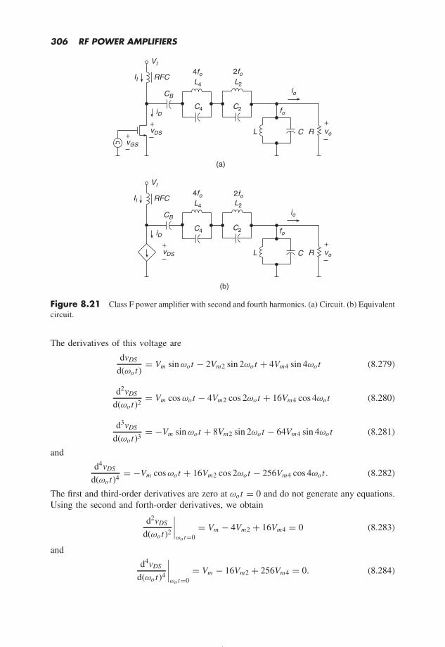
306 RF POWER AMPLIFIERS
(b)
R vo
+vDS
+
VI
L2
C2
L C
RFC
CB
II
iD
io
fo
2fo
(a)
R vo
+vDS
+
VI
L2
foC2
L C
RFC
CB
vGS
+
II
iD
io
2foL4
C4
4fo
L4
C4
4fo
Figure 8.21 Class F power amplifier with second and fourth harmonics. (a) Circuit. (b) Equivalentcircuit.
The derivatives of this voltage are
dvDS
d(ωot)= Vm sin ωot − 2Vm2 sin 2ωot + 4Vm4 sin 4ωot (8.279)
d2vDS
d(ωot)2= Vm cos ωot − 4Vm2 cos 2ωot + 16Vm4 cos 4ωot (8.280)
d3vDS
d(ωot)3= −Vm sin ωot + 8Vm2 sin 2ωot − 64Vm4 sin 4ωot (8.281)
and
d4vDS
d(ωot)4= −Vm cos ωot + 16Vm2 cos 2ωot − 256Vm4 cos 4ωot . (8.282)
The first and third-order derivatives are zero at ωot = 0 and do not generate any equations.Using the second and forth-order derivatives, we obtain
d2vDS
d(ωot)2
∣∣∣∣ωo t=0
= Vm − 4Vm2 + 16Vm4 = 0 (8.283)
and
d4vDS
d(ωo t)4
∣∣∣∣ωo t=0
= Vm − 16Vm2 + 256Vm4 = 0. (8.284)

CLASS F RF POWER AMPLIFIER 307
ωt0
IDM
iD
23π
2π
ωt0
vDS
VI
23π
2π
2π
ωt02
vGS
3π2π
2π
ωt02
vo
3π2π
2π
Vm
2π
0
pD
2π
2π
23π ωt
Figure 8.22 Waveforms in Class F RF power amplifier with second and fourth harmonics peaking.
Solution for this set of equations yields
Vm2 = 5
16Vm (8.285)
Vm4 = 1
64Vm (8.286)

308 RF POWER AMPLIFIERS
and
Vm2 = 20Vm4. (8.287)
Hence,
vDS (0) = VI − Vm + Vm2 − Vm4 = VI − Vm + 5
16Vm − 1
64Vm = VI − 45
64Vm = 0
(8.288)producing
Vm = 64
45VI . (8.289)
Now
vDS (0) = VI − Vm + Vm2 − Vm4 = VI − 16
5Vm2 + Vm2 − 1
20Vm2 = VI − 9
4Vm2 = 0
(8.290)yielding
Vm2 = 4
9VI . (8.291)
Finally,
vDS (0) = VI − Vm + Vm2 − Vm4 = VI − 64Vm4 + 20Vm4 − Vm4 = 0 (8.292)
giving
Vm4 = 1
45VI . (8.293)
The maximum drain-to-source voltage is
VDSM = vDS (π ) = VI + Vm + Vm2 − Vm4 = VI + 64
45VI + 4
9VI − 1
45VI
= 128
45VI ≈ 2.844VI . (8.294)
The normalized maximally flat waveform vDS /VI is given by
vDS
VI= 1 − Vm
VIcos ωot + Vm2
VIcos 2ωot − Vm4
VIcos 4ωot
= 1 − 64
45cos ωot + 4
9cos 2ωot − 1
45cos 4ωot . (8.295)
and is shown in Figure 8.23.The amplitude of the fundamental component of the drain current is
Im = 2
πIDM (8.296)
and
Im = Vm
R= 64
45
VI
R. (8.297)
Thus,
IDM = π
2Im = 32π
45
VI
R. (8.298)
The dc input current is
II = IDM
2= π Im
4= 16π
45
VI
R. (8.299)

CLASS F RF POWER AMPLIFIER 309
−90 −60 −30 0 30 60 90 120 150 180 210 240 2700
0.5
1
1.5
2
2.5
3
ωot (°)
v DS
/VI
n = 1, 2, 4
Figure 8.23 Maximally flat waveform of the drain-to-source voltage vDS /VI for Class F RFpower amplifier with the second and fourth harmonic peaking.
The dc input power is
PI = II VI = 16π
45
V 2I
R. (8.300)
The output power is
PO = V 2m
2R= 2048
2025
V 2I
R. (8.301)
The drain efficiency of the amplifier is
ηD = PO
PI= 128
45π≈ 90.54 %. (8.302)
The maximum drain-to-source voltage is
VDSM = vDS (π )VI + Vm + Vm2 − Vm4 = VI
(1 + 64
45+ 4
9− 1
45
)= 128
45VI ≈ 2.844VI .
(8.303)The output-power capability is
cp = PO
VDSM IDM= ηD PI
VDSM IDM= ηD
(II
IDM
)(VI
VDSM
)
= 128
45π× 1
2× 45
128= 1
2π≈ 0.1592. (8.304)
The dc input resistance is
RDC = VI
II= 45
16πR ≈ 0.8952R. (8.305)

310 RF POWER AMPLIFIERS
8.7.2 Maximum Drain Efficiency Class F24 Amplifier
To find the extrema of the drain-to-source voltage vDS , we take the derivative of this voltageand set the result equal to zero
dvDS
d(ωt)= Vm sin ωot − 2Vm2 sin 2ωot + 4Vm4 sin 4ωot
= Vm sin ωot − 4Vm2 sin ωot cos ωot + 8Vm4 sin 2ωot cos 2ωot
= Vm sin ωot − 4Vm2 sin ωot cos ωot + 16Vm4 sin ωot cos ωot cos 2ωot
= sin ωot(Vm − 4Vm2 cos ωot + 16Vm4 cos ωot cos 2ωot)
= sin ωot[Vm − 4Vm2 cos ωot + 16Vm4 cos ωot(2 cos2 ωot − 1)] = 0. (8.306)
Hence, one solution is
sin ωotm = 0 (8.307)
which gives
ωotm = 0 (8.308)
and
ωotm = π. (8.309)
The second equation is
32Vm4 cos3 ωot − (4Vm2 + 16Vm4) cos ωot + Vm = 0 (8.310)
which can be rearranged to the form
32Vm4
Vmcos3 ωot −
(4
Vm2
Vm+ 16
Vm4
Vm
)cos ωot + 1 = 0. (8.311)
This equation can only be solved numerically. The Fourier coefficients of the drain-to-sourcevoltage waveform vDS for achieving the maximum drain efficiency are [20]
Vm
VI= 1.5 (8.312)
Vm2
VI= 0.389 (8.313)
andVm4
VI= 0.0556. (8.314)
The normalized waveform vDS /VI is given by
vDS
VI= 1 − Vm
VIcos ωot + Vm2
VIcos 2ωot − Vm4
VIcos 4ωot
= 1 − 1.5 cos ωot + 0.5835 cos 2ωot − 0.0834 cos 4ωot . (8.315)
The waveform of vDS /VI for the maximum efficiency is shown in Figure 8.24.The amplitude of the fundamental component of the drain current is
Im = Vm
R= 1.5VI
R. (8.316)
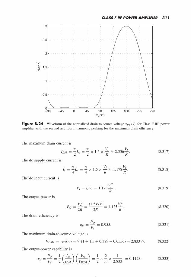
CLASS F RF POWER AMPLIFIER 311
−90 −45 0 45 90 135 180 225 2700
0.5
1
1.5
2
2.5
3
ωot (°)
vD
S /V
I
Figure 8.24 Waveform of the normalized drain-to-source voltage vDS /VI for Class F RF poweramplifier with the second and fourth harmonic peaking for the maximum drain efficiency.
The maximum drain current is
IDM = π
2Im = π
2× 1.5 × VI
R≈ 2.356
VI
R. (8.317)
The dc supply current is
II = π
4Im = π
4× 1.5 × VI
R≈ 1.178
VI
R. (8.318)
The dc input current is
PI = II VI = 1.178V 2
I
R. (8.319)
The output power is
PO = V 2m
2R= (1.5VI )2
2R= 1.125
V 2I
R. (8.320)
The drain efficiency is
ηD = PO
PI= 0.955. (8.321)
The maximum drain-to-source voltage is
VDSM = vDS (π ) = VI (1 + 1.5 + 0.389 − 0.0556) = 2.833VI . (8.322)
The output-power capability is
cp = PO
PI= 1
2
(Im
IDM
)(Vm
VDSM
)= 1
2× 2
π× 1
2.833= 0.1123. (8.323)

312 RF POWER AMPLIFIERS
Table 8.3 Voltage amplitudes in even harmonic maximally flat Class F power amplifiers.
ClassVm
VI
Vm2
VI
Vm4
VI
Vm2
Vm
Vm4
Vm
F24
3= 1.333
1
3= 0.333 0
1
4= 0.25 0
F2464
45= 1.422
4
9= 0.4444
1
45= 0.02222
5
16= 0.3125
1
64= 0.01563
Table 8.4 Voltage amplitudes in even harmonic maximum drain efficiency ClassF power amplifiers.
ClassVm
VI
Vm2
VI
Vm4
VI
Vm2
Vm
Vm4
Vm
F2√
2 = 1.41421
2= 0.5 0
1
4= 0.25 0
F24 1.5 0.5835 0.0834 0.389 0.0556
The dc input resistance is
RDC = VI
II= 0.8489R. (8.324)
The normalized voltage amplitudes in the even harmonic Class F amplifiers that ensure themaximally flat waveform of vDS are given in Table 8.3. The ratios of voltage amplitudesthat give the maximum drain efficiency are given in Table 8.4.
8.8 Class F RF Power Amplifier with Second, Fourth,and Sixth Harmonics
For the maximally flat Class F246 amplifier,
Vm2 = 175
512Vm (8.325)
Vm4 = 7
256Vm (8.326)
Vm6 = 1
512Vm (8.327)
Vm1 = 64
45VI (8.328)
Vm2 = 4
9VI (8.329)
and
Vm4 = 1
45VI . (8.330)

CLASS F RF POWER AMPLIFIER 313
8.9 Class F RF Power Amplifier with Series-resonantCircuit and Quarter-wavelength TransmissionLine
A Class F RF power amplifier with a series-resonant circuit and a quarter-wavelength trans-mission line was introduced in [7] and is shown in Figure 8.25(a). The quarter-wavelengthtransmission line is equivalent to an infinite number of series-resonant circuits, whichbehaves like short circuits for odd harmonics and like open circuits for even harmonics.The equivalent circuit of the amplifier is depicted in Figure 8.25(b). Voltage and currentwaveforms of the amplifier are shown in Figure 8.26. The drain current is a square waveand the drain-to-source voltage is a half-sine wave. The circuit and its waveforms are dualto those of the Class F amplifier with a parallel-resonant circuit. The drain current and thedrain-to-source voltage waveforms are interchanged. This circuit will be referred to as theClass Fs amplifier or Class F inverse amplifier.
The drain current is a square wave and it can be expanded into a Fourier series
iD = IDM
1
2+ 2
π
[cos ωot − 1
3cos 3ωot + 1
5cos 5ωot − 1
7cos 7ωot + · · ·
]. (8.331)
The drain current iD contains only the dc component, fundamental component, and oddharmonic components.
vDS+
IIRFC
VI
λ4
vo
L C
iD
vGS
+ +R
vDS+
II RFC
VI
vo
L CiD
vGS
+
+
R
fo
(a)
(b)
5fo 3fo(2k +1)fo
Figure 8.25 Class F power amplifier employing a series-resonant circuit and a quarter-wavelengthtransmission line, where n = 2k + 1 with k = 0, 1, 2, . . . . (a) Circuit. (b) Equivalent circuit at Zo = R.

314 RF POWER AMPLIFIERS
ωt0
IDM
iD
23π
2π
ωt023π
2π
2π
ωt02
vGS
3π2π
2π
ωt02
vo
3π2π
2π
2π
VDSM
vDS
Figure 8.26 Voltage and current waveforms in Class F RF power amplifier with a series-resonantcircuit and a quarter-wavelength transmission line [7].
The drain-to-source voltage waveform vDS can be expanded into a Fourier trigonometricseries
vDS = VDSM
[1
π+ 1
2cos ωot + 2
π
∞∑n=2
cos( nπ
2
)1 − n2
cos nωot
]
= VDSM
[1
π+ 1
2cos ωot + 2
3πcos 2ωot − 2
15πcos 4ωot + 2
35πcos 6ωot + · · ·
].
(8.332)Thus, the drain current waveform iD contains only the dc component, fundamental compo-nent, and the even harmonic components.
The output voltage is equal to the fundamental component of the drain-to-source voltage
vo = −Vm cos ωot (8.333)
where
Vm = VDSM
2= π
2VI . (8.334)

CLASS F RF POWER AMPLIFIER 315
The output current is equal to the fundamental component of the drain current
io = id1 = Im cos ωot (8.335)
whereIm = 2
πIDM = 4
πII (8.336)
or
Im = Vm
R= πVI
2R. (8.337)
The dc supply current is equal to the dc component of the drain current
II = IDM
2= π
4Im = π2VI
8R. (8.338)
and dc supply voltage is
VI = VDSM
π. (8.339)
Hence, the dc supply power is
PI = II VI = IDM VI
2= IDM VDSM
2π. (8.340)
The output power is
PO = 1
2ImVm = 1
2× 2
π× IDM
VDSM
2= 1
2πIDM VDSM (8.341)
or
PO = V 2m
2R= π2V 2
I
8R. (8.342)
The efficiency of the amplifier is
η = PO
PI= 1. (8.343)
The output-power capability is
cp = PO
IDM VDSM= 1
2π= 0.159. (8.344)
The dc resistance is
RDC = VI
II= 8
π2R ≈ 0.811R. (8.345)
The input impedance of the load network seen by the drain and source terminals at thefundamental frequency fo is
Z (fo ) = Vm
Im= Ri = Z 2
o
R; (8.346)
the impedance at even harmonics is
Z (nfo ) = Z (2kfo ) = Vm(n)
Im(n)= finite value
0= ∞ for n = 2, 4, 6, . . . (8.347)
and the impedance at odd harmonics is
Z (nfo ) = Z [(2k + 1)fo] = Vm(n)
Im(n)= 0
finite value= 0 for n = 3, 5, 7, . . . (8.348)
where k = 1, 2, 3, . . . .

316 RF POWER AMPLIFIERS
The rms value of the drain current is
IDSrms =√
1
2π
∫ π/2
π/2I 2DM d(ωo t) = IDM√
2. (8.349)
If the transistor is operated as a switch, the conduction loss in the MOSFET on-resistancerDS is given by
PrDS = rDS I 2DSrms = rDS I 2
m
2= π2
8rDS I 2
m . (8.350)
The output power is
PO = rDS I 2m
2. (8.351)
Thus, the drain efficiency is
ηD = PO
PI= PO
PO + PrDS= 1
1 + PrDS
PO
= 1
1 + π2
4
rDS
Ri
. (8.352)
Example 8.6
Design a Class F power amplifier with a quarter-wave transmission line to deliver a powerof 10 W at fc = 5 GHz. The required bandwidth is BW = 500 MHz. The dc power supplyvoltage is 28 V and VDSmin = 1 V. The load resistance is R = 50 . The MOSFET on-resistance is rDS = 0.2 .
Solution. The maximum amplitude of the fundamental component of the drain-to-sourcevoltage is
Vm = π
2(VI − VDSmin ) = π
2(28 − 1) = 42.41 V. (8.353)
The input resistance of the load circuit is
Ri = V 2m
2PO= 42.412
2 × 10= 89.93 . (8.354)
The maximum drain-to-source voltage is
VDSmax = πVI = π × 28 = 87.965 V. (8.355)
The amplitude of the fundamental component of the drain current is
Im = Vm
Ri= 42.41
89.93= 0.472 A. (8.356)
The maximum drain current is
IDM = π
2Im = π
2× 0.472 = 0.7414 A. (8.357)
The dc supply current is
II = IDM
2= 0.7414
2= 0.37 A. (8.358)
The dc supply power is
PI = II VI = 0.37 × 28 = 10.36 W. (8.359)

CLASS F RF POWER AMPLIFIER 317
The drain power loss of the transistor is
PD = PI − PO = 10.36 − 10 = 0.36 W. (8.360)
The drain efficiency is
ηD = PO
PI= 10
10.36= 96.525 %. (8.361)
The dc resistance presented by the amplifier to the dc source is
RDC = 8
π2R = 0.81 × 89.93 = 72.84 . (8.362)
The characteristic impedance of the transmission line is
Zo =√
Ri R = √89.93 × 50 = 67 . (8.363)
Assume the dielectric constant used for construction of the transmission line to be εr = 2.1.The wavelength in the transmission line is
λ = c√εr fc
= 3 × 10⁸
√2.1 × 5 × 109
= 4.14 cm. (8.364)
Hence, the length of the transmission line is
lTL = λ
4= 4.14
4= 1.035 cm. (8.365)
The loaded quality factor is
QL = fcBW
= 5 × 10⁹
500 × 106= 10. (8.366)
The loaded quality factor for a series-resonant circuit is defined as
QL = ωcL
R= ωcCR. (8.367)
Hence, the inductance of the resonant circuit tuned to the fundamental is
L = QLR
ωc= 10 × 50
2π × 5 × 109= 15.915 nH. (8.368)
The capacitance of the resonant circuit is tunned to the fundamental frequency is
C = 1
ωcQLR= 1
2π × 5 × 109 × 10 × 50= 0.06366 pF. (8.369)
The drain efficiency is
ηD = 1
1 + π2
4
rDS
Ri
= 1
1 + π2
4
0.2
89.93
= 99.45 %. (8.370)
8.10 Summary
• The drain efficiency and the output-power capability for Class F RF power amplifiers aregiven in Table 8.5, where ηD(MF ) and cp(MF ) are the drain efficiency and the output-powercapability for the maximally flat waveform of vDS , respectively, and Bs is the Class Bamplifier with rectangular drain current and sinusoidal drain-to-source voltage.
• The load network in Class F RF power amplifiers has resonant circuits tuned to thefundamental frequency and to one or more harmonic frequencies.

318 RF POWER AMPLIFIERS
Table 8.5 Drain efficiencies and output power capabilities of Class F power amplifiers.
Class ηD(MF ) ηDmax cp(MF ) cpmax
B –π
4= 78.54 % –
1
8= 0.125
F39π
32= 88.36 %
π
2√
3= 90.67 %
9
64= 0.1406
1
4√
3= 0.1443
F3575π
256= 90.23 % 92.04 %
225
1536= 0.1465 0.2071
F28
3π= 84.88 %
2√
2
π= 90.03 %
1
2π= 0.1592
√2
π (√
2 + 1.5)= 0.1545
F24128
45π= 90.54 % 95.5 %
1
2π= 0.1592 0.1061
F∞ 100 % 100 %1
2π= 0.1592
1
2π= 0.1592
Bs –2
π= 63.67 % –
1
2π= 0.1592
• The addition of harmonics of the correct amplitudes and phases into the drain-to-sourcevoltage flattens the vDS voltage, reducing the transistor loss and improving the efficiency.
• The circuit diagram of the Class F power amplifier is complex.
• The Class F RF power amplifier consists of a transistor and a parallel or series resonantcircuit tuned to the fundamental frequency and resonant circuits tuned to the harmonics.
• The transistor in the Class F amplifier with third harmonic or with third and fifth harmonicis operated as a dependent current source.
• The conduction angle of the drain or collector current in the Class F power amplifier isusually 180.
• The drain efficiency of the idealized Class F power amplifier at VDSmin = 0 for themaximally flat waveform of vDS (1) with the third harmonic is 88.36 %, (2) with thethird and fifth harmonics is 90.23 %, (3) with the second harmonic is 84.88 %, (4) withthe second and fourth harmonics is 90.54 %, and (5) and with the transmission line is100 %.
• The maximum drain efficiency of the idealized Class F power amplifier (1) with the thirdharmonic is 90.67 %, (2) with the third and fifth harmonics is 92.04 %, and (3) with thesecond harmonic is 90.03 %.
• The Class F power amplifier with a parallel-resonant circuit and a quarter-wavelengthtransmission line ideally has a square wave drain-to-source voltage vDS and a half-sinusoidal drain current iD .
• The Class F power amplifier with a series resonant-circuit and a quarter-wavelengthtransmission line forms a square-wave drain current iD and a half-sinusoidal drain-to-source voltage vDS .
• Transmission lines can be used to create higher-order harmonics in Class F power ampli-fiers.
• There is a trade-off between the efficiency and circuit complexity of Class F amplifiers.

CLASS F RF POWER AMPLIFIER 319
• The transistor output capacitance can dominate the total impedance of the output net-work and hamper the synthesis of the desired output network with high impedances atharmonics in the Class F power amplifiers.
8.11 References
[1] V. J. Tyler, ‘A new high-efficiency high-power amplifier,’ Marconi Review, vol. 21, no. 130,pp. 96–109, Fall 1958.
[2] D. M. Snider, ‘A theoretical analysis and experimental confirmation of the optimally loadedand over-driven RF power amplifier,’ IEEE Trans. Electron Devices, vol. 14, pp. 851–857, June1967.
[3] V. O. Stocks, Radio Transmitters: RF Power Amplification, London, England: Van Nostrand,1970, pp. 38–48.
[4] N. S. Fuzik, ‘Biharmonic modes of tuned power amplifier,’ Telecommunications and RadioEngineering, Part 2, vol. 25, pp. 117–124, 1970.
[5] S. R. Mazumber, A. Azizi, and F. E. Gardiol, ‘Improvement of a Class C transistor poweramplifiers by second-harmonic tuning,’ IEEE Transactions on Microwave Theory and Technique,vol. 27, no, 5, pp. 430–433, May 1979.
[6] H. L. Krauss, C. V. Bostian, and F. H. Raab, Solid State Radio Engineering, New York, NY:John Wiley & Sons, 1980.
[7] M. K. Kazimierczuk, ‘A new concept of Class F tuned power amplifier,’ Proc. 27-th MidwestSymposium on Circuits and Systems, Morgantown, WV, June 11–12, 1984, pp. 425–428.
[8] Z. Zivkovic and A. Markovic, ‘Third harmonic injection increasing the efficiency of high powerRF amplifiers,’ IEEE Trans. Broadcasting, vol. 31, no. 2, pp. 34–39, May 1985.
[9] Z. Zivkovic and A. Markovic, ‘Increasing the efficiency of high power triode RF amplifier. Whynot with the second harmonic?,’ IEEE Trans. Broadcasting, vol. 32, no. 1, pp. 5–10, March1986.
[10] X. Lu, ‘An alternative approach to improving the efficiency of the high power radio frequencyamplifiers,’ IEEE Trans. Broadcasting, vol. 38, pp. 85–89, June 1992.
[11] F. H. Raab, ‘An introduction to Class-F power amplifiers,’ RF Design, vol. 19, no. 5, pp. 79–84,March 1996.
[12] F. H. Raab, ‘Class-F power amplifiers with maximally flat waveforms,’ IEEE Trans. MicrowaveTheory and Technique, vol. 45, no. 11, pp. 2007–2012, November 1997.
[13] B. Tugruber, W. Pritzl, D. Smely, M. Wachutka, and G. Margiel, ‘High-efficiency harmoniccontrol amplifier,’ IEEE Trans. Microwave Theory and Technique, vol. 46, no. 6, pp. 857–862,June 1998.
[14] F. H. Raab, ‘Class-F power amplifiers with reduced conduction angle,’ IEEE Trans. Broadcast-ing, vol. 44, no. 4, pp. 455–459, December 1998.
[15] C. Trask, ‘Class-F amplifier loading networks: a unified design approach,’ IEEE MTT-S Dig.,pp. 351–354, June 1999.
[16] S. C. Cripps, RF Power Amplifiers for Wireless Communications, Atrech House, Norwood, MA,1999.
[17] P. Colantonio, F. Guannini, G. Leuzzi, and E. Limiti, ‘On the class-F power amplifier design,’RF Microwave Computer-Aided Eng., vol. 32, no. 2, pp. 129–149, Mar. 1999.
[18] A. N. Rudiakova, V. G. Krizhanovski, and M. K. Kazimierczuk, ‘Phase tuning approach topolyharmonic power amplifiers, Proc. European Microwave Week Conference, London, UK,September 10–14, 2001, pp. 105–107.
[19] F. Fortes and M J. Rosario, ‘A second harmonic Class-F power amplifier in standard CMOStechnology,’ IEEE Trans. Microwave Theory and Technique, vol. 49, no. 6, pp. 1216–1220, June2001.
[20] F. H. Raab, ‘Maximum efficiency and output of Class-F power amplifiers,’ IEEE Trans.Microwave Theory and Technique, vol. 49, no. 6, pp. 1162–1166, June 2001.

320 RF POWER AMPLIFIERS
[21] F. H. Raab, ‘Class-E, Class-C, and Class-F power amplifiers based upon a finite number ofharmonics,’ IEEE Trans. Microwave Theory and Technique, vol. 49, no. 8, pp. 1462–1168,August 2001.
[22] F. Lepine, A. Adahl, and H. Zirath, ‘L-band LDMOS power amplifier based on an inverse ClassF architecture,’ IEEE Trans. Microwave Theory and Technique, vol. 53, no. 6, pp. 2007–2012,June 2005.
[23] A. Grebennikov, RF and Microwave Power Amplifier Design, New York, NY: McGraw-Hill,2005.
[24] A. N. Rudiakova and V. G. Krizhanovski, Advanced Design techniques for RF Power Amplifiers,Springer, 2006.
8.12 Review Questions
8.1 What is the principle of operation of Class F RF power amplifiers?
8.2 What is the topology of the Class F power amplifier?
8.3 Are the topologies of Class F power amplifiers simple or complex?
8.4 What is the mode of operation of the transistor in the Class F power amplifier?
8.5 How high is the efficiency of Class F power amplifiers?
8.6 What should be the amplitude of the third harmonic voltage in the Class F amplifierwith the third harmonic peaking?
8.7 How can the transmission lines be used to control the impedances at harmonics inClass F power amplifiers?
8.8 What are the applications of the Class F RF power amplifiers?
8.9 Does the transistor output capacitance affect the operation of Class F RF poweramplifiers?
8.10 List the applications of Class F RF power amplifiers.
8.13 Problems
8.1 Design a Class F power amplifier employing third-harmonic peaking with a maximallyflat drain-to-source voltage to deliver a power of 100 W at f = 2.4 MHz. The dc powersupply voltage is 120 V and VDSmin = 1 V.
8.2 Design a Class F power amplifier employing third-harmonic peaking with maximallydrain efficiency to deliver a power of 100 W at f = 2.4 MHz. The dc power supplyvoltage is 120 V and VDSmin = 1 V.
8.3 Design a Class F power amplifier employing second-harmonic peaking with a maxi-mally flat drain-to-source voltage to deliver a power of 1 W at f = 2.4 MHz. The dcpower supply voltage is 5 V and VDSmin = 0.3 V.
8.4 Design a Class F3 RF power amplifier to meet the following specifications: VI = 48 V,PO = 100 W, VDSmin = 2 V, θ = 60, RL = 50 , fc − 88 MHz, and BW = 10 MHz.

9Linearization and EfficiencyImprovement of RF PowerAmplifiers
9.1 Introduction
High efficiency and high linearity of power amplifiers are of primary importance in wirelesscommunications systems [1–41]. High efficiency is required for low energy consumption,a longer battery lifetime, and thermal management. Linearity is required for achieving lowdistortion of the amplified signals. The RF power amplifier specifications call for IM levelsof −60 dBc. Linearity and efficiency enhancement techniques of RF power amplifiers, whichare used in transmitters, are studied in this chapter. Signals used in modern communicationssystems have a time-varying envelope and time-varying angle. A nonconstant envelopesignal requires linear power amplifiers in the transmitters. The output power in CDMA2000and WCDMA transmitters may vary in a wide dynamic range of 80 dB. The averageoutput power is usually lower than the peak power by 15–25 dB. The transmitters mustbe designed for the maximum output power. The maximum efficiency of linear poweramplifiers such as Class A, AB, and B amplifiers occurs at the maximum output power. Inthis case, the maximum amplitude of the drain-to-source voltage Vm is nearly equal to thesupply voltage VI . This corresponds to the AM modulation index equal to 1. However, theaverage AM modulation index is in the range of 0.2–0.3, when the amplitude of the drain-to-source voltage Vm is much lower than the supply voltage VI . Therefore, the statisticalaverage efficiency of linear power amplifiers with AM modulation is much lower thantheir maximum efficiency. In wireless communications, there are two types of transmitters:base-station transmitters and handset transmitters.
Ideal characteristics of a power amplifier are depicted in Figure 9.1. The efficiency η
should be very high over a wide range of the output power, as shown in Figure 9.1(a).The output voltage vo should be a linear function of the input voltage vi , as shown in
RF Power Amplifiers Marian K. Kazimierczuk 2008 John Wiley & Sons, Ltd

322 RF POWER AMPLIFIERS
(a)Po
η
0
vi
vo
0
(b)
Figure 9.1 Ideal characteristics of a power amplifier. (a) Efficiency η as a function of the outputpower. (b) Output voltage vo as a function of the input voltage vi .
Figure 9.1(b). In this case, the voltage gain of the amplifier Av = vo/vi is constant over awide range of the input voltage.
Power control of RF transmitters is required in modern digital wireless communications.In CDMA, power control is used in both base-station transmitters and handset transmitters.In base-station transmitters, a higher power is required to transmit the signal to the edgesof a cell. In handset transmitters, the output power should be transmitted at variable levelsso that the power levels of the signals received at the base station are similar for all users.
9.2 Predistortion
Nonlinear distortion in the output signal of a power amplifier is caused by changes inthe slope of the transfer function vo = f (vi ). These changes are caused by the nonlinearproperties of transistors (MOSFETs or BJTs) used in the power amplifier. The changes inthe slope of the transfer function cause changes in the gain at different values of the inputvoltage or power. There are several techniques for reduction of nonlinear distortion.
Predistortion is a technique that seeks to linearize a power amplifier by making suitablemodifications to the amplitude and phase of the power amplifier input signal. A block dia-gram of a power amplifier with predistortion is depicted in Figure 9.2. A nonlinear block isconnected in the signal path to compensate for the nonlinearity of the power amplifier. Thisblock is called a predistorter or a predistortion linearizer. Predistortion can be performedeither at RF or baseband frequencies. Predistortion at baseband frequencies is favorablebecause of digital signal processing (DSP) capabilities. This is called ‘digital predistortion.’
voviPA
PredistortionLinearizer
Figure 9.2 Block diagram of power amplifier with a predistortion system.

LINEARIZATION AND EFFICIENCY IMPROVEMENT 323
DSP ICs can be used to perform digital predistortion. It is an open-loop system, which isinherently stable. The disadvantage of the system is the difficulty in generating the transferfunction of the predistorter such that the transfer function of the overall system is linear.
Example 9.1
A power amplifier voltage transfer function has the gain A1 = 100 for small signals andthe gain A2 = 50 for large signals, as depicted in Figure 9.3(a). Find the transfer functionof the predistorter to achieve a linear transfer function of the overall system.
Solution. Let us assume the gain of the predistorter for small signals to be A3 = 1. Theratio of the two gains of the power amplifiers is
A1
A2= 100
50= 2. (9.1)
Hence, the gain of the predistorter for large signals is
A4 = 2. (9.2)
(c)
vo
A1
(a)
A2
vi
0
vip
vop
0A3
A4
A
A1
(b)
A2
vi0
A
A4
(d)
A3 =1
vip0
vit
vot
0
(e)
A5
A6
vit
A
0
(f)
A5, A6
Figure 9.3 Transfer functions of a power amplifier using predistortion. (a) Nonlinear transferfunction of a power amplifier vo = f (vi ). (b) Transfer function of the predistorter A. (c) Transfer func-tion of the predistorter vop = f (vip). (d) Transfer function of a predistortion amplifier Ap . (e) Transferfunction of the total amplifier A. (f) Linearized transfer function of the overall system vot = f (vit ).

324 RF POWER AMPLIFIERS
The gain of the overall system for low signals is
A5 = A1A3 = 100 × 1 = 100 (9.3)
and for large signals is
A6 = A2A4 = 50 × 2 = 100. (9.4)
Thus, A6 = A5, resulting in a linear transfer function over a wide range of the input sig-nal. Figure 9.3 illustrates the linearization of a power amplifier using the predistortiontechnique.
9.3 Feedforward Linearization Technique
A block diagram of a basic power amplifier system with feedforward linearization technique[1–6] is shown in Figure 9.4(a). The feedforward linearization technique relies on thecancellation of the distortion signal. This is done by generating a proper error voltage and
veo
vp
vo
+
ve+
Av
vp
Av
vi
va
vi
Main Power Amplifier
1/Av
ErrorAmplifier
ErrorAmplifier
vo
+
ve+
Av
AvTpd
vi
(a)
Ted
(b)
1/Av
Figure 9.4 Block diagram of a power amplifier system with feedforward linearization. (a) Basicfeedforward system. (b) Feedforward system with delay blocks.

LINEARIZATION AND EFFICIENCY IMPROVEMENT 325
subtracting it from the distorted output voltage of a nonlinear power amplifier. The inputvoltage vi is applied to two channels. The voltage in one channel is applied to the input ofthe main power amplifier with the voltage gain Av and it is amplified. The other channeluses the original input voltage vi as a reference signal for future comparison. The outputvoltage of the main power amplifier containsthe undistorted and amplified input voltageAv vi and the distortion voltage vd produced by the amplifier nonlinearity
vp = Av vi + vd . (9.5)
The total output voltage of the main power amplifier is attenuated by a circuit with thetransfer function equal to 1/Av
va = vp
Av= vi + vd
Av. (9.6)
The attenuated voltage is compared with the original voltage vi in the subtractor to producean error voltage ve :
ve = va − vi = vi + vd
Av− vi = vd
Av. (9.7)
The error voltage ve is amplified by the error amplifier with the voltage gain Av , yielding
veo = Av ve = Avvd
Av= vd . (9.8)
Next, the output voltage of the main power amplifier vp is compared with the error amplifieroutput voltage veo by a subtractor, producing the output voltage of the entire system
vo = vp − veo = Av vi + vd − vd = Av vi . (9.9)
It can be seen that the distortion signal vd is cancelled out for perfect amplitude and phasematching at each subtractor. In addition to the cancellation of the nonlinear component,the system suppresses the noise added to the signal in the main power amplifier. Thefirst loop is called the signal cancellation loop and the second loop is called the errorcancellation loop.
The feedforward linearization system offers a wide bandwidth, reduced noise level, andis stable in spite of large phase shifts at RF because the output signal is not applied tothe input. Wideband operation is useful in multicarrier wireless communications such aswireless base stations.
The main disadvantage of the feedforward linearization system is the gain mismatch andthe phase (delay) mismatch in the signal channels. The amount of linearization depends onthe amplitude and phase matching at each subtractor. If the firstloop from the input voltagevi to the first subtractor has a relative gain mismatch A/A and the phase mismatchφ, the attenuation of the magnitude of the intermodulation terms in the output voltageis [2, 4]
AIM =√
1 − 2
(1 + A
A
)cos φ +
(1 + A
A
)2
. (9.10)
To improve the signal quality, delay blocks can be added as shown in Figure 9.4(b). Adelay block Tpd is added in the bottom path to compensate for the delay introduced by themain power amplifier and the attenuator. The other delay block Ted is added in the upperpath to compensate for the delay introduced by the error amplifier. The delay blocks canbe implemented using passive lumped-element networks or transmission lines. However,these blocks dissipate power and reduce the amplifier efficiency. In addition, the design ofwideband delay blocks is difficult.

326 RF POWER AMPLIFIERS
9.4 Negative Feedback Linearization Technique
A block diagram of a power amplifier with a negative feedback is depicted in Figure 9.5.The transfer function vo = f (vs ) of a power amplifier can be considerably linearized throughthe application of negative feedback, reducing nonlinear distortion. Large changes in theopen-loop gain cause much smaller changes in the closed-loop gain.
Let us assume that the output voltage of a power amplifier without negative feedbackcontains a distortion component (an intermodulation term of a harmonic) given by
vd = Vd sin ωd t . (9.11)
The distortion component of the output voltage of the power amplifier with negative feed-back is
vdf = Vdf sin ωd t . (9.12)
We wish to find the relationship between vd and vdf . The feedback voltage is
vf = βvdf . (9.13)
The reference voltage for the distortion component is zero. Hence, the input voltage of thepower amplifier is
ve = −vf = −βvdf . (9.14)
The distortion component at the power amplifier output is
vod = Ave = −Avf = −βAvdf . (9.15)
Thus, the output voltage contains two terms: the original distortion component generatedby the power amplifier vd andthe component vod , which represents the effect of negativefeedback. Hence, the overall output voltage is
vdf = vd − vod = vd − βAvdf (9.16)
yieldingvdf = vd
1 + βA= vd
1 + T. (9.17)
Since A is generally a function of frequency, the amplitude of the distortion componentmust be evaluated at the frequency of the distortion component fd = ωd/(2π ).
It follows from (9.17) that the nonlinear distortion reduction is large when the loop gainT = βA is high. However, the voltage gain of RF power amplifiers is low, and thereforethe loop gain T is also low at RF. In addition, stability of the loop is of great concerndue to a large number of poles introduced by various parasitic components. A high-orderpower amplifier may have an excessive phase shift, causing oscillations. For a large loopgain T = βA,
Af ≈ 1
β. (9.18)
vovs A
β
+
vf
ve
Figure 9.5 Block diagram of a power amplifier system with negative feedback.

LINEARIZATION AND EFFICIENCY IMPROVEMENT 327
vf
vi +PA
LPF
sin ωLOtsin (ωLOt + φ)
vo
Figure 9.6 Block diagram of a power amplifier system with negative feedback linearization.
This equation indicates that the gain depends only on the linear feedback network β. Theoutput voltage of a power amplifier is given by
vo = Af vs ≈ vi
β. (9.19)
Thus, the transfer function is nearly linear. However, the feedback amplifier requires alarger input voltage in order to produce the same output as the amplifier without feed-back.
Figure 9.6 shows a block diagram of a power amplifier with negative feedback andfrequency translation. The forward path consists of a low-frequency high-gain error ampli-fier, an up-conversion mixer, and a power amplifier. The mixer converts the frequency ofthe input signal fi to an RF frequency fRF = fi + fLO , where fLO is the frequency of thelocal oscillator. The feedback path consists of a down-conversion mixer and a low-passfilter (LPF). The mixer converts the frequency of the RF signal fRF to the input frequencyfi = fRF − fLO . In this system, ahigh loop gain T is obtained at low frequencies. There-fore, the negative feedback is very effective in reducing the nonlinear distortion. The totalphase shift in the upper path by the error amplifier, the mixer, and the power amplifierusually exceeds 180. Therefore, a phase shift is added to the local oscillator to ensure loopstability.
Example 9.2
An open-loop power amplifier has a gain A1 = 100 for small signals and a gain A2 = 50.The transfer function of the feedback network is β = 0.1. Find the closed-loop gains of thepower amplifier with negative feedback.
Solution. The ratio of the open-loop gains is
A1
A2= 100
50= 2. (9.20)
The relative change in the gain of the open-loop power amplifier is
A1 − A2
A1= 100 − 50
100= 50 %. (9.21)
The loop gain for small signals is
T1 = βA1 = 0.1 × 100 = 10 (9.22)
and the closed-loop gain for small signals is
Af 1 = A1
1 + T1= 100
1 + 10= 9.091. (9.23)

328 RF POWER AMPLIFIERS
Af1 Af2
(c)
vs
vo
A1
(a)
A2
vof
Af1
Af2
vi
0
0
(d)
vs
A
A1
(b)
Af
vi
0
0
A2
Figure 9.7 Transfer functions of a power amplifier without and with negative feedback.(a) Transfer function vo = f (vi ) without negative feedback. (b) Transfer function A without nega-tive feedback. (c) Transfer function Vof = vs with negative feedback. (d) Transfer function Af withnegative feedback.
The loop gain for large signals is
T2 = βA2 = 0.1 × 50 = 5 (9.24)
and the closed-loop gain for large signals is
Af 2 = A2
1 + T2= 50
1 + 5= 8.333. (9.25)
The ratio of the closed-loop gain is
Af 1
Af 2= 9.091
8.333= 1.091. (9.26)
The relative change in the gain of the closed-loop power amplifier is
Af 1 − Af 2
Af 1= 9.091 − 8.333
9.091= 8.333 %. (9.27)
Thus, the open-loop transfer function changes by a factor of 2, whereas the closed-looptransfer function changes by a factor of 1.091. Figure 9.7 illustrates the linearization of apower amplifier using the negative feedback technique.
Example 9.3
The relationship between the input voltage ve and the output voltage vo of a power stageof an RF amplifier is given by
vo = Av 2e . (9.28)

LINEARIZATION AND EFFICIENCY IMPROVEMENT 329
0 0.2 0.4 0.6 0.8 10
10
20
30
40
50
60
70
80
90
100
ve (V)
v o (
V)
Figure 9.8 Output voltage as a function of input voltage for a power amplifier without negativefeedback.
0 2 4 6 8 10 120
10
20
30
40
50
60
70
80
90
100
vs (V)
v o (
V)
Figure 9.9 Output voltage as function of input voltage for a power amplifier with negativefeedback.
330 RF POWER AMPLIFIERS
Find the relationship between the input voltage vs and the output voltage vo for the RFamplifier with negative feedback. Draw the plots of vo = f (ve) and vo = f (vs ) for A = 100and β = 1/10.
Solution. The error voltage is
ve = vs − βvo . (9.29)
Hence, the output voltage with negative feedback is
vo = A(vs − βvo)2. (9.30)
Solving for vs , we get
vs = βvo +√
vo
A(9.31)
or
vo = vs
β− 1
β
√vo
A. (9.32)
Figures 9.8 and 9.9 illustrates the linearization of a power amplifier using the negativefeedback technique. It can be seen that the plot of the amplifier with negative feedback ismuch more linear.
9.5 Envelope Elimination and Restoration
A block diagram of a power amplifier with an envelope elimination and restoration system(EER) is shown in Figure 9.10. The concept of the EER system was first presented byKahn in 1952 [8]. It has been used to increase linearity and efficiency of radio transmitters.One path of the EER system consists of an RF limiter and an RF nonlinear high-efficiencyswitching-mode power amplifier. The other path consists of an envelope detector and anAM modulator, which is a low-frequency power amplifier.
An amplitude modulated (AM) and phase modulated (PM) voltage applied to the amplifierinput can be represented by
vi = V (t) cos[ωct + θ (t)]. (9.33)
vPM
Avvmvm
vi
LF PA Modulator
AvEnvelopeDetector
Limiter
SwitchingRF PA
Figure 9.10 Block diagram of power amplifier with envelope elimination and restoration (EER).

LINEARIZATION AND EFFICIENCY IMPROVEMENT 331
This voltage is applied to both an RF limiter and an envelope detector. The output voltageof an RF limiter is a constant-envelope phase-modulated (CE PM) voltage
vPM = Vc cos[ωct + θ (t)]. (9.34)
The RF limiter should be designed to minimize amplitude-to-phase conversion. The outputvoltage of an envelope detector is
vm (t) = V (t). (9.35)
The envelope of the input voltage is extracted using an envelope detector, usually a diodeAM detector to obtain the AM modulating voltage vm (t). Next, it is amplified by a low-frequency power amplifier with the voltage gain Av , producing a modulating voltageAv vm (t). The envelope is eliminated from the AM-PM voltage using a limiter. The PMvoltage vPM is simultaneously amplified and amplitude modulated by an RF power ampli-fier to restore the original amplitude and phase information contained in the input signal vi .The PM voltage vPM is applied to the gate of the transistor in the RF power amplifier andthe modulating voltage vm is used to modulate the supply voltage of the RF power ampli-fier, producing vDD = vm (t)Av VDD . In switching-mode RF power amplifiers, the amplitudeof the output voltage is directly proportional to the supply voltage VDD . A very importantadvantage of the EER system is that a linear RF power amplifier is not required. Linear RFpower amplifiers exhibit very low efficiency, which decreases when the AM modulationindex decreases. The average AM modulation index is in the range from 0.2 to 0.3. Ahighly efficient nonlinear RF power amplifier can be used in the EER system. Switching-mode RF power amplifiers, such as Class D, E, DE, and F amplifiers, exhibit a very highefficiency, greater than 90 %. Their efficiency is approximately independent of the AMmodulation index. An amplitude-modulated high-efficiency Class E power amplifier wasstudied in [15].
The EER system suffers from a couple of shortcomings. First, there is mismatch betweenthe total phase shift (delay) and gain in the two paths. It is a hard task because the phaseshift in the low-frequency path is much larger than that in the high-frequency path. Theintermodulation term due to the phase mismatch is given by [10]
IDM ≈ 2πBW 2RF τ 2 (9.36)
where BWRF is the bandwidth of the RF signal and τ is the delay mismatch.Second, phase distortion is introduced by the limiter. Limiters are built using nonlinear
devices and exhibit a considerable AM-to-PM conversion at high frequencies, corrupting thephase θ (t) of the PM signal vPM . Third, the phase distortion is introduced by the nonlineartransistor capacitance due to the AM modulation of the supply voltage of the RF poweramplifier.
9.6 Envelope Tracking
The main goal of the envelope tracking technique is to maintain a high efficiency over awide range of the input power. A block diagram of a power amplifier with envelope tracking(ET) is shown in Figure 9.11 [17–21]. This system is also called a power amplifier withadaptive biasing or a power amplifier with dynamic control of supply voltage. The systemconsists of two paths. One path contains a linear power amplifier and a delay block Td . Theother path consists of an envelope detector and a dc-dc switching-mode power converter.The ET system is similar to the EER system, but it uses a linear power amplifier anddoes not have an RF limiter as the EER system does. Instead of modulating the RF power

332 RF POWER AMPLIFIERS
vi Av
EnvelopeDetector
DC/DCConverter
LinearPA
Td
VI
Figure 9.11 Block diagram of power amplifier with envelope tracking (ET).
amplifier, it adjusts the level of the supply voltage so that Vm/VI is always close to 1 toallow efficient linear amplification.
The drain efficiency of current-mode power amplifiers decreases as the amplitude ofthe drain-to-source voltage Vm decreases. In the current-mode power amplifiers, such asClass A, AB, B, and C amplifiers, the transistor is operated as a dependent current source.In these amplifiers, the amplitude of the drain-to-source voltage Vm is proportional to theamplitude of the input voltage Vim . The drain efficiency of the power amplifiers at theresonant frequency is given by
ηD = PDS
PI= 1
2
(Im
II
)(Vm
VI
). (9.37)
It can be seen from this equation that the drain efficiency ηD is proportional to the ratioVm/VI . As Vm decreases due to an increase in Vim at fixed value of the supply voltage VI ,the ratio Vm/VI also decreases, reducing the drain efficiency. If the supply voltage VI isincreased proportionally to the amplitude of the input voltage Vim , the ratio Vim/VI , thenthe ratio Vm/VI can be maintained at a fixed value close to 1 (e.g., 0.9), resulting in highefficiency at any amplitude Vm . When Vim is varied in current-mode power amplifiers, theconduction angle of the drain current remains approximately constant and the ratio Im/II
is also constant. For instance, for the Class B amplifier, Im/II = π/2. The efficiency isimproved, while low distortion of the RF linear power amplifier is preserved.
9.7 The Doherty Amplifier
The Doherty power amplifier was first proposed in 1936 [23]. The main purpose of thissystem is to maintain high efficiency over a wide range of the input voltage of a linearpower amplifier with AM signals. The average efficiency of linear power amplifiers withAM modulation is very low because the average AM modulation index is very low, usuallyfrom 0.2 to 0.3. The Doherty power amplifier architecture delivers high efficiency with inputsignals that have high peak-to-average power ratio (PAR) in the range of 6–10 dB. Thissystem has the potential to deliver high efficiency in base station transmitters. Current andemerging wireless systems produce high PAR signals, including WCDMA, CDMA2000,and OFDM (orthogonal frequency division multiplexing). For example, at 3-dB outputpower backoff (i.e., at 50 % of full power), the efficiency of the Class B power amplifier

LINEARIZATION AND EFFICIENCY IMPROVEMENT 333
vi
λ /4
λ /4
MainPA
AuxiliaryPA
voRL
Av2
Av1
+
Figure 9.12 Block diagram of Doherty power amplifier.
decreases to π/4 = 39 %. The transmitter accounts for a high percentage of the overallpower consumption. Increased efficiency can lower the electricity cost and minimize coolingrequirements.
A block diagram of a Doherty power amplifier is shown in Figure 9.12. It consists of amain power amplifier and an auxiliary power amplifier. The main power amplifier is calleda carrier amplifier and the auxiliary power amplifier is called a peak amplifier. The mainpower amplifier is usually a Class B (or a Class AB) amplifier and the auxiliary amplifieris usually a Class C amplifier. A quarter-wave transformer is connected at the output ofthe main power amplifier. Also, a quarter-wave transformer is connected at the input of theauxiliary amplifier to compensate for a 90 phase shift introduced by the transformer in themain amplifier. The transistors in both amplifiers are operated as dependent current sources.The main amplifier saturates at high input power and therefore its voltage gain decreases.The auxiliary amplifier turns on at high input power when the main power amplifier reachessaturation. As a result, the linearity of the overall system is improved at high input powerlevels. The system maintains good efficiency under power backoff conditions. It is commonfor power amplifiers in mobile transmitters to operate at output power levels of 10–40 dBbackoff from peak power.
9.7.1 Condition for High Efficiency Over Wide Power Range
The efficiency of power amplifiers at the resonant frequency is given by
ηD = PDS
PI= 1
2
(Im
II
)(Vm
VI
)= 1
2
(Im
II
)(RIm
VI
). (9.38)
When Vim is varied in current-mode power amplifiers (like the Class B and C amplifiers),the peak drain current is proportional to Vim , the conduction angle of the drain currentremains approximately constant, and therefore the ratio Im/II also remains constant. Theratio Vm/VI should be held close to 1 (e.g., equal to 0.9) to achieve high efficiency atany value of the output voltage amplitude. This can be accomplished if Vm/VI = RIm/VI
is maintained at a fixed value close to 1. At a fixed supply voltage VI , the followingcondition should be satisfied:
Vm = RIm = Const (9.39)

334 RF POWER AMPLIFIERS
where R is the load resistance. If Im is decreased, R should be increased so that the productRIm remains constant. This idea is partially realized in the Doherty amplifier because the car-rier power amplifier is presented with a modulated load impedance, dynamic load variation,drive-dependent load resistance or load-pulling effect, which enables high efficiency and aconstant voltage gain over a wide input power range. The main shortcoming of the Dohertypower amplifier is its poor linearity. However, recent advancements in digital and analogpredistortion and feedforward techniques can dramatically reduce nonlinear distortion.
9.7.2 Impedance Modulation Concept
The load impedance of a current source can be modified by applying a current from anothercurrent source. Consider the circuit depicted in Figure 9.13. The current source I1 representsthe transistor of one power amplifier operated as a current source. Similarly, the currentsource I2 represents the transistor of another power amplifier operated as a current source.From KCL,
IL = I1 + I2 (9.40)
and from Ohm’s law,
RL = VL
IL. (9.41)
The load impedance seen by the current sources I1 is
R1 = V
I1= V
IL − I2= V
IL
(1 − I2
IL
) = VL
IL
(1 − I2
I1 + I2
) = RL
(1 + I2
I1
). (9.42)
Thus, the load resistance seen by the current source I1 is dependent on the current I2. If thecurrents I1 and I2 are in phase, the load voltage V is increased, and therefore the currentsource I1 sees a higher load resistance. For I2 = I1,
R1 = 2RL. (9.43)
For I2 = 0,R1 = RL. (9.44)
The changes of the load resistance R1 in the circuit shown in Figure 9.13 are not compatiblewith power amplifier requirements because R1 decreases as I2/I1 decreases.
Similarly, the load resistance of the current source I2 is expressed as
R2 = V
I2= RL
(1 + I1
I2
). (9.45)
VRL
+
I1
IL
R1 R2
I1 I2
Figure 9.13 Circuit with load impedance modulation.

LINEARIZATION AND EFFICIENCY IMPROVEMENT 335
9.7.3 Equivalent Circuit of the Doherty Amplifier
Both the main and auxiliary power amplifiers should deliver the maximum powers at themaximum overall output power. As the overall power is decreased, the power of eachamplifier should be reduced.
The peak drain current is proportional to the peak gate-to-source voltage in Class A,AB, B, and C amplifiers. The maximum output power occurs at the maximum value ofthe fundamental component of the drain current I1max . The amplitude of the fundamentalcomponent of the drain-to-source voltage also has the maximum value Vm(max ) at the max-imum output power PO(max ). The load resistance seen by the drain and source terminal atthe operating frequency for Po(max ) is
R1 = R1(opt) = Vm(max )
I1max. (9.46)
As the drive power is decreased, the output power decreases, and the fundamental compo-nent of the drain current decreases. In order to maintain a constant value of the fundamentalcomponent of the drain-to-source voltage Vm when Id1m is decreased, the load resistance R1
should be increased. Therefore, an impedance inverter is needed between the load RL andthe current source I1 as shown in Figure 9.14. A quarter-wave transmission line transformeracts as an impedance inverter
R1 = Z 20
R3(9.47)
where Z0 is the characteristic impedance of the transmission line. As R3 increases, R1
decreases. Lumped-component impedance inverters are depicted in Figure 9.15. The com-ponents of these inverters are given by
ωL = 1
ωC= Z0. (9.48)
The phase shift of the impedance inverter shown in Figure 9.15(a) is −90 and the phaseshift of impedance inverter shown in Figure 9.15(b) is 90.
An equivalent circuit of the most basic form of the Doherty amplifier is shown inFigure 9.14. The load resistance of the quarter-wave transformer is given by
R3 = V
I3= V
IL − I2= V
IL
(1 − I2
IL
) = RL1I3
I2 + I3
= RL
(1 + I2
I3
). (9.49)
VRL
+
I1
IL
R1 R2
I1 I2
λ /4 I2
R3
I3
Figure 9.14 Equivalent circuit of the Doherty power amplifier.

336 RF POWER AMPLIFIERS
(a)
L
CC
(b)
L L
C
Figure 9.15 Lumped-component impedance inverters. (a) Two-capacitor single-inductor π
impedance inverter. (b) Two-inductor single-capacitor π impedance inverter.
The load resistance of the current source I1 is
R1 = Z 20
R3= Z 2
0
RL
(1 + I2
I3
) . (9.50)
As I2 decreases, R1 increases. Therefore, as I1 decreases, Vm remains constant. For I2 = I3,
R1 = Z 20
2RL(9.51)
and for I2 = 0,
R1 = Z 20
RL. (9.52)
As I2 decreases from its maximum value to zero, the load resistance of the current sourceI1 increases from Z 2
0 /(2RL) to Z 20 /RL.
The load resistance of the current source I2 is given by
R2 = RL
(1 + I3
I2
). (9.53)
9.7.4 Power and Efficiency of Doherty Amplifier
The output power averaged over a cycle of the modulating frequency of the main poweramplifier with AM single-frequency signal is
PM =(
1 − m
π+ m2
4
)PC (9.54)
where PC is the power of the carrier and m is the modulation index. The average outputpower of the auxiliary amplifier is
PA =(
m
π+ m2
4
)PC . (9.55)
For m = 1,
PM =(
1 − 1
π+ 1
4
)= 0.9317PC (9.56)
PA =(
1
π+ 1
4
)= 0.5683PC (9.57)
and the total average output power is
PT = PM + PA = 1.5PC . (9.58)

LINEARIZATION AND EFFICIENCY IMPROVEMENT 337
For m = 0,
PT = PM = PC (9.59)
and
PA = 0. (9.60)
The drain efficiency averaged over a cycle of the modulating frequency of the main poweramplifier with AM single-frequency signal is
ηM =(
1 − m
π+ m2
4
)ηC (9.61)
where ηC is the drain efficiency for the operation at carrier only (m = 0). The averagedrain efficiency of the auxiliary amplifier is
ηAV = 1.15
(1
2+ π
8m
)ηC . (9.62)
The average drain efficiency of the overall amplifier is
ηAV =1 + m2
2
1 + 1.152
πm
ηC . (9.63)
The total average efficiency can be expressed in terms of the amplitude of the input voltageVi normalized with respect to its maximum value Vimax
η = π
2
(Vi
Vimax
)for 0 ≤ Vi ≤ Vimax
2(9.64)
0 0.2 0.4 0.6 0.8 10
10
20
30
40
50
60
70
80
Vi /Vimax
η (%
)
Figure 9.16 Efficiency of the Doherty power amplifier as a function of the normalized inputvoltage Vi /Vimax .

338 RF POWER AMPLIFIERS
(a)Vi
0
1
2
1 2
2
A
M
Vimax
Vm
Vm (n )
(b)Vi
0
1
2
1
A
M
Vimax
IIn
Figure 9.17 Voltage and current amplitudes of the main power amplifier (M) and the auxiliarypower amplifier (A) as functions of Vi /Vimax in the Doherty system. (a) Vm/Vm(n) versus Vi /Vimax .(b) I /In versus Vi /Vimax .
and
η = π
2
(Vi
Vim
)2
3
(Vi
Vimax
)− 1
forVimax
2≤ Vi ≤ Vimax . (9.65)
Figure 9.16 depicts the overall efficiency of the Doherty power amplifier as a function ofthe normalized input voltage amplitude Vi /Vimax . Figure 9.17 shows the normalized voltageand current amplitudes in the main power amplifier (M) and the auxiliary power amplifieras functions of the normalized input voltage amplitude Vi /Vimax .
9.8 Outphasing Power Amplifier
An outphasing power amplifier system was invented by Chireix in 1935 [31] to improve theefficiency of AM signal power amplifiers. The system is depicted in Figure 9.18. It consistsof a signal component separator (SCS) and phase modulator, two identical nonlinear high-efficiency power amplifiers, and RF power adder (combiner). Power amplifiers can be ClassD, E, or DE switching-mode constant-envelope amplifiers. The signal separator and phasemodulator is a complex stage. The outphasing power amplifier was studied in [33–40].The subsequent analysis shows the possibility of a linear amplification with nonlinearcomponents (LINC) [32].
A bandpass signal with amplitude and phase modulation can be described by
vi = V (t) cos[ωc t + φ(t)] = cos[ωct + φ(t)] cos[arccos V (t)]. (9.66)
Using the trigonometric relationship,
cos α cos β = 1
2cos(α + β) + 1
2cos(α − β) (9.67)

LINEARIZATION AND EFFICIENCY IMPROVEMENT 339
v1
vi
SignalSeparatorand PhaseModulator
Av
Av
v2
vo
Figure 9.18 Block diagram of outphasing power amplifier system.
the AM signal can be represented as the sum of two constant-envelope phase-modulatedsignals
vi = v1 + v2 (9.68)
where
v1 = 1
2cos[ωc t + φ(t) + arccos V (t)] (9.69)
and
v2 = 1
2cos[ωct + φ(t) − arccos V (t)]. (9.70)
Both the amplitude and phase information of the original input signal vi is included in thephase-modulated component signals v1 and v2. The constant-envelope signals v1 and v2 canbe amplified by nonlinear high-efficiency switching-mode power amplifiers, such as ClassD, E, and DE circuits.
Using the trigonometric formula,
cos α + cos β = 2 cosα + β
2cos
α − β
2(9.71)
the two amplified signals can be added up to form the output signal
vo = Av (v1 + v2) = Av cos[ωc t + φ(t)] cos [arccos V (t)] = Av V (t) cos[ωc t + φ(t)].(9.72)
The output signal vo contains the same AM and PM information as vi does. The practicalimplementation of the outphasing power amplifier is very difficult. The signal componentseparator is not an easy circuit to design and build. The phase of the voltages v1 and v2
must be modulated by a highly nonlinear functions ± arccos V (t).An alternative method of splitting the input signal is given below. The input signal is
vi = V (t) cos[ωct + φ(t)] = cos[ωc t + φ(t)] sin [arcsin V (t)]. (9.73)
From the trigonometric relationship,
cos α sin β = 1
2sin(α + β) − 1
2sin(α − β) (9.74)
we obtain two constant-amplitude phase-modulated voltages
v1 = 1
2sin[ωc t + φ(t) + arcsin V (t)] (9.75)

340 RF POWER AMPLIFIERS
andv2 = −1
2sin[ωc t + φ(t) − arcsin V (t)]. (9.76)
From the relationship
sin α − sin β = 2 cosα + β
2sin
α − β
2(9.77)
we obtain
vo = Av (v1 + v2) = cos[ωc t + φ(t)] sin [arcsin V (t)] = Av V (t) cos[ωc t + φ(t)]. (9.78)
There are two more combinations of splitting and adding the signals.
9.9 Summary
• The predistortion technique linearizes power amplifiers by making suitable modificationsto the amplitude and phase of its input signal so that the overall transfer function of thesystem is linear.
• The principle of operation of the feedforward linearization system of power amplifiers isbased on cancellation of the distortion signal produced by the nonlinearity of the poweramplifier.
• The feedforward linearization system of power amplifiers is wideband, low noise, andstable.
• The feedforward linearization system of power amplifiers suffers from gain and phase(delay) mismatches of signals in two channels.
• The negative feedback reduces nonlinear distortion by a factor 1 + T .
• The EER system improves the linearity and efficiency of RF power transmitters withamplitude and phase modulation.
• In the EER system, the AM-PM signal is first decomposed into a constant-envelope PMsignal by a limiter and an envelope signal by an envelope detector. Next, the two signalsare recombined by an AM modulation of an RF power amplifier to restore the amplitudeand phase of the original signal.
• Highly nonlinear RF power amplifiers can be used in the EER system, such as Class D,E, DE, and F amplifiers.
• A phase shift and gain mismatch in two signal paths is a drawback of the EER system.
• The phase distortion, introduced by the limiter and the nonlinearity of the transistoroutput capacitance, is a shortcoming of the EER system.
• The envelope tracking technique adjusts the supply voltage of a power amplifier so thatVm/VI ≈ 1, yielding high efficiency of a linear power amplifier.
• The load impedance of power amplifiers can be modulated by driving the load withanother current-source power amplifier.
• A Doherty power amplifier requires an impedance inverter to increase its load resistancewhen its output power decreases. Therefore, the amplitude of the drain-to-source voltageVm = R1I1 remains constant when I1 decreases.

LINEARIZATION AND EFFICIENCY IMPROVEMENT 341
• The outphasing power amplifier separates the AM input signal into two constant-envelopesignals, amplifies them by high-efficiency nonlinear amplifiers, and combines the ampli-fied signals into one output signal.
9.10 References
[1] H. Seidel, ‘A microwave feedforward experiments,’ Bell System Technical J., vol 50, pp.2879–2916, November 1994.
[2] R. G. Mayer, R. Eschenbach, and W. M. Edgerley, ‘A wideband feedforward amplifier,’ IEEEJournal of Solid-State Circuits, vol. 9, pp. 422–488, December 1974.
[3] D. P. Myer, ‘A multicarrier feedforward amplifier design,’ Microwave J., pp. 78–88, October1994.
[4] E. E. Eid, F. M. Ghannouchi, and F. Beauregard, ‘A wideband feedforward linerization systemdesign,’ Microwave J., pp. 78–86, December 1995.
[5] N. Pothecary, Feedforward Linear Power Amplifiers, Norwood, MA: Artech House, 1999.[6] A. Shrinivani and B. A. Wooley, Design and Control of RF Power Amplifiers, Norwell, MA:
Kluwer, 2003.[7] S. C. Cripps, RF Power Amplifiers for Wireless Communications, 2nd Ed, Norwell, MA: Kluwer,
2006.[8] L. R. Kahn, ‘Single-sideband transmission by envelope elimination and restoration,’ Proc. IRE,
vol. 40, pp. 803–806, July 1952.[9] H. L. Krauss, C. W. Bostian, and F. H. Raab, Solid State Radio Engineering, New York: John
Wiley & Sons, 1980.[10] F. H. Raab, ‘Envelope elimination and restoration system requirements,’ Proc. RF Technology
Expo., February 1988, pp. 499–512.[11] F. H. Raab and D. Rupp, ‘High-efficiency single-sideband HF/VHF transmitter based upon
envelope elimination and restoration,’ Proc of Int. Conf. on HF systems and Techniques, July1994, pp. 21–25.
[12] F. H. Raab. B. E. Sigmon, R. G. Myers, and R. M. Jackson, ‘L-bend transmitter using Kahn EERtechnique,’ IEEE Transactions on Microwave Theory and Techniques, vol. 44, pp. 2220–2225,December 1996.
[13] F. H. Raab, ‘Intermodulation distortion in Kahn-technique transmitters,’ IEEE Transactions onMicrowave Theory and Techniques, vol. 44, pp. 2273–2278, December 1996.
[14] D. K. Su and W. McFarland, ‘An IC for linearizing RF power amplifier using enve-lope elimination and restoration,’ IEEE J. Solid-State Circuits, vol. 33, pp. 2252–2258,December 1998.
[15] M. Kazimierczuk, ‘Collector amplitude modulation of Class E tuned power amplifier,’ IEEETransactions on Circuits and Systems, vol. 31, pp. 543–549, June 1984.
[16] J. L. Dawson and T. H. Lee, Feedback Linearization of RF Power Amplifiers, Norwell, MA:Kluwer, 2004.
[17] G. Hannington, P.-F. Chen, V. Radisic, T. Itoch, and P. M. Asbeck, ‘Microwave power amplifierefficiency improvement with a 10 MHz HBT dc-dc converter,’ 1998 IEEE MTT-S MicrowaveSymp. Dig., pp. 313–316, 1998.
[18] G. Hannington, P.-F. Chen, P. M. Asbeck, and L. E. Larson, ‘High-efficiency power amplifierusing dynamic power supply voltage for CDMA applications,’ IEEE Transactions on MicrowaveTheory and Techniques, vol. 47, pp. 1471–1476, August 1999.
[19] M. Ranjan, K. H. Koo, G. Hannington, C. Fallesen, and P. M. Asbeck, ‘Microwave poweramplifier with digitally-controlled power supply voltage for high efficiency and high linearity,’2000 IEEE MTT-S Microwave Symp. Dig., vol. 1, pp. 493–496, 2000.
[20] J. Straudinger et al, ‘High-efficiency CDMA RF power amplifier using dynamic envelope-tracking technique,’ 2000 IEEE MTT-S Microwave Symp. Dig., vol. 2, pp. 873–876, 2000.
[21] S. Abedinpour et al, ‘Monolithic supply modulated RF power amplifier and dc-dc power con-verter IC,’ 2003 IEEE MTT-S Microwave Symp. Dig., vol. 1, pp. 89–92, 2003.

342 RF POWER AMPLIFIERS
[22] M. Johnson and T. Mattson, ‘Transmitter linearization using Cartesian feedback for linearTDMA modulation,’ Proc. IEEE Transactions on Veh. Techn. Conf., pp. 439–44, May 1991.
[23] W. H. Doherty, ‘A new high-efficiency power amplifier for modulated waves,’ Proc IRE, vol.24, pp. 1163–1182, September 1936.
[24] F. H. Raab, ‘Efficiency of Doherty RF power amplifier systems,’ IEEE Transactions on Broad-casting, vol. 33, no. 9, pp. 77–83, September 1987.
[25] N. Srirattana, A. Raghavan, D. Heo, P. E. Allen, and J. Laskar, ‘Analysis and design of a high-efficiency multistage Doherty power amplifier for wireless communications,’ IEEE Transactionson Microwave Theory and Techniques, vol. 22. pp. 852–860, March 2005.
[26] P. B. Kenington, High-linearity RF amplifier design, Norwood, MA: Artech House, 2000.[27] C. P. Campbell, ‘A fully integrated Ku-band Doherty amplifier MMIC,’ IEEE Microwave and
Guided Letters, vol. 9, no. 3, 1999.[28] C. P. Carrol et al, ‘A 20 GHz Doherty power amplifier MMIC with high efficiency and low
distortion designed for broad band digital communications,’ 2000 MTT-S Int. MicrowaveSymp. Dig., 2000.
[29] B. Kim et al, ‘Efficiency enhancement of linear power amplifier using load modulationtechniques,’ Int. Microwave and Optical Technology Symp. Dig., pp. 505–508, June 2001.
[30] Y. Yang, J. Yi, Y. Y. Woo, and B. Kim, ‘Optimum design for linearity and efficiency ofmicrowave Doherty amplifier using a new load matching technique,’ Microwave J., vol. 44,no. 12, pp 20–36, December 2001.
[31] H. Chireix, ‘High-power outphasing modulation,’ Proc. IRE, vol. 23, pp. 1370–1392,November 1935.
[32] D. C. Cox, ‘Linear amplification with nonlinear components,’ IEEE Transactions on Comm-unications, vol. 22, pp. 1942–1945, December 1974.
[33] D. C. Cox and R. P. Leek, ‘Component signal separation and recombination for linearamplification with nonlinear components,’ IEEE Transactions on Communications, vol. 23, pp.1281–1187, November 1975.
[34] F. H. Raab, ‘Average efficiency of outphasing power-amplifier systems,’ IEEE Transactionson Communications, vol. 33, no. 9, pp. 1094–1099, October 1985.
[35] S. Tomatso, K. Chiba, and K. Murota, ‘Phase error free LINC modulator,’ Electronic Lett.,vol. 25, pp. 576–577, April 1989.
[36] F. J. Casedevall, ‘The LINC transmitter,’ RF Design, pp. 41–48, February 1990.[37] M. K. Kazimierczuk, ‘Synthesis of phase-modulated dc/ac inverters and dc/dc converters,’ IEE
Proc., Part B, Electric Power Applications, vol. 139, pp. 387–394, July 1992.[38] R. Langrindge, T. Thorton, P. M. Asbeck, and L. E. Larson, ‘Average efficiency of outphasing
power re-use technique for improved efficiency of outphasing microwave power amplifiers,’IEEE Transactions on Microwave Theory and Techniques, vol. 47, pp. 1467–1470, August 2001.
[39] X. Zhang, L. E. Larson, P. M. Asbeck, and P. Nanawa, ‘Gain/phase imbalance minimizationtechniques for LINC transmitters,’ IEEE Transactions on Microwave Theory and Techniques,vol. 49, pp. 2507–2515, December 2001.
[40] S. Hamedi-High and C. A. T. Salama, ‘Wideband CMOS integrated RF combiner for LINCtransmitters,’ 2003 IEEE MTT-S Microwave Symp. Dig., vol. 1, pp. 41–43, 2003.
[41] I. Aoki, S. Kee, D. Rutledge, and A. Hajimiri, ‘Fully integrated CMOS power amplifier designusing the distributed active-transformer architecture,’ IEEE J. Solid-State Circuits, vol. 37, pp.371–383, March 2002.
9.11 Review Questions
9.1 Explain the principle of reduction of nonlinear distortion using the predistortion tech-nique.
9.2 Explain the principle of operation of the feedforward linearization system of poweramplifiers.

LINEARIZATION AND EFFICIENCY IMPROVEMENT 343
9.3 List advantages of the feedforward linearization system of power amplifiers.
9.4 List disadvantages of the feedforward linearization system of power amplifiers.
9.5 How large is the reduction of nonlinear distortion using the negative feedback tech-nique?
9.6 Explain the principle of operation of the EER system.
9.7 What are advantages of the EER system?
9.8 What are disadvantages of the EER system?
9.9 What is the principle of operation of envelope tracking?
9.10 What is the difference between the EER and envelope tracking techniques?
9.11 What is the main goal of using the Doherty power amplifier?
9.12 Why is an impedance inverter used in a Doherty power amplifier?
9.13 Is the linearity of the Doherty amplifier good?
9.14 Explain the principle of operation of the outphasing power amplifier.
9.12 Problems
9.1 An RF power amplifier has the voltage gain A1 = 180 for vs = 0 to 1 V and the voltagegain A2 = 60 for vs = 1 to 2 V. Find the voltage transfer function of predistorter toobtain a linear function of the entire amplifier.
9.2 The voltage gains of the power stage of nn RF power amplifier are A1 = 900 forvi = 0–1 V, A2 = 600 for vi = 1–2 V, and A3 = 300 for vi = 2–3 V. Negative feed-back with β = 0.1 is used to linearize the amplifier. Find the gains of the amplifierwith negative feedback.
9.3 The relationship between the input voltage ve and the output voltage vo of an powerstage of an RF amplifier is given by
vo = Av 2e .
Find the relationship between the input voltage vs and vo of the amplifier with negativefeedback. Draw the plots vo = f (ve) and vo = f (vs ) at A = 50 and β = 1/5. Comparethe nonlinearity of both plots.
9.4 The relationship between the input voltage ve and the output voltage vo of an powerstage of an RF amplifier is given by
vo = 100
(ve + v 2
e
2
).
Find the relationship between the input voltage vs and vo of the amplifier with neg-ative feedback. Draw the plots vo = f (ve) and vo = f (vs ) at β = 1/20. Compare thenonlinearity of both plots.


10Integrated Inductors
10.1 Introduction
Capacitors can easily be integrated in CMOS technology using polysilicon layers, resultingin high capacitances per unit area. One of the largest challenges in making completelymonolithic intergated circuits is to make integrated inductors [1–45]. Lack of a goodintegrated inductor is the most important disadvantage of standard IC process for manyapplications. Front-end radio-frequency (RF) integrated circuits (ICs) require monolithicintegrated inductors to construct resonant circuits, impedance matching networks, band-pass filters, low-pass filters, and high-impedance chokes. RF IC inductors are essentialelements of communication circuit blocks, such as low-noise amplifiers (LNAs), mixers,intermediate frequency filters (IFFs), and voltage-controlled oscillators (VCOs) that drivecellular-phone transmitters. Monolithic inductors are also used to bias RF amplifiers, RFoscillators, tuning varactors, PIN diodes, transistors, and monolithic circuits. The structureof planar spiral inductors is based on the standard CMOS and BiCMOS technologies asthe cost is one of the major factors. Applications of RF IC inductors include cell phone,wireless local network (WLN), TV tuners, and radars. On-chip and off-chip inductors areused in RF circuits. There are four major types of integrated RF inductors: planar spiralinductors, meander inductors, bondwire inductors, and MEMS inductors. In this chapter,integrated inductors will be discussed.
10.2 Skin Effect
At low frequencies, the current density J in a conductor is uniform. In this case, the acresistance of the conductor Rac is equal to the dc resistance Rac , and the conduction powerloss is identical for ac and dc current if Irms = Idc . In contrast, the current density J athigh frequencies is not uniform due to eddy currents. Eddy currents are present in anyconducting material, which is subjected to a time-varying magnetic field. The skin effect isthe tendency of high-frequency current to flow mostly near the surface of a conductor. This
RF Power Amplifiers Marian K. Kazimierczuk 2008 John Wiley & Sons, Ltd

346 RF POWER AMPLIFIERS
ρy
z
(b)
x
Jx =
Jx
0 z
(a)
e
Ex
Ex
δ
Jxo
Jxo
Figure 10.1 Semiinfinite slab. (a) Conductor. (b) Current density distribution. (c) Equivalentcircuit.
causes an increase in the effective ac resistance of a conductor Rac above its dc resistanceRdc , resulting in an increase in conduction power loss and heat.
Consider a semiinfinite slab of a conductor with conductivity σ = 1/ρ that occupiesz ≤ 0, where ρ is the resistivity of the conductor. The semiinfinite conductor is shown inFigure 10.1(a). The harmonic electric field incident on the conductor is given by
Ex (z ) = Exo e− zδ (10.1)
where Exo is the amplitude of the electric field just on the surface of the conductor and theskin depth is
δ = 1√πµσ f
=√
ρ
πµf. (10.2)
The current density in the conductor is
Jx (z ) = σEx (z ) = Exo
ρ= Jxo e− z
δ (10.3)
where Jxo = σExo = Exo/ρ is the amplitude of the current density at the surface. Thecurrent density distribution in the conductor is shown in Figure 10.1(b). The current densityJx exponentially decays as a function of depth z into the conductor.
The current flows in the x -direction through the surface extending into the z -directionfrom z = 0 to z = ∞. The surface has a width w in the y-direction. The total current is

INTEGRATED INDUCTORS 347
obtain as
I =∫ z=∞
z=0
∫ w
y=0Jxo e− z
δ dy dz = Jxowδ. (10.4)
Thus, the equivalent current is obtained if we assume that the current density Jx is constant,equal to Jxo , from the surface down to skin depth δ and is zero for z > δ. The area of arectangle of sides Jxo and δ is equivalent to the area the exponential curve. It can be shownthat 95 % of the total current flows in the thickness of 3δ and 99.3 % of the total currentflows in the thickness of 5δ.
The voltage across the distance l in the x -direction is
V = Exol = ρJxo l . (10.5)
Hence, the ac resistance of the semiinfinite conductor of width w and length l that extendsfrom z = 0 to z = ∞ is
Rac = V
I= ρ
δ
(l
w
)= 1
σδ
(l
w
)√πρµf . (10.6)
As the skin depth δ decreases with increasing frequency, the ac resistance Rac increases.
Example 10.1
Calculate the skin depth at f = 10 GHz for (a) copper, (b) aluminum, (c) silver, and (d)gold.
Solution. (a) The resistivity of copper at T = 20 C is ρCu = 1.724 × 10⁻⁸ m. The skindepth of the copper at f = 10 GHz is
δCu =√
ρCu
πµ0f=√
1.724 × 10−8
π × 4π × 10−7 × 10 × 109= 0.6608 µm. (10.7)
(b) The resistivity of aluminum at T = 20 C is ρAl = 2.65 × 10⁻⁸ m. The skin depthof the aluminum at f = 10 GHz is
δAl =√
ρAl
πµ0f=√
2.65 × 10−8
π × 4π × 10−7 × 10 × 109= 0.819 µm. (10.8)
(c) The resistivity of silver at T = 20 C is ρAg = 1.59 × 10⁻⁸ m. The skin depth ofthe silver at f = 10 GHz is
δAg =√
ρAg
πµ0f=√
1.59 × 10−8
π × 4π × 10−7 × 10 × 109= 0.6346 µm. (10.9)
(d) The resistivity of gold at T = 20 C is ρAu = 2.44 × 10⁻⁸ m. The skin depth of thegold at f = 10 GHz is
δAu =√
ρAu
πµ0f=√
2.44 × 10−8
π × 4π × 10−7 × 10 × 109= 0.786 µm. (10.10)

348 RF POWER AMPLIFIERS
10.3 Resistance of Rectangular Trace
Consider a trace (a slab) of a conductor of thickness h , length l , and width w , as shown inFigure 10.2(a). The dc resistance of the trace is
Rac = ρl
wh. (10.11)
The harmonic electric field incident on the conductor is given by
Ex (z ) = Exo e− zδ . (10.12)
The current density at high frequencies is given by
Jx = Jxoe− zδ for 0 ≤ z ≤ h (10.13)
and
Jx = 0 for z > h. (10.14)
The current density distribution in the trace conductor is shown in Figure 10.2(b). Hence,the current the total current flowing in the conductor is
I =∫ h
z=0
∫ w
y=0Jxo e− z
δ dy dz = wδJxo
(1 − e− h
δ
). (10.15)
w
i
l
y(a)
Jx
hi
z
x
Ex
+
v
(c)
i
+
v Rac
+
v
JxJxo
zh0
(b)
Figure 10.2 Slab conductor. (a) Slab. (b) Current density distribution. (c) Equivalent circuit.

INTEGRATED INDUCTORS 349
Since Exo = ρJxo , the voltage drop across the conductor in the x -direction of the currentflow at z = 0 is
V = Exol = Jxo
σl = ρJxo l . (10.16)
The ac trace resistance is given by
Rac = V
I= ρl
wδ(1 − e−h/δ
) = l
w(1 − e−h/δ
)√πρµf for δ < h. (10.17)
At high frequencies, the ac resistance of the metal trace Rac is increased by the skin effect.The current density in the metal trace increases on the side of the substrate. The equivalentcircuit of the trace conductor for high frequencies is shown in Figure 10.2(c).
The ratio of the ac-to-dc resistances is
FR = Rac
Rdc= h
δ(1 − e− hδ )
. (10.18)
The ratio Rac/Rdc as a function of h/δ is shown in Figure 10.3. As h/δ increases withincreasing frequency, Rac/Rdc increases.
For very high frequencies, this expression can be approximated by
Rac ≈ h
δ= h
√πµf
ρfor δ <
h
5. (10.19)
The power loss in the metal trace resistance due to the flow of a sinusoidal current ofamplitude Im is given by
PRac = 1
2RacI 2
m . (10.20)
0 1 2 3 4 51
1.5
2
2.5
3
3.5
4
4.5
5
5.5
h /δ
Rac
/Rdc
Figure 10.3 Rac/Rdc as a function of h/δ.

350 RF POWER AMPLIFIERS
Example 10.2
Calculate the dc resistance of a copper trace with l = 50 µm, w = 1 µm, and h = 1 µm.Find the ac resistance of the trace at 10 GHz. Calculate FR .
Solution. The resistivity of copper at T = 20 C is ρCu = 1.724 × 10⁻⁸ m. The dc resis-tance of the trace is
Rdc = ρCul
wh= 1.724 × 10−8 × 50 × 10−6
1 × 10−6 × 1 × 10−6= 0.862 . (10.21)
The skin depth of the copper at f = 10 GHz is
δCu =√
ρCu
πµ0f=√
1.724 × 10−8
π × 4π × 10−7 × 10 × 109= 0.6608 µm. (10.22)
The ac resistance of the trace is
Rac = ρl
wδ(1 − e−h/δ
) = 1.724 × 10−8 × 50 × 10−6
1 × 10−6 × 0.6608 × 10−6(
1 − e− 10.6608
) = 1.672 . (10.23)
The ratio of the ac-to-dc resistances is
FR = Rac
Rdc= 1.672
0.862= 1.93. (10.24)
10.4 Inductance of Straight Rectangular Trace
A straight rectangular trace inductor is shown in Figure 10.4. The self-inductance of asolitary rectangular straight conductor at low frequencies, where the current density isuniform and skin effect can be neglected, is given by Grover’s formula [7]
L = µ0l
2π
[ln
(2l
w + h
)+ w + h
3l+ 0.50049
](H) for w ≤ 2l and h ≤ 2l (10.25)
where l , w , and h are the conductor length, width, and thickness in m, respectively. Sinceµ0 = 2π × 10−7, the trace inductances is
L = 2 × 10⁻⁷l
[ln
(2l
w + h
)+ w + h
3l+ 0.50049
](H) for w ≤ 2l and h ≤ 2l
(10.26)
l
h
w
Figure 10.4 Straight rectangular trace inductor inductor.

INTEGRATED INDUCTORS 351
where all dimentions are in m. Grover’s formula can be also expressed as
L = 0.0002l
[ln
(2l
w + h
)+ w + h
3l+ 0.50049
](nH) for w ≤ 2l and h ≤ 2l
(10.27)
where l , w , and h are the conductor length, width, and thickness in µm, respectively.The inductance L of a trace increases as l increases and w decreases. Straight traces aresegments of inductors of more complex structures of integrated planar inductors, such assquare integrated planar inductors. They are also used as interconnections in integratedcircuits.
The quality factor of the straight rectangular trace at frequency f = ω/(2π ) is defined as
Q = 2πPeak magnetic energy stored in L
Energy dissipated per cycle= ωL
Rac. (10.28)
Another definition of the quality factor is given by
Q = 2πPeak magnetic energy − Peak electric energy
Energy dissipated per cycle. (10.29)
Example 10.3
Calculate the inductance of a straight rectangular trace with l = 50 µm, w = 1 µm, h =1 µm, and µr = 1. Find its quality factor Q at a frequency of 10 GHz.
Solution. The inductance of the straight trace is
L = µ0l
2π
[ln
(2l
w + h
)+ w + h
3l+ 0.50049
]
= 4π × 10−7 × 50 × 10−6
2π
[ln
(2 × 50
1 + 1
)+ 1 + 1
3 × 50+ 0.50049
]= 0.04426 nH. (10.30)
From Example 10.2, Rac = 1.672 . The quality factor of the inductor is
Q = ωL
Rac= 2π × 10 × 109 × 0.4426 × 10−9
1.672= 1.7092. (10.31)
10.5 Meander Inductors
Meander inductors have a simple layout as shown in Figure 10.5. It is sufficient to use onlyone metal layer because both metal contacts are on the same metal level. This simplifiesthe technological process by avoiding of two levels of photolithography. They usually havea low inductance per unit area and a large ac resistance because the length of the traceis large, causing a large dc resistance. This results in a low quality factor. The meanderinductor can be divided into straight segments. The self-inductance of each straight segmentis given by (10.27). The total self-inductance is equal to the sum of the self-inductances ofall straight segments and is given by [44]
Lself = 2La + 2Lb + NLc + (N + 1)Ls (10.32)
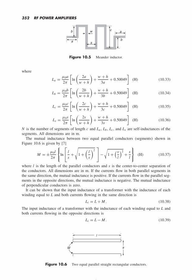
352 RF POWER AMPLIFIERS
a
b w
s
c a
b
Figure 10.5 Meander inductor.
where
La = µ0a
2π
[ln
(2a
w + h
)+ w + h
3a+ 0.50049
](H) (10.33)
Lb = µ0b
2π
[ln
(2b
w + h
)+ w + h
3b+ 0.50049
](H) (10.34)
Lc = µ0c
2π
[ln
(2c
w + h
)+ w + h
3c+ 0.50049
](H) (10.35)
Ls = µ0s
2π
[ln
(2s
w + h
)+ w + h
3s+ 0.50049
](H) (10.36)
N is the number of segments of length c and La , Lb , Lc , and Ls are self-inductances of thesegments. All dimensions are in m.
The mutual inductance between two equal parallel conductors (segments) shown inFigure 10.6 is given by [7]
M = ±µ0l
2π
ln
l
s+√
1 +(
l
s
)2−
√1 +
( s
l
)2 + s
l
(H) (10.37)
where l is the length of the parallel conductors and s is the center-to-center separation ofthe conductors. All dimensions are in m. If the currents flow in both parallel segments inthe same direction, the mutual inductance is positive. If the currents flow in the parallel seg-ments in the opposite directions, the mutual inductance is negative. The mutual inductanceof perpendicular conductors is zero.
It can be shown that the input inductance of a transformer with the inductance of eachwinding equal to L and both currents flowing in the same direction is
Li = L + M . (10.38)
The input inductance of a transformer with the inductance of each winding equal to L andboth currents flowing in the opposite directions is
Li = L − M . (10.39)
l
sM
Figure 10.6 Two equal parallel straight rectangular conductors.

INTEGRATED INDUCTORS 353
The total inductance of the meander inductor is the sum of the self-inductances of allsegments and the positive and negative mutual inductances.
The monomial equation for the total inductance of the meander inductor is given by [44]
L = 0.00266a0.0603h0.4429N 0.954s0.606w−0.173 (nH). (10.40)
where a = c/2. All dimensions are in µm. The accuracy of this equation is better than12 %.
Example 10.4
Calculate the inductance of a meander inductor with N = 5, w = 40 µm, s = 40 µm, a =40 µm, h = 100 µm, and µr = 1.
Solution. The inductance of the trace is
L = 0.00266a0.0603h0.4429N 0.954s0.606w−0.173
= 0.00266 × 400.06031000.442950.954400.60640−0.173 = 0.585 nH. (10.41)
10.6 Inductance of Straight Round Conductor
The inductance of a round straight inductor of length l and conductor radius a , whenthe effects of nearby conductors (including the return current) and the skin effect can beneglected, is given by [7]
L = µ0l
2π
[ln
(2l
a
)+ a
l− 3
4
](H) (10.42)
where the dimensions are in m. This equation can be simplified to the form
L = 0.0002l
[ln
(2l
a
)+ a
l− 0.75
](nH) (10.43)
where the dimensions are in µm.Another expression for a round straight conductor is
L = µl
8πfor δ > a. (10.44)
The inductance at high frequencies decreases with frequency. The high-frequency induc-tance of a round straight inductor when the skin effect cannot be neglected is given by
LHF = l
4πa
√µρ
π ffor δ < a. (10.45)
Example 10.5
Calculate the inductance of a round straight inductor with l = 2 mm, a = 0.1 mm, andµr = 1 for δ > a . Also, calculate the inductance of a copper round straight inductor witha = 0.1 mm at f = 1 GHz.

354 RF POWER AMPLIFIERS
Solution. The inductance of the round straight inductor for δ < a (low-frequency operation)is given by
L = µ0l
2π
[ln
(2l
a
)+ a
l− 0.75
](H)
= 4π × 10−7 × 2 × 10−3
2π
[ln
(2 × 2
0.1
)+ 0.1
2− 0.75
]= .1.1956 nH. (10.46)
The skin depth in copper at f = 1 GHz is
δ =√
ρ
πµof=√
1.724 × 10−8
π × 4π × 10−7 × 1 × 109= 2.089 µm. (10.47)
Since a = 0.1 mm = 100 µm, δ a . Therefore, the operation at f = 1 GHz is the high-frequency operation. The inductance of the round straight inductor at f = 1 GHz is
LHF = l
4πa
√µ0ρ
π f= 2 × 10⁻³
4π × 0.1 × 10−3
√4π × 10−7 × 1.724 × 10−8
π × 1 × 109= 4.179 pH.
(10.48)Hence,
FR = LHF
LLF= 4.179 × 10⁻¹²
1.1956 × 10−9= 3.493 × 10−3 = 1
286. (10.49)
10.7 Inductance of Circular Round Wire Loop
The inductance of a circular loop of round wire with loop radius r and wire radius a is [7]
L = µ0a
[ln
(8r
a
)− 1.75
](H). (10.50)
All dimensions are in m. The dependence of the inductance on wire radius is weak.The inductance of a round wire square loop is
L = µ0l
2π
[ln
(l
4a
)− 0.52401
](H) (10.51)
where l is the loop length and a is the wire radius. All dimensions are in m.
10.8 Inductance of Two-parallel Wire Loop
Consider a loop formed by two parallel conductors whose length is l radius is r , and thedistance between the conductors is s , where l s . The conductors carry equal currents inopposite directions. The inductance of the two-parallel wire loop is [7]
L = µ0l
π
[ln( s
r
)− s
l+ 0.25
](H). (10.52)

INTEGRATED INDUCTORS 355
10.9 Inductance of Rectangle of Round Wire
The inductance of a rectangle of round wir eof radius r with rectangle side lengths x andy is given by [7]
L = µ0
π
[x ln
(2x
a
)+ y ln
(2y
a
)+ 2
√x 2 + y2 − x arcsinh
(x
y
)
− y arcsinh(y
x
)− 1.75(x + y)
](10.53)
10.10 Inductance of Polygon Round Wire Loop
The inductance of a single-loop polygon can be approximated by [7]
L ≈ µp
2π
[ln
(2p
r
)− ln
(p2
A
)+ 0.25
](H) (10.54)
where p is the perimeter of the coil, A is the area enclosed by the coil, and a is the wireradius. All dimensions are in m. The inductance is strongly dependent on the perimeter andweakly dependent on the loop area and wire radius. Inductors enclosing the same perimeterwith similar shape have approximately the same inductance.
The inductance of a triangle is [7]
L = µ0l
2π
[ln
(l
3a
)− 1.15546
](H) (10.55)
where a is the wire radius. The inductance of a square is
L = µ0l
2π
[ln
(l
4a
)− 0.52401
](H). (10.56)
The inductance of a pentagon is
L = µ0l
2π
[ln
(l
5a
)− 0.15914
](H). (10.57)
The inductance of a hexagon is
L = µ0l
2π
[ln
(l
6a
)+ 0.09848
](H). (10.58)
The inductance of an octagon is
L = µ0l
2π
[ln
(l
8a
)+ 0.46198
](H). (10.59)
All dimensions in m.
10.11 Bondwire Inductors
Bondwire inductors are frequently used in RF ICs. Figure 10.7 shows a bondwire inductor. Itcan be regarded as a fraction of a round turn. Bondwires are often used for chip connections.

356 RF POWER AMPLIFIERS
Figure 10.7 Bondwire inductor.
The main advantage of bondwire inductors is a very small series resistance. Standardbondwires have a relatively large diameter of about 25 µm and can handle substantialcurrents with low loss. They may be placed well above any conductive planes to reduceparasitic capacitances and hence increase the self-resonant frequency fr . Typical inductancesrange from 2 to 5 nH. Since bondwires have much larger cross-sectional area than the tracesof planar spiral inductors, these inductors have lower resistances and hence a higher qualityfactor QLo , typically QLo = 20–50 at 1 GHz. These inductors may be placed well above anyconductive planes to reduce parasitic capacitances, yielding a higher self-resonant frequencyfr . The inductance of bondwire inductors is given by
L ≈ µ0l
2π
[ln
(2l
a
)− 0.75
](H) (10.60)
where l is the length of the bondwire and a is the radius of bondwire. A standard bondwireinductance with l = 1 mm gives L = 1 nH, or 1 nH/mm. The resistance is
R = l
2πaδσ(10.61)
where σ is the conductivity and δ is the skin depth. For aluminum, σ = 4 × 10⁷ S/m.The skin depth for aluminum is δAl = 2.5 µm at 1 GHz. The resistance per unit length isRAl/l ≈ 0.2 /mm at 2 GHz. The major disadvantage is low predictability. Bondwire induc-tance depends on bonding geometry and the existence of neighboring bondwires, makingaccurate prediction of the inductance value difficult. However, once the configuration fora particular inductance is known, it is rather repeatable in subsequent bondings. Com-mon bondwire metals include gold and aluminum. Gold is generally preferred because ofits higher conductivity and flexibility. This allows higher quality factor QLo with shorterphysical lengths to be bonded for a given die height.
Example 10.6
Calculate the inductance of a round bondwire inductor with l = 2 mm, a = 0.2 mm, andµr = 1 for δ > a .
Solution. The inductance of the round straight inductor for δ < a is
L ≈ µ0l
2π
[ln
(2l
a
)− 0.75
]= 4π × 10−7 × 2 × 10−3
2π
[ln
(2 × 2
0.2
)− 0.75
]= 0.8982 nH.
(10.62)

INTEGRATED INDUCTORS 357
10.12 Single-turn Planar Inductors
The self-inductance is a special case of mutual inductance. Therefore, an expression for theself-inductance of an inductor can be derived using the concept of the mutual inductance.This is demonstrated by deriving an expression for the inductance of a single-turn planarinductor.
Figure 10.8 shows a single-turn strip inductor of width w , inner radius b, and outer radiusa . The concept of mutual inductance can be used to determine a self-inductance. Considertwo circuits: a line circuit along the inner surface of the strip and a line current along theaxis (middle) of the strip. The vector magnetic potential caused by circuit 2 is
A2 = I2
∮C2
µdl24πh
. (10.63)
The integration of the vector magnetic potential A2 along circuit 1 resulting from the currentI2 in circuit 2 gives the mutual inductance between the two circuits
M = 1
I2
∮C1
A2 · dl1. (10.64)
Hence, the mutual inductance of two conductors is given by
M = µ
4π
∮C1
∮C2
dl1 · dl2h
. (10.65)
From geometrical consideration and the following substitution
θ = π − 2φ (10.66)
we have
dl1 = |dl1| = adθ = −2adφ (10.67)
yielding
dl1 · dl2 = dl1 dl2 cos θ = 2a cos 2φdl2dφ (10.68)
dθ
θ
dl1
dl2
h
a
b
w
Figure 10.8 Single-turn planar inductor.

358 RF POWER AMPLIFIERS
and
h =√
(a cos θ − b)2 + (a sin θ )2 =√
a2 + b2 − 2ab cos θ =√
a2 + b2 + 2ab cos 2φ
=√
a2 + b2 + 2ab(1 − 2 sin2 φ) =√
(a + b)2 − 4ab sin2 φ = (a + b)√
1 − k 2 sin2 φ
(10.69)where
k 2 = 4ab
(a + b)2= 1 − (a − b)2
(a + b)2. (10.70)
Also, ∮dl2 = 2πb. (10.71)
The mutual inductance is
M = µ
4π
∮dl2
∫ 2π
0
a cos θ dθ√a2 + b2 − 2ab cos θ
= 2µab
a + b
∫ π/2
0
(2 sin2 φ − 1) dφ√1 − k 2 sin2 φ
= µ√
abk∫ π/2
0
(2 sin2 φ − 1) dφ√1 − k 2 sin2 φ
= µ√
ab
[(2
k− k
)K (k ) − 2
kE (k )
](10.72)
where the complete elliptic integrals are
E (k ) =∫ π/2
0
√1 − k 2 sin2 φ dφ (10.73)
and
K (k ) =∫ π/2
0
dφ√1 − k 2 sin2 φ
. (10.74)
The width of the strip is
w = a − b (10.75)
resulting in
a + b = 2a − w (10.76)
ab = a(a − w ) = a2(
1 − w
a
)(10.77)
and
k 2 = 1 − w 2
(2a − w )2. (10.78)
If w/a 1, k ≈ 1, E (k ) ≈ 1,
k 2 = 1 − w 2
4a2(
1 − w
2a
)2 ≈ 1 − w 2
4a2(10.79)
and
K (k ) ≈ ln4√
1 − k 2≈ ln
4√1 −
(1 − w 2
4a2
) = ln
(8a
w
). (10.80)

INTEGRATED INDUCTORS 359
Hence, the self-inductance of a single-turn inductor is given by
L ≈ µa
[ln
(8a
w
)− 2
]= µl
2π
[ln
(8a
w
)− 2
]for a w (10.81)
where l = 2πa .
Example 10.7
Calculate the inductance of a single-turn round planar inductor with a = 100 µm, w = 1 µm,and µr = 1 for δ > a .
Solution. The inductance of the single-turn round planar inductor for δ < a is
L ≈ µa
[ln
(8a
w
)− 2
]= 4π × 10−7 × 100 × 10−6
[ln
(8 × 100
1
)− 2
]= 0.58868 nH.
(10.82)
10.13 Inductance of Planar Square Loop
The self-inductance of a square coil made of rectangular wire of length l w and widthw is
L ≈ µ0l
π
[arcsinh
(l
2w
)− 1
][H]. (10.83)
Both l and w are in m.
10.14 Planar Spiral Inductors
10.14.1 Geometries of Planar Spiral Inductors
Planar spiral inductors are the most widely used RF IC inductors. Figure 10.9 shows square,octagonal, hexagonal, and circular planar spiral inductors. A planar spiral inductor consistsof a low-resistivity metal trace (aluminum, copper, gold, or silver), silicon dioxide SiO2 ofthickness tox , and a silicon substrate, as shown in Figure 10.10. A metal layer embeddedin silicon dioxide is used to form the metal spiral. The topmost metal layer is usually thethickest and thus most conductive. In addition, a larger distance of the topmost metal layerto the substrate reduces the parasitic capacitance C = εAm/tox , increasing the self-resonantfrequency fr = 1/(2π
√LC ) where Am is the metal trace area. The substrate is a thick
silicon (Si), gallium arsenide (GaAs), or silicon germanium (SiGe) layer of thickness ofthe order of 500–700 µm. The thin silicon dioxide SiO2 of thickness 0.4–3 µm is used toisolate the metal strips of the inductor from the silicon substrate. The outer end of the spiralis connected directly to a port. The connection of the innermost turn is made through anunderpass by another metal layer or via an air bridge. The whole structure is connectedto pads and surrounded by a ground plane. Commonly used shapes of spiral inductorsare square, rectangular, hexagonal, octagonal, and circular. Hexagonal and octagonal spiral

360 RF POWER AMPLIFIERS
(a) (b)
(c) (d)
d
d
d
d
D D
D D
w
s
Figure 10.9 Planar spiral integrated inductors. (a) Square inductor. (b) Hexagonal inductor.(c) Octagonal inductor. (d) Circular inductor.
D
d
w
s
tuoxtox
tsiSilicon substrate
Figure 10.10 Cross-section of a planar RF IC inductor.

INTEGRATED INDUCTORS 361
inductors generally have less inductance and less series resistance per turn as compared tosquare spirals. Since the hexagonal and octagonal structures occupy larger chip aream theyare rarely used. A planar spiral integrated inductor can only be fabricated with technologieshaving two or more metal layers because the inner connection requires a metal layer differentthan that used for the spiral to connect the inside turn of the coil to outside. Squareinductor shapes are the most compatible with IC layout tools. They are easily designedwith Manhattan style physical layout tools, such as MAGIC. Hexagonal, octagonal, andhigher-order polygon spiral inductors have higher quality factor QLo than square spirals.The parameters of interest for integrated inductors are the inductance Ls , the quality factorQLo , and the self-resonant frequency (SRF) fr . The typical inductances are the range from1 to 30 nH, the typical quality factors are from 5 to 20, and the typical self-resonantfrequencies are from 2 to 20 GHz. The geometrical parameters of an inductor are thenumber of turns N , the metal strip width w , the metal strip height h , the turn-to-turn spaces , the inner diameter d , the outer diameter D , the thickness of the silicon substrate tSi ,the thickness of the oxide layer tox , and the thickness of oxide between the metal stripand the underpass tuox . The typical metal strip width w is 30 µm, the typical turn-to-turnspacing s is 20 µm, and the typical metal strip sheet resistance is Rsheet = ρ/h = 0.03 to0.1 per square. IC inductors require a lot of chip area. Therefore, practical IC inductorshave small inductances, typically L ≤ 10 nH, but they can be as high as 30 nH. The typicalinductor size is from 130 × 130 µm to 1000 × 1000 µm. The inductor area is A = D2. Thetopmost metal layer is usually used for construction of IC inductors because it is the thickestand thus has the lowest resistance. In addition, the distance from the topmost layer to thesubstrate is the largest, reducing the parasitic capacitances. The preferred metalization forintegrated inductors is a low-resistivity, inert metal, such as gold. Other low-resistivitymetals such as silver and copper do not offer the same level of resistance to atmosphericsulfur and moisture. Platinum, another noble metal, is two times more expensive than goldand has higher resistivity. The thickness of the metal h should be higher than 2δ one skindepth δ on the top of the trace and one skin depth on the bottom. The direction of themagnetic flux is perpendicular to the substrate. The magnetic field penetrates the substrate,inducing eddy currents. A high substrate conductivity tends to lower the inductor qualityfactor QLo . The optimization of the spiral geometry and the metal trace width leads tominimization of the trace ohmic resistance and the substrate capacitance. To reduce powerlosses in the substrate, the substrate can be made of high resistive silicon oxide such assilicon-on-insultaor (SOI), thick dielectric layers, or thick and multilayer conductor lines.
10.14.2 Inductance of Square Planar Inductors
Several expressions have been developed to estimate RF spiral inductances. In general, theinductance of planar inductors L increases when the number of turns N and the area of aninductor A increase.
The inductance of a single loop of area A and any shape (e.g., circular, square, rectangular,hexagonal, or octagonal) is given by
L ≈ µ0
√πA. (10.84)
Hence, the inductance of a single-turn round inductor of radius r is
L ≈ πµ0r = 4π2 × 10⁻⁷r = 4 × 10⁻⁶r (H). (10.85)
For example, L = 4 nH for r = 1 mm.

362 RF POWER AMPLIFIERS
The inductance of an arbitrary planar spiral inductor with N turns, often used in ICs, isgiven by
L ≈ πµ0rN 2 = 4π2 × 10⁻⁷rN 2 = 4 × 10⁻⁶rN 2 (H) (10.86)
where N is the number of turns and r is the spiral radius.
Bryan’s Formula
The inductance of the square planar spiral inductor is given by an empirical Bryan’sequation [7]
L = 6.025 × 10⁻⁷(D + d )N53 ln
[4
(D + d
D − d
)](H) (10.87)
where the outermost diameter is
D = d + 2Nw + 2(N − 1)s . (10.88)
N is the number of turns, and D and d are the outermost and innermost diameters of theinductor in m, respectively.
Example 10.8
Calculate the inductance of a square planar spiral inductor with N = 5, d = 60 µm, w =30 µm, s = 20 µm, and µr = 1 for δ > h . Use Bryan’s formula.
Solution. The outermost diameter is
D = d + 2Nw + 2(N − 1)s = 60 + 2 × 5 × 30 + 2 × (5 − 1) × 20 = 520 µm. (10.89)
The inductance of the round planar inductor for δ < h is
L = 6.025 × 10⁻⁷(D + d )N53 ln
[4
(D + d
D − d
)](H)
= 6.025 × 10⁻⁷(520 + 60) × 10−6 × 553 ln
[4
(520 + 60
520 − 60
)]= 8.266 nH. (10.90)
Wheeler’s Formula
The inductance of a square spiral inductor is given by modified Wheeler’s formula [3, 32]
L = 1.17µ0N 2 D + d
1 + 2.75D − d
D + d
(H) (10.91)
whereD = d + 2Nw + 2(N − 1)s . (10.92)
All dimensions are in m.
Example 10.9
Calculate the inductance of a square planar spiral inductor with N = 5, d = 60 µm, w =30 µm, s = 20 µm, and µr = 1 for δ > h . Use Wheeler’s formula.

INTEGRATED INDUCTORS 363
Solution. The outermost diameter is
D = d + 2Nw + 2(N − 1)s = 60 + 2 × 5 × 30 + 2 × (5 − 1) × 20 = 520 µm. (10.93)
The inductance of the square planar inductor for δ < h is
L = 1.17µ0N 2 D + d
1 + 2.75D − d
D + d
(H)
= 1.17 × 4π × 10−7 × 52 × (520 + 60) × 10−6
1 + 2.75 × 520 − 60
520 + 60
= 6.7 nH. (10.94)
Greenhouse Formula
The inductance of spiral inductors is given by Greenhouse’s equation [13]
L = 10−9DN 2
180
[log
(D
4.75(w + h)
)+ 5
]+ 1.76(w + h)
D+ 7.312
(nH). (10.95)
All dimensions are in m.
Example 10.10
Calculate the inductance of a square planar spiral inductor with N = 5, d = 60 µm, w =30 µm, s = 20 µm, h = 20 µm, and µr = 1 for δ > h . Use Greenhouse’s formula.
Solution. The outermost diameter is
D = d + 2Nw + 2(N − 1)s = 60 + 2 × 5 × 30 + 2 × (5 − 1) × 20 = 520 µm. (10.96)
The inductance of the single-turn round planar inductor for δ < h is
L = 10−9DN 2
180
[log
(D
4.75(w + h)
)+ 5
]+ 1.76(w + h)
D+ 7.312
(nH)
= 10−9 × 520 × 52
180
[log
(520
4.75(30 + 20)
)+ 5
]+ 1.76(30 + 20)
520+ 7.312
= 12.59 nH. (10.97)
Grover’s Formula
The inductance of a square or rectangular spiral planar inductor with a rectangular cross-section of the trace is expressed as [7, 30]
L = µ0l
2π
[ln
(2l
w + h
)+ w + h
3l+ 0.50049
](H) (10.98)
where the length of the metal trace is
l = 2(D + w ) + 2N (2N − 1)(w + s) (10.99)

364 RF POWER AMPLIFIERS
the outer diameter is
D = d + 2Nw + 2(N − 1)s (10.100)
and h is the metal trace height. All dimensions l , w , s , and h are in m. This equation isidentical to that for a straight trace inductor. It accounts for the self-inductance only andneglects mutual inductances between the traces.
Example 10.11
Calculate the inductance of a square planar spiral inductor with N = 5, d = 60 µm, w =30 µm, s = 20 µm, h = 20 µm, and µr = 1 for δ > h . Use Grover’s formula.
Solution. The outer diameter is
D = d + 2Nw + 2(N − 1)s = 60 + 2 × 5 × 30 + 2 × (5 − 1) × 20 = 520 µm. (10.101)
The length of the metal trace is
l = 2(D + w ) + 2N (2N − 1)(w + s) = 2(520 + 30) + 2 × 5(2 × 5 − 1)(30 + 20)
= 5600 µm. (10.102)
The inductance of the square spiral planar inductor for δ < h is
L = µ0l
2π
[ln
(2l
w + h
)+ w + h
3l+ 0.50049
](H)
= 4π × 10−7 × 5600 × 10−6
2π
[ln
(2 × 5600
30 + 20
)+ (30 + 20)
3 × 5600+ 0.50049
]= 6.608 nH. (10.103)
Rosa’s Formula
The equation for the inductance of square planar spiral inductors is expressed as [1, 8, 32]
L = 0.3175µN 2 (D + d)
ln
[2.07(D + d )
D − d
]+ 0.18(D − d )
D + d+ 0.13
(D − d
D + d
)2
(H).
(10.104)All dimensions are in m.
Example 10.12
Calculate the inductance of a square planar spiral inductor with N = 5, d = 60 µm, w =30 µm, s = 20 µm, h = 20 µm, and µr = 1 for δ > h . Use Rosa’s formula.
Solution. The outer diameter is
D = d + 2Nw + 2(N − 1)s = 60 + 2 × 5 × 30 + 2 × (5 − 1) × 20 = 520 µm. (10.105)

INTEGRATED INDUCTORS 365
The inductance of the square spiral planar inductor for δ < h is
L = 0.3175µ0N 2 (D + d)
ln
[2.07(D + d )
D − d
]+ 0.18(D − d )
D + d+ 0.13
(D − d
D + d
)2
= 0.3175 × 4π × 10−7 × 52 (520 + 60) × 10−6
×
ln
[2.07(520 + 60)
520 − 60
]+ 0.18(520 − 60)
520 + 60+ 0.13
(520 − 60
520 + 60
)2
= 6.849 nH. (10.106)
Cranin’s Formula
An empirical expression for the inductance of spiral planar inductors that has less than10 % error for inductors in the range from 5 to 50 nH is given by [21]
L ≈ 1.3 × 10⁻⁷ A5/3m
A1/6tot w 1.75(w + s)0.25
(nH) (10.107)
where Am is the metal area, Atot is the total inductor area, w is the metal trace width, ands is the spacing between metal traces. All dimensions are in m.
Example 10.13
Calculate the inductance of a square planar spiral inductor with N = 5, d = 60 µm, w =30 µm, s = 20 µm, h = 20 µm, and µr = 1 for δ > h . Use Cranin’s formula.
Solution. The outer diameter is
D = d + 2Nw + 2(N − 1)s = 60 + 2 × 5 × 30 + 2 × (5 − 1) × 20 = 520 µm. (10.108)
The length of the metal trace is
l = 2(D + w ) + 2N (2N − 1)(w + s) = 2(520 + 30) + 2 × 5(2 × 5 − 1)(30 + 20)
= 5600 µm. (10.109)
Hence, the total area of the inductor is
Atot = D2 = (520 × 10−6)2 = 0.2704 × 10⁻⁶ m2. (10.110)
The metal area is
Am = wl = 30 × 10−6 × 5600 × 10−6 = 0.168 × 10⁻⁶ m2 (10.111)
The inductance of the square spiral planar inductor for δ < h is
L ≈ 1.3 × 10⁻⁷ A5/3m
A1/6tot w 1.75(w + s)0.25
(H)
= 1.3 × 10⁻⁷ (0.168 × 10⁻⁶)5/3
(0.2704 × 10⁻⁶)1/6[30 × 10−6]1.75[(30 + 20) × 10−6]0.25
= 8.0864 nH. (10.112)

366 RF POWER AMPLIFIERS
Monomial Formula
The data fitted monomial empirical expression for the inductance of the square spiralinductor is [32]
L = 0.00162D−1.21w−0.147(
D + d
2
)2.4
N 1.78s−0.03 (nH). (10.113)
All dimensions are in µm.
Example 10.14
Calculate the inductance of a square planar spiral inductor with N = 5, d = 60 µm, w =30 µm, s = 20 µm, h = 20 µm, and µr = 1 for δ > h . Use the monomial formula.
Solution. The outer diameter is
D = d + 2Nw + 2(N − 1)s = 60 + 2 × 5 × 30 + 2 × (5 − 1) × 20 = 520 µm. (10.114)
The inductance of the square spiral planar inductor for δ < a is
L = 0.00162D−1.21w−0.147(
D + d
2
)2.4
N 1.78s−0.03 (nH)
= 0.00162 × (520)−1.21w−0.147(
520 + 60
2
)2.4
51.7820−0.03 = 6.6207 nH. (10.115)
Jenei’s Formula
The total inductance consists of the self-inductance Lself and the sum of the positive mutualinductances M + and the sum of the negative mutual inductances M −. The derivation ofan expression for the total inductance is given in [34]. The self-inductance of one straightsegment is [7]
Lself 1 = µ0lseg
2π
[ln
(2lseg
w + h
)+ 0.5
](10.116)
where lseg is the segment length, w is the metal trace width, h is the metal trace thickness.The total length of the conductor is
l = (4N + 1)d + (4Ni + 1)Ni (w + s) (10.117)
where N is the number of turns, Ni is the integer part of N , and s is the spacing betweenthe segments. The total self-inductance of a square planar inductor is equal to the sum of4N self-inductances of all the segments.
Lself = 4NLself 1 = µ0l
2π
[ln
(2l
N (w + h)
)− 0.2
]. (10.118)
The antiparallel segments contribute to negative mutual inductance M −. The sum of allinteractions is approximately equal to 4N 2 average interactions between segments of anaverage length and an average distance. The negative mutual inductance is
M − = 0.47µ0Nl
2π. (10.119)
INTEGRATED INDUCTORS 367
The positive mutual inductance is caused by interactions between parallel segments on thesame side of a square. The average distance is
b = (w + s)(3N − 2Ni − 1)(Ni + 1)
3(2N − Ni − 1). (10.120)
For Ni = N ,
b = (w + s)(N + 1)
3. (10.121)
The total positive mutual inductance is
M + = µ0l (N − 1)
2π
ln
√
1 +(
l
4Nb
)2
+ l
4Nb
−
√1 +
(4Nb
l
)2
+ 4Nb
l
.
(10.122)The inductance of a square planar inductors is
L = Lself + M − + M +
= µ0l
2π
⟨ln
[l
N (w + h)
]− 0.2 − 0.47N
+ (N − 1)
ln
√
1 +(
l
4Nb
)2
+ l
4Nb
−
√1 +
(4Nb
l
)2
+ 4Nb
l
⟩. (10.123)
All dimensions are in m.
Example 10.15
Calculate the inductance of a square planar spiral inductor with N = Ni = 5, d = 60 µm,w = 30 µm, s = 20 µm, h = 20 µm, and µr = 1 for δ > h . Use Jenei’s formula.
Solution. The total length of the conductor is
l = (4N + 1)d + (4Ni + 1)Ni (w + s)
= (4 × 5 + 1) × 60 × 10−6 + (4 × 5 + 1)5(30 + 20) × 10−6
= 6500 µm. (10.124)
The average distance is
b = (w + s)(3N − 2Ni − 1)(Ni + 1)
3(2N − Ni − 1)
= (30 + 20) × 10−6 (3 × 5 − 2 × 5 − 1)(5 + 1)
3(2 × 5 − 5 − 1)= 100 µm. (10.125)
The inductance of the square spiral planar inductor for δ < h is
L = µ0l
2π
⟨ln
[l
N (w + h)
]− 0.2 − 0.47N
+ (N − 1)
ln
√
1 +(
l
4Nb
)2
+ l
4Nb
−
√1 +
(4Nb
l
)2
+ 4Nb
l
⟩
368 RF POWER AMPLIFIERS
= 4π × 10−7 × 6500 × 10−6
2π
⟨ln
[6500
5(30 + 20)
]− 0.2 − 0.47 × 5 + (5 − 1)
×
ln
√
1 +(
6500
4 × 5 × 100
)2
+ 6500
4 × 5 × 100
−√
1 +(
4 × 5 × 100
6500
)2
+ 4 × 5 × 100
6500
⟩
= 6.95 nH. (10.126)
Dill’s Formula
The inductance of a square planar inductor is [9]
L = 8.5 × 10⁻¹⁰N 5/3 (H). (10.127)
For N = 5, L = 12.427 nH.
Terman’s Formula
The inductance of a square planar spiral single-turn inductor is
L = 18.4173 × 10⁻⁴D
[log
(0.7874 × 10⁻⁴D2
w + h
)− log(0.95048 × 10⁻⁴D)
]
+ 10−4 × [7.3137D + 1.788(w + h)] (nH). (10.128)
All dimensions are in µm.The inductance of a square planar spiral multiple-turn inductor is
L = 18.4173 × 10⁻⁴DN 2[
log
(0.7874 × 10⁻⁴D2
w + h
)− log(0.95048 × 10⁻⁴D)
]
+ 8 × 10⁻⁴N 2[0.914D + 0.2235(w + h)] (nH). (10.129)
where the outer diameter is
D = d + 2Nw + 2(N − 1)s . (10.130)
All dimensions are in m.
Example 10.16
Calculate the inductance of a square planar spiral inductor with N = 5, D = 520 µm, w =30 µm, h = 20 µm, and µr = 1 for δ > h . Use Terman’s formula.
Solution. The inductance of a square planar spiral multiple-turn inductor is
L = 18.4173 × 10⁻⁴DN 2[
log
(0.7874 × 10⁻⁴D2
w + h
)− log(0.95048 × 10⁻⁴D)
]
+ 8 × 10⁻⁴N 2[0.914D + 0.2235(w + h)] (nH)

INTEGRATED INDUCTORS 369
= 18.4173 × 10−4 × 520 × 52[
log
(0.7874 × 10−4 × 5202
30 + 20
)
− log(0.95048 × 10−4 × 520)
]
+ 8 × 10−452[0.914 × 520 + 0.2235(30 + 20)]
= 32.123 (nH). (10.131)
Rosa’s, Wheeler’s, Grover’s, Bryan’s, Jenei’s, and monomial formulas give similar valuesof inductance. Geenhouse’s, Cranin’s, Terman’s formulas give higher values of inductancethan those calculated from the former group of formulas.
10.14.3 Inductance of Hexagonal Spiral Inductors
Wheeler’s Formula
The inductance of a hexagonal spiral inductor is given by modified Wheeler’s formula[3, 32]
L = 1.165µ0N 2 D + d
1 + 3.82D − d
D + d
(H) (10.132)
whereD = d + 2Nw + 2(N − 1)s . (10.133)
All dimensions are in m.
Rosa’s Formula
The equation for the inductance of hexagonal planar spiral inductors is expressed as [1, 8,32]
L = 0.2725µN 2 (D + d)
ln
[2.23(D + d )
D − d
]+ 0.17
(D − d
D + d
)2
(H). (10.134)
All dimensions are in m.
Example 10.17
Calculate the inductance of a hexagonal planar spiral inductor with N = 5, d = 60 µm,w = 30 µm, s = 20 µm, h = 20 µm, and µr = 1 for δ > h . Use Rosa’s formula.
Solution. The outer diameter is
D = d + 2Nw + 2(N − 1)s = 60 + 2 × 5 × 30 + 2 × (5 − 1) × 20 = 520 µm. (10.135)
The inductance of the square spiral planar inductor for δ < h is
L = 0.2725µN 2 (D + d)
ln
[2.23(D + d )
D − d
]+ 0.17
(D − d
D + d
)2
(H).

370 RF POWER AMPLIFIERS
= 0.2725 × 4π × 10−7 × 52 (520 + 60) × 10−6
×
ln
[2.23(520 + 60)
520 − 60
]+ 0.17
(520 − 60
520 + 60
)2
= 5.6641 nH. (10.136)
Grover’s Formula
The inductance of a hexagonal planar inductor is [7]
L = 2µl
π
[(l
6r
)+ 0.09848
](H). (10.137)
All dimensions are in µm.
Monomial Formula
The data fitted monomial empirical expression for the inductance of the hexagonal spiralinductor is [32]
L = 0.00128D−1.24w−0.174(
D + d
2
)2.47
N 1.77s−0.049 (nH). (10.138)
All dimensions are in µm.
10.14.4 Inductance of Octagonal Spiral Inductors
Wheeler’s Formula
The inductance of an octagonal spiral inductor is given by a modified Wheeler’s formula[3, 32]
L = 1.125µ0N 2 D + d
1 + 3.55D − d
D + d
(H) (10.139)
where
D = d + 2Nw + 2(N − 1)s . (10.140)
All dimensions are in m.
Rosa’s Formula
. The inductance of an octagonal planar spiral inductors is expressed as [1, 8, 32]
L = 0.2675µN 2 (D + d)
ln
[2.29(D + d )
D − d
]+ 0.19
(D − d
D + d
)2
(H). (10.141)
All dimensions are in m.
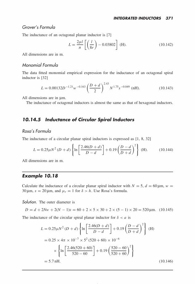
INTEGRATED INDUCTORS 371
Grover’s Formula
The inductance of an octagonal planar inductor is [7]
L = 2µl
π
[(l
8r
)− 0.03802
](H). (10.142)
All dimensions are in m.
Monomial Formula
The data fitted monomial empirical expression for the inductance of an octagonal spiralinductor is [32]
L = 0.00132D−1.21w−0.163(
D + d
2
)2.43
N 1.75s−0.049 (nH). (10.143)
All dimensions are in µm.The inductance of octagonal inductors is almost the same as that of hexagonal inductors.
10.14.5 Inductance of Circular Spiral Inductors
Rosa’s Formula
The inductance of a circular planar spiral inductors is expressed as [1, 8, 32]
L = 0.25µN 2 (D + d)
ln
[2.46(D + d )
D − d
]+ 0.19
(D − d
D + d
)2
(H). (10.144)
All dimensions are in m.
Example 10.18
Calculate the inductance of a circular planar spiral inductor with N = 5, d = 60 µm, w =30 µm, s = 20 µm, and µr = 1 for δ > h . Use Rosa’s formula.
Solution. The outer diameter is
D = d + 2Nw + 2(N − 1)s = 60 + 2 × 5 × 30 + 2 × (5 − 1) × 20 = 520 µm. (10.145)
The inductance of the circular spiral planar inductor for δ < a is
L = 0.25µN 2 (D + d)
ln
[2.46(D + d )
D − d
]+ 0.19
(D − d
D + d
)2
(H)
= 0.25 × 4π × 10−7 × 52 (520 + 60) × 10−6
×
ln
[2.46(520 + 60)
520 − 60
]+ 0.19
(520 − 60
520 + 60
)2
= 5.7 nH. (10.146)

372 RF POWER AMPLIFIERS
Wheeler’s Formula
The inductance of a circular planar inductor is [2]
L = 31.33µN 2 a2
8a + 11h(H). (10.147)
All dimensions are in m.
Schieber Formula
The inductance of a circular planar inductor is [15]
L = 0.874π × 10−5DN 2(H). (10.148)
All dimensions are in m.Spiral IC inductors have high parasitic resistances and high shunt capacitances, resulting
in a low QLo and low self-resonant frequencies. It is difficult to achieve QLo > 10 and frgreater than a few GHz for planar inductors due to the loss in the substrate and metalization.The RF MEMS technology has the potential to improve the performance of RF IC inductorsby removing the substrate under the planar spiral via top-side etching, which decouples theRF IC inductor performance from substrate characteristics.
10.15 Multimetal Spiral Inductors
Multimetal planar spiral inductors (called stacked inductors) are also used to achieve com-pact high-inductance magnetic devices. A double layer spiral inductor can be implementedusing metal 1 and metal 2 layers, as shown in Figure 10.11 [39, 40]. An equivalent circuitof a two-layer inductor is shown in Figure 10.12.
The impedance of a two-layer inductor is given by
Z = jω(L1 + L2 + 2M ) = jω(L1 + L2 + 2k√
L1L2) ≈ jω(L1 + L2 + 2√
L1L2) (10.149)
where the coupling coefficient k ≈ 1. If both inductors are equal,
Z ≈ jω(L + L + 2L) = jω(4L) = jωLs . (10.150)
Metal 2
Metal 1
Metal around ring
Ground shield withn-type diffusion
Figure 10.11 Multimetal spiral inductor that uses metal 1 and metal 2.

INTEGRATED INDUCTORS 373
M
L2
L1
Ls
Figure 10.12 Equivalent circuit of two-layer inductor.
Thus, the total inductance Ls for a two-layer inductor increases nearly four times due tomutual inductance. For an m-layer inductor, the total inductance is increased by a factorof m2 as compared to a self-inductance of a single-layer spiral inductor. Modern CMOStechnologies provide more than five metal layers and stocking inductors or transformersgives large inductances in a small chip area.
A patterned ground shield reduces eddy currents. Many RF IC designs incorporate severalinductors on the same die. Since these structures are physically large, substrate couplingcan cause significant problems, such as feedback and oscillations.
The spiral inductors have several drawbacks. First, the size is large compared with otherinductors for the same number of turns N . Second, the spiral inductor requires a lead wireto connect the inside end of the coil to the outside, which introduces a capacitance betweenthe conductor and the lead wire, and this capacitance is the dominant component of theoverall stray capacitance. Third, the direction of the magnetic flux is perpendicular to thesubstrate, which can interfere with the underlying circuit. Fourth, the quality factor is verylow. Fifth, the self-resonant frequency is low.
10.16 Planar Transformers
Monolithic transformers are required in many RF designs. The principle of planar trans-formers relies on lateral magnetic coupling. They can be used as narrowband or widebandtransformers. An interleaved planar spiral transformer is shown in Figure 10.13. The cou-pling coefficient of theses transformers is k ≈ 0.7. Figure 10.14 shows a planar spiraltransformer, in which the turns ratio n = Np : Ns is not equal to 1. The coupling coefficient kis low in this transformer, typically k = 0.4. Stacked transformers use multiple metal layers.
Figure 10.13 Interleaved planar spiral transformer.

374 RF POWER AMPLIFIERS
Figure 10.14 Planar spiral transformer in which the turns ratio n = Np : Ns is not equal to 1.
10.17 MEMS Inductors
Microelectromechanical system (MEMS) technology can improve the performance of inte-grated inductors MEMS inductors usually are solenoids fabricated using surface microma-chining techniques and polymer/metal multilayer process techniques. Figure 10.15 showan integrated solenoid inductor [29]. These inductors may have air cores or electroplatedNi-Fe Permalloy cores. The winding is made up of electroplated copper layers. There is anair gap between the metal winding and the substrate. This geometry gives small inductorsize, low stray capacitance CS , high self-resonant frequency fr , low power loss, and highquality factor. However, it requires a 2D design approach.
The magnetic field intensity inside the solenoid is uniform and given by
B = µNI
lc(10.151)
where lc is the length of the core and N is the number of turns. The magnetic flux is
φ = AcB = µNIAc
lc(10.152)
where Ac is the cross-sectional area of the core. The magnetic linkage is
λ = N φ = µN 2IAc
lc. (10.153)
Air-gap
Substrate
Figure 10.15 Integrated MEMS solenoid inductor [29].

INTEGRATED INDUCTORS 375
0 0.2 0.4 0.6 0.8 1 1.2 1.40.4
0.5
0.6
0.7
0.8
0.9
1
r/ lc
L/L
∞
Figure 10.16 Ratio L/L∞ versus r/lc .
The inductance of the infinitely long MEMS solenoid inductor is given by
L = λ
I= µN 2Ac
lc. (10.154)
The inductance of a short solenoid is lower that of an infinitely long one. The inductance ofa round solenoid of radius r and length lc can be determined from Wheeler’s equation [2]
L = L∞
1 + 0.9r
lc
= µAcN 2
lc
(1 + 0.9
r
lc
) . (10.155)
For a square solenoid, we can use an equivalent cross-sectional area of the solenoid
A = h2 = πr2 (10.156)
yielding
r = h√π
. (10.157)
Figure 10.16 show a plot of L/L∞ as a function of r/lc .
Example 10.19
Calculate the inductance of a MEMS solenoid made of N = 10 turns of square wire withthickness h = 8 µm and space between the turns s = 8 µm. The solenoid has a square shapewith width w = 50 µm.

376 RF POWER AMPLIFIERS
Solution. The cross-sectional area of the MEMS solenoid is
Ac = w 2 = (50 × 10−6)2 = 25 × 10−10 m2. (10.158)
The length of the solenoid is
lc = (N − 1)(h + s) = (10 − 1)(8 + 8) × 10−6 = 144 × 10−6 m = 144 µm. (10.159)
The inductance of the solenoid is
L = µN 2Ac
lc= 4π × 10−7 × 102 × 25 × 10−10
144 × 10−6= 2.182 nH. (10.160)
Brooks Inductor
The maximum inductance with a given length of wire is obtained for a/c = 3/2 andb = c, where a is the coil mean radius, b is the coil axial thickness, and c is the coil radialthickness. The inductance in this case is [16, 17]
L = 1.353µaN 2. (10.161)
10.18 Inductance of Coaxial Cable
The inductance of a coaxial cable is
L = µl
2πln
(b
a
)(10.162)
where a is the inner radius of the dielectric, b is the outer radius of the dielectric, and l isthe length of the coaxial cable.
10.19 Inductance of Two-wire Transmission Line
The inductance of a two-parallel-wire transmission line is
L = µl
π
ln
(d
2a
)+√(
d
2a
)2
− 1
(10.163)
where a is the of the wires and d is the distance between the centers of the wires, and l isthe length of the transmission line.
10.20 Eddy Currents in Integrated Inductors
The performance degradation of planar spiral inductors is caused by the following effects:
(1) trace resistance due to its conductivity (σ < ∞);
(2) eddy-current losses due to magnetic field penetration into the substrate and adjacenttraces;

INTEGRATED INDUCTORS 377
Figure 10.17 RF IC inductor with a variable trace width.
(3) substrate ohmic losses;
(4) capacitance formed by metal trace, silicon oxide, and substrate.
When a time-varying voltage is applied between the terminals of the inductor, a time-varyingcurrent flowing along the inductor conductor induces a magnetic field. The magnetic fieldinduces eddy current in the substrate.
A broken guard ring made up of n+ or p+ diffusion regions surrounding the coil andconnected to ground is often used. The purpose of the guard ring is to provide a low-impedance path to ground for currents induced in the substrate, reducing the substrate lossand increasing the inductor quality factor.
Another method for reducing the loss in the substrate is to insert a high-conductivityground shield between the spiral and the substrate. The ground shield is patterned withslots to reduce the paths for eddy currents.
If an n-well is fabricated beneath the oxide, the p-substrate and the n-well form apn junction. If this junction is reverse biased, it represent a capacitance CJ . The oxidecapacitance Cox and the junction capacitance CJ are connected in series, reducing the totalcapacitance. Therefore, the current flowing from the metal trace to the substrate is reduced,reducing substrate loss and improving the quality factor.
Various structures may be used to block eddy currents. Eddy currents flow in pathsaround the axis of the spiral. This can be accomplished by inserting narrow strips of n+regions perpendicular to the eddy current flow to create blocking pn junctions.
The magnetic field reaches the maximum value near the axis of the spiral inductor. Thecurrent density is higher in the outer turns than that in ihe inner turns. Therefore, the seriesresistance and the power loss can be reduced if the outer turns are wider than the innerturns, as illustrated in Figure 10.17. Also, the spacing between the turns can be increasedthe center of the spiral to the outer turns.
10.21 Model of RF Integrated Inductors
A two-port π -model of RF IC planar spiral inductors is shown in Figure 10.18 [25]. Thecomponents Ls , Rs , and Cs represent the inductance, resistance, and capacitance of the metaltrace. The capacitance Cox represents the metal-oxide-substrate capacitance. The compo-nents Rsi and CSi represent the resistance and capacitance of the substrate. The inductanceL is given by one of the equation given in Section 10.14. The ac resistance is given by(10.17).

378 RF POWER AMPLIFIERS
Cox Cox
LS
RSi RSiCSi CSi
RS
CS
Figure 10.18 Lumped-parameter physical model of an RF IC spiral inductors.
The shunt stray capacitance is formed by the overlap of the underpass and the spiralinductor turns. It is given by
CS = εoxNw 2
tox. (10.164)
The turn-to-turn capacitances Ctt are small even for very small spacing s between theturns because the thickness of the metal trace h is small, resulting in a small verticalarea. The lateral turn-to-turn capacitances are connected in series and therefore the equiv-alent interturn capacitance Ctt/N is small. The adjacent turns sustain a very small voltagedifference. The electric energy stored in turn-to-turn capacitances is proportional to thesquare of voltage. Also, the displacement current through the turn-to-turn capacitanceiC = Ctt dv/dt ≈ Cttv/δt is very low. Therefore, the effect of the turn-to-turn capaci-tances is negligible. The effect of the overlap capacitance is more significant because thepotential difference between the underpass and the spiral turns is higher. The stray capac-itance allows the current to flow directly from the input port to the output port withoutpassing through the inductance. The current can also flow between one terminal and thesubstrate through capacitances Cox and CSi .
The capacitance between the metal trace and the silicon substrate is
Cox = εoxA
2tox= wl
εox
2tox(10.165)
where w is the trace width, l is the trace length, A = wl is the area of the metal trace, tox isthe thickness of the silicon dioxide SiO2, and εox = 3.9ε0 is the permittivity of the silicondioxide. The typical value of tox is 1.8 × 10⁻⁸ m.
The capacitance of the substrate is
CSi ≈ wlCsub
2(10.166)
where Csub = 10−3 to 10−2 fF/µm2.The resistance representing the substrate dielectric loss is given by
RSi = 2
wlGsub(10.167)
where Gsub is the substrate conductance per unit area, typically Gsub = 10−7 S/µm2.
10.22 PCB Integrated Inductors
A printed circuit board (PCB) inductor is shown in Figure 10.19. The types of inductorsthat can be used for printed circuit boards technology are
• coreless inductors;
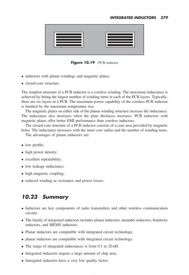
INTEGRATED INDUCTORS 379
Figure 10.19 PCB inductor
• inductors with planar windings and magnetic plates;
• closed-core structure.
The simplest structure of a PCB inductor is a coreless winding. The maximum inductance isachieved by fitting the largest number of winding turns in each of the PCB layers. Typically,there are six layers in a PCB. The maximum power capability of the coreless PCB inductoris limitted by the maximum temperature rise.
The magnetic plates on either side of the planar winding structure increase the inductance.The inductance also increases when the plate thickness increases. PCB inductors withmagnetic plates offer better EMI performance than coreless inductors.
The closed-core structure of a PCB inductor consists of a core area provided by magneticholes. The inductance increases with the inner core radius and the number of winding turns.
The advantages of planar inductors are:
• low profile;
• high power density;
• excellent repeatability;
• low leakage inductance;
• high magnetic coupling;
• reduced winding ac resistance and power losses.
10.23 Summary
• Inductors are key components of radio transmitters and other wireless communicationcircuits.
• The family of integrated inductors includes planar inductors, meander inductors, bondwireinductors, and MEMS inductors.
• Planar inductors are compatible with integrated circuit technology.
• planar inductors are compatible with integrated circuit technology.
• The range of integrated inductances is from 0.1 to 20 nH.
• Integrated inductors require a large amount of chip area.
• Intergated inductors have a very low quality factor.

380 RF POWER AMPLIFIERS
• Planar spiral RF IC inductors are the most widely used inductors.
• Meander inductors require only one metal layer.
• Meander inductors have a low inductance-to-surface area ratio.
• Planar inductors usually require two metal layers.
• Planar spiral inductors have a high inductance per unit area.
• The direction of magnetic flux is perpendicular to the substrate and therefore can interferewith the circuit.
• In square planar inductors, the total self-inductance is equal to the sum of self-inductancesof all straight segments.
• In square planar inductors, the the mutual inductance is only present between parallelsegments.
• The mutual inductance between parallel segments is positive if the currents in parallelconductors flow in the same direction.
• The mutual inductance between parallel segments is negative if the currents in parallelconductors flow in the opposite directions.
• The inductance of planar inductors is approximately proportional to the trace length l .
• An increase in the conductor width w and spacing s reduces the inductance and theresistance.
• The conductor thickness does not affect the inductance value and significantly reducesthe resistance.
• The magnetic flux of RF IC inductors penetrates the substrate, where it induces high-losseddy currents.
• Patterned ground shield can be used to reduce eddy current loss.
• MEMS solenoid inductors are more complex to fabricate than the planar spiral inductors.
• MEMS inductors have a higher quality factor than the planar integrated inductors.
• The predictability of bondwire inductors is low.
• The parasitic capacitance of integrated planar inductors can be minimized by implement-ing the spiral with the topmost metal layer, increasing the self-resonant frequency.
10.24 References
[1] E. B. Rosa, ‘Calculation of the self-inductance of single-layer coils,’ Bull. Bureau Standards,vol. 2, no. 2, pp. 161-187, 1906.
[2] H. A. Wheeler, ‘Simple inductance formulas for radio coils,’ Proc. IRE, vol. 16, no. 10, pp.1398-1400, October 1928.
[3] H. A. Wheeler, ‘Formulas for the skin effect,’ Proc. IRE, vol. 30, pp. 412-424, September 1942.[4] F. E. Terman, Radio Engineers’ Handbook, New York: McGraw-Hill, 1943.[5] R. G. Medhurst, ‘HF resistance and self-capacitance of single-layer solenoids,’ Wireless Engi-
neers, pp. 35-43, February 1947, and pp. 80-92, March 1947.[6] H. E. Bryan, ‘Printed inductors and capacitors,’ Tele-Tech and Electronic Industries, vol. 14,
no. 12, p. 68, December 1955.

INTEGRATED INDUCTORS 381
[7] F. W. Grover, Inductance Calculations: Working Formulas and Tables, Princeton, NJ: VanNostrand, 1946; reprinted by Dover Publications, New York, NY, 1962.
[8] J. C. Maxwell, A Treatise of Electricity and Magnetism, Parts III and IV, 1st Ed., 1873, 3rd Ed,1891; reprinted by Dover Publishing, New York, NY, 1954 and 1997.
[9] H. Dill, ‘Designing inductors for thin-film applications,’ Electronic Design, pp. 52-59, February17, 1964.
[10] D. Daly, S. Knight, M. Caulton, and R. Ekholdt, ‘Lumped elements in microwave integratedcircuits,’ IEEE Transactions on Microwave Theory and Techniques, vol. 15, no. 12, pp. 713-721,December 1967.
[11] J. Ebert, ‘Four terminal parameters of HF inductors’ Bull. Acad. Polon. Sci., Ser. Sci. Techn.,Bull. de l’Academie Polonaise de Sci., no. 5, 1968.
[12] R. A. Pucel, D. J. Masse, and C. P. Hartwig, ‘Losses in microstrops,’ IEEE Transactions onMicrowave Theory and Techniques, vol. 16, no. 6, pp. 342-250, June 1968.
[13] H. M. Greenhouse, ‘Design of planar rectangular microelectronic inductors,’ IEEE Transactionson Parts, Hybrids, and Packaging, vol. PHP-10, no. 2, pp. 101-109, June 1974.
[14] N. Saleh, ‘Variable microelectronic inductors,’ IEEE Transactions on Components, Hybrids, andManufacturing Technology, vol. 1, no. 1, pp. 118-124, March 1978.
[15] D. Schieber, ‘On the inductance of printed spiral coils,’ Archiv fur Elektrotechnik, vol. 68, pp.155-159, 1985.
[16] B. Brooks, ‘Design of standards on inductance, and the proposed use of model reactors in thedesign of air-core and iron-core reactors,’ Bur. Standard J. Res., pp. 289-328, vol. 7, 1931.
[17] P. Murgatroyd, ‘The Brooks inductor: A study of optimal solenoid cross-sections,’ IEE Pro-ceedings, Part B, Electric Power Applications, vol. 133, no. 5, pp. 309-314, September 1986.
[18] L. Weimer and R. H. Jansen, ‘Determination of coupling capacitance of underpasses, air bridgesand crossings in MICs and MMICS,’ Electronic Letters, vol. 23, no. 7, pp. 344-346, March1987.
[19] N. M. Nguyen and R. G. Mayer, ‘Si IC-compatible inductors and LC passive filter,’ IEEE J.Solid-State Circuits, vol. 27, no. 10, pp. 1028-1031, August 1990.
[20] P. R. Gray and R. G. Mayer, ‘Future directions in silicon IC’s for RF personal communications,’Proc. IEEE 1995 Custom Integrated Circuits Conf., May 1995, pp. 83-90.
[21] J. Craninckx and M. S. J. Steyeart, ‘A 1.8 GHz CMOS low noise voltage-controlled oscillatorwith prescalar,’ IEEE J. Solid-State Circuits, vol. 30, pp. 1474-1482, December 1995.
[22] J. R. Long and M. A. Copeland, ‘The modeling, characterization, and design of monolithicinductors for silicon RF IC’s,’ IEEE J. Solid-State Circuits, vol. 32, no. 3, pp. 357-369, May1997.
[23] J. N. Burghartz, M. Soyuer, and K. Jenkins, ‘Microwave inductors and capacitors in stan-dard multilevel interconnect silicon technology,’ IEEE Transactions on Microwave Theory andTechnique, vol. 44, no. 1, pp. 100-103, January 1996.
[24] K. B. Ashby, I. A. Koullias, W. C. Finley, J. J. Bastek, and S. Moinian, ‘High Q inductors forwireless applications in a complementary silicon bipolar process,’ IEEE J. Solid-State Circuits,vol. 31, no. 1, pp. 4-9, January 1996.
[25] C. P. Yue, C. Ryu, J. Lau, T. H. Lee, and S. S. Wong, ‘A physical model for planar spiralinductors in silicon,’ International Electron Devices Meeting Technical Digest, December 1996,pp. 155-158.
[26] C. P. Yue and S. S. Wang, ‘On-chip spiral inductors with patterned ground shields for Si-basesRF ICs,’ IEEE J. Solid-State Circuits, vol. 33, no. 5, pp. 743-752, May 1998.
[27] F. Mernyei, F. Darrer, M. Pardeon, and A. Sibrai, ‘Reducing the substrate losses of RF integratedinductors,’ IEEE Microwave and Guided Wave Letters, vol. 8. no. 9, pp. 300-3001, September1998.
[28] A. M. Niknejad and R. G. Mayer, ‘Analysis, design, and optimization of spiral inductors andtransformers for Si RF IC’s,’ IEEE J. Solid-State Circuits, vol. 33. no. 10, pp. 1470-1481,October 1998.
[29] Y.-J. Kim and M. G. Allen, ‘Integrated solenoid-type inductors for high frequency applicationsand their characteristics,’ 1998 Electronic Components and Technology Conference, 1998, pp.1249-1252.

382 RF POWER AMPLIFIERS
[30] C. P. Yue and S. S. Wong, ‘Design strategy of on-chip inductors highly integrated RF systems,’Proc. 36th Design Automation Conference, 1999, pp. 982-987.
[31] M. T. Thomson, ‘Inductance calculation techniques − Part II: Approximations and handbookmethods,’ Power Control and Intelligent Motion, pp. 1-11, December 1999.
[32] S. S. Mohan, M. Hershenson. S. P. Boyd, and T. H. Lee, ‘Simple accurate expressions forplanar spiral inductors,’ IEEE J. Solid-State Circuits, vol. 34, no. 10, pp. 1419-1424, October1999.
[33] Y. K. Koutsoyannopoulos and Y. Papananos, ‘Systematic analysis and modeling of integratedinductors and transformers in RF IC design’ IEEE Transactions on Circuits and Systems-II,Analog and Digital Signal Processing, vol. 47, no. 8, pp. 699-713, August 2000.
[34] S. Jenei, B. K. J. Nauwelaers, and S. Decoutere, ‘Physics-based closed-form inductance expres-sions for compact modeling of integrated spiral inductors,’ IEEE Journal of Solid-State Circuits,vol. 37, no. 1, pp. 77-80, January 2002.
[35] T.-S. Horng. K.-C. Peng, J.-K. Jau, and Y.-S. Tsai, ‘S -parameters formulation of quality factorfor a spiral inductor in generalized tow-port configuration,’ IEEE Transactions on MicrowaveTheory and Technique, vol. 51, no. 11, pp. 2197-2202, November 2002.
[36] J. Aguilera and R. Berenguer, Design and Test of Integrated Inductors for RF Applications,Kluwer Academic Publishers, Boston, MA, 2003.
[37] W. Y. Lin, J. Suryanarayan, J. Nath, S. Mohamed, L. P. B. Katehi, and M. B. Steer, ‘Toroidalinductors for radio-frequency integrated circuits,’ IEEE Transactions on MIcrowave Circuitsand Techniques, vol. 52, no. 2, pp. 646-651, February 2004.
[38] N. Wong, H. Hauser, T. O’Donnel, M. Brunet, P. McCloskey, and S. C. O’Mathuna, ‘Modelingof high-frequency micro-transformers,’ IEEE Trans. Magnetics, vol. 40, pp. 2014-2016, July2004.
[39] T. Suetsugu and M. K. Kazimierczuk, ‘Integration of Class DE inverter for dc-dc converteron-chip power supplies,’ IEEE International Symposium on Circuits and Systems, Kos, Greece,May 21-24, 2006, pp. 3133-3136.
[40] T. Suetsugu and M. K. Kazimierczuk, ‘Integration of Class DE synchronized dc-dc converteron-chip power supplies,’ IEEE Power Electronics Specialists Conference, Jeju, South Korea,June 21-24, 2006.
[41] W-Z. Chen, W-H. Chen, and K-C. Hsu, ‘Three-dimensional fully symmetrical inductors, trans-formers, and balun in CMOS technology,’ IEEE Trans. Circuits and Systems-I, vol. 54, no. 7,pp. 1413-1423, July 2007.
[42] A. Massarini and M. K. Kazimierczuk, ‘Self-capacitance of inductors,’ IEEE Transactions onPower Electronics, vol. 12, no. 4, pp. 671-676, July 1997.
[43] G. Grandi, M. K. Kazimierczuk, A. Massarini, and U. Reggiani, ‘Stray capacitance of single-layer solenoid air-core inductors,’ IEEE Trans. Industry Applications, vol. 35, no. 5, pp. 1162-1168, September 1999.
[44] G. Stojanovic, L. Zivanov, and M. Damjanovic, ‘Compact form of expressions for inductancecalculation of meander inductors,’ Serbian Journal of Electrical Engineering, vol. 1, no. 3, pp.57-68, November 2004.
[45] J.-T. Kuo, K.-Y. Su, T.-Y. Liu, H.-H. Chen and S.-J. Chung, ‘Analytical calculations for dcinductances of rectangular spiral inductors with finite metal thickness in the PEEC Formulation,’IEEE Microwave and Wireless Components Letters, pp. 1-3, 2006.
10.25 Review Questions
10.1 List the types of integrated inductors.
10.2 What is the range of integrated inductances?
10.3 Is it easy to achieve good performance of integrated inductors?
10.4 What kind of integrated inductors are the most widely used?

INTEGRATED INDUCTORS 383
10.5 What is the main disadvantage of planar integrated inductors?
10.6 How many metal layers are usually used in RF IC planar inductors?
10.7 What is underpass in spiral planar inductors?
10.8 What is air bridge in integrated inductors?
10.9 When is the mutual inductance between two conductors zero?
10.10 When is the mutual inductance between two conductors positive and when is itnegative?
10.11 Is the quality factor high for integrated inductors?
10.12 What is the self-resonant frequency of an inductor?
10.13 What is the main disadvantage of bondwire inductors?
10.14 What is the advantages and disadvantage of planar inductors?
10.15 What are the advantages and disadvantage of MEMS inductors?
10.16 How can eddy current losses be reduced?
10.17 What are the components of the model of planar spiral inductors?
10.26 Problems
10.1 Calculate the skin depth at f = 1 GHz for (a) copper, (b) aluminum, (c) silver, and(d) gold.
10.2 Calculate the dc resistance of a copper trace with l = 50 µm, w = 1 µm, and h =1 µm. Find the ac resistance of the trace at 10 GHz. Calculate FR .
10.3 Calculate the inductance of a straight trace with l = 100 µm, w = 1 µm, h = 1 µm,and µr = 1.
10.4 Calculate the inductance of a meander inductor with N = 10, w = 40 µm, s =40 µm, a = 40 µm, h = 100 µm, and µr = 1.
10.5 Calculate the inductance of a round straight inductor with l = 2 mm and µr = 1for δ h . Find the inductance of the above copper round straight conductor fora = 20 µm at f = 2.4 GHz.
10.6 Calculate the inductance of a bondwire with l = 1 mm and a = 1 µm.
10.7 Find the inductance of the spiral planar inductor with N = 10 and r = 100 µm.
10.8 Calculate the inductance of a square planar spiral inductor with N = 10, s = 20 µm,w = 30 µm, and d = 40 µm. Use Bryan’s formula.
10.9 Calculate the square planar spiral inductance with N = 10, s = 20 µm, w = 30 µm,and d = 40 µm. Use Wheeler’s formula.
10.10 Calculate the square planar spiral inductance with N = 15, s = 20 µm, w = 30 µm,h = 20 µm, and d = 40 µm. Use Greenhouse’s formula.
10.11 Calculate the square planar spiral inductance with N = 10, s = 20 µm, w = 30 µm,h = 20 µm, and d = 40 µm. Use Rosa’s formula.

384 RF POWER AMPLIFIERS
10.12 Calculate the square planar spiral inductance with N = 10, s = 20 µm, w = 30 µm,h = 20 µm, and d = 40 µm. Use Cranin’s formula.
10.13 Calculate the square planar spiral inductance with N = 10, s = 20 µm, w = 30 µm,h = 20 µm, and d = 40 µm. Use the monomial formula.
10.14 Calculate the square planar spiral inductance with N = Ni = 10, s = 20 µm, w =30 µm, h = 20 µm, and d = 40 µm. Use Jenei’s formula.
10.15 Calculate the square planar spiral inductance with N = 10, w = 30 µm, h = 20 µm,and D = 1000 µm. Use Terman’s formula.
10.16 Calculate the hexagonal planar spiral inductance with N = 10, s = 20 µm, w =30 µm, h = 20 µm, and d = 40 µm. Use Rosa’s formula.
10.17 Calculate the octagonal planar spiral inductance with N = 5, s = 20 µm, w = 30 µm,h = 20 µm, and d = 60 µm. Use Rosa’s formula.
10.18 Calculate the circular planar spiral inductance with N = 15, d = 40 µm, w = 30 µm,and s = 20 µm. Use Wheeler’s formula. Use Wheeler’s formula.
10.19 Calculate the inductance of a MEMS solenoid with N = 20. The thickness of thesquare wire is h = 10 µm and the separation between the turns is s = 10 µm. Thesolenoid has a square shape with w = 100 µm.

Appendices


ASPICE Model of PowerMOSFETs
Figure A.1 shows a SPICE large-signal model for n-channel enhancement MOSFETs. Itis a model for integrated MOSFETs, which can be adopted to power MOSFETs. SPICEparameters of the large-signal model of enhancement-type n-channel MOSFETs are givenin Table A.1. The diode currents are
iBD = IS(
evBDVT − 1
)(A.1)
and
iBS = IS
(e
vBSVT − 1
). (A.2)
The junction capacitances in the voltage range close to zero are
CBD = (CJ )(AD)(1 − vBD
PB
)MJ for vBD ≤ (FC )(PB) (A.3)
and
CBS = (CJ )(AS )(1 − vBS
PB
)MJ for vBS ≤ (FC )(PB) (A.4)
where CJ is the zero-bias junction capacitance per unit area, AD is the drain area, AS isthe source area, PB is the built-in potential, and MJ is the grading coefficient.
The junction capacitances in the voltage range far from zero are
CBD = (CJ )(AD)
(1 − FC )1+MJ
[1 − (1 + MJ )FC + MJ
vBD
PB
]for vBD ≥ (FC )(PB) (A.5)
and
CBS = (CJ )(AS )
(1 − FC )1+MJ
[1 − (1 + MJ )FC + MJ
vBD
PB
]for vBS ≥ (FC )(PB). (A.6)
RF Power Amplifiers Marian K. Kazimierczuk 2008 John Wiley & Sons, Ltd

388 RF POWER AMPLIFIERS
S
G
D
CBDCGD
D
RB
iBD
RG
G BiDRDS vDS
+ +vBD
iBS
S
CGB
CBSCGB
+−
−
−
vBS
RS
RD
B
Figure A.1 SPICE large-signal model for n-channel MOSFET.
Table A.1 Selected SPICE Level 1 NMOS large-signal model parameters.
Sym. SPICE S. Model parameter Default value Typical value
Vto VTO Zero-bias threshold voltage 0 V 0.3–3 VµCox KP Process constant 2 × 10⁻⁵ A/V2 20 to 346 µA/V2
λ Lambda Channel-length modulation 0 V−1 0.5–10−5 V−1
γ Gamma Body-effect Vt parameter 0 V12 0.35 V
12
2φF PHI Surface potential 0.6 V 0.7 VRD RD Drain series resistance 0 0.2
RS RS Source series resistance 0 0.1
RG RG Gate series resistance 0 1
RB RB Body series resistance 0 1
RDS RDS Drain-source shunt R ∞ 1 M
RSH RSH Drain-source diffusion sheet R 0 20 /Sq.IS IS Saturation current 10−14 A 10−9 AMj MJ Grading coefficient 0.5 0.36Cj 0 CJ Zero-bias bulk junction C /m2 0 F/m2 1 nF/m2
Vbi PB Junction potential 1 V 0.72 VMjsw MJSW Grading coefficient 0.333 0.12Cj 0sw CJSW Zero-bias junc. perimeter C /m 0 F/m 380 pF/mVBSW PBSW Junction sidewell potential 1 V 0.42 VCGDO CGDO Gate-drain overlap C /m 0 F/m 220 pF/mCGSO CGSO Gate-source overlap C /m 0 F/m 220 pF/mCGBO CGBO Gate-bulk overlap C /m 0 F/m 700 pF/mFC FC Forward-biased CJ coefficient 0.5 0.5tox TOX Oxide thickness ∞ 4.1–100 nmµns UO Surface mobility 600 cm2/Vs 600 cm2/Vsnsub NSUB Substrate doping 0 cm−3/Vs 0 cm−3/Vs

APPENDICES 389
The typical values:Cox = 3.45 × 10⁻⁵ pF/µmtox = 4.1 × 10⁻³ µmεox (SiO2) = 3.9ε0
Cj 0 = 2 × 10⁻⁴ F/m2
Cjsw = 10−9 F/mCGBO = 2 × 10⁻¹⁰ F/mCGDO = CGSO = 4 × 10⁻¹¹ F/m
SPICE NMOS Syntax
Mxxxx D G S B MOS-model-name L = xxx W = yyyExample:M1 2 1 0 0 M1-FET L = 0.18um W = 1800um
SPICE NMOS Model Syntax
.model model-name NMOS (parameter=value . . .)Example:.model M1-FET NMOS (Vto = 1VKp = E-4)
SPICE PMOS Model Syntax
.model model-name PMOS (parameter=value . . .)
SPICE Subcircuit Model Syntax
xname N1 N2 N3 model-nameExample:x1 2 1 0 IRF840Copy and paste the obtained device model..SUBCKT IRF840 1 2 3and the content of the model.


BIntroduction to SPICE
SPICE is an abbreviation for Simulation Program for Integrated Circuits Emphasis. PSPICEis the PC version of SPICE. Analog and digital electronic circuit designs are verified widelyby both industry and the academia using PSPICE. It is used to predict the circuit behavior.
Passive Components: Resistors, Capacitors, and Inductors
Rname N+ N- Value [IC = TC1]Lname N+ N- Value [IC = Initial Voltage Condition]Cname N+ N- Value [IC = Initial Current Condition]Examples:R1 1 2 10KL2 2 3 2MC3 3 4 100P
Transformer
Lp Np+ Np- LpvalueLs Ns+ Ns- LsvalueKname Lp Ls KExample:Lp 1 0 1mHLs 2 4 100uHKt Lp Ls 0.999
Temperature
.TEMP list of temperaturesExample:.TEMP 27 100 150
RF Power Amplifiers Marian K. Kazimierczuk 2008 John Wiley & Sons, Ltd

392 RF POWER AMPLIFIERS
Independent DC Sources
Vname N+ N- DC ValueIname N+ N- DC ValueExamples:Vin 1 0 DC 10VIs 1 0 DC 2A
DC Sweep Analysis
.DC Vsource-name Vstart Vstop VstepExample:.DC VD 0V 0.75V 1mV
Independent Pulse Source for Transient Analysis
Vname N+ N- PULSE (VL VH td tr tf PW T)Example:VGS 1 0 PULSE(0 1E-6 0 1 1 10E-6 100e-6)
Transient Analysis
.TRAN time-step time-stopExample:.TRAN 0.1ms 100ms 0ms 0.2ms
Independent AC Sources for Frequency Response
Vname N+ N- AC Vm PhaseIname N+ N- AC Im PhaseExample:Vs 2 3 AC 2 30Is 2 3 AC 0.5 30
Independent Sinusoidal AC Sources for Transient Analysis
Vname N+ N- SIN (Voffset Vm f T-delay Damping-Factor Phase-delay)Iname N+ N- SIN (Ioffset Im f T-delay Damping-Factor Phase-delay)Examples:Vin 1 0 SIN (0 170V 60Hz 0 -120)Is 1 0 SIN (0 2A 120Hz 0 45)
AC Frequency Analysis
.AC DEC points-per-decade fstart fstopExample:.AC DEC 100 20 20kHz

APPENDICES 393
Operating Point
.OP
Getting Started the SPICE Program
1. Open the PSpice A/D Lite window (Start > Programs > Orcad9.2 Lite Edition >
PSpice AD Lite).
2. Create a new text file (File > New > Text File).
3. Type the example code.
4. Save the file as fn.cir (for example, Lab1.cir), file type: all files, and simulate by pressingthe appropriate icon.
5. To include the Spice code of a commercial device model, visit the web site, e.g.,http://www.irf.com, http:www.onsemi.com, or http://www.cree.com. For example, forIRF devices, click on (Design > Support > Models > Spice Library).
Example Program
Diode I-V Characteristics*Joe SmithVD 1 0 DC 0.75VD1N4001 1 0 Power-Diode.model Power-Diode D (Is=195pA n=1.5).DC VD 0V 0.75V 1mV.TEMP 27C 50C 100C 150C.probe.end


CIntroduction to MATLAB
MATLAB is an abbreviation for MATrix LABoratory. It is a very powerful mathematicaltool used to perform numerical computation using matrices and vectors to obtain two andthree-dimensional graphs. MATLAB can also be used to perform complex mathematicalanalysis.
Getting Started
1. Open MATLAB by clicking Start > Programs > MATLAB > R2006a > MATLABR2006a.
2. Open a new M-file by clicking File > New > M-File.
3. Type the code in the M-File.
4. Save the file as fn.m (e.g., Lab1.m).
5. Simulate the code by doing one of the following:
(a) Click on Debug > Run.(b) Press F5(c) On the tool bar, click the icon Run.Use HELP by pressing F1.Use % at the beginning of a line for comments.
1. Generating an x -axis Data
x=Initial-Value: Increment:Final-Value;Example:x=1:0.001:5;orx=[list of all the values];Example:x = [1, 2, 3, 5, 7, 10];
RF Power Amplifiers Marian K. Kazimierczuk 2008 John Wiley & Sons, Ltd

396 RF POWER AMPLIFIERS
orx = linspace(start-value, stop-value, number-of-points);Example:x = linspace(0, 2*pi, 90);orx = logspace(start-power, stop-power, number-of-points);Example:x = logspace(1, 5, 1000);
1. Semilogarithemic Scale
semilogx(x-variable, y-variable);grid on
1. Log-log Scale
loglog(x, y);grid on
1. Generate an y-axis Data
y = f(x);Example:y = cos(x);z = sin(x);
Multiplication and Division
A dot should be used in front of the operator for matrix multiplication and division.c = a.*b;orc = a./b;
1. Symbols and Units
Math symbols should be in italic. Math signs (like ( ), =, and +) and units should not bein italic. Leave one space between a symbol and a unit.
1. x -axis and y-axis Labels
xlabel(‘ \it x (unit) ’)ylabel(‘ \it y (unit) ’)Example:xlabel(‘\it v GS (V)’)ylabel(‘\it i DS (A)’)set(gca, ‘ylim‘, [1, 10])set(gca, ‘ytick‘, [0:2:10])
Greek Symbols
Type: \alpha , \beta , \Omega , \omega , \pi , \phi , \psi , \gamma , \theta , and \circto obtain: α, β, , ω, π , φ, ψ , γ , θ , and .
Plot Commands
plot (x, y, ‘.-’, x, z, ‘- -’)

APPENDICES 397
set(gca, ‘xlim’, [x1, x2]);set(gca, ‘ylim’, [y1, y2]);set(gca, ‘xtick’, [x1:scale-increment:x2]);text(x, y, ‘\it symbol = 25 V’);Examples:set(gca, ‘xlim’, [4, 10]);set(gca, ‘ylim’, [1, 8]);set(gca, ‘xtick’, [4:1:10]);text(x, y, ‘\it V = 25 V’);
3 D Plot Commands
plot3(x1, y1, z1);Example:t = linespace(0, 9*pi);xlabel(‘sin(t)’)ylabel(’cos(t)’)zlabel(’t’)plot(sin(t), cos(t), t)
Bode Plots
f = logspace(start-power, stop-power, number-of-points)NumF = [a1 a2 a3]; %Define the numerator of polynomial in s-domain.DenF = [a1 a2 a3]; %Define the denominator of polynomial in s-domain.[MagF, PhaseF] = bode(NumF, DenF, (2*pi*f));figure(1)semilogx(f, 20*log10(MagF))F = tf(NumF, DenF) %Converts the polynomial into transfer function.[NumF, DenF] = tfdata(F) %Converter transfer function into polynomial.
Step Response
NumFS = D*NumF;t = [0 : 0.000001 : 0.05];[x, y] = step(NumFS, DenF, t);figure(2)plot(t, Initial-Value + y);
To Save Figure
Go to File, click Save as, go to EPS file option, type the file name, and click Save.
Example Program
clear allclcx = linspace(0, 2*pi, 90);y = sin(x);z = cos(x);

398 RF POWER AMPLIFIERS
grid onxlabel(‘\it x’)ylabel(‘ \it y , \it z ’)plot(x , y, ‘-.’, x, z, ‘- -’)
Polynomial Curve Fitting
x = [00.51.01.52.02.53.0];y = [10121624303751];p = polyfit(x, y, 2)yc = polyval(p, x);plot(x, y, ‘x’, x, yc)xlabel(‘x’)ylabel(‘y’), gridlegend(‘Actual data’, ‘Fitted polynomial’)

Answers to Problems
CHAPTER 1
1.1 THD = 1 %.
1.2 ha = 3.125 cm.
1.3 PAM = 11.25 kW.
1.4 mmax = 91.67 %.
1.5 (a) kIMP = 5. (b) kIMP = 5.
1.6 PO = 10 kW.
1.7 mf = 2.
1.8 BW = 90 kHz.
1.9 BW = 210 kHz.
1.10 PAV = 100 W.
CHAPTER 2
2.1 (a) ηD = 12.5 %. (b) ηD = 40.5 %.
2.2 PI = 10 W.
2.3 L = 0.0224 nH, C = 196.2 pF, Lf = 2.24 nH, Im = 0.3846 A, IDM = 0.7692 A,VDSM = 2.8 V, PLS = 0.6545 W, η = 17.375 %, W /L = 13061, W = 4.5713 mm.
2.4 C1 = 6.631 pF, C2 = 4.872 pF, L = 1.4117 nH.
RF Power Amplifiers Marian K. Kazimierczuk 2008 John Wiley & Sons, Ltd

400 RF POWER AMPLIFIERS
CHAPTER 3
3.1 R = 4.805 , Vm = 3.1 V, Im = 0.66 A, II = 0.42 A, IDM = 1.32 A, PD = 0.386 W,PI = 1.386 W, ηD = 72.15 %, L = 0.03117 nH, and C = 141 pF.
3.2 R = 50 , Vm = 47 V, Im = 0.94 A, II = 0.7116 A, IDM = 1.7527 A, PD = 12.1568 W,PI = 34.1568 W, ηD = 64.41 %, L = 0.8841 nH, and C = 35.36 pF.
3.3 R = 19.22 , Vm = 3.1 V, Im = 0.161 A, II = 0.08976 A, IDM = 0.4117 A, PD =0.0462 W, PI = 0.2962 W, ηD = 84.4 %, L = 12.74 nH, and C = 0.345 pF.
3.4 R = 10 , Vm = 11 V, Im = 1.1 A, II = 0.5849 A, IDM = 3.546 A, PD = 1.0188 W,PI = 7.0188 W, ηD = 85.48 %, QL = 10, L = 0.0663 nH, and C = 66.31 pF.
CHAPTER 4
4.1 L = 2.215 nH, C = 11.437 pF, Im = 1.057 A, VCm = VLm = 14.71 V, η = 90.7 %.
4.2 f0 = 1 MHz, Zo = 529.2 , QL = 2.627, Qo = 365, QLo = 378, QCo = 10584.
4.3 Q = 65.2 VA, PO = 24.8 W.
4.4 VCm = VLm = 262.7 V, Im = 0.4964 A, Q = 65 VA, and fo = 1 MHz.
4.5 ηr = 99.2 %.
4.7 VSM = 400 V.
4.8 fCm = 230.44 kHz, fLm = 233.87 kHz.
4.9 R = 162.9 , L = 675 µH, C = 938 pF, II = 0.174 A, Im = 0.607 A, fo = 200 kHz,VCm = VLm = 573 V.
4.10 PI = 88.89 W, R = 82.07 , L = 145.13 µH, C = 698.14 pF.
CHAPTER 5
5.1 R = 6.281 , C1 = 4.65 pF, L = 5 nH, C = 6.586 pF, Lf = 43.56 nH, VSM =11.755 V, ISM = 0.867 A, VCm = 13.629 V, VLm = 17.719 V, VLfm = 8.455 V, η =97.09 %.
5.2 R = 6.281 , L = 5 nH, C1 = 4.65 pF/12 V, C2 = 20.99 pF/10 V, C3 = 8.4 pF/3 V.
5.3 R = 10.63 , ISM = 7.44 A, VSM = 170.976 V, L = 4.23 µH, C1 = 1.375 nF, Lf =36.9 µH.
5.4 VSM = 665 V.
5.5 VSM = 1274.5V.
5.7 fmax = 0.95 MHz.
5.8 R = 8.306 , C1 = 1.466 pF, L = 5.51 nH, VSM = 11.755 V, ISM = 0.867 A, Lf = 24nH, C = 0.9024 pF, VCm = 114 V, VLm = 128.79 V, and η = 96.15 %.
5.9 R = 8.306 , C1 = 1.466 pF, L = 5.51 nH, C2 = 1.21 pF, C3 = 2.97 pF, and VC 2m =85.07 V.

ANSWERS TO PROBLEMS 401
CHAPTER 6
6.1 R = 1.3149 , L1 = 1.2665 nH, C = 16.8 pF, L = 0.862 nH, VSM = 42.931 V, II =0.66 A, ISM = 2.351 A, Im = 3.9 A, RDC = 22.49 , fo1 = 1.32 GHz, fo2 = 805.63MHz.
6.2 VSM = 973.1 V.
6.3 R = 7.57 , L = 4.25 µH, L1 = 32.8 µH, C = 21 nF, ISM = 4.95 A, VSM = 515.2 V.
6.4 R = 9.23 , VI = 125.7 V, VSM = 359.7 V.
6.5 R = 11.7 , L1 = 10.1 µH, C = 3.02 nF, L = 0.383 µH, VSM = 286.2 V, II = 0.5 A,ISM = 1.78 A, Im = 2.92 A, RDC = 200 .
CHAPTER 7
7.1 R = 1.266 , C1 = 5 pF, C = 3.73 pF, L = 0.504 nH, fo = 3.67 GHz, PI = 1.0638 W,II = 0.212 A, Vm = 1.591 V, ISmax = 1.257 A, VSM = 5 V, and VCmax = 13.41 V.
7.2 Cs = 10 pF, Cs(ext) = 8 pF.
CHAPTER 8
8.1 Vm = 133.875 V, Vm3 = 14.875 V, R = 89.613 , VDSmax = 240 V, Im = 1.494 A,IDM = 2.988 A, II = 0.951 A, PI = 114.12 W, PD = 14.12 W, ηD = 87.63 %, andRDC = 125.12 .
8.2 Vm = 137.409 V, Vm3 = 22.902 V, R = 94.406 , VDSmax = 240 V, Im = 1.4555 A,IDM = 2.911 A, II = 0.9266 A, PI = 111.192 W, PD = 11.192 W, ηD = 89.93 %, andRDC = 128.392 .
8.3 Vm = 6.26 V, Vm2 = 1.565 V, R = 19.59 , VDSmax = 13.33 V, Im = 0.319 A, IDM =0.501 A, II = 0.25 A, PI = 1.25 W, PD = 0.25 W, ηD = 80 %, and RDC = 18.7 .
CHAPTER 9
9.1 Ap1 = 1 for 0 < vs ≤ 1 V, Ap2 = 3 for 1 V< vs ≤ 2 V,
9.2 Af 1 = 9.89, Af 2 = 9.836, Af 3 = 9.6774.
9.3 vo = vs/β + √vo/A
9.4 vo = 100[vs − βvo + (v − βvo)2/2].
CHAPTER 10
10.1 δCu = 2.0897 µm, δAl = 2.59 µm, δAg = 2.0069 µm, δAu = 2.486 µm.
10.2 Rdc = 1.325 , Rac = 2.29 , FR = 1.728.

402 RF POWER AMPLIFIERS
10.3 L = 0.1022 nH.
10.4 L = 1.134 nH.
10.5 L = 0.1 nH, δ = 1.348 µm, LHF = 0.0134 nH.
10.6 L = 1.37 nH.
10.7 L = 39.47 nH.
10.8 D = 1000 µm, L = 42.64 nH.
10.9 D = 1000 µm, L = 43.21 nH.
10.10 D = 1500 µm, L = 354.8 nH.
10.11 D = 1000 µm, L = 45 nH.
10.12 D = 1000 µm, l = 21060 µm, L = 59.13 nH.
10.13 D = 1000 µm, L = 41.855 nH.
10.14 l = 22140 µm, b = 183.33 µm, L = 54.59 nH.
10.15 L = 495.679 nH.
10.16 D = 1000 µm, L = 36.571 nH.
10.17 D = 520 µm, L = 5.75 nH.
10.18 D = 1000 µm, L = 122.38 nH.
10.19 lc = 380 µm, L = 13.228 nH.

INDEX
Active region, 1AM detector, 330AM modulator, 330Amplifier, 1, 3, 45, 321
Class A, 45Class AB, 75Class B, 75Class C, 75Class D, 109Class E, 179, 239Class DE, 251Class F, 267high efficiency, 7power amplifier, 7, 56
Amplifier design, 63Amplifier power gain, 67Amplitude modulation (AM), 29, 146Amplitude-shift keying (ASK), 36AM-PM conversion detector, 331Analog modulation, 28
amplitude modulation (AM), 29frequency modulation (FM), 33phase modulation (PM), 32
Angle modulation, 32, 35Antenna, 16, 17, 28Armstrong frequency modulator, 35Armstrong frequency modulation, 35Average efficiency, 6, 337
Bandwidth, 20, 26, 30, 34, 35, 136, 137Base station, 331, 322Baseband signal, 29BFSK (binary FSK), 37, 38
RF Power Amplifiers Marian K. Kazimierczuk 2008 John Wiley & Sons, Ltd
Binary modulation, 37, 38BFSK (binary FSK), 37BPSK (binary PSK), 37
Bondwire inductance, 355
Capacitor, 49, 59Carrier, 22, 23, 29, 30, 32
voltage, 29Carson’s rule, 34, 345Cellular system, 345Channel, 19, 20, 29Channel-length modulation, 48Class A amplifier, 45Class AB amplifier, 75Class B amplifier, 75Class C amplifier, 75Class D amplifier, 109Class DE amplifier, 251Class F amplifier, 267Code-division multiple access (CDMA), 22Constant-envelope voltage, 70, 331Compression point, 27
Demodulation, 330Detection, 330, 331Digital modulation, 36
amplitude-shift keying (binary ASK), 36binary BFSK (binary FSK), 37frequency-shift keying (FSK), 38phase-shift keying (PSK), 38binary PSK (BPSK), 37
Dirac delta function, 8, 10, 11, 15Doherty amplifier, 332

404 INDEX
Down-conversion, 29Drift velocity, 49Duplexing, 21Dynamic range, 27, 321
Efficiency, 5, 6, 7, 57, 132, 152, 156, 174,192, 194, 198
Electromagnetic waves, 16Envelope of AM wave, 331Envelope detection and restoration (EER),
330Envelope detector, 331Envelope tracking, 331Equivalent circuit, 32
Feedback, 326Feedforward, 324
power amplifier linearization, 324power amplifier linearization, 326
FET, 47Fifth harmonic, 281Filter, 26, 46, 269FM, 33FM-indirect, 34, 35FM transmitter, 35Fourth harmonic, 305Frequency-division multiple access (FDMA),
22Frequency-division multiplexing, 22Frequency mixers, 28Frequency modulation (FM), 29Frequency modulator, 33Frequency shift keying (FSK), 38FSK, 38Fundamental, 23, 26, 269, 335
Gain, 6, 7, 59, 195, 198, 323, 326, 328, 331Gate, 5, 45, 77, 194, 198, 335Global positioning system (GSM), 22, 113
Harmonic distortion, 23, 46Harmonics, 23, 269
Impedance inverter, 201, 335, 336Impedance matching, 66Impedance matching network, 66, 119, 198,
199Impedance transformation, 3, 66, 198, 199,
202Inductors, 345
integrated inductors, 345RFIC inductors, 345
Integrated inductors, 345Intercept point, 27Intermediate frequency (IF), 28
Intermodulation (IM), 25, 46, 326, 331Intermodulation distortion (IMD), 46Intermodulation product (IMP), 22, 25, 27
LC resonant circuit, 45Linearization, 321Linear amplification with nonlinear
components (LINC), 338Linear law, 51, 68Linear power amplifier, 69, 331, 332Linear transmitter, 69Load, 1, 67, 196, 198Local oscillator, 28Lossy circuit, 62
Matching circuit, 66, 119, 198, 199impedance matching circuit, 66, 119, 198,
199Meander inductor, 351Miller’s effect, 77Mixer, 28Mobile RF communications, 32Mobility, 49, 50Mobility degradation coefficient, 51Modulating voltage, 69, 231Modulation, 28, 29
amplitude modulation (AM), 29analog modulation, 29angle modulation, 29digital modulation, 36frequency modulation (FM), 33phase modulation (PM), 33
Modulation index, 30, 33, 34Modulator, 330MOSFET, 47, 49, 110Multiple access techniques, 21
code-division multiple access (CDMA), 22frequency-division multiple access (FDMA),
22time-division multiple access (TDMA), 21
Nonlinearity, 22Nonlinear distortion, 22, 326
harmonics, 23intermodulation, 46
Nonlinear power amplifiers, 109, 179, 239,251, 330, 331, 340
Class D amplifier, 109Class DE amplifier, 251Class E amplifier, 179, 239
Nonoverlapping waveforms, 8, 12, 13, 15
On-resistance of MOSFET, 110Ohmic region, 1, 50Outphasing power amplifier, 338

INDEX 405
Parallel resonant circuit, 46, 59PCB inductors, 378Phase modulation, 29, 32, 34Phase-shift keying (PSK), 36Polyphase, 267Power-added efficiency (PAE), 6, 198Power amplifier, 1, 45
high-efficiency amplifier, 321, 330linear amplifier, 45, 69nonlinear amplifier, 109, 179, 239, 251,
267, 338switching-mode power amplifier, 109, 179,
239, 251, 267, 330, 331Power gain, 6Power splitter, 338Predistortion, 322Propagation, 16Push-pull amplifier, 99, 165, 214
Class AB, B, and C amplifier, 99Class D amplifier, 147Class E amplifier, 214
Quadrature amplitude modulation (QAM),Quadrature phase shift keying (QPSK), 38Quality factor, 59, 60, 351-
loaded quality factor, 59, 60, 63, 69unloaded quality factor, 123
Quarter-wavelength transformer, 47, 211, 335Quarter-wavelength transmission line, 46, 47,
211, 289, 313, 333, 335
Radio frequency (RF), 28, 40, 345Radio-frequency identification (RFID), 40Radar, 39Receiver, 28Resonance, 46, 59, 110, 179, 184Resonant circuit, 46, 59, 110, 179, 184Resonant frequency, 59, 110, 198RF amplifier, 1, 45, 75, 109, 179, 239, 267,
321RF choke, 1, 45
Second harmonic, 24, 295Sensor, 40
Series resonant circuit, 110, 179, 184Short-channel effect, 51Side frequencies, 30Sideband, 30Signal cancellation, 324Skin effect, 345Spectrum, 19, 26Spiral inductor, 345, 359Square law, 47, 68
Tapped capacitor, 199, 200, 205Tapped inductor, 202, 209Third harmonic, 24, 268Third-harmonic peaking, 270Third-intercept point, 28Time-average power, 5Time-division multiple access (TDMA), 21, 22Time-division multiplexing, 21Total-harmonic distortion (THD), 24Tracking envelope, 331Transceiver, 21Transfer function, 157Transconductance, 48Transformer-coupled amplifier, 99
Class AB, 99Class B, 99Class C, 99Class D, 147
Transmission line, 46, 211, 289, 313, 335Transmission-line transformer, 46, 211, 335Transistor, 1, 4, 47Transmitter, 21, 22, 28, 29, 35, 321, 330Two-terminal parameter relations, 66
Up-conversion, 28
Variable-envelope signals, 31
Wavelength, 46, 289, 313:wWide-band amplifier, 46Wireless communications, 31, 322
Zero-current switching (ZCS), 239Zero-voltage switching (ZVS), 179
Copyright © 2022 FDOKUMEN