
Minimum power design of RF front ends - Pure
295
Minimum power design of RF front ends Citation for published version (APA): Baltus, P. G. M. (2004). Minimum power design of RF front ends. Technische Universiteit Eindhoven. https://doi.org/10.6100/IR580521 DOI: 10.6100/IR580521 Document status and date: Published: 01/01/2004 Document Version: Publisher’s PDF, also known as Version of Record (includes final page, issue and volume numbers) Please check the document version of this publication: • A submitted manuscript is the version of the article upon submission and before peer-review. There can be important differences between the submitted version and the official published version of record. People interested in the research are advised to contact the author for the final version of the publication, or visit the DOI to the publisher's website. • The final author version and the galley proof are versions of the publication after peer review. • The final published version features the final layout of the paper including the volume, issue and page numbers. Link to publication General rights Copyright and moral rights for the publications made accessible in the public portal are retained by the authors and/or other copyright owners and it is a condition of accessing publications that users recognise and abide by the legal requirements associated with these rights. • Users may download and print one copy of any publication from the public portal for the purpose of private study or research. • You may not further distribute the material or use it for any profit-making activity or commercial gain • You may freely distribute the URL identifying the publication in the public portal. If the publication is distributed under the terms of Article 25fa of the Dutch Copyright Act, indicated by the “Taverne” license above, please follow below link for the End User Agreement: www.tue.nl/taverne Take down policy If you believe that this document breaches copyright please contact us at: [email protected] providing details and we will investigate your claim. Download date: 16. Mar. 2022
-
Upload
khangminh22 -
Category
Documents
-
view
4 -
download
0
Transcript of Minimum power design of RF front ends - Pure

Minimum power design of RF front ends
Citation for published version (APA):Baltus, P. G. M. (2004). Minimum power design of RF front ends. Technische Universiteit Eindhoven.https://doi.org/10.6100/IR580521
DOI:10.6100/IR580521
Document status and date:Published: 01/01/2004
Document Version:Publisher’s PDF, also known as Version of Record (includes final page, issue and volume numbers)
Please check the document version of this publication:
• A submitted manuscript is the version of the article upon submission and before peer-review. There can beimportant differences between the submitted version and the official published version of record. Peopleinterested in the research are advised to contact the author for the final version of the publication, or visit theDOI to the publisher's website.• The final author version and the galley proof are versions of the publication after peer review.• The final published version features the final layout of the paper including the volume, issue and pagenumbers.Link to publication
General rightsCopyright and moral rights for the publications made accessible in the public portal are retained by the authors and/or other copyright ownersand it is a condition of accessing publications that users recognise and abide by the legal requirements associated with these rights.
• Users may download and print one copy of any publication from the public portal for the purpose of private study or research. • You may not further distribute the material or use it for any profit-making activity or commercial gain • You may freely distribute the URL identifying the publication in the public portal.
If the publication is distributed under the terms of Article 25fa of the Dutch Copyright Act, indicated by the “Taverne” license above, pleasefollow below link for the End User Agreement:www.tue.nl/taverne
Take down policyIf you believe that this document breaches copyright please contact us at:[email protected] details and we will investigate your claim.
Download date: 16. Mar. 2022

Minimum Power Design of RF Front Ends
Peter Baltus

Cover: JWL Producties Eindhoven

Minimum Power Design of RF Front Ends
PROEFSCHRIFT
ter verkrijging van de graad van doctoraan de Technische Universiteit Eindhoven, op gezag van de
Rector Magnificus, prof. dr. R.A. van Santen, voor eencommissie aangewezen door het College voor
Promoties in het openbaar te verdedigenop 16 september 2004 om 16.00 uur
door
Petrus Gerardus Maria Baltus
geboren te Sittard

Dit proefschrift is goedgekeurd door de promotoren:
prof. dr. ir. A.H.M. van Roermundenprof. ir. A.M.J. Koonen
© Peter Baltus 2004All rights reserved.
Reproduction in whole or in part is prohibitedwithout the written consent of the copyright owner
Printing: Printservice TU/e

Aan Christel en mijn ouders


Contents Page vii
ContentsList of symbols . . . . . . . . . . . . . . . . . . . . . . . . . . . . . . . . . . . . . . . . . . . . . . . . . . . . . . . . . . . xi
Main Symbols . . . . . . . . . . . . . . . . . . . . . . . . . . . . . . . . . . . . . . . . . . . . . . . . . . . . . . xiSubscripts . . . . . . . . . . . . . . . . . . . . . . . . . . . . . . . . . . . . . . . . . . . . . . . . . . . . . . . . . . xii
Abbreviations . . . . . . . . . . . . . . . . . . . . . . . . . . . . . . . . . . . . . . . . . . . . . . . . . . . . . . . . . . . xiii
1 Introduction . . . . . . . . . . . . . . . . . . . . . . . . . . . . . . . . . . . . . . . . . . . . . . . . . . . . . . . . . . . . . 11.1 Trends in RF frequencies . . . . . . . . . . . . . . . . . . . . . . . . . . . . . . . . . . . . . . . . . . . 31.2 Relevance of RF front ends . . . . . . . . . . . . . . . . . . . . . . . . . . . . . . . . . . . . . . . . . . 61.3 Relevance of low power . . . . . . . . . . . . . . . . . . . . . . . . . . . . . . . . . . . . . . . . . . . . 81.4 Relevance of fundamental limits . . . . . . . . . . . . . . . . . . . . . . . . . . . . . . . . . . . . . 91.5 Thesis overview . . . . . . . . . . . . . . . . . . . . . . . . . . . . . . . . . . . . . . . . . . . . . . . . . 12
2 Status and trends . . . . . . . . . . . . . . . . . . . . . . . . . . . . . . . . . . . . . . . . . . . . . . . . . . . . . . . 152.1 State of the art in low power literature . . . . . . . . . . . . . . . . . . . . . . . . . . . . . . . . 152.2 Trends in low power design . . . . . . . . . . . . . . . . . . . . . . . . . . . . . . . . . . . . . . . . 182.3 Trends in RF design methods . . . . . . . . . . . . . . . . . . . . . . . . . . . . . . . . . . . . . . . 19
3 Low power problem . . . . . . . . . . . . . . . . . . . . . . . . . . . . . . . . . . . . . . . . . . . . . . . . . . . . . 233.1 Elementary operations and signal processing stages . . . . . . . . . . . . . . . . . . . . . . 243.2 Gain . . . . . . . . . . . . . . . . . . . . . . . . . . . . . . . . . . . . . . . . . . . . . . . . . . . . . . . . . . . 25
3.2.1 Gain in long-range systems . . . . . . . . . . . . . . . . . . . . . . . . . . . . . . . . . 263.2.2 Gain in short-range systems . . . . . . . . . . . . . . . . . . . . . . . . . . . . . . . . . 27
3.3 Frequency conversion . . . . . . . . . . . . . . . . . . . . . . . . . . . . . . . . . . . . . . . . . . . . . 313.4 Frequency selectivity . . . . . . . . . . . . . . . . . . . . . . . . . . . . . . . . . . . . . . . . . . . . . . 363.5 Other operations . . . . . . . . . . . . . . . . . . . . . . . . . . . . . . . . . . . . . . . . . . . . . . . . . 37
3.5.1 Other systems . . . . . . . . . . . . . . . . . . . . . . . . . . . . . . . . . . . . . . . . . . . . 393.6 Summary and conclusions . . . . . . . . . . . . . . . . . . . . . . . . . . . . . . . . . . . . . . . . . 39
4 A case study: the DECT front end . . . . . . . . . . . . . . . . . . . . . . . . . . . . . . . . . . . . . . . . . . 414.1 Introduction . . . . . . . . . . . . . . . . . . . . . . . . . . . . . . . . . . . . . . . . . . . . . . . . . . . . . 414.2 The DECT system . . . . . . . . . . . . . . . . . . . . . . . . . . . . . . . . . . . . . . . . . . . . . . . . 42
4.2.1 Frequency allocation . . . . . . . . . . . . . . . . . . . . . . . . . . . . . . . . . . . . . . 424.2.2 Time slot structure . . . . . . . . . . . . . . . . . . . . . . . . . . . . . . . . . . . . . . . 424.2.3 DECT transceiver architecture . . . . . . . . . . . . . . . . . . . . . . . . . . . . . . 434.2.4 Requirements . . . . . . . . . . . . . . . . . . . . . . . . . . . . . . . . . . . . . . . . . . . 43
4.3 Zero-IF receivers . . . . . . . . . . . . . . . . . . . . . . . . . . . . . . . . . . . . . . . . . . . . . . . . . 454.3.1 Zero-IF receiver architecture . . . . . . . . . . . . . . . . . . . . . . . . . . . . . . . . 454.3.2 Advantages . . . . . . . . . . . . . . . . . . . . . . . . . . . . . . . . . . . . . . . . . . . . . 464.3.3 Disadvantages . . . . . . . . . . . . . . . . . . . . . . . . . . . . . . . . . . . . . . . . . . . 464.3.4 Comparison . . . . . . . . . . . . . . . . . . . . . . . . . . . . . . . . . . . . . . . . . . . . . 47
4.4 Design . . . . . . . . . . . . . . . . . . . . . . . . . . . . . . . . . . . . . . . . . . . . . . . . . . . . . . . . . 474.4.1 Front End design . . . . . . . . . . . . . . . . . . . . . . . . . . . . . . . . . . . . . . . . . 484.4.2 Package . . . . . . . . . . . . . . . . . . . . . . . . . . . . . . . . . . . . . . . . . . . . . . . . 49

Page viii Contents
4.4.3 Voltage-controlled low-noise amplifier . . . . . . . . . . . . . . . . . . . . . . . 494.4.4 Mixers . . . . . . . . . . . . . . . . . . . . . . . . . . . . . . . . . . . . . . . . . . . . . . . . . 524.4.5 Phase shift circuit . . . . . . . . . . . . . . . . . . . . . . . . . . . . . . . . . . . . . . . . 524.4.6 IF circuit . . . . . . . . . . . . . . . . . . . . . . . . . . . . . . . . . . . . . . . . . . . . . . . 57
4.5 Implementation and results . . . . . . . . . . . . . . . . . . . . . . . . . . . . . . . . . . . . . . . . . 574.6 Summary and conclusions . . . . . . . . . . . . . . . . . . . . . . . . . . . . . . . . . . . . . . . . . 61
5 A minimum-power design method . . . . . . . . . . . . . . . . . . . . . . . . . . . . . . . . . . . . . . . . . 655.1 Design flow . . . . . . . . . . . . . . . . . . . . . . . . . . . . . . . . . . . . . . . . . . . . . . . . . . . . . 665.2 A SIT and EFOM based design procedure . . . . . . . . . . . . . . . . . . . . . . . . . . . . . 695.3 Structure independent transforms (SITs) . . . . . . . . . . . . . . . . . . . . . . . . . . . . . . 71
5.3.1 A set of structure independent transforms . . . . . . . . . . . . . . . . . . . . . . 725.3.2 Orthogonal SITs (OSITs) . . . . . . . . . . . . . . . . . . . . . . . . . . . . . . . . . . . 79
5.4 Equivalent figures of merit (EFOMs) . . . . . . . . . . . . . . . . . . . . . . . . . . . . . . . . . 825.5 Optimum distribution of gain, linearity and noise . . . . . . . . . . . . . . . . . . . . . . . 85
5.5.1 General Problem . . . . . . . . . . . . . . . . . . . . . . . . . . . . . . . . . . . . . . . . . 865.5.2 The solution for n=2 . . . . . . . . . . . . . . . . . . . . . . . . . . . . . . . . . . . . . . . 875.5.3 The General Solution . . . . . . . . . . . . . . . . . . . . . . . . . . . . . . . . . . . . . . 915.5.4 Discussion . . . . . . . . . . . . . . . . . . . . . . . . . . . . . . . . . . . . . . . . . . . . . . 93
5.6 A minimum-power front-end design procedure . . . . . . . . . . . . . . . . . . . . . . . . . 935.6.1 Derivation of transceiver specifications . . . . . . . . . . . . . . . . . . . . . . . . 945.6.2 Derivation of front end specifications . . . . . . . . . . . . . . . . . . . . . . . . . 965.6.3 Architecture and subcircuit selection . . . . . . . . . . . . . . . . . . . . . . . . . . 99
5.7 A minimum-power front-end design tool . . . . . . . . . . . . . . . . . . . . . . . . . . . . . 1015.8 The DECT front end revisited . . . . . . . . . . . . . . . . . . . . . . . . . . . . . . . . . . . . . . 1055.9 Summary and conclusions . . . . . . . . . . . . . . . . . . . . . . . . . . . . . . . . . . . . . . . . 108
6 Low power boundary conditions . . . . . . . . . . . . . . . . . . . . . . . . . . . . . . . . . . . . . . . . . . 1116.1 System . . . . . . . . . . . . . . . . . . . . . . . . . . . . . . . . . . . . . . . . . . . . . . . . . . . . . . . . 111
6.1.1 Transmit power and antenna interface losses . . . . . . . . . . . . . . . . . . 1126.1.2 Receiver sensitivity . . . . . . . . . . . . . . . . . . . . . . . . . . . . . . . . . . . . . . 1136.1.3 Range . . . . . . . . . . . . . . . . . . . . . . . . . . . . . . . . . . . . . . . . . . . . . . . . . 1146.1.4 Frequency . . . . . . . . . . . . . . . . . . . . . . . . . . . . . . . . . . . . . . . . . . . . . . 1146.1.5 Antenna Gain . . . . . . . . . . . . . . . . . . . . . . . . . . . . . . . . . . . . . . . . . . . 1146.1.6 Antenna interface losses . . . . . . . . . . . . . . . . . . . . . . . . . . . . . . . . . . . 118
6.2 Circuit . . . . . . . . . . . . . . . . . . . . . . . . . . . . . . . . . . . . . . . . . . . . . . . . . . . . . . . . 1196.2.1 Circuits for short-range systems . . . . . . . . . . . . . . . . . . . . . . . . . . . . . 1196.2.2 Circuits for long-range systems . . . . . . . . . . . . . . . . . . . . . . . . . . . . . 120
6.3 Technology . . . . . . . . . . . . . . . . . . . . . . . . . . . . . . . . . . . . . . . . . . . . . . . . . . . . 1246.3.1 A new FOM for the gain of active devices . . . . . . . . . . . . . . . . . . . . 1256.3.2 An EFOM for active devices . . . . . . . . . . . . . . . . . . . . . . . . . . . . . . . 1306.3.3 Influence of passive devices . . . . . . . . . . . . . . . . . . . . . . . . . . . . . . . . 1316.3.4 An optimized low-power IC process: Silicon on Anything . . . . . . . . 132
6.4 Summary and conclusions . . . . . . . . . . . . . . . . . . . . . . . . . . . . . . . . . . . . . . . . 135
7 Low-power front end circuits . . . . . . . . . . . . . . . . . . . . . . . . . . . . . . . . . . . . . . . . . . . . 1377.1 Transceiver architecture . . . . . . . . . . . . . . . . . . . . . . . . . . . . . . . . . . . . . . . . . . 138

Contents Page ix
7.2 Receiver front end . . . . . . . . . . . . . . . . . . . . . . . . . . . . . . . . . . . . . . . . . . . . . . . 1417.3 IF and demodulator . . . . . . . . . . . . . . . . . . . . . . . . . . . . . . . . . . . . . . . . . . . . . . 1457.4 Summary and conclusions . . . . . . . . . . . . . . . . . . . . . . . . . . . . . . . . . . . . . . . . 149
8 RF Platforms . . . . . . . . . . . . . . . . . . . . . . . . . . . . . . . . . . . . . . . . . . . . . . . . . . . . . . . . . . 1518.1 Introduction . . . . . . . . . . . . . . . . . . . . . . . . . . . . . . . . . . . . . . . . . . . . . . . . . . . . 1518.2 RF Platform elements . . . . . . . . . . . . . . . . . . . . . . . . . . . . . . . . . . . . . . . . . . . . 1538.3 Architecture and partitioning . . . . . . . . . . . . . . . . . . . . . . . . . . . . . . . . . . . . . . 1548.4 Building block specification . . . . . . . . . . . . . . . . . . . . . . . . . . . . . . . . . . . . . . . 1578.5 Design method . . . . . . . . . . . . . . . . . . . . . . . . . . . . . . . . . . . . . . . . . . . . . . . . . 1598.6 RF Platform Implementation . . . . . . . . . . . . . . . . . . . . . . . . . . . . . . . . . . . . . . 1618.7 Summary and conclusions . . . . . . . . . . . . . . . . . . . . . . . . . . . . . . . . . . . . . . . . 162
Conclusions . . . . . . . . . . . . . . . . . . . . . . . . . . . . . . . . . . . . . . . . . . . . . . . . . . . . . . . . . . . . . 165Recommendations for further research . . . . . . . . . . . . . . . . . . . . . . . . . . . . . . . . . . 166
A Communication . . . . . . . . . . . . . . . . . . . . . . . . . . . . . . . . . . . . . . . . . . . . . . . . . . . . . . . 167A.1 Radio Communication . . . . . . . . . . . . . . . . . . . . . . . . . . . . . . . . . . . . . . . . . . . 170A.2 Translating Messages into Radio Signals . . . . . . . . . . . . . . . . . . . . . . . . . . . . 172A.3 Sharing the radio channel . . . . . . . . . . . . . . . . . . . . . . . . . . . . . . . . . . . . . . . . . 174
B Telecommunication systems history . . . . . . . . . . . . . . . . . . . . . . . . . . . . . . . . . . . . . . . 177B.1 Cellular phone systems . . . . . . . . . . . . . . . . . . . . . . . . . . . . . . . . . . . . . . . . . . . 177B.2 Cordless phone systems . . . . . . . . . . . . . . . . . . . . . . . . . . . . . . . . . . . . . . . . . . 179B.3 Wireless data . . . . . . . . . . . . . . . . . . . . . . . . . . . . . . . . . . . . . . . . . . . . . . . . . . 180B.4 Telecommunication system parameters . . . . . . . . . . . . . . . . . . . . . . . . . . . . . . 182
C Technology impact on RF performance . . . . . . . . . . . . . . . . . . . . . . . . . . . . . . . . . . . . 185C.1 IC Technology scaling . . . . . . . . . . . . . . . . . . . . . . . . . . . . . . . . . . . . . . . . . . . 185
C.1.1 IC Device Types . . . . . . . . . . . . . . . . . . . . . . . . . . . . . . . . . . . . . . . . 186C.1.2 Lateral devices . . . . . . . . . . . . . . . . . . . . . . . . . . . . . . . . . . . . . . . . . . 186C.1.3 Vertical devices . . . . . . . . . . . . . . . . . . . . . . . . . . . . . . . . . . . . . . . . . 191
C.2 Other technology-induced performance limitations . . . . . . . . . . . . . . . . . . . . . 193C.2.1 Modeling problems . . . . . . . . . . . . . . . . . . . . . . . . . . . . . . . . . . . . . 193C.2.2 Inter-block interaction . . . . . . . . . . . . . . . . . . . . . . . . . . . . . . . . . . . . 194
D Current design methods & results . . . . . . . . . . . . . . . . . . . . . . . . . . . . . . . . . . . . . . . . 197D.1 Automatic versus manual design methods . . . . . . . . . . . . . . . . . . . . . . . . . . . . 197D.2 Iterative versus single-shot methods . . . . . . . . . . . . . . . . . . . . . . . . . . . . . . . . 198D.3 Algorithmic versus heuristic methods . . . . . . . . . . . . . . . . . . . . . . . . . . . . . . . 198D.4 Model versus reality based methods . . . . . . . . . . . . . . . . . . . . . . . . . . . . . . . . 199D.5 Exact versus approximate methods . . . . . . . . . . . . . . . . . . . . . . . . . . . . . . . . . 199D.6 Explicit and implicit design methods . . . . . . . . . . . . . . . . . . . . . . . . . . . . . . . . 200D.7 Bottom-up versus top-down design methods . . . . . . . . . . . . . . . . . . . . . . . . . 200D.8 Custom versus reuse design methods . . . . . . . . . . . . . . . . . . . . . . . . . . . . . . . . 201D.9 Abstraction levels covered by design methods . . . . . . . . . . . . . . . . . . . . . . . . 201

Page x Contents
E Limiting in zero-IF receivers . . . . . . . . . . . . . . . . . . . . . . . . . . . . . . . . . . . . . . . . . . . . . 203E.1 Problems with limiting in zero-IF receivers . . . . . . . . . . . . . . . . . . . . . . . . . . . 211E.2 Existing solutions . . . . . . . . . . . . . . . . . . . . . . . . . . . . . . . . . . . . . . . . . . . . . . . 217E.3 New solutions . . . . . . . . . . . . . . . . . . . . . . . . . . . . . . . . . . . . . . . . . . . . . . . . . . 218
E.3.1 Low-complexity generation of multiple IF signals . . . . . . . . . . . . . . 218E.3.2 Accurate reconstruction in superhet receivers . . . . . . . . . . . . . . . . . . 219E.3.3 Accurate reconstruction in zero-IF receivers . . . . . . . . . . . . . . . . . . . 222
F Solution of the general problem . . . . . . . . . . . . . . . . . . . . . . . . . . . . . . . . . . . . . . . . . . 227
G FAT transforms . . . . . . . . . . . . . . . . . . . . . . . . . . . . . . . . . . . . . . . . . . . . . . . . . . . . . . . 235G.1 Deriving front end specifications . . . . . . . . . . . . . . . . . . . . . . . . . . . . . . . . . . . 239
H Definitions & derivations . . . . . . . . . . . . . . . . . . . . . . . . . . . . . . . . . . . . . . . . . . . . . . . 243H.1 S-parameters for a complex source impedance . . . . . . . . . . . . . . . . . . . . . . . . 243H.2 Distortion . . . . . . . . . . . . . . . . . . . . . . . . . . . . . . . . . . . . . . . . . . . . . . . . . . . . . 246
H.2.1 IP3 . . . . . . . . . . . . . . . . . . . . . . . . . . . . . . . . . . . . . . . . . . . . . . . . . . . 246H.2.2 IP3 of cascaded stages . . . . . . . . . . . . . . . . . . . . . . . . . . . . . . . . . . . . 251
References . . . . . . . . . . . . . . . . . . . . . . . . . . . . . . . . . . . . . . . . . . . . . . . . . . . . . . . . . . . . . . 257
List of Publications and patents . . . . . . . . . . . . . . . . . . . . . . . . . . . . . . . . . . . . . . . . . . . . 265
Summary . . . . . . . . . . . . . . . . . . . . . . . . . . . . . . . . . . . . . . . . . . . . . . . . . . . . . . . . . . . . . . . 269
Samenvatting . . . . . . . . . . . . . . . . . . . . . . . . . . . . . . . . . . . . . . . . . . . . . . . . . . . . . . . . . . . 271
Acknowledgments . . . . . . . . . . . . . . . . . . . . . . . . . . . . . . . . . . . . . . . . . . . . . . . . . . . . . . . 273
Biography . . . . . . . . . . . . . . . . . . . . . . . . . . . . . . . . . . . . . . . . . . . . . . . . . . . . . . . . . . . . . . 277
Biografie . . . . . . . . . . . . . . . . . . . . . . . . . . . . . . . . . . . . . . . . . . . . . . . . . . . . . . . . . . . . . . . 279

List of symbols Page xi
Section
List of symbols
Main Symbols
k Power linearity parameter; k = P / (G IP3)C Capacitancef FrequencyDR Dynamic range
0DR Dynamic range of the desired signal
1DR Dynamic range of the desired signal with a single interferer
2DR Dynamic range of the desired signal with two interferersF Noise factorG Gain
p out,del in,delG Realized power gain, or power gain: P /P
t out,del in,avG Transducer power gain: P /P
av out,av in,avG Available power gain: P /P
max out,av in,delG Maximum power gain: P /P
v vG Realized voltage gain; G = G /zgm TransconductanceI CurrentHD2 Second-order harmonic power of the output signalIP2 Second-order intercept input power HD3 Third-order harmonic power of the output signalIP3 Third-order intercept input power
0IP3 Third-order intercept input power measured for DC input signals
1IP3 Third-order intercept input power measured for single-tone input signals
2IP3 Third-order intercept input power measured for two-tone input signalsIP3' Third-order intercept single-tone input power measured for two-tone input signalsJ Current densityk Boltzmann constant; k approximately equals 1.380658e-23L Length of a device, or inductance value NF Noise figure; NF = 10 log(F)OIP2 Second-order intercept output power OIP3 Third-order intercept output power P PowerPAE Power added efficiencyR ResistanceT Absolute temperature

Page xii List of Symbols
V VoltageW Width of a device VHD2 Second-order harmonic voltage of the output signalVIP2 Second-order intercept input voltageVHD3 Third-order harmonic voltage of the output signalVIP3 Third-order intercept input voltageZ Impedance
l srcz Ratio of load and source impedance, z = Z /Z
Subscripts
av available (as in available power)del delivered (as in delivered power)if if circuitrf rf circuitI running index, e.g. indicating the i stage in a cascadeth
tot totalin inputout outputI running index for e.g. cascaded subcircuitsl loadsrc sourceeff effectiveb basec collectore emitterbc base-collectorbe base-emittercs collector-substratedist distortion componentfund fundamental component (desired signal)base signal frequency component corresponding to the input frequencythird signal frequency component corresponding to 3 times the input frequency

Abbreviations Page xiii
Section
Abbreviations
AM Amplitude ModulationAMPS Advanced Mobile Phone SystemBT Bluetooth, a wireless personal area network standardCDMA Code division multiple accessCDMAOne DSSS CDMA system, also called IS-95CT0 Cordless Telephony System 0CT1 Cordless Telephony System 1CT2 Cordless Telephony System 2DECT Digital European Cordless Telecommunications systemDCS Digital Communication System (GSM system in 1800MHz band)DSSS Direct sequence spread spectrumEDGE QPSK-based modulation for GSM with higher spectrum efficiencyEFOM Equivalent Figure of MeritEM ElectromagneticEMF Electromagnetic FieldETSI European Telecommunications Standardization InstituteFDMA Frequency division multiple accessFDD Frequency division duplex (also sometimes called “full duplex”)FHSS Frequency hopping spread spectrumFM Frequency ModulationFOM Figure of MeritFSK Frequency Shift KeyingGFSK Gaussian Filtered Frequency Shift KeyingGPRS General Packet Radio Services, multislot packet service over GSMGSM Global System for Mobile CommunicationHSCSD High speed circuit switched data, multislot extension to GSMIEEE 802.11 Family of WLAN standardsIEEE 802.11a WLAN standard for data rates up to 54Mbps
at RF frequencies between 5GHz and 6GHzIEEE 802.11b WLAN standard for data rates up to 11Mbps
at RF frequencies between 2.4GHz and 2.5GHzIEEE 802.11g WLAN standard for data rates up to 54Mbps
at RF frequencies between 2.4GHz and 2.5GHzI-mode Web-like services across GSM and PDC systemsIS-95 DSSS CDMA system, also called CDMAOneISDN Integrated Services Digital NetworkLNA Low noise amplifierMSK Minimum Shift KeyingNMT Nordic Mobile Telephony system
Page xiv Abbreviations
OFDM Orthogonal Frequency Division MultiplexPCS Personal Communication System (used for GSM system in the
1900MHz band, as well as for IS-95 systems)PDC Personal digital cellular, cellular phone system in JapanPHP Personal Handy Phone system (Japan)PHS Personal Handy System (Japan)POTS Plain Old Telephony System (analog phone system)PSK Phase shift keyingQPSK Quadrature phase shift keyingRF Radio FrequencySDMA Space Division Multiple AccessSMS Short message service (short text messages over GSM)TDMA Time division multiple accessTDD Time division duplexUMTS Universal Mobile Telecommunications System, a standard for the
third generation cellular phone & data systems.WAP Wireless application protocol, providing web-like services
across the GSM systemWAN Wide Area NetworkWCDMA Wideband CDMA, 3G standard originated in Japan and now
unified with UMTSWLAN Wireless Local Area Network
Chapter 1: Introduction Page 1
Chapter
1Introduction
Communication, in all its guises, makes the difference between a number of lonesomeindividuals and a community. It enables cooperation and the development of cultures. Inthis sense, communication has played an essential role in the development of humancivilization [1].
In recent times, electrical systems have been developed to support and augmentcommunication. Among others, these systems allow communication across much greaterdistances than would normally be practical or even possible. The electrical systems thatenable such communication are called telecommunication systems [2].Telecommunication systems such as telephone, television and the Internet are changingthe communication between people dramatically, and have a correspondingly big impacton communities, cultures and economies. This makes telecommunication systems a veryrelevant research topic. Consequently, many aspects of telecommunication systems arebeing studied all over the world.
Since the beginning of the previous century, propagation of electromagnetic (EM)waves through space has become a very popular basis for many telecommunicationsystems, since it allows electrical, but wireless, communication systems. Devices that usesuch EM wave propagation in the frequency range of approximately 10kHz to around1THz are commonly called radios [4]. Since radios allow communication without havingto build up a wired connection between the devices, they allow the mobile use ofcommunication devices, for example in cars (figure 1). Even though mobile use is notquite impossible using wired connections [5], it is highly impractical.
Especially for mobile use, the energy consumption of the radio is very important,since most mobile devices depend on a battery for their operation. Their energyconsumption then determines the amount of time that they can be used without replacingor recharging the battery, and thus the cost and convenience of using such a device. Thetime that a mobile device can be used without recharging is often split in the standby time

Page 2 Chapter 1: Introduction
Figure 1 First mobile phone attempts (Copyright © 2003 Lucent Technologies[109])
and the talk time. The standby time is the time in which the device is not activelycommunicating, but only monitoring the radio channel for any incoming calls. In thismode of operation, the rate at which the battery is discharged depends mostly on thereceiver. The talk time is the time in which the device is actively communicating, andboth the transmitter and receiver are active. In this mode of operation, the transceiverusually dominates the battery discharge rate.
The radio frequency (RF) front end is the part of a radio that interfaces betweenmessages in the form of electrical signals and the EM field (through the antenna), makingit an essential part of any radio. A block diagram of a typical RF front end is shown infigure 3. Even though the complexity (in terms of number of components) of most RFfront ends is small compared to other parts of modern radios and mobile devices, the RFfront end is usually responsible for a significant part of the cost, performance and powerconsumption (both in terms of talk time and standby time) of the total radio.
Different telecommunication systems support different types of communication.For example, broadcast systems support uni-directional, point-to-multipointcommunication, whereas cellular systems support bi-directional, point-to-pointcommunication. The various types of communication and their messages, as well as theparticular properties of radio communication, are discussed in more detail in appendixA.
Telecommunication systems are evolving quickly, and this has a significant impacton the requirements for RF front ends. The history of telecommunication systems andtheir properties is discussed in more detail in appendix B. The main trends, especially

Chapter 1: Introduction Page 3
(1)
(2)
with respect to the radio frequencies, will be discussed in Section 1.1.The variety of telecommunication systems results in widely varying requirements
for RF front ends. This makes a completely general study of RF telecommunication frontends impractical. The context for this research is therefore limited to the current cellular,cordless, and wireless data systems. The relevance of the main topics of this thesis withinthis context, namely RF front ends, low power, and fundamental limits, will be discussedin the remainder of this chapter.
1.1 Trends in RF frequencies
In the past, the range of frequencies that could be used for new radio systems was limitedat low frequencies by the availability of unused spectrum, and at high frequencies by theavailability of relatively cheap technology in which the radio could be implemented.
With progress in technology, and increasing scarcity of free spectrum at lowerfrequencies, radio frequencies for wireless devices have increased. They are currentlyconcentrated in the 1GHz to 2GHz region. Especially the explosive growth of the cellularphone, and the resulting move from bands below 1GHz to the 2GHz region, has beendriving the development of cheap IC technologies with increased bandwidths.
This is currently changing: cellular and other wireless systems that need to workover longer distances will be limited by the decreasing link budget at high frequencies.
RXIn the radio transmission equation below (eq. 1), P is the available signal power from
TX RX TXthe receive antenna, P is the power applied to the transmit antenna, G and G are thegains of the receive and transmit antennas, 8 is the wavelength, r is the distance betweenreceive and transmit antenna, and " is the propagation constant. This equation holds inthe far field of the antennas, assuming that the polarizations of both antennas are perfectlymatched.
The propagation constant " depends on the environment of the antennas. In freespace, this constant is 2. Inside buildings it varies between 1.81 and 5.22, and tends to behigher at higher frequencies [21], because the attenuation of walls increases withfrequency.
For omnidirectional antennas with constant gains, the link budget scales as (eq. 2):

Page 4 Chapter 1: Introduction
Increasing transmit power to make up for this reduction in the link budget is impracticalin the frequency region above roughly 5GHz, especially for portable, battery-poweredsystems. Another solution would be the use of high-gain antennas, but since suchantennas will also be highly directional, they are not practical for portable wirelessdevices, unless advanced beam-steering approaches are applied and a line-of-sight pathis available.
Since neither of these remedies is very practical, it seems likely that there will bea split in the frequency bands for short-range, mostly line-of-sight, high-bandwidth, high-bitrate connections, and long-range (including outdoors) connections that need topropagate in all directions and through walls and other objects. The essential distinction
RX TXis in the frequency f, the propagation constant ", and antenna gains G and G , but forpractical purposes these systems will be referred to as long-range and short-rangesystems.
Short-range systems will continue to move to higher frequency bands to satisfy theneed for increased bandwidths, whereas long-range systems will be limited to frequenciesbelow 5GHz. These long-range systems will concentrate on efficient use of theincreasingly scarce spectrum below 5GHz through efficient modulation schemes,efficient access mechanisms and adaptive use of the available resources. This splitbetween short-distance, high-bandwidth systems and long-range systems is shown infig. 2.
Front ends in long-range systems will require high linearity, low noise figures andhigh power efficiency for most efficient use and re-use of the spectrum. Since thefrequencies in these systems will not increase significantly in the future, but thebandwidths of the devices in future IC technologies will continue to increase for manyyears to come, the power dissipation is typically limited by the dynamic range, rather thanthe frequency.
Front ends in high-bitrate, high-bandwidth, short-range systems will probably
Figure 2 Trends in wireless frequencies

Chapter 1: Introduction Page 5
GSM Bluetooth
Frequency 950 MHZ 2450 MHZ
NF 9 dB 25 dB
IP3 -10 dBm -21 dBm
Table 1 Sensitivity and linearity specs for GSM(long-range) and Bluetooth (short-range) systems
continue to move to higher frequencies. The high bandwidths for these systems will onlybe available at increasingly high frequencies in e.g. the 5GHz and 17GHz bands. Thepower dissipation in front ends for these systems will be limited by the high frequenciesat which the front-end circuits will need to operate. Such systems will have relaxedrequirements for sensitivity and linearity compared to long-range systems, and theserequirements will typically be met at the current levels that are needed to achieve the highfrequency operation of the front-end circuits. Therefore, the power dissipation is typicallylimited by the operating frequency rather than the dynamic range.
This divergence of specifications can already be found in current systems such asthe GSM cellular system (for long range) and the Bluetooth system (for short range).Specification parameters that are especially affected are sensitivity and linearity.Sensitivity is affected, among others, by the noise figure (NF) of the receiver. The noisefigure of a circuit is defined as the ratio between the input-referred noise of that circuit,and the thermal noise from the source that provides the input signal. The relation betweensensitivity and noise figure is discussed in more detail in Appendix G. Linearity isaffected, among others, by the third order intercept point (IP3). IP3 is defined as the inputpower at which the extrapolated third-order output power equals the extrapolated powerof the desired signal. This is discussed in more detailed in Section H.2, and the relationbetween IP3 and the effect of interferers is discussed in more detail in Appendix G.Table 1 shows the NF and IP3 requirements as defined by these standards.
This table shows that the smaller received signals and the stronger interferers that long-range systems need to work with translate as expected in lower noise figures and higherIP3 values. Please note that competitive implementations usually need to perform betterthan the performance set in a standard. Still, a significant difference between both typesof systems remains. A more extensive overview of system parameters can be found inappendix B.4.
Future portable wireless devices will be able to set up both short-range, high-bitratelinks and long-range connections, depending on the environment and the needs of theuser. This can be achieved through the use of multiple standards in one device, e.g.Bluetooth and GSM, or through a single standard that supports different trade-offsbetween range and data rate, such as UMTS/IMT 2000. In such multi-mode devices, theproperties of the transceiver front end will depend on the particular mode that the deviceis being operated in. The optimizations discussed in this thesis will apply to each of thesemodes. Although the methods proposed in this thesis can be applied to current systems,they might need to be adapted to deal with future systems based on very differentapproaches, such as time-domain ultra-wideband systems.

Page 6 Chapter 1: Introduction
Figure 3 Block diagram of a typical front end
1.2 Relevance of RF front ends
Communication is the process of exchanging information between two or more entities.In radio communication systems, this information is exchanged through electromagneticsignals. The translation of the messages into electromagnetic signals and vice versa iscarried out in the transmitter and receiver parts of radio communication systems. Animportant part of the transmitter and receiver is the RF front end, which converts betweenthe RF signals and the low or intermediate frequency signals. (see also appendix A)
An RF front end carries out three important signal processing steps, both in thetransmitter and receiver signal path:1. Frequency translation, in order to obtain a signal with a frequency appropriate for
further transmission or processing;2. Signal amplification, in order to obtain a signal with an amplitude appropriate for
further transmission or processing;3. Signal filtering, in order to remove unwanted signal components generated by
other transceivers or by the signal-processing circuits in the transceiver itself.A simple block diagram of a front end is shown in figure 3.
This block diagram shows that both gain and filtering are typically distributed throughoutthe front end. The frequency conversion, here shown in a single conversion step usingmixers and local oscillator signals, can also be implemented as two or more conversionsteps, since this can reduce the requirements on the performance of the individual filter,gain, and mixer blocks. A simple antenna interface is shown here, with separate, single,transmit and receive antennas. In practice, it is often desirable to share the antennabetween transmitter and receiver, in order to save cost and space. This requires switchesor duplex filters between the circuits and the antenna. In addition, many systems today

Chapter 1: Introduction Page 7
Figure 4 Inside of a GSMhandset
use multi-band radios, requiring multiple antennas or multiple antenna feeds, which inturn require extra switches or, in some cases, varicaps. Finally, antenna diversity isbecoming more practical, but also more necessary, at higher frequencies, again creatingthe need for more antennas and related electronics.
The oscillators used for frequency conversion are often tunable to allow channelselection already in the front end of the radio, reducing the dynamic range requirementsof the filters, IF amplifiers, and data converters. These tunable oscillators are typicallycontrolled through a synthesizer loop, adding considerable complexity in terms of numberof transistors to the front end.
Even so, an RF front end consists of only a very limited number of active devices,often in the order of hundreds or thousands. The silicon area of the front end decreaseswith improvements in IC technology that cause devices to shrink in physical dimensions.Current RF front end ICs measure just a few square millimeters. Also, the desiredfunctionality, and therefore the number of active devices, decreases with advancedtransceiver architectures such as single-conversion receivers, and further digitization ofthe radio. Compared to the millions of transistors in the digital parts of a handset and themillions of bytes in the software, it might be assumed that the design of an RF front endis a trivial job, with little relevance for the overall handset. From such a viewpoint, itwould be hard to justify any research in this area. Fortunately for RF researchers, the RFdesign problem is highly relevant. Figure 4 shows the inside of a modern cellular (GSM)terminal.
As can be seen in this picture, the front-end part contributes significantly to the size ofthe total handset. It also has considerable influence on other properties, such as powerdissipation and bill of material. Depending on the system, and trade-offs in the design,the impact of the front end on the cost, size, and power dissipation of the total system canbe between 10% and 50%. Finally, the quality of the signals, and therefore the accuracyof the messages, depends very much on the properties of the RF front end. This makes

The law of conservation of energy relates to electronic circuits, and thus to RF circuits, through the1
relation between power consumed from the power supply and signal inputs, and power delivered to signal
outputs. The law of conservation of energy requires that, for any typical RF circuit that only exchanges energy
with its environment through electrical signals and through heat dissipation, the sum of the average signal
powers delivered at the output terminals is less than, or equal to, the sum of the average signal powers received
at the inputs, and the power consumed from the power supply.
Although eliminating the imperfections in the implementation technology might be physically2
impossible.
Page 8 Chapter 1: Introduction
the RF front end a highly relevant part of most telecommunication systems.
1.3 Relevance of low power
RF front ends for the systems described in the previous chapters typically run from abattery that is often the largest and most expensive component in the device. The maindesign problem is to keep such devices small and cheap while achieving the desiredfunctionality and performance.
The total power consumption is often dominated by the radio as much as by thedigital circuits. This has an additional impact on size and cost through the battery size:in a typical cellular handset, up to 50% of the total power is consumed by the radio, bothin transmit and in receive mode. Therefore, the RF front end has a major impact onachieving the design goals of a small and cheap phone. Much effort has already gone intoreducing the power dissipation of RF front ends for this type of application, andsignificant improvements have been made over the past years [8]-[17]. Nevertheless,there seems to be no reason why, ultimately, the power dissipation should be constrainedby other limits than the law of conservation of energy and imperfections in1
implementation technology .2
The efficiency of a circuit is defined as the ratio between the output power and thepower consumed from the power supply. Transmitter efficiencies of over 40% arecurrently found in publications [18][19], suggesting that there is little room forimprovement in this area. However, when taking into account losses in the antennamatching, filtering and switching circuits, and losses between battery and poweramplifier, the overall efficiency quickly drops below 25%. Even worse, the bestefficiencies are usually achieved for maximum power output levels. When power levelsare decreased to more typical output levels, efficiencies often drop below 10%. In thefuture, we will see the emergence of more variable envelope modulation schemes,especially for the long-range systems, in order to use the available spectrum moreefficiently. Also, in addition to FDMA and TDMA, CDMA will be used to allocate theavailable spectrum flexibly and efficiently. Variable envelope modulation schemes andCDMA access methods will increase the requirements for linearity, power control range,and accuracy of the power amplifier, resulting in overall efficiencies below 5% for outputpower levels 20dB or more below the maximum output power level [20]. Improvedefficiency of the transmitter, at lower power levels, is therefore expected to becomeimportant. A higher efficiency of the antenna interface is likely to become even moreimportant, since this affects performance at all power levels.

Chapter 1: Introduction Page 9
The power dissipation of the receiver tends to be much lower than the powerdissipation of the transmitter. However, since the receiver will usually be switched on formore extended periods of time than the transmitter, e.g. to check whether new calls ormessages are coming in, or whether a hand-over to a different base station is needed, thepower dissipation of the receiver is nevertheless very relevant.
Receiver front ends tend to consume power far in excess of the bound set byconservation of power. The output of a typical front end might drive a sigma deltaanalog-to-digital converter (ADC) with a real part of the input impedance of e.g. 100kS,at signal levels below 1Vpp. The maximum power delivered by the front end is then0.5V /100kS=1.25:W. A well-optimized front end consumes around 50mW, resulting2
in an efficiency below 0.01% in best case conditions. For lower input signals, resultingin lower output power, the efficiency further decreases by several orders of magnitude.Since the power efficiency of current receiver front ends is this low, there should be manyopportunities for power reduction.
1.4 Relevance of fundamental limits
The complexity of RF circuits, when measured by the number of components, is muchlower than the complexity of e.g. digital circuits. This is, of course, due to the simplerintended functionality of an RF front end circuit: it only needs to convert signals to anappropriate frequency and signal level, and filter, to some extent, some undesired signalcomponents. Even so, the time required to develop an RF product is not proportionallyshorter than that of a digital product, when taking the number of components as areference. This has undoubtedly resulted in many debates in development groups, and invarious approaches to improving the current RF IC design methods, which are sometimesperceived as inefficient and old-fashioned. Thus far, none of these approaches haveresulted in RF IC development efficiencies comparable to digital IC design. Therefore,it is relevant to investigate the reasons for this lower efficiency, and to develop moreefficient design methods, if possible.
Common design methods for RF front ends are based on experience, insight, andcreativity of the designer. After the specifications for the product have been set, a firstestimate of the distribution of gain, noise, linearity and selectivity for each of thesubcircuits is made, based on experience with previous designs and/or simplecalculations. The circuits are obtained from earlier designs, or from colleagues who havedesigned similar circuits in the past, and adapted to the new specifications. If no suitablecircuits are available, they are developed from scratch.
Since the complexity of the desired functionality of an RF front end is rather low,this approach seems fairly obvious and is easy to carry out. However, mistakes made atthis point in the development process can turn out to be very expensive ones indeed. Theyoften require a redesign almost from scratch, or many iterations, to achieve acceptableresults.
Subsequently, the subcircuits need to be designed and simulated. This is where animportant difference between digital and RF IC design becomes relevant. RF front endcircuits tend to work close to the limits of what can be achieved in a given technology,in terms of frequency, linearity and noise. In order to accurately predict the performance

Page 10 Chapter 1: Introduction
Figure 5 Amplifier circuit as intended bythe designer
Figure 6 Layout of amplifier circuit
of a circuit this close to the limits of a technology, one needs to take into account a largenumber of parasitic effects in the circuit and the package, such as parasitic capacitance,resistance, and inductance, of interconnect, as well as electrical and magnetic couplingof the interconnect and the package, crosstalk through the substrate, thermal effects, etc.Even for simple circuits, it is not practical to model and simulate all these parasiticeffects, given the current state of computer hardware and software.
As a simplified example, figure 5 shows a circuit diagram of an amplifier asintended by the designer.
When this circuit is implemented on an IC, parasitic effects occur that are not taken intoaccount in the schematic of figure 5 or in the models of the transistors and resistors.Figure 6 shows a simplified layout of this amplifier (in a simple, fictitious IC process):Using the layout and knowledge of the IC process, the parasitic effects in the circuit can
be calculated. In the schematic diagram of figure 7, a small subset of the most significantparasitic effects has been annotated.

Chapter 1: Introduction Page 11
Figure 7 Amplifier with some parasitic effects.
As can be seen in this simple example, making a selection of parasitic elements to bemodeled and simulated is essential to keep the problem manageable and the resultsaccurate. Except in the most simple cases, even experienced RF designers cannot alwaysmake the right selection on the first try, which leads to measurement results that differsignificantly from the simulation results. As a consequence, several iterations through theIC fab are needed to achieve the desired circuit performance. This product developmentprocess is shown in the flowchart of figure 8. The times in the flowchart are indicationsonly: they depend very much on the complexity of the product, the size of thedevelopment team, their experience, changes in specifications during the development,fab arrangements and performance, stability of the IC process, accuracy of the models,stability of the IC design tools, etc. In many cases, most of the product development timeis spent in the iteration loop through fabrication.
Figure 8 IC design process

Page 12 Chapter 1: Introduction
This process is basically an implementation of an algorithm that searches for theglobal minimum of a function P, which represents the cost as a function of all the design
1 2 3 nvariables v , v , v , ... , v . In general, this cost includes all aspects of a circuit that needto be optimized, such as size, technology cost, number of external components that arerequired, etc. In this thesis, we will focus on the power dissipation, and therefore P willrepresent the power dissipation of the circuit. The design variables include not only theparameters of a circuit (such as transistor sizes, resistor values, power supply voltages,etc.), but also architectural choices, circuit topology selection, and other degrees offreedom in a design process that are not as easy to quantify as the circuit parameters. Inprinciple, the global optimum can be found using a suitable algorithm and sufficientiterations in the design. In practice, however, RF product development projects oftenneed to be completed in a (very) limited amount of time, reducing the number ofiterations that can be carried out. Especially changes in the early choices of a design, suchas the architecture, can result in the need to start the iteration loop all over again, and,consequently, in a considerable loss of time.
Thus far, there has been no systematic way to take power dissipation into accountthis early in the design process. This results in higher than desirable power dissipationof the final product, and/or a large increase in development time.
Fundamental limits, e.g. for power dissipation as a function of gain, linearity andnoise, can help in the development process by giving an indication for the lowest possiblepower dissipation that can be achieved with a given technology for a requiredperformance level. This insight can be used to develop efficient design methods for RFfront ends with a power dissipation close to these fundamental limits. Following suchdesign methods will greatly limit the time needed for designing minimum-power RF frontends.
1.5 Thesis overview
This thesis will investigate the design of RF front ends for telecommunication systemsthat consume a minimum amount of power. The state of the art in low power design,especially with respect to design methods, achieved power dissipation, figures of merit,and trends, will be discussed in Chapter 2.
The problem of designing a minimum power RF front end starts with understandingthe lower limits of power dissipation that can be achieved. These limits are imposed byphysics and technology. In an RF front end, several different operations need to be carriedout. The physics and technology imposed limits for each of these operations will bediscussed in Chapter 3.
A traditional DECT RF front end is used as the basis for a discussion of low powerdesign. Although this particular design is from 1993, the design approach is stillrepresentative for the way in which low power designs are currently carried out. For theremainder of this thesis it also provides some of the system background, and a benchmarkfor low power design. The DECT front end will be discussed in Chapter 4.
To design minimum power front ends, a new design method is needed. In Chapter5, such a new design method will be introduced. It is based on a library of circuit

Chapter 1: Introduction Page 13
topologies that have been selected for the best low power performance. The selection, inturn, is based on a special figure of merit from the class of equivalent figures of merit,which will also be introduced in Chapter 5. Furthermore, a set of transforms that can beapplied to any circuit will be developed. Such transforms are called “structure-independent transforms”, or SITs. Using SITs, the optimum trade-off between theperformance parameters of individual circuits within a front end can be determined. Thisoptimum trade-off determines which transforms will be applied to the circuits from thelibrary, in order to assemble a minimum power front end. A special tool has beendeveloped to support this design method.
The design method can also be used to identify the boundary conditions at system,circuit and technology level that limit further power reduction. These boundaryconditions, as well as the implications for the development of low-power systems,circuits, and devices, will be discussed in Chapter 6.
The application of several of the insights of this work to actual radio front-endcircuits will be demonstrated in Chapter 7. The 3.5mW receiver includes a low-power RFfront end with advanced antenna diversity, as well as a new low-power non-linear signalprocessing method for the IF signal. This new signal processing method is described inmore detail in appendix E. It is based on the reconstruction of the phase trajectory of thereceived signal from the non-equidistant samples obtained from the transitions of thelimiter outputs.
For many markets, the time-to-market is a very important consideration in additionto the power dissipation of the RF front end. One approach that is aimed at improvingtime-to-market is the use of a platform as the basis for new products. Chapter 8 discusseshow a platform approach can be adapted to RF design, and how this can be combinedwith minimum power design.
The results of this research work is expected to help to improve the performance,reduce the power dissipation, and speed up the design of future RF front ends. Althoughthis thesis focuses on RF front ends in wireless telecommunication systems, the resultscan be applied in a much wider range of systems and circuits, e.g. wired RF systems suchas cable.

Page 14 Chapter 1: Introduction

Chapter 2: Status and trends Page 15
Chapter
2Status and trends
Many RF design methods are currently being used, both in product development and inresearch. The variety is too large to allow an exhaustive treatment of all individualmethods. Instead, they will be grouped in categories according to their main properties:C Automatic design methods, as opposed to manual design methodsC Iterative design methods, as opposed to single-shot design methodsC Algorithmic design methods, as opposed to heuristic design methodsC Model-based design methods, as opposed to reality based methodsC Exact design methods, as opposed to approximate design methodsC Explicit design methods, as opposed to implicit design methodsC Bottom-up design methods, as opposed to top-down design methodsC Custom design methods, as opposed to reuse design methodsC Dedicated design methods, as opposed to general-purpose design methods
In addition, design methods might cover one, multiple, or all abstraction levels ina design. The differences between the design method categories are briefly explained inappendix D. In this section, the state of the art in low power design and design methodswill be discussed in Section 2.1. Trends in low power design and RF design methods willbe discussed in Sections 2.2 and 2.3.
2.1 State of the art in low power literature
Table 3 shows a small subset of the current design methods found in literature,categorized according to the classification system introduced in the previous section. Itis obvious that even with this small subset of current design methods, all design methodcategories are already covered.
Page 16 Chapter 2: Status and trends
Table 3: RF design methods and their classification
Of all current design methods, custom design is still the most popular. It is the main RFdesign method supported by the popular CAD tools such as Cadence from CadenceDesign Systems (San Jose, CA, U.S.A.), and ADS from Agilent (Palo Alto, CA, U.S.A.).
The main drawbacks of custom design are:C low effectiveness. It is not clear how much margin is left between the performance
that has been achieved in a design, and the optimum performance that could beachieved within the given boundary conditions (specifications, technology). Theresults depend very much on the experience of the designer.
C low efficiency. The design is assembled from scratch in a (mostly) bottom-upapproach, often requiring iterations across multiple abstraction levels (system, circuit,layout, hardware) to achieve the desired performance.
These drawbacks drive the research into alternative design methods which improveupon, or even eliminate, these shortcomings. Many of these alternative methods addressonly one or a few abstraction levels (system, circuit, layout, hardware), or can be appliedonly to specific subcircuits of an RF front end.
An ideal design method should cover all applicable abstraction levels, as well asall subcircuits of an RF front end, and achieve optimum performance in an effective andefficient way. Such a design method for low power RF front-end circuits does not yetexist, but will be developed in this thesis.
Figure 10 shows the gain and power dissipation of RF low-noise amplifiers asreported in recent literature. This figure is representative of the performance and powerdissipation of other RF circuits: there is a wide variety in performance parameters andpower dissipation of individual circuits.
Comparing these numbers is difficult, however, since they relate to different circuittopologies, different implementation technologies, and different specifications forperformance parameters such as noise, linearity, and bandwidth. A more accurateportrayal of current LNA performance would show the performance of these circuits inan n-dimensional space. The various dimensions would represent the relevantperformance parameters, and points in this space would represent individual designs.

Chapter 2: Status and trends Page 17
Figure 10 Power dissipation of recently published LNA circuits versus their gain
Since the number of relevant dimensions is significantly higher than 3, a drawingof such an n-dimensional space would not be very useful to most people. Instead, it iscustomary to map the points in this n-dimensional space onto a 1-dimensional spacethrough a figure of merit.
A figure of merit, or FOM, is a function that maps any point from an m-dimensional space unequivocally onto a point in a 1-dimensional space. Since mostFOMs do not take all performance parameters into account, m is usually smaller than n.This allows for easy identification of the relative performance of individual circuits, andtherefore also of the “best” circuit. However, the relative position, and therefore the“best” circuit, depends on the FOM used for this mapping. Many different FOMs havebeen proposed in literature. Four examples from two publications are shown in table 4.
Name Function Reference
FOM1 Gain/(NF*Pdc) [84]
FOM2 Gain/Pdc [84]
FOM3 (IIP3/(F k T B)) [85]2/3
FOM4 b Vip3 /e2 [85]
Table 4 Some figures of merit for amplifiers
Considering the variety in figures of merit, it would be natural to ask for the “correct”,or “best”, or “most fair” FOM. This question cannot be answered, since the relevance ofdifferent performance parameters depends on the boundary conditions of the system inwhich a circuit will be used. In some systems, such as hearing aids or pagers, powerdissipation will be a dominant parameter, whereas in other systems, such as wireless data,linearity might be more important.

Page 18 Chapter 2: Status and trends
Figure 11 Absolute power dissipation of recent LNAs over time
Figure 12 FOM1 versus publication year of recent LNAs
2.2 Trends in low power design
The large number of performance parameters, and the large number of FOMs, make itvery difficult to distinguish any trends in RF power dissipation. In figure 11, the absolutepower dissipation of recent LNAs has been plotted versus their publication year. Thisgraph does not show any obvious trends.

Chapter 2: Status and trends Page 19
Figure 13 Trends in design methods
This makes sense, since the large variation in other parameter values of LNAsprobably hides any trends that might be present in these numbers. Therefore, plotting aFOM, rather than the absolute power dissipation, might make trends easier to identify.Figure 12 shows the FOM1 of recent LNAs versus publication year.
As with the absolute power dissipation, there seems to be no obvious trend in theperformance of recent LNAs. By trying many FOMs, a FOM might be found that showsa clear trend. The interpretation of such a trend would be difficult, since the selection ofthis FOM would be rather arbitrary. Therefore, a specific class of FOMs is required thatprovides a basis for comparing low power performance of RF circuits in a less arbitraryway. Such a new class of FOMs will be introduced in Chapter 5. At that point the trendsin power dissipation of RF circuits will be reconsidered, and a trend will be demonstratedusing this new FOM.
2.3 Trends in RF design methods
As mentioned in the previous section, the dominant design method for RF circuits iscurrently still custom design. Nevertheless, a push towards design methods with highereffectivity and efficiency can be detected in both literature and industry. Although themany different design methods that are being proposed initially seem very confusing, atrend can be distinguished from current methods that result in heavily cost-optimized,dedicated products, using all available degrees of freedom during the design stage,towards future methods that will result in more generic products with significantconfiguration flexibility. This trend can be represented in a graph depicting the trade-offsbetween design versus configuration flexibility, and cost versus value optimization [93](fig. 13).

Page 20 Chapter 2: Status and trends
The methods that can be distinguished in this figure are:C full custom design, the most popular design method at this moment, in which a
product is optimized for low cost, and dedicated for a single application. Towards thisend, all available degrees of freedom are used in the design of the product, and thereis little, if any, flexibility in the configuration of the finished product.
C reuse, in which parts of a design, typically subcircuits, are not developed fromscratch. Instead, they are more or less modified copies of parts of other, existing,designs. Pure reuse assumes no modification of the reused parts at all: the design isused “as is”, without the need to even understand how it is constructed internally.This is still relatively rare in RF design. More often, the designs are modified, forexample in order to work with other IC processes, or to achieve slightly differentspecifications. Such forms of reuse are often called “recycling”. Recycling is closerto custom design than pure reuse, but for the purpose of this thesis, we consider themto be parts of the same category.
C module generators, in which (part of) a design is generated automatically, using analgorithm that takes the required specifications as an input, and that produces arepresentation of the design at a pre-defined abstraction level, often a schematic orlayout. Module generators offer even less flexibility during the design phase, but alsovery little flexibility (if any) after fabrication.
C RF platforms, in which a product is built from pre-existing, configurable componentsthat are assembled in a module or multi-die package. This is the first design methodthat offers significant configuration flexibility after fabrication; but it also offers verylittle flexibility during product development.
C SDR, or software-defined radio, in which the transceiver performance can bedynamically reconfigured during operation. This offers more configuration flexibilitythan RF platforms, since in RF platforms the configuration is mostly fixed during theassembly of the pre-fabricated blocks.
C Software radio, which offers the ultimate configuration flexibility by carrying out allsignal processing in software.
These design methods will probably not be developed simultaneously. Instead, it seemslikely that they will be developed over time from the bottom-left corner towards the top-right corner.
Reuse and recycling is already being used in many designs, and is currently moreformally organized in many companies. A next step will be the standardization of theformat in which the reusable elements are stored and transferred. If such standardizationis achieved between multiple companies, it will become practical to trade RF IP blocks.This also requires a better standardization of IC processes between companies, sinceotherwise the transfer of IP, even if it is in a well-standardized format, would be difficult.RF CMOS processes, based on standard digital CMOS processes, seem to be the mostlikely candidate to be used for this purpose.
Module generators and RF platforms are still in the advanced development stage,and are not widely used yet for product development. Software-defined radio andsoftware radio are mostly still research projects.
Newer design methods will probably not replace older ones immediately. Instead,it seems likely that they will coexist for a long time, similar to the design methoddevelopments in e.g. digital design. Which design method will be used for a specificdesign in this timeframe will depend on the specific requirements with respect to the

Chapter 2: Status and trends Page 21
parameters on the axes of fig. 13. Therefore, it seems likely that successive generationsof one design will follow a reverse timeline compared to the development of the designmethods. A first product generation might be designed using a method near the top-rightcorner, because the high configuration flexibility will enable fast time to market, withoutthe need for a fully cost-optimized product. Later generations of the same product mightbe developed using design methods towards the lower-right corner, since the markets arelikely to be larger and more mature by this time, requiring dedicated, cost-optimizedproduct designs.

Page 22 Chapter 2: Status and trends

Chapter 3: Low power problem Page 23
Chapter
3Low power problem
Based on the background provided in the previous chapter, it is now possible to moreaccurately define the central research question of this thesis:
“What are the fundamental limits for the power dissipation of telecommunicationfront ends, and what design procedures can be followed that approach these limitsand, at the same time, result in practical circuits?”
under the following boundary conditions:C the “practical circuits” need to be competitive to existing circuits with respect to cost
and performance;C the design procedures should not take significantly more time and/or effort than
current design procedures;C the application area is limited to consumer telecommunication systems, such as
cellular, cordless, and wireless data systems in the range of 1GHz to 5GHz;C it should be possible to extend and/or generalize the design procedures to other RF
design areas.
This chapter will focus on fundamental limits in RF low-power design. Two types offundamental limits can be distinguished:1. Fundamental limits imposed by physics2. Fundamental limits imposed by technologyThis distinction is relevant, since our understanding of the laws of physics tends toremain valid for long periods of time, whereas technology limits are improved upon ona regular basis in the semiconductors industry. Therefore, limits of RF circuit and systemperformance can be expected to improve in parallel with technology limits, and toapproach limits imposed by physics in an asymptotic manner.

Page 24 Chapter 3: Low power problem
3.1 Elementary operations and signal processing stages
As discussed in the introduction to this thesis, an RF front end typically carries out threeelementary operations:1. frequency conversion2. amplification3. filtering
Architectures and systems that don’t require some or all of these elementaryoperations are conceivable, but they generally don’t require less power dissipation. Forexample, architectures that use analog-to-digital converters at RF frequencies may avoidthe frequency conversion operation (at least in the analog domain), but the powerdissipation of the analog-to-digital converter is almost always much higher than that ofa mixer. Notable exceptions are direct-detection AM broadcast receivers and near-fieldtransponders used for e.g. theft detection and road tolling.
To carry out the elementary operations, an RF front end consists of a cascade ofsignal-processing stages. Each stage carries out at least one of the operations, but thereis no one-to-one mapping of signal-processing stage types and elementary operations. Inthe receiver part of the front end, the following signal processing stage types can usuallybe distinguished:C amplifiers, such as low-noise amplifiers (LNA) and voltage-controlled amplifiers
(VCA), providing the gain required to increase the antenna signals to levels moreconvenient for further processing, especially where this further processing adds asignificant amount of noise to the signal;
C mixer(s), which, in combination with oscillators and synthesizers, provide thefrequency conversion (translation). Mixers are sometimes combined into pairs thatmix the input signal with two independent local oscillator (LO) signals, often withthe same frequency and 90° relative phase difference. Also, the frequency conversionis often carried out in several steps by cascaded mixing stages, usually with filters inbetween, such as in double-conversion superhet and sliding-IF architectures. Inaddition to frequency conversion, mixers often provide some gain as well;
C filter(s), providing frequency selectivity, and, in case of active filters often also gain.The transmitter part of the RF front end also includes filters, mixers and amplifiers.
The amplifiers in this case are typically pre-drivers and power amplifiers rather than low-noise amplifiers, but the basic principle is the same.
Please note that, while the three elementary operations are orthogonal, the signal-processing stage types (amplifiers, filters and mixers) are independent but non-orthogonalcombinations of the elementary operations, as shown in table 5.
Gain Frequency Conversion Selectivity
Amplifier T V V
Mixer T T V
Filter T V T
Table 5 Signal-processing stages and elementary operations
This is based on a DECT LNA which will be discussed in Chapter 1. This LNA consumes 3.7mA at3
3V, when generating (with an antenna signal at the -90dBm sensitivity level) an output signal of -70dBm,
corresponding to PAE=9.01 10 .-9
Chapter 3: Low power problem Page 25
(3)
This table shows that all signal-processing stage types can have gain, but only themixer can provide frequency conversion and only the filter can provide (significant)selectivity, since mixer and amplifier implementations on an RF IC are almost inevitablywideband.
In principle, it is possible to build up RF front-end circuits without amplifiers, sincegain can also be obtained from mixer and filter circuits. This is not entirely unrealistic:for less demanding applications, receivers in which the mixer provides sufficient gain atsufficiently low noise levels are conceivable, although not necessarily practical (e.g.because of local oscillator leakage). Almost all current RF front-end circuits use acascade in which all signal-processing stage types occur at least once.
To investigate the fundamental limits of power dissipation for RF front ends, thelimits imposed by laws of physics and technology for each of the elementary operationswill be discussed in the following sections. Since technology is constantly indevelopment, scaling of IC technology and progress in related areas has to be taken intoaccount (Appendix C). Subsequently, other elementary operations which are required forbuilding a complete RF transceiver front end, but which are not usually considered partof RF IC design, will be discussed, as well as elementary operations needed for specificsystems.
3.2 Gain
Gain stages have a fundamental lower limit in power dissipation that is imposed by thelaw of conservation of energy, which, in this case, can be formulated as:
or, in words: the power provided by the supply should at least make up for the differencebetween input and output power. Please note that the condition “ ” needs to beincluded to make this limit a property of the circuit itself, independent of the actual valueof the input power.
Practical circuits often do not come close to this limit. Power amplifiers with lowlinearity requirements (for example, for constant-envelope signals) can have efficienciesin excess of 50%, but small signal amplifiers such as LNAs, in which the linearity isimportant, can have efficiencies below 0.000001% . This already shows that there might3
be a lot of room for improvement of the power dissipation in mobile equipment.One reason for low efficiencies is that all current active devices dissipate power,
which is caused by the voltage drop across the device in combination with the outputcurrent. This is relevant for both long-range and short-range systems (Section 1.1).

Page 26 Chapter 3: Low power problem
(5)
Another reason is that circuits often need to achieve a pre-defined RF performance witha given technology. Since these requirements are different for long-range and short-rangesystems, they will be investigated separately.
3.2.1 Gain in long-range systemsLong-range systems normally have strong requirements for linearity, since they areoptimized for highest bandwidth efficiency. Even with ideal devices and interconnect,creating gain with low distortion will result in a reduction of the power added efficiency(PAE), for three reasons:1. All known active devices (vacuum tubes, all kinds of bipolar and field effect
transistors, MEMs) have a non-linear transfer function, resulting in distortion ofthe input signal.
2. Some active devices (e.g. bipolar transistors) do not have symmetric transferfunctions for negative and positive output currents.
3. Parasitic non-linearities, such as the non-linear capacitors in and around activedevices, cause additional distortion.
All three reasons are technology related, rather than imposed by laws of nature.However, not all three are equally likely to reduce in impact or even disappear withtechnological improvements. The parasitic non-linearities mentioned in number 3 usuallydecrease with new generations of an IC process. Number 1 and number 2 are caused bybasic properties of the active device, and are therefore less likely to improve significantlyin future IC process generations. All three effects can be reduced at the cost of powerconsumption:1. All circuits can be transformed into circuits with higher linearity (when expressed
through e.g. IP3) by connecting multiple instances of the original circuit inparallel (fig. 49). This results in a proportional decrease of resistance andinductance values, and a proportional increase in capacitance values and activedevice sizes. As a consequence, all voltages stay the same, all impedance levelsdecrease proportionally, and, therefore, all currents increase proportionally. Thelower input impedance results in a higher IP3 at the same input voltage, and,therefore, in higher linearity. This is an example of a transform that will befurther investigated in 5.3.1, and can be expressed as:
with P the power dissipation, I the order of the non-linearity that dominates the
i ipower dissipation, b a circuit and technology dependent constant, and IP theintercept point of order i.
2. Circuits using asymmetric devices often use bias currents which exceed themaximum signal current to avoid bidirectional device currents (class Aamplifiers). This DC current results in additional power dissipation, but itimproves linearity. Different trade-offs between bias current and linearity resultin the familiar class AB, class B, and class C amplifiers. This results in higher
ivalues for b in equation (5).3. Parasitic devices that are not related to the circuit components will have a smaller
impact when the circuits are scaled up in W and/or L, and therefore in current.

Chapter 3: Low power problem Page 27
(6)
(7)
This results in a less than proportional increase of the power with the linearity,making (5) a worst case approximation for scaling circuits up to higher linearities.
There are other techniques that improve linearity without necessarily increasingpower consumption by as much as is the case in the three approaches outlined above.These will be discussed in 6.2.
3.2.2 Gain in short-range systemsShort-range systems normally have strong requirements for gain at high frequencies,since they are optimized for the highest bandwidths, which are mostly available at highfrequencies. Therefore, short-range systems require high bandwidths at low currents. Thisis a fundamental problem in IC design, because simple scaling does not work. Asdiscussed in Chapter 1, scaling device lengths and widths down at high frequenciesresults in a relative increase of parasitic currents compared to the intended currents.Depending on the circuit topology and parameters, these parasitic currents will result ineither a decrease or an increase in gain at high frequencies. A decrease in gain is mostcommon; an increase will occur in cases where the parasitic currents effectively providea positive feedback from output to input of one or more gain stages. Although this secondcase might sound relatively attractive compared to the first, in practice, it is difficult toachieve this effect without causing instability in the circuit at some frequencies.
The first case, in which the gain decreases, often creates a single dominant pole,since the ratio between the intended and parasitic currents of all lateral and verticaldevices scales with the reciprocal value of the frequency. This results in the familiarconstant gain bandwidth products for amplifiers. Since the ratio between intended andparasitic currents improves with larger intended currents (and larger device dimensions),the gain bandwidth product will also improve with larger intended currents. For lateraldevices, the following expression can be derived, based on the expressions in appendixC:
and for vertical devices:
both of which increase with the dimensions that control intended device currents (W forthe lateral device, and L and W for the vertical device). These expressions are easilyunderstood by choosing )W and )L equal to zero. The numerator and denominator in the

Page 28 Chapter 3: Low power problem
(8)
expression for lateral devices can then be multiplied by W , and the term W/L can beisolated as being proportional to low frequency gain. In the denominator, two sub-
2expressions remain. The first one, preceded by " , equals L+W, and is related to the
3perimeter component of the parasitic capacitance. The second one, preceded by " , equalsL@W, and is related to the area component of the parasitic capacitance. The numerator anddenominator of the expression for vertical devices can be multiplied by L@W, and thisterm can then be isolated as being proportional to the low frequency gain. Again, two
2sub-expressions remain in the denominator, with the first one, " (L+W), related to the
8perimeter component and the second one, " (L@W), related to the area component of theparasitic capacitance. The terms )W and )L introduce the second order effects in theperimeter and area scaling.
The gain bandwidth product for lateral devices increases with a decrease in thelength L, which again results in an increase in intended device currents. Therefore, thegain bandwidth product scales with power dissipation and vice versa, but, in general,there is no proportional relationship between them:
It is interesting to note that the gain bandwidth products for lateral and verticaldevices scale differently. For larger devices, in which )W and )L are small compared toW and L, and in which the perimeter contribution is small compared to the bottom area(especially in IC processes with trenches), the gain bandwidth product for vertical devicesstays approximately constant with W and L, whereas the gain bandwidth product forlateral devices is proportional to 1/L , and therefore increases quadratically with2
improvements in lithography. Therefore, bandwidth improvements in vertical devicesneed to be achieved through other means than scaling of width and length, such as scalingof vertical dimensions.
The gain bandwidth product is usually interpreted as the bandwidth of a low-passtransfer curve of an amplifier, caused by a single dominant pole, typically formed by aresistor and parasitic capacitances (fig. 14). The bandwidth of such a circuit is obviously
Figure 14 Amplifier with single pole

Chapter 3: Low power problem Page 29
Figure 15 Amplifier with tuned-out pole
(9)
p1/(2 B R C ). However, telecommunication systems tend to use relatively narrow bandsat high frequencies. The relative bandwidth varies from 1% (for example in the case ofDECT) to 14% (for example in the case of IEEE 802.11a), but, inevitably, the largest partof the passband of an amplifier with a low-pass characteristic will not be used.
Therefore, it is often attractive to “tune out” the parasitic capacitance by adding an
pinductor L in parallel to the parasitic capacitance C (fig. 15). The value of the inductorL should create an admittance that has the opposite sign but the same value as the
cadmittance of the capacitance at the center of the signal band f .
cThe bandwidth of this circuit is determined by f in combination with the quality factor
pQ of the R, L, C combination:
This shows that tuning out parasitic capacitances does not increase the bandwidthof a circuit, but it does shift the bandwidth to another center frequency which can, in fact,be outside the pass band of the low pass configuration. For narrowbandtelecommunication systems, this can result in a significant reduction of the powerdissipation. This model is fairly accurate for modern RF circuits, which can bedemonstrated using the circuits shown in figure 16.

Page 30 Chapter 3: Low power problem
Figure 16 Low pass and band pass class A bipolar amplifier circuits
Figure 17 Gain versus frequency of low pass (top) and band pass (bottom) amplifiers
In this figure, both a low pass and a band pass version of the same circuit areshown, based on a bipolar class A amplifier implemented in a 0.7:m double polyBiCMOS process. The bandwidths obtained from simulations using these circuits areshown in figure 17.
As shown by these simulation results, the bandwidths in both cases are comparable(1.28GHz for the low pass and 1.46GHz for the band pass circuit), even though the centerfrequency of the band pass circuit (at 3.33GHz) is well outside the pass band of the lowpass circuit (1.28GHz). The gains in the centers of the pass bands are close as well(30.7dB for the low pass, 30.1dB for the band pass). The differences are caused by thecomplex higher order frequency selective parasitic elements of the bipolar transistor,which violate, to some degree, the assumption of a single dominant pole.

Chapter 3: Low power problem Page 31
(10)
(11)
3.3 Frequency conversion
The fundamental limits imposed by physics on the power dissipation which is requiredfor frequency conversion, are determined by two factors:C the energy required to generate a signal with a sufficiently accurate frequency;C the energy required to change the gain of an element periodically with a frequency
derived from this signal.These conditions hold for a frequency conversion by an arbitrary offset. In special
cases, for example to convert a signal to a signal with an integer multiple of the originalsignal frequency, special solutions exist (e.g. non-linear transfer functions) that do notrequire a frequency reference or even an element with periodically changing gain. Intelecommunication systems, there is usually a need for the more general frequencyconversion by an arbitrary frequency shift, and, therefore, the limits for this type offrequency conversion will be further investigated.
The limit imposed by physics on the first factor (generation of an accuratefrequency reference) is similar to the amplifier limit defined in the previous section: the
outoutput power of the signal generated by the frequency reference circuit (P ) needs to be
supplyat least compensated for by the power supply (P ), that is, the conversion efficiencyfrom power supply to reference frequency signal is 100% at most:
Practical oscillators around 1GHz usually achieve efficiencies above 1%, within twoorders of magnitude from the physics imposed limits for power efficiency [24], [25],[26], [27], [28], [29].
The limit imposed by physics on the second factor (time-variant changes in gain)is set by the second law of thermodynamics, similar to the energy needed to open or closea switch. In the same way as with a switch, information about the value of the gain needsto be transported across a noisy channel. In the most simple case of a switching mixer,only two values for the gain will be used, and a single bit of information needs to betransferred to set the gain to the appropriate value. This transfer occurs through thereference frequency signal across a noisy channel. This results in a minimum energy pertransition of [23]:

Page 32 Chapter 3: Low power problem
(12)
(13)
(14)
loWith two switching operations per cycle of the reference frequency (f ), the powerdissipation of such a switch is:
Current circuits exceed this limit by many orders of magnitude. Mixers operating atfrequencies around 1GHz usually require local oscillator (LO) signals with power levelsbetween 10:W and 1mW, whereas formula (12) predicts a minimum power of 5.6pW,more than 6 orders of magnitude below this level.
In most systems, interfering signals are present at frequencies near that of thedesired signal. Such interfering signals can be stronger than the desired signal. The switchsignal, generated by the local oscillator, contains at least thermal noise, with a noisedensity of kT. At high frequencies, the switch signal will have finite rise and fall times,limited by the bandwidth of the technology used, and can be approximated by a sinewave. This causes mixing to occur with frequency shifts different from the frequency ofthe LO signal. This effect is called reciprocal mixing. As a result, the wanted outputsignal of the mixer decreases, and mixing products from the interfering product increase.
IFA very simple model for this effect assumes that the output signal of the mixer, V ,
LOcan be represented as the product of the LO signal V and the input signal of the mixer
RFV :
This can be rewritten as:
The noise of the local oscillator signal is represented by the integral part of this
f fequation. A is the noise density, and N is the corresponding phase of the sine wave
l helement of the LO noise at frequency f. The parameters f and f define the lower andupper boundaries of the frequency band in which the noise is applied to the mixer LOinput. The amplitude of the wanted output signal is not affected by the addition of thenoise, and the output noise level scales proportionally with the RF signal level and LOnoise level. This is not obvious: in other non-linear circuits such as e.g. oscillators, theamplitude of the wanted output signal is in fact affected by the addition of noise.
Although this model is simple and easy to use, it does not take into account thatmost mixer circuits are closer to switching circuits than linear multipliers. The reason forthis is that common mixer circuits exhibit various undesirable properties at high

Chapter 3: Low power problem Page 33
(15)
Figure 18 Model of reciprocal mixing with non-linear switching mixer
frequencies, such as strongly increased noise levels and significant distortion, when theyare operated as linear multipliers.
A more realistic model would therefore introduce non-linear switching behavior.A simple non-linear switching model assumes an ideal switching stage that operates onthe sign of the combined LO signal:
In this model, the amplitude of the output signal of the mixer no longer depends onthe amplitude of the LO signal. As a consequence, increasing the noise level of the LOsignal not only results in an increase of the noise level of the output signal, but also in adecrease of the wanted output signal. This effect is simulated with the HP VEE tool,using a model implementation as shown in fig. 18.
The simulation result of this tool is shown in the graph in the upper right corner offig. 18. Fig. 19 is an enlarged picture of this graph. It shows the level of the wantedoutput signal and the output noise as a function of the noise level in the LO signal. Thesimulation uses a pseudo-random number generator to model the noise. In combinationwith the limited simulation time, this results in a random fluctuation of the signal and

Page 34 Chapter 3: Low power problem
noise levels in the simulation, as can be seen in fig. 19. Even so, the trend of increasingoutput noise levels and decreasing wanted signal levels can be clearly distinguished.
Although fig. 19 is a convenient representation for demonstrating the close toproportional relationship between output noise level and input noise level, it is morecommon to show signal and noise levels as a function of the SNR of the LO signal (fig.20). This shows more clearly that the level of the wanted output signal is only affectedat very low levels of the LO signal SNR.
The impact of the LO signal SNR on the level of the wanted output signal and theoutput noise is really a technology-imposed limitation, not a physics-imposed one. Todemonstrate this, the following graph (fig. 21) shows the result of the same simulation,except for the bandwidth of the LO signal, which has now been increased by two orders
Figure 19 Wanted output signal level and output noiselevel versus LO noise level
Figure 20 Simulation results of reciprocal mixing model

Chapter 3: Low power problem Page 35
(16)
(17)
(18)
of magnitudes, until the signal approximates a square wave, without increasing theamplitude of the signal.
As is clearly shown in fig. 21, the wanted output signal level and noise level aremuch less affected by the SNR of the LO signal, and only for very low SNR values. To
0compare the technology limit and physics limit, a value of R for the signal impedancelevel in the simulation is assumed in equation (16):
cFrom equation (12), an expression for the minimum signal level S of the LO signalcan be derived:
Substituting (17) into (16) results in an expression for the critical SNR of the LO
csignal, SNR :
Figure 21 Simulation result of reciprocal mixing modelwith increased LO bandwidth
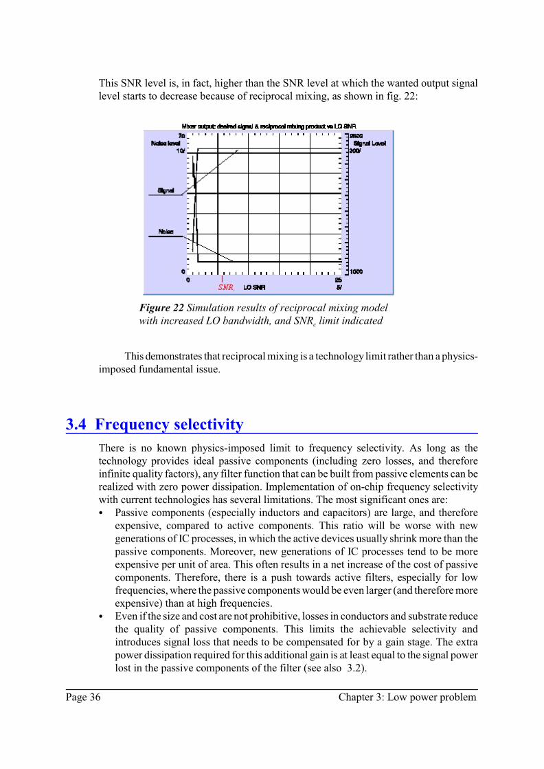
Page 36 Chapter 3: Low power problem
This SNR level is, in fact, higher than the SNR level at which the wanted output signallevel starts to decrease because of reciprocal mixing, as shown in fig. 22:
This demonstrates that reciprocal mixing is a technology limit rather than a physics-imposed fundamental issue.
3.4 Frequency selectivity
There is no known physics-imposed limit to frequency selectivity. As long as thetechnology provides ideal passive components (including zero losses, and thereforeinfinite quality factors), any filter function that can be built from passive elements can berealized with zero power dissipation. Implementation of on-chip frequency selectivitywith current technologies has several limitations. The most significant ones are:C Passive components (especially inductors and capacitors) are large, and therefore
expensive, compared to active components. This ratio will be worse with newgenerations of IC processes, in which the active devices usually shrink more than thepassive components. Moreover, new generations of IC processes tend to be moreexpensive per unit of area. This often results in a net increase of the cost of passivecomponents. Therefore, there is a push towards active filters, especially for lowfrequencies, where the passive components would be even larger (and therefore moreexpensive) than at high frequencies.
C Even if the size and cost are not prohibitive, losses in conductors and substrate reducethe quality of passive components. This limits the achievable selectivity andintroduces signal loss that needs to be compensated for by a gain stage. The extrapower dissipation required for this additional gain is at least equal to the signal powerlost in the passive components of the filter (see also 3.2).
Figure 22 Simulation results of reciprocal mixing model
cwith increased LO bandwidth, and SNR limit indicated

Chapter 3: Low power problem Page 37
(19)
C The limited accuracy of on-chip components requires special techniques for circuitswith high selectivity, especially when the relative bandwidth is close to, or evensmaller than, the relative frequency spread caused by the frequency-determiningcomponents. In these cases, tunable components and calibration circuits are oftenneeded.
C To overcome the limitations of passive devices, active filters are used whensignificant selectivity at lower frequencies is required. These filters inherentlydissipate power in the gain, transconductance, and/or gyrator elements that are usedin such filters. For transconductor filters, the power dissipation P of a singletransconductor-capacitor (gm-C) element depends on the required signal-to-noise
0 0ratio SNR, the required quality factor Q , the resonance frequency f , the noise factorF and the efficiency 0 [35]:
Selectivity is especially an issue for long-range systems, since, in these systems,spectrum efficiency is an important concern, and interference is a significant problem inthe system design. The selectivity requirements for short-range systems are often morerelaxed, with one important exception: several short-range systems, such as Bluetoothand IEEE 802.11b WLAN, operate at frequencies in Industrial, Scientific and Medical(ISM) bands. These bands are intended as “garbage areas” in which industrial, scientificand medical equipment can (within limits) radiate electromagnetic power that isgenerated as part of their intended operation. For example, consumer microwave ovensuse RF energy in the 2.4GHz to 2.5GHz ISM band to heat food. A very small fraction ofthis power leaks out of the shielded cavity in which the food is heated. Since the powerof such a microwave oven is very high (in the order of 700W to 1000W) to allow it toheat food very quickly, even that very small fraction is still several orders of magnitudehigher than, for example, the 1mW of transmit power allowed for a class III Bluetoothdevice. Therefore, selectivity for short-range systems in the ISM band has a significantimpact on the performance of these devices.
3.5 Other operations
In addition to the elementary operations, i.e. gain, frequency shift, and frequencyselectivity, many other operations are required to complete the RF transceiver:C electro-magnetic field to electrical signal conversion at the antennaC analog-to-digital conversion at the ADCC digital-to-analog convertsion at the DACC RF switchingC Received signal strength indication (RSSI) extractionC channel switchingC power management

Page 38 Chapter 3: Low power problem
C isolation of the electronics from impedance changes of the antennaC directional coupling
These operations have not been discussed, either because they are not part of the RFsignal chain (e.g. RSSI extraction, channel switching, power management, analog-to-digital and digital-to-analog conversion), or because they are not usually implementedinside the IC (EMF to signal conversion, RF switching, isolation, directional coupling).The functions implemented by these operations have a limited interaction with theelementary operations defined before. The main interactions are shown in table 5.
Gain Frequency conversion Selectivity
Antenna T T
ADC T T
DAC T T
RF switches T
RSSI
channel switching
power management
isolator T
directional coupler T
Table 5 Interaction between functions and elementary operations
As table 5 shows, there is no interaction between any of these operations andfrequency conversion. The interaction with gain is, in many cases, just a compensationfor losses in operations like the antenna, switches, isolator, and directional coupler. Theantenna provides a significant contribution to the band selectivity in some systems. Sincethe functions of these elements cannot be implemented using the three elementaryoperations, and since the interactions between these operations and the elementaryoperations are rather weak, the elementary operations can, for the most part, beinvestigated independently of these functions.
There is, however, a strong interaction between the elementary operations gain andselectivity and the operations ADC and DAC. The performance of the ADC, as well asthat of the DAC, determine the point at which the signal processing can be convertedfrom the analog to the digital domain and vice versa. Due to improvements in dataconverter performance, the point at which this transition occurs is shifting more and moretowards the antenna. Currently, the systems which are the focus of this research areusually implemented with digital demodulation and analog frequency conversion. Thedata converters are therefore located somewhere in the channel selectivity part of thetransceiver. Moving them closer to the mixers, with less frequency selectivity in between,increases the performance requirements of the data convertors. There are two reasons forthis:C In the receive chain, the reduced frequency selectivity results in stronger interferers
at the ADC input, requiring both higher sampling rates and a larger dynamic rangeof the ADC.
C In the transmit chain, the reduced selectivity results in stronger spurious signals fromthe quantized and time-discrete DAC output, requiring both higher sampling rates andlarger dynamic range of the DAC.

Chapter 3: Low power problem Page 39
With the power dissipation of a data converter at least proportional to both thesample rate and the number of quantization levels, in many systems it is not yet feasibleto move the data converters all the way to the mixers without any channel selectivity inbetween, since this would result in prohibitive power dissipation of the data converters.On the other hand, the performance of current data converters is often sufficient to allowlow power implementations without full channel selectivity between the mixers and thedata converters.
This could in principle be a gradual process, in which the data converters shifttowards the mixers pole by pole over time. System partitioning considerations oftenprevent this scenario. Many companies have developed implementations that arepartitioned between a digital CMOS part and an analog CMOS, BiCMOS or even GaAsRF part. If the partitioning is such that one part of the channel selectivity is implementedin one IC, and the other part in the other IC, then the only way to build a transceiver withthe correct performance is by using these two IC’s in combination. At first, this mightseem an advantage for the companies, since it will encourage customers to buy theircomplete radio as a chip set. However, it also requires both IC’s to be competitive, orcustomers might prefer to mix and match RF and digital IC’s from different companies.Such customers will require interfaces that are compatible with other vendors’ IC’s,thereby limiting the freedom in partitioning the transceivers between the analog anddigital domain. As a consequence, some attention to the impact of the elementaryoperations on the data converters is justified, but since not all partitionings are practical,this discussion will be rather limited.
3.5.1 Other systemsThus far, it was implicitly assumed that all three elemental operations are essential forall systems relevant to this research. Recently, however, there has been a lot of interestin systems that are rather different from most other systems. Especially some time-domain ultra-wideband systems (UWB), which use pulses to transmit their information,rather than a modulated carrier, could result in very different transceiver topologies andfunctions. For example, frequency conversion might not be required, or even feasible, forchannels that span from 3GHz to 10GHz. Such systems will require different approachesat both the system level and circuit design level.
On the other hand, some of the newer proposals in the UWB standardizationcommittees are moving in the direction of multiple sub bands and even more traditionalmodulated-carrier approaches, such as OFDM and wideband spread spectrum. For suchsystems, the approaches in this thesis do apply.
3.6 Summary and conclusions
In this chapter, three elementary operations in an RF front end have been identified:gain, frequency conversion, and selectivity. For each of these operations, the fundamentaland physics imposed limits have been identified. Table 6 shows the fundamental limits,imposed by physics and technology, that have been identified for each of the threeelementary operations.

Page 40 Chapter 3: Low power problem
Gain Frequency
Conversion
Selectivity
Physics
limitsLOPAE#100% P $
LO2 k T f ln(2)
P = 0
Technology
limits
Table 6 Overview of fundamental and technology limits for elementary operations
The technology limit equations at the top for gain and frequency conversion arevalid for short-range systems, and the equations at the bottom for long-range systems.The technology limits expression for selectivity at the top is valid for active filters, themiddle one for passive filters in short-range systems, and the bottom one for passivefilters in long-range systems. The linearity and gain referred to in these last twoexpressions refer to the gain stages that compensate for the losses in the passive filters.
Reciprocal mixing is not limited by physics, but by technology, as has been shownin 3.3. Increasing the bandwidth in the LO input stages of the mixer will reducereciprocal mixing to arbitrarily low levels.
For practical circuits, the minimum power dissipation set by laws of physics isexceeded by quite a large margin, often multiple orders of magnitude, and determinedmostly by technology limitations. This is very encouraging, since further reductions ofpower dissipation are likely with improvements in technology. A reduction in powerdissipation might also be achieved with current technologies, by using improved systemand circuit designs and design methods.

Chapter 4: A case study: the DECT front end Page 41
Chapter
4A case study: the DECT front end
This chapter discusses the design of a low-power, zero-IF, DECT RF front endimplemented in BiCMOS. This design was carried out around 1993, using a conventionalcustom design approach, which is still the most popular design approach. This makes ita very suitable benchmark for the other designs and design methods introduced later inthis thesis. It also provides the systems background needed in later chapters.
4.1 Introduction
The current European cordless phone system is called the Digital European CordlessTelecommunications (DECT) system, which extends the cordless phone concept in thedirection of large pico cellular systems for both speech and data communication. DECTis a short-range system, and therefore the emphasis for this design was on low powerdissipation at high frequencies.
Section 4.2 introduces the DECT system and design targets, and Section 4.3explains the principles of zero-IF receivers with their advantages and limitations. Thedesign of the receiver is discussed in Section 4.4. Implementation and results are shownin Section 4.5.

Page 42 Chapter 4: A case study: the DECT front end
4.2 The DECT system
In this section we will introduce some aspects of the DECT physical layer [90] that affectthe design of DECT receivers. DECT implements wireless ISDN-compatible speech anddata links using a network of overlapping base stations not unlike a cellular system suchas GSM. However, the range of the base stations, and hence the distance between them.is much smaller than in traditional cellular systems. A typical DECT system can have cellsizes in the order of several hundred meters outdoors, and tens of meters indoors. Thisallows for very high traffic densities in a traditional cordless environment such as thehome and office. Such small cells make DECT unsuitable for traditional cellular systemswith nationwide coverage. Applications for DECT range from fully wireless PBX(private branch exchange) systems in large office complexes, spanning several sites withfully transparent operation, to the traditional use as a single cordless phone around thehouse. Local area networks (LAN) or connections from the public phone network toextensions in existing neighborhoods are other areas in which DECT offers an efficientand flexible alternative to other systems.
To optimize the use of the available spectrum, the DECT standard divides both thefrequency band and the time into chunks that can be flexibly allocated to a number ofsimultaneous connections.
4.2.1 Frequency allocation DECT systems use a frequency band in the 1.88GHz to 1.90GHz range. This range isdivided into 10 channels with a channel spacing of 1.7MHz per channel. Modulation isGaussian Minimum Shift Keying (GMSK) with a bandwidth-time product (BT) of 0.5[91]. This provides a compromise that is less bandwidth efficient, but easier to implementthan the modulation chosen for e.g. GSM. Transmission power is 0.25W, which issignificantly higher than other cordless systems (typically 10mW), but much lower thantraditional cellular systems (typically several Watts).
4.2.2 Time slot structure Each channel is divided into frames. Each frame consists of 24 time slots (fig. 23). Oneframe takes 10ms, and a slot about 0.4ms. A standard full-duplex connection consists oftwo slots per frame. One slot is used for communication from handset to base station,while the other slot is used for communication in the opposite direction. Therefore, thetransmitter and receiver in a handset are alternately activated with a duty cycle of 1/24 ,th
resulting in a time-division-duplex (tdd) operation. Each slot contains 420 bits, which are used for synchronization (32 bits), control (64 bits)and data (324 bits). The raw bit rate of a channel is 1.152Mbit/s, and the net bit rate ofa standard full-duplex connection is 32kbit/s. Slots can be split into two half slots, andsubsequent slots can be linked to provide flexible assignment of communication capacity.
The channel and slot which a connection uses are dynamically allocated to provideoptimum reception and least interference. This also allows overlapping of base stationswithout complicated static channel assignments in advance. Transparent hand-overbetween base stations is also provided for.

Chapter 4: A case study: the DECT front end Page 43
Figure 23 Timeslot structure of a DECT signal
Figure 24 System diagram of a DECT transceiver
4.2.3 DECT transceiver architecture In fig. 24 a block diagram of a typical DECT transceiver is shown. It consists of atransmitter and a receiver, connected to a common antenna through a switch. The receiverand transmitter are provided with the required oscillator signals from a synthesizer block,which can be implemented with either one or two synthesizers. The output of the receiverand the input of the transmitter are connected to the burst mode controller, a digital ICresponsible for the real-time parts of the protocol such as bit, slot and framesynchronization. The higher protocol levels and the user interface are implemented insoftware on a micro controller, which controls synthesizer, burst mode controller, antennaswitch, and transmit and receive modes. The micro controller is also connected to akeyboard and display.
The codec is an ADPCM speech encoder/decoder which interfaces the compresseddigital representation of speech to and from the analog signals which go to theloudspeaker and come from the microphone. In this section we will concentrate on thereceiver aspects of DECT. As is obvious from fig. 24, this is only a small part of the totaltransceiver system.
4.2.4 Requirements The DECT standard defines a relatively complicated communication protocol comparedto other cordless systems. This will require rather complex digital circuits (codec, burstmode controller, micro controller). Some advantages of this protocol (high traffic density,

Page 44 Chapter 4: A case study: the DECT front end
ISDN compatibility, wide application area) have already been discussed in the previoussections. The features of the DECT standard also affect the design of the receiver frontend. Some of them make the design simpler, others more complicated. These features andtheir impact are listed below.
Features that make the design simpler:C The relatively large transmission power, small cell size, and low SNR required for
good quality digital transmission allow for relatively relaxed receiver sensitivity. C Distortion requirements are also moderate. Even though a DECT system in an office
environment might be interference limited, the dynamic slot selection avoids manyproblems.
C The low duty cycle of the transmitter allows a high transmission power of 250mWwith an average power dissipation of only 10mW, which is comparable to othercordless systems. The receiver also benefits from this low duty cycle, although, unlikethe transmitter, it also has to be activated occasionally to check for incoming calls,even when the phone is not in a call.
C The antenna duplex filter typically found in cordless and cellular systems is notrequired in DECT, since the transmitter and receiver are never active simultaneously.In fact, a duplex filter is not even possible, since transmission and receptionfrequency are typically the same. Some kind of antenna switch might still be required.
Features that make the design more complicated:C The RF frequency is higher than in most other cordless systems (typically 900MHz
or lower). This requires more emphasis on RF design, and components and ICprocesses with improved RF behavior.
C The digital circuits are relatively complex compared to other cordless phones. Sincethe power dissipation of these circuits is expected to decrease with improvements intechnology, their contribution to overall power dissipation will eventually becomenegligible. For now, the additional dissipation of these circuits has to be compensatedfor by lower power dissipation of the receiver. The relative importance of the receiverdissipation obviously depends on the ratio between active and stand-by operation ofthe transceiver.
C Since the digital circuits are relatively complex and add significantly to thecomponent count, a minimum number of components and adjustments is as importantin DECT as it is in other portable systems.
C To take advantage of the low duty cycle, the receiver must be capable of beingpowered up and switched off very quickly, within a fraction of a millisecond.
The next section will investigate the suitability of conventional and zero-IFreceivers for DECT applications.

Chapter 4: A case study: the DECT front end Page 45
Figure 25 Conventional receiver architecture and signals
4.3 Zero-IF receivers
Conventional receivers mix the antenna signal (RF) with a local oscillator signal (LO)to obtain an intermediate frequency (IF), which can then be filtered for channel selectivityand be demodulated (fig. 25). In such a receiver, a trade-off exists for the frequency ofthe IF signal. High IF frequencies require difficult-to-implement channel-selectivityfilters and demodulators, while low IF frequencies require difficult-to-implement image-rejection filters in front of the mixer. Often, this trade-off does not yield the requiredresults, and a double-conversion receiver has to be used. Such receivers require morefilters, mixers and oscillators, resulting in increased space, weight, power dissipation, andcost.
4.3.1 Zero-IF receiver architecture These problems can be avoided by choosing the IF frequency at, or very close to, zero.The IF frequency is in this case much lower than the bandwidth of the signal. Receiverswhich apply this architecture are called zero-IF receivers.
To distinguish between positive and negative IF frequencies which correspond tothe upper and lower sideband of the RF signal, a second mixer and filter branch is usedin the receiver. In this second branch, an LO signal of the same frequency but differentphase is used to drive the mixer. The two IF signals are commonly labeled I and Q (fig.26).

Page 46 Chapter 4: A case study: the DECT front end
Figure 26 Zero-IF receiver block diagram
The phase difference between the LO signals is ideally 90 degrees. The sign of the phasedifference between I and Q can be used to distinguish between positive and negativefrequencies.
4.3.2 Advantages Zero-IF receivers have several obvious advantages: C The channel selectivity filter can be fully integrated since it can be implemented as
a low-pass filter. Such a filter does not require high-quality or very accuratecomponents, since the components only determine the bandwidth of the filter. The“center” frequency (0Hz!) is correct by construction.
C Interference problems related to IF signals do not occur, since the signal frequenciesare very low.
C Only a single LO signal is required, and in the case of DECT, this signal has the samefrequency as the transmitter. Usually, it can be derived from the same source as thetransmitter signal. In a conventional receiver, this could also be achieved, but it ismuch more difficult because of the short frequency switching time required of the LOsource when switching between send and receive.
C An image rejection filter is unnecessary, although some antenna selectivity might berequired in a practical implementation.
C Since it is possible to integrate the receiver completely, it is in principle possible toachieve much better control over crosstalk than with a conventional receiver whichrequires external components. Moreover, it allows higher impedance levels to be usedat high frequencies, reducing the power dissipation.
C The low frequencies in the IF part of the receiver can decrease the power dissipationas well.
4.3.3 Disadvantages The disadvantages and limitations of a zero-IF receiver are not always apparent at first.They include: C The dual receiver branches of a zero-IF receiver might consume more power than the
single branch of a conventional receiver. C The accurate 90 degrees phase-shift circuit and well-matched filters can only be
implemented easily on an IC. For example, even a wire length difference of just 200micrometers will introduce a phase error of about 1 degree at 2GHz. Therefore,

Chapter 4: A case study: the DECT front end Page 47
integration is not just possible, it is virtually mandatory. C A fully integrated receiver implemented in a typical silicon IC process cannot apply
high-quality inductors or strip lines. This will result in reduced performance and/orincreased power dissipation.
C Crosstalk from the LO signal to the RF signal causes loss of sensitivity andinterference. Loss of sensitivity occurs because the receiver converts the crosstalk toa DC level at IF. This DC level is in the middle of the IF band. Removing it byfiltering will remove part of the received signal as well, and thus reduce sensitivity.Changes in frequency and environment will change the amount of crosstalk and theresulting DC level. Permanent adjustment is therefore not possible, and the lowestcut-off frequency of the filter is limited by the rate at which the crosstalk changes. Ina DECT receiver, the quick changes in frequency and environment (body effect) willmake this a difficult problem. The choice of an appropriate filter type, optimized forthis application, can provide an acceptable solution to this problem. LO to RFcrosstalk will cause interference, since the antenna filter and the antenna are bydefinition designed to effectively interface electrical signals of the LO frequency intoradio waves. These radio waves can then interfere with other DECT receivers.
C A zero-IF receiver requires a special demodulator which can derive the modulationsignal from two IF signals around zero. Since the baud rate of the IF signal is highcompared to its center frequency, zero crossings of the IF signal do not occurfrequently enough to derive the modulation signal from them. This also implies thatlimiting the IF signals is not possible without losing information (appendix E).
4.3.4 Comparison A zero-IF architecture is an attractive choice for a DECT receiver because of the smallsize, low weight, few adjustments, simple antenna filter, single simple synthesizer, andrelaxed DECT requirements for sensitivity and distortion. Power dissipation could endup comparable to a conventional receiver design because of the combined advantages anddisadvantages of zero IF in this respect. This does require that the disadvantagesmentioned in the previous section can be overcome by careful design, as will bediscussed in the next section.
4.4 Design
The main specifications for this DECT receiver are shown in table 7. The noise figure of9dB is in line with the low emphasis on sensitivity expected from a short-range system,as is the relaxed linearity specification of -28dBm for the third-order intercept point (IP3).The main challenges are the combination of a high RF frequency of 1.9GHz and the lowpower dissipation of 90mW. These specifications have been divided into specificationsfor the RF front end and the IF part of the receiver. This allowed for the concurrentdesign of these two parts as two separate ICs. Ultimately, these two designs could becombined into a combined RF/IF IC. The specifications for the RF front end are shownin table 8.
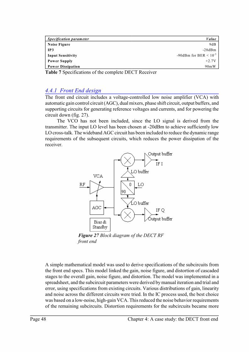
Page 48 Chapter 4: A case study: the DECT front end
Specification parameter Value
Noise Figure 9dB
IP3 -28dBm
Input Sensitivity -90dBm for BER < 10-3
Power Supply +2.7V
Power Dissipation 90mW
Table 7 Specifications of the complete DECT Receiver
4.4.1 Front End design The front end circuit includes a voltage-controlled low noise amplifier (VCA) withautomatic gain control circuit (AGC), dual mixers, phase shift circuit, output buffers, andsupporting circuits for generating reference voltages and currents, and for powering thecircuit down (fig. 27).
The VCO has not been included, since the LO signal is derived from thetransmitter. The input LO level has been chosen at -20dBm to achieve sufficiently lowLO cross-talk. The wideband AGC circuit has been included to reduce the dynamic rangerequirements of the subsequent circuits, which reduces the power dissipation of thereceiver.
A simple mathematical model was used to derive specifications of the subcircuits fromthe front end specs. This model linked the gain, noise figure, and distortion of cascadedstages to the overall gain, noise figure, and distortion. The model was implemented in aspreadsheet, and the subcircuit parameters were derived by manual iteration and trial anderror, using specifications from existing circuits. Various distributions of gain, linearityand noise across the different circuits were tried. In the IC process used, the best choicewas based on a low-noise, high-gain VCA. This reduced the noise behavior requirementsof the remaining subcircuits. Distortion requirements for the subcircuits became more
Figure 27 Block diagram of the DECT RFfront end

Chapter 4: A case study: the DECT front end Page 49
severe because of the high gain, but since DECT requirements for third-order distortionare rather moderate, this was not a problem.
Second-order distortion was reduced by implementing the subcircuits with balancedsignals. This also reduced noise injection and sensitivity to ground, supply and substratenoise. By means of several iterations, the specifications of the subcircuits as shown intable 9 were arrived at.
Specification parameter Value
Voltage gain: 8dB to 37dB
Noise figure: 6dB
IP3: -25dBm
IP2: +14dBm
LO input level: -20dBm
LO to RF leakage: -60dBm
Input impedance: 50S
Phase matching: 4°
Amplitude matching: 1dB
Power Supply Voltage: +2.7V
Power Dissipation: 45mW
Table 8 Specifications of the RF front end circuit
Power dissipation for the mixer, VCA, and phase shift circuits was initially set at25% of the total power budget each. The remaining 25% could then be spent on outputbuffers and support circuits.
4.4.2 Package At 1.9GHz, the package parasitics are so significant that they have to be taken intoaccount as an integral part of the design. The package selected for this design is a plasticSO16, a small outline 16-pin package. A bondwire of such a package at 1.9GHz alreadyhas an impedance of about 70jS, which cannot easily be neglected for 50S inputs.Inclusion of the package in impedance matching is therefore mandatory.
The package also plays a significant role in the LO-to-RF crosstalk. Simulationshave shown that even an empty package with unbalanced LO and RF signal pins achievesonly 20dB of isolation, because it resonates around 2GHz. Since the RF input has to besingle-ended to facilitate application of the front end, there was no choice but to make theLO input balanced. In this way, an empty package achieves about 45dB of isolation.
4.4.3 Voltage-controlled low-noise amplifier The VCA input transistor is a common emitter, biased at 1.5mA, with an inputimpedance of 50-20jS (fig. 28). The capacitive part of this input impedance is more thancompensated for by the bondwire of the package. The pin next to the RF input is used forRF ground. Internally, it is connected to the emitter of the input transistor. By connectingthe pin through an AC-coupling capacitor to the ground of the antenna filter, the RFcurrents will run through these neighboring pins and bonding wires instead of runningthrough the power and ground wires across the IC. Adding a decoupling capacitor of theappropriate value to the RF input will tune out the remaining inductive part of the inputimpedance. The resulting overall input impedance is now 50S.
This semi-balanced pin arrangement also provides additional isolation to LO

Page 50 Chapter 4: A case study: the DECT front end
crosstalk. The gain of the input transistor is controlled by adjusting the collector currentby means of an AC-decoupled MOS transistor. The gate of this transistor is controlledby the output of the AGC circuit. The output of this first stage has a source impedanceof 500S and is still unbalanced. An output stage converts the signal to a balanced signalat a lower impedance. By choosing the resistor values R_c2 and R_e2 the same, andidentical to R_c1, the load currents will only flow through the output transistor, and theAC collector current of the input transistor will compensate for the AC collector currentof the output transistor. This provides reduced noise injection into the supply rails andthe substrate, and also reduces sensitivity of the VCA to noise on the supply and in thesubstrate. Like the first transistor, the output transistor also runs at 1.5mA, and providesan output impedance of approximately 50S differential. The outputs of the VCA areconnected to the RF inputs of the mixers. A more detailed diagram of the circuit is shownin fig. 29.
LNA Mixer Output Buffer
Voltage gain: 20dB 13dB 4dB
Power gain: 20dB -4dB 8dB
Noise figure: 3.5dB 10dB 18dB
IP3: -20dBm 220mV 1V
Power dissipation:
(design target)
10mW 10mW 10mW
Power dissipation:
(realized)
13.5mW 10.5mW 6mW
Table 9 Specifications of the Subcircuits
Between the input transistor and the output stage, an emitter follower has beenintroduced to reduce the capacitive load of the output stage. The peak detector of theAGC loop is implemented with a differential pair (TNS_1,TNS_2) that compares thecollector signal of the input transistor to a DC-shifted and low-pass filtered version ofitself. The output of the threshold detector is fed through a series of amplifiers and a timeconstant (external to this circuit) to the gate of the NMOS transistor which sets the gainof the input transistor.
Figure 28 Schematic diagram of a voltage-controlled low-noise amplifier

Chapter 4: A case study: the DECT front end Page 51
Figure 29 Detailed diagram of VCA

Page 52 Chapter 4: A case study: the DECT front end
Figure 30 Mixer schematic diagram
4.4.4 Mixers The mixers are implemented as common 6-transistor double-balanced circuits (fig. 30).This provides good isolation from LO to RF inputs, and eliminates straight feedthroughof the RF signal. The noise behavior of the switching stage of such a mixer is rathercomplex. The noise contribution of the switching stage can be reduced by increasingswitching transistor size until the noise contribution is negligible compared to the inputstage. Since the output frequencies are so low, the collector-substrate capacitance of suchdevices is not likely to be a problem. In a design optimized for low power, however, thismight not be the best solution. The input impedance of the switching transistors woulddecrease when the transistor sizes increase, requiring LO buffers with a lower outputimpedance. Since the LO buffers need a gain of about 20dB, this would result in asignificant increase in power dissipation. Instead, an optimum size was found for noisebehavior by fixing the power dissipation of the LO buffers and changing the size of theswitching transistors.
The optimum switching transistor size was relatively small, and insufficient for theDC current of the input stage. Therefore, most of this current is routed through resistorsdirectly to the power supply. Additional benefits from the smaller currents includesmaller diffusion capacitors of the switching transistors, and higher voltage gain of themixer because of increased output resistor values.
4.4.5 Phase shift circuit The phase shift circuit needs to generate two LO signals with a phase accuracy of about2 degrees. This leaves 2 degrees for mismatches in the mixers and output buffers.Common solutions include frequency dividers and allpass filters [9]. Frequency divisionwould require a frequency doubler on chip, since the 3.8GHz signal is not available fromthe synthesizer. Generating and dividing such a high frequency would have increasedpower dissipation significantly. Allpass filters do not need this double frequency, but therequired components could not be implemented with sufficient accuracy and quality with

Chapter 4: A case study: the DECT front end Page 53
Figure 31 Principle of phase shift circuit
(27)
the available technology.Therefore, a passive RC phase shift circuit was applied that is based on the inherent
90° phase difference between the current through, and the voltage across, a capacitor. Byfeeding the capacitor current through a resistor, the voltage across the resistor andcapacitor will differ by 90° independent of frequency, or resistor and capacitor values.Naturally, the amplitudes of the voltages will change with frequency. The use of limiterscan eliminate this problem for a very wide frequency range (fig. 31).
The main error source in this circuit is the capacitive loading of the limiter inputson the central node of the RC network. The IC technology used for the implementationof this circuit provides poly-silicon resistors with small parasitic capacitances and metalplate capacitors with small series resistance. These parasitics of the RC network arenegligible compared to the load of the limiters. The capacitor does have a parasiticcapacitance to the substrate, but only from the bottom plate. By implementing thecapacitor as a triple-plate structure with the middle plate connected to the central nodeof the RC network, the parasitic capacitance of this plate to the substrate also becomesnegligible compared to the load of the limiters.
The source impedance of the LO signal does not affect the phase error directly. However,a low source impedance allows a low-impedance RC network to be used, which is lesssensitive to capacitive loading. This circuit achieves power dissipation levels much lowerthan similar circuits that have been reported before [92].
A diagram with the implementation details of the phase shift circuit is shown in fig.33. The RC network is followed by emitter followers to reduce the parasitic load on thecentral node of the RC network. The error introduced by capacitive loading of the centralnode is shown in fig. 32. The load of the emitter followers is mainly capacitive andamounts to approximately 20fF. In order to achieve equal delays through the emitterfollowers, a dummy limiter input circuit has been added across the outer two emitterfollowers.
Another source of phase errors is introduced by the distortion of the LO signalitself. This error can be analyzed by determining the zero-crossing positions of the output
insignals of the RC network when a distorted signal is applied to it. Define V as the LO
1 2 2source voltage with a required frequency component f and a distortion component f (f
1= n f ):

Page 54 Chapter 4: A case study: the DECT front end
Figure 32 Phase error introduced by loading
(28)
I QNow the voltages across the resistor and capacitor can be defined as V and V ,
inwhich can be expressed in the components of the LO signal V according to the followingformulas:
I QThe relative positions of the zero crossings of V and V define the phase differencebetween the signals. Solving for this phase difference yields a function F(a,j), whichrelates the phase difference F to the distortion level a and the relative phase j of the
1 2 1 2 1frequency components f and f = n f . Fig. 34 shows a plot of this function for f = 3 f .

Chapter 4: A case study: the DECT front end Page 55
Figure 33 Detailed diagram of the phase shift circuit

Page 56 Chapter 4: A case study: the DECT front end
Figure 34 Phase error introduced by third order LO distortion
Figure 35 Simulation results of the phase shift circuit
Phase accuracy has been simulated for the actual circuit at less than one degreeacross a frequency range from 100MHz to 3GHz (fig. 35).

Chapter 4: A case study: the DECT front end Page 57
Figure 36 IF circuit block diagram
4.4.6 IF circuit A full discussion of the IF circuit (fig. 36) is beyond the scope of this thesis. Thesuppression of the DC component due to LO crosstalk can be optimized by anappropriate filter type at the inputs of the IF circuit. This is followed by lowpass channelselectivity filters and AGC circuits. A demodulator derives the modulation signal bycombining the I and Q signals and their derivatives. The output of the demodulator ispassed through a data slicer to obtain well-defined logical levels.
4.5 Implementation and results
The front-end circuit has been implemented in a 1: BiCMOS process. The mainparameters of the minimum bipolar device are shown in table 10. The layout of the circuithas been optimized for symmetry and matching, and minimization of crosstalk, as can beseen in fig. 38.
RF measurements on the wafer are not possible because of the large number of RFand DC signals that have to be applied simultaneously. Also, since the package was anintegral part of the design, the performance of the circuit without package would not meetthe requirements. Building a set-up which allowed quick replacement of test devices andalso provided sufficiently accurate RF behavior proved to be rather involved. LOcrosstalk in particular is difficult to measure, since crosstalk across a test board can easilyexceed the crosstalk of the device. This was solved by building a measurement set-up asshown in fig. 37. The base of this set-up was made of metal, and had two slopes with thesame angle as the pins of an SO16 package. On these slopes, two printed circuit boards(PCB) were mounted, with traces that lined up with the pins of the SO16 package at thetop. These traces were designed as 50S micro-strip lines, and connected the signals toSMA connectors at the other end of the PCB (not shown). A mechanical clamp (notshown) was used to push the packaged front end securely down on top of the PCBs,ensuring a good contact between package pins and PCB traces. Power supply linedecoupling was implemented through CMC capacitors very close to the pins of the IC.This set-up allowed measurements of RF performance at 2GHz with an isolation betterthan 70dB between the LO and RF traces on the PCBs.

Page 58 Chapter 4: A case study: the DECT front end
Figure 38 Die photo of the DECT front end
Crosstalk measurement results are shown in fig. 39. These measurement results areclose to the package model simulation.
Figure 37 Measurement set-up

Chapter 4: A case study: the DECT front end Page 59
Figure 39 LO crosstalk measured at the RFinput
Figure 40 I and Q output signals of the frontend
This is consistent with the observation that powering down the front end actuallyincreases the crosstalk. The phase accuracy of the phase shift circuit cannot be measuredseparately for the same reasons that make it impossible to implement the phase shiftcircuit externally. Therefore, only the phase shift accuracy of the complete front end hasbeen measured, and it is within specifications. In fact, it is within the accuracy limits ofthe phase meter used for these measurements. Fig. 40 shows the I and Q signals on anoscilloscope, which gives results close to the phase meter readings.
Distortion of the circuit is shown in fig. 41 below, and corresponds to an IP3 of !23dBm.
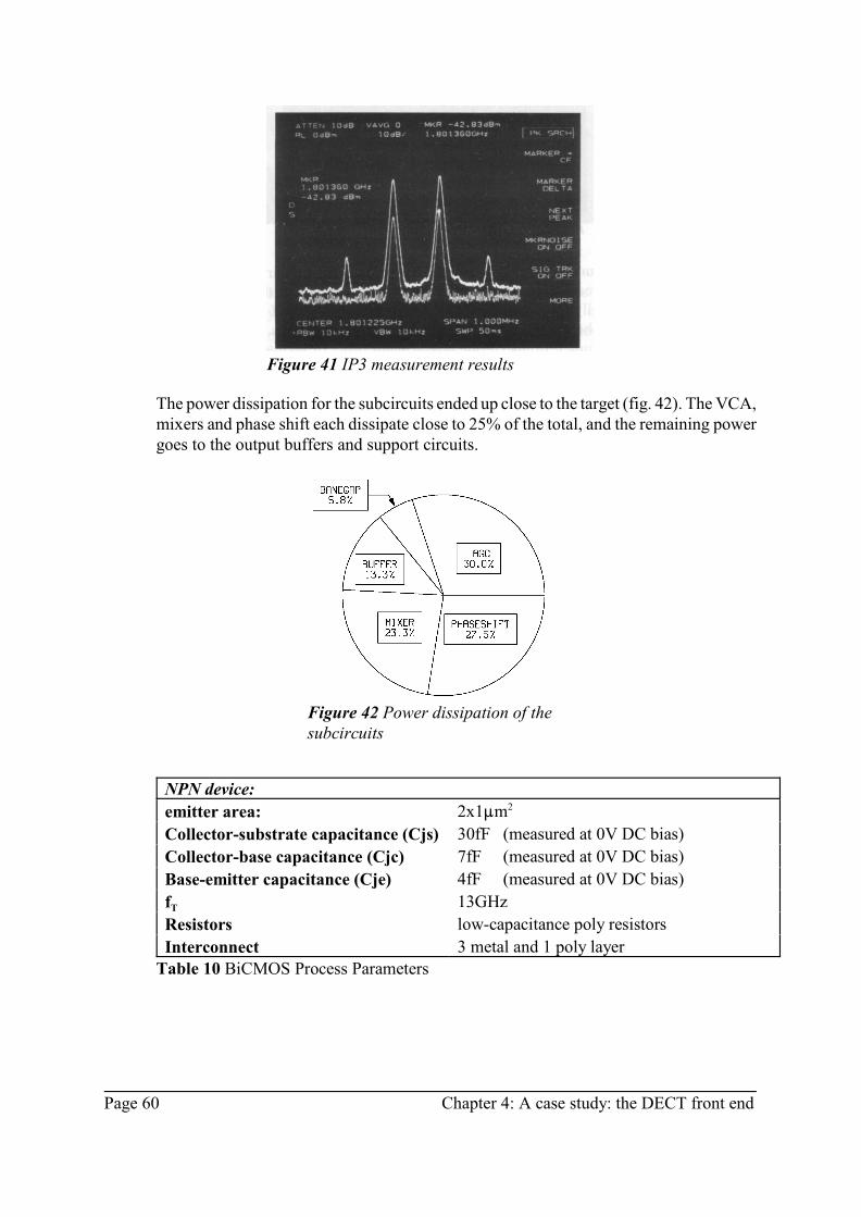
Page 60 Chapter 4: A case study: the DECT front end
Figure 41 IP3 measurement results
Figure 42 Power dissipation of thesubcircuits
The power dissipation for the subcircuits ended up close to the target (fig. 42). The VCA,mixers and phase shift each dissipate close to 25% of the total, and the remaining powergoes to the output buffers and support circuits.
NPN device:
emitter area: 2x1:m 2
Collector-substrate capacitance (Cjs) 30fF (measured at 0V DC bias)
Collector-base capacitance (Cjc) 7fF (measured at 0V DC bias)
Base-emitter capacitance (Cje) 4fF (measured at 0V DC bias)
Tf 13GHz
Resistors low-capacitance poly resistors
Interconnect 3 metal and 1 poly layer
Table 10 BiCMOS Process Parameters

Chapter 4: A case study: the DECT front end Page 61
(29)
4.6 Summary and conclusions
Zero-IF receivers offer several advantages for DECT receivers, such as low weight, smallsize, few external components and adjustments, simple antenna filter, and single simplesynthesizer. In order for a zero-IF receiver to be a real alternative to conventionalreceivers, several disadvantages such as phase accuracy and LO leakage need to beovercome. The receiver front end described in this section demonstrates that it is possibleto solve these issues by careful design, using standard design methods. This resulted ina fully integrated receiver front end with a performance and power dissipationcomparable to a conventional receiver.
In order to compare the power dissipation of this design to the fundamental limitsidentified in Section 3.6, we compare the LNA and output buffers to the “Gain”elementary operation, and the Mixer to a combination of the “Gain” and “FrequencyConversion” elementary operations (table 11).
Gain Frequency Conversion Total Physics
limit
LNA at min signal 0.000001% NA 13.5mW 100pW
LNA at max signal 1% NA 13.5mW 0.1mW
Mixer at min signal -0.00000061% 10:W 10.5mW -50pW
Mixer at max signal -0.6% 10:W 10.5mW -60:W
Buffer at min signal 0.0000021% NA 6mW 212pW
Buffer at max signal 2.11% NA 6mW 251:W
Table 11 Power dissipation of LNA, mixer and output buffer compared to fundamentallimits
The results in table 11 are shown for two conditions: the signal levels at minimumantenna signal, i.e. the sensitivity limit of the receiver, and the signal levels at maximumantenna signal. The reason for including both conditions is that the circuits are using classA type biasing for the active devices. This makes the efficiency very much dependent onthe signal levels, as is obvious from the numbers in the table.
The minimum output level of the LNA is -70dBm, derived from the -90dBmsensitivity limit and 20dB of gain. The power dissipation is 13.5mW, resulting in a PAEof:
The maximum output level of the LNA is approximately -10dBm, the 1dBcompression point. This results in a PAE of:

Page 62 Chapter 4: A case study: the DECT front end
(30)
(31)
(32)
(33)
For the mixer, the input signal levels are 20dB higher, and the output signal level is 4dBlower, corresponding to the power gain of the mixer. This results in a PAE at minimumsignal levels of:
The PAE is negative because the output power is lower than the input power, while thecircuit still dissipates additional power from the power supply. The power gain of lessthan 1 is due to the 2.5kS differential output impedance of the mixers. The fundamentallimit for the power level of a 1.9GHz LO signal is 10.7pW, based on formula 12 inSection 3.3. This brings the fundamental limit for the power dissipation of the mixer to10.7pW-61pW=-50.4pW. The actual power level for the LO signal is 10:W, about sixorders of magnitude higher.
The maximum input level of the mixer is about -10dBm, and therefore themaximum output level is !14dBm. This results in a PAE of:
The minimum input level of the output buffer is -74dBm. With 8dB of gain, theminimum output level is -66dBm or 251pW. This results in a PAE of:
It is clear that at low signal levels, the main cause for the power dissipation is theclass-A biasing of the circuits. At high signal levels, the power dissipation is still one totwo orders of magnitude above the fundamental limits. This power dissipation is mainlycaused by the high signal frequencies for the LNA and mixer, which require a minimumbiasing of the active devices to achieve sufficient gain.
The power dissipation in the output buffer is mainly determined by therequirements for driving IF signals up to 5MHz off-chip. In the original design

Chapter 4: A case study: the DECT front end Page 63
specifications, an off-chip parasitic capacitance of 15pF was taken into account. Theoutput current, and therefore the biasing, of the buffer is set by the highest slope of theoutput signal, in combination with this parasitic capacitance, even though no outputpower is delivered to this capacitor.

Page 64 Chapter 4: A case study: the DECT front end

Chapter 5: A minimum-power design method Page 65
Chapter
5A minimum-power design method
A new design method is required to design front ends that achieve the requiredperformance with the minimum power dissipation possible, within a set of boundaryconditions. Such a design method will be called a minimum power design method in thecontext of this thesis. In this chapter, such a new design method will be developed.
The method is based on circuit transforms that can be applied to any circuit. Suchtransforms are called “structure-independent transforms”, or SITs, and consist of amathematical transformation of the specifications of a circuit, and a correspondingtransformation of the circuit that achieves such a transformation of specifications. Basedon a collection of such SITs, two orthogonal SITs (or OSITs) are derived that are usedas the basis for a minimum power design method. In this design method, the signal pathof a front end is considered as a cascade of signal processing circuits, such as LNAs,mixers, filters, etc. Using the OSITs, the specifications, including the power dissipation,of the individual circuit blocks can be changed, resulting in different overallspecifications and overall power dissipation. Any given overall specification of the frontend, if possible at all, can be achieved by an infinite number of combinations oftransformed signal processing circuits. There is only one combination of transformedsignal processing circuits that results in the minimum overall power dissipation, and acorresponding unique distribution of gain, linearity and noise specifications across thesubcircuits. This optimum distribution of power dissipation, gain, linearity and noise hasbeen found and can be represented as a number of analytical expressions. Based on theoutcome of these expressions, the optimum transforms can be selected for the individualsubcircuits.
A practical minimum design method also needs selection criteria for a library ofinitial signal processing circuits that will be used in an RF front-end design. A selectioncriterium for these circuits is a special figure of merit (or FOM), that transforms thespecifications of a circuit into a one-dimensional performance criterium. The circuits with

Page 66 Chapter 5: A minimum-power design method
the best figure of merit can then be used as the basis for a front end with an optimumdistribution of gain, linearity, noise, and power dissipation, as described above. A specialclass of figures of merit, called equivalent figure of merit, or EFOM, will be introducedin Section 5.4. This EFOM is based on OSITs, which allow the specifications of anycircuit with a specific EFOM value to be transformed to exactly the specifications ofanother circuit with the same EFOM value.
As a demonstration of the potential of this approach, the power dissipation of aDECT front end with transformed circuits is calculated, based on the specifications andcircuits of the DECT front end from the previous chapter.
5.1 Design flow
The goal of RF front-end design is the development of a physical implementation that,in combination with other designated system components, can meet the specifications fora target system.
Figure 43 Front end design process
A typical front end design process consists of five consecutive stages, as shown in fig.43.
Derivation of front-end specsThe transceiver specs are derived from the system specs (fig. 44). They can be found bytaking into account the antenna specifications and the IF&baseband specifications. If thechoice of the antenna and/or IF&baseband circuit is not yet fixed, all possiblecombinations can be investigated. The results of this investigation can be used to supporta decision for a specific antenna and/or IF&baseband circuit. If the front end has to workwith multiple antenna and/or IF&baseband circuits, the same method can be applied, butnow the worst-case combination of all specification parameters can be used for the frontend specification. Either way, the resulting specification is unique, and no iterations(other than for multiple antenna and IF&baseband circuits) are required within the firststage. Still, the first stage does suffer from two shortcomings that affect designproductivity:

Chapter 5: A minimum-power design method Page 67
Figure 44 Stage 1 in the front enddesign process
First, if people in charge of the design process change their mind about the projecttargets, e.g. because of new market inputs, or because of changes in interfacespecifications, the design process typically needs to be restarted from stage 1. If theprocess has already advanced to a later stage, this results in a significant delay in theproject, and reduction in productivity.
Second, the information required to derive front end specifications is not alwaysreadily available in a format that is easy to access. Also, knowledge of, and experiencewith, the procedure for deriving front end specs from system specifications might beinsufficient.The first shortcoming depends on many external factors. It can be reduced by formal riskassessments such as “failure mode and effect” analysis, by better project managementmethods, and by padding specifications to allow for some changes during the project. Thesecond shortcoming could be minimized by storing the knowledge of relevant systemsin such a way that it is easy to access for the incidental user, and by providingdescriptions or even automation of the spec derivation procedure. Systems knowledge isavailable through e.g. ETSI CD-ROMs, books, internet sites etc. The information fromthese sources is seldom in a consistent format, however. In practice, it takes a lot ofexperience or an even larger amount of patience to understand the system requirementsbased on these sources. Partial derivation procedures are available through many home-brewn spreadsheets and simple software tools. These are seldom integrated into thedesign process, and documentation is often minimal, requiring again experience orpatience from the designer who wants to use such tools.

Page 68 Chapter 5: A minimum-power design method
Figure 45 Stage 2 of the front end design process
Derivation of subcircuit specsThis is essentially an optimization problem with some fixed boundary conditions(typically specs such as sensitivity and power supply voltage) and optimization criteria(typically cost, power dissipation, etc.), as shown in fig. 45. It is therefore the same typeof derivation as the first step, but at a lower abstraction level. Often, this also includes adifference in span of control. In many front end developments the standards at the systemlevel cannot be changed. The front end product specification is often open for somedebate.
If, for each of the subcircuits, the trade-offs between specs for the fixed boundaryconditions and the optimization criteria are known, then the problem can be solvedthrough mathematical analysis. However, the trade-offs for the subcircuits depend oncircuit topologies and parameter values, of which an infinite number of combinationsexist. Therefore, a formal optimization is impossible. Attempts have been made togenerate all possible circuit topologies [73] and to automatically find optimum parametervalues [65], but they cannot cope with the typical complexity of front-end subcircuits inrealistic periods of time, so another approach is required.
Design, fabrication and verificationThese are steps that, at an abstract level, are straightforward once stage 2 has been
completed, since in this stage the desired specifications of the sub blocks are known.However, in practice, the performance of a subcircuit depends significantly on itsenvironment because of effects like substrate noise, packaging parasitics, crosstalk, etc.This is the main reason why a full top-down approach to RF front end design is notfeasible. It is not possible to cope with the level of complexity inherent in all significanteffects at the higher levels in a top-down process, and therefore abstraction does notwork. Until this problem is solved, there is no alternative for experience and detailedinsight.For this same reason, it does not make sense to spend a lot of effort on detailedand highly accurate simulations and optimizations at a high abstraction level of an RFfront end design.
An optimal design procedure is both efficient (i.e. requires the minimum amountof resources) and effective (i.e. the result is as close as possible to a predefined goal. Aminimum power optimal design procedure should achieve both goals, and the resulting

Chapter 5: A minimum-power design method Page 69
Figure 46 Typical design procedure with iterationloops
front end should achieve the lowest possible power dissipation within a given set ofboundary conditions. Typical design procedures do not meet the requirement forefficiency, because of the many iterations that are part of such a design method. Figure46 shows the design procedure of fig. 43 with the most common iteration loops. Thecircuit design block has been split into the sub blocks “circuit design” and “simulation”,in the shaded area in the center of the figure, to emphasize the inner loop of the designprocess. For an optimum design procedure, it is necessary to eliminate these iterations asmuch as possible. The iterations consume time, and therefore reduce the efficiency of thedesign procedure. Also, it is not possible to find the best front-end and circuit topologyfrom an infinite number of topologies with a finite number of iterations. Therefore, inpractice, the effectiveness of this procedure is also less than optimum.
5.2 A SIT and EFOM based design procedure
It would be useful if the first steps in a top-down design method could be carried outmore efficiently. This would result in a selection of front end topologies, subcircuitspecifications and subcircuit topologies that, within the limits of the abstraction, definethe global optimum solution for power dissipation. Because of the limits of theabstractions used, this global optimum will not be highly accurate, but it will be the beststarting point for a front end implementation. This implies that some iterations in theimplementation stages might still be required, but with the fundamental limits providedin this thesis, the margins are now well understood.
This can be achieved by defining a library with a finite number of circuit and front-
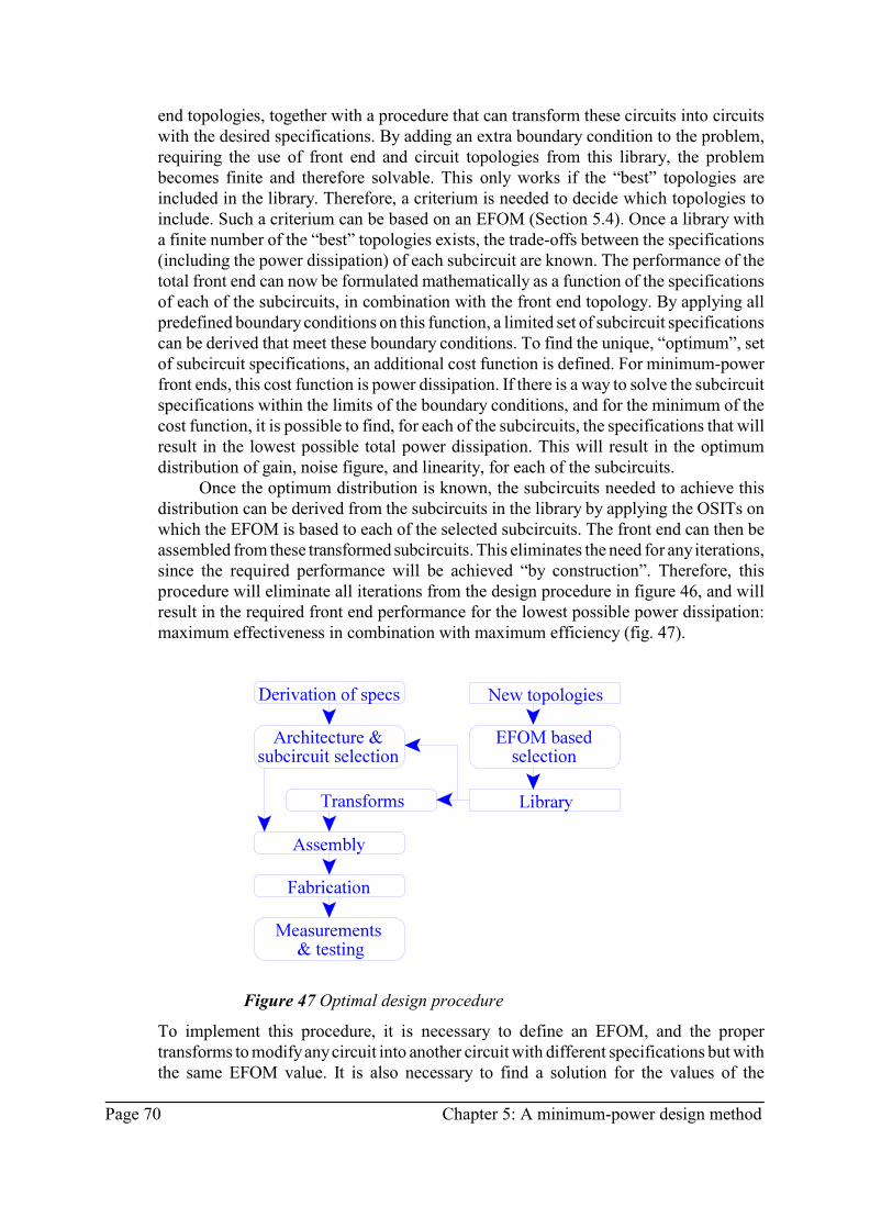
Page 70 Chapter 5: A minimum-power design method
Figure 47 Optimal design procedure
end topologies, together with a procedure that can transform these circuits into circuitswith the desired specifications. By adding an extra boundary condition to the problem,requiring the use of front end and circuit topologies from this library, the problembecomes finite and therefore solvable. This only works if the “best” topologies areincluded in the library. Therefore, a criterium is needed to decide which topologies toinclude. Such a criterium can be based on an EFOM (Section 5.4). Once a library witha finite number of the “best” topologies exists, the trade-offs between the specifications(including the power dissipation) of each subcircuit are known. The performance of thetotal front end can now be formulated mathematically as a function of the specificationsof each of the subcircuits, in combination with the front end topology. By applying allpredefined boundary conditions on this function, a limited set of subcircuit specificationscan be derived that meet these boundary conditions. To find the unique, “optimum”, setof subcircuit specifications, an additional cost function is defined. For minimum-powerfront ends, this cost function is power dissipation. If there is a way to solve the subcircuitspecifications within the limits of the boundary conditions, and for the minimum of thecost function, it is possible to find, for each of the subcircuits, the specifications that willresult in the lowest possible total power dissipation. This will result in the optimumdistribution of gain, noise figure, and linearity, for each of the subcircuits.
Once the optimum distribution is known, the subcircuits needed to achieve thisdistribution can be derived from the subcircuits in the library by applying the OSITs onwhich the EFOM is based to each of the selected subcircuits. The front end can then beassembled from these transformed subcircuits. This eliminates the need for any iterations,since the required performance will be achieved “by construction”. Therefore, thisprocedure will eliminate all iterations from the design procedure in figure 46, and willresult in the required front end performance for the lowest possible power dissipation:maximum effectiveness in combination with maximum efficiency (fig. 47).
To implement this procedure, it is necessary to define an EFOM, and the propertransforms to modify any circuit into another circuit with different specifications but withthe same EFOM value. It is also necessary to find a solution for the values of the

Chapter 5: A minimum-power design method Page 71
subcircuit specifications that achieve the minimum of the cost function while meeting allboundary conditions. Finally, it is necessary to formulate the steps of the designprocedure in such a way that they can be carried out within a very short period of time,e.g. by automating the individual steps.
Naturally, such a design procedure is limited by the accuracy of the models onwhich the EFOM is based, and by the parameters taken into account in the performancedefinition and transforms. All parasitic effects that are not included in these models, andall parameters lacking from the performance definition and transforms, will affect theresult of the design procedure. As a result, additional work is required to arrive at anoptimum front end. Nevertheless, by including the most relevant parameters in theperformance definition, and the most critical effects in the models, a good firstapproximation of optimum subcircuit specifications will be obtained, as well as a clearmethod with which these specifications can be achieved through transforms of circuittopologies from the library. Therefore, this design procedure will result in a first designthat is close to the global optimum. Such a design can be turned into a fully optimizedcircuit with relatively little effort. The design procedure will also provide a quickindication of the power dissipation that is ultimately achievable for a given set ofperformance requirements and boundary conditions.
5.3 Structure independent transforms (SITs)
The number of circuit topologies is so large, that it is impractical to take all possibletopologies into account. For the same reason, it is not practical to consider circuittransformations that are specific for a circuit topology. Practical transforms shouldtherefore be independent of the circuit topology or structure, in other words, they shouldbe Structure Independent Transforms, or SITs. In order to find such transforms, themodel from Section 3.1 will be used. In this model, the signal processing in the RF frontend is implemented using a cascade of two-port signal-processing stages, that carry outone or more of the elementary operations of the RF front end. Some blocks, such asmixers, have in reality more than two ports. They can nevertheless be modeled as a twoport, as long as the signals on the other ports are well-defined (e.g. the local oscillatorsignal in a mixer). This approach will be used throughout this section.
To assess the impact of transforms on the performance of a signal-processing stage,some assumptions about the main performance parameters are required. The mainparameters in RF front ends are gain, noise and distortion, as discussed in appendix A.Since the focus of this thesis is on minimum power design, the power dissipation is, ofcourse, an additional relevant parameter. To assess the impact of cascading the circuits,the input and output impedances are relevant as well. Therefore, the design space thatwill be considered for minimum power design methods has the following dimensions:
dc ingain (G) noise factor (F), linearity (IP3), power dissipation (P ), input impedance (Z )
outand output impedance (Z ). Since most telecommunication systems are relativelynarrow-band, all these parameters are defined at a single signal frequency.

Page 72 Chapter 5: A minimum-power design method
Figure 48 Impedance transform
(34)
5.3.1 A set of structure independent transformsIn this section, signal-processing stages are modeled as imperfect building blocks with
p ina power gain G , noise factor F, third-order intercept point IP3, input impedance Z ,
out dcoutput impedance Z and power dissipation P . Using this model, a collection of SITswill be discussed. All of them are known transforms. What is new is the formaldescription as a transform, and the matching mathematical description of thetransformation of the specifications. This allows the transforms to be used in a genericway, and therefore become the basis of a general design method. This collection of SITsis by no means exhaustive. Fortunately, completeness is not required for a minimumpower design method. The SITs will be used to derive the orthogonal transforms neededto adjust each of the relevant performance parameters. As will be shown in the nextsection, this collection provides a more than sufficient basis for the required orthogonaltransforms.
To simplify the expressions, it is assumed that all source and output impedancesare, initially, equal. This is not essential for the transforms. If required, differentimpedance levels can be modeled by putting an additional impedance transformer at theinput or the output of a building block.
Impedance transformIn narrow-band systems, a low loss transformer with an impedance transformation ratio" can often be implemented cheaply at the PCB level, and sometimes (depending on theIC technology) also on chip. When put in front of our building block, an impedancetransform with a factor " changes the input impedance, but leaves all other performance
parameters unchanged. However, this transform is a very useful part of other SITs. Thecorresponding transform of the specifications is shown in (34).

Chapter 5: A minimum-power design method Page 73
Figure 49 Paralleltransform
(35)
Parallel transformThe parallel transform puts two identical circuit blocks in parallel. These blocks areshown as amplifier symbols in fig. 49. As a result of this transform, the input and outputimpedances are reduced by a factor of 2, the gain and noise figure remain unchanged, andthe IP3 and power dissipation are increased by a factor of 2. The input and outputimpedances can be restored by applying impedance transforms with "=2 at the input and"=0.5 at the output. At the circuit level, this transform is equivalent to doubling the W/Lratio of lateral devices and the active area of vertical devices, not taking into accountimperfect scaling. As a result, the node voltages in the circuit will remain the same,whereas the branch currents will double, and the impedance levels will go down by afactor of 2. This transform can in principle be carried out by any factor, not just 2. Pleasenote that the transform with a factor smaller than 1 is not always possible for technologieswith vertical devices, since halving the W/L ratio of lateral devices is in principlepossible, but halving the area of vertical devices is limited by lithography and possiblyother boundary conditions in IC fabrication. Obviously, a process that allows accurate
scaling down to very small currents offers more flexibility with respect to this transform.The corresponding transform of the specifications is shown in (35).

Page 74 Chapter 5: A minimum-power design method
Figure 50 Cascade transform
(36)
Cascade transformWhen cascading blocks, the gain increases exponentially as a function of powerdissipation, which seems very attractive. However, both the noise figure and the IP3deteriorate compared to a single block. If the gain is high compared to the noise factor,then the total noise figure will be only slightly higher than the noise figure of a buildingblock. However, in this case the intercept point will decrease approximatelyproportionally to the increase of the gain. The corresponding transform of thespecifications is shown in (36).
Parallel-cascade hybrid transformBy combining the cascade and parallel transforms, it is possible to approximate atransform that increases the gain while keeping noise figure and IP3 constant. This is
pachieved by putting G +1 groups of two cascaded building blocks in parallel. For gainsmuch larger than 1, the power dissipation increases proportionally to 2 times the gain

Chapter 5: A minimum-power design method Page 75
Figure 51 Parallel/cascade hybrid transform
(37)
increase. For building blocks with lower gain, this effect is even worse. Obviously, gainis expensive. If the gain is much larger than the noise factor, the noise factor does notchange significantly. It would perhaps be more obvious to build this hybrid transform bycascading a first stage, consisting of two parallel building blocks, and a second stage,
pconsisting of 2 G building blocks in parallel. The stages would then be coupled throughan impedance transform with " = Gp. This is more consistent with the common practicein receivers, in which the IP3 of subsequent stages is increased about proportionally tothe gain accumulated up to that point. This results in the same gain vs. power dissipationtrade-off, and therefore the same SIT. The corresponding transform of the specificationsis shown in (37).

Page 76 Chapter 5: A minimum-power design method
Figure 52 Attenuation transform
(38)
Attenuation transformAttenuation is typically easy to implement both on and off chip. It is assumed that theattenuator itself does not introduce additional noise. The dynamic range of the totalcircuit is not significantly affected, but the gain is reduced, and the noise figure isincreased by the same factor as the attenuation. Note that the inverse transform, addinggain in front of the original circuit, is in principle also a valid SIT. However, it is moredifficult to implement, and the performance is much more technology dependent.Therefore, it is not as convenient a SIT as the attenuation transform. The correspondingtransform of the specification parameters is shown in (38).
Mismatch transformMismatch is different from attenuation, in the sense that the excess input power is notdissipated but reflected. This is true both for signal and noise power. Since the excessinput power is not dissipated, no excess noise is generated and the noise figure is notaffected. The corresponding transform of the specification parameters is shown in (39).Mismatch is also different from the other transforms in this section in the sense that itchanges the matching between circuits. All other transforms are based on the assumptionthat the match between source, load, and circuit block will not be changed. In most on-chip RF circuits, there will be significant mismatches between circuit blocks, bothbecause matching circuits are expensive to build on-chip, and because this increases therobustness of the IC performance with respect to process and environmental changes. Themismatch transform is the only transform that changes this (mis)match. It is attractive

Chapter 5: A minimum-power design method Page 77
Figure 53 Mismatch
(39)
because it offers a trade-off between gain and linearity without affecting the noisebehavior of a circuit.
Distortion cancellation transformA very interesting class of transforms is the class of distortion cancellation transforms.These transforms are based on the principle that the ratio between distortion componentand signal component is generally dependent on the signal level. By processing (at leasttwo) different levels of the same signal through identical circuits, it is possible to obtaintwo distorted signals with different signal-to-distortion ratios. By adding these twodistorted signals with appropriate gain factors, it is possible to cancel a distortioncomponent while preserving (part of) the signal.
In principle, a perfect cancellation can be obtained for a single distortioncomponent. In practice, the reduction is limited by the matching that can be achievedbetween the branches. By recursively applying this procedure, all distortion componentscould be eliminated. Obviously, this is impractical for more than two or threecomponents because of the cost and power dissipation of the circuits involved. Fig. 54shows a distortion cancellation diagram with two branches.

Page 78 Chapter 5: A minimum-power design method
Figure 54 Distortion cancellation
A widely used distortion cancellation transform is balancing, which can be used to cancelsecond order components. In this case, alpha=1 and beta=-1. Also, third ordercancellation is sometimes used, e.g. in “multi-tanh” circuits. In the case of two branches,the coefficients should be chosen such that beta=-1/alpha^3 (in order to cancel the thirdorder component) and beta�-1/alpha (otherwise the wanted signal would be suppressed).
Distortion cancellation transforms are special in that they trade accuracy forlinearity. Accuracy is required both in terms of matching between the elements in the twobranches and absolute accuracy of the coefficients alpha and beta. There is no real trade-off between distortion cancellation and power dissipation. In general, there can be animpact on the gain and noise figure. For the second-order distortion cancellation there isno such penalty, since there is no reduction of the signal level or signal-to-noise ratio. Forthe third-order distortion cancellation, there is a finite penalty in terms of the gain andnoise figure, but this can be made arbitrarily (and infinitesimally) small by choosing largevalues of alpha. A large value of alpha will cause the third order distortion componentto become relatively large compared to the wanted signal as well as to the noise. Only asmall fraction of the output, corresponding to a small beta, is required to cancel thedistortion component, and this small version of beta will result in small effects on thenoise and wanted signal levels.
Therefore, there is no significant trade-off between distortion cancellation and gain,noise figure or power dissipation for second- and third-order distortion cancellation. Thisimplies that distortion cancellation always yields improvement independent of othertransforms applied to the circuit, and is only limited by practical considerations. Thetransform of the specification parameters for the second order distortion cancellationtransform is shown in (40), and for the “infinitesimal penalty” case of the third orderdistortion cancellation transform in (41).

Chapter 5: A minimum-power design method Page 79
(40)
(41)
Feedback transformFeedback is again a special transform, in the sense that it is not obvious to implement forprocessing stages that include the frequency conversion elementary operation. This wouldrequire an additional frequency conversion elementary operation in the feedback path,and this additional frequency conversion will itself have the same impairments, such asdistortion and noise generation, that feedback is supposed to reduce. Therefore, feedbackcannot be considered a structure independent transform in the strict sense.
Even for signal-processing stages that do not include the frequency conversionoperation, implementing feedback while maintaining the power match is not trivial, andmerits a separate investigation.
5.3.2 Orthogonal SITs (OSITs)The transforms described in the previous section are somewhat arbitrarily selected fromthe infinite number of possible transforms. Most of the transforms also affect multipleparameters simultaneously, but not independently. For an efficient minimum powerdesign method, a minimum set of optimum, orthogonal transforms is required.C Optimum transforms are defined here as transforms that achieve any desired
performance with the lowest power dissipation for any performance of the originalcircuit.
C Orthogonal transforms are defined here as transforms that have each at least onespecification parameter that is invariant through the transform, and this parameter isdifferent for all orthogonal transforms. The transforms are called orthogonal becausethe vectors in design space corresponding to the invariant parameter of any

Page 80 Chapter 5: A minimum-power design method
orthogonal transform is orthogonal to all other invariant vectors of other orthogonaltransforms.
Orthogonal structure-independent transforms (OSITs) for power, gain and linearity canbe found by combining the parallel transform and the mismatch transform. This resultsin two orthogonal transforms:1. The OSIT_1 transform, consisting of a parallel transform with a parameter “mult”
indicating the (fractional) number of stages that should be connected in parallel,preceded and followed by impedance transforms with parameters “1/mult” and“mult”, respectively. This transform only affects power dissipation and IP3,without affecting gain and noise figure. It is shown in figure 55.
Figure 55 OSIT_1 transform
2. The OSIT_2 transform, a combination of the OSIT_1 transform and mismatch
11 11with parameter “s ”, as shown in fig. 56, under the condition s =mult. Thisaffects gain and power dissipation without affecting noise figure and IP3. The
transformation of transformer K3 corresponds to , and is therefore
11responsible for the mismatch with factor s .
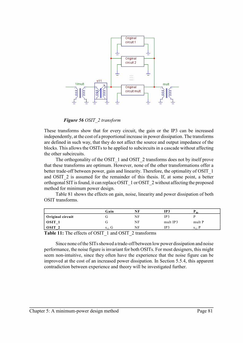
Chapter 5: A minimum-power design method Page 81
Figure 56 OSIT_2 transform
These transforms show that for every circuit, the gain or the IP3 can be increasedindependently, at the cost of a proportional increase in power dissipation. The transformsare defined in such way, that they do not affect the source and output impedance of theblocks. This allows the OSITs to he applied to subcircuits in a cascade without affectingthe other subcircuits.
The orthogonality of the OSIT_1 and OSIT_2 transforms does not by itself provethat these transforms are optimum. However, none of the other transformations offer abetter trade-off between power, gain and linearity. Therefore, the optimality of OSIT_1and OSIT_2 is assumed for the remainder of this thesis. If, at some point, a betterorthogonal SIT is found, it can replace OSIT_1 or OSIT_2 without affecting the proposedmethod for minimum power design.
Table 81 shows the effects on gain, noise, linearity and power dissipation of bothOSIT transforms.
dcGain NF IP3 P
Original circuit G NF IP3 P
OSIT_1 G NF mult IP3 mult P
OSIT_2 11 11s G NF IP3 s P
Table 11: The effects of OSIT_1 and OSIT_2 transforms
Since none of the SITs showed a trade-off between low power dissipation and noiseperformance, the noise figure is invariant for both OSITs. For most designers, this mightseem non-intuitive, since they often have the experience that the noise figure can beimproved at the cost of an increased power dissipation. In Section 5.5.4, this apparentcontradiction between experience and theory will be investigated further.

Page 82 Chapter 5: A minimum-power design method
(43)
(44)
5.4 Equivalent figures of merit (EFOMs)
1OSITs transform any circuit, with a performance represented by a point P in the m-dimensional space V, into another circuit with a different performance, represented by a
2 ipoint P . The set of points P that can be covered by applying all possible OSITs on acircuit, when taken together, form a hyperplane A in V. Any circuit with a performancerepresented by a point on A can therefore be considered to have a performance equivalentto any other circuit with a performance represented by any other point on A.
This equivalence is the foundation for a new class of figures of merit (FOMs),called “equivalent figures of merit”, or EFOMs. EFOMs are a subset of FOMs, since theyrequire the existence of transforms that can be applied to any circuit. These transformsshould generate all new circuits with combinations of performance parameters that havethe same EFOM value. This requirement allows EFOMs to be used directly in a designprocess: the circuit with the best EFOM value is always the best basis for any other setof specifications, as long as the performance parameters in the EFOM and in thespecification are identical. The base circuit can then be transformed into the requiredcircuit using OSITs. This sets EFOMs apart from other FOMs: they are much more than“just another FOM”.
The OSIT_1 and OSIT_2 transforms from the previous section are an ideal basisfor developing an EFOM. OSIT_1 allows for a proportional trade-off between power andlinearity. OSIT_2 allows for a proportional trade-off between gain and linearity. Sincethey are orthogonal, they can be combined easily. The combination allows a proportionaltrade-off between power and the product of gain and linearity. This combined trade-offcan be represented by an EFOM, which in this thesis will be called the power linearityfactor 6:
dcIt relates the power dissipation P of a circuit to its gain G and linearity IP3. Sincethe output IP3 (OIP3) equals the product of gain and input IP3, this is equivalent to:
This is the reason for naming k the power linearity factor. k is invariant under theOSITs defined in previous section. Note that 6 increases with increasing powerdissipation, and decreases with increasing gain and linearity. In other words, circuits witha low 6 are more desirable for low power design.
Since circuits with a dominant pole also allow a trade-off between gain andbandwidth (Section 3.2), and since there is often no significant dependence of IP3 andpower dissipation on the signal frequency, the power linearity factor for this class of
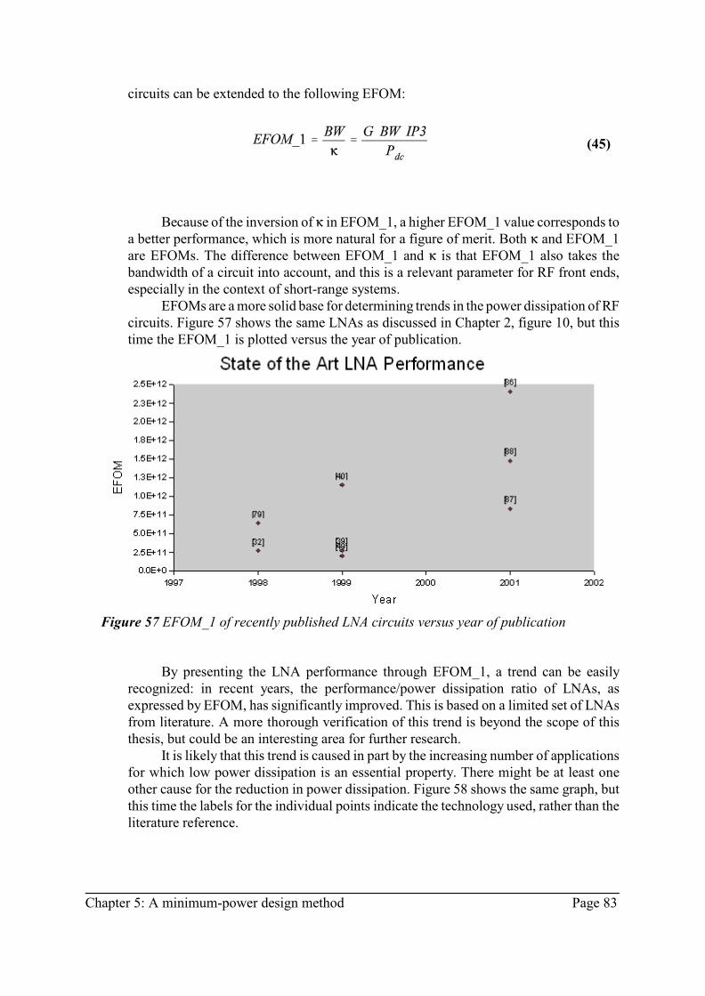
Chapter 5: A minimum-power design method Page 83
(45)
Figure 57 EFOM_1 of recently published LNA circuits versus year of publication
circuits can be extended to the following EFOM:
Because of the inversion of 6 in EFOM_1, a higher EFOM_1 value corresponds toa better performance, which is more natural for a figure of merit. Both 6 and EFOM_1are EFOMs. The difference between EFOM_1 and 6 is that EFOM_1 also takes thebandwidth of a circuit into account, and this is a relevant parameter for RF front ends,especially in the context of short-range systems.
EFOMs are a more solid base for determining trends in the power dissipation of RFcircuits. Figure 57 shows the same LNAs as discussed in Chapter 2, figure 10, but thistime the EFOM_1 is plotted versus the year of publication.
By presenting the LNA performance through EFOM_1, a trend can be easilyrecognized: in recent years, the performance/power dissipation ratio of LNAs, asexpressed by EFOM, has significantly improved. This is based on a limited set of LNAsfrom literature. A more thorough verification of this trend is beyond the scope of thisthesis, but could be an interesting area for further research.
It is likely that this trend is caused in part by the increasing number of applicationsfor which low power dissipation is an essential property. There might be at least oneother cause for the reduction in power dissipation. Figure 58 shows the same graph, butthis time the labels for the individual points indicate the technology used, rather than theliterature reference.
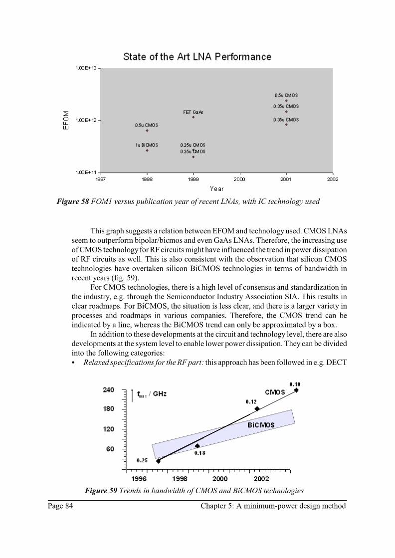
Page 84 Chapter 5: A minimum-power design method
Figure 58 FOM1 versus publication year of recent LNAs, with IC technology used
This graph suggests a relation between EFOM and technology used. CMOS LNAsseem to outperform bipolar/bicmos and even GaAs LNAs. Therefore, the increasing useof CMOS technology for RF circuits might have influenced the trend in power dissipationof RF circuits as well. This is also consistent with the observation that silicon CMOStechnologies have overtaken silicon BiCMOS technologies in terms of bandwidth inrecent years (fig. 59).
For CMOS technologies, there is a high level of consensus and standardization inthe industry, e.g. through the Semiconductor Industry Association SIA. This results inclear roadmaps. For BiCMOS, the situation is less clear, and there is a larger variety inprocesses and roadmaps in various companies. Therefore, the CMOS trend can beindicated by a line, whereas the BiCMOS trend can only be approximated by a box.
In addition to these developments at the circuit and technology level, there are alsodevelopments at the system level to enable lower power dissipation. They can be dividedinto the following categories:C Relaxed specifications for the RF part: this approach has been followed in e.g. DECT
Figure 59 Trends in bandwidth of CMOS and BiCMOS technologies

Chapter 5: A minimum-power design method Page 85
and BlueTooth standardization. The expectation was that the more relaxedspecifications of the RF circuits would result in lower power dissipation and lowercost. These results have been achieved only partially, at best, since IC vendors used“better than standard performance” as a differentiator in their competition, resultingin much higher than required RF performance and limited reduction in powerdissipation and cost.
C Low-power modes at system level: this approach takes power dissipation into accountalready in the early definition phases of a system. A typical example is the Japanesedigital video standard ISDB-T, in which a special mobile/low-power mode allows forthe reduction of the signal bandwidth (and therefore dynamic range, bitrates etc.)already at the antenna. Another example is the low-power standby mode inBlueTooth, which is achieved through low duty-cycle sampling of the radio signal tocheck for incoming data traffic.
C System-level low-power trade-offs: in this approach, the system trade-offs are basedat least in part on low-power considerations. For example, the total power dissipationof a receiver might be reduced by advanced antenna diversity systems, because suchsystems can significantly reduce the requirements for e.g. sensitivity, and thus morethan compensate for the power dissipation of the additional diversity circuits.
Obviously, these approaches can be combined as well, and such combinations areincreasingly used for systems targeted for low-power applications.
It is important to realize that equal performance, as indicated by the EFOM, doesnot imply equal desirability in every situation. Some combination of performance
aparameters, as represented by a point P , might be more desirable in a given application
bthan another set of performance parameters, as represented by a point P . For example,an amplifier with high gain and low linearity might be more desirable for someapplication than an amplifier that is derived from the original one through SITs, whichoffers a lower gain but higher linearity. In general, the “desirability” of parametercombinations can be identified through a cost function. Performance parametercombinations with equal desirability might be represented by another hyperplane B in V.The intersection of A and B represent the circuits that are equally desirable, and can bederived from a single circuit through SITs.
The desired performance of a circuit in a front end depends on the application ofthe front end, but also on the performance of other circuits in the signal chain. To find thedesired performance parameters of a circuit, it is necessary to find the optimumdistribution of performance parameters across a signal chain.
5.5 Optimum distribution of gain, linearity and noise
An optimum distribution of gain, noise and linearity for any front-end configuration andspecification can be derived, based on OSITs. In addition to the OSITs, expressions areneeded to relate the front end specifications to the circuit specifications of the signal-processing stages in the front end signal chain. These expressions will be discussed first.

Page 86 Chapter 5: A minimum-power design method
Figure 60 Cascaded stages
5.5.1 General ProblemThe general problem is shown in figure 60. Assume a cascade of signal-processing stagesnumbered 1 through n. Equations (46) show the relations between the overallspecifications and the performance of the individual blocks. The expression for the third-order distortion of cascaded stages is discussed in more detail in 8.7.1. The expressionfor total gain shows that the total gain is the product of the gain of the individual stages,and the expression for the total power represents the sum of the power dissipation of theindividual stages. The power of an individual stage is related to the gain and linearity ofthat stage through the power linearity parameter 6. The total noise factor, finally, isrepresented by Friis’ formula [4].
(46)
For the construction of an optimum distribution of gain, linearity, and noise in a frontend, it is assumed that a library of the “best” (as selected by EFOM_1) signal-processingsubcircuits is available from which such a front end will be constructed. For each of the

iEvery sub block can be characterized by its (transform invariant) nosie factor F and its power linearity4
i i i ifactor k . Each sub block then represents a class of potential sub blocks with different G , IP3 , and P , but with
ithe same k .
Chapter 5: A minimum-power design method Page 87
i ifront-end subcircuits in the library, the parameters F and k need to be known . If these4
parameters are not known, they can be easily derived by circuit simulation. The required
tot tot totperformance of the total front end is defined by F , G , and IP3 . Using OSITs, the
tot tot, totexpressions for cascaded noise factor F , linearity IP3 and gain G can be solved for
i i i totG and IP3 . If these parameters have been solved, P and P can be calculated as well.An infinite number of solutions exist. To find a unique solution, one more
totconstraint is needed: the solution has to achieve the global minimum value of P . Pleasenote that different constraints are possible, and sometimes even more relevant. Forexample, total chip area will in practice be a very relevant parameter for industrialdesigns. In order to determine the minimum power for a front end, however, this is themost relevant constraint in this case. Once the unique solution has been found, theminimum achievable power dissipation is known. In the next step, such a circuit can beassembled by applying the OSITs to the original subcircuits with the parametersdetermined by the solution. The resulting, new, subcircuits are then assembled into afront end circuit by cascading them according to the selected front end architecture.
There might be cases in which selecting the “best” subcircuits for the library is notobvious. For example, since the noise factor is a very relevant parameter for a front end,and since this parameter is not taken into account in the EFOM_1, the subcircuit with thebest EFOM_1 value might not have the best noise factor. In such a case, multiplesubcircuits of the same type can be added to the library, with different trade-offs betweennoise factor and EFOM_1. EFOM_1 can still be used to exclude circuits that don’t offereither a better EFOM_1 value or better noise factor, thereby significantly reducing thesize of the library. With multiple instances of the same type of subcircuit in the library,the minimum power dissipation needs to be calculated for every combination ofsubcircuits assembled according to the front end architecture. Once the minimum powerdissipation for every combination is known, selecting the best combination is trivial.
5.5.2 The solution for n=2For a cascade of two stages, the solution of these equations is straightforward. Theequations (46) for this case are:

Page 88 Chapter 5: A minimum-power design method
(47)
(48)
(49)
1 2 1 2 tot tot tot 1where k , k , F , F , F , G and IP3 are known. These equations can be solved for G ,
2 1 2G , IP3 and IP3 by first solving for the gains:
1Now IP3 can be calculated:
1 1 2Substituting G in (49) by the value from (48) results in explicit solutions for G , G and
1 2e.g. IP3 . What remains is the solution for IP3 . It would also have been possible to solve
2for IP3 first, which would of course result in the same solution. There are an infinite
2number of solutions for IP3 that satisfy the relations and known parameters. To find a
2unique solution for minimum power, P is expressed as a function of IP3 only, using the
1 2 1 1solutions for G , G and IP3 from the previous equations. A typical graph of IP3 as a
2function of IP3 is shown in fig. 61.

Chapter 5: A minimum-power design method Page 89
1 2Figure 61 IP3 as a function of IP3
(50)
(51)
2 1For IP3 values below, in this example, 4, no solution is found for P and IP3 . Whereas
1 2 2IP3 is a monotonic function of IP3 , P has a minimum for a specific value of IP3 . Thisminimum can be found by determining the extrema for P:
This expands to:
2 1 2 2This equation has two roots for IP3 : r and r (52). The root r has a positive second
1derivative and r has a negative second derivative.

Page 90 Chapter 5: A minimum-power design method
(52)
(53)
(54)
Since the positive second derivative in combination with a zero of the first derivative
2 2corresponds to a minimum, r represents the value of IP3 that corresponds to the
1minimum power dissipation. Please note that the power which corresponds to r actually
2represents a total power dissipation that can be lower than that represented by r .
1However, the corresponding value of IP3 is negative, and therefore represents no valid
2solution. Substituting r into the initial equations results in the following parametervalues:
The power level that corresponds to this solution is:
This is the minimum power dissipation that can be realized by any cascade of two stages.The corresponding solution for the gain and linearity (53) represents the minimum powerdistribution of gain, linearity and noise across two cascaded stages. It is of coursedesirable to extend this solution to more than two stages.

Chapter 5: A minimum-power design method Page 91
(55)
(56)
(57)
5.5.3 The General SolutionThe general problem for arbitrary values of n can be formulated as follows:
Given numbers:
find the minimum of:
i iand the corresponding values of G and IP3 , under the conditions:
This general optimization problem was solved mathematically by dr. ir. A.J.E.M. (Guido)Janssen, at the Philips Research Laboratories in Eindhoven, using Lagrange multipliers.The derivation of this solution can be found in appendix F. The solution for the gain,rewritten using the same parameters as in the problem definition above, is:

Page 92 Chapter 5: A minimum-power design method
(58)
(59)
(60)
(61)
(62)
The solution for IP3 can be rewritten as:
The minimum power dissipation can now be expressed as:
For n=2, this solution is of course identical to the solution found in the previous section.In the next step, a minimum power front end can be assembled by applying the
OSITs to the original subcircuits with the parameters determined by the solution (58)-(62).This will result in new subcircuits with the optimum gain and linearity for the frontend. These new subcircuits can then be assembled into a front end circuit by cascadingthem according to the selected front end architecture.

Chapter 5: A minimum-power design method Page 93
5.5.4 DiscussionThe general solution (62) has some interesting interpretations:C The total power dissipation scales with the total IP3 specification. This is to be
expected, since the OSIT_1 transform can also be applied at the front end level.C Even though there is no OSIT for noise factors at the subcircuit level, both the special
and the general solution show a trade-off between noise factor and power dissipation
i i iP=f(k , G , IP3 ) of the total front end. This is consistent with the experience of RFdesigners that low noise factors require high power dissipation at the front end level,and can be explained through Friis’ formula [4]. The total noise figure of multiple,cascaded, stages can be reduced by increasing the gain in the first stage. Increasingthis gain results in higher power dissipation. In addition, the linearity requirementsfor subsequent stages increases because of the larger signal levels, resulting in morepower dissipation of these stages as well. Therefore, this design method does providethe link between noise factor and power dissipation for the total front end, eventhough this is not obvious from the descriptions and transforms for the individualsubcircuits.
C The denominator of the second term in the main brackets equals the square root ofthe difference between the target noise factor and the noise factor of the first stage.When the noise figure of the first stage is higher than the total noise figure, nosolution is found, of course. This is consistent with the situation in which a too highnoise figure in the first stage cannot be compensated for by any means in subsequentstages.
C For first-stage noise factors lower than the total noise factor, the total powerdissipation increases rapidly when the noise factor of the first stage approaches thetotal noise factor. This makes sense, since a higher noise factor in the first stagewould require more gain in the first stage to reduce the noise contributions ofsubsequent stages. This will also result in higher signal levels in subsequent stages,and therefore higher linearity requirements, which in turn result in more powerdissipation.
C The numerator of the second term between the main brackets in (62) shows that theadditional power dissipation, caused by a higher noise factor in the first stage, isdependent on both the power linearity factors 6 of all stages but the last one, and theirnoise factors. The influence of the last stage is taken into account by the first termbetween the brackets.
5.6 A minimum-power front-end design procedure
A minimum-power design procedure, based on OSITs and EFOMs, will follow the stagesas have been shown in Section 5.2, fig. 47. The stages that are new and differentcompared to typical current design procedures have been shaded in figure 62. The designmethod uses standard stages for assembly, fabrication and measurement & testing. Also,new topologies are created using traditional methods. The hierarchy in abstraction levelsthat is introduced in this design method is required to build a model of reality in areduced form, which in turn is required both for developing an insight in the problem,and for a synthesis of the solution. The most important new stages will be discussed in

Page 94 Chapter 5: A minimum-power design method
the following sections.
5.6.1 Derivation of transceiver specificationsThe starting point in this stage are the system specifications. To make the design methodas efficient as possible, these specifications should be stored in a format that is consistentbetween systems, and very easy to access. From these system specifications, thespecifications for a specific transceiver need to be derived. Many parameters of thesystem automatically apply to the transceiver, such as the RF signal frequency range,transmit power, etc. Other parameters are usually described in a different way in atransceiver specification and in a system specification. For example, in a systemspecification, usually the maximum interferer levels are specified, whereas in atransceiver specification, IP3 and 1dB compression levels are specified. This makessense, since the system specifies the conditions in which a system is expected to operate,whereas a transceiver specification specifies the properties of the transceiver whichshould operate as part of this system. The parameters that typically need to be converted
minin the receive chain include noise figure (NF), co-channel suppression (SNR ), linearity
AGC 1dB(IP3), AGC range ()G ), 1dB compression point (P ), selectivity (S()f)), and VCO
VCOcarrier-to-noise ratio (CNR ). The noise figure is determined from the sensitivity level
sens (P ) , the thermal noise power in the channel bandwidth (BW), and the minimum SNR
minfor demodulation (SNR ), which is assumed to be identical to the co-channelsuppression. Usually, it is assumed that the noise figure of the receiver makes up thedifference between the theoretical sensitivity in case of thermal noise only, and the actualsensitivity (excluding implementation losses in the digital circuits, where appropriate).
Figure 62 New elements in the optimum designmethod

Chapter 5: A minimum-power design method Page 95
(64)
(65)
(66)
(67)
This results in the following expression for NF.
(63)
min sens minPlease note that in this formula, NF, SNR and P are in dB. The SNR can be derivedfrom the co-channel interferer level specified at an offset of 0, i.e. in the middle of thereceive channel.
Now, define the maximum level of a distortion component to be equal to a co-channelinterferer:
The minimum IP3 value is determined from this distortion level, and the level of theinterferers on adjacent channels. Adjacent channels are channels that are one channelspacing above or below the wanted channel. Alternate channels are channels that are twochannel spacings above or below the wanted channel. A detailed discussion of IP3 andits relation to interferers can be found in appendix H.2.
An AGC function in the RF front end helps reduce the power dissipation by reducing thesignal levels in subsequent stages when high input signal levels are present. The reducedsignal levels translate in lower distortion requirements, which in turn result in lowerpower dissipation as predicted by EFOM_1. The optimum AGC range of a receiver isdetermined from the dynamic range of the desired signal, which could be dealt with fullyby AGC operation, and the dynamic range of the desired signal with one or twointerferers. The dynamic range required to process the interferers cannot be reduced byAGC operation, since the front end should process both the wanted signal and theinterferers without distorting the interferers, and without decreasing the signal-to-noiseratio for the wanted signal. Therefore, this settles the minimum dynamic range. The AGCrange should make up the difference between the dynamic range of the signal by itself,and the dynamic range required for the correct processing of the interferers. The optimumAGC range can be defined as:

Page 96 Chapter 5: A minimum-power design method
(68)
(69)
(70)
(71)
0 1with DR being the dynamic range of the wanted signal, DR the dynamic range of the
2wanted signal and one interferer, and DR the dynamic range of the wanted signal andtwo interferers. To maximize the benefit of the AGC operation on the power dissipation,it is assumed that the AGC function is implemented in the first block of the signal-processing chain, typically the LNA. Therefore, the minimum 1dB compression point iscalculated from the sensitivity level in combination with the dynamic range required bythe interferer levels:
Usually, some margin is added here to allow for imperfect AGC operation and similarimperfections. The selectivity S()f) is determined by the relative strengths of adjacentand alternate channel interferers compared to a co-channel interferer. Assuming that thedemodulator is not frequency selective within a 5 channel bandwidth, the single toneinterferers at adjacent and alternate channels need to be suppressed to a level comparableto a co-channel interferer. This results in a selectivity of:
The maximum phase noise of the VCO is typically determined by the reciprocal mixingof this phase noise with single-tone interferers. The reciprocal mixing products at )f (forinterferers at adjacent channels) and 2 )f (for interferers at alternate channels) willcoincide with the wanted signal, and need to be lower than a co-channel interferer.Therefore, the minimum CNR is determined by:
5.6.2 Derivation of front end specificationsTypically, the IF&baseband circuit has specifications for IP3 and NF that, in combinationwith an ideal front end, achieves system specifications for a range of front end gainvalues. Therefore, there is some freedom in choosing the optimum gain. The noise figureand linearity of the front end depend on the selected gain. More specifically, the
RFmaximum noise factor of the front end, F , can be expressed as a function of the front-
RF totend gain G , the total noise factor of the transceiver F , and the noise factor of the
ifIF&baseband circuit, F :
rfThis function results in negative, and therefore impossible, values of F for low values
rfof G . In other words:

tot if This graph is based on the following example parameters: F = 10, F = 35
Chapter 5: A minimum-power design method Page 97
(72)
Figure 63 Maximum noise factor of front end as a function offront-end gain
(73)
This effect is shown in fig. 63.5
For high values of the front end gain, the maximum noise factor asymptotically increases
tottowards F . This makes sense, since for high front end gain, the noise contribution of theIF&baseband circuits is negligible. In the same way, the minimum IP3 of the front enddepends on the front end gain. The minimum value of the IP3 can be expressed as a
rfvoltage VIP3 using the expression for the total 3 order distortion, Section H.2.2:rd

if tot In this graph, the following example parameter values have been used: VIP3 = 0.83, VIP3 = 0.2,6
if totand therefore VIP3 /VIP3 = 12.36dB.
Page 98 Chapter 5: A minimum-power design method
(74)
(75)
(76)
rfSolving this equation for the minimum IP3 value results in:
rf tot if rfWhen G IP3 exceeds IP3 , the minimum value for IP3 becomes negative and nosolution exists. In other words:
This effect is shown in fig. 64.6
Figure 64 Front end IP3 voltage versus front end gain
rf totFor very low gain values, the IP3 value decreases asymptotically to the IP3 value. Bycombining (72) and (75), we find the boundary conditions for the front-end gain:

Chapter 5: A minimum-power design method Page 99
(77)
From the outcome of the optimum distribution of gain, noise, and linearity, it is clear thatvery low noise figures or very high linearity both result in very high power dissipation.
rf rfMoreover, IP3 decreases asymptotically for low gain values, and F increases
rfasymptotically for high gain values. In the region “in between”, i.e. for average G values,
rf rf rfneither IP3 nor F have a strong dependence on G , so the optimum will be veryshallow. Therefore, a common sense value for the front end gain is “in the middle”between these two extremes:
Based on this choice for the gain, the noise figure and IP3 can be determined fromequations (71) and (74).
5.6.3 Architecture and subcircuit selectionNow that the front end specs are known, the architecture and subcircuit selection can becarried out. This can be achieved through a straightforward algorithm, as shown in fig.65. Since the number of circuits is limited by of the EFOM_1 based selection, and sincethe number of viable front end architecture topologies is also rather small, an exhaustivesearch is feasible. Because analytical expressions have been derived for the gain andlinearity distributions, and for the minimum power dissipation, the compute time for thisalgorithm is typically in the order of a few seconds, even on a small computer.

Page 100 Chapter 5: A minimum-power design method
This algorithm will provide the best topology for the front-end architecture, as wellas the best combination of subcircuits. The corresponding power dissipation is alsocalculated. The formulas for the optimum noise, gain and linearity distribution providethe specifications for each of the subcircuits. Since the OSITs are orthogonal, thecorresponding transforms can be easily derived from these specifications. The subcircuitsto be used can now be constructed from the selected subcircuit collection and thecorresponding transforms, and can then be assembled according to the selected topology.This results in a minimum-power front end.
Figure 65 Flow chart ofarchitecture & subcircuitselection algorithm

Chapter 5: A minimum-power design method Page 101
Filling of the library is a very simple process: start by putting in one circuit of eachsignal-processing type, and calculate their EFOM_1 value. It is now simple to decidewhether a new circuit should be added to the library: if the EFOM_1 value of the newcircuit is better than the one in the library, it should be added, and the existing circuitshould be removed, unless the noise figure of the existing circuit is better than the newcircuit. In that case, both stay in the library. In the same way, of the EFOM_1 value of thenew circuit is worse than the one in the library, it should be discarded, unless the noisefigure of the new circuit is better than that of the existing one. In that case, they also stayboth in the library. In practice, there are additional boundary conditions that might requiremultiple circuits of each type in the library. For example, to facilitate single-chipintegration, it is useful to have circuit implementations for different IC processes in thelibrary. Also, the transformation range of circuits is limited in practice. Circuits with alarger transformation range, especially towards lower power dissipation, but with a lowerEFOM_1 value, can still be useful parts of the library.
This procedure focuses on the effective and efficient design of an RF front end withminimum power dissipation, while taking into account only the primary specificationsof an RF front end: linearity, gain, and noise. In practice, there are almost alwayssecondary performance parameters in addition to the low power requirements, such asEMC behavior, cost, robustness against process variations, radiation hardness,temperature stability, power supply rejection, etc. In cases where such secondaryconsiderations are important as well, or where power dissipation is not even the primaryconcern, the outcome of the design procedure is probably not the best design for a frontend meeting all these considerations. Nevertheless, it will still provide a good startingpoint from which to build a front end that takes into account these other considerations,and it serves as a reference point that shows how much additional power is needed toachieve the secondary performance specifications. In many cases, the additionalrequirements can be taken into account by the selection of subcircuits for the library,which guarantees that the secondary requirements will be met. In that case, this designprocedure can still be used to find the lowest possible power dissipation for a front endwithin these secondary boundary conditions.
5.7 A minimum-power front-end design tool
To achieve maximum efficiency when using the design procedure described in theprevious section, a software tool was developed that implements and integrates theessential elements of this method. It consists of databases to hold the information in aconsistent and easy-to-access format, and programs that implement the transformationson specifications and the selection of circuits and topologies. An overview of this tool,including the databases and their connections through the programs, is shown in figure66.

Page 102 Chapter 5: A minimum-power design method
The rectangular boxes indicate data stored in databases. Each database has acorresponding editor program associated with it, that allows the designer direct read &write access to the database. The rounded boxes indicate programs that carry outtransformations on data in one or more databases, and that store the results in anotherdatabase. This tool is called FAT (Front- end Architecture Tool). The top-level interfaceto this tool is shown in figure 67.
Figure 67 Top-level interface to the FAT tool
The interface is organized along the top-down design flow described in the designprocedure in the previous section. In the left column is the straight top-down path,starting from system specifications, through transceiver and front-end specifications, tofront-end architecture and subcircuit selection. In the right column, the supporting
Figure 66 Tool for the minimum power frontend design method

Chapter 5: A minimum-power design method Page 103
databases that store information about antennas, IF&baseband circuits, front-endsubcircuits, and front end topologies are shown. The connecting lines show where thesesupporting databases are used. The window shows database records in the white textboxes. The name of the database is in the label to the left of each text box. The buttonsbelow the text boxes are for selection, addition and deletion of specific records in therespective databases. Clicking on a database label opens an editor program for thecorresponding database. An example of such an editor (in this case for the system data)is shown below (fig. 68):
Figure 68 System editor interface to the FATtool
The buttons with the arrows start programs that carry out the transformation of data fromthe database above to data in the database below the arrow. An example of such atransformation program (in this case the “FE Calc” module) is shown below (fig. 69):
Figure 69 Transformation module of the FATtool

Page 104 Chapter 5: A minimum-power design method
Again, the text boxes with attached labels and buttons below allow access to relateddatabases, and clicking the labels will start relevant database editors. The “copy” buttonwith the arrow copies the corresponding data from one database to the other without anyoperations. The “calculate” button with the arrow calculates new parameters for theoutput database based on the data from the input databases and data provided by the user,such as (in this case) the process, technology, gain and supply voltage. The interface ofthe program that implements the topology and subcircuit selection, using the optimumdistribution of gain, noise and linearity, is shown in figure 70.
Figure 70 Optimization module of the FAT tool
Using this tool, the calculations for front end specifications and a minimum powerimplementation of the front end can be determined in a few minutes, if the informationhas already been entered in the databases. Often, designers might want to spend sometime exploring this level of the design by entering hypothetical, potentially feasiblecircuits, or investigating trade-offs between the front end and other circuits (IF/baseband,antenna interface). This tool allows such explorations to be carried out efficiently.Finally, the databases are set up in such a way that they can be shared through a networkbetween many users, allowing easy cooperation and dissemination of factual knowledge.A detailed description of the databases and the transforms used in the FAT tool isincluded in appendix G.

Chapter 5: A minimum-power design method Page 105
Figure 71 DECT front end before optimization
5.8 The DECT front end revisited
To get a first indication of the potential power savings that could be achieved using thedesign method and tools developed in the previous sections, the FAT tool was used tomake an estimate of the minimum power dissipation that could have been achieved forthe DECT front end if this design method would have been available at the time. Startingpoint is a library of the same circuits that were used in the original design:
LNA Mixer Output Buffer
Voltage gain: 20dB 13dB 4dB
Power gain: 20dB -4dB 8dB
Noise figure: 3.5dB 10dB 18dB
IP3: -20dBm 0dBm -4dBm
Power dissipation:(design target)
10mW 10mW 10mW
Power dissipation: (realized)
13.5mW 10.5mW 6mW
When keeping the specifications for the front end identical to the original target, asdescribed in Chapter 4, the starting point for the optimization is represented in fig. 71.
The optimum distribution of gain and noise figure can be calculated, as well as thepredicted current consumption, by pressing the “optim” button. The result is shown in fig.72.

Page 106 Chapter 5: A minimum-power design method
Figure 72 Distribution of gain, noise and linearity afteroptimization
The gain is distributed more towards the output of the front end. This results in lowergain and linearity requirements for the blocks near the input, and therefore a significantcurrent reduction: from 11.1mA to 4.0mA, a factor of 2.7!
The power dissipation of the DECT front end of Chapter 4 was orders of magnitudehigher than the minimum imposed by physics. This might raise the suspicion that it wasa particularly bad design, not typical for the state of the art at that time, and that ittherefore provides a rather optimistic view of what can be achieved through this designmethod. With the EFOM_1 introduced in this chapter, it is possible to put this design inthe context of the designs discussed in Section 5.4. Figure 73 shows the powerdissipation and performance of the DECT LNA, as expressed by EFOM_1, in thiscontext. The EFOM_1 of the DECT LNA, although much earlier in time than the otherLNAs, fits well in the trend shown in this figure, and is therefore typical for such designs.This is consistent with the observation that this design was turned into a competitiveproduct.

Chapter 5: A minimum-power design method Page 107
Figure 73 EFOM of DECT LNA in the context of recent LNAs
Optimization of the gain, linearity and noise distribution across signal-processingstages is just one aspect of this design method. The specifications for the DECT front endare significantly better than required by the DECT system standard. This results in a frontend that is more robust to process variations and environmental changes, and also offersa competitive advantage because of the better performance than products from somecompetitors. These advantages are real and relevant, and it is acceptable that they comeat the cost of some increase in power dissipation. However, until now it was not possibleto provide a realistic estimate of this higher power dissipation. With the FAT tool, thisquestion can be answered in minutes by carrying out the complete top-down designstarting from the system specifications, and targeting a product that exactly meets theDECT specifications without any overkill. This results in relaxed requirements for gain(16.7dB instead of 24dB), noise figure (21.7dB instead of 6dB), and linearity (-28.7dBmIP3 instead of -25dBm). This results in a further reduction of the power dissipation, asis shown in fig. 74. The current consumption is now reduced to 0.1mA. This is areduction by a factor of more than 100!

Page 108 Chapter 5: A minimum-power design method
The accuracy of such predictions is limited, since scaling of circuits and devicesover such a large range will probably introduce significant parasitic effects not includedin the simple models on which this design method is based. This does not alter therelevance of this approach, though, since a power saving of even a single order ofmagnitude is already sensational in handheld, battery-powered devices!
5.9 Summary and conclusions
An effective and efficient minimum-power design method has been developed. Themethod is based on structure-independent transforms of subcircuits, which allow thetransformation of the set of performance parameters of any circuit to another set ofperformance parameters. These OSITs have been used for two purposes: to develop aselection algorithm for building a library of subcircuits, and to calculate the optimumdistribution of gain, linearity, and noise in a front end, including the correspondingminimum power dissipation.
As part of this work, a new class of figures of merit (FOMs) has been identified.Equivalent figures of merit, or EFOMs, are a subclass of FOMs, which identify theOSITs that can transform a circuit with a specific EFOM value into another circuit withany combination of specifications that result in the same EFOM value. Much more thanjust “another FOM”, EFOMs make the figure of merit much more meaningful: insteadof only comparing performance, as ordinary FOMs do, EFOMs allow the transformationof performance to suit the needs for a specific application.
A design procedure that is based on this design method has been introduced, andcovers the complete top-down trajectory from system specifications to testing. This
Figure 74 Optimum distribution of gain, linearity, noiseand power dissipation for DECT system specificationswithout design and production margins

Chapter 5: A minimum-power design method Page 109
design procedure is supported by a special tool (FAT) that supports the storing andsharing of specifications and subcircuit information, as well as the transforms andcalculations in the top-down trajectory. By using this tool, a power dissipation reductionby a factor of 2.7 has been predicted for the DECT front end from Chapter 4, using thesame subcircuits as a starting point, and achieving the same specifications as the originalfront end. A spectacular power dissipation reduction by over two orders of magnitude hasbeen predicted by relaxing the specification until it exactly meets the DECT systemrequirements.

Page 110 Chapter 5: A minimum-power design method

Chapter 6: Low power boundary conditions Page 111
Chapter
6Low power boundary conditions
Thusfar, the investigation of minimum power front-end design has focused on theoptimum implementation of front-ends for systems within pre-defined boundaryconditions. These boundary conditions include system, circuit, and technology aspects.In this chapter, the impact of these boundary conditions on low power front-end designwill be discussed. More specifically, changes in boundary conditions that result inreduced power dissipation will be investigated.
6.1 System
The design method discussed in the previous chapter considered system specificationsto be a boundary condition, and focused on achieving the lowest power implementationof a system specification. However, decisions during the specification of a system canhave a large impact on the power dissipation of RF transceiver components of thissystem. In this section, the impact of system aspects related to radio transmission itselfwill be discussed, and system choices that reduce the total power dissipation of thetransceiver will be identified.
In any radio transceiver system, there is a relation between transmit power, receiversensitivity and the maximum range at which reliable reception of the transmitted signalcan be achieved. This relation is expressed through the radio transmission equation (cfSection 1.1). When defining a new system, the radio transmission equation points toseveral parameters that can be adjusted. These parameters affect system performance andtransceiver power dissipation:C Transmit power. The power dissipation of the transmitter depends on the transmit
power, through the efficiency of the RF power amplifier.

Page 112 Chapter 6: Low power boundary conditions
C Receiver sensitivity. The minimum required power at the receive antenna depends onthe receiver sensitivity. The receiver sensitivity, in turn, affects the receiver powerdissipation.
C Range. The received power decreases with the square of the distance between thetransmit and receive antennas. This decrease in received power needs to becompensated for by higher transmit power and/or improved receiver sensitivity. Bothof these translate into higher power dissipation of the RF transceiver.
C Frequency. For constant antenna gain, e.g. when always using half wavelengthdipoles, the path loss increases with f , where " also increases with frequency in"
most environments. Therefore, a higher frequency will have to be compensated forby higher transmit power and/or improved receiver sensitivity, both of which translateinto higher transceiver power dissipation. The consequences of this effect, includingthe split into short-range and long-range systems, have already been discussed inSection 1.1.
C Antenna gain. The gain of the transmit and receive antennas can be traded for lowertransmit power and/or reduced receiver sensitivity, which in turn reduce the powerdissipation of the transmitter and/or receiver.
6.1.1 Transmit power and antenna interface lossesThe transmit power has to be generated by the RF power amplifier. In addition, the RFpower amplifier also needs to generate the power that will be lost in the antenna interfacecircuits. Since the efficiency of a typical RF power amplifier is already close to thephysics-imposed limits (cf Section 1.3), a higher transmit power will have to result inhigher power dissipation. The scaling is not fully proportional, since there is some powerdissipation that is not dependent on the transmission power, e.g. for the LO generation,modulator, and mixers. This constant contribution to the power dissipation causes thetotal power dissipation of the transceiver to increase less than proportionally to thetransmit power. In fact, at low power levels, it will asymptotically approach the constantpower dissipation of these additional circuits. Also, devices do not scale accurately downto low current levels, due to parasitic effects. Qualitatively, the power dissipation of atransmitter will scale as shown in fig. 75. Therefore, decreasing transmit power to reducetransceiver power dissipation is very relevant, especially since the transmitter oftenconsumes a significant part of the total power dissipation, but only down to the pointwhere the contributions from other circuits become dominant.

Chapter 6: Low power boundary conditions Page 113
Figure 75 Power dissipation of a typicaltransmitter as a function of transmit power tothe antenna
Figure 76 Power dissipation as a function ofnoise figure for the DECT front end
This effect is generally well-known, and usually taken into account in the definition ofnew systems.
6.1.2 Receiver sensitivityThere is also a strong impact of high receiver sensitivities on the receiver powerdissipation. This effect can now be quantified using the theory of Section 5.5. As anexample, the power dissipation for the DECT front end has been calculated using theFAT tool for various target noise figures. The results are shown in fig. 76.

Page 114 Chapter 6: Low power boundary conditions
The impact of the total noise figure on the total power dissipation is especially strong fortarget noise figures within two dB from the noise figure of the first stage. The radiotransmission equation shows that in a radio system, the same reliability and range can beachieved by a system in which both the transmit power and receiver sensitivity limit areincreased, or decreased, by the same amount. The strong non-linear dependency of boththe transmit power and the receiver sensitivity on their respective power dissipations,suggests that there is an optimum transmitter power/receiver sensitivity combination thatachieves minim total transceiver power dissipation. This optimum depends on theproperties of the transmitter and receiver, on the relative power dissipation of thetransmitter and receiver, on the relative fractions of the time in which both are active, andmany more factors. This is an area that requires further study.
6.1.3 RangeSince an increase in range results in higher power dissipation of the transmitter and/orreceiver (see previous sections), keeping the range of a system limited helps to reduce thepower dissipation. At the same time, a larger range is a benefit for the users in manysystems. Often, it is even the main feature. Reducing range is therefore not an obviousor attractive proposition. The contradictory requirements for a long-range low-powersystem can be reconciled by using a cellular system in combination with roaming. In thisway, the area in which a user can seamlessly use the radio link is much larger than therange of the radio link itself. This way, a system that behaves like a long-range systemcan be built up with short-range radio links.
6.1.4 FrequencyAs discussed in Section 1.1, the need for higher data rates pushes short-range systemstowards higher frequencies, despite the higher path loss at such frequencies. In fact, incombination with a cellular and roaming infrastructure, the higher path loss and resultingshorter range can be regarded as an advantage, since it allows smaller cell sizes andtherefore a higher traffic density per area.
6.1.5 Antenna GainThe effects of path loss on the power dissipation of the transmitter and receiver suggestthat high antenna gains are very desirable from a low power perspective. However, thegain of an antenna is directly coupled to its directivity. For portable equipment, thisseems to be a drawback, since there is no fixed orientation of the transmit and receiveantenna with respect to each other. Antenna gain for portable equipment only makessense if it is adaptive, i.e. if the antenna automatically and continuously updates itsantenna pattern to have the maximum antenna gain in the direction where the signal iscoming from (for the receive antenna), or the direction in which the signal should begoing (for the transmit antenna).
In addition to increasing the average received signal power, adaptive antenna gainalso decreases the variation of the received signal power. The received antenna powerpredicted by the radio propagation equation is an estimate of the average power that willbe received at some distance between transmit and receive antenna. The received antenna
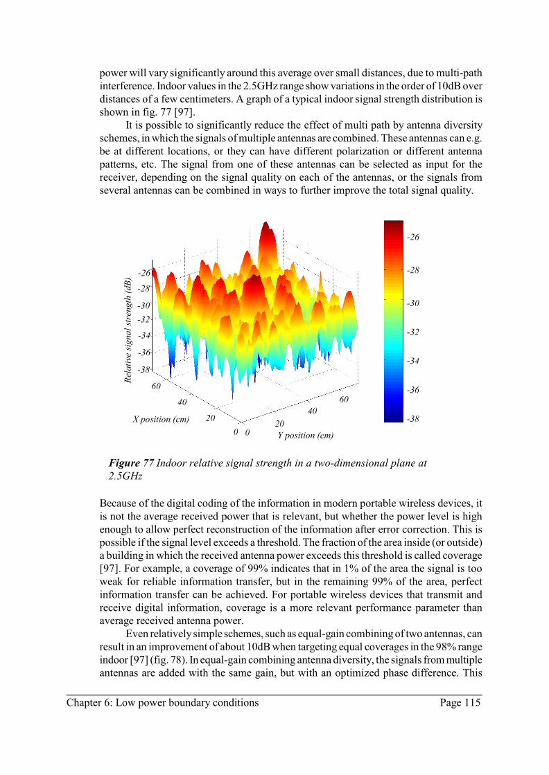
Chapter 6: Low power boundary conditions Page 115
Figure 77 Indoor relative signal strength in a two-dimensional plane at2.5GHz
power will vary significantly around this average over small distances, due to multi-pathinterference. Indoor values in the 2.5GHz range show variations in the order of 10dB overdistances of a few centimeters. A graph of a typical indoor signal strength distribution isshown in fig. 77 [97].
It is possible to significantly reduce the effect of multi path by antenna diversityschemes, in which the signals of multiple antennas are combined. These antennas can e.g.be at different locations, or they can have different polarization or different antennapatterns, etc. The signal from one of these antennas can be selected as input for thereceiver, depending on the signal quality on each of the antennas, or the signals fromseveral antennas can be combined in ways to further improve the total signal quality.
Because of the digital coding of the information in modern portable wireless devices, itis not the average received power that is relevant, but whether the power level is highenough to allow perfect reconstruction of the information after error correction. This ispossible if the signal level exceeds a threshold. The fraction of the area inside (or outside)a building in which the received antenna power exceeds this threshold is called coverage[97]. For example, a coverage of 99% indicates that in 1% of the area the signal is tooweak for reliable information transfer, but in the remaining 99% of the area, perfectinformation transfer can be achieved. For portable wireless devices that transmit andreceive digital information, coverage is a more relevant performance parameter thanaverage received antenna power.
Even relatively simple schemes, such as equal-gain combining of two antennas, canresult in an improvement of about 10dB when targeting equal coverages in the 98% rangeindoor [97] (fig. 78). In equal-gain combining antenna diversity, the signals from multipleantennas are added with the same gain, but with an optimized phase difference. This

Page 116 Chapter 6: Low power boundary conditions
Figure 78 Coverage of single-antenna and dual-antenna equal-gain and angle-scanning diversity
Figure 79 Equal-gain combiningconcept
concept is shown in fig. 79. In angle-scanning diversity, the same approach is taken, butthe optimized phase difference is determined periodically by scanning all possiblesettings of the phase difference. For speeds up to 5km/h and update frequencies of 1kHz,angle scanning performs as well as ideal equal-gain combining. Angle-scanning diversityhas been patented [112].
One way to interpret the function of an equal-gain combiner is to model the output signalfrom the adder as if it was generated by a single antenna with a complex antenna pattern.In that case, the effective antenna pattern of this virtual antenna depends on the value ofthe variable phase shifter. Fig. 80 demonstrates some of the antenna patterns that can begenerated in this way.

It is possible to implement advanced antenna diversity schemes on both sides of the radio link.7
Implementing diversity on one side of the link results in link budget improvements because of the antenna gain
created by multiple antennas, and because of the suppression of multipath fading. Adding antenna diversity on
the other side of a radio link as well will give additional antenna gain. The improvement because of the further
suppression of multipath is, however, typically negligible. Therefore, adding diversity on the other side of a
radio link will probably further improve the link budget by only about 3dB rather than another 10dB.
Chapter 6: Low power boundary conditions Page 117
Figure 80 Effective antenna patterns for different settings of the phaseshifter [97]
The approximately 10dB of link budget improvement that can be achieved with equalgain combining on one side of the radio link can be used to increase coverage and range.7
However, it can also be used to reduce the power dissipation of a system, whilemaintaining the original coverage and range. For example, the transmit power can bereduced by 5dB and the receiver sensitivity by the “other” 5dB. In this way,approximately 3x power dissipation reduction can be achieved both in transmit andreceive mode if the power savings are implemented on both transceivers in a link. Aneven larger power dissipation reduction can be achieved in asymmetrical systems, byreducing both the transmit power and receiver sensitivity by 10dB.
Figure 78 shows that the improvement depends on the target coverage. For highercoverage targets, the improvement is substantially more than 10dB. In figure 81, therelative power dissipation of the receiver is shown for both long-range and short-rangeapplications, assuming that half of the improvement in link budget is allocated toreducing transmit power, and the other half to reducing receiver sensitivity.Complementary to the situation with antenna losses, the increased signal levels providedby antenna diversity can be used to optimize the front end for a proportionally increasednoise figure and proportionally decreased gain, to maintain overall sensitivity and signallevels. In addition, the input IP3 of long-range systems has to increase proportionally tothe signal levels to maintain overall linearity. The result is shown in fig. 81. In this figure,the relative power dissipation is the power dissipation of a receiver with equal-gain

Page 118 Chapter 6: Low power boundary conditions
Figure 81 Relative power dissipation of long-rangeand short-range systems with equal-gain antennadiversity versus coverage. A power dissipation of100% corresponds to no antenna diversity.
antenna diversity relative to a receiver without antenna diversity. A short-range systembenefits more from antenna diversity, since there is no penalty (in terms of linearity) indealing with the larger combined signals, whereas in a long-range system extra linearityis required for dealing with larger signal levels. The situation for long-range systems canbe improved by using a diversity control algorithm that reduces interfering signals. Thiscan be achieved by optimizing for a trade-off between received antenna power of thewanted signal and suppression of unwanted signals. The impact of such a schemedepends on the amount of interferers that can be expected, and is an area that needsfurther research.
In this simple model, the power dissipation of the overhead circuitry needed toimplement antenna diversity has not been taken into account. In principle, the diversitycombination can be carried out by passive components between the antennas and thereceiver, without any additional signal-processing circuits. Also, with the predicted powerdissipation savings of 2.5 to 30 times for this example, there would still be appreciablepower savings in the brute force approach of doubling the complete receiver circuit.
6.1.6 Antenna interface lossesWhereas antenna gain helps to reduce power dissipation, any loss in the interface to theantenna increases power dissipation. Such a loss has to be compensated for by an equaldecrease in noise figure of the front end, in order to maintain the same overall noisefigure (and therefore sensitivity). The decrease in input IP3 requirements of the front endis offset by an identical increase of the gain requirements. Typical losses in the antennainterface include losses in the antenna filter, duplexer and/or switches, and can add up toabout 2dB or more.
Using again the DECT front end as an example, the effect of antenna interfacelosses on power dissipation can be estimated using the FAT tool. The result is shown in

Chapter 6: Low power boundary conditions Page 119
Figure 82 The effect of antenna interface losses onthe power dissipation of the DECT front end
fig. 82.
6.2 Circuit
In the design method described in the previous chapter, the performance of individualcircuits was considered a boundary condition. The design method focused only onselecting the “best” circuit. In this section, the design of circuits that are optimized forlow-power operation will be investigated.
Circuits for short-range systems operate at very high frequencies, close to the limitsof the IC process. Therefore, the most effective circuit topologies are typically verysimple. New low power circuit topologies, other than the scaling mentioned in thissection, are not likely to be used for short-range systems. Circuits for long-range systemsdo benefit from improvements in technology, because the RF frequencies for thesesystems will remain limited to the region below approximately 5GHz. Therefore, themargin between required circuit performance and available technology performance willincrease for these type of systems, and creative circuit topologies are more likely.
6.2.1 Circuits for short-range systemsIn short-range, high-bandwidth systems, the current required to achieve sufficient gainat high frequencies usually results in higher linearities than needed. Therefore, the mainproblem will be in designing circuits with sufficient gain at high frequencies, and withlow power dissipation. This can be achieved by reducing currents in the circuits (toreduce the power) while decreasing transistor sizes (to keep the available bandwidthconstant), and increasing impedance levels proportionally to the current (to keep the gainconstant), using OSIT_1 as the appropriate transform.
0 The characteristic impedance Z of a microstrip line on a PCB can be approximated by the impedance8
of a cylinder with diameter d above an infinite ground plane at distance D, in an environment with dielectric
r 0 rconstant e : Z = 138/%e log(D/d). Because of technological constraints, such as minimum track widths and
maximum via heights, D/d cannot be made very large. This limits the characteristic impedance to a few hundred
Ohms in practice.
Page 120 Chapter 6: Low power boundary conditions
This approach is often limited by technology that does not allow further scaling ofthe transistors and impedances with proportionally scaled parasitics. In that case,parasitics of transistors, passive devices and/or interconnect start to dominate theachievable gain at the desired signal frequency. A technology that can scale much furthertowards small devices and low currents, called silicon-on-anything, will be discussed inthe next section. Using such a technology, currents can be scaled down to the point wherethe linearity is just good enough, and further power savings will then require approachessimilar to those for long-range systems as discussed in the second part of this section. Theresult of this approach is a circuit with high internal impedance levels.
Circuits with high internal impedance levels are often difficult to interface toexternal signals and components, since the characteristic impedance levels on a PCB tendto be limited to a few hundred Ohms for practical reasons . This makes interfacing with8
the outside world awkward, and is an additional impetus for highly integratedtransceivers with a minimum number of interfaces to the outside world. At theseinterfaces, the impedance of the signals has to be adjusted to external impedance levelseither electronically or by passive components. Electronic matching will result inincreased power dissipation as well as additional noise and distortion. Matching throughpassive components that are on-chip is costly because of the required chip area, and if theon-chip passive components are of limited quality (as e.g. on-chip inductors often are)signal losses are incurred. Matching through passive off-chip components is mostcommon, but results in a higher overall component count. A better result could beachieved with a low cost IC technology that allows integration of high quality passivecomponents. Fortunately, silicon-on-anything also offers high quality passive devices atlow cost. An alternative solution would be the use of an optimized passive integrationtechnology specifically for the input and output matching. Within PhilipsSemiconductors, such technologies are available, e.g. Passi, PICS, COSIP etc.
6.2.2 Circuits for long-range systemsLow-power circuits for long-range systems need to meet three main design goals:C low noise figures at high frequenciesC good power/linearity (6) values at high frequencies C efficient output power generation
The noise figure is mostly limited by the properties of the active device and theavailability of high-quality passive components for the matching networks. Goodpower/linearity (6) values require high gain and/or good linearity at high frequencies andlow currents. One way of achieving this is through distortion cancellation (cf. SITs,Section 5.3.1). In principle, a perfect cancellation can be obtained for a single distortioncomponent. In practice, the reduction is limited by the matching that can be achievedbetween the branches. By recursively applying this procedure, in principle all distortioncomponents can be eliminated. Obviously, this is impractical for more than two or threecomponents because of cost, power dissipation, and accuracy of the circuits involved.

Chapter 6: Low power boundary conditions Page 121
Figure 83 Class-A/B emitterfollower
In order to achieve good linearity, many RF front end circuits operate in class A.The efficiency of the generated output power for class-A circuits is rather poor. Even atmaximum output levels it does not exceed 25% for a resistive load. The lowest signallevels in a front end are often five to eight orders of magnitude lower than the maximumsignals, resulting in efficiencies as low as 25 10 for such signals. Achieving better-10
power efficiency for low signal levels requires circuit topologies with power dissipationthat adapts to the signal levels, for example class-A/B outputs or class-A circuits withadaptive biasing, dependent on the signal levels. B. Gilbert has introduced a mixerstructure, called the “micromixer”, that depends on a class-A/B balun in the bottom stage[98]. Also, emitter followers with class-A/B behavior are well-known, e.g. the topologyin figure 83. These are examples of a trend towards more complex RF circuits for long-range systems, that take advantage of the increasing margin between required circuitperformance and available technology performance.
In the circuit of fig. 83, Q1 is the actual emitter follower. The biasing for Q1 is providedby Q2. The current through Q1 is sensed by Rcol. A feedback loop, consisting of Q4, Rls,and Q3, counteracts fluctuations of the current through Q1 by modulating the currentsource Q2. If the current through Q1 becomes smaller, the collector voltage rises. Thisrise in voltage is applied to the base of Q2 through the level shifter consisting of Q4 andRls. This increase in base voltage is translated into a higher collector current of Q2, andtherefore an increase in bias current for Q1. The voltage drop in the level shifter isdetermined by the bias current through Q3, and therefore by Vbias. Vbias also sets thequiescent current through the emitter follower. The modulation of the tail currentprovided by Q2 causes the class-A/B operation. It reduces current fluctuations in Q2,resulting in higher AC current gain of the emitter follower, and therefore higher input

Page 122 Chapter 6: Low power boundary conditions
Figure 84 Class-A/B differential pair
impedance, lower output impedance, and less distortion. Unfortunately, the circuit isasymmetric, in that the current of the current source Q2 can never be negative. Therefore,if more output current is required than can be provided by the quiescent current of thedevice, the tail current in Q2 switches off, and the current through Q1 starts to changewith the output current. The second-order distortion caused by this effect can besuppressed by using two of these emitter followers in balanced circuits.
Although the micromixer and the class-A/B differential pair provide useful buildingblocks for RF class-AB front ends, it is not yet practical to build a complete class-ABfront end. Most RF class-A circuits are balanced circuits, because they offer better secondorder distortion, better power supply rejection, and because they generate lessinterference for other circuits. Class-AB circuits should preferably be balanced as well,for the same reasons. In addition, class-AB circuits will generate variable supply currents,which can generate significantly more interference in other circuits than the constantsupply currents of a class-A circuit. This effect can be reduced by using balanced class-AB circuits, that reduce especially the supply current variations at the signal frequencies.What is left is supply current variations at double the signal frequencies, but these areoften easier to deal with. The main missing circuit type is therefore a class-AB balancedamplifier, equivalent to a differential pair. Such a balanced gain stage could beconstructed from two input stages of the micromixer, since one input stage converts asingle-ended signal into a balanced signal. Using two such circuits with the outputs cross-coupled allows differential-input, differential-output operation. However, this topologyhas no common mode rejection at all. As part of this thesis, the following differentialclass-A/B amplifier has been investigated (fig. 84).
In this amplifier, the transistors Q1 and Q2 form the actual differential pair. R5 and R6are degeneration resistors to improve linearity. The usual tail current source has beenreplaced by two independent tail current sources Q5 and Q10. They are driven bycollector-current sensing resistors Rc1 and Rc2, through level shifters created by Q11 and

Chapter 6: Low power boundary conditions Page 123
Figure 85 DC transfer curves of the class-A/B differential pair: thetop graph shows the single ended output voltages versusdifferential input voltage. The bottom graph shows the differentialoutput voltage versus differential input voltage.
Q12 in combination with Re1 and Re2. These feedback loops again counteract anychanges in collector current of the input devices Q1 and Q2. In the class-A region, thecurrent that is needed to compensate these differences in collector current is exactlyidentical to the current through R5 and R6. This difference current is mirrored throughQ13 and Q14 to the outputs. By increasing the size of Q13 and Q14 compared to thecurrent sources Q5 and Q10, additional power gain can be implemented.
In the upper graph of fig. 85, the individual output signals are shown as a function of thedifferential voltage across the input. Only in a small region around zero, both outputs areactive and the circuit operates in class A. For input signal levels above 30mV, one outputsaturates and the other output continues. This provides a much higher compression pointthan would be possible with a class-A circuit and the same quiescent current. The lowergraph of fig. 85 shows the differential output signals as a function of the differentialvoltage across the input. The higher gain in the class-A region is clearly visible in thecenter of this graph.
The modulation of the power supply current is shown in fig. 86, showing areduction by more than a factor of 2. The small signal linearity is higher than the linearityof a class-A differential pair with the same quiescent current, since the feedback loopsand output stages act as a translinear circuit that compensates for the exponentialbehavior of the transistors. However, there is still a significant distortion in the transitionfrom class-A to class-B operation, since the saturation of one side of the circuit reducesthe gain by approximately a factor of two. This differential pair is very useful insituations where it is necessary to occasionally deal with strong single-tone interferers.In the absence of such interferers, the circuit operates at low currents in class A, and ishighly linear. When such interferers are present, the circuit switches instantaneously intoclass-A/B operation, and avoids the signal deterioration caused by the limiting that occursin class-A circuits with low biasing and therefore low compression points.

Page 124 Chapter 6: Low power boundary conditions
Figure 86 The top graph shows the differential output voltageversus the differential input voltage of a class-AB differential pair.The bottom graph shows the supply current versus the differentialinput voltage of the same circuit.
This circuit can be the basis for a full class-A/B front end. It does require sufficient gainat high frequencies and low quiescent currents for the control loops, and is thereforesuited for the same type of IC processes required for low-power, short-range circuits. Thisclass-AB differential pair has been patented [111].
6.3 Technology
The power consumption of an RF circuit depends, among others, on the properties of thedevices in the circuit, and therefore on the technology used to implement them. Theinsights derived from the minimum power design method of Chapter 5 can be used toidentify the properties that limit a further reduction of the power dissipation of RFcircuits. This can be used as a basis for developing new technologies that are optimizedfor low power RF circuits.
To quantify the properties of devices and IC processes that affect the powerdissipation of RF front-end circuits, various methods can be used, including:C design, fabrication and measurement of benchmark circuitsC coupled device and circuit simulation [99]C circuit simulationC figures of merit (FOMs)FOMs are an attractive and popular method, because they give a quick indication of theproperties of a device and/or process, and can be calculated with a minimum amount ofeffort. Moreover, they allow for a very straightforward analysis of the factors in a deviceand/or process that can be changed to improve the results.

Chapter 6: Low power boundary conditions Page 125
(78)
(79)
(80)
6.3.1 A new FOM for the gain of active devicesFor short-range systems, the main performance criterium for the active device is gain athigh frequencies and for low currents. For long-range systems, the performance criteriumshould also include linearity. In this subsection, a new FOM for short-range systems willbe introduced, and in the next subsection this will be extended to an EFOM that isrelevant for long-range systems.
T.The figure of merit for the bandwidth of active devices is currently still f , the(extrapolated) frequency at which the current gain of a transistor is reduced to unity.
TUnfortunately, f is a very poor indicator for the performance of low power RF circuits
T[110]. The main shortcoming is that f neglects several significant parasitic effects in a
Tdevice because of the transistor configuration for which f is relevant is not representative
Tfor a typical RF circuit. The only configuration for which f accurately predicts the unitygain bandwidth would be a common emitter stage in which the output of the device isshorted, and the input is driven by an ideal current source. In low power RF circuits, suchconfigurations are not used. Another currently popular figure of merit for active device
max maxbandwidths is f . However, f is not a very relevant FOM for most RF circuits either,since it requires perfect power matching at the input and output of the device. Since theinput and output impedances of active devices at these frequencies are partiallycapacitive, a matching circuit requires inductors. In most IC technologies, inductors havea limited quality factor, and their large physical size makes them expensive. Therefore,most on-chip RF circuits don’t use power matching, and require other figures of merit.
A new figure of merit should represent the bandwidth of a common emitterconfiguration with resistive load and significant gain at low currents. Therefore, the gainof such a configuration versus current and frequency will be discussed first. At lowfrequencies, the gain of a bipolar transistor is typically limited by the voltage drop across
ethe parasitic emitter resistance R , that reduces the effective transconductance:
min which g is the transconductance of an ideal bipolar transistor:
cwith q the electron charge, k the Boltzman constant, T the absolute temperature, and Ithe collector current of the active device. Another limitation for the voltage gain is the
lmaximum value of the collector load resistor R :

Page 126 Chapter 6: Low power boundary conditions
(81)
(82)
(83)
cc ce,minin which V is the power supply voltage, V the minimum collector-emitter voltage
c lof the device, and I the collector current. This value of R is often not practical, since it
l l,maxonly applies to very small signal levels. A more typical value of R would be ½ R ,since this allows for maximum output signal levels. The maximum voltage gain that canbe achieved by this active device can be found by combining (78) with (80):
The only parameter in (81) which is significantly influenced by the device and process
e ce ccproperties is R . The variation of V is often negligible compared to V . It might seem
ethat R is therefore a good indication of the low frequency gain performance of a
c etransistor. However, only the product I R affects the gain - one is meaningless withoutthe other. The effect of parasitic emitter resistance can be reduced by running the
v,maxtransistor at very low currents. This is already included in G (0).In general, the bandwidth of a common emitter stage is limited by a combination
of at least 7 and possibly as many as 24 time constants [104]. In low power RFapplications, two of them are dominant in most devices and processes. One time constantlimits the frequencies that can get into the intrinsic transistor from the outside (input timeconstant), and another time constant limits the frequencies which can get out of thetransistor (output time constant):
1C The output time constant consists of the external load resistor R and the collector-
jc jsbase (C ) and collector-substrate (C ) capacitor of the active device. This results in
outa definition (82) for the output bandwidth f : the frequency at which the voltage gain
v vG has decreased by 3dB from an initial value G (0).
outIt is conventional to define f for a low voltage gain of 10, since this is a typicalvalue for the input stage of a low noise amplifier (83). Note that the output bandwidthincreases with increasing collector current.
bC The input time constant consists of the base resistance R and a combination of base-
je Demitter junction capacitance C , diffusion capacitance C , and the Miller-enlarged
jccollector base junction capacitance C . As a first approximation, the effective baseresistance is assumed to be lumped in series, and all capacitors are assumed to be

Chapter 6: Low power boundary conditions Page 127
(84)
(85)
Figure 87 Voltage gain as a function offrequency
vconnected in parallel. Using this simple model, the input bandwidth f is defined asthe frequency at which the gain of a common emitter stage with has dropped by 3dB
(84):
With the usual assumption of Gv(0)=10, this becomes:
Note that the input bandwidth decreases when the collector current of the device
Dincreases, because C increases with the collector current.
vThe expression for f does not take into account the effects of the parasitic emitterresistor. This resistor serves as a feedback across the first gain stage, reducing the low-frequency gain, and increasing the input bandwidth by the same amount. This increased
v v,max v v outbandwidth is indicated by the symbol f ’. The combined effect of G (0), f , f ’, and fon the gain and bandwidth behavior of a bipolar CE stage is shown in fig. 87 for the case
out vwhere f exceeds f ’:
v outWhether f exceeds f or the other way around depends on the biasing of the transistor.In fact, a biasing condition exists at which the total bandwidth of the circuit is optimized:higher currents would reduce the input bandwidth, and smaller currents would reduce theoutput bandwidth. By extending fig. 87 to include the collector current as an independentvariable, this optimum biasing point can be made visible. In fig. 88, such a graph isshown for a common emitter stage with a minimum size NPN device in the QUBiCprocess [102]. In this case, it is obvious that for biasing currents lower than the collector
Tcurrent for peak f , no optimum bandwidth: is found: increasing the collector currentresults in a continuously increasing bandwidth. This is also consistent with the experience

Page 128 Chapter 6: Low power boundary conditions
Figure 88 Gain of a QUBiC1 CE stage versusfrequency and current
Figure 89 Gain versus frequency and biasingfor a minimum size QUBiC1 NPN device, with
jsC reduced by 90%
of many RF designers: “if you want higher frequencies, you need to spend more current”.
outThe difference between fig. 88 and fig. 87 is caused by the relatively low f of this
v outdevice: f (1.6GHz) still exceeds f (1.2GHz) for the highest biasing condition.
outTherefore, performance is limited mainly by f . To obtain better performance from this
outcircuit, the device should be optimized to improve the parameters that make up f , i.e.
js jc js jcC and C . In this case, the value of C is much larger than the value of C . This is rather
jstypical for many small bipolar RF devices, and can be solved by reducing Csignificantly, e.g. through trenches, such as in QUBiC4. The gain for such a device isshown in fig. 89. In this graph, an optimum biasing condition at high frequencies caneasily be identified.
T TRF IC processes are often characterized by their f . However, f as a FOM for RF low-
out vpower performance is not very relevant, since f and f do not depend significantly on

Chapter 6: Low power boundary conditions Page 129
Figure 90 Voltage gain as a function offrequency and current, of a minimum size NPN
Tin QUBiC1 with f twice the original value
T. Tf This is further illustrated by comparing fig. 88 to fig. 90, in which the f of thetransistor has been doubled compared to fig. 88 without any obvious effect on the high-
Tfrequency gain of the device. The negligible impact of f on the gain can be explained bythe dominant time constants formed by relevant parasitic elements of the transistor, such
Tas the base resistance and the collector-substrate capacitance, that are neglected by f .
out TTherefore, optimizing the next QUBiC generations for f rather than for f is much morerelevant for low power RF circuits. With the trenches in QUBiC4, this is indeed thedirection that the technology is now developing.
The total bandwidth of the active device is sometimes defined by the figure of merit
a vf . The bandwidth of a common emitter stage with resistive collector load such that G (0)
a a v=10 is defined as the available bandwidth f . In this way, f combines the effects of f and
outf in a single FOM. While the output bandwidth of most devices was dominated by the collector-
out asubstrate capacitance, f and f provided adequate indications of the RF performancelimits of active devices. With new technologies, such as the trenches in QUBiC4, thatsignificantly reduce the collector-substrate capacitance, this is no longer true, and a newFOM is needed. The bandwidth of a common emitter stage in an RF circuit is nowsignificantly affected by the load of the next stage. This load depends of course on thespecific design in which the common emitter stage is used. In some cases, it will be anemitter follower which provides a relatively low load to the CE stage, in other cases itwill be another CE stage with a larger device and larger currents. As with the choice of
v outG (0) for f , a typical situation can be defined. In this case, such a typical situation is theloading of the CE stage by an identical CE stage, which provides a load somewherebetween the two cases mentioned before. This results in a new FOM which will be named
coll collthe collector bandwidth f in this thesis. The corresponding expression for f is givenby (86).

Page 130 Chapter 6: Low power boundary conditions
(86)
(87)
(88)
(89)
The input bandwidth is not significantly affected by the loading of the next stage.
aSimilar to the definition of the available bandwidth f of an unloaded common emitterstage, another new FOM is defined here which represents the bandwidth of a loadedcommon emitter stage as the combined input bandwidth and the collector bandwidth. It
lis named the loaded bandwidth f . This FOM is relevant when comparing moderntechnologies that use trenches or other techniques to reduce the parasitic capacitance atthe output of the active device, especially the implementation of circuits for short-rangesystems.
l coll DFor low currents, f is dominated by f , and C will become negligible compared
js jc je m eto the other capacitances in the denominator (C , C , and C ). Also, the term g R will
lbecome negligible. Therefore, at low currents, f can be approximated by (87).
lThis bandwidth is proportional to the current. Therefore, the ratio between f and thecollector current is a good measure for the bandwidths that an active device can achieveat low currents, and will be called the bandwidth-current ratio or BCR (88, 89, 89).
vWith the usual assumption G (0) = 10, this becomes:
6.3.2 An EFOM for active devicesFor long-range systems, BCR is not a sufficient indication for the low power limits of adevice, since it does not take into account the linearity requirements of these systems.Another FOM is needed for this purpose, and can be based on the EFOM_1 that wasintroduced in Section 5.4. Since the EFOM_1 is valid for any two-port circuit, it can beapplied to active devices in a two-port configuration:

Chapter 6: Low power boundary conditions Page 131
(90)
(91)
l cAt low currents, the term f / I can be replaced by BCR. Together with the usual
vassumption of G (0) = 10, EFOM_1 for active devices can be rewritten as:
The EFOM_1 value can be improved by the BCR. This has the additional advantagethat the device becomes more attractive for both short-range and long-range systems. Interms of the FOMs discussed in the previous sections, this can be achieved by improving
coll je jc jsthe f , which, in turn, can be achieved by reducing the C , C and C of the active
D Tdevice. Note that the diffusion capacitance C , and therefore the f , does not appear in theexpression for BCR, and is therefore not relevant for the low-power, high-frequencyperformance of active devices in either short-range or long-range systems.
6.3.3 Influence of passive devicesWith so much emphasis on active devices, both in the previous sections and in literaturein general, it is easy to forget that other parts of an IC also affect the RF performance. Incircuit simulators, bipolar transistors are often described in excruciating detail, using e.g.more than 50 parameters to describe a single transistor in the Mextram model. Parasiticeffects of passive components, IC substrate, interconnect and package parasitics get muchless attention, and are sometimes completely ignored, even though they can have asignificant impact on the performance of high-frequency, low-power circuits [103]:C In the DECT LNA, simulations indicate that the 15:m-long track of minimum-width
bottom metal at the collector of the input transistor, reduces the bandwidth of thiscircuit by 10%.
C Metal plate capacitors are often required to achieve sufficiently high quality factors,but these capacitors can have up to 50% of their nominal value as parasiticcapacitance to the substrate.
C Inductors in typical BiCMOS processes achieve quality factors of 10 or less, makingthem rather useless for low-noise oscillators or narrow-band filters. For a very low
ccvoltage LNA circuit (e.g. V =1V), higher quality inductors would be very useful tocompensate collector-substrate capacitances and achieve power matching.
C Crosstalk between different parts of the circuit through interconnect and substratecoupling are becoming more and more a cause of performance problems in high-frequency circuits.
C A combination of bondwire inductance (several nH), bondpad capacitance (about1pF) and ESD protection diode capacitance (around 1pF) can have resonancefrequencies around 2GHz, upsetting input matching and gain characteristics of high-frequency ICs.

Page 132 Chapter 6: Low power boundary conditions
Figure 91 Relative capacitance versus width/height ratio ofinterconnect lines
C In some circuits, such as the DECT front end, crosstalk is already limited by theinductive coupling of the bondwires of the IC package.
The importance of these effects typically increases with frequency and impedance level.Therefore, these effects will be particularly relevant for future high-frequency low-powercircuits. Also, many of these effects don’t scale with device improvements, and specialapproaches might be required to deal with them. The process discussed in Section 6.3.4also addresses high-quality passive components.
6.3.4 An optimized low-power IC process: Silicon on AnythingTo achieve very high output bandwidths at low currents, the capacitance from collectorto substrate should be reduced drastically. At the same time, the capacitance of theinterconnect needs to be reduced as well, in order to allow for the higher impedancelevels in the circuits. There are two ways in which the capacitance of interconnect can bereduced: 1. By reducing the dielectric constant of the material between the interconnect and
the ground;2. By increasing the distance of the interconnect to the ground relative to the line
width of the interconnect.
2The first approach is limited, since the relative dielectric constant of SiO , the mostcommon inter metal dielectric, is around 4. A decrease to values around 2 is possibleusing low-k dielectric materials, but significant further improvements are unlikely. Thesecond approach is limited, because the capacitance of interconnect will no longer scaleproportionally once the width of the interconnect becomes much smaller than its heightover the substrate. This effect is shown in fig. 91.
The increase in oxide thickness that would be required to achieve an interconnectcapacitance reduction by an order of magnitude is very impractical using standard IC-processing techniques. Therefore, a different approach is needed.
Both the scaled transistor and scaled interconnect parasitics have been addressedsimultaneously in the Silicon-on-Anything (SOA) process [106]. This is a bipolar ICprocess in which the active layer of an (upside-down) SOI wafer is glued onto a substrateof choice (the “anything”) after processing, as shown in fig. 92.
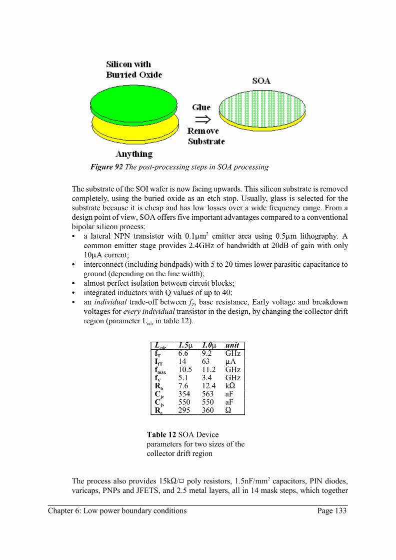
Chapter 6: Low power boundary conditions Page 133
Figure 92 The post-processing steps in SOA processing
cdrL 1.5: 1.0: unitTf 6.6 9.2 GHzfTI 14 63 :Amaxf 10.5 11.2 GHzVf 5.1 3.4 GHz
bR 7.6 12.4 kSjcC 354 563 aFjsC 550 550 aFeR 295 360 S
Table 12 SOA Deviceparameters for two sizes of thecollector drift region
The substrate of the SOI wafer is now facing upwards. This silicon substrate is removedcompletely, using the buried oxide as an etch stop. Usually, glass is selected for thesubstrate because it is cheap and has low losses over a wide frequency range. From adesign point of view, SOA offers five important advantages compared to a conventionalbipolar silicon process:C a lateral NPN transistor with 0.1:m emitter area using 0.5:m lithography. A2
common emitter stage provides 2.4GHz of bandwidth at 20dB of gain with only10:A current;
C interconnect (including bondpads) with 5 to 20 times lower parasitic capacitance toground (depending on the line width);
C almost perfect isolation between circuit blocks;C integrated inductors with Q values of up to 40;
TC an individual trade-off between f , base resistance, Early voltage and breakdownvoltages for every individual transistor in the design, by changing the collector drift
cdrregion (parameter L in table 12).
The process also provides 15kS/9 poly resistors, 1.5nF/mm capacitors, PIN diodes,2
varicaps, PNPs and JFETS, and 2.5 metal layers, all in 14 mask steps, which together

Page 134 Chapter 6: Low power boundary conditions
Figure 93 Cross section of an SOA transistor
Figure 94 Available common emitter bandwidth (fa) versuscollector current for a minimum transistor in SOA and in QUBiC1
with the 0.5: lithography results in low fabrication costs. This allows cost-efficientintegration of high performance input and output matching circuits. Fig. 93 shows thelayout and cross section of an SOA transistor connected to a polysilicon resistor.
To demonstrate that the goal of increasing gain at low power levels has been achieved in
athe SOA process, figure 94 shows the f of both a minimum-size SOA transistor and astandard 1:m QUBiC1 transistor.
The high bandwidth at low currents is a direct result of the scaling of the emitter area andproportional scaling of the transistor parasitics, enabled by the fully isolating substrate.The difference between the processes is also clearly captured by the newly introduced

Chapter 6: Low power boundary conditions Page 135
FOM and EFOM_1 for active devices in this chapter, as shown in table 13. The BCRindicates about 20 times better low power performance of the SOA process compared toQUBiC1, and the EFOM_1 for active devices indicates an almost 2x better performanceof the SOA process compared to QUBiC1. In other words: the SOA process is more thanone order of magnitude better for short-range systems, and almost a factor of 2 better forlong-range systems. This is consistent with the experience of designers who havedesigned circuits in this process: low power high frequency circuits work extremely well,but the advantage for circuits that need higher currents to achieve the required linearityis not nearly as big.
SOA QUBiC1
BCR 126MHz/:A 5.32MHz/:A
EFOM_1 293MHz 177MHz
Table 95 BCR and EFOM_1 figures of merit for SOA and QUBiC1 processes
These active devices, together with the enhanced passives and low-parasitic interconnectmake SOA an ideal technology for low power RF design, especially for short-rangesystems.
6.4 Summary and conclusions
The minimum power design method that was introduced in Chapter 5 is, in addition tobeing useful as the basis for a design procedure, also a good basis for identifying thelimits for further power dissipation reduction at the system, circuit and technology levels.At the system level, significant improvements are possible through advanced antennadiversity schemes. By using the extra margin in the link budget that is created byadvanced antenna diversity for relaxing the requirements of the transmitter and receiver,the power dissipation of a system can be reduced by factors of 2 to 20, depending on thesystem.
At the circuit level, scaling to high impedance levels using OSIT_1 provides themost promising approach for short-range systems. Long-range systems, on the other hand,will benefit from an increasing margin between circuit requirements and technologyperformance. This increased margin can be used to reduce the power dissipation by moreelaborate circuits than before. In time, RF circuit design for this type of system is likelyto develop in the direction of analog/mixed-signal type of circuits. The first steps in thisdirection are already visible in class-AB circuits. In this section, a new class-ABdifferential amplifier has been introduced.
A convenient way of analyzing the requirements for new technologies is throughFOMs, especially for active devices. A new FOM for active devices, named bandwidth-current ratio (BCR), has been introduced, which is relevant for low power RF circuits,especially in short-range systems. This FOM has then been extended to an EFOM_1 foractive devices, which is relevant especially for long-range systems. The BCR has beenused to identify the device parameters that are limiting further power reduction of RF

Page 136 Chapter 6: Low power boundary conditions
js jc jecircuits in both system types. The junction capacitances C , C and C are the dominantparameters for BCR. The diffusion capacitance does not have a significant influence,
Twhich confirms the lack of relevance of f as a FOM for low power RF circuits.A new technology, called Silicon-on-Anything (SOA), offers exactly the
improvements in BCR identified in this chapter. In addition to these optimized activedevices, SOA offers the high quality passive devices and low-parasitic interconnectneeded to build complete low power RF circuits. A comparison of BCR and EFOM_1numbers between SOA and QUBiC1 shows an advantage of more than one order ofmagnitude for short-range systems, and a factor of about 2 for long-range systems. In themeantime, next generations of the QUBiC process family have been developed, butQUBiC1 is a relevant benchmark because of the comparable time frame, processcomplexity and cost of both processes.

This transceiver is not compatible with any of the IEEE 802.11 standards, even though it operates in9
the same 2.5GHz ISM frequency band as the IEEE 802.11b and IEEE 802.11g systems. The data rate of this
system is 100kbps, the transmit power 10dBm, and the modulation GFSK with BT=0.5.
Chapter 7: Low power front end circuits Page 137
Chapter
7Low-power front end circuits
Many of the concepts and ideas described in this thesis have been used in theimplementation of a new transceiver with very low power dissipation. Specifically, theOSIT_1 transform from Chapter 5 has been used to scale circuits to high impedancelevels and low currents. Also, power dissipation reduction based on angle-scanningdiversity, as described in Section 6.1, has been applied, as well as the short-range circuitoptimizations in Section 6.2. This circuit has been implemented in the silicon-on-anything (SOA) IC process (Section 6.3). In fact, it was the first circuit developed inSOA. It was instrumental in the definition and optimization of the process. Finally, theIF IC uses the resistive interpolation, multi-phase differentiate-and-cross-multiplydemodulation, and data reconstruction approach described in appendix E. The designmethod from chapter 5 was not completely developed yet at the time of this design,therefore only an early version could be has been used in this design. If the completedesign method had been available, the total power dissipation might have been evenlower than the results presented in this chapter!
The transceiver implements a proprietary WLAN radio at 2.5GHz, and can be9
classified as a short-range system (cf Section 1.1).

Page 138 Chapter 7: Low power front end circuits
7.1 Transceiver architecture
In a short-range system, the emphasis will be on achieving high bandwidths at lowcurrents, rather than on linearity. Therefore, an IC process is needed that allows scalingto high impedance levels for both the devices and the interconnect, as modeled by theOSIT_1 transform (Section 5.3). Obviously, SOA (Section 6.3.1) is the most appropriatetechnology choice. In fact, this circuit was the first complete transceiver designed in theSOA technology. Since, at that time, the SOA process was new and not yet fullystabilized, the design was partitioned into 4 separate dies to reduce the risk, and to allowfor easier testing. The partitioning chosen was:C receiver front endC VCO/synthesizerC IF circuits & demodulatorC power amplifierThis closely resembles the partitioning selected for the RF platforms approach, asdiscussed in the next section. One advantage of this partitioning is that there are relativelyfew RF interfaces between the different dies, reducing the need for input and outputbuffers at RF to drive off-chip interconnect. Only the connections from theVCO/synthesizer die to the power amplifier and receiver front end are actually runningat RF frequencies. A further partitioning into smaller circuits would have further reducedthe risk, and allowed for easier measurements, but the many RF interfaces would havecaused a significant increase in the power dissipation.
TSOA transistors have an f of less than 10GHz. The success of this 2.5GHz
Ttransceiver, at more than 25% of the f , demonstrates once more the lack of relevance of
Tf , at least for low-power RF front ends (Section 6.3). To further reduce the power dissipation, angle-scanning antenna diversity was
implemented, as described in Section 6.1. This improved the link budget by almost 10dB.These 10dB were traded for reductions in transmit power, sensitivity requirements, andinterfering signals, and to improve coverage. A GFSK modulation was chosen for thesystem. This allowed for non-linear processing of the signals at IF and in the demodulatorof the receiver, using interpolation and reconstruction as described in appendix E. GFSKalso enabled direct modulation of the VCO during transmit, eliminating the need for upconversion mixers.
For the design of a low-power receiver in SOA, two areas need special attention:C processing high dynamic range signals (weak signals and strong interferers)C interfacing to external circuitsProcessing high dynamic range RF signals is usually carried out in class A stages tominimize distortion, especially since the current for class-A operation is often neededanyway to achieve sufficient gain-bandwidth products. In SOA, gain-bandwidth productsof 25GHz are achieved at collector currents as low as 10:A. Angle-scanning diversityavoids having the power dissipation of most of the circuits dictated by the dynamic rangeof the antenna signals. In angle-scanning antenna diversity, the signals of a number ofantennas are first shifted in phase, and then added to form an effective antenna patternwith one or more beams and nulls. The beams increase the level of desired signals, and

Chapter 7: Low power front end circuits Page 139
Figure 95 Block diagram of the complete receiver
the nulls reduce the level of interferers. This is usually implemented by programmablephase shifters at RF, but they are difficult to implement at 2.5GHz.
In this design, a zero-IF architecture has been chosen. A block diagram of a dual-beam, equal-gain antenna diversity receiver is shown in fig. 95. The phase shifting iscarried out after the quadrature down conversion by adding weighted I and Q signals.Shifting the original signals I and Q over an angle N to obtain the phase-shifted signals
ps psI and Q is implemented as:
(92)
The weighting is accomplished through the 4 variable-gain amplifiers in fig. 95. Thesevariable-gain amplifiers are implemented as Gilbert cells, and are controlled by dual 8-bitDACs that generate the voltages corresponding to the cos(N) and sin(N) terms in eq. 92.
This method of phase shifting provides the highest flexibility, since the weighting factorscan be adjusted in very small steps, which is especially important for combinations of alarger number of antennas.
For two antennas, a simpler circuit is possible as well, using resistive interpolation(fig. 96). In this circuit, the I+ and I- signals are the balanced outputs of the “I” mixer in

Page 140 Chapter 7: Low power front end circuits
Figure 96 Diagram of the alternative, interpolation type, phase shifter
the zero-IF receiver, and the Q+ and Q- signals are the balanced outputs of the “Q” mixer.The resistive interpolation provides phase shifting in steps of B/4. Typically, this issufficient for a two-antenna, angle-scanning diversity system, but smaller steps can beimplemented easily by additional taps in the resistive divider. This divider is linked in adiamond across the four phases that come out of the balanced outputs of the two mixers.In the schematic, this is accomplished through the wire connecting the bottom of thelowest resistor with the top of the highest resistor. In a layout, a more symmetricalapproach can be achieved by folding the resistors. The series resistors of R, together withthe load resistors of (1+%2) R, provide an attenuation such that the output signal has thesame amplitude at every phase setting. These resistor values assume a voltage source andan infinite impedance load at the output, as well as zero “on” impedance of the NMOSswitch transistors. In practice, the resistor values need to be adjusted to take imperfectsource and load impedances, as well as realistic “on” impedance of the NMOS devices,into account.The gates of the NMOS devices are controlled by digital signals in such a way, that onlyone device out of every group of eight is switched “on”, and the other seven are switched“off”. Therefore, the output signal corresponds to the signal at one of the nodes of theresistive divider. This circuit provides one balanced pair of outputs. The second pair ofbalanced outputs needed in a zero-IF receiver can be created in a similar way, by addingtwo more groups of eight NMOS devices to the taps on the resistive divider.
Resistive dividers can also be used for diversity schemes with three or more antennas.However, such schemes typically use maximum ratio combining rather than equal gaincombining. For maximum ratio combining, both the amplitude and the phase of theindividual antennas needs to be adapted. This requires a two-dimensional resistivenetwork, which is more complicated to design and implement, especially if crosstalk and

Chapter 7: Low power front end circuits Page 141
parasitic phase errors need to be minimized. This implementation for angle-scanningantenna diversity, in which the phase-shifting is achieved through weighted addition ofquadrature IF signals has been patented [113].
Since MOS devices where not stable yet in SOA at the time of this design, a phaseshifter circuit with DACs and variable gain amplifiers was selected instead of this moresimple circuit.
7.2 Receiver front end
Interfacing to external circuits is complicated by the high impedance levels on chip, inthis design between 5kS and 50kS. The off-chip levels are, for practical reasons, around50S.This can be solved through passive LC-type transformers and/or electronic buffer stages.Since the first solution consumes a lot of die area, and the second a lot of current,reducing the number of external connections is very important for low-power RF ICs.This was one of the reasons to select a zero-IF architecture. Ultimately, the total receiverwould be implemented as a single IC. With the current partitioning, a simple receiver canbe built from 3 ICs: front end, IF, and VCO/synthesizer. A full dual-beam diversityreceiver consists of 2 front-end ICs, 2 IF ICs and 1 VCO/synthesizer IC. TheVCO/synthesizer IC is discussed in [83]. It consists of an LC oscillator at twice the RFfrequency, followed by a traveling wave divider that generates the quadrature signals, anda programmable divider chain.
The receiver front end has an RF input that uses a combination of LC circuits andelectronic buffers to achieve the required impedance transform. The schematic diagramof the LNA is shown in fig. 97. It is implemented with an integrated LC-type transformerthat feeds into a common-base stage with 300S input impedance. The common-basetransistors Q1 and Q2 each consist of 7 minimum transistors in parallel. Each minimum
11transistor is biased at 24:A. The measured s at the RF input is -12dB. The output of thecommon base stage is connected to two differential pairs which provide variable-gainoperation. These feed into the RF inputs of the mixers. The LNA provides 20dB of gainat 336:A with a 4dB noise figure and -20dBm IP3. The higher noise figure compared tomany other front ends is caused by the common-base input stage, but is acceptablebecause of the path loss improvement from the angle-scanning diversity. The common-base input stage helps to achieve good linearity performance at low currents.

Page 142 Chapter 7: Low power front end circuits
Figure 97 LNA Schematic
Figure 98 EFOM of SOA LNA in context of DECT and other LNAs from literature
When comparing this LNA with the LNA from the DECT front end from Chapter 4 andthe LNAs from literature as discussed in Section 2.1, the following EFOM values arefound (fig. 98).

Chapter 7: Low power front end circuits Page 143
Figure 99 IP3 Measurement result
As this graph shows, the low-power performance of this LNA is better than any otherLNA in this graph. The fact that such a good EFOM value is achieved at such a lowpower consumption level, namely 1mW, demonstrates how well SOA technology allowsthe scaling of circuits to low currents without affecting the EFOM value.
The OSIT_1 describes the scaling of linearity and current without affecting theEFOM value. Scaling upwards, i.e. increasing the current and linearity, is verystraightforward, and is accurately predicted by OSIT_1. Scaling downwards, to lowercurrents and linearities, is limited by the scaling properties of the technology used, asdiscussed in C. The high EFOM values at low currents that are achieved with SOA provethat this technology is capable of accurate scaling down to low currents, thanks to thesmall, lateral active devices, the high-quality passive components, and of course the low-parasitic interconnect.
The LO inputs are implemented with electronic buffers. In a single-chip version ofthis receiver, the LO will obviously be an internal connection which doesn’t need thesebuffers. The buffers are implemented as differential pairs and provide 8.5dB of gain. Themixers themselves are Gilbert cell topologies and provide 17dB of gain, whereas thephase shifters have a maximum gain of 0dB. The total die area of the front end IC is9mm , but a significant part is used for the digital control and DACs of the diversity2
circuits. The measured performance shows an overall gain of 35dB, with 6.2dB noisefigure and -22dBm IP3. The IP3 measurement result is shown in fig. 99.
The supply current of the total receiver front end is 1.0mA at 3.0V, with about half thatcurrent going into the LNA and mixers, and the other half into the DACs and phaseshifters, which can be powered down independently. Biasing is provided by on-chipbandgap reference sources. The complete die is shown in fig. 100. Although this die is“upside-down” after the substrate transfer, the devices are still visible because theoriginal substrate has been removed. The replacement glass substrate below the devices

Page 144 Chapter 7: Low power front end circuits
Figure 100 Die photo of the SOA WLAN front end
is transparent. This explains the shadows from the bondwires and large metal structuressuch as bondpads and inductors.

Chapter 7: Low power front end circuits Page 145
Figure 101 Reconstruction circuit
7.3 IF and demodulator
The IF IC (see fig. 95) consists of dual 4 order active lowpass filters, with a bandwidthth
of 100kHz, that provide channel selectivity. To fit a high-bit-rate signal into a frequency-modulated channel with a limited bandwidth, the frequency deviation is kept small, inthis case at approximately half the bit rate. Since this results in few zero-crossings of theIF signal for each bit, special attention is needed for non-linear processing in limiters anddemodulator.
As described in appendix E, this can be solved by creating multiple IF signals at differentphase offsets. Such additional IF signals can be created by resistive interpolation, in thesame way as the phase generation for the antenna diversity (fig. 96). In fact, the samecircuit could be used by adding extra switches. However, this would increase the numberof switches in the overall system. Also, additional channel filters would be required.Since this would consume additional power, and since the filtering and interpolation areboth linear operations, they can be done in a different order without affecting the result:first filtering, then interpolation.

Page 146 Chapter 7: Low power front end circuits
Figure 102 Signals in the reconstruction circuit
After the interpolation, limiters provide the high gain required to drive the demodulatorwith sufficiently large signals. They also eliminate any amplitude variation. The IFsignals are then converted to baseband information by a 4 branch differentiate-and-cross-multiply demodulator, as shown in fig. 162 in appendix E. The demodulator providespulses at 8 times the IF frequency, with positive pulses for positive frequencies andnegative pulses for negative frequencies. This is sufficient for a reliable detection of thedata. However, there will still be some jitter on the data transitions, so bit clock recoverymight be affected. This is corrected by a reconstruction circuit based on the

Chapter 7: Low power front end circuits Page 147
reconstruction algorithm of appendix E.This circuit is connected to the outputs of the differentiate-and-cross-multiply
demodulator. A schematic diagram of the reconstruction circuit is shown in fig. 101.Some of the signals in this circuit are shown in fig. 102. The purpose of this circuit is toshift the transitions of the demodulated data signal to the correct position, which is afixed offset in time after the time halfway in between the two adjacent pulses withopposite sign that caused the data transition. The principle of this circuit depends onmeasuring the time through the voltage of an integrator with a fixed input. By resettingthese integrators when a positive or negative pulse occurs, the time since the last positiveor negative pulse can be determined from the output voltages of the respectiveintegrators. Because the time intervals are represented by voltages, a voltage representinga moment in time halfway in between two pulses can be determined by taking the averageof the voltages representing the time intervals. Adding an offset in time can now berepresented by adding an offset voltage to the output of an integrator. The operation ofthe reconstruction circuit is described in more detail in the next paragraph.
The positive and negative pulses of the four-branch derivative and cross-multiplydemodulator are fed into the top part of the circuit. The demodulator output is shown as“Dem” in the signal diagram. In fact, the positive and negative pulses are providedseparately to individual inputs of the reconstruction circuit, labeled “Dem+” for thepositive pulses, and “Dem-” for the negative. In the top part of the circuit, two voltages<1 and <2 are created that are proportional to the desired variable time delay, which ishalf the time between successive opposite pulses. The signals “Dem+” and “Dem-”operate switches in parallel to capacitors with a value 2C. When a switch is closed by apulse, the voltage across the capacitor will be reset to 0V. After the switch opens again,the voltage across this capacitor (:1 resp. :2) will start increasing because of the currentI from a current source that flows into each capacitor. The voltages across thesecapacitors are copied as a voltage on the output capacitors (<1 and <2), when the “Imp.Rec.” signal changes. By using the “Imp. Rec.” signal for this rather than the “Dem+” and“Dem-” signals directly, the reconstruction circuit deals correctly with multipledemodulator output pulses with the same polarity.

Page 148 Chapter 7: Low power front end circuits
Figure 103 IF signal & data from IF IC
In the bottom part, the same “Dem+” and “Dem-” signals are used to create voltages *1and *2, which start to rise linearly with time after positive respectively negative datatransitions. The “Dem+” signal is connected to the “Set” input of a flip-flop FF1, and the“Dem-” signal to the “Reset” input of this flip-flop. Therefore, the output of this flip-flopwill indicate the sign of the last known instantaneous frequency of the IF signal, “Imp.Rec.”. This is a rough approximation of the received data, in which the value of the datais correct, but the moments of data transition are not yet correct. Transitions in the “Imp.Rec.” signal are also used to set either FF2 (for a 061 transition) or FF3 (for a 160transition). These flip-flops indicate that a transition of the reconstructed signal ispending, and should be carried out after a delay that corresponds to the <1 and <2 signals.When FF2 is set, *1 will start increasing, and *2 will start increasing when FF3 is set.
The signals *1 and <1 are added, as well as *2 and <2. To both of these sums, anegative threshold voltage “Vref” is added, resulting in two signals "1 and "2. The zerocrossings of these signals define the exact moments on which the reconstructed data,“Perf. Rec.”, should make a positive or negative transition, which is achieved throughlimiters (for detecting the zero crossings), and a flip-flop FF4 that represents thereconstructed output signal. The “Vref” signal adds a constant delay to the output signal.The minimum delay is set by the causality requirements discussed in appendix E. Thisnew method of reconstructing the data from a limited low-IF FSK signal has beenpatented [114].
A die photo of the complete IF IC is shown in fig. 104, and the output signal of thedemodulator is shown in fig. 103. The total supply current of the IF IC is 0.15mA at 3V,bringing the total power dissipation of a simple receiver to 3.5mW, or 7mW for the dual-beam angle-scanning receiver. Typical 2.5GHz WLAN receivers in literature around the

Although some part of this factor is due to the higher data rates of most of these WLAN receivers10
compared to the proprietary system described in this section, the largest part of this factor is still due to system
and circuit design, and technology. This is supported by the relatively small difference in power dissipation
between Bluetooth and WLAN receivers, even though the Bluetooth receivers also run at a much lower bitrate.
The largest part of the power dissipation in these receivers is in the RF part, which is not affected by bandwidths
and/or datarates of the system.
Chapter 7: Low power front end circuits Page 149
Figure 104 Photo of the IF IC
same time frame report power dissipations in the range from 40mW to 116mW [115][116] [16] [117] [118], or about one order of magnitude higher !10
7.4 Summary and conclusions
In this chapter, the design of a 7mW angle-scanning diversity receiver for a proprietaryWLAN system has been discussed. The angle-scanning antenna diversity method, as wellas the implementation using weighted addition at IF, have been patented. The receiverhas been implemented in SOA technology. The very low power dissipation, about oneorder of magnitude lower than most other WLAN receivers reported in literature,demonstrates the advantages of the trade-offs at system, circuit and technology level thathave been discussed in the previous chapter. The receiver also employs a unique IF signalprocessing chain, with resistive interpolation to generate the input signals for a multi-

Page 150 Chapter 7: Low power front end circuits
phase differentiate-and-cross-multiply demodulator, followed by a data reconstructioncircuit that has been patented as well.

Chapter 8: RF Platforms Page 151
Chapter
8RF Platforms
Thus far, this thesis has concentrated mostly on the design of minimum-power RF frontends. The minimum-power design method offers an efficient way to design RF front endswith minimum power dissipation, within the boundary conditions of this method, andwithin the accuracy of the models used. In many product development projects, there isa strong time pressure. Some of the causes of delays are outside the boundary conditionsand models used in the design method proposed in this thesis. Therefore, an additionalmethod to speed up the RF front-end design is required, and will be described in thissection.
8.1 Introduction
As discussed in Section 1.4, a significant delay in the RF design process is caused bymodeling inaccuracies. This causes the performance measurement results to besignificantly different from the simulation results. As a consequence, multiple iterationsover the design-layout-fabrication-packaging-testing loop are required, as shown in figure105.

Page 152 Chapter 8: RF Platforms
Figure 105 A typical RF design process flow
Figure 106 Decreasing profit margins for newproducts
The minimum-power design method provides the optimum implementation of a systemspecification using transformed instances from a circuit library. The modeling inaccuracyis reduced if the library circuit performance is based on measurements of these circuits.In that case, only the inaccuracies of the SITs, and interactions that are not modeled inthe design method, will cause differences between measurements and simulation results.Due to the limits of scaling, and the many significant parasitics in RF circuits that causeinteractions between subcircuits, these inaccuracies and interactions can still causesignificant problems that result in the need for additional iterations in the design flow.
The need for faster product development times is caused by the decrease of theprofit margins for new products over time, as shown in fig. 106.
The solid bottom curve shows the profit margin over time after product introduction. Thearea below this curve labeled “traditional design” represents the integral of this profit

Chapter 8: RF Platforms Page 153
over time that can be earned using traditional design methods. A faster design methodcould provide additional earnings, represented by the boxed-in area labeled “platforms”.
One might even argue that there are additional benefits to entering a market for anew product early, since this gives access to more design-in windows, and therefore alarger market share. This larger market share allows the NRE costs to be distributedacross a larger number of sold products. This will reduce the cost per product, andtherefore increase the profit. This is represented by the dashed top curve. In the area ofdigital circuit design, such a decrease in development time is achieved by switching fromcustom design to platform-based design. In platform-based design, a product is designedfrom a standard template and a library of building blocks that can be added to, orremoved from, this template in a very flexible way.
8.2 RF Platform elements
The design method developed in this thesis can be the basis for a similar approach, usingthe library of subcircuits as building blocks, and the front-end topologies as templates.However, the development time reduction achieved in digital design will be difficult toduplicate for RF design, since adding and removing building blocks can cause parasiticinteractions between such blocks that are difficult to model and predict. Theseuncertainties can be avoided by using models based on measurements of the samebuilding blocks that will actually be used in the product. To make this possible, an RFproduct can be based on an assembly of pre-fabricated integrated circuits in a module.Each of the integrated circuits contains a building block, or subcircuit, from the library.By selecting the appropriate building blocks, and by assembling them in a module, aproduct can be built from very well-characterized subcircuits, and the modelinginaccuracies are eliminated. Also, interactions through substrate, power supply, packageetc. can be strongly reduced or eliminated since the individual building blocks do notshare a substrate or package. In addition, the power supply can be very well decoupledbetween the individual building blocks of the module.
This type of substrate and assembly technology is available as a mainstream, low-cost process through several companies. At Philips Semiconductors this technology isavailable both for prototyping and for mass production. The fabrication time for amodule, based on existing ICs and substrates, is usually much lower than for monolithicintegration. Typical turn-around times for prototyping are in the order of a few days.This approach helps to bring down the development time in two ways:1. The uncertainty in modeling accuracy is eliminated by basing the design on
measurement results of the actual integrated circuits;2. Even if the performance of the prototype is different from the predictions, an
iteration loop will be much shorter, typically a few weeks rather than half a year.Therefore, a design method that uses a library of existing building blocks in the form ofphysical ICs, and integrates them through assembly in a module rather than throughmonolithic integration, can be expected to significantly speed up product development.Several other elements are required to make this approach feasible and practical:C A limited set of front-end architectures that cover a large application area using
building blocks.

Page 154 Chapter 8: RF Platforms
C Building blocks that can be configured to different trade-offs in performance,depending on the settings of some adjustment pins. Such configurable building blocksreduce the number of blocks required to cover a large application area.
C A set of specifications for these configurable building blocks, such that this largeapplication area can be covered with a small number of blocks.
C A design method that supports the design of products using such building blocks ina module.
C A characterization method for extracting performance parameters from buildingblocks that can be used in the design method.
C A low investment platform implementation strategy.This approach is called RF Platforms. A study project to develop this method was carriedout by a team at Philips Semiconductors Advanced Systems Labs. The first applicationarea, targeted by the RF Platforms study project, included cellular and wirelessconnectivity systems of generation 2.5, such as GSM/DCS/PCS, GPRS, EDGE, IS95,IS98, AMPS, DECT, Bluetooth, IEEE 802.11a, IEEE 802.11b, IEEE 802.11g, GPS, andtheir multi-mode, multi-band combinations.
8.3 Architecture and partitioning
The selection of a limited set of architectures for RF platforms should take into accountthe impact of such a choice on the time to market (TTM), as well as performance, lowpower consumption, and multi-band multi-mode capabilities. Based on these selectioncriteria, a number of transmitter and receiver architectures were investigated and rated.
For the receiver, zero-IF, low-IF and superhet were considered. Both technical andimplementation issues were taken into account when rating the relative advantages anddisadvantages of each architecture. The technical parameters considered include IP2, IP3,sensitivity, achievable signal-to-noise ratio, image rejection, channel selectivity, 1/f noisein signal path, wide-band suppression, single- tone interferer, self reception, RFselectivity, group delay/ripple, DC cancellation, and spurious transmissions in receivemode. Special attention was paid to multi-band/multi-mode possibilities and powerconsumption. The implementation issues considered include synthesizer & VCO designdifficulties, flexibility in design, availability of IP and building blocks, time to market,cost, and integration level.
For the transmitter, two-step conversion, direct conversion, and closed loop/VCOmodulation (TX-offset) architectures were investigated in the same way as thearchitectures for the receiver. Performance parameters taken into account include VCOpulling, integration capability, IF / image rejection, phase noise, spurious, power controlrange, and linearity. The same implementation issues as for the receiver were consideredfor the transmitter as well.
The architectures were rated by a team of experts on each of these parameters andissues, taking into account the boundary conditions with respect to market, technologies,and existing IP as they existed at that time in Philips Semiconductors. The outcome mightbe different in other environments. In this case, zero-IF and low-IF architectures for thereceiver, and direct conversion for the transmitter were selected as the most appropriatearchitectures for this RF platform instance.

Chapter 8: RF Platforms Page 155
Figure 107 Potential partitioning choices for RF platforms [119]
The partitioning granularity is a trade-off between flexibility and cost efficiency.A high granularity, i.e. small building blocks, allows for very generic building blockswith a high re-use count. An extreme example of this would be a granularity at the levelof discrete components such as transistors and resistors. A less extreme example wouldbe a granularity at the level of signal-processing stages as defined in this thesis, e.g. anLNA, a mixer, etc. A low granularity, with large building blocks, allows for a veryefficient implementation, since the overhead of assembly costs, interface circuits,duplication of input and output buffers, bondpads, etc. will be lower. Otherconsiderations with respect to partitioning included the need for full-duplex operation,advantages of optimum IC process selection for individual building blocks, parasiticeffects such as crosstalk and pulling, and the number of interconnections between blocks.
Various partitionings have been investigated with respect to these issues. Initialestimates of assembly cost, yield, and flexibility settled the total number of buildingblocks for a transceiver to about 5. This number was based on the specific substrate andassembly technologies available at the time within Philips Semiconductors. A numberof alternative partitionings are shown in figure 107.

Page 156 Chapter 8: RF Platforms
Figure 108 Optimum partitioning of building blocks for RF platforms [119]
The choices for each of the partitioning alternatives in figure 107 are listed below:1. best isolation between transmit and receive parts in full-duplex operation;2. optimum use of individual IC processes for each building block;3. maximum flexibility and re-use possibilities;4. reduced parasitic interactions such as crosstalk, pulling, thermal effects, etc.5. allows for the use of superhet architectures in addition to zero-IF and low-IF.6. minimizes the number of interconnections between the building blocks.When combined, this results in the following optimum partitioning (figure 108).
A product based on this partitioning would look like fig. 109.

Chapter 8: RF Platforms Page 157
Figure 109 Drawing of an RF platform implementation of a simpletransceiver (Drawing by Martin Barnasconi, PhilipsSemiconductors)
A more complex multi-band, multi-mode module, integrating a multi-band WLANtransceiver according to IEEE 802.11a, IEEE 802.11b, and 802.11g, in combination withBluetooth, would consist of eight building blocks and measure about 11x15mm,according to first design studies at Philips Semiconductors Advanced Systems Labs.
8.4 Building block specification
Based on the architecture and partitioning choices shown in the previous section, thespecifications for a limited set of building blocks need to be determined. This problemis much more complicated than the derivation of specifications for subcircuits in a singletransceiver, as described in Chapter 5.
The specifications for a single transceiver can be represented by a single point indesign space, where each of the dimensions corresponds to a parameter from thespecifications. The area to be covered by the building blocks for RF platforms isrepresented by a cloud of points in the design space. A simple, three-dimensionalrepresentation of such a cloud and the design space is shown in figure 110.

Page 158 Chapter 8: RF Platforms
Figure 110 Design space andspecification cloud for applicationarea
Figure 111 Design spaces for an RF transceiver, and forindividual building blocks of such a transceiver
When deriving specifications for subcircuits from a system specification, there aredegrees of freedom. In this thesis, these degrees of freedom have been used to minimizethe power dissipation. Similar degrees of freedom exist in translating a cloud ofspecifications at the product level to clouds of specifications at the building block level(fig. 111).
These extra degrees of freedom can be used to reduce the number of building blocksrequired to cover the whole application area. Finding the minimum number of suchbuilding blocks is a complicated problem that needs further study. It depends, amongothers, on the range over which the performance trade-offs of single building blocks can

Chapter 8: RF Platforms Page 159
be configured. The OSITs, developed in this thesis, are an interesting basis for suchconfigurability. Investigating the limits of RF configurability is another area that needsfurther study, and is currently the topic of the Ph.D. study of Maja Vidojkovic at theUniversity of Technology, Eindhoven, The Netherlands. In the RF platform project, theproblem was solved manually by a small team of experts, which resulted in a set ofspecifications for 16 building blocks (excluding the power amplifiers) that can becombined to build any single- or multi-mode transceiver within the defined applicationarea. For single-mode transceivers, the preferred combinations of the small-signal blocksare shown in table 112.
Downconverterblock nr
Transmit &Receive IFblock nr
Upconverter
block nr
VCO/Synthesizerblock nr
GSM 900 1 1 1 1
DCS 1800 2 1 1 1
PCS 1900 2 1 1 1
DECT 2 2 1 1
Bluetooth 3 2 2 2
802.11b 3 3 2 2
802.11g 3 3 2 2
802.11a 4 3 3 3
GPS 5 4 N/A 4
Table 14 Preferred combinations of building blocks for single-mode transceivers
The GSM/DCS/PCS standards each also cover the EDGE and GPRS extensions. Thenumbers in each column below a building block type indicate which building block ofthis specific type is preferred for this application. Detailed specifications for each of thesebuilding blocks have been created, and they are currently being developed.
8.5 Design method
The design method for RF-platform based products will be very different from traditionalRF design methods. Instead of designing a monolithic custom circuit starting fromindividual devices such as transistors and passives, an RF-platform based product isdesigned as a module containing a number of existing integrated circuit building blocksand some discrete components. This change in design method has both technical andhuman consequences.
On the human side, designers will have to change their way of working. Part oftheir experience and expertise will no longer be needed, especially that part relating todesign and layout of circuits at device level. RF-platform based designs also offer lessfreedom and room for creativity at the device and circuit level. Although this is offset bya faster development time, this change is not likely to be perceived as purely positivefrom a designer point of view. In addition, an RF platform approach requires

Page 160 Chapter 8: RF Platforms
development and sharing of building blocks across organizational boundaries, which isnot always obvious and painless in a large organization.
On the technical side, in addition to the development of the building blocks, thereis a need to adapt design flows, tools and libraries to this new approach. In fact, there willbe two design trajectories:1. The development of building blocks according to RF platform specifications in
a monolithic custom integrated circuit, starting from the device level up. Thisdesign trajectory closely resembles the design of current RF IC products. Themain difference is that the building blocks should be optimized for use in amodule rather than in an IC, so that the environment is well-known; in fact, it willbe often part of the same design trajectory as the IC itself. Also, the specificationswill call for configurability across a wide range, which is unusual for typical RFproducts.
2. The development of products as modules containing several existing buildingblocks from a library. This design trajectory is rather new, and requires a differentdesign flow, tool set, and library.
A design flow for the RF platform product and building block development trajectoriesis shown in fig. 112 below. The RF platform product development starts with the usualsystem study and verification of the architecture. The following step is the selection ofthe appropriate building blocks from the library, based on the measured performanceparameters of these blocks. Also, the configuration parameter values need to bedetermined. With a sizable library, this quickly becomes a significant problem. Forexample, with the 16 blocks in the current library, and with 2 parameters per block, and10 characterized values per parameter, the number of combinations in a typical single-mode, single-band transceiver is already 2.4 10 . For a multi-band, multi-mode product,10
this number increases quickly. Obviously, an exhaustive search through all combinationsis not practical. Therefore, a block selection method has been developed in a mastersstudy by Haris Duric, at the University of Technology, Eindhoven, the Netherlands [77].This method uses the parameters from the characterization of the building blocks, incombination with a genetic programming algorithm, to quickly find the optimumcombination. In initial tests, the algorithm found the optimum solution in less than oneminute.
After the selection of blocks and configuration parameters, the total product issimulated. This simulation is based on behavioral models that take their parameters fromthe characterization of the building blocks. Since these parameters are based onmeasurements of the actual circuits that will be used in the product, the simulations canbe more accurate than circuit level simulations. Since the block and parameter selectionalgorithm already provides the optimum solution, the simulation is an extra verificationstep that should normally not require iterations.
Once the simulation results confirm that the desired performance is achieved, theproduct is assembled from the building blocks, and measured. There should be fewsurprises at this point, because of the accurate simulations. However, given the generalsensitivity of RF design to many parasitic effects, a small number of iterations might berequired. Because of the fast prototyping turn-around time, the time penalty for suchiterations, if any, is low. If tests show that the product does indeed meet the performancerequirements, it can go through the normal characterization, qualification and reliabilitytesting steps before being released as a product.

Chapter 8: RF Platforms Page 161
Figure 112 Design trajectories for RF platform productand building block development
Since there are two development trajectories in this approach, part of the drawbacksfor designers can be eliminated by assigning them to the trajectory that appeals to themmost. In the building block development trajectory, a lot of the traditional freedom andcreativity is needed to implement the best possible configurable building blocks. In theproduct development trajectory, designers get the immediate satisfaction of seeingproducts in the market that they helped to develop. Also, alternating between the twodevelopment trajectories might be an option for designers who don’t want tooverspecialize.
8.6 RF Platform Implementation
Implementing a new product development method such as RF platforms in a largeorganization is far from trivial. The normal resistance to any change, in combination withthe (perceived) drawbacks related to this approach, will make the introduction difficult.Moreover, as long as it has not yet been proven, there will be a reluctance to rely on thisapproach for developing new products, because of the risk involved. Finally, the requiredopenness to sharing and supporting building blocks that are developed in one part of the

Page 162 Chapter 8: RF Platforms
organization, for the benefit of another part of the organization, might not always bepresent. Without the support of a central organization, in this case the CTO, thedevelopment of this method would not have been possible. Now that the method has beendeveloped to a point where it can be applied to the development of a first product,support from a central organization by itself is not sufficient for the next steps, since:C the cost of developing the building blocks for the library is relatively high,
comparable to the cost of developing 4 custom transceivers. Allocating sufficientresources to develop these building blocks, and later to maintain, support, and extendthe library, is difficult on the basis of central funding alone. This is especially the casein a typical business environment, where the relative priorities for short-term productdevelopment projects are much higher than for investments in future design methods;
C the resistance to using a new approach for a product needs to be overcome, and thisresistance is bigger of the new approach originates in a different part from theorganization;
C designers in product development organizations need to get a good understanding ofthis approach and its consequences for their work and for them.
A new approach has been worked for this second phase in RF platform development,which resolves these issues. In this approach, projects are selected in which products aredeveloped that contain subcircuits which are close to the RF platform building blockspecifications. By allocating a small number of additional designers from a centralorganization to such a development project, these subcircuits can be developed jointly.After the subcircuits have been developed, they are modified by the central organizationto fit the needs for the RF platform building blocks. At the same time, the circuits aremerged by the business developers to end up as a monolithic product.
Because of this synergy, the building blocks can be developed at a fraction of theinvestment that would otherwise be needed. Moreover, the normal (monolithic) productdevelopment is sped up as well. Once the building blocks exist, they can be assembledinto a product in parallel with the traditional product development, with minimaladditional effort. This eliminates the risk of depending only on an RF platform approachfor the first products that are developed this way. It also allows a clear comparison of thecost and speed advantages of both product development methods.
8.7 Summary and conclusions
There are product-market combinations that require faster time to market than can beachieved with traditional design methods. The minimum power design method that hasbeen introduced in Chapter 5 already speeds up the design process by reducing thenumber of iterations. In this chapter, RF platforms have been introduced as a complementand extension to the minimum power design method. RF platforms consist of a libraryof configurable building blocks. These blocks are pre-fabricated as individual dies, andare combined on an RF module substrate to form the complete product. The pre-fabricated dies can be characterized based on actual measurements. This allows thedesign of the product to be carried out at the block level, with behavioral models that useparameters based on the characterization of the actual dies. This is expected to increasethe accuracy of the simulations because it eliminates the uncertainty inherent in transistor

Chapter 8: RF Platforms Page 163
level circuit simulations. Moreover, the combination of independent dies on a modulesubstrate eliminates most of the parasitic interactions between the circuit blocks, whichshould reduce the number of iterations required to arrive at a working product. Finally,the assembly of building blocks on a module substrate can be carried out much faster(typically in the order of days) than the fabrication of ICs in an IC fab (typically in theorder of months). These combined effects should significantly speed up the time tomarket of RF front ends.
The configurability of the building blocks is required to reduce the number ofblocks needed to cover a significant application area. It has been shown that 16 blocksare sufficient to cover all current cellular and connectivity standards, as well as all theirmulti-mode, multi-band combinations.

Page 164 Chapter 8: RF Platforms

Conclusions Page 165
Section
Conclusions
The main goal of this thesis was to answer the following question:
“What are the fundamental limits for the power dissipation of telecommunicationfront ends, and what design procedures can be followed that approach these limitsand, at the same time, result in practical circuits?”
In Section 3.6, it was demonstrated that the fundamental limits are set by physics, but aretypically not reached because they are dominated by limits in technology and circuitdesign. To approach the limits imposed by technology, a design method was developed based oncomplexity reduction. A two-step approach was developed based on structure-independent transforms. In a first step, the optimum distribution of gain, noise, andlinearity across the subcircuits in a front end have been derived. In a second step, thetransforms are used to modify circuits from a library to match this optimum distribution.
On the basis of this design method, a design procedure was developed that allows:C the selection of subcircuits that are the best basis for a low power front end design;C the derivation of front-end specifications from system specifications;C the derivation of subcircuit specifications from front-end specifications and a
selection of subcircuits;C the transformation of the selected subcircuits into optimized subcircuits for a specific
front end.This design method is described in Chapter 5 and was then applied to the DECT front endthat was used as a case study in Chapter 4. In this case, a significant power savings of afactor of 2.7 is to be expected. The design procedure can also be used to demonstrate theadditional reduction in power dissipation that can be achieved by relaxing thespecifications until the system requirements are exactly met. The predicted powerdissipation reduction exceeds two orders of magnitude!
This design method offers the best approximation of the technology-imposed low-power limits, within the boundary conditions posed by system specifications, circuitdesign and implementation technologies. Further savings, and therefore a closerapproximation of the fundamental limits, can be achieved by changing these boundaryconditions. For example, by reducing the margin between front-end specification andsystem requirements, the power dissipation of the DECT front end could be reduced byup to 2 orders of magnitude. But also the impact of other changes in boundary conditions,such as the addition of advanced antenna diversity, and the implementation in ICtechnologies that allow circuit scaling to high impedance levels, can be predicted usingthis design method. The impact of such changes can be very significant, as is shown inChapter 6.
As a spin-off of the design method, a new class of figures of merit has beenidentified, called equivalent figures of merit. They are special, in that they not onlyproject the performance of all subcircuits in a hyperplane in design space onto a point

Page 166 Conclusions
in a one-dimensional performance ranking, but also generate a complete class of circuitsfrom one parent via structure independent transforms.This allows such equivalent figuresof merit to be used as the basis for circuit design.
A combination of many of the insights and results from this thesis has been usedin the development of a very low power 2.5GHz transceiver in silicon-on-anythingtechnology. This design, and the results, are described in Chapter 7. The simple receiverchain consumes only 3.5mW, or 7mW in angle-scanning antenna diversity mode. Thisis about one order of magnitude below other WLAN receivers.
Finally, a method to further improve the effectiveness and efficiency of RF frontend design is proposed: RF platforms (Chapter 8). This approach fits well with the designmethod developed in this thesis, and has the potential of offering a very fast developmenttrack from specification through prototype to production.
Recommendations for further research
More research is required in the area of class-A/B front-ends. The building blocks forsuch front-ends are there, but the feasibility of a full front-end using such blocks stillneeds to be demonstrated. Also, the design method needs to be extended to cope withclass-A/B circuits. Currently, the power-linearity parameter 6 is assumed to be a constantfor any circuit. This is correct for class-A circuits, but for class-A/B, 6 becomes afunction of the input signal.
Also, the proposed class-A/B differential pair is still relatively complex. A simplercircuit with similar functionality would be cheaper, and would probably work up tohigher frequencies because of the reduced number of time constants. Such a newtopology would greatly help in the implementation of a class-A/B front end.
Feedback requires also further study. Although it cannot be applied as a structure-independent transform in the strict sense, it might be possible to introduce it after all.Mixers could be split in a part of the circuit before the actual frequency conversion, anda part after the actual frequency conversion. In both parts, feedback could be implemente,e.g. through degeneration of the input stage. Therefore, a feedback SIT, and, if possible,an OSIT based on feedback needs to be developed.

Appendix A: Communication Page 167
Appendix
ACommunication
Communication is the process of exchanging information between two or more entities.Three types of communication (figure 113) can be distinguished:C Point-to-point communication, in which one entity communicates with one other
entity (e.g. two people talking to each other)C Point-to-multi-point communication, in which one entity communicates with several
(many) other entities simultaneously (e.g. a formal presentation)C Multi-point-to-multi-point communication, in which several (many) entities
communicate with several (many) entities simultaneously (e.g. informal conversationat a party).

Page 168 Appendix A: Communication
Figure 113 Point-to-point (a), point-to-multi-point (b), and multi-point-to-multi-pointcommunication
Figure 114 Simple model of a uni-directional information stream
Conceptually, multi-point-to-multi-point and point-to-multi-point communication can bethought of as several (many) point-to-point communication processes in parallel. Pleasenote that one entity exchanging information with itself is not considered communicationin the context of this thesis.
Point-to-point communication consists of up to two uni-directional informationstreams, one from entity 1 to entity 2, and the other going in the opposite direction. Insome cases, only one stream is present. During the exchange, the information in a uni-directional stream is embodied in a series of messages (figure 114).
A message consists of special arrangements of matter and/or energy. An exampleof a message consisting of a special arrangement of matter is the printed version of thisthesis, in which colored ink particles are deposited on white paper in such a way that theyform letters and pictures. An example of a message consisting of special arrangementsof energy are the sound waves of a voice.
The information represented by a message is not uniquely defined. Instead, itdepends on an agreement between the entities involved in the communication. The samemessage can represent different information to different entities. For example, the soundof the voice of a soprano in an opera might carry information about the underlying storyand related emotions to an experienced listener. At the same time, the same sound of thesame voice might carry the information that a lady is in distress (and thus in need ofrescuing) to a less experienced listener. Obviously, both entities involved in aninformation exchange need to agree on a method for encoding information into messagesto enable effective communication.
In telecommunication systems, messages are transmitted as electrical signals, andthey need the same agreement on information encoding as other types of messages.Without such an agreement, the same electrical signal can represent, among others:C the water level in a tank, using a predefined translation from average voltage to water

Appendix A: Communication Page 169
Figure 115 Voltage versus time of asignal
Figure 116 Frequency spectrum of asignal
Figure 117 Picture from a webcam
level, when measured with a voltmeterC the sign of the difference between an ideal and an actual position of the position of
a robot over time, when measured with an oscilloscope (figure 115)C the level of interference at various frequencies in a radio system, when measured with
a spectrum analyzer (figure 116)C a picture from a webcam, when received by the port of a computer running suitable
software (figure 117)
Once information is encoded in a message, it can be translated into different types ofmessages in order to facilitate transmission, as long as it is translated back into theoriginal message type before decoding (figure 118). This translating back and forthoccurs frequently in communication processes, typically allowing the use of messagetypes that can more easily be transmitted across large distances. For example, soundwaves from a voice message are converted into messages constructed of electricalsignals, and back to sound waves again, in a voice telephony system, allowingcommunication across distances much greater than would be feasible by sound waves.
The device translating an original message into another type is commonly called

Page 170 Appendix A: Communication
Figure 118 Information transfer with translation of messages
“transmitter”, whereas the device translating the other message type back to the originalis commonly called “receiver”. This thesis will concentrate on the message conversionand transmission in transmitters and receivers (often called “transceivers” whencombined into a single device). The construction and interpretation of the originalmessages (coding and decoding) is beyond the scope of this thesis.
A.1 Radio Communication
In most telecommunication systems, the signal as received by the receiver differs fromthe signal transmitted by the transmitter, because the transmission across a significantphysical distance affects the signal in several ways. The most common impairments ofradio signals are:C Path loss, the attenuation of the signal between transmitter and receiver. Typically,
only a small part of the energy propagates to the receiver, and other parts propagatein different directions. Also, part of the signal gets converted into other types ofenergy, most commonly thermal energy, by materials along the propagation path ofthe signal.
C Multipath interference, when different parts of the signal propagate over multiplepaths from transmitter to receiver, and arrive at the receiver with different attenuationand phase (because of path length differences). Depending on the relative attenuationand phase of these signal parts, they can cancel each other partially or completelywhen combined, thereby causing extra attenuation. If the transmitter, the receiver, orobjects that affect the propagation paths of the signal move around, the attenuationdue to multipath interference becomes time variant.
C Additive noise, the addition of thermal noise and/or noise from natural processes (e.g.lightning), and manmade noise (e.g. spark plugs in a car engine).
C Interference, caused by signals from other transmitters.
These impairments are often modeled as a channel between the transmitter and receiver,as shown in figure 119. Depending on the properties of the channel and the properties ofthe translation in the transmitter and receiver, the receiver might or might not be able torecover the original message from the impaired signal received through the channel.

Appendix A: Communication Page 171
Figure 119 Information transfer with translation and impairments ofmessages
An important aspect in the design of radio transmitters and receivers is the robustnessagainst channel impairments. This impacts directly the quality of the signal transmission,and therefore the perceived quality (and often value) of the radio. Important transmitterand receiver parameters with respect to this quality are:C Transmitter power: transmitting a signal with a higher power level will result in
received signals that are stronger compared to the noise and interference from othersources, and therefore in a more accurate received message, because the radio channelis highly linear. At the same time, these stronger signals can cause more interferencefor signals from other transmitters, so transmission power in a system is acompromise between the quality of the wanted signal at the receiver, and interferenceto other signals. In addition, higher transmitter power will result in higher batterypower and therefore lower battery lifetime and/or larger (and more expensive)batteries.
C Transmitter linearity: signals that are distorted in the transmitter can result in moreimpaired messages at the receiver. Furthermore, they can cause unwanted signalcomponents that interfere with signals from other transmitters.
C Transmitter noise: noise that is added to the signal in the transmitter can impair themessages at the receiver. In addition, it may impair signals from other transmitters.
C Transmitter spurious: any additional signals that are generated by the transmitter, butare not part of the intended message. These additional signals can cause impairmentsof the messages at the receiver, as well as interference for signals from othertransmitters.
C Receiver sensitivity: a more sensitive receiver can better reconstruct a message froma smaller received signal, and is therefore capable of receiving better qualitymessages across larger distances.
C Receiver linearity: a non-linear receiver will distort the received signal, thus causingimpairments to the message. In addition, other signals might combine with thewanted signals through the non-linearity of the receiver, making the receiver moresensitive to interference.
C Receiver selectivity: a less selective receiver will a larger part of an unwanted signalto combine with the wanted signal. This increases sensitivity of the receiver to

Page 172 Appendix A: Communication
interference.In addition to these parameters, transmitters and receivers can be designed to reduce theimpact of channel impairments. For example, antenna diversity and channel equalizationcan reduce the impact of multipath propagation.
A.2 Translating Messages into Radio Signals
The translation of messages into radio signals in the transmitter typically involvesconverting lower frequency (analog or digital) signals representing the message intoappropriately parameterized high frequency signals. This is often accomplished in twosteps:1. The message is converted into an appropriately parameterized low or intermediate
frequency signal. This step is typically referred to as modulation.2. This low frequency is then filtered, converted to a higher frequency and
amplified. (though not necessarily in that order).In the receiver, typically the complementary steps are carried out:1. The high frequency signal is converted to a low or intermediate frequency,
filtered and amplified (though not necessarily in that order).2. The parameters of the low or intermediate signal are converted back into a signal
comparable to the original message. This step is referred to as demodulation.The part of the transmitter in which the signals are filtered, converted to higherfrequencies, and amplified, and the part of the receiver in which the signals are convertedto low or intermediate frequencies, filtered, and amplified, is referred to as the RF frontend. This is shown in the simplified block diagram of figure 120. In this diagram, the boxlabeled “IF” (for intermediate frequency) contains the further signal processing thatconverts the amplified, filtered and frequency converted signals to and from the messagesthat need to be transmitted and received. The box labeled “Front end” contains thefiltering, frequency shifting and amplification elements required to implement step 2 ofthe transmitter, and step 1 of the receiver, as defined above.

Appendix A: Communication Page 173
Figure 120 Simplified block diagram of a radio transceiver
In this thesis, the focus will be on the front end part of the radio, since this part isresponsible for a significant part of the cost, performance and power consumption of theradio.
In principle, any combination of radio signal parameters can be used to representthe message, but only a limited number of methods have become popular:C Frequency modulation (FM): the frequency of the radio signal contains the
information representing the original message. For messages represented throughdigital signals, several forms of FM have become popular, such as frequency shiftkeying (FSK), in which a logical “1” is represented by a frequency shift )f, and alogical “0” by a frequency shift -)f with respect to the original signal frequency. FMand FSK have the advantage of being simple to implement, especially since theyallow non-linear distortion of the signal without significant effects on the message.They also allow for good quality reception with limited signal to noise andinterference ratio of the modulated signal. The constant envelope of FM and FSKsignals allows for the use of non-linear power amplifiers in the transmitter, and therobustness against non-linear distortion allows for the use of limiters in the receiver,adding to the simplicity of implementation. The main disadvantage is that thismodulation method is rather spectrum inefficient. Derivatives of FSK, such asGaussian frequency shift keying (GFSK) and minimum shift keying (MSK) havebeen developed to improve the spectrum efficiency of FSK systems to some degree.
C Amplitude modulation (AM): this modulation method represents the message in theamplitude of the RF signal, typically by frequency shifting the original signal to ahigher frequency. It is spectrum efficient and fairly straightforward to implement,although it does require linear processing of the signal in the transmitter and receiver.To improve spectrum efficiency, single sideband modulation (SSB) has beendeveloped. In this approach, only one of the two sidebands of a conventional AMsignal is transmitted, resulting in a doubling of the spectrum efficiency at the cost ofa higher complexity receiver and transmitter.
C Phase modulation (PM): this modulation method uses the phase of the RF signal torepresent the information of the message. PM and its derivatives for digital signals

Page 174 Appendix A: Communication
such as phase shift keying (PSK), quadrature phase shift keying (QPSK), and theirmany variations, allow for high spectrum efficiencies at the cost of fairly compleximplementations and linear signal processing.
C Pulse modulation (PM): with the increasing popularity of UWB, several kinds ofpulse modulation are becoming popular for radio transmission. Pulse positionmodulation (PPM) uses the time between pulses to encode the information of themessage, but there are also systems using other properties of the pulse (e.g. itspolarity) to encode the information. In principle, the encoding and decoding of PMcan be very simple and straightforward. In practice, interferers, forbidden bands,multipath echos etc. make the system more complex than initially expected.
These modulation methods are outside the scope of this thesis, except where theirproperties and requirements influence the requirements of the front end part of thetransceiver.
A.3 Sharing the radio channel
An important difference between wired and radio (wireless) communication is that a wirecan be dedicated to a single signal, whereas the radio channel is, in principle, sharedbetween all transmitters and receivers. Therefore, in the design of radio communicationsystems, it is essential to include some means of sharing the radio channel in such a waythat there is a minimum of interference between the different transmitters and receivers.There are several popular methods for doing this:C Frequency Division Multiple Access (FDMA): transmitters use different frequencies.
These frequencies are separated sufficiently to allow negligible overlap of thetransmitted spectrums. It is one of the oldest and most well-known methods: mostpeople will be familiar with the tuning system of a broadcast radio, where signalsfrom different stations can be selected by tuning to the frequency at which they aretransmitting.
C Time Division Multiple Access (TDMA): transmitters use the same frequency, buttransmit at different moments in time, in such way that there is negligible overlap intheir transmissions over time. There are examples in which the transmission times arerelatively long, e.g. when the same radio channel is used for one radio broadcaststation during the day, and another at night. An example in which the time spans aremuch shorter, is the private mobile radio systems used by taxi drivers. They wait untilthey hear that nobody is using the channel, and then transmit their message.Currently, the most popular forms of TDMA use much shorter transmission times,often in the order of milliseconds. By appropriate buffering and processing of thesignals, it is possible to emulate a transmission system with continuous transmission.In this case, the allocation of the time at which different handsets are allowed to usethe radio channel is regulated through a strict protocol. From the user point of view,this time allocation is fully automatic: most people are not even aware that their GSMphone is timesharing the radio channel with other GSM handsets.
C Space Division Multiple Access (SDMA): transmitters can use the same frequencyat the same time if they are sufficiently far apart. The reduction of signal strengthwith distance results in negligible signal strengths from other transmitters if they are

Appendix A: Communication Page 175
far enough away. SDMA is used for large geographical distances in many broadcastsystems, but also across much shorter distances for cellular phones. Another form ofSDMA which is currently recently receiving a lot of interest is the transmission ofradio frequencies across longer distances but only in specific directions, using highgain antennas that transmit narrow beams of radio signals.
C Code Division Multiple Access (CDMA): transmitters can use the same frequencyat the same time, even when they are close, if they code their signals in such a waythat they can be separated from signals from other transmitters by cross correlationwith specific codes.
Often, several access methods are combined to achieve the best trade-off for a specificsystem. For example, the next-generation cellular phones, based on the UMTS standard,are capable of using elements of all four access methods described above.

Page 176 Appendix A: Communication

Appendix B: Telecommunication systems history Page 177
Figure 121GSMphone
Appendix
BTelecommunication systems history
The next sections give an overview of current telecommunication systems and theirrecent history. The focus will be on cellular, cordless, and wireless data systems.
B.1 Cellular phone systems
The first attempts at mobile phones started in the 1920s. They slowly developed into thefirst commercial cellular phone systems in the 1980s. Before the year 1990, the prevalentcellular mobile phone systems around the world were analog systems, using mostlynarrow band frequency modulation (FM) transmission. In the USA, the Advanced MobilePhone System (AMPS) was used. Various other systems, often based on Nordic MobileTelephone (NMT) systems, were put into operation in differentcountries of Europe. Initially, the mobile sets were limited to carphones. Already in the 1980s briefcase-like phones and latereven handsets appeared, although they were huge by today’sstandards. Due to the cost of the subscription, air time, andequipment, use was limited and mostly restricted to businesses.These cellular systems are commonly called the first generation.
In Europe, these analog systems were succeeded by adigital mobile phone system: the Global System for MobileCommunications (GSM, fig. 121). It operates in the 900MHzband, although later extensions (Digital Communication Systemor DCS, and Personal Communication System or PCS) allow foroperation in the 1800MHz and 1900MHz band as well. GSM

Page 178 Appendix B: Telecommunication systems history
uses the TDMA scheme. Together with technological advances, this allows for smallerand cheaper handsets. GSM became very popular, and was adopted by many countriesoutside of Europe as well.
In the USA, several competing digital cellular systems were developed: bothTDMA (IS-54 and IS-136) and CDMA (IS-95). For a number of years, there was a lot ofdiscussion about the relative merits of TDMA and CDMA, with the wildest claims goingback and forth regarding system capacity, voice quality and power efficiency. Thesediscussions often seemed to include at least as many political considerations as technicalarguments. CDMA systems have been adopted by several countries outside the USA.Conversely, several operators in the USA are adopting GSM 1900 systems, and themarket share of GSM in the USA is currently exceeding that of CDMA.
This first generation of digital systems is called the second-generation cellularsystems. They all use circuit-switched connections, meaning that a connection is built upand kept open during the information exchange, even if for some time no data is beingexchanged at all. For voice calls this is fine, since most of the time there will beinformation exchanged in at least one direction. However, with the increasing popularityof data connections (SMS, E-mail, web browsing, WAP, I-mode, etc.), circuit-switchedconnections have become less attractive, since they block scarce bandwidth and basestation resources during the connection. This happens even if no data is transferred forsome time (e.g. while the user is reading a web page or writing an E-mail). Using circuit-switched connections for data transfer results in high costs for the user. Packet-switcheddata connections do not suffer from this problem. Hence, they are quickly becoming morepopular and will be discussed in more detail in Section B.2.1.
Extensions to these systems have been developed to improve spectrum efficiencyand user data rates. This has resulted in the high speed circuit switched data (HSCSD),general packet radio services (GPRS) and EDGE extensions to GSM. HSCSD provideshigher data rates by allowing the use of multiple time slots. GPRS allows multi-slotpacket-based transmissions, and EDGE provides 3B/8-8PSK based modulation insteadof GFSK for higher data rates and bandwidth efficiency. These extensions are generallyreferred to as 2.5G (for generation 2.5, halfway between the first-generation digitalcellular systems and the third-generation systems).
The third-generation cellular systems, commonly referred to as 3G, will offer muchhigher data rates (up to 2Mbps). The standard was fixed before the turn of the 21st
century, and bandwidth allocations were settled through auctions in most countriesaround the same time. Originally, three standards were developed independently fromeach other: CDMA2000 in the USA, UMTS in Europe, and W-CDMA in Japan. The ITUwas expected to select one of these as the basis for a world-wide 3G standard calledIMT2000. To the surprise of many, the ITU decided eventually that all three standardswould be covered by IMT2000, and that all three standards would coexist. W-CDMA andUMTS were already very similar from the start, and merged into a single standard.UMTS/W-CDMA uses a GSM-based infrastructure, and has an air interface that useselements both from GSM (including a TDD mode) and CDMA-based systems.CDMA2000 is a further development of earlier CDMA-based systems such as IS-95.After the ITU decision, the CDMA2000 and UMTS standards have been further aligned.Products for both of these systems are currently being developed, but due to the economicdownturn and high costs involved in the licenses and network infrastructure, the 3Gsystems have not yet been introduced on a wide scale.

Appendix B: Telecommunication systems history Page 179
Figure 122 CT0phone
Figure 123 DECT
The generation beyond 3G, often called 4G or NextG, is still in the early definitionphase. It will to provide higher data rates (up to 1Gbps) for the user, and better qualityof service. 4G is expected to achieve this through a combination and convergence ofwireless data and cellular systems. In addition, more bandwidth efficient modulationmethods will be employed, and the adaptivity towards applications and the environmentis expected to increase [7].
B.2 Cordless phone systems
Cordless phones initially used analog narrowband FMtransmissions. In the USA, the CT0 system was widespread andrelatively cheap. CT0 systems operated in the 46MHz and49MHz bands in the USA (figure 122), and features such asmulti-channel operation, automatic channel selection, andlimited forms of security were added over the years. Themoderate frequencies and rather relaxed CT0 standard allowedfor common and cheap technologies and components to be used,which probably contributed significantly to the success of thisstandard.
In Europe, most countries initially allowed only CT1systems, which operated using analog narrowband FMtransmission in the 900MHz band. The tough specifications forsuch systems, in combination with the higher carrier frequency,made CT1 phones about one order of magnitude moreexpensive to the consumer than CT0 phones, without offeringa clear advantage. In addition, the mandatory regularcommunication between handset and base station caused veryshort but quite noticeable (and to many people irritating)interruptions in the voice connection.
Another perceived limitation of both CT0 and CT1 at thetime was that they could not cope with the amounts of voicetraffic that can be expected in large office buildings, which wasassumed to become one of the main applications for cordlessphones. Most European countries were planning to solve thisunsatisfactory situation by the introduction of a new digital cordless telephone standard(Digital Enhanced Cordless Telecommunications System, DECT) through the EuropeanTelecommunications Standardization Institute (ETSI), in parallel with the introductionof GSM. The specifications for the radio part of the DECT system were rather relaxed,and a DECT phone that would be competitive with a CT1 phone in terms of price andperformance was easy to conceive.
When the DECT standard was nearing completion, CT0 phones became more andmore popular in European countries, even those where such phones were illegal. At somepoint, the number of illegal CT0 phones in the Netherlands was estimated to be one orderof magnitude larger than the number of legal CT1 phones. CT0 phones were legalized inmost European countries shortly afterwards, around the same time that the first DECT

Page 180 Appendix B: Telecommunication systems history
phones became available in the market (figure 123). Although DECT phones weresignificantly cheaper than CT1 phones while offering more features, in most countriesthey were initially around 5 times more expensive than CT0 phones, without offeringobvious advantages to consumers.
Also, the main market for cordless phones turned out to be in consumer homes andsmall offices, rather than the large office environment originally envisioned. Hence, thelarger capacity of DECT systems, and its related features such as handover, were notrelevant for the main market, resulting in a slow growth of DECT market share. In theUSA, digital cordless phones were also developed, initially as spread-spectrum phonesin the 900MHz range with many proprietary air interfaces, later standardized as WCPEin the 2.4GHz band.
An intermediate digital cordless phone standard called CT2 [3] was developed tofill the perceived time gap between CT0/CT1 on one hand, and DECT on the other. CT2was popular for a short period in the UK, where it could be used both as a cordless phoneat home, and as a “poor man’s” cellular phone through access points in the city and nearfreeways. However, it had several drawbacks compared to a real cellular phone:C Coverage was limited to the vicinity of an access point. With only a few access points
per a city, people had to go to a specific location to make a phone call. Most often,these locations also happened to have public phone booths nearby.
C Handover between access points was not provided for in the CT2 standard. Even iftwo access points were close enough to have their coverage areas overlap, phone callswould still be disconnected when moving from one access point to the next.
C Only outgoing phone calls were possible, since there was no provision in thestandard, or in the implemented systems, for the location registers or broadcastfunctions required for incoming phone calls.
C Both the phones themselves and phone calls through public access points were fairlyexpensive.
Shortly after the introduction of CT2 telepoint services, the GSM system took off in themarket. As a consequence, the CT2 system failed miserably in the UK, with largefinancial losses for the companies involved. This didn’t keep the Dutch PTT fromintroducing the same system in the Netherlands shortly afterwards, with similar results.
B.3 Wireless data
Wireless data connections can be divided into three types:1. Wide Area Networks (WAN), with coverage “everywhere” (typically spanning
multiple countries).2. Wireless Local Area Networks (WLAN), with a range sufficient to cover a small
building, or a significant part of a larger one.3. Wireless Personal Area Networks (WPAN), with a range of a few meters.
GSM already provided for wireless data services in the first generation of GSM products,allowing it to be used for WAN applications. Typically, the GSM phone needed to beconnected to a computer through a special (and very expensive) cable. After this

Appendix B: Telecommunication systems history Page 181
Figure 124 WLAN transceiver for laptop
connection was established, it basically operated like a 9.6kbps (later 14kbps) modem,also circuit-switched. At connection rates initially in excess of €1 per minute, it wasn’tpopular at all. With the introduction of HSCSD and GPRS, data rates went up (up to38kbps) and costs went down, now based on data volume rather than connection time(currently around €0.50 per megabyte). The expensive data cable was replaced by aninfrared and later a Bluetooth (BT) connection, creating a low threshold for the use of thisservice. Also, handsets with integrated E-mail clients, WAP, I-mode and web browsers,and even digital still picture cameras, have started to appear and are likely to make theuse of WAN data connections even more popular.
For local connections, DECT already provided for wireless data rates of 64kbpsusing a single time slot. It also offered the possibility to link multiple time slots toincrease the data rate. Given the typical range of a DECT system, this could have becomethe basis for a WLAN system. However, it lacked support for easy ad-hoc configuration,and for integration into the network layers of popular operating systems. DECT was alsocircuit-switched rather than packet-based. Some wireless data products based on DECTappeared in the market, but were not very popular. They typically combined thefunctionality of a small cordless phone system (typically up to 6 handsets) with cordlessaccess to the POTS or ISDN telephone network from a computer.
With the introduction of pure WLAN systems, based on the IEEE 802.11bstandard, cheap and convenient implementations of WLAN transceivers became widelyavailable. They are quickly becoming very popular, especially with prices of transceiversdropping to around €30 or less (figure 124).
IEEE 802.11b provides for raw data rates of up to 11Mbps, and allows handover betweendifferent access points to extend the coverage to larger areas. The system is being usedboth for home/office applications with private access points, as well as through so-called“hot spots” with public access points at e.g. airports, coffee stores, etc. However, IEEE802.11b works at frequencies in the 2.4GHz industrial, scientific & medicinal (ISM)band, which is also used for other purposes, including microwave ovens, BT, WCPE, etc.This reduces the throughput, and currently solutions are being developed to work aroundthese limitations.
The IEEE 802.11a standard is likely to offer significant improvement in these areas.It operates at less crowded frequencies between 5GHz and 6GHz, and offers data ratesup to 54Mbps. IEEE 802.11g offers the same 54Mbps at the 2.4GHz band as acompromise between the high data rate of IEEE 802.11a and the low cost of 802.11b.Other, similar, standards have been proposed as well, most notably the EuropeanHiperlan. However, at the moment, it seems that the IEEE 802.11 family of standardswill become the dominant standards for WLAN applications for some time to come.

Page 182 Appendix B: Telecommunication systems history
The next generation of WLANs will probably target even higher data rates. Thereare three likely approaches to achieve this:1. Moving to even higher frequencies, such as the proposed Wind-Flex standard of
the Wind-Flex consortium, that could offer in excess of 100Mbps data rates perchannel in the 17GHz band. One obvious limitation of this approach is the verypoor propagation of radio signals through walls at these frequencies, limiting theapplication to basically a single room for every access point.
2. Using even higher bandwidth efficiency at the same frequency bands that arealready in use. The limitation here is the need for better signal-to-noise ratios,which translate in less range and lower resistance against interferers. Productsusing this approach are based on IEEE 802.11b (doubling the data rate to22Mbps) and on 802.11a.
3. Re-using bandwidth that is already allocated to other transmitters, which allowsmuch larger bandwidths at lower frequencies than would otherwise be possible.UWB is a likely candidate for this approach, but there is still relatively littleexperience of real-world behavior of UWB systems in a heavy-trafficenvironment.
In the WPAN area, several standards exist. Most notably, the Bluetooth (BT) standardwas introduced in the middle of the 1990s, with the intention of providing a cheapreplacement for the many wires between cellular phones, headsets, infrared connectionsetc. The radio specifications for BT were originally quite relaxed in order to allow cheapimplementations. As happened with DECT, intense competition, especially on sensitivity,resulted in the need for much better performance than in the original standard. BT offersdata rates of up to 720kbps in multi-slot mode over a range of a few meters for the lowpower classes. The high power class should cover a range of 100m. Extensions of the BTstandard that allow higher data rates are currently in development.
Zigbee is a standard that offers even lower power and lower cost than BT, but alsolower data rates. The main applications are expected to be in the area of remote control,and first products are currently under development.
B.4 Telecommunication system parameters
The main system parameters of the systems in this thesis are shown in the table at the endof this section (fig. 125). The indications for receive (Rx) and transmit (Tx) are from theperspective of the handset. The frequency indicated is the lower edge of the receive band.In TDMA systems, the receive band is often (but not always) identical to the transmitband. In FDMA systems, the transmit band is below the receive band. The bandwidthindicated in the table is the channel bandwidth of the receiver, but almost always identicalto the channel bandwidth of the transmitter. The modulation type is the modulation asreceived from the base station, and often (but not always) identical to the transmitmodulation.
The "Min SNR Rx" indicates the minimum signal-to-noise ratio required at the IFoutput of the receiver to achieve the bit-error (or frame-error) rate specified in thestandard. The "Min Rx signal" indicates the required receiver sensitivity. The "Max Rx

Appendix B: Telecommunication systems history Page 183
signal" indicates the maximum desired signal strength at the receiver. Although notmentioned in this table, most standards also specify maximum levels for interferers thatare at the same channel, or at adjacent or alternate channels. The "Min Tx signal" and"Max Tx signal" columns specify the required transmitter signal range as defined in thestandard for a specific class of handsets. In several standards, multiple classes of handsetsare specified, each with their own transmit power range. The GPS system has only areceiver in the handset. Therefore, there are no values for the transmitter power.
This table shows the wide range of parameters for these systems, with RFfrequencies ranging from below 1GHz to over 5GHz, channel bandwidths from 10kHzto over 20MHz, required signal-to-noise ratios from 0 to 18dB, and sensitivity levelsfrom -130dBm to -70dBm. This wide range is caused, among others, by the differencesbetween long-range and short-range systems.

Page 184 Appendix B: Telecommunication systems history
Figure 125 Telecommunication system parameter table

Appendix C: Technology impact on RF performance Page 185
Appendix
CTechnology impact on RF performance
In this appendix, the impact of technology on RF performance is discussed in more detail.The scaling of IC technologies, as well as the impact of limitations in modeling andinteraction between circuit blocks will be discussed.
C.1 IC Technology scaling
RF performance is typically limited by IC, packaging, assembly, discrete component,PCB, and many other implementation technologies. All of these have an impact on thepower dissipation of an RF front end, but IC technologies have the most direct impact,since most of the power flows from the power supply into ICs.
To keep this subject manageable, the focus will be on the impact of IC technologieson the following (main) RF performance parameters:C gain (and loss), caused by losses in non-ideal passive components, interconnect,
substrate, and parasitic elements of active devices. Typically, gain and loss arefunctions of frequency, and are defined at a specific frequency or within a frequencyband.
C linearity (and distortion), caused by non-linear behavior of active and passivecomponents. Linearity is also a function of frequency, since part of the distortion iscaused by non-linear frequency-dependent components, e.g. junction capacitors.
C noise, caused by losses, substrate, passive and active devices, etc. Again, this istypically a function of frequency, especially in the case of active devices.
C power dissipation, which is typically dealt with as a dependent variable determinedby the requirements for the other performance parameters.
When developing a product, many other parameters are important as well, such as cost,stability, isolation, ruggedness, and reliability. However, these parameters tend to have
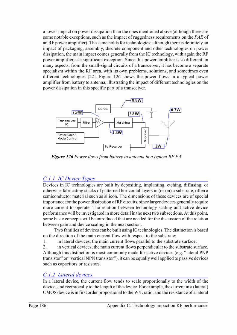
Page 186 Appendix C: Technology impact on RF performance
Figure 126 Power flows from battery to antenna in a typical RF PA
a lower impact on power dissipation than the ones mentioned above (although there aresome notable exceptions, such as the impact of ruggedness requirements on the PAE ofan RF power amplifier). The same holds for technologies: although there is definitely animpact of packaging, assembly, discrete component and other technologies on powerdissipation, the main impact comes generally from the IC technology, with again the RFpower amplifier as a significant exception. Since this power amplifier is so different, inmany aspects, from the small-signal circuits of a transceiver, it has become a separatespecialism within the RF area, with its own problems, solutions, and sometimes evendifferent technologies [22]. Figure 126 shows the power flows in a typical poweramplifier from battery to antenna, illustrating the impact of different technologies on thepower dissipation in this specific part of a transceiver.
C.1.1 IC Device TypesDevices in IC technologies are built by depositing, implanting, etching, diffusing, orotherwise fabricating stacks of patterned horizontal layers in (or on) a substrate, often asemiconductor material such as silicon. The dimensions of these devices are of specialimportance for the power dissipation of RF circuits, since larger devices generally requiremore current to operate. The relation between technology scaling and active deviceperformance will be investigated in more detail in the next two subsections. At this point,some basic concepts will be introduced that are needed for the discussion of the relationbetween gain and device scaling in the next section.
Two families of devices can be built using IC technologies. The distinction is basedon the direction of the main current flow with respect to the substrate:1. in lateral devices, the main current flows parallel to the substrate surface;2. in vertical devices, the main current flows perpendicular to the substrate surface.Although this distinction is most commonly made for active devices (e.g. “lateral PNPtransistor” or “vertical NPN transistor”), it can be equally well applied to passive devicessuch as capacitors or resistors.
C.1.2 Lateral devicesIn a lateral device, the current flow tends to scale proportionally to the width of thedevice, and reciprocally to the length of the device. For example, the current in a (lateral)CMOS device is in first order proportional to the W/L ratio, and the resistance of a lateral

Appendix C: Technology impact on RF performance Page 187
Figure 127 Simplified lateral device layout
(93)
resistor is in first order proportional to L/W ratio.
A simplified layout of a lateral device is shown in figure 127. For practical reasons, suchas the need to add contacts to a device, the actual device is often larger than the part ofthe device that carries the main current, and across which the main voltage drops occur.This can be approximated by adding compensation factors ()L and )W) to the length (L)and width (W), resulting in a total device size of ()L + L) by ()W + W).
A simple model for the current through a lateral device is based on the assumption thatthe current density J is proportional to the width/length (W/L) ratio when the voltageacross the device is kept constant. For passive and homogeneous devices, such asresistors, this is an accurate model, since such devices have a constant electrical fieldstrength:

Page 188 Appendix C: Technology impact on RF performance
(94)
(95)
(96)
For active devices, this model is less accurate, especially for short channels and indevices in which the substrate or a common well acts as a common terminal to all (partsof) active devices. However, it still is accurate to within ±15% for e.g. 0.5:m CMOSdevices when changing the gate width and length over one order of magnitude, as shownby the simulation results below:
The current I through a lateral device can therefore be modeled as:
1with " a device-dependent scaling constant. Parasitic effects of lateral devices can bemodeled as additional resistive and capacitive elements. The capacitive elements scalewith bottom area and perimeter length:
2 3with " and " device-dependent scaling constants. Please note that the parasitics aremostly caused by the total device area and perimeter, not just the part that carries themain current. The additional parasitic resistive elements end up as series elements thatscale with the length extensions:

Appendix C: Technology impact on RF performance Page 189
Figure 129 Simplified schematic for a lateral device with related parasiticelements
(97)
(98)
4with " a device-dependent constant. This results in the following simplified schematicfor a lateral device with its related parasitics:
cparThe parasitic will result in an additional, frequency-dependent current J that can beexpressed as:
The ratio between intended current and parasitic current can now be expressed as:
The partial derivative of this ratio with respect to the width W is:

Page 190 Appendix C: Technology impact on RF performance
(99)
(100)
(101)
(102)
cparwhich is positive definite for all W and L. Similarly, the partial derivative of the I/Iratio is:
which is negative definite for all W and L. This shows that, for any lateral device, theratio between intended current and parasitic current inevitably decreases with L andincreases with W. It also decreases at higher frequencies. Since the device current isproportional to W/L, any attempt to decrease the device current at higher frequencies byreducing device width and/or increasing device length will result in a relatively largerimpact of currents through the parasitic capacitance, bypassing the device.
Please note that this effect even occurs when )W and )L are zero. In that case,equation (6, 98, 101, 102, 102) simplifies to:
which has the same properties of the partial derivatives with respect to L and W. Thegain bandwidth product G BW can be derived by finding the frequency f at which the
cparI/I ratio reaches 2, that is, half the output current ends up in the parasitic capacitanceof the device, and therefore the gain is decreased by 3dB.

Appendix C: Technology impact on RF performance Page 191
Figure 130 Simplified layout of a vertical device
(103)
(104)
C.1.3 Vertical devicesIn a vertical device, the current is in first order proportional to both the length L and thewidth W of the device when the voltage across the device is kept constant. For example:in a vertical NPN transistor, the current is proportional to the L*W product, and in aparallel-plate capacitor the capacitance (and therefore the current by constant voltage) isproportional to the L*W product as well.
A simplified layout of a vertical device is shown in figure 130. Like lateral devices,most vertical devices need additional space for contacts, spacing between patterns, etc.,which results in additional width and length ()L and )W). Added to the intrinsic device,this results in a total device size of ()L + L) by ()W + W), as shown in figure 130.
In vertical devices, both passive and active, the current scales accurately with W*L. Thisis due to the fact that the electrical field distribution in such devices is almostindependent of the scaling, since it is orthogonal to both scaling dimensions. As withlateral devices, expressions for the scaling of intended and parasitic currents can bederived. The scaling of the intended current is modeled as:
Again, the parasitic capacitance of a vertical device scales with bottom area and perimeterlength:

Page 192 Appendix C: Technology impact on RF performance
(105)
(106)
(107)
(108)
The current caused by the parasitic capacitance is:
This results in a ratio of intended and parasitic current of:
From this, the partial derivatives for L and W respectively, are derived as follows:
With both partial derivatives being definite positive, the ratio between intended andparasitic current will be smaller (and thus worse) for smaller values of either L or W. Inother words: any vertical device will unavoidably show a worse ratio between intendedand parasitic current for smaller values of W and L, that is, for smaller intended currents.Also, the ratio decreases at higher frequencies. In a similar way, it can be shown that thesame conclusion holds even if )L and )W are zero.
The gain bandwidth product G BW can be derived in the same way as for lateraldevices:

Appendix C: Technology impact on RF performance Page 193
(109)
Since in IC processes, devices are built either as lateral or vertical devices, and since forboth types of devices the ratio between intended and parasitic current becomes smaller(and thus worse) for smaller currents through the device and for higher frequencies, thereis a fundamental problem with scaling devices in any IC technology to achieve low powerat high frequencies. These problems can be reduced by special technologies, such asvertical scaling, trenches, SOI, and SOA, but the fundamental problem remains.
C.2 Other technology-induced performance limitations
In addition to the scaling of devices, there are other performance limitations that arerelated to, but not directly part of, IC technology. The two most relevant ones arediscussed below.
C.2.1 Modeling problemsOne complicating factor in developing RF front-end circuits, and especially when lowpower is an important design target, is the accurate modeling of the circuit. As discussedin the previous section, the impact of device extensions )W and )L, and of parasiticsrelated to the perimeter of devices, increases with decreasing device sizes and currents.Therefore, low-power circuits operate closer to the high-frequency limits of an IC processthan circuits with higher currents at the same frequency. In other words, the designmargin between requirements and process performance is smaller for low-power RFcircuits. In addition, the impact of additional parasitics, such as perimeter capacitance,becomes more important.
Accurate modeling of all devices, but also of interconnect, substrate, packagingetc., is required in order to achieve a low-power RF front-end design within a reasonableamount of time. For some devices, very accurate models are available, for example forbipolar transistors. Models such as Mextram [36] provide sufficient accuracy for mostcircuits. As a result, bipolar transistor model inaccuracies no longer contributesignificantly to overall simulation inaccuracies. For other effects, only very limitedmodels are available, for example for substrate electrical coupling in IC processes thatuse intermediate substrate impedances (around 10Scm).
It is not likely that accurate models for all relevant effects will be available in thenear future. And even if they would be available, along with the appropriate parameters

Page 194 Appendix C: Technology impact on RF performance
for each of the models and for the relevant IC process, the number of potentiallyrelevant effects is so high, that it would be impractical to simulate circuits with modelsfor each of these effects. The simulation time would be prohibitive, even with thecomputer capacity increases that can be expected over the next five years. Moreover,many of these models require information that is simply not available in the circuit-design phase of a top-down design approach. For example, wire lengths and shapes,interconnect levels, relative positions of components and circuits on the IC substrate, etc.will not be known until the layout phase is (partially) completed, and layout parameterextraction and back-annotation are carried out.
In practice, designers make choices - often based on experience - about what tomodel, and use estimates for parameters that are not exactly known at this stage in thedesign process. This is where experienced designers distinguish themselves from lessexperienced designers: making the right choices for the effects that need to be modeled,and the right estimates for unknown parameters, has a very big impact on theperformance of the IC, and determines to a high degree the number of redesigns neededto arrive at the required level of performance.
The small margin between required and achievable performance, and as aconsequence the large number of effects that need to be taken into account, are the maindrivers for improved modeling. One way to reduce or even avoid this problem is to usetechnologies that have a much higher performance than is required for a specificapplication. This is of course not very cost efficient, and therefore not always possible.
Another way to reduce the modeling problem is to integrate the circuit-design andlayout phases in the design process. This is already done for very high frequency circuits,but is limited to circuits of low complexity. Making changes in a layout is often muchmore time consuming than making the same changes in a schematic representation of thecircuit. For example, changing a resistor or capacitor value can have dramaticconsequences in a layout, requiring major changes to the position of many other devicesand their interconnect, whereas at the schematic level, only a single number changes inthe schematic. For larger circuits and bigger changes, the amount of work can cause longdelays in the development project.
A third way to reduce the modeling problem is to build circuits from larger buildingblocks that have been previously designed and characterized, similar to the design ofdigital circuits using building blocks at higher abstraction levels, such as gates, registers,memories, and cores. However, this does not solve all modeling problems, since therecan also be significant unintended interactions between blocks.
C.2.2 Inter-block interactionUnintended, or parasitic, interaction between circuit blocks can be caused by severaleffects, including:C Non-linear input and output impedancesC Thermal and/or electrical coupling through the substrateC Magnetic coupling of internal inductors in each of the blocksC Magnetic coupling of internal inductors with bond wiresC Injection of spurious signals that are present at inputs and/or outputsC Coupling through power supply and ground lines
Modeling and characterizing all these effects is cumbersome at best, and almostimpossible in those cases where the relative positions of the circuit blocks involved, and

Appendix C: Technology impact on RF performance Page 195
of other circuit blocks, play a significant role. This situation can be improved bydesigning circuit blocks in such a way that they are relatively insensitive to most of theseeffects, and that they cause as little thermal, electrical, and magnetic disturbance aspossible. This is of course not always possible because of the limited margins betweenavailable and required performance, and because of cost.
One technology that helps to reduce inter-block interaction, and at the same timealleviates modeling problems, is RF-module technology. Using this technology, circuitblocks can be implemented on individual physical ICs, and packaged and connected inan RF module. By modeling and characterizing the building blocks based onmeasurements of the physical ICs, their behavior can be accurately predicted. Theinteraction between circuit blocks is minimized by the larger physical distance in amodule, the elimination of a common semiconductor substrate, and decoupling of thepower and ground signals between the blocks.

Page 196 Appendix C: Technology impact on RF performance

Appendix D: Current design methods & results Page 197
Appendix
DCurrent design methods & results
In the following sections, short descriptions of the different categories of design methodsare presented.
D.1 Automatic versus manual design methods
Automatic design methods are based on tools that automatically carry out the stepsprescribed in the design method. From a methodology point of view, there is littledifference between automatic and manual design methods: automatic design methods canalways be carried out manually, but this might in some cases not be practical because ofthe amount of work involved. Conversely, manual design methods can often beimplemented in an automatic way, although this is less obvious. Especially designmethods based on pattern recognition and experience are difficult to automate.
An example of an automatic design method is circuit sizing using the tool Adapt[65]. This design method covers part of the schematic design abstraction level, in whichthe circuit topology, implementation technology, and target specifications have alreadybeen defined. Using this method, the parameter values of the various devices can beoptimized according to a specified optimization criterion.
An example of a manual design method will be discussed in the next chapter.

Page 198 Appendix D: Current design methods & results
D.2 Iterative versus single-shot methods
Iterative design methods contain a loop in their design process. At the beginning of aniteration through this loop, a version of the design is available that does not meet allperformance requirements. In the loop, some operations are carried out on this design thatmodify its performance. At the end of the loop, the performance is compared to theperformance requirements. If the requirements are not met, the design is used as a startingpoint for the next iteration through the loop. Iterative circuit design methods, in whichthe evaluation of the achieved performance is determined through a circuit simulator, arealso called “simulation-based methods” [66, 66, 66]. Many, and maybe even most,current RF products are designed based on iterative methods as described in Section 1.4.
Single-shot design methods achieve their results without the need for iterations.These design methods are often based on equations or rules, and are often associated withproperties such as “correct by construction” and “first time right”. Single-shot methodshave become popular in the digital area, but are currently also being proposed and usedfor RF design.
As with all design methods, it is important to realize that results achieved throughsingle-shot design methods are only as valid and accurate as the models and assumptionson which such methods are based. Therefore, methods such as single-shot, exact, andalgorithmic are not necessarily better than heuristic, iterative, and approximate designmethods. An approximate solution based on accurate models can be much more usefulthan an exact solution based on unrealistic models. This also explains the differences inpopular design methods between digital and RF design. In digital design, the modelsmore accurately predict the performance of a design, making single-shot methods morelikely to be successful than in the RF area.
D.3 Algorithmic versus heuristic methods
Heuristic methods are based on practical and empirical rules rather than theory orscientific principles. This category includes expert systems, but also the manual designmethods employed by many experienced designers. The main disadvantage of heuristicmethods is that it cannot be guaranteed that an achieved solution is optimal, or evenfunctional. However, this method often results in solutions that would be very difficultor impossible to achieve otherwise, especially for very complex design problems.

Appendix D: Current design methods & results Page 199
D.4 Model versus reality based methods
Most current RF IC design methods use models of the system, circuit, and componentsthat are used in the design. This has several advantages:C Models allow access to all signals, parameters, and internal states of the components,
circuits and system, without disturbing the operation of the model. This can be anenormous help in understanding the behavior of a component, circuit or system.
C Models do not break, and give 100% reproducible results.C Models can be used for designs at a time that the actual components, circuits, or
systems are not yet available, or cannot yet be fabricated.There are also disadvantages to the use of models. Especially the accuracy of the modelis usually limited, either because the model does not accurately describe the behavior ofsome effects, or because some effects are not included in the model at all.
As an alternative, a design method can directly use the components, circuits andsystem that will be part of the final design. An example of this approach is the traditionaliterative “trial and error” method of RF design by soldering components on a PCB,carrying out measurements, and adjusting the design until the required performance isachieved. The outcome of such a design method is simultaneously the design and thefinal implementation of this design.
Sometimes it is not obvious which method is being followed. For example, aprototype of a volume product could be developed using a reality based method.However, a prototype that meets all requirements does not guarantee a design that meetsall requirements: because of parameter spread in volume production, a significantpercentage of products could still fail to meet the requirements. Therefore, a prototypehas to be considered a model in the context of design methods.
D.5 Exact versus approximate methods
An exact design method results in a design that exactly meets the requirements, andtherefore is the optimum design for the given target specifications. An approximatedesign method results in a design that approximately meets the requirements, andtherefore is close to the optimum design for the given target specifications. Approximatemethods are popular, because the limited accuracy of the models, and assumptions usedin RF design methods, reduce the relevance of an exact solution.
Whether an exact method is more appropriate than an approximate one dependsalso on the application for which a design is being developed. In some applications, thereare no hard requirements on performance, although performance of course plays animportant role in the value of a design. In other applications, hard performancerequirements do exist, for example as type approval requirements that need to be metbefore any product can be sold.

Page 200 Appendix D: Current design methods & results
D.6 Explicit and implicit design methods
In explicit design methods, the goal of the design and the method to be used are formallydescribed. In implicit methods, the design method or the requirements are not explicitlystated. Also in this case, the method being used might not be obvious. Even if a completeformal specification and design method is available, several aspects might not beformally specified but are still very much expected. For example, the specifications fora low noise amplifier usually provide gain, noise figure, linearity, power dissipation,input and output impedance, power supply voltage and temperature range. Often, they donot explicitly include the requirement to:C not oscillateC not generate significant spurious signals on the power supplyC not explodeC have limited switch-on currentsetc. Still, if one of these requirements would not be met, the customers for such a designwould probably not be satisfied by the result. In practice, it is very difficult or evenimpossible to provide a complete, formal, specification for anything but the most trivialproduct.
D.7 Bottom-up versus top-down design methods
In bottom-up design methods, the design starts with the investigation of the possibilitiesand performance of the individual parts of a design, and subsequently these parts arecombined into a complete design that meets the specifications. Top-down starts from thespecifications for the complete design, and derives from these the architecture andspecifications for subcircuits, from which in turn topologies and subcircuit parametersare derived [13].
Both design methods have disadvantages:C by starting from individual parts of a design, a global optimization of e.g. gain, noise
and linearity distribution is difficult to achieve. C by starting from the specifications, assumptions have to be made about the feasibility
of subcircuit performance that can only be verified in a later stage of the designprocess.
For that reason, several meet-in-the-middle approaches have been defined, such asbottom-to-top creation [8], that combine partial top-down with partial bottom-upmethods.

Appendix D: Current design methods & results Page 201
D.8 Custom versus reuse design methods
One way to speed up the design process is by reusing parts of a circuit that has beendesigned previously. Reuse can occur at any abstraction level of the design, such assystem, schematic, and layout. The main disadvantage of a reuse method is that it onlyis practical if a circuit or part of a circuit with acceptable specification and implementedin an appropriate technology is available. This is often not the case. Custom design fromscratch is one way to solve this, but in some cases it can be more efficient to design acircuit by modifying an existing circuit, to convert it to another technology, or to modifyits performance. Modifying circuits for reuse is called recycling. An example of recyclingis the widespread use of double-balanced mixers based on the Gilbert cell. Even thoughall such mixers use the same circuit topology, they can have widely varying performancedepending on bias conditions, device sizes, resistor values etc. Also, they can beimplemented in many different technologies.
D.9 Abstraction levels covered by design methods
Finally, different design methods address different abstraction levels of a design process.In the context of this thesis, we will concentrate on system, schematic, and layout levels.Design methods often only cover one or two of these abstraction levels, requiringadditional design methods to cover the other levels, and yet another design method forusing the combination of two or more design methods.

Page 202 Appendix D: Current design methods & results

Appendix E: Limiting in zero-IF receivers Page 203
Appendix
ELimiting in zero-IF receivers
In a superhet receiver for frequency modulated systems (fig. 131, 133, 133), it is possibleto realize the IF gain by limiters without significantly affecting the demodulationaccuracy. This can easily be seen from a square-wave baseband signal "data(t)",representing a digital data sequence "0101010101" (Fig. 132).

Page 204 Appendix E: Limiting in zero-IF receivers
Figure 131 Superhet architecture
Figure 132 Digital baseband signal
If this baseband signal is applied to the input of a frequency shift keying (FSK)
c *modulator, which has a center frequency f and a swing f , this will result in an IF signalwith the following phase N(t) versus time (fig. 133).

Appendix E: Limiting in zero-IF receivers Page 205
Figure 133 Phase of the IF signal as a function of time
(110)
Figure 134 Instantaneous signal value of the IF signal as afunction of time
With N(t) equal to:
A more conventional representation of the IF signal is obtained by plotting theinstantaneous signal value I(t) rather than the phase value against time, as shown in fig.134. The information in the two representations, however, is the same and the structuresthat will be discussed in this text are simpler to understand with reference to the phasecurve rather than the instantaneous signal value curve of the IF signals.

Page 206 Appendix E: Limiting in zero-IF receivers
(111)
Figure 135 Instantaneous value of the IF signal afterlimiting
Figure 136 Phase of the IF signal after limiting.
With I(t) equal to:
After limiting this IF signal, a signal LI(t) is obtained as shown in fig. 135.
Due to the lack of amplitude information, the phase of this signal is often determined onthe basis of the last zero crossing (as is the case, for example, in a count detector or pulsecount demodulator). The reconstructed phase variation ImpRec(t) is shown in fig. 136,again plotted as a function of time.
The value of the function ImpRec equals B times the number of zero crossings of the

Appendix E: Limiting in zero-IF receivers Page 207
Figure 137 Original and reconstructed phase of the IFsignal
instantaneous IF signal after limiting, in the interval [0,t). Reconstruction by othermethods, in which more information than only the last zero crossing is used (for example,PLL demodulators), will result in a different (and sometimes more accurate) phase
variation. A pulse counter demodulator is relatively simple to implement, and thereconstructed phase rather accurately approaches the original phase, as long as the IFfrequency and modulation index are both high. The output of this type of demodulatoris shown in fig. 137:
The error introduced after demodulation can be modeled in the same way as quantizationnoise in an A/D converter, because the operation in the phase domain corresponds toquantizing the phase. A major difference is that the phase is a cyclic phenomenon, so thatthe "range" of the phase quantizer is not limited, unlike A/D converters for voltages orcurrents. This property makes it possible to enlarge the apparent range per period of thebaseband signal by increasing the carrier frequency. This corresponds to adding a linearlyincreasing voltage to the input signal of an A/D converter, and is similar to the effect ofdithering in such a converter: in either case the number of transitions is enhanced whilethe input signal remains the same, so that the input signal can be approximated moreaccurately.
The quantization effect increases when reducing the IF frequency. Therefore it alsobecomes more obvious in the phase domain (fig. 138).

Page 208 Appendix E: Limiting in zero-IF receivers
Figure 138 Phase of an IF signal at a lower IF frequency
Figure 139 Instantaneous value of the IF signal at a lowerIF frequency
The instantaneous value of the IF signal is shown in fig. 139:
After limiting, this signal is transformed into (fig. 140):

Appendix E: Limiting in zero-IF receivers Page 209
Figure 140 Instantaneous value of the IF signal with alower IF frequency after limiting
Figure 141 Reconstructed phase of the limited IF signal ata lower IF frequency
The reconstructed phase of the limited IF signal now becomes (fig. 141):
By comparing the reconstructed phase to the original phase, it is obvious that thedifferences have increased compared to the differences at a higher IF frequency (fig.142):

Page 210 Appendix E: Limiting in zero-IF receivers
Figure 142 Reconstructed and original phase of the IFsignal at low-IF frequency

Appendix E: Limiting in zero-IF receivers Page 211
Figure 143 Phase variation of the IF signal in a zero-IFreceiver
Figure 144 Instantaneous signal value of the IF signal in azero-IF receiver
This increased difference corresponds to the increased quantization noise. Since the phasechange in one bit period has decreased at a lower IF frequency, the resolution of thequantizer, in terms of “least significant bit transitions”, has decreased proportionally.
E.1 Problems with limiting in zero-IF receivers
In a zero-IF receiver, the quantization error becomes very big since the IF frequency iszero. The only zero crossings are caused by the frequency deviation. If the frequencydeviation is small compared to the bit frequency, this can result in extreme quantizationerrors in the phase domain. Fig. 143 shows the phase variation of the IF signal in a zero-IF receiver, using the same data signal and frequency deviation as in the previous section:
The instantaneous IF signal value for this situation is shown in fig. 144:

Page 212 Appendix E: Limiting in zero-IF receivers
Figure 145 Instantaneous value of the IF signal afterlimiting in a zero-IF receiver
Figure 146 Reconstructed phase of the limited IF signal ina zero-IF receiver
The result after limiting is shown in fig. 145:
Since it is impossible to distinguish positive and negative frequencies on the basis of thissingle IF signal, phase reconstruction is very limited (fig. 146):
When comparing this reconstructed phase with the original phase, the differences are veryobvious (fig. 147):

Appendix E: Limiting in zero-IF receivers Page 213
Figure 147 Reconstructed and original phase of the limitedIF signal in a zero-IF receiver
Figure 148 Phase variation of the I and Q signals in azero-IF receiver
In a zero-IF receiver, at least to IF signals are necessary to distinguish between positiveand negative IF frequencies. These signals are usually referred to as I and Q. The phasevariation of these signals is represented in Fig. 148:
The associated instantaneous signal values are represented in fig. 149:

Page 214 Appendix E: Limiting in zero-IF receivers
Figure 149 Instantaneous values of the I and Q IF signalsin a zero-IF receiver
Figure 150 I and Q signals after limiting
When sending these signals through a limiter, the following results will be obtained (fig.150):
The combination of the I and Q signs indicates in which quadrant the phase is at thatmoment. Since there is assumed that the phase variation is a continuous function of time,the phase variation may be reconstructed from the successive quadrants, except for oneconstant value (the initial phase). The frequency of the IF signal can now also bedetermined, both for positive and negative frequencies. The reconstruction of the phasevariation established in this manner shows the following pattern (fig. 151):

Appendix E: Limiting in zero-IF receivers Page 215
Figure 151 Reconstructed phase of the I and Q signals
Figure 152 Reconstructed and original phase of the I andQ signals
This phase variation follows the IF phase more accurately than the reconstruction basedupon a single IF signal (Fig. 22), but it is still very limited (Fig. 152):
The previous examples have been based on a modulation index of 0.3. When reducingthe modulation index to less than 0.25, no reconstruction of the limited signal will bepossible any more (fig. 153).

Page 216 Appendix E: Limiting in zero-IF receivers
Figure 153 Reconstructed and original phase of a limitedIF signal with a modulation index of 0.2

Appendix E: Limiting in zero-IF receivers Page 217
Figure 154 Multi-branch receiver
This demonstrates the problem of reconstructing the phase variation in FSK-modulated systems with a low modulation index, when using a zero IF architecture thathas limiters in the IF signal path.
E.2 Existing solutions
There are at least two different approaches to solving this problem: C the quantization of the phase can be carried out using a smaller phase difference
between quantization levels;C the reconstruction of the signal in between two quantization levels can be carried out
more accurately.
Reducing the step size can be achieved by using additional IF signals [94] (fig. 154).
In a multi-branch receiver, the VCO needs to generate multiple (in this example 4) localoscillator signals (in this case with phases N1, N2, N3 and N4). Each LO signal isconnected to a different mixer, and the output of these mixers provide the multiple IFsignals (in this case "IF1" through "IF4"). This architecture is rarely used, however, sincethe complexity of the receiver increases significantly: each additional IF signal calls fora new mixer, a new filter, and an additional VCO output.
Accurate reconstruction in between quantization levels is achieved, for instance,by PLL demodulators. The use of such a demodulator in a zero-IF receiver, however,requires an oscillator that can generate both positive and negative frequencies. Thisimplies that such an oscillator needs to cover an infinite number of octaves of tuningrange. This is difficult to realize with practical boundary conditions.

Page 218 Appendix E: Limiting in zero-IF receivers
(112)
(113)
E.3 New solutions
Both approaches to solve the limited zero-IF receiver problem have drawbacks: highcircuit complexity for the multi-branch receiver, and a difficult VCO for the PLLdemodulator. In this section, new solutions that avoid these drawbacks will beintroduced. Finally, an implementation that combines both new solutions will bepresented.
E.3.1 Low-complexity generation of multiple IF signalsThe multiple IF signals in a multi-branch receiver are not independent. Two IF signalswith different phase are can be converted into an orthogonal pair by linear transformation.In fact, most two-branch receivers already use such an orthogonal pair. Other IF signalscan then be constructed from these IF signals by forming linear, weighted, combinationsof the orthogonal pair.
Let IF(") represent the IF signal with phase ". The orthogonal pair of IF signals Iand Q now correspond to:
Any new IF signal with phase $ can now be generated by a linear combination of I andQ:
Therefore the creation of additional IF signals can be postponed to a later stage in thesignal processing chain. This reduces the increase in circuit complexity, since additionalsignal processing stages only need to be implemented from the point where the additionalIF signals are created. Postponing this to the last possible stage result in theimplementation with the lowest complexity.
The last possible stage at which the linear combination of I and Q, as described in(113), can be carried out, is the stage before the first non-linear processing of the IFsignal, i.e., before the limiters. The linear combination from (113) can be accomplishedthrough a simple resistive interpolation network, similar to the interpolation circuits usedin an folding & interpolation ADC [95]. A block diagram of a receiver using thisinterpolation approach is shown in fig. 155.

Appendix E: Limiting in zero-IF receivers Page 219
Figure 155 Block diagram of a zero-IF interpolation receiver
In a zero-IF interpolation receiver, the additional VCO phase generators, mixers andfilters can be replaced by a small number of resistors and an inverter. The inverter in abalanced system can be replaced by a crossing of the signal wires. Further resistors canbe added between the resistor network and the inputs of the limiters in order to maintainthe same signal amplitude and source impedance, and therefore the same phase shift athigh frequencies. This is comparable to the delay compensation in interpolation networksof folding A/D converters [95].
An interpolation zero-IF receiver can achieve a arbitrarily small error whendemodulating frequency modulated signals by increasing the number of IF signals. Sinceeach halving of the quantization step calls for a doubling of the number of limiters andresistors in the interpolation network, this approach is limited both because of theexponentially increasing cost and because of the exponentially increasing accuracyrequirements of these elements. Therefore, a reconstruction method to complement theinterpolation approach would be very useful.
E.3.2 Accurate reconstruction in superhet receiversThe reconstruction method used in the previous examples is a hold function of the lastknown phase value. Although this is an obvious and easy to implement method, it isknown from sampling theory that better reconstruction possibilities exist for equidistantlysampled signals.
The continuous-time phase quantization process may also be considered a samplingprocess. In a quantization process a signal is described as a function of time while onlythe interval in which the signal occurs is known at any instant. This usually results in astatistical description of the signal and its quantization error. In fact, the quantizationerror is often modeled as a noise source in quantization process models.
A continuous-time quantization process may also be considered as a samplingprocess, because there are instants in time at which the value of the signal is exactlyknown, i.e. at the moment that a transition between two quantization levels occurs (fig.156).

Page 220 Appendix E: Limiting in zero-IF receivers
Figure 156 Sampled value of an IF signal with a lowfrequency
Figure 157 Sampled and original values of the lowfrequency IF signal
When comparing this signal with the original signal (fig. 157), it is obvious that thesamples represent the exact value, without any quantization error.
Since traditional sampling theory is based on equidistant samples, and requires Nyquistbandwidth limits for reconstruction, it does not apply directly to the sampling as shownin fig. 157. The sampling is obviously non-equidistant, and the bandwidth of the phasetrajectory is seldom, if ever, specified or controlled in telecommunication transceiversystems.
In a superhet architecture, this can be solved by considering the inverse functionof the IF signal, namely, the time as function of the phase of the signal. This is possiblebecause the IF frequency is significantly higher than the frequency deviation, making thephase trajectory as a function of time strictly monotonic. Hence, an inverse function isguaranteed to exist. Fig. 158 shows a curve of time plotted against phase for the samesignal:

Appendix E: Limiting in zero-IF receivers Page 221
Figure 158 Time as a function of IF signalphase
Figure 159 Quantized IF signal plotted astime samples versus phase
Fig. 159 shows that the quantized version of this IF signal can be interpreted as anequidistantly sampled signal:
If the time as a function of phase is band-limited, a simple and perfect reconstructionbased upon the standard sampling theory is possible. This does call for a sufficiently highsampling rate with respect to the bandwidth of the time function, but this requirement canalways be satisfied by making the sampling period (thus the distance in the phase domainbetween two quantization steps) sufficiently small. Even if, as will be often the case, asystem does not guarantee that the time as function of phase is bandlimited, the errorsintroduced by aliasing might still be smaller than those introduced by a simple holdfunction.

Page 222 Appendix E: Limiting in zero-IF receivers
Figure 160 Accurate reconstruction of the baseband signal
This method cannot be applied to receivers in which the phase variation as afunction of time can not be inverted, i.e. if this function is not strictly monotonic.Therefore, low-IF receivers and superhet receivers can use this method, but zero-IFreceivers cannot.
E.3.3 Accurate reconstruction in zero-IF receiversIn the special case of binary FSK modulation, a solution exists in which the phasefunction need not be inverted. This solution uses the symmetry of the phase functionaround a transition of the baseband signal. When the phase quantization levels are closeenough, the transition of the baseband signal is halfway between the nearest transitionsof the phase signal through the phase quantization levels. This is shown in fig. 160.
The top curve of fig. 160 shows the baseband signal, i.e. the data to be transmitted. In thisexample, a random data sequence "101100100101" is used. The associated phasevariation of the IF signal in a zero-IF receiver is shown in the second curve ("N"). Thehorizontal dashed lines represent the quantization levels, with a quantization step of B/2.This IF signal is then converted into time samples as a function of phase using adifferentiate-and-cross-multiply (DACM) demodulator, as shown in fig. 161.

Appendix E: Limiting in zero-IF receivers Page 223
Figure 161 Diagram of a DACM demodulator for zero-IF receivers
(114)
(115)
This DACM demodulator produces positive pulses at a positive transition of the phaseof the IF signal through a phase quantization level, and a negative pulse at a negativetransition. These pulses are shown in the third curve ("Dem") of fig. 160. A simple, butinaccurate reconstruction can be obtained by integrating the pulses, or by holding the signof the last pulse, as is shown in the fourth graph ("Imp.Rec") of fig. 160.
A perfectly accurate reconstruction (“Perf. Rec.” in fig. 160) can be obtained bydelaying the transitions of the demodulator output to the moment halfway between twosuccessive pulses with opposite signs (“Time Avg” in fig. 160). This method requiresthat sufficient pulses per data symbol are obtained, so that any possible bit sequence canbe decoded. This limits the quantization step size. In addition, a fixed time delay needsto be incorporated in the reconstruction circuit, to guarantee causality. This delay is atleast half the maximum time between two opposite pulses.
The following variables will be used for a more precise formulation of theseconditions:T: symbol period
dT : fixed delay in the reconstruction algorithm R: symbol rateX: maximum phase excursion in time TM(t): phase at instant t
IFf : frequency of the IF signal n: number of phase quantization levels as a result of which the quantization distance
is B/n.
The following relations exist between these variables:
and:

Page 224 Appendix E: Limiting in zero-IF receivers
(116)
(117)
A perfect reconstruction can be achieved the following condition is satisfied:
using the following algorithm: 1. Look for the first pulse in the "Dem" signal;2. Set the reconstructed data to a value that corresponds to the sign of the pulse; 3. Repeat the next 3 steps until the end of the signal;4. If a positive pulse is followed by a negative pulse, set the reconstructed data to
d"0" at an instant that corresponds to the fixed delay T plus the average of theinstants of the positive pulse and the negative pulse;
5. If a negative pulse is followed by a positive pulse, set the reconstructed data to
d"1" at an instant that corresponds to the fixed delay T plus the average of theinstants of the positive pulse and the negative pulse;
6. If the period of time between two pulses exceeds 2T, change the value of thesignal every period of time T after the symbol that follows the symbol in whichthe last pulse occurred, and before there is another period of time T in which apulse occurs.
The major disadvantage of this algorithm and the corresponding boundary conditions isthat the period of time between two successive opposite pulses may be arbitrarily long.
dAs a consequence, T needs to be infinitely large as well, so that the memory capacityfor the implementation will also have to be infinitely large.
This may be avoided if more information about the signal is known, for example, that itwill be partitioned in packets of predefined maximum length, and/or that the symbolsequence "10101010101010 ..." has a predefined maximum length. There are modulationsystems in which this can be guaranteed, for example, (d,k,N)-constrained sequences (d$ 1) for super density CD, and the PHY and MAC layers for the DECT protocol.
If no further information about the signal is known, a practical implementation of thisalgorithm can still be obtained by using a stronger boundary condition for thequantization level:
With this stricter boundary condition, the maximum period of time between two pulsesis 2T, so that the minimum delay in the reconstruction becomes T. This means that amemory with a capacity of only one symbol is sufficient, and that step 6 from thealgorithm may be omitted.

Appendix E: Limiting in zero-IF receivers Page 225
Figure 162 Extended DACM demodulator for interpolation receiver
The smaller quantization step can be obtained by using a multi-branch receiver. This doesrequire an extension of the DACM demodulator, as shown in fig. 162:

Page 226 Appendix E: Limiting in zero-IF receivers

Appendix F: Solution of the general problem Page 227
Appendix
FSolution of the general problem
The mathematical formulation of the general problem of the optimum distribution ofgain, linearity and noise distribution for an arbitrary number of cascaded stages, asformulated in this thesis, was solved by dr. ir. A.J.E.M. (Guido) Janssen at the PhilipsResearch Laboratories, Eindhoven. He reformulated the problem in a different way usingthe following definitions:

Page 228 Appendix F: Solution of the general problem
(118)
(119)
(120)
(121)
and, by convention:
i iNote that x can be interpreted as the output IP3 of block i, whereas y can be interpretedas the partial gain of blocks 1 through i.
Also, let
Note that a can be interpreted as the part of the noise factor that exceeds the noise factorof an ideal circuit block (F=1).
i iThen the x , y are positive but otherwise unrestricted by the definitions in equation (118).Also:
The problem now takes the following form:
Given

Appendix F: Solution of the general problem Page 229
(122)
(123)
(124)
(125)
find the minimum of:
under the conditions that:
Condition (124) is the equivalent of Friis formula, whereas condition (125) is the
tot iequivalent of the IP3 spec of a front end. Please note that at this point, y is a function
i iof x , b, a and a.
This problem was solved as follows:
0 1 n-1 nTake y , y , ... , y , y > 0 such that the constraints (124) and (125) are satisfied. Then
1 n determine the minimum of P in (123) as a function of x , ... , x under the constraint (125).
0 1 n-1 n 0 1This yields a minimum value P(y = (y , y , ... , y , y )). Now determine y = (y , y , ... ,
n-1 ny , y ) such that the constraints (124) are satisfied while P(y) is minimal.
Thus there are two steps:
Step 1:
0 1 n-1 n iGiven y , y , ... , y , y > 0 such that (125) holds, minimize (i.e. find x ):

Page 230 Appendix F: Solution of the general problem
(126)
(127)
(128)
(129)
(130)
iwhich yields a minimum value P(y) and x (y).
Step 2:Minimize P(y) under the condition that (124) holds.
Details of step 1:
0 1 n-1 nFix y , y , ... , y , y > 0 Based on Lagrange’s multiplier rule [40], there is a point where the extrema of P occurunder the constraint that there is a multiplier 8 such that:
iThe extrema represent the minimum power for OIP3 while meeting the IP3 specs.This gives:
The constraint in (126) needs to be satisfied, hence 8 needs to be determined such that:
The first part of this equation ensures that the IP3 spec is met, while the second part
irepresents the solution of x for minimum power.
Evidently -8 > 0. This yields
iThis can be used to express 8 as a function of y , resulting in a new function for x:

Appendix F: Solution of the general problem Page 231
(131)
(133)
(134)
(136)
i ix = f(y , k , b).
At the extremum point this evaluates to:
In this expression, the value for that follows from (130) was substituted.
Details of step 2:It is also valid to minimize:
iwhere the z > 0 are constrained by the equivalent of Friis formula, see (124):
The constraints are dealt with as follows:

Page 232 Appendix F: Solution of the general problem
(137)
(138)
(139)
(140)
(141)
nwhich takes out z , and
0which takes out z .
Thus Q(z) in (136) must be minimized under the constraint (137). By again applyingLagrange’s multiplier rule, there has to be a multiplier : at the minimum point such that:
This gives:
The constraint (137) needs to be satisfied, hence : should be determined such that:
This gives:
Then, at the minimum point, Q has the value:

Appendix F: Solution of the general problem Page 233
(142)
(143)
(144)
(145)
(146)
Therefore, the minimum value of P equals, see (131):
and is reached for, see (133):
and, see (129):
where, see (130):

Page 234 Appendix F: Solution of the general problem
(147)
iThus, using (141), x simplifies to:

Appendix G: FAT transforms Page 235
Appendix
GFAT transforms
Many of the specification parameters of a transceiver correspond one-to-one to thesystem specification. Table 14 shows a list of such parameters.
Field Description Unit Fmt
RxMinFreq Minimum receive frequency MHz N
RxMaxFreq Maximum receive frequency MHz N
TxMinFreq Minimum transmit frequency MHz N
TxMaxFreq Maximum transmit frequency MHz N
RXChannelPitch Grid of the RX channel raster kHz N
RXChannelBW 3dB bandwidth of one RX radio channel kHz N
TXChannelPitch Grid of the TX channel raster kHz N
TXChannelBW 3dB bandwidth of one TX radio channel kHz N
BasebandBW 3dB bandwidth of one baseband channel kHz N
NrOfChannels Number of receive/transmit channel pairs I
RXFreqError Maximum error in RX RF frequency kHz N
RXModulation Description of RX modulation type A60
RXDeviation Frequency deviation of RX FM type signals kHz N
TXFreqError Maximum error in TX RF frequency kHz N
TXModulation Description of TX modulation type A60
TXDeviation Frequency deviation of TX FM type signals kHz N
TXMinSignal Minimum transmit power level W N
TXMaxSignal Maximum transmit power level W N
TxAvgSignal Average transmit power level W N
TXStepSignal Transmit power level step size dB N

Field Description Unit Fmt
Page 236 Appendix G: FAT transforms
RXMinRssi Minimum RSSI indication required dBm N
RXMaxRssi Maximum RSSI indication required dBm N
RxStepRssi Maximum step size of RSSI dB N
DataRate Raw data rate across the radio channel kbps N
TimeSlot Duration of a single timeslot ms N
Transceiver specification parameters that are identical to system spec parameters
Other receiver specifications are derived from the system specification through formulas.In these formulas, the field names of the database table are used as variables to indicatethe appropriate values from the database tables. The table from which these databasefields are taken is indicated as a subscript. The following parameters are derived (table14).
Field Description Unit Fmt
RxNF Receiver Noise Figure dB N
Cochannel Cochannel suppression dB N
Rx1dBCompr Receiver 1dB compression point dBm N
RxAgcRange Receiver optimum AGC range dB N
RxDutyCycleAct Rx Percentage “on” time in active mode % N
TxDutyCycleAct Tx Percentage “on” time in active mode % N
Transceiver parameters derived from system parameters
Also, the following parameters are derived from detail tables of the System.db table, andtranslated to detail tables of the Trx.db table, to show offset-frequency dependence (table14).
Parameter Description Detail Table
Selectivity Selectivity TrxSel.db
IP3 Receiver IP3 spec TrxIP3.db
RxVcoNoise Receiver VCO phase noise RxVCO.db
Transceiver parameters derived from other system tables
The noise figure is derived from the thermal noise floor in the channel bandwidth, theminimum signal power and the minimum required signal-to-noise ratio. It is assumed thatthe noise figure consumes the margin between minimum signal level, thermal noise inthe channel bandwidth, and minimum signal to noise ratio of the system:
(148)
Please note that the minimum channel is in dBm and needs to be adjusted to dBW sincethe calculation of the noise power results in dBW as well (this explains the number 30).Also, the channel bandwidth is in kHz and needs to be adjusted to the noise density of

Appendix G: FAT transforms Page 237
(149)
(150)
(151)
(152)
(153)
kT in 1Hz (this explains the factor 1000). This noise figure calculation gives the highestnoise figure for which the system specifications can still be met. It assumes that all otherparts of the receiver, and especially the demodulator, are ideal.
The allowed co-channel interference level can be found from the single-toneinterferer at 0Hz offset in the SysI1.db table:
The third order distortion input intercept point is computed from:
SysI2.dbPlease note that this formula will give different values for IP3 based on the offset
SysI2.db SysI2.dbat which the SignalPower and the InterfererPower are selected. This allowsfor specifications in which larger interferers are allowed at larger offsets from the desiredchannel. This can be accommodated in implementations with selectivity distributedthrough the receiver chain. Therefore, IP3 is included in the transceiver specifications asa separate table: TrxIp3.db.
The 1dB compression point of the front end needs to be chosen in such way thatthe largest interfering signal can still be handled without any compression that wouldreduce the sensitivity of the receiver for the desired signal. The following dynamic rangesare introduced to simplify this discussion:
The 1dB compression point does not need to accommodate the maximum desired signal.
1 2 0If both DR and DR are smaller than DR , then the requirements for the transceiverdynamic range can be reduced by introducing AGC in or before the first active stage of
AGC the transceiver. The range DG of this AGC for a system with fixed dynamic rangeshould ideally be chosen according to the following formula:

Page 238 Appendix G: FAT transforms
(154)
(155)
AGCA somewhat larger DG might be chosen to allow for process spread, temperature etc.
AGCIf DG is negative, AGC only makes sense if the dynamic range of the receiver can be
AGCadjusted. On the other hand, adjustable dynamic range makes sense even if DG is
1 2positive, since there might be situations in practice where DR and DR are small
0 AGCcompared to DR . DG is stored in the Trx.db in field RxAgcRange.The value for the 1dB compression point of the transceiver can now be derived
1 2 Trx.dbfrom the values of DR , DR and RxMinSignal :
The reasoning behind this equation is that with ideal AGC, the receiver should be able
1 2to cope with a dynamic range Max(DR , DR ), and therefore the maximum signal afterAGC should be sensitivity plus maximum dynamic range. Obviously, the circuit in frontof the AGC should be able to cope with maximum signals as defined in
System.dbRxMaxSignal , but ideally there should be no active circuits in front of the AGC.Margin is a margin that should be taken into account to allow the receiver to operate atthe desired BER in the presence of an interferer. Many telecom standards are defined insuch a way that this margin is 3dB, resulting in the same interferer signal and noisepower.Selectivity offers two benefits:1. The noise bandwidth is reduced to the channel bandwidth, thereby increasing the
sensitivity of the receiver;2. Interferers are attenuated until their level is low enough to allow reception of a
weak desired signal.The first benefit can already be achieved with rather moderate filter requirements.Therefore, the selectivity requirements are typically determined by the second point. Itis possible to increase the selectivity of a receiver beyond the requirements posed by thesecond point. This might reduce the IP2 and IP3 requirements of receiver stages. If thisselectivity can be implemented with passive components and with low signal loss, thenthe total power dissipation of the receiver might be reduced. Since the amount ofselectivity that can be introduced this way is theoretically unlimited, it is not possible totake this aspect of selectivity or even an upper limit for it into account. Instead, theminimum amount of selectivity needed to meet the specifications will be calculated.
The minimum selectivity is determined by the relative increase in out-of-channelinterferers relative to the co-channel interferer. This increase can only be accommodatedby selectivity:

Appendix G: FAT transforms Page 239
(156)
(157)
Receiver VCO noise is determined on the basis of single-tone interferers in combinationwith reciprocal mixing. The requirement is that the product of the VCO sideband noiseintegrated over the bandwidth of a channel is less than the noise level defined by the
system.dbRxMinSNR at the desired input signal levels defined for the appropriate single toneinterferers:
Again, Margin is a margin that should be taken into account to allow the receiver tooperate at the desired BER in the presence of an interferer. Many telecom standards aredefined in such a way that this margin is 3dB, resulting in the same interferer signal andnoise power.
The duty cycle of the transmitter and receiver is assumed to be the reciprocal of thenumber of time slots:
More complex systems might need manual adjustments of these fields. Finally, the nameof the transceiver and the comment and source fields can be chosen freely.
G.1 Deriving front end specifications
The front end specification is derived from the transceiver specification, taking intoaccount the properties of the selected antenna and IF/baseband circuits. Again, manyfields can be copied directly.

Page 240 Appendix G: FAT transforms
Field Description Unit Fmt
Cochannel Cochannel suppression dB N
RxMinFreq Minimum receive frequency MHz N
RxMaxFreq Maximum receive frequency MHz N
TxMinFreq Minimum transmit frequency MHz N
TxMaxFreq Maximum transmit frequency MHz N
RxChannelPitch Grid of the rx channel raster kHz N
RxChannelBW 3dB bandwidth of one rx radio channel kHz N
TxChannelPitch Grid of the tx channel raster kHz N
TxChannelBW 3dB bandwidth of one tx radio channel kHz N
BasebandBW 3dB bandwidth of one baseband channel kHz N
NrOfChannels Number of receive/transmit channel pairs I
RxFreqError Maximum error in RX RF frequency kHz N
RxModulation Description of RX modulation type A60
RxDeviation Frequency deviation of RX FM type signals kHz N
TxFreqError Maximum error in TX RF frequency kHz N
TxModulation Description of TX modulation type A60
TxDeviation Frequency deviaton of TX FM type signals kHz N
TxStepSignal Transmit power level step size dB N
RxStepRssi Maximum step size of RSSI dB N
DataRate Raw data rate across the radio channel kbps N
TimeSlot Duration of a single timeslot ms N
RxDutyCycleAct Rx Percentage “on” time in active mode % N
TxDutyCycleAct Tx Percentage “on” time in active mode % N
The following parameters are derived by simple tranformations, that will be describedlater in this section:
Field Description Unit Fmt
RxNF Receiver noise figure dB N
RxGain Gain of the receiver frontend dB N
TxMinSignal Minimum transmit power level W N
TxMaxSignal Maximum transmit power level W N
TxAvgSignal Average transmit power level W N
Rx1dBCompr Receiver 1dB compression point dBm N
RxAgcRange Receiver optimum AGC range dB N
RxMinRssi Minimum RSSI indication required dBm N
RxMaxRssi Maximum RSSI indication required dBm N
Finally, some specifications can be chosen freely:

Appendix G: FAT transforms Page 241
(158)
(159)
Field Description Unit Fmt
FrontEndName Name of the front end A80
Antenna Antenna used to derive this frontend spec A80
IFBB IF/baseband chip used to derive this frontend A80
Vsupply Supply voltage V N
Manufacturer Manufacturer name, if known A80
Process IC Process A80
Technology IC Technology A80
Comment Comment on transceiver specification M
Source Description of the source of the data M
There is one degree of freedom in deriving the specifications from the front end: the IFIC only has specifications for NF and IP3, whereas the front end has specs for NF, IP3and gain. Because of the trade-off between these parameters, a common-sense defaultvalue for the gain is calculated first:
Basically, this formula selects the geometrical means for the gain of the front endbetween the two limits posed by meeting the receiver noise figure spec for low front endgains and meeting the receiver IP3 specs for high front end gain. The FAT tool alsoprovides a simple mechanism to explore this trade-off, showing that typically there is arather flat, and therefore non-critical, optimum.
Based on this first estimate for the gain, the noise figure is calculated based on Friis’equation:
The IP3 is calculated based on the worst case equation for IP3 of cascaded stages:

Page 242 Appendix G: FAT transforms
(160)

Appendix H: Definitions & derivations Page 243
Appendix
HDefinitions & derivations
In this section, several definitions and derivations of RF front end related issues will bediscussed, such as s-parameter definitions for complex source impedances, anddefinitions and derivations for third order intercept points.
H.1 S-parameters for a complex source impedance
This section will discuss the inconsistency between the traditional expression for thereflection coefficient and the reflected power in case of a complex source impedance.Also, a new reflection coefficient will be introduced that is consistent both with theoriginal reflection coefficient for real source impedances, and with the reflected powerfor complex source impedances.
The following picture shows a general situation of a source with source impedanceZsrc and load impedance Zload:

Page 244 Appendix H: Definitions & derivations
The load impedance Zload causes an output voltage Vs2 that can be described by thefollowing equation:
The current Iload flowing through Zload can be expressed as:
The power Pload dissipated in the load is therefore:
The maximum available power from the source, Pmax, is:
The reflected power from the load, Prefl, is:
The reflected power coefficient '’ is the ratio between reflected power and maximumavailable power:
Traditionally [41], the reflection coefficient ' is defined as:

Appendix H: Definitions & derivations Page 245
For real values of Zsrc, these expressions are consistent:
This can be proven by simple expansion of the left hand side and right hand side, splittingthe value of Zsrc and Zload in their respective real and imaginary parts:
For real Zsrc, the term in which these expressions differ becomes zero. This also happensto be the case when the load impedance is real but the source impedance is complex.
'` can be rewritten in a form that is only slightly different from the traditionaldefinition for ', and is consistent with ' for real source impedances:
Therefore, the reflected power coefficient '` is a more universally applicable parameterthan the reflection coefficient ', and compatible within the domain Zsrc 0 U. Bymeasuring the voltage ratio Vs2 / Vs1, we can find the value of Rload. The derivation ofthis formula is shown below:

Page 246 Appendix H: Definitions & derivations
H.2 Distortion
In this section, some background issues with respect to third order distortion will bediscussed.
H.2.1 IP3The third order intercept point IP3 is typically defined as the input power level at whichthe extrapolated third order intermodulation component of a processed signal would haveequaled the extrapolated first order output component. The figure below shows therelations between first order output component, third order input component, and inputpower level:

Appendix H: Definitions & derivations Page 247
IP3 is a convenient linearity parameter for radio circuits, since it directly relates to thecommon situation where a wanted signal is affected by the distortion products fromadjacent and alternate channels. An adjacent channel is a channel that is one channelspacing above or below the wanted channel. An alternate channel is a channel that is twochannel spacings above or below the wanted channel. Assume a wanted channel at
0 0frequency f , and a channel spacing of )f, If both interferers are at frequencies above f ,
1 0then the interferer at the adjacent channel is at frequency f = f + )f, and the interferer
2 0at the alternate channel is at frequency f = f + 2 )f. The third order distortion products
1 2 1 2 2 1are now at 3 f , 3 f , 2 f - f , and 2 f - f , as shown in fig. 165. The third order product at
1 22 f - f coincides with the wanted channel, and effectively acts as a co-channel interferer.

Page 248 Appendix H: Definitions & derivations
(173)
(174)
(176)
Assume the general case of a non-linear voltage two-port. Such a two-port can be
0modeled through a Taylor Series expansion around its biasing point V :
0 inVIP3 is defined as the level of the DC input signal V for which the extrapolateddistortion components are equal to the extrapolated amplified input signal. In case of DCsignals, this results in a value of:
The IP3 that corresponds to this VIP3 can be easily found when taking into account the
in ininput impedance Z of the circuit. In this section, Z is assumed to be a real (i.e. resistive)impedance:
For single-tone input signals, an input signal is defined as:
Figure 165 Effect of third order distortion in radio systems withinterferers

Appendix H: Definitions & derivations Page 249
(177)
(178)
(181)
(182)
The factor q2 was introduced to get the same signal power level as DC for the same
0amplitude ". This will be expanded around V =0. The amplified input signal around thisbiasing point is:
The third order distortion component is now:
Please note that the third order distortion component also generates signals at the samefrequency as the input signal. These components are responsible for the non-constat gainof the signals at the input frequency, such as compression effects. Since the third order
1signal component is distributed across two frequency components, but single-tone VIP3is traditionally based on the power at three times the input frequency, the expression for
1 0single-tone VIP3 is different from the formula for DC VIP3 :
1 1The IP3 that corresponds to this VIP3 can be found easily, because different frequencycomponents add independently to the signal power. Therefore, equal voltages of differentfrequency components imply equal power, hence:
For a two-tone input signal, which is the usual measurement method for the narrowbandsystems typically found in telecom applications, the situation is again different. An inputsignal can now be defined as:
The amplified signal is now:
The third order distortion component is now:

Page 250 Appendix H: Definitions & derivations
(183)
(184)
(185)
(186)
In this case, there are even more frequency components in the distorted signal, and only
1 2 2 1part of the distortion power ends up at the beat frequencies (2T -T ) and (2T -T ) . Onlythese distortion components are typically used in determining the dual-tone IP3.
2Therefore, the expression will be different again. The two-tone VIP3 can be determinedby solving for equal amplitude of the beat frequencies and the desired signal. This resultsin:
The two-tone IP3 can be found from the VIP3 using the same approach:
When this is translated from voltages to power levels, another inconsistency is oftenintroduced: the amplitude of the two-tone input signal is typically taken as the amplitude
2of the individual tones. This inconsistent IP3 value will be indicated by IP3'. It isdefined by the following equation:
Please note that the IP3' inconsistency cannot be applied to the single-tone or DC case,since there is no second input signal component that can be neglected. Summarizing, thefollowing expressions represent the different measurement methods of IP3:
0DC IP3 (IP3 )

Appendix H: Definitions & derivations Page 251
1Single Tone IP3 (IP3 )
2Dual Tone IP3 (IP3 )
Historical Dual Tone IP3 (IP3')
From this table, it becomes clear that the different methods that exist to derive IP3 froma circuit result in different IP3 figures. This is caused by neglecting various input- anddistortion output signal components. Unfortunately, the differences are large enough tocause confusion, but not large enough to make it implicitly obvious which method hasbeen used. Therefore, it is preferable to indicate the measurement method used to arriveat a quoted IP3. In this thesis, the conventions listed in the table above will be used. IfIP3 without further indication is used, IP3' is meant.
H.2.2 IP3 of cascaded stagesWhen cascading several stages, all stages contribute directly and indirectly to thedistortion at the output. Direct contributions consist of intermodulation products at theoutput of a stage that will be amplified by subsequent stages until they reach the output.Indirect contributions consist of amplification of the input signal for subsequent stagesthat causes increased distortion in these stages.
Predicting the IP3 of cascaded stages from the gains and IP3s of the individualstages is very desirable. Unfortunately, it is not possible to provide an exact solution,since the IP3 only specifies the magnitude of the distortion of a stage, and not the phaserelationships If only gain and IP3 are known, the distortion components of differentstages have undefined phases. They could all add in phase (worst case), but they couldalso cancel each other (best case), or one might argue that their phases are uncorrelatedand therefore they will add as uncorrelated signals (i.e. power summing).
Usually, power summing is used to get an impression of typical specifications, andvoltage summing is used for worst case specifications. In this section, expressions forboth summing methods will be derived, based on the cascaded stages shown in fig. 166.
Figure 166 Cascaded stages
For a single stage, IP3 is defined as:

Page 252 Appendix H: Definitions & derivations
(191)
(192)
(193)
(194)
(195)
(196)
(197)
in outP and P are related through:
Substituting (192) in (191) gives:
distSolving for P results in:
The IP3 of multiple cascaded stages can now be determined for the worst case situation:in-phase addition of distortion components. The distortion at the output of the cascadedstages is:
or:
Substituting (194) in (196) gives:
in,iThe input power of stage i (denoted as P ) can be expressed in terms of the input power
inP , as is shown in the next formula:

Appendix H: Definitions & derivations Page 253
(198)
(199)
(200)
(201)
(202)
(203)
inNow P can be extracted from the sum, and the products of gain can be combined:
iThe products of stage gains G can be combined into the total gain G:
This results in the following expression for the output distortion power:
Substituting (201) in (191) results in the expression for worst case IP3 of cascadedstages:
or:

Page 254 Appendix H: Definitions & derivations
(204)
(205)
(206)
(207)
(208)
(209)
In a similar way, the typical IP3 can be derived for uncorrelated phases of distortioncomponents:
Substituting 252 in this equation yields:
inAgain, the input power of stage i can be expressed in terms of P :
inNow P can be extracted:
And the gains of the separate stages can be combined into a total gain G:
distUsing P to calculate the overal typical (instead of worst-case) IP3 results in:

Appendix H: Definitions & derivations Page 255
(210)
The total typical IP3 now becomes:

Page 256 Appendix H: Definitions & derivations

References Page 257
Section
References
[1] Article “Telecommunication”, in “Compton’s Interactive Encyclopedia 1995",CD-ROM, Compton’s Newmedia Inc., 1995
[2] Article “Telecommunication”, in “Britannica 2001 Standard Edition CD-ROM”,Britannica.com Inc., Bristol, U.K., 2001
[3] "Wireless Communication, The Interactive Multimedia CD-ROM", Edition 2001,Kluwer Academic Publishers, Dordrecht, The Netherlands, 2001
[4] A. Bruce Carlson, “Communication Systems”, second edition, McGraw-HillKogakusha Ltd., Tokyo, Japan, 1975
[5] The story on wired car phones in 1910 can be found athttp://www.privateline.com/TelephoneHistory2A/ericsson.htm
[6] Robert G. Gallager, “Information Theory and Reliable Communication”, JohnWiley & Sons, Inc., New York, U.S.A., 1968
[7] Robert Berezdivin e.a., “Next-Generation Wireless Communications Conceptsand Technologies”, IEEE Communications Magazine, March 2002, pg. 108-116
[8] C. Takahashi et al., “A 1.9GHz Si Direct Conversion Receiver IC for QPSKmodulation Systems”, Proc. ISSCC, San Francisco, February 1995, pp. 138-139
[9] M. McDonald,"A 2.5GHz Silicon Bipolar Image-Reject Front End", Proc.ISSCC, San Francisco, February 1993
[10] J. Sevenhans e.a., "An Integrated SI bipolar RF transceiver for a Zero-IF 900MHzGSM Digital Mobile Radio Front End of a Hand Portable Phone.", IEEE CICCConference, May 12-15 1991, San Diego
[11] J. Rudell et al., "A 1.9GHz Wide-Band IF Double Conversion CMOS IntegratedReceiver For Cordless Telephone Applications", proc. ISSCC, San Francisco,1997
[12] S. Heinen et al., "A 2.7V 2.5GHz Bipolar Chipset for Digital WirelessCommunication", proc. ISSCC, San Francisco, 1997
[13] A. Abidi et al., "The Future of CMOS Wireless Transceivers", proc. ISSCC, SanFrancisco, 1997
[14] G. Dawe et al., "A 2.7V DECT RF Transceiver with Integrated VCO", proc.ISSCC, San Francisco, 1997
[15] J. Crols, "A 1.5GHz Highly Linear CMOS Down conversion Mixer", IEEE JSSC,Vol. 30, No. 7, 1995
[16] R. Meyer et al., "A 2.5GHz BiCMOS Transceiver for Wireless LAN", proc.ISSCC, San Francisco, 1997
[17] A. Shahani et al., "A 12mW Wide Dynamic Range CMOS Front-End for aPortable GPS Receiver", proc. ISSCC, San Francisco, 1997
[18] Isao Yoshida et. al., “A 3.6V 4W 0.2cc Si Power-MOS-Amplifier Module forGSM Handset Phones”, ISSCC Digest of Technical Papers, San Francisco,February 1998, pg. 3.4-1 .. 3.4-8
[19] S. Wong, S. Luo and L. Hadley, “A 2.7-5.5V 0.2-1W BiCMOS RF DriverAmplifier IC with Closed-loop Power Control and Biasing”, ISSCC Digest of

Page 258 References
Technical Papers, San Francisco, February 1998, pg. 3.5-1 .. 3.5-10[20] P. Asbeck et al., “Device and Circuit Approaches for next Generation Wireless
Communications”, Technical Feature, Microwave Journal, February 1999, fig.8
[21] H. Hashemi, “The Indoor Radio Propagation Channel”, Proceedings of the IEEE,Vol. 81, No. 7, July 1993
[22] Peter Baltus et al., "Design Considerations for RF Power Amplifiersdemonstrated through a GSM/EDGE Power Amplifier Module", AACD 2001,Noordwijk, The Netherlands
[23] J. Meindl, A. Davis, “The Fundamental Limit on Binary Switching Energy forTerascale Integration (TSI)”, JSSC Vol.35 Nr.10, October 2000, pg. 1515 .. 1516
[24] T. Liu and E. Westerwick, "5-GHz CMOS radio transceiver front-end chipset,"IEEE Journal of Solid-State Circuits, vol. 35, pp. 1927 - 1933, December 2000.
[25] M. Harada, T. Tsukahara, J. Kodate, A. Yamagishi, and J. Yamada, "2-GHz RFfront-end circuits in CMOS/SIMOX operating at an extremely low voltage of 0.5V," IEEE Journal of Solid-State Circuits, vol. 35, pp. 2000 - 2004, December2000
[26] G. Grau, U. Langmann, W. Winkler, D. Knoll, J. Osten, and K. Pressel, "Acurrent-folded up-conversion mixer and VCO with center-tapped inductor in aSiGe-HBT technology for 5-GHz wireless LAN applications," IEEE Journal ofSolid-State Circuits, vol. 35, pp. 1345 - 1352, September 2000
[27] J. D. van der Tang and D. Kasperkovitz, "A low-phase-noise reference oscillatorwith integrated pMOS varactors for digital satellite receivers," IEEE Journal ofSolid-State Circuits, vol. 35, pp. 1238 - 1243, August 2000
[28] B. De Muer, M. Borremans, M. Steyaert, and G. Li Puma, "A 2-GHz low-phase-noise integrated LC-VCO set with flicker-noise upconversion minimization,"IEEE Journal of Solid-State Circuits, vol. 35, pp. 1034 - 1038, July 2000
[29] H. R. Rategh, H. Samavati, and T. H. Lee, "A CMOS frequency synthesizer withan injection-locked frequency divider for a 5-GHz wireless LAN receiver," IEEEJournal of Solid-State Circuits, vol. 35, pp. 780 - 787, May 2000
[30] F. Svelto, S. Deantoni, and R. Castello, "A 1.3 GHz low-phase noise fully tunableCMOS LC VCO," IEEE Journal of Solid-State Circuits, vol. 35, pp. 356 - 361,March 2000
[31] C. Hung and K. K. O, "A packaged 1.1-GHz CMOS VCO with phase noise of -126 dBc/Hz at a 600-kHz offset," IEEE Journal of Solid-State Circuits, vol. 35,pp. 100 - 103, January 2000
[32] K. W. Kobayashi, A. K. Oki, L. T. Tran, J. C. Cowles, A. Gutierrez-Aitken, F.Yamada, T. R. Block, and D. C. Streit, "A 108-GHz InP-HBT monolithic push-push VCO with low phase noise and wide tuning bandwidth," IEEE Journal ofSolid-State Circuits, vol. 34, pp. 1225 - 1232, September 1999
[33] F. Piazza and Q. Huang, "A 1.57-GHz RF front-end for triple conversion GPSreceiver," IEEE Journal of Solid-State Circuits, vol. 33, pp. 202 - 209, February1998
[34] S. Wu and B. Razavi, "A 900-MHz/1.8-GHz CMOS receiver for dual-bandapplications," IEEE Journal of Solid-State Circuits, vol. 33, pp. 2178 - 2185,December 1998
[35] H. Voorman and H. Veenstra, "Tunable high-frequency Gm-C filters," IEEE

References Page 259
Journal of Solid-State Circuits, vol. 35, pp. 1097 - 1108, August 2000[36] H.C. de Graaff, W.J. Kloosterman, and T.N. Jansen, "Compact Bipolar Transistor
Model for CACD, with Accurate Description of Collector Behaviour", Proc.Conf. on Solid-State Dev. and Mat. (Tokyo), pp. 287-290, 1986
[37] M. Madihian, T. Drenski, L. Desclos, H. Yoshida, H. Hirabayashi, and T.Yamazaki, "A 5-GHz-band multifunctional BiCMOS transceiver chip for GMSKmodulation wireless systems," IEEE Journal of Solid-State Circuits, vol. 34, pp.25 - 32, January 1999
[38] B. Razavi, "CMOS technology characterization for analog and RF design," IEEEJournal of Solid-State Circuits, vol. 34, pp. 268 - 276, March 1999
[39] J. L. Tham, M. A. Margarit, B. Pregardier, C. D. Hull, R. Magoon, and F. Carr,"A 2.7-V 900-MHz/1.9-GHz dual-band transceiver IC for digital wirelesscommunication," IEEE Journal of Solid-State Circuits, vol. 34, pp. 286 - 291,March 1999
[40] Q. Huang, P. Orsatti, and F. Piazza, "GSM transceiver front-end circuits in 0.25-:m CMOS," IEEE Journal of Solid-State Circuits, vol. 34, pp. 292 - 303, March1999
[41] K. Yamamoto, T. Moriwaki, T. Fujii, J. Otsuji, M. Miyashita, Y. Miyazaki, andK. Nishitani, "A 2.2-V operation, 2.4-GHz single-chip GaAs MMIC transceiverfor wireless applications," IEEE Journal of Solid-State Circuits, vol. 34, pp. 502 -512, April 1999
[42] B. Razavi, "A 900-MHz/1.8-GHz CMOS transmitter for dual-band applications,"IEEE Journal of Solid-State Circuits, vol. 34, pp. 573 - 579, May 1999
[43] M. T. Terrovitis and R. G. Meyer, "Noise in current-commutating CMOSmixers," IEEE Journal of Solid-State Circuits, vol. 34, pp. 772 - 783, June 1999
[44] P. J. Sullivan, B. A. Xavier, and W. H. Ku, "Doubly balanced dual-gate CMOSmixer," IEEE Journal of Solid-State Circuits, vol. 34, pp. 878 - 881, June 1999
[45] K. Tsai and P. R. Gray, "A 1.9-GHz, 1-W CMOS class-E power amplifier forwireless communications," IEEE Journal of Solid-State Circuits, vol. 34, pp. 962- 970, July 1999
[46] J. T. Colvin, S. S. Bhatia, and K. K. O, "Effects of substrate resistances on LNAperformance and a bondpad structure for reducing the effects in a silicon bipolartechnology," IEEE Journal of Solid-State Circuits, vol. 34, pp. 1339 - 1344,September 1999
[47] K. S. Kundert, "Introduction to RF simulation and its application," IEEE Journalof Solid-State Circuits, vol. 34, pp. 1298 - 1319, September 1999
[48] B. Razavi, "A 2.4-GHz CMOS receiver for IEEE 802.11 wireless LANs," IEEEJournal of Solid-State Circuits, vol. 34, pp. 1382 - 1385, October 1999
[49] S. S. Mohan, M. del Mar Hershenson, S. P. Boyd, and T. H. Lee, "Simpleaccurate expressions for planar spiral inductances," IEEE Journal of Solid-StateCircuits, vol. 34, pp. 1419 - 1424, October 1999
[50] P. Orsatti, F. Piazza, and Q. Huang, "A 20-mA-receive, 55-mA-transmit, single-chip GSM transceiver in 0.25-:m CMOS," IEEE Journal of Solid-State Circuits,vol. 34, pp. 1869 - 1880, December 1999
[51] W. Simbürger, H. Wohlmuth, P. Weger, and A. Heinz, "A monolithictransformer coupled 5-W silicon power amplifier with 59% PAE at 0.9 GHz,"IEEE Journal of Solid-State Circuits, vol. 34, pp. 1881 - 1892, December 1999

Page 260 References
[52] A. Pärssinen, J. Jussila, J. Ryynänen, L. Sumanen, and K. A. I. Halonen, "A 2-GHz wide-band direct conversion receiver for WCDMA applications," IEEEJournal of Solid-State Circuits, vol. 34, pp. 1893 - 1903, December 1999
[53] H. Darabi and A. A. Abidi, "Noise in RF-CMOS mixers: A simple physicalmodel," IEEE Journal of Solid-State Circuits, vol. 35, pp. 15 - 25, January 2000
[54] C. Samori, A. L. Lacaita, A. Zanchi, S. Levantino, and G. Calì, "Phase noisedegradation at high oscillation amplitudes in LC-tuned VCO's," IEEE Journal ofSolid-State Circuits, vol. 35, pp. 96 - 99, January 2000
[55] C. Hung and K. K. O, "A packaged 1.1-GHz CMOS VCO with phase noise of -126 dBc/Hz at a 600-kHz offset," IEEE Journal of Solid-State Circuits, vol. 35,pp. 100 - 103, January 2000
[56] C. C. Enz and Y. Cheng, "MOS transistor modeling for RF IC design," IEEEJournal of Solid-State Circuits, vol. 35, pp. 186 - 201, February 2000
[57] T. H. Lee and A. Hajimiri, "Oscillator phase noise: A tutorial," IEEE Journal ofSolid-State Circuits, vol. 35, pp. 326 - 336, March 2000
[58] S. S. Mohan, M. d. M. Hershenson, S. P. Boyd, and T. H. Lee, "Bandwidthextension in CMOS with optimized on-chip inductors," IEEE Journal of Solid-State Circuits, vol. 35, pp. 346 - 355, March 2000
[59] M. S. Kappes, "A 3-V CMOS low-distortion class AB line driver suitable forHDSL applications," IEEE Journal of Solid-State Circuits, vol. 35, pp. 371 - 376,March 2000
[60] J. Duan, L. Ko, and B. Daneshrad, "A highly versatile beamforming ASIC forapplication in broad-band fixed wireless access systems," IEEE Journal of Solid-State Circuits, vol. 35, pp. 391 - 400, March 2000
[61] F. Behbahani, W. Tan, A. Karimi-Sanjaani, A. Roithmeier, and A. A. Abidi, "Abroad-band tunable CMOS channel-select filter for a low-IF wireless receiver,"IEEE Journal of Solid-State Circuits, vol. 35, pp. 476 - 489, April 2000
[62] S. F. Tin, A. A. Osman, K. Mayaram, and C. Hu, "A simple subcircuit extensionof the BSIM3v3 model for CMOS RF design," IEEE Journal of Solid-StateCircuits, vol. 35, pp. 612 - 624, April 2000
[63] H. Samavati, H. R. Rategh, and T. H. Lee, "A 5-GHz CMOS wireless LANreceiver front end," IEEE Journal of Solid-State Circuits, vol. 35, pp. 765 - 772,May 2000
[64] A. Deiss, D. Pfaff, and Q. Huang, "A 200-MHz sub-mA RF front end for wirelesshearing aid applications," IEEE Journal of Solid-State Circuits, vol. 35, pp. 977 -986, July 2000
[65] M. Kole, T. Heijmen, T. Kevenaar, H.-J. Pranger, and M. Sevat, "Adapt, aninteractive tool for analog synthesis", Proc. SAME-2001 Conf., Sophia Antipolis,France, pp. 15-19, 2001
[66] T. Heijmen, “Optimization methods in integrated circuit design”, Workshop onOptimization and Coupled Problems in Electromagnetism, Napoli, 2003
[67] Jung-Suk Goo, Hee-Tae Ahn, Donald J. Ladwig, Zhiping Yu, Thomas H. Lee,and Robert W. Dutton, "Design Methodology for Power-Constrained Low NoiseRF Circuits," Proceedings of the Workshop on Synthesis and System Integrationof Mixed Technologies (SASIMI), Nara, Japan, pp. 394-401, October 2001
[68] http://www.fme.fujitsu.com/product/rfic/methodology.html[69] R. Naiknaware and T. S. Fiez, "Automated hierarchical CMOS analog circuit
References Page 261
stack generation with intramodule connectivity and matching considerations,"IEEE Journal of Solid-State Circuits, vol. 34, pp. 304 - 317, March 1999
[70] Jacob Rael, Ahmadreza Rofougaran, Asad Abidi, “Design Methodology Used ina Single-Chip CMOS 900 MHz Spread-Spectrum Wireless Transceiver”, DAC,San Francisco, CA, USA, pg. 44, 1998
[71] http://www.barcelonadesign.com/[72] D. Bayer, “Methodology for reuse of high speed mixed signal and rf integrated
circuits”, thesis, Ohio State University, 2003[73] Klumperink, E.A.M., Bruccoleri, F., Nauta, B., "Finding All Elementary Circuit
Exploiting Transconductance", IEEE transactions on circuits and systems-II,48(11), 1039-1053, November 2001
[74] F. Bruccoleri, E. A. M. Klumperink, B. Nauta, "Generating All Two-MOS-Transistor Amplifier Leads to New Wide-Band LNAs", IEEE Journal of Solid-State Circuits, Vol. 36, No. 7, pp. 1032-1040, July 2001
[75] Eric A. M. Klumperink, "Transconductance based cmos circuits: Circuitgeneration, classification and analysis", ISBN 90-3650921-1, PhD Thesis,University of Twente, Enschede, The Netherlands, 1997
[76] K. Fong, “Design and Optimization Techniques forMonolithic RFDownconversion Mixers”, thesis, University of California, Berkeley, 1997
[77] H. Duric, “Method for optimisation of mobile and wireless transceiver design”,M.Sc. Thesis, TUE, Eindhoven, 10 December 2002.
[78] C. Hull, “Analysis and Optimization of Monolithic RF downconversionreceivers”, thesis, University of California, Berkeley, 1992
[79] Reza Mahmoudi, “A multidisciplinary design method for second and thirdgeneration mobile communication system microwave components”, thesis,University Twente, The Netherlands, 2001, ISBN 90-365-1661-7
[80] D. K. Shaeffer, A. R. Shahani, S. S. Mohan, H. Samavati, H. R. Rategh, M. delMar Hershenson, M. Xu, C. P. Yue, D. J. Eddleman, and T. H. Lee, "A 115-mW,0.5-:m CMOS GPS receiver with wide dynamic-range active filters," IEEEJournal of Solid-State Circuits, vol. 33, pp. 2219 - 2231, December 1998
[81] J. P. Maligeorgos and J. R. Long, "A low-voltage 5.1-5.8-GHz image-rejectreceiver with wide dynamic range," IEEE Journal of Solid-State Circuits, vol. 35,pp. 1917 - 1926, December 2000
[82] T. Liu and E. Westerwick, "5-GHz CMOS radio transceiver front-end chipset,"IEEE Journal of Solid-State Circuits, vol. 35, pp. 1927 - 1933, December 2000.
[83] P. G. M. Baltus, A. G. Wagemans, R. Dekker, A. Hoogstraate, H. Maas, A.Tombeur, and J. van Sinderen, "A 3.5-mW, 2.5-GHz diversity receiver and a 1.2-mW, 3.6-GHz VCO in silicon on anything," IEEE Journal of Solid-StateCircuits, vol. 33, pp. 2074 - 2079, December 1998
[84] Q. Huang, F. Piazza, P. Orsatti, and T. Ohguro, "The impact of scaling down todeep submicron on CMOS RF circuits," IEEE Journal of Solid-State Circuits,vol. 33, pp. 1023 - 1036, July 1998
[85] Lawrence E. Larson, “Integrated Circuit Technology Options forRFIC’s—Present Status and Future Directions”, IEEE Journal of Solid-StateCircuits, vol. 33, no. 3, pp. 387, March 1998
[86] Derek K. Shaeffer, Arvin R. Shahani, S. S. Mohan, Hirad Samavati, Hamid R.Rategh,Maria del Mar Hershenson, Min Xu, C. Patrick Yue, Daniel J. Eddleman,

Page 262 References
and Thomas H. Lee, “A 115-mW, 0.5- m CMOS GPS Receiver with WideDynamic-Range Active Filters”, IEEE Journal of Solid-State Circuits, vol. 33, no.12, Pg. 2219, December 1998
[87] Eyad Abou-Allam, John Nisbet, Michael Maliepaard, “Low-Voltage 1.9-GHzFront-End Receiver in 0.5um CMOS Technology”, IEEE Journal of Solid StatesCircuits, vol. 36, no. 10, pg. 1434, October 2001
[88] Francesco Gatta, Enrico Sacchi, Francesco Svelto, Paolo Vilmercati, RinaldoCastello, “A 2-dB Noise Figure 900-MHz Differential CMOS LNA”, IEEEJournal of Solid State Circuits, vol. 36, no. 10, pg. 1444, October 2001
[89] Guiseppe Gramegna, Mario Paparo, Pietro Erratico, Placido De Vita, “A Sub-1-dB NF ±2.3-kV ESD-Protected 900-MHz CMOS LNA”, IEEE Journal of Solid-State Circuits, vol. 36, no. 7, pg. 1010, July 2001
[90] ETSI, “Radio Equipment and Systems. Digital European CordlessTelecommunications Common Interface. Part 2: Physical Layer”, DE/RES 3001-2, 1992
[91] Kazuaki Murota, Kenkichi Hirade, “GMSK Modulation for Digital Mobile RadioTelephony”, IEEE Transactions on Communications, Vol. COM-29, No. 7, July1981, pg. 1044..1050
[92] M. Steyaert, R. Roovers, “A 1GHz Single Chip Quadrature Modulator withoutExternal Trimming”, proceedings of the 17 European Solid State Circuitsth
Conference, 11..13 September 1991, pg. 261..264[93] This graph was proposed by Maja Vidojkovic during a private conversation in the
summer of 2003 in Eindhoven, the Netherlands.[94] M. Pardoen, “A Fully Integrated 1V/100uA high bitrate CP-FSK receiver, AACD
1994[95] Rudy J. van de Plassche, Peter Baltus, “An 8-bit 100-MHz Full-Nyquist Analog-
to-Digital Converter”, IEEE Journal of Solid-State Circuits, Vol. 23, No. 6,December 1988
[96] David M. Pozar, “Microwave and RF Design of Wireless Systems”, 1st Edition,December 2000, John Wiley & Sons, ISBN 0-471-32282-2
[97] G. Dolmans, L. Leyten, “Performance study of an adaptive dual antenna handsetfor indoor communications”’ IEE Proc.-Microw. Antennas Propag., Vol. 146,No. 2, April 1999
[98] B. Gilbert, “The MICROMIXER: A Highly Linear Variant of the Gilbert MixerUsing a Bisymmetric Class-AB Input Stage”, IEEE JSSC, Vol. 32, No. 9,September 1997, pg. 1412-1423
[99] G. Hurkx et. al., “An Efficient Simulation Method for Linking Bipolar Processand Device Optimization to Circuit Performance”, IEDM, Washington, 1993, pg.105..108
[100] ETSI DTR-RES 3001, “DECT Reference Document Version 2.1”[101] P. Baltus, A. Tombeur, “DECT Zero IF Receiver Front End”, Proc. AACD,
Leuven, 1993[102] J.L. de Jong et al., BCTM Tech. Dig. 1989, pp. 121-124[103] R. Dutton, “The Role of TCAD in Parasitic Analysis of ICs”, Proc. of the 23rd
ESSDERC ‘93, Grenoble, France, pg. 75[104] Wen Fang, “Accurate Analytical Delay Expression for ECL and CML Circuits
and Their Applications to Optimizing High-Speed Bipolar Circuits”, IEEE

References Page 263
Journal of Solid State Circuits, Vol. 25, No. 2, April 1990, pg. 572..583[105] H.C. de Graaff e.a., “A Figure of Merit for the high-frequency noise behaviour
of bipolar transistors”, Bipolar Circuit & Technology Meeting, Minneapolis,1993, pg. 118..1210
[106] Ronald Dekker, “An Ultra Low-Power RF Bipolar Technology on Glass”, IEDM1997
[107] G. Hurkx, “The Relevance of fT and fmax for the Speed of a Bipolar CEAmplifier Stage”, proc. Of the BCTM, Minneapolis, U.S.A., September 1996
[108] H.J. Butterweck, “Elektrische Netwerken”, tweeded druk, Uitgeverij HetSpectrum, Utrecht, The Netherlands, 1979, ISBN 90 274 7555 5
[109] This picture was found at http://www.bell-labs.com/history/75/gallery.html, andis used according to the terms of use set forth inhttp://www.lucent.com/copyright.html
[110] P. Baltus, “Influence of process- and device parameters on the performance ofportable RF communication circuits”, proceedings of the 24 ESSDERC,th
Edinburgh, Scotland, 1994, pg. 3-10[111] P. Baltus,“Differential amplifier, an integrated circuit, and a telephone”, US
patent 055999050, 12/07/1999 (class-AB differential pair)[112] P. Baltus, L. Leyten, H. Visser, A. Tombeur, A. Wagemans, J. van Sinderen,
“Radio transmission system and a radio apparatus for use therein”, US patent05887247 03/23/1999 (Angle scanning diversity principle)
[113] P. Baltus, L. Leyten, H. Visser, A. Tombeur, A. Wagemans, J. van Sinderen,“Radio transmission system and a radio apparatus for use in such a system”, USpatent 05751249 05/12/1998 (Angle scanning diversity implementation)
[114] P. Baltus, A. Janssen, “Receiver and demodulator for phase or frequencymodulated signals”, US patent 05808509 09/15/1998 (reconstruction of data inlimited ZIF FSK receiver)
[115] F. Behbahani, J. C. Leete, Y. Kishigami, A. Roithmeier, K. Hoshino, and A. A.Abidi, “A 2.4-GHz low-IF receiver for wideband WLAN in 0.6-:m CMOSarchitecture and front-end”, IEEE Journal of Solid-State Circuits, vol. 35, pp.1908 - 1916, December 2000
[116] B. Razavi, “A 2.4-GHz CMOS receiver for IEEE 802.11 wireless LANs”, IEEEJournal of Solid-State Circuits, vol. 34, pp. 1382 - 1385, October 1999
[117] M. Madihian, E. Bak, H. Yoshida, H. Hirabayashi, K. Imai, Y. Kinoshita, T.Yamazaki, and L. Desclos, “A 2-V, 1-10 GHz BiCMOS transceiver chip formultimode wireless communications networks”, IEEE Journal of Solid-StateCircuits, vol. 32, pp. 521 - 525, April 1997
[118] V. Thomas, J. Fenk, and S. Beyer, “A one-chip 2GHz single superhet receiver for2Mb/s FSK radio communication”" IEEE International Solid-State CircuitsConference, vol. XXXVII, pp. 42 - 43, February 1994
[119] This figure is from an internal Philips Semiconductors report (ERA/IR02019.1)by Arno Neelen.

Page 264 References

Publications and patents Page 265
Section
List of Publications and patents
Publications1. R. van de Plassche, P. Baltus, "The Design of an 8-bit Folding Analog-to-Digital
Converter", Philips Journal of Research, Vol. 42, No. 5/6, 198, pg. 482-5102. R. van de Plassche, P. Baltus, "An 8b 100MHz Folding ADC", IEEE
International Solid State Circuits Conference Digest of Technical Papers, Vol. 31,San Francisco, U.S.A., 1988, pg. 222
3. R. van de Plassche, P. Baltus, "An 8-bit 100-MHz Full-Nyquist Analog-to-DigitalConverter", IEEE Journal of Solid State Circuits, Vol. 23, No.6, Dec. 1988, pg.1334
4. M. Ligthart, P. Baltus, M. Freeman: “RPST : A ROM Based Pseudo-ExhaustiveSelf Test Approach”, International Test Conference (ITC87). Washington, D.C.,USA, 1987, pg. 915-922
5. P. S. van der Meulen, D. Huang, U. Bar-Gadda, E. Lee, P. Baltus, "EXIST: anInteractive VLSI Architectural Environment", 1988 IEEE InternationalConference on Computer Design: VLSI in Computers & Processors, Rye Brook,NY, U.S.A, 1988, pg. 312-319
6. P. Baltus, P. van der Meulen, R. Morley: “An Efficient Multi-Level Multi-WireDifferential Interface”. Proceedings of the 20th International Symposium onMultiple-Valued Logic (ISMVL90), University of Illinoins, Urbana-Champaign,1990, pg. 181-188
7. G. Hurkx, P. Baltus, E. Bladt, M. Knuvers, "An Efficient Simulation Method forLinking Bipolar Process and Device Optimization To CIrcuit Performance",Technical Digest of the 39th IEEE International Electron Device Meeting,Washington, 1993, pg. 105-108
8. P. Baltus, A. Tombeur, "DECT Zero IF Receiver Front End", Proceedings of theworkshop Advances in Analog Circuit Design, Leuven, Belgium, April 6-8, 1993
9. P. Baltus, A. Tombeur, "DECT Zero IF Receiver Front End", section in “AnalogCircuit Design: Mixed A/D Circuit design, Sensor Interface Circuits andCommunication Circuits” by W. Sansen et al. (ed.), pg. 295-318
10. W. van der Wel, R. Koster, A. Jansen, E. Bladt, G. Hurkx, P. Baltus, "Poly-RidgeEmitter Transistor (PRET): Simple Low-Power Option to a Bipolar Process",Technical Digest of the 39th IEEE International Electron Device Meeting,Washington, 1993, pg. 453-356
11. P. Baltus, "Influence of Process and Device Parameters on the Performance ofPortable RF Communication Circuits", Proc. ESSDERC '94, Edinburgh,Scotland, September 11-15, 1994, pg. 3-11 (invited plenary paper)
12. P. Baltus, "Design Issues for Low Power Mobile Transceiver Frontends", VLSITSA Workshop, Taiwan, 1997 (invited plenary paper)
13. A. Wagemans, P. Baltus, "A 3.5mW 2.5GHz diversity receiver and a 1.2 mW 3.6GHz VCO in Silicon-On-Anything", ISSCC, San Francisco, February 1998

Page 266 Publications and patents
14. P. Baltus, "Put your power into SOA LNAs", Proceedings of the workshopAdvances in Analog Circuit Design, Kopenhagen, Denmark, 1998
15. P. Baltus, "Put your power into SOA LNAs", section in “Analog Circuit Design:Volt electronics, Mixed Mode Systems, Low-Noise and RF Power Amplifiers forTelecommunication” by W. Sansen et al. (ed.), pg. 337-358
16. R. Dekker et al., "An Ultra Low-Power RF Bipolar Technology on Glass", IEDM'97
17. P. Baltus et. al., "A 3.5mW 2.5GHz diversity receiver in Silicon-On-Anything",JSSCC, December 1998
18. P. Baltus et al., “Optimizing RF Front Ends for Low Power”, special issue on lowpower of the Proceedings of the IEEE (around December 2000)
19. Peter Baltus et al., “Design Considerations for RF Power Amplifiersdemonstrated through a GSM/EDGE Power Amplifier Module”, AACD 2001,Noordwijk, The Netherlands
20. P. Baltus et al., “RF Power Amplifier Fundamentals”, Short course at CICC 2001,San Diego, U.S.A.
21. P. Baltus et al., “Efficient Design Methods for 5GHz and beyond”, ESSCIRC2002, Florence, Italy (invited plenary paper)
US Patents1. US06282413 28/8/2000 Multi-staged frequency conversion with single local
oscillator (6-mixer single LO dual image cancellation receiver) Peter Baltus
2. US06192229 20/02/2001 Diode Mixer circuit (Schottky Ring Mixer) Eduard
Stikvoort, Peter Baltus, Anton Tombeur
3. US06060968 05/09/2000 Device with circuit element and transmission line
formed by a dielectric between facing conductor strips (flip chip transmission
line) Peter Baltus, Ronald Dekker, Lukas Leyten
4. US055999050 12/07/1999 Differential amplifier, an integrated circuit, and a
telephone (class A/B differential pair) Peter Baltus
5. US05887247 03/23/1999 Radio transmission system and a radio apparatus for use
therein (Angle scanning diversity principle) Peter Baltus, Lukas Leyten, Henk
Visser, Anton Tombeur, Ton Wagemans, Jan van Sinderen
6. US05808509 09/15/1998 Receiver and demodulator for phase or frequency
modulated signals (reconstruction of data in limited ZIF FSK receiver) Peter
Baltus, Guido Janssen
7. US05751249 05/12/1998 Radio transmission system and a radio apparatus for use
in such a system (Angle scanning diversity implementation) Peter Baltus, Lukas
Leyten, Henk Visser, Anton Tombeur, Ton Wagemans, Jan van Sinderen
8. US05694071 12/02/1997 Electronic device comprising means for compensating
an undesired capacitance (Electronic inductor device) Fred Hurkx, Peter Baltus,
Marinus Knuvers, Cees Hart
9. US05224103 06/29/1993 Processing device and method of programming such

Publications and patents Page 267
a processing device (microcontroller built-in self-test) Michiel Ligthart, Peter
Baltus
10. US05189422 02/23/1993 Analog-to-digital converter with delay correction; Rudy
van de Plassche, Peter Baltus
11. US05166956 11/24/1992 Data transmission system and apparatus providing
multi-level differential signal transmission (multi-level multi-wire interface) Peter
Baltus, Pieter van der Meulen
12. US05124588 06/23/1992 Programmable combinational logic circuit (PLD in
BiCMOS) Peter baltus, Michiel Ligthart
13. US04939517 07/03/1990 Circuit for synchronizing transitions of bits in a digital
code (Bit sync for folding ADC) Peter Baltus, Rudy van de Plassche
14. US04897656 01/30/1990 Complementary voltage interpolation circuit with
transmission delay compensation (compensation resistors & interconnect for
folding ADC) Rudy van de Plassche, Peter Baltus
15. US04870417 09/26/1989 Error correction circuit suitable for thermometer or
circular code (basic error corrector: rounding instead of truncation for folding &
flash ADC) Rudy van de Plassche, Peter Baltus
16. US06697606 02/24/2004 Transceiver and a telecommunication system having a
transceiver (IS95 LO generation), Ton Wagemans, Peter Baltus
Japanese Patent
1. JP01189227 28/07/1989 Analog/Digital Converter (corresponds to US4897656)

Page 268 Publications and patents

Summary Page 269
Section
Summary
This thesis describes an investigation into the design of RF front ends with minimum
power dissipation. The central question is:
“What are the fundamental limits for the power dissipation of
telecommunication front ends, and what design procedures can be followed that
approach these limits and, at the same time, result in practical circuits?”
After a discussion of the state of the art in this area, the elementary operations of
a front end are identified. For each of these elementary operations, the fundamental limits
for the power dissipation are discussed, divided into technology imposed limits and
physics imposed limits. A traditional DECT front end design is used to demonstrate the
large difference between the fundamental limits and the power dissipation of existing
circuits.
To improve this situation, first the optimum distribution of specifications across
individual subcircuits needs to be determined, such that the requirements for a specific
system can be fulfilled. This is achieved through the introduction of formal transforms
of the specifications of subcircuits, which correspond with transforms of the subcircuit
itself. Using these transforms, the optimum distribution of gain, noise, linearity and
power dissipation can be determined. As it turns out, this optimum distribution can even
be represented by a simple, analytical expression. This expression predicts that the power
dissipation of the DECT front end can be reduced by a factor of 2.7 through an optimum
distribution of the specifications.
Using these optimum specifications of the subcircuits, the boundaries for further
power dissipation reduction can be determined. This is investigated at the system, circuit
and technology level. These insights are used in the design of a 2.5GHz wireless local
area network, implemented in an optimized technology (“Silicon on Anything”). The
power dissipation of the complete receiver is 3.5mW, more than an order of magnitude
below other wireless LAN receivers in recent publications.
Finally, the combination of this minimum power design method with a platform
based development strategy is discussed.

Page 270 Summary

Samenvatting Page 271
Section
Samenvatting
Dit proefschrift beschrijft onderzoek naar het ontwerp van RF front ends met minimale
vermogensdissipatie. De centrale vraag hierin is:
“Wat zijn de fundamentele grenzen voor de vermogensdissipatie van RF front
ends, en welke ontwerpprocedure kan worden gevolgd zodat deze limieten met
praktische circuits kunnen worden benaderd?”
Na een bespreking van de huidige stand van zaken op dit gebied worden de
elementaire bewerkingen van een RF front end geïdentificeerd. Voor ieder van deze
elementaire bewerkingen worden de fundamentele grenzen voor de vermogensdissipatie
besproken, opgesplitst naar grenzen bepaald door de fysica en grenzen bepaald door de
technologie. Aan de hand van een traditioneel ontwerp van een DECT front end wordt
vervolgens gedemonstreerd dat er nog een groot verschil is tussen de fundamentele
grenzen en de vermogensdissipatie van bestaande circuits.
Om hier verbetering in aan te brengen is het allereerst nodig om te bepalen wat de
optimale verdeling is van de specificaties van de individuele subcircuits waarmee aan de
eisen van een bepaald systeem kan worden voldaan. Dit wordt mogelijk door de
introductie van formele transformaties op de specificaties van subcircuits, die
corresponderen met een transformatie op het circuit zelf. Aan de hand van deze
transformaties kan een optimale verdeling van versterking, ruis, lineariteit en
vermogensdissipatie worden bepaald. Deze optimale verdeling blijkt zelfs te kunnen
worden weergegeven in een eenvoudige, gesloten uitdrukking. Deze uitdrukking
voorspelt dat de vermogensdissipatie van het DECT front end door een optimale
verdeling van de specificaties met een factor 2.7 kan worden gereduceerd.
Met deze optimale specificaties van de subcircuits wordt het mogelijk om te
bepalen waar er ruimte is voor verdere reductie van de vermogensdissipatie. Dit is
onderzocht op systeem-, circuit- en technologieniveau. Deze inzichten zijn vervolgens
gebruikt bij het ontwerpen van een 2.5GHz front end voor een draadloos netwerk in een
geoptimaliseerde IC-technologie (“Silicon on Anything”). De vermogensdissipatie van
de complete ontvanger is 3.5mW, ruim een orde lager dan andere draadloze netwerk-
ontvangers in recente publicaties.
Tenslotte wordt besproken hoe deze ontwerpmethode kan worden gecombineerd
met een productontwikkelingsstrategie gebaseerd op platformen.

Page 272 Samenvatting

Acknowledgments Page 273
Section
Acknowledgments
The work described in this thesis was not, and could not have been, carried out in
isolation. The environment that existed in Philips Research Eindhoven was essential,
especially the open and stimulating interaction between people in different competence
areas, as well as the interaction with people in the business organizations of Philips. It
was never a problem to get help, support, and feedback from people. Therefore, I would
like to thank everyone at Philips who has, in some way or another, been involved in my
work.
Some people had a special impact on this work. Among them, Rudy van de
Plassche, my first group leader at Philips, spent a lot of time teaching me things about
analog electronics that cannot be found in text books, and in some cases I could only
learn them by being allowed to make the required mistakes myself. Thank you very
much, Rudy!
Dieter Kasperkovitz provided unlimited amounts of wisdom and reflection, as well
as guidance in technical and organizational problems, especially during the first years of
the RF design work at Philips Research, for which I am very grateful.
A lot of the work was done together with people in the RF front end modules
cluster. Ton Wagemans combined a positive attitude and lots of optimism with a good
insight in RF design. He was always ready for, and looking forward to, the next
challenge. His passing away after an illness at such a young age is still difficult to accept,
and I miss him a lot. Thanks for everything, Ton! Special thanks also go to Lukas Leyten
and Guido Dolmans for their excellent research in the area of radio propagation and
antenna diversity, to Luuk de Maaijer for the first RF CMOS circuit designs, to Henk
Visser for the ‘high power’ part of low-power front ends, and of course to Anton
Tombeur for working together on most projects, from the very beginning (DECT front
end) through the SOA transceiver. Thank you very much! During a lot of this work, I
shared an office with Johan van der Tang, who was always there to discuss any topic with
me, and still keeps this up even after we both left that office. Thank you very much,
Johan!
IC technology plays an important role in RF design, and a lot of this work would
not have been possible without a lot of help from, and interaction with, people in IC
process research. At Philips Research in Sunnyvale, Richard Lane was the first “IC
technology” colleague with whom I discussed the impact of IC process properties on

Page 274 Acknowledgments
analog circuit performance. Later, at Philips Research in Eindhoven, Ronald Dekker
turned out to be the ideal “IC technology” colleague with both the patience to listen to
my ‘complaints’ about IC technology performance, as well as the creativity to do
something drastic about it. Ronald, thank you very much for all the great discussions and
for all your help! Harrie Maas invented SOA with Ronald, and was always ready and
willing to help us with many practical problems such as die photos, etching of plastic IC
packages etc. Fred Hurkx and Dick Klaassen helped me understand the details of
transistor models, as well as the various figures of merit related to these devices. If things
became really complicated, Jan Slotboom always had the patience and insight to help
analyze any problem. Carel van der Poel, first as group leader and later as director of the
IC technology research sector, encouraged cooperation and provided inspiration. Thanks
to you all!
I also received a lot of help from colleagues at Philips Semiconductors Hamburg,
especially with SOA design and processing. Special thanks go to Steffen Hahn, Johann
Fock, Andreas Wichern, and Knud Holtvoeth.
Guido Janssen solved the mathematics of the general problem of distribution of
gain, linearity and noise across signal processing stages in just one day, after I’d been
trying on and off for months to do this myself. This is another example of benefits of an
environment such as Philips Research. It was very useful for my research, although not
necessarily for my self-confidence. Guido also helped with the reconstruction of FSK
data after limiting in a zero-IF receiver. Thank you very much, Guido!
The work on RF platforms is being carried out for a large part by staff and students
that are/were in the Advanced Systems Lab (ASL) RF group: Martin Barnasconi, Tom
Buss, Stefan Crijns, Oswald Moonen, Arno Neelen, Jeroen Snelten, and Marc
Vlemmings, as well as Maja Vidojkovic and Haris Duric all worked on various subjects
in this area. Theo Claasen anticipated the need for a platform approach in RF, and made
sure that work in this area was started. Hans Brouwhuis provided a lot of the inspiration
and motivation for this work, and Pieter Jan van Bommel helped develop a sound
approach by asking the right questions. This work would not have been possible without
the continuous and never failing support of Bob Payne. Bram van den Berge, my current
manager, who made sure that finishing this thesis became a priority, and provided lots
of practical support as well. Thank you all very much for your help and support with this
challenging work!
Martin Schuurmans, at the time director of the IC design center of Philips Research,
motivated me to start this line of research by agreeing that it was very ‘unscientific’ that
the limits of low-power RF circuit design were unknown, and by subsequently
challenging me to find them. Thank you for this and for your help, Martin!
The successive group leaders of the integrated transceiver group at Philips Research
in Eindhoven allowed and often motivated me to continue this research: Hans Brandsma,
Aad Sempel and Pieter Hooijmans. Thank you!

Acknowledgments Page 275
My promotor, Arthur van Roermund, convinced me to move my original target of
finishing my thesis before my retirement to a much earlier date. In addition, he
contributed a lot through extensive comments on the first drafts, and discussions about
the contents, structure and form of this thesis. Thank you very much, Arthur! The
members of the core committee, prof. Koonen, prof. Bergmans and prof. Nauta provided
valuable feedback that is included in this thesis, and I appreciate their help as well as the
help from the other committee members, prof. Otten, prof. Brombacher, prof. Long and
prof. Blom.
Lots of thanks also go to my family and friends. Special thanks go to my parents,
who never failed to encourage and support me and my brother, even when our hobby
involved e.g. the drilling of holes in the kitchen table. I very much regret that my father
is no longer with us.
Finally, thanks to Christel for sharing my life, and for spending so much time
together working on this thesis.

Page 276 Acknowledgments

Biography Page 277
Section
Biography
Petrus Gerardus Maria Baltus was born in Sittard, The Netherlands, on July 5th 1960.
From a very early age he showed an interest in analyzing the workings of his toys by
taking them apart at the very earliest opportunity. Soon afterwards, he became interested
in building new things from parts obtained in this way, especially electrical and electronic
circuits. After radio receivers and transmitters, his interests broadened to include
measurement equipment and computer hardware and software.
Given these interests, studying Electrical Engineering at the University of
Technology, Eindhoven, was an obvious choice. During this time, he worked on projects
such as an HPIB bus tester, passive video filter synthesis and analysis software, accuracy
improvements of industrial weighing equipment, and software models of industrial
chemical processes for a real-time simulator. He also worked as an assistant in the
organizational behavior research group. He received his M.Sc. Degree (cum laude) in
February 1985. The subject of his Master’s thesis, carried out at the Philips video lab in
Eindhoven, was “visibility of errors generated in time discrete video filters”.
After his graduation, he started working at the Philips Research Laboratories in
Sunnyvale, California, initially designing fast folding analog-to-digital converters in the
group of Rudy van de Plassche. This was a relatively small lab focusing on research in
the areas of CAD tools, IC design, and IC technology, offering a very stimulating
environment with lots of possibilities for interactions between the different research
areas. As a result, he became interested in the relations between system design, circuit
design and IC technology. Later, he worked on the design of RISC micro controllers, as
well as system simulators and compilers for such micro controllers. In 1990, he moved
to the Netherlands and started working in the radio and data transmission systems
department of Philips Research in Eindhoven, where he worked for 10 years as research
scientist and cluster leader on the design of RF front ends for telecommunication systems.
Projects during this time included front ends for cordless phones, pagers, and wireless
LANs. Although Philips Research in Eindhoven (the “Nat.Lab.”) was a much larger
organization than Philips Research Labs in Sunnyvale, it offered again lots of
opportunities for interaction with other research groups, especially in the IC technology
sector. Most of the work on which this thesis is based was carried out in this period. In
2000, he joined Philips Semiconductors to work as development lab manager at the RF-
business development center in Tokyo, Japan, where W-CDMA and Bluetooth products
were developed, and later as RF domain manager at the system labs in Eindhoven.

Page 278 Biography
Currently he works as program manager and group leader RF at the Advanced Systems
Lab in Eindhoven, with a special interest in RF platforms.

Biografie Page 279
Section
Biografie
Petrus Gerardus Maria Baltus werd geboren op 5 juli 1960 in Sittard. Al vanaf een heel
jonge leeftijd toonde hij interesse in het analyseren van de werking van zijn speelgoed
door het bij de eerste de beste gelegenheid uit elkaar te halen. Kort daarna raakte hij
geïnteresseerd in het opbouwen van nieuwe elektrische en elektronische schakelingen met
behulp van de onderdelen die hij op deze manier had verkregen. Na radiozenders en
ontvangers verbreedde zijn interesse zich tot meetinstrumenten en computerhardware en
software.
Gezien deze interesses was het een voor de hand liggende keuze om elektrotechniek
te gaan studeren aan de Technische Universiteit in Eindhoven. Tijdens deze studie werkte
hij aan projecten zoals een HPIB bus-tester, passieve videofilter synthese- en analyse-
software, verbetering van de nauwkeurigheid van industriële weegwerktuigen en
softwaremodellen van industriële chemische processen voor een real-time simulator. Ook
werkte hij als student-assistent in de groep organisatiepsychologie. Hij studeerde cum
laude af in 1985. Het onderwerp van zijn afstudeerproject, dat werd uitgevoerd op het
Philips videolab in Eindhoven, was “zichtbaarheid van beeldfouten gegenereerd in
tijddiscrete videofilters”.
Na zijn studie ging hij werken bij de Philips Research Laboratories Sunnyvale in
Californië, waar hij begon met het ontwerpen van snelle analoog-digitaal convertors in
de groep van Rudy van de Plassche. Dit was een relatief klein laboratorium dat zich
richtte op research op het gebied van CAD tools, IC-ontwerp en IC-technologie. Het bood
een heel stimulerende omgeving met veel mogelijkheden voor interactie tussen de
verschillende research-onderwerpen. Tengevolge hiervan raakte hij geïnteresseerd in de
verbanden tussen systeemontwerp, circuitontwerp en IC-technologie. Later werkte hij aan
het architectuur- en circuitontwerp van RISC-microcontrollers en de systeemsimulatoren
en compilers hiervoor.
In 1990 verhuisde hij terug naar Nederland en begon te werken in de groep radio-
en datatransmissiesystemen van Philips Research in Eindhoven, waar hij 10 jaar lang als
wetenschappelijk medewerker en clusterleider onderzoek deed naar het ontwerp van RF
front ends voor telecommunicatiesystemen. Projecten in deze periode omvatten onder
andere front ends voor draadloze telefoons, semafoons, en draadloze netwerken.
Ofschoon Philips Research in Eindhoven (het ‘Nat.Lab.’) een veel grotere organisatie
was dan Philips Research Labs in Sunnyvale, waren er ook hier weer veel mogelijkheden
voor interactie met andere research- groepen, in het bijzonder in de IC-technologiesector.

Page 280 Biografie
Veel van het werk waarop dit proefschrift is gebaseerd werd uitgevoerd in deze periode.
In 2000 ging hij werken voor Philips Semiconductors als development lab manager
bij het RF-business development center in Tokyo, Japan, waar W-CDMA en Bluetooth
producten werden ontwikkeld, en later als RF domein manager op het
systeemlaboratorium in Eindhoven. Hij werkt nu als program manager en groepsleider
RF op het Advanced Systems Lab in Eindhoven, met een speciale interesse in RF-
platformen.