
RF Power Amplifier - DigitalCommons@CalPoly
18
C ALIFORNIA P OLYTECHNIC S TATE U NIVERSITY S AN L UIS O BISPO C OLLEGE OF E NGINEERING DEPARTMENT OF E LECTRICAL E NGINEERING RF Power Amplifier Authors ANDREW F ERGUSON ANGEL DELGADO R ACHANON WAJANAKUNAKORN Advisor DR .DEAN ARAKAKI June 13, 2020
-
Upload
khangminh22 -
Category
Documents
-
view
0 -
download
0
Transcript of RF Power Amplifier - DigitalCommons@CalPoly
CALIFORNIA POLYTECHNIC STATE UNIVERSITYSAN LUIS OBISPO
COLLEGE OF ENGINEERING
DEPARTMENT OF ELECTRICAL ENGINEERING
RF Power Amplifier
AuthorsANDREW FERGUSON
ANGEL DELGADO
RACHANON WAJANAKUNAKORN
AdvisorDR. DEAN ARAKAKI
June 13, 2020

1
Abstract
Wireless devices are part of everyday life, cellphones and radio receivers impact more peoplethan any piece of technology. Thus, the respective building blocks continue to advance andachieve better performance. A primary component of all wireless communication systems is thepower amplifier that drives the antenna. The Institute of Electrical and Electronics Engineers(IEEE) holds the International Microwave Symposium (IMS) every year where teams competeinternationally for the most efficient RF Power Amplifier (PA). Power amplifier technologiesstrive to maximize efficiency and linearity. Topologies to consider are D, E, F, F-1 and Dohertysince they have a maximum theoretical efficiency of 100%. This project focuses on the design andsimulation of a power amplifier in which design is optimized for Power Added Efficiency (PAE)at 3.5GHz using the class F topology and it will use IMS competition rules and performancemetrics. Power conversion efficiency from DC to RF is referred to as PAE and linearity isthe maximum spur to fundamental power ratio. An ideal class F amplifier creates a squareoutput drain voltage and a half wave rectified sinusoidal current in order to maximize efficiency.For this project, a 3.5GHz GaN HEMT based power amplifier is designed and simulated inKeysight Advanced Design System (ADS) and Momentum [1]. Load-pull simulation, includingthe transistor model, sweeps the load impedance to find the optimal load for maximized efficiencyor power output. An input and output microstrip stub network can be designed to match theseideal impedances to a 50Ω line. Momentum, an ADS integrated EM simulation software, is usedto verify actual input and output network performance. Finally, in order to find overall systemgain, power output, and efficiency, a harmonic balance simulation is performed. Project goalsinclude class F amplifier topology harmonic balance and Momentum EM simulation to attain aminimum 80% PAE and 40dBm (10W) output power at 27dBm maximum input power (0.5W).

2
CONTENTS
I Introduction 3
II Design Specifications 3
III Topology Selection 3
III-A Class A Amplifier . . . . . . . . . . . . . . . . . . . . . . . . . . . . . . . . . . . . 3
III-B Class AB, B, and C Amplifiers . . . . . . . . . . . . . . . . . . . . . . . . . . . . . 3
III-B1 Class B . . . . . . . . . . . . . . . . . . . . . . . . . . . . . . . . . . . . 4
III-B2 Class AB . . . . . . . . . . . . . . . . . . . . . . . . . . . . . . . . . . . 4
III-B3 Class C . . . . . . . . . . . . . . . . . . . . . . . . . . . . . . . . . . . . 4
III-C Class F/F-1 Amplifier . . . . . . . . . . . . . . . . . . . . . . . . . . . . . . . . . . 4
III-D Doherty Power Amplifier . . . . . . . . . . . . . . . . . . . . . . . . . . . . . . . . 5
IV Component Selection 6
IV-A Transistor Selection . . . . . . . . . . . . . . . . . . . . . . . . . . . . . . . . . . . 6
V Class F Amplifier Design 6
V-A Bias Point Selection . . . . . . . . . . . . . . . . . . . . . . . . . . . . . . . . . . . 6
V-B Load Pull Simulation . . . . . . . . . . . . . . . . . . . . . . . . . . . . . . . . . . 6
V-C Matching Network Design . . . . . . . . . . . . . . . . . . . . . . . . . . . . . . . 7
V-C1 Input Network . . . . . . . . . . . . . . . . . . . . . . . . . . . . . . . . 7
V-C2 Output Network . . . . . . . . . . . . . . . . . . . . . . . . . . . . . . . 8
VI Simulation Results 9
VI-A EM Simulation . . . . . . . . . . . . . . . . . . . . . . . . . . . . . . . . . . . . . . 9
VI-A1 Input Network . . . . . . . . . . . . . . . . . . . . . . . . . . . . . . . . 9
VI-A2 Output Network . . . . . . . . . . . . . . . . . . . . . . . . . . . . . . . 10
VI-B Harmonic Balance Amplifier Simulation . . . . . . . . . . . . . . . . . . . . . . . . 11
VII Results 13
VIII Improvements/Future Endeavors 13
References 13
Appendix A: Figures 14
Appendix B: Senior Project Analysis 15

3
I. INTRODUCTION
Power Amplifier (PA) topologies F, F-1, and Do-herty all exhibit 100% theoretical efficiency. Theamplifier topology chosen in this design is a ClassF because it enables a high efficiency for constantpower signals such as the one used for determiningthe amplifier’s figure of merit. This is only achievedwhen infinite harmonics are controlled to create asquare-wave drain voltage and half-wave sinusoidaldrain current. Theoretically the transistor dissipateszero power since there is always either zero voltageacross the transistor or zero current through thetransistor at all given time.
PAE is calculated by,
PAE =Pfund − Pin
Pdc(1)
where Pfund, Pin, and Pdc are the output power atthe fundamental frequency, input power, and powersupplied by the DC source respectively.
In practice, designs only control up to the thirdharmonic since it reduces complexity and compo-nents. Designs that control up to fifth harmonic arerarely used since the performance improvement foreffort involved is too small to justify.
II. DESIGN SPECIFICATIONS
The specifications for the power amplifier areset primarily to comply with the International Mi-crowave Symposium High Efficiency Power Ampli-fier Student Design Competition rules. The figure ofmerit (FoM) used in the competition is defined by,
FoM = PAE ∗ f fund0.25 (2)
where ffund is the fundamental frequency.The power amplifier specifications are outlined in
Table I. The decision of 3.5GHz as the fundamentalfrequency is due to component availability at thatfrequency. To compete with previous competition
TABLE I: Given design parameters
Parameter Value Unit
Fundamental Frequency 3.5 GHzPower Added Efficiency > 80 %
Carrier to Intermodulation Ratio > 30 dBInput Power 27 dBm
Output Power 40 dBmNumber of Ports 2 –
Number of DC Rails 2 –
winners outlined in Figure 1, a minimum PAEof 80% must be achieved. Maximum input powerand allowable output power are 27dBm and 4-40W(36dBm-46dBm) respectively. The chosen transis-tor, CG2H40010F CREE HEMT, limited the outputpower to 10W, or 40dBm. Transistor selection isdiscussed in section IV.
Fig. 1: Previous IMS Contest Winners
III. TOPOLOGY SELECTION
Topology selection parameters include efficiency,linearity, and design complexity. Brief descriptionsof common amplifier topologies are given below.
A. Class A AmplifierClass A amplifiers are the simplest topology.
The amplifier consists of a single transistor in acommon-emitter configuration with its base or gatebiased to maintain the transistor in the on state. Thiscorresponds to a conduction angle of 360°. Sincethe output is a scaled version of the input wave,this technique ensures a highly linear amplifier. Un-fortunately, due to constant conduction through thetransistor, class A amplifiers suffer from undesirablemaximum theoretical efficiency of 50%.
B. Class AB, B, and C AmplifiersClass AB, B and C amplifiers improve efficiency
by reducing the conduction angle, see Figure 2.The base/gate bias point is adjusted to reduce theconduction angle, which increases efficiency butreduces linearity.

4
Fig. 2: Theoretical Amplifier Topology Efficiencies[3]
1) Class B: The bias point for a Class B ampli-fier is set such that only half of the input waveformturns on the transistor. Therefore, the output currentwaveform is a half-wave rectified sine wave. Thisbias point increases the efficiency to a maximumtheoretical value of 78.5%, but maintains the sameoutput power capability as a class A amplifier.This effect is shown in Figure 4. However, thelower conduction angle causes signal distortion.Figure 3 shows the affect of conduction angle onsignal distortion. In general, as the conduction angledecreases, the ratio of power at the fundamentalfrequency to power in the harmonics also decreases.Due to decrease in linearity, but increase in effi-ciency, there is a trade-off between choosing classB over class A.
Fig. 3: Harmonic Power in Amplifier OutputSignal due to Decreasing Conduction Angle [6]
2) Class AB: Class AB amplifiers use a biaspoint between class A and class B. This resultsin a improved linearity but decreased efficiencyrelative to class B. This trade-off can be acceptabledepending on the application. Class AB maximumoutput power can be greater that a class A, asshown in Figure 4. This could be useful in a poweroptimized design.
3) Class C: The bias point in a class C amplifierreduces the conduction angle to less than 180°. Onceagain, this increases efficiency but results in severesignal distortion, hence this amplifier topology isunsuitable for linear amplification applications. Inaddition to the linearity issue, the output powerdecreased significantly at low conduction angles(see Figure 4). Although it is theoretically possibleto reach 100% efficiency with a class C amplifier,this is not realizable, since conduction angles veryclose to 0° will result in no output power.
Fig. 4: Theoretical Amplifier Topology OutputPower and Efficiency [6]
C. Class F/F-1 Amplifier
To improve upon the efficiency of class A-Camplifiers, class F and F-1 apply waveshaping tothose designs. Since the power dissipated in thetransistor is a function of the voltage and current,minimizing the overlap of the two waveforms willmaximize efficiency. In a class F amplifier, theoverlap is reduced by creating a square wave voltageand half wave rectified current at the transistordrain, as shown in Figure 6. The current waveformis produced by selecting a class B bias point,

5
but the voltage waveform requires an overdriventransistor and an additional output network design.By overdriving the transistor into its knee region,voltage output will no longer be linear with respectto transistor current as seen in Figure 5. Thus,distortion will occur in the signal, producing powerat the harmonic frequencies of the fundamental.
Fig. 5: Ideal Transistor Knee Region [5]
Fig. 6: Theoretical Drain Voltage (Red) andCurrent (Blue) Waveform
Since the square wave is composed of oddharmonics the waveform is shaped by an outputnetwork with appropriate impedances at each har-monic. For class F, even harmonics must be verylow impedance to ground (shorted) and the oddharmonics must be presented with a high impedance(open). At frequencies less than 1GHz lumped ele-ments are used. However, at frequencies exceeding1GHz (3.5GHz design frequency), transmission linebased circuits minimize footprint and improve waveshaping performance. This project focuses on classF amplifier design; detailed information containedin section V.
In an ideal class F amplifier, a theoretical 100%PAE is possible due to no power dissipation inthe transistor. However, to obtain this theoreticalPAE, the load must control an infinite number ofharmonics and all non-transistor components mustbe lossless. In practice, class F designs are tuned upto the 3rd or 5th harmonic; the 5th providing mini-mal improvements compared to design effort. Oneconsideration is the parasitic drain-source capaci-tance which will short relatively high frequencies toground, thereby limiting wave shaping control. As aresult, typical class F applications have efficienciesin the 80% range. Figure 7 shows a basic class Fschematic with 3rd harmonic control. The secondLC network resonates (open circuit) at the funda-mental frequency f0, shorting all other harmonics toground. The first LC network at the collector outputresonates at the 3rd harmonic 3f0. This results inonly odd harmonics at the drain.
Fig. 7: Simplified Third Harmonic LumpedElement Class F Amplifier Schematic
D. Doherty Power Amplifier
A major issues with all previously mentionedclasses is that they are designed and biased for onespecific input power. Their operating performancedegrade outside of a small range of powers. Manymodern wireless communication protocols includea variable input amplitude over time. A Dohertyamplifier aims to fix this issue by implementingtwo separately biased transistors that work togetherto amplify a wider range of input powers. Onetransistor is always on and amplifies the low powercomponents of the signal and one transistor thatamplifies the peak power regions. Doherty ampli-fiers can have better efficiency ratings in many realworld applications than class F/F-1. Since IMS2020competition rules specify a constant input power,the project focuses on a class F design.
6
IV. COMPONENT SELECTION
A. Transistor Selection
The CG2H40010 transistor excelled in three mainmetrics in comparison to other transistors manufac-tured by CREE: Power rating, operating frequencyat maximum efficiency, and cost. Table II liststhe viable transistors manufactured by CREE thatmet the competition criteria. The CG2H40010 hasthe highest efficiency at a power rating within thedesign criteria with the added advantage of havingan ADS model from CREE and being availablefor free sampling. There are several advantages tothis transistor which make it the ideal selection forthe design. For one, the Gallium Nitride (GaN)on Silicon Carbide (SiC) structure of transistorsmanufactured by CREE maximize power densityand minimize package size and parasitics. Thus,this transistor is more suitable for high frequencyapplications.
TABLE II: Transistor Selection Table
Transistor Max Efficiency at Power MaxOperating Frequency Frequency
CG2H40010 72% Eff @ 3.7GHz 10W 6GHzCGH40006S 65% Eff @ 2.0GHz 6W 6GHzCGH40006P 65% Eff @ 2.0GHz 6W 6GHzCG2H40025 72% Eff @ 3.8GHz 25W 6GHzCGH40035F 68% Eff @ 3.7GHz 35W 4GHz
To produce a 180° conduction angle, an initialbias point is chosen using the transistor model inDC simulation. Results are shown in Figure 8. Theselection is at a point where the input signal canoverdrive the transistor.
Fig. 8: Drain Current vs. Drain-Source Voltageover Various Gate Voltages
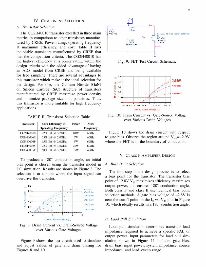
Figure 9 shows the test circuit used to simulateand adjust values of gate and drain biasing forFigures 8 and 10.
Fig. 9: FET Test Circuit Schematic
Fig. 10: Drain Current vs. Gate-Source Voltageover Various Drain Voltages
Figure 10 shows the drain current with respectto gate bias. Observe the region around VGS=−2.9Vwhere the FET is in the boundary of conduction.
V. CLASS F AMPLIFIER DESIGN
A. Bias Point Selection
The first step in the design process is to selecta bias point for the transistor. The transistor biaspoint of −2.8V Vgs maximizes efficiency, maximizesoutput power, and ensures 180° conduction angle.Both class F and class B use identical bias pointselection methods. A gate bias voltage of −2.8V isnear the cutoff point on the Id vs. Vgs plot in Figure10, which ideally results in a 180° conduction angle.
B. Load Pull Simulation
Load pull simulation determines transistor loadimpedance required to achieve a specific PAE oroutput power. Input parameters for load pull sim-ulation shown in Figure 11 include: gate bias,drain bias, input power, system impedance, sourceimpedance, and load sweep range.

7
Fig. 11: Load Pull Analysis Displaying MaximumPAE Load Impedance
Fig. 12: Load Pull Analysis PAE & Output PowerContours
The drain voltage is set to the data sheet rec-ommended 28V, and bias voltage to −2.8V as de-termined by the previous harmonic-balance sim-ulations (Figure 8) for class F operation. Inputpower is set to 27dBm and fundamental frequencyto 3.5GHz. For this specific simulation, the onlysweep parameters available are the load impedanceat the fundamental frequency and harmonic fre-quencies individually. As seen in Figure 11, theharmonic frequency load values can be set to pre-determined values while one of them is swept ata time. The real and imaginary min/max values tosweep can be set using the Z real min, Z real max,Z imag min, Z imag max respectively. Increasingthe number of ZL points (Z real num points andZ imag num points in Figure 11) and narrowing
the sweep range will increase accuracy and reso-lution, but also simulation time.
Results are displayed in contours on the ΓL planewhich outline the impedances required to achievea specific PAE or output power as seen in Figure12. Load pull simulation variants also include biaspoint sweeps and can be performed for both singleand two-tone signals that will determine a preferablebias point.
Since the source impedance is specified as oneof the simulation parameters, an iterative simulationmethod is employed. The steps for this designtechnique are as follows:
1) Set source impedance to 50Ω.2) Set gate bias to -2.8V, set drain bias to 28V,
Pavs dBm to 27.3) Set a large enough sweep range to see contours
on any location in the smith chart.4) Simulate and move black mPdel vs PAE Rho
marker to point of maximum PAE.5) Record input impedance.6) Use conjugate of the recorded input impedance
as the new source impedance.7) Repeat steps 4 through 6 until improvement
between iterations is negligible.Figure 13 shows the resulting data from the final
load pull analysis at the mPdel vs PAE marker.Expected PAE, Power Delivered, and target loadimpedance are 83.2%, 40.7W, and 6.42 + j5.26 re-spectively. The load and input impedance specifiedare the target impedances for both the input andoutput networks of the amplifier.
Fig. 13: Load Pull Amplifier Characteristics at83% PAE
C. Matching Network Design
1) Input Network: To avoid reflections at theinput and maximize PAE, the input network mustmatch the 50Ω termination to the desired sourceimpedance given by the load pull simulation done

8
Fig. 14: ADS Input Network
previously. The second and third harmonics createdby the transistor are filtered from the transistor gateto maintain a sinusoidal input, containing only thefundamental frequency. In order to design a networkthat both filters and matches, the filter is designedfirst by creating a stub filter with a matched S22 atthe harmonics. After that, the network should matchthe target ΓL to 50Ω by first translating ΓL across thefilter network. This design procedure can be doneusing a Smith chart and a simple single stub tuningmethod.
Due to the matched impedance at the 2nd and 3rd
harmonics (7GHz and 10.5GHz), seen from the tran-sistor gate, S22 is minimized at those frequencies, asseen in Figure 15, while achieving the target sourceimpedance at the fundamental.
Fig. 15: ADS Input Network |S22|
2) Output Network: Output network design issimilar to the input network. The goal is to simul-taneously control the impedances presented to thedrain of the transistor at the fundamental frequency,and the second and third harmonics. The waveshap-ing network in Figure 16 ensures the correct loadsat the harmonics.
Fig. 16: Amplifier Output Waveshaping Network
In Figure 16, the CG2H40010F transistor will re-place Term1 and the matching network will replaceTerm2. TL5 is λfund/4 at the fundamental, whichpresents an open and short circuit impedance to thetransistor at the fundamental and second harmonicsrespectively. A voltage source can be connected inparallel with the capacitor, DC Block1, to providethe VDS bias to the circuit.
TL1 and TL6 work together to provide an opencircuit for the third harmonic. TL6 is a λ3rd/4 open

9
Fig. 17: Amplifier Output Network
circuit stub at the third harmonic, which rotates toa short circuit across at the length of the stub. Thisthen rotates 3λ3rd/4 (third harmonic) across TL1 andpresents an open circuit to the transistor.
The fundamental impedance is not set to ZL
by the waveshaping network, so a matching net-work is required. The single stub matching net-work is placed after the waveshaping network sothat the fundamental impedance can be movedwithout affecting the second and third harmonicimpedances. The network will match the 50Ω loadto an impedance, ZA shown in Figure 17, whichbecomes ZL when it is translated back across thewaveshaping network. The first step to design thisis to determine the required ZA. This is done bytranslating ZL across TL1 and TL6 in Figure 17toward Term2. A single stub matching network isthen designed on a Smith chart to match the 50Ωload to the calculated ZA. The Smith chart design isshown in Appendix A, Figure 33. The waveshapingnetwork and matching network are shown togetherin Figure 17.
Fig. 18: Tuned Output Network Schematic
After the initial design is completed on the Smithchart, it is implemented in an ADS schematic usingmicrostrip lines. The electrical lengths from theSmith chart design are converted to physical lengthsusing the ADS LineCalc tool. The schematic is
then tuned using the ADS tuning tool. The tunedschematic is shown in Figure 18.
VI. SIMULATION RESULTS
A. EM SimulationElectromagnetic (EM) simulations analyze the
physical structure of a design to calculate the s-parameter response. ADS includes an EM simula-tion module, Momentum, which analyzes the inputand output network layouts. The EM simulation isset up to include the board stack-up as seen inFigure 19, input and output ports, and the frequencyplan.
Fig. 19: EM Simulation Layer Stack-up
Fig. 20: EM Simulation Port Editor
In order to simulate accurate port connections, theport editor defines reference impedance (50Γ), portlayer (Conduction Layer), and feed type (TML).Through testing we found that feed type affectsresults significantly. The transmission line (TML)feed type most closely approximates ADS piece-wise simulation.
Fig. 21: Input Network Layout
1) Input Network: The layout seen in Figure 21is simulated using Momentum. The center stub is

10
placed on the top side in order to avoid couplingbetween the first two stubs since EM simulationincludes radiation and coupling effects.
Once S-Parameters are generated, the S22 (Figure22) and impedance values are compared in TableIII. Figure 22 compares ADS piece-wise simulation(red) against Momentum results (blue) from 0 to8.5GHz. The impedance match is close to the targetΓS at the fundamental, however the network nolonger filters at the 3rd harmonic as seen in themagnitude plot.
Fig. 22: EM (red) and piece-wise (blue)Simulation Input Network |S22|
TABLE III: ADS vs. Momentum SourceImpedance Results
ADS Momentum
1.85 - j11.79 1.52 - j13.11
Discrepancies between Momentum and ADS sim-ulations can be attributed to the 62mil thickness.Via length from signal to ground introduce sig-nificant phase shift for frequencies above 8.5GHz.Changing a single via property, height, diameter, ormetal thickness, in the short circuit stub has drasticresults on the S22 response. Momentum simulationsaccount for physical dimension effects to result inaccurate network design
2) Output Network: The output network is alsosimulated in Momentum. EM simulations confirmthe ADS model. First, a layout is generated fromthe ADS schematic, as shown in Figure 23.
Fig. 24: Amplifier Output Network Momentum vs.ADS S11 Response
Fig. 23: Amplifier Output Network Layout
The S11 response is plotted on a Smith chart andis shown in Figure 24
Markers on the ADS and Momentum traces showS11 locations at the fundamental, second, and thirdharmonics. Markers do not align well between thetwo simulations. However, the two traces have thesame general shape. Therefore, the network mustbe tuned to present the correct impedances to thetransistor. This showcases why performing an EMsimulation in addition to the ADS simulations isimportant in RF design. While a network mayappear to be tuned properly in a piece wise sim-ulation, it may display different behavior in a fullwave simulation and in hardware. Since the fullwave Momentum simulation includes coupling andradiation effects, the circuit should be tuned usingthese results. However, since this project will onlybe tested in simulation, the lengths were tuned usingthe ADS simulation to give better simulation results.

11
Fig. 25: Harmonic Balance Simulation with Microstrip Components
Fig. 26: Drain Voltage FFT, Class F Amplifierwith Microstrip Components
B. Harmonic Balance Amplifier Simulation
The Harmonic Balance (HB) simulation in con-junction with an S-parameter simulation verifies theamplifier design and operation while providing finalefficiency and gain values.
The schematic in Figure 25 includes the entireamplifier design with microstrip components as ob-tained in Matching Network Design, section V-C.The DC bias point for the transistor gate and drainis −2.8V and 28V, respectively. The bias point wasselected in section V-A. Figure 26 confirms theoutput network design of a short at the secondharmonic for the drain voltage. Figure 27 displaysa short at the third harmonic for the drain current.
Fig. 27: Drain Current FFT, Class F Amplifierwith Microstrip Components
Fig. 28: Drain Voltage and Current Time Domain,Class F Amplifier with Microstrip Components
Figure 28 shows significant deviation from idealsquare and half-wave voltage and current waveform.Fourier transform of a square wave requires the third

12
Fig. 29: Amplifier |S21| at ffund, −2.8V Gate Bias
Fig. 30: Amplifier |S11| at ffund, −2.8V Gate Bias
harmonic magnitude to be 13
of the fundamental.Figure 26 shows a fundamental and third harmonicmagnitude of 16.5V and 4.0V, respectively, a ratioof 1
4. Furthermore, since the drain current should
reflect a half-wave rectified sinusoid, the drain cur-rent’s second harmonic should be proportional tothe fundamental by 4
3π≈ 0.424. Figure 27 shows
fundamental and second harmonic magnitude of1.65A and 0.35A, respectively, for a ratio of only0.212. Since harmonic control includes up the thirdharmonic and the third harmonic does not meetexpected values, addition tuning is required.
Power probe components in ADS detected aninput power of 236mW, less than the 500mW(27dBm) provided by the input signal. This leadsto S-parameter simulations which justify the input
Fig. 31: Amplifier |S21| at ffund, −3.1V Gate Bias
Fig. 32: Amplifier |S11| at ffund, −3.1V Gate Bias
power discrepancies.Figure 29 displays amplifier |S21| values of port
1 as the input and port 2 as the load. Figure 30displays amplifier input reflection |S11|. At the op-erating frequency of 3.5GHz, an |S11| of −2.413dBrepresents 57.3% reflected power. This justifies theinput power difference noted in HB simulation. Fig-ure 29 displays an amplifier |S21| plot. At 3.5GHz,the simulated gain is 16.7dB, greater than thedesired minimum gain of 13dB. Interestingly, theforward gain peak (and subsequently decrease ininput reflection) is located at 3.48GHz.
Gate bias adjustment to −3.1V resulted 80.78%efficiency and 15.913dB of forward gain (see Figure31). This adjustment also yielded an |S11| localminima at 3.5GHz (Figure 32).

13
VII. RESULTS
A power amplifier design comparable to IMScontest winners, requires minimum PAE and outputpower. Project results in Table IV show amplifierperformance over a range of bias points. At −3.1Vbias, PAE is 80.8%, just greater the 80% minimum.Power output is 9W (39.5dBm) which is well overthe 4W (36dBm) requirement. A 15.91dB gainmeets the 13dB minimum. The gate bias was revisedfrom −2.8V to −3.1V. If system is redesigned at thisrevised bias level, improved performance could beattained.
TABLE IV: Power Amplifier Design Results
Gate DC Input OutputBias Power Power Power Efficiency Gain(V) (W) (mW) (W) (dB)
-2.8 11.613 236 9.127 76.56% 16.700-2.9 11.325 242 9.081 78.05% 17.062-3.0 11.057 249 9.041 79.52% 17.173-3.1 10.826 256 9.001 80.78% 15.913-3.2 10.654 263 8.951 81.55% 4.959
With these performance metrics, the figure ofmerit for this design is 110.5, exceeding all IMScontest winner from 2006 to 2014 (See Figure 1).However, while parasitics and physical characteris-tics dimensions were included in simulation, actualresults might degrade if the design is fabricated andtested.
VIII. IMPROVEMENTS/FUTURE ENDEAVORS
The simulation results performed on this projectwere promising for a high performance RF am-plifier. However, design process refinements couldimprove results and ensure proper operation whenfabricated.
It is recommended that future project teams opti-mize gate bias as the initial design step to maximizePAE. While the −2.8V gate bias places the transistorin the knee region, this does not optimize efficiencyand gain. Determining the optimal point improvesoverall system performance, as seen in Table IV.
The input and output network design could beimproved in future projects. In this project, theinput wave shaping network is designed to filter outall harmonics generated by the transistor. However,performance might be improved if the harmonicswere shorted to ground instead of filtered. This
creates destructive interference at the transistor gate,and ensures only fundamental frequency power ex-ists at the transistor. Also, further input networktuning would improve input matching and reducesource input reflection. The output network match-ing performance at the third harmonic should berefined to produce the desired power ratio. This willimprove efficiency by reducing overlap of voltageand current waveforms.
In addition to improving the design methodology,the design process could be improved by performingMomentum EM simulations earlier and more often.Tuning the physical layout, as opposed to schematic.The importance of this step was seen in the EMsimulation of the output network that did not meetexpectations.
Lastly, implementing this design in hardware willvalidate the design method, design process, and sim-ulations. The simulation results show an amplifierthat meets all design requirements, but performancecould be improved with further work.
REFERENCES
[1] Santa Rosa, CA, USA. Keysight.(2019) [Online]. Available:https://www.keysight.com/us/en/products/software/pathwave-design-software/pathwave-advanced-design-system.html,Accessed on: Feb. 12, 2020.
[2] G. Eason, B. Noble, and I. N. Sneddon, “On certain integrals ofLipschitz-Hankel type involving products of Bessel functions,”Philosophical Transactions of the Royal Society of London.Series A, Mathematical and Physical Sciences, vol. 247, pp.529–551, April 1955.
[3] https://www.electronics-tutorials.ws/amplifier/amplifier-classes.html
[4] P. B. Kenington, High-linearity RF amplifier design. MiltonKeynes, UK: Lightning Source UK Lts., 2010.
[5] https://www.electrical4u.net/electrical-basic/use-knee-point-voltage/
[6] S. C. Cripps, RF power amplifiers for wireless communications.Boston: Artech House, 2006.

14
APPENDIX AFIGURES
Fig. 33: Amplifier Output Network Smith Chart Design

15
APPENDIX BSENIOR PROJECT ANALYSIS
Project Title: RF Power Amplifier
Student Names: Andrew FergusonAngel DelgadoRachanon Wajanakunakorn
Advisor’s Name: Dr. Dean Arakaki
Summary of Functional RequirementsIn order to fabricate a power amplifier that would be able to compete in the International Microwave
Symposium, competition requirements needed to be met while meeting performance characteristicssimilar to previous competition winners. Therefore, this project required: minimum 13dB gain, 4-40Woutput power, 80% Power Added Efficiency, and -30dBc spur at minimum output power. In order tohave access to components optimized to operate at our target frequency, the frequency of operation forthis project was selected to be 3.5GHz.
Primary ConstraintsThe main constraint we needed to consider when deciding design requirements for an RF power
amplifier was access to lab equipment which would be able to test at a high enough frequency. Most of thelab equipment we had access to could only support frequencies below 5GHz, constraining our frequencyof operation. The second constraint we faced was the access to high power, high frequency transistorsdue to the high price point. In the end, we were constrained to a transistor that CREE could provide for free.
Economic ImpactHuman Capital - The RF amplifier will create many jobs in engineering, manufacturing and sales. The
group will hire engineers, sales people, and manufacturing technicians to assist in bringing the product tomarket. On top of the direct impact, the increased performance will allow a small boost in the industriesthat use it, creating even more secondary jobs.
Financial Capital - The increased performance of the RF power amplifier will draw customers frommany industries. This will cause a large demand for the product, which will justify its high price. Therefore,the device will be very lucrative and create a lot of financial capital.
Natural Capital - The RF power amplifier uses semiconductor materials and printed circuit boards,which use harsh chemicals in manufacturing. These chemicals can cause negative effects if released intonatural environments. The group will ensure proper use of chemicals and potentially produce circuit boardsby milling instead of photolithography to cut down on chemical use.
Cost and Timing - While still in early development, initial cost targets have been made for the RFpower amplifier. A cost of 1500USD will place the product in an aggressive sales position, with its listof engineering specs. In order to allow wholesale at this price, the product must be manufactured under1000USD. Therefore, the cost of components will be tracked through development. The product is set tobe sold in August of 2020. Therefore, development must be completed by June of that year.
If manufactured on a commercial basis:Estimated number of devices/year: 565Estimated manufacturing cost per device: $1000Estimated purchase price per device: $1500Estimated profit per year: $282,500Estimated cost for user to operate devices: $0.02/Hr

16
EnvironmentalSince this project focused on simulation, environmental impacts only included electricity. The carbon
footprint is dependant on the energy source. In 2018, California generated less than 1% of electricalenergy from oil or coal. This further reduces the project’s environmental impact. However, if this projectwere to proceed to fabrication of boards, there would be environmental impacts related to that process:
What environment impacts are associated with manufacturing or use of the product?The RF power amplifier has negative environmental impacts due to its use of semiconductors and
printed circuit boards. However, current technology also uses these materials, so the addition of the RFpower amplifier to the market will have no impact on the overall environmental burden of communicationsystems. On top of this, the RF power amplifier will excel in efficiency, which will save energy in thesesystems. This will have a positive impact on the environment.
Which natural resources and ecosystem services does the project (directly and indirectly) improve orharm?
The RF power amplifier uses semiconductors, which are mined materials. This places a burden onthe environments surrounding these mines, and can negatively impact the ecosystem around it. However,these materials are very abundant on Earth and therefore, there is little risk of depleting the resource. Theamplifier also requires electrical energy to run, which could be generated from a non renewable source.This can be fixed by using more renewable energy generation methods.
Does the project impact other species?The RF power amplifier can affect the ecosystem of the areas around where the raw materials are
mined. This can negatively impact plant and animal life in the area and reduce the biodiversity of anarea if species are forced away.
ManufacturabilityThe RF power amplifier could be very easily manufactured using traditional printed circuit board
techniques. The product would be simply developed and sold as a PCB, so would use a photolithographyor milling process for board manufacturing and reflow soldering process for attaching components to theboard. Much of this can be automated, decreasing the cost in the long term.
SustainabilityThe RF power amplifier will be a very low maintenance component of a larger RF system. After initial
integration, the amplifier should not need maintenance. If there is an issue with the device, the wholeamplifier will be replaced, meaning that there is no direct maintenance. The amplifier should also be areliable component since the base components that build up to it are all reliable.
The RF power amplifier impacts the sustainable use of resources because it uses raw materials whichare non renewable such as semiconductors. While it does make use of these materials, current technologythat the amplifier would replace also use the same materials. Therefore, there is no net effect on theconsumption of non renewable raw materials. However, the amplifier will reduce the energy consumptionof systems it is in, resulting in less energy resources being used.
The design on the RF power amplifier would be improved if it were designed to be more broadbandthan it currently is. While the amplifier will be very high performance compared to other competingdesigns, its usefulness is limited by the fact that it can only be used at a very specific frequency.
To move to a more broadband design, a different amplifier topology would need to be used. The currentdesign uses components sized for a very specific frequency, and cannot be changed to make it broadband.To increase the operating range of the device, much more design would be needed.

17
EthicalWhile the applications for RF amplifiers most often include RF communication services for the public
such as phone and radio services, private communications, and satellite communications, there are highfrequency applications that can be borderline unethical. When the average individual thinks of wireless,they will probably think of our ability to communicate wirelessly through electromagnetic waves in space.However, they may not think about the side of wireless that actually causes damage to materials. On asmall scale, microwaves essentially bombard your cold food with high powered 2.4GHz waves which sohappens to be the same resonance frequency as water. This will cause the water molecules to vibrate andlead to a buildup of energy, and boiling. On a larger scale, a pulse of EM waves set off by a maliciousindividual can fry all electronics in a radius of the pulse. This is also known by the military as an EMP(Electromagnetic Pulse Attack). While wireless can be used in a safe and useful way, it can also be usedfor malicious attacks that can range from damage to people and properties.
One such example is the U.S government’s Active Denial System. This device uses millimeter waveswith a short enough wavelength that it will not penetrate a person’s skin more than a 1/64th of an inchin order to radiate a ‘man-sized’ beam that will induce a burning sensation from a range of up to 1,000meters that will instinctively cause crowds to move out of the way and disperse. While it is true thatthe waves at about 94GHz will not have the same effect as a 2.4GHz microwave oven on a person, thewaves still literally cause people’s skin to burn immediately but the government claims that because theperson will move out of the way instinctively, it is not a dangerous weapon. They also claim that anydamage caused by this weapon is ‘reversible’, which can be said for just about anything but a 3rd degreeburn. In the case of the Active Denial System, RF Power Amplifiers are being used in a way that webelieve to be unethical and go against our moral values. We believe that while we cannot control the useof our product in these unethical applications, we will not sell or support and individual or company thatcomes into possession of one of our amplifiers.
Health and SafetyThe health concerns surrounding out product ultimately come down to the customer use case and
product application. While the direct use of our product cannot harm a person directly, it can be used toradiate signals which can be of concern to public safety. The power rating at which our amplifier willoperate will only be harmful if used to transmit frequencies such as 2.4GHz while in direct proximityof the public. At max power (40W) this frequency could have harmful effects if not shielded correctly.One way companies avoid such effects is by modulating signals to different frequencies and keeping anytransmitters far away from populated areas as well as directional shielding.
Social and PoliticalDepending on our market choice, there are political implications surrounding this product in regards to
the governmental defense sector aid that it could provide. Selling this product to the government couldtie our design efforts to any kind of action the military decides to use the amplifier for. Any direct orindirect action taken as an effect of a communications system or direct military weapon in which thisdevice is used could be seen as our direct effort to strengthen the U.S military. However, any effortstowards the greater connectivity of our country as a whole with the goal of creating a more integratedsociety would therefore further our cause by introducing more efficient and powerful communicationtechnology in order to help the U.S spearhead the next generation of mobile networking.
DevelopmentThe team learned several new tools during the course of the project. Keysight’s Advanced Design
System was used heavily throughout the project, which gave the team exposure to an industry standardRF design and simulation tool. On top of this, the team gained experience with a PCB milling machinewhen working on prototypes of the design. Lastly, the team used Overleaf, which is an online LaTexediting software to write the final report.