LM1244LM2244LM3244LM2902 Low Power Quad Operational Amplifiers General Description
16
TL/H/9299 LM124/LM224/LM324/LM2902 Low Power Quad Operational Amplifiers December 1994 LM124/LM224/LM324/LM2902 Low Power Quad Operational Amplifiers General Description The LM124 series consists of four independent, high gain, internally frequency compensated operational amplifiers which were designed specifically to operate from a single power supply over a wide range of voltages. Operation from split power supplies is also possible and the low power sup- ply current drain is independent of the magnitude of the power supply voltage. Application areas include transducer amplifiers, DC gain blocks and all the conventional op amp circuits which now can be more easily implemented in single power supply sys- tems. For example, the LM124 series can be directly operat- ed off of the standard a5V power supply voltage which is used in digital systems and will easily provide the required interface electronics without requiring the additional g15V power supplies. Unique Characteristics Y In the linear mode the input common-mode voltage range includes ground and the output voltage can also swing to ground, even though operated from only a sin- gle power supply voltage Y The unity gain cross frequency is temperature compensated Y The input bias current is also temperature compensated Advantages Y Eliminates need for dual supplies Y Four internally compensated op amps in a single package Y Allows directly sensing near GND and V OUT also goes to GND Y Compatible with all forms of logic Y Power drain suitable for battery operation Features Y Internally frequency compensated for unity gain Y Large DC voltage gain 100 dB Y Wide bandwidth (unity gain) 1 MHz (temperature compensated) Y Wide power supply range: Single supply 3V to 32V or dual supplies g1.5V to g16V Y Very low supply current drain (700 mA)—essentially in- dependent of supply voltage Y Low input biasing current 45 nA (temperature compensated) Y Low input offset voltage 2 mV and offset current 5 nA Y Input common-mode voltage range includes ground Y Differential input voltage range equal to the power sup- ply voltage Y Large output voltage swing 0V to V a b 1.5V Connection Diagram Dual-In-Line Package TL/H/9299 – 1 Top View Order Number LM124J, LM124AJ, LM124J/883**, LM124AJ/883*, LM224J, LM224AJ, LM324J, LM324M, LM324AM, LM2902M, LM324N, LM324AN or LM2902N See NS Package Number J14A, M14A or N14A TL/H/9299 – 32 Order Number LM124AE/883 or LM124E/883 See NS Package Number E20A TL/H/9299 – 33 Order Number LM124AW/883 or LM124W/883 See NS Package Number W14B *LM124A available per JM38510/11006 **LM124 available per JM38510/11005 C1995 National Semiconductor Corporation RRD-B30M115/Printed in U. S. A.
-
Upload
independent -
Category
Documents
-
view
5 -
download
0
Transcript of LM1244LM2244LM3244LM2902 Low Power Quad Operational Amplifiers General Description

TL/H/9299
LM
124/LM
224/LM
324/LM
2902
Low
Pow
erQ
uad
Opera
tionalA
mplifie
rs
December 1994
LM124/LM224/LM324/LM2902Low Power Quad Operational Amplifiers
General DescriptionThe LM124 series consists of four independent, high gain,
internally frequency compensated operational amplifiers
which were designed specifically to operate from a single
power supply over a wide range of voltages. Operation from
split power supplies is also possible and the low power sup-
ply current drain is independent of the magnitude of the
power supply voltage.
Application areas include transducer amplifiers, DC gain
blocks and all the conventional op amp circuits which now
can be more easily implemented in single power supply sys-
tems. For example, the LM124 series can be directly operat-
ed off of the standard a5V power supply voltage which is
used in digital systems and will easily provide the required
interface electronics without requiring the additional g15V
power supplies.
Unique CharacteristicsY In the linear mode the input common-mode voltage
range includes ground and the output voltage can also
swing to ground, even though operated from only a sin-
gle power supply voltageY The unity gain cross frequency is temperature
compensatedY The input bias current is also temperature
compensated
AdvantagesY Eliminates need for dual suppliesY Four internally compensated op amps in a single
packageY Allows directly sensing near GND and VOUT also goes
to GNDY Compatible with all forms of logicY Power drain suitable for battery operation
FeaturesY Internally frequency compensated for unity gainY Large DC voltage gain 100 dBY Wide bandwidth (unity gain) 1 MHz
(temperature compensated)Y Wide power supply range:
Single supply 3V to 32V
or dual supplies g1.5V to g16VY Very low supply current drain (700 mA)Ðessentially in-
dependent of supply voltageY Low input biasing current 45 nA
(temperature compensated)Y Low input offset voltage 2 mV
and offset current 5 nAY Input common-mode voltage range includes groundY Differential input voltage range equal to the power sup-
ply voltageY Large output voltage swing 0V to Va b 1.5V
Connection Diagram
Dual-In-Line Package
TL/H/9299–1
Top View
Order Number LM124J, LM124AJ, LM124J/883**,
LM124AJ/883*, LM224J, LM224AJ, LM324J, LM324M,
LM324AM, LM2902M, LM324N, LM324AN or LM2902N
See NS Package Number J14A, M14A or N14A
TL/H/9299–32
Order Number LM124AE/883 or LM124E/883
See NS Package Number E20A
TL/H/9299–33
Order Number LM124AW/883 or LM124W/883
See NS Package Number W14B*LM124A available per JM38510/11006
**LM124 available per JM38510/11005
C1995 National Semiconductor Corporation RRD-B30M115/Printed in U. S. A.

Absolu
teM
axim
um
Ratings
IfM
ilitary
/A
ero
space
specifie
ddevic
es
are
required,ple
ase
conta
ct
the
NationalSem
iconducto
rSale
sO
ffic
e/D
istr
ibuto
rsfo
ravailability
and
specific
ations.
(Note
9)
LM
124/LM
224/LM
324
LM
2902
LM
124/LM
224/LM
324
LM
2902
LM
124A
/LM
224A
/LM
324A
LM
124A
/LM
224A
/LM
324A
Supply
Voltage,V
a
32V
26V
Sto
rage
Tem
pera
ture
Range
b65§C
toa
150§C
b65§C
toa
150§C
Diffe
rentialI
nputVoltage
32V
26V
Lead
Tem
pera
ture
(Sold
ering,10
seconds)
260§C
260§C
InputVoltage
b0.3
Vto
a32V
b0.3
Vto
a26V
Sold
ering
Info
rmation
Dual-In
-Lin
ePackage
InputC
urrent
Sold
ering
(10
seconds)
260§C
260§C
(VIN
kb
0.3
V)(N
ote
3)
50
mA
50
mA
Sm
all
Outlin
ePackage
Pow
erD
issip
ation
(Note
1)
VaporPhase
(60
seconds)
215§C
215§C
Mold
ed
DIP
1130
mW
1130
mW
Infrare
d(1
5seconds)
220§C
220§C
Cavity
DIP
1260
mW
1260
mW
See
AN
-450
‘‘Surface
Mounting
Meth
ods
and
Their
Effecton
Pro
ductR
elia
bility
’’fo
rSm
all
Outlin
ePackage
800
mW
800
mW
oth
erm
eth
ods
ofsold
ering
surface
mountdevic
es.
Outp
utShort-C
ircuit
toG
ND
ESD
Tole
rance
(Note
10)
250V
250V
(One
Am
plif
ier)
(Note
2)
Va
s15V
and
TA
e25§C
Continuous
Continuous
Opera
ting
Tem
pera
ture
Range
b40§C
toa
85§C
LM
324/LM
324A
0§C
toa
70§C
LM
224/LM
224A
b25§C
toa
85§C
LM
124/LM
124A
b55§C
toa
125§C
Ele
ctr
icalC
hara
cte
ristics
Va
ea
5.0
V,(N
ote
4),
unle
ss
oth
erw
ise
sta
ted
Para
mete
rC
onditio
ns
LM
124A
LM
224A
LM
324A
LM
124/LM
224
LM
324
LM
2902
Units
Min
Typ
Max
Min
Typ
Max
Min
Typ
Max
Min
Typ
Max
Min
Typ
Max
Min
Typ
Max
InputO
ffsetVoltage
(Note
5)T
Ae
25§C
12
13
23
25
27
27
mV
InputB
ias
Current
I IN
(a)orI IN
(b),
VC
Me
0V,
20
50
40
80
45
100
45
150
45
250
45
250
nA
(Note
6)
TA
e25§C
InputO
ffsetC
urrent
I IN
(a)b
I IN
(b),
VC
Me
0V,
210
215
530
330
550
550
nA
TA
e25§C
InputC
om
mon-M
ode
Va
e30V,(L
M2902,V
ae
26V),
0V
ab
1.5
0V
ab
1.5
0V
ab
1.5
0V
ab
1.5
0V
ab
1.5
0V
ab
1.5
VVoltage
Range
(Note
7)
TA
e25§C
Supply
Current
OverFull
Tem
pera
ture
Range
RL
e%
On
All
Op
Am
ps
mA
Va
e30V
(LM
2902
Va
e26V)
1.5
31.5
31.5
31.5
31.5
31.5
3
Va
e5V
0.7
1.2
0.7
1.2
0.7
1.2
0.7
1.2
0.7
1.2
0.7
1.2
Larg
eSig
nal
Va
e15V,R
Lt
2kX
,50
100
50
100
25
100
50
100
25
100
25
100
V/m
VVoltage
Gain
(VO
e1V
to11V),
TA
e25§C
Com
mon-M
ode
DC
,V
CM
e0V
toV
ab
1.5
V,
70
85
70
85
65
85
70
85
65
85
50
70
dB
Reje
ction
Ratio
TA
e25§C
Pow
erSupply
Va
e5V
to30V
Reje
ction
Ratio
(LM
2902,V
ae
5V
to26V),
65
100
65
100
65
100
65
100
65
100
50
100
dB
TA
e25§C
2

Ele
ctr
icalC
hara
cte
ristics
Va
ea
5.0
V(N
ote
4)unle
ss
oth
erw
ise
sta
ted
(Continued)
Para
mete
rC
onditio
ns
LM
124A
LM
224A
LM
324A
LM
124/LM
224
LM
324
LM
2902
Units
Min
Typ
Max
Min
Typ
Max
Min
Typ
Max
Min
Typ
Max
Min
Typ
Max
Min
Typ
Max
Am
plif
ier-to
-Am
plif
ier
fe
1kH
zto
20
kH
z,T
Ae
25§C
b120
b120
b120
b120
b120
b120
dB
Couplin
g(N
ote
8)
(InputR
efe
rred)
Outp
utC
urrent
Sourc
eV
INa
e1V,V
INb
e0V,
20
40
20
40
20
40
20
40
20
40
20
40
Va
e15V,V
Oe
2V,T
Ae
25§C
mA
Sin
kV
INb
e1V,V
INa
e0V,
10
20
10
20
10
20
10
20
10
20
10
20
Va
e15V,V
Oe
2V,T
Ae
25§C
VIN
be
1V,V
INa
e0V,
12
50
12
50
12
50
12
50
12
50
12
50
mA
Va
e15V,V
Oe
200
mV,T
Ae
25§C
Short
Circuit
toG
round
(Note
2)V
ae
15V,T
Ae
25§C
40
60
40
60
40
60
40
60
40
60
40
60
mA
InputO
ffsetVoltage
(Note
5)
44
57
910
mV
InputO
ffset
RS
e0X
720
720
730
77
7m
V/§C
Voltage
Drift
InputO
ffsetC
urrent
I IN
(a)b
I IN
(b),
VC
Me
0V
30
30
75
100
150
45
200
nA
InputO
ffset
RS
e0X
10
200
10
200
10
300
10
10
10
pA
/§C
CurrentD
rift
InputB
ias
Current
I IN
(a)orI IN
(b)
40
100
40
100
40
200
40
300
40
500
40
500
nA
InputC
om
mon-M
ode
Va
ea
30V
0V
ab
20
Va
b2
0V
ab
20
Va
b2
0V
ab
20
Va
b2
VVoltage
Range
(Note
7)
(LM
2902,V
ae
26V)
Larg
eSig
nal
Va
ea
15V
Voltage
Gain
(VO
Sw
ing
e1V
to11V)
25
25
15
25
15
15
V/m
V
RL
t2
kX
Outp
utVoltage
VO
HV
ae
30V
RL
e2
kX
26
26
26
26
26
22
VSw
ing
(LM
2902,V
ae
26V)
RL
e10
kX
27
28
27
28
27
28
27
28
27
28
23
24
VO
LV
ae
5V,R
Le
10
kX
520
520
520
520
520
5100
mV
3
Ele
ctr
icalC
hara
cte
ristics
Va
ea
5.0
V(N
ote
4)unle
ss
oth
erw
ise
sta
ted
(Continued)
Para
mete
rC
onditio
ns
LM
124A
LM
224A
LM
324A
LM
124/LM
224
LM
324
LM
2902
Units
Min
Typ
Max
Min
Typ
Max
Min
Typ
Max
Min
Typ
Max
Min
Typ
Max
Min
Typ
Max
Outp
utC
urrent
Sourc
eV
Oe
2V
VIN
ae
a1V,
10
20
10
20
10
20
10
20
10
20
10
20
VIN
be
0V,V
ae
15V
mA
Sin
kV
INb
ea
1V,
10
15
58
58
58
58
58
VIN
ae
0V,V
ae
15V
Note
1:Foropera
ting
athig
hte
mpera
ture
s,th
eLM
324/LM
324A
/LM
2902
mustbe
dera
ted
based
on
aa
125§C
maxim
um
junction
tem
pera
ture
and
ath
erm
alre
sis
tance
of88§C
/W
whic
happlie
sfo
rth
edevic
esold
ere
din
aprinte
d
circuit
board
,opera
ting
ina
still
air
am
bie
nt.
The
LM
224/LM
224A
and
LM
124/LM
124A
can
be
dera
ted
based
on
aa
150§C
maxim
um
junction
tem
pera
ture
.The
dis
sip
ation
isth
eto
talofall
fouram
plif
iers
Ðuse
exte
rnalre
sis
tors
,
where
possib
le,to
allo
wth
eam
plif
ierto
satu
rate
ofto
reduce
the
pow
erw
hic
his
dis
sip
ate
din
the
inte
gra
ted
circuit.
Note
2:Short
circuits
from
the
outp
utto
Va
can
cause
excessiv
eheating
and
eventu
aldestruction.W
hen
consid
ering
short
circuits
togro
und,th
em
axim
um
outp
utcurrentis
appro
xim
ate
ly40
mA
independentofth
em
agnitude
of
Va
.A
tvalu
es
ofsupply
voltage
inexcess
of
a15V,continuous
short-c
ircuits
can
exceed
the
pow
erdis
sip
ation
ratings
and
cause
eventu
aldestruction.D
estructive
dis
sip
ation
can
result
from
sim
ultaneous
shorts
on
all
am
plif
iers
.
Note
3:This
inputcurrentw
illonly
exis
tw
hen
the
voltage
atany
ofth
ein
putle
ads
isdriven
negative.It
isdue
toth
ecolle
cto
r-base
junction
ofth
ein
putPN
Ptransis
tors
becom
ing
forw
ard
bia
sed
and
there
by
acting
as
inputdio
de
cla
mps.In
additio
nto
this
dio
de
action,th
ere
isals
ola
tera
lN
PN
para
sitic
transis
toraction
on
the
ICchip
.This
transis
toraction
can
cause
the
outp
utvoltages
ofth
eop
am
ps
togo
toth
eV
a
voltage
level(o
rto
gro
und
fora
larg
e
overd
rive)fo
rth
etim
edura
tion
thatan
inputis
driven
negative.This
isnotdestructive
and
norm
aloutp
utsta
tes
will
re-e
sta
blis
hw
hen
the
inputvoltage,w
hic
hw
as
negative,again
retu
rns
toa
valu
egre
ate
rth
an
b0.3
V(a
t25§C
).
Note
4:These
specific
ations
are
limited
tob
55§C
sT
As
a125§C
for
the
LM
124/LM
124A
.W
ith
the
LM
224/LM
224A
,all
tem
pera
ture
specific
ations
are
limited
tob
25§C
sT
As
a85§C
,th
eLM
324/LM
324A
tem
pera
ture
specific
ations
are
limited
to0§C
sT
As
a70§C
,and
the
LM
2902
specific
ations
are
limited
tob
40§C
sT
As
a85§C
.
Note
5:V
Oj
1.4
V,R
Se
0X
with
Va
from
5V
to30V;and
overth
efu
llin
putcom
mon-m
ode
range
(0V
toV
ab
1.5
V)fo
rLM
2902,V
a
from
5V
to26V.
Note
6:The
direction
ofth
ein
putcurrentis
outofth
eIC
due
toth
ePN
Pin
putsta
ge.This
currentis
essentially
consta
nt,
independentofth
esta
teofth
eoutp
utso
no
loadin
gchange
exis
tson
the
inputlin
es.
Note
7:The
inputcom
mon-m
ode
voltage
ofeitherin
putsig
nalvoltage
should
notbe
allo
wed
togo
negative
by
more
than
0.3
V(a
t25§C
).The
upperend
ofth
ecom
mon-m
ode
voltage
range
isV
ab
1.5
V(a
t25§C
),buteitherorboth
inputs
can
go
toa
32V
withoutdam
age
(a26V
forLM
2902),
independentofth
em
agnitude
ofV
a
.
Note
8:D
ue
topro
xim
ity
ofexte
rnalcom
ponents
,in
sure
thatcouplin
gis
notorigin
ating
via
stray
capacitance
betw
een
these
exte
rnalparts.This
typic
ally
can
be
dete
cte
das
this
type
ofcapacitance
incre
ases
athig
herfrequencie
s.
Note
9:R
efe
rto
RETS124A
Xfo
rLM
124A
milita
ryspecific
ations
and
refe
rto
RETS124X
forLM
124
milita
ryspecific
ations.
Note
10:H
um
an
body
model,
1.5
kX
inseries
with
100
pF.
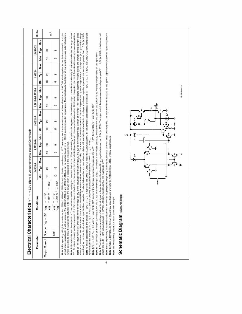
Schem
atic
Dia
gra
m(E
ach
Am
plif
ier)
TL/H
/9299–2
4

Typical Performance Characteristics
Input Voltage Range Input Current Supply Current
Voltage Gain Response
Open Loop Frequency
Ratio
Common Mode Rejection
Response
Voltage Follower Pulse
Response (Small Signal)
Voltage Follower Pulse
Response
Large Signal Frequency
Current Sourcing
Output Characteristics
Current Sinking
Output Characteristics
Current Limiting
TL/H/9299–3
5

Typical Performance Characteristics (LM2902 only)
Input Current Voltage Gain
TL/H/9299–4
Application HintsThe LM124 series are op amps which operate with only a
single power supply voltage, have true-differential inputs,
and remain in the linear mode with an input common-mode
voltage of 0 VDC. These amplifiers operate over a wide
range of power supply voltage with little change in perform-
ance characteristics. At 25§C amplifier operation is possible
down to a minimum supply voltage of 2.3 VDC.
The pinouts of the package have been designed to simplify
PC board layouts. Inverting inputs are adjacent to outputs
for all of the amplifiers and the outputs have also been
placed at the corners of the package (pins 1, 7, 8, and 14).
Precautions should be taken to insure that the power supply
for the integrated circuit never becomes reversed in polarity
or that the unit is not inadvertently installed backwards in a
test socket as an unlimited current surge through the result-
ing forward diode within the IC could cause fusing of the
internal conductors and result in a destroyed unit.
Large differential input voltages can be easily accommo-
dated and, as input differential voltage protection diodes are
not needed, no large input currents result from large differ-
ential input voltages. The differential input voltage may be
larger than Va without damaging the device. Protection
should be provided to prevent the input voltages from going
negative more than b0.3 VDC (at 25§C). An input clamp
diode with a resistor to the IC input terminal can be used.
To reduce the power supply drain, the amplifiers have a
class A output stage for small signal levels which converts
to class B in a large signal mode. This allows the amplifiers
to both source and sink large output currents. Therefore
both NPN and PNP external current boost transistors can
be used to extend the power capability of the basic amplifi-
ers. The output voltage needs to raise approximately 1 di-
ode drop above ground to bias the on-chip vertical PNP
transistor for output current sinking applications.
For ac applications, where the load is capacitively coupled
to the output of the amplifier, a resistor should be used, from
the output of the amplifier to ground to increase the class A
bias current and prevent crossover distortion.
Where the load is directly coupled, as in dc applications,
there is no crossover distortion.
Capacitive loads which are applied directly to the output of
the amplifier reduce the loop stability margin. Values of
50 pF can be accommodated using the worst-case non-in-
verting unity gain connection. Large closed loop gains or
resistive isolation should be used if larger load capacitance
must be driven by the amplifier.
The bias network of the LM124 establishes a drain current
which is independent of the magnitude of the power supply
voltage over the range of from 3 VDC to 30 VDC.
Output short circuits either to ground or to the positive pow-
er supply should be of short time duration. Units can be
destroyed, not as a result of the short circuit current causing
metal fusing, but rather due to the large increase in IC chip
dissipation which will cause eventual failure due to exces-
sive junction temperatures. Putting direct short-circuits on
more than one amplifier at a time will increase the total IC
power dissipation to destructive levels, if not properly pro-
tected with external dissipation limiting resistors in series
with the output leads of the amplifiers. The larger value of
output source current which is available at 25§C provides a
larger output current capability at elevated temperatures
(see typical performance characteristics) than a standard IC
op amp.
The circuits presented in the section on typical applications
emphasize operation on only a single power supply voltage.
If complementary power supplies are available, all of the
standard op amp circuits can be used. In general, introduc-
ing a pseudo-ground (a bias voltage reference of Va
/2) will
allow operation above and below this value in single power
supply systems. Many application circuits are shown which
take advantage of the wide input common-mode voltage
range which includes ground. In most cases, input biasing is
not required and input voltages which range to ground can
easily be accommodated.
6

Typical Single-Supply Applications (Va
e 5.0 VDC)
Non-Inverting DC Gain (0V Input e 0V Output)
TL/H/9299–5
*R not needed due to temperature
independent IIN
DC Summing Amplifier
(VIN’S t 0 VDC and VO t VDC)
TL/H/9299–6
Where: VO e V1 a V2 b V3 b V4
(V1 a V2) t (V3 a V4) to keep VO l 0 VDC
Power Amplifier
VO e 0 VDC for VIN e 0 VDC
AV e 10
TL/H/9299–7
LED Driver
TL/H/9299–8
‘‘BI-QUAD’’ RC Active Bandpass Filter
fo e 1 kHz
Q e 50
AV e 100 (40 dB)
TL/H/9299–9
7

Typical Single-Supply Applications (Va
e 5.0 VDC) (Continued)
Fixed Current Sources
TL/H/9299–10I2 e #R1
R2 J I1
Lamp Driver
TL/H/9299–11
Current Monitor
VO e
1V(IL)
1A
VL s Va
b 2V
*(Increase R1 for IL small)
TL/H/9299–12
Driving TTL
TL/H/9299–13
Voltage Follower
VO e VIN
TL/H/9299–14
Pulse Generator
TL/H/9299–15
8

Typical Single-Supply Applications (Va
e 5.0 VDC) (Continued)
Squarewave Oscillator
TL/H/9299–16
Pulse Generator
TL/H/9299–17
High Compliance Current Sink
IO e 1 amp/volt VIN
(Increase RE for Io small) TL/H/9299–18
Low Drift Peak Detector
HIGH ZIN
LOW ZOUT
TL/H/9299–19
Comparator with Hysteresis
TL/H/9299–20
Ground Referencing a Differential Input Signal
VO e VR
TL/H/9299–21
9

Typical Single-Supply Applications (Va
e 5.0 VDC) (Continued)
Voltage Controlled Oscillator Circuit
TL/H/9299–22
*Wide control voltage range: 0 VDC s VC s 2 (Va b1.5 VDC)
Photo Voltaic-Cell Amplifier
TL/H/9299–23
AC Coupled Inverting Amplifier
TL/H/9299–24
AV e
Rf
R1(As shown, AV e 10)
10

Typical Single-Supply Applications (Va
e 5.0 VDC) (Continued)
AC Coupled Non-Inverting Amplifier
TL/H/9299–25
AV e 1 a
R2
R1
AV e 11 (As shown)
DC Coupled Low-Pass RC Active Filter
TL/H/9299–26
fO e 1 kHz
Q e 1
AV e 2
High Input Z, DC Differential Amplifier
TL/H/9299–27ForR1
R2e
R4
R3(CMRR depends on this resistor ratio match)
VO e 1 a
R4
R3(V2 b V1)
As shown: VO e 2(V2 b V1)
11

Typical Single-Supply Applications (Va
e 5.0 VDC) (Continued)
High Input Z Adjustable-Gain
DC Instrumentation Amplifier
TL/H/9299–28If R1 e R5 & R3 e R4 e R6 e R7 (CMRR depends on match)
VO e 1 a
2R1
R2(V2 b V1)
As shown VO e 101 (V2 b V1)
Using Symmetrical Amplifiers to
Reduce Input Current (General Concept)
TL/H/9299–29
Bridge Current Amplifier
For e kk 1 and Rf ll R
VO j VREF # e
2 J Rf
R
TL/H/9299–30
12

Typical Single-Supply Applications (Va
e 5.0 VDC) (Continued)
Bandpass Active Filter
TL/H/9299–31
fO e 1 kHz
Q e 25
13

Physical Dimensions inches (millimeters)
Leadless Chip Carrier Package
Order Number LM124AE/883 or LM124E/883
NS Package Number E20A
Ceramic Dual-In-Line Package (J)
Order Number LM124J, LM124AJ, LM124AJ/883, LM124J/883, LM224J, LM224AJ or LM324J
NS Package Number J14A
14

Physical Dimensions inches (millimeters) (Continued)
S.O. Package (M)
Order Number LM324M, LM324AM or LM2902M
NS Package Number M14A
Molded Dual-In-Line Package (N)
Order Number LM324N, LM324AN or LM2902N
NS Package Number N14A
15

LM
124/LM
224/LM
324/LM
2902
Low
Pow
erQ
uad
Opera
tionalA
mplifiers
Physical Dimensions inches (millimeters) (Continued)
Ceramic Flatpak Package
Order Number LM124AW/883 or LM124W/883
NS Package Number W14B
LIFE SUPPORT POLICY
NATIONAL’S PRODUCTS ARE NOT AUTHORIZED FOR USE AS CRITICAL COMPONENTS IN LIFE SUPPORT
DEVICES OR SYSTEMS WITHOUT THE EXPRESS WRITTEN APPROVAL OF THE PRESIDENT OF NATIONAL
SEMICONDUCTOR CORPORATION. As used herein:
1. Life support devices or systems are devices or 2. A critical component is any component of a life
systems which, (a) are intended for surgical implant support device or system whose failure to perform can
into the body, or (b) support or sustain life, and whose be reasonably expected to cause the failure of the life
failure to perform, when properly used in accordance support device or system, or to affect its safety or
with instructions for use provided in the labeling, can effectiveness.
be reasonably expected to result in a significant injury
to the user.
National Semiconductor National Semiconductor National Semiconductor National SemiconductorCorporation Europe Hong Kong Ltd. Japan Ltd.1111 West Bardin Road Fax: (a49) 0-180-530 85 86 13th Floor, Straight Block, Tel: 81-043-299-2309Arlington, TX 76017 Email: cnjwge@ tevm2.nsc.com Ocean Centre, 5 Canton Rd. Fax: 81-043-299-2408Tel: 1(800) 272-9959 Deutsch Tel: (a49) 0-180-530 85 85 Tsimshatsui, KowloonFax: 1(800) 737-7018 English Tel: (a49) 0-180-532 78 32 Hong Kong
Fran3ais Tel: (a49) 0-180-532 93 58 Tel: (852) 2737-1600Italiano Tel: (a49) 0-180-534 16 80 Fax: (852) 2736-9960
National does not assume any responsibility for use of any circuitry described, no circuit patent licenses are implied and National reserves the right at any time without notice to change said circuitry and specifications.