
1-V rail-to-rail operational amplifiers in standard CMOS technology
12
IEEE JOURNAL OF SOLID-STATE CIRCUITS, VOL. 35, NO. 1, JANUARY 2000 33 1-V Rail-to-Rail Operational Amplifiers in Standard CMOS Technology J. Francisco Duque-Carrillo, Member, IEEE, José L. Ausín, Guido Torelli, Senior Member, IEEE, José M. Valverde, and Miguel A. Domínguez Abstract—The constraints on the design of CMOS operational amplifiers with rail-to-rail input range for extremely low supply voltage operation, are addressed. Two design approaches for amplifiers based on complementary input differential pairs and a single input pair, respectively, are presented. The first realizes a feedforward action to accommodate the common-mode (CM) component of the input signals to the amplifier input range. The second approach performs a negative feedback action over the input CM signal. Two operational amplifiers based on the proposed approaches have been designed for 1-V total supply operation, and fabricated in a standard 1.2-μm CMOS process. Experimental results are provided and the corresponding perfor- mances are discussed and compared. Index Terms—CMOS analog integrated circuits, low voltage, op- erational amplifiers, rail-to-rail operation. I. INTRODUCTION S CALING of modern integrated circuit (IC) technologies as well as the increasing importance of battery- and solar- powered systems, demand more and more circuits able to op- erate in very low supply voltage environments. However, while digital circuits can work without too many problems in such supply conditions, new analog circuit architectures must be de- veloped to keep similar performance with respect to the opera- tion at higher supply voltages. The most important basic building block in analog and mixed-mode circuits is the operational amplifier. In a well-de- signed low-voltage (LV) op-amp, the minimum supply voltage value is imposed by the differential pair of the input stage, and is equal to a threshold voltage ( ) plus two overdrive voltages ( ). For typical CMOS processes, this value turns out to be around 1 V. On the other hand, the main limitation of differential pairs consists in the reduced input common-mode (CM) range. For an n-channel input pair, this is limited to the voltage interval comprised between and ( and being the negative and the positive supply, respectively), while for a p-channel input pair it is limited between and . To avoid this Manuscript received March 11, 1999; revised July 20, 1999. This work was supported by the Spanish R&D Plan and the European Union under Grant 97-0254-C02. J. F. Duque-Carrillo, J. L. Ausín, J. M. Valverde, and M. A. Domínguez are with the Department of Electronics and Electrical Engineering, University of Extremadura, 06071 Badajoz, Spain. G. Torelli is with the Department of Electronics, University of Pavia, 27100 Pavia, Italy. Publisher Item Identifier S 0018-9200(00)00124-4. drawback, the simplest solution could consist in using ampli- fiers connected in inverting configuration (i.e., operating with a virtual ground at the inverting input terminal), nonetheless, it also has some disadvantages. In fact, the input impedance can be low and the input and output dc levels must be different. With respect to the latter point, if the amplifier input stage is an n-channel differential pair, at 1-V supply voltage for instance, the dc input CM component must be very close to the positive supply voltage, while to ensure rail-to-rail output swing, the corresponding output quiescent level should be set around the middle between the positive and the negative supply voltages. By contrast, in noninverting amplifier configurations, the constraint of the input impedance does not exist, but the amplifier input CM range must be extended up to the rails to fully exploit the very limited available voltage room. For these cases, the traditional approach [1]–[13] has consisted in using parallel-connected complementary differential pairs in the input stage as shown in Fig. 1(a). The principle of this approach is illustrated in Fig. 1(b). Basically, it consists in keeping at least one of the input pairs adequately biased for any value of the input CM voltage. Thus, for input CM voltages in the middle range [ ], both pairs are active, but if the input CM component is close to the positive [ ] or the negative [ ] supply, just the n-channel or the p-channel differential pair, respectively, is active. However, the situation is drastically different when the total supply voltage is further reduced, as shown in Fig. 1(c). Now, a forbidden amplifier operation zone arises for input CM voltages in the middle range: the input voltage is not able to turn on any transistor pair in this range, and therefore the amplifier operation is only possible for CM voltages very close to either supply rail. Recently, two design techniques have been proposed to ex- tend the input CM range in LV CMOS op-amps based on a single input differential pair. The first one [14] incorporates an on-chip voltage multiplier to provide a higher local supply voltage for the input differential pair. However, the use of voltage multi- pliers is not an effective solution in scaled technologies. An- other proposed technique [15] uses the back-gate transistor ter- minals of the amplifier differential pair to apply the input sig- nals, as in this way the signals do not necessarily have to be higher than the transistor threshold voltage. The main draw- back of this approach is that some important amplifier param- eters, such as dc gain and gain-bandwidth product, turn out to be rather low as a consequence of the low values of the MOS transistor substrate transconductance. Finally, solutions based 0018–9200/00$10.00 © 2000 IEEE
Transcript of 1-V rail-to-rail operational amplifiers in standard CMOS technology

IEEE JOURNAL OF SOLID-STATE CIRCUITS, VOL. 35, NO. 1, JANUARY 2000 33
1-V Rail-to-Rail Operational Amplifiers inStandard CMOS Technology
J. Francisco Duque-Carrillo, Member, IEEE, José L. Ausín, Guido Torelli, Senior Member, IEEE, José M. Valverde,and Miguel A. Domínguez
Abstract—The constraints on the design of CMOS operationalamplifiers with rail-to-rail input range for extremely low supplyvoltage operation, are addressed. Two design approaches foramplifiers based on complementary input differential pairs anda single input pair, respectively, are presented. The first realizesa feedforward action to accommodate the common-mode (CM)component of the input signals to the amplifier input range.The second approach performs a negative feedback action overthe input CM signal. Two operational amplifiers based on theproposed approaches have been designed for 1-V total supplyoperation, and fabricated in a standard 1.2-µm CMOS process.Experimental results are provided and the corresponding perfor-mances are discussed and compared.
Index Terms—CMOS analog integrated circuits, low voltage, op-erational amplifiers, rail-to-rail operation.
I. INTRODUCTION
SCALING of modern integrated circuit (IC) technologiesas well as the increasing importance of battery- and solar-
powered systems, demand more and more circuits able to op-erate in very low supply voltage environments. However, whiledigital circuits can work without too many problems in suchsupply conditions, new analog circuit architectures must be de-veloped to keep similar performance with respect to the opera-tion at higher supply voltages.
The most important basic building block in analog andmixed-mode circuits is the operational amplifier. In a well-de-signed low-voltage (LV) op-amp, the minimum supply voltagevalue is imposed by the differential pair of the input stage, andis equal to a threshold voltage () plus two overdrive voltages( ). For typical CMOS processes, this value turns outto be around 1 V. On the other hand, the main limitation ofdifferential pairs consists in the reduced input common-mode(CM) range. For an n-channel input pair, this is limited to thevoltage interval comprised between and
( and being the negative and the positive supply,respectively), while for a p-channel input pair it is limitedbetween and . To avoid this
Manuscript received March 11, 1999; revised July 20, 1999. This work wassupported by the Spanish R&D Plan and the European Union under Grant97-0254-C02.
J. F. Duque-Carrillo, J. L. Ausín, J. M. Valverde, and M. A. Domínguez arewith the Department of Electronics and Electrical Engineering, University ofExtremadura, 06071 Badajoz, Spain.
G. Torelli is with the Department of Electronics, University of Pavia, 27100Pavia, Italy.
Publisher Item Identifier S 0018-9200(00)00124-4.
drawback, the simplest solution could consist in using ampli-fiers connected in inverting configuration (i.e., operating witha virtual ground at the inverting input terminal), nonetheless,it also has some disadvantages. In fact, the input impedancecan be low and the input and output dc levels must be different.With respect to the latter point, if the amplifier input stageis an n-channel differential pair, at 1-V supply voltage forinstance, the dc input CM component must be very close tothe positive supply voltage, while to ensure rail-to-rail outputswing, the corresponding output quiescent level should be setaround the middle between the positive and the negative supplyvoltages. By contrast, in noninverting amplifier configurations,the constraint of the input impedance does not exist, but theamplifier input CM range must be extended up to the railsto fully exploit the very limited available voltage room. Forthese cases, the traditional approach [1]–[13] has consistedin using parallel-connected complementary differential pairsin the input stage as shown in Fig. 1(a). The principle of thisapproach is illustrated in Fig. 1(b). Basically, it consists inkeeping at least one of the input pairs adequately biased for anyvalue of the input CM voltage. Thus, for input CM voltages
in the middle range [ ], both pairs areactive, but if the input CM component is close to the positive[ ] or the negative [ ]supply, just the n-channel or the p-channel differential pair,respectively, is active. However, the situation is drasticallydifferent when the total supply voltage is further reduced, asshown in Fig. 1(c). Now, a forbidden amplifier operation zonearises for input CM voltages in the middle range: the inputvoltage is not able to turn on any transistor pair in this range,and therefore the amplifier operation is only possible for CMvoltages very close to either supply rail.
Recently, two design techniques have been proposed to ex-tend the input CM range in LV CMOS op-amps based on a singleinput differential pair. The first one [14] incorporates an on-chipvoltage multiplier to provide a higher local supply voltage forthe input differential pair. However, the use of voltage multi-pliers is not an effective solution in scaled technologies. An-other proposed technique [15] uses the back-gate transistor ter-minals of the amplifier differential pair to apply the input sig-nals, as in this way the signals do not necessarily have to behigher than the transistor threshold voltage. The main draw-back of this approach is that some important amplifier param-eters, such as dc gain and gain-bandwidth product, turn out tobe rather low as a consequence of the low values of the MOStransistor substrate transconductance. Finally, solutions based
0018–9200/00$10.00 © 2000 IEEE

34 IEEE JOURNAL OF SOLID-STATE CIRCUITS, VOL. 35, NO. 1, JANUARY 2000
(a)
(b)
(c)
Fig. 1. (a) Typical input stage for rail-to-rail amplifiers, (b) differentoperation zones for low supply voltage operation, and (c) differentoperation zones for extremely low supply voltage operation (V =
V + 2 � V + V ; V = V � 2 � jV j � jV j).
on low-threshold transistors are not very attractive, as they re-quire costly nonstandard fabrication processes [16], [17].
This paper presents two different design solutions forvery-low-voltage rail-to-rail CMOS op-amps. The first solutionis adequate for amplifiers based on complementary inputdifferential pairs. It incorporates a front-end section, whichrealizes a feedforward action to accommodate the input CMcomponent to the allowed amplifier range. The second ap-proach is suitable for amplifiers with an input stage made up ofa single differential pair. Now, the input CM signal is adaptedto the amplifier input range by means of a front-end circuitbased on a CM feedback loop. The description will be madeassuming the amplifier is driven by a low-impedance signalsource. The rest of the paper has been organized as follows. InSection II, the design of rail-to-rail CMOS amplifiers basedon complementary input differential pairs at extremely lowsupply voltages, is described and performance limitations areaddressed. Next, Section III deals with the design of rail-to-railamplifiers based on a single input differential pair for the sameoperating conditions. Experimental results of both approaches,obtained from a test chip prototype operating with 1 V of totalsupply voltage, are shown and compared in Section IV. Finally,conclusions are drawn in Section V.
II. RAIL -TO-RAIL AMPLIFIERS BASED ON COMPLEMENTARY
INPUT PAIRS AT EXTREMELY LOW SUPPLY VOLTAGES
A. Principle of Operation
For rail-to-rail amplifiers based on complementary input pairsoperating at very low voltage, the dead region of input CM volt-ages shown in Fig. 1(c), must be avoided. To overcome this lim-itation, the concept of dynamic level-shifting has been proposedfor bipolar operational amplifiers [5]. The principle of operationis illustrated in Fig. 2 and briefly described next. In this figure aswell as in the rest of the paper, is assumed to be equal to 0 V(i.e., connected to ground). A nonlinear circuit, represented bythe square box, generates a currentas a function of the inputCM voltage ( ), as shown in the square box itself. The gen-erated current reaches its maximum value ( ) for inthe middle of the total voltage range, while it decreases downto zero as is near either supply rail. The value ofcoincides with the nominal value of the biasing currents,and , used for the input differential pairs of the amplifier (notshown in Fig. 2), which are chosen to be equal. Four replicasof the current are applied to two identical pairs of passivelevel-shift resistors as depicted in Fig. 2. The output terminals( , and ) of the circuit in Fig. 2, are assumedto be connected to the input terminals of the amplifier based oncomplementary differential pairs. Concretely, the outputsand and coincide with the noninverting and in-verting terminals, respectively, of the NMOS (PMOS) amplifierinput pair. It can be easily deduced from the circuit in Fig. 2 thatthe CM component of the signals existing at such terminals aregiven by
(1a)
(1b)
where and are the CM components of the sig-nals applied to the n-channel and the p-channel differential pair,respectively. Thus, for input CM voltages close to either rail,the level-shifting current is zero and the CM component ofboth signals applied to the amplifier input pairs coincides with
. In this way, at least one amplifier input pair will be active,depending on whether is close to the positive (NMOS isON) or the negative (PMOS is ON) rail. For input CM voltagesin the middle range, both amplifier input pairs are active, sincethe shifting current reaches its maximum value and and
are shifted close to the negative and the positive rail,respectively. In practice, the circuit in Fig. 2 realizes a feedfor-ward action over the input CM signal to accommodate it to thevery limited amplifier input range.
From a practical point of view, the dynamic level-shifting cir-cuit provide some outstanding features. So, if no mismatch ex-ists between the upper and lower current source in each branch,the input resistance over the entire voltage range is infinite and,hence, no loading effect is introduced over the previous stage. Inpractice, in the unavoidable presence of mismatches, a certaininput current will exist, however, it will always have a negligiblevalue. Also, the symmetrical topology of the circuit ensures veryhigh common-mode rejection ratio (CMRR), provided that agood matching exists between the current sources and level-shift

DUQUE-CARRILLO et al.: 1-V RAIL-TO-RAIL OPERATIONAL AMPLIFIERS IN STANDARD CMOS TECHNOLOGY 35
Fig. 2. Conceptual circuit schematic to illustrate the dynamic level-shifting principle.
Fig. 3. Circuit implementation of the nonlinear level-shifting current generator.
resistors of the left and the right branch. In the presence of mis-matches, the CMRR for any output signal pair ( and
) is given by
CMRR (2)
where and refer to the average values of the top (bottom)resistors and the transconductance of the top (bottom) currentsources, respectively. Notice that in (2), represents the av-erage value in the shifting current variation as a function of
(i.e., ).Referring to Fig. 2, it is easy to see that the noise is con-
tributed by the level-shifting network (resistors and currentsources) to the input-referred noise of the amplifier (nodes
). In this respect, it should be noted thatthe current noise of the level- shift current sources,, is seenat the amplifier input as multiplied by . Noise considerationswill therefore affect the choice of the resistor values and thesize of the devices in the level-shifting current generators. It isalso worth to point out that due to the presence of two parallelconnected input pairs in the core opamp, each root mean squarenoise contribution is effectively halved.
B. Circuit Implementation
For the generation of the nonlinear level-shifting current,we used the circuit in Fig. 3. The circuit portion enclosed bythe dashed line (left side of the scheme) is a replica circuit ofthe amplifier complementary input pairs. For sensing the inputCM voltage, the drain nodes of the transistors in each pair areconnected together. Thus, in this circuit, and are replicavalues of the biasing currents that would flow through theNMOS and the PMOS amplifier differential pair, respectively,if the input signals were directly applied to the amplifier inputterminals. After appropriate mirroring of and with LVcurrent mirrors [18] biased with , the sum of these biasingcurrents is subtracted from in the circuit enclosed by thedotted line at the right side of the scheme (current subtractor).The following nonlinear operation is performed by the currentsubtractor:
if
otherwise.
(3a)
(3b)
Fig. 4(a) illustrates the simulated results of the circuit in Fig. 3(the nominal value of and was set to 10µA). The gen-erated nonlinear current for shifting the CM component of

36 IEEE JOURNAL OF SOLID-STATE CIRCUITS, VOL. 35, NO. 1, JANUARY 2000
(a)
(b)
Fig. 4. Simulated behavior of: (a) currents in the circuit of Fig. 3 and (b) thecorresponding CM voltage components in the dynamic level-shifting circuit ofFig. 2.
the input signals, along with the biasing currents andin the replica input pairs, are depicted. This nonlinear behaviorensures that for input CM values close to one of the rails, thelevel-shifting current is zero, and one of the amplifier inputpairs is active. As goes toward values belonging to themiddle range, the biasing current source of the correspondinginput pair in the replica circuit is progressively turned off, andthe level-shifting current increases. For around the middlebetween supplies, the shifting voltage is enough to keepboth amplifier input pairs active. Fig. 4(b) illustrates the sim-ulated CM components ( and ) existing at theoutputs of the circuit in Fig. 2, when the currentis providedby the circuit in Fig. 3.
Fig. 5 shows a two-stage LV amplifier with Miller compen-sation. A two-stage topology has been chosen to achieve a highenough dc gain with no use of stacked transistors. To avoid theexcessive voltage drop due to diode-connected transistors in thesignal path, a low-voltage folded cascode structure was used tosum the currents provided by the two transistors in each inputpair [19]. A class-A topology has been chosen for the amplifieroutput stage. It will limit the output swing up to one fromthe supply voltages, and in this sense other architectures show
better performance. However, our interest resides in achievinginput rail-to-rail operation since here are found the strongest dif-ficulties for very LV operation. A dynamic level-shifting actionis realized over to extend the input CM range of the am-plifier over the entire voltage range. This is basically carried outby the matched passive resistors– , the voltage-controlledcurrent-source transistors M1A-M1B and M2A-M2B, and thenonlinear shifting-current generator of Fig. 3, represented inFig. 5 by a black box.
As indicated in (1), the maximum voltage () by which the input CM signal is shifted, will be process de-
pendent. In order to compensate for the unavoidable spreads infabrication processes, the simple tuning circuit in Fig. 6 can beused, where, theoretically, resistoris perfectly matched to thelevel-shift resistors to . The negative feedback action ofthe circuit in Fig. 6 ensures that the voltage drop equals
, provided that the gain of the error amplifier is highenough. With this solution, obviously the bias current of the am-plifier input differential pairs turns out to depend on processparameters. This fact prevents amplifier design optimization,though this is not a serious concern in most applications. For1-V total supply voltage and typical threshold transistor volt-ages in the order of ±0.75 V, a minimum value of equalto 300 mV is appropriate to keep at least one amplifier input pairactive over the entire input voltage range. However, to obtain avalue of compatible with the input range of the erroramplifier, which in this case is assumed to be based on a PMOSinput stage, a scaled version ( ) of the level-shift resistorsand the maximum shift voltage ( ) can be used in thecircuit of Fig. 6. Needless to say, a proper a layout style for thelevel-shift resistors, in such a way that they are implemented asa string ofn equal series-connected resistors of value , isuseful for matching purposes. In practice, the error amplifier inFig. 6 can be easily implemented with a simple single-stage dif-ferential amplifier.
Even though, with the above techniques, amplifiers basedon complementary input pairs can feature rail-to-rail operation,they still suffer from a number of limitations. Indeed, in suchamplifiers, magnitudes such as transconductance and slew-rate(SR) of the input stage, vary with the input signal level, althoughsome circuit techniques have been proposed to avoid or atten-uate these constraints [2]–[13]. However, the major limitationconsists in the modest CMRR and harmonic distortion figures[2], [4], [14]. The poor performance arises mainly as a conse-quence of the difference in input offset voltages between thetwo differential pairs. The offset voltage, which depends on theinput CM component in this case, appears in series with theapplied input signal and, hence, introduces harmonic distortionand degrades CMRR. Therefore, if these constraints want to beavoided, the amplifier input stage should be based on a singledifferential pair.
III. RAIL -TO-RAIL AMPLIFIERS BASED ON A SINGLE INPUT
PAIR AT EXTREMELY LOW SUPPLY VOLTAGES
As stated above, amplifiers based on a single input dif-ferential pair suffer from strong limitations in the input CM

DUQUE-CARRILLO et al.: 1-V RAIL-TO-RAIL OPERATIONAL AMPLIFIERS IN STANDARD CMOS TECHNOLOGY 37
Fig. 5. Rail-to-rail two-stage very LV amplifier with input dynamic level-shifting circuit.
Fig. 6. Tuning section for avoiding the dependence of the maximum voltageshift on fabrication process variations.
voltage range, compared with amplifiers having parallel-con-nected complementary input pairs. In particular, for extremelylow-voltage operation, if the amplifier input stage consistsbasically of a p-channel differential pair, the input CM range isrestricted to the small voltage interval comprised betweenand [see Fig. 1(c)]. As a consequence, a front-end circuitsection is needed to adapt the input CM signal component to theamplifier input voltage range, while the effective input signal[i.e., the differential-mode (DM) signal component] should bekept unchanged. Fortunately, in practical applications, the DMsignal swing at the amplifier input is very much reduced dueto the external negative feedback, thus posing no substantialproblems of input DM range. Next, to extend the input CMrange up to the rails in LV amplifiers based on a single dif-ferential pair, an approach, which is simpler than the abovedynamic level-shifting technique, and is also compatible withscaled technologies, is introduced.
A. Principle of Operation
The above-mentioned requirements to be fulfilled by thefront-end CM adapter circuit, suggest the use of an extra feed-back loop to control the input CM component. The conceptualcircuit schematic of Fig. 7 is suitable to illustrate how thistask can be carried out. As observed, the two output voltage
Fig. 7. Conceptual circuit schematic for illustrating the operation principle ofthe proposed input CM adapter.
signals of this feedback loop, and , which act as inputsignals of an amplifier based on a single PMOS differentialpair (not included in Fig. 7), coincide with the correspondinginput voltage signals, and , shifted by an equal amountgiven by the product . The value of the current sources
is controlled by the output voltage, , of an error amplifier,which in its linear operating region is equal to
(4)
where, again, represents the CM component of theoutput signals and , accounts for the finite dc gain ofthe error amplifier, and is an appropriate reference voltage(close to ground in this case). By expressing the input signalsas a function of their CM and DM components, the followingequations for the output voltage signal components of the CMadapter are easily derived
(5a)
(5b)
where is the transconductance of the voltage-controlled cur-rent sources (i.e., ), and and are theDM components of the input and output signals, respectively.

38 IEEE JOURNAL OF SOLID-STATE CIRCUITS, VOL. 35, NO. 1, JANUARY 2000
Fig. 8. Equivalent CM circuit for stability analysis of the input CM adapter.
Therefore, the output common-mode quiescent level is equal tothe reference voltage, and the output CM voltage signal is at-tenuated by the loop gain, while the output and the input DMcomponents are equal. The negative feedback only affects theinput CM component and does not act over the differential inputsignal. In other words, the input CM voltage is shifted and at-tenuated while the input DM voltage is maintained unchanged.Alternatively, a reference voltage close to the positive supplyshould be chosen, if the amplifier input stage were based on ann-channel differential pair, but, in this case, a complementarystructure with respect to that in Fig. 7 should be used to providea positive level shift of the input CM component.
The CMRR of the CM adapter results infinite under perfectmatching conditions. However, if any mismatch exists betweenthe left and the right branch in the circuit of Fig. 7, assuming asufficiently high value for the CM adapter loop gain, the CMRRis given by the following expression:
CMRR (6)
where and account for the average values of the re-sistors and transconductances of the voltage-controlled currentsources, respectively. Comparing (2) and (6), it can be observedthat the CM adapter shows a lower sensitivity to mismatchesthan the circuit based on the dynamic level-shifting principle inFig. 2. This improvement arises as the conversion factor fromthe CM input to the DM output signal in the CM adapter isdivided by the gain of the feedback loop, while the dynamic-shifting technique is based on a feedforward action.
By inspection of Fig. 7, we see that three additional noisesources are contributed by the CM adapter loop to the inputterminals of the amplifier differential pair (nodes ),namely the thermal noise of the shift resistors , the inputnoise of the error amplifier, , and the current noise of thebottom current sources multiplied by ). Again, noiseconsiderations will impose some constraints on the choice of thecomponent values.
B. Loop Stability
Since the CM adapter circuit in Fig. 7 is based on a negativefeedback loop, it provides an important advantage, unlike the
dynamic level-shifting approach of Fig. 2. Indeed, the dc shiftin the CM component is very accurate and, hence, no tuningsection is needed to compensate for technological parameterspreads. However, the stability of the loop in Fig. 7 must be en-sured.
The circuit in Fig. 8, which is derived from the equivalentCM circuit of the one in Fig. 7, is appropriate to carry out thestability analysis of the loop. The input node is connected to acground (no signal), and the loop is opened as shown. The twoPMOS and the two NMOS transistors are considered to have thesame aspect ratio, respectively. Assuming a single-pole modelfor the error amplifier open-loop gain [i.e.,
], and neglecting the internal pole of the current mirror, aroutine analysis of the small-signal equivalent circuit leads tothe following expression for the loop-gain :
(7)
In this equation (with obvious meaning ofsymbols), is the transconductance of transistor M1, isthe output conductance of transistor M2, andis the pole atthe drain node of transistor M2, which corresponds to (
, where represents the total parasitic capacitance as-sociated to this node. As stated, a single-stage output-compen-sated topology has been assumed for the error amplifier and,hence, its dominant-pole frequency coincides with 1/
), where is the output compensation capacitance. Thus,from (7), the gain-bandwidth product of the loop (LGBW) andthe ratio between the secondary-pole frequency )and LGBW can be easily derived:
LGBW (8a)
LGBW(8b)
For a reasonable phase margin in the loop, the ratio/LGBWmust be kept above a certain value (i.e., above 1.5 for a phasemargin of 60 for a two-pole system). Thus, the error ampli-fier transconductance and the compensation capacitancemust be chosen low and large enough, respectively, to ensure afirst-order response. Also, the parasitic capacitanceshouldbe minimized by a proper layout style. These conditions are easyto satisfy in practice. Moreover, it should also be noted that thedc operating point of the circuit in Fig. 7 changes substantiallywith the CM component of the input signals, as is usual in anyrail-to-rail circuit. Special care in the design has to be taken toprevent the drain node of M2 in Fig. 8 from becoming a toohigh impedance node, as will be shown later, and, hence, theratio /LGBW from dropping to an unacceptable value. Thismainly occurs for rail-to-rail operation, namely for input volt-ages close to . In the derivation of (7) and (8), it has beenassumed that the input signal is provided by a zero output re-sistance signal source. If this does not apply, the value in(8b) is reduced due to the nonzero output resistance of the signalsource and, hence, the phase margin is decreased.

DUQUE-CARRILLO et al.: 1-V RAIL-TO-RAIL OPERATIONAL AMPLIFIERS IN STANDARD CMOS TECHNOLOGY 39
Fig. 9. Circuit implementation of the input CM adapter in Fig. 7.
C. Circuit Implementation
A transistor implementation of the conceptual circuitschematic of the CM adapter in Fig. 7, is shown in Fig. 9,where . The error amplifier is realized bytransistors from MA1–MA6 together with bias current sources
. As observed, its topology corresponds to a simple one-stagetransconductance amplifier, with the load capacitor actingas a compensation capacitor. A pseudodifferential structure hasbeen chosen for the error amplifier, since the current sourcenormally used to bias the input differential pair (MA1-MA2and MA3-MA4 in our case) has been removed. This ensuresbetter operation of the error amplifier at extremely low supplyvoltage, especially as far as its input DM range is concerned,as is required due to the not very large gain of the feedbackloop. The current sources controlled by the error amplifieroutput voltage are implemented by transistors M1A-M1Band M2A-M2B, respectively. Since this particular circuitimplementation is intended to allow rail-to-rail operation in aLV amplifier with a PMOS input pair, the reference voltagethat fixes the output CM component of the adapter,(which is also the amplifier input CM voltage), must be set toa rather low, but not critical, value (i.e., in the range of 100mV for a total supply voltage of 1 V). Transistor M2D hasbeen included in the input branch of the bottom current mirror(M2C-M2A and M2C-M2B) to make the drain-to-sourcevoltage of these devices roughly equal, thus minimizing theerror due to the finite output resistance.
When the input CM voltage falls below , as is re-quired in rail-to-rail operation, the current through the passiveresistors and must flow into the signal sources to closethe CM feedback loop, thereby keeping tied to overthe whole voltage range. To this end, two extra constant currentsources, not shown in Fig. 9, can be injected into the drain nodeof transistors M2A and M2B. In the absence of these extra cur-rent sources, for would follow ,which, however, in our case would not represent a serious con-cern, as this voltage range is compatible with the amplifier inputCM range [see Fig. 1(c)].
Fig. 10. Very LV operational amplifier based on a single differential pair withthe proposed input CM adapter.
It should also be pointed out that when the input CM voltagesignal approximates , the current flowing through resistors
and becomes almost zero. In the absence of the aboveextra current sources, the output conductanceof transistorsM2A and M2B, which in the middle range of input CM voltagescan be not negligible with respect to 1/(especially in scaledtechnologies), becomes very low. According to (8b), this factcan cause some instability in the feedback loop. The extra cur-rent sources also help in this respect, as they guarantee a lowerlimit to the maximum value in the equivalent resistance seenfrom the drain nodes of M2A and M2B. Moreover, as will beseen later, the extra current sources provide a significant im-provement on the large signal behavior of the whole amplifier.The value of passive resistors must be chosen as the besttradeoff between stability [(8b)] and noise constraints on the onehand, and power consumption requirements and the need for asufficiently high dc loop gain [(7)] on the other.
Under perfect matching conditions between the currentsources in each branch of the CM adapter (M1A, M2A andM1B, M2B, respectively), the small-signal input resistance ofthe circuit in Fig. 9 is infinite, as in the dynamic level-shiftingscheme described in Section II. Again, the presence of mis-matches will give rise to very low input currents. Only forrail-to-rail input signals or, strictly speaking, for input signalscloser than one to the positive rail, the maximum currentrequired from the input signal source is approximately equal to( . However, this does not give too much troubleif it is assumed that the circuit is driven by a low-impedancesignal source. The extra current injected into the drain nodes ofthe bottom current sources M2A and M2B, only introduces adc offset in the current drawn from the input signal generators.In this respect, it should be noted that in inverting amplifierapplications, no appreciable input CM signal exists at theinputs of the circuit in Fig. 9, due to the induced virtual ground.Then, the input dc voltage of the CM adapter does not changewith the input signal level and, therefore, no extra currents areneeded in these applications.
A two-stage Miller-compensated rail-to-rail amplifier basedon a p-channel input differential pair, is shown in Fig. 10. Theamplifier incorporates the input CM adapter of Fig. 9 (repre-sented by a black box), to extend the input range up to the railseven for extremely low supply voltages. Again, to allow the op-eration of the core amplifier at very low voltage, a low-drop

40 IEEE JOURNAL OF SOLID-STATE CIRCUITS, VOL. 35, NO. 1, JANUARY 2000
TABLE IMAIN TRANSISTORASPECTRATIOS (IN µm) AND ELEMENT VALUES OF THE
AMPLIFIER BASED ON COMPLEMENTARY PAIRS (FIG. 5)
TABLE IIMAIN TRANSISTORASPECTRATIOS (IN µm) AND ELEMENT VALUES OF THE
AMPLIFIER BASED ON A SINGLE INPUT PAIR (FIGS. 9 AND 10)
folded cascode structure is used to sum the differential currentsprovided by the two transistors of the input pair.
To ensure a proper closed-loop operation of the LV ampli-fier in Fig. 10, the overall stability of the resulting loop must bealso guaranteed. Routine analysis of the whole feedback loopdemonstrates that, for this purpose, the ratio between the DMbandwidth (BW ) of the CM adapter and the gain-bandwidthproduct of the external loop, should be large enough. It is worthpointing out that BW coincides with the secondary-pole fre-quency of the adapter CM loop [i.e., BW ].
IV. EXPERIMENTAL RESULTS
The two amplifiers of Figs. 5 and 10 were designed to op-erate with 1-V single supply and fabricated in a standard 1.2-µmCMOS process, with nominal threshold voltage for NMOS andPMOS transistors equal to ±0.75 V. Tables I and II show the as-pect ratios of the main transistors and the nominal values of thepassive components of the amplifiers in Figs. 5 and 10, respec-tively. In both cases, the amplifier load capacitance was approx-imately 15 pF. All the resistors of the dynamic level-shiftingand CM adapter circuits, as well as the resistors in the Millercompensation networks, were implemented with the polysiliconlayer available in the fabrication process. The voltagesand were set to 0.3 and 0.1 V, respectively. Both of themwere internally generated from by means of on-chip resis-tive dividers. Fig. 11 corresponds to the chip microphotographsof the fabricated LV amplifiers.
The measured amplifier input offset voltage as a function ofthe input signal level is plotted in Fig. 12. Offset voltage varia-tion in the case of the amplifier based on complementary inputpairs is evident. By contrast, for the amplifier based on a singledifferential pair, offset is roughly constant almost over the entirevoltage range. This fact is expected to cause much lower distor-tion levels in the second case with respect to the first one.
(a)
(b)
Fig. 11. Chip microphotographs of the fabricated LV rail-to-rail amplifiers inFigs. 5(a) and 10(b).
Fig. 12. Measured input offset voltages in two samples of the amplifier inFig. 5 (solid line) and Fig. 10 (dashed line) connected in noninverting unity-gainconfiguration.
Fig. 13 shows the measured THD for both amplifiers inunity-gain noninverting configuration for different amplitudesof a 1-kHz input sinewave. An average improvement in THDlarger than 20 dB in most of the voltage range, is obtained in thecase of the rail-to-rail amplifier based on a single differentialpair with respect to its complementary pairs counterpart.
The measured input current as a function of the inputvoltage is depicted in Fig. 14 for both approaches. The inputcurrent is larger for the amplifier based on a single differentialpair. This is due to the larger shifting current existing in thiscase for most of the input voltage range, which leads to alarger mismatch-induced current difference between the upperand lower shifting-current. In addition, a larger difference ispresent in the channel modulation effect between these currentsources. In fact, while the upper current source has a varyingdrain-to-source voltage, the lower current source is alwaysbiased with very small . In the case of the amplifier based
DUQUE-CARRILLO et al.: 1-V RAIL-TO-RAIL OPERATIONAL AMPLIFIERS IN STANDARD CMOS TECHNOLOGY 41
Fig. 13. Measured total harmonic distortion (THD) of the amplifiers in Fig. 5(solid line) and in Fig. 10 (dashed line) for different amplitudes of a 1-kHz inputsinewave signal.
Fig. 14. Measured input current of the amplifiers in Fig. 5 (solid line) and inFig. 10 (dashed line) connected in unity-feedback configuration.
on complementary input pairs, the shifting current is smallerand better matching between the drain-to-source voltages of theshifting-current sources is achieved over the allowed voltagerange. However, in both cases, the required input current issufficiently small and, hence, the load effect over the drivingstage is substantially negligible in most practical applications.Nonetheless, if smaller input currents are required, larger re-sistor values should be used. The input current shown in Fig. 14corresponding to the amplifier based on a single differentialpair, has been measured with no extra currents injected. Fornonzero extra current values, an offset that coincides with thevalue of the injected currents is originated in, but the inputcurrent variation with the input voltage is kept equal to the oneof Fig. 14.
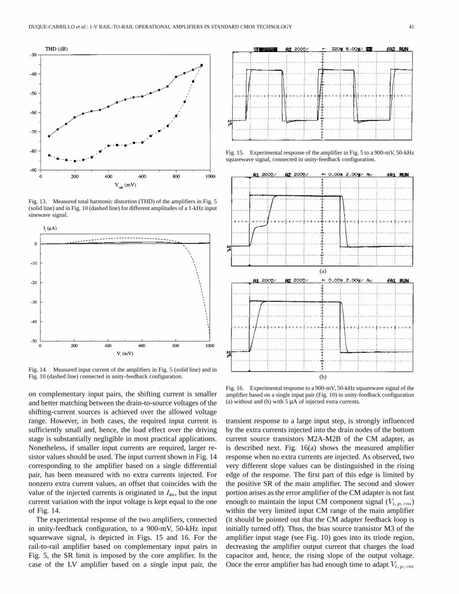
The experimental response of the two amplifiers, connectedin unity-feedback configuration, to a 900-mV, 50-kHz inputsquarewave signal, is depicted in Figs. 15 and 16. For therail-to-rail amplifier based on complementary input pairs inFig. 5, the SR limit is imposed by the core amplifier. In thecase of the LV amplifier based on a single input pair, the
Fig. 15. Experimental response of the amplifier in Fig. 5 to a 900-mV, 50-kHzsquarewave signal, connected in unity-feedback configuration.
(a)
(b)
Fig. 16. Experimental response to a 900-mV, 50-kHz squarewave signal of theamplifier based on a single input pair (Fig. 10) in unity-feedback configuration(a) without and (b) with 5µA of injected extra currents.
transient response to a large input step, is strongly influencedby the extra currents injected into the drain nodes of the bottomcurrent source transistors M2A-M2B of the CM adapter, asis described next. Fig. 16(a) shows the measured amplifierresponse when no extra currents are injected. As observed, twovery different slope values can be distinguished in the risingedge of the response. The first part of this edge is limited bythe positive SR of the main amplifier. The second and slowerportion arises as the error amplifier of the CM adapter is not fastenough to maintain the input CM component signal ( )within the very limited input CM range of the main amplifier(it should be pointed out that the CM adapter feedback loop isinitially turned off). Thus, the bias source transistor M3 of theamplifier input stage (see Fig. 10) goes into its triode region,decreasing the amplifier output current that charges the loadcapacitor and, hence, the rising slope of the output voltage.Once the error amplifier has had enough time to adapt

42 IEEE JOURNAL OF SOLID-STATE CIRCUITS, VOL. 35, NO. 1, JANUARY 2000
Fig. 17. Experimental response of the amplifier in Fig. 5 in switched-bufferconfiguration to a 900-mV , 2-kHz input sinewave (clock frequency = 40 kHz).
Fig. 18. Measured response of the amplifier in Fig. 10 in inverting unity-gainconfiguration to 900-mV , 15-kHz input sinewave.
to the main amplifier CM range, the proper amplifier operationis recovered and, again, the output voltage slope is determinedby the amplifier positive SR. There are two possible ways toavoid this behavior. One of them consists in designing theerror amplifier with higher SR. However, this implies largerbias current values and a smaller compensation capacitancevalue in the circuit in Fig. 9. According to (8), both theseactions adversely affect the loop stability. The second and muchmore effective way consists in injecting the extra currents.Now, the CM adapter feedback loop is never turned off and,therefore, its response speed is significantly improved, as is theloop stability, as indicated in Section III. Fig. 16(b) shows theamplifier response for the same input square signal as before,when two extra currents of 5µA are injected.
Finally, Figs. 17 and 18 present results obtained withtwo simple application schemes, one referred to the sam-pled-data and the other to the continuous-time approach. First,a switched-buffer version of the amplifier in Fig. 5, suitablefor switched-opamp applications [20], was integrated. Themeasured response with 40 kHz of clock frequency to aninput sinewave ( 900 mV, 2 kHz), is shownin Fig. 17. On the other hand, the LV amplifier based on asingle differential pair was connected in inverting unity-gainconfiguration, using externally connected input and feedbackresistors of 47 k . Fig. 18 shows the details of the amplifierresponse to a 0.9- , 15-kHz input sinewave. This responsewas obtained with zero extra currents since, as stated above,in inverting applications the input dc level of the CM adapterremains constant regardless of the input signal level.
TABLE IIIEXPERIMENTAL PERFORMANCE OFAMPLIFIERS IN FIGS. 5 AND 10
(V = 1 V, TECHNOLOGY: 1.2-µm CMOS,C = 15 pF)
A summary of the experimental amplifier performances isshown in Table III. When applies, all the parameters were mea-sured for the input CM level at mid-supply. The current con-sumption is larger in the amplifier based on the dynamic-shiftingapproach with respect to the one based on the CM adapter,mainly due to a larger number of mirroring current operationsin the circuit implementation adopted. Also, the dc gain resultslarger in the circuit of Fig. 5, since a true cascode structure hasbeen used for the first stage. In the case of the amplifier in Fig. 5,the worst case of stability (larger unity-gain bandwidth) occursfor the input CM level at mid-supply, due to the fact that bothinput pairs are active, while for the amplifier in Fig. 10, thephase margin is roughly constant over the entire voltage range.The THD for both amplifiers was measured in unity-gain feed-back configuration. The total harmonic distortion of the 0.5-,40-kHz input signal was−71.1 dB. As expected, at both frequen-cies THD is smaller for the amplifier in Fig. 10. Noise charac-teristic of both amplifiers is dominated by the flicker compo-nent. To reduce the noise contributions by the common-modecontrol network, the values of the resistorsshould be reduced(thus decreasing the effective noise added by the shifting cur-rent sources), but at the cost of increased power consumption.
V. CONCLUSIONS
This paper has addressed the issue of rail-to-rail operationalamplifiers for very low supply voltage operation in standardCMOS technology. Two design approaches have been de-scribed. The first one is based on an amplifier input stage madeup by complementary differential pairs, and uses the dynamiclevel-shifting technique [5] to extend the amplifiers input range

DUQUE-CARRILLO et al.: 1-V RAIL-TO-RAIL OPERATIONAL AMPLIFIERS IN STANDARD CMOS TECHNOLOGY 43
up to the rails. By contrast, the second approach relies on aninput stage based on a single differential input pair. Rail-to-rail operation is achieved thanks to a closed-loop common-mode front-end adapter, which keeps the input common-modevoltage of the pair at an appropriate constant voltage, whileleaving the input signal differential mode unaffected. With thesecond approach, the presence of a single input pair biased ata fixed voltage, ensures that the amplifier offset is maintainedroughly constant over the entire input voltage range, therebyallowing the designer to overcome the typical major limitationof amplifier based on complementary input pairs, i.e., themodest THD figures. Two amplifiers based on the describedapproaches were designed and integrated in standard 1.2-µmCMOS process and were then experimentally evaluated. Mea-sured results showed rail-to-rail operation for both amplifiersat a supply voltage as low as 1 V. As expected, the amplifierbased on the second approach provides better offset and THDperformance. Moreover, in both cases the measured inputcurrent (although smaller for the amplifier based on the firstapproach), is sufficiently small to make the load effect on thepreceding stage negligible in most applications.
REFERENCES
[1] J. H. Huijsing and D. Linebarger, “Low-voltage operational amplifierwith rail-to-rail input and output ranges,”IEEE J. Solid-State Circuits,vol. 20, pp. 1144–1150, Dec. 1985.
[2] S. Sakurai and M. Ismail,Low-Voltage CMOS Operational Amplifiers:Theory, Design, and Implementation. Boston, MA: Kluwer Academic,1995.
[3] R. Hogervost and J. H. Huijsing,Design of Low-Voltage, Low-PowerOperational Amplifier Cells. Boston, MA: Kluwer Academic, 1996.
[4] J. F. Duque-Carrillo, J. M. Valverde, and R . Pérez-Aloe, “Constant-Grail-to-rail common-mode input stage with minimum CMRR degrada-tion,” IEEE J. Solid-State Circuits, vol. 28, pp. 661–667, June 1993.
[5] J. Fonderie, M. M. Maris, E. J. Schnitger, and J. H. Huijsing, “1-V op-erational amplifier with rail-to-rail input and output stages,”IEEE J.Solid-State Circuits, vol. 24, pp. 1551–1559, Dec. 1989.
[6] J. F. Duque-Carrillo, R. Pérez-Aloe, and J. M. Valverde, “Biasing cir-cuit for high input swing operational amplifiers,”IEEE J. Solid-StateCircuits, vol. 30, pp. 156–160, Feb. 1995.
[7] S. Sakurai and M. Ismail, “Robust design of rail-to-rail CMOS opera-tional amplifiers for a low power supply voltage,”IEEE J. Solid-StateCircuits, vol. 31, pp. 146–156, Feb. 1996.
[8] C. Hwang, A. Motamed, and M. Ismail, “Universal constant-g input-stage architectures for low-voltage op amps,”IEEE Trans. Circuits andSystems I (Special Issue on Low-Voltage and Low-Power Analog andMixed-Signal Circuits and Systems), vol. 42, pp. 886–897, Nov. 1995.
[9] R. Hogervost, J. P. Tero, and J. H. Huijsing, “Compact CMOS con-stant-g rail-to-rail input stage withg -control by an electronic zenerdiode,”IEEE J. Solid-State Circuits, vol. 31, pp. 1035–1040, July 1996.
[10] G. Ferri and W. Sansen, “A rail-to-rail constant-g low-voltage CMOSoperational transconductance amplifier,”IEEE J. Solid-State Circuits,vol. 32, pp. 1563–1567, Oct. 1997.
[11] K. Nagaraj, “Constant-transconductance CMOS amplifier input stagewith rail-to-rail input common mode voltage range,”IEEE Trans. Cir-cuits and Systems II, vol. 42, pp. 366–368, May 1995.
[12] J. H. Botma, R. J. Wiegerink, S. L. Gierkink, and R. F. Wassenaar,“Rail-to-rail constant-G input stage and class AB output stage forlow-voltage CMOS op-amps,”Analog Integrated Circuits and SignalProcessing, vol. 6, pp. 121–133, Sept. 1994.
[13] W. Redman-White, “A high bandwidth constant-g and SR rail-to-railCMOS input circuit and its application to analog cells for low voltageVLSI systems,”IEEE J. Solid-State Circuits, vol. 32, pp. 701–712, May1997.
[14] T. A. F. Duisters and E. C. Dijkmans, “A−90 dB THD rail-to-rail inputopamp using a new local charge pump in CMOS,”IEEE J. Solid-StateCircuits, vol. 33, pp. 947–955, July 1998.
[15] B. J. Blalock, P. E. Allen, and G. A. Rincón-Mora, “Designing 1-V opamps using standard digital CMOS technology,”IEEE Trans. Circuitsand Systems II, vol. 45, pp. 769–779, July 1998.
[16] R. Castello, A. G. Grassi, and S. Donati, “A 500-nA sixth-order band-pass SC filter,”IEEE J. Solid-State Circuits, vol. 25, pp. 669–676, June1990.
[17] I. Fujimori and T. Sugimoto, “A 1.5 V, 4.1 mW dual-channel audiodelta-sigma D/A converter,”IEEE J. Solid-State Circuits, vol. 33, pp.1863–1870, Dec. 1998.
[18] P. J. Crawley and G. W. Roberts, “High-swing MOS current mirrors witharbitrarily high output resistance,”Electron. Lett., vol. 28, pp. 361–363,1992.
[19] R. Castello, F. Montecchi, F. Rezzi, and A. Baschirotto, “Low-voltageanalog filters,”IEEE Trans. Circuits and Systems I (Special Issue onLow-Voltage and Low-Power Analog and Mixed-Signal Circuits andSystems), vol. 42, pp. 827–840, Nov. 1995.
[20] J. Crols and M. Steyaert, “Switched-opamp: an approach to realize fullCMOS switched-capacitor circuits at very low power supply voltages,”IEEE J. Solid-State Circuits, vol. 29, pp. 936–942, Aug. 1994.
J. Francisco Duque-Carrillo (M’86) received theM.Sc. degree in electronic physics from the Univer-sity of Sevilla, Spain, and the Ph.D. degree in physicsfrom the University of Extremadura, Badajoz, Spain,in 1979 and 1984, respectively.
In 1986 and 1987, on a NATO Fellowship, hewas a Visiting Scholar at the Electrical EngineeringDepartment of Texas A&M University, College Sta-tion. In 1988, he was with AT&T Microelectronicsin Madrid, Spain, and Allentown, PA. Currently, heis with the University of Extremadura, where he is a
Professor. His research interest focuses on the area of analog and mixed-signalintegrated circuit design.
José L. Ausínwas born in Laredo, Cantabria, Spain,on May 4, 1969. He received the B.Sc. degree inelectronic physics from the University of Cantabria,Cantabria, Spain, in 1993. In 1995, he received aresearch grant from the Spanish R&D Plan. He iscurrently working toward the Ph.D. degree in thefield of low-voltage high-performance sampled datacircuits.
Guido Torelli (M’90–SM’96) was born in Rome,Italy, in 1949. He received the Laurea degree (withhonors) in electronic engineering in 1973 from theUniversity of Pavia, Pavia, Italy.
After graduating, he worked one year in theInstitute of Electronics on a scholarship. In 1974, hejoined SGS ATES (now part of STMicroelectronics),Agrate Brianza (Milan), Italy, where he served asa design engineer for MOS JC’s, and was involvedin both digital and analog circuit development, andwhere he became Head of the MOS IC’s Design
Group for Consumer Applications. In 1987, he joined the Department ofElectronics of the University of Pavia as an Associate Professor. His researchinterests are in the area of MOS integrated circuit design. At present he ismainly concerned with the fields of CMOS analog and mixed analog/digitalcircuits and nonvolatile memories.
Prof. Torelli was a corecipient of the Inst. Electr. Eng. Ambrose Fleming Pre-mium (session 1994–1995). He is a member of the Italian Association of Elec-trical and Electronics Engineers (AEI).

44 IEEE JOURNAL OF SOLID-STATE CIRCUITS, VOL. 35, NO. 1, JANUARY 2000
José M. Valverde was born in Mérida, Badajoz,Spain. He finished his studies in Electronics at theUniversity of Extremadura, Badajoz, Spain.
From 1989 to 1995 he held a Researcher positionin the Department of Electronics at the Universityof Extremadura. Since 1995, he has been a TeacherAssistant at the same university His research interestfocus on instrumentation, IC design for biomedicalapplications, and image and neural information pro-cessing.
Miguel A. Domínguez was born in Sevilla, Spain,on December 13, 1973. He received the B.Sc. andM.Sc. degrees from the University of Extremadura, in1996 and 1998, respectively. He is currently workingtoward the Ph.D. degree in electronics engineering.His research interest is on adaptive filters and mixed-signal circuit design for consumer applications.