Low-Voltage Current Feedback Operational Amplifiers
12
Circuits Syst Signal Process DOI 10.1007/s00034-008-9088-x Low-Voltage Current Feedback Operational Amplifiers George Raikos · Costas Psychalinos Received: 26 September 2007 / Revised: 28 May 2008 © Birkhäuser Boston 2008 Abstract A number of current feedback operational amplifier topologies suitable for operation in a low-voltage environment are introduced in this paper. Their realiza- tion is based on the corresponding low-voltage second generation current conveyor topologies. Important performance factors such as accuracy, bandwidth, and linear- ity have been considered, and the obtained simulation results have been compared in order to evaluate the behavior of the proposed topologies. Keywords Low-voltage circuits · Current feedback operational amplifiers · Analog integrated circuits 1 Introduction The current feedback operational amplifier (CFOA) is one of the most useful elements for realizing various transfer functions required for the implementation of analog sig- nal processing systems. Due to the fact that it is constructed from voltage and current followers, its terminal properties provide significant design flexibility compared to that offered by conventional operational amplifier (op-amp) configurations. In addi- tion, the achieved bandwidth is higher than that achieved by employing op-amps as active elements [9, 12]. Today’s market requirements for low-voltage/low-power portable electronics and communication systems could be fulfilled by employing active building blocks that are capable of operating in an environment where a supply voltage less than or equal G. Raikos · C. Psychalinos ( ) Physics Department, Electronics Laboratory, University of Patras, 26504, Rio, Patras, Greece e-mail: [email protected] G. Raikos e-mail: [email protected]
Transcript of Low-Voltage Current Feedback Operational Amplifiers

Circuits Syst Signal ProcessDOI 10.1007/s00034-008-9088-x
Low-Voltage Current Feedback Operational Amplifiers
George Raikos · Costas Psychalinos
Received: 26 September 2007 / Revised: 28 May 2008© Birkhäuser Boston 2008
Abstract A number of current feedback operational amplifier topologies suitable foroperation in a low-voltage environment are introduced in this paper. Their realiza-tion is based on the corresponding low-voltage second generation current conveyortopologies. Important performance factors such as accuracy, bandwidth, and linear-ity have been considered, and the obtained simulation results have been compared inorder to evaluate the behavior of the proposed topologies.
Keywords Low-voltage circuits · Current feedback operational amplifiers · Analogintegrated circuits
1 Introduction
The current feedback operational amplifier (CFOA) is one of the most useful elementsfor realizing various transfer functions required for the implementation of analog sig-nal processing systems. Due to the fact that it is constructed from voltage and currentfollowers, its terminal properties provide significant design flexibility compared tothat offered by conventional operational amplifier (op-amp) configurations. In addi-tion, the achieved bandwidth is higher than that achieved by employing op-amps asactive elements [9, 12].
Today’s market requirements for low-voltage/low-power portable electronics andcommunication systems could be fulfilled by employing active building blocks thatare capable of operating in an environment where a supply voltage less than or equal
G. Raikos · C. Psychalinos (�)Physics Department, Electronics Laboratory, University of Patras, 26504, Rio, Patras, Greecee-mail: [email protected]
G. Raikose-mail: [email protected]

Circuits Syst Signal Process
to 1.5 V is available. For this purpose, much research effort has been expended todevelop low-voltage active elements.
Several CMOS CFOAs topologies have been introduced in [4–7, 10]. The min-imum supply voltage requirement for the topologies in [4–6] and [10] is equal toVT + 2VDS,sat, where VT is the threshold voltage and VDS,sat is the drain-sourcesaturation voltage of a MOS transistor. In [7] the corresponding value is equal toVT + 3VDS,sat.
In order for the CFOAs to be compatible with today’s industry trends concerningthe power supply voltage, some low-voltage CFOA topologies are introduced in thispaper. They are derived by enhancing the corresponding low-voltage second genera-tion current conveyors (CCIIs), which have already been introduced in the literature[2, 3, 8], in order to establish the well-known properties of the CFOA terminals. Thevoltage conveyance in [2, 3, 8] is achieved by employing appropriately configureddifferential pairs, while the current conveyance is performed by using suitable currentmirrors. These designs have also been followed in the introduced CFOA topologies.The main attractive characteristic of the derived CFOAs is that the minimum supplyvoltage requirement is equal to VT + 2VDS,sat.
The paper is organized as follows. The introduced topologies are discussed inSect. 2. A comparison of their behavior is provided in Sect. 3, where the obtainedresults are also further discussed. The most attractive CFOA topology has been cho-sen for realizing a third-order lowpass filter function by following the well-knownleapfrog method. This has been done in Sect. 4, where both the linear and non-linearperformances of the realized filter have been evaluated through simulation results.
2 Low-Voltage CFOA Topologies
A low-voltage CFOA can be constructed by employing the CCII introduced in [3] andan additional voltage follower. The derived topology is demonstrated in Fig. 1, wherethe voltage conveyance between nodes Y , X and Z, O is established by ensuringthat the same current is fed to the input transistors Mn1–Mn2 and Mn3–Mn4 of thecorresponding differential pairs. This is achieved by the employed current mirrorsformed by transistors Mp1–Mp2 and Mp3–Mp4, respectively. The low impedance atnodes X, O is achieved by employing feedback paths formed by transistors Mp5 andMp7, respectively.
In an alternative view, the voltage conveyance between the corresponding termi-nals of the CFOA in Fig. 1 can be viewed as follows: transistors Mn1–Mn2, Mn6–Mn7, Mp1–Mp2, and Mp5 form a two-stage voltage amplifier whose output terminalis connected to its inverting input terminal. A similar case occurs for the voltageconveyance between nodes Z and O .
The required current conveyance between nodes X, Z is achieved by the matchedMOS transistor pair Mp5–Mp6.
The impedance at node Y is infinite, while the impedances at node X can beexpressed, neglecting second-order terms [1], as
RX = gds,Mn1 + gds,Mp1
gm,Mn1 · gm,Mp5, (1)

Circuits Syst Signal Process
Fig. 1 Low-voltage CFOA based on CCII in [3]
Fig. 2 Low-voltage CFOA based on CCII in [8]
while at node O
RO = gds,Mn3 + gds,Mp3
gm,Mn3 · gm,Mp7. (2)
The impedance at node Z is given by
RZ = 1
gds,Mn8 + gds,Mp6. (3)
The small-signal voltage conveyed between nodes Y , X and Z, O is equal to 1.The operation of the low-voltage CFOA given in Fig. 2 [8] is similar to that in
Fig. 1. The required voltage conveyed between the Y , X and Z, O terminals of theCFOA is established by forcing equal currents to the input transistors of the corre-

Circuits Syst Signal Process
Fig. 3 Low-voltage CFOA based on CCII in [2]
sponding differential pairs (Mn1–Mn2 and Mn3–Mn4, respectively). The low im-pedance at nodes X, O is realized through the diode connected transistors Mn2 andMn4, respectively.
In an alternative view, the voltage conveyed between nodes Y and X is achieved byconnecting the output terminal of the two-stage amplifier constructed from transistorsMn1–Mn2, Mn7, Mp2, and Mp5 to its inverting input terminal. A similar case occursfor the voltage conveyed between nodes Z and O .
The current conveyance is established by employing matched MOS transistor pairsformed by transistors Mp5 and Mp6.
The small-signal input impedances at nodes X and Y are given by (4)–(5):
RX = gds,Mn1 + 2gds,Mp2
(gm,Mn1 + gds,Mn1) · (gm,Mp5 + gds,Mp2), (4)
RO = gds,Mn3 + 2gds,Mp4
(gm,Mn3 + gds,Mn3) · (gm,Mp7 + gds,Mp4), (5)
while the impedance at node Z is still given by (3).The voltages conveyed between nodes Y , X and Z, O are given by (6) and (7),
respectively:
υX
υY
= gm,Mn1
gm,Mn1 + gds,Mn1, (6)
υO
υZ
= gm,Mn3
gm,Mn3 + gds,Mn3. (7)
Another low-voltage CFOA is that shown in Fig. 3 [2]. The voltage conveyed betweenterminals Y , X and Z, O is established by forcing equal currents to the input tran-sistors of the corresponding composite differential pairs (Mn1–Mn2 and Mn3–Mn4,respectively).
In an alternative view, the output terminal of the differential amplifier constructedfrom transistors Mn1, Mn6, Mn11, and Mp1 is connected to its inverting input. As aresult, Mn12 is fed by a voltage equal to that of terminal Y . By simply connecting the

Circuits Syst Signal Process
output of the differential amplifier, constructed from transistors Mn12, Mn2, Mn7,and Mp2–Mp3, to its inverting input, one achieves equal voltages between terminalsY and X. A similar case occurs for the voltage conveyed between nodes Z and O .
The current conveyance is performed by the matched MOS transistor pairsMp3–Mp4.
The small-signal characteristics of the CFOA in Fig. 3 are described by (8)–(12):
RX = gds,Mn11 + gds,Mp1
2gm,Mn1(gm,Mn1 + gds,Mn11 + gds,Mp1), (8)
RO = gds,Mn13 + gds,Mp5
2gm,Mn3(gm,Mn3 + gds,Mn13 + gds,Mp5), (9)
RZ = 1
gds,Mn8 + gds,Mp4, (10)
υX
υY
= 1
1 + gds,Mn11+gds,Mp1gm,Mn1
, (11)
υO
υZ
= 1
1 + gds,Mn13+gds,Mp5gm,Mn3
. (12)
Comparing the corresponding expressions for the X, Z, and O terminals’ resis-tance, it can be concluded that the expressions for RZ are of the same form. Thisoriginates from the fact that current iZ is obtained by subtracting the currents IO + iXand IO that feed the corresponding output transistors. The derived expressions for re-sistances at nodes X and O are different among the considered CFOAs due to thedifferent architectures of the amplifier stages employed for achieving the requiredvoltage conveyance.
A simple inspection of Figs. 1–3 easily shows that, in order to maintain the NMOStransistors in saturation, the minimum voltage requirement at terminals Y , X, and O
should be VT +VDS,sat. This is taken into account in the next section, where the intro-duced CFOAs will be appropriately configured in order to evaluate their performance.
3 Performance Study of the CFOA Topologies
The introduced topologies in Figs. 1–3 have been compared in terms of the most im-portant performance factors in order to evaluate their characteristics. For this purpose,a single power supply voltage VDD = 1.5 V and a dc bias current IO = 50 µA havebeen employed. Note also that Level-49 MOS transistor models of the 0.35 µm AMSS35D4 CMOS process have been employed in simulations through the SpectreS en-vironment of Cadence.
The MOS transistors with aspect ratios denoted as (×2) are constructed for twounit MOS transistors in parallel connection. In order to achieve a fair comparison,the aspect ratios of the unity MOS transistors have been chosen to be equal. Thus, thevalues are 24 µm/1 µm and 70 µm/1 µm for NMOS and PMOS transistors, respec-tively.

Circuits Syst Signal Process
Fig. 4 Configuration of CFOAfor comparison purposes
Table 1 Comparison results for the CFOAs in Figs. 1–3
Performance factor CFOA
Fig. 1 Fig. 2 Fig. 3
RX 25.4 � 39.4 � 113.4 �
RY ∞ ∞ ∞RZ 192.5 k� 183.6 k� 84.9 k�
RO 25.4 � 39.4 � 113.4 �
υX/υY 0.9948 1.018 0.956
υO/υZ 0.9948 1.027 0.961
iZ/iX 1 1.073 1.074
Offset voltage terminal X 85.8 µV 6.9 mV 5.1 mV
Offset current at terminal Z 17.2 nA 4.6 µA 6.3 µA
Offset voltage at terminal O 171.2 µV 30.5 mV 35.4 mV
Range of υY for υY = υX (V) 0.75–1.23 0.82–1.20 0.75–1.19
Range of iX for iZ = iX (µA) −50–60 −25.8–52 −16.3–50
Range of υZ for υO = υZ (V) 0.75–1.23 0.84–1.20 0.75–1.16
Bandwidth (υX/υY ) (MHz) 264.7 134.6 70.4
Bandwidth (υO/υZ) (MHz) 335.3 291.1 104.1
Bandwidth (iZ/iX) (MHz) 806.8 149.9 140.8
THD of υX @ 200 mV 0.6% 4.4% 2.4%
THD of υO @ 200 mV 1.1% 10% 21.5%
THD of iZ @ 200 mV 0.6% 8.8% 15.8%
dc power dissipation (µW) 552 544 756
The testing setup is shown in Fig. 4, where the resistors R have the same value of5 k�. According to the discussion in Sect. 2, the voltage applied at the terminal Y isconstructed from a dc component and a sinusoidal component. A reasonable choiceis VB = 1 V. The configuration in Fig. 4 also guarantees that at the quiescent pointthe following condition will also hold in the ideal case: iX = iZ = 0.
The derived comparison results concerning the most important performance fac-tors of the introduced CFOAs are summarized in Table 1. From this table it can bereadily seen that the CFOA topology in Fig. 1 has the best performance among theCFOAs under comparison with regard to all the considered factors.

Circuits Syst Signal Process
4 Filter Design Example
The passive prototype filter given in Fig. 5 will be used as the prototype filter for real-izing a third-order lowpass filter function. Assuming that the cutoff frequency of thefilter will be equal to fc = 1 MHz, the corresponding element values are summarizedin Table 2.
Following the well-known leapfrog method [11], the derived signal flow graph(SFG), assuming that RS = RL = R, is depicted in Fig. 6. The scaling factors K1
and K2 in the branches of the SFG are defined as K1 = υout,max/υ1,max and K2 =υout,max/(i2R)max and they will be used in order to optimize the dynamic range ofthe filter.
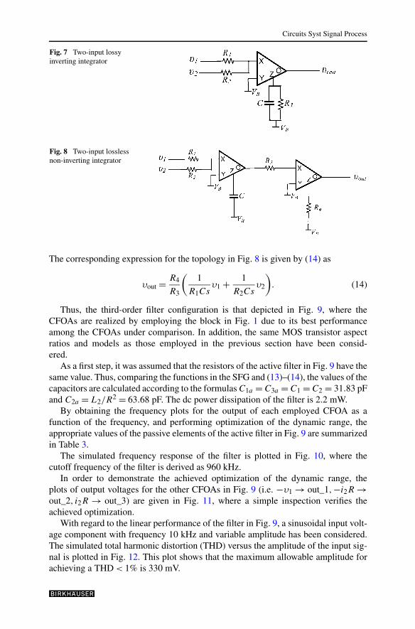
The lossy and lossless integrator blocks that are required for realizing the SFG inFig. 6 are given in Figs. 7 and 8, respectively.
The input–output voltage expression for the topology in Fig. 7 is given in (13) as
υout = − 1
R3Cs + 1
(R3
R1υ1 + R3
R2υ2
). (13)
Fig. 5 Third-order lowpassfilter prototype
Fig. 6 SFG of the filter in Fig. 5
Table 2 Element values for thepassive filter in Fig. 5 Element Value
RS 5 k�
RL 5 k�
C1 31.83 pF
L2 1.59 mH
C3 31.83 pF
Circuits Syst Signal Process
Fig. 7 Two-input lossyinverting integrator
Fig. 8 Two-input losslessnon-inverting integrator
The corresponding expression for the topology in Fig. 8 is given by (14) as
υout = R4
R3
(1
R1Csυ1 + 1
R2Csυ2
). (14)
Thus, the third-order filter configuration is that depicted in Fig. 9, where theCFOAs are realized by employing the block in Fig. 1 due to its best performanceamong the CFOAs under comparison. In addition, the same MOS transistor aspectratios and models as those employed in the previous section have been consid-ered.
As a first step, it was assumed that the resistors of the active filter in Fig. 9 have thesame value. Thus, comparing the functions in the SFG and (13)–(14), the values of thecapacitors are calculated according to the formulas C1a = C3a = C1 = C2 = 31.83 pFand C2a = L2/R
2 = 63.68 pF. The dc power dissipation of the filter is 2.2 mW.By obtaining the frequency plots for the output of each employed CFOA as a
function of the frequency, and performing optimization of the dynamic range, theappropriate values of the passive elements of the active filter in Fig. 9 are summarizedin Table 3.
The simulated frequency response of the filter is plotted in Fig. 10, where thecutoff frequency of the filter is derived as 960 kHz.
In order to demonstrate the achieved optimization of the dynamic range, theplots of output voltages for the other CFOAs in Fig. 9 (i.e. −υ1 → out_1,−i2R →out_2, i2R → out_3) are given in Fig. 11, where a simple inspection verifies theachieved optimization.
With regard to the linear performance of the filter in Fig. 9, a sinusoidal input volt-age component with frequency 10 kHz and variable amplitude has been considered.The simulated total harmonic distortion (THD) versus the amplitude of the input sig-nal is plotted in Fig. 12. This plot shows that the maximum allowable amplitude forachieving a THD < 1% is 330 mV.

Circuits Syst Signal Process
Fig. 9 Third-order lowpass filter with CFOAs
Table 3 Element values for theactive filter in Fig. 9 Element Value
R1 8.3 k�
R2 6.9 k�
R3 5 k�
R4 3.7 k�
R5 6.2 k�
R6 4.0 k�
R7 4.2 k�
R8 4.2 k�
R9 5.0 k�
C1a 31.83 pF
C2a 63.68 pF
C3a 31.83 pF

Circuits Syst Signal Process
Fig. 10 Simulated frequency response of the filter in Fig. 9
Fig. 11 Simulated plots of the output voltages of CFOAs in Fig. 9 as a function of the frequency
The noise has been integrated over a 1.5 MHz range, and the rms value of theoutput voltage noise has been calculated to be equal to 68 µV. Thus, the predicteddynamic range (DR) of the filter will be about 64.7 dB.

Circuits Syst Signal Process
Fig. 12 Linear performance ofthe filter in Fig. 9
5 Conclusions
The introduced CMOS CFOA topologies are capable of operating in a low-voltageenvironment. Comparison of the results and the study of the behavior of a third-order filter show that one of the introduced CFOAs could be employed for realizinghigh-performance analog signal processing systems. Further research could be per-formed to derive other CFOA topologies that offer compatibility with today’s industryneeds.
References
1. W.S. Hassanein, I.A. Awad, A.M. Soliman, Long tail pair based positive CMOS current conveyors:a review. Frequenz 59, 186–194 (2005)
2. A.M. Ismail, A.M. Soliman, Wideband CMOS current conveyor. Electron. Lett. 34, 2368–2369(1998)
3. S. Liu, H. Tsao, J. Wu, CCII based continuous-time filters with reduced gain-bandwidth sensitivity.IEE Proc. G 138, 210–216 (1991)
4. S.A. Mahmoud, H.O. Elwan, A.M. Soliman, Low voltage rail to rail CMOS current feedback op-erational amplifier and its applications for analog VLSI. Analog Integr. Circuits Signal Process. 25,45–57 (2000)
5. S.A. Mahmoud, I.A. Awad, Fully differential CMOS current feedback operational amplifier. AnalogIntegr. Circuits Signal Process. 43, 61–69 (2005)
6. B.J. Maudy, A.S. Sarkar, S.J. Gift, A new design topology for low-voltage CMOS current feedbackamplifiers. IEEE Trans. Circuits Syst. II 53, 34–38 (2006)
7. R. Mita, G. Palumbo, S. Pennisi, Low-voltage high-drive CMOS current feedback op-amp. IEEETrans. Circuits Syst. II 52, 317–321 (2005)
8. G. Palmisiano, G. Palumbo, A simple CMOS CCII+. Int. J. Circuit Theory Appl. 23, 599–603 (1995)9. A. Payne, C. Toumazou, Analog amplifiers: classification and generalization. IEEE Trans. Circuits
Syst. I 43, 43–50 (1996)

Circuits Syst Signal Process
10. S. Pennisi, High-performance CMOS current feedback operational amplifier, in Proc. IEEE Int. Symp.on Circ. and Syst. (ISCAS), II, Kobe, Japan, pp. 1573–1576 (2005)
11. A.S. Sedra, P.O. Brackett, Filter Theory and Design: Active and Passive (Matrix Publishers, Portland,1978)
12. A.M. Soliman, Applications of the current feedback operational amplifiers. Analog Integr. CircuitsSignal Process. 11, 265–302 (1996)