Operational Amplifiers - Solayman EWU
72
CHAPTER 2 Operational Amplifiers Introduction 53 2.1 The Ideal Op Amp 54 2.2 The Inverting Configuration 58 2.3 The Noninverting Configuration 67 2.4 Difference Amplifiers 71 2.5 Integrators and Differentiators 80 2.6 DC Imperfections 88 2.7 Effect of Finite Open-Loop Gain and Bandwidth on Circuit Performance 97 2.8 Large-Signal Operation of Op Amps 102 Summary 107 Problems 108
-
Upload
khangminh22 -
Category
Documents
-
view
0 -
download
0
Transcript of Operational Amplifiers - Solayman EWU

CHAPTER 2
Operational Amplifiers
Introduction 53
2.1 The Ideal Op Amp 54
2.2 The Inverting Configuration 58
2.3 The Noninverting Configuration 67
2.4 Difference Amplifiers 71
2.5 Integrators and Differentiators 80
2.6 DC Imperfections 88
2.7 Effect of Finite Open-Loop Gain and Bandwidth on Circuit Performance 97
2.8 Large-Signal Operation of Op Amps 102
Summary 107
Problems 108

53
IN THIS CHAPTER YOU WILL LEARN
1. The terminal characteristics of the ideal op amp.
2. How to analyze circuits containing op amps, resistors, and capacitors.
3. How to use op amps to design amplifiers having precise characteristics.
4. How to design more sophisticated op-amp circuits, including summingamplifiers, instrumentation amplifiers, integrators, and differentiators.
5. Important nonideal characteristics of op amps and how these limit theperformance of basic op-amp circuits.
Introduction
Having learned basic amplifier concepts and terminology, we are now ready to undertake thestudy of a circuit building block of universal importance: The operational amplifier (op amp).Op amps have been in use for a long time, their initial applications being primarily in the areasof analog computation and sophisticated instrumentation. Early op amps were constructedfrom discrete components (vacuum tubes and then transistors, and resistors), and their cost wasprohibitively high (tens of dollars). In the mid-1960s the first integrated-circuit (IC) op ampwas produced. This unit (the μA 709) was made up of a relatively large number of transistorsand resistors all on the same silicon chip. Although its characteristics were poor (by today’sstandards) and its price was still quite high, its appearance signaled a new era in electronic cir-cuit design. Electronics engineers started using op amps in large quantities, which caused theirprice to drop dramatically. They also demanded better-quality op amps. Semiconductor manu-facturers responded quickly, and within the span of a few years, high-quality op amps becameavailable at extremely low prices (tens of cents) from a large number of suppliers.
One of the reasons for the popularity of the op amp is its versatility. As we will shortlysee, one can do almost anything with op amps! Equally important is the fact that the IC opamp has characteristics that closely approach the assumed ideal. This implies that it is quiteeasy to design circuits using the IC op amp. Also, op-amp circuits work at performance levelsthat are quite close to those predicted theoretically. It is for this reason that we are studying opamps at this early stage. It is expected that by the end of this chapter the reader should be ableto design nontrivial circuits successfully using op amps.
As already implied, an IC op amp is made up of a large number (tens or more) of tran-sistors, resistors, and (usually) one capacitor connected in a rather complex circuit. Since

54 Chapter 2 Operational Amplifiers
we have not yet studied transistor circuits, the circuit inside the op amp will not be dis-cussed in this chapter. Rather, we will treat the op amp as a circuit building block and studyits terminal characteristics and its applications. This approach is quite satisfactory in manyop-amp applications. Nevertheless, for the more difficult and demanding applications it isquite useful to know what is inside the op-amp package. This topic will be studied in Chap-ter 12. More advanced applications of op amps will appear in later chapters.
2.1 The Ideal Op Amp
2.1.1 The Op-Amp Terminals
From a signal point of view the op amp has three terminals: two input terminals and one outputterminal. Figure 2.1 shows the symbol we shall use to represent the op amp. Terminals 1 and 2are input terminals, and terminal 3 is the output terminal. As explained in Section 1.4, amplifiersrequire dc power to operate. Most IC op amps require two dc power supplies, as shown inFig. 2.2. Two terminals, 4 and 5, are brought out of the op-amp package and connected to a pos-itive voltage VCC and a negative voltage −VEE, respectively. In Fig. 2.2(b) we explicitly show thetwo dc power supplies as batteries with a common ground. It is interesting to note that the refer-ence grounding point in op-amp circuits is just the common terminal of the two power supplies;that is, no terminal of the op-amp package is physically connected to ground. In what followswe will not, for simplicity, explicitly show the op-amp power supplies.
Figure 2.2 The op amp shown connected to dc power supplies.
Figure 2.1 Circuit symbol for the op amp.
VCC
�VEE
VCC
VEE

2.1 The Ideal Op Amp 55
In addition to the three signal terminals and the two power-supply terminals, an op ampmay have other terminals for specific purposes. These other terminals can include terminalsfor frequency compensation and terminals for offset nulling; both functions will be explainedin later sections.
2.1.2 Function and Characteristics of the Ideal Op Amp
We now consider the circuit function of the op amp. The op amp is designed to sense the dif-ference between the voltage signals applied at its two input terminals (i.e., the quantity v2 −v1), multiply this by a number A, and cause the resulting voltage A(v2 − v1) to appear at out-put terminal 3. Thus v3 = A(v2 − v1). Here it should be emphasized that when we talk aboutthe voltage at a terminal we mean the voltage between that terminal and ground; thus v1means the voltage applied between terminal 1 and ground.
The ideal op amp is not supposed to draw any input current; that is, the signal currentinto terminal 1 and the signal current into terminal 2 are both zero. In other words, the inputimpedance of an ideal op amp is supposed to be infinite.
How about the output terminal 3? This terminal is supposed to act as the output termi-nal of an ideal voltage source. That is, the voltage between terminal 3 and ground willalways be equal to A(v2 − v1), independent of the current that may be drawn from terminal 3into a load impedance. In other words, the output impedance of an ideal op amp is supposedto be zero.
Putting together all of the above, we arrive at the equivalent circuit model shown inFig. 2.3. Note that the output is in phase with (has the same sign as) v2 and is out of phasewith (has the opposite sign of) v1. For this reason, input terminal 1 is called the invertinginput terminal and is distinguished by a “−” sign, while input terminal 2 is called the nonin-verting input terminal and is distinguished by a “+” sign.
As can be seen from the above description, the op amp responds only to the differencesignal v2 − v1 and hence ignores any signal common to both inputs. That is, if v1 = v2 = 1 V,then the output will (ideally) be zero. We call this property common-mode rejection, and weconclude that an ideal op amp has zero common-mode gain or, equivalently, infinite com-mon-mode rejection. We will have more to say about this point later. For the time beingnote that the op amp is a differential-input, single-ended-output amplifier, with the lat-ter term referring to the fact that the output appears between terminal 3 and ground.1
1Some op amps are designed to have differential outputs. This topic will not be discussed in this book. Rather, we confine ourselves here to single-ended-output op amps, which constitute the vast majority of commercially available op amps.
2.1 What is the minimum number of terminals required by a single op amp? What is the minimumnumber of terminals required on an integrated-circuit package containing four op amps (called aquad op amp)?Ans. 5; 14
EXERCISE

56 Chapter 2 Operational Amplifiers
Furthermore, gain A is called the differential gain, for obvious reasons. Perhaps not so obvi-ous is another name that we will attach to A: the open-loop gain. The reason for this namewill become obvious later on when we “close the loop” around the op amp and define anothergain, the closed-loop gain.
An important characteristic of op amps is that they are direct-coupled or dc amplifiers,where dc stands for direct-coupled (it could equally well stand for direct current, since adirect-coupled amplifier is one that amplifies signals whose frequency is as low as zero). Thefact that op amps are direct-coupled devices will allow us to use them in many importantapplications. Unfortunately, though, the direct-coupling property can cause some seriouspractical problems, as will be discussed in a later section.
How about bandwidth? The ideal op amp has a gain A that remains constant down tozero frequency and up to infinite frequency. That is, ideal op amps will amplify signals of anyfrequency with equal gain, and are thus said to have infinite bandwidth.
We have discussed all of the properties of the ideal op amp except for one, which infact is the most important. This has to do with the value of A. The ideal op amp should havea gain A whose value is very large and ideally infinite. One may justifiably ask: If the gain Ais infinite, how are we going to use the op amp? The answer is very simple: In almost allapplications the op amp will not be used alone in a so-called open-loop configuration.Rather, we will use other components to apply feedback to close the loop around the opamp, as will be illustrated in detail in Section 2.2.
For future reference, Table 2.1 lists the characteristics of the ideal op amp.
Figure 2.3 Equivalent circuit of the ideal op amp.
Table 2.1 Characteristics of the Ideal Op Amp
1. Infinite input impedance2. Zero output impedance3. Zero common-mode gain or, equivalently, infinite common-mode rejection4. Infinite open-loop gain A5. Infinite bandwidth
Inverting input
Noninverting input
Output

2.1 The Ideal Op Amp 57
2.1.3 Differential and Common-Mode Signals
The differential input signal vId is simply the difference between the two input signalsv1 and v2; that is,
(2.1)
The common-mode input signal vIcm is the average of the two input signals v1 and v2;namely,
(2.2)
Equations (2.1) and (2.2) can be used to express the input signals v1 and v2 in terms of theirdifferential and common-mode components as follows:
(2.3)
and
(2.4)
These equations can in turn lead to the pictorial representation in Fig. 2.4.
Figure 2.4 Representation of the signal sources v1 and v2 in terms of their differential and common-mode components.
vId v2 v1–=
vIcm12--- v1 v2+( )=
v1 vIcm vId 2⁄–=
v2 vIcm vId 2⁄+=
��v1
1
��v2
2
�� vId�2
��
1
2
��vIcm vId�2
2.2 Consider an op amp that is ideal except that its open-loop gain A = 103. The op amp is used in a feed-back circuit, and the voltages appearing at two of its three signal terminals are measured. In each ofthe following cases, use the measured values to find the expected value of the voltage at the third ter-minal. Also give the differential and common-mode input signals in each case. (a) v2 = 0 V and v3 =2 V; (b) v2 = +5 V and v3 = −10 V; (c) v1 = 1.002 V and v2 = 0.998 V; (d) v1 = −3.6 V and v3 = −3.6 V.Ans. (a) v1 = −0.002 V, vId = 2 mV, vIcm = −1 mV; (b) v1 = +5.01 V, vId = −10 mV, vIcm = 5.005 � 5 V;(c) v3 = −4 V, vId = −4 mV, vIcm = 1 V; (d) v2 = −3.6036 V, vId = −3.6 mV, vIcm � −3.6 V
EXERCISES

58 Chapter 2 Operational Amplifiers
2.2 The Inverting Configuration
As mentioned above, op amps are not used alone; rather, the op amp is connected to passivecomponents in a feedback circuit. There are two such basic circuit configurations employingan op amp and two resistors: the inverting configuration, which is studied in this section, andthe noninverting configuration, which we shall study in the next section.
Figure 2.5 shows the inverting configuration. It consists of one op amp and two resistors R1and R2. Resistor R2 is connected from the output terminal of the op amp, terminal 3, back to theinverting or negative input terminal, terminal 1. We speak of R2 as applying negative feedback;if R2 were connected between terminals 3 and 2 we would have called this positive feedback.Note also that R2 closes the loop around the op amp. In addition to adding R2, we have groundedterminal 2 and connected a resistor R1 between terminal 1 and an input signal source with a volt-age vI. The output of the overall circuit is taken at terminal 3 (i.e., between terminal 3 and
2.3 The internal circuit of a particular op amp can be modeled by the circuit shown in Fig. E2.3. Expressv3 as a function of v1 and v2. For the case Gm = 10 mA/V, R = 10 kΩ, and μ = 100, find the value ofthe open-loop gain A.Ans. v3 = μGmR(v2 − v1); A = 10,000 V/V or 80 dB
Figure E2.3

2.2 The Inverting Configuration 59
ground). Terminal 3 is, of course, a convenient point from which to take the output, since theimpedance level there is ideally zero. Thus the voltage vO will not depend on the value of the cur-rent that might be supplied to a load impedance connected between terminal 3 and ground.
2.2.1 The Closed-Loop Gain
We now wish to analyze the circuit in Fig. 2.5 to determine the closed-loop gain G, defined as
We will do so assuming the op amp to be ideal. Figure 2.6(a) shows the equivalent circuit,and the analysis proceeds as follows: The gain A is very large (ideally infinite). If we assumethat the circuit is “working” and producing a finite output voltage at terminal 3, then thevoltage between the op-amp input terminals should be negligibly small and ideally zero.Specifically, if we call the output voltage vO, then, by definition,
It follows that the voltage at the inverting input terminal (v1) is given by v1 = v2. That is,because the gain A approaches infinity, the voltage v1 approaches and ideally equals v2. Wespeak of this as the two input terminals “tracking each other in potential.” We also speak of a“virtual short circuit” that exists between the two input terminals. Here the word virtual shouldbe emphasized, and one should not make the mistake of physically shorting terminals 1 and 2together while analyzing a circuit. A virtual short circuit means that whatever voltage is at 2will automatically appear at 1 because of the infinite gain A. But terminal 2 happens to be con-nected to ground; thus v2 = 0 and v1 = 0. We speak of terminal 1 as being a virtual ground—that is, having zero voltage but not physically connected to ground.
Now that we have determined v1 we are in a position to apply Ohm’s law and find thecurrent i1 through R1 (see Fig. 2.6) as follows:
Where will this current go? It cannot go into the op amp, since the ideal op amp has an infiniteinput impedance and hence draws zero current. It follows that i1 will have to flow through R2 tothe low-impedance terminal 3. We can then apply Ohm’s law to R2 and determine vO; that is,
Thus,
Figure 2.5 The inverting closed-loopconfiguration.
GvO
vI-----≡
v2 v1–vO
A----- 0= =
i1vI v1–
R1--------------- vI 0–
R1------------- vI
R1-----= = =
vO v1 i1R2–=
0=vI
R1-----R2–
vO
vI----- R2
R1-----–=

60 Chapter 2 Operational Amplifiers
which is the required closed-loop gain. Figure 2.6(b) illustrates these steps and indicates bythe circled numbers the order in which the analysis is performed.
We thus see that the closed-loop gain is simply the ratio of the two resistances R2 and R1.The minus sign means that the closed-loop amplifier provides signal inversion. Thus if
and we apply at the input (vI ) a sine-wave signal of 1 V peak-to-peak, then theoutput vO will be a sine wave of 10 V peak-to-peak and phase-shifted 180° with respect to theinput sine wave. Because of the minus sign associated with the closed-loop gain, this config-uration is called the inverting configuration.
Figure 2.6 Analysis of the inverting configuration. The circled numbers indicate the order of the analysis steps.
5
6
4
1
3
2
�
�
R2 R1⁄ = 10
2.2 The Inverting Configuration 61
The fact that the closed-loop gain depends entirely on external passive components(resistors R1 and R2) is very significant. It means that we can make the closed-loop gain asaccurate as we want by selecting passive components of appropriate accuracy. It alsomeans that the closed-loop gain is (ideally) independent of the op-amp gain. This is a dra-matic illustration of negative feedback: We started out with an amplifier having very largegain A, and through applying negative feedback we have obtained a closed-loop gain
that is much smaller than A but is stable and predictable. That is, we are trading gainfor accuracy.
2.2.2 Effect of Finite Open-Loop Gain
The points just made are more clearly illustrated by deriving an expression for the closed-loop gain under the assumption that the op-amp open-loop gain A is finite. Figure 2.7 showsthe analysis. If we denote the output voltage vO, then the voltage between the two inputterminals of the op amp will be Since the positive input terminal is grounded, thevoltage at the negative input terminal must be The current i1 through R1 can now befound from
The infinite input impedance of the op amp forces the current i1 to flow entirely throughR2. The output voltage vO can thus be determined from
Collecting terms, the closed-loop gain G is found as
(2.5)
We note that as A approaches ∞, G approaches the ideal value of Also, from Fig. 2.7we see that as A approaches ∞, the voltage at the inverting input terminal approaches zero.This is the virtual-ground assumption we used in our earlier analysis when the op amp was
R2 R1⁄
vO A.⁄vO A.⁄–
i1vI vO A⁄–( )–
R1------------------------------- vI vO A⁄+
R1------------------------= =
Figure 2.7 Analysis of the invertingconfiguration taking into account the finiteopen-loop gain of the op amp.
vOvO
A-----– i1R2–=
vO
A----- –=
vI vO A⁄+R1
------------------------⎝ ⎠⎛ ⎞– R2
GvO
vI-----≡
R2 R1⁄–1 1 R2 R1⁄+( ) A⁄+----------------------------------------------=
R– 2 R1⁄ .

62 Chapter 2 Operational Amplifiers
assumed to be ideal. Finally, note that Eq. (2.5) in fact indicates that to minimizethe dependence of the closed-loop gain G on the value of the open-loop gain A, we shouldmake
2.2.3 Input and Output Resistances
Assuming an ideal op amp with infinite open-loop gain, the input resistance of the closed-loopinverting amplifier of Fig. 2.5 is simply equal to R1. This can be seen from Fig. 2.6(b), where
Now recall that in Section 1.5 we learned that the amplifier input resistance forms a voltagedivider with the resistance of the source that feeds the amplifier. Thus, to avoid the loss of signalstrength, voltage amplifiers are required to have high input resistance. In the case of the invert-ing op-amp configuration we are studying, to make Ri high we should select a high value for R1.However, if the required gain is also high, then R2 could become impractically large(e.g., greater than a few megohms). We may conclude that the inverting configuration suffersfrom a low input resistance. A solution to this problem is discussed in Example 2.2 below.
1R2
R1----- � A+
Consider the inverting configuration with R1 = 1 kΩ and R2 = 100 kΩ.
(a) Find the closed-loop gain for the cases A = 103, 104, and 105. In each case determine the percentageerror in the magnitude of G relative to the ideal value of (obtained with A = ∞). Also deter-mine the voltage v1 that appears at the inverting input terminal when vI = 0.1 V.
(b) If the open-loop gain A changes from 100,000 to 50,000 (i.e., drops by 50%), what is the correspond-ing percentage change in the magnitude of the closed-loop gain G?
Solution
(a) Substituting the given values in Eq. (2.5), we obtain the values given in the following table, where thepercentage error ε is defined as
The values of v1 are obtained from with vI = 0.1 V.
(b) Using Eq. (2.5), we find that for A = 50,000, |G| = 99.80. Thus a −50% change in the open-loop gainresults in a change of only −0.1% in the closed-loop gain!
A |G| ε v1
103 90.83 −9.17% −9.08 mV104 99.00 −1.00% −0.99 mV105 99.90 −0.10% −0.10 mV
R2 R1⁄
εG R2 R1⁄( )–
R2 R1⁄( )---------------------------------- 100×≡
v1 = vO A⁄– GvI A⁄=
Example 2.1
RivI
i1----≡
vI
vI R1⁄-------------- R1= =
R2 R1⁄

2.2 The Inverting Configuration 63
Since the output of the inverting configuration is taken at the terminals of the ideal voltagesource A(v2 − v1) (see Fig. 2.6a), it follows that the output resistance of the closed-loop ampli-fier is zero.
Assuming the op amp to be ideal, derive an expression for the closed-loop gain of the circuitshown in Fig. 2.8. Use this circuit to design an inverting amplifier with a gain of 100 and an inputresistance of 1 MΩ. Assume that for practical reasons it is required not to use resistors greater than1 MΩ. Compare your design with that based on the inverting configuration of Fig. 2.5.
Figure 2.8 Circuit for Example 2.2. The circled numbers indicate the sequence of the steps in the analysis.
vO vI⁄
4
5
7
6
3
1
2
8
vx
x
�
�
Solution
The analysis begins at the inverting input terminal of the op amp, where the voltage is
Here we have assumed that the circuit is “working” and producing a finite output voltage vO. Know-ing v1, we can determine the current i1 as follows:
Since zero current flows into the inverting input terminal, all of i1 will flow through R2, and thus
Now we can determine the voltage at node x:
v1vO–
A---------
vO–
∞--------- 0= = =
i1vI v1–
R1---------------
vI 0–
R1-------------
vI
R1-----= = =
i2 i1vI
R1-----= =
vx v1 i2R2– 0 vI
R1-----– R2
R2
R1-----vI–= = =
Example 2.2
64 Chapter 2 Operational Amplifiers
Example 2.2 continued
This in turn enables us to find the current i3:
Next, a node equation at x yields i4:
Finally, we can determine vO from
Thus the voltage gain is given by
which can be written in the form
Now, since an input resistance of 1 MΩ is required, we select R1 = 1 MΩ. Then, with the limita-tion of using resistors no greater than 1 MΩ, the maximum value possible for the first factor in thegain expression is 1 and is obtained by selecting R2 = 1 MΩ. To obtain a gain of −100, R3 and R4must be selected so that the second factor in the gain expression is 100. If we select the maximumallowed (in this example) value of 1 MΩ for R4, then the required value of R3 can be calculated tobe 10.2 kΩ. Thus this circuit utilizes three 1-MΩ resistors and a 10.2-kΩ resistor. In comparison,if the inverting configuration were used with R1 = 1 MΩ we would have required a feedback resis-tor of 100 MΩ, an impractically large value!
Before leaving this example it is insightful to inquire into the mechanism by which the circuit isable to realize a large voltage gain without using large resistances in the feedback path. Toward thatend, observe that because of the virtual ground at the inverting input terminal of the op amp, R2 and R3are in effect in parallel. Thus, by making R3 lower than R2 by, say, a factor k (i.e., where k > 1), R3 isforced to carry a current k-times that in R2. Thus, while i2 = i1, i3 = ki1 and i4 = (k + 1)i1. It is the currentmultiplication by a factor of (k + 1) that enables a large voltage drop to develop across R4 and hence alarge vO without using a large value for R4. Notice also that the current through R4 is independent of thevalue of R4. It follows that the circuit can be used as a current amplifier as shown in Fig. 2.9.
i30 vx–
R3-------------
R2
R1R3------------vI= =
i4 i2 i3+vI
R1-----
R2
R1R3------------vI+= =
vO vx i4R4–=R2
R1-----– vI=
vI
R1-----
R2
R1R3------------vI+⎝ ⎠
⎛ ⎞R4–
vO
vI------ R2
R1-----
R4
R1----- 1
R2
R3------+⎝ ⎠
⎛ ⎞+–=
vO
vI------
R2
R1----- 1
R4
R2-----
R4
R3-----+ +⎝ ⎠
⎛ ⎞–=
iI
R2
R3
R4
�
�
v1 � 0
i2 � iI i4
R2
R3i3 � iI
R2
R3i4 � �1 � �iI
Figure 2.9 A current amplifier based on thecircuit of Fig. 2.8. The amplifier delivers itsoutput current to R4. It has a current gain of(1 + R2/R3), a zero input resistance, and an infi-nite output resistance. The load (R4), however,must be floating (i.e., neither of its two termi-nals can be connected to ground).
2.2 The Inverting Configuration 65
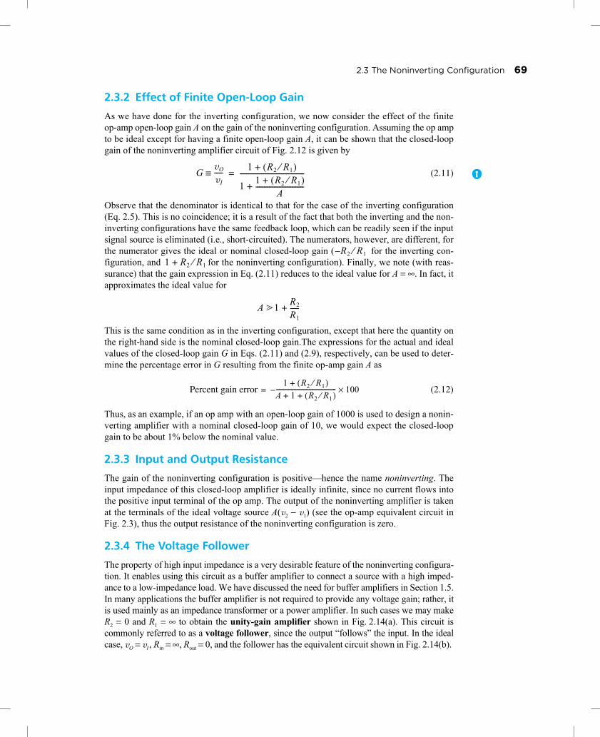
2.2.4 An Important Application—The Weighted Summer
A very important application of the inverting configuration is the weighted-summer cir-cuit shown in Fig. 2.10. Here we have a resistance Rf in the negative-feedback path (asbefore); but we have a number of input signals v1, v2, . . . , vn each applied to a corre-sponding resistor R1, R2, . . . , Rn, which are connected to the inverting terminal of the opamp. From our previous discussion, the ideal op amp will have a virtual ground appearing
D2.4 Use the circuit of Fig. 2.5 to design an inverting amplifier having a gain of −10 and an input resist-ance of 100 kΩ. Give the values of R1 and R2.Ans. R1 = 100 kΩ; R2 = 1 MΩ
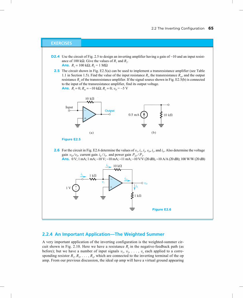
2.5 The circuit shown in Fig. E2.5(a) can be used to implement a transresistance amplifier (see Table1.1 in Section 1.5). Find the value of the input resistance Ri, the transresistance Rm, and the outputresistance Ro of the transresistance amplifier. If the signal source shown in Fig. E2.5(b) is connectedto the input of the transresistance amplifier, find its output voltage.Ans. Ri = 0; Rm = −10 kΩ; Ro = 0; vO = −5 V
Figure E2.5
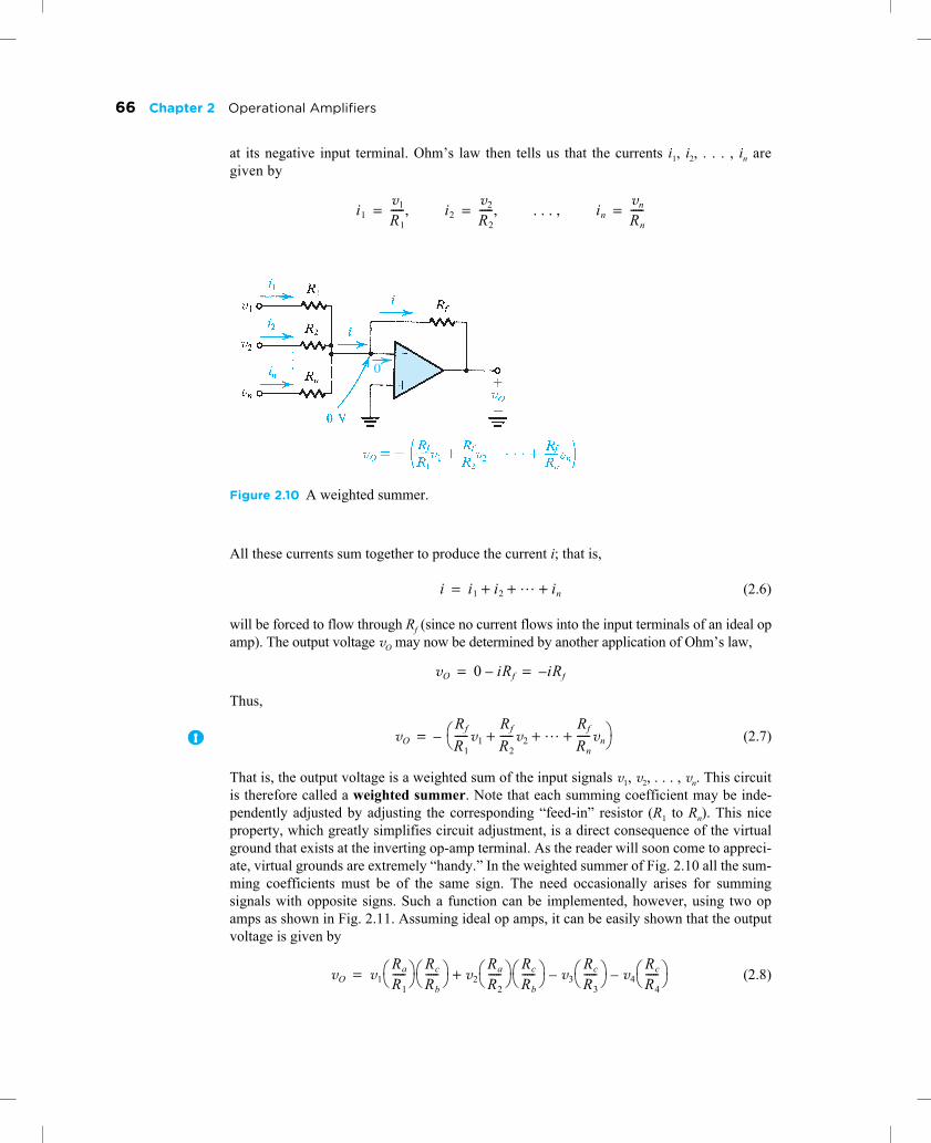
2.6 For the circuit in Fig. E2.6 determine the values of v1, i1, i2, vO, iL, and iO. Also determine the voltagegain current gain and power gain Ans. 0 V; 1 mA; 1 mA; −10 V; −10 mA; −11 mA; −10 V/V (20 dB), −10 A/A (20 dB); 100 W/W (20 dB)
vO vI⁄ , iL iI⁄ , PO PI⁄ .
iL
v1 vO
10 k�
1 k�
1 k�
i2
iO
i1
�
���1 V
Figure E2.6
EXERCISES
66 Chapter 2 Operational Amplifiers
at its negative input terminal. Ohm’s law then tells us that the currents i1, i2, . . . , in aregiven by
All these currents sum together to produce the current i; that is,
(2.6)
will be forced to flow through Rf (since no current flows into the input terminals of an ideal opamp). The output voltage vO may now be determined by another application of Ohm’s law,
Thus,
(2.7)
That is, the output voltage is a weighted sum of the input signals v1, v2, . . . , vn. This circuitis therefore called a weighted summer. Note that each summing coefficient may be inde-pendently adjusted by adjusting the corresponding “feed-in” resistor (R1 to Rn). This niceproperty, which greatly simplifies circuit adjustment, is a direct consequence of the virtualground that exists at the inverting op-amp terminal. As the reader will soon come to appreci-ate, virtual grounds are extremely “handy.” In the weighted summer of Fig. 2.10 all the sum-ming coefficients must be of the same sign. The need occasionally arises for summingsignals with opposite signs. Such a function can be implemented, however, using two opamps as shown in Fig. 2.11. Assuming ideal op amps, it can be easily shown that the outputvoltage is given by
(2.8)
Figure 2.10 A weighted summer.
i1v1
R1----- i2,
v2
R2----- . . . in, ,
vn
Rn-----= = =
0
i i1 i2… in+ + +=
vO 0 iRf– iRf–= =
vO Rf
R1-----v1
Rf
R2-----v2
… Rf
Rn-----vn+ + +⎝ ⎠
⎛ ⎞–=
vO v1Ra
R1-----⎝ ⎠
⎛ ⎞ Rc
Rb-----⎝ ⎠
⎛ ⎞ v2Ra
R2-----⎝ ⎠
⎛ ⎞ Rc
Rb-----⎝ ⎠
⎛ ⎞ v3Rc
R3-----⎝ ⎠
⎛ ⎞– v4Rc
R4-----⎝ ⎠
⎛ ⎞–+=

2.3 The Noninverting Configuration 67
2.3 The Noninverting Configuration
The second closed-loop configuration we shall study is shown in Fig. 2.12. Here the inputsignal vI is applied directly to the positive input terminal of the op amp while one terminal ofR1 is connected to ground.
2.3.1 The Closed-Loop Gain
Analysis of the noninverting circuit to determine its closed-loop gain is illustratedin Fig. 2.13. Again the order of the steps in the analysis is indicated by circled numbers.Assuming that the op amp is ideal with infinite gain, a virtual short circuit exists between itstwo input terminals. Hence the difference input signal is
Thus the voltage at the inverting input terminal will be equal to that at the noninverting inputterminal, which is the applied voltage vI. The current through R1 can then be determined as
. Because of the infinite input impedance of the op amp, this current will flow throughR2, as shown in Fig. 2.13. Now the output voltage can be determined from
Figure 2.11 A weighted summer capable of implementing summing coefficients of both signs.
v1
Ra
R1Rb�
�v2
R2
v3
vOR3
v4
R4
Rc
�
�
vO vI⁄( )
vIdvO
A----- 0 for A ∞= = =
vI R1⁄
vO vIvI
R1-----⎝ ⎠
⎛ ⎞R2+=
D2.7 Design an inverting op-amp circuit to form the weighted sum vO of two inputs v1 and v2. It isrequired that vO = − (v1 + 5v2). Choose values for R1, R2, and Rf so that for a maximum output volt-age of 10 V the current in the feedback resistor will not exceed 1 mA.Ans. A possible choice: R1 = 10 kΩ, R2 = 2 kΩ, and Rf = 10 kΩ
D2.8 Use the idea presented in Fig. 2.11 to design a weighted summer that provides
Ans. A possible choice: R1 = 5 kΩ , R2 = 10 kΩ , Ra = 10 kΩ , Rb = 10 kΩ , R3 = 2.5 kΩ,Rc = 10 kΩ.
vO 2v1 v2 4v3–+=
EXERCISES

68 Chapter 2 Operational Amplifiers
which yields
(2.9)
Further insight into the operation of the noninverting configuration can be obtained byconsidering the following: Since the current into the op-amp inverting input is zero, the cir-cuit composed of R1 and R2 acts in effect as a voltage divider feeding a fraction of the outputvoltage back to the inverting input terminal of the op amp; that is,
(2.10)
Then the infinite op-amp gain and the resulting virtual short circuit between the two input termi-nals of the op amp forces this voltage to be equal to that applied at the positive input terminal; thus,
which yields the gain expression given in Eq. (2.9).This is an appropriate point to reflect further on the action of the negative feedback present
in the noninverting circuit of Fig. 2.12. Let vI increase. Such a change in vI will cause vId toincrease, and vO will correspondingly increase as a result of the high (ideally infinite) gain of theop amp. However, a fraction of the increase in vO will be fed back to the inverting input terminalof the op amp through the (R1, R2) voltage divider. The result of this feedback will be to counter-act the increase in vId , driving vId back to zero, albeit at a higher value of vO that corresponds tothe increased value of vI . This degenerative action of negative feedback gives it the alternativename degenerative feedback. Finally, note that the argument above applies equally well if vIdecreases. A formal and detailed study of feedback is presented in Chapter 10.
Figure 2.13 Analysis of the noninverting circuit. The sequence of the steps in the analysis is indicated by the circled numbers.
Figure 2.12 The noninverting configuration.
vO � vI �
�
�
R2
R1
vId � 0 V
vI
vO
R2 � vI R1R1
vI
R1
vI
vI�
��
�
vI
�
�
1 �
R2
R1
0
3
5
2
1 4
6
vO
vI----- 1
R2
R1-----+=
v1 vOR1
R1 R2+-----------------⎝ ⎠
⎛ ⎞=
vOR1
R1 R2+-----------------⎝ ⎠
⎛ ⎞ vI=
2.3 The Noninverting Configuration 69
2.3.2 Effect of Finite Open-Loop Gain
As we have done for the inverting configuration, we now consider the effect of the finiteop-amp open-loop gain A on the gain of the noninverting configuration. Assuming the op ampto be ideal except for having a finite open-loop gain A, it can be shown that the closed-loopgain of the noninverting amplifier circuit of Fig. 2.12 is given by
(2.11)
Observe that the denominator is identical to that for the case of the inverting configuration(Eq. 2.5). This is no coincidence; it is a result of the fact that both the inverting and the non-inverting configurations have the same feedback loop, which can be readily seen if the inputsignal source is eliminated (i.e., short-circuited). The numerators, however, are different, forthe numerator gives the ideal or nominal closed-loop gain ( for the inverting con-figuration, and for the noninverting configuration). Finally, we note (with reas-surance) that the gain expression in Eq. (2.11) reduces to the ideal value for A = ∞. In fact, itapproximates the ideal value for
This is the same condition as in the inverting configuration, except that here the quantity onthe right-hand side is the nominal closed-loop gain.The expressions for the actual and idealvalues of the closed-loop gain G in Eqs. (2.11) and (2.9), respectively, can be used to deter-mine the percentage error in G resulting from the finite op-amp gain A as
Percent gain error (2.12)
Thus, as an example, if an op amp with an open-loop gain of 1000 is used to design a nonin-verting amplifier with a nominal closed-loop gain of 10, we would expect the closed-loopgain to be about 1% below the nominal value.
2.3.3 Input and Output Resistance
The gain of the noninverting configuration is positive—hence the name noninverting. Theinput impedance of this closed-loop amplifier is ideally infinite, since no current flows intothe positive input terminal of the op amp. The output of the noninverting amplifier is takenat the terminals of the ideal voltage source A(v2 − v1) (see the op-amp equivalent circuit inFig. 2.3), thus the output resistance of the noninverting configuration is zero.
2.3.4 The Voltage Follower
The property of high input impedance is a very desirable feature of the noninverting configura-tion. It enables using this circuit as a buffer amplifier to connect a source with a high imped-ance to a low-impedance load. We have discussed the need for buffer amplifiers in Section 1.5.In many applications the buffer amplifier is not required to provide any voltage gain; rather, itis used mainly as an impedance transformer or a power amplifier. In such cases we may makeR2 = 0 and R1 = ∞ to obtain the unity-gain amplifier shown in Fig. 2.14(a). This circuit iscommonly referred to as a voltage follower, since the output “follows” the input. In the idealcase, vO = vI , Rin = ∞, Rout = 0, and the follower has the equivalent circuit shown in Fig. 2.14(b).
GvO
vI-----≡ 1 R2 R1⁄( )+
1 1 R2 R1⁄( )+A
-----------------------------+---------------------------------------=
R2 R1⁄–1 R2 R1⁄+
A 1> R2
R1-----+>>
1 R2 R1⁄( )+
A 1 R2 R1⁄( )+ +---------------------------------------- 100×–=

70 Chapter 2 Operational Amplifiers
Since in the voltage-follower circuit the entire output is fed back to the inverting input,the circuit is said to have 100% negative feedback. The infinite gain of the op amp then actsto make vId = 0 and hence vO = vI. Observe that the circuit is elegant in its simplicity!
Since the noninverting configuration has a gain greater than or equal to unity, dependingon the choice of , some prefer to call it “a follower with gain.”
Figure 2.14 (a) The unity-gain buffer or follower amplifier. (b) Its equivalent circuit model.
vO � vIvI
�
�
�
�
��
(a)
�
�
1 � vI��vI
�
�
vO
(b )
R2 R1⁄
2.9 Use the superposition principle to find the output voltage of the circuit shown in Fig. E2.9.Ans. vO = 6v1 + 4v2
2.10 If in the circuit of Fig. E2.9 the 1-kΩ resistor is disconnected from ground and connected to a thirdsignal source v3, use superposition to determine vO in terms of v1, v2, and v3.Ans. vO = 6v1 + 4v2 − 9v3
D2.11 Design a noninverting amplifier with a gain of 2. At the maximum output voltage of 10 V the cur-rent in the voltage divider is to be 10 μA.Ans. R1 = R2 = 0.5 MΩ
2.12 (a) Show that if the op amp in the circuit of Fig. 2.12 has a finite open-loop gain A, then the closed-loop gain is given by Eq. (2.11). (b) For R1 = 1 kΩ and R2 = 9 kΩ find the percentage deviation εof the closed-loop gain from the ideal value of for the cases A = 103, 104, and 105.For vI = 1 V, find in each case the voltage between the two input terminals of the op amp.Ans. ε = −1%, − 0.1%, − 0.01%; v2 − v1 = 9.9 mV, 1 mV, 0.1 mV
Figure E2.9
1 R2 R1⁄+( )
EXERCISES

2.4 Difference Amplifiers 71
2.4 Difference AmplifiersHaving studied the two basic configurations of op-amp circuits together with some of theirdirect applications, we are now ready to consider a somewhat more involved but veryimportant application. Specifically, we shall study the use of op amps to design difference ordifferential amplifiers.2 A difference amplifier is one that responds to the difference betweenthe two signals applied at its input and ideally rejects signals that are common to the twoinputs. The representation of signals in terms of their differential and common-mode com-ponents was given in Fig. 2.4. It is repeated here in Fig. 2.15 with slightly different symbolsto serve as the input signals for the difference amplifiers we are about to design. Althoughideally the difference amplifier will amplify only the differential input signal vId and rejectcompletely the common-mode input signal vIcm, practical circuits will have an output voltagevO given by
(2.13)
where Ad denotes the amplifier differential gain and Acm denotes its common-mode gain (ide-ally zero). The efficacy of a differential amplifier is measured by the degree of its rejectionof common-mode signals in preference to differential signals. This is usually quantified by ameasure known as the common-mode rejection ratio (CMRR), defined as
(2.14)
2The terms difference and differential are usually used to describe somewhat different amplifier types. For our purposes at this point, the distinction is not sufficiently significant. We will be more precise near the end of this section.
vO AdvId AcmvIcm+=
CMRR 20 logAd
Acm------------=
2.13 For the circuit in Fig. E2.13 find the values of iI, v1, i1, i2, vO, iL, and iO. Also find the voltage gain the current gain and the power gain
Ans. 0; 1 V; 1 mA; 1 mA; 10 V; 10 mA; 11 mA; 10 V/V (20 dB); ∞; ∞
2.14 It is required to connect a transducer having an open-circuit voltage of 1 V and a source resistanceof 1 MΩ to a load of 1-kΩ resistance. Find the load voltage if the connection is done (a) directly and(b) through a unity-gain voltage follower.Ans. (a) 1 mV; (b) 1 V
vO vI,⁄ iL iI⁄ , PL PI⁄ .
iL
v1 vO
9 k�
1 k�
1 k�
i2
i1iO
iI
�
�
��vI � 1 V
Figure E2.13

72 Chapter 2 Operational Amplifiers
The need for difference amplifiers arises frequently in the design of electronic systems, espe-cially those employed in instrumentation. As a common example, consider a transducer pro-viding a small (e.g., 1 mV) signal between its two output terminals while each of the twowires leading from the transducer terminals to the measuring instrument may have a largeinterference signal (e.g., 1 V) relative to the circuit ground. The instrument front end obvi-ously needs a difference amplifier.
Before we proceed any further we should address a question that the reader might have:The op amp is itself a difference amplifier; why not just use an op amp? The answer is thatthe very high (ideally infinite) gain of the op amp makes it impossible to use by itself. Rather,as we did before, we have to devise an appropriate feedback network to connect to the opamp to create a circuit whose closed-loop gain is finite, predictable, and stable.
2.4.1 A Single-Op-Amp Difference Amplifier
Our first attempt at designing a difference amplifier is motivated by the observation that thegain of the noninverting amplifier configuration is positive, while that of theinverting configuration is negative, . Combining the two configurations together isthen a step in the right direction⎯namely, getting the difference between two input signals.Of course, we have to make the two gain magnitudes equal in order to reject common-modesignals. This, however, can be easily achieved by attenuating the positive input signal toreduce the gain of the positive path from to . The resulting circuitwould then look like that shown in Fig. 2.16, where the attenuation in the positive input pathis achieved by the voltage divider (R3, R4). The proper ratio of this voltage divider can bedetermined from
which can be put in the form
This condition is satisfied by selecting
(2.15)
vIcm vId�2
vId�2
vId � vI2 � vI1
vIcm � (vI1 � vI2)
vI1 � vIcm � vId�2
vI2 � vIcm � vId�2
12
��
��
��
Figure 2.15 Representing the input signals to adifferential amplifier in terms of their differentialand common-mode components.
1 R2 R1⁄+( ),R2 R1⁄–( )
1 R2 R1⁄+( ) R2 R1⁄( )
R4
R4 R3+----------------- 1
R2
R1-----+⎝ ⎠
⎛ ⎞ R2
R1-----=
R4
R4 R3+----------------- R2
R2 R1+-----------------=
R4
R3----- R2
R1-----=

2.4 Difference Amplifiers 73
This completes our work. However, we have perhaps proceeded a little too fast! Let’s stepback and verify that the circuit in Fig. 2.16 with R3 and R4 selected according to Eq. (2.15)does in fact function as a difference amplifier. Specifically, we wish to determine the outputvoltage vO in terms of vI1 and vI 2. Toward that end, we observe that the circuit is linear, andthus we can use superposition.
To apply superposition, we first reduce vI 2 to zero⎯that is, ground the terminal towhich vI2 is applied⎯and then find the corresponding output voltage, which will be dueentirely to vI1. We denote this output voltage vO1. Its value may be found from the circuit inFig. 2.17(a), which we recognize as that of the inverting configuration. The existence of R3and R4 does not affect the gain expression, since no current flows through either of them.Thus,
Next, we reduce vI1 to zero and evaluate the corresponding output voltage vO2. The circuitwill now take the form shown in Fig. 2.17(b), which we recognize as the noninverting con-figuration with an additional voltage divider, made up of R3 and R4, connected to the inputvI2. The output voltage vO2 is therefore given by
where we have utilized Eq. (2.15).The superposition principle tells us that the output voltage vO is equal to the sum of vO1
and vO2. Thus we have
(2.16)
Thus, as expected, the circuit acts as a difference amplifier with a differential gain Ad of
(2.17)
Of course this is predicated on the op amp being ideal and furthermore on the selection of R3and R4 so that their ratio matches that of R1 and R2 (Eq. 2.15). To make this matchingrequirement a little easier to satisfy, we usually select
vI1
vI2
Figure 2.16 A difference amplifier.
vO1R2
R1-----vI1–=
vO2 vI2R4
R3 R4+----------------- 1
R2
R1-----+⎝ ⎠
⎛ ⎞ R2
R1-----vI2= =
vOR2
R1----- vI2 vI1–( )
R2
R1-----vId==
AdR2
R1-----=

74 Chapter 2 Operational Amplifiers
Let’s next consider the circuit with only a common-mode signal applied at the input, asshown in Fig. 2.18. The figure also shows some of the analysis steps. Thus,
(2.18)
The output voltage can now be found from
Substituting i2 = i1 and for i1 from Eq. (2.18),
Thus,
(2.19)
For the design with the resistor ratios selected according to Eq. (2.15), we obtain
as expected. Note, however, that any mismatch in the resistance ratios can make Acm nonzero,and hence CMRR finite.
In addition to rejecting common-mode signals, a difference amplifier is usually requiredto have a high input resistance. To find the input resistance between the two input terminals
Figure 2.17 Application of superposition to the analysis of the circuit of Fig. 2.16.
vI1
vI2
R3 R1 and R4 R2= =
i11R1----- vIcm
R4
R4 R3+-----------------vIcm–=
vIcmR3
R4 R3+----------------- 1
R1-----=
vOR4
R4 R3+-----------------vIcm i2R2–=
vOR4
R4 R3+-----------------vIcm
R2
R1----- R3
R4 R3+-----------------vIcm–=
R4
R4 R3+----------------- 1
R2
R1-----
R3
R4-----–⎝ ⎠
⎛ ⎞ vIcm=
AcmvO
vIcm--------≡
R4
R4 R3+-----------------⎝ ⎠⎛ ⎞ 1
R2
R1-----
R3
R4-----–⎝ ⎠
⎛ ⎞=
Acm 0=

2.4 Difference Amplifiers 75
(i.e., the resistance seen by vId), called the differential input resistance Rid, consider Fig. 2.19.Here we have assumed that the resistors are selected so that
and
Now
Since the two input terminals of the op amp track each other in potential, we may write aloop equation and obtain
Thus,
(2.20)
Note that if the amplifier is required to have a large differential gain , then R1 ofnecessity will be relatively small and the input resistance will be correspondingly low, adrawback of this circuit. Another drawback of the circuit is that it is not easy to vary the dif-ferential gain of the amplifier. Both of these drawbacks are overcome in the instrumentationamplifier discussed next.
Figure 2.18 Analysis of the difference amplifier to determine its common-mode gain
vO
i1
R2
R4
R1
R3
i2
��
vIcm
vIcm� �R4
R4 � R3
�
�
Acm vO vIcm⁄ .≡
R3 R1= R4 R2=
RidvId
iI------≡
vId R1iI 0 R1iI+ +=
Rid 2R1=
R2 R1⁄( )
vId
Rid
I
I Figure 2.19 Finding the input resis-tance of the difference amplifier forthe case R3 = R1 and R4 = R2.

76 Chapter 2 Operational Amplifiers
2.4.2 A Superior Circuit—The Instrumentation Amplifier
The low-input-resistance problem of the difference amplifier of Fig. 2.16 can be solved by usingvoltage followers to buffer the two input terminals; that is, a voltage follower of the type in Fig. 2.14is connected between each input terminal and the corresponding input terminal of the differenceamplifier. However, if we are going to use two additional op amps, we should ask the question: Canwe get more from them than just impedance buffering? An obvious answer would be that weshould try to get some voltage gain. It is especially interesting that we can achieve this without com-promising the high input resistance simply by using followers with gain rather than unity-gain fol-lowers. Achieving some or indeed the bulk of the required gain in this new first stage of the
(a)
R1
R2
R1
X
vI1
R2
R3
R3
R4
vI21 � � �R2
R1
vI11 � � �R2
R1�
�A1
R4
vI2
�
�
vO
�
�A2
�
�A3
Figure 2.20 A popular circuit for an instrumentation amplifier. (a) Initial approach to the circuit (b) Thecircuit in (a) with the connection between node X and ground removed and the two resistors R1 and R1 lumpedtogether. This simple wiring change dramatically improves performance. (c) Analysis of the circuit in(b) assuming ideal op amps.
2.15 Consider the difference-amplifier circuit of Fig. 2.16 for the case R1 = R3 = 2 kΩ and R2 = R4 =200 kΩ. (a) Find the value of the differential gain Ad. (b) Find the value of the differential inputresistance Rid and the output resistance Ro. (c) If the resistors have 1% tolerance (i.e., each can bewithin ±1% of its nominal value), use Eq. (2.19) to find the worst-case common-mode gain Acm
and hence the corresponding value of CMRR.Ans. (a) 100 V/V (40 dB); (b) 4 kΩ, 0 Ω; (c) 0.04 V/V, 68 dB
D2.16 Find values for the resistances in the circuit of Fig. 2.16 so that the circuit behaves as a differenceamplifier with an input resistance of 20 kΩ and a gain of 10.Ans. R1 = R3 = 10 kΩ; R2 = R4 = 100 kΩ
EXERCISES
2.4 Difference Amplifiers 77
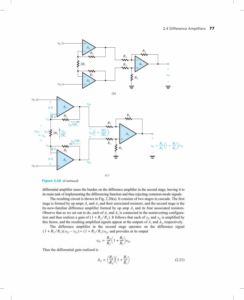
differential amplifier eases the burden on the difference amplifier in the second stage, leaving it toits main task of implementing the differencing function and thus rejecting common-mode signals.
The resulting circuit is shown in Fig. 2.20(a). It consists of two stages in cascade. The firststage is formed by op amps A1 and A2 and their associated resistors, and the second stage is theby-now-familiar difference amplifier formed by op amp A3 and its four associated resistors.Observe that as we set out to do, each of A1 and A2 is connected in the noninverting configura-tion and thus realizes a gain of . It follows that each of vI1 and vI2 is amplified bythis factor, and the resulting amplified signals appear at the outputs of A1 and A2, respectively.
The difference amplifier in the second stage operates on the difference signal= and provides at its output
Thus the differential gain realized is
(2.21)
(b)
vI1
vI2
A1
R2
2R1
A2
R3
R4
A3
�
�
�
�
�
�
�
�
vO
R4
R3
R2
(c )
vI1
vI2
R2
R3
R4
A3
A2
A1
� �
�
�
�
�
vI1
vI2
0
0
�vId/2R1
vId/2R1
R2
�
(vI2 � vI1)� vId 2R1
vId
R3
R4
2R1
0 V
0 V
�
�
�
��
�
vId 2R1
2R21 �
vO1
vO2
�
�
vOR4
R3� vId
R2
R1� 1
Figure 2.20 (Continued)
1 R2 R1⁄+( )
1 R2 R1⁄+( ) vI2 vI1–( ) 1 R2 R1⁄+( )vId
vOR4
R3----- 1
R2
R1-----+⎝ ⎠
⎛ ⎞ vId=
AdR4
R3-----⎝ ⎠⎛ ⎞= 1
R2
R1-----+⎝ ⎠
⎛ ⎞

78 Chapter 2 Operational Amplifiers
The common-mode gain will be zero because of the differencing action of the second-stageamplifier.
The circuit in Fig. 2.20(a) has the advantage of very high (ideally infinite) input resis-tance and high differential gain. Also, provided A1 and A2 and their corresponding resistorsare matched, the two signal paths are symmetric⎯a definite advantage in the design of a dif-ferential amplifier. The circuit, however, has three major disadvantages:
1. The input common-mode signal vIcm is amplified in the first stage by a gain equal tothat experienced by the differential signal vId. This is a very serious issue, for it couldresult in the signals at the outputs of A1 and A3 being of such large magnitudes that theop amps saturate (more on op-amp saturation in Section 2.8). But even if the op ampsdo not saturate, the difference amplifier of the second stage will now have to dealwith much larger common-mode signals, with the result that the CMRR of the overallamplifier will inevitably be reduced.
2. The two amplifier channels in the first stage have to be perfectly matched, otherwisea spurious signal may appear between their two outputs. Such a signal would getamplified by the difference amplifier in the second stage.
3. To vary the differential gain Ad , two resistors have to be varied simultaneously, saythe two resistors labeled R1. At each gain setting the two resistors have to be perfectlymatched: a difficult task.
All three problems can be solved with a very simple wiring change: Simply disconnect thenode between the two resistors labeled R1, node X, from ground. The circuit with this smallbut functionally profound change is redrawn in Fig. 2.20(b), where we have lumped the tworesistors (R1 and R1) together into a single resistor (2R1).
Analysis of the circuit in Fig. 2.20(b), assuming ideal op amps, is straightforward, as isillustrated in Fig. 2.20(c). The key point is that the virtual short circuits at the inputs of opamps A1 and A2 cause the input voltages vI1 and vI2 to appear at the two terminals of resistor(2R1). Thus the differential input voltage vI2 − vI1 ≡ vId appears across 2R1 and causes a current
to flow through 2R1 and the two resistors labeled R2. This current in turn pro-duces a voltage difference between the output terminals of A1 and A2 given by
The difference amplifier formed by op amp A3 and its associated resistors senses the voltagedifference (vO2 − vO1) and provides a proportional output voltage vO :
Thus the overall differential voltage-gain is given by
(2.22)
Observe that proper differential operation does not depend on the matching of the two resistorslabeled R2. Indeed, if one of the two is of different value, say R2′, the expression for Ad becomes
(2.23)
i vId 2R1⁄=
vO2 vO1– 12R2
2R1---------+⎝ ⎠
⎛ ⎞ vId=
vOR4
R3----- vO2 vO1–( )=
R4
R3----- 1
R2
R1------+⎝ ⎠
⎛ ⎞ vId=
AdvO
vId------≡
R4
R3----- 1
R2
R1------+⎝ ⎠
⎛ ⎞=
AdR4
R3-----= 1
R2 R′2+2R1
-------------------+⎝ ⎠⎛ ⎞

2.4 Difference Amplifiers 79
Consider next what happens when the two input terminals are connected together to a common-mode input voltage vIcm. It is easy to see that an equal voltage appears at the negative input terminalsof A1 and A2, causing the current through 2R1 to be zero. Thus there will be no current flowing in theR2 resistors, and the voltages at the output terminals of A1 and A2 will be equal to the input (i.e., vIcm).Thus the first stage no longer amplifies vIcm; it simply propagates vIcm to its two output terminals,where they are subtracted to produce a zero common-mode output by A3. The difference amplifierin the second stage, however, now has a much improved situation at its input: The difference signalhas been amplified by while the common-mode voltage remained unchanged.
Finally, we observe from the expression in Eq. (2.22) that the gain can be varied bychanging only one resistor, 2R1. We conclude that this is an excellent differential amplifiercircuit and is widely employed as an instrumentation amplifier; that is, as the input amplifierused in a variety of electronic instruments.
1 R2 R1⁄+( )
Design the instrumentation amplifier circuit in Fig. 2.20(b) to provide a gain that can be varied overthe range of 2 to 1000 utilizing a 100-kΩ variable resistance (a potentiometer, or “pot” for short).
Solution
It is usually preferable to obtain all the required gain in the first stage, leaving the second stage toperform the task of taking the difference between the outputs of the first stage and thereby rejecting thecommon-mode signal. In other words, the second stage is usually designed for a gain of 1. Adoptingthis approach, we select all the second-stage resistors to be equal to a practically convenient value,say 10 kΩ. The problem then reduces to designing the first stage to realize a gain adjustable over therange of 2 to 1000. Implementing 2R1 as the series combination of a fixed resistor R1f and the vari-able resistor R1v obtained using the 100-kΩ pot (Fig. 2.21), we can write
Thus,
and
These two equations yield R1f = 100.2 Ω and R2 = 50.050 kΩ. Other practical values may beselected; for instance, R1f = 100 Ω and R2 = 49.9 kΩ (both values are available as standard 1%-tolerance metal-film resistors; see Appendix H) results in a gain covering approximately therequired range.
12R2
R1f R1v+---------------------+ 2 to 1000=
12R2
R1f---------+ = 1000
12R2
R1f 100 kΩ+--------------------------------+ 2=
R1v
2R1
R1f
100 k�pot Figure 2.21 To make the gain of the circuit in Fig. 2.20(b) variable, 2R1 is
implemented as the series combination of a fixed resistor R1f and a variableresistor R1v. Resistor R1f ensures that the maximum available gain is limited.
Example 2.3

80 Chapter 2 Operational Amplifiers
2.5 Integrators and Differentiators
The op-amp circuit applications we have studied thus far utilized resistors in the op-ampfeedback path and in connecting the signal source to the circuit, that is, in the feed-in path.As a result, circuit operation has been (ideally) independent of frequency. By allowing theuse of capacitors together with resistors in the feedback and feed-in paths of op-amp cir-cuits, we open the door to a very wide range of useful and exciting applications of the opamp. We begin our study of op-amp–RC circuits by considering two basic applications,namely, signal integrators and differentiators.
2.5.1 The Inverting Configuration with General Impedances
To begin with, consider the inverting closed-loop configuration with impedances Z1(s) andZ2(s) replacing resistors R1 and R2, respectively. The resulting circuit is shown in Fig. 2.22and, for an ideal op amp, has the closed-loop gain or, more appropriately, the closed-looptransfer function
(2.24)
As explained in Section 1.6, replacing s by jω provides the transfer function for physical fre-quencies ω, that is, the transmission magnitude and phase for a sinusoidal input signal offrequency ω.
Figure 2.22 The inverting configuration with general impedances in the feedback and the feed-in paths.
2.17 Consider the instrumentation amplifier of Fig. 2.20(b) with a common-mode input voltage of +5 V(dc) and a differential input signal of 10-mV-peak sine wave. Let (2R1) = 1 kΩ, R2 = 0.5 MΩ, andR3 = R4 = 10 kΩ. Find the voltage at every node in the circuit.Ans. vI1 = 5 − 0.005 sin ω t; vI2 = 5 + 0.005 sin ω t; v– (op amp A1) = 5 − 0.005 sin ω t; v– (op ampA2) = 5 + 0.005 sin ω t; vO1 = 5 − 5.005 sin ωt; vO2 = 5 + 5.005 sin ω t; v– (A3) = v + (A3) = 2.5 + 2.5025sin ω t; vO = 10.01 sin ω t (all in volts)
EXERCISE
Vo s( )Vi s( )------------- −
Z2 s( )Z1 s( )------------=

2.5 Integrators and Differentiators 81
For the circuit in Fig. 2.23, derive an expression for the transfer function Show that thetransfer function is that of a low-pass STC circuit. By expressing the transfer function in the stan-dard form shown in Table 1.2 on page 34, find the dc gain and the 3-dB frequency. Design the circuitto obtain a dc gain of 40 dB, a 3-dB frequency of 1 kHz, and an input resistance of 1 kΩ. At what fre-quency does the magnitude of transmission become unity? What is the phase angle at thisfrequency?
Solution
To obtain the transfer function of the circuit in Fig. 2.23, we substitute in Eq. (2.24), Z1 = R1 and Since Z2 is the parallel connection of two components, it is more convenient to
work in terms of Y2; that is, we use the following alternative form of the transfer function:
and substitute Z1 = R1 and to obtain
This transfer function is of first order, has a finite dc gain and has zerogain at infinite frequency. Thus it is the transfer function of a low-pass STC network and can beexpressed in the standard form of Table 1.2 as follows:
from which we find the dc gain K to be
Vo s( ) Vi s( )⁄ .
Figure 2.23 Circuit for Example 2.4.
Z2 R2|| 1 sC2⁄( ).=
Vo s( )Vi s( )------------- 1
Z1 s( )Y2 s( )--------------------------–=
Y2 s( ) 1 R2⁄( ) sC2+=
Vo s( )Vi s( )------------- 1
R1
R2----- sC2R1+---------------------------–=
at s 0 Vo Vi⁄, R2 R1⁄–= =( ),
Vo s( )Vi s( )-------------
R2 R1⁄–
1 sC2R2+------------------------=
K = R2
R1-----–
Example 2.4

82 Chapter 2 Operational Amplifiers
2.5.2 The Inverting Integrator
By placing a capacitor in the feedback path (i.e., in place of Z2 in Fig. 2.22) and a resistor atthe input (in place of Z1), we obtain the circuit of Fig. 2.24(a). We shall now show that thiscircuit realizes the mathematical operation of integration. Let the input be a time-varyingfunction vI (t). The virtual ground at the inverting op-amp input causes vI (t) to appear ineffect across R, and thus the current i1(t) will be This current flows through thecapacitor C, causing charge to accumulate on C. If we assume that the circuit begins opera-tion at time t = 0, then at an arbitrary time t the current i1(t) will have deposited on C acharge equal to Thus the capacitor voltage vC(t) will change by Ifthe initial voltage on C (at t = 0) is denoted VC , then
Now the output voltage vO(t) = −vC(t); thus,
(2.25)
Thus the circuit provides an output voltage that is proportional to the time integral of theinput, with VC being the initial condition of integration and CR the integrator time constant.Note that, as expected, there is a negative sign attached to the output voltage, and thus this
vI t( ) R.⁄
∫ it0 1 t( ) dt. 1
C----∫ it
0 1 t( ) dt.
vC t( ) VC1C---- i1 t( ) td
0
t
∫+=
vO t( ) 1CR--------– vI t( ) td
0
t
∫ VC–=
Example 2.4 continued
and the 3-dB frequency ω 0 as
We could have found all this from the circuit in Fig. 2.23 by inspection. Specifically, note that thecapacitor behaves as an open circuit at dc; thus at dc the gain is simply Furthermore,because there is a virtual ground at the inverting input terminal, the resistance seen by the capacitoris R2, and thus the time constant of the STC network is C2R2.
Now to obtain a dc gain of 40 dB, that is, 100 V/V, we select For an input resis-tance of 1 kΩ, we select R1 = 1 kΩ, and thus R2 = 100 kΩ. Finally, for a 3-dB frequency f0 = 1 kHz,we select C2 from
which yields C2 = 1.59 nF.The circuit has gain and phase Bode plots of the standard form in Fig. 1.23. As the gain falls off at therate of –20 dB/decade, it will reach 0 dB in two decades, that is, at f = 100f0 = 100 kHz. As Fig.1.23(b) indicates, at such a frequency which is much greater than f0, the phase is approximately −90°.To this, however, we must add the 180° arising from the inverting nature of the amplifier (i.e., thenegative sign in the transfer function expression). Thus at 100 kHz, the total phase shift will be −270°or, equivalently, +90°.
ω0 = 1C2R2------------
R2– R1⁄( ).
R2 R1⁄ = 100.
2π 1 103×× 1C2 100 103××------------------------------------=

2.5 Integrators and Differentiators 83
integrator circuit is said to be an inverting integrator. It is also known as a Miller integra-tor after an early worker in this field.
The operation of the integrator circuit can be described alternatively in the frequencydomain by substituting Z1(s) = R and in Eq. (2.24) to obtain the transferfunction
(2.26)
For physical frequencies, s = jω and
(2.27)
Thus the integrator transfer function has magnitude
(2.28)
Figure 2.24 (a) The Miller or inverting integrator. (b) Frequency response of the integrator.
� vC �
�
�
i1CR 0
Vo
Vi
1sCR
� �
vO(t) � �� vI(t) dt�VC
�
�
i11 t
CR 0
vO(t)vI (t) �
�
(a)
0 V
(b)
Z2 s( ) = 1 sC⁄
Vo s( )Vi s( )------------- 1
sCR----------–=
Vo jω( )Vi jω( )------------------ 1
jωCR--------------–=
Vo
Vi-----
1ωCR------------=

84 Chapter 2 Operational Amplifiers
and phase
(2.29)
The Bode plot for the integrator magnitude response can be obtained by noting from Eq. (2.28)that as ω doubles (increases by an octave) the magnitude is halved (decreased by 6 dB).Thus the Bode plot is a straight line of slope –6 dB/octave (or, equivalently, –20 dB/decade). This line (shown in Fig. 2.24b) intercepts the 0-dB line at the frequency that makes
which from Eq. (2.28) is
(2.30)
The frequency ωint is known as the integrator frequency and is simply the inverse of theintegrator time constant.
Comparison of the frequency response of the integrator to that of an STC low-pass net-work indicates that the integrator behaves as a low-pass filter with a corner frequency of zero.Observe also that at ω = 0, the magnitude of the integrator transfer function is infinite. Thisindicates that at dc the op amp is operating with an open loop. This should also be obviousfrom the integrator circuit itself. Reference to Fig. 2.24(a) shows that the feedback element isa capacitor, and thus at dc, where the capacitor behaves as an open circuit, there is no nega-tive feedback! This is a very significant observation and one that indicates a source of prob-lems with the integrator circuit: Any tiny dc component in the input signal will theoreticallyproduce an infinite output. Of course, no infinite output voltage results in practice; rather, theoutput of the amplifier saturates at a voltage close to the op-amp positive or negativepower supply (L+ or L−), depending on the polarity of the input dc signal.
The dc problem of the integrator circuit can be alleviated by connecting a resistor RFacross the integrator capacitor C, as shown in Fig. 2.25 and thus the gain at dc will be –RF /Rrather than infinite. Such a resistor provides a dc feedback path. Unfortunately, however, theintegration is no longer ideal, and the lower the value of RF, the less ideal the integrator circuitbecomes. This is because RF causes the frequency of the integrator pole to move from its ideallocation at ω = 0 to one determined by the corner frequency of the STC network (RF , C). Spe-cifically, the integrator transfer function becomes
φ +90°=
Vo Vi⁄ = 1,
ωint1
CR--------=
Vo s( )Vi s( )------------- RF R⁄
1 sCRF+----------------------–=
C
�
�vO
�
�
R
RF
(t)�
�
vI (t) Figure 2.25 The Miller integrator with a large resistance RFconnected in parallel with C in order to provide negative feed-back and hence finite gain at dc.

2.5 Integrators and Differentiators 85
as opposed to the ideal function of The lower the value we select for RF , thehigher the corner frequency will be and the more nonideal the integratorbecomes. Thus selecting a value for RF presents the designer with a trade-off between dcperformance and signal performance. The effect of RF on integrator performance is investi-gated further in the Example 2.5.
1 sCR⁄ .–1 CRF⁄( )
Find the output produced by a Miller integrator in response to an input pulse of 1-V height and 1-mswidth [Fig. 2.26(a)]. Let R = 10 kΩ and C = 10 nF. If the integrator capacitor is shunted by a 1-MΩresistor, how will the response be modified? The op amp is specified to saturate at ±13 V.
Solution
In response to a 1-V, 1-ms input pulse, the integrator output will be
where we have assumed that the initial voltage on the integrator capacitor is 0. For C = 10 nF andR = 10 kΩ, CR = 0.1 ms, and
which is the linear ramp shown in Fig. 2.26(b). It reaches a magnitude of −10 V at t = 1 ms andremains constant thereafter.
That the output is a linear ramp should also be obvious from the fact that the 1-V input pulseproduces a constant current through the capacitor of . This constant currentI = 0.1 mA supplies the capacitor with a charge and thus the capacitor voltage changes linearlyas resulting in It is worth remembering that charging a capacitor with aconstant current produces a linear voltage across it.
Next consider the situation with resistor connected across C. As before, the 1-Vpulse will provide a constant current I = 0.1 mA. Now, however, this current is supplied to an STCnetwork composed of RF in parallel with C. Thus, the output will be an exponential heading toward−100 V with a time constant of CRF = 10 � 10−9 � 1 � 106 = 10 ms,
Of course, the exponential will be interrupted at the end of the pulse, that is, at t = 1 ms, and the out-put will reach the value
The output waveform is shown in Fig. 2.26(c), from which we see that including RF causes the ramp tobe slightly rounded such that the output reaches only −9.5 V, 0.5 V short of the ideal value of −10 V.Furthermore, for t > 1 ms, the capacitor discharges through RF with the relatively long time-constant of10 ms. Finally, we note that op amp saturation, specified to occur at ±13 V, has no effect on the opera-tion of this circuit.
vO t( ) 1CR-------- 1 t,d
0
t
∫–= 0 t 1 ms≤ ≤
vO t( ) 10t,–= 0 t 1 ms≤ ≤
1 V 10 kΩ⁄ 0.1 mA=It,
It C⁄( ), vO I C⁄( )t– .=
RF 1 MΩ=
vO t( ) 100 1 e t– 10⁄–( ), 0 t 1 ms≤ ≤–=
vO 1 ms( ) 100 1 e 1– 10⁄–( )– 9.5 V–= =
Example 2.5

86 Chapter 2 Operational Amplifiers
.
Figure 2.26 Waveforms for Example 2.5: (a) Input pulse. (b) Output linear ramp of ideal integrator with time con-stant of 0.1 ms. (c) Output exponential ramp with resistor RF connected across integrator capacitor.
(a)
1 V
0
0 1 mst
vI (t)
(b)
�10 V
to 0 V
to �100 V
Exponentials withtime constant of 10 ms
0t
vO(t)
1 ms
(c)
�9.5 V
0t
1 ms
vO(t)
Example 2.5 continued
The preceding example hints at an important application of integrators, namely, their usein providing triangular waveforms in response to square-wave inputs. This application isexplored in Exercise 2.18. Integrators have many other applications, including their use in thedesign of filters (Chapter 16).
2.5 Integrators and Differentiators 87
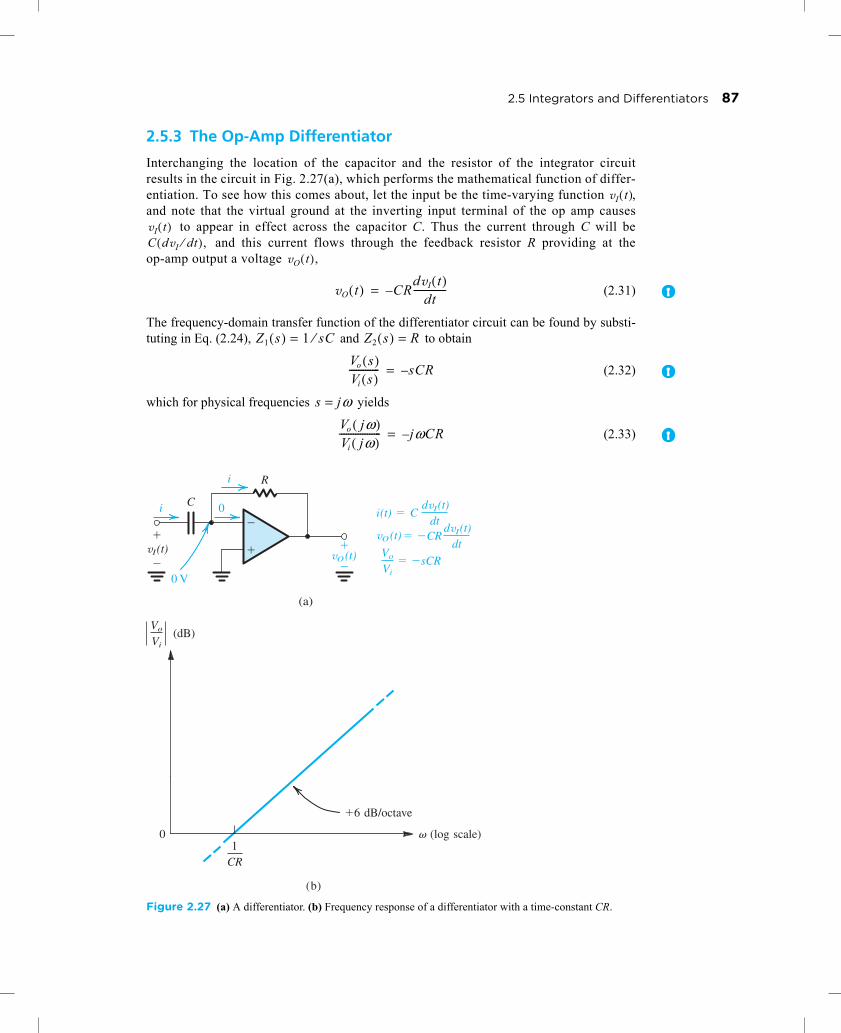
2.5.3 The Op-Amp Differentiator
Interchanging the location of the capacitor and the resistor of the integrator circuitresults in the circuit in Fig. 2.27(a), which performs the mathematical function of differ-entiation. To see how this comes about, let the input be the time-varying function ,and note that the virtual ground at the inverting input terminal of the op amp causes
to appear in effect across the capacitor C. Thus the current through C will be and this current flows through the feedback resistor R providing at the
op-amp output a voltage
(2.31)
The frequency-domain transfer function of the differentiator circuit can be found by substi-tuting in Eq. (2.24), and to obtain
(2.32)
which for physical frequencies yields
(2.33)
Figure 2.27 (a) A differentiator. (b) Frequency response of a differentiator with a time-constant CR.
vI t( )
vI t( )C dvI dt⁄( ),
vO t( ),
vO t( ) CRdvI t( )
dt--------------–=
Z1 s( ) = 1 sC⁄ Z2 s( ) = RVo s( )Vi s( )------------- sCR–=
s = jωVo jω( )Vi jω( )------------------ jωCR–=
�
C
R
Vo
VisCR
vI (t)�
���
�
vO(t)
vO(t)
� �
CR� �
� Ci (t)dvI (t)
dtdvI (t)
dt
(a)
i
i
0
0 V
(b)
(dB)
01
CR
(log scale)
�6 dB/octave
Vo
Vi

88 Chapter 2 Operational Amplifiers
Thus the transfer function has magnitude
(2.34)
and phase
(2.35)
The Bode plot of the magnitude response can be found from Eq. (2.34) by noting that for anoctave increase in ω, the magnitude doubles (increases by 6 dB). Thus the plot is simply astraight line of slope +6 dB/octave (or, equivalently, +20 dB/decade) intersecting the 0-dBline (where at where CR is the differentiator time-constant [seeFig. 2.27(b)].
The frequency response of the differentiator can be thought of as that of an STC highpassfilter with a corner frequency at infinity (refer to Fig. 1.24). Finally, we should note that thevery nature of a differentiator circuit causes it to be a “noise magnifier.” This is due to thespike introduced at the output every time there is a sharp change in such a changecould be interference coupled electromagnetically (“picked up”) from adjacent signalsources. For this reason and because they suffer from stability problems (Chapter 10), differ-entiator circuits are generally avoided in practice. When the circuit of Fig. 2.27(a) is used, itis usually necessary to connect a small-valued resistor in series with the capacitor. Thismodification, unfortunately, turns the circuit into a nonideal differentiator.
2.6 DC Imperfections
Thus far we have considered the op amp to be ideal. The only exception has been a brief dis-cussion of the effect of the op-amp finite gain A on the closed-loop gain of the inverting andnoninverting configurations. Although in many applications the assumption of an ideal op
Vo
Vi----- = ωCR
φ 90°–=
Vo Vi⁄ = 1) ω 1 CR⁄ ,=
vI t( );
2.18 Consider a symmetrical square wave of 20-V peak-to-peak, 0 average, and 2-ms period appliedto a Miller integrator. Find the value of the time constant CR such that the triangular waveform atthe output has a 20-V peak-to-peak amplitude.Ans. 0.5 ms
D2.19 Use an ideal op amp to design an inverting integrator with an input resistance of 10 kΩ and anintegration time constant of 10−3 s. What is the gain magnitude and phase angle of this circuit at10 rad/s and at 1 rad/s? What is the frequency at which the gain magnitude is unity?Ans. R = 10 kΩ, C = 0.1 μF; at ω = 10 rad/s: V/V and φ = +90°; at ω = 1 rad/s:
1,000 V/V and φ = +90°; 1000 rad/sD2.20 Design a differentiator to have a time constant of 10−2 s and an input capacitance of 0.01 μF. What
is the gain magnitude and phase of this circuit at 10 rad/s, and at 103 rad/s? In order to limit thehigh-frequency gain of the differentiator circuit to 100, a resistor is added in series with the ca-pacitor. Find the required resistor value.Ans. C = 0.01 μF; R = 1 MΩ; at ω = 10 rad/s: V/V and φ = −90°; at ω = 1000 rad/s:
V/V and φ = −90°; 10 kΩ
Vo Vi⁄ = 100Vo Vi⁄ =
Vo Vi⁄ = 0.1Vo Vi⁄ = 10
EXERCISES

2.6 DC Imperfections 89
amp is not a bad one, a circuit designer has to be thoroughly familiar with the characteristicsof practical op amps and the effects of such characteristics on the performance of op-amp cir-cuits. Only then will the designer be able to use the op amp intelligently, especially if theapplication at hand is not a straightforward one. The nonideal properties of op amps will, ofcourse, limit the range of operation of the circuits analyzed in the previous examples.
In this and the two sections that follow, we consider some of the important nonidealproperties of the op amp.3 We do this by treating one nonideality at a time, beginning in thissection with the dc problems to which op amps are susceptible.
2.6.1 Offset Voltage
Because op amps are direct-coupled devices with large gains at dc, they are prone to dcproblems. The first such problem is the dc offset voltage. To understand this problem con-sider the following conceptual experiment: If the two input terminals of the op amp are tiedtogether and connected to ground, it will be found that despite the fact that vId = 0, a finite dcvoltage exists at the output. In fact, if the op amp has a high dc gain, the output will be ateither the positive or negative saturation level. The op-amp output can be brought back to itsideal value of 0 V by connecting a dc voltage source of appropriate polarity and magnitudebetween the two input terminals of the op amp. This external source balances out the inputoffset voltage of the op amp. It follows that the input offset voltage (VOS) must be of equalmagnitude and of opposite polarity to the voltage we applied externally.
The input offset voltage arises as a result of the unavoidable mismatches Present in the inputdifferential stage inside the op amp. In later chapters (in particular Chapters 8 and 12) we shallstudy this topic in detail. Here, however, our concern is to investigate the effect of VOS on the oper-ation of closed-loop op-amp circuits. Toward that end, we note that general-purpose op ampsexhibit VOS in the range of 1 mV to 5 mV. Also, the value of VOS depends on temperature. The op-amp data sheets usually specify typical and maximum values for VOS at room temperature as wellas the temperature coefficient of VOS (usually in μV/°C). They do not, however, specify thepolarity of VOS because the component mismatches that give rise to VOS are obviously not known apriori; different units of the same op-amp type may exhibit either a positive or a negative VOS.
To analyze the effect of VOS on the operation of op-amp circuits, we need a circuit modelfor the op amp with input offset voltage. Such a model is shown in Fig. 2.28. It consists of a
3We should note that real op amps have nonideal effects additional to those discussed in this chapter.These include finite (nonzero) common-mode gain or, equivalently, noninfinite CMRR, noninfiniteinput resistance, and nonzero output resistance. The effect of these, however, on the performance ofmost of the closed-loop circuits studied here is not very significant, and their study will be postponedto later chapters (in particular Chapters 8, 9, and 12).
Figure 2.28 Circuit model for an op amp with input offset voltage VOS.

90 Chapter 2 Operational Amplifiers
dc source of value VOS placed in series with the positive input lead of an offset-free op amp.The justification for this model follows from the description above.
Analysis of op-amp circuits to determine the effect of the op-amp VOS on their perfor-mance is straightforward: The input voltage signal source is short-circuited and the opamp is replaced with the model of Fig. 2.28. (Eliminating the input signal, done to sim-plify matters, is based on the principle of superposition.) Following this procedure, wefind that both the inverting and the noninverting amplifier configurations result in thesame circuit, that shown in Fig. 2.29, from which the output dc voltage due to VOS is foundto be
(2.36)
This output dc voltage can have a large magnitude. For instance, a noninverting amplifierwith a closed-loop gain of 1000, when constructed from an op amp with a 5-mV inputoffset voltage, will have a dc output voltage of +5 V or −5 V (depending on the polarityof VOS) rather than the ideal value of 0 V. Now, when an input signal is applied to the
2.21 Use the model of Fig. 2.28 to sketch the transfer characteristic vO versus vId (vO ≡ v3 and vId ≡ v2 −v1) of an op amp having an open-loop dc gain A0 = 104 V/V, output saturation levels of ±10 V, andVOS of +5 mV.Ans. See Fig. E2.21. Observe that true to its name, the input offset voltage causes an offset in thevoltage-transfer characteristic; rather than passing through the origin it is now shifted to the left by VOS.
Figure E2.21 Transfer characteristic of an op amp with VOS = 5 mV.
EXERCISE
VO VOS 1R2
R1-----+=

2.6 DC Imperfections 91
amplifier, the corresponding signal output will be superimposed on the 5-V dc. Obvi-ously then, the allowable signal swing at the output will be reduced. Even worse, if thesignal to be amplified is dc, we would not know whether the output is due to VOS or to thesignal!
Some op amps are provided with two additional terminals to which a specified circuitcan be connected to trim to zero the output dc voltage due to VOS . Figure 2.30 shows suchan arrangement that is typically used with general-purpose op amps. A potentiometer isconnected between the offset-nulling terminals with the wiper of the potentiometer con-nected to the op-amp negative supply. Moving the potentiometer wiper introduces animbalance that counteracts the asymmetry present in the internal op-amp circuitry and thatgives rise to VOS. We shall return to this point in the context of our study of the internal cir-cuitry of op amps in Chapter 12. It should be noted, however, that even though the dc out-put offset can be trimmed to zero, the problem remains of the variation (or drift) of VOSwith temperature.
One way to overcome the dc offset problem is by capacitively coupling the amplifier.This, however, will be possible only in applications where the closed-loop amplifier is notrequired to amplify dc or very-low-frequency signals. Figure 2.31(a) shows a capacitivelycoupled amplifier. Because of its infinite impedance at dc, the coupling capacitor will causethe gain to be zero at dc. As a result the equivalent circuit for determining the dc output
Figure 2.29 Evaluating the output dc offset voltage due to VOS in a closed-loop amplifier.
VO
1 � VO � VOS
VOS
R2
R2
R1R1
Offset-freeop amp
��
�
�
V�
V�
To restof circuit
Offset-nullingterminals
�
�
Figure 2.30 The output dc offset voltage of an op amp can be trimmed to zero by connecting apotentiometer to the two offset-nulling terminals. The wiper of the potentiometer is connected to thenegative supply of the op amp.

92 Chapter 2 Operational Amplifiers
voltage resulting from the op-amp input offset voltage VOS will be that shown in Fig. 2.31(b).Thus VOS sees in effect a unity-gain voltage follower, and the dc output voltage VO will beequal to VOS rather than which is the case without the coupling capacitor.As far as input signals are concerned, the coupling capacitor C forms together with R1 an STChigh-pass circuit with a corner frequency of Thus the gain of the capacitivelycoupled amplifier will fall off at the low-frequency end [from a magnitude of athigh frequencies] and will be 3 dB down at ω0.
Figure 2.31 (a) A capacitively coupled inverting amplifier. (b) The equivalent circuit for determining its dc output offset voltage VO.
(a) (b)
R2
VOS
VO � VOS
��
Offset free
�
�
VOS 1 R2 R1⁄+( ),
ω0 = 1 CR1.⁄1 R2 R1⁄+( )
2.22 Consider an inverting amplifier with a nominal gain of 1000 constructed from an op amp with aninput offset voltage of 3 mV and with output saturation levels of ±10 V. (a) What is (approximately)the peak sine-wave input signal that can be applied without output clipping? (b) If the effect of VOS
is nulled at room temperature (25°C), how large an input can one now apply if: (i) the circuit is tooperate at a constant temperature? (ii) the circuit is to operate at a temperature in the range 0°C to75°C and the temperature coefficient of VOS is 10 μV/°C?Ans. (a) 7 mV; (b) 10 mV, 9.5 mV
2.23 Consider the same amplifier as in Exercise 2.22—that is, an inverting amplifier with a nominal gainof 1000 constructed from an op amp with an input offset voltage of 3 mV and with output saturationlevels of ±10 V—except here let the amplifier be capacitively coupled as in Fig. 2.31(a). (a) Whatis the dc offset voltage at the output, and what (approximately) is the peak sine-wave signal that canbe applied at the input without output clipping? Is there a need for offset trimming? (b) If R1 = 1 kΩand R2 = 1 MΩ, find the value of the coupling capacitor C1 that will ensure that the gain will be greaterthan 57 dB down to 100 Hz.Ans. (a) 3 mV, 10 mV, no need for offset trimming; (b) 1.6 μF
EXERCISES

2.6 DC Imperfections 93
2.6.2 Input Bias and Offset Currents
The second dc problem encountered in op amps is illustrated in Fig. 2.32. In order for the opamp to operate, its two input terminals have to be supplied with dc currents, termed theinput bias currents.4 In Fig. 2.32 these two currents are represented by two current sources,IB1 and IB2, connected to the two input terminals. It should be emphasized that the input biascurrents are independent of the fact that a real op amp has finite (though large) input resis-tance (not shown in Fig. 2.32). The op-amp manufacturer usually specifies the average valueof IB1 and IB2 as well as their expected difference. The average value IB is called the inputbias current,
and the difference is called the input offset current and is given by
Typical values for general-purpose op amps that use bipolar transistors are IB = 100 nA andIOS = 10 nA.
We now wish to find the dc output voltage of the closed-loop amplifier due to theinput bias currents. To do this we ground the signal source and obtain the circuit shown inFig. 2.33 for both the inverting and noninverting configurations. As shown in Fig. 2.33, theoutput dc voltage is given by
(2.37)
This obviously places an upper limit on the value of R2. Fortunately, however, a techniqueexists for reducing the value of the output dc voltage due to the input bias currents. Themethod consists of introducing a resistance R3 in series with the noninverting input lead, as
4This is the case for op amps constructed using bipolar junction transistors (BJTs). Those usingMOSFETs in the first (input) stage do not draw an appreciable input bias current; nevertheless, the inputterminals should have continuous dc paths to ground. More on this in later chapters.
IBIB1 IB2+
2-------------------=
IOS IB1 − IB2=
VO IB1R2 � IBR2=
Figure 2.32 The op-amp input bias currents represented by two current sources IB1 and IB2.

94 Chapter 2 Operational Amplifiers
shown in Fig. 2.34. From a signal point of view, R3 has a negligible effect (ideally no effect).The appropriate value for R3 can be determined by analyzing the circuit in Fig. 2.34, whereanalysis details are shown, and the output voltage is given by
(2.38)
Consider first the case IB1 = IB2 = IB, which results in
Figure 2.33 Analysis of the closed-loop amplifier, taking into account the input bias currents.
Figure 2.34 Reducing the effect of the input bias currents by introducing a resistor R3.
VO − IB2R3 R2 IB1 IB2R3 R1⁄–( )+=
VO IB R2 R3 1 R2 R1⁄+( )–[ ]=

2.6 DC Imperfections 95
Thus we can reduce VO to zero by selecting R3 such that
(2.39)
That is, R3 should be made equal to the parallel equivalent of R1 and R2. Having selected R3 as above, let us evaluate the effect of a finite offset current IOS. Let
and and substitute in Eq. (2.38). The result is
(2.40)
which is usually about an order of magnitude smaller than the value obtained without R3(Eq. 2.37). We conclude that to minimize the effect of the input bias currents, one shouldplace in the positive lead a resistance equal to the equivalant dc resistance seen by theinverting terminal. We emphasize the word dc in the last statement; note that if the ampli-fier is ac-coupled, we should select R3 = R2, as shown in Fig. 2.35.
While we are on the subject of ac-coupled amplifiers, we should note that one mustalways provide a continuous dc path between each of the input terminals of the op ampand ground. This is the case no matter how small IB is. For this reason the ac-couplednoninverting amplifier of Fig. 2.36 will not work without the resistance R3 to ground.Unfortunately, including R3 lowers considerably the input resistance of the closed-loopamplifier.
R3R2
1 R2 R1⁄+------------------------ R1R2
R1 R2+-----------------= =
IB1 = IB IOS 2⁄+ IB2 = IB IOS 2⁄ ,–
VO IOSR2=
Figure 2.35 In an ac-coupled amplifier the dc resistance seen by the inverting terminal is R2; henceR3 is chosen equal to R2.
� R2
Figure 2.36 Illustrating the need for a continuous dc path for each of the op-amp input terminals. Specifi-cally, note that the amplifier will not work without resistor R3.

96 Chapter 2 Operational Amplifiers
2.6.3 Effect of VOS and IOS on the Operation of the Inverting Integrator
Our discussion of the inverting integrator circuit in Section 2.5.2 mentioned the susceptibilityof this circuit to saturation in the presence of small dc voltages or currents. It behooves ustherefore to consider the effect of the op-amp dc offsets on its operation. As will be seen, theseeffects can be quite dramatic.
To see the effect of the input dc offset voltage VOS, consider the integrator circuit in Fig.2.38, where for simplicity we have short-circuited the input signal source. Analysis of thecircuit is straightforward and is shown in Fig. 2.37. Assuming for simplicity that at time t = 0the voltage across the capacitor is zero, the output voltage as a function of time is given by
(2.41)
Thus vO increases linearly with time until the op amp saturates—clearly an unacceptable sit-uation! As should be expected, the dc input offset current IOS produces a similar problem.Figure 2.38 illustrates the situation. Observe that we have added a resistance R in the op-amp positive-input lead in order to keep the input bias current IB from flowing through C.Nevertheless, the offset current IOS will flow through C and cause vO to ramp linearly withtime until the op amp saturates.
As mentioned in Section 2.5.2 the dc problem of the integrator circuit can be allevi-ated by connecting a resistor RF across the integrator capacitor C, as shown in Fig. 2.25.
2.24 Consider an inverting amplifier circuit designed using an op amp and two resistors, R1 = 10 kΩ andR2 = 1 MΩ. If the op amp is specified to have an input bias current of 100 nA and an input offsetcurrent of 10 nA, find the output dc offset voltage resulting and the value of a resistor R3 to be placedin series with the positive input lead in order to minimize the output offset voltage. What is the newvalue of VO?Ans. 0.1 V; 9.9 kΩ (� 10 kΩ); 0.01 V
EXERCISE
vO = VOSVOS
CR-------- t+
�
�
t
Figure 2.37 Determining the effect of the op-amp input offset volage VOS on the Miller integra-tor circuit. Note that since the output rises with time, the op amp eventually saturates.

2.7 Effect of Finite Open-Loop Gain and Bandwidth on Circuit Performance 97
Such a resistor provides a dc path through which the dc currents and IOS canflow, with the result that vO will now have a dc component instead of rising linearly. To keep the dc offset at the output small, one would select alow value for RF. Unfortunately, however, the lower the value of RF, the less ideal theintegrator circuit becomes.
2.7 Effect of Finite Open-Loop Gain and Bandwidth on Circuit Performance
2.7.1 Frequency Dependence of the Open-Loop Gain
The differential open-loop gain A of an op amp is not infinite; rather, it is finite and decreaseswith frequency. Figure 2.39 shows a plot for , with the numbers typical of some commer-cially available general-purpose op amps (such as the popular 741-type op amp, available frommany semiconductor manufacturers; its internal circuit is studied in Chapter 12).
Note that although the gain is quite high at dc and low frequencies, it starts to fall offat a rather low frequency (10 Hz in our example). The uniform –20-dB/decade gain rolloffshown is typical of internally compensated op amps. These are units that have a network(usually a single capacitor) included within the same IC chip whose function is to causethe op-amp gain to have the single-time-constant (STC) low-pass response shown. This
(VOS R⁄ )[VOS 1 RF R⁄+( ) IOSRF]+
vO
R
R IB2
IB1
(IB1 � IB2) � IOS
IB2R�R � IB2
C
vO � �IB2R � IOS
C t
�IB2R
�
�Figure 2.38 Effect of the op-amp input bias and offset currents on the performance of the Miller integrator circuit.
2.25 Consider a Miller integrator with a time constant of 1 ms and an input resistance of 10 kΩ. Let theop amp have VOS = 2 mV and output saturation voltages of ±12 V. (a) Assuming that when thepower supply is turned on the capacitor voltage is zero, how long does it take for the amplifier tosaturate? (b) Select the largest possible value for a feedback resistor RF so that at least ±10 V ofoutput signal swing remains available. What is the corner frequency of the resulting STC net-work?Ans. (a) 6 s; (b) 10 MΩ, 0.16 Hz
EXERCISE
A

98 Chapter 2 Operational Amplifiers
process of modifying the open-loop gain is termed frequency compensation, and itspurpose is to ensure that op-amp circuits will be stable (as opposed to oscillatory). Thesubject of stability of op-amp circuits—or, more generally, of feedback amplifiers—willbe studied in Chapter 10.
By analogy to the response of low-pass STC circuits (see Section 1.6 and, for moredetail, Appendix E), the gain A(s) of an internally compensated op amp may be expressed as
(2.42)
which for physical frequencies, s = jω, becomes
(2.43)
where A0 denotes the dc gain and ωb is the 3-dB frequency (corner frequency or “break” fre-quency). For the example shown in Fig. 2.39, A0 = 105 and ωb = 2π × 10 rad/s. For frequencies ω ωb (about 10 times and higher) Eq. (2.43) may be approximated by
(2.44)
Thus,
(2.45)
from which it can be seen that the gain |A| reaches unity (0 dB) at a frequency denoted by ωt and given by
(2.46)
Figure 2.39 Open-loop gain of a typical general-purpose internally compensated op amp.
A s( )A0
1 s ωb⁄+---------------------=
A jω( )A0
1 jω ωb⁄+-------------------------=
A jω( ) � A0ωb
jω------------
A jω( ) A0ωb
ω------------=
ωt A0ωb=

2.7 Effect of Finite Open-Loop Gain and Bandwidth on Circuit Performance 99
Substituting in Eq. (2.44) gives
(2.47)
The frequency is usually specified on the data sheets of commercially availableop amps and is known as the unity-gain bandwidth.5 Also note that for ω ωb the open-loop gain in Eq. (2.42) becomes
(2.48)
The gain magnitude can be obtained from Eq. (2.47) as
(2.49)
Thus if ft is known (106 Hz in our example), one can easily determine the magnitude of theop-amp gain at a given frequency f. Furthermore, observe that this relationship correlateswith the Bode plot in Fig. 2.39. Specifically, for f fb, doubling f (an octave increase) resultsin halving the gain (a 6-dB reduction). Similarly, increasing f by a factor of 10 (a decadeincrease) results in reducing |A| by a factor of 10 (20 dB).
As a matter of practical importance, we note that the production spread in the value of ftbetween op-amp units of the same type is usually much smaller than that observed for A0 andfb. For this reason ft is preferred as a specification parameter. Finally, it should be mentionedthat an op amp having this uniform –6-dB/octave (or equivalently –20-dB/decade) gainrolloff is said to have a single-pole model. Also, since this single pole dominates the ampli-fier frequency response, it is called a dominant pole. For more on poles (and zeros), the readermay wish to consult Appendix F.
2.7.2 Frequency Response of Closed-Loop Amplifiers
We next consider the effect of limited op-amp gain and bandwidth on the closed-loop transferfunctions of the two basic configurations: the inverting circuit of Fig. 2.5 and the noninvertingcircuit of Fig. 2.12. The closed-loop gain of the inverting amplifier, assuming a finite op-ampopen-loop gain A, was derived in Section 2.2 and given in Eq. (2.5), which we repeat here as
(2.50)
5Since ft is the product of the dc gain A0 and the 3-dB bandwidth fb (where fb = ωb /2π), it is also knownas the gain–bandwidth product (GB). The reader is cautioned, however, that in some amplifiers, theunity-gain frequency and the gain-bandwidth product are not equal.
A jω( ) � ωt
jω------
ft = ωt 2π⁄
A s( ) � ωt
s-----
A jω( ) �ωt
ω----- ft
f--=
Vo
Vi----- R2 R1⁄–
1 1 R2 R1⁄+( ) A⁄+----------------------------------------------=
2.26 An internally compensated op amp is specified to have an open-loop dc gain of 106 dB and a unity-gain bandwidth of 3 MHz. Find fb and the open-loop gain (in dB) at fb, 300 Hz, 3 kHz, 12 kHz, and60 kHz.Ans. 15 Hz; 103 dB; 80 dB; 60 dB; 48 dB; 34 dB
EXERCISE

100 Chapter 2 Operational Amplifiers
Substituting for A from Eq. (2.42) and using Eq. (2.46) gives
(2.51)
For which is usually the case,
(2.52)
which is of the same form as that for a low-pass STC network (see Table 1.2, page 34). Thusthe inverting amplifier has an STC low-pass response with a dc gain of magnitude equal toR2/R1. The closed-loop gain rolls off at a uniform –20-dB/decade slope with a corner fre-quency (3-dB frequency) given by
(2.53)
Similarly, analysis of the noninverting amplifier of Fig. 2.12, assuming a finite open-loopgain A, yields the closed-loop transfer function
(2.54)
Substituting for A from Eq. (2.42) and making the approximation results in
(2.55)
Thus the noninverting amplifier has an STC low-pass response with a dc gain of and a 3-dB frequency given also by Eq. (2.53).
Vo s( )Vi s( )------------- R2 R1⁄–
1 1A0----- 1
R2
R1------+⎝ ⎠
⎛ ⎞ sωt 1 R2 R1⁄+( )⁄---------------------------------------++
-----------------------------------------------------------------------------------=
A0 @ 1 R2 R1⁄ ,+>>Vo s( )Vi s( )------------- R2 R1⁄–
1 sωt 1 R2 R1⁄+( )⁄---------------------------------------+
------------------------------------------------≈
ω3dBωt
1 R2 R1⁄+------------------------=
Vo
Vi----- 1 R2 R1⁄+
1 1 R2 R1⁄+( ) A⁄+----------------------------------------------=
A0 @ 1 R2 R1⁄+>>Vo s( )Vi s( )------------- �
1 R2 R1⁄+
1 sωt 1 R2 R1⁄+( )⁄---------------------------------------+
------------------------------------------------
1 R2 R1⁄+( )
Consider an op amp with ft = 1 MHz. Find the 3-dB frequency of closed-loop amplifiers with nomi-nal gains of +1000, +100, +10, +1, −1, −10, −100, and −1000. Sketch the magnitude frequencyresponse for the amplifiers with closed-loop gains of +10 and –10.
Solution
We use Eq. (2.53) to obtain the results given in the following table.
Closed-Loop Gain R2 ⁄ R1 f3 dB = ft / (1 + R2 ⁄R1)
+1000 999 1 kHz +100 99 10 kHz +10 9 100 kHz +1 0 1 MHz −1 1 0.5 MHz −10 10 90.9 kHz −100 100 9.9 kHz −1000 1000 �1 kHz
Example 2.6
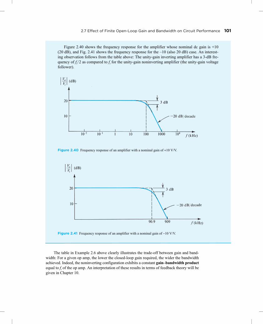
2.7 Effect of Finite Open-Loop Gain and Bandwidth on Circuit Performance 101
The table in Example 2.6 above clearly illustrates the trade-off between gain and band-width: For a given op amp, the lower the closed-loop gain required, the wider the bandwidthachieved. Indeed, the noninverting configuration exhibits a constant gain–bandwidth productequal to ft of the op amp. An interpretation of these results in terms of feedback theory will begiven in Chapter 10.
Figure 2.40 shows the frequency response for the amplifier whose nominal dc gain is +10(20 dB), and Fig. 2.41 shows the frequency response for the –10 (also 20 dB) case. An interest-ing observation follows from the table above: The unity-gain inverting amplifier has a 3-dB fre-quency of ft /2 as compared to ft for the unity-gain noninverting amplifier (the unity-gain voltagefollower).
Figure 2.41 Frequency response of an amplifier with a nominal gain of −10 V/V.
Figure 2.40 Frequency response of an amplifier with a nominal gain of +10 V/V.

102 Chapter 2 Operational Amplifiers
2.8 Large-Signal Operation of Op Amps
In this section, we study the limitations on the performance of op-amp circuits when largeoutput signals are present.
2.8.1 Output Voltage Saturation
Similar to all other amplifiers, op amps operate linearly over a limited range of output volt-ages. Specifically, the op-amp output saturates in the manner shown in Fig. 1.14 with L+ andL– within 1 V or so of the positive and negative power supplies, respectively. Thus, an opamp that is operating from ±15-V supplies will saturate when the output voltage reachesabout +13 V in the positive direction and –13 V in the negative direction. For this particularop amp the rated output voltage is said to be ±13 V. To avoid clipping off the peaks of theoutput waveform, and the resulting waveform distortion, the input signal must be kept corre-spondingly small.
2.8.2 Output Current Limits
Another limitation on the operation of op amps is that their output current is limited to aspecified maximum. For instance, the popular 741 op amp is specified to have a maximumoutput current of ±20 mA. Thus, in designing closed-loop circuits utilizing the 741, thedesigner has to ensure that under no condition will the op amp be required to supply an out-put current, in either direction, exceeding 20 mA. This, of course, has to include both thecurrent in the feedback circuit as well as the current supplied to a load resistor. If the circuitrequires a larger current, the op-amp output voltage will saturate at the level correspondingto the maximum allowed output current.
2.27 An internally compensated op amp has a dc open-loop gain of 106 V/V and an ac open-loop gain of 40dB at 10 kHz. Estimate its 3-dB frequency, its unity-gain frequency, its gain–bandwidth product,and its expected gain at 1 kHz.Ans. 1 Hz; 1 MHz; 1 MHz; 60 dB
2.28 An op amp having a 106-dB gain at dc and a single-pole frequency response with ft = 2 MHz isused to design a noninverting amplifier with nominal dc gain of 100. Find the 3-dB frequency ofthe closed-loop gain.Ans. 20 kHz
EXERCISES

2.8 Large-Signal Operation of Op Amps 103
Consider the noninverting amplifier circuit shown in Fig. 2.42. As shown, the circuit is designed fora nominal gain It is fed with a low-frequency sine-wave signal of peak voltageVp and is connected to a load resistor RL. The op amp is specified to have output saturation voltagesof ±13 V and output current limits of ±20 mA.
(a) For Vp = 1 V and RL = 1 kΩ, specify the signal resulting at the output of the amplifier.(b) For Vp = 1.5 V and RL = 1 kΩ , specify the signal resulting at the output of the amplifier.(c) For RL = 1 kΩ, what is the maximum value of Vp for which an undistorted sine-wave output is
obtained?(d) For Vp = 1 V, what is the lowest value of RL for which an undistorted sine-wave output is
obtained?
Solution
(a) For Vp = 1 V and RL = 1 kΩ, the output will be a sine wave with peak value of 10 V. This islower than output saturation levels of ±13 V, and thus the amplifier is not limited that way. Also,when the output is at its peak (10 V), the current in the load will be kΩ = 10 mA, andthe current in the feedback network will be 10 kΩ = 1 mA, for a total op-amp outputcurrent of 11 mA, well under its limit of 20 mA.
(b) Now if Vp is increased to 1.5 V, ideally the output would be a sine wave of 15-V peak. The opamp, however, will saturate at ±13 V, thus clipping the sine-wave output at these levels. Let’snext check on the op-amp output current: At 13-V output and RL = 1 kΩ, iL = 13 mA and iF =1.3 mA; thus iO = 14.3 mA, again under the 20-mA limit. Thus the output will be a sine wavewith its peaks clipped off at ±13 V, as shown in Fig. 2.42(b).
Figure 2.42 (a) A noninverting amplifier with a nominal gain of 10 V/V designed using an op amp that saturates at±13-V output voltage and has ±20-mA output current limits. (b) When the input sine wave has a peak of 1.5 V, theoutput is clipped off at ±13 V.
1 R2 R1⁄+( ) 10 V/V.=
iF
vO
R2 � 9 k�
1 k�
R1
iO
iL
RL
�
�
��vIt
0
0
Vp
vO15 V
13 V
�15 V
�13 V
t
(a) (b)
10 V 1⁄V 9 1+( )⁄
Example 2.7

104 Chapter 2 Operational Amplifiers
2.8.3 Slew Rate
Another phenomenon that can cause nonlinear distortion when large output signals arepresent is slew-rate limiting. The name refers to the fact that there is a specific maximumrate of change possible at the output of a real op amp. This maximum is known as the slewrate (SR) of the op amp and is defined as
(2.56)
and is usually specified on the op-amp data sheet in units of V/μs. It follows that if the inputsignal applied to an op-amp circuit is such that it demands an output response that is fasterthan the specified value of SR, the op amp will not comply. Rather, its output will change atthe maximum possible rate, which is equal to its SR. As an example, consider an op ampconnected in the unity-gain voltage-follower configuration shown in Fig. 2.43(a), and let theinput signal be the step voltage shown in Fig. 2.43(b). The output of the op amp will not beable to rise instantaneously to the ideal value V; rather, the output will be the linear ramp ofslope equal to SR, shown in Fig. 2.43(c). The amplifier is then said to be slewing, and itsoutput is slew-rate limited.
In order to understand the origin of the slew-rate phenomenon, we need to know aboutthe internal circuit of the op amp, and we will study it in Chapter 12. For the time being,however, it is sufficient to know about the phenomenon and to note that it is distinct fromthe finite op-amp bandwidth that limits the frequency response of the closed-loop amplifi-ers, studied in the previous section. The limited bandwidth is a linear phenomenon anddoes not result in a change in the shape of an input sinusoid; that is, it does not lead to non-linear distortion. The slew-rate limitation, on the other hand, can cause nonlinear distortionto an input sinusoidal signal when its frequency and amplitude are such that the corre-sponding ideal output would require vO to change at a rate greater than SR. This is the ori-gin of another related op-amp specification, its full-power bandwidth, to be explained later.
Before leaving the example in Fig. 2.43, however, we should point out that if the stepinput voltage V is sufficiently small, the output can be the exponentially rising ramp shown inFig. 2.43(d). Such an output would be expected from the follower if the only limitation on itsdynamic performance were the finite op-amp bandwidth. Specifically, the transfer function ofthe follower can be found by substituting R1 = ∞ and R2 = 0 in Eq. (2.55) to obtain
(2.57)
SR dvO
dt---------
max
=
Vo
Vi----- 1
1 s ωt⁄+---------------------=
Example 2.7 continued
(c) For RL = 1 kΩ, the maximum value of Vp for undistorted sine-wave output is 1.3 V. The outputwill be a 13-V peak sine wave, and the op-amp output current at the peaks will be 14.3 mA.
(d) For Vp = 1 V and RL reduced, the lowest value possible for RL while the output is remaining anundistorted sine wave of 10-V peak can be found from
which results in
iOmax 20 mA 10 VRLmin------------== 10 V
9 kΩ 1 kΩ+--------------------------------+
RLmin 526 Ω=

2.8 Large-Signal Operation of Op Amps 105
which is a low-pass STC response with a time constant Its step response would there-fore be (see Appendix E)
(2.58)
The initial slope of this exponentially rising function is (ωtV). Thus, as long as V is suffi-ciently small so that ωtV ≤ SR, the output will be as in Fig. 2.43(d).
t0
v1
V
(b)
t0
vO
Slope � SR V
(c)
t0
vO
Slope � tV � SR
V
(d)
Figure 2.43 (a) Unity-gain follower. (b) Input step waveform. (c) Linearly rising output waveformobtained when the amplifier is slew-rate limited. (d) Exponentially rising output waveform obtained whenV is sufficiently small so that the initial slope (ωtV) is smaller than or equal to SR.
1 ωt⁄ .
vO t( ) V 1 e ωt t––( )=
2.29 An op amp that has a slew rate of 1 V/μs and a unity-gain bandwidth ft of 1 MHz is connected in theunity-gain follower configuration. Find the largest possible input voltage step for which the outputwaveform will still be given by the exponential ramp of Eq. (2.58). For this input voltage, what isthe 10% to 90% rise time of the output waveform? If an input step 10 times as large is applied, findthe 10% to 90% rise time of the output waveform.Ans. 0.16 V; 0.35 μs; 1.28 μs
EXERCISE

106 Chapter 2 Operational Amplifiers
2.8.4 Full-Power Bandwidth
Op-amp slew-rate limiting can cause nonlinear distortion in sinusoidal waveforms. Consideronce more the unity-gain follower with a sine-wave input given by
The rate of change of this waveform is given by
with a maximum value of This maximum occurs at the zero crossings of the inputsinusoid. Now if exceeds the slew rate of the op amp, the output waveform will bedistorted in the manner shown in Fig. 2.44. Observe that the output cannot keep up with thelarge rate of change of the sinusoid at its zero crossings, and the op amp slews.
The op-amp data sheets usually specify a frequency fM called the full-power bandwidth.It is the frequency at which an output sinusoid with amplitude equal to the rated output volt-age of the op amp begins to show distortion due to slew-rate limiting. If we denote the ratedoutput voltage then fM is related to SR as follows:
Thus,
(2.59)
It should be obvious that output sinusoids of amplitudes smaller than will show slew-rate distortion at frequencies higher than ωM . In fact, at a frequency ω higher than ωM , themaximum amplitude of the undistorted output sinusoid is given by
(2.60)
Figure 2.44 Effect of slew-rate limiting on output sinusoidal waveforms.
vI Vi sinωt=
dvI
dt------- ωVi cosωt=
ωVi.ωVi
Vomax,
ωMVomax SR=
fMSR
2π Vomax-------------------=
Vomax
Vo VomaxωM
ω-------⎝ ⎠⎛ ⎞=

2.8 Large-Signal Operation of Op Amps 107
2.30 An op amp has a rated output voltage of ±10 V and a slew rate of 1 V/μs. What is its full-powerbandwidth? If an input sinusoid with frequency f = 5fM is applied to a unity-gain follower con-structed using this op amp, what is the maximum possible amplitude that can be accommodatedat the output without incurring SR distortion?Ans. 15.9 kHz; 2 V (peak)
EXERCISE
Summary
The IC op amp is a versatile circuit building block. It iseasy to apply, and the performance of op-amp circuitsclosely matches theoretical predictions.
The op-amp terminals are the inverting input terminal(1), the noninverting input terminal (2), the output ter-minal (3), the positive-supply terminal (4) to be con-nected to the positive power supply (VCC), and thenegative-supply terminal (5) to be connected to thenegative supply (−VEE). The common terminal of thetwo supplies is the circuit ground.
The ideal op amp responds only to the difference inputsignal, that is, providing at the output, be-tween terminal 3 and ground, a signal whereA, the open-loop gain, is very large (104 to 106) and ide-ally infinite; and has an infinite input resistance and azero output resistance. (See Table 3.1.)
Negative feedback is applied to an op amp by connectinga passive component between its output terminal and itsinverting (negative) input terminal. Negative feedbackcauses the voltage between the two input terminals tobecome very small and ideally zero. Correspondingly, avirtual short circuit is said to exist between the two inputterminals. If the positive input terminal is connected toground, a virtual ground appears on the negative inputterminal.
The two most important assumptions in the analysis ofop-amp circuits, presuming negative feedback existsand the op amps are ideal, are as follows: the two inputterminals of the op amp are at the same voltage, andzero current flows into the op-amp input terminals.
With negative feedback applied and the loop closed,the closed-loop gain is almost entirely determined byexternal components: For the inverting configuration,
and for the noninverting configuration,
The noninverting closed-loop configuration features a veryhigh input resistance. A special case is the unity-gain fol-lower, frequently employed as a buffer amplifier to con-nect a high-resistance source to a low-resistance load.
The difference amplifier of Fig. 2.16 is designed with, resulting in
.
The instrumentation amplifier of Fig. 2.20(b) is a verypopular circuit. It provides
. It is usually designed with , and and selected to provide the required gain. If an adjust-able gain is needed, part of can be made variable.
The inverting Miller integrator of Fig. 2.24 is a popular cir-cuit, frequently employed in analog signal-processing func-tions such as filters (Chapter 16) and oscillators (Chapter 17).
The input offset voltage, VOS , is the magnitude of dc volt-age that when applied between the op amp input termi-nals, with appropriate polarity, reduces the dc offsetvoltage at the output to zero.
The effect of VOS on performance can be evaluated byincluding in the analysis a dc source VOS in series withthe op-amp positive input lead. For both the invertingand the noninverting configurations, VOS results in a dcoffset voltage at the output of
Capacitively coupling an op amp reduces the dc offsetvoltage at the output considerably.
The average of the two dc currents, IB1 and IB2, that flow inthe input terminals of the op amp, is called the input biascurrent, IB. In a closed-loop amplifier, IB gives rise to a dcoffset voltage at the output of magnitude IBR2. This voltagecan be reduced to IOS R2 by connecting a resistance in se-ries with the positive input terminal equal to the total dc re-sistance seen by the negative input terminal. IOS is the inputoffset current; that is,
v2 v1–( );A v2 v1–( ),“
Vo Vi⁄ R2 R1;⁄–=Vo Vi⁄ 1 R2 R1.⁄+=
R4 R3⁄ R2 R1⁄= vO R2 R1⁄( )=vI2 vI1–( )
vO 1 R2 R1⁄+( ) R4 R3⁄( )=vI2 vI1–( ) R3 R4= R1
R2R1
VOS 1 R2 R1⁄+( ).
IOS IB1 IB2– .=

108 Chapter 2 Operational Amplifiers
Connecting a large resistance in parallel with the capaci-tor of an op-amp inverting integrator prevents op-ampsaturation (due to the effect of VOS and IB).
For most internally compensated op amps, the open-loopgain falls off with frequency at a rate of −20 dB/decade,reaching unity at a frequency ft (the unity-gain band-width). Frequency ft is also known as the gain–bandwidthproduct of the op amp: ft = A0 fb, where A0 is the dc gain,and fb is the 3-dB frequency of the open-loop gain. At anyfrequency f ( f fb), the op-amp gain
For both the inverting and the noninverting closed-loopconfigurations, the 3-dB frequency is equal to
The maximum rate at which the op-amp output voltagecan change is called the slew rate. The slew rate, SR, isusually specified in V/μs. Op-amp slewing can result innonlinear distortion of output signal waveforms.
The full-power bandwidth, fM, is the maximum frequencyat which an output sinusoid with an amplitude equal tothe op-amp rated output voltage (Vomax) can be producedwithout distortion:
A � ft f.⁄
ft 1 R2 R1⁄+( )⁄ .
fM SR 2πVomax.⁄=
PROBLEMS
Computer Simulation Problems
Problems identified by this icon are intended to dem-onstrate the value of using SPICE simulation to verify handanalysis and design, and to investigate important issues suchas allowable signal swing and amplifier nonlinear distortion.Instructions to assist in setting up PSpice and Multism simu-lations for all the indicated problems can be found in thecorresponding files on the disc. Note that if a particularparameter value is not specified in the problem statement,you are to make a reasonable assumption. * difficult prob-lem; ** more difficult; *** very challenging and/or time-consuming; D: design problem.
Section 2.1: The Ideal Op Amp
2.1 What is the minimum number of pins required for a so-called dual-op-amp IC package, one containing two opamps? What is the number of pins required for a so-calledquad-op-amp package, one containing four op-amps?
2.2 The circuit of Fig. P2.2 uses an op amp that is idealexcept for having a finite gain A. Measurements indicatevO = 4.0 V when vI = 2.0 V. What is the op-amp gain A?
2.3 Measurement of a circuit incorporating what is thoughtto be an ideal op amp shows the voltage at the op-amp outputto be −2.000 V and that at the negative input to be −1.000 V.For the amplifier to be ideal, what would you expect the volt-age at the positive input to be? If the measured voltage at thepositive input is −1.010 V, what is likely to be the actual gainof the amplifier?
2.4 A set of experiments is run on an op amp that is idealexcept for having a finite gain A. The results are tabulatedbelow. Are the results consistent? If not, are they reason-able, in view of the possibility of experimental error? Whatdo they show the gain to be? Using this value, predict valuesof the measurements that were accidentally omitted (the blankentries).
Experiment # v1 v2 vO
1 0.00 0.00 0.002 1.00 1.00 0.003 1.00 1.004 1.00 1.10 10.15 2.01 2.00 −0.996 1.99 2.00 1.007 5.10 −5.10
Figure P2.2

Problems 109
CH
AP
TE
R 2
PR
OB
LE
MS
2.5 Refer to Exercise 2.3. This problem explores an alter-native internal structure for the op amp. In particular, wewish to model the internal structure of a particular op ampusing two transconductance amplifiers and one transresistanceamplifier. Suggest an appropriate topology. For equaltransconductances Gm and a transresistance Rm, find anexpression for the open-loop gain A. For Gm = 10 mA/V andRm = 2 � 106 Ω, what value of A results?
2.6 The two wires leading from the output terminals of atransducer pick up an interference signal that is a 60-Hz, 1-V sinusoid. The output signal of the transducer is sinusoi-dal of 10-mV amplitude and 1000-Hz frequency. Giveexpressions for vcm, vd, and the total signal between eachwire and the system ground.
2.7 Nonideal (i.e., real) operational amplifiers respondto both the differential and common-mode components oftheir input signals (refer to Fig. 2.4 for signal representa-tion). Thus the output voltage of the op amp can beexpressed as
where Ad is the differential gain (referred to simply as Ain the text) and Acm is the common-mode gain (assumed tobe zero in the text). The op amp’s effectiveness in reject-ing common-mode signals is measured by its CMRR,defined as
Consider an op amp whose internal structure is of the typeshown in Fig. E2.3 except for a mismatch ΔGm between thetransconductances of the two channels; that is,
Find expressions for Ad , Acm, and CMRR. If Ad is 80 dB andthe two transconductances are matched to within 0.1% ofeach other, calculate Acm and CMRR.
Section 2.2: The Inverting Configuration
2.8 Assuming ideal op amps, find the voltage gainand input resistance Rin of each of the circuits in
Fig. P2.8.
2.9 A particular inverting circuit uses an ideal op ampand two 10-kΩ resistors. What closed-loop gain wouldyou expect? If a dc voltage of +1.00 V is applied at theinput, what output result? If the 10-kΩ resistors are said tobe “1% resistors,” having values somewhere in the range(1 ± 0.01) times the nominal value, what range of outputswould you expect to actually measure for an input of pre-cisely 1.00 V?
2.10 You are provided with an ideal op amp and three 10-kΩ resistors. Using series and parallel resistor combinations,how many different inverting-amplifier circuit topologies arepossible? What is the largest (noninfinite) available voltage
vO AdvId AcmvIcm+=
CMRR = 20 log Ad
Acm--------
Gm1 Gm12--- GmΔ–=
Gm2 Gm12--- GmΔ+=
vo vi⁄
(a) (b)
(c) (d)
�
�
�
�
�
�
�
�
Figure P2.8

CH
AP
TE
R 2
PR
OB
LE
MS
110 Chapter 2 Operational Amplifiers
gain? What is the smallest (nonzero) available gain? Whatare the input resistances in these two cases?
2.11 For ideal op amps operating with the followingfeedback networks in the inverting configuration, what closed-loop gain results?
(a)(b)(c)(d)(e)
D 2.12 Given an ideal op amp, what are the values of theresistors R1 and R2 to be used to design amplifiers with theclosed-loop gains listed below? In your designs, use at leastone 10-kΩ resistor and another equal or larger resistor.
(a) −1 V/V(b) −2 V/V(c) −0.5 V/V(d) −100 V/V
D 2.13 Design an inverting op-amp circuit for which thegain is −4 V/V and the total resistance used is 100 kΩ.
D 2.14 Using the circuit of Fig. 2.5 and assuming an idealop amp, design an inverting amplifier with a gain of 26 dBhaving the largest possible input resistance under the con-straint of having to use resistors no larger than 1 MΩ. Whatis the input resistance of your design?
2.15 An ideal op amp is connected as shown in Fig. 2.5with R1 = 10 kΩ and R2 = 100 kΩ. A symmetrical square-wave signal with levels of 0 V and 1 V is applied at theinput. Sketch and clearly label the waveform of the resultingoutput voltage. What is its average value? What is its high-est value? What is its lowest value?
2.16 For the circuit in Fig. P2.16, assuming an ideal opamp, find the currents through all branches and the voltagesat all nodes. Since the current supplied by the op amp isgreater than the current drawn from the input signal source,where does the additional current come from?
2.17 An inverting op-amp circuit is fabricated with theresistors R1 and R2 having x% tolerance (i.e., the value ofeach resistance can deviate from the nominal value by asmuch as ± x%). What is the tolerance on the realized closed-loop gain? Assume the op amp to be ideal. If the nominalclosed-loop gain is −100 V/V and x = 1, what is the range ofgain values expected from such a circuit?
2.18 An ideal op amp with 5-kΩ and 15-kΩ resistors isused to create a +5-V supply from a −15-V reference.Sketch the circuit. What are the voltages at the ends of the 5-kΩ resistor? If these resistors are so-called 1% resistors,whose actual values are the range bounded by the nominalvalue ±1%, what are the limits of the output voltage pro-duced? If the −15-V supply can also vary by ±1%, what isthe range of the output voltages that might be found?
2.19 An inverting op-amp circuit for which the required gainis −50 V/V uses an op amp whose open-loop gain is only300 V/V. If the larger resistor used is 100 kΩ, to what must thesmaller be adjusted? With what resistor must a 2-kΩ resistorconnected to the input be shunted to achieve this goal? (Notethat a resistor Ra is said to be shunted by resistor Rb when Rb isplaced in parallel with Ra.)
D 2.20 (a) Design an inverting amplifier with a closed-loop gain of −100 V/V and an input resistance of 1 kΩ.(b) If the op amp is known to have an open-loop gain of2000 V/V, what do you expect the closed-loop gain ofyour circuit to be (assuming the resistors have precisevalues)?(c) Give the value of a resistor you can place in parallel(shunt) with R1 to restore the closed-loop gain to its nominalvalue. Use the closest standard 1% resistor value (seeAppendix H).
2.21 An op amp with an open-loop gain of 2000 V/V isused in the inverting configuration. If in this application theoutput voltage ranges from −10 V to +10 V, what is themaximum voltage by which the “virtual ground node”departs from its ideal value?
2.22 The circuit in Fig. P2.22 is frequently used to providean output voltage vo proportional to an input signal current ii.
R1 = 10 kΩ, R2 = 10 kΩR1 = 10 kΩ, R2 = 100 kΩR1 = 10 kΩ, R2 = 1 kΩR1 = 100 kΩ, R2 = 10 MΩR1 = 100 kΩ, R2 = 1 MΩ
10 kV
2 kV
1 kV2
11220.5 V
Figure P2.16
vo1
2vi
Figure P2.22

Problems 111
CH
AP
TE
R 2
PR
OB
LE
MS
Derive expressions for the transresistance andthe input resistance for the following cases:
(a) A is infinite.(b) A is finite.
2.23 Show that for the inverting amplifier if the op-ampgain is A, the input resistance is given by
*2.24 For an inverting amplifier with nominal closed-loopgain , find the minimum value that the op-amp open-loop gain A must have (in terms of ) so that the gainerror is limited to 0.1%, 1%, and 10%. In each case find thevalue of a resistor RIa such that when it is placed in shuntwith Ri , the gain is restored to its nominal value.
*2.25 Figure P2.25 shows an op amp that is ideal except forhaving a finite open-loop gain and is used to realize an invert-ing amplifier whose gain has a nominal magnitude
To compensate for the gain reduction due to thefinite A, a resistor Rc is shunted across R1. Show that perfectcompensation is achieved when Rc is selected according to
Figure P2.25
*D 2.26 (a) Use Eq. (2.5) to obtain the amplifier open-loopgain A required to realize a specified closed-loop gain
within a specified gain error ε,
(b) Design an inverting amplifer for a nominal closed-loopgain of −100, an input resistance of 2 kΩ, and a gain error of
10%. Specify R1, R2 , and the minimum A required.
*2.27 (a) Use Eq. (2.5) to show that a reduction in the op-amp gain A gives rise to a reduction in the magnitude ofthe closed-loop gain G with and related by
(b) If in a closed-loop amplifier with a nominal gain (i.e,) of 100, A decreases by 50%, what is the minimum
nominal A required to limit the percentage change in to0.5%?
2.28 Consider the circuit in Fig. 2.8 with R1 = R2 = R4 =1 MΩ, and assume the op amp to be ideal. Find values for R3
to obtain the following gains:
(a) −200 V/V(b) −20 V/V(c) −2 V/V
D 2.29 An inverting op-amp circuit using an ideal op ampmust be designed to have a gain of −1000 V/V using resis-tors no larger than 100 kΩ.
(a) For the simple two-resistor circuit, what input resis-tance would result?(b) If the circuit in Fig. 2.8 is used with three resistors ofmaximum value, what input resistance results? What isthe value of the smallest resistor needed?
2.30 The inverting circuit with the T network in the feed-back is redrawn in Fig. P2.30 in a way that emphasizes theobservation that R2 and R3 in effect are in parallel (becausethe ideal op amp forces a virtual ground at the invertinginput terminal). Use this observation to derive an expressionfor the gain by first finding and For the latter use the voltage-divider rule applied to R4 and(R2 || R3).
*2.31 The circuit in Fig. P2.31 can be considered to be anextension of the circuit in Fig. 2.8.
(a) Find the resistances looking into node 1, R1; node 2,R2; node 3, R3; and node 4, R4.(b) Find the currents I1, I2, I3, and I4, in terms of the inputcurrent I.(c) Find the voltages at nodes 1, 2, 3, and 4, that is, V1, V2,V3, and V4 in terms of (IR).
Rm vo ii⁄≡Ri vi ii⁄≡
Rin R1R2
A 1+-------------+=
R2 R1⁄R2 R1⁄
G R2 R1⁄= .
Rc
R1----- A G–
1 G+--------------=
Vi
R2
R1
Rc
Vo
�
�
Gnominal R– 2 R1⁄=( )
ε G Gnominal–Gnominal
----------------------------≡
≤
AΔGΔ
GΔ AΔ
G G⁄ΔA A⁄Δ
---------------------- 1 R2 R1⁄+A
-------------------------=
R2 R1⁄G
vO vI⁄( ) vX vI⁄( ) vO vX⁄( ).
0 VvI
vX
vO
iI
R2 R4
R3
R1
�
�
Figure P2.30

CH
AP
TE
R 2
PR
OB
LE
MS
112 Chapter 2 Operational Amplifiers
2.32 The circuit in Fig. P2.32 utilizes an ideal op amp.
(a) Find I1, I2, I3, IL, and Vx.(b) If VO is not to be lower than −13 V, find the maximumallowed value for RL.(c) If RL is varied in the range 100 Ω to 1 kΩ, what is thecorresponding change in IL and in VO?
2.33 Use the circuit in Fig. P2.32 as an inspiration todesign a circuit that supplies a constant current I of 3.1 mAto a variable resistance RL. Assume the availability of a1.5 V battery and design so that the current drawn from thebattery is 0.1 mA. For the smallest resistance in the circuit,use 500 Ω. If the op amp saturates at ±12 V, what is themaximum value that RL can have while the current-sourcesupplying it operates properly?
D 2.34 Assuming the op amp to be ideal, it is required todesign the circuit shown in Fig. P2.34 to implement a cur-rent amplifier with gain
(a) Find the required value for R.(b) What are the input and the output resistance of thiscurrent amplifier?
(c) If RL = 1 kΩ and the op amp operates in an ideal man-ner as long as vO is in the range ±12 V, what range of iI ispossible?(d) If the amplifier is fed with a current source having acurrent of 0.2 mA and a source resistance of 10 kΩ, find iL.
D 2.35 Design the circuit shown in Fig. P2.35 to have aninput resistance of 100 kΩ and a gain that can be varied
1
0 V
R
2
1
I1
R1
2R/2
I2
R2
3R/2
R R R
I3
R3
4R/2
I4
R4I
Ideal
Figure P2.31
1 V
VX
VO
I1
10 kV
10 kV
100 V
RL
2
1
I2
I3
IL
Figure P2.32
iL iI⁄ 10 A/A.=
vO
iI
10 kV
R
RL
2
1
iL
Figure P2.34
vO
vI
R2R4
R12
1
R3
Figure P2.35

Problems 113
CH
AP
TE
R 2
PR
OB
LE
MS
from −1 V/V to −10 V/V using the 10-kΩ potentiometer R4.What voltage gain results when the potentiometer is setexactly at its middle value?
2.36 A weighted summer circuit using an ideal op amp hasthree inputs using 100-kΩ resistors and a feedback resistor of50 kΩ. A signal v1 is connected to two of the inputs while asignalv2 is connected to the third. Express vO in terms of v1
and v2. If v1 = 2 V and v2 = –2 V, what is vO?
D 2.37 Design an op amp circuit to provide an output Choose relatively low values of
resistors but ones for which the input current (from eachinput signal source) does not exceed 0.1 mA for 1-V inputsignals.
D 2.38 Use the scheme illustrated in Fig. 2.10 to design anop-amp circuit with inputs v1, v2, and v3, whose output isvO = −(2v1 + 4v2 + 8v3) using small resistors but no smallerthan 10 kΩ.
D 2.39 An ideal op amp is connected in the weightedsummer configuration of Fig. 2.10. The feedback resistorRf = 10 kΩ, and six 10-kΩ resistors are connected to theinverting input terminal of the op amp. Show, by sketchingthe various circuit configurations, how this basic circuitcan be used to implement the following functions:
(a)(b)(c)(d)
In each case find the input resistance seen by each of thesignal sources supplying v1, v2, v3, and v4. Suggest at leasttwo additional summing functions that you can realize withthis circuit. How would you realize a summing coefficientthat is 0.5?
D 2.40 Give a circuit, complete with component values, fora weighted summer that shifts the dc level of a sine-wave sig-nal of 3 sin(ω t) V from zero to −3 V. Assume that in additionto the sine-wave signal you have a dc reference voltage of1.5 V available. Sketch the output signal waveform.
D 2.41 Use two ideal op amps and resistors to implementthe summing function
D *2.42 In an instrumentation system, there is a need totake the difference between two signals, one of v1 =2 sin(2π × 60t) + 0.01 sin(2π × 1000t) volts and anotherof v2 = 2 sin(2π × 60t) − 0.01 sin(2π × 1000t) volts. Drawa circuit that finds the required difference using two opamps and mainly 100-kΩ resistors. Since it is desirable toamplify the 1000-Hz component in the process, arrange toprovide an overall gain of 100 as well. The op amps
available are ideal except that their output voltage swing islimited to ±10 V.
*2.43 Figure P2.43 shows a circuit for a digital-to-analogconverter (DAC). The circuit accepts a 4-bit input binaryword a3a2a1a0, where a0, a1, a2, and a3 take the values of 0or 1, and it provides an analog output voltage vO propor-tional to the value of the digital input. Each of the bits ofthe input word controls the correspondingly numberedswitch. For instance, if a2 is 0 then switch S2 connects the20-kΩ resistor to ground, while if a2 is 1 then S2 connectsthe 20-kΩ resistor to the +5-V power supply. Show that vO
is given by
where Rf is in kilohms. Find the value of Rf so that vO rangesfrom 0 to −12 volts.
Section 2.3: The Noninverting Configuration
D 2.44 Given an ideal op amp to implement designs forthe following closed-loop gains, what values of resistors (R1,R2) should be used? Where possible, use at least one 10-kΩresistor as the smallest resistor in your design.
vO 2v1 v2 2⁄( )+[ ].–=
vO v1 2v2 3v3+ +( )–=vO v1 v2 2v3 2v4+ + +( )–=vO v1 5v2+( )–=vO 6– v1=
vO v1 2v2 3v3– 4v4–+=
vORf
16------ 20a0 21a1 22a2 23a3+ + +[ ]–=
Figure P2.43

CH
AP
TE
R 2
PR
OB
LE
MS
114 Chapter 2 Operational Amplifiers
(a) +1 V/V(b) +2 V/V(c) +11 V/V(d) +100 V/V
D 2.45 Design a circuit based on the topology of the non-inverting amplifier to obtain a gain of +1.5 V/V, using only10-kΩ resistors. Note that there are two possibilities. Whichof these can be easily converted to have a gain of either +1.0V/V or +2.0 V/V simply by short-circuiting a single resistorin each case?
D 2.46 Figure P2.46 shows a circuit for an analog voltme-ter of very high input resistance that uses an inexpensivemoving-coil meter. The voltmeter measures the voltage Vapplied between the op amp’s positive-input terminal andground. Assuming that the moving coil produces full-scaledeflection when the current passing through it is 100 μA,find the value of R such that full-scale reading is obtainedwhen V is +10 V. Does the meter resistance shown affect thevoltmeter calibration?
Figure P2.46
D *2.47 (a) Use superposition to show that the output ofthe circuit in Fig. P2.47 is given by
where RN = RN1||RN2|| . . . ||RNn and
RP = RP1||RP2|| . . . ||RPn||RP0
(b) Design a circuit to obtain
The smallest resistor used should be 10 kΩ.
D 2.48 Design a circuit, using one ideal op amp, whose out-put is vO = vI1 + 3vI2 – 2(vI3 + 3vI4). (Hint: Use a structure sim-ilar to that shown in general form in Fig. P2.47.)
2.49 Derive an expression for the voltage gain, ofthe circuit in Fig. P2.49.
2.50 For the circuit in Fig. P2.50, use superposition to findvO in terms of the input voltages v1 and v2. Assume an idealop amp. For
find vO.
D 2.51 The circuit shown in Fig. P2.51 utilizes a 10-kΩpotentiometer to realize an adjustable-gain amplifier. Derivean expression for the gain as a function of the potentiometer
V
vORf
RN1--------vN1
Rf
RN2--------vN2 . . . Rf
RNn--------vNn+ + +–=
1Rf
RN------++
RP
RP1--------vP1
RP
RP2--------vP2 . . . RP
RPn--------vPn+ + +
vO 3vN1– vP1 2vP2+ +=
RP0
Figure P2.47
vO vI⁄ ,
R2
R4
R1
R3
2
1 1
2
vO1
2
vI
Figure P2.49
v1 = 10 2π × 60t( ) 0.1sin 2π × 1000t( ) volts,–sinv2 = 10 2π 60t×( ) 0.1sin 2π × 1000t( ) volts,+sin

Problems 115
CH
AP
TE
R 2
PR
OB
LE
MS
setting x. Assume the op amp to be ideal. What is the rangeof gains obtained? Show how to add a fixed resistor so thatthe gain range can be 1 to 11 V/V. What should the resistorvalue be?
D 2.52 Given the availability of resistors of value 1 kΩand 10 kΩ only, design a circuit based on the noninvertingconfiguration to realize a gain of +10 V/V.
2.53 It is required to connect a 10-V source with a sourceresistance of 100 kΩ to a 1-kΩ load. Find the voltage thatwill appear across the load if:
(a) The source is connected directly to the load. (b) A unity-gain op-amp buffer is inserted between thesource and the load.
In each case find the load current and the current suppliedby the source. Where does the load current come from incase (b)?
2.54 Derive an expression for the gain of the voltage fol-lower of Fig. 2.14, assuming the op amp to be ideal exceptfor having a finite gain A. Calculate the value of theclosed-loop gain for A = 1000, 100, and 10. In each casefind the percentage error in gain magnitude from the nomi-nal value of unity.
2.55 Complete the following table for feedback amplifierscreated using one ideal op amp. Note that Rin signifies inputresistance and R1 and R2 are feedback-network resistors aslabelled in the inverting and noninverting configurations.
D 2.56 A noninverting op-amp circuit with nominal gainof 10 V/V uses an op amp with open-loop gain of 50 V/Vand a lowest-value resistor of 10 kΩ. What closed-loop gainactually results? With what value resistor can which resistorbe shunted to achieve the nominal gain? If in the manufac-turing process, an op amp of gain 100 V/V were used, whatclosed-loop gain would result in each case (the uncompen-sated one, and the compensated one)?
2.57 Use Eq. (2.11) to show that if the reduction in theclosed-loop gain G from the nominal value is to be kept less than x% of G0, then the open-loop gainof the op amp must exceed G0 by at least a factor F =
Find the required F for x = 0.01,0.1, 1, and 10. Utilize these results to find for each value of xthe minimum required open-loop gain to obtain closed-loopgains of 1, 10, 102, 103, and 104 V/V.
2.58 For each of the following combinations of op-ampopen-loop gain A and nominal closed-loop gain G0, calculatethe actual closed-loop gain G that is achieved. Also, calcu-late the percentage by which falls short of the nominalgain magnitude
20R
20R
Figure P2.50
Figure P2.51
Case Gain Rin R1 R2
a −10 V/V 10 kΩb −1 V/V 100 kΩc −2 V/V 100 kΩd +1 V/V ∞e +2 V/V 10 kΩf +11 V/V 100 kΩg −0.5 V/V 10 kΩ
G0 1 R2 R1⁄+=
(100 x) 1–⁄ � 100 x⁄ .
G
Case G0 (V/V) A (V/V)
a −1 10b +1 10c −1 100d +10 10e −10 100f −10 1000g +1 2
G0 .

CH
AP
TE
R 2
PR
OB
LE
MS
116 Chapter 2 Operational Amplifiers
2.59 Figure P2.59 shows a circuit that provides an outputvoltage vO whose value can be varied by turning the wiperof the 100-kΩ potentiometer. Find the range over whichvO can be varied. If the potentiometer is a “20-turn” device,find the change in vO corresponding to each turn of the pot.
Figure P2.59
Section 2.4: Difference Amplifiers
2.60 Find the voltage gain for the differenceamplifier of Fig. 2.16 for the case R1 = R3 = 10 kΩ and R2 =R4 = 100 kΩ. What is the differential input resistance Rid? Ifthe two key resistance ratios and are dif-ferent from each other by 1%, what do you expect thecommon-mode gain Acm to be? Also, find the CMRR in thiscase. Neglect the effect of the ratio mismatch on the valueof Ad .
D 2.61 Using the difference amplifier configuration ofFig. 2.16 and assuming an ideal op amp, design the circuitto provide the following differential gains. In each case, thedifferential input resistance should be 20 kΩ.
(a) 1 V/V(b) 2 V/V(c) 100 V/V(d) 0.5 V/V
2.62 For the circuit shown in Fig. P2.62, express vO as afunction of v1 and v2. What is the input resistance seen by v1
alone? By v2 alone? By a source connected between the twoinput terminals? By a source connected to both input termi-nals simultaneously?
2.63 Consider the difference amplifier of Fig. 2.16 withthe two input terminals connected together to an input
common-mode signal source. For showthat the input common-mode resistance is
2.64 Consider the circuit of Fig. 2.16, and let each of thevI1 and vI2 signal sources have a series resistance Rs. Whatcondition must apply in addition to the condition in Eq.(2.15) in order for the amplifier to function as an ideal dif-ference amplifier?
*2.65 For the difference amplifier shown in Fig. P2.62, letall the resistors be 10 kΩ ± x%. Find an expression for theworst-case common-mode gain that results. Evaluate this forx = 0.1, 1, and 5. Also, evaluate the resulting CMRR in eachcase. Neglect the effect of resistor tolerances on Ad .
2.66 For the difference amplifier of Fig. 2.16, show that ifeach resistor has a tolerance of ±100 ε % (i.e., for, say, a 5%resistor, ε = 0.05) then the worst-case CMRR is givenapproximately by
where K is the nominal (ideal) value of the ratios and Calculate the value of worst-case CMRR foran amplifier designed to have a differential gain of ideally100 V/V, assuming that the op amp is ideal and that 1%resistors are used.
D *2.67 Design the difference amplifier circuit of Fig. 2.16to realize a differential gain of 100, a differential input resis-tance of 20 kΩ, and a minimum CMRR of 80 dB. Assume theop amp to be ideal. Specify both the resistor values and theirrequired tolerance (e.g., better than x%).
*2.68 (a) Find Ad and Acm for the difference amplifier cir-cuit shown in Fig. P2.68. (b) If the op amp is specified to operate properly as longas the common-mode voltage at its positive and negativeinputs falls in the range ±2.5 V, what is the correspondinglimitation on the range of the input common-mode signalvIcm? (This is known as the common-mode range of thedifferential amplifier.)
vO vId⁄
R2 R1⁄( ) R4 R3⁄( )
R2 R1⁄ R4 R3⁄ ,=
R3 R4+( ) R1 R2+( ).||
CMRR � 20 log K 1+4ε
-------------
R2 R1⁄( )R4 R3⁄( ).
Figure P2.62

Problems 117
CH
AP
TE
R 2
PR
OB
LE
MS
(c) The circuit is modified by connecting a 10-kΩ resistorbetween node A and ground, and another 10-kΩ resistorbetween node B and ground. What will now be the valuesof Ad, Acm, and the input common-mode range?
Figure P2.68
**2.69 To obtain a high-gain, high-input-resistance differ-ence amplifier, the circuit in Fig. P2.69 employs positive feed-back, in addition to the negative feedback provided by theresistor R connected from the output to the negative input of theop amp. Specifically, a voltage divider (R5, R6) connectedacross the output feeds a fraction β of the output, that is, a volt-age βvO, back to the positive-input terminal of the opamp through a resistor R. Assume that R5 and R6 are muchsmaller than R so that the current through R is much lower thanthe current in the voltage divider, with the result that
Show that the differential gain is given by
(Hint: Use superposition.)
Design the circuit to obtain a differential gain of 10 V/V anddifferential input resistance of 2 MΩ. Select values for R, R5,and R6, such that
*2.70 Figure P2.70 shows a modified version of the differ-ence amplifier. The modified circuit includes a resistor RG,which can be used to vary the gain. Show that the differen-tial voltage gain is given by
(Hint: The virtual short circuit at the op-amp input causesthe current through the R1 resistors to be
Figure P2.70
D *2.71 The circuit shown in Fig. P2.71 is a representationof a versatile, commercially available IC, the INA105, manu-factured by Burr-Brown and known as a differential ampli-fier module. It consists of an op amp and precision, laser-trimmed, metal-film resistors. The circuit can be configuredfor a variety of applications by the appropriate connection ofterminals A, B, C, D, and O.
(a) Show how the circuit can be used to implement a dif-ference amplifier of unity gain.(b) Show how the circuit can be used to implement sin-gle-ended amplifiers with gains: (i) −1 V/V (ii) +1 V/V (iii) +2 V/V (iv) +1/2 V/V
Avoid leaving a terminal open-circuited, for such a terminalmay act as an “antenna,” picking up interference and noise
100 kV
100 kV
100 kV
100 kVB
A2
1
vI1
vI2
vO
β � R6 R5 R6+( ).
Ad vO
vId------≡ 1
1 β–------------=
R5 R6+( ) R 100.⁄≤
R
R5
bvO
v1
v2
R6
R
R
R
2
1
vO
2
1
vId
Figure P2.69
vO
vId------ 2
R2
R1----- 1
R2
RG------+–=
vId 2R1⁄ .)
vId
25 kV
25 kV
25 kV
25 kV
2
1
A
B
O
C
D
Figure P2.71

CH
AP
TE
R 2
PR
OB
LE
MS
118 Chapter 2 Operational Amplifiers
through capacitive coupling. Rather, find a convenient nodeto connect such a terminal in a redundant way. When morethan one circuit implementation is possible, comment on therelative merits of each, taking into account such consider-ations as dependence on component matching and inputresistance.
2.72 Consider the instrumentation amplifier of Fig. 2.20(b)with a common-mode input voltage of +2 V (dc) and a dif-ferential input signal of 80-mV peak sine wave. Let 2R1 =2 kΩ, R2 = 50 kΩ, R3 = R4 = 10 kΩ. Find the voltage at everynode in the circuit.
2.73 (a) Consider the instrumentation amplifier circuit ofFig. 2.20(a). If the op amps are ideal except that their out-puts saturate at ±14 V, in the manner shown in Fig. 1.14,find the maximum allowed input common-mode signal forthe case R1 = 1 kΩ and R2 = 100 kΩ.(b) Repeat (a) for the circuit in Fig. 2.20(b), and commenton the difference between the two circuits.
2.74 (a) Expressing vI1 and vI2 in terms of differentialand common-mode components, find vO1 and vO2 in thecircuit in Fig. 2.20(a) and hence find their differentialcomponent vO2 − vO1 and their common-mode component
Now find the differential gain and the common-mode gain of the first stage of this instrumentation ampli-fier and hence the CMRR.(b) Repeat for the circuit in Fig. 2.20(b), and comment onthe difference between the two circuits.
*2.75 For an instrumentation amplifier of the type shownin Fig. 2.20(b), a designer proposes to make R2 = R3 = R4 =100 kΩ, and 2R1 = 10 kΩ. For ideal components, whatdifference-mode gain, common-mode gain, and CMRRresult? Reevaluate the worst-case values for these for the sit-uation in which all resistors are specified as ±1% units.Repeat the latter analysis for the case in which 2R1 isreduced to 1 kΩ. What do you conclude about the effect ofthe gain of the first stage on CMRR? (Hint: Eq. (2.19) canbe used to evaluate Acm of the second stage.)
D 2.76 Design the instrumentation-amplifier circuit ofFig. 2.20(b) to realize a differential gain, variable in therange 1 to 100, utilizing a 100-kΩ pot as variable resistor.(Hint: Design the second stage for a gain of 0.5.)
*2.77 The circuit shown in Fig. P2.77 is intended tosupply a voltage to floating loads (those for which both ter-minals are ungrounded) while making greatest possible useof the available power supply.
(a) Assuming ideal op amps, sketch the voltage wave-forms at nodes B and C for a 1-V peak-to-peak sine waveapplied at A. Also sketch vO.(b) What is the voltage gain
(c) Assuming that the op amps operate from ±15-V powersupplies and that their output saturates at ±14 V (in the man-ner shown in Fig. 1.14), what is the largest sine-wave out-put that can be accommodated? Specify both its peak-to-peak and rms values.*2.78 The two circuits in Fig. P2.78 are intended tofunction as voltage-to-current converters; that is, theysupply the load impedance ZL with a current proportionalto vI and independent of the value of ZL. Show that this isindeed the case, and find for each circuit iO as a functionof vI. Comment on the differences between the twocircuits.
Section 2.5: Integrators and Differentiators
2.79 A Miller integrator incorporates an ideal op amp, aresistor R of 100 kΩ, and a capacitor C of 1 nF. A sine-wavesignal is applied to its input.
(a) At what frequency (in Hz) are the input and outputsignals equal in amplitude?(b) At that frequency, how does the phase of the outputsine wave relate to that of the input?(c) If the frequency is lowered by a factor of 10 from thatfound in (a), by what factor does the output voltagechange, and in what direction (smaller or larger)?(d) What is the phase relation between the input and out-put in situation (c)?
D 2.80 Design a Miller integrator with a time constant of0.1 s and an input resistance of 100 kΩ. A dc voltage of −1volt is applied at the input at time 0, at which moment vO =−10 V. How long does it take the output to reach 0 V? +10 V?
12--- vO1 vO2+( ).
vO vI⁄ ?
20 k�
30 k�
Figure P2.77

Problems 119
CH
AP
TE
R 2
PR
OB
LE
MS
2.81 An op-amp-based inverting integrator is measured at1 kHz to have a voltage gain of −100 V/V. At what fre-quency is its gain reduced to −1 V/V? What is the integratortime constant?
D 2.82 Design a Miller integrator that has a unity-gain fre-quency of 1 krad/s and an input resistance of 100 kΩ. Sketchthe output you would expect for the situation in which, withoutput initially at 0 V, a 2-V, 2-ms pulse is applied to theinput. Characterize the output that results when a sine wave2 sin 1000t is applied to the input.
D 2.83 Design a Miller integrator whose input resistance is20 kΩ and unity-gain frequency is 10 kHz. What componentsare needed? For long-term stability, a feedback resistor isintroduced across the capacitor, limits the dc gain to 40 dB.What is its value? What is the associated lower 3-dB fre-quency? Sketch and label the output that results with a0.1-ms, 1-V positive-input pulse (initially at 0 V) with (a) nodc stabilization (but with the output initially at 0 V) and(b) the feedback resistor connected.
*2.84 A Miller integrator whose input and output voltagesare initially zero and whose time constant is 1 ms is drivenby the signal shown in Fig. P2.84. Sketch and label the out-put waveform that results. Indicate what happens if the inputlevels are ±2 V, with the time constant the same (1 ms) andwith the time constant raised to 2 ms.
2.85 Consider a Miller integrator having a time constant of1 ms and an output that is initially zero, when fed with astring of pulses of 10-μs duration and 1-V amplitude risingfrom 0 V (see Fig. P2.85). Sketch and label the output wave
form resulting. How many pulses are required for an outputvoltage change of 1 V?
(a) (b)
�
� �
�
RvI
ZL
iO
�
�
�
�
�
�
vI
iO
R1
R1
R
ZL
R1
R1
�
�
�
�
Figure P2.78
Figure P2.84
Figure P2.85

CH
AP
TE
R 2
PR
OB
LE
MS
120 Chapter 2 Operational Amplifiers
D 2.86 Figure P2.86 shows a circuit that performs a low-pass STC function. Such a circuit is known as a first-order,low-pass active filter. Derive the transfer function andshow that the dc gain is and the 3-dB frequency
Design the circuit to obtain an input resis-tance of 10 kΩ, a dc gain of 20 dB, and a 3-dB frequency of10 kHz. At what frequency does the magnitude of the trans-fer function reduce to unity?
2.87 Show that a Miller integrator implemented with an opamp with open-loop gain A0 has a low-pass STC transfer func-tion. What is the pole frequency of the STC function? Howdoes this compare with the pole frequency of the ideal integra-tor? If an ideal Miller integrator is fed with a –1-V pulse signalwith a width T = CR, what will the output voltage be at t = T?Assume that at t = 0, vO = 0. Repeat for an integrator with an opamp having A0 = 1000.
2.88 A differentiator utilizes an ideal op amp, a 10-kΩ resis-tor, and a 0.01-μF capacitor. What is the frequency f0 (in Hz)at which its input and output sine-wave signals have equalmagnitude? What is the output signal for a 1-V peak-to-peaksine-wave input with frequency equal to 10 f0?
2.89 An op-amp differentiator with 1-ms time constant isdriven by the rate-controlled step shown in Fig. P2.89. Assum-ing vO to be zero initially, sketch and label its waveform.
Figure P2.89
2.90 An op-amp differentiator, employing the circuitshown in Fig. 2.27(a), has R = 10 kΩ and C = 0.1 µF. Whena triangle wave of ±1-V peak amplitude at 1 kHz is appliedto the input, what form of output results? What is its fre-quency? What is its peak amplitude? What is its averagevalue? What value of R is needed to cause the output to havea 10-V peak amplitude?
2.91 Use an ideal op amp to design a differentiation circuitfor which the time constant is 10−3 s using a 10-nF capacitor.What are the gains and phase shifts found for this circuit atone-tenth and 10 times the unity-gain frequency? A seriesinput resistor is added to limit the gain magnitude at highfrequencies to 100 V/V. What is the associated 3-dB fre-quency? What gain and phase shift result at 10 times theunity-gain frequency?
D 2.92 Figure P2.92 shows a circuit that performs thehigh-pass, single-time-constant function. Such a circuit isknown as a first-order high-pass active filter. Derive thetransfer function and show that the high-frequency gain is
and the 3-dB frequency Design thecircuit to obtain a high-frequency input resistance of 10 kΩ, ahigh-frequency gain of 40 dB, and a 3-dB frequency of 500Hz. At what frequency does the magnitude of the transferfunction reduce to unity?
D **2.93 Derive the transfer function of the circuit inFig. P2.93 (for an ideal op amp) and show that it can bewritten in the form
where and Assuming that thecircuit is designed such that ω2 ω1, find approximateexpressions for the transfer function in the following fre-quency regions:
(a) ω � ω1
(b) ω1 � ω � ω 2
(c) ω ω2
R2 R1⁄–( )ω0 1 CR2.⁄=
Vo
Figure P2.86 R2 R1⁄–( ) ω0 1 CR1⁄ .=
Vo
Figure P2.92
Vo
Vi----- R2 R1⁄–
1 ω1 jω⁄( )+[ ] 1 j ω ω2⁄( )+[ ]-----------------------------------------------------------------------=
ω1 1 C1R1⁄= ω2 1 C2R2⁄ .=

Problems 121
CH
AP
TE
R 2
PR
OB
LE
MS
Use these approximations to sketch a Bode plot for the mag-nitude response. Observe that the circuit performs as anamplifier whose gain rolls off at the low-frequency end inthe manner of a high-pass STC network, and at the high-frequency end in the manner of a low-pass STC network.Design the circuit to provide a gain of 40 dB in the “middlefrequency range,” a low-frequency 3-dB point at 100 Hz, ahigh-frequency 3-dB point at 100 kHz, and an input resis-tance (at ω ω1) of 1 kΩ.
Section 2.6: DC Imperfections
2.94 An op amp wired in the inverting configuration withthe input grounded, having R2 = 100 kΩ and R1 = 1 kΩ, hasan output dc voltage of –0.4 V. If the input bias current isknown to be very small, find the input offset voltage.
2.95 A noninverting amplifier with a gain of 200 uses anop amp having an input offset voltage of ±2 mV. Find theoutput when the input is 0.01 sin ωt, volts.
2.96 A noninverting amplifier with a closed-loop gainof 1000 is designed using an op amp having an input off-set voltage of 5 mV and output saturation levels of±13 V. What is the maximum amplitude of the sine wavethat can be applied at the input without the output clip-ping? If the amplifier is capacitively coupled in the man-ner indicated in Fig. 2.36, what would the maximumpossible amplitude be?
2.97 An op amp connected in a closed-loop inverting con-figuration having a gain of 1000 V/V and using relativelysmall-valued resistors is measured with input grounded tohave a dc output voltage of –1.4 V. What is its input offsetvoltage? Prepare an offset-voltage-source sketch resemblingthat in Fig. 2.28. Be careful of polarities.
2.98 A particular inverting amplifier with nominal gainof –100 V/V uses an imperfect op amp in conjunction with100-kΩ and 10-MΩ resistors. The output voltage is found tobe +9.31 V when measured with the input open and +9.09 Vwith the input grounded.
(a) What is the bias current of this amplifier? In whatdirection does it flow?(b) Estimate the value of the input offset voltage.(c) A 10-MΩ resistor is connected between the positive-input terminal and ground. With the input left floating(disconnected), the output dc voltage is measured to be –0.8 V. Estimate the input offset current.
D *2.99 A noninverting amplifier with a gain of +10 V/Vusing 100 kΩ as the feedback resistor operates from a 5-kΩsource. For an amplifier offset voltage of 0 mV, but with abias current of 1 μA and an offset current of 0.1 µA, whatrange of outputs would you expect? Indicate where youwould add an additional resistor to compensate for the biascurrents. What does the range of possible outputs thenbecome? A designer wishes to use this amplifier with a 15-kΩ source. In order to compensate for the bias current in thiscase, what resistor would you use? And where?
D 2.100 The circuit of Fig. 2.36 is used to create an ac-coupled noninverting amplifier with a gain of 200 V/Vusing resistors no larger than 100 kΩ. What values of R1, R2,and R3 should be used? For a break frequency due to C1 at100 Hz, and that due to C2 at 10 Hz, what values of C1 andC2 are needed?
*2.101 Consider the difference amplifier circuit in Fig. 2.16.Let R1 = R3 = 10 kΩ and R2 = R4 = 1 MΩ. If the op amp hasVOS = 4 mV, IB = 0.5 µA, and IOS = 0.1 µA, find the worst-case (largest) dc offset voltage at the output.
*2.102 The circuit shown in Fig. P2.102 uses an op amphaving a ±4-mV offset. What is its output offset voltage?What does the output offset become with the input ac cou-pled through a capacitor C? If, instead, a large capacitor isplaced in series with 1-kΩ resistor, what does the outputoffset become?
Figure P2.102
2.103 Using offset-nulling facilities provided for the opamp, a closed-loop amplifier with gain of +1000 is adjusted
Vo
Figure P2.93

CH
AP
TE
R 2
PR
OB
LE
MS
122 Chapter 2 Operational Amplifiers
at 25°C to produce zero output with the input grounded. Ifthe input offset-voltage drift of the op amp is specified tobe 10 µV/°C, what output would you expect at 0°C and at75°C? While nothing can be said separately about the polar-ity of the output offset at either 0 or 75°C, what would youexpect their relative polarities to be?
2.104 An op amp is connected in a closed loop with gainof +100 utilizing a feedback resistor of 1 MΩ.
(a) If the input bias current is 100 nA, what output volt-age results with the input grounded?(b) If the input offset voltage is ±1 mV and the input biascurrent as in (a), what is the largest possible output thatcan be observed with the input grounded?(c) If bias-current compensation is used, what is the valueof the required resistor? If the offset current is no morethan one-tenth the bias current, what is the resulting out-put offset voltage (due to offset current alone)?(d) With bias-current compensation as in (c) in placewhat is the largest dc voltage at the output due to the com-bined effect of offset voltage and offset current?
*2.105 An op amp intended for operation with a closed-loop gain of –100 V/V uses resistors of 10 kΩ and 1 MΩwith a bias-current-compensation resistor R3. What shouldthe value of R3 be? With input grounded, the output offsetvoltage is found to be +0.21 V. Estimate the input offset cur-rent assuming zero input offset voltage. If the input offsetvoltage can be as large as 1 mV of unknown polarity, whatrange of offset current is possible?
2.106 A Miller integrator with R = 10 kΩ and C = 10 nF isimplemented by using an op amp with VOS = 3 mV, IB =0.1 μA, and IOS = 10 nA. To provide a finite dc gain, a 1-MΩresistor is connected across the capacitor.
(a) To compensate for the effect of IB, a resistor is con-nected in series with the positive-input terminal of the opamp. What should its value be?(b) With the resistor of (a) in place, find the worst-case dcoutput voltage of the integrator when the input isgrounded.
Section 2.7: Effect of Finite Open-Loop Gain and Bandwidth on Circuit Performance
2.107 The data in the following table apply to internallycompensated op amps. Fill in the blank entries.
2.108 A measurement of the open-loop gain of an inter-nally compensated op amp at very low frequencies shows itto be 92 dB; at 100 kHz, this shows it is 40 dB. Estimate val-ues for A0, fb, and ft.
2.109 Measurements of the open-loop gain of a compen-sated op amp intended for high-frequency operation indicatethat the gain is 5.1 × 10³ at 100 kHz and 8.3 × 10³ at 10 kHz.Estimate its 3-dB frequency, its unity-gain frequency, and itsdc gain.
2.110 Measurements made on the internally compensatedamplifiers listed below provide the dc gain and the fre-quency at which the gain has dropped by 20 dB. For each,what are the 3 dB and unity-gain frequencies?
(a) 3 × 10⁵ V/V and 6 × 10² Hz(b) 50 × 105 V/V and 10 Hz(c) 1500 V/V and 0.1 MHz(d) 100 V/V and 0.1 GHz(e) 25 V/mV and 25 kHz
2.111 An inverting amplifier with nominal gain of −20 V/Vemploys an op amp having a dc gain of 104 and a unity-gainfrequency of 106 Hz. What is the 3-dB frequency f3dB of theclosed-loop amplifier? What is its gain at 0.1 f3dB and at 10f3dB?
2.112 A particular op amp, characterized by a gain–band-width product of 10 MHz, is operated with a closed-loopgain of +100 V/V. What 3-dB bandwidth results? At whatfrequency does the closed-loop amplifier exhibit a −6°phase shift? A −84° phase shift?
2.113 Find the ft required for internally compensated opamps to be used in the implementation of closed-loopamplifiers with the following nominal dc gains and 3-dBbandwidths:
(a) −100 V/V; 100 kHz(b) +100 V/V; 100 kHz(c) +2 V/V; 10 MHz(d) −2 V/V; 10 MHz(e) −1000 V/V; 20 kHz(f ) +1 V/V; 1 MHz(g) −1 V/V; 1 MHz
2.114 A noninverting op-amp circuit with a gain of 96 V/Vis found to have a 3-dB frequency of 8 kHz. For a particularsystem application, a bandwidth of 24 kHz is required. Whatis the highest gain available under these conditions?
2.115 Consider a unity-gain follower utilizing an internallycompensated op amp with ft = 1 MHz. What is the 3-dB fre-quency of the follower? At what frequency is the gain of thefollower 1% below its low-frequency magnitude? If theinput to the follower is a 1-V step, find the 10% to 90% risetime of the output voltage. (Note: The step response of STClow-pass networks is discussed in Appendix E.)
A0 fb (Hz) ft (Hz)
105 102
106 106
103 108
10−1 106
2 × 10⁵ 10

Problems 123
CH
AP
TE
R 2
PR
OB
LE
MS
D *2.116 It is required to design a noninverting amplifierwith a dc gain of 10. When a step voltage of 100 mV isapplied at the input, it is required that the output be within1% of its final value of 1 V in at most 100 ns. What must theft of the op amp be? (Note: The step response of STC low-pass networks is discussed in Appendix E.)
D *2.117 This problem illustrates the use of cascadedclosed-loop amplifiers to obtain an overall bandwidthgreater than can be achieved using a single-stage amplifierwith the same overall gain.
(a) Show that cascading two identical amplifier stages,each having a low-pass STC frequency response with a 3-dB frequency f1, results in an overall amplifier with a 3-dB frequency given by
(b) It is required to design a noninverting amplifier with adc gain of 40 dB utilizing a single internally compensatedop amp with ft = 1 MHz. What is the 3-dB frequencyobtained?(c) Redesign the amplifier of (b) by cascading two identicalnoninverting amplifiers each with a dc gain of 20 dB. Whatis the 3-dB frequency of the overall amplifier? Compare thisto the value obtained in (b) above.
D **2.118 A designer, wanting to achieve a stable gain of100 V/V at 5 MHz, considers her choice of amplifier topolo-gies. What unity-gain frequency would a single operationalamplifier require to satisfy her need? Unfortunately, the bestavailable amplifier has an ft of 40 MHz. How many suchamplifiers connected in a cascade of identical noninvertingstages would she need to achieve her goal? What is the 3-dBfrequency of each stage she can use? What is the overall 3-dBfrequency?
2.119 Consider the use of an op amp with a unity-gain fre-quency ft in the realization of:
(a) An inverting amplifier with dc gain of magnitude K.(b) A noninverting amplifier with a dc gain of K.
In each case find the 3-dB frequency and the gain-bandwidthproduct (GBP ≡ |Gain| × f3dB). Comment on the results.
*2.120 Consider an inverting summer with two inputs V1
and V2 and with Vo = −(V1 + 2V2). Find the 3-dB frequencyof each of the gain functions and in terms of theop amp ft. (Hint: In each case, the other input to the summercan be set to zero—an application of superposition.)
Section 2.8: Large-Signal Operation of Op Amps
2.121 A particular op amp using ±15-V supplies operateslinearly for outputs in the range −12 V to +12 V. If used in
an inverting amplifier configuration of gain –100, what isthe rms value of the largest possible sine wave that can beapplied at the input without output clipping?
2.122 Consider an op amp connected in the inverting configu-ration to realize a closed-loop gain of –100 V/V utilizing resis-tors of 1 kΩ and 100 kΩ. A load resistance RL is connectedfrom the output to ground, and a low-frequency sine-wave sig-nal of peak amplitude Vp is applied to the input. Let the op ampbe ideal except that its output voltage saturates at ±10 V and itsoutput current is limited to the range ±20 mA.
(a) For RL = 1 kΩ, what is the maximum possible value ofVp while an undistorted output sinusoid is obtained?(b) Repeat (a) for RL = 100 Ω.(c) If it is desired to obtain an output sinusoid of 10-Vpeak amplitude, what minimum value of RL is allowed?
2.123 An op amp having a slew rate of 10 V/µs is to beused in the unity-gain follower configuration, with inputpulses that rise from 0 to 5 V. What is the shortest pulse thatcan be used while ensuring full-amplitude output? For sucha pulse, describe the output resulting.
2.124 For operation with 10-V output pulses with the require-ment that the sum of the rise and fall times represent only 20%of the pulse width (at half amplitude), what is the slew-raterequirement for an op amp to handle pulses 2 µs wide?(Note: The rise and fall times of a pulse signal are usually mea-sured between the 10%- and 90%-height points.)
2.125 What is the highest frequency of a triangle wave of 20-V peak-to-peak amplitude that can be reproduced by an opamp whose slew rate is 10 V/µs? For a sine wave of thesame frequency, what is the maximum amplitude of outputsignal that remains undistorted?
2.126 For an amplifier having a slew rate of 60 V/µs, whatis the highest frequency at which a 20-V peak-to-peak sinewave can be produced at the output?
D *2.127 In designing with op amps one has to check thelimitations on the voltage and frequency ranges of operationof the closed-loop amplifier, imposed by the op-amp finitebandwidth ( ft), slew rate (SR), and output saturation (Vomax).This problem illustrates the point by considering the use ofan op amp with ft = 2 MHz, SR = 1 V/µs, and Vomax = 10 V inthe design of a noninverting amplifier with a nominal gainof 10. Assume a sine-wave input with peak amplitude Vi.
(a) If Vi = 0.5 V, what is the maximum frequency beforethe output distorts?(b) If f = 20 kHz, what is the maximum value of Vi beforethe output distorts?(c) If Vi = 50 mV, what is the useful frequency range ofoperation?(d) If f = 5 kHz, what is the useful input voltage range?
f3dB 2 1 – f1=
Vo V1⁄ Vo V2⁄