Theory of noise in high-gain surface plasmon-polariton amplifiers incorporating dipolar gain media
12
Theory of noise in high-gain surface plasmon-polariton amplifiers incorporating dipolar gain media Israel De Leon 1,3 and Pierre Berini 2,4 1 Department of Physics, University of Ottawa, 150 Louis Pasteur, Ottawa, Ontario, K1N 6N5, Canada 2 School of Information Technology and Engineering, University of Ottawa, 161 Louis Pasteur, Ottawa, Ontario, K1N 6N5, Canada, and Department of Physics, University of Ottawa, 150 Louis Pasteur, Ottawa, Ontario, K1N 6N5, Canada 3 [email protected] 4 [email protected] Abstract: A theoretical analysis of noise in high-gain surface plasmon- polariton amplifiers incorporating dipolar gain media is presented. An expression for the noise figure is obtained in terms of the spontaneous emission rate into the amplified surface plasmon-polariton taking into account the different energy decay channels experienced by dipoles in close proximity to the metallic surface. Two amplifier structures are examined: a single-interface between a metal and a gain medium and a thin metal film bounded by identical gain media on both sides. A realistic configuration is considered where the surface plasmon-polariton undergoing amplification has a Gaussian field profile in the plane of the metal and paraxial propa- gation along the amplifier’s length. The noise figure of these plasmonic amplifiers is studied considering three prototypical gain media with different permittivities. It is shown that the noise figure exhibits a strong dependance on the real part of the permittivities of the metal and gain medium, and that its minimum value is 4/ √ π (∼ 3.53 dB). The origin of this minimum value is discussed. It is also shown that amplifier configurations supporting strongly confined surface plasmon-polaritons suffer from a large noise figure, which follows from an enhanced spontaneous emission rate due to the Purcell effect. © 2011 Optical Society of America OCIS codes: (240.6680) Surface plasmons; (260.3910) Metal optics; (130.2790) Guided waves; (140.4480) Optical amplifiers References and links 1. H. Raether, Surface Plasmons on Smooth and Rough Surfaces and on Gratings (Springer, Berlin, 1988). 2. P. Berini, “Long-range surface plasmon polaritons,” Adv. Opt. Photon. 1, 484–588 (2009). 3. W. L. Barnes, A. Dereux, and T. W. Ebbesen, “Surface plasmon subwavelength optics,” Nature 424, 824–830 (2003). 4. S. Maier and H. Atwater, “Plasmonics: Localization and guiding of electromagnetic energy in metal/dielectric structures,” J. Appl. Phys. 98, 011101 (2005). 5. T. Neumann, M. Johansson, D. Kambhampati, and W. Knoll, “Surface-plasmon fluorescence spectroscopy,” Adv. Funct. Mater. 12, 575–586 (2002). 6. E. Ozbay, “Plasmonics: Merging photonics and electronics at nanoscale dimensions,” Science 311, 189–193 (2006). #151685 - $15.00 USD Received 25 Jul 2011; revised 3 Sep 2011; accepted 3 Sep 2011; published 3 Oct 2011 (C) 2011 OSA 10 October 2011 / Vol. 19, No. 21 / OPTICS EXPRESS 20506
Transcript of Theory of noise in high-gain surface plasmon-polariton amplifiers incorporating dipolar gain media

Theory of noise in high-gain surfaceplasmon-polariton amplifiers
incorporating dipolar gain media
Israel De Leon1,3 and Pierre Berini2,41Department of Physics, University of Ottawa, 150 Louis Pasteur, Ottawa, Ontario, K1N 6N5,
Canada2School of Information Technology and Engineering, University of Ottawa, 161 Louis Pasteur,Ottawa, Ontario, K1N 6N5, Canada, and Department of Physics, University of Ottawa, 150
Louis Pasteur, Ottawa, Ontario, K1N 6N5, [email protected]
Abstract: A theoretical analysis of noise in high-gain surface plasmon-polariton amplifiers incorporating dipolar gain media is presented. Anexpression for the noise figure is obtained in terms of the spontaneousemission rate into the amplified surface plasmon-polariton taking intoaccount the different energy decay channels experienced by dipoles in closeproximity to the metallic surface. Two amplifier structures are examined: asingle-interface between a metal and a gain medium and a thin metal filmbounded by identical gain media on both sides. A realistic configuration isconsidered where the surface plasmon-polariton undergoing amplificationhas a Gaussian field profile in the plane of the metal and paraxial propa-gation along the amplifier’s length. The noise figure of these plasmonicamplifiers is studied considering three prototypical gain media with differentpermittivities. It is shown that the noise figure exhibits a strong dependanceon the real part of the permittivities of the metal and gain medium, andthat its minimum value is 4/
√π (∼ 3.53 dB). The origin of this minimum
value is discussed. It is also shown that amplifier configurations supportingstrongly confined surface plasmon-polaritons suffer from a large noisefigure, which follows from an enhanced spontaneous emission rate due tothe Purcell effect.
© 2011 Optical Society of America
OCIS codes: (240.6680) Surface plasmons; (260.3910) Metal optics; (130.2790) Guidedwaves; (140.4480) Optical amplifiers
References and links1. H. Raether, Surface Plasmons on Smooth and Rough Surfaces and on Gratings (Springer, Berlin, 1988).2. P. Berini, “Long-range surface plasmon polaritons,” Adv. Opt. Photon. 1, 484–588 (2009).3. W. L. Barnes, A. Dereux, and T. W. Ebbesen, “Surface plasmon subwavelength optics,” Nature 424, 824–830
(2003).4. S. Maier and H. Atwater, “Plasmonics: Localization and guiding of electromagnetic energy in metal/dielectric
structures,” J. Appl. Phys. 98, 011101 (2005).5. T. Neumann, M. Johansson, D. Kambhampati, and W. Knoll, “Surface-plasmon fluorescence spectroscopy,” Adv.
Funct. Mater. 12, 575–586 (2002).6. E. Ozbay, “Plasmonics: Merging photonics and electronics at nanoscale dimensions,” Science 311, 189–193
(2006).
#151685 - $15.00 USD Received 25 Jul 2011; revised 3 Sep 2011; accepted 3 Sep 2011; published 3 Oct 2011(C) 2011 OSA 10 October 2011 / Vol. 19, No. 21 / OPTICS EXPRESS 20506

7. S. Kawata, Y. Inouye, and P. Verma, “Plasmonics for near-field nano-imaging and superlensing,” Nature Photon.3, 388–394 (2009).
8. J. N. Anker, W. P. Hall, O. Lyandres, N. C. Shah, J. Zhao, and R. P. Van Duyne, “Biosensing with plasmonicnanosensors,” Nature Mater. 7, 442–453 (2008).
9. J. Seidel, S. Grafstrom, and L. Eng, “Stimulated emission of surface plasmons at the interface between a silverfilm and an optically pumped dye solution.” Phys. Rev. Lett. 94, 177401 (2005).
10. M. Ambati, S. H. Nam, E. Ulin-Avila, D. A. Genov, G. Bartal, and X. Zhang, “Observation of stimulated emissionof surface plasmon polaritons,” Nano Lett. 8, 3998–4001 (2008).
11. J. Grandidier, G. Colas des Francs, S. Massenot, A. Bouhelier, L. Markey, J.-C. Weeber, C. Finot, and A. Dereux,“Gain-assisted propagation in a plasmonic waveguide at telecom wavelength,” Nano Lett. 9, 2935–2939 (2009).
12. I. De Leon and P. Berini, “Amplification of long-range surface plasmons by a dipolar gain medium,” NaturePhoton. 4, 382–387 (2010).
13. M. C. Gather, K. Meerholz, N. Danz, and K. Leosson, “Net optical gain in a plasmonic waveguide embedded ina fluorescent polymer.” Nature Photon. 4, 457–461 (2010).
14. P. M. Bolger, W. Dickson, A. V. Krasavin, L. Liebscher, S. G. Hickey, D. V. Skryabin, and A. V. Zayats, “Am-plified spontaneous emission of surface plasmon polaritons and limitations on the increase of their propagationlength,” Opt. Lett. 35, 1197–1199 (2010).
15. I. P. Radko, M. G. Nielsen, O. Albrektsen, and S. I. Bozhevolnyi, “Stimulated emission of surface plasmonpolaritons by lead-sulphide quantum dots at near infra-red wavelengths.” Opt. Express. 18, 18633–18641 (2010).
16. M. T. Hill, Y.-S. Oei, B. Smalbrugge, Y. Zhu, T. D. Vries, P. J. V. Veldhoven, F. W. M. Van Otten, T. J. Eijkemans,J. P. Turkiewicz, H. D. Waardt, E. J. Geluk, S.-H. Kwon, Y.-H. Lee, R. Notzel, and M. K. Smit, “Lasing inmetallic- coated nanocavities,” Nature Photon. 1, 589–594 (2007).
17. R. F. Oulton, V. J. Sorger, T. Zentgraf, R.-M. Ma, C. Gladden, L. Dai, G. Bartal, and X. Zhang, “Plasmon lasersat deep subwavelength scale,” Nature 461, 629–632 (2009).
18. D. J. Bergman and M. I. Stockman, “Surface plasmon amplification by stimulated emission of radiation: quantumgeneration of coherent surface plasmons in nanosystems.” Phys. Rev. Lett. 90, 027402 (2003).
19. M. A. Noginov, G. Zhu, A. M. Belgrave, R. Bakker, V. M. Shalaev, E. E. Narimanov, S. Stout, E. Herz, T. Sutee-wong, and U. Wiesner, “Demonstration of a spaser-based nanolaser,” Nature 460, 1110–1113 (2009).
20. L. Thylen, P. Holmstrom, A. Bratkovsky, J. Li, and S.-Y. Wang, “Limits on integration as determined by powerdissipation and signal-to-noise ratio in loss-compensated photonic integrated circuits based on metal/quantum-dot materials,” IEEE J. Quantum Electron. 46, 518–524 (2010).
21. I. De Leon and P. Berini, “Spontaneous emission in long-range surface plasmon-polariton amplifiers,” Phys. Rev.B 83, 081414(R) (2011).
22. R. R. Chance, A. Prock, and R. Silbey, “Molecular fluorescence and energy transfer near interfaces,” Adv. Chem.Phys. 37, 1–65 (1978).
23. G. W. Ford and W. H. Weber, “Electromagnetic interactions of molecules with metal surfaces.” Phys. Rep. 113,195–287 (1984).
24. H. Kogelnik and A. Yariv, “Considerations of noise and schemes for its reduction in laser amplifiers,” Proc. IEEE52, 165–172 (1964).
25. E. Desurvire, Erbium Doped Fiber Amplifiers (Wiley-Interscience, 1994).26. I. De Leon and P. Berini, “Modeling surface plasmon-polariton gain in planar metallic structures,” Opt. Express
17, 20191–2020 (2009).27. R. F. Oulton, G. Bartal, D. F. P. Pile, and X. Zhang, “Confinement and propagation characteristics of subwave-
length plasmonic modes,” New J. Phys. 10, 105018 (2008).28. A. E. Siegman, Lasers (University Science Books, California, 1986).29. I. De Leon and P. Berini, “Theory of surface plasmon-polariton amplification in planar structures incorporating
dipolar gain media,” Phys. Rev. B 78, 161401(R) (2008).30. C. H. Henry, “Theory of spontaneous emission noise in open resonators and its application to lasers and optical
amplifiers,” J. Lightwave Technol. 4, 288–297 (1986).31. W. L. Barnes, “Electromagnetic crystals for surface plasmon polaritons and the extraction of light from emissive
devices,” J. Lightwave Technol. 17, 2170–2182 (1999).32. A. Hryciw, Y. Jun, and M. Brongersma, “Plasmon-enhanced emission from optically-doped MOS light sources,”
Opt. Express 17, 185–192 (2009).33. M. Nezhad, K. Tetz, and Y. Fainman, “Gain assisted propagation of surface plasmon polaritons on planar metallic
waveguides,” Opt. Express 12, 4072–4079 (2004).34. C. Chen, P. Berini, D. Feng, S. Tanev, and V. P. Tzolov, “Efficient and accurate numerical analysis of multilayer
planar optical waveguides in lossy anisotropic media,” Opt. Express 7, 260–272 (2000).
#151685 - $15.00 USD Received 25 Jul 2011; revised 3 Sep 2011; accepted 3 Sep 2011; published 3 Oct 2011(C) 2011 OSA 10 October 2011 / Vol. 19, No. 21 / OPTICS EXPRESS 20507

1. Introduction
At optical frequencies, a simple metallic surface bounded by a dielectric can support transverse-magnetic polarized optical surface waves coupled to free electron oscillations called surfaceplasmon-polaritons (SPPs) [1]. More complex metallodielectric structures can also supportSPPs, including thin metal films and stripes [2], metallic nanoparticles, and patterned metallicsurfaces [3, 4]. These surface waves exhibit useful properties, such as strong field enhance-ment and localization, large bulk sensitivities, and subwavelength confinement. During the pastdecade, researchers have exploited these properties finding numerous applications in fields suchas spectroscopy [5], nanophotonics [6], imaging [7] and biosensing [8]. However, the perfor-mance of such applications is often degraded by the large propagation losses of SPPs at visibleand near-infrared wavelengths that result mainly from power dissipation in the metal.
Considerable efforts have been devoted to investigate the amplification of SPPs [9]–[19] aim-ing to mitigate or even eliminate their large intrinsic losses in order to enable applications thatexploit the full potential of SPPs. A variety of active plasmonic structures have been recentlystudied, including planar structures [9]–[15], nanoresonators [16, 17] and nanoparticles [18, 19]that incorporate gain media in the form of semiconductor nanowires, quantum dots and quan-tum wells, laser dyes in solution or in polymers, and erbium-doped glass. In such a vigorousresearch field, studying the noise characteristics of plasmonic amplifiers is an important task.Recently, Thylen and colleagues [20] studied the signal-to-noise ratio (SNR) degradation in-duced by signal amplification in plasmonic systems, and De Leon and Berini [21] measured theamplified spontaneous emission (ASE) in a long-range surface plasmon-polariton amplifier ata near infrared wavelength finding an effective input noise power of 3.3 photons per mode.
In this paper, we present a theoretical and numerical study of the noise properties of highgain planar SPP amplifiers incorporating dipolar gain media. We consider two important planarstructures, namely, a single interface between a metal and a gain medium, and a thin metal filmbounded by identical gain media on both sides. A realistic configuration is considered where theSPP undergoing amplification has a Gaussian field profile in the plane of the metal and paraxialpropagation along the amplifier’s length. This represents an experimental situation where athree-dimensional Gaussian beam is coupled at the input of these structures. An expression forthe noise figure of these SPP amplifiers is obtained in terms of the spontaneous emission rateinto the amplified SPP taking into account the different energy decay channels experiencedby dipoles in close proximity to the metallic surface [22, 23]. The theory is applied to threevariations of each structure considering silver as the metal region and three prototypical dipolargain media that exhibit different permittivities.
2. Amplifier geometries
The two SPP amplifier geometries considered for our analysis are illustrated in cross-sectionalview over the (x,y)-plane in Figs. 1(a) and (b). The first structure consists of a planar interfacebetween a metal and a gain medium, and a the second one consists of a metal film of thicknesstm bounded by identical gain media on both sides. The structures are invariant along the x-axis.The metal and gain medium are characterized by the relative permittivities εm = ε ′m + iε ′′m andεg = ε ′g + iε ′′g , respectively, where ε ′m and ε ′′m are negative quantities and ε ′g and ε ′′g are positivequantities (eiωt time-harmonic dependance implicit). The gain medium is dipolar (e.g., dyemolecules, rare-earth ions, semiconductor quantum dots) and isotropic, with finite length alongthe z axis, bounded by passive regions for z < −la and z > 0 that define the amplifier’s inputand output planes, respectively [see Fig. 1(c)]. The passive regions are taken to be identical tothe active region except that the medium bounding the metal has ε ′′g = 0.
#151685 - $15.00 USD Received 25 Jul 2011; revised 3 Sep 2011; accepted 3 Sep 2011; published 3 Oct 2011(C) 2011 OSA 10 October 2011 / Vol. 19, No. 21 / OPTICS EXPRESS 20508

Output
w0θ
Input
z=0z=-la
y
x
z
c
z
y
x
a
tmz
y
x
b
|Ey,1(y)|
mε
gε |Ey,2(y)|gε
gε
mε
Fig. 1. Amplifier geometries considered: cross-sectional view of (a) a single interface be-tween a metal and a gain medium, and (b) a metal film of thickness tm bounded by identicalgain media on both sides; (c) top view of either (a) or (b). The metal and the gain mediaare characterized by the complex permittivities εm and εg, respectively. The active struc-ture consists of an amplifier region of length la, limited by passive regions for z <−la andz> 0. A Gaussian SPP propagates through the amplifier in the +z direction having its beamwaist, w0, located at z = 0.
The single-interface structure supports SPPs with fields that peak at the interface and decayexponentially into both media [1]. Provided that tm is small enough, the metal-film structuresupports SPP modes formed through symmetric or asymmetric coupling of single-interfaceSPPs on each surface of the film. The symmetric mode is termed the long-range SPP (LR-SPP) [2] as it exhibits a low propagation loss, whereas the asymmetric mode exhibits a largepropagation loss and hence it is termed the short-range SPP (SRSPP). The large propagationloss of the SRSPP renders impractical its use for amplification purposes. Hence, in what followswe shall study only the noise properties of LRSPP and single-interface SPP amplifiers.
Both single-interface SPPs and LRSPPs can propagate freely over the (x,z)-plane. However,we shall restrict our analysis to paraxial SPP “beams” with Gaussian field distribution in theplane of the metal, to which we shall refer as Gaussian SPPs. Inspired by the arrangementproposed by Kogelnik and Yariv [24] in their analysis of noise in Gaussian photon amplifiers,we assume that the Gaussian SPP propagates in +z direction having it waist, w0, located at theamplifier’s output plane, as depicted in Fig. 1(c). Thus, the main electric field component of theGaussian SPP in the amplifier region is given by
Ey,ι(x,y,z) =Ey,ι(y)
qι(z)exp
{−iκι
[z+
x2
2qι(z)
]}. (1)
In this expression and throughout the manuscript, the subscript ι indicates the number of inter-faces along the y axis of a particular structure and is employed to identify quantities associated
#151685 - $15.00 USD Received 25 Jul 2011; revised 3 Sep 2011; accepted 3 Sep 2011; published 3 Oct 2011(C) 2011 OSA 10 October 2011 / Vol. 19, No. 21 / OPTICS EXPRESS 20509
with single-interface SPPs (ι = 1) and LRSPPs (ι = 2); Ey,ι(y) is the transverse electric fielddistribution along the y axis, whose magnitude is sketched on Figs. 1(a) and (b); κι = βι + iγι/2is the SPP complex propagation constant with βι and γι being the phase and mode power gaincoefficients, respectively; and qι(z) = z+ izR,ι is the complex beam parameter that defines theevolution of the Gaussian SPP along z, with zR,ι = βιw2
0/2 being the Rayleigh range.In practice, the amplifier architectures described above can be realized (for example) by using
an optically pumped dipolar gain medium with the amplifier region (−la < z < 0) defined bythe optical pump extension [12], and end-fire coupling a three-dimensional Gaussian beam tothe input of the structure with its waist (focus) located at the amplifier output plane (z = 0).
3. Theoretical approach
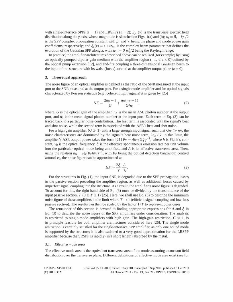
The noise figure of an optical amplifier is defined as the ratio of the SNR measured at the inputport to the SNR measured at the output port. For a single mode amplifier and for optical signalscharacterized by Poisson statistics (e.g., coherent light signals) it is given by [25]
NF =2nN +1
G+
nN(nN +1)G2n0
, (2)
where, G is the optical gain of the amplifier, nN is the mean ASE photon number at the outputport, and n0 is the mean signal photon number at the input port. Each term in Eq. (2) can betraced back to a particular noise contribution. The first term is associated with the signal’s beatand shot noise, while the second term is associated with the ASE’s beat and shot noise.
For a high gain amplifier (G � 1) with a large enough input signal such that Gn0 � nN , thenoise characteristics are dominated by the signal’s beat noise term, 2nN/G. In this limit, theamplifier’s ASE output power takes the form [21] PN = Ahν0Gξ γ−1, where h is Plank’s con-stant, ν0 is the optical frequency, ξ is the effective spontaneous emission rate per unit volumeinto the particular optical mode being amplified, and A is its effective transverse area. Then,using the relation nN = PN(Bνhν0)
−1, with Bν being the optical detection bandwidth centredaround ν0, the noise figure can be approximated as
NF ≈ 2ξγ
ABν
. (3)
For the structures in Fig. (1), the input SNR is degraded due to the SPP propagation lossesin the passive section preceding the amplifier region, as well as additional losses caused byimperfect signal coupling into the structure. As a result, the amplifier’s noise figure is degraded.To account for this, the right hand side of Eq. (3) must be divided by the transmittance of theinput passive section, T (0 ≤ T ≤ 1) [25]. Here, we shall use Eq. (3) to describe the minimumnoise figure of these amplifiers in the limit where T → 1 (efficient signal coupling and low-losspassive section). The results can then be scaled by the factor 1/T to represent other cases.
The remainder of this section is devoted to finding appropriate expressions for A and ξ inEq. (3) to describe the noise figure of the SPP amplifiers under consideration. The analysisis restricted to single-mode amplifiers with high gain. The high-gain restriction, G � 1, isin principle feasible for both amplifier architectures considered here [26]. The single moderestriction is certainly satisfied for the single-interface SPP amplifier, as only one bound modeis supported by the structure; it is also satisfied to a very good approximation for the LRSPPamplifier because the SRSPP is rapidly (in a short length) absorbed by the metal.
3.1. Effective mode area
The effective mode area is the equivalent transverse area of the mode assuming a constant fielddistribution over the transverse plane. Different definitions of effective mode area exist (see for
#151685 - $15.00 USD Received 25 Jul 2011; revised 3 Sep 2011; accepted 3 Sep 2011; published 3 Oct 2011(C) 2011 OSA 10 October 2011 / Vol. 19, No. 21 / OPTICS EXPRESS 20510

example Ref. [27] and references therein) because the choice of the constant field value is notunique. Here, we adopt the commonly used statistical measure [28]
Aι =[∫
Iι(x,y) dxdy]2∫[Iι(x,y)]
2 dxdy, (4)
where
Iι(x,y) ∝ |Ey,ι(x,y,z = 0)|2 = |Ey,ι(y)|2 exp
(− βι
zR,ιx2)
(5)
is the transverse mode intensity distribution at the output plane of the amplifier, and the integralsin Eq. (4) run over the entire (x,y) plane. Since both the single-interface SPP and the LRSPPhave a very small fraction of their fields inside the metal, one can approximate Ey,ι(y) in Eq. (5)simply by the evanescent field in the gain region(s), which upon substitution in Eq. (4) yields
Aι = ιδι
√πw2
0, (6)
with δι being the e−1 field penetration depth into the gain medium
3.2. Effective spontaneous emission rate per unit volume
We regard the gain medium as an ensemble of isotropically oriented dipoles in an excited state.Dipoles located far from the metal surface relax through spontaneous emission into bulk modes;however, those located close to the metal surface experience additional energy decay channels,such as spontaneous emission into SPPs and radiative modes of the structure, and non-radiativeenergy transfer to electron-hole pairs in the metal [29]. We are interested in the spontaneousemission into SPPs in order to describe the amplifier’s noise. To this end, we describe the ra-diative properties of individual dipoles close to the metal surface following the well-knownChance-Prock-Silbey model [22] as reformulated by Ford and Weber [23]. This aspect of thepresent theory has reproduced measured results on a LRSPP amplifier with reasonable agree-ment [21].
For a dipole located at a distance y0 from the metal surface, the spontaneous emission rateinto SPPs with arbitrary propagation directions can be written as (see Appendix A.1)
Γι(y0) = Γ0 Re∫
uιdu S(u,y0). (7)
Here, Γ0 is the dipole’s spontaneous emission rate in the bulk (no metal present), S(u,y) is thedipole’s power dissipation density normalized to its total dissipation in the bulk, and u is the in-plane wave-vector normalized to the dipole’s far-field wavenumber. The integral runs over therange of wave-vectors, uι , associated with the single-interface SPP (ι = 1) or LRSPP (ι = 2).Averaging Eq. (7) over dipole positions yields the effective spontaneous emission rate:
〈Γι〉= Γ0
ιδι
∫�g
dy Re∫
uιdu S(u,y0), (8)
where the integration range �g is taken over the entire gain medium (or media).The excited state dipole density is also a position dependent quantity, as it is inversely propor-
tional to the total spontaneous emission rate (in general it also depends on the pump intensitydistribution [29] which is assumed uniform here). It is then convenient to define an effectiveexcited state density in terms of the mode power gain coefficient as
Nι =γι +αισe(ν0)
=2β 2
g
g(ν0)Γ0π(γι +αι), (9)
#151685 - $15.00 USD Received 25 Jul 2011; revised 3 Sep 2011; accepted 3 Sep 2011; published 3 Oct 2011(C) 2011 OSA 10 October 2011 / Vol. 19, No. 21 / OPTICS EXPRESS 20511

where αι is the mode power attenuation coefficient characterizing the optical losses of thestructure (e.g., absorption in the metal, scattering loss and ground-state absorption of dipoles)such that the term (γι +αι) represents the material gain of the gain medium, σe is the dipole’semission cross-section, g(ν) is the dipole’s emission linewidth, and βg = 2π
√ε ′g/λ0 is the
wavenumber in the gain medium, with λ0 being the wavelength in vacuum. In defining Eq. (9)we have implicitly assumed that the gain medium is a four-level system and that σe is notaffected by the presence of the metal surface.
It follows that over a narrow optical bandwidth Bν centred around ν0, such that Bνg(ν) ≈Bνg(ν0), the total spontaneous emission rate per unit volume into the Gaussian SPP can bewritten as [21]
ξι = g(ν0)BνNι 〈Γι〉Fι , (10)
where Fι = θι/π is the geometrical spontaneous emission factor, with θι = 2(w0βι)−1. This
factor is included to account only for the spontaneous emission with in-plane wave-vectorsfalling within the convergence angle of the Gaussian SPP in the propagation direction [seeFig. 1(c)].
3.3. Noise figure of a high-gain SPP amplifier
An expression for the noise figure of the SPP amplifiers considered here is obtained by usingEqs. (6) to (10) into (3), yielding
NFι = 2Kιηι
∫�g
dy Re∫
uιdu S(u,y), (11)
where Kι = 4β 2g /(π3/2βι) and ηι = γι/(γι + αι) is the amplifier quantum efficiency [30],
namely, the ratio of stimulated emission not dissipated to the total stimulated emission. For theLRSPP amplifier, this equation must be solved numerically. However, for the single-interfaceSPP amplifier, one can obtain a simple analytical expression (see Appendix A.2) given by
NF1 =4
η1√
π
(ε ′m
ε ′g + ε ′m
)3/2
. (12)
In deriving this result we have assumed that |ε ′m| � |ε ′′m|, |ε ′m|> ε ′g and ε ′m < 0, which is gener-ally the case for metals at visible and near infrared wavelengths.
4. Results and discussion
In this section we use Eqs. (11) and (12) to estimate the noise figure of the two plasmonicamplifiers of interest in the high gain limit (γι � αι ), where the amplifier quantum efficiencyapproaches unity (ηι = 1). The gain media are assumed to be constituted by excited dipolesembedded in a host material of permittivity ε ′g. For the calculations we consider ε ′g = 1 (a gas),ε ′g = 2.25 (a polymer or a glass), and ε ′g = 13.8 (similar to the permittivity of a semiconductor).The metal is silver in all cases. The calculations cover wavelengths in the range 400 nm ≤λ0 ≤ 2 μm, over which the dispersion of ε ′g is neglected and εm is approximated by the Drudemodel with the parameters for silver used in Ref. [31]. Furthermore, the value of βι in Eq. (11)is calculated in the absence of gain. This is a reasonable approximation because Im(κι) isalways much smaller than Re(κι) under realistic modal gains, and hence βι is not significantlydifferent from its passive value.
#151685 - $15.00 USD Received 25 Jul 2011; revised 3 Sep 2011; accepted 3 Sep 2011; published 3 Oct 2011(C) 2011 OSA 10 October 2011 / Vol. 19, No. 21 / OPTICS EXPRESS 20512

0.4 0.6 0.8 1.0 1.2 1.4 1.6 1.8 2.02
3
4
5
6
7
8
9
0.4 0.6 0.8 1.0 1.2 1.4 1.6 1.8 2.02
3
4
5
6
0.4 0.6 0.8 1.0 1.2 1.4 1.6 1.8 2.00.01
0.1
1
0.4 0.6 0.8 1.0 1.2 1.4 1.6 1.8 2.00.1
1
10
60
NF 1
NF 2
a b
c d
Γ 2Γ 0/
Γ 1Γ 0/
εg=13.8
εg=1εg=2.25’
’
’
λ0
(μm) λ0
(μm)
λ0
(μm) λ0
(μm)
Fig. 2. High gain noise figure (a,c) and normalized spontaneous emission rates in logarith-mic scale (b,d) as a function of the wavelength, calculated for the two SPP amplifiers inFig. 1 using silver (Drude model) as the metal and three gain media exhibiting different ε ′g.The vertical dashed lines in (a,c) indicate the location of the SPP energy asymptote for thecase ε ′g = 13.8. The horizontal dashed lines in (a,c) mark the noise figure value of 4/
√π .
ηι = 1 is assumed for all calculations. NF1, 〈Γ1〉: single-interface SPP. NF2, 〈Γ2〉: LRSPP.
4.1. Single-interface SPP amplifier
As indicated previously, the noise figure of the single-interface SPP amplifier can be ob-tained numerically and analytically. Figure 2(a) shows the values of NF1 as a function of thewavelength calculated analytically using Eq. (12) (dashed curves) and by solving numericallyEq. (11) (markers). For the latter, the integration limits with respect to u are obtained as thefull-width at first minima of the pole in S(u,y) associated with the single-interface SPP. Weobserve a very good agreement between the two results.
Clearly, NF1 depends strongly on the material permittivities and operation wavelength. FromEq. (12) we note that the noise figure reaches a minimum value of NF1 = 4/
√π ≈ 2.25 when
|ε ′m| � ε ′g and η1 = 1. This is observed in Fig. 2(a), as NF1 approaches such a minimum value(indicated by the horizontal dashed line) at infrared wavelengths because ε ′m acquires a largemagnitude (∼ 100) in this range. The condition |ε ′m|� ε ′g is more demanding for a gain mediumwith a large permittivity; hence, a noise figure degradation is observed as ε ′g increases. Also,from Eq. (12) we note that NF1 = ∞ when ε ′g = ε ′m, which occurs at the energy asymptote ofthe SPP dispersion curve. This is observed in Fig. 2(a) for the case ε ′g = 13.8, as NF1 increasessharply for wavelengths approaching the energy asymptote (indicated by the vertical dashedline). A similar trend is observed at shorter wavelengths for the cases with lower ε ′g, for whichthe energy asymptote occurs at shorter wavelengths outside the simulation range.
It is worth mentioning that SPPs at wavelengths close to the energy asymptote sufferfrom extremely large propagation losses; thus, achieving a high gain with such SPPs is verychallenging.
#151685 - $15.00 USD Received 25 Jul 2011; revised 3 Sep 2011; accepted 3 Sep 2011; published 3 Oct 2011(C) 2011 OSA 10 October 2011 / Vol. 19, No. 21 / OPTICS EXPRESS 20513

0.4 0.6 0.8 1.0 1.2 1.4 1.6 1.8 2.02
2.5
3
3.5
4
0.4 0.6 0.8 1.0 1.2 1.4 1.6 1.8 2.0−15
−10
−5
0
5
10
f a , −f
b (d
B)
tm= 10 nm
15 nm20 nm25 nm30 nm
NF 2
NF1
λ0 (µm) λ
0 (µm)
a b
10 nm
tm=∞
30 nm
fa− fb
0.53 dB
Fig. 3. (a) High gain noise figure of the LRSPP amplifier as a function of the wavelengthand for several values of tm. NF1 is also shown for reference. (b) The values of fa and − fbin Eq. (13) plotted as a function of the wavelength and for several values of tm. ηι = 1 andε ′g = 2.25 are assumed for all calculations.
The noise figure degradation observed for increasing values of ε ′g and for wavelengths ap-proaching the energy asymptote follows from the Purcell effect [32], as the spontaneous emis-sion rate is enhanced due to an increased confinement of the SPP. This is shown in Fig. 2(b),which plots the normalized spontaneous emission rate into single-interface SPPs as a functionof the wavelength for the three gain media. Clearly, the rate increases with increasing ε ′g. Inparticular for ε ′g = 13.8, the spontaneous emission rate is enhanced by more than an order ofmagnitude in the visible wavelength region relative to that in the other two cases.
4.2. LRSPP amplifier
An analytical solution for Eq. (11) does not exists for the LRSPP amplifier; thus, NF2 is ob-tained by solving Eq. (11) numerically. In doing so, we calculate β2 using a transfer matrixmethod [34] and define the integration limits with respect to u as in the previous case but con-sidering the pole in S(u,y) associated with the LRSPP.
Figure 2(c) shows the calculated values of NF2 as a function of the wavelength for a silverfilm of thickness tm = 20 nm. We note that for long wavelengths, NF2 approaches the sameminimum value as that of NF1. However, in this case, the overall noise figure spectrum issignificantly improved with respect to NF1. In particular, for the two cases with smaller ε ′g,NF2 is weakly dependent on the wavelength and close to the minimum value over the visibleand infrared range. On the other hand, for ε ′g = 13.8, NF2 presents a slight increment over theinfrared region as the wavelength shortens and increases sharply for wavelengths approachingthe energy asymptote, as it was also observed for NF1. The comparatively small noise figureof the LRSPP amplifier is a direct consequence of a smaller spontaneous emission rate intoLRSPPs, as indicated by the results in Figure 2(d), which plots the normalized spontaneousemission rate into LRSPPs as a function of the wavelength for the three different gain media.
Figure 3(a) shows the computed values of NF2 for silver films with various thicknesses as-suming ε ′g = 2.25; NF1 for the same gain medium is also shown for reference. Note that NF2
increases with the film thickness because the LRSPP confinement increases, which in turn in-creases the spontaneous emission rate due to the Purcell effect. For sufficiently thick metalfilms, NF2 approaches NF1 because the LRSPP evolves into isolated single-interface SPPs oneach surface of the film. As the metal film becomes thinner, NF2 approaches the minimum valuefor all wavelengths in our calculations. Similar trends are observed for the other two gain media(not shown); however, their actual noise figure values are scaled according to Fig. 2(c).
#151685 - $15.00 USD Received 25 Jul 2011; revised 3 Sep 2011; accepted 3 Sep 2011; published 3 Oct 2011(C) 2011 OSA 10 October 2011 / Vol. 19, No. 21 / OPTICS EXPRESS 20514

4.3. Minimum noise figure
It can be shown that a high-gain Gaussian photon amplifier (i.e., a Gaussian beam propagatingthrough a bulk gain medium) with unitary amplifier quantum efficiency has a noise figure ofNF0 = 2 (3 dB), and that such a value corresponds to the theoretical minimum for high-gainphase-insensitive photon amplifiers [25]. On the other hand, the Gaussian SPP amplifiers stud-ied here have a minimum noise figure of 4/
√π (∼ 3.53 dB). To understand this difference
we consider a Gaussian photon amplifier and a Gaussian SPP amplifier, both having a uni-tary amplifier quantum efficiency, identical gain media, and the same optical bandwidth. Fromthe theory in Section 3 (with proper adaptations for the photon amplifier case) one obtains anexpression for NFι normalized to NF0, given by(
NFιNF0
)dB
=
( 〈Γι〉Γ0/2
)dB︸ ︷︷ ︸
+
(FιAιF0A0
)dB︸ ︷︷ ︸, (13)
fa fb
where (·)dB = 10log10(·); Γ0/2, A0 = w20π and F0 = (w0βg)
−2 are parameters of the Gaussianphoton amplifier, namely, the spontaneous emission rate (generated into one polarization stateonly), the effective mode area at the beam waist, and the geometrical spontaneous emissionfactor, respectively.
The first term on the right hand side of Eq. (13), fa, relates the rates of spontaneous emissionnoise (emitted in all directions) in the SPP and photon amplifiers; the second term, fb, relatestheir ability to couple such noise into the amplified mode. Figure 3(b) plots fa and − fb fordifferent values of tm assuming ε ′g = 2.25. Consider the results in the visible wavelength range.We note that when tm is very small (ι = 2), fa is also very small (〈Γ2〉 � Γ0/2) because thedensity of LRSPP modes is small; however, fb is very large (F2A2 � F0A0) because A2 → ∞ astm → 0. On the other hand, when tm = ∞ (ι = 1), fa is very large because the density of SPPmodes is large, while fb is small because the SPP is well confined, causing A1 � A0. A grad-ual transition between these two cases is observed as tm increases. Nonetheless, (NFι/NF0)dB
is always positive across the spectrum with values that depend strongly on tm at short wave-lengths and remain essentially constant (∼ 0.53 dB) at long wavelengths. From this analysis,we observe that the minimum noise figure of these Gaussian SPP amplifiers results from theinterplay between the noise generated into SPPs propagating in all directions, given by 〈Γι〉,and the coupling efficiency of such noise into the Gaussian SPP, given by the product FιAι .
It is important to mention that fa is fundamental, as it depends only on the physical propertiesof the dipole ensemble and metallic structure. This is not the case for fb, as it depends partly onthe properties of the Gaussian SPP, such as the relation between the divergence angle and thebeam waist. Thus the minimum noise figure of 4/
√π may not be a fundamental limit.
Finally, we point out that the theory presented here cannot be applied directly to a one-dimensional SPP amplifier given our use of the mode area to determine the noise photon number[nN in Eq. (2)]. Indeed, we have shown that both the mode area and the mode divergence (whichare related by a Fourier relation) play a crucial role in defining the amplifier noise figure. Weemphasize that the arrangements investigated (Fig. 1) represent physically realizable systems.
5. Summary
In summary, we have presented a theoretical analysis of noise in high-gain single-mode SPPamplifiers incorporating a dipolar gain medium. Two active plasmonic structures were exam-ined: an interface between a metal and a gain medium supporting the single-interface SPP, anda thin metal film bounded by identical gain media on both sides supporting the LRSPP. A real-istic configuration was considered where the SPP undergoing amplification has a Gaussian field
#151685 - $15.00 USD Received 25 Jul 2011; revised 3 Sep 2011; accepted 3 Sep 2011; published 3 Oct 2011(C) 2011 OSA 10 October 2011 / Vol. 19, No. 21 / OPTICS EXPRESS 20515

profile in the plane of the metal and paraxial propagation along the amplifier’s length (GaussianSPP). An expression for the noise figure was obtained in terms of the spontaneous emissionrate into the Gaussian SPP taking into account the different energy decay channels experiencedby dipoles in close proximity to the metallic surface. It was shown that the noise figure ofthese amplifiers exhibits a strong dependance on the real part of the permittivities of the metal(ε ′m) and gain medium (ε ′g) and that the figure is degraded in amplifiers with large ε ′g. From ananalytical expression derived for the noise figure of the single-interface SPP amplifier, it wasshown that the noise figure diverges at the SPP energy asymptote (ε ′m = ε ′g) and that in the high-gain limit it approaches a minimum value of 4/
√π (∼ 3.53 dB) when |ε ′m| � ε ′g. Numerical
calculations indicated that these extrema apply also to the LRSPP amplifier; however, the noisefigure in this case is significantly smaller than that of the single-interface SPP amplifier over thesame wavelength range. The origin of the minimum noise figure of these SPP amplifiers wasdiscussed, showing that it results from the interplay between the rate of spontaneous emissionnoise into SPPs and the coupling efficiency of such noise into the Gaussian SPP.
A. Appendix
A.1. Spontaneous emission rate for a dipole over a metal surface
The total power dissipated by an isotropically oriented dipole located at a distance y0 from themetal plane is given by [23]
℘(y0) = Γ0hν0Re∫ ∞
0du S(u,y0). (A.1)
whereS(u,y0) =
u
2√
1−u2
[u2R+
TM(u,y0)+(1−u2)R−TM(u,y0)+R+
TE(u,y0)]
(A.2)
is the dipoles’s power dissipation density normalized to the total power dissipated by the dipolefar away from the metal surface, with R±
TE,TM(u,y0) = 1±rTE,TM exp(i2y0βg√
1−u2), and withrTE and rTM being the Fresnel reflection coefficients for transverse-electric polarized waves(electric field parallel to the metal surface) and transverse-magnetic polarized waves (magneticfield parallel to the metal surface), respectively. The remaining parameters in Eqs. (A.1) and(A.2) are defined in the main text. The power dissipated into a particular SPP (propagating inarbitrary directions) can then be obtained by integrating Eq. (A.2) over the range of normalizedin-plane wave-vectors, uι , associated with the SPP [23]. Thus, one can represent the dipole’sspontaneous emission rate into a particular SPP (ι = 1,2) as
Γι(y0) =℘ι(y0)
hν0= Γ0Re
∫uι
du S(u,y0). (A.3)
A.2. Analytical expression for NF1
The power dissipated by an isotropically oriented dipole located at a distance y0 from the metalsurface into single-interface SPPs can be obtained analytically as [23]
℘1(y0) = Γ0hν0Re
[π(κ1/β0)
5
(ε ′g)2(−εm)1/2exp
(−2κ1y0
√−ε ′g/εm
)], (A.4)
where κ1 = β0[ε ′gεm/(ε ′g + εm)]1/2 is the SPP complex propagation constant, with β0 = 2π/λ0.
It follows from Eq. (A.3) that
Re∫
u1
du S(u,y0) =π(β1/β0)
5
(ε ′g)2(−ε ′m)1/2exp
(−2β1y0
√−ε ′g/ε ′m
)+O(ε
′′m), (A.5)
#151685 - $15.00 USD Received 25 Jul 2011; revised 3 Sep 2011; accepted 3 Sep 2011; published 3 Oct 2011(C) 2011 OSA 10 October 2011 / Vol. 19, No. 21 / OPTICS EXPRESS 20516

where β1 = β0[ε ′gε ′m/(ε ′g + ε ′m)]1/2 is the SPP phase coefficient. In deriving Eq.(A.5) we haveused a Taylor expansion to obtain the real part in Eq. (A.4), assuming that |ε ′m|� |ε ′′m|, |ε ′m|> ε ′gand ε ′m < 0, as this is generally true for metals at visible and near infrared wavelengths. Then,neglecting the term O(ε ′′
m) in Eq. (A.5) because it is small, and performing a straightforwardintegration over the space coordinate yields
∫ ∞
0dy Re
∫u1
du S(u,y)≈ λ0
4√
ε ′gε ′2m
(ε ′g + ε ′m)2 . (A.6)
Using this result and the expression for β1 into Eq. (11) yields Eq. (12).
#151685 - $15.00 USD Received 25 Jul 2011; revised 3 Sep 2011; accepted 3 Sep 2011; published 3 Oct 2011(C) 2011 OSA 10 October 2011 / Vol. 19, No. 21 / OPTICS EXPRESS 20517