Time Gain Control (Compensation) in Ultrasound Applications
13
1 SLAA724 – December 2016 Submit Documentation Feedback Copyright © 2016, Texas Instruments Incorporated Time Gain Control (Compensation) in Ultrasound Applications Application Report SLAA724 – December 2016 Time Gain Control (Compensation) in Ultrasound Applications Sanjay Pithadia, Rahul Prakash ABSTRACT This application report explains a vital functionality in Medical Ultrasound Systems called Time Gain Control or Time Gain Compensation (TGC). Starting from why TGC is important, with examples and requirements on the control signals for implementing TGC are explained in detail. The selection criteria and example circuits for external components (like Digital-to-Analog Converter (DAC) and Op-amp) are highlighted at the end. Contents 1 Introduction ................................................................................................................... 2 2 Why is Time Gain Control (TGC) Needed? .............................................................................. 3 3 How Does the Attenuator Work? .......................................................................................... 4 4 What Characteristics are Required for Control Signal for TGC? ...................................................... 6 5 Generating Control Signal for TGC Action ............................................................................... 8 6 Using Unbuffered R2R DAC ............................................................................................... 9 7 Using Current Output MDAC ............................................................................................. 10 8 Using Two MDACs ......................................................................................................... 11 9 Using High Speed DACs .................................................................................................. 11 10 Conclusion .................................................................................................................. 11 11 References .................................................................................................................. 12 List of Figures 1 Simplified Block Diagram of AFE58JD18................................................................................. 2 2 TGC for an Ultrasound Image.............................................................................................. 3 3 Typical TGC Operation at 5MHz........................................................................................... 4 4 Gain vs. Control Voltage Graph Demonstrating Linear-in-dB Attenuation Characteristic .......................... 4 5 V CNTLP and V CNTLM Configurations ........................................................................................... 5 6 Allowed Noise on the V CNTL Signal Across Frequency and Different Channels ...................................... 6 7 Filtering on V CNTLx Pins ...................................................................................................... 6 8 Control Voltage and Settling Time Relationships........................................................................ 7 9 Analog Control for TGC Operation ........................................................................................ 8 10 Using Voltage Output DAC for Generating TGC Signal ................................................................ 9 11 Using Current Output MDAC for Generating TGC Signal (Option # 1) ............................................. 10 12 Using Current Output MDAC for Generating TGC Signal (Option # 2) ............................................. 10 13 Using High Speed DAC for TGC Signal Generation .................................................................. 11 List of Tables 1 Comparison of Different Approaches for TGC Signal Generation ................................................... 11
-
Upload
khangminh22 -
Category
Documents
-
view
5 -
download
0
Transcript of Time Gain Control (Compensation) in Ultrasound Applications

1SLAA724–December 2016Submit Documentation Feedback
Copyright © 2016, Texas Instruments Incorporated
Time Gain Control (Compensation) in Ultrasound Applications
Application ReportSLAA724–December 2016
Time Gain Control (Compensation) in UltrasoundApplications
Sanjay Pithadia, Rahul Prakash
ABSTRACTThis application report explains a vital functionality in Medical Ultrasound Systems called Time GainControl or Time Gain Compensation (TGC). Starting from why TGC is important, with examples andrequirements on the control signals for implementing TGC are explained in detail. The selection criteriaand example circuits for external components (like Digital-to-Analog Converter (DAC) and Op-amp) arehighlighted at the end.
Contents1 Introduction ................................................................................................................... 22 Why is Time Gain Control (TGC) Needed? .............................................................................. 33 How Does the Attenuator Work? .......................................................................................... 44 What Characteristics are Required for Control Signal for TGC? ...................................................... 65 Generating Control Signal for TGC Action ............................................................................... 86 Using Unbuffered R2R DAC ............................................................................................... 97 Using Current Output MDAC ............................................................................................. 108 Using Two MDACs ......................................................................................................... 119 Using High Speed DACs .................................................................................................. 1110 Conclusion .................................................................................................................. 1111 References .................................................................................................................. 12
List of Figures
1 Simplified Block Diagram of AFE58JD18................................................................................. 22 TGC for an Ultrasound Image.............................................................................................. 33 Typical TGC Operation at 5MHz........................................................................................... 44 Gain vs. Control Voltage Graph Demonstrating Linear-in-dB Attenuation Characteristic .......................... 45 VCNTLP and VCNTLM Configurations ........................................................................................... 56 Allowed Noise on the VCNTL Signal Across Frequency and Different Channels...................................... 67 Filtering on VCNTLx Pins ...................................................................................................... 68 Control Voltage and Settling Time Relationships........................................................................ 79 Analog Control for TGC Operation ........................................................................................ 810 Using Voltage Output DAC for Generating TGC Signal ................................................................ 911 Using Current Output MDAC for Generating TGC Signal (Option # 1) ............................................. 1012 Using Current Output MDAC for Generating TGC Signal (Option # 2) ............................................. 1013 Using High Speed DAC for TGC Signal Generation .................................................................. 11
List of Tables
1 Comparison of Different Approaches for TGC Signal Generation ................................................... 11

SPI IN
LNA
SPI Logic
16X CLK
LNA IN
PGA24, 30 dB
16 Phases Generator
CW MixerSumming Amplifier
1X CLK
1X CLK
CW I/Q VOUT
Device (1 of 16 Channels)
ReferenceReference
DifferentialTGC VCNTL
16 x 8Crosspoint SW
SPI OUT
VCAT0 dB to -40 dB
3rd-Order LPF with 10, 15, 20,
30, 35, and 50 MHz
12-, 14-BitADC
Digital Processing(Optional)
JESD
LVDS
JESD Outputs
LVDS Outputs
Introduction www.ti.com
2 SLAA724–December 2016Submit Documentation Feedback
Copyright © 2016, Texas Instruments Incorporated
Time Gain Control (Compensation) in Ultrasound Applications
TrademarksAll trademarks are the property of their respective owners.
1 IntroductionMedical ultrasound imaging is a widely-used diagnostic technique that enables visualization of internalorgans, their size, structure, and blood flow estimation. An ultrasound system uses a focal imagingtechnique that involves time shifting, scaling, and intelligently summing the echo energy using an array oftransducers to achieve high imaging performance. The concept of focal point imaging provides the abilityto focus on a single point in the scan region. By subsequently focusing at different points, an image isassembled. When initiating an imaging, a pulse is generated and transmitted from multiple transducerelements. The pulse, now in the form of mechanical energy, propagates through the body as soundwaves, typically in the frequency range of 1 MHz to 15 MHz. The sound waves are attenuated as theytravel through the objects being imaged. Most medical ultrasound systems use the reflection imagingmode. As the signal travels, portions of the wave front energy are reflected back towards the transducer.
Signals that are reflected immediately after transmission are very strong because they are from reflectionsclose to the surface; reflections that occur long after the transmit pulse are very weak because they arereflecting from deep in the body. As a result of the limitations on the amount of energy that can be put intothe imaging object, the industry developed extremely sensitive receive electronics with wide dynamicrange. Received echoes from focal points close to the surface require little, if any, amplification. Thisregion is referred to as the near field. However, echoes received from focal points deep in the body areextremely weak and must be amplified by a factor of 100 or more. This region is referred to as the farfield. The receiver AFE has this unique challenge. It should be capable to adapt to both weak (far field)and strong (near field) received signals. This means that any strong echo must be conditioned so as to notsaturate and distort the receive chain and any weak echo must be amplified while inducing minimal noiseto determine the source of the echo. For this purpose, most of the receiver AFEs consists of:• A highly linear low noise amplifier (LNA) – whose gain is digitally programmable. Sometimes it also has
programmable input impedance for improved ultrasound probe matching characteristics• A Voltage-Controlled Attenuator (VCAT) – controlled through high bandwidth analog pins, allowing for
fast control (Note that some devices also provide digital attenuation control along with analog control.The digital control feature can eliminate the noise from the VCNTL circuit and ensure better SNR andphase noise for the TGC path. However, this document talks about the analog approach only). Thisblock is capable of increasing or decreasing the gain (linear in dB) using external signal. Typically, adifferential control structure is used to reduce common mode noise.
The function of increasing and decreasing the gain according to the linear in dB scale is termed as TimeGain Control or TGC. Figure 1 shows the simplified block diagram of Ultrasound Receiver Analog FrontEnd AFE58JD18 from Texas Instruments. It shows these blocks (in Grey color) that help in TGCfunctionality.
Figure 1. Simplified Block Diagram of AFE58JD18

www.ti.com Why is Time Gain Control (TGC) Needed?
3SLAA724–December 2016Submit Documentation Feedback
Copyright © 2016, Texas Instruments Incorporated
Time Gain Control (Compensation) in Ultrasound Applications
2 Why is Time Gain Control (TGC) Needed?Before discussing more details of how TGC is implemented, it is important to understand the function ofTGC. If an ultrasound element in the transducer is approximated as a point transmitter, then the transmitwave spreads in that area while the power density of the wave-front falls off in a classic case as inverselyproportional to the square of the distance from the transducer. Reflecting from a tissue target, the returnsignal also diminishes in the same proportions. Thus, the total round-trip spreading signal attenuationvaries as the inverse of the transducer-to-target distance to the fourth power. Body tissue reduces thesignal due to scattering and dissipation. A good rule of thumb for such attenuation is that it varies as 1dB/MHz/cm of tissue thickness. While high-frequency signals are desirable because they provide higherresolution due to their shorter wavelength, they are more rapidly attenuated - decreasing the signal-to-noise ratio of deep penetrating signals.
During an ultrasound send-receive cycle, the magnitude of reflected signal depends on the depth ofpenetration. The purpose of TGC is to normalize the signal amplitude with time; compensating for depth.When the image is displayed, similar material should have similar brightness, regardless of depth and thisis achieved by “Linear-in-dB” Gain, which means the decibel gain is a linear function of the control voltage.Figure 2 shows such an example of TGC for an Ultrasound image.
Figure 2. TGC for an Ultrasound Image

0
5
10
15
20
25
30
35
40
45
0.0 0.1 0.2 0.3 0.4 0.5 0.6 0.7 0.8 0.9 1.0 1.1 1.2 1.3 1.4 1.5Vcntl (V)
Gai
n (d
B)
Low noiseMedium powerLow power
-
ADCDynamicRange
350 mV
IOR-Level
Differential3.12VDifferential
3.5V TG
C
IOR-Level
DVGA
-32 dB20 dB
31 dB
&
38 dB
6'
ADC
Differential3.5V
How Does the Attenuator Work? www.ti.com
4 SLAA724–December 2016Submit Documentation Feedback
Copyright © 2016, Texas Instruments Incorporated
Time Gain Control (Compensation) in Ultrasound Applications
Going into more details, Figure 3 shows an example of B-mode TGC in action. As shown, a 5 MHzultrasound signal enters the LNA with 350 mVPP single ended Near Field (NF) amplitude and 3.5 VPPdifferential NF amplitude appears at the LNA output (differential gain = 20dB) where the TGC equalizesthe signal so that the ADC FS range of 3.12 VPP can be transversed to maximize the data acquisitionresolution. Note that this is just an example taken from the LM96511 Ultrasound Receive Analog FrontEnd (AFE) Data Manual (SNAS476).
Figure 3. Typical TGC Operation at 5MHz
3 How Does the Attenuator Work?Taking an example of AFE5812 from TI, the voltage-controlled attenuator is typically designed to have alinear-in-dB attenuation characteristic; that is, the average gain loss in dB (see Figure 4) is constant foreach equal increment of the control voltage (VCNTL).
Figure 4. Gain vs. Control Voltage Graph Demonstrating Linear-in-dB Attenuation Characteristic

W0004-01
(a) Single-Ended Input at VCNTLP
(b) Differential Inputs at V and VCNTLP CNTLM
TGC Gain
V = 0VCNTLM
VCNTLP
1.5V
XdB
X+40dB
TGC Gain
0V
VCNTLM
VCNTLP
XdB
X+40dB
1.5V
0.75V
www.ti.com How Does the Attenuator Work?
5SLAA724–December 2016Submit Documentation Feedback
Copyright © 2016, Texas Instruments Incorporated
Time Gain Control (Compensation) in Ultrasound Applications
The attenuator is controlled by a pair of differential control inputs, the VCNTLM and VCNTLP pins. Thedifferential control voltage spans from 0 to 1.5 V. This control voltage varies the attenuation of theattenuator based on its linear-in-dB characteristic. Its maximum attenuation (minimum channel gain)appears at VCNTLP – VCNTLM = 1.5 V and minimum attenuation (maximum channel gain) occurs at VCNTLP –VCNTLM = 0. When only single-ended CNTL signal is available, this 1.5-Vpp signal can be applied on theVCNTLP pin with the VCNTLM pin connected to ground; As Figure 5 and Figure 8 show, the TGC gain curve isinversely proportional to the VCNTLP – VCNTLM.
Figure 5. VCNTLP and VCNTLM Configurations
CVCNTL470pF
CVCNTL470pF
VCNTLP IN VCNTLP
VCNTLM
RVCNTL200
RVCNTL200
VCNTLM IN
AFE
CVCNTL470pF
CVCNTL470pF
VCNTLP IN VCNTLP
VCNTLM
RVCNTL200
RVCNTL200
VCNTLM IN
AFE
Frequency (kHz)
Noi
se (
nV/�
Hz)
1 2 3 4 5 7 10 20 30 50 100 200 500 1000 50000
1
2
3
4
5
6
7
8
9
10
D063
16 Channels32 Channels64 Channels128 Channels192 Channels
What Characteristics are Required for Control Signal for TGC? www.ti.com
6 SLAA724–December 2016Submit Documentation Feedback
Copyright © 2016, Texas Instruments Incorporated
Time Gain Control (Compensation) in Ultrasound Applications
4 What Characteristics are Required for Control Signal for TGC?The control voltage input has few characteristics that help in defining the specs for the DAC and op-ampused for generating these signals:• The control voltage input (VCNTLM and VCNTLP pins) represents a high-impedance input. The VCNTLM and
VCNTLP pins of multiple AFEs can be connected in parallel with no significant loading effects.• When the voltage level (VCNTLP – VCNTLM) is above 1.5 V or below 0 V, the attenuator continues to
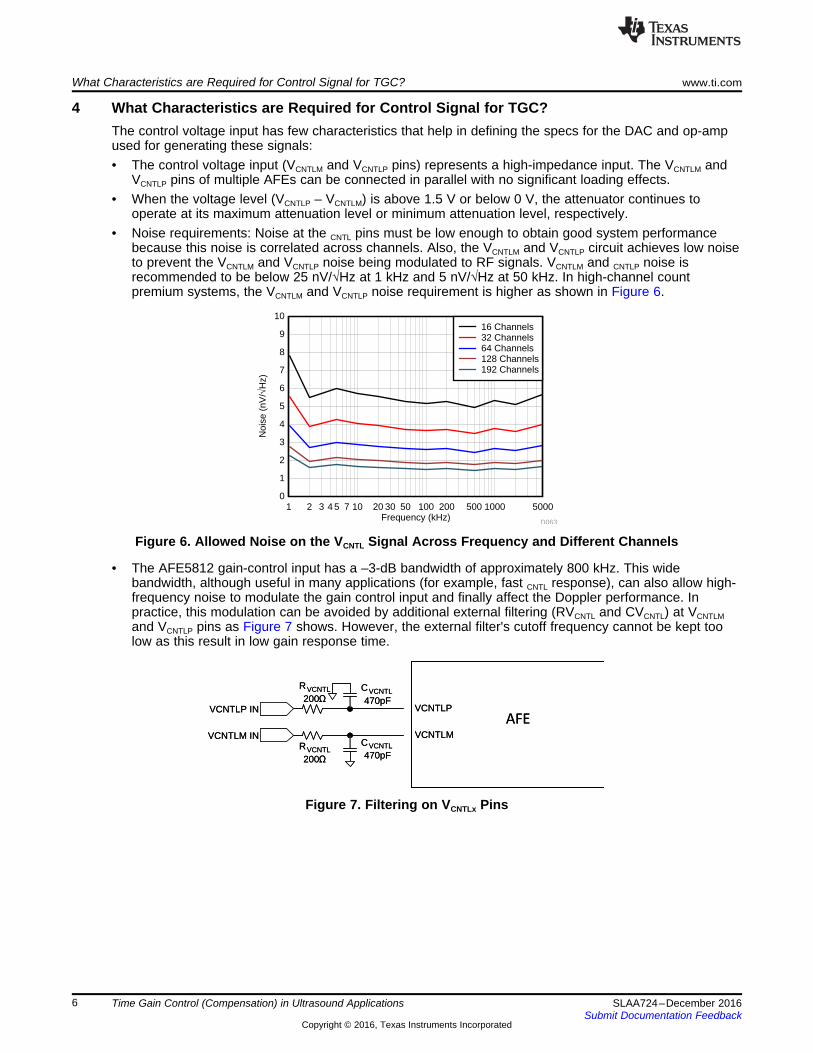
operate at its maximum attenuation level or minimum attenuation level, respectively.• Noise requirements: Noise at the CNTL pins must be low enough to obtain good system performance
because this noise is correlated across channels. Also, the VCNTLM and VCNTLP circuit achieves low noiseto prevent the VCNTLM and VCNTLP noise being modulated to RF signals. VCNTLM and CNTLP noise isrecommended to be below 25 nV/√Hz at 1 kHz and 5 nV/√Hz at 50 kHz. In high-channel countpremium systems, the VCNTLM and VCNTLP noise requirement is higher as shown in Figure 6.
Figure 6. Allowed Noise on the VCNTL Signal Across Frequency and Different Channels
• The AFE5812 gain-control input has a –3-dB bandwidth of approximately 800 kHz. This widebandwidth, although useful in many applications (for example, fast CNTL response), can also allow high-frequency noise to modulate the gain control input and finally affect the Doppler performance. Inpractice, this modulation can be avoided by additional external filtering (RVCNTL and CVCNTL) at VCNTLMand VCNTLP pins as Figure 7 shows. However, the external filter's cutoff frequency cannot be kept toolow as this result in low gain response time.
Figure 7. Filtering on VCNTLx Pins

0.0 0.2 0.5 0.8 1.0 1.2 1.5 1.8 2.0 2.2 2.50.0
2000.0
4000.0
6000.0
8000.0
10000.0
12000.0
14000.0
16000.0
18000.0
20000.0
−0.10.00.10.20.30.40.50.60.70.80.91.01.11.21.3
Time (µs)
Out
put C
ode
Vcn
tl (V
)
Output CodeVcntl
0.0 0.5 1.0 1.5 2.0 2.5 3.00.0
2000.0
4000.0
6000.0
8000.0
10000.0
12000.0
14000.0
16000.0
18000.0
20000.0
−0.10.00.10.20.30.40.50.60.70.80.91.01.11.21.3
Time (µs)
Out
put C
ode
Vcn
tl (V
)
Output CodeVcntl
www.ti.com What Characteristics are Required for Control Signal for TGC?
7SLAA724–December 2016Submit Documentation Feedback
Copyright © 2016, Texas Instruments Incorporated
Time Gain Control (Compensation) in Ultrasound Applications
• Settling time requirement: Without external filtering, the gain control response time is typically less than1 μs to settle within 10% of the final signal level of 1VPP (–6-dBFS) output as indicated in Figure 8.
Figure 8. Control Voltage and Settling Time Relationships

Generating Control Signal for TGC Action www.ti.com
8 SLAA724–December 2016Submit Documentation Feedback
Copyright © 2016, Texas Instruments Incorporated
Time Gain Control (Compensation) in Ultrasound Applications
5 Generating Control Signal for TGC ActionFor such AFEs, which support analog control for TGC operation, an external circuitry using a DAC and anop-amp is used as highlighted in Figure 9. The input signal for the DAC is fed through FPGA available onbeam forming board in ultrasound application.
Figure 9. Analog Control for TGC Operation
Based on the previous section that states some of the requirements and characteristics of control signalwaveform for TGC action, the DAC and op-amp can be selected.
For a DAC to be used in the TGC application, it should have the following specifications:• Resolution and Vref decides the DAC output voltage (Vref/2^n) - Typically 8 to 12 Bits resolution is
enough for TGC.• Channel count : 1• Settling Time : sub 1 µsec• Output Update Rate : >= 1 MSPS• Interface: The signals are coming from FPGA so in most cases DAC should support SPI interface. For
some of the high-end Ultrasound applications, LVDS or JESD supports can also be useful.
For an amplifier to be used in the TGC application, it should have the following specifications. The basicfunctionality of op-amp is to buffer and filter to suppress low frequency noise.• Should support differential or single-ended control voltage based on the requirement from AFE• Output Common-Mode voltage Control (based on requirement from AFE)• Noise requirements as per the AFE data sheet (for example AFE5812 has requirement of noise to be
below 25 nV/√Hz at 1 kHz and 5 nV/√Hz at 50 kHz)
The op-amp can be external or can be integrated into the DAC.

Unbuffered
R2R DAC
REF
DAC
Op-amp
Op-amp
0 to +VREF
SE Output
Buffer
Single-Ended to
Differential
Conversion
From
FPGA
Differential
Output
www.ti.com Using Unbuffered R2R DAC
9SLAA724–December 2016Submit Documentation Feedback
Copyright © 2016, Texas Instruments Incorporated
Time Gain Control (Compensation) in Ultrasound Applications
Given below are some examples of generating control signal for TGC action.
6 Using Unbuffered R2R DACThis approach uses a voltage output DAC having R2R architecture as shown in Figure 10. The outputvoltage has a typical requirement of low noise and fast settling, which means the output must beunbuffered and fast settling. In such scenario, a low noise external buffer must be used. The output canrange from “0 to VREF” or “-VREF to +VREF”. The unbuffered voltage output R2R DAC requires apositive reference in order to generate a positive voltage output. The reference input impedance varieswith DAC input code; hence, this topology requires reference drive circuitry to minimize the linearity errors.On the other hand, the output impedance remains constant with respect to DAC input code. This simplifiesthe output buffer design. Using this approach, the settling time is limited by compensation capacitor of theoutput buffer.
Figure 10. Using Voltage Output DAC for Generating TGC Signal

Current
Output
MDAC
REF
Op-amp
Op-amp
0 to +VREF
SE Output
I to V
Converter
Single-Ended to
Differential
Conversion
From
FPGA
Differential
OutputOp-amp
Buffer
VREF
Bias
Generation
Op-amp
Buffer
Current
Output
MDAC
REF
Op-amp
Op-amp
0 to +VREF
SE Output
I to V
Converter
Single-Ended to
Differential
Conversion
From
FPGA
Differential
OutputOp-amp
Inverting
Buffer
-VREF
Using Current Output MDAC www.ti.com
10 SLAA724–December 2016Submit Documentation Feedback
Copyright © 2016, Texas Instruments Incorporated
Time Gain Control (Compensation) in Ultrasound Applications
7 Using Current Output MDACThis method uses a current output MDAC as shown in Figure 11. The reference pin of MDAC exhibitsconstant input impedance versus input code. Therefore, this approach does not require reference drivecircuit. Additionally, faster settling time can be achieved since the MDACs outputs current instead ofvoltage. Note that the voltage on the output is inverted from the Vref pin. In order to achieve positiveoutput from this architecture, either the reference must be inverted (see Figure 11) or the Vout must beinverted using additional op-amp (see Figure 12).
Figure 11. Using Current Output MDAC for Generating TGC Signal (Option # 1)
Figure 12. Using Current Output MDAC for Generating TGC Signal (Option # 2)

www.ti.com Using Two MDACs
11SLAA724–December 2016Submit Documentation Feedback
Copyright © 2016, Texas Instruments Incorporated
Time Gain Control (Compensation) in Ultrasound Applications
8 Using Two MDACsThe previous two approaches relied on DACs to provide single ended output before converting it intodifferential output as shown in Figure 13. This approach utilizes two MDACs to generate a differentialsignal. This requires that complimentary codes need to be written to the DAC channels, for example,DAC-A to zero and DAC-B to full scale is written. This approach helps in configurability but needs twochannels of DACs, hence, increasing cost. There are DACs with dual-channel in a single chip. TheseDACs can also be used with a caution that if the write commands to the DACs are sequential; thedifferential signaling is achieved after the write to second channel of the DAC only.
9 Using High Speed DACsSome DACs that support higher speeds are available with differential output. Such DACs help ininterfacing the outputs directly (or with external differential buffer) with the AFEs. High speed DACs arealso available with LVDS and JESD interface support. The drawback of such approach is the outputvoltage noise.
Figure 13. Using High Speed DAC for TGC Signal Generation
10 ConclusionFor any ultrasound application, TGC is an important phenomenon. The ultrasound receive AFE includes avoltage-controlled attenuator for implementing TGC functionality that operates using a control voltagegenerated using external circuitry. The control voltage characteristics are used for defining the externalDAC and amplifier specifications. This application report explains the details of selecting DAC andamplifier and some approaches to use these circuits. Table 1 concludes with the pros and cons for eachapproach.
Table 1. Comparison of Different Approaches for TGC Signal Generation
Approach Pros Cons
Using unbuffered R2RDAC
Need positive reference Requires external buffer
Easier output drive Requires reference drive circuitry to minimizethe linearity errors
Simplified output buffer design because of constantoutput impedance with respect to DAC input code Higher settling time
Using current outputMDAC
No buffer required for Vref as input is impedance isfairly constant Vout is negative of reference
Faster setting time than voltage output Need to invert the referenceUsing two MDACs Configurability Two channels of DAC required
Using high speed DACs Easy interface for differential TGC signal Higher output voltage noise
References www.ti.com
12 SLAA724–December 2016Submit Documentation Feedback
Copyright © 2016, Texas Instruments Incorporated
Time Gain Control (Compensation) in Ultrasound Applications
11 References1. Texas Instruments, LM96511 Ultrasound Receive Analog Front End (AFE) Data Manual (SNAS476)2. Texas Instruments, AFE5812 Fully Integrated, 8-Channel Ultrasound Analog Front End with Passive
CW Mixer, and Digital I/Q Demodulator, 0.75 nV/rtHz, 14/12-Bit, 65 MSPS, 180 mW/CH (SLOS816)3. Texas Instruments, AFE58JD16 16-Channel Ultrasound AFE with 90-mW/Channel Power, 1-nV/√Hz
Noise, 14-Bit, 65-MSPS or 12-Bit, 80-MSPS ADC and Passive CW Mixer (SBAS737)4. TI Designs – Precision: Verified Design Single Supply Unipolar Multiplying DAC Reference Design
(TIDU300)5. TI Designs – Precision: Verified Design Voltage Mode Multiplying DAC Reference Design (TIDUAF0)6. TI Precision Designs: Verified Design ±10V 4-Quadrant Multiplying DAC (TIDU031)7. TI Designs – Precision: Verified Design Low-noise Precision Variable Reference (TIDU543)
IMPORTANT NOTICE
Texas Instruments Incorporated and its subsidiaries (TI) reserve the right to make corrections, enhancements, improvements and otherchanges to its semiconductor products and services per JESD46, latest issue, and to discontinue any product or service per JESD48, latestissue. Buyers should obtain the latest relevant information before placing orders and should verify that such information is current andcomplete. All semiconductor products (also referred to herein as “components”) are sold subject to TI’s terms and conditions of salesupplied at the time of order acknowledgment.TI warrants performance of its components to the specifications applicable at the time of sale, in accordance with the warranty in TI’s termsand conditions of sale of semiconductor products. Testing and other quality control techniques are used to the extent TI deems necessaryto support this warranty. Except where mandated by applicable law, testing of all parameters of each component is not necessarilyperformed.TI assumes no liability for applications assistance or the design of Buyers’ products. Buyers are responsible for their products andapplications using TI components. To minimize the risks associated with Buyers’ products and applications, Buyers should provideadequate design and operating safeguards.TI does not warrant or represent that any license, either express or implied, is granted under any patent right, copyright, mask work right, orother intellectual property right relating to any combination, machine, or process in which TI components or services are used. Informationpublished by TI regarding third-party products or services does not constitute a license to use such products or services or a warranty orendorsement thereof. Use of such information may require a license from a third party under the patents or other intellectual property of thethird party, or a license from TI under the patents or other intellectual property of TI.Reproduction of significant portions of TI information in TI data books or data sheets is permissible only if reproduction is without alterationand is accompanied by all associated warranties, conditions, limitations, and notices. TI is not responsible or liable for such altereddocumentation. Information of third parties may be subject to additional restrictions.Resale of TI components or services with statements different from or beyond the parameters stated by TI for that component or servicevoids all express and any implied warranties for the associated TI component or service and is an unfair and deceptive business practice.TI is not responsible or liable for any such statements.Buyer acknowledges and agrees that it is solely responsible for compliance with all legal, regulatory and safety-related requirementsconcerning its products, and any use of TI components in its applications, notwithstanding any applications-related information or supportthat may be provided by TI. Buyer represents and agrees that it has all the necessary expertise to create and implement safeguards whichanticipate dangerous consequences of failures, monitor failures and their consequences, lessen the likelihood of failures that might causeharm and take appropriate remedial actions. Buyer will fully indemnify TI and its representatives against any damages arising out of the useof any TI components in safety-critical applications.In some cases, TI components may be promoted specifically to facilitate safety-related applications. With such components, TI’s goal is tohelp enable customers to design and create their own end-product solutions that meet applicable functional safety standards andrequirements. Nonetheless, such components are subject to these terms.No TI components are authorized for use in FDA Class III (or similar life-critical medical equipment) unless authorized officers of the partieshave executed a special agreement specifically governing such use.Only those TI components which TI has specifically designated as military grade or “enhanced plastic” are designed and intended for use inmilitary/aerospace applications or environments. Buyer acknowledges and agrees that any military or aerospace use of TI componentswhich have not been so designated is solely at the Buyer's risk, and that Buyer is solely responsible for compliance with all legal andregulatory requirements in connection with such use.TI has specifically designated certain components as meeting ISO/TS16949 requirements, mainly for automotive use. In any case of use ofnon-designated products, TI will not be responsible for any failure to meet ISO/TS16949.
Products ApplicationsAudio www.ti.com/audio Automotive and Transportation www.ti.com/automotiveAmplifiers amplifier.ti.com Communications and Telecom www.ti.com/communicationsData Converters dataconverter.ti.com Computers and Peripherals www.ti.com/computersDLP® Products www.dlp.com Consumer Electronics www.ti.com/consumer-appsDSP dsp.ti.com Energy and Lighting www.ti.com/energyClocks and Timers www.ti.com/clocks Industrial www.ti.com/industrialInterface interface.ti.com Medical www.ti.com/medicalLogic logic.ti.com Security www.ti.com/securityPower Mgmt power.ti.com Space, Avionics and Defense www.ti.com/space-avionics-defenseMicrocontrollers microcontroller.ti.com Video and Imaging www.ti.com/videoRFID www.ti-rfid.comOMAP Applications Processors www.ti.com/omap TI E2E Community e2e.ti.comWireless Connectivity www.ti.com/wirelessconnectivity
Mailing Address: Texas Instruments, Post Office Box 655303, Dallas, Texas 75265Copyright © 2016, Texas Instruments Incorporated