High Gain Pattern Reconfigurable Antenna Arrays for Portable ...
134
University of South Carolina University of South Carolina Scholar Commons Scholar Commons Theses and Dissertations 2016 High Gain Pattern Reconfigurable Antenna Arrays for Portable and High Gain Pattern Reconfigurable Antenna Arrays for Portable and Body-Centric Wireless Applications Body-Centric Wireless Applications Nowrin Hasan Chamok University of South Carolina Follow this and additional works at: https://scholarcommons.sc.edu/etd Part of the Electrical and Electronics Commons Recommended Citation Recommended Citation Chamok, N. H.(2016). High Gain Pattern Reconfigurable Antenna Arrays for Portable and Body-Centric Wireless Applications. (Doctoral dissertation). Retrieved from https://scholarcommons.sc.edu/etd/3898 This Open Access Dissertation is brought to you by Scholar Commons. It has been accepted for inclusion in Theses and Dissertations by an authorized administrator of Scholar Commons. For more information, please contact [email protected].
-
Upload
khangminh22 -
Category
Documents
-
view
1 -
download
0
Transcript of High Gain Pattern Reconfigurable Antenna Arrays for Portable ...

University of South Carolina University of South Carolina
Scholar Commons Scholar Commons
Theses and Dissertations
2016
High Gain Pattern Reconfigurable Antenna Arrays for Portable and High Gain Pattern Reconfigurable Antenna Arrays for Portable and
Body-Centric Wireless Applications Body-Centric Wireless Applications
Nowrin Hasan Chamok University of South Carolina
Follow this and additional works at: https://scholarcommons.sc.edu/etd
Part of the Electrical and Electronics Commons
Recommended Citation Recommended Citation Chamok, N. H.(2016). High Gain Pattern Reconfigurable Antenna Arrays for Portable and Body-Centric Wireless Applications. (Doctoral dissertation). Retrieved from https://scholarcommons.sc.edu/etd/3898
This Open Access Dissertation is brought to you by Scholar Commons. It has been accepted for inclusion in Theses and Dissertations by an authorized administrator of Scholar Commons. For more information, please contact [email protected].

High Gain Pattern Reconfigurable Antenna Arrays for Portableand Body-Centric Wireless Applications
by
Nowrin Hasan Chamok
Bachelor of ScienceBangladesh University of Engineering and Technology, 2009
Master of EngineeringUniversity of South Carolina, 2014
Submitted in Partial Fulfillment of the Requirements
for the Degree of Doctor of Philosophy in
Electrical Engineering
College of Engineering and Computing
University of South Carolina
2016
Accepted by:
Mohammod Ali, Major Professor
Guoan Wang, Committee Member
Grigory Simin, Committee Member
Jamil A. Khan, Committee Member
Cheryl L. Addy, Vice Provost and Dean of the Graduate School

c© Copyright by Nowrin Hasan Chamok, 2016All Rights Reserved.
ii

Acknowledgments
I would like to express my deepest gratitude to my advisor Prof. Mohammod Ali for
his continuous support throughout my PhD journey. I feel absolutely privileged to
have such a mentor who has always guided me with his knowledge, time, motivation,
and philosophical advices. I am also gratefully indebted to my doctoral committee
members: Dr. Guoan Wang, Dr. Grigory Simin, and Prof. Jamil A. Khan for their
valuable comments and advices to improve this dissertation.
My cordial thanks go to my coworkers in the Microwave Engineering Laboratory:
Dr. Md. Rashidul Islam, Dr. Nazmul Alam, Paul Czeresko III, Michael Wright, and
Dhruva Paduval, for their selfless assistance and suggestions. I am thankful to our
office staff members Nat Paterson, Ashley Burt, David London, Hope Johnson, and
Alicia Williams.
I would like to extend my gratitude to my friends and members of Bangladeshi
community here, specially to Dr. Fazle Rabbi and Dr. Iftekhar Hossain, who provided
me all the supports I needed to cope with a new environment far away from home.
This dissertation would not be possible without the constant encouragement, as-
sistance, and sacrifice of my beloved wife, Firoza Binte Omar. At the time of writing
we are expecting our first baby who is already an inspiration to me!
I would like to extend my sincerest appreciation to my parents, Ahsanul Haque
and Nowrajish Ara Jahan, and my little sister, Krity Haque Charu, who have been
constant sources of encouragement throughout my life. I would also like to acknowl-
edge my grandparents and relatives in Bangladesh for their unconditional love and
caring.
iii

Abstract
Wireless devices such as smartphones, tablet computers, smartwatches etc. have be-
come ubiquitous. With that, the demand for high speed data has increased tremen-
dously. Designing antennas for such applications is challenging because of limited
availability of space, shadowing or blockage from the human body, and signal loss
from multipath fading. Conventional broad, fixed beam low gain antennas result in
poor reception, faster battery drainage, and low data rate. Compressed footprint high
gain pattern reconfigurable antenna arrays can solve these problems which is the fo-
cus of this dissertation. Two innovative high gain pattern reconfiguration techniques,
the switched beam parasitic array and the varactor controlled series-fed phased array
are studied and developed.
First, by taking advantage of the controlled coupling between closely spaced driven
and parasitic dipoles, a compressed footprint beam steering array is developed for
handheld devices. By optimizing the interelement spacing and the ON/OFF states
of the RF switches located at the input of the parasitic dipoles, beam steering in the
azimuth plane is achieved. Furthermore, a collinear arrangement of subarrays allows
narrow elevation plane beamwidth and gain of up to 11 dBi. By contrast, typical
handheld device antennas have about 3 dBi gain and little or no steering ability.
System level analysis shows about 59% improvement in signal-to-interference-plus-
noise ratio level over traditional omnidirectional antennas.
Second, a high gain switched beam parasitic array is proposed based on fabric
materials which can be integrated within the clothing or uniforms of first responders.
Material sensitivity analyses considering various conductive and nonconductive fab-
iv
rics are performed. Studies of the array near a multilayered human body phantom
reveal that a minimum distance from the body is required for the array to allow beam
steering and high gain. For example, with 10 mm spacing from the body −30 to 30
steering is achieved with 10 dBi peak gain which are excellent for high throughput
communication.
Third, a novel concept to design ultrathin directional broadband antennas using a
nonuniform aperiodic (NUA) metasurface is introduced. By employing a decreasing
taper for both the metasurface patch and their interelement spacing, broad impedance
and pattern bandwidths are attained. Experimental results show that, with a total
thickness of 0.04 free-space wavelength at the lowest frequency of operation, an oc-
tave bandwidth can be obtained, which is significantly larger compared with existing
designs on uniform mushroom electromagnetic band-gap structures. Based on the
NUA metasurface, a thin switched beam (0, 25, and 335) parasitic antenna array
is presented which with a thickness of 0.04 wavelength can attain high gain (8.4 dBi)
and very high front-to-back ratio.
Finally, to overcome the challenges of wide and overlapping beams with parasitic
arrays, and the space constraint and circuit complexity required by phased arrays, a
new varactor controlled series-fed phased array is proposed for wearable applications.
At the center of the design is a varactor controlled phase shifter, where varactor ca-
pacitance is changed by applying different bias voltages which alters the progressive
phase between series-fed antenna input currents and allows array pattern to be re-
configured. Low return loss, high gain, and beam steering with nulls between two
consecutive beams are achieved. It is observed that the choice of substrate and var-
actors are critical to minimize loss. While the works presented here reflect the 5
GHz frequency band the design and ideas are likely scalable and adaptable for next
generation mm-wave systems operating at 28, 38, and 60 GHz.
v

Table of ContentsAcknowledgments . . . . . . . . . . . . . . . . . . . . . . . . . . . . . iii
Abstract . . . . . . . . . . . . . . . . . . . . . . . . . . . . . . . . . . . iv
List of Tables . . . . . . . . . . . . . . . . . . . . . . . . . . . . . . . . ix
List of Figures . . . . . . . . . . . . . . . . . . . . . . . . . . . . . . . x
Chapter 1 Introduction . . . . . . . . . . . . . . . . . . . . . . . . . 1
1.1 Background and Motivation . . . . . . . . . . . . . . . . . . . . . . . 1
1.2 Contributions . . . . . . . . . . . . . . . . . . . . . . . . . . . . . . . 3
1.3 Outline . . . . . . . . . . . . . . . . . . . . . . . . . . . . . . . . . . . 6
Chapter 2 Beam Steering Techniques . . . . . . . . . . . . . . . . . 7
2.1 Introduction . . . . . . . . . . . . . . . . . . . . . . . . . . . . . . . . 7
2.2 Phased Arrays . . . . . . . . . . . . . . . . . . . . . . . . . . . . . . . 7
2.3 Switched Beam Parasitic Arrays . . . . . . . . . . . . . . . . . . . . . 9
2.4 Bidirectional Series-fed Phased Arrays . . . . . . . . . . . . . . . . . 11
Chapter 3 High Gain Pattern Reconfigurable MIMO AntennaArray for Wireless Handheld Terminals . . . . . . . 15
3.1 Introduction . . . . . . . . . . . . . . . . . . . . . . . . . . . . . . . . 15
3.2 Array Configuration . . . . . . . . . . . . . . . . . . . . . . . . . . . 18
vi

3.3 Modeling Details and Simulation results . . . . . . . . . . . . . . . . 20
3.4 Experimental Results . . . . . . . . . . . . . . . . . . . . . . . . . . . 28
3.5 System Level Performance Analysis . . . . . . . . . . . . . . . . . . . 33
Chapter 4 High Gain Beam Steering Arrays for WearableWireless Applications . . . . . . . . . . . . . . . . . . . 38
4.1 Introduction . . . . . . . . . . . . . . . . . . . . . . . . . . . . . . . . 38
4.2 Materials for the Proposed Wearable Antenna . . . . . . . . . . . . . 39
4.3 Proposed Array Configuration . . . . . . . . . . . . . . . . . . . . . . 41
4.4 Simulation Results . . . . . . . . . . . . . . . . . . . . . . . . . . . . 42
4.5 Experimental Results . . . . . . . . . . . . . . . . . . . . . . . . . . . 45
Chapter 5 Thin Switched Beam Parasitic Array on a Non-Uniform Aperiodic (NUA) Metasurface . . . . . . . . . 47
5.1 Introduction . . . . . . . . . . . . . . . . . . . . . . . . . . . . . . . . 47
5.2 Fat Strip Dipole Antenna on a Uniform Mushroom Type EBG . . . 51
5.3 Broadband Dipole Antenna on A NUA MetaSurface . . . . . . . . . 55
5.4 Experimental Results . . . . . . . . . . . . . . . . . . . . . . . . . . . 67
5.5 Switched Beam Array on NUA EBG Surface . . . . . . . . . . . . . . 74
Chapter 6 Low Cost Bidirectional Series-fed Phased Arrayfor Body-Centric Wireless Communications . . . . . . 80
6.1 Introduction . . . . . . . . . . . . . . . . . . . . . . . . . . . . . . . . 80
6.2 Proposed Array Configuration . . . . . . . . . . . . . . . . . . . . . . 81
6.3 Experimental Results . . . . . . . . . . . . . . . . . . . . . . . . . . . 91
vii

Chapter 7 Conclusion and Future Work . . . . . . . . . . . . . . 97
7.1 Conclusion . . . . . . . . . . . . . . . . . . . . . . . . . . . . . . . . . 97
7.2 Future Work . . . . . . . . . . . . . . . . . . . . . . . . . . . . . . . . 100
Bibliography . . . . . . . . . . . . . . . . . . . . . . . . . . . . . . . . 103
viii

List of Tables
Table 3.1 Geometry parameters for array on FR4 . . . . . . . . . . . . . . . 26
Table 3.2 Comparison of proposed array with available designs . . . . . . . . 33
Table 4.1 Dielectric properties of various non-conductive fabric materials. . . 39
Table 4.2 Electrical properties of various conductive fabrics. . . . . . . . . . 40
Table 4.3 Gain variation with different types of fabrics. . . . . . . . . . . . . 44
Table 4.4 Human tissue properties at 5 GHz. . . . . . . . . . . . . . . . . . . 44
Table 5.1 Antenna realized gain on mushroom type EBG . . . . . . . . . . . 54
Table 5.2 Patch width (in mm) and inter-element spacing (in mm). . . . . . 58
Table 5.3 Patch width (in mm) and interelement spacing (in mm) for 20%decreasing taper for different number of elements. . . . . . . . . . 58
Table 5.4 Simulated antenna realized gain and directivity on the proposedNUA metasurface . . . . . . . . . . . . . . . . . . . . . . . . . . . 66
Table 6.1 Geometry parameters for the phase shifter (in mm). . . . . . . . . 87
ix

List of Figures
Figure 2.1 Beam steering in a phased array. . . . . . . . . . . . . . . . . . . 8
Figure 2.2 Concept of array multiplication showing a single element pat-tern, the array factor, and the total array pattern (d = λ/4, β = 90). 9
Figure 2.3 Principle of a two-element Yagi-Uda array. . . . . . . . . . . . . . 10
Figure 2.4 Principle of a bidirectional series-fed phased array. . . . . . . . . 12
Figure 2.5 (a) Varactor controlled phase shifter network for series-fed arrayand (b) a single phase shifter. . . . . . . . . . . . . . . . . . . . . 13
Figure 3.1 (a) Conceptual drawings for the application domain of the pro-posed array: array at the top and side edges of the device, and(b) illustration of the working principle of the proposed patternreconfigurable array. . . . . . . . . . . . . . . . . . . . . . . . . . 17
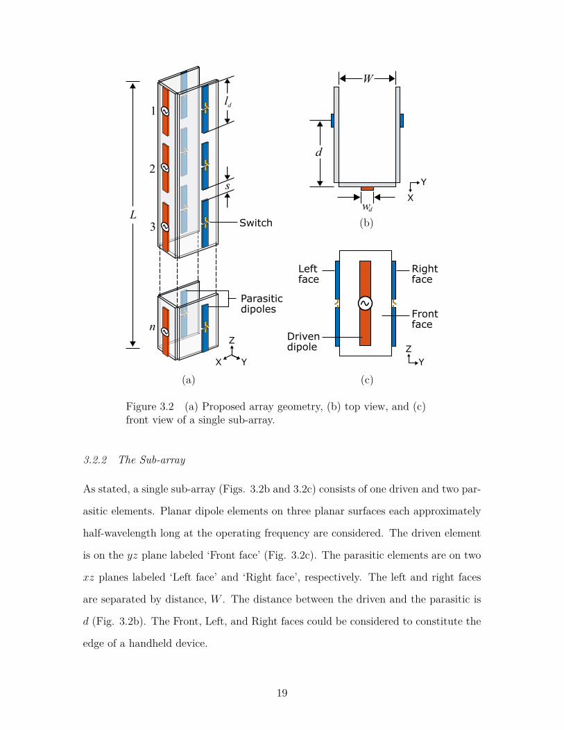
Figure 3.2 (a) Proposed array geometry, (b) top view, and (c) front viewof a single sub-array. . . . . . . . . . . . . . . . . . . . . . . . . . 19
Figure 3.3 (a) Effects on S parameter with variation of d, (b) Effects on Sparameter with variation of s when all switches are ON. . . . . . 21
Figure 3.4 Simulated S parameters vs. frequency for array in free-space . . . 23
Figure 3.5 Computed realized gain patterns in free-space in the (a) h-plane(xy) and (b) e-plane (xz). . . . . . . . . . . . . . . . . . . . . . . 24
Figure 3.6 Simulated S parameters vs. frequency for array on FR4. . . . . . 25
Figure 3.7 Computed realized gain patterns on FR4 in the (a) h-plane (xy)and (b) e-plane (xz). . . . . . . . . . . . . . . . . . . . . . . . . . 26
Figure 3.8 Configuration of the array with (a) a ground plane and (b) aground plane and a dielectric housing (not drawn to scale). . . . . 27
x

Figure 3.9 (a) Photo of the built antenna prototype (a) The array compo-nents and control circuit, (b) side-view and (c) top view of thesetup in anechoic chamber. . . . . . . . . . . . . . . . . . . . . . . 29
Figure 3.10 Selected measured S parameters vs. frequency for array on FR4. . 30
Figure 3.11 Measured realized gain patterns in the h-plane at (a) 4.8 GHz,(b) 4.9 GHz, (c) 5 GHz, (d) 5.1 GHz, (e) 5.2 GHz, and (f)measured realized gain patterns in the e-plane at 5 GHz. . . . . . 32
Figure 3.12 Envelope correlation coefficient from measured data. . . . . . . . 34
Figure 3.13 Heterogeneous Network structure with PUs, SUs, SecondaryBase Stations (SBS) within a primary cell with a Primary BaseStation (PBS). . . . . . . . . . . . . . . . . . . . . . . . . . . . . 35
Figure 3.14 Comparison of the proposed array with omni-directional an-tenna and array by Kishor and Hum. . . . . . . . . . . . . . . . . 36
Figure 3.15 Mean SINR gain of each SU. . . . . . . . . . . . . . . . . . . . . . 37
Figure 4.1 Array geometry (a) the collinear array, (b) a single sub-array,and (c) top view of the array. . . . . . . . . . . . . . . . . . . . . 41
Figure 4.2 (a) Simulated |S11| vs. frequency for different values of dx anddy, and (b) simulated |S21| vs. frequency for different values of s. 42
Figure 4.3 Comparison of S parameters vs. frequency for arrays on (a) flatsurface and (b) curvature. . . . . . . . . . . . . . . . . . . . . . . 43
Figure 4.4 (a) Top view of the array near multilayered body phantom,realized gain patterns for this set up in the (b) azimuth (XY)plane when h = 5 mm, (c) azimuth (XY) plane when h = 10mm, and (d) elevation (ZX) plane when h = 10 mm. . . . . . . . 45
Figure 4.5 Photographs of the set up for loss tangent measurement. . . . . . 46
Figure 5.1 (a) Fat strip dipole; W = 110 mm, L = 160 mm and (b) itssimulated VSWR. . . . . . . . . . . . . . . . . . . . . . . . . . . . 52
Figure 5.2 (a) A fat dipole antenna on a uniform mushroom-EBG, (b) topview, (c) simulated VSWR response. (d) simulated radiationpatterns at 450 MHz, and (e) simulated 3D pattern at 550 MHz. . 53
xi

Figure 5.3 Comparison of simulated VSWR for the EBG substrate of FR4only and a stacked substrate of FR4 and foam. . . . . . . . . . . 55
Figure 5.4 Top view of a NUA metasurface with 20% decreasing taper. . . . 58
Figure 5.5 Simulated VSWR responses for a dipole on NUA metasurfacewith different increasing taper profiles; (a) 2%, (b) 3%, (c) 4%,and (d) 5%. . . . . . . . . . . . . . . . . . . . . . . . . . . . . . . 60
Figure 5.6 Simulated impedance Vs. frequency data for dipole on NUAmetasurface with different increasing taper profiles; (a) 2%, (b)3%, (c) 4%, and (d) 5%. . . . . . . . . . . . . . . . . . . . . . . . 61
Figure 5.7 Simulated VSWR response of dipole on NUA metasurface withdifferent decreasing taper profiles; (a) 2%, (b) 4%, (c) 10%, (d)15%, (e) 20%, and (f) 20% tapering with dipole arm lengthadjusted to 120 mm each. . . . . . . . . . . . . . . . . . . . . . . 62
Figure 5.8 Simulated impedance Vs. frequency for dipole on NUA meta-surface with different decreasing taper profiles: (a) 2%, (b) 4%,(c) 10%, (d) 15%, (e)20%, (f) 20% tapering with arm length ofthe dipole adjusted to 120 mm each. . . . . . . . . . . . . . . . . 63
Figure 5.9 Simulated impedance Vs. frequency for dipole on NUA meta-surfaces with 20% decreasing taper profile. (a) arm length=156 mm, (b) arm length= 140 mm, (c) arm length= 120 mm,and (d) arm length= 100 mm. . . . . . . . . . . . . . . . . . . . . 64
Figure 5.10 Simulated realized gain patterns at (a) 319 MHz, (b) 450 MHz,(c) 550 MHz, and (d) 600 MHz. . . . . . . . . . . . . . . . . . . . 65
Figure 5.11 Simulated three dimensional realized gain patterns at (a) 319MHz, (b) 450 MHz, (c) 550 MHz, and (d) 600 MHz. . . . . . . . 66
Figure 5.12 VSWR tunability of the broadband antenna on the NUA meta-surface; h represents the height of the Antenna from the meta-surface. . . . . . . . . . . . . . . . . . . . . . . . . . . . . . . . . 67
Figure 5.13 Simulated magnetic (H) field distributions at 500 MHz on (a)conventional mushroom EBG surface and (b) NUA metasur-face. . . . . . . . . . . . . . . . . . . . . . . . . . . . . . . . . . . 68
Figure 5.14 Photographs of (a) the NUA metasurface and (b) metasurfaceplus dipole antenna. Total surface area 435 mm by 435 mm(17.1 inch by 17.1 inch). . . . . . . . . . . . . . . . . . . . . . . . 69
xii

Figure 5.15 Simulated and measured VSWR Vs. frequency of dipole onNUA- metasurface. . . . . . . . . . . . . . . . . . . . . . . . . . 70
Figure 5.16 Measured normalized E-plane radiation patterns. . . . . . . . . . 71
Figure 5.17 Measured normalized H-plane radiation patterns. . . . . . . . . . 72
Figure 5.18 Measured dipole broadside realized gain vs. frequency on theNUA metasurface. . . . . . . . . . . . . . . . . . . . . . . . . . . 73
Figure 5.19 Measured dipole patterns at other frequencies (on NUA- meta-surface). . . . . . . . . . . . . . . . . . . . . . . . . . . . . . . . 74
Figure 5.20 Measured dipole broadside realized gain vs. frequency on theNUA metasurface. . . . . . . . . . . . . . . . . . . . . . . . . . . 75
Figure 5.21 (a)Top view of a uniform EBG, (b) |S11| Vs. frequency, and (c)azimuth plane (xy) pattern. . . . . . . . . . . . . . . . . . . . . . 77
Figure 5.22 (a)Top view of a NUA EBG, (b) |S11| Vs. frequency, and (c)azimuth plane (xy) pattern. . . . . . . . . . . . . . . . . . . . . . 78
Figure 6.1 Array geometry (a) the collinear array, (b) a single sub-array,and (c) top view of the array. . . . . . . . . . . . . . . . . . . . . 81
Figure 6.2 (a) Configuration of a single sub array, (b) dimensions of asingle driven dipole, (c) dimensions of a parasitic element, (d)|S11| vs. frequency for the single subarray and (e) Realized gainpattern in the yz plane at 5.2 GHz. . . . . . . . . . . . . . . . . . 83
Figure 6.3 (a) Cross-sectional view (yz plane) of the array, (b) Snn vs.frequency, and (c) realized gain pattern in yz plane at 5.2 GHzfor three progressive phases. . . . . . . . . . . . . . . . . . . . . . 84
Figure 6.4 (a) Geometry of a single phase shifter and (b) an unequal lengthbranchline coupler. . . . . . . . . . . . . . . . . . . . . . . . . . . 86
Figure 6.5 (a) S11 vs. frequency, (b) S21 vs. frequency, and (c) S11 phasevs. frequency for different capacitance values. . . . . . . . . . . . 87
Figure 6.6 (a) S11 vs. frequency when the array was fed from Left side. (b)Realized gain patterns in the yz plane at 5.2 GHz for C = 0.6pF and C = 2.2 pF, and (c) Realized gain patterns in the yzplane at 5.2 GHz for C = 1 pF. . . . . . . . . . . . . . . . . . . . 89
xiii

Figure 6.7 Simulation results for array on fabric substrate. . . . . . . . . . . 90
Figure 6.8 (a) Photograph of a fabricated phase shifter and (b) phaseshifter measurement set up. . . . . . . . . . . . . . . . . . . . . . 91
Figure 6.9 (a) Photograph of a fabricated phase shifter, (b) measured S11,(c) measured S21, and (d) measured S21 phase of the shifter. . . . 93
Figure 6.10 Photograph of the (a)top layer of the array with parasitic ele-ments and (b) bottom later of the array containing the phaseshifter network, and (c) measured |S11| vs. frequency for twodifferent bias voltages. . . . . . . . . . . . . . . . . . . . . . . . . 95
xiv

Chapter 1
Introduction
1.1 Background and Motivation
For over four decades there have been tremendous growth and proliferation in wireless
communication technology as evident from applications such as voice, video stream-
ing, and online games. Wireless devices such as mobile phones, wireless enabled
computers and laptops, and GPS terminals have become ubiquitous. Lately even
wearable wireless devices such as smart glasses, smart watches, and smart sensors
have begun to being adopted and used. It is estimated that by 2020 around 50 bil-
lion devices will be connected with the wireless network [1]. With these growths the
demand for higher data rates has also grown significantly. For example, the first
generation (1G) communication systems offered about 14 kilobits per second (kbps)
of data rate. Present day WiFi, WiMAX and 4th Generation Long Term Evolution
(LTE) uses up to 1 Gbps of data rate. Looking beyond, data rates of 10 Gbps are
quite feasible.
To meet future demands of ever increasing data rates, innovative new antennas
must be designed that can offer higher gain within a very small form factor. This
applies to both handheld and wearable wireless applications. That is the focus of this
dissertation.
Traditional antennas that are frequently used in handheld devices are fixed beam
antennas such as Planar-Inverted F Antennas (PIFAs) [2–4], slots [5–8], patches [9–
14], monopoles, [15–19] and loops. [20–22]. Similarly for wearable applications most
1

commonly used antennas are patch antennas [23–30], PIFAs [31–34], wire antennas
[35–43], EBG based antennas [44–51] etc. These antennas are inefficient and hence
offer low gain. Furthermore, they lack steering capabilities which are critical for
higher capacity. Although diversity [52–59] addresses some of these concerns, it is
not an alternative against high-gain beam steering antennas. Even with diversity,
devices often suffer from poor reception, which eventually causes the battery to drain
very fast. This occurs because when the link margin is weak the transmitter transmits
at the highest power level to compensate for that, e.g. 1 bar vs. 5 bars on one’s phone
screen.
High gain beam steering arrays offer three important benefits [60]:
(i) Spatial Filtering: Beam steering arrays can suppress the signal coming from
undesired directions. It is reported that beam steering arrays can alleviate problems
of multipath fading [61] which occurs when signals from a source travel along multiple
paths and are incident upon the receiver containing different phases that represent
each individual path. Targeting the beam along a single path can greatly reduce the
deleterious multipath fading effect.
(ii) Link Margin Enhancement: Arrays due to their high-gain and narrow beamwidth
can either increase the communication distance or increase the data rate when the
distance is the same.
(iii) Sensitivity Improvement: It has been shown that for an array with n- driven
elements, the total received signal power is n2 times stronger than the signal from a
single source, whereas the noise power gets amplified by n. Consequently, the Signal-
to-Noise Ratio (SNR) increases n times. This allows for higher data rate as SNR is
directly related to the maximum data rate or the data capacity, C of a communication
channel by Shannon’s formula,
C = B log2(1 + SNR) (1.1)
where B is the bandwidth of the channel.
2

Various techniques exist to design and develop high gain beam steering antenna
arrays. These include Phased array, Electronically Steerable Parasitic Array Radiator
(ESPAR), Frequency scanning array etc. An overview of the most relevant techniques
and how they relate to the proposed dissertation work is given in Chapter 2.
Notwithstanding, the focus of this dissertation is to develop innovative new an-
tenna concepts that are suitable for handheld and wearable wireless device applica-
tions. Key metrics are high-gain, steerable beam and smaller form factors.
1.2 Contributions
In this dissertation, several innovative methods and techniques to design and develop
high-gain beam steering antenna arrays are presented that are suitable for handheld
and wearable wireless applications.
First, we introduce the idea of a compressed footprint high gain beam steer-
ing collinear antenna array for handheld devices [62–64]. To our knowledge, this is
the first ever documented compressed footprint high gain beam steering array for
a handheld device. The array design is focused on the 5 GHz frequency band; it is
understood that translating such a design at higher frequencies will be fairly straight-
forward. The collinear array is formed using n subarrays. Each subarray containing
one driven dipole and two parasitic strip dipoles the latter of which are controlled
using integrated RF switches at their centers. For each subarray, when the driven
element is excited, currents are induced into the two parasitic elements the magni-
tude and phase of which depend on the interelement distances, the switch equivalent
circuit parameters (ON vs OFF), and the antenna size and geometrical parameters.
These parameters have significant effects on both the driving point impedance of the
driven element as well as the array factor that determines the beam direction and
gain. Analysis efforts are directed to optimize these parameters which allow good
driving point impedance, high gain, and beam steering in the azimuthal plane with
3
a small form factor suitable for handheld devices. High gain is achieved by forming a
collinear array which allows significant reduction in the elevation plane beamwidth.
A design example on low cost FR4 substrate is presented and its efficacy for practical
MIMO application scenario is evaluated on a system level simulation testbed. An
experimental prototype of the proposed array is fabricated and tested that consist of
PIN diode switches. The fabricated prototype demonstrates performance as expected
with some minor discrepancies e.g. irregular nulls in radiation patterns, gain reduc-
tion and a minor shift in frequency of operation. The reasons for these discrepancies
can be attributed to the effects of long DC bias wires and the use of coaxial baluns.
Second, we investigate and design a high gain beam steering parasitic antenna
array for wearable application platforms [65, 66]. This is also a collinear array of
n subarrays, where the subarray consists of one driven and two parasitic dipole ar-
rays. The basic principle of operation for this array is similar to the collinear array
operation presented above with the exception that the array design must consider
wearable materials (conductive and non-conductive fabrics) and the presence of the
human body near the antenna array. Also to make it suitable for wearable applica-
tions the antenna array must be thin enough for integration into the garment which
necessitated the study and design of V-dipoles instead of straight dipoles before.
Based on literature reviews several conductive and non-conductive fabric substrates
are considered to fabricate the array. Antenna array design is performed considering
layers of fabric materials that can be used to build the array. The effects of human
body near the antenna array are analyzed.
Third, a new technique to design ultra-thin directional broadband antennas using
a Non-Uniform Aperiodic (NUA) metasurface is introduced. Study and design of the
NUA metasurface show that by employing a decreasing taper for both the metasurface
patch and their interelement spacing broad impedance and pattern bandwidths can
be attained [67–69]. Experimental results show that with a total thickness of 0.04
4

of the free space wavelength (corresponding to the lowest frequency of operation) an
octave bandwidth can be attained which is significantly larger compared to existing
designs on uniform mushroom EBG (Electromagnetic Band Gap) structures. The
concept of NUA EBG surface is then exploited to develop a thin beam switched
parasitic array for 2.4 GHz wireless application [70].
Finally, we present a bidirectional series-fed phased array for body-wearable wire-
less applications. The beam switched parasitic arrays discussed above have a common
disadvantage, their azimuthal beamwidth is wide and no reasonable null exists be-
tween the different states of the beams. As conventional phased arrays are incompat-
ible in wearable applications for their high cost and complexity we propose to design
and develop a varactor controlled series-fed bi-directional phased array antenna. As a
viable alternative for wearable applications, series-fed varactor controlled microstrip
patch antennas have been proposed for base station application by others [71]. Our
objective is to study and design such arrays for wearable applications considering
dipole antennas made from textile materials. The use of dipoles makes the array
footprint sparse. Moreover, the use of textile materials studied in the work presented
above allows us to leverage that knowledge to develop narrow beam high gain beam
steering arrays. The series-fed array consists of several dipoles that are excited using
pairs of varactors that are connected to branchline couplers. By changing the bias
of the varactors the phase shift is controlled which allows beam steering at -25, 25
etc. degrees. It is critical that impedance matching, gain, and pattern steering is
achieved simultaneously as the varactor states are changed. Preliminary design op-
timizations have been performed. Laboratory prototypes of a single phase shifter on
FR4 substrate and a series fed array on TMM4 substrate were fabricated and mea-
sured for S-parameters by applying different bias voltages. The measurement results
show reasonable response with minor aberrations such as slightly high insertion loss
and minor shift in frequency of operation, which can be attributed to imperfections
5

in fabrication process, dielectric loss from substrate loss, and insertion loss due to
parasitic series resistance in the varactor diodes.
1.3 Outline
This dissertation is organized as follows. Chapter 2 describes three important beam
steering techniques and their applicability for portable and wearable devices. In
Chapter 3, the design and development of a high gain beam steering collinear MIMO
array for portable handheld devices are presented. Significant performance parame-
ters such as the return loss, isolation, bandwidth, peak beam directions, realized gain,
envelope correlation coefficient are investigated. In a realistic communication envi-
ronment, the system level improvement in Signal-to-Noise ratio due to the antenna
array is showed. Chapter 4 presents a thin switched beam parasitic MIMO array for
wearable applications. The challenges for designing antenna arrays for body-centric
applications are specified. Several characteristics of the array such as return loss,
mutual coupling, beam scanning, bandwidth, gain are studied. In Chapter 5, we
introduce the concept of a novel broadband non uniform aperiodic EBG metasurface.
Based on that design a thin beam switched parasitic array is developed. In Chapter
6, a novel bidirectional series-fed phased array for body-centric wireless application
is introduced. Experimental data of S-parameter magnitude and phases for a single
phase shifter from the array is presented. Chapter 7 concludes this dissertation with
directions for future works.
6

Chapter 2
Beam Steering Techniques
2.1 Introduction
Beam steering here means electronic steering where certain electronic devices or cir-
cuits are used to steer the beam of an array in space. important parameters may
include gain, beamwidth, beam direction, Forward to Backward ratio, Side Lobe
Level (SLL) etc. In general, beam steering can be obtained using phased arrays,
switched beam parasitic arrays, frequency scanning arrays etc. Each of these ap-
proaches has its own merits and demerits and are thus suitable for certain classes
of applications. For portable and wearable applications, phased arrays and switched
beam parasitic arrays are preferred. Basic principles of these two types of arrays are
described below.
2.2 Phased Arrays
Phased arrays are widely used to electronically steer the beam of an array in a desired
direction while suppressing the beam in other directions. This requires carefully
controlling the phase of the individual element of an array.
Consider a linear array consisting of n identical isotropic radiators arranged along
the z axis (Fig. 2.1). Each element is excited with a uniform current with magnitude,
I0 and progressive phase shift, β. The spacing between any two consecutive elements
is d. The array factor for such an array is given by [72],
AF = 1 + ej(kd cos θ+β) + ej2(kd cos θ+β) + . . .+ ej(n−1)(kd cos θ+β). (2.1)
7

The normalized array factor can be written as
(AF )n ∼=sin Nψ
2Nψ
2(2.2)
where ψ = 2πdλ
cos θ + β, with k = 2π/λ.
The maximum occurs at ψ = 0 which gives us the angle where the beam peak
occurs,
θm = cos−1 λβ
2πd. (2.3)
This is an important relation that will be referred to in our future discussions.
Equation (2.3) clearly defines the beam direction as function of λ, β, and d. For
example if n = 15, d = λ/2, and β = 0, the array beam is directed along θm = 90,
while for β = 90 the array beam is directed along θm = 60 (see Fig. 2.1).
X
Z
Isotropic elementd
X
Z
Figure 2.1 Beam steering in a phased array.
With regard to an actual array consisting of real elements such as, dipoles, patches
etc. the total field, E(total) of an array is found by multiplying the array factor (AF)
with the pattern of the element as defined in (2.4)
E(total) = Element Factor× Array Factor. (2.4)
For example, the total field pattern of a two element array of infinitesimal dipoles
at d = λ/4 with β = 90 is shown in Fig. 2.2.
8

1
0.75
0.50
0.25
1
0.75
0.50
0.25
1
0.75
0.50
0.25
θ θ θ θ θ θ
Figure 2.2 Concept of array multiplication showing a single element pattern, thearray factor, and the total array pattern (d = λ/4, β = 90).
Although phased arrays provide tremendous opportunities to obtain beam direc-
tion, width, SLL, F/B etc. These come at a higher cost and are hence not preferred
for small handheld devices. The primary disadvantage of d = λ/2 precludes applica-
tions below 5 GHz. Other disadvantages are that they need costly and complicated
phase shifters. For example, cost of a phased array used in collision avoidance radars
in high-end vehicles could be between $1500 - $3000.
2.3 Switched Beam Parasitic Arrays
Switched beam parasitic arrays can possibly be best understood from Yagi-Uda arrays
[73, 74]. A typical Yagi-Uda consists of a driven dipole, a shorted parasitic dipole
that acts as a reflector and multiple shorted parasitic dipoles that act as directors.
Such an array generates an endfire beam going in the direction of the directors.
The theoretical understanding of a Yagi-Uda array can be based on the concept of
reactively controlled directive arrays proposed by Harrington [75] where he used a
more general approach and considered the parasitic elements to be terminated using
variable reactance. Later Kawakami and Ohira [76] used the same concept to develop
Electronically Steered Parasitic Array Radiators (ESPAR).
The principle is illustrated in Fig. 2.3. As seen, two dipole elements are placed
9
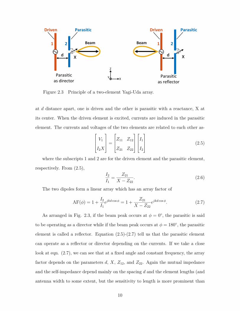
Figure 2.3 Principle of a two-element Yagi-Uda array.
at d distance apart, one is driven and the other is parasitic with a reactance, X at
its center. When the driven element is excited, currents are induced in the parasitic
element. The currents and voltages of the two elements are related to each other as- V1
I2X
=
Z11 Z12
Z21 Z22
I1
I2
(2.5)
where the subscripts 1 and 2 are for the driven element and the parasitic element,
respectively. From (2.5),I2
I1= Z21
X − Z22. (2.6)
The two dipoles form a linear array which has an array factor of
AF(φ) = 1 + I2
I1ejkd cosφ = 1 + Z21
X − Z22ejkd cosφ. (2.7)
As arranged in Fig. 2.3, if the beam peak occurs at φ = 0, the parasitic is said
to be operating as a director while if the beam peak occurs at φ = 180, the parasitic
element is called a reflector. Equation (2.5)-(2.7) tell us that the parasitic element
can operate as a reflector or director depending on the currents. If we take a close
look at eqn. (2.7), we can see that at a fixed angle and constant frequency, the array
factor depends on the parameters d, X, Z12, and Z22. Again the mutual impedance
and the self-impedance depend mainly on the spacing d and the element lengths (and
antenna width to some extent, but the sensitivity to length is more prominent than
10

the width). So, d, X, and antenna lengths are the key variables for this type of array.
For dipole elements antenna lengths are often close to a half wavelength, leaving only
the spacing (d) and variable reactance (X) as the key contributors.
(a) Effect of d: When d is small, Z2 and Z1 are large. This makes the driving point
impedance, Zd small. That results in poor S11 when the driven antenna is excited
with a 50 Ω feed,
|S11| =∣∣∣∣Zd − Z0
Zd + Z0
∣∣∣∣ (2.8)
where Z0 is the characteristic impedance of the feed line (50 Ω).
Again, if d is very large, the induced current is very weak and that results in poor
array factor.
(b) Implementing X: The variable reactance, X can be implemented using semi-
conductor devices, such as PIN diodes, Field Effect Transistors, and RF MEMS
switches. Varactor diodes can also be used to obtain more precise control over a
range of reactances.
Switched beam parasitic arrays occupy less space because d λ. Also since they
do not require external phase shifters the cost is low. These advantages make such
array suitable for portable handheld devices and wearable applications. Drawbacks
include its relatively wide beamwidth (∼ 90 to ∼ 120) and overlapping beams.
2.4 Bidirectional Series-fed Phased Arrays
To avoid the complexity of traditional phased arrays, a new series-fed phased array
was proposed by Ehyaie [60]. It is a bidirectional array. As shown in Fig. 2.4 each
of the two terminal ports in the series-fed array can be reconfigured as either a load
or an input with the help of a matched Double-Pole-Double-Throw (DPDT) switch.
Using this method, the same value of a variable reactance can be used twice (for two
11
Fed from left
Switch
Pattern
Antenna element
Phase shifter
θ -θ
Fed from right
Figure 2.4 Principle of a bidirectional series-fed phased array.
feeding configurations) to steer the beam in two different directions, reducing the
phase-shifter complexity by half.
To understand the principle let us rearrange Equation (2.3), assuming the elements
are placed along the y axis, and the steering plane being the yz plane,
θm = sin−1 −λβ2πd . (2.9)
Let us consider that the array elements are λ/2 apart. If the phase shifters provide
a progressive phase shift ranging from 0 to β, the array peak beam direction can
be steered from 0 to θ = − sin−1 βπ. When the feed direction is switched, the phase
shifters provide a progressive phase shift ranging from 0 to −β causing the array peak
beam direction to steer from 0 to −θ = sin−1 βπ. Therefore, total of 2 sin−1 β
πsteering
can be made possible.
The phase shift required can be achieved using varactor diodes. An example is
shown in Fig. 2.5a which consists of delay lines, unequal-line length couplers, varactor
diodes and grounded radial stubs.
The principle can be understood by analyzing a single phase shifter such as the one
shown in Fig. 2.5b. When different bias voltages are applied, varactor capacitances
12
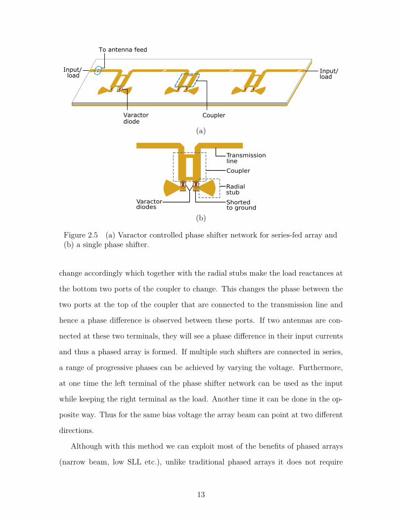
loadInput/
To antenna feed
Varactordiode
Coupler
loadInput/
(a)
Coupler
Shorted
Radial
Varactorto grounddiodes
Transmission
stub
line
(b)
Figure 2.5 (a) Varactor controlled phase shifter network for series-fed array and(b) a single phase shifter.
change accordingly which together with the radial stubs make the load reactances at
the bottom two ports of the coupler to change. This changes the phase between the
two ports at the top of the coupler that are connected to the transmission line and
hence a phase difference is observed between these ports. If two antennas are con-
nected at these two terminals, they will see a phase difference in their input currents
and thus a phased array is formed. If multiple such shifters are connected in series,
a range of progressive phases can be achieved by varying the voltage. Furthermore,
at one time the left terminal of the phase shifter network can be used as the input
while keeping the right terminal as the load. Another time it can be done in the op-
posite way. Thus for the same bias voltage the array beam can point at two different
directions.
Although with this method we can exploit most of the benefits of phased arrays
(narrow beam, low SLL etc.), unlike traditional phased arrays it does not require
13

long delay lines with numerous RF switches, which makes it low-cost. This technique
can be utilized to develop wearable antenna arrays, where space is available. For
high frequency applications such as massive MIMO, mm-wave communications, this
technique can be implemented in portable handheld devices also.
14

Chapter 3
High Gain Pattern Reconfigurable MIMO
Antenna Array for Wireless Handheld
Terminals
3.1 Introduction
Multiple-input multiple-output (MIMO) wireless systems are defined as systems that
comprise multiple antenna elements at both the transmitter and receiver ends [77].
MIMO offers important advantages over conventional antennas both in terms of data
reliability and data capacity [78]. Considered as one of the most promising candidates
of future smart antenna systems, MIMO has already been adopted for IEEE 802.11n
[79], worldwide interoperability for microwave access (WiMAX) [80, 81] and long term
evolution (LTE) [82].
MIMO for handhelds is an important research area that has the potentials to
bring significant advances on antenna and antenna array designs that can be housed
within the smaller form factor of a mobile handheld terminal, such as a smartphone
or a tablet (iPad). Traditional antennas that are frequently used in handheld devices
are fixed beam antennas such as Planar-Inverted F Antennas (PIFAs) [4, 83–86] and
monopole antennas [15, 87, 88].
These are inefficient antennas because due to low antenna gain and lack of pattern
reconfiguration capability much of the radiated RF power is absorbed by the head
or the body resulting in wasted battery power. Furthermore, losses due to multipath
15

fading result in signal degradation or loss. To circumvent the fading problem diversity
[52, 56, 58, 59] have been proposed. Research has shown that only using diversity
in a handheld unit signal-to-noise ratio (SNR) improvement of over 8-10 dB can be
achieved [56]. This increase in SNR in turn decreases the bit-error-rate [89] resulting
in improved spectral efficiency.
MIMO for the handheld [90–92] offers great deal of flexibility especially if it can
be combined with high gain and pattern reconfiguration. Other MIMO Antenna
examples include [93–95]
The focus of this chapter is to introduce a smaller form factor high gain pattern
reconfigurable MIMO antenna array for handheld terminals. The array is designed
and developed using the concept of parasitic arrays [96–103] where a driven and one
or more closely coupled parasitic elements work in tandem to allow pattern reconfig-
uration. Since the parasitic elements can be brought very close to the driven antenna
element the form factor of the array will be much smaller compared to a traditional
phased array making them more suitable for handheld device applications. Although
many articles have been published in the literature on parasitic arrays that address
dipole or monopole antennas for base stations [97, 98], patch antenna arrays [99, 100],
and dipole antenna arrays for wearable wireless applications [31-33], this is the first
ever reported detailed work on a high gain pattern reconfigurable collinear parasitic
array for the handheld to our knowledge. Very preliminary results of this work were
presented at a conference recently [62]. This chapter presents more significant design,
analysis, and experimental results and system level simulation results.
The application domain for the proposed array is illustrated in Fig. 3.1a. It
is a collinear array of dipole antennas arranged at one edge of a handheld terminal.
Although proposed here for handheld terminal the concept is valid for many other ap-
plications. The proposed antenna array offers two important features: it can steer the
beam in three different directions, and has high gain with narrow e-plane beamwidth.
16

High gain is achieved by employing the collinear array geometry consisting of multiple
‘sub-arrays’ that allow narrow e-plane beamwidth.
0°70°
290°
BeamArray
Device
300°330° 0° 30°
60°
Parasiticreflector
Drivenelement
Switch
(a) (b)
Figure 3.1 (a) Conceptual drawings for the application domain ofthe proposed array: array at the top and side edges of the device,and (b) illustration of the working principle of the proposed patternreconfigurable array.
Pattern reconfiguration on the other hand, is achieved with the help of the para-
sitic array idea which can be explained with the help of one sub-array. Each sub-array
contains three dipole elements - one driven and two parasitic (Fig. 3.1b). The para-
sitic dipoles function as reflectors once activated using RF switches that are located
at their centers. This allows array pattern reconfiguration in three different directions
for three cases. For example, when switch 1 is ON, the parasitic on the left works as
a reflector making the beam point at φ = 70, when switch 2 is ON, the parasitic on
the right works as a reflector making the beam point at φ = 290, and when both
switches 1 and 2 are ON, both parasitics work as reflectors and the beam points at
φ = 0.
The operating frequency considered here is the 5 GHz WLAN band. The rapid
17

growth and interest in mm wave frequencies and massive MIMO will allow much larger
arrays to be implemented using this concept in a variety of application scenarios, e.g.
handhelds and base stations, stationary device to device, and chip to chip in computer
systems.
The chapter is organized as follows. First, the array configuration parameters are
defined. Preliminary simulation studies are performed considering the array imple-
mentation in free-space where the effects of parameters, such as, the interelement
distances and spacing between subarrays on array input return loss and mutual cou-
pling are investigated. Upon selection of appropriate design parameters, array models
with implementation scopes in free-space and on FR4 substrates are developed and
analyzed both in terms of S-parameters and radiation patterns. Next, measured S-
parameter results and radiation pattern characteristics of the array are presented
followed by system level simulations demonstrating performance under communica-
tion scenarios.
3.2 Array Configuration
3.2.1 The Collinear Array
The geometry and dimensions of the proposed array are shown in Fig. 3.2a. There
are n sub-arrays with the edge to edge separation between two consecutive sub-arrays
being s. The length of the array is L. The array axis is the z axis for our analysis
with the beam pointing orthogonal to the axis. With increasing n or s, the e-plane
beamwidth decreases resulting in increased directivity. The choice of n and s is
determined primarily by the space available in terms of the operating wavelength.
The parameter, s is also critical as it governs the coupling between two consecutive
sub-arrays.
18
1
2
3
n
L
ld
s
Switch
X
Y
ZY
Parasiticdipoles
Drivendipole
Z
YX
Leftface
Rightface
Frontface
W
d
wd
Figure 3.2 (a) Proposed array geometry, (b) top view, and (c)front view of a single sub-array.
3.2.2 The Sub-array
As stated, a single sub-array (Figs. 3.2b and 3.2c) consists of one driven and two par-
asitic elements. Planar dipole elements on three planar surfaces each approximately
half-wavelength long at the operating frequency are considered. The driven element
is on the yz plane labeled ‘Front face’ (Fig. 3.2c). The parasitic elements are on two
xz planes labeled ‘Left face’ and ‘Right face’, respectively. The left and right faces
are separated by distance, W . The distance between the driven and the parasitic is
d (Fig. 3.2b). The Front, Left, and Right faces could be considered to constitute the
edge of a handheld device.
19

3.2.3 The Operation of the Sub-array
The driven element is fed using a 50Ω source at its center. The parasitic elements
contain RF switches at their centers. Consider the operation of one of the parasitic
elements. With the switch OFF each piece of the parasitic is electrically too small
to have any effect on the antenna. With the switch ON currents are induced in
the parasitic. Following [103], the voltages and currents in the driven and parasitic
elements are related by the impedance (Z) matrix given in V1
I2X
=
Z11 Z12
Z21 Z22
I1
I2
(3.1)
and
α21 = I2
I1= −Z21
Z22 −X(3.2)
where the subscripts 1 and 2 correspond to the driven element and the parasitic
element, respectively. The parameters ZNN and the ZMN are the self and mutual
impedances in the Z matrix. The excitation voltage in the driven element is V1.
Clearly ZMN will strongly depend on the distance, d (Fig. 3.2b). Once the Z matrix
is calculated Equation (3.2) should be used to determine the magnitude and phase of
the coupling coefficient, α21. The phase angle of (3.2) determines if a certain parasitic
element will act as a reflector or director; reflector if phase is positive and director if
phase is negative [101]. If the parasitic elements are controlled using RF switches or
varactor didoes then the X in Equation (3.2) should represent the equivalent circuit
to represent its ON and OFF states.
3.3 Modeling Details and Simulation results
3.3.1 Array in Free Space
Initially the array was designed for operation in free-space in order to obtain a clear
understanding of the effects of dielectric loss for the array. Given that material
20
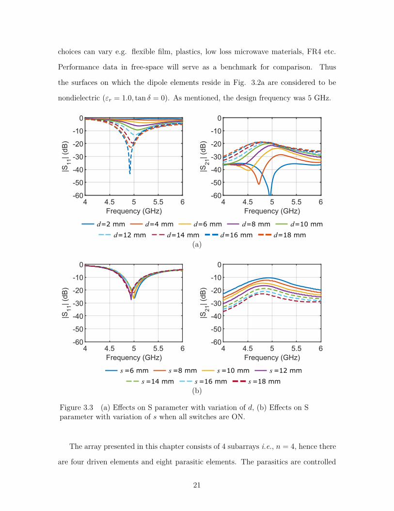
choices can vary e.g. flexible film, plastics, low loss microwave materials, FR4 etc.
Performance data in free-space will serve as a benchmark for comparison. Thus
the surfaces on which the dipole elements reside in Fig. 3.2a are considered to be
nondielectric (εr = 1.0, tan δ = 0). As mentioned, the design frequency was 5 GHz.
Frequency (GHz)4 4.5 5 5.5 6
|S1
1| (
dB)
-60
-50
-40
-30
-20
-10
0
Frequency (GHz)4 4.5 5 5.5 6
|S2
1| (
dB)
-60
-50
-40
-30
-20
-10
0
d=2 mm d=4 mm d=6 mm d=8 mm d=10 mm
d=12 mm d=14 mm d=16 mm d=18 mm(a)
Frequency (GHz)4 4.5 5 5.5 6
|S1
1| (
dB)
-60
-50
-40
-30
-20
-10
0
Frequency (GHz)4 4.5 5 5.5 6
|S2
1| (
dB)
-60
-50
-40
-30
-20
-10
0
s=6 mm s=8 mm s=10 mm s=12 mm
s=14 mm s=16 mm s=18 mm(b)
Figure 3.3 (a) Effects on S parameter with variation of d, (b) Effects on Sparameter with variation of s when all switches are ON.
The array presented in this chapter consists of 4 subarrays i.e., n = 4, hence there
are four driven elements and eight parasitic elements. The parasitics are controlled
21

using discrete RF switches. The choice of n = 4 was governed by a device that is about
150 mm long. The length and width of each planar dipole element were 25.4 mm and
2 mm, respectively. The parameter W was selected to be 10 mm considering it to
be representative of the thickness of a typical handheld device. Also, we will select
the distance, d such that the parasitic elements function as reflectors. Simulations
were performed using Ansys HFSS to optimize the array design. To represent the ON
state, each switch was modeled using a 5 pF capacitor that represented the equivalent
dc blocking capacitance for the switch. To represent the OFF state each switch was
modeled using a 0.1 pF capacitor that represented the 8 dB isolation for the switch
at this frequency.
Preliminary simulations were performed to select the parameters, d and s such
that they allow the parasitics to work as reflectors, provide good impedance matching,
and low mutual coupling. For these simulations all switches on the parasitics were
modeled as ON. First s was kept constant at 14 mm (3λ/4 center to center distance
between two consecutive sub-arrays) and d was varied. A set of simulations were
performed varying d from 2 to 18 mm. These simulation results showed that for
d < 2 mm, the parasitic elements worked as directors. Since we wanted the parasitic
elements to work as reflectors it was concluded that d > 2 mm. Important things
to consider after this was the |S11| response of each array and the mutual coupling
between to consecutive arrays as function of d. Therefore, |S11| for sub-array 1 and
the coupling between sub-arrays 1 and 2 were studied as functions of frequency, given
that the coupling between two consecutive sub-arrays is the highest. The results
presented in Fig. 3.3a show that for d ≥ 12 mm, |S11| < −10 dB and |S21| < −18
dB. In order to obtain even better |S21| performance d = 14 mm was selected.
22

4 4.5 5 5.5 6−60
−50
−40
−30
−20
−10
0
Frequency (GHz)
S11(dB)
4 4.5 5 5.5 6−60
−50
−40
−30
−20
−10
0
Frequency (GHz)
S12(dB)
4 4.5 5 5.5 6−60
−50
−40
−30
−20
−10
0
Frequency (GHz)
S13(dB)
4 4.5 5 5.5 6−60
−50
−40
−30
−20
−10
0
Frequency (GHz)
S22(dB)
4 4.5 5 5.5 6−60
−50
−40
−30
−20
−10
0
Frequency (GHz)
S24(dB)
4 4.5 5 5.5 6−60
−50
−40
−30
−20
−10
0
Frequency (GHz)
S44(dB)
Left switches ON Right switches ONAll switches ON
Figure 3.4 Simulated S parameters vs. frequency for array in free-space
Next, while d was fixed at 14 mm s was varied from 6 to 18 mm. As can be seen
from Fig. 3.3b, |S11| does not vary much with s, but |S21| does. For the initially
assumed value of s (14 mm), the |S21| is around -20 dB at 5 GHz, so this value was
kept unchanged.
23

3.3.2 Computed S Parameters for Array in Free Space
The array with d = 14 mm and s = 14 mm was then analyzed for three switch-
ing cases: Left switches ON, Right switches ON and All switches ON. The simu-
lated S parameters as functions of frequency are shown in Fig. 3.4 The array shows
overall satisfactory S parameters: |Snn|(n = 1, 2, 3, 4) < −15 dB and |Smn|(m,n =
1, 2, 3, 4, and m 6= n) < −15 dB.
2
4
6
8
10
12
90
60
300
330
300
270
240
210180
150
120
2
4
6
8
10
12
90
60
300
−30
−60
−90
−120
−150180
150
120
(a) (b)
Left switches ON Right switches ONAll switches ON
Figure 3.5 Computed realized gain patterns in free-space in the (a)h-plane (xy) and (b) e-plane (xz).
3.3.3 Simulated Radiation Patterns for Array in Free Space
Simulated array realized gain patterns at 5 GHz in the h-plane (xy) and the e-plane
(xz) are shown in Figs. 3.5a and 3.5b, respectively. As seen from Fig. 3.5a the
pattern has its peak at 0 when All switches are ON, at 30 when the Left switches
are ON and at 330 when the Right switches are ON. The e-plane pattern shows a
narrow beam (18 half-power beamwidth) as expected. The half-power beamwidth
in the h-plane is 120. The peak gain ranges from 10.7 to 11.7 dBi.
24

4 4.5 5 −60
−50
−40
−30
−20
−10
0
Frequency (GHz)
S11
(dB
)
4 4.5 5 5.5 6−60
−50
−40
−30
−20
−10
0
Frequency (GHz)
S12(dB)
4 4.5 5 5.5 6−60
−50
−40
−30
−20
−10
0
Frequency (GHz)
S13(dB)
4 4.5 5 5.5 6−60
−50
−40
−30
−20
−10
0
Frequency (GHz)
S22(dB)
4 4.5 5 5.5 6−60
−50
−40
−30
−20
−10
0
Frequency (GHz)
S24(dB)
4 4.5 5 5.5 6−60
−50
−40
−30
−20
−10
0
Frequency (GHz)
S44(dB)
Left switches ON Right switches ONAll switches ON
Figure 3.6 Simulated S parameters vs. frequency for array on FR4.
3.3.4 Array on FR4
In order to be able to experimentally fabricate and test an array the free-space de-
sign was slightly modified. For the driven and parasitic dipoles on the various faces
(Fig. 3.2a) three separate 0.8 mm thick FR4 substrates (εr = 4.5, tan δ = 0.02)
25

were considered. Dipole lengths were reduced from 25.4 mm to 20.2 mm in order
to not change the operating frequency significantly. All other parameters were un-
changed. The parameters for the array on FR4 are listed in Table 3.1. The simulated
S parameters for this array as functions of frequency are shown in Fig. 3.6. It is
apparent that the array operates at 5 GHz with |Snn|(n = 1, 2, 3, 4) < −15 dB and
|Smn|(m,n = 1, 2, 3, 4, and m 6= n) < −15 dB.
Table 3.1 Geometry parameters for array on FR4
Parameter ld lw L W d sValue (mm) 20.2 2 122.8 10 14 14
2
4
6
8
10
12
90
60
300
330
300
270
240
210180
150
120
2
4
6
8
10
12
90
60
300
−30
−60
−90
−120
−150180
150
120
(a) (b)
Left switches ON Right switches ONAll switches ON
Figure 3.7 Computed realized gain patterns on FR4 in the (a)h-plane (xy) and (b) e-plane (xz).
Simulated realized gain patterns for this array are shown in Figs. 3.7a and 3.7b.
Fig. 3.7a shows the h-plane (xy) and Fig. 3.7b shows the e-plane (xz) realized gain
patterns of the array at 5 GHz. As seen in Fig. 3.7a, the pattern has its peak at
φ = 0 when All switches are ON, at φ = 70 when the Left switches are ON and at
φ = 290 when the Right switches are ON. The half power beamwidth in the e-plane
is 20. The half-power beamwidth in the h-plane is 120. The peak gain ranges from
26

9.7 to 11 dBi. The degradation in gain (about 0.7 to 1 dB) is due to the tan δ of the
FR4 material.
(a) (b)
Figure 3.8 Configuration of the array with (a) a ground planeand (b) a ground plane and a dielectric housing (not drawn toscale).
The effect of the presence of a ground plane on antenna performance was studied.
A copper ground plane (150 × 40 mm2) was created on the same plane as one of
the parasitic antenna planes (Fig. 3.8a). It was placed at a distance, dg from the
corresponding parasitic elements. Two cases were considered, namely, dg = 5 mm and
dg = 10 mm. For both cases it was found that the effect of adding a ground plane on
S parameters was insignificant. On the other hand, a tilt in the radiation patterns
was visible. When the ground plane was placed next to the right parasitic elements,
the peak beam directions were at φ = 75, φ = 355, and φ = 240 respectively for
Left switches ON, All switches ON, and Right switches ON cases. The gain reduced
by 1 dB.
The effect of a generic dielectric housing and the ground plane on the antenna
was also studied. We considered a 150 × 70 × 10 mm3 dielectric housing ( εr = 4.4
and tan δ = .02 ) (Fig. 3.8b). The thickness of the dielectric material for the housing
was 0.8 mm and dg was 10 mm. It was found that the presence of the housing
27

caused 5% lowering of the antenna center frequency. Nevertheless, the array remained
operational at 5 GHz. The radiation patterns and gain were nearly identical to those
obtained for the array with a ground plane.
Since the array would most likely be manufactured for placement at the edge of
a mobile device other thin, low dielectric constant, low loss materials can be used,
such as plastic for example. It is unlikely that the antenna array will be made from
FR4 because the device housing will not be made from FR4. Nevertheless, we think
it is safe to assume that such material will be thin, have low dielectric constant and
lower loss compared to FR4.
3.4 Experimental Results
A laboratory prototype of the array was fabricated and measured (photographs shown
in Fig. 3.9). Each face of the array shown in Fig. 3.2a was photo-etched on a separate
0.8 mm thick FR4 substrate. The dimension of each substrate was 145×9×0.8 mm3.
Each driven dipole was fed using a 2.2 mm diameter semi-rigid 50 Ω coaxial cable and
a split coax balun made from the same cable (Fig. 3.9). Each parasitic element was
controlled using a PIN diode (Skyworks Inc. SMP1345) switch. The switch biasing
circuit shown in Fig. 3.9c contains current limiting resistor, R = 470 Ω, inductors,
L = 10 nH and capacitors, C = 10 pF. To turn the switches ON 5V dc supply was
applied. The application of 5V dc results in 9 mA of forward current allowing the
diode ON state resistance to be 1.5 Ω. And thus the expected insertion loss is 0.4
dB.
3.4.1 S-Parameter Measurements and Results
S parameter measurements were performed for the prototype shown in Fig. 3.9a.
Since a 2-port Vector Network Analyzer (VNA) was used at each time when the S-
28

parameters of two ports were measured the other two ports were terminated using 50
Ω loads. The measured S parameter data for the array are shown in Fig. 3.10.
Array Driven Parasitic Controlelement element circuit
(a)
(b) (c)
Figure 3.9 (a) Photo of the built antenna prototype (a) The arraycomponents and control circuit, (b) side-view and (c) top view of thesetup in anechoic chamber.
The measured results show that the array operates in the frequency range of 4.4
to 5.1 GHz (As |S11| ≤ −10 dB and |S21| ≤ −18 dB). Comparing the measured results
of 3.10 to the simulated results of Fig. 3.6 it can be seen that the operating frequency
for the measured is slightly lower than the simulated. The decrease in frequency is
probably due to a combined effect of imperfections in the fabrication process, non-
29

ideality of FR4 material, and the adverse effect of long bias wires which were used to
supply dc voltage to the switch control circuit.
4 4.5 5 5.5 6−60
−50
−40
−30
−20
−10
0
Frequency (GHz)
S11 (
dB
)
4 4.5 5 5.5 6−60
−50
−40
−30
−20
−10
0
Frequency (GHz)
S12 (
dB
)
4 4.5 5 5.5 6−60
−50
−40
−30
−20
−10
0
Frequency (GHz)
S13 (
dB
)
4 4.5 5 5.5 6−60
−50
−40
−30
−20
−10
0
Frequency (GHz)
S22 (
dB
)
4 4.5 5 5.5 6−60
−50
−40
−30
−20
−10
0
Frequency (GHz)
S24 (
dB
)
4 4.5 5 5.5 6−60
−50
−40
−30
−20
−10
0
Frequency (GHz)
S44 (
dB
)
Left switches ON Right switches ONAll switches ON
Figure 3.10 Selected measured S parameters vs. frequency for arrayon FR4.
3.4.2 Gain and Pattern Measurement Results
The array gain and radiation patterns were measured in a SATIMO anechoic chamber.
The setup is shown in Fig. 3.9b. As shown in Figs. 3.9a and 3.9b each driven dipole
30

is first connected to a split-coax balun and a coaxial cable. The balun resides between
two pieces of foam, each 5 mm thick. This coaxial cable then connects to another 152.4
mm long coaxial cable via a female-female SMA adapter. This cable assembly along
with three similar assemblies from the other three driven dipoles are then connected
to the 4 output ports of a 4-to-1 combiner (Minicircuits ZN4PD-642W-S+). The
input of the combiner is connected to the measurement cable of the chamber.
A microcontroller (Arduino Duemilanova) fed by a 9V battery was used to control
the bias states of all eight switches. Sixteen pieces of 381 mm long dc bias wires
were connected from the parasitic elements to the microcontroller circuit board. The
assembly is shown in Fig. 3.9c.
The cables, connectors, adapters and the combiner were measured to quantify the
combined insertion loss for the pattern and gain measurement setup that preceded
the array elements. The insertion loss was between 1.1-1.3 dB. The insertion loss was
added to the measured gain data from the anechoic chamber.
Measured realized gain patterns at several frequencies within the operating fre-
quency band are shown in Fig. 3.11. Array pattern reconfiguration in the h-plane
is apparent from Figs. 3.11a-3.11e. For all three cases, namely All switches ON,
Left switches On, and Right switches ON measured peak gain is between 8-10 dBi.
Measured antenna efficiency is about 80 %. The individual patterns for the three
cases provide a near hemispherical coverage with an average array gain of 8 dBi.
The Half-Power Beam Width (HPBW) for the All ON case is wider than the HPBW
for the other cases. Average HPBW is about 100. The E-plane patterns for one
frequency shown in Fig. 3.11f show that the beams are narrower as expected with
the HPBW of about 25. Comparing the measured patterns of Fig. 3.11 with the
simulated patterns shown in Fig. 3.7 there are signs of reflections and distortions
in the measured patterns. These are more pronounced for the case called the Right
switches ON. Ideally the h-plane patterns should be directed at 0, 70, and 290 for
31

the All ON, Left ON, and Right ON cases, respectively.
2
4
6
8
10
12
90
60
300
330
300
270
240
210180
150
120
2
4
6
8
10
12
90
60
300
330
300
270
240
210180
150
120
(a) (b)
2
4
6
8
10
12
90
60
300
330
300
270
240
210180
150
120
2
4
6
8
10
12
90
60
300
330
300
270
240
210180
150
120
(c) (d)
2
4
6
8
10
12
90
60
300
330
300
270
240
210180
150
120
2
4
6
8
10
12
90
60
300
−30
−60
−90
−120
−150180
150
120
(e) (f)Left switches ON Right switches ONAll switches ON
Figure 3.11 Measured realized gain patterns in the h-plane at (a)4.8 GHz, (b) 4.9 GHz, (c) 5 GHz, (d) 5.1 GHz, (e) 5.2 GHz, and(f) measured realized gain patterns in the e-plane at 5 GHz.
32

The differences between the simulated and measured patterns can be attributed
to the presence of the four coaxial cables and split coax baluns, the 16 dc bias wires,
and also possibly the power combiner that were not present in the simulation models.
It is expected that if lumped element chip baluns and dc bias traces made from high
resistance (>500 Ω/square) lines [104] are implemented much of the reflections and
distortions in the pattern will disappear. The simulation models did not include the
cables and the wires which are likely the cause for the discrepancies.
The performance of the proposed array is compared with some available designs
as shown in Table 3.2.
Table 3.2 Comparison of proposed array with available designs
Publication Elementno.
Meas.gain(dBi)
Freq. ofoperation(GHz)
Size (mm3) Scanangles(degree)
Qin et al. [91] 2 6 5.2 30× 30× 30.2 Not well-defined
Kishor andHum [90]
4 2.5 2.3 90× 30× 5 30, -30
Rhee et al. [92] 4 5.4 5.2 120× 40× 6 30, -30Proposed array 4 10 5 123× 10× 14 70, 0, 290
3.5 System Level Performance Analysis
3.5.1 Envelope Correlation Coefficient
Envelope Correlation Coefficient (ECC) is a metric often used for MIMO antennas
that measures the correlation between two antennas. For MIMO applications with N
antennas, the ECC between the i-th and the j-th elements is given by [105]
ρe(i, j, N) =
∣∣∣∑Nn=1 S
∗i,nSn,j
∣∣∣2∏k=i,j(1−
∑Nn=1 S
∗k,nSn,k)
. (3.3)
33

Fig. 3.12 shows the ECC for the array that was computed using the measured
S-parameter data presented in Fig. 3.10. As seen, ECC<0.01 which is excellent
for a MIMO array. This should be stated that for accurate ECC calculation far field
patterns should be used instead of S parameters as the latter method assumes lossless
antennas [106]. However for efficient antennas it can provide good approximation for
ECC [107].
4 4.5 5 5.5 6 0
0.01
0.02
0.03
0.04
0.05
Frequency (GHz)
EC
C
ρe(1,2,4)
ρe(1,3,4)
ρe(1,4,4)
ρe(2,3,4)
ρe(2,4,4)
ρe(3,4,4)
Figure 3.12 Envelope correlation coefficient frommeasured data.
3.5.2 Signal-to-Interference-plus-Noise Ratio (SINR) Performance
Finally, a system level analysis is performed to understand the performance char-
acteristics of the proposed array compared to two other antennas: a 5 dBi gain
omni-directional antenna and a MIMO array proposed by Kishor and Hum which
has two states [90]. Resource allocation study is carried out among the secondary
users (SUs) within the game theoretical framework in the heterogeneous networks
which consist of 16 primary users (PUs), 20 secondary base stations with 2 SUs in
each under one primary network (Fig. 3.13).
34

Figure 3.13 Heterogeneous Network structure with PUs, SUs, SecondaryBase Stations (SBS) within a primary cell with a Primary Base Station(PBS).
We consider that the number of available resources is 256 under the orthogonal
frequency division multiple accessing scheme, and it is assumed that all resources are
allocated by PUs. Likewise, the SUs in each secondary network are considered to use
all resources. Since the aim is to decrease the interference induced on the PUs, only
SUs are assumed to use the array by Kishor and Hum or the proposed array, i.e., PUs
are equipped with only omni-directional antenna. SINR of a SU u can be expressed
as follows,
SINRu =∑f∈F
pugufβuf∑v∈U,v 6=u pvgvfβvf +∑
b∈β pbgbfβbf + ω0(3.4)
where f = 1, 2, . . . , F is the subcarrier index, U and B show the total number of SUs
and PUs, respectively, v is the interfering SU index, u, v ∈ U , b is the PU index, pu
denotes the transmit power for user u and parameter βuf is the indicator function for
the fth subcarrier. If SU u uses the fth subcarrier,βuf = 1, otherwiseβuf = 0. ω0is
the additive white Gaussian noise.
35

Figure 3.14 Comparison of the proposed array withomni-directional antenna and array by Kishor andHum.
Fig. 3.14 shows the performance results of the proposed array, omni-directional
antenna and PIFA in terms of SINR. As seen from the figure, proposed array out-
performs the standard antennas. While 50% of the SINR values are only below 19
dB and 20 dB respectively for the omni-directional antenna and the Kishor and Hum
antenna, respectively 50% of the SINR values are below 33 dB for our proposed ar-
ray. In other words, the gain in mean SINR of the Kishor and Hum antenna over the
omnidirectional antenna is 2.5%. The same for the proposed antenna over an om-
nidirectional antenna is 59%. This indicates that the SUs can achieve higher SINR
values with proposed array. This result can also be confirmed from Fig. 3.15 which
shows the mean SINR gain obtained in each SU. As shown in Fig. 3.15, almost every
SU achieves higher gain with proposed array. System level results indicate that the
proposed array is a strong candidate for the user devices in heterogeneous networks.
This result can also be proved in Fig. 3.15 which shows the mean SINR gain ob-
tained in each SU. As shown in Fig. 3.15, almost every SU achieves higher gain with
36

proposed array. System level results indicate that the proposed array is a strong
candidate for the user devices in heterogeneous networks.
0 5 10 15 20 25 30 35 400
10
20
30
40
50
60
70
80
User Index
SIN
R (
dB)
Omni-directional Array by Kishor&Hum Proposed array
Figure 3.15 Mean SINR gain of each SU.
37

Chapter 4
High Gain Beam Steering Arrays for Wearable
Wireless Applications
4.1 Introduction
Body-centric wireless communication is a rapidly growing field which can be classified
into three types: Off-body, on-body, and in-body communication [108]. If only one
antenna in the communication link remains on body and rest of the link is outside
the body (in the surrounding place) it is called off-body communication. This sets
up the communication between local base stations and the antenna on body, which
can be a wearable or textile antenna. If all antennas are on the surface of the body
and hence the communication link is also on the surface of the body it is called the
on-body domain. And if most of the antennas or sensors are implanted inside the
body it is referred to be the in-body domain. This includes the implantable chips
and sensors. In this chapter we will focus on off-body communications.
Many fixed beam antennas have been proposed for off-body communication which
suffer from gain degradation in multipath rich environment causing low data rate and
low reliability[108]. It has been shown that pattern reconfigurable MIMO arrays can
perform better in these situations [22]. As mentioned earlier, pattern reconfiguration
can be achieved using phased arrays but that will make the array too large and costly
to implement for wearable communications. Parasitic arrays are a good alternative
for low cost smaller footprint applications.
Recently, in our group, we introduced the concept of high-gain compressed foot-
38

print switched parasitic beam steering array for 0.9 GHz, 2.45 GHz and 5 GHz wear-
able application [101–103]. The 0.9 GHz and 2.45 GHz array each consists of a single
subarray with one driven element and thus has low gain. The 5 GHz array is a high
gain collinear array consisting of multiple driven and parasitic elements but it uses a
thick foam substrate which is impractical for wearable applications.
In this chapter we present the design of a thin high-gain beam steering collinear
antenna array based on realistic fabric materials which can be integrated within the
clothing or uniform of a person. The robustness of the design is demonstrated with
material sensitivity analysis and performance studies on a curved surface and near a
multilayered body phantom. Loss tangent measurement data for fabric substrate is
presented.
4.2 Materials for the Proposed Wearable Antenna
Properly selecting non-conductive fabric substrates is important while designing and
developing wearable antenna arrays. RF properties that are highly desired are low
dielectric constant, εr and low loss tangent, tan δ. Low dielectric constant allows wider
bandwidth while low tan δ allows high gain. Mechanical/structural properties that
are greatly desired are flexibility/malleability, homogeneity, and very low tendency
to absorb moisture.
Table 4.1 Dielectric properties of variousnon-conductive fabric materials.
Nonconductive Fabric εr tan δCordura 1.90 0.0098Cotton 1.60 0.0400100 % polyester 1.90 0.0045Quartzel fabric 1.95 0.0004Lycra 1.50 0.0093
In general, the dielectric properties of a textile material depend on the frequency,
39

temperature, surface roughness, moisture content, purity and homogeneity of the
material [109]. The fabric materials are generally anisotropic because of the weaving
pattern of the fibers or yarns. Non-conductive fabrics are also porous materials with
εr varying from 1.2 to 2. The εr and tan δ of various fabrics are shown in Table 4.1
[110].
Moisture content in fabric materials is a key contributor in εr change. Typically
the higher the moisture content the higher is the εr. The sensitivity of fabrics to
moisture is characterized using the term ‘regain’ [109], which is defined as
Regain = Mass of water absorbedMass of dry specimen × 100%. (4.1)
Regain is related to relative humidity (RH). It is reported that at 65% RH, wool
fiber, cotton and polyester might present a regain of 14.5%, 7.5% and 0.2% respec-
tively, which shows that Polyester is much less sensitive to humidity [109].
Similarly to fabricate antennas that can be formed or shaped to go with body
contour conductive fabrics can be used. Various conductive fabrics Flectron [111],
ShieldIt, Copper taffeta, Nickel Copper Ripstop, Ripstop Silver [112] etc. have been
reported in the literature. Key properties include electric surface resistivity, ρs which
is related to conductivity, σ, and fabric thickness, t
σ = 1ρst
. (4.2)
Table 4.2 shows the ρs, t, and σ of some commonly used conductive fabrics.
Table 4.2 Electrical properties of various conductive fabrics.
Conductive Fabric Surface re-sistivity, ρs(Ω/Sq.)
Thickness,t (mm)
Conductivity,σ (S/m)
Flectron 0.07 0.2 7.14× 10⁴
ShieldIt 0.50 0.15 1.33× 10⁴
Copper Taffeta 0.05 0.08 6.67× 10⁵
Nickel Copper Ripstop 0.03 0.08 4.16× 10⁵
Ripstop Silver 0.25 0.05 8× 10⁴
40
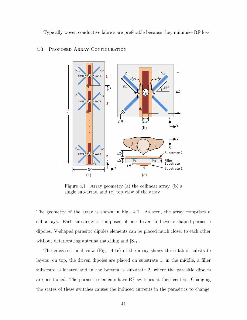
Typically woven conductive fabrics are preferable because they minimize RF loss.
4.3 Proposed Array Configuration
Figure 4.1 Array geometry (a) the collinear array, (b) asingle sub-array, and (c) top view of the array.
The geometry of the array is shown in Fig. 4.1. As seen, the array comprises n
sub-arrays. Each sub-array is composed of one driven and two v-shaped parasitic
dipoles. V-shaped parasitic dipoles elements can be placed much closer to each other
without deteriorating antenna matching and |S11|.
The cross-sectional view (Fig. 4.1c) of the array shows three fabric substrate
layers: on top, the driven dipoles are placed on substrate 1, in the middle, a filler
substrate is located and in the bottom is substrate 2, where the parasitic dipoles
are positioned. The parasitic elements have RF switches at their centers. Changing
the states of these switches causes the induced currents in the parasitics to change.
41

Three switching states are considered: only the left switches are ON, only the right
switches are ON, and all switches are ON. This allows the array beam to steer in
three different directions in the azimuth (xy) plane. The parameters that were kept
constant throughout the study were: dL = 22.6 mm, dW = 3 mm, pL = 10.8 mm,
pw = 1 mm, and t = 2 mm. All fabric substrates were assumed to have a relative
permittivity, εr of 1.7 and loss tangent of 0.001.
4.4 Simulation Results
4.4.1 Array Design and Optimization
(a) (b)
Figure 4.2 (a) Simulated |S11| vs. frequency for differentvalues of dx and dy, and (b) simulated |S21| vs. frequency fordifferent values of s.
The design and optimization of the array were performed using Ansys HFSS. The
ON state of the switch was modelled using a SHORT while the OFF state was mod-
elled using a 0.01 pF capacitor. First, the values of the parameters dx and dy were
determined in order to discern whether the parasitic elements would act as reflectors
or directors [103]. Parametric simulations were performed showing that dx could be
as small as 1 mm (Fig. 4.2a), thus allowing the total thickness to be 5 mm. The
parameter dy was kept fixed at 4 mm. The parameter, s determines the mutual
coupling between two consecutive collinear elements. When s was varied from 16 to
24 mm, |S21| improved from -17 to -24 dB with all switches being ON (Fig. 4.2b).
42
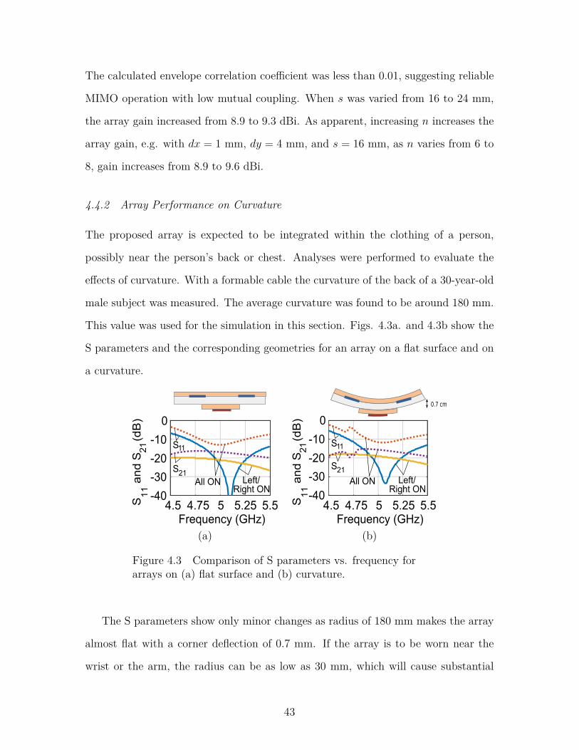
The calculated envelope correlation coefficient was less than 0.01, suggesting reliable
MIMO operation with low mutual coupling. When s was varied from 16 to 24 mm,
the array gain increased from 8.9 to 9.3 dBi. As apparent, increasing n increases the
array gain, e.g. with dx = 1 mm, dy = 4 mm, and s = 16 mm, as n varies from 6 to
8, gain increases from 8.9 to 9.6 dBi.
4.4.2 Array Performance on Curvature
The proposed array is expected to be integrated within the clothing of a person,
possibly near the person’s back or chest. Analyses were performed to evaluate the
effects of curvature. With a formable cable the curvature of the back of a 30-year-old
male subject was measured. The average curvature was found to be around 180 mm.
This value was used for the simulation in this section. Figs. 4.3a. and 4.3b show the
S parameters and the corresponding geometries for an array on a flat surface and on
a curvature.
0.7 cm
(a) (b)
Figure 4.3 Comparison of S parameters vs. frequency forarrays on (a) flat surface and (b) curvature.
The S parameters show only minor changes as radius of 180 mm makes the array
almost flat with a corner deflection of 0.7 mm. If the array is to be worn near the
wrist or the arm, the radius can be as low as 30 mm, which will cause substantial
43
deflection, frequency shift or gain degradation is possible for that case. The array on
the curved surface resulted in a small increase in the gain (gain increased from 8.9 to
9.1 dBi when all switches were ON).
4.4.3 Material Sensitivity
Simulation results of the array considering four different types of fabrics show that
the array performs well. The dielectric properties of these materials were obtained
from [113]. For all cases, |S11| < −10 dB and |S21| < −15 dB were found. The gain
at 5 GHz for all cases are listed in Table 4.3.
Table 4.3 Gain variation with different types of fabrics.
Fabric type Polyester(εr = 1.5)
Polycot(εr = 1.6)
Jeans cot-ton (εr =1.7)
Fine wo-ven cotton(εr = 2.0)
Peak Gain (dBi) [AllSwitches ON]
9.7 9.3 9 7.9
Peak Gain (dBi)[Only Left/RightSwitches ON]
10.5 10.6 10.9 10.7
4.4.4 Array Performance near Human Body
The array was analyzed near a multilayered flat human phantom composed of 2 mm
thick skin, 5 mm thick muscle and 10 mm thick bone layers (Fig. 4.4a). A spacer
fabric is placed between the array and human body. The tissue properties at 5
GHz were obtained from IT’IS Foundation based in Zurich, Switzerland. The tissue
properties at 5 GHz are listed in Table 4.4.
Table 4.4 Human tissue properties at 5 GHz.
Tissue εr σ(Sm−1)Skin (2 mm) 35.80 3.06Muscle (5 mm) 49.50 4.04Bone (10 mm) 10.00 0.962
44

At a distance of 5 mm from the phantom, the array beam points to 30, 0, and
330 for left switches ON, all switches ON and right switches ON, respectively (Fig.
4.4b). At 10 mm, the array beam points to 45, 0, and 315 (Fig. 4.4c) with gain
varying between 11.7 to 12.3 dBi. The half-power beamwidth in the azimuth plane
was 90. In the elevation plane the beamwidth is 20 (Fig. 4.4d).
h
SkinMuscleBone
Antenna
Spacerfabric
h= 5 mm(a) (b)
h= 10 mm h= 10 mm(c) (d)
Figure 4.4 (a) Top view of the array nearmultilayered body phantom, realized gain patterns forthis set up in the (b) azimuth (XY) plane when h = 5mm, (c) azimuth (XY) plane when h = 10 mm, and (d)elevation (ZX) plane when h = 10 mm.
4.5 Experimental Results
A microstrip patch antenna was built using a 2.7 mm thick cotton material (90%
cotton, 10% olefin) as substrate and it was then compared with simulation results
45
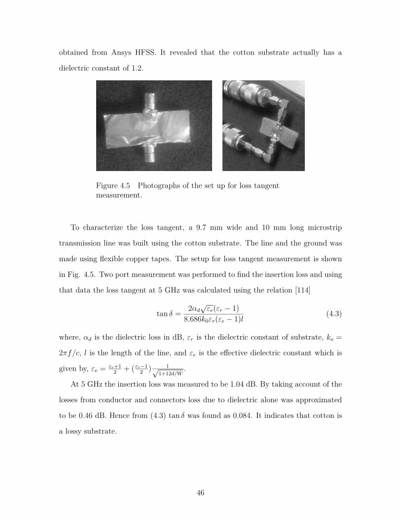
obtained from Ansys HFSS. It revealed that the cotton substrate actually has a
dielectric constant of 1.2.
Figure 4.5 Photographs of the set up for loss tangentmeasurement.
To characterize the loss tangent, a 9.7 mm wide and 10 mm long microstrip
transmission line was built using the cotton substrate. The line and the ground was
made using flexible copper tapes. The setup for loss tangent measurement is shown
in Fig. 4.5. Two port measurement was performed to find the insertion loss and using
that data the loss tangent at 5 GHz was calculated using the relation [114]
tan δ = 2αd√εe(εr − 1)
8.686k0εr(εe − 1)l (4.3)
where, αd is the dielectric loss in dB, εr is the dielectric constant of substrate, ko =
2πf/c, l is the length of the line, and εe is the effective dielectric constant which is
given by, εe = εr+12 + ( εr−1
2 ) 1√1+12d/W
.
At 5 GHz the insertion loss was measured to be 1.04 dB. By taking account of the
losses from conductor and connectors loss due to dielectric alone was approximated
to be 0.46 dB. Hence from (4.3) tan δ was found as 0.084. It indicates that cotton is
a lossy substrate.
46
Chapter 5
Thin Switched Beam Parasitic Array on a
Non-Uniform Aperiodic (NUA) Metasurface
5.1 Introduction
Increasing interest in wearable technologies is creating demands for high performance
broadband antennas. Dipole type antennas are considered as good choices for broad-
band operation. But they need to be properly isolated from the human body in order
to reduce losses. Isolation can be achieved by placing a ground plane between the
antenna and the body. But if the ground plane is too close to the antenna the return
loss and gain degrade. This problem can be solved with the help of a well-designed
Electromagnetic Band Gap (EBG) structure.
EBG materials are engineered materials which suppress electromagnetic wave in
any given spatial direction within a certain frequency range. They have also been
called High Impedance Surfaces (HIS), Artifial Magnetic Conductor (AMC), and
Artifial Impedance Surfaces (AIS). Electromagnetic bandgap (EBG) materials are
also known as photonic bandgap (PBG) materials or photonic crystals (PC). In 1987
Yablonovitch proposed that it should be possible to create three dimensional periodic
structures that would exhibit electromagnetic band gap properties [115]. The idea
was later expanded by John [116]. The existence of such band gap was experimentally
established by Ho et al. [117]. Later Yablonovitch et al. experimentally showed that
the Face Centered Cubic (FCC) structure could also be used as a PBG structure if
holes were drilled into that structure [118]. In 1994 the ‘wood-pile’ structure was
47

proposed [119] and materialized [120]. Meanwhile soft and hard surfaces were pro-
posed in [121]. In 1999 Sievenpiper et al. proposed the mushroom-like EBG as a high
impedance surface (HIS) which inhibited the propagation of surface waves within a
certain frequency band [122, 123]. Yang et al. developed uniplanar compact EBGs
(UC-EBG) which showed a behavior similar to the mushroom-like EBG [124, 125].
Generally most of the EBG structures that have been proposed have periodic geom-
etry. With the discovery of quasi crystals in solid-state physics aperiodic EBGs have
also been introduced [126]. Other examples of EBGs and their analysis methods can
be found in [127–132].
Research on antennas integrated with EBG materials dates back at least ten years
[122, 123]. Since then there have been many research publications on the subject mat-
ter some on high performance microstrip patch antenna design [132–139], some on
slot and circularly polarized antenna design [140–145] and some on directional dipole
antenna design [146–156] using EBGs. Many commercial and military applications
need directional dipole antennas that can be flush mounted on the surface of a ve-
hicle, such as an aircraft. Yet the presence of the ground plane below the dipole
poses a challenging environment to develop very thin conformal antennas especially
in the lower GHz frequency range. Typically if no additional dielectric or magnetic
loading is used the antenna height can very well exceed 3-5 inches at UHF (Ultra
High Frequency) frequencies which is highly undesirable. The application of a well-
designed EBG metamaterial as a supporting structure in between the dipole and the
ground plane can alleviate this situation. Hansen’s analytical work [147] explained
the interaction between a dipole antenna and the reflection phase of an EBG struc-
ture. The authors of [148] performed FDTD simulations of the reflection phase and
a dipole antenna and obtained a certain range of phase angles that provided a better
impedance match for a dipole.
Akhoondzadeh-Asl et al. [153] introduced a wideband (bandwidth = 1.7) diamond
48

dipole on an EBG structure with a total thickness of 0.07λ0. In our research group,
Abedin et al. [152] introduced the concept of impedance modulation to develop
an ultrathin printed dipole antenna (height = 0.025λ0) .The impedance of a driven
dipole antenna was modulated by the reflection phase of an EBG structure [152].
Also, in our research group, Azad et al. [155] introduced the design methodology
of a wideband (bandwidth = 1.4) dipole on EBG where the interplay between the
EBG reflection phase and the impedance of the dipole antenna were exploited to
design a thin (0.03λ0) directional dipole. The experimental prototype of a wideband
(bandwidth = 1.5) bowtie dipole on EBG reported by Best et al. [156] had an
EBG height of 0.05λ0. Tunable EBG surfaces using varactor diodes have also been
introduced in [157–159]. However, they need complicated circuitry and have the
potentials of emitting higher order harmonics especially at high power because of
device non-linearity. Other broadband EBG structures that have been proposed
include a periodic structure with unit cells consisting of different sizes of patches
cascaded [160].
The summary of research activities on EBGs clearly delineate that it has been a
difficult journey to reconcile the two contradictory requirements, broad bandwidth
and thin very low profile design using uniform mushroom type EBG structures. The
premise of this work was to address this subject from the point of a Non-Uniform
Aperiodic (NUA) EBG structure. Instead of following the traditional route of illumi-
nating the EBG surface using a plane wave source then computing its reflection phase
as function of frequency and then matching it with the antenna resonant frequency
we follow our previously demonstrated concept of impedance modulation [152, 155].
The latter is more logical and consequential as because the antenna is almost always
operated in the near field of the EBG surface. We consider the EBG surface to be
an impedance transformer that provides the necessary matching for the dipole. In
support of this claim consider the works reported in [117, 127, 129, 161]. We have
49
found that the total electrical dimensions of the two sides of the square mushroom
patch,w and its via height, h is (2w + h√εreff ) which is approximately a quarter
wave length at the respective center frequencies considering εreff = (εr + 1)/2. Thus
the quarter wave impedance transformer e.g. the uniform mushroom EBG surface
presents a good match for the dipole antenna within its frequency of operation.
However, since the use of uniform mushroom EBG transformer has apparently
reached its limits in terms of bandwidth potential for a specific thickness it is logical
to consider a NUA EBG surface as a better alternative. The analogy is that of
impedance matching using a standard quarter wave transformer (narrowband) versus
impedance matching using multi-section transformers (broadband) where the former
is analogous to the uniform EBG while the latter is analogous to the NUA EBG.
Hence we model and analyze the antenna and the EBG together and then examine the
impedance perturbation of the dipole as function of the EBG geometrical parameters.
The goal of this paper is to explore the prospects of designing and developing a one
octave bandwidth directional antenna on a NUA EBG surface with a total thickness
of 1 inch (0.04λ0) or less for operation starting at 450 MHz. The contemporary
term metasurface has come to encompass any parasitic loading structure consisting
of numerous small inclusions. This work represents a fully developed detailed version
of our more recent conference presentation [67].
The chapter is organized as follows: first, the design of a UHF broadband fat strip
dipole antenna on a traditional uniform mushroom EBG surface is presented. Sec-
ond, a tapering scheme is introduced to generate a NUA metasurface that maintains
the same volume as the traditional mushroom EBG surface. Using the proposed
percent tapering scheme the dimensions and spacing of the patches for the NUA
EBG surface can be generated. The geometrical tapering is achieved where the in-
dividual patches and their spacings are tapered according to a percent (prescribed)
taper profile. Third, Simulation results of various tapering profiles are presented from
50
which the optimum tapering is selected that allows broadband operation. Fourth, the
magnetic fields on the proposed NUA metasurface are compared to those on a con-
ventional mushroom EBG and their differences are identified. Fifth, an experimental
laboratory prototype of a UHF metasurface dipole is fabricated and tested for VSWR,
pattern, and gain. Finally, based on the NUA-EBG concept design, we present the
study and design of a very thin planar pattern reconfigurable antenna on EBG for
operation in the 2.4 GHz ISM band. The EBG in conjunction with the parasitic array
approach allows beam steering at -25 (335), 0, and 25 degrees which otherwise would
have been -90 (270), 0, and 90 degrees without the EBG. The goal of investigating
and designing the beam steering array on EBG structure was geared towards reducing
its total thickness while achieving very high (F/B). A second objective was to attain
a slight tilt in the array beam from the 90 and 270 degree directions.
5.2 Fat Strip Dipole Antenna on a Uniform Mushroom Type EBG
As a starting point, a wideband fat strip dipole operating against a mushroom type
EBG structure was considered. Although a fat bow-tie dipole could have been used,
a rectangular dipole was used for simplicity. The objective was to understand the
maximum VSWR, pattern, and gain bandwidths that can be obtained under such an
approach.
5.2.1 Fat Strip Dipole Antenna in Free-Space
The fat strip dipole shown in Fig. 5.1a consisted of two conducting strips each
measuring 160 mm (length) by 110 mm (width). The two metal strips were separated
by a 10 mm gap and was excited using a lumped port in HFSS. Simulated VSWR
vs. frequency for this antenna in free-space are shown in Fig. 5.1b. As apparent, the
antenna operates from 300-900 MHz within VSWR < 3. The patterns (not shown)
resemble those of a half-wave dipole within the frequency range of 330-900 MHz (a
51

ratio of 2.7:1).
(a)
(b)
Figure 5.1 (a) Fat strip dipole; W = 110 mm,L = 160 mm and (b) its simulated VSWR.
5.2.2 UHF Wideband Dipole on Uniform Mushroom EBG Surface
Following our previous work in the 1750-2500 MHz frequency band on wideband
dipole design on mushroom type EBGs [155], the unit cell size of a baseline uniform
mushroom EBG was determined for operation at 450 MHz and above. This was
about a factor of 4 size increase compared to the EBG design in [155]. The UHF
mushroom EBG surface consists of 8 by 8 conducting patches each measuring 50 mm
by 50 mm (Fig. 5.2). Each patch is separated from the other by a distance of 5 mm.
The total length of the square EBG surface was 435 mm. Each EBG patch contained
a 2 mm diameter conducting post at its center that connected it to the conducting
ground plane below (Fig. 5.2). The total EBG thickness, h1 + h2 was 25 mm and
52

both εr1 = εr2 = 4.5 (FR4). The strip dipole described above was placed h3 = 1 mm
above the EBG.
(a)
(b) (c)
(d) (e)
Figure 5.2 (a) A fat dipole antenna on a uniform mushroom-EBG, (b)top view, (c) simulated VSWR response. (d) simulated radiation patternsat 450 MHz, and (e) simulated 3D pattern at 550 MHz.
Simulated VSWR vs. frequency results for this case are plotted in Fig. 5.2c
wherefrom it is apparent that the antenna on this EBG operates from 430 MHz to
620 MHz. The frequency ratio is 1.4 or the VSWR bandwidth is 40%. This bandwidth
53
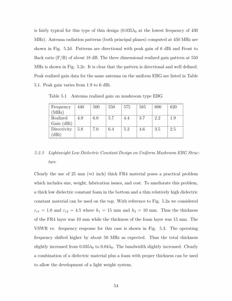
is fairly typical for this type of thin design (0.035λ0 at the lowest frequency of 430
MHz). Antenna radiation patterns (both principal planes) computed at 450 MHz are
shown in Fig. 5.2d. Patterns are directional with peak gain of 6 dBi and Front to
Back ratio (F/B) of about 18 dB. The three dimensional realized gain pattern at 550
MHz is shown in Fig. 5.2e. It is clear that the pattern is directional and well defined.
Peak realized gain data for the same antenna on the uniform EBG are listed in Table
5.1. Peak gain varies from 1.9 to 6 dBi.
Table 5.1 Antenna realized gain on mushroom type EBG
Frequency(MHz)
440 500 550 575 585 600 620
RealizedGain (dBi)
4.9 6.0 5.7 4.4 3.7 2.2 1.9
Directivity(dBi)
5.8 7.0 6.4 5.2 4.6 3.5 2.5
5.2.3 Lightweight Low Dielectric Constant Design on Uniform Mushroom EBG Struc-
ture
Clearly the use of 25 mm (≈1 inch) thick FR4 material poses a practical problem
which includes size, weight, fabrication issues, and cost. To ameliorate this problem,
a thick low dielectric constant foam in the bottom and a thin relatively high dielectric
constant material can be used on the top. With reference to Fig. 5.2a we considered
εr1 = 1.0 and εr2 = 4.5 where h1 = 15 mm and h2 = 10 mm. Thus the thickness
of the FR4 layer was 10 mm while the thickness of the foam layer was 15 mm. The
VSWR vs. frequency response for this case is shown in Fig. 5.3. The operating
frequency shifted higher by about 50 MHz as expected. Thus the total thickness
slightly increased from 0.035λ0 to 0.04λ0. The bandwidth slightly increased. Clearly
a combination of a dielectric material plus a foam with proper thickness can be used
to allow the development of a light weight system.
54
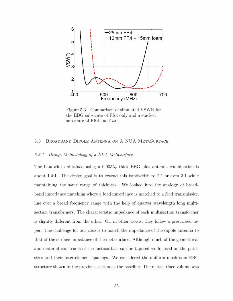
Figure 5.3 Comparison of simulated VSWR forthe EBG substrate of FR4 only and a stackedsubstrate of FR4 and foam.
5.3 Broadband Dipole Antenna on A NUA MetaSurface
5.3.1 Design Methodology of a NUA Metasurface
The bandwidth obtained using a 0.035λ0 thick EBG plus antenna combination is
about 1.4:1. The design goal is to extend this bandwidth to 2:1 or even 3:1 while
maintaining the same range of thickness. We looked into the analogy of broad-
band impedance matching where a load impedance is matched to a feed transmission
line over a broad frequency range with the help of quarter wavelength long multi-
section transformers. The characteristic impedance of each multisection transformer
is slightly different from the other. Or, in other words, they follow a prescribed ta-
per. The challenge for our case is to match the impedance of the dipole antenna to
that of the surface impedance of the metasurface. Although much of the geometrical
and material constructs of the metasurface can be tapered we focused on the patch
sizes and their inter-element spacings. We considered the uniform mushroom EBG
structure shown in the previous section as the baseline. The metasurface volume was
55

kept constant at 435 × 435 × 25 mm3 and the dielectric material was FR4 for both
εr1 and εr2 shown in Fig. 5.2a. The design scheme followed here can be described as
follows:
• A mushroom like metasurface consisting of n by n conducting patches is placed
on n/2 concentric square rings. The innermost ring (ring 1) is shown in Fig.
5.4 using a dotted outline. Thus the outermost ring is ring number n/2. The
i-th ring has 4(2i− 1) number of patches where i = 1, 2, 3, . . . , n/2
• While in a conventional mushroom EBG structure all square patches have the
same dimension in the proposed NUA metasurface the square patches in the
same i-th ring have the same dimension but in a different i-th ring they have
different dimension. Thus there is a tapering as we move from one square ring
to the other. Let any square of the i-th ring have a side length, ai.
• Also for a conventional mushroom EBG surface the spacing between two con-
secutive rings i.e., inter-ring spacing and the spacing between two consecutive
patches in a same ring i.e., intra-ring spacing is the same. In a NUA metasur-
face the intra-ring spacing or the spacing between the individual patches in the
same ring is fixed but the inter-ring spacing is tapered. Let the spacing between
two consecutive patches in the central ring be s1, the spacing between rings 1
and 2 be s2, and the spacing between rings 2 and 3 be s3 and so on.
• The tapering can be described as follows
ai+1 = rai (5.1)
si+1 = rsi (5.2)
where i = 1, 2, 3, . . . (n/2− 1) and
r = (1± p
100) (5.3)
56

where p is the percent increase or decrease in the patch size (plus sign in equa-
tion (5.3) for increase and minus sign in equation (5.3) for decrease) and the
parameters and are determined as follows.
• Let abase be the width of the square patches of the conventional mushroom EBG
surface. Then a1 is found by letting abase be the average of the different patch
widths, a1 to an/2.
a1 + a2 + · · ·+ an/2 = n
2abase (5.4a)
or, a1 + ra1 + · · ·+ r(n/2−1)a1 = n
2abase (5.4b)
or, a1 = n
2abase(r − 1)r(n/2) − 1 (5.4c)
• The variable s1 is found by keeping the total length, L constant
2(a1 + a2 + · · ·+ an/2) + (s1 + 2s2 + 2s3 + · · ·+ 2sn/2) = L (5.5a)
or, s1 = L(r − 1)− 2a1(rn/2 − 1)2(rn/2 − 1)− (r − 1) (5.5b)
For example, for n = 8, L = 435 mm, abase = 50 mm and p = 20 (for 20%
decreasing taper) the parameter values listed in Table 5.2 will be the result. The
corresponding geometry is shown in Fig. 5.4. Similarly, for a 15% increasing taper,
the dimensions listed in row 5 of Table 5.2 will be the result.
As stated earlier, for the studies and design of this paper, n = 8 was considered.
However, the dimensions for n = 10 and n = 12 with a 20% decreasing taper are
given in Table 5.3. These dimensions were arrived at by considering the same patch
size and spacing as that of the uniform mushroom-type EBG, obtaining a1 and then
L from (5.1) to (5.5).
57

Figure 5.4 Top view of a NUA metasurface with20% decreasing taper.
Table 5.2 Patch width (in mm) and inter-element spacing (in mm).
Taper profile a1 a2 a3 a4 s1 s2 s3 s42% increase 48.4 49.3 50.4 51.4 4.9 5 5.1 5.24% increase 47 48.9 50.8 52.9 4.7 4.9 5.1 5.310% increase 43.1 47.4 52.1 57.4 4.2 4.6 5.1 5.615% increase 40 46 53 60.9 3.9 4.5 5.1 5.92% decrease 51.4 50.4 49.3 48.4 5.3 5.2 5.1 54% decrease 53 50.9 48.8 46.9 5.4 5.2 2 4.810% decrease 58 52.2 47 42.3 6 5.4 4.9 4.415% decrease 63 53.5 42.5 38.7 6.2 5.3 4.5 3.820% decrease 68 54.4 43.5 34.8 6.8 5.4 4.4 3.5
Table 5.3 Patch width (in mm) and interelement spacing (in mm) for 20%decreasing taper for different number of elements.
n a1 a2 a3 a4 a5 a6 s1 s2 s3 s4 s5 s6 L8 68 54.4 43.5 34.8 6.8 5.4 4.4 3.5 43510 74.4 59.5 47.6 38 30.5 7.9 6.3 5 4 3.2 54512 81.3 65 52 41.6 33.3 26.6 8.6 6.9 5.5 4.4 3.5 2.8 655
As shown, with n = 8, the maximum to minimum patch size has a ratio of 2.
This ratio increases to 2.4 and 3, respectively, for n = 10 and n = 12. Moreover,
58

note that, with increasing n, the total dimension L increases. As we will observe
later, the parameter L has an important influence on the antenna radiation pattern,
particularly when it is one wavelength.
Choosing too few patches would make the structure too small to fully support
the near fields of the radiating element. This will also create undesirable amount
of high back radiation. The number of patches, i.e., 8 by 8, and the patch sizes
chosen for UHF band design in this paper, was a compromise in that respect. Our
premise is such that, if one wishes to use n = 10 or 12, then one should determine
the patch sizes and spacing based on the baseline design metric first and by using
the equations provided. The baseline design metric is a quarter-wave transformer as
explained earlier in Section 1. However, it should be noted that a change in n may
require finding an optimum design that entails determining the proper amount of
taper, the dipole size, and the dipole height.
5.3.2 Simulation Results of Increasing Taper
Initially, NUA structures with increasing taper was considered. For example, the
patch dimensions and spacings for 2%, 4%, 10% and 15% increase are listed in Table
5.2. The total length, mm was kept unchanged and was considered. Substrate ma-
terial and thickness was also unchanged (FR4, 25 mm thick). Each patch contained
a 2 mm diameter via as before. Numerous simulations were performed among which
the results of several simulations are shown in Figs. 5.5 and 5.6.
Observing the VSWR results shown in Fig. 5.5 it is clear that they do not show
any sign of improvement in antenna bandwidth. Actually, the bandwidth worsens as
the amount of taper increases. We should note that the operation of the dipole against
this AIS manifests itself as a coupled resonance phenomenon as seen in Fig.5.6a, where
only a slight taper (2% increasing) has been introduced. There are two visible knots
that contain the frequency ranges of 420-475 MHz and 500-600 MHz, respectively.
59
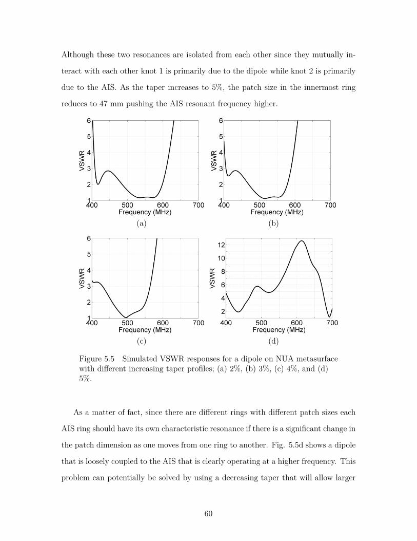
Although these two resonances are isolated from each other since they mutually in-
teract with each other knot 1 is primarily due to the dipole while knot 2 is primarily
due to the AIS. As the taper increases to 5%, the patch size in the innermost ring
reduces to 47 mm pushing the AIS resonant frequency higher.
(a) (b)
(c) (d)
Figure 5.5 Simulated VSWR responses for a dipole on NUA metasurfacewith different increasing taper profiles; (a) 2%, (b) 3%, (c) 4%, and (d)5%.
As a matter of fact, since there are different rings with different patch sizes each
AIS ring should have its own characteristic resonance if there is a significant change in
the patch dimension as one moves from one ring to another. Fig. 5.5d shows a dipole
that is loosely coupled to the AIS that is clearly operating at a higher frequency. This
problem can potentially be solved by using a decreasing taper that will allow larger
60

size patches near the dipole region and smaller size patches away from the dipole
which is the subject matter of the discussion in the following section.
(a) (b)
(c) (d)
Figure 5.6 Simulated impedance Vs. frequency data fordipole on NUA metasurface with different increasing taperprofiles; (a) 2%, (b) 3%, (c) 4%, and (d) 5%.
5.3.3 Simulation Results of Decreasing Taper
Based on the observations and the understanding from before cases of decreasing taper
were considered next. Several cases of patch dimensions and spacing with decreasing
taper are listed in Tables 5.2 and 5.3. As apparent, any amount of decreasing taper
results in larger size patches near the center and smaller size patches away from
the center. Fig. 5.7 shows the simulated VSWR vs. frequency characteristics for a
61

number of cases with decreasing tapering. Corresponding impedance vs. frequency
characteristics are shown in Fig. 5.8.
(a) (b)
(c) (d)
(e) (f)
Figure 5.7 Simulated VSWR response of dipole on NUA metasurfacewith different decreasing taper profiles; (a) 2%, (b) 4%, (c) 10%, (d) 15%,(e) 20%, and (f) 20% tapering with dipole arm length adjusted to 120 mmeach.
62

(a) (b)
(c) (d)
(e) (f)
Figure 5.8 Simulated impedance Vs. frequency for dipoleon NUA metasurface with different decreasing taper profiles:(a) 2%, (b) 4%, (c) 10%, (d) 15%, (e)20%, (f) 20% taperingwith arm length of the dipole adjusted to 120 mm each.
Comparing Figs. 5.6a and 5.8a within the 400-700 MHz frequency range one can
63

observe that there are three visible knots for the latter while two for the former. As
the amount of decreasing taper increases, increased coupling between the dipole and
the AIS surface is observed. At 20% decreasing taper (Fig. 5.8e) it is clear that
there is significant coupling and hence bandwidth potential if the top and bottom
knots on the center of the Smith chart can be moved further to the center. That
is when adjusting the dipole length was attempted. The simulation results with the
dipole length as the parameter are shown in Fig. 5.9. By gradually reducing the
dipole length the coupling between the dipole and the AIS was made to be optimum
resulting in a broadband response as seen in Fig. 5.7e.
(a) (b)
(c) (d)
Figure 5.9 Simulated impedance Vs. frequency for dipole onNUA metasurfaces with 20% decreasing taper profile. (a) armlength= 156 mm, (b) arm length= 140 mm, (c) arm length= 120mm, and (d) arm length= 100 mm.
64

5.3.4 An Effective Antenna EBG system
The results shown in Fig. 5.7e show clear potential for broad bandwidth extending
from 320-680 MHz within VSWR < 3:1 which is more than an octave. Although in
some regions across the frequency band the VSWR exceeds 3:1, it is expected that
further tuning will reduce these numbers. Simulated peak realized gain patterns are
shown in Figs. 5.10 and 5.11.
(a) (b)
(c) (d)E-Plane H-Plane
Figure 5.10 Simulated realized gain patterns at (a) 319MHz, (b) 450 MHz, (c) 550 MHz, and (d) 600 MHz.
As apparent, the patterns are directional. The peak realized gain numbers at
various frequencies are also listed in Table 5.4. The peak realized gain is greater than
2 dBi at all frequencies except at 400 MHz. The directivity at 400 MHz is high but,
the gain is near -0.5 dBi. Similar in-band gain degradation was also observed by the
authors of [156]. The reason given was that the gain degradation was due to the vias.
65

Table 5.4 Simulated antenna realized gain and directivity on theproposed NUA metasurface
Frequency(MHz)
319 400 450 500 550 600 650
RealizedGain (dBi)
2.5 -0.5 5.6 2.1 2.8 5.8 4.4
Directivity(dBi)
4.8 5 7.1 5.1 4.8 7.2 6.7
(a) (b)
(c) (d)
Figure 5.11 Simulated three dimensional realized gain patternsat (a) 319 MHz, (b) 450 MHz, (c) 550 MHz, and (d) 600 MHz.
Further evidence of improving the tuning is shown in Fig. 5.12 which shows that
some degree of control on the VSWR response can be obtained by adjusting the height
of the dipole from the NUA surface. Consequently, once the metasurface design is
complete the dipole lengths, widths, and the dipole height can be adjusted to further
improve the VSWR matching, gain, and pattern performance.
66
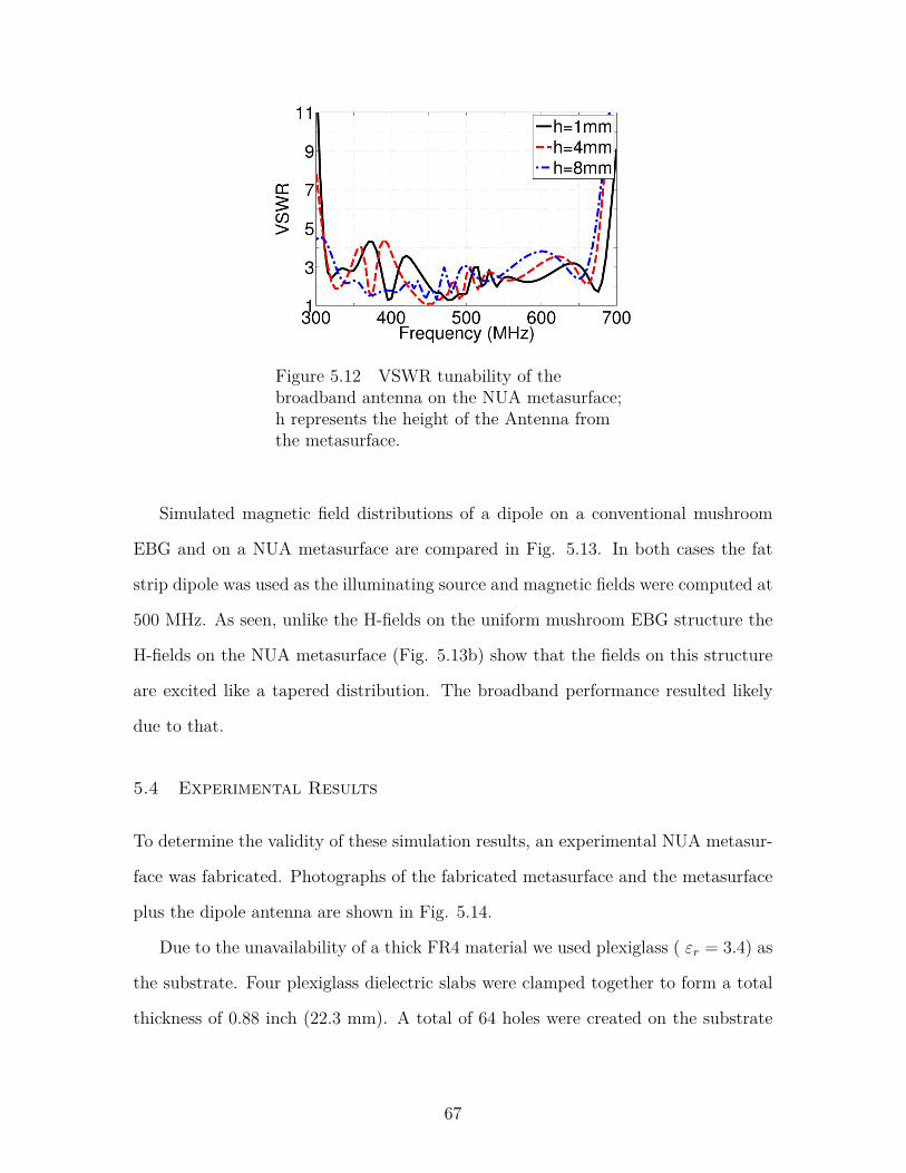
Figure 5.12 VSWR tunability of thebroadband antenna on the NUA metasurface;h represents the height of the Antenna fromthe metasurface.
Simulated magnetic field distributions of a dipole on a conventional mushroom
EBG and on a NUA metasurface are compared in Fig. 5.13. In both cases the fat
strip dipole was used as the illuminating source and magnetic fields were computed at
500 MHz. As seen, unlike the H-fields on the uniform mushroom EBG structure the
H-fields on the NUA metasurface (Fig. 5.13b) show that the fields on this structure
are excited like a tapered distribution. The broadband performance resulted likely
due to that.
5.4 Experimental Results
To determine the validity of these simulation results, an experimental NUA metasur-
face was fabricated. Photographs of the fabricated metasurface and the metasurface
plus the dipole antenna are shown in Fig. 5.14.
Due to the unavailability of a thick FR4 material we used plexiglass ( εr = 3.4) as
the substrate. Four plexiglass dielectric slabs were clamped together to form a total
thickness of 0.88 inch (22.3 mm). A total of 64 holes were created on the substrate
67
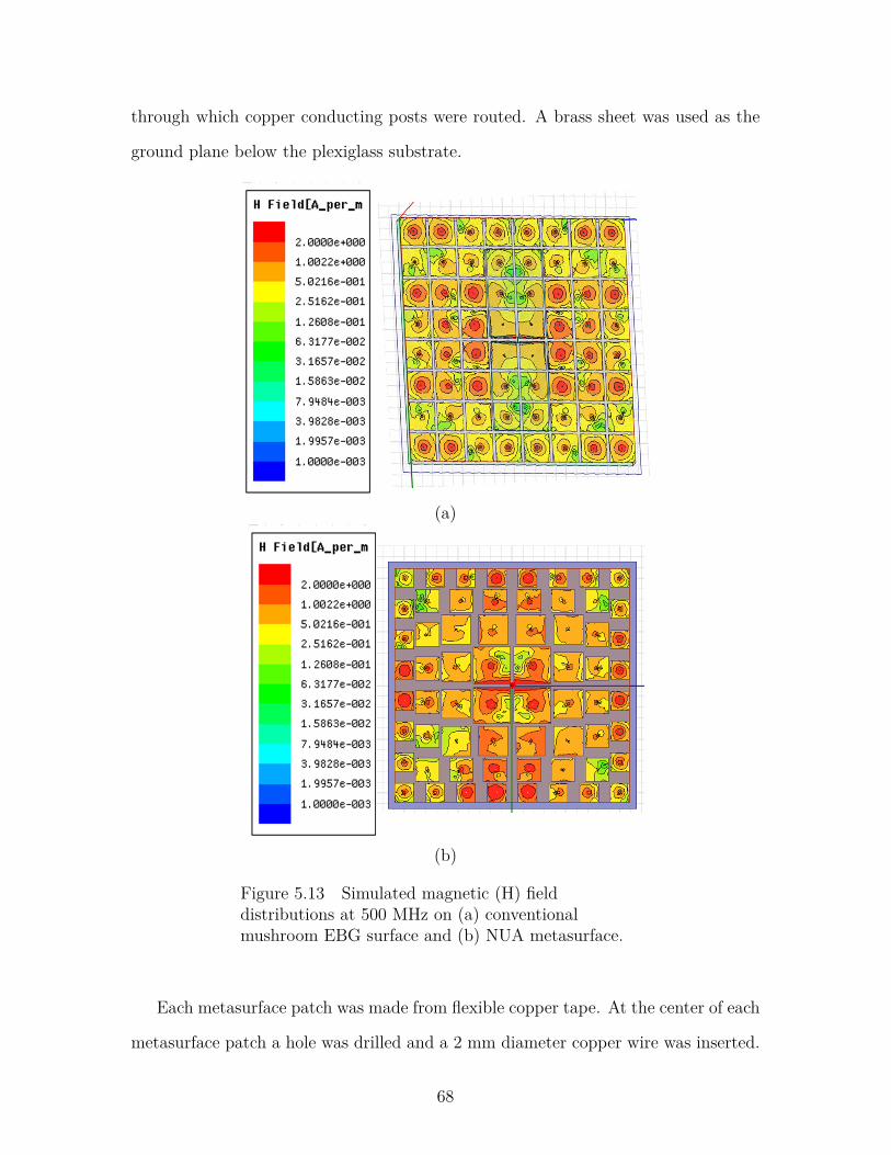
through which copper conducting posts were routed. A brass sheet was used as the
ground plane below the plexiglass substrate.
(a)
(b)
Figure 5.13 Simulated magnetic (H) fielddistributions at 500 MHz on (a) conventionalmushroom EBG surface and (b) NUA metasurface.
Each metasurface patch was made from flexible copper tape. At the center of each
metasurface patch a hole was drilled and a 2 mm diameter copper wire was inserted.
68

(a)
(b)
Figure 5.14 Photographs of (a) the NUAmetasurface and (b) metasurface plusdipole antenna. Total surface area 435mm by 435 mm (17.1 inch by 17.1 inch).
The copper wire was then soldered to the metasurface patch on the top and the brass
ground plane below. Since large brass sheets are heat sinks a heat gun was used along
with a soldering iron to solder the conducting copper wires. The dipole antenna was
also made from flexible copper tape and was placed on a very thin foam material as
shown in Fig. 5.14 . To feed the dipole a semirigid coaxial cable was routed through
the cable and the plexiglass substrate by drilling a large enough hole. The coaxial
cable was connected to a broadband surface mount chip balun (RFXF9503). The
69
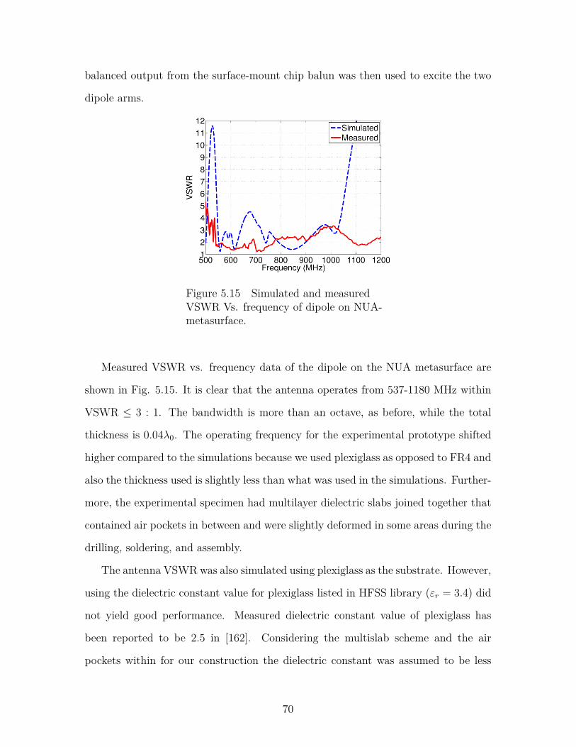
balanced output from the surface-mount chip balun was then used to excite the two
dipole arms.
Figure 5.15 Simulated and measuredVSWR Vs. frequency of dipole on NUA-metasurface.
Measured VSWR vs. frequency data of the dipole on the NUA metasurface are
shown in Fig. 5.15. It is clear that the antenna operates from 537-1180 MHz within
VSWR ≤ 3 : 1. The bandwidth is more than an octave, as before, while the total
thickness is 0.04λ0. The operating frequency for the experimental prototype shifted
higher compared to the simulations because we used plexiglass as opposed to FR4 and
also the thickness used is slightly less than what was used in the simulations. Further-
more, the experimental specimen had multilayer dielectric slabs joined together that
contained air pockets in between and were slightly deformed in some areas during the
drilling, soldering, and assembly.
The antenna VSWRwas also simulated using plexiglass as the substrate. However,
using the dielectric constant value for plexiglass listed in HFSS library (εr = 3.4) did
not yield good performance. Measured dielectric constant value of plexiglass has
been reported to be 2.5 in [162]. Considering the multislab scheme and the air
pockets within for our construction the dielectric constant was assumed to be less
70
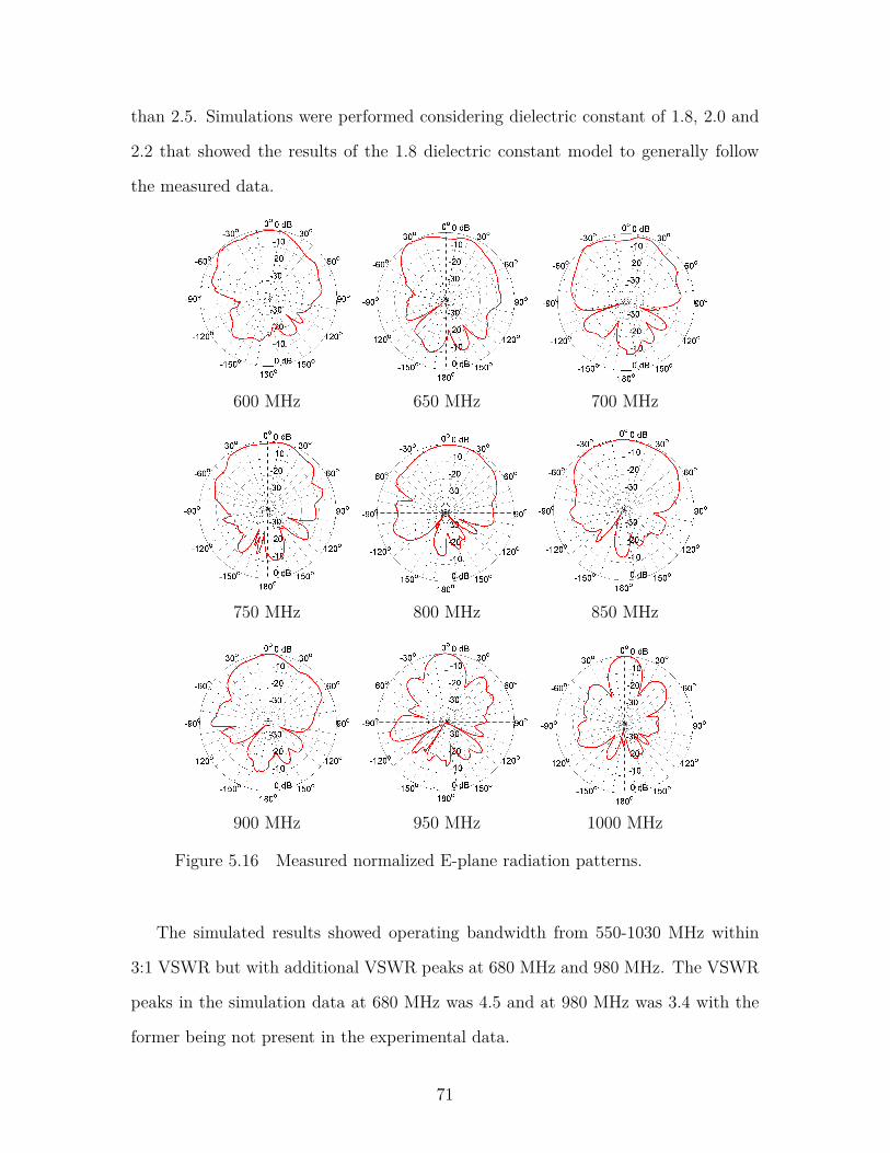
than 2.5. Simulations were performed considering dielectric constant of 1.8, 2.0 and
2.2 that showed the results of the 1.8 dielectric constant model to generally follow
the measured data.
600 MHz 650 MHz 700 MHz
750 MHz 800 MHz 850 MHz
900 MHz 950 MHz 1000 MHz
Figure 5.16 Measured normalized E-plane radiation patterns.
The simulated results showed operating bandwidth from 550-1030 MHz within
3:1 VSWR but with additional VSWR peaks at 680 MHz and 980 MHz. The VSWR
peaks in the simulation data at 680 MHz was 4.5 and at 980 MHz was 3.4 with the
former being not present in the experimental data.
71
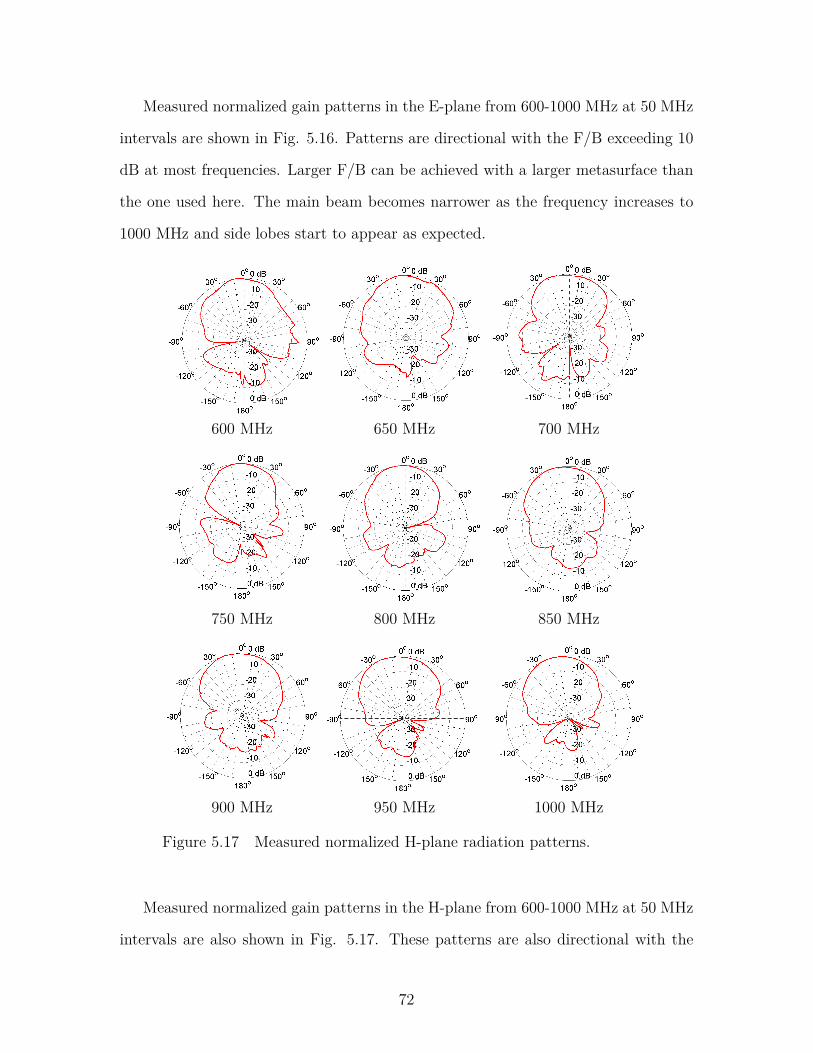
Measured normalized gain patterns in the E-plane from 600-1000 MHz at 50 MHz
intervals are shown in Fig. 5.16. Patterns are directional with the F/B exceeding 10
dB at most frequencies. Larger F/B can be achieved with a larger metasurface than
the one used here. The main beam becomes narrower as the frequency increases to
1000 MHz and side lobes start to appear as expected.
600 MHz 650 MHz 700 MHz
750 MHz 800 MHz 850 MHz
900 MHz 950 MHz 1000 MHz
Figure 5.17 Measured normalized H-plane radiation patterns.
Measured normalized gain patterns in the H-plane from 600-1000 MHz at 50 MHz
intervals are also shown in Fig. 5.17. These patterns are also directional with the
72
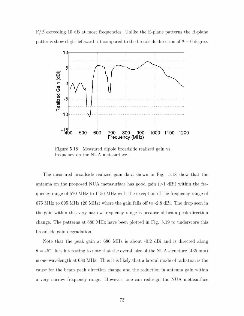
F/B exceeding 10 dB at most frequencies. Unlike the E-plane patterns the H-plane
patterns show slight leftward tilt compared to the broadside direction of θ = 0 degree.
Figure 5.18 Measured dipole broadside realized gain vs.frequency on the NUA metasurface.
The measured broadside realized gain data shown in Fig. 5.18 show that the
antenna on the proposed NUA metasurface has good gain (>1 dBi) within the fre-
quency range of 570 MHz to 1150 MHz with the exception of the frequency range of
675 MHz to 695 MHz (20 MHz) where the gain falls off to -2.8 dBi. The drop seen in
the gain within this very narrow frequency range is because of beam peak direction
change. The patterns at 680 MHz have been plotted in Fig. 5.19 to underscore this
broadside gain degradation.
Note that the peak gain at 680 MHz is about -0.2 dBi and is directed along
θ = 45. It is interesting to note that the overall size of the NUA structure (435 mm)
is one wavelength at 680 MHz. Thus it is likely that a lateral mode of radiation is the
cause for the beam peak direction change and the reduction in antenna gain within
a very narrow frequency range. However, one can redesign the NUA metasurface
73

structure such that the total dimension coincides with the wavelength corresponding
to the frequency at its lower band edge of operation. Radiation patterns at 1050
MHz are also shown in Fig. 5.19 which show that the antenna patterns are generally
satisfactory at this high frequency.
680 MHz (E-Plane) 680 MHz (H-plane)
1050 MHz (E-Plane) 1080 MHz (H-plane)
Figure 5.19 Measured dipole patterns at otherfrequencies (on NUA- metasurface).
5.5 Switched Beam Array on NUA EBG Surface
The NUA EBG concept presented in the earlier sections of this chapter has been
exploited to develop a thin switched beam parasitic array.
5.5.1 Array Configuration
The array geometry shown in Figs. 5.20a and 5.20b shows that it has two parts: an
antenna on Substrate 1 (εr1 and thickness, h) and an EBG structure on Substrate 2
(εr2 and thickness, t).
74

d
W
d
swL swR
DrivenParasitic Parasitic
L lp ld
wp wd th
Ground
Substrate 2
EBG surface
Antenna
Substrate 1
(a) (b)
Y
Z
X
swON
LswOFF
R
Reflection from metal/EBG reflector
Reflection from Parasitic element
Resultant beam
(c)
Figure 5.20 Measured dipole broadside realized gain vs.frequency on the NUA metasurface.
The EBG structure is composed of a frequency selective surface consisting of
square metal patches on a substrate and a ground plane (Fig. 5.20b). The antenna
consists of one driven and two parasitic planar dipole elements (Fig. 5.20a). The
length and width of the driven element are ld and wd, respectively. Similarly the
length and width of each parasitic element are lp and wp, respectively. L and W
represent the total length and width of the array on the EBG. Edge-to-edge separation
between the driven and one of the parasitic dipoles is d. The parasitic elements have
RF switches at their centers (swL and swR in Fig. 5.20a). Array operation can be
explained using [103] and from Fig. 5.20c when there is no EBG and ground plane
present. When only the Left switch (swL) is ON, the left parasitic element operates
as a reflector which directs the array beam to φ = 90 (y-axis). Similarly when only
75

the Right switch (swR) is ON the beam points to φ = 270. When both switches are
ON, the beam points in the forward direction (φ = 0).
5.5.2 Results
First, a three element switched beam antenna array was designed (ld = 57 mm,
wd = 3 mm, lp = 65 mm and d = 20 mm) for operation in free-space at 2.4 GHz. The
array performed as expected. Good return loss and beam steering at 0, 90, and 270
degrees were observed. When the array was placed at a height from a 125 mm square
copper reflector it was found that a separation of at least 18 mm (≈ 0.14λ0 from the
reflector) was required to obtain good return loss. Subsequently the space between
the array and the reflector was filled with Rogers TMM4 (εr = 4.5) substrate. To
ensure that the array still operated at 2.4 GHz its dimensions were adjusted as ld = 18
mm, lp = 18 mm, and d = 18 mm. It was found that a minimum thickness of 11 mm
for the TMM4 was needed for the antenna to have acceptable return loss. Neither of
these approaches seemed feasible or desirable from a practical point of view because
of large thickness.
5.5.2.1 Array on Uniform Planar EBG
Next, array performance was studied on a planar EBG (Fig. 5.21a) structure. The
EBG consisted of 6× 6 square patches on TMM4 substrate (thickness t).
The planar EBG was designed for operation at 2.4 GHz based on the guidelines
found in the literature [163]. The geometrical parameters for the EBG and antenna
were a = 16.3 mm, s = 1.6 mm, h = 1.2 mm, t = 5.8mm, ld = 34.5 mm, lp = 45.5
mm, wd = wp = 3.1 mm, and L = W = 106.8 mm, εr1 = εr2 = 4.5. The smallest
total thickness (h+ t) that allowed good return loss was found to be 7 mm (0.056λ0).
As seen in Fig. 5.21b, |S11| < −10 dB is satisfied at 2.4 GHz for all three switching
combinations with bandwidth being 8%. Fig. 5.21c show the realized gain patterns
76

(a)
(b) (c)
All OFF Left ON Right ON
Figure 5.21 (a)Top view of a uniform EBG, (b) |S11| Vs.frequency, and (c) azimuth plane (xy) pattern.
at 2.4 GHz in the azimuth (XY) plane. The array can steer its beam in the azimuth
plane at 0, 30, and 330 for three switching cases: all OFF (All OFF is needed in
the presence of the EBG to direct the beam in the forward direction), Left ON and
Right ON, respectively. The F/B is 12 dB. Peak gains are 8 and 6.7 dBi for all OFF
and one (either Left or Right) ON, respectively.
77
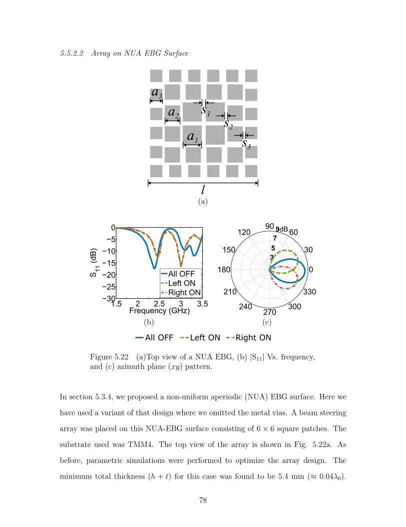
5.5.2.2 Array on NUA EBG Surface
(a)
(b) (c)
All OFF Left ON Right ON
Figure 5.22 (a)Top view of a NUA EBG, (b) |S11| Vs. frequency,and (c) azimuth plane (xy) pattern.
In section 5.3.4, we proposed a non-uniform aperiodic (NUA) EBG surface. Here we
have used a variant of that design where we omitted the metal vias. A beam steering
array was placed on this NUA-EBG surface consisting of 6× 6 square patches. The
substrate used was TMM4. The top view of the array is shown in Fig. 5.22a. As
before, parametric simulations were performed to optimize the array design. The
minimum total thickness (h + t) for this case was found to be 5.4 mm (≈ 0.04λ0).
78

This is more than 50% thickness reduction from the array above conductive ground
with a TMM4 substrate. The geometrical parameters for this case were a1 = 14.4
mm, a2 = 11.5 mm, a3 = 9.2 mm, s1 = 1.44 mm, s2 = 1.15 mm, s3 = 0.92 mm,
h = 1.4 mm, t = 4.0 mm, ld = 32.1 mm, lp = 41.8 mm, wd = wp = 3.2 mm, and
L = W = 75.8 mm.
As seen in Fig. 5.22b, |S11| < −10 dB is satisfied at 2.4 GHz for all three switching
combinations. Fig. 5.22c shows that the array can steer its beam in the azimuth plane
at 0, 25, and 335 for three switching combinations: all OFF, Left ON and Right
ON respectively. The (F/B) is very high for this case, nearly 30 dB. Peak gain is 8.4
dBi when all switches are OFF and 7 dBi when only one switch is ON.
79

Chapter 6
Low Cost Bidirectional Series-fed Phased
Array for Body-Centric Wireless
Communications
6.1 Introduction
In recent years, high gain body wearable antennas are drawing attention of researchers
as trans-receiving solution for first responders, astronauts, soldiers, and law enforce-
ment personnel.
In Chapters 3, 4, and 5 we presented three switched beam parasitic antenna arrays.
Although the arrays are low cost and efficient, they suffer from wide overlapping
beams (90 − 120). Traditional phased arrays can produce narrow beams but have
large footprints making them unsuitable for wearable applications. As stated in
section 2.4, a bidirectional series-fed phased array can be a good alternative.
In this chapter we present the design and development of a varactor controlled
bidirectional series-fed array. Four series-connected driven dipoles and eight parasitic
dipole elements form a high gain array where patterns are configured using a phase
shifter that can add tunable progressive phases. The phase shifter is implemented
using unequal line length couplers connected to varactor diodes. The ground plane
of the phase shifter serves as a reflector which improves the directivity of the array,
reduces RF exposure and isolates the antenna from the phase shifter and the bias
network. By incorporating dc bypass lines within the microstrip feedline, the com-
80

plexity of implementing a biasing network is resolved making it possible to use a
single bias tee to bias all varactors. The design frequency is selected to be 5.2 GHz
but implementation at other frequencies is also possible.
6.2 Proposed Array Configuration
Phase shifter
Copper ground plane
Foam spacer
Drivenelements
Parasiticelements
Through holefor dipole feed
Layer 1
Layer 2
Layer 3
Layer 4
Figure 6.1 Array configuration.
The configuration of the proposed bidirectional series-fed antenna array is shown
in Fig. 6.1. The entire antenna array consists of four layers. There are four sub-
arrays interconnected with three phase shifters. Each subarray consists of two shorted
parasitic v-dipoles and a driven dipole. The parasitics are located on the top layer,
and the driven elements are on layer 2. These are constructed on two different
substrate boards. Layer 3 and layer 4 can be constructed using a two sided substrate
board where layer 3 is the ground plane, and the bottom layer or layer 4 contains
the phase shifter network. Two vertical poles (cylindrical copper wires) from the feed
region of the phase shifter goes through a hole in the ground and connects in the feed
region of the dipole.
81
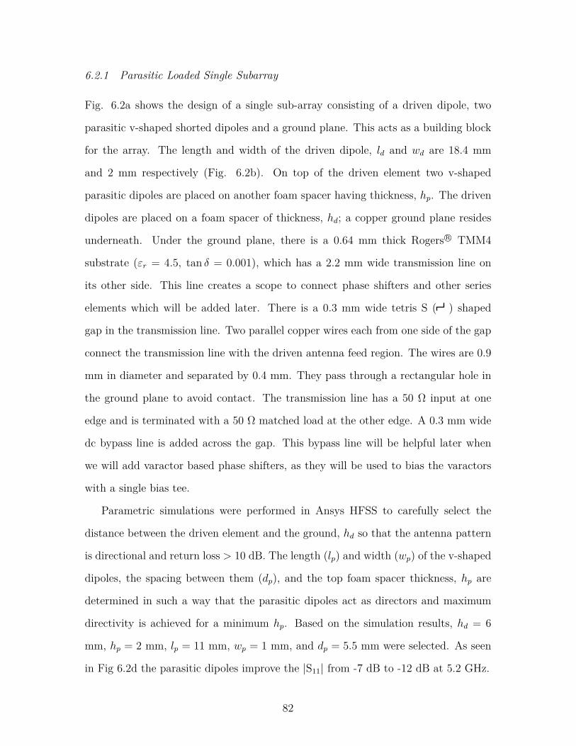
6.2.1 Parasitic Loaded Single Subarray
Fig. 6.2a shows the design of a single sub-array consisting of a driven dipole, two
parasitic v-shaped shorted dipoles and a ground plane. This acts as a building block
for the array. The length and width of the driven dipole, ld and wd are 18.4 mm
and 2 mm respectively (Fig. 6.2b). On top of the driven element two v-shaped
parasitic dipoles are placed on another foam spacer having thickness, hp. The driven
dipoles are placed on a foam spacer of thickness, hd; a copper ground plane resides
underneath. Under the ground plane, there is a 0.64 mm thick Rogers R© TMM4
substrate (εr = 4.5, tan δ = 0.001), which has a 2.2 mm wide transmission line on
its other side. This line creates a scope to connect phase shifters and other series
elements which will be added later. There is a 0.3 mm wide tetris S ( ) shaped
gap in the transmission line. Two parallel copper wires each from one side of the gap
connect the transmission line with the driven antenna feed region. The wires are 0.9
mm in diameter and separated by 0.4 mm. They pass through a rectangular hole in
the ground plane to avoid contact. The transmission line has a 50 Ω input at one
edge and is terminated with a 50 Ω matched load at the other edge. A 0.3 mm wide
dc bypass line is added across the gap. This bypass line will be helpful later when
we will add varactor based phase shifters, as they will be used to bias the varactors
with a single bias tee.
Parametric simulations were performed in Ansys HFSS to carefully select the
distance between the driven element and the ground, hd so that the antenna pattern
is directional and return loss > 10 dB. The length (lp) and width (wp) of the v-shaped
dipoles, the spacing between them (dp), and the top foam spacer thickness, hp are
determined in such a way that the parasitic dipoles act as directors and maximum
directivity is achieved for a minimum hp. Based on the simulation results, hd = 6
mm, hp = 2 mm, lp = 11 mm, wp = 1 mm, and dp = 5.5 mm were selected. As seen
in Fig 6.2d the parasitic dipoles improve the |S11| from -7 dB to -12 dB at 5.2 GHz.
82

Parasitic elementsFoam spacer
Driven dipole
Foam spacer
Copper groundCopper wire
Highly resistive line50Ω loadTransmission lineSubstrate
Input
hp
hd
t
(a)
wd
ld lp
wp
dp
(b) (c)
Frequency (GHz)4.5 5 5.5 6
S11
(dB
)
-20
-15
-10
-5
0
With parasiticWithout parasitic
-5
0
5
10
90
60
300
-30
-60
-90
-120
-150180
150
120
With parasiticWithout parasitic
dB
(d) (e)
Figure 6.2 (a) Configuration of a single sub array, (b) dimensions of asingle driven dipole, (c) dimensions of a parasitic element, (d) |S11| vs.frequency for the single subarray and (e) Realized gain pattern in theyz plane at 5.2 GHz.
The parasitic elements also enhance the gain by 2 dB which is apparent in Fig.
6.2e that shows the realized gain patterns in the yz plane at 5.2 GHz. For both cases,
83

with parasitic and without, the beam is directed to θ = 0 and peak gains are 6.4
dBi and 4.2 dBi respectively.
6.2.2 Phased Array Formation
To examine the effect of progressive phase, HFSS simulations were conducted forming
a four element array using the sub-array developed in the previous section. Fig. 6.3a
shows the cross-sectional view of the formation.
Input 1 Input 2 Input 3 Input 450ΩterminationTansmissionline
d
Ground planeCopper wire
Parasiticelement
Drivenelement
Foam spacer
(a)
Frequency (GHz)4.5 5 5.5 6
Snn
(dB
)
-20
-15
-10
-5
0
S11
S22
S33
S44
24681012
90
60
300
-30
-60
-90
-120
-150180
150
120
β=0°β=90°β=-90°
dB
(b) (c)
Figure 6.3 (a) Cross-sectional view (yz plane) of the array, (b) Snn vs.frequency, and (c) realized gain pattern in yz plane at 5.2 GHz for threeprogressive phases.
The center to center distance, d between two consecutive subarrays is 33.8 mm.
Total dimensions of the ground plane is 53.8× 145.8 mm2. For this study each sub-
84
array has a separate input source (Fig. 6.3a) so that the progressive phase, β can be
controlled independently for each port in HFSS. Simulated return losses, (|Snn|) vs
frequency at all ports are plotted in Fig. 6.3b. At 5.2 GHz, the |Snn|n=1,2,3,4 < −12
dB. The 10-dB |Snn| bandwidth of this array is about 500 MHz as it operates from
5.12 GHz to 5.65 GHz.
Fig. 6.3c shows the simulated radiation pattern of the array in the yz plane for
consecutive phase shifts of β = 0, 90 and −90. As d = 33.8 mm and λ = 57.7
mm is known, one can calculate from the relation θm = − sin−1(λβ/2πd) that for
β = 0, 90, and−90, the maximum beams should occur at θm = 0, −25, and 25,
respectively. This is in concordance with our observations from Fig. 6.3c. The peak
realized gain of the array is 11.2 dBi for all the cases. In practice, to implement these
progressive phases a shift shifter needs to be designed which is described in the next
section.
6.2.3 Phase Shifter Design
Recently several authors [71, 164] have proposed phase shifters based on unequal line
length coupler with reflective load. The phase shifter designed and implemented in
this work was adapted from [164]. The schematic is shown in Fig. 6.4a.
The phase shifter was simulated on a 0.64 mm Rogers TMM4 substrate (εr = 4.5,
tan δ = 0.001) in Ansys HFSS. Fig. 6.4b shows an unequal line length coupler with
its key parameters. The characteristic impedances Z1 and Z2 govern the width of
their corresponding microstrip line-sections. Once the width is known, equivalent
permittivity and hence the guided wavelength can be calculated which is used to find
the lengths of the sections from the delays θ1 and θ2. Equations (6.1) - (6.4) can be
used to calculate these parameters. The design starts with choosing a power division
ratio and finding the constant, k in Equation (6.1). Width (or the charcteristic
impedance) of one line is selected and the width of the other line can be determined
85

using Equation (6.2). Its parameters θ1 and θ2 can be computed from (6.3) and (6.4).
In our design (Fig. 6.4a), the parameters w3, w4, lc, and le were determined using
these relations.
lps
la lc
w2
w1
w4
w3
rs
w6
w7
lb
ld
lew5
PORT 2
PORT 3PORT 4
PORT 1
Z2, θ2
Z1, θ1
(a) (b)
Figure 6.4 (a) Geometry of a single phase shifter and (b) an unequallength branchline coupler.
∣∣∣∣∣S21
S31
∣∣∣∣∣2
= k2
1− k2 (6.1)
1Z2
1− 1Z2
2= 1Z2
0(6.2)
Z2| sin θ2| = Z0k√
1− k2(6.3)
Z1 tan θ1 = −Z2 tan θ2 (6.4)
As seen in 6.4a, the coupled port (port 3) and the isolated port (port 4) of the
coupler are connected with radial stubs through varactor diodes. The radial stubs
were designed following the guideline provided in [71]. The stubs are shorted to the
ground plane as they ensure broader range of phase shift. The geometrical parameters
of the phase shifter are listed in Table 6.1.
86

Table 6.1 Geometry parameters for the phase shifter (in mm).
Parameters w1 w2 w3 w6 w5 w6 w7Values (mm) 2.24 1.9 1 2.5 2.5 7.83 1.9Parameters lps la lb lc ld le rsValues (mm) 33.8 13.5 1.5 3.7 1.83 9 6
Frequency (GHz)4.5 5 5.5 6
S11
(dB
)
-30
-25
-20
-15
-10
-5
0
(a)
Frequency (GHz)4.5 5 5.5 6
S21
(dB
)
-30
-25
-20
-15
-10
-5
0
Frequency (GHz)4.5 5 5.5 6
S21
(de
gree
)
-180-135
-90-45
04590
135180
0.2 pF 0.6 pF 1.0 pF 1.4 pF 1.8 pF 2.2 pF
(b) (c)
Figure 6.5 (a) S11 vs. frequency, (b) S21 vs. frequency, and (c) S11 phasevs. frequency for different capacitance values.
By varying the bias voltage, the varactor capacitance can be changed. This ca-
pacitance in tandem with the radial stubs change the load impedances at the coupled
port (port 3 in Fig. 6.4) and the isolated port (port 4). This load impedance variation
in ports 3 and 4, by the principle of branchline couplers, causes a phase shift between
87

port 1 and port 2 which is reflected in the S21 phase. In HFSS, the varactor diodes
were modeled as ideal lumped element capacitors.
Return loss performance |S11|(dB) vs frequency for different varactor capacitance
values are plotted in Fig. 6.5a. The varactor capacitance, C is varied from 0.2 pF
to 2.2 pF with 0.4 pF interval. It is observed that for C < 0.6 pF, the return loss is
> −6 dB at 5.2 GHz. For higher capacitance values, |S11| < −10 dB at 5.2 GHz.
Fig. 6.5b shows the simulated insertion loss performances vs frequency varying C
from 0.2 pF to 2.2 pF with 0.4 pF interval. Again, for C = 0.2, 0.6, 1.0, 1.4, 1.8, , and 2.2
pF |S21| are -22, -0.9, -0.4, -0.4, and -0.6 dB, respectively. Therefore, higher capaci-
tance values are suitable for our design due to low insertion loss. Fig. 6.5c shows the
effect of capacitance values on S21 phases. As capacitance varies from 0.2 to 2.2 pF,
S21 phase varies from 134 to −123 which suggests that around 250 degrees of phase
shifting is possible with this shifter.
6.2.4 Bidirectional Series-fed Array
Next, a four element series fed array was modeled in HFSS including three phase
shifters. The varactors were modeled as lumped capacitors. First the array was fed
from left. Here the phrase ‘fed from left’ implies that port 1 is excited and port 2
is terminated with a matched load. Similarly, ‘fed from right’ implies that port 2 is
excited and port 1 is terminated with a matched load.
In this study, three capacitance values were considered for the varactor: 0.6 pF,
1 pF, and 2.2 pF. The simulated S11 vs. freq. and the realized gain pattern in the yz
plane at 5.2 GHz are shown in Fig. 6.6. From Fig. 6.6a we observe that |S11| < −10
dB at 5.2 GHz for all three capacitance values. Fig. 6.6b shows the realized gain in
the yz plane for C = 2.2 pF and C = 0.6 pF.
88
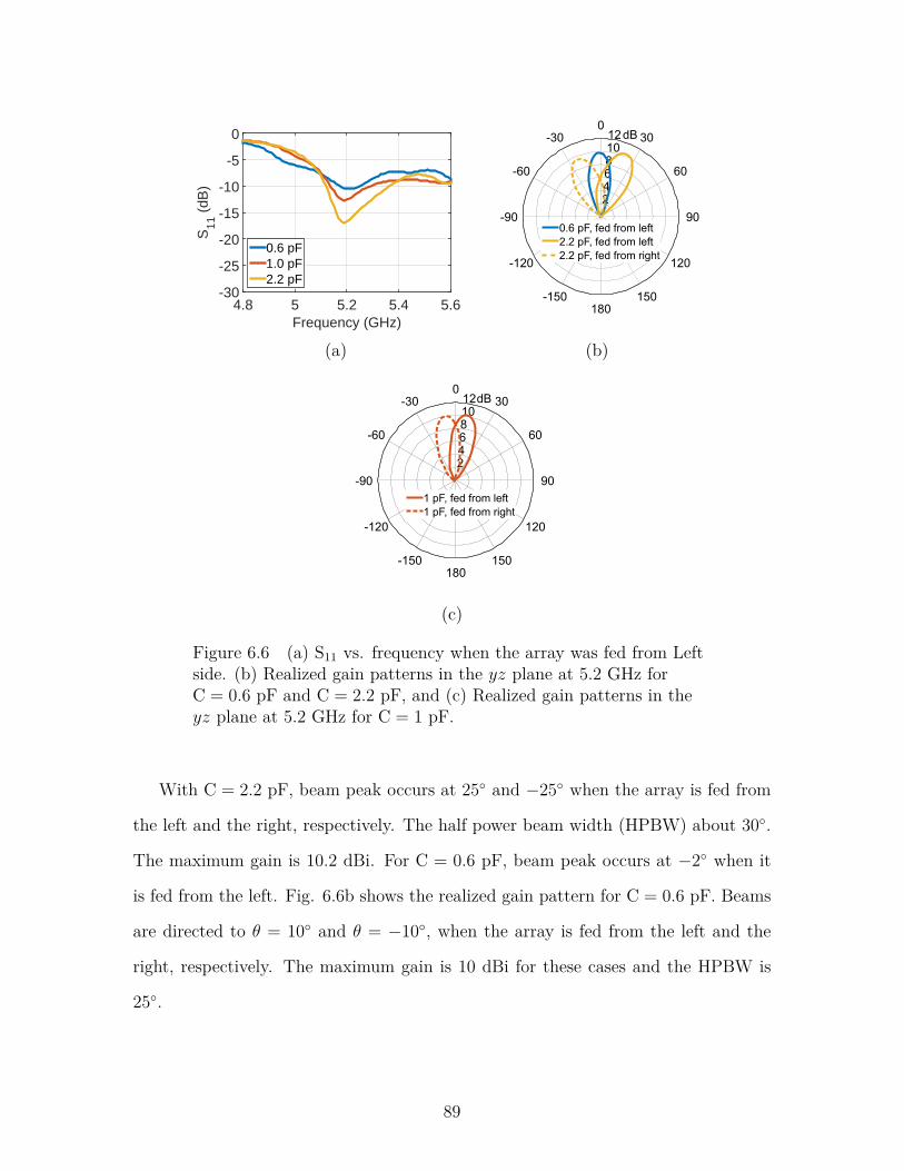
Frequency (GHz)4.8 5 5.2 5.4 5.6
S11
(dB
)
-30
-25
-20
-15
-10
-5
0
0.6 pF1.0 pF2.2 pF
24681012
90
60
300
-30
-60
-90
-120
-150180
150
120
0.6 pF, fed from left2.2 pF, fed from left2.2 pF, fed from right
dB
(a) (b)
24681012
90
60
300
-30
-60
-90
-120
-150180
150
120
1 pF, fed from left1 pF, fed from right
dB
(c)
Figure 6.6 (a) S11 vs. frequency when the array was fed from Leftside. (b) Realized gain patterns in the yz plane at 5.2 GHz forC = 0.6 pF and C = 2.2 pF, and (c) Realized gain patterns in theyz plane at 5.2 GHz for C = 1 pF.
With C = 2.2 pF, beam peak occurs at 25 and −25 when the array is fed from
the left and the right, respectively. The half power beam width (HPBW) about 30.
The maximum gain is 10.2 dBi. For C = 0.6 pF, beam peak occurs at −2 when it
is fed from the left. Fig. 6.6b shows the realized gain pattern for C = 0.6 pF. Beams
are directed to θ = 10 and θ = −10, when the array is fed from the left and the
right, respectively. The maximum gain is 10 dBi for these cases and the HPBW is
25.
89

6.2.5 Array with Fabric Materials
(a) (b)
(c) (d)
Figure 6.7 Simulation results for array on fabric substrate.
To consider wearable applications, a textile-based array was modelled and simulated.
Instead of TMM4, a cotton substrate (εr = 1.6, tan δ = 0.001) was used. The driven
dipoles, parasitic dipoles, ground, and the phase shifters were modeled using copper
taffeta (surface resistivity = 0.05 Ω/sq.)
Return loss and realized gain patterns at 5.2 GHz were studied for two different
capacitance values: 0.6 pF and 2.8 pF. From Figs. 6.7a and 6.7b, we see that, for
C = 0.6 pF, the return loss is near -10 dB and beam steering is possible at −30 and
30. From Figs. 6.7c and 6.7d we see that, for C = 2.8 pF, beam peaks occur at
−15 and 15, when fed from left and right.
90
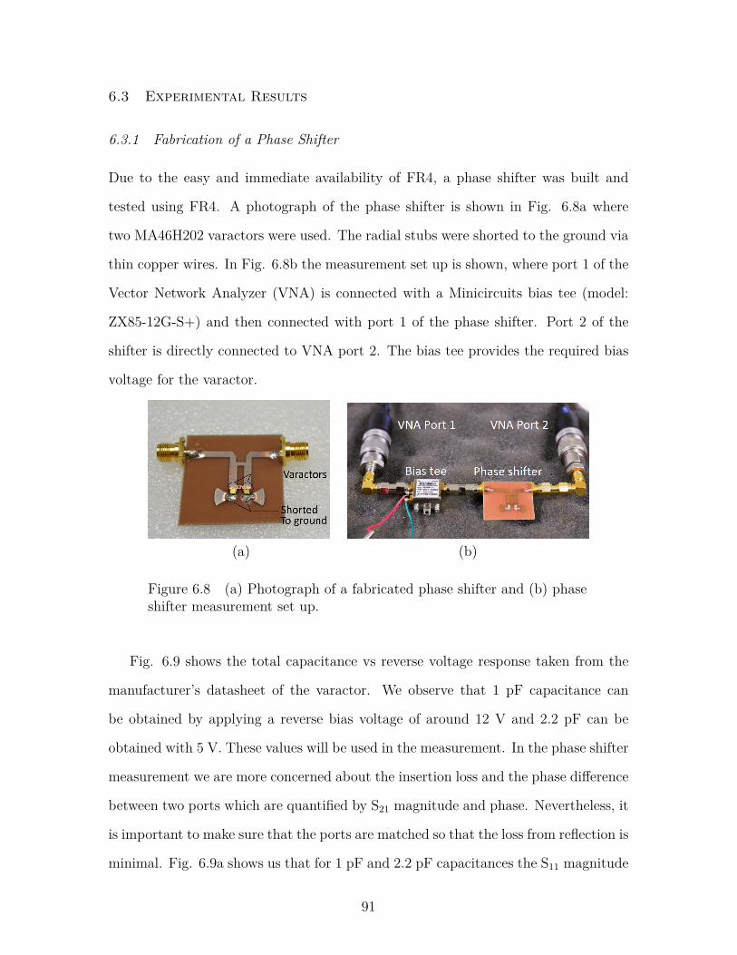
6.3 Experimental Results
6.3.1 Fabrication of a Phase Shifter
Due to the easy and immediate availability of FR4, a phase shifter was built and
tested using FR4. A photograph of the phase shifter is shown in Fig. 6.8a where
two MA46H202 varactors were used. The radial stubs were shorted to the ground via
thin copper wires. In Fig. 6.8b the measurement set up is shown, where port 1 of the
Vector Network Analyzer (VNA) is connected with a Minicircuits bias tee (model:
ZX85-12G-S+) and then connected with port 1 of the phase shifter. Port 2 of the
shifter is directly connected to VNA port 2. The bias tee provides the required bias
voltage for the varactor.
(a) (b)
Figure 6.8 (a) Photograph of a fabricated phase shifter and (b) phaseshifter measurement set up.
Fig. 6.9 shows the total capacitance vs reverse voltage response taken from the
manufacturer’s datasheet of the varactor. We observe that 1 pF capacitance can
be obtained by applying a reverse bias voltage of around 12 V and 2.2 pF can be
obtained with 5 V. These values will be used in the measurement. In the phase shifter
measurement we are more concerned about the insertion loss and the phase difference
between two ports which are quantified by S21 magnitude and phase. Nevertheless, it
is important to make sure that the ports are matched so that the loss from reflection is
minimal. Fig. 6.9a shows us that for 1 pF and 2.2 pF capacitances the S11 magnitude
91

is < -10 dB at 5.2 GHz, which is satisfactory. Similarly S22 magnitude was observed
and found satisfactory.
In Fig. 6.9b measured insertion loss for bias voltages 12 V and 5 V are shown. In
the measurement there was a 0.7 dB extra loss for the bias tee which has been de-
embedded in these figures. We observe that for 12 V bias voltage (which is equivalent
to varactor capacitane, C = 1 pF), the insertion loss is 2.4 dB at 5.2 GHz. In the
simulation with 1 pF capacitor we have observed an insertion loss of 1.4 dB (see Fig.
6.9c, with Rs=0 Ω), which is 1 dB less than what we observe in the measurement.
This discrepancy can be explained using a series resistance which is mentioned in the
equivalent circuit of the varactors provided by the manufacturer.
As the value of this series resistance, Rs was not specified in the device datasheet,
we ignored it in the initial simulation. But Rs shows its effect when we measure the
two-port S-parameter data. To study the effect of this series resistance, we performed
a parametric simulation from Rs = 0 to 5 Ω with 1 Ω interval. Fig. 6.9d shows the
simulated S21 of the phase shifter with variation of series resistance, Rs. For Rs = 2Ω
and 3Ω, insertion losses of 2.1 dB and 2.4 dB are observed. The 1 dB higher insertion
loss in the measurement is likely due to the effect of this 3 Ω resistance.
Fig. 6.9e shows the phase shifting behavior with the change of the bias voltage.
We observe that for 12 V and 5 V bias voltages, the measured S21 phases at 5.2 GHz
are 127 and 157, respectively. The measured phase values do not directly agree with
the simulation (−54 and −87 for 1 pF and 2.2 pF capacitances). This is because
the measurement includes the phase from the bias tee. As the bias tee phase is the
same for both cases, its effect can be canceled out if we consider the difference of S21
phases for 1 pF and 2.2 pF cases. One can calculate that the difference is 30 for
measurement and 33 for simulation, which is in close agreement.
92

0.1
1
10
100
0.1 1 10 100
Tota
l Ca
pa
cita
nce
(p
F)
Reverse Voltage (V)
MA46H202
Frequency (GHz)4.8 5 5.2 5.4 5.6
S11
(dB
)
-30
-25
-20
-15
-10
-5
0Sim. 1 pFMeas. 12 V (~1 pF)Sim. 2.2 pFMeas. 5 V (~2.2 pF)
(a) (b)
Frequency (GHz)4.8 5 5.2 5.4 5.6
S21
(dB
)
-6
-5
-4
-3
-2
-1
0
-3.52
-2.40
Meas. 12 V (~1 pF)Meas. 5 V (~2.2 pF)
Frequency (GHz)4.8 5 5.2 5.4 5.6
S2
1(d
B)
-6
-5
-4
-3
-2
-1
0
Sim. with C = 1 pF
Rs=0 ΩRs=1 ΩRs=2 ΩRs=3 ΩRs=4 Ω
(c) (d)
Frequency (GHz)4.8 5 5.2 5.4 5.6
S21
(de
gree
)
-180
-120
-60
0
60
120
180
-157
-127
-54-87
Sim. 1 pFMeas. 12 V (~1 pF)Sim. 2.2 pFMeas. 5 V (~2.2 pF)
Frequency (GHz)4.8 5 5.2 5.4 5.6
S21
(dB
)
-6
-5
-4
-3
-2
-1
0
-1.44
-0.57
C = 1 pFSim. with FR4Sim. with TMM4
(e) (f)
Figure 6.9 (a) Photograph of a fabricated phase shifter, (b) measured S11, (c)measured S21, and (d) measured S21 phase of the shifter.
On a related note, it should be noted that even with Rs = 0 Ω the 1.4 dB insertion
93

loss in each phase shifter can have detrimental effect on the total array gain. Bulk
of this loss is due to the loss tangent of FR4 substrate (tan δ = 0.02), which can be
reduced by using a low loss material such as TMM4 (tan δ = 0.001). In Fig. 6.9f the
comparison of simulated |S21| between FR4 and TMM4 are shown. It is clear that
the insertion loss for TMM4 is almost 1 dB less than that for FR4. This led us to
switch from FR4 to TMM4 substrate for the entire array simulation and fabrication.
6.3.2 Array Fabrication and Return Loss Measurement
A prototype of the array shown in Fig. 6.1 was built using TMM4 substrate and
measured for S parameters. Fig. 6.10a shows a photograph of the top layer of the
array which contains the parasitic elements. The parasitic elements were made using
flexible copper tapes and placed on a 2 mm thick Rohacell R© foam spacer with an
area of 34 × 144 mm2. The driven elements (not shown in photographs as they are
concealed by the top layer) were also made using copper tapes and placed on a 6
mm thick Rohacell foam sheet. Layer 3 which contains the ground and layer 4 which
has the phase shifter network (see Fig. 6.1) are built on the two sides of a 0.64 mm
thick TMM4 substrate. Fig. 6.10b depicts the bottom layer (layer 4) of the array,
from where a phase shifter network with three phase shifters can be seen. A total
of six MA46H202 varactors (two for each shifter) were used which were connected
to the phase shifter using conductive epoxy. Each phase shifter has two radial stubs
which are shorted to the ground via 0.9 mm diameter copper wires. As seen in the
figure, there are four feed regions in the phase shifter network. From each feed region
two 0.9 mm diameter copper wires go through a hole in the ground, get accross the
foam spacer and connect with two arms of a driven dipole. For the experiment the
left port was connected with a Minicircuits bias tee through an adapter and then
connected with one port of the VNA. The right port was terminated with a standard
50 Ω coaxial load.
94

(a)
(b)
Frequency (GHz)4.8 5 5.2 5.4 5.6
S11
(dB
)
-14
-12
-10
-8
-6
-4
-2
0
5 V12 V
(c)
Figure 6.10 Photograph of the (a)top layer ofthe array with parasitic elements and (b)bottom later of the array containing the phaseshifter network, and (c) measured |S11| vs.frequency for two different bias voltages.
As different bias voltages were applied shift in the S11 magnitude was observed.
Fig. 6.10c shows the S11 vs frequency of the array for 5 V and 12 V bias voltages.
Ideally these voltages should translate into varactor capacitances of 2.2 pF and 1
95

pF respectively. Comparing the measured S-parameter data with the simulated S-
parameter data from Fig. 6.6a, it can be seen that the resonant frequency has shifted
from 5.2 GHz to 5.4 GHz. The 10 dB bandwidth is ≈20 MHz. The minor shift can
be attributed to imperfections in the fabrication process.
The driven and parasitic elements were manually cut from copper tapes where
variation in length and width may have occurred. The wires that connect the phase
shifter with the driven element should ideally be separated by 0.4 mm, but this
separation could not be guaranteed during fabrication. In the simulation model there
was no air gap between the two foam spacers or between the foam spacer and the
ground plane. Practically it was not possible to ensure that. Also there might be
some non-ideality in the substrate which could have caused the substrate dielectric
constant to be different than the ideal value used in the simulation. The shift in
frequency can be a combined effect of all these artifacts.
96
Chapter 7
Conclusion and Future Work
7.1 Conclusion
In this dissertation, several innovative techniques to design high gain pattern recon-
figurable antenna arrays for portable and wearable applications are presented. A
comparative study among different methods for beam steering reveals that the tradi-
tional phased array technique is incompatible for portable handheld and body-worn
array designing as it requires large space, long delay lines, and complicated bias net-
works. The switched beam parasitic array is a viable approach where very small
antenna volumes are available. Cases where moderate amount of space is available,
varactor controlled series-fed arrays are attractive because they can provide narrow
beamwidth in the steering plane allowing well defined nulls between consecutive pat-
terns. The series-fed array is more appropriate for wearable applications. Below are
the principal conclusions.
First, using the switched beam parasitic array technique, a 4-subarray collinear
pattern reconfigurable smart antenna array was designed, developed and tested val-
idating performance. Simulation results in both free-space and on FR4 show that
the array operates at around 5 GHz with better than 10 dB return loss and better
than 17 dB mutual coupling. For the FR4 array, the peak gain is between 9.7-11
dBi for the three different reconfiguration angles, e.g. 0, 70 and 290 degrees. Ex-
perimental fabrication and tests show that the array meets the input |Snn| and |Smn|
characteristics of <-10 dB and <-15 dB, respectively. Measured pattern results show
97
the pattern reconfiguration in three different angles in the azimuth albeit with some
degradation due to the presence of long DC bias wires. Measured peak gain is about
1 dB lower than the simulated gain. The reflections and distortions in the pattern
can be largely eliminated by the use of lumped element baluns and dc bias traces
made from materials with high sheet resistance (>500 Ω/square for instance) as op-
posed to standard copper wires. However, in that case instead of PIN diodes that are
current (mA) controlled varactor diodes or RF MEMS switches should be used that
almost conducts no current (<nA). Finally, when the radiation properties and gain
results were used in system level simulations it was found that the high-gain pattern
reconfigurable antenna array provided 59% increase in SINR over an omnidirectional
antenna.
Next, a high-gain collinear MIMO antenna array design is presented for body-
worn wireless application. For three switching states the array beam directions can be
steered into three different directions. Array performance for various conductive and
nonconductive fabric materials is investigated. Array on a curvature and array near
a phantom are studied. The half-power beamwidth is very narrow in the elevation
plane (approximately 20). The array gain is 12.3 dBi for a 4 sub-array embodiment
near a phantom. The experimental data with loss tangent measurement is presented.
Then, the concept of a Non-Uniform Aperiodic (NUA) metasurface is studied in
the context of achieving broad dipole antenna bandwidth while the total structure
thickness is kept less than 0.05λ0. The frequency range selected is the UHF frequency
band because there are many commercial and military applications that may benefit
from the outcomes of this research. Starting from a scaled design of a strip dipole on
a uniform mushroom EBG structure, the study progressed into tapered metasurface
structures that focused on both increasing and decreasing tapers. In either case, the
total volume of the metasurface was kept constant as that of the uniform EBG but the
individual patch dimensions and their interelement spacing were varied according to a
98

percent taper. This was inspired by the principles of broadband impedance matching
using multisection quarter wave transformers with differing (tapered) characteristic
impedances. Except for our case, the dipole is the illuminating source that needed
to be matched to the EBG surface underneath it.
It was observed that with an increasing taper i.e. when the metasurface started
with smaller patch sizes and interelement distances at the center and then grew radi-
ally outward, the outcome was not desirable meaning that dipole antenna bandwidth
actually degraded. Conversely, when the metasurface started with larger patch sizes
and interelement distances at the center and then decreased radially, the outcome was
broad dipole antenna bandwidth. An experimental prototype fabricated and tested
clearly show that the proposed metasurface plus antenna concept can provide one oc-
tave pattern and gain bandwidth with a total thickness of 0.05λ0. This was achieved
without any magnetic material loading or frequency reconfiguration using electronic
devices. Using a scaled and refined version of the NUA EBG surface designed for UHF
range, a thin high-gain EBG-based pattern reconfigurable array design is presented
for 2.4 GHz wireless application. The effects of array thickness on its performance
are investigated and the thickness limits have been determined for several types of
reflectors. With a non-uniform planar EBG structure the array thickness can be re-
duced by more 50% of that of an array on conductive ground plane. With a thickness
of only 0.04λ0, the array can steer its beam in three distinct directions in the azimuth
plane. The array peak gain is 8.4 dBi, average beamwidth is 60and F/B is 30 dB.
Finally, the design of a varactor controlled bidirectional series-fed array is pre-
sented. A phase shifter was designed with varactor controlled unequal line length
branchline coupler. Simulation data show beam steering from −25 to 25 with 10.2
dBi peak gain. The array beamwidth in the steering plane is narrow: 25 − 30. A
fabric based design was presented which can be integrated with clothing of emer-
gency personnel. Experimental results show promises for the applicability of the
99
phase shifter.
7.2 Future Work
The beam steering MIMO array for handheld devices investigated in Chapter 3 con-
tains four subarrays. By increasing the number of subarrays, higher gain and lower
elevation plane beamwidth can be obtained. The array can be made more compact
by following multiple strategies such as using folded dipoles as driven elements, using
dielectric filler materials inside the cavity of the array, optimizing antenna element
dimensions using advanced algorithms such as genetic algorithm, particle swarm op-
timization, etc. The losses in array gain and deviation in pattern can be reduced by
adopting some useful techniques such as building the antenna elements on low-loss
substrates, using lumped element baluns, making dc bias traces from materials with
high sheet resistance which would reduce field interaction with bias network, and by
using voltage controlled devices such as varactor diodes, MEMS switches, or Field
Effect Transistors (FET) as they draw minimal current, have very low insertion loss
and high isolation. For this array, performance near human body was not studied in
our work. This can be a very important future work.
In Chapter 4, array design and optimization were performed using simulation
tool. Building full-scale prototypes of the array using several fabric materials and
measuring their S parameters, gain and patterns would be the next step to do. Array
fabrication with fabric materials requires several important aspects to be taken into
consideration. Attaching fabric layers need to be done carefully with glue or stitching,
as accumulation of glue can change dielectric property of fabric by introducing het-
erogeneity and stitching can cause the antenna and ground layer to be shorted with
by pulling conductive threads. [109]. Circuit components needs to be connected with
fabrics using conductive epoxy as fabric thread might not withhold high temperatures
while soldering. To secure the circuit from getting damaged by bending and washing,
100

the bias circuits and baluns should be covered with a non-conductive silicone-based
epoxy. The fabric based array is supposed to be worn on the body which has its own
curves at different locations. For example, the back is almost flat (radius of curvature
around 160-200 mm) where the wrist is cylindrical (radius of curvature ≈ 25-80 mm).
These curvatures might change the effective length of the antenna and a frequency
shift and gain degradation might occur. Also, the curvatures might be changed for
different postures of the human body. Once fabricated, the flexible antenna can be
measured by placing it on different parts of the human body for different postures,
to observe the effect of curvature. The effect of humidity can be investigated by
placing the array in a controlled humidity chamber and measuring its performance.
Robustness of the antenna can be analyzed by measuring its parameter after exposing
it to extreme conditions such as very high and low temperatures, or placing it in a
washing machine. The SAR performance of the array in proximity to human body
can be studied experimentally.
In Chapter 5, first we have presented a wideband antenna-EBG system for UHF
band. Future research on this topic should focus on the development of the sys-
tematic theory and design guidelines for broadband metasurface. Instead of simple
geometrical progression, more complex profiling such as binomial distribution can be
investigated for tapering. Lightweight antenna-EBG systems can be designed and
built using high dielectric thin substrates. Later in Chapter 5, a switched beam par-
asitic array was proposed above the NUA EBG surface based on simulation results.
Further numerical studies can be performed incorporating more directors to find if the
array gain can be enhanced and array beams can be further reconfigured. The prelim-
inary simulation model has a single driven element. Similar to the arrays presented
in Chapters 3 and 4, a collinear arrangement can be made with multiple subarrays
and thus the gain can be enhanced more. The array with EBG can be modeled with
conductive and non-conductive fabric materials and thus a flexible array-EBG system
101
can be developed for wearable applications. Prototype of the antenna-EBG system
can be fabricated and measured for S parameter, gain, and radiation pattern.
The series fed array proposed in Chapter 6 was built on a rigid TMM4 substrate
with foam spacers. Flexible arrays can be designed by using fabric materials. As it
is a series fed array where there is a phase shifter between every two driven element
input, the current magnitude gets tapered in driven antenna inputs as it flows from
input to load. It means that if there are many subarrays, little or no radiation will
be generated by the last driven element. This poses a restriction in the number of
subarrays which can be analyzed through detailed analytical or numerical studies.
Further optimization of the array can be performed using advanced algorithms. The
array can be modeled near human body phantom to observe SAR performance. For
operation at mm-wave frequencies such as 38, 60 GHz, varactor devices, bias network,
and antenna elements can be monolithically designed together on a single substrate.
The concepts presented in this dissertation can be extended to design circularly
polarized beam steering antenna arrays using cross dipole elements which will be
useful for applications such as GPS, satellite phone etc. Finally, the two techniques
namely, the switched beam parasitic arrays and varactor controlled series-fed phased
arrays can be combined together to achieve beam steering with narrow beams and
defined nulls simultaneously in both azimuth and elevation planes.
102

Bibliography[1] “Samsung 5G vision.” Available online: http://www.samsung.com/global /busi
ness-images/insights/2015/Samsung-5G-Vision-2.pdf. Accessed: 2016-07-11.
[2] A. Diallo, C. Luxey, P. Le Thuc, R. Staraj, and G. Kossiavas, “Study andReduction of the Mutual Coupling Between Two Mobile Phone PIFAs Operat-ing in the DCS1800 and UMTS Bands,” IEEE Transactions on Antennas andPropagation, vol. 54, pp. 3063–3074, Nov. 2006.
[3] Y. J. Ren, “Ceramic Based Small LTE MIMO Handset Antenna,” IEEE Trans-actions on Antennas and Propagation, vol. 61, pp. 934–938, Feb. 2013.
[4] H. T. Chattha, M. Nasir, Q. H. Abbasi, Y. Huang, and S. S. AlJa’afreh, “Com-pact Low-Profile Dual-Port Single Wideband Planar Inverted-F MIMO An-tenna,” IEEE Antennas and Wireless Propagation Letters, vol. 12, pp. 1673–1675, 2013.
[5] J. Park, J. Choi, J. Y. Park, and Y. S. Kim, “Study of a T-Shaped Slot With aCapacitor for High Isolation Between MIMO Antennas,” IEEE Antennas andWireless Propagation Letters, vol. 11, pp. 1541–1544, 2012.
[6] R. Karimian, H. Oraizi, S. Fakhte, and M. Farahani, “Novel F-Shaped Quad-Band Printed Slot Antenna for WLAN and WiMAX MIMO Systems,” IEEEAntennas and Wireless Propagation Letters, vol. 12, pp. 405–408, 2013.
[7] N. Herscovici, C. Christodoulou, E. Rajo-Iglesias, O. Quevedo-Teruel, andM. Sanchez-Fernandez, “Compact Multimode Patch Antennas for MIMO Appli-cations [Wireless Corner],” IEEE Antennas and Propagation Magazine, vol. 50,pp. 197–205, Apr. 2008.
[8] H. Zhang, Z. Wang, J. Yu, and J. Huang, “A compact MIMO antenna forwireless communication,” IEEE Antennas and Propagation Magazine, vol. 50,pp. 104–107, Dec. 2008.
[9] P. Vainikainen, J. Holopainen, and M. Kyro, “Antennas for Digital TelevisionReceivers in Mobile Terminals,” Proceedings of the IEEE, vol. 100, pp. 2341–
103
2348, July 2012.
[10] M. S. Sharawi, A. B. Numan, M. U. Khan, and D. N. Aloi, “A Dual-ElementDual-Band MIMO Antenna System With Enhanced Isolation for Mobile Termi-nals,” IEEE Antennas and Wireless Propagation Letters, vol. 11, pp. 1006–1009,2012.
[11] M. S. Sharawi, M. U. Khan, A. B. Numan, and D. N. Aloi, “A CSRR LoadedMIMO Antenna System for ISM Band Operation,” IEEE Transactions on An-tennas and Propagation, vol. 61, pp. 4265–4274, Aug. 2013.
[12] S. H. Kim, J. Y. Lee, T. T. Nguyen, and J. H. Jang, “High-Performance MIMOAntenna With 1-D EBG Ground Structures for Handset Application,” IEEEAntennas and Wireless Propagation Letters, vol. 12, pp. 1468–1471, 2013.
[13] J. M. Lee, K. B. Kim, H. K. Ryu, and J. M. Woo, “A Compact UltrawidebandMIMO Antenna With WLAN Band-Rejected Operation for Mobile Devices,”IEEE Antennas and Wireless Propagation Letters, vol. 11, pp. 990–993, 2012.
[14] J. F. Li, Q. X. Chu, and T. G. Huang, “A Compact Wideband MIMO AntennaWith Two Novel Bent Slits,” IEEE Transactions on Antennas and Propagation,vol. 60, pp. 482–489, Feb. 2012.
[15] D. A. Ketzaki and T. V. Yioultsis, “Metamaterial-Based Design of Planar Com-pact MIMO Monopoles,” IEEE Transactions on Antennas and Propagation,vol. 61, pp. 2758–2766, May 2013.
[16] L. Liu, S. W. Cheung, and T. I. Yuk, “Compact MIMO Antenna for PortableDevices in UWB Applications,” IEEE Transactions on Antennas and Propaga-tion, vol. 61, pp. 4257–4264, Aug. 2013.
[17] J. F. Li, Q. X. Chu, Z. H. Li, and X. X. Xia, “Compact Dual Band-NotchedUWB MIMO Antenna With High Isolation,” IEEE Transactions on Antennasand Propagation, vol. 61, pp. 4759–4766, Sept. 2013.
[18] X. Zhou, X. Quan, and R. Li, “A Dual-Broadband MIMO Antenna Systemfor GSM/UMTS/LTE and WLAN Handsets,” IEEE Antennas and WirelessPropagation Letters, vol. 11, pp. 551–554, 2012.
[19] S. C. Fernandez and S. K. Sharma, “Multiband Printed Meandered Loop An-tennas With MIMO Implementations for Wireless Routers,” IEEE Antennas
104
and Wireless Propagation Letters, vol. 12, pp. 96–99, 2013.
[20] A. Krewski, W. L. Schroeder, and K. Solbach, “2-Port DL-MIMO Antenna De-sign for LTE-Enabled USB Dongles,” IEEE Antennas and Wireless PropagationLetters, vol. 12, pp. 1436–1439, 2013.
[21] C. G. Christodoulou, Y. Tawk, S. A. Lane, and S. R. Erwin, “Reconfig-urable Antennas for Wireless and Space Applications,” Proceedings of the IEEE,vol. 100, pp. 2250–2261, July 2012.
[22] Y. Zhou, R. S. Adve, and S. V. Hum, “Design and Evaluation of Pattern Recon-figurable Antennas for MIMO Applications,” IEEE Transactions on Antennasand Propagation, vol. 62, pp. 1084–1092, Mar. 2014.
[23] I. Locher, M. Klemm, T. Kirstein, and G. Trster, “Design and Characterizationof Purely Textile Patch Antennas,” IEEE Transactions on Advanced Packaging,vol. 29, pp. 777–788, Nov. 2006.
[24] M. Grilo and F. Salete Correra, “Parametric study of rectangular patch an-tenna using denim textile material,” in Microwave Optoelectronics Conference(IMOC), 2013 SBMO/IEEE MTT-S International, pp. 1–5, Aug. 2013.
[25] Y. Senbokuya and H. Tsunoda, “A study on the circular patch antennas usingconductive non-woven fiber fabrics,” in IEEE Antennas and Propagation SocietyInternational Symposium, 2002, vol. 1, pp. 782–784 vol.1, 2002.
[26] S. Sankaralingam and B. Gupta, “A textile antenna for WLAN applications,”in International Conference on Emerging Trends in Electronic and PhotonicDevices Systems, 2009. ELECTRO ’09, pp. 391–394, Dec. 2009.
[27] K. Kwon, J. Tak, and J. Choi, “A practical study of textile TM01 mode circularpatch antenna for wireless body area network applications,” in 2014 Interna-tional Conference on Electronics, Information and Communications (ICEIC),pp. 1–2, Jan. 2014.
[28] F. Declercq, A. Georgiadis, and H. Rogier, “Wearable aperture-coupled shortedsolar patch antenna for remote tracking and monitoring applications,” in Pro-ceedings of the 5th European Conference on Antennas and Propagation (EU-CAP), pp. 2992–2996, Apr. 2011.
[29] C. Hertleer, A. Tronquo, H. Rogier, L. Vallozzi, and L. Van Langenhove,
105

“Aperture-Coupled Patch Antenna for Integration Into Wearable Textile Sys-tems,” Antennas and Wireless Propagation Letters, vol. 6, no. 11, pp. 392–395,2007.
[30] T. Kennedy, P. Fink, A. Chu, N. Champagne, G. Lin, and M. Khayat, “Body-Worn E-Textile Antennas: The Good, the Low-Mass, and the Conformal,”IEEE Transactions on Antennas and Propagation, vol. 57, pp. 910–918, Apr.2009.
[31] P. Salonen, M. Keskilammi, J. Rantanen, and L. Sydanheimo, “A novel Blue-tooth antenna on flexible substrate for smart clothing,” in 2001 IEEE Interna-tional Conference on Systems, Man, and Cybernetics, vol. 2, pp. 789–794 vol.2,2001.
[32] C. H. Lin, Z. Li, K. Ito, M. Takahashi, and K. Saito, “A small tunable andwearable planar inverted-F antenna (PIFA),” in 2012 6th European Conferenceon Antennas and Propagation (EUCAP), pp. 742–745, Mar. 2012.
[33] C. Cibin, P. Leuchtmann, M. Gimersky, R. Vahldieck, and S. Moscibroda, “Aflexible wearable antenna,” in IEEE Antennas and Propagation Society Inter-national Symposium, 2004, vol. 4, pp. 3589–3592 Vol.4, June 2004.
[34] P. J. Soh, G. A. E. Vandenbosch, S. L. Ooi, and N. H. M. Rais, “Design ofa Broadband All-Textile Slotted PIFA,” IEEE Transactions on Antennas andPropagation, vol. 60, pp. 379–384, Jan. 2012.
[35] J.-S. Roh, Y.-S. Chi, J.-H. Lee, Y. Tak, S. Nam, and T. J. Kang, “EmbroideredWearable Multiresonant Folded Dipole Antenna for FM Reception,” IEEE An-tennas and Wireless Propagation Letters, vol. 9, pp. 803–806, 2010.
[36] T. Kellomaki, J. Heikkinen, and M. Kivikoski, “Wearable antennas for FMreception,” in First European Conference on Antennas and Propagation, 2006.EuCAP 2006, pp. 1–6, Nov. 2006.
[37] S. Kumari, V. Gupta, A. Agarwal, A. Kumar, and A. Raj, “Microstrip loopantenna for wearable applications,” in 2012 1st International Conference onRecent Advances in Information Technology (RAIT), pp. 813–815, Mar. 2012.
[38] T. Maleszka and P. Kabacik, “Bandwidth properties of embroidered loop an-tenna for wearable applications,” in Wireless Technology Conference (EuWIT),2010 European, pp. 89–92, Sept. 2010.
106
[39] T. Watanabe and H. Iwasaki, “Wearable Finger dual band antenna for BAN,” in2012 IEEE-APS Topical Conference on Antennas and Propagation in WirelessCommunications (APWC), pp. 51–54, Sept. 2012.
[40] C. Vigneshwaran, Z. C. Alex, and K. Shambavi, “Design and analysis of spi-ral wearable antenna,” in 2014 International Conference on Green ComputingCommunication and Electrical Engineering (ICGCCEE), pp. 1–4, Mar. 2014.
[41] H. Lee, M. M. Tentzeris, and J. Geiger, “Flexible spiral antenna with microstriptapered infinite balun for wearable applications,” in Proceedings of the 2012IEEE International Symposium on Antennas and Propagation, pp. 1–2, July2012.
[42] M. Ur-Rehman, Q. Abbasi, M. Kamran, and X. Yang, “Design of a compactwearable single-arm spiral antenna for satellite communications,” in RF andMicrowave Conference (RFM), 2013 IEEE International, pp. 318–321, Dec.2013.
[43] H. J. Visser and A. C. F. Reniers, “Textile Antennas, a Practical Approach,” inThe Second European Conference on Antennas and Propagation, 2007. EuCAP2007, pp. 1–8, Nov. 2007.
[44] S. Bashir, M. Hosseini, R. Edwards, M. Khattak, and L. Ma, “Bicep mountedlow profile wearable antenna based on a non-uniform EBG ground plane - flexi-ble EBG inverted-l (FEBGIL) antenna,” in Antennas and Propagation Confer-ence, 2008. LAPC 2008. Loughborough, pp. 333–336, Mar. 2008.
[45] S. Velan, E. Sundarsingh, M. Kanagasabai, A. Sharma, C. Raviteja,R. Sivasamy, and J. Kizhekke pakkathillam, “Dual-Band EBG IntegratedMonopole Antenna Deploying Fractal Geometry for Wearable Applications,”IEEE Antennas and Wireless Propagation Letters, vol. PP, no. 99, pp. 1–1,2014.
[46] S. Kim, Y. J. Ren, H. Lee, A. Rida, S. Nikolaou, and M. M. Tentzeris,“Monopole Antenna With Inkjet-Printed EBG Array on Paper Substrate forWearable Applications,” IEEE Antennas and Wireless Propagation Letters,vol. 11, pp. 663–666, 2012.
[47] Z. Duan, D. Linton, W. Scanlon, and G. Conway, “Improving wearable slot an-tenna performance with EBG structures,” in Antennas and Propagation Con-ference, 2008. LAPC 2008. Loughborough, pp. 173–176, Mar. 2008.
107
[48] S. Zhu and R. Langley, “Dual-Band Wearable Textile Antenna on an EBGSubstrate,” IEEE Transactions on Antennas and Propagation, vol. 57, pp. 926–935, Apr. 2009.
[49] J. Vardaxoglou, R. M. Edwards, A. Chauraya, and S. Bashir, “Compact andflexible surfaces using electromagnetic band gap (EBG),” in Proceedings of theFourth European Conference on Antennas and Propagation, pp. 1–4, Apr. 2010.
[50] S. Bashir, A. Chauraya, R. Edwards, and J. Vardaxoglou, “A flexible fabricmetasurface for on body communication applications,” in Antennas PropagationConference, 2009. LAPC 2009. Loughborough, pp. 725–728, Nov. 2009.
[51] N. Chahat, M. Zhadobov, R. Sauleau, and K. Mahdjoubi, “Improvement of theon-body performance of a dual-band textile antenna using an EBG structure,”in Antennas and Propagation Conference (LAPC), 2010 Loughborough, pp. 465–468, Nov. 2010.
[52] J. S. Colburn, Y. Rahmat-Samii, M. A. Jensen, and G. J. Pottie, “Evaluation ofpersonal communications dual-antenna handset diversity performance,” IEEETransactions on Vehicular Technology, vol. 47, pp. 737–746, Aug. 1998.
[53] M. G. Douglas, M. Okoniewski, and M. A. Stuchly, “A planar diversity an-tenna for handheld PCS devices,” IEEE Transactions on Vehicular Technology,vol. 47, pp. 747–754, Aug. 1998.
[54] B. M. Green and M. A. Jensen, “Diversity performance of dual-antenna hand-sets near operator tissue,” IEEE Transactions on Antennas and Propagation,vol. 48, pp. 1017–1024, July 2000.
[55] S. C. K. Ko and R. D. Murch, “Compact integrated diversity antenna forwireless communications,” IEEE Transactions on Antennas and Propagation,vol. 49, pp. 954–960, June 2001.
[56] C. B. Dietrich, K. Dietze, J. R. Nealy, and W. L. Stutzman, “Spatial, polariza-tion, and pattern diversity for wireless handheld terminals,” IEEE Transactionson Antennas and Propagation, vol. 49, pp. 1271–1281, Sept. 2001.
[57] Y. Ding, Z. Du, K. Gong, and Z. Feng, “A Novel Dual-Band Printed DiversityAntenna for Mobile Terminals,” IEEE Transactions on Antennas and Propaga-tion, vol. 55, pp. 2088–2096, July 2007.
108

[58] M. Z. Azad and M. Ali, “A New Class of Miniature Embedded Inverted-FAntennas (IFAs) for 2.4 GHz WLAN Application,” IEEE Transactions on An-tennas and Propagation, vol. 54, pp. 2585–2592, Sept. 2006.
[59] A. T. M. Sayem, S. Khan, and M. Ali, “A Miniature Spiral Diversity AntennaSystem With High Overall Gain Coverage and Low SAR,” IEEE Antennas andWireless Propagation Letters, vol. 8, pp. 49–52, 2009.
[60] D. Ehyaie, Novel Approaches to the Design of Phased Array Antennas. PhDDissertation, University of Michigan, Ann Arbor, 2011.
[61] J. H. Winters, “Smart antennas for wireless systems,” IEEE Personal Commu-nications, vol. 5, pp. 23–27, Feb. 1998.
[62] N. H. Chamok and M. Ali, “A 5 ghz beam steering array for portable wirelessmimo application,” in 2014 IEEE Antennas and Propagation Society Interna-tional Symposium (APSURSI), 2014.
[63] N. H. Chamok, M. Yilmaz, H. Arslan, and M. Ali, “High-Gain Pattern Re-configurable MIMO Antenna Array for Wireless Handheld Terminals,” IEEETransactions on Antennas and Propagation, 2016.
[64] M. Ali and N. H. Chamok, “Beam Steering High Gain MIMO Antenna Arrayfor Handheld Wireless Terminals,” USC IP Office, USC- 1114, US Provisionalpatent application number: 61/998,513, 2014.
[65] N. H. Chamok and M. Ali, “A high-gain beam steering fabric-based arrayfor body-worn wireless applications,” in 2015 IEEE International Symposiumon Antennas and Propagation USNC/URSI National Radio Science Meeting,pp. 2221–2222, July 2015.
[66] M. Ali and N. H. Chamok, “Wearable High-Gain Beam-Steering E-Textile An-tenna Array,” USC IP Office, USC- 1114, US Provisional patent applicationnumber: 61/998,513, 2014.
[67] N. H. Chamok, M. Ali, and S. Weiss, “A broadband UHF antenna on a non-uniform aperiodic (NUA) EBG surface,” in 2013 IEEE Antennas and Propaga-tion Society International Symposium (APSURSI), pp. 268–269, July 2013.
[68] N. H. Chamok, M. Ali, T. Anthony, and S. J. Weiss, “Ultra-Thin UHF Broad-band Antenna on a Non-Uniform Aperiodic (NUA) MetaSurface,” IEEE An-
109

tennas and Propagation Magazine, vol. 57, pp. 167–180, April 2015.
[69] N. H. Chamok and M. Ali, “Broadband directional antenna on an EBG struc-ture for body-centric wireless communication,” in Applied Computational Elec-tromagnetics (ACES), 2015 31st International Review of Progress in, pp. 1–2,March 2015.
[70] N. H. Chamok and M. Ali, “A thin switched beam parasitic antenna arrayon planar EBG for 2.4 GHz wireless application,” in 2016 IEEE InternationalSymposium on Antennas and Propagation USNC/URSI National Radio ScienceMeeting, June 2016.
[71] S. Cheng, E. Ojefors, P. Hallbjorner, and A. Rydberg, “Compact reflective mi-crostrip phase shifter for traveling wave antenna applications,” IEEE Microwaveand Wireless Components Letters, vol. 16, pp. 431–433, July 2006.
[72] C. A. Balanis, Antenna theory: analysis and design. John Wiley & Sons, 2016.
[73] H. Yagi, “Beam transmission of ultra short waves,” Proceedings of the IEEE,vol. 85, pp. 1864–1874, Nov 1997.
[74] S. Uda, “High angle radiation of short electric waves,” Proceedings of the Insti-tute of Radio Engineers, vol. 15, pp. 377–385, May 1927.
[75] R. Harrington, “Reactively controlled directive arrays,” IEEE Transactions onAntennas and Propagation, vol. 26, pp. 390–395, May 1978.
[76] H. Kawakami and T. Ohira, “Electrically steerable passive array radiator (ES-PAR) antennas,” IEEE Antennas and Propagation Magazine, vol. 47, pp. 43–50,Apr. 2005.
[77] D. Gesbert, M. Shafi, D. shan Shiu, P. J. Smith, and A. Naguib, “From theoryto practice: an overview of MIMO space-time coded wireless systems,” IEEEJournal on Selected Areas in Communications, vol. 21, pp. 281–302, Apr 2003.
[78] A. F. Molisch and M. Z. Win, “MIMO systems with antenna selection,” IEEEMicrowave Magazine, vol. 5, pp. 46–56, Mar 2004.
[79] A. Yavanoħlu and . Ertuħ, “On the capacity analysis of IEEE802.11n MIMO-OFDM WLAN systems using sub-optimal mimo detectors and compact space-
110

multimode antenna arrays,” in 2011 3rd International Congress on Ultra Mod-ern Telecommunications and Control Systems and Workshops (ICUMT), pp. 1–6, Oct. 2011.
[80] Q. Li, X. E. Lin, J. Zhang, and W. Roh, “Advancement of MIMO technol-ogy in WiMAX: from IEEE 802.16d/e/j to 802.16m,” IEEE CommunicationsMagazine, vol. 47, pp. 100–107, June 2009.
[81] E. Kurniawan, A. S. Madhukumar, and F. Chin, “Performance Analysis ofMIMO Enabled Broadband Wireless Access System for Mobile Multimedia Ap-plications,” in 2005 5th International Conference on Information Communica-tions Signal Processing, pp. 941–945, 2005.
[82] G. Liu, J. Zhang, P. Zhang, Y. Wang, X. Liu, and S. Li, “Evolution map fromTD-SCDMA to FuTURE B3g TDD,” IEEE Communications Magazine, vol. 44,pp. 54–61, Mar. 2006.
[83] K.-L. Wong, “Planar antennas for wireless communications,” Microwave Jour-nal, vol. 46, no. 10, pp. 144–145, 2003.
[84] K. L. Virga and Y. Rahmat-Samii, “Low-profile enhanced-bandwidth PIFAantennas for wireless communications packaging,” IEEE Transactions on Mi-crowave Theory and Techniques, vol. 45, no. 10, pp. 1879–1888, 1997.
[85] M. Abedin and M. Ali, “Modifying the ground plane and its effect on planarinverted-F antennas (PIFAs) for mobile phone handsets,” IEEE Antennas andWireless Propagation Letters, vol. 2, no. 1, pp. 226–229, 2003.
[86] C.-T. Lee and K.-L. Wong, “Uniplanar printed coupled-fed PIFA with a band-notching slit for WLAN/WiMAX operation in the laptop computer,” IEEETransactions on Antennas and Propagation, vol. 57, no. 4, pp. 1252–1258, 2009.
[87] M. Ali, G. J. Hayes, H.-S. Hwang, and R. A. Sadler, “Design of a multiband in-ternal antenna for third generation mobile phone handsets,” IEEE Transactionson Antennas and Propagation, vol. 51, no. 7, pp. 1452–1461, 2003.
[88] K. M. Shams and M. Ali, “Study and design of a capacitively coupled polymericinternal antenna,” IEEE transactions on antennas and propagation, vol. 53,no. 3, pp. 985–993, 2005.
[89] L. Vallozzi, P. Van Torre, C. Hertleer, H. Rogier, M. Moeneclaey, and J. Ver-
111
haevert, “Wireless Communication for Firefighters Using Dual-Polarized TextileAntennas Integrated in Their Garment,” IEEE Transactions on Antennas andPropagation, vol. 58, pp. 1357–1368, Apr. 2010.
[90] K. K. Kishor and S. V. Hum, “A pattern reconfigurable chassis-mode mimoantenna,” IEEE Transactions on Antennas and Propagation, vol. 62, pp. 3290–3298, June 2014.
[91] P. Y. Qin, Y. J. Guo, A. R. Weily, and C. H. Liang, “A pattern reconfigurableu-slot antenna and its applications in mimo systems,” IEEE Transactions onAntennas and Propagation, vol. 60, pp. 516–528, Feb 2012.
[92] C. Rhee, Y. Kim, T. Park, S. s. Kwoun, B. Mun, B. Lee, and C. Jung, “Pattern-Reconfigurable MIMO Antenna for High Isolation and Low Correlation,” IEEEAntennas and Wireless Propagation Letters, vol. 13, pp. 1373–1376, 2014.
[93] I. Khan, I. Ullah, and P. Hall, “Transmit-receive diversity for 2 x 2 multiple-input multiple-output channel in body area networks,” IET microwaves, an-tennas & propagation, vol. 5, no. 13, pp. 1589–1593, 2011.
[94] M. Qaraqe, Q. H. Abbasi, A. Alomainy, and E. Serpedin, “Experimental Evalu-ation of MIMO Capacity for Ultrawideband Body-Centric Wireless PropagationChannels,” IEEE Antennas and Wireless Propagation Letters, vol. 13, pp. 495–498, 2014.
[95] S. Shoaib, I. Shoaib, N. Shoaib, X. Chen, and C. G. Parini, “Design and perfor-mance study of a dual-element multiband printed monopole antenna array forMIMO terminals,” IEEE Antennas and Wireless Propagation Letters, vol. 13,pp. 329–332, 2014.
[96] M. R. Islam and M. Ali, “Ground Current Modification of Mobile TerminalAntennas and Its Effects,” IEEE Antennas and Wireless Propagation Letters,vol. 10, pp. 438–441, 2011.
[97] Y. Cui, R. Li, and P. Wang, “Novel Dual-Broadband Planar Antenna and ItsArray for 2g/3g/LTE Base Stations,” IEEE Transactions on Antennas andPropagation, vol. 61, pp. 1132–1139, Mar. 2013.
[98] Y. Liu, H. Yi, F.-W. Wang, and S.-X. Gong, “A Novel Miniaturized BroadbandDual-Polarized Dipole Antenna for Base Station,” IEEE Antennas and WirelessPropagation Letters, vol. 12, pp. 1335–1338, 2013.
112

[99] M. V. Varnoosfaderani, D. V. Thiel, J. Lu, and M. Kanesan, “Dual modeswitched parasitic antenna for on/off body communication channels,” in An-tenna Technology: "Small Antennas, Novel EM Structures and Materials, andApplications" (iWAT), 2014 International Workshop on, pp. 25–28, March 2014.
[100] J. J. Luther, S. Ebadi, and X. Gong, “A microstrip patch electronically steer-able parasitic array radiator (ESPAR) antenna with reactance-tuned couplingand maintained resonance,” IEEE Transactions on Antennas and Propagation,vol. 60, no. 4, pp. 1803–1813, 2012.
[101] M. R. Islam, N. H. Chamok, and M. Ali, “Switched Parasitic Dipole AntennaArray for High-Data-Rate Body-Worn Wireless Applications,” IEEE Antennasand Wireless Propagation Letters, vol. 11, pp. 693–696, 2012.
[102] M. R. Islam and M. Ali, “Body-wearable beam steering antenna array for 5.2GHz WLAN applications,” in 2012 7th International Conference on ElectricalComputer Engineering (ICECE), pp. 447–449, Dec. 2012.
[103] M. R. Islam and M. Ali, “A 900 MHz Beam Steering Parasitic Antenna Ar-ray for Wearable Wireless Applications,” IEEE Transactions on Antennas andPropagation, vol. 61, pp. 4520–4527, Sept. 2013.
[104] D. Anagnostou, G. Zheng, S. Barbin, M. Chryssomallis, J. Papapolymerou,and C. Christodoulou, “An X-band reconfigurable planar dipole antenna,” in2005 SBMO/IEEE MTT-S International Conference on Microwave and Opto-electronics, pp. 654–656, July 2005.
[105] J. Thaysen and K. B. Jakobsen, “Envelope correlation in (n, n) mimo antennaarray from scattering parameters,” Microwave and optical technology letters,vol. 48, no. 5, pp. 832–834, 2006.
[106] S. Blanch, J. Romeu, and I. Corbella, “Exact representation of antenna systemdiversity performance from input parameter description,” Electronics letters,vol. 39, no. 9, pp. 705–707, 2003.
[107] C. Votis, G. Tatsis, and P. Kostarakis, “Envelope correlation parameter mea-surements in a mimo antenna array configuration,” International Journal ofCommunications, Network and System Sciences, vol. 3, no. 4, p. 350, 2010.
[108] P. S. Hall and Y. Hao, eds., Antennas and propagation for body-centric wire-less communications. Artech House antennas and propagation series, Boston:
113

Artech House, 2nd ed ed., 2012.
[109] J. W. S. Hearle and W. E. Morton, Physical Properties of Textile Fibres. Else-vier, Oct. 2008.
[110] B. Gupta, S. Sankaralingam, and S. Dhar, “Development of wearable and im-plantable antennas in the last decade: A review,” in 2010 10th MediterraneanMicrowave Symposium, pp. 251–267, Aug. 2010.
[111] “Flectron.” Available online: http://www.lairdtech.com/product-categories/emi-shields-gaskets/metalized-conductive-fabrics.
[112] “Shielding and Conductive Fabrics.” Available online:http://www.lessemf.com/fabric4.html.
[113] S. Sankaralingam and B. Gupta, “Determination of Dielectric Constant of Fab-ric Materials and Their Use as Substrates for Design and Development of An-tennas for Wearable Applications,” IEEE Transactions on Instrumentation andMeasurement, vol. 59, pp. 3122–3130, Dec. 2010.
[114] D. M. Pozar, Microwave engineering. John Wiley & Sons, 2009.
[115] E. Yablonovitch, “Inhibited Spontaneous Emission in Solid-State Physics andElectronics,” Physical Review Letters, vol. 58, pp. 2059–2062, May 1987.
[116] S. John, “Strong localization of photons in certain disordered dielectric super-lattices,” Physical Review Letters, vol. 58, pp. 2486–2489, June 1987.
[117] K. M. Ho, C. T. Chan, and C. M. Soukoulis, “Existence of a photonic gap inperiodic dielectric structures,” Physical Review Letters, vol. 65, pp. 3152–3155,Dec. 1990.
[118] E. Yablonovitch, T. J. Gmitter, and K. M. Leung, “Photonic band structure:The face-centered-cubic case employing nonspherical atoms,” Physical ReviewLetters, vol. 67, pp. 2295–2298, Oct. 1991.
[119] K. M. Ho, C. T. Chan, C. M. Soukoulis, R. Biswas, and M. Sigalas, “Photonicband gaps in three dimensions: New layer-by-layer periodic structures,” SolidState Communications, vol. 89, pp. 413–416, Feb. 1994.
114

[120] E. ÃŰzbay, A. Abeyta, G. Tuttle, M. Tringides, R. Biswas, C. T. Chan, C. M.Soukoulis, and K. M. Ho, “Measurement of a three-dimensional photonic bandgap in a crystal structure made of dielectric rods,” Physical Review B, vol. 50,pp. 1945–1948, July 1994.
[121] P. S. Kildal, “Artificially soft and hard surfaces in electromagnetics,” IEEETransactions on Antennas and Propagation, vol. 38, pp. 1537–1544, Oct. 1990.
[122] D. Sievenpiper, High-Impedance Electromagnetic Surfaces. PhD Dissertation,University of California, Los Angeles, 1999.
[123] D. Sievenpiper, L. Zhang, R. F. J. Broas, N. G. Alexopolous, andE. Yablonovitch, “High-impedance electromagnetic surfaces with a forbiddenfrequency band,” IEEE Transactions on Microwave Theory and Techniques,vol. 47, pp. 2059–2074, Nov. 1999.
[124] F.-R. Yang, K.-P. Ma, Y. Qian, and T. Itoh, “A uniplanar compact photonic-bandgap (UC-PBG) structure and its applications for microwave circuit,” IEEETransactions on Microwave Theory and Techniques, vol. 47, pp. 1509–1514,Aug. 1999.
[125] F.-R. Yang, Novel Periodic Structures for Applications to Microwave Circuits.PhD Dissertation, University of California, Los Angeles, 2000.
[126] A. DellaVilla, V. Galdi, F. Capolino, V. Pierro, S. Enoch, and G. Tayeb,“A Comparative Study of Representative Categories of EBG Dielectric Quasi-Crystals,” IEEE Antennas and Wireless Propagation Letters, vol. 5, pp. 331–334, Dec. 2006.
[127] F. Yang and Y. Rahmat-Samii, Electromagnetic band gap structures in antennaengineering. Cambridge university press Cambridge, UK, 2009.
[128] M. Veysi, M. Kamyab, S. M. Mousavi, and A. Jafargholi, “Wideband Minia-turized Polarization-Dependent HIS Incorporating Metamaterials,” IEEE An-tennas and Wireless Propagation Letters, vol. 9, pp. 764–766, 2010.
[129] J. McVay, N. Engheta, and A. Hoorfar, “High impedance metamaterial sur-faces using Hilbert-curve inclusions,” IEEE Microwave and Wireless Compo-nents Letters, vol. 14, pp. 130–132, Mar. 2004.
[130] S. Clavijo, R. E. Diaz, and W. E. McKinzie, “Design methodology for Sieven-
115

piper high-impedance surfaces: an artificial magnetic conductor for positivegain electrically small antennas,” IEEE Transactions on Antennas and Propa-gation, vol. 51, pp. 2678–2690, Oct. 2003.
[131] O. Luukkonen, M. G. Silveirinha, A. B. Yakovlev, C. R. Simovski, I. S. Nefe-dov, and S. A. Tretyakov, “Effects of Spatial Dispersion on Reflection FromMushroom-Type Artificial Impedance Surfaces,” IEEE Transactions on Mi-crowave Theory and Techniques, vol. 57, pp. 2692–2699, Nov. 2009.
[132] R. Coccioli, F.-R. Yang, K.-P. Ma, and T. Itoh, “Aperture-coupled patch an-tenna on UC-PBG substrate,” IEEE Transactions on Microwave Theory andTechniques, vol. 47, pp. 2123–2130, Nov. 1999.
[133] J. S. Colburn and Y. Rahmat-Samii, “Patch antennas on externally perforatedhigh dielectric constant substrates,” IEEE Transactions on Antennas and Prop-agation, vol. 47, pp. 1785–1794, Dec. 1999.
[134] R. Gonzalo, P. D. Maagt, and M. Sorolla, “Enhanced patch-antenna perfor-mance by suppressing surface waves using photonic-bandgap substrates,” IEEETransactions on Microwave Theory and Techniques, vol. 47, pp. 2131–2138,Nov. 1999.
[135] R. F. J. Broas, D. F. Sievenpiper, and E. Yablonovitch, “A high-impedanceground plane applied to a cellphone handset geometry,” IEEE Transactions onMicrowave Theory and Techniques, vol. 49, pp. 1262–1265, July 2001.
[136] S. K. Sharma and L. Shafai, “Enhanced performance of an aperture-coupledrectangular microstrip antenna on a simplified unipolar compact photonic bandgap (UC-PBG) structure,” in IEEE Antennas and Propagation Society Inter-national Symposium, 2001, vol. 2, pp. 498–501 vol.2, July 2001.
[137] F. Yang and Y. Rahmat-Samii, “Microstrip antennas integrated with electro-magnetic band-gap (EBG) structures: a low mutual coupling design for ar-ray applications,” IEEE Transactions on Antennas and Propagation, vol. 51,pp. 2936–2946, Oct. 2003.
[138] D. Pavlickovski and R. B. Waterhouse, “Shorted microstrip antenna on a pho-tonic bandgap substrate,” IEEE Transactions on Antennas and Propagation,vol. 51, pp. 2472–2475, Sept. 2003.
[139] J. Liang and H. Y. D. Yang, “Microstrip Patch Antennas on Tunable Electro-
116
magnetic Band-Gap Substrates,” IEEE Transactions on Antennas and Propa-gation, vol. 57, pp. 1612–1617, June 2009.
[140] J. Y. Park, C. C. Chang, Y. Qian, and T. Itoh, “An improved low-profile cavity-backed slot antenna loaded with 2d UC-PBG reflector,” in IEEE Antennas andPropagation Society International Symposium, 2001, vol. 4, pp. 194–197 vol.4,July 2001.
[141] A. Neto, N. Llombart, G. Gerini, and P. D. Maagt, “On the optimal radiationbandwidth of printed slot antennas surrounded by EBGs,” IEEE Transactionson Antennas and Propagation, vol. 54, pp. 1074–1083, Apr. 2006.
[142] F. Yang and Y. Rahmat-Samii, “A low-profile circularly polarized curl antennaover an electromagnetic bandgap (EBG) surface,” Microwave and Optical Tech-nology Letters, vol. 31, pp. 264–267, Nov. 2001.
[143] J. M. Bell and M. F. Iskander, “A low-profile Archimedean spiral antennausing an EBG ground plane,” IEEE Antennas and Wireless Propagation Letters,vol. 3, pp. 223–226, Dec. 2004.
[144] F. Erkmen, C. C. Chen, and J. L. Volakis, “UWB magneto-dielectric groundplane for low-profile antenna applications,” IEEE Antennas and PropagationMagazine, vol. 50, pp. 211–216, Aug. 2008.
[145] H. Nakano, K. Kikkawa, N. Kondo, Y. Iitsuka, and J. Yamauchi, “Low-ProfileEquiangular Spiral Antenna Backed by an EBG Reflector,” IEEE Transactionson Antennas and Propagation, vol. 57, pp. 1309–1318, May 2009.
[146] Z. Li and Y. Rahmat-Samii, “PBG, PMC and PEC ground planes: a case studyof dipole antennas,” in IEEE Antennas and Propagation Society InternationalSymposium, 2000, vol. 2, pp. 674–677 vol.2, July 2000.
[147] R. C. Hansen, “Effects of a high-impedance screen on a dipole antenna,” IEEEAntennas and Wireless Propagation Letters, vol. 1, no. 1, pp. 46–49, 2002.
[148] F. Yang and Y. Rahmat-Samii, “Reflection phase characterizations of the EBGground plane for low profile wire antenna applications,” IEEE Transactions onAntennas and Propagation, vol. 51, pp. 2691–2703, Oct. 2003.
[149] M. F. Abedin and M. Ali, “Application of EBG substrates to design ultra-thin wideband directional dipoles,” in IEEE Antennas and Propagation Society
117

International Symposium, 2004, vol. 2, pp. 2071–2074 Vol.2, June 2004.
[150] M. F. Abedin and M. Ali, “Designing ultra-thin printed dipole arrays based onEBG reflection phase profile,” in The 2005 IEEE Annual Conference Wirelessand Micrwave Technology, 2005., pp. 20–20, Apr. 2005.
[151] M. F. Abedin and M. Ali, “Effects of a smaller unit cell planar EBG structureon the mutual coupling of a printed dipole array,” IEEE Antennas and WirelessPropagation Letters, vol. 4, pp. 274–276, 2005.
[152] M. F. Abedin and M. Ali, “Effects of EBG reflection phase profiles on the inputimpedance and bandwidth of ultrathin directional dipoles,” IEEE Transactionson Antennas and Propagation, vol. 53, pp. 3664–3672, Nov. 2005.
[153] L. Akhoondzadeh-Asl and P. S. Hall, “Wideband dipoles on electromagneticbandgap ground planes,” in Wideband and Multi-band Antennas and Arrays,2005. IEE (Ref. No. 2005/11059), pp. 41–45, Sept. 2005.
[154] M. F. Abedin, M. Z. Azad, and M. Ali, “Wideband Smaller Unit-Cell PlanarEBG Structures and Their Application,” IEEE Transactions on Antennas andPropagation, vol. 56, pp. 903–908, Mar. 2008.
[155] M. Z. Azad and M. Ali, “Novel Wideband Directional Dipole Antenna on aMushroom Like EBG Structure,” IEEE Transactions on Antennas and Propa-gation, vol. 56, pp. 1242–1250, May 2008.
[156] S. R. Best and D. L. Hanna, “Design of a broadband dipole in close proximityto an EBG ground plane,” IEEE Antennas and Propagation Magazine, vol. 50,pp. 52–64, Dec. 2008.
[157] Sanchez, Victor C. and III, William E. McKinzie and Diaz, Rodolfo E., “Broad-band antennas over electronically reconfigurable artificial magnetic conductorsurfaces,” US Patent 6917343 B2, 2005.
[158] F. Costa, A. Monorchio, S. Talarico, and F. M. Valeri, “An Active High-Impedance Surface for Low-Profile Tunable and Steerable Antennas,” IEEEAntennas and Wireless Propagation Letters, vol. 7, pp. 676–680, 2008.
[159] D. Cure, T. M. Weller, and F. A. Miranda, “Study of a Low-Profile 2.4-GHzPlanar Dipole Antenna Using a High-Impedance Surface With 1-D VaractorTuning,” IEEE Transactions on Antennas and Propagation, vol. 61, pp. 506–
118

515, Feb. 2013.
[160] A. I. Zaghloul, S. Palreddy, and S. J. Weiss, “A concept for a broadband elec-tromagnetic band gap (EBG) structure,” in Proceedings of the 5th EuropeanConference on Antennas and Propagation (EUCAP), pp. 383–387, Apr. 2011.
[161] L. Li, B. Li, H.-X. Liu, and C.-H. Liang, “Locally resonant cavity cell modelfor electromagnetic band gap structures,” IEEE Transactions on Antennas andPropagation, vol. 54, pp. 90–100, Jan. 2006.
[162] R. Afzalzadeh, “Dielectric constant measurements of finite-size sheet at mi-crowave frequencies by pseudo-Brewster’s angle method,” IEEE Transactionson Microwave Theory and Techniques, vol. 46, pp. 1307–1309, Sept. 1998.
[163] H. H. Xie, Y. C. Jiao, S. M. Ning, and Y. Song, “A pattern-reconfigurable Yagiantenna based on EBG ground plane,” in 2010 International Symposium onSignals, Systems and Electronics, vol. 2, pp. 1–3, Sept. 2010.
[164] C. Toker, M. Saglam, M. Ozme, and N. Gunalp, “Branch-line couplers using un-equal line lengths,” IEEE Transactions on Microwave Theory and Techniques,vol. 49, pp. 718–721, Apr. 2001.
119