Reconfigurable Network Processor Implementation - DiVA Portal
Upload
khangminh22Category
view
0download
0
University of Nebraska - LincolnDigitalCommons@University of Nebraska - LincolnTheses, Dissertations, and Student Research fromElectrical & Computer Engineering Electrical & Computer Engineering, Department of
12-2016
DESIGN AND IMPLEMENTATION OFRECONFIGURABLE PATCH ANTENNASFOR WIRELESS COMMUNICATIONSFei HeUniversity of Nebraska-Lincoln, [email protected]
Follow this and additional works at: http://digitalcommons.unl.edu/elecengtheses
Part of the Electrical and Electronics Commons, and the Systems and CommunicationsCommons
This Article is brought to you for free and open access by the Electrical & Computer Engineering, Department of at DigitalCommons@University ofNebraska - Lincoln. It has been accepted for inclusion in Theses, Dissertations, and Student Research from Electrical & Computer Engineering by anauthorized administrator of DigitalCommons@University of Nebraska - Lincoln.
He, Fei, "DESIGN AND IMPLEMENTATION OF RECONFIGURABLE PATCH ANTENNAS FOR WIRELESSCOMMUNICATIONS" (2016). Theses, Dissertations, and Student Research from Electrical & Computer Engineering. 75.http://digitalcommons.unl.edu/elecengtheses/75

DESIGN AND IMPLEMENTATION OF RECONFIGURABLE PATCH
ANTENNAS FOR WIRELESS COMMUNICATIONS
by
FEI HE
A THESIS
Presented to the Faculty of
The Graduate College at the University of Nebraska
In Partial Fulfillment of Requirements
For the Degree of Master of Science
Major: Telecommunications Engineering
Under the Supervision of Professor Yaoqing Yang
Lincoln, Nebraska
December, 2016

DESIGN AND IMPLEMENTATION OF RECONFIGURABLE PATCH
ANTENNAS FOR WIRELESS COMMUNICATIONS
Fei He, M.S.
University of Nebraska, 2016
Advisor: Yaoqing Yang
Reconfigurable patch antennas have drawn a lot of research interest for future wireless
communication systems due to their ability to adapt to changes of environmental conditions
or system requirements. The features of reconfigurable patch antennas, such as enhanced
bandwidths, operating frequencies, polarizations, radiation patterns, etc., enables
accommodation of multiple wireless services.
The major objective of this study was to design, fabricate and test two kinds of novel
reconfigurable antennas: a dual-frequency antenna array with multiple pattern
reconfigurabilities, and a pattern and frequency reconfigurable Yagi-Uda patch antenna.
Comprehensive parametric studies were carried out to determine how to design these
proposed patch antennas based on their materials dimensions and their geometry.
Simulations have been conducted using Advanced Design Systems (ADS) software. As a
result of this study, two kinds of novel reconfigurable patch antennas have been designed
and validated at the expected frequency bands.
For the new reconfigurable antenna array, the beam pattern selectivity can be obtained
by utilizing a switchable feeding network and the structure of the truncated corners.
Opposite corners have been slotted on each patch, and a diode on each slot is used for
switchable patterns. By controlling the states of the four PIN diodes through the

corresponding DC voltage source, the radiation pattern can be reconfigured. The simulation
and measurement results agree well with each other.
For the novel frequency and pattern reconfigurable Yagi-Uda patch antenna detailed in
Chapter 4, two slots have been used on driven element to achieve frequency and pattern
reconfigurability, and two open-end stubs have been used to adjust working frequency and
increase bandwidth. In this design, an ideal model was used to imitate a PIN diode. The
absence and presence of a small metal piece has been used to imitate the off-state and on-
state of the PIN-diode. Pattern reconfigurability and directivities with an overall 8.1dBi has
been achieved on both operating frequencies. The simulation and measurement results
agree closely with each other.

i
Acknowledgments
First of all, I would like to express my sincere thanks and gratitude to Dr. Yaoqing Yang,
my advisor and thesis chair, for useful comments, guidance and continuous support through
my whole M.S. program. He helped me a lot in all the time of research and writing of this
thesis. I could not have imagined having a better advisor and mentor for my M.S study.
Besides my advisor, I would like to thank other committee members, Dr. Hamid Sharif,
and Dr. Andrew Harms, for their valuable recommendations, encouragement, and hard
questions. Deep gratitude goes to my beloved parents, for giving birth to me at the first
place, for their continuous encouragement, support and love throughout my life. Last but
not the least, I wish to thank my friends in China and United States for all the useful helps
and for all the fun during my MS study.

ii
Contents Chapter 1. Introduction to Reconfigurable Patch Antennas............................................................. 1
1.1 Introduction ............................................................................................................................ 1
1.2 Objectives .............................................................................................................................. 5
1.3 Outline of the Thesis .............................................................................................................. 6
Chapter 2. Theory of Microstrip Patch Antenna ............................................................................. 7
2.1 Introduction ............................................................................................................................ 7
2.2 Basic Characteristics of a Microstrip Patch Antenna ............................................................. 7
2.2.1 Radiation Pattern of a Patch Antenna ........................................................................... 11
2.2.2 Polarization of a Patch Antenna .................................................................................... 12
2.2.3 Bandwidth of a Patch Antenna...................................................................................... 13
2.3 Feeding Method ................................................................................................................... 13
2.4 Method of Analysis .............................................................................................................. 15
2.4.1 Fringing Effects ............................................................................................................ 16
2.4.2 Effective Length and Resonant Frequency ................................................................... 17
2.4.3 Effective Width ............................................................................................................. 19
Chapter 3. A Proposed Novel Dual-Frequency Array Antenna with Multiple Pattern
Reconfigurabilities ......................................................................................................................... 21
3.1 Introduction .......................................................................................................................... 21
3.2 Basic single patch antenna design ........................................................................................ 21
3.3 Dual-frequency pattern reconfigurable antenna array design .............................................. 26
3.3.1 Switchable feeding network .......................................................................................... 26
3.3.2 Antenna array design .................................................................................................... 27
3.4 Fabrication and measurement of proposed antenna array .................................................... 43
3.4 Summary .............................................................................................................................. 47
Chapter 4. A Proposed Pattern and Frequency Reconfigurable Yagi-Uda Patch Antenna ............ 48
4.1 Introduction .......................................................................................................................... 48
4.2 Design of the Proposed Reconfigurable Yagi-Uda Patch Antenna...................................... 49
4.2.1 Antenna Schematic ....................................................................................................... 49
4.2.2 Design of Proposed Frequency Reconfigurable Antenna ............................................. 51
4.2.3 Pattern reconfigurable of proposed Yagi-Uda antenna ................................................. 68
4.2.4 Using of stubs for 2.41GHz .......................................................................................... 74
4.3 Fabrications and Measurements of the Proposed Reconfigurable Yagi-Uda patch Antenna
................................................................................................................................................... 78

iii
4.4 Discussions .......................................................................................................................... 86
4.5 Summary of the Proposed Yagi-Uda Antenna ..................................................................... 93
Chapter 5. Conclusions .................................................................................................................. 94
References ...................................................................................................................................... 96

iv
List of Figures
Figure 2.1: Microstrip antenna……………………………………………………….......9
Figure 2.2: Different shapes of patch antenna…………………………………………...10
Figure 2.3: Radiation pattern for half-wave square patch antenna………………………11
Figure 2.4: The nearly square antenna for circular polarization…………………………13
Figure 2.5: Typical feeds for microstrip antennas……………………………………….14
Figure 2.6: Microstrip antenna and its electric filed lines……………………………….16
Figure 2.7: Physical and effective lengths of rectangular microstrip patch antenna…….19
Figure 3.1: Layout simulation for Basic Antennas………………………………………24
Figure 3.2: Return loss for two basic antenna elements…………………………………25
Figure 3.3: Schematic of a single-feed switchable feed network………………………..26
Figure 3.4: Geometry of built array antenna…………………………………………….27
Figure 3.5: Configuration (a): Basic antenna array with short lines of a quarter waveguide
length………………………………………………………………………………….....29
Figure 3.6: Configuration (b): Antenna array with short lines of a quarter waveguide length
and truncated corners on 1.92GHz antenna element…………………………...…..……29
Figure 3.7: Configuration (c): Antenna array with short lines of a quarter waveguide length
and truncated corners on 2.11GHz antenna element………………..………………...…30
Figure 3.8: Configuration (d): Antenna array with short lines of a quarter waveguide length
and truncated corners on both antenna elements……………….………………………..30
Figure 3.9: Simulated surface current distribution at 1.92 GHz for configuration (d)…..31
Figure 3.10: Simulated surface current distribution at 2.11 GHz for configuration (d)....31

v
Figure 3.11: Axial Ratio for antenna array of Configuration (d) at working frequency of
1.92 GHz (left) and 2.11 GHz (right)………………………………………...……….…32
Figure 3.12: Return loss for configuration (d) …………….…………………………....32
Figure 3.13: Configuration (d) with additional ports…………………….……………...33
Figure 3.14: Detail of two additional added ports………………………...………….....34
Figure 3.15: Creating a new EM Model………………………………………………...35
Figure 3.16: Introduce new EM Model to schematic design…………………….……...35
Figure 3.17: A pin-diode that has been added to the schematic simulation…………….36
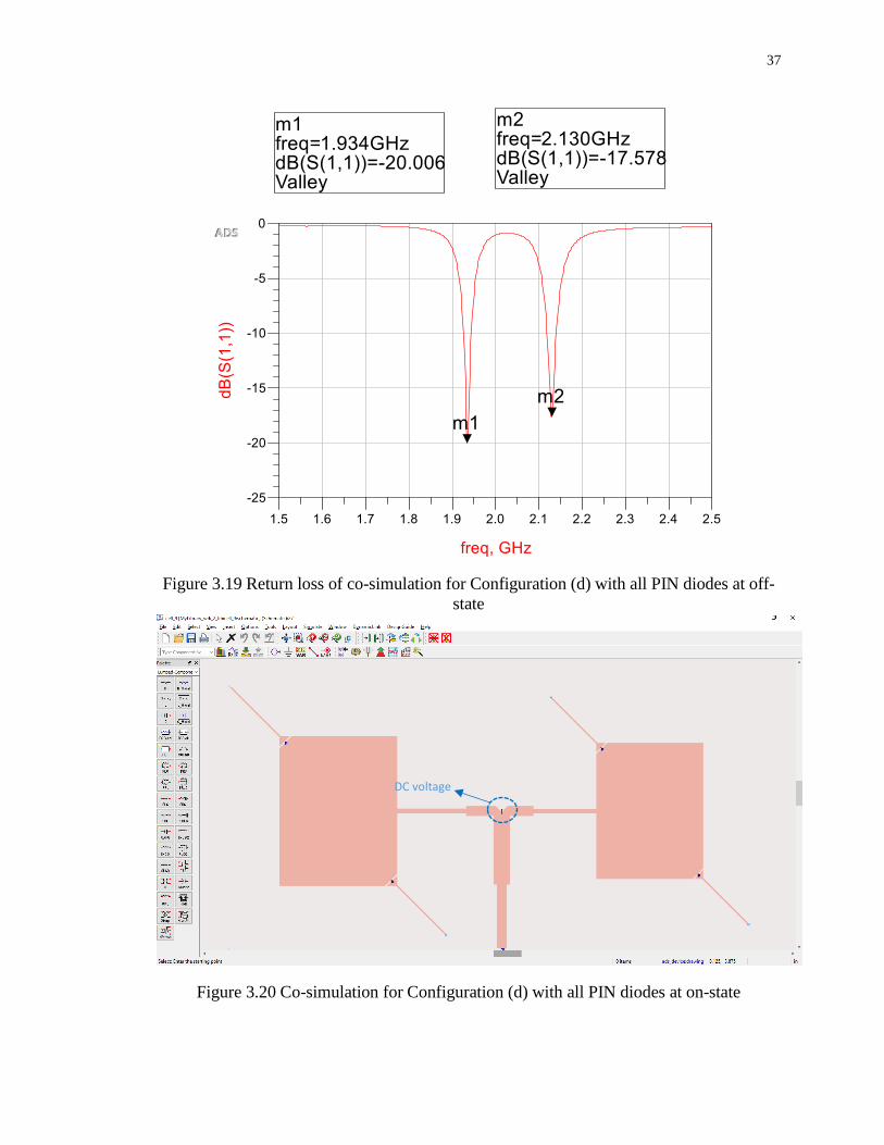
Figure 3.18: Co-simulation for configuration (d) with all pin-diodes at off-state………36
Figure 3.19: Return loss of Co-simulation for configuration (d) with all pin-diodes at off-
state………………………………………………………………………………….......37
Figure 3.20: Co-simulation for configuration (d) with all pin-diodes at on-state……....37
Figure 3.21: Detail of DC voltage………………………………………………..……..38
Figure 3.22: Return loss of Co-simulation for configuration (d) with all pin-diodes at on-
state……………………………………………………………………………………..38
Figure 3.23: Return loss for the antenna array when operating in different configurations
in simulation………………………………………………………………………….....40
Figure 3.24 (1) (2): The simulated radiation pattern of Configuration (a) and Configuration
(d)……………………………………………………………………………………......41
Figure 3.25: T tech mill machine used to fabricate proposed antenna array…………....43
Figure 3.26: Photograph of the proposed antenna array………………………………...44
Figure 3.27: Agilent network analyzer used to measure the proposed antenna array…..44

vi
Figure 3.28: Comparison of measured return losses of configuration (d) with and without
PIN
diodes……………………………………………………………………………….…....46
Figure 3.29: Return loss for the antenna array in different working Configurations between
simulation and measurement……………………………………………………...…......46
Figure 4.1: Geometry of Proposed Reconfigurable Yagi-Uda Patch Antenna…………..50
Figure 4.2: The geometry of a patch antenna with a switchable slot…………………….52
Figure 4.3 (a): Relative electric currents on the patch antennas at their resonant frequencies
with the switch OFF…………………………………………………………………......53
Figure 4.3 (b): Relative electric currents on the patch antennas at their resonant frequencies
with the switch ON…………………………………………………...........................….53
Figure 4.4: Layout design for the patch antenna with resonant frequency at 2.495GHz..54
Figure 4.5: Return loss of the proposed 2.495GHz single patch antenna……………….54
Figure 4.6: Basic antenna design with a slot………………………………………….....55
Figure 4.7: Return loss of a basic patch antenna with a slot…………………..…...........55
Figure 4.8: Basic antenna design with a metal piece in the center of slot……………....56
Figure 4.9: Return loss of a basic patch antenna with a metal piece in the center of slot.56
Figure 4.10: Basic patch antenna with parasitic elements…………………………...….58
Figure 4.11: Return loss of the antenna proposed in Figure 4.10……………...………. 59
Figure 4.12: Antenna proposed in Figure 4.8 with increased-size director elements…...59
Figure 4.13: Return loss of antenna proposed in Figure 4.10…………………………...60
Figure 4.14: Antenna proposed in Figure 4.8 with increased-size reflector elements…..61
Figure 4.15: Return loss of antenna proposed in Figure 4.12…………………...……....61

vii
Figure 4.16: Geometry of Proposed Reconfigurable Yagi-Uda Patch Antenna……........63
Figure 4.17: Layout simulation for proposed antenna with four metal pieces…………...64
Figure 4.18: Simulated return loss for proposed antenna with four metal pieces………..64
Figure 4.19: Layout simulation for proposed antenna without four metal pieces………..65
Figure 4.20: Simulated return loss for proposed antenna without four metal pieces….....66
Figure 4.21: Surface Current Distribution for Antenna Working at 2.41 GHz………......67
Figure 4.22: Surface Current Distribution for Antenna Working at 1.90 GHz………......67
Figure 4.23: Early design of the proposed 2.41 GHz antenna……………………………68
Figure 4.24: Return loss of early 2.41 GHz design………………………………………69
Figure 4.25: Pattern for the early 2.41 GHz design……………………………………....69
Figure 4.26: Early design of the proposed 1.90 GHz antenna……………………………70
Figure 4.27: Return loss of early 1.90 GHz design………………………………………70
Figure 4.28: Pattern for the early 1.90 GHz design………………………………………71
Figure 4.29: Radiation patterns of 2.41 GHz and 1.90 GHz for proposed antenna………72
Figure 4.30: Radiation intensity for two working frequencies…………………………...73
Figure 4.31: Stub connected to driven element by using metal piece at 2.41GHz ……....75
Figure 4.32: Stub disconnected to driven element at 1.90 GHz…….……………………75
Figure 4.33: Return loss for proposed antenna working at 2.41GHz …………………....76
Figure 4.34: Without two pieces of metal used to connect stubs and driven
element……………………………………………………………………..………….....76
Figure 4.35: Return loss for proposed antenna with 2 metal pieces that used to connect stubs
and driven pieces have been removed…………………………………………………....77
Figure 4.36: The T Tech mill machine used to build the proposed antenna………...…....78

viii
Figure 4.37: The T Tech mill machine controlled by a computer……………………...…79
Figure 4.38: Milling device of T Tech Mill Machine ……………………………………..79
Figure 4.39: Antenna layout structure in control software of mill machine……………....80
Figure 4.40: Antenna layout structure with a new added outline………………………….80
Figure 4.41: Prototype of the proposed 1.90GHz Yagi-Uda patch antenna………….…...81
Figure 4.42: Measurement of prototype 1.90GHz Yagi-Uda patch antenna (1).................82
Figure 4.43: Measurement of prototype 1.90GHz Yagi-Uda patch antenna (2)……….…82
Figure 4.44: Measurement result for 1.90GHzYagi-Uda patch antenna……….….....…...83
Figure 4.45: Prototype of the proposed 2.41GHz Yagi-Uda Patch Antenna……….…......83
Figure 4.46: Measurement of the prototype 2.41GHz Yagi-Uda patch antenna (1).…..….84
Figure 4.47: Measurement of the prototype 2.41GHz Yagi-Uda patch antenna (2).….…..84
Figure 4.48: Measurement result for 2.41 GHz Yagi-Uda patch antenna………….……..85
Figure 4.49: Simulation and Measurement results for proposed antenna without all four
metal pieces (Design working frequency is 1.90 GHz)………………………………..…86
Figure 4.50: Simulation and Measurement results for proposed antenna with all four metal
pieces (Design working frequency is 2.41 GHz)…………………………………………87
Figure 4.51: The layout structure for proposed antenna……………………………….…88
Figure 4.52: The proposed antenna with the metal piece loaded in the right slot has been
moved up 1mm……………………………………………………...…………………....88
Figure 4.53: The resonant point shift to 2.434 GHz based on the change has been made in
figure 4.52…………………………………………………………………….....……….89
Figure 4.54: The proposed antenna with the metal piece loaded in the right slot has been
moved down for 1mm…………………………………………………………….……...90

ix
Figure 4.55: The resonant point shift to 2.385 GHz based on the change has been made in
figure 4.54……………………………………...………………..…………………….…90
Figure 4.56: The proposed antenna with the height of metal pieces loaded in slots has been
increased by 0.2 mm………………………………………………….……………….…91
Figure 4.57: The resonant point shift to 2.424 GHz based on the change has been made in
figure 4.56………………………………………………………………………..……....91
Figure 4.58: The proposed antenna with the height of metal pieces loaded in slots has been
decreased by 0.2 mm…………………………………………………………………......92
Figure 4.59: The resonant point shift to 2.393 GHz based on the change has been made in
figure 4.58……………………………………………………….…………………….....92

1
Chapter 1. Introduction to Reconfigurable Patch Antennas
1.1 Introduction
Patch antennas are widely used today. They are used for satellite communications and
various military purposes such as GPS, mobile, missile systems, etc., due to their light
weight, simple structure and easy implementation. The main advantages of patch antennas
are as follows:
(1) Low cost to fabricate.
(2) Easy to manufacture.
(3) Efficient radiation.
(4) Support both linear and circular polarization.
(5) Light weight.
(6) Integrate easily with microwave integration circuits.
The increasing demand for modern mobile, satellite and wireless communication systems
have driven many researchers to work on improving performance and enhancing
applications of patch antennas. Reconfigurable antennas have drawn much attention for
future wireless communication systems due to their ability to modify their geometry to adapt
to changes in environmental conditions or system requirements such as enhanced
bandwidths, operating frequencies, polarizations, radiation patterns, etc. [1]. Microstrip
antenna is one of the most popular choices in designing the reconfigurable antenna because
of their advantages we introduced above. Reconfigurable antennas can be roughly classified
into three main types: reconfigurable frequency, reconfigurable polarization and
reconfigurable radiation pattern antennas. Usually, a reconfigurable antenna is realized by

2
using many kinds of RF switches, such as PIN diodes, Micro-electro-mechanical systems
(MEMs) and GaAs field-effect transistors (GaAs FETs).
A reconfigurable radiation pattern antenna reduces the effects of noisy environments by
changing the null positions, and it saves energy by adjusting the main beam signal towards
the intended user to improve the overall system performance. In [2], a single-feed switchable
feed network, which replaces the traditional PIN diode or MEM, was used to obtain pattern
diversity. In [3], a wide-band L-probe circular patch antenna was presented with dual feeds
and an integrated matching network with switches. In order to reconfigure the radiation
pattern electrically, the structure of this matching system is relatively complex. In [4], the
method of switching load to reconfigure the pattern of antenna is used. A MEMs-switched
parasitic antenna array providing radiation pattern diversity with a novel modeling method
was proposed in [5]. A novel equilateral triangular patch antenna with two diverse patterns
working at nearly the same resonant frequency was proposed in [6]. In [7], a pattern
reconfigurable antenna based on a two-element dipole array model with a new structure is
introduced by this author. In [8], they explored a very compact planar radiation pattern
reconfigurable antenna using metasurface. In [9], they proposed a compact, low-profile,
high impedance surface (HIS)-based, pattern reconfigurable antenna generating a broad
and tilted beam. In [10], a new method to reconfigure the radiation pattern of a simple
circular patch antenna with shorting pins located at the edge of the patch was presented.
Genetic Algorithm (GA) and Finite Element software was used to simulate and optimize
the impact of the shorting pins on this antenna.
Compared to traditional broadband antennas, frequency reconfigurable antennas have a
relatively smaller size and higher isolation [11]. In [12], a frequency reconfigurable patch

3
was proposed that used 19 reed switches, which replace bias and control circuits, to connect
the patch with the ground plane. [13] was introduced a compact frequency-reconfigurable
patch antenna capable of switching between three operating bands, with the feature of
shorting load. In [14] frequency agility was achieved by integrating a varactor diode
between the patch and the ground to make a frequency reconfigurable antenna. This
method also reduced the antenna size. Presented in [15] was a frequency reconfigurable
microstrip patch antenna using Defected Ground Structure (DGS) with aperture coupled
feed line. In [16], a multilayer frequency reconfigurable patch antenna for high frequency
was proposed. In [17], a novel frequency-reconfigurable antenna based on a circular
monopole patch antenna was presented. The proposed antenna consists of a center-fed
circular patch and four sector-shaped patches surrounding it. By controlling eight varactor
diodes, which are introduced to bridge the gaps between the circular patch and the sector-
shaped patches, different working frequencies can be achieved. A novel design of
frequency-reconfigurable antenna by using an aperture-coupled feeding technique and
stacked patch structure was introduced [18]. An octagonal-shaped frequency
reconfigurable patch antenna was designed and studied in [19]. In this antenna design, open
ended L-slots have been used on both sides of the patch and four PIN diodes are used for
the operation of this antenna. In [20] is a design for a frequency reconfigurable antenna
with conical-beam radiation. The design is based on a coplanar annular-ring microstrip
antenna that works on the 𝑇𝑀02 mode, and several shorting strips that are symmetrically
placed along the circumference of the radiating patch and are used to vary its resonant
frequency.

4
Polarization reconfigurable antennas have drawn increasing attention because they have
some desirable advantages for modern wireless communications, such as avoiding fading
loss caused by multipath effects in wireless local area networks, providing a powerful
modulation scheme in active read/write microwave tagging systems, realizing frequency
reuse to expand the capability in satellite communication systems, and being a suitable
candidate in multiple-input-multiple-output (MIMO) systems [21]. The study in [22]
proposed a polarization reconfigurable patch antenna with polarization states that can be
switched among linear polarization (LP), left-hand (LH) and right hand (RH) circular
polarizations(CPs). The CP waves of this antenna are caused by two perturbation elements
of loop slots in the ground plane. In [23], a new polarization reconfigurable-agile antenna,
which is based on a quad-mode reconfigurable feeding network with four dynamic
transmission modes, was proposed. This antenna can be switched between four different
polarizations. [24] introduced a new quadri-polarization reconfigurable circular patch
antenna which is composed of a circular radiating patch and a switchable feed network. A
stub-loaded microstrip patch antenna with both frequency and polarization selectivity was
proposed in [25].
We will focus on pattern and frequency reconfigurable antennas in this thesis. There is
a developmental trend in wireless communication systems that requires the use of antennas
capable of accessing services in various frequency bands, sometimes with the use of a
single antenna. So far, most of the reported pattern reconfigurable antennas can only switch
the beam in a limited range. And there are few antenna designs concerned with both
radiation pattern and dual-frequency. A pattern reconfigurable antenna that has multiband
characteristics improves the whole system performance.
5
1.2 Objectives
The objective of this thesis is to design, fabrication and testing of two different
reconfigurable patch antennas.
The first antenna proposed in this thesis is a novel dual-frequency antenna array with
multiple pattern diversities. The desired resonant frequencies of two microstrip patch
antenna elements are 1.92 GHz and 2.11 GHz, respectively. These frequencies can be used
in wideband code division multiple access (WCDMA) communication systems. According
to [2], a single-feed switchable feed network can be used as a basic beam pattern
reconfigurable antenna system, and it also introduced dual-frequency features of the
antenna system. We use the structure demonstrated in [26] to create more pattern selectivity
and investigate the impact of this structure on the pattern of the antenna array. This array
antenna has been constructed on a RO4350B substrate with 1.52-mm thickness that has a
dielectric constant of 3.48 and size 208mm ×135mm.
The second antenna proposed in this thesis is a pattern and frequency reconfigurable
Yagi-Uda patch antenna. The proposed working frequencies for this antenna are 1.90 GHz
and 2.41 GHz. which are suitable for LTE and Wi-Fi networks, respectively. The proposed
Yagi-Uda patch antenna consists of two reflectors, a driven element and six director
elements. The reflector elements and director elements are tuned properly in frequency
compared to the driven element when using ADS. Two slots were used in the driven
element to introduce frequency and pattern reconfigurabilities to this antenna system. Two
stubs, which were used to improve the return loss performance and adjust working
frequency, were connected to the driven element when working in the 2.41GHz mode. Four
metal pieces were used to imitate PIN-diodes in simulation and measurement. In order to

6
validate the effectiveness of our design, we built two antennas – one with and one without
these metal pieces (2.41GHz mode and 1.90 GHz mode, respectively). The two antennas
with different modes were fabricated on RO4350B substrate with 1.52-mm thickness. The
measured and simulated results agree very well.
The proposed antennas were simulated using Advanced Design System [ADS], and
fabricated using a new model of a T Tech Mill machine. Aglient network Analyzer is used
to measure the return losses of proposed antennas.
1.3 Outline of the Thesis
This thesis consists of five chapters. The overview of each chapter follows.
Chapter 1: Provides the introduction, motivation and objective of this master thesis and
includes the literature review on reconfigurable patch antennas.
Chapter 2: Presents the fundamentals of Microstrip Patch Antennas (MSAs), including
the fundamental geometries and characteristics of the MSA, feeding technology, and the
methods of analysis used for the MSA design.
Chapter 3: Presents the design, fabrication and testing of a novel dual-frequency patch
array antenna with multiple pattern reconfigurabilities. The beam pattern selectivity can be
obtained by utilizing a switchable feeding network and the special structure used in this
array antenna. There are two opposite corners which have been slotted on each patch and
a diode on the slot which is used as a switch to control multiple patterns. By controlling
four PIN diodes through the corresponding DC voltage source, the radiation pattern can be
changed. The simulation and measurement results agree nearly with each other.
Chapter 4: Presents the design, fabrication and testing of a novel pattern and frequency
reconfigurable Yagi-Uda patch antenna. This Yagi-Uda patch antenna consists of two

7
reflectors, a driven element and six director elements. The reflector elements and director
elements are tuned properly in frequency compared to the driven element. Two slots were
used in the driven element to introduce frequency and pattern selectivity to this antenna
system. Two stubs have been connected to the driven element when it’s working in 2.41
GHz so as to improve the returnloss performance and adjust working frequency. The
simulated and measured return loss results agree nearly with each other.
Chapter 5: Presents the conclusions of this thesis.
Chapter 2. Theory of Microstrip Patch Antenna
2.1 Introduction
Low profile antennas have drawn much attention because they are suitable for high-
performance aircraft, spacecraft and satellite and missile applications, where size, weight,
cost, performance, ease of installation, and aerodynamic profile are significant constraints.
For today’s rapidly-developing mobile or personal communication devices, there exists
same need for compact and low profile antennas. Microstrip antennas (also referred to as
patch antennas or microstrip patch antennas) can be used in a wide range of applications
from commercial communication systems to satellites, and even biomedical applications
[27]. Chapter 14 of Antenna Theory: Analysis and Design [27] contributes greatly to the
fundamentals of patch antenna addressed in this chapter of the thesis.
2.2 Basic Characteristics of a Microstrip Patch Antenna
The history of patch antenna can be traced back to 1953, when G.A. Deschamps first
proposed this kind of antenna. However, patch antennas didn't become practical until the

8
1970s. In that time, it was developed further by researchers such as Robert E. Munson and
others by using low-loss soft substrate materials that were just becoming available during
that time.
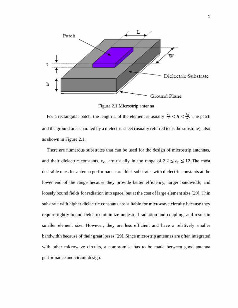
Based on [27], a microstrip antenna (Patch antenna), as shown in Figure 2.1, normally
consists of a very thin (t<<𝜆0 where 𝜆0 is the free-space wavelength) metallic patch placed
a small fraction of a wavelength (h<<𝜆0, usually 0.003𝜆0 ≤ ℎ ≤ 0.05𝜆0) above a ground
plane. The distance between the patch and the ground plane – the substrate or dielectric
height h – determines the bandwidth of antenna. A relatively thicker substrate can increase
the gain, but it may result in some undesired effects such as surface wave excitation.
Surface waves can decrease efficiency and perturb the radiation pattern. The patch antenna
is designed so its pattern maximum is normal to the patch (broadside radiator). This is
accomplished by properly choosing the mode (field configuration) of excitation beneath
the patch. In general, modes are designated as TMnmp. The ‘p’ value is mostly omitted
because the electric field variation is considered negligible in the z-axis since only a phase
variation exists in the z axis. So, TMnm represents the field variations in the x and y
directions. The field variation in the y direction (impedance width direction) is negligible
and so m is considered 0. The field has one minimum-to-maximum variation in the x
direction (resonance length direction and a half-wave long), thus n is 1 in this case, and we
say that this patch operates in the TM10 mode [28].
9
Figure 2.1 Microstrip antenna
For a rectangular patch, the length L of the element is usually 𝜆0
3< ℎ <
𝜆0
2. The patch
and the ground are separated by a dielectric sheet (usually referred to as the substrate), also
as shown in Figure 2.1.
There are numerous substrates that can be used for the design of microstrip antennas,
and their dielectric constants, 𝜀𝑟 , are usually in the range of 2.2 ≤ 𝜀𝑟 ≤ 12 .The most
desirable ones for antenna performance are thick substrates with dielectric constants at the
lower end of the range because they provide better efficiency, larger bandwidth, and
loosely bound fields for radiation into space, but at the cost of large element size [29]. Thin
substrate with higher dielectric constants are suitable for microwave circuity because they
require tightly bound fields to minimize undesired radiation and coupling, and result in
smaller element size. However, they are less efficient and have a relatively smaller
bandwidth because of their great losses [29]. Since microstrip antennas are often integrated
with other microwave circuits, a compromise has to be made between good antenna
performance and circuit design.

10
Basically, microstrip antennas are also referred to as patch antenna. Usually, the
radiating elements and feed lines of micorstrip antennas are photoetched on the dielectric
substrate. The radiating patch is generally made of conducting material such as copper or
gold and can be any possible shape, such as rectangular, thin strip (dipole), circular,
elliptical, triangular, etc. These and others are illustrated in Figure 2.2. Among the possible
shapes, the square, rectangular, dipole, and circular are the most common because they are
easy to analyze and fabricate. As well, they have other attractive characteristics, especially
low cross-polarization radiation. Microstrip dipoles are attractive because they inherently
possess a larger bandwidth and occupy less space, which makes them very suitable for
arrays [30], [31], [32], [33]. Linear and circular polarization patch antennas can be obtained
with either single elements or arrays of microstrip antennas. An array of microstrip
elements, with single or multiple feeds, can also be used to introduce scanning capabilities
and achieve greater directivities.
Figure 2.2 Different shapes of patch antenna

11
2.2.1 Radiation Pattern of a Patch Antenna
A patch antenna radiates energy in certain directions and we say that the antenna has
directivity (usually expressed in dBi). So far, the directivity usually has been defined
relative to an isotropic radiator. An isotropic radiator emits an equal amount of power in
all directions and it has no directivity. If the antenna has a 100% radiation efficiency
(meaning the energy delivered to the antenna can be 100% radiated from antenna), all
directivity would be converted to gain. The typical rectangular patch excited in its
fundamental mode has a maximum directivity in the direction perpendicular to the patch
(z-axis). The directivity decreases when moving away from zenith direction towards lower
elevations. Figure 2.3 shows a typical radiation pattern for half-wave square patch antenna
[28].
Figure 2.3 Radiation pattern for half-wave square patch antenna [28]

12
2.2.2 Polarization of a Patch Antenna
The plane in which the electric field varies is also known as the polarization plane. The
basic patch antenna is linearly polarized since the electric field varies in only one direction.
However, a large number of applications such as satellite communications, do not work
well with linear polarization because, due to the moving antenna platform, the relative
orientation of the antenna is unknown. In these applications, circular polarization is useful
since it is not sensitive to antenna orientation. Basic antennas do not generate circular
polarization; hence some changes have to be made to the patch antenna to enable it to
generate circular polarization. For a circularly polarized patch antenna, the electric field
varies in two orthogonal planes (x and y directions) with the same magnitude but a 90°
phase difference, as shown in Figure 2.4. Necessary to generate circular polarization for a
patch antenna is the simultaneous excitation of two modes, i.e. the TM10 mode (x direction)
and the TM01 mode (y direction). One of the modes is excited with a 90° phase delay to
the other mode. A circularly polarized antenna can either be right-hand circular polarized
(RHCP) or left-hand circular polarized (LHCP). The antenna is RHCP when the phases are
0° and -90° for the antenna in Figure 2.4, and the signal radiates towards the reader. It is
LHCP when the phases are 0° and +90°, and the signal radiates away [28].

13
Figure 2.4 The nearly square antenna for circular polarization [28]
2.2.3 Bandwidth of a Patch Antenna
The impedance bandwidth depends on a large number of parameters related to the patch
antenna element itself like quality factor, Q, and the type of feed technology used. Usually,
the impedance bandwidth of a square, half-wave patch antenna is typically limited to 1 to
3%, which is a major disadvantage of this type of patch antenna. [28]
2.3 Feeding Method
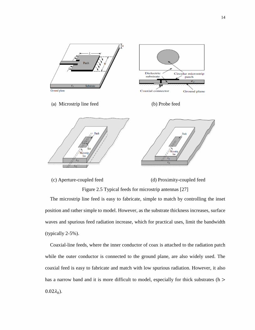
There are many configurations that can be used to feed microstrip antennas. The four
most popular are the microstrip line, coaxial probe, aperture coupling and proximity
coupling [27]. These are all displayed in Figure 2.5.
14
(a) Microstrip line feed (b) Probe feed
(c) Aperture-coupled feed (d) Proximity-coupled feed
Figure 2.5 Typical feeds for microstrip antennas [27]
The microstrip line feed is easy to fabricate, simple to match by controlling the inset
position and rather simple to model. However, as the substrate thickness increases, surface
waves and spurious feed radiation increase, which for practical uses, limit the bandwidth
(typically 2-5%).
Coaxial-line feeds, where the inner conductor of coax is attached to the radiation patch
while the outer conductor is connected to the ground plane, are also widely used. The
coaxial feed is easy to fabricate and match with low spurious radiation. However, it also
has a narrow band and it is more difficult to model, especially for thick substrates (h >
0.02𝜆0).

15
Both the microstrip feed line and the probe possess inherent asymmetries which generate
higher order modes which produce cross-polarized radiation. Non-contacting aperture
coupling feeds, as shown in Figures 2.5 (c) and (d), have been introduced to overcome
some of these problems mentioned above. For a basic aperture coupled patch antenna,
shown in Figure 2.5 (c), the radiating microstrip patch element is etched on the top of the
antenna substrate, and the microstrip feed line is etched on the bottom of the feed substrate.
The thickness and dielectric constants of these two substrates may thus be chosen
independently to optimize the distinct electrical functions of radiation and circuitry.
Although the original prototype antenna used a circular coupling aperture, it was quickly
realized that the use of a rectangular slot would improve the coupling, for a given aperture
area, due to its increased magnetic polarizability. Most aperture coupled microstrip
antennas now use rectangular slots, or variations thereof. Proximity coupling, shown in
Figure 2.5 (d), has the largest bandwidth among these four feeding methods, and has low
spurious radiation. However, fabrication is difficult. Length of feeding stub and width-to-
length ratio of patch can be used to control the match performance.
In general, the input feed point for the antenna must be placed in such a point along the
transmission line where the input impedance match is 50 Ω, and the antenna reactance must
be minimized as much as possible.
2.4 Method of Analysis
There are many methods of analysis for microstrip antenna. Comparing to other
methods, the transmission line method is the easiest method. It gives good physical
insight, representing the rectangular patch as a pair of two radiating slots, separated by a

16
low-impedance (𝑍𝑐) transmission line of certain length L. However, this method is less
accurate and it is more difficult to model coupling [27].
2.4.1 Fringing Effects
Because the dimensions of the patch are finite along the length and width, the fields at
the edges of the patch undergo fringing. It is the fringing fields that are responsible for the
radiation. This is illustrated along the length in Figure 2.6 for the two radiating slots of the
microstrip antenna. The amount of fringing is a function of the dimensions of the patch and
the height of the substrate. For the principal E-plane, fringing is a function of the ratio of
the length of the patch L to the height h of the substrate (L/h) and the dielectric constant 𝜀𝑟
of the substrate. Since for microstrip antennas L/h >> 1, fringing is reduced. However, it
must be taken into account because it influences the resonant frequency of the antenna.
Because of the fringing effect, in which some of the waves travel in the substrate and some
in air, an effective dielectric constant 𝜀𝑟𝑒𝑓𝑓 is introduced to account for this effect.
Figure 2.6 Microstrip antenna and its electric filed lines

17
The effective dielectric constant is defined as the dielectric constant of the uniform
dielectric material so that the electric field lines have identical electrical characteristics,
particularly the propagation constant, as the actual field line.
The value of the effective dielectric constant is essentially constant at low frequencies,
then increasing monotonically as the frequency increases, and ends up approaching the
value of the dielectric constant of the substrate at higher frequencies. The initial values (at
low frequencies) of the effective dielectric constant are referred to as the static values, and
they are given by [34]:
W/h>1
𝜀𝑟𝑒𝑓𝑓 =𝜀𝑟+1
2+
𝜀𝑟−1
2[1 + 12
ℎ
𝑊]−
1
2 (2-1)
Where 𝜀𝑟𝑒𝑓𝑓 = Effective dielectric constant
𝜀𝑟 = Dielectric constant of substrate
h = Height of dielectric substrate
W=Width of the Patch
2.4.2 Effective Length and Resonant Frequency
In the transmission line model, the antenna is represented by two radiating slots (W×h)
separated by a low impedance transmission line (𝑍𝑐) of length L. The slots represent very
high-impedance terminations from both sides of the transmission line (almost an open
circuit). Thus, we expect this structure to have highly resonant characteristics depending
mainly on its length L. Due to the fringing effect, the resonant length of the patch is not
exactly equal to the physical length. The fringing effect makes the physical length of

18
antenna shorter than the effective electrical length of the patch. The dimensions of the patch
along its length have been elongated on each end by a length of ∆L, which is a function of
the effective dielectric constant 𝜀𝑟𝑒𝑓𝑓 and the width-to-height ratio (W/h). A well-known
and practical approximate relation for the normalized extension of the length show as
follows:
𝐿𝑒𝑓𝑓 = 𝐿 + 2Δ𝐿 (2-2)
𝐿𝑒𝑓𝑓 =1
2𝑓𝑟√𝜇0𝜀0√𝜀𝑟𝑒𝑓𝑓=
𝑣0
2𝑓𝑟√𝜀𝑟𝑒𝑓𝑓 (2-3)
ΔL = 0.412h(𝜀𝑟𝑒𝑓𝑓+0.3)(
𝑊
ℎ+0.264)
(𝜀𝑟𝑒𝑓𝑓−0.258)(𝑊
ℎ+0.8)
[35] (2-4)
For dominant 𝑇𝑀010 mode 𝑓𝑟 is:
𝑓𝑟010 =1
2𝐿√𝜇0𝜀0√𝜀𝑟=
𝑣0
2𝐿√𝜀𝑟 (2-5)
Where 𝑣0 is the speed of light in free space. The resonant frequency of a patch depends
highly on L. Because (2-5) does not account for fringing, it must be modified to include
edge effects and when the fringing effect is taken into account, (2-5) becomes
𝑓𝑟010 =1
2𝐿𝑒𝑓𝑓√𝜇0𝜀0√𝜀𝑟𝑒𝑓𝑓=
1
2(𝐿+2ΔL)√𝜇0𝜀0√𝜀𝑟𝑒𝑓𝑓 (2-6)
=q1
2𝐿√𝜇0𝜀0√𝜀𝑟= 𝑞
𝑣0
2𝐿√𝜀𝑟
Where q =𝑓𝑟𝑐010
𝑓𝑟010 (2-6a)
The q factor is referred to as the fringe factor (length reduction factor). As the substrate
height increases, fringing also increases and results in larger separations between the
radiating edges and lower resonant frequencies.

19
Figure 2.7 Physical and effective lengths of rectangular microstrip patch antenna
2.4.3 Effective Width
For an effective radiator, a practical width that leads to good radiation efficiencies is:
W =1
2𝑓𝑟√𝜇0𝜀0√
2
𝜀𝑟+1=
𝑣0
2𝑓𝑟√
2
𝜀𝑟+1 (2-7)
Where 𝑣0 is the free-space velocity of light [36].
The procedure of designing a rectangular patch using the transmission line model is as
follows:
(1) Input data: 𝜀𝑟, 𝑓𝑟 (𝑖𝑛 𝐻𝑧), and h
(2) Calculate W using (2-7),
W =1
2𝑓𝑟√𝜇0𝜀0
√2
𝜀𝑟 + 1=
𝑣0
2𝑓𝑟
√2
𝜀𝑟 + 1
(3) Calculate 𝜀𝑟𝑒𝑓𝑓 using (2-1),
𝜀𝑟𝑒𝑓𝑓 =𝜀𝑟 + 1
2+
𝜀𝑟 − 1
2[1 + 12
ℎ
𝑊]−
12
(4) Calculate the actual (physical) length of the patch using (2-2), (2-3) and (2-4)

20
L =1
2𝑓𝑟√𝜇0𝜀0√𝜀𝑟𝑒𝑓𝑓-2ΔL
= 𝑣0
2𝑓𝑟√𝜀𝑟𝑒𝑓𝑓− 2ΔL

21
Chapter 3. A Proposed Novel Dual-Frequency Array Antenna
with Multiple Pattern Reconfigurabilities
3.1 Introduction
This chapter presents the design, fabrication and testing of a novel dual-frequency array
antenna with multiple pattern reconfigurabilities. The transmission line model is
implemented to calculate the basic dimensions of the conventional MSA. The Advanced
Design System [ADS] software is used in modeling and simulating the designed antennas.
The beam pattern selectivity can be obtained by utilizing a switchable feeding network and
the special structure used in this array antenna. Opposite corners have been slotted on each
patch and a diode placed on the slot, which is used as a switch to control multiple patterns.
By controlling four PIN diodes through the corresponding DC voltage source, the radiation
pattern can be changed. The simulation and measurement results closely agree.
3.2 Basic single patch antenna design
In this section, a novel dual-frequency antenna array with multiple pattern diversities is
proposed. The desired resonant frequencies of two microstrip patch antennas are 1.92 GHz
and 2.11 GHz, respectively. The proposed antenna array consists of two different patch
antenna elements. The first step of designing the proposed antenna array is designing its two
patch antenna elements.
To design two conventional rectangular patch antenna elements with operating
frequencies of 1.92GHz and 2.11GHz respectively, we should follow the method discussed
in chapter 2. The width of patch antenna elements can be found using (2-7):
𝑊1.92 =1
2𝑓𝑟1.92√𝜇0𝜀0√
2
𝜀𝑟+1=
𝑣0
2𝑓𝑟1.92√
2
𝜀𝑟+1 (3-1)

22
=3×10⁸
2×1.92×109√
2
1+3.6
=51.5mm
𝑊2.11 =1
2𝑓𝑟2.11√𝜇0𝜀0√
2
𝜀𝑟+1=
𝑣0
2𝑓𝑟2.11√
2
𝜀𝑟+1 (3-2)
=3×10⁸
2×2.11×109√
2
1+3.6
=46.8mm
To find the effective dielectric constant, 𝜀𝑟𝑒𝑓𝑓, and when W/h >1 , we can use (2-1):
𝜀𝑟𝑒𝑓𝑓1.92 =𝜀𝑟+1
2+
𝜀𝑟−1
2[1 + 12
ℎ
𝑊1.92]−
1
2 (3-3)
=3.6+1
2+
3.6−1
2[1 + 12
1.524
51.5]−
1
2
=2.3+1.3[1 + 0.355]−1
2
=3.421
𝜀𝑟𝑒𝑓𝑓2.11 =𝜀𝑟+1
2+
𝜀𝑟−1
2[1 + 12
ℎ
𝑊2.11]−
1
2 (3-4)
=3.6+1
2+
3.6−1
2[1 + 12
1.524
46.8]−
1
2
=2.3+1.3[1 + 0.399]−1
2
=3.399
This value for 𝜀𝑟𝑒𝑓𝑓 is reasonable, because 1 ≤ 𝜀𝑟𝑒𝑓𝑓≤𝜀𝑟.
The effective length can be found using (2-2), (2-3) and (2-4):
𝐿𝑒𝑓𝑓1.92 =𝑐
2𝑓1.92√𝜀𝑟𝑒𝑓𝑓1.92 (3-5)
=3×10⁸
2×1.92×109√3.421
=3
38.4×1.85

23
=3
71.04
=42.2mm
𝐿𝑒𝑓𝑓2.11 =𝑐
2𝑓2.11√𝜀𝑟𝑒𝑓𝑓2.11 (3-6)
=3×10⁸
2×2.11×109√3.399
=3
42.2×1.845
=3
77.859
=38.5mm
Δ𝐿1.92 = 0.412h(𝜀𝑟𝑒𝑓𝑓1.92+0.3)(
𝑊1.92ℎ
+0.264)
(𝜀𝑟𝑒𝑓𝑓1.92−0.258)(𝑊1.92
ℎ+0.8)
(3-7)
=0.412×1.524×10−3×(3.421+0.3)(
51.5
1.524+0.264)
(3.421−0.258)(51.5
1.524+0.8)
=(3.721)(33.79+0.264)
(3.163)(33.79+0.8)×0.628×10−3
=126.71
109.41×0.628×10−3
=0.00073m
=0.73mm
𝐿1.92 = 𝐿𝑒𝑓𝑓1.92 − 2Δ𝐿1.92
=42.2-1.46
=40.74mm
Δ𝐿2.11 = 0.412h(𝜀𝑟𝑒𝑓𝑓2.11+0.3)(
𝑊2.11ℎ
+0.264)
(𝜀𝑟𝑒𝑓𝑓2.11−0.258)(𝑊2.11
ℎ+0.8)
(3-8)
=0.412×1.524×10−3×(3.399+0.3)(
46.8
1.524+0.264)
(3.399−0.258)(46.8
1.524+0.8)

24
=(3.699)(30.71+0.264)
(3.141)(30.71+0.8)×0.628×10−3
=114.57
98.97×0.628×10−3
=0.000727m
=0.727mm
𝐿2.11 = 𝐿𝑒𝑓𝑓2.11 − 2Δ𝐿2.11
=38.5-1.454
=37.05mm
We used the side line feeding method, with the width of the feeding line being
determined by ADS simulation.
Figure 3.1 Layout simulation for Basic Antennas
Figure 3.1 shows the layout simulation for two basic antennas. Many simulation and
optimization works based on the basic parameters were developed from the equations.
After the optimization works, the dimensions of two antenna elements were set to 51.8 mm
× 40.72 mm (1.92GHz) and 47.12 mm × 36.98 mm (2.11 GHz), respectively. In the future
work, we will design our desired antenna array based on these two basic elements.

25
(a)
(b)
Figure 3.2 Return loss for two basic antenna elements
Based on Figure 3.2 we can conclude that these two patch antenna worked well at the
expected frequencies.

26
3.3 Dual-frequency pattern reconfigurable antenna array design
In this section, the design of the dual-frequency pattern reconfigurable array antenna
based on those two antenna elements from Section 3.2 above is discussed. According to [2],
a single-feed switchable feed network can be used as a basic beam pattern reconfigurable
antenna system that also introduces dual-frequency features to the antenna system. We use
the structure discussed in [26] to create more pattern selectivity and investigate the impact
of this structure to the pattern of the antenna array.
3.3.1 Switchable feeding network
The two antenna elements were connected by a single-feed switchable network. The
basic schematic of the single-feed switchable feed network is shown in Figure 3.3.
According to [2], the principle of operation of this switchable feed network is based on the
assumption that the resonant frequency ratio of the two micro-strip patch antennas is very
close to 1.4:1. It basically consists of two quarter-wavelength branch lines with
characteristic impedances of Z1 and Z2 and lengths of L1 and L2 . Two different
rectangular micro-strip patch antennas of different size were connected to output ports 2
and 3. Under this particular condition, the single-feed switchable feed network can be
worked as an ideal switch.
Figure 3.3 Schematic of a single-feed switchable feed network.
INPUT
OUTPUT
OUTPUT
𝑍1
𝑍2
𝐿1
𝐿2
PORT1
PORT2
PORT3

27
3.3.2 Antenna array design
The schematic structure of the proposed antenna array is shown in Figure 3.4, along with
all sizes and dimensions listed in Table 3.1. Two rectangular patches are used as the basic
radiating elements. The patches have dimensions of 51.8 mm × 40.72 mm (1.92GHz) and
47.12 mm × 36.98 mm (2.11 GHz), respectively. The PIN diodes, which are loaded in the
gaps between antenna and truncated corners, can be controlled by DC voltage through the
short lines of quarter waveguide length and via holes. The quarter-wavelength lines at each
of the truncated corners combined with the isolation area can also be used to mitigate the
influences of direct current on the microwave signal and to block the RF energy to DC
sources [26]. The gaps between patch antennas and truncated corners are set to be 0.51mm.
Infineon BAR63-03W diodes, of size 2.5mm × 1.25mm, are used as RF switches.
Figure 3.4 Geometry of built array antenna
TABLE 3.1 PARAMETER VALUES OF THE PROPOSED ANTENNA
W1 51.8mm W2 47.12mm W3 0.495mm W4 0.495mm W5 1.7 mm
W6 3.48mm W7 1.5mm W8 5.67mm W9 3.38mm L1 40.72mm
L2 36.98mm L3 24.06mm L4 22.10mm L5 23.33mm L6 21.78mm
L7 23.81mm S1 4.71mm S2 5.06mm L8 23.72mm R 0.5mm
L1 L2
W1 W2
R
W3
W5 W6 W7
W8
W9
L3 L4
L6 L8
Pin Diode
SW1 SW2 Patch 1 Patch 2
L7 L5
SMA Connector
W4
Via Hole

28
The diode used is equivalent to a resistor of 1.2 Ω when it is forward-biased and to a
capacitor of 0.21pF when it is reverse-biased. The optimized geometrical parameters are
shown in Table 1. Two rectangular patch antennas of different sizes are connected to the
corresponding outputs of the switchable feed network.
The following figures (3.5) – (3.8) are four different simulated designs of this array
antenna that were developed using Advance Design System (ADS) software in order to
determine how the truncated corners impact the performance of the antenna array.
Configuration (a) is the basic antenna array with short lines of quarter waveguide length,
shown in Figure 3.5; Configuration (b) is the antenna array with short lines of quarter
waveguide length and truncated corners on the 1.92GHz antenna element, shown in Figure
3.6; Configuration (c) shows the antenna array with short lines of quarter waveguide length
and truncated corners on the 2.11GHz antenna element, shown in Figure 3.7 and;
Configuration (d) shows the antenna array with short lines of quarter waveguide length and
truncated corners on both antenna elements, shown in Figure 3.8. To easily validate the
effectiveness of our design, we built and measured Configuration (d). However, by
incorporating four PIN-diodes and a DC voltage into Configuration (d), we can investigate
properties between different configurations such as (a) (Figure 3.5) and (d) (Figure 3.8.).

29
.
Figure 3.5 Configuration (a): Basic antenna array with short lines of quarter waveguide length
Figure 3.6 Configuration (b): Antenna array with short lines of quarter waveguide length and truncated
corners on the 1.92GHz antenna element
Switchable Feed Network
Slotted corner

30
Figure 3.7 Configuration (c): Antenna array with short lines of quarter waveguide length and truncated
corners on the 2.11GHz antenna element
Figure 3.8 Configuration (d): Antenna array with short wires of quarter waveguide length and truncated
corners on both antenna elements
Slotted corner
Slotted corner
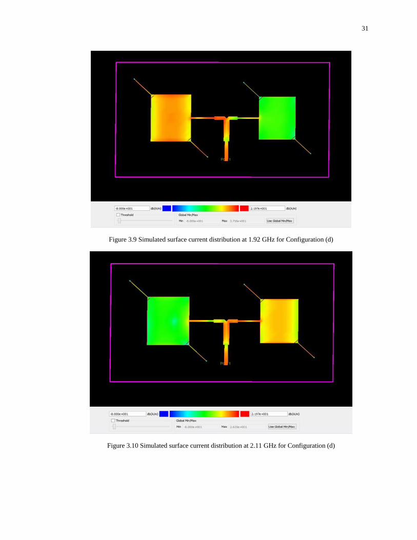
31
Figure 3.9 Simulated surface current distribution at 1.92 GHz for Configuration (d)
Figure 3.10 Simulated surface current distribution at 2.11 GHz for Configuration (d)

32
Figure 3.9 and Figure 3.10 show the simulated surface current distribution around the
designed resonant frequency, proving the effectiveness of the switchable network used in
the antenna syatem.
Figure 3.11 Axial Ratio for antenna array of configuration (d) at working
frequency of 1.92 GHz (left) and 2.11 GHz (right)
As can be seen from Figure 3.11, the axial ratio of this antenna array at each working
center frequency of Configuration (d) in the main lobe direction are all greater than 10 dB.
This means the antenna array of Configuration (d) works in linear polarization mode for
two different working frequencies.
Figure 3.12 Return loss for configuration (d)

33
Figure 3.12 shows the return loss performance is very good at two working frequencies
after many simulation and optimization works have been done. After the Configuration (d)
had been built, we added four PIN diodes and a DC voltage into the antenna system. These
changes have impacts on the antenna system. In order to determine the impact on antenna
return loss performance, we used the co-simulation function of ADS. Figure 3.13-3.22 show
how to use the co-simulation function and the return loss performance for co-simulation
work.
Figure 3.13 Configuration (d) with additional ports
To begin to do co-simulation, many ports need to be added into the design, shown in
Figure 3.13. The detail of two ports can be observed in Figure 3.14. These ports are the
positions where PIN diodes and DC voltage will be brought into the schematic simulation.
After all the ports were added to the system, a new simulation can be run.
Next, an EM model needs to be created by selecting EM > Component > Create EM
Model and Symbol in the layout window, shown in Figure 3.15.

34
Finally, the newly created EM model is introduced to a new schematic simulation, shown
in Figure 3.16. Then many schematic items, such as PIN diodes, DC voltage, wire and S-
parameter simulation control, were added into the antenna system. Figure 3.17 shows a PIN
diode that has been added into the antenna system to control the pattern of the proposed
antenna.
Figure 3.14 Detail of two additional added ports

35
Figure 3.15 Creating a new EM Model
Figure 3.16 Introducing new EM Model to schematic design

36
Figure 3.17 A PIN diode that has been added to the schematic simulation
Figure 3.18 Co-simulation for Configuration (d) with all PIN diodes at off-state
37
Figure 3.19 Return loss of co-simulation for Configuration (d) with all PIN diodes at off-
state
Figure 3.20 Co-simulation for Configuration (d) with all PIN diodes at on-state
DC voltage

38
Figure 3.21 Detail of the DC voltage
The forward voltage of our PIN diode is 1.2 V, thus a 1.5 V DC-voltage is sufficient to
control the PIN diodes.
Figure 3.22 Return loss of co-simulation for Configuration (d) with all PIN diodes at on-
state

39
Comparing Figures 3.19 and 3.22 with Figure 3.12, we find that the added PIN diodes
and DC voltage impacted both values and frequency of return loss of this antenna array.
Figure 3.23 compares the return loss parameters of four different configurations at two
different working frequencies in the simulation. For the simulated return loss of
Configuration (b), because it has been slotted on the 1.92 GHz element (which causes a
small change of radiation area), the red curve has a tiny frequency shift at around 1.92 GHz
when compared to the Configuration (a) curve, but overlapped at the 2.11 GHz compared
to the Configuration (a) curve. For the simulated return loss of Configuration (c), because
it has been slotted on the 2.11 GHz element(which causes a small change of radiation area),
the black curve has a tiny frequency shift at around 2.11 GHz compared to the
Configuration (a) curve, but overlapped at the 1.92 GHz compared to the Configuration (a)
curve. For the simulated return loss of Configuration (d), because it has been slotted on
both the 1.92 GHz element and the 2.11 GHz element, the green curve has a tiny frequency
shift both at around 1.92 GHz and at the 2.11 GHz compared to the Configuration (a) curve.
From Figure 3.23, it can also be observed that there is about a 10 MHz shift of working
frequency between the antenna array of Configuration (a) and Configuration (d) in
simulation.

40
Figure 3.23 Return loss for the antenna array when operating in different configurations in simulation
Because the proposed antenna array is supposed to work between configuration (a) and (d)
by controlling the different states of PIN diodes, we investigate the patterns of
configurations (a) and (d). Figure 3.24 (1) and (2) show the simulated radiation patterns of
Configuration (a) and Configuration (d), respectively. The black arrow line represents the
maximum radiation direction. Table 3.2 shows all the related parameters at the two
resonant frequencies of 1.92 GHz and 2.11 GHz in simulations for all four antenna
configurations . It can be seen from Figure 3.24 that the patterns of different working
frequencies for the same configuration are different and the patterns of different
configurations are different. Table 3.2 shows the differece of main beam direction steering
(azimuth angle-φ, elevation angle-θ) for all four different configurations. It demonstrates
that the multi pattern reconfigurability goal has been achieved.

41
(1) Gain and Directivity of Configuration (a) at 1.92 GHz and 2.11GHz
(2) Gain and Directivity of Configuration (d) at 1.92 GHz and 2.11GHz
Figure 3.24 (1)(2) The simulated radiation pattern of Configuration (a) and
Configuration (d)
Generally, in all four configurations, the efficiencies of the attenna array are more than
66.0%. In Configuration (a), the directivity and gain at 1.92GHz are 7.925dB and 6.118
dB, respectively, and at 2.11GHz are 6.994dB and 5.386dB, respectively. In Configuration
(d), the directivity and gain change to 7.518dB and 5.848dB at 1.92GHz and are 6.955dB
and 5.411dB at 2.11GHz. Also as can be seen from Table 2, the maximum radiation
𝜃=5°
𝜃
𝜃
𝜃=29°
𝜃
𝜃=7°
𝜃
𝜃=26°

42
direction changed for different configurations at the same working frequency after corners
are slotted on the patch.
TABLE 3.2 PARAMETER VALUES OF THE RADIATION PATTERN OF PORPOSED ANTENNA
E_MAX Theta_max Phi_max
Configuration (a) 1.92GHz 0.722 5 357
Configuration (a) 2.11GHz 0.672 29 357
Configuration (b) 1.92GHz 0.757 7 358
Configuration (b) 2.11GHz 0.687 29 357
Configuration (c) 1.92GHz 0.718 5 356
Configuration (c) 2.11GHz 0.696 23 358
Configuration (d) 1.92GHz 0.758 7 358
Configuration (d) 2.11GHz 0.720 26 358
D_MAX Gain_MAX Efficiency
Configuration (a) 1.92GHz 7.925 6.118 66%
Configuration (a) 2.11GHz 6.994 5.386 68.8%
Configuration (b) 1.92GHz 7.492 5.821 68.1%
Configuration (b) 2.11GHz 7.089 5.476 69%
Configuration (c) 1.92GHz 7.873 6.077 66.1%
Configuration (c) 2.11GHz 6.804 5.285 70%
Configuration (d) 1.92GHz 7.518 5.848 68.1%
Configuration (d) 2.11GHz 6.955 5.411 70.1%

43
3.4 Fabrication and measurement of the proposed patch antenna array
Figure 3.25 T Tech Mill Machine used to fabricate proposed antenna array
Figure 3.25 shows the mill machine used to build the proposed patch antenna array. The
system was built based on Configuration (d). Figure 3.26 shows the photo of array antenna
we built based on Configuration (d) with four PIN diodes and a RF choke. It is constructed
on an RO4350B substrate with 1.52-mm thickness and dielectric constant of 3.48 and sized
208mm ×135mm.

44
Figure 3.26 Phoograph of the proposed antenna array
Figure 3.27 Agilent network analyzer used to measure the proposed antenna array
Figure 3.27 shows the measurement process of return loss of the proposed antenna array.
To determine how the added PIN diodes with soldering residue and DC voltage impact the
return loss of our array antenna, this proposed Configuration (d) array antenna was

45
measured with and without PIN diodes and DC voltage, shown in Figure 3.28. The blue,
dashed line represents the measured return loss of Configuration (d) without PIN diodes
and DC voltage. When all the diodes are at on-state, the antenna array works like
Configuration (a), and when all the diodes work at off-state, the antenna array works like
Configuration (d). The red curve of Figure 3.28 represents the measured return loss of
Configuration (d) with all the PIN diodes at off-state, at that moment, the whole antenna
system was supposed to work like configuration d. There is almost no frequency shift
between the blue, dashed line and the red line, which matches well with theory. The black
line of Figure 3.28 represents the measured return loss of Configuration (d) with all the
PIN diodes at on-state, at that moment, the whole antenna system was supposed to work
like configuration a. Because at this moment all four truncated corners have been connected
to the antenna system, the radiation area has been increased and the resonant frequency
shifted to a lower value, which also matches well with theory.
In order to investigate the differences of return loss of the proposed antenna between
measurement and simulation, the measured and simulated return losses of proposed
antenna array were compared, as shown in Figure 3.29. Based on Figure 3.29, it is observed
that the antenna array performs well in both working frequencies. The measured return
losses for PIN diodes in the on-state are -23.7dB and -18.26dB, corresponding to their
resonant frequencies of 1.855GHz and 2.049GHz, respectively. The measured return losses
for PIN diodes in the off-state are -24.8dB and -17.89dB, corresponding to their resonant
frequencies of 1.865GHz and 2.060GHz, respectively. The discrepancies in frequency
(about 50 Mhz) between simulation and measurement are largely attributed to fabrication
errors and soldering residue. Regarding the measurements of Configuration (d) without all

46
PIN diodes soldered-on and with all PIN diodes at off-state, there is about 10 dB difference
of return loss, but the working frequency remains nearly the same. Further research in the
near future is called for in order to determine if this has an impact on antenna pattern.
Figure 3.28 Comparison of measured return loss of Configuration (d) with and without PIN diodes
Figure 3.29 Return loss for the antenna array in different working Configurations between simulation
and measurement

47
3.4 Summary
In this chapter, a novel dual-frequency antenna array with multiple pattern selectivities
is proposed. A single-feed switchable network was used as a basic beam pattern
reconfigurability structure for this dual-frequency antenna array. The slotted corners on the
patch, together with the states of the PIN diodes give this antenna array more freedom of
pattern changeability. The measured bandwidth of the return loss below -10 dB for on-state
is about 25 MHz and for the off-state is also nearly 25 MHz at two different working
frequencies. This pattern reconfigurable patch antenna array can be applied in the wideband
code division multiple access system.

48
Chapter 4. A Proposed Pattern and Frequency Reconfigurable
Yagi-Uda Patch Antenna
4.1 Introduction
Currently, for particular applications, directional antennas such as log periodic and Yagi-
Uda antennas are needed. These types of antennas have been widely used in applications
such as industrial, medical, radar, wireless communications and even bioscience. The
single microstrip Yagi-Uda antenna was first developed by J. Huang at Jet Propulsion
Laboratory [37]. His proposed antenna consisted of four patches that were
electromagnetically coupled to each other, and had the maximum gain of 8dBi while the
front to back (F/B) ratio was low. The microstrip Yagi-Uda array usually consists of a
driven microstrip antenna element, along with many parasitic microstrip elements which
are placed on the same substrate surface in such a way to enhance the overall antenna
characteristics [38] [39]. In [39] a design of Wide-Band Microstrip Yagi-Uda antenna with
high gain and high F/B ratio is presented. This design is interesting and inspiring. In [40],
a slot-loaded Yagi patch antenna with dual-band and pattern reconfigurable characteristics
was proposed. It consists of one driven patch and four parasitic patches with special slots,
and by controlling 12 switches which have been placed in the slots, the reconfigurable
characteristics of the proposed microstrip Yagi antenna can be obtained. In [41], a linearly
polarized Yagi-Uda patch antenna that consists of rectangular parasitic elements is
presented. In that study, the impact of shorting location or switching location on the
performance of beam tilt angle and return loss performance was investigated. In [42], a
linear phased array with reconfigurable dynamic Yagi-Uda patch antenna (RDYPA)
elements is proposed. For this design, three array modes can be obtained by adjusting the

49
states of array elements. Presented in [43] is a low-profile, broadly steerable, and
reconfigurable array antenna with parasitic patches. This design used only a single-layered
substrate and six switches to introduce five directive beam patterns with the maximum
beam tilt angle of 50 degrees in its steering mode, and high gain. This kind of antenna
configuration shows many advantages over a single patch antenna, which in particular
increases the directivity. The Yagi-Uda configuration makes the beam peak away from
vertical direction and tilt in the end-fire direction. Unlike traditional phase arrays, there are
no additional circuit elements such as power dividers or switchable phase delay
transmission elements that introduce additional loss.
In this chapter, we present a novel design of Yagi-Uda patch antenna with frequency and
pattern selectivity. The proposed antenna is designed to operate around the 1.9 GHz band
and 2.41 GHz band, which is used in LTE and Wi-Fi networks respectively. Our proposed
antenna consists of two reflector elements, a driven element and six director elements. We
used four metal pieces to replace PIN diodes in simulation and measurement works in order
to easily validate our design. Two stubs connected to the driven element were used to
improve the return loss performance when working at 2.41 GHz. The simulation and
measurement results closely agree.
4.2 Design of the Proposed Reconfigurable Yagi-Uda Patch Antenna
4.2.1 Antenna Schematic
Figure 4.1 shows the proposed microstrip Yagi-Uda antenna that consists of nine patches
with its feeding structure. There are two reflectors, each with dimensions W4×L3 , six
directors, each with dimensions W5×L4 and one driven patch with dimensions W1×L1.

50
The proposed antenna is excited by the feeding structure, which has a simple construction.
It consists of a 50Ω feed line that is transformed to two quarter-wavelength high impedance
lines. The distance between the different elements along the axis is denoted by G2 (note
that these distances are the same). Two slots have been used to introduce frequency and
pattern reconfigurability to this antenna. The dimensions of each of these two slots are
W2×G1. Two stubs, with dimensions W3×L2 which are connected to the driven element
by metal pieces, were used to improve the return loss performance and adjust working
frequency for the proposed antenna when working at 2.41GHz.
Figure 4.1 Geometry of Proposed Reconfigurable Yagi-Uda Patch Antenna
G2
H1
L1
W5
W3
G2
G1 G2
G2
W1 W2
L2 W4
L3
W5 W5
L4
L4
H2 H3
Metal Pieces

51
Four metal pieces, which were used to replace PIN diodes, all with same dimensions
(0.9mm×1mm) are shown as small brown rectangles in Figure 4.1. The optimized values
for our design to get the best performance are shown in Table 4.1
TABLE 4.1 PARAMETER VALUES OF THE PROPOSED ANTENNA
W1 29.5mm W2 22.3mm W3 2.72mm W4 18mm W5 30.5 mm
L1 48.5mm L2 6.5mm L3 10.5mm L4 40mm H1 2.21mm
H2 7.73mm H3 13.24mm G1 1mm G2 0.8mm
4.2.2 Design of Proposed Frequency Reconfigurable Antenna
(1) Concept of Patch Antennas with Switchable Slots
A basic patch antenna with a switchable slot (PASS) structure is shown in Figure 4.2.
The patch dimensions are L × W. The antenna was fabricated on a dielectric substrate with
dielectric permittivity 𝜀𝑟, and thickness h. A probe was located at (Xf, Yf) as the feeding
port to excite the 𝑇𝑀10 mode. A slot with length 𝐿𝑆 , width 𝑊𝑠 , and position 𝑃𝑠 , was
incorporated into the patch. A switch was placed in the center of the slot to control its
configuration. The switch can be either a PIN diode, or a MEMs-based switch [44].
The frequency shift for the basic PASS structure can be explained by investigating the
surface electric currents of the patch antennas. When the switch is in the OFF mode, the
surface electric currents on the patch have to flow around the slot, as shown in Figure 4.3
(a), resulting in a relatively greater length of the current path. Therefore, the antenna
resonates at a lower frequency. In contrast, when the switch is in the ON mode, part of the
electric current can go directly through the switch, and part of the electric current will still
flow around the slot, as shown in Figure 4.3 (b). In this case, the average length of the
current path is relatively shorter, so that the antenna has a higher resonant frequency. As

52
the result, PASS show different resonant features based on different states of the switch. It
needs to be pointed out that when the switch is in the ON mode, a PASS structure still has
a longer current-path length than the patch antenna without a slot. Thus, its resonant
frequency should be lower than the patch antenna without a slot [44]. Because the higher
working frequency of this frequency reconfigurable design is 2.41GHz, and we also know
the resonant frequency of an antenna with slot is lower than the same antenna without slot
anyway, we designed a basic patch antenna (Figure 4.4) with the resonant frequency
2.495GHz (Figure 4.5). The 2.495 GHz frequency allows us to insert a slot. For the basic
design, the radiation patch has dimensions of 30.5 mm× 30.5 mm and the return loss is -
23.523 dB at 2.495 GHz.
Figure 4.2 Geometry of a patch antenna with a switchable slot [44]

53
Figure 4.3 (a) Relative electric currents on patch antennas at their resonant frequencies
with the switch OFF [44]
Figure 4.3 (b) Relative electric currents on patch antennas at their resonant frequencies
with the switch ON [44]

54
Figure 4.4 Layout design for the patch antenna with resonant frequency at 2.495GHz
Figure 4.5 Return loss of the proposed 2.495GHz patch antenna
Then a slot was added to the basic 2.495GHz patch antenna design, as shown in Figure
4.6. The slot we added into this antenna is with the dimension of 26mm×1mm and it’s
2.25mm to top and bottom side of the antenna, 7.75mm to the right side, 21.75mm to the
left side.

55
Figure 4.6 Basic antenna design with a slot
Figure 4.7 Return loss of a basic patch antenna with a slot
After the slot has been added into this single patch antenna, it can be observed from
Figure 4.5 and 4.7 that the resonant frequency shifted from 2.495 GHz to 1.891 GHz. The
added slot impacted a lot on the working frequency of patch antenna.

56
Figure 4.8 Basic antenna design with a metal piece in the center of slot
Then we inserted a metal piece to imitate on-state of PIN diode, shown in Figure 4.8. It
can be observed in Figure 4.9 that the resonant frequency shifted to 2.256 GHz from 1.891
GHz with a return loss of -14.422 dB. This closely matched theory.
Figure 4.9 Return loss of a basic patch antenna with a metal piece in the center of slot.
Basically, when the slot length was increased, the resonant frequencies of the antenna
decreased for both the ON and OFF modes of the switch.

57
For a PASS design, since the current distributions in the ON and OFF switch modes are
different, the input impedances in the ON and OFF switch modes are different at the same
feeding location. When the frequency ratio is small, the impedance difference is not
significant. However, if the frequency ratio becomes larger, the PASS design may not get
a good common match for both modes [44]. For this proposed Yagi-Uda patch antenna,
the two expected working frequencies are 1.9 GHz and 2.41 GHz, so the frequency ratio is
2.4/1.9 = 1.26. It’s difficult to find a good common match point for two modes by using
only one slot.
According to [44], this problem can be solved by balancing the currents to find a
common matching position for both modes.
(2) The Impact of Parasitic Elements on Resonant Frequency of a Patch Antenna
The microstrip Yagi-Uda array usually consists of a driven microstrip antenna along
with several parasitic elements which are arranged on the same substrate surface in such a
way as to enhance the overall antenna characteristics. For our design, we planned to use
two reflector elements, a driven element and six director elements. The parasitic elements,
which includes all of the reflector and director elements, have impacts on the resonant
frequency of this antenna system. Figure 4.10 shows the basic patch antenna with many
parasitic elements.

58
Figure 4.10 Basic patch antenna with parasitic elements
In Figure 4.10, the two reflector elements on the left of the driven element have the
dimensions 18 mm × 10.5 mm, and the six director elements each have the dimensions 0.5
mm ×12 mm. The return loss of the antenna proposed in Figure 4.10 is shown in Figure
4.11, which shows a resonant frequency shift to 2.460 GHz from 2.495 GHz.

59
Figure 4.11 Return loss of the antenna proposed in Figure 4.10
Figure 4.12 Antenna proposed in Figure 4.8 with increased-size director elements

60
Figure 4.12 shows the antenna which has been proposed in Figure 4.10 with increased
size of director elements. The six director elements in Figure 4.12 each have the dimensions
30.5 mm ×14 mm.
Figure 4.13 Return loss of antenna proposed in Figure 4.10
As can be observed from Figure 4.13, with the increased size of director elements, the
resonant frequency shifts to 2.505 GHz from 2.460 GHz.
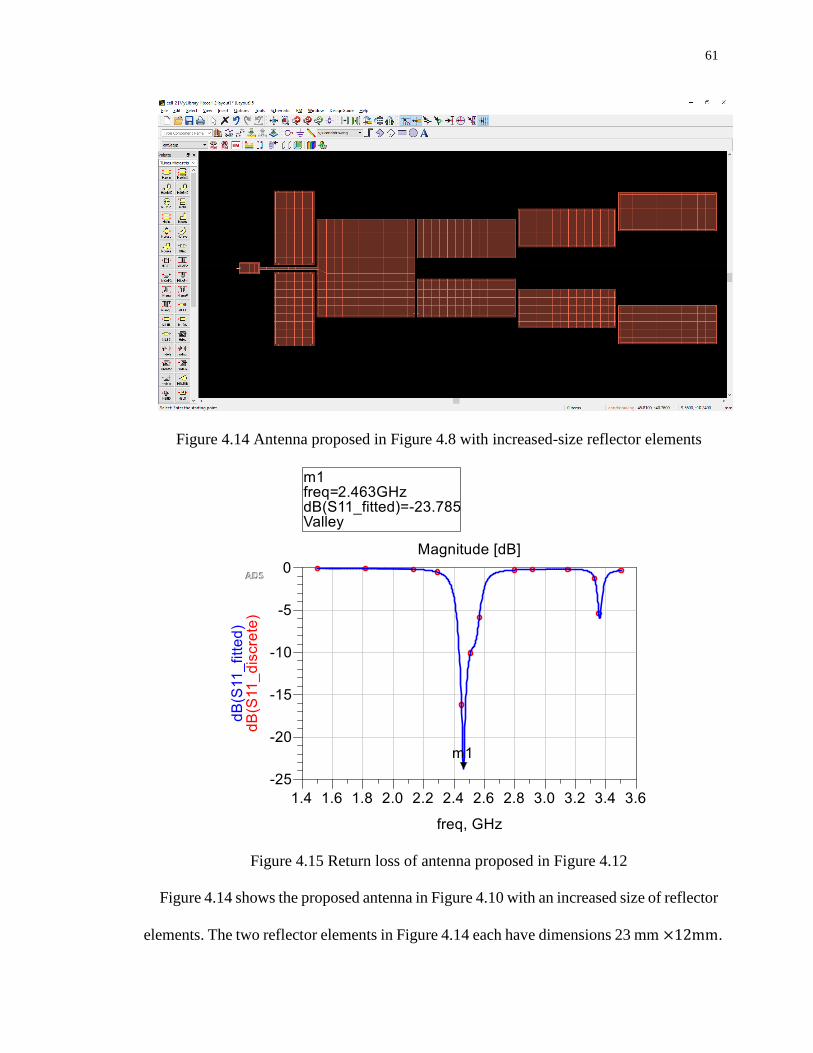
61
Figure 4.14 Antenna proposed in Figure 4.8 with increased-size reflector elements
Figure 4.15 Return loss of antenna proposed in Figure 4.12
Figure 4.14 shows the proposed antenna in Figure 4.10 with an increased size of reflector
elements. The two reflector elements in Figure 4.14 each have dimensions 23 mm ×12mm.

62
As shown in Figure 4.15, with the increased size of reflector elements, the resonant
frequency shifts to 2.463 GHz from 2.460 GHz.
In conclusion, the frequency reconfigurability must be achieved by considering both the
impact of parasitic elements and the slot. The frequency shift caused by the increased size
of reflector and director is much smaller than frequency shift caused by slot.
(3) Our Method to Achieve Frequency Reconfigurable
Recall that in PASS theory, if the frequency ratio of two different working frequencies
becomes larger, the PASS design may not get a good match for both modes, and slot
implementations need to be carefully considered. For our proposed Yagi-Uda patch
antenna, the two expected working frequencies are 1.9GHz and 2.4 GHz, and the frequency
ratio is 2.4/1.9 = 1.26. It is difficult to find a good match point for two modes by using only
one slot. We chose to use two switchable slots in the antenna to obtain a good match for
both modes and proved this is an effective method. The greatest challenge is finding a
commonly matched position for both the switch’s ON and OFF modes under the effect of
parasitic elements. Because input impedance can be vary greatly with different modes, this
method required many simulations.
A common good matching point is dependent on the dimensions of two slots and their
positions. A great number of simulations have been carried out to find the proper
parameters.

63
Figure 4.16 shows the final design for the proposed pattern and frequency reconfigurable
Yagi-Uda patch antenna. Based on our simulations, the gap (G3) between two slots has
been set to 10.5 mm, the distance (L5) between slot and radiation edge has been set to 18
mm. The corresponding parameters are shown in Figure 4.16. The size of the two slots has
been set to 22.3mm ×1mm (W2×G1). The size of the six director elements are set to be
30.5mm × 40mm (W5×L4), and the size of two reflectors are be set to 18mm ×10.5mm
(W4×L3). The size of driven element has been adjusted to 48.5mm ×29.5mm.
Figure 4.16 Geometry of Proposed Reconfigurable Yagi-Uda Patch Antenna
L5
G2
H1
W5
W3
G2
G1 G2
G2
W4
L3
W5 W5
L4
L4
H2 H3
G3
L5
W2

64
Figure 4.17 Layout simulation for proposed antenna with four metal pieces
Figure 4.18 Simulated return loss for proposed antenna with four metal pieces
Metal Pieces
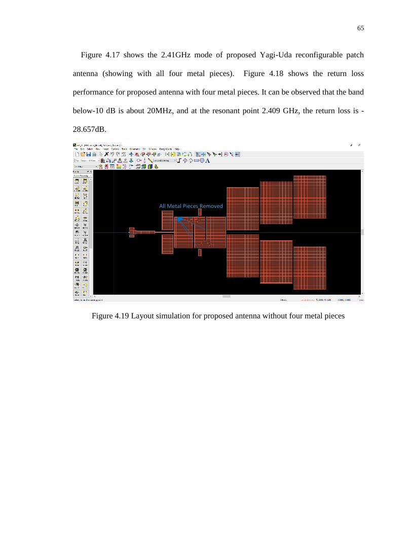
65
Figure 4.17 shows the 2.41GHz mode of proposed Yagi-Uda reconfigurable patch
antenna (showing with all four metal pieces). Figure 4.18 shows the return loss
performance for proposed antenna with four metal pieces. It can be observed that the band
below-10 dB is about 20MHz, and at the resonant point 2.409 GHz, the return loss is -
28.657dB.
Figure 4.19 Layout simulation for proposed antenna without four metal pieces
All Metal Pieces Removed
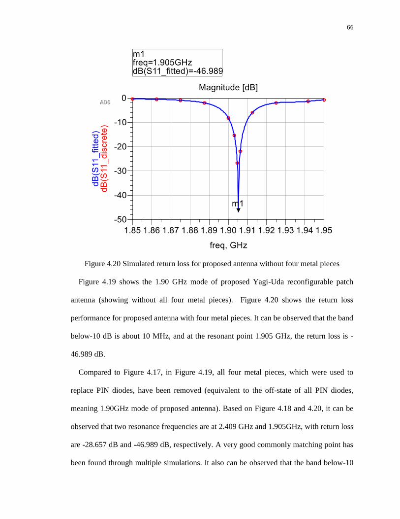
66
Figure 4.20 Simulated return loss for proposed antenna without four metal pieces
Figure 4.19 shows the 1.90 GHz mode of proposed Yagi-Uda reconfigurable patch
antenna (showing without all four metal pieces). Figure 4.20 shows the return loss
performance for proposed antenna with four metal pieces. It can be observed that the band
below-10 dB is about 10 MHz, and at the resonant point 1.905 GHz, the return loss is -
46.989 dB.
Compared to Figure 4.17, in Figure 4.19, all four metal pieces, which were used to
replace PIN diodes, have been removed (equivalent to the off-state of all PIN diodes,
meaning 1.90GHz mode of proposed antenna). Based on Figure 4.18 and 4.20, it can be
observed that two resonance frequencies are at 2.409 GHz and 1.905GHz, with return loss
are -28.657 dB and -46.989 dB, respectively. A very good commonly matching point has
been found through multiple simulations. It also can be observed that the band below-10

67
dB is about 20MHz in Figure 4.18 and the band below-10 dB is about 10 MHz in Figure
4.20.
Figure 4.21 Surface Current Distribution for Antenna Working at 2.41GHz
Figure 4.22 Surface Current Distribution for Antenna Working at 1.90GHz

68
Figure 4.21 and 4.22 show the surface current distribution for proposed antenna at two
working frequencies. The effect of these slots and metal pieces can be observed from these
two figures.
4.2.3 Pattern reconfigurable of proposed Yagi-Uda antenna
In early simulations, designs were found which worked at both required frequencies, as
shown in Figures 4.23 and 4.26. However, the pattern and directivity for each of them were
not good.
Figure 4.23 Early design of the proposed 2.41 GHz antenna

69
Figure 4.24 Return loss of early 2.41 GHz design
Figure 4.25 Pattern for the early 2.41 GHz design

70
Figure 4.26 Early design of the proposed 1.90 GHz antenna
Figure 4.27 Return loss of early 1.90 GHz design

71
Figure 4.28 Pattern for the early 1.90 GHz design
From the theory of Yagi-Uda antennas, the directors are responsible for increasing the
directivity of antenna. Patterns in Figures 4.25 and 4.28 show that the directors did not
work well. The size of six director elements were changed. After many simulations, we
increased the size of each of six director elements from 30.5 mm ×14mm to 30.5 mm ×
40 mm for the final Design, as shown in Figures 4.15 and 4.18.
Figure 4.29 (1) (2) shows the simulated radiation patterns of the final design at 2.41GHz
and 1.90 GHz. Figure 4.30 shows the simulated intensity of the final design at 2.41GHz
and 1.90 GHz . Radiation intensity in a given direction is defined as the power radiated
from an antenna per unit solid angle. (The radiation intensity is a far-field parameter which
can be obtained by simply multiplying the radiation density by the square of the distance:
U = 𝑅2×𝑊𝑟𝑎𝑑.) Table 4.2 shows all the related parameters at the two resonant frequencies
of 2.41 GHz and 1.90 GHz in simulations . It can be seen from Figure 4.29 (1) (2) that the
patterns of different working frequencies are different. From Table 4.2, we can see the

72
differece of main beam direction steering (azimuth angle-φ, elevation angle-θ) for different
working frequencies.
TABLE 4.2 RADIATION PARAMETERS OF THE PROPOSED ANTENNA
Frequency E_MAX(c/n) Theta_Max(Degree) Phi_Max(Degree) Directivity_Max(dBi)
1.90GHz 0.482 10.000 354.000 8.159
2.41GHz 0.711 65.000 1.000 9.596
(1) Radiation pattern of 2.41GHz for proposed antenna
(2) Radiation pattern of 1.90 GHz for proposed antenna
Figure 4.29 Radiation patterns of 2.41GHz and 1.90GHz for proposed antenna

73
(1) Radiation Intensity for 2.41 GHz
(2) Radiation intensity for 1.90 GHz
Figure 4.30 Radiation intensity for two working frequencies

74
4.2.4 Using of stubs for 2.41GHz
Narrow bandwidth is the serious limitation of microstrip antenna. An effective way of
bandwidth enhancement is to load the surface patch by stubs. In [45], by attaching a pair
of tuning stubs to the feedline to introduce an additional resonance in the high frequency
range, bandwidth enhancement for broadband operation can be obtained. In [46], in order
to further increase the BW, stub-loaded variations of a hexagonal patch was presented. In
[47], a novel wideband aperture coupled microstrip antenna consists of radiating patch with
stubs and a cross microstrip feed line is presented. The operating relative bandwidth of
antenna of 41% is achieved with higher antenna efficiency and stable radiation patterns are
realized also. By changing the dimension of the stub attached to the patch, the variable
reactance may be realized. Usually, the capacitance of the open ended stub increases due
to increase in the length. Short open-circuited stubs can also be used as load to adjust the
operating frequency of patch antennas.
Two open-end stubs with optimized lengths and widths are involved to be loaded at the
driven patch of the proposed Yagi-Uda patch antenna exclusively to adjust the impedance
and bandwidths together, as shown in Figure 4.31. They were connected to the driven
element by using metal pieces at 2.41GHz working frequency. Those metal pieces, used to
replace PIN diodes in simulation, were removed when the proposed antenna was working
at 1.90GHz (Shown in Figure 4.18). The dimensions of these two stubs are set to 2.72mm
× 6.5mm (W3×L2), based on our simulations.
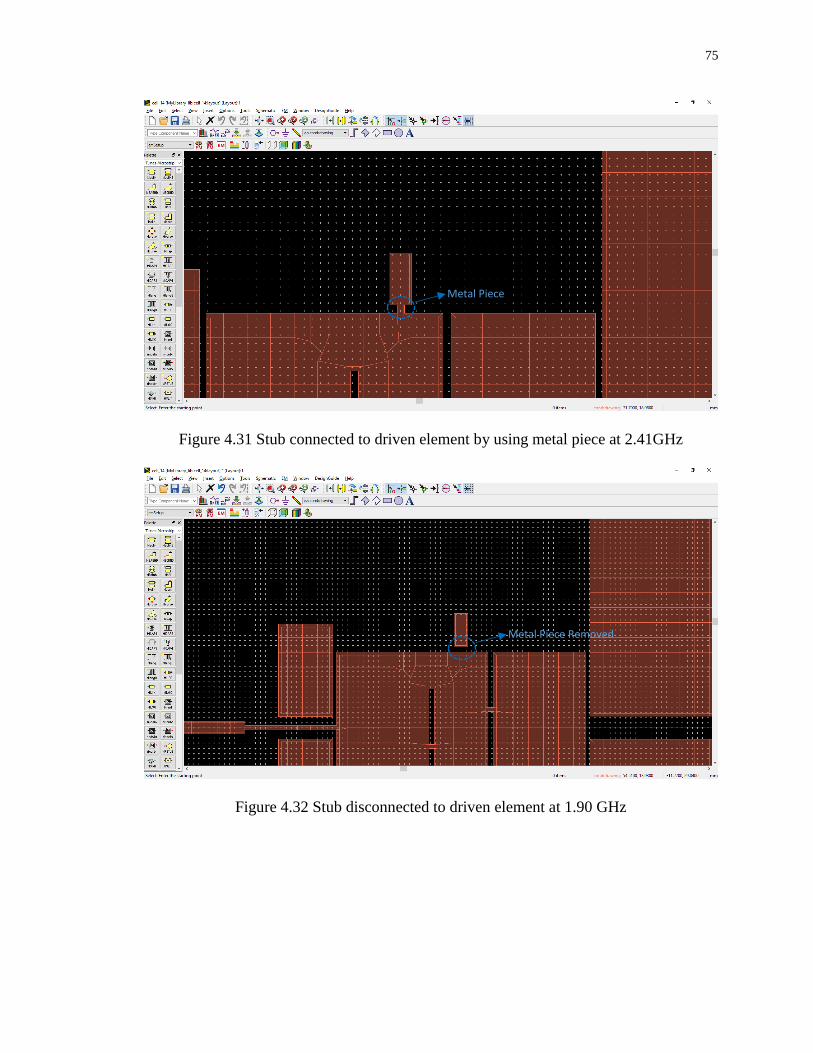
75
Figure 4.31 Stub connected to driven element by using metal piece at 2.41GHz
Figure 4.32 Stub disconnected to driven element at 1.90 GHz
Metal Piece
Metal Piece Removed

76
Figure 4.33 Return loss for proposed antenna working at 2.41GHz
Figure 4.34 Without two pieces of metal used to connect stubs and driven element

77
Figure 4.35 Return loss for proposed antenna with 2 metal pieces that used to connect
stubs and driven pieces have been removed
For the antenna configuration which works in 2.41 GHz, if we remove those two stubs,
the difference of return loss performance can be observed from Figure 4.33 and Figure 4.35.
In figure 4.33, the bandwith below -10 dB is about 20 MHz while the bandwith below -10
dB is about 12 MHz in Figure 4.35. The stubs we used incresased the bandwith of the
proposed antenna by about 67%. For the antenna working at 1.90 GHz, we did not use
broadband technology. Future studies will investigate broadband technology, which can be
used at both 2.14 GHz and 1.90 GHz.

78
4.3 Fabrications and Measurements of the Proposed Reconfigurable Yagi-
Uda patch Antenna
We used a T Tech mill machine (Figures 4.36-4.38) to build our proposed reconfigurable
Yagi-Uda patch antenna. The measurement works have been done by using Agilent
E5062A Network Analyzer.
Figure 4.36 The T Tech mill machine used to build the proposed antenna

79
Figure 4.37 The T Tech mill machine controlled by a computer
Figure 4.38 Milling device of T Tech Mill Machine
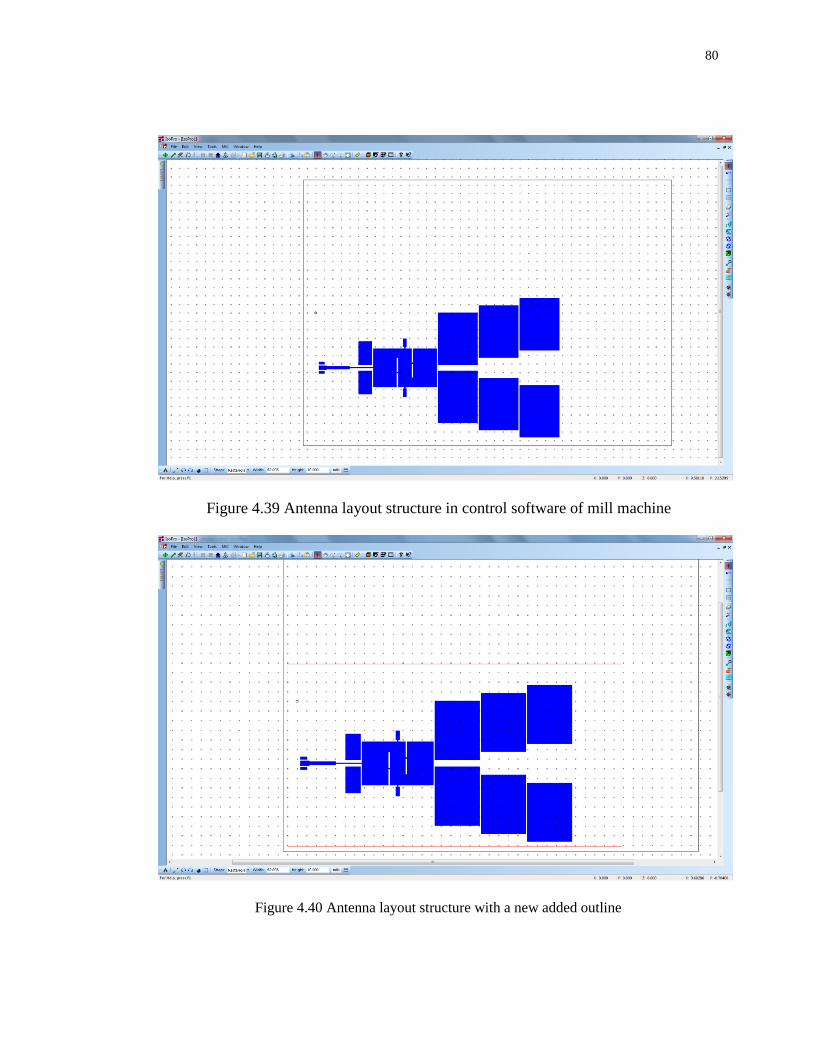
80
Figure 4.39 Antenna layout structure in control software of mill machine
Figure 4.40 Antenna layout structure with a new added outline
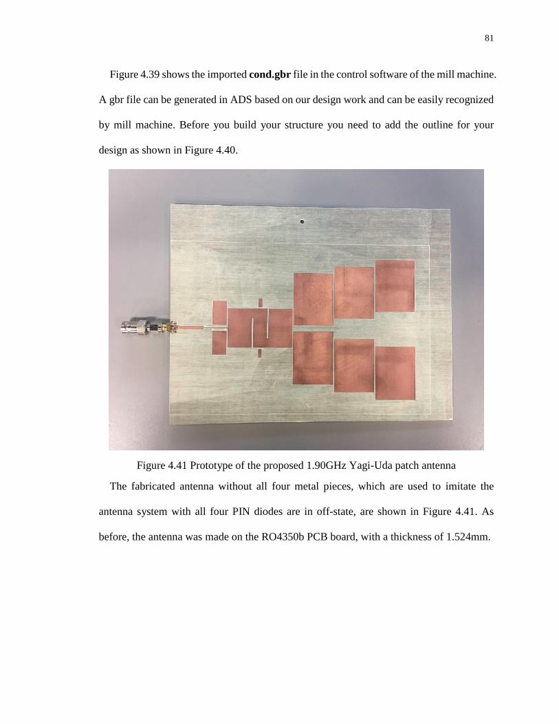
81
Figure 4.39 shows the imported cond.gbr file in the control software of the mill machine.
A gbr file can be generated in ADS based on our design work and can be easily recognized
by mill machine. Before you build your structure you need to add the outline for your
design as shown in Figure 4.40.
Figure 4.41 Prototype of the proposed 1.90GHz Yagi-Uda patch antenna
The fabricated antenna without all four metal pieces, which are used to imitate the
antenna system with all four PIN diodes are in off-state, are shown in Figure 4.41. As
before, the antenna was made on the RO4350b PCB board, with a thickness of 1.524mm.

82
Figure 4.42 Measurement of prototype 1.90GHz Yagi-Uda patch antenna (1)
Figure 4.43 Measurement of prototype 1.90GHz Yagi-Uda patch antenna (2)
Figures 4.42 and 4.43 show the measuring process for the built 1.90 GHz mode antenna.
The electronic device used in figure 4.42 and 4.43 is Agilent E5062A Network Analyzer.

83
Figure 4.44 Measurement result for 1.90GHzYagi-Uda patch antenna
Figure 4.45 Prototype of the proposed 2.41GHz Yagi-Uda Patch Antenna
The fabricated antenna with all four metal pieces that were used to imitate the antenna
system with all four PIN diodes in the ON state, is shown in Figure 4.45. It was also made
on the RO4350b PCB board with the thickness of 1.524 mm.

84
Figure 4.46 Measurement of the prototype 2.41GHz Yagi-Uda patch antenna (1)
Figure 4.47 Measurement of the prototype 2.41GHzYagi-Uda patch antenna (2)

85
Figure 4.46 and 4.47 show the measuring process for the built 2.41 GHz mode antenna.
The electronic device used, shown in Figures 4.46 and 4.47, is also the Agilent E5062A
Network Analyzer.
Figure 4.48 Measurement result for 2.41 GHz Yagi-Uda patch antenna
Based on Figures 4.44 and 4.48, the measured performance of return loss for two
configurations of the proposed antenna can be observed. For antenna configuration which
has been designed working at 2.41GHz, the resonant frequency of built antenna is 2.428
GHz, and the measured bandwidth below -10 dB is about 20 MHz. For the antenna
configuration that was designed working at 1.90GHz, the measured return loss is about -
23 dB at 1.908 GHz and the measured bandwidth below -10 dB is about 10 MHz. Because
we did not apply broadband technology to this antenna configuration, the measured
bandwidth below -10 dB is about 10 MHz.

86
4.4 Discussions
The comparisons of return loss performance between simulation and measurement are
shown in Figures 4.49 and 4.50.
Figure 4.49 Simulation and Measurement results for proposed antenna without all four
metal pieces (Design working frequency is 1.90 GHz)
It can be observed from Figure 4.49 that the frequency shift between simulation and
measurement for the proposed antenna without four metal pieces is very small (within 3
MHz). The measured return loss is about -23 dB at 1.908 GHz and the measured bandwidth
below -10 dB is about 10 MHz.

87
Figure 4.50 Simulation and Measurement results for proposed antenna with all four metal
pieces (Design working frequency is 2.41 GHz)
It can be observed from Figure 4.50 that the frequency shift between simulation and
measurement for the proposed antenna with four metal pieces is about 18 MHz. The
measured return loss is about -35 dB at 2.428 GHz and the measured bandwidth below -10
dB is about 20 MHz.
The reason for 18 MHz frequency shift in 2.41 GHz design has been analyzed by follows:
(1) For the 2.41 GHz design simulation, the positions of two metal pieces which have
been loaded in two slots must be very accurate. As can be observed from Figure 4.51,
the distance (As H in Figure 4.51) from each of those two metal pieces to top border
and bottom border of the slot was set to be 10.7 mm. And the positions of those two
metal pieces have been got based on a lot of simulations.
(2) If we move the metal piece which loaded in the right slot of the driven element up
for 1mm (As shown in Figure 4.52), the resonant point will shift to 2.434 GHz (As
shown in Figure 4.53).

88
Figure 4.51 The layout structure for proposed antenna
Figure 4.52 The proposed antenna with the metal piece loaded in the right slot has been
moved up 1mm
G2
H1
W5
W3
G2
G1 G2
G2
W4
L3
W5 W5
L4
L4
H2 H3 H
H H
H
Move Up for
1mm

89
Figure 4.53 The resonant point shift to 2.434 GHz based on the change has been made in
figure 4.52
(3) If we move the metal piece which loaded in the right slot of the driven element down
for 1mm (As shown in Figure 4.54), the resonant point will shift to 2.385 GHz (As
shown in Figure 4.55).
(4) The resonant point of this antenna is very sensitive to the dimension of those two
metal pieces loaded in two slots. Based on simulation works, we made the dimension
of all four metal pieces as 0.9mm (height) × 1mm (width). If we increase the height
of those two pieces which loaded in two slots by 0.2 mm (As shown in Figure 4.56),
the resonant point will shift to 2.424GHz. If we decrease the height of those two
pieces which loaded in two slots by 0.2 mm (As shown in Figure 4.58), the resonant
point will shift to 2.393 GHz.

90
Figure 4.54 The proposed antenna with the metal piece loaded in the right slot has been
moved down for 1mm
Figure 4.55 The resonant point shift to 2.385 GHz based on the change has been made in
figure 4.54
Move Down
for 1mm

91
Figure 4.56 The proposed antenna with the height of metal pieces loaded in slots has been
increased by 0.2 mm
Figure 4.57 The resonant point shift to 2.424 GHz based on the change has been made in
figure 4.56
Height=1.1mm
Height=1.1mm

92
Figure 4.58 The proposed antenna with the height of metal pieces loaded in slots has been
decreased by 0.2 mm
Figure 4.59 The resonant point shift to 2.393 GHz based on the change has been made in
figure 4.58
Height=0.7mm
Height=0.7mm

93
We used a T Tech Mill machine to build the proposed antenna. During the fabrication
process, there has to be error of metal pieces, and the resonant point is very sensitive to the
position and dimension of those two metal pieces which are loaded in the slots. This can
explain the 18 MHz frequency shift for 2.41 GHz design. For 1.90 GHz design, because
there are no metal pieces loaded in the slots, the frequency shift is very small (around 3
MHz). Despite the frequency, this antenna can still be used for Wi-Fi systems (Band 4 or
Band 5 of the 2.4 GHz band channel). Considering our fabrication conditions, our results
were quite successful.
4.5 Summary of the Proposed Yagi-Uda Antenna
In this chapter, a novel Yagi-Uda reconfigurable patch antenna was proposed. Two slots
have been used on the driven element of this antenna system to create frequency and pattern
reconfigurability and we use metal pieces to replace PIN diodes in the simulation and
measurement. Pattern reconfigurability and directivities with all over 8.1 dBi in both main
radiation directions have been found on two different working frequencies in simulation.
The measured bandwidth of the return loss below -10dB for 2.41GHz working mode is
about 20 MHz and for the 1.90 GHz working mode is 10 MHz. The simulation and
measurement for return loss results closely agree. The slight frequency shifts are due to
fabrication error. This pattern and frequency reconfigurable Yagi-Uda patch antenna array
can be applied for both LTE and Wi-Fi systems.

94
Chapter 5. Conclusions
In chapter 3, a novel dual-frequency antenna array with multiple pattern selectivities is
proposed. We used a single-feed switchable network as a basic beam pattern
reconfigurability structure for this dual-frequency antenna array. The slotted corners on the
patch together with the states of PIN diodes gave this antenna array more freedom of
pattern changeability. The measured bandwidth of the return loss below -10dB for the on-
state is about 25 MHz and for the off-state is also nearly 25 MHz at two different working
frequencies, respectively. We have validated this structure is effective to introduce more
pattern selectivity. This pattern reconfigurable patch antenna array can be applied in the
wideband code division multiple access system.
In chapter 4, a novel Yagi-Uda patch antenna with frequency and pattern selectivity was
proposed. Our proposed antenna consists of two reflector elements, a driven element and
six director elements. Two open-end stubs, which were used to improve the return loss
performance and adjust working frequency, were connected to the driven element when it
was working at 2.41 GHz. In order to easily validate our design, we used four metal pieces
to imitate different states of PIN diodes in simulation and measurement. We built two
proposed Yagi-Uda patch antennas, one with and one without, metal pieces. For the built
antenna without metal pieces, the measured return loss is about -23 dB at 1.908 GHz and
the measured bandwidth below -10 dB is about 10 MHz. For the built antenna with four
metal pieces, the measured return loss is about -35 dB at 2.428 GHz and the measured
bandwidth below -10 dB is about 20 MHz. The frequency shifts are mainly attributed to
the fabrication error. Basically, the simulation and measurement results agreed well. The
pattern of the proposed antenna is different between two working frequencies but with the

95
directivity all above 8 dBi. The effectiveness of this kind of antenna structure has been
validated by this study. It can be both frequency and pattern reconfigurable. This proposed
Yagi-Uda reconfigurable patch antenna can be used in both LTE and Wi-Fi systems.

96
References
[1] Wenquan Cao, Bangning Zhang, Aijun Liu, Tongbin Yu, Daosheng Guo, and Kegang
Pan, “A reconfigurable microstrip antenna with radiation pattern selectivity and
polarization diversity,” IEEE Antenna and Wireless Propagation Letters,Vol.11,pp.
453-456, 2012.
[2] H. M. Lee, “Pattern reconfigurable micro-strip patch array antenna using switchable
feed-network,” Proceedings of Asia-Pacific Microwave Conference 2010, FREG-12.
[3] S. L. S. Yang and K. M. Luk, “Design a wide-band L-probe patch antenna for pattern
reconfigurable or diversity applications,” IEEE Trans. Antennas Propag., vol. 54, no.
2, pp. 433–438, Feb. 2006.
[4] L. Low and R. J. Langley, “Single-feed antenna with radiation pattern diversity,”
Electron. Lett, vol. 40, No.16, Aug. 5, 2004.
[5] L. Petit, L. Dussopt, and J.-M. Laheurte, “MEMS-switched parasitic antenna array
for radiation-pattern diversity,” IEEE Trans. Antennas Propag., vol. 54, no. 9, pp.
2624–2631, Sep. 2006.
[6] D.kornek, J.Meyer, C.Orlob, I. Rolfes, “Reconfigurable triangular patch antenna for
pattern diversity,” EuCAP 2009. 3rd European Conference on Antennas and
Propagation, pp 3744-3747.
[7] Yan-Ying Bai, Shaoqiu Xiao, Changrong Liu, Xiang Shuai, and Bing-Zhong Wang,
“Design of pattern reconfigurable antennas based on a two-element dipole array model,”
IEEE Transactions on Antennas and Propagation, vol.61,Issue.9, Pages: 4867 – 4871,
2013.

97
[8] Hai Liang Zhu, Sing Wai Cheung, Tong lp Yuk, “Mechanically pattern
reconfigurable antenna using metasurface,” IET Microwaves, Antenna and
Propagation, Volume.9, Issue.12,Pages: 1331 – 1336,2015.
[9] Mei Li, Shaoqiu Xiao, Bingzhong Wang, “Compact, low-profile, HIS-based pattern
reconfigurable antenna for wide-angle scanning,” The 8th European Conference on
Antennas and Propagation (EuCAP 2014), Pages: 1541 – 1544.
[10] Dwi Andi Nurmantris, Heroe Wijanto, Bambang Setia Nugroho, “A pattern
reconfigurable of circular short-circuited patch antenna based on Genetic Algorithm,”
2014 2nd International Conference on Information and Communication Technology
(ICoICT), pp 351-355.
[11] Jeen-Sheen Row and Jia-Fu Tsai, “Frequency-reconfigurable microstrip patch
antennas with circular polarization,” IEEE Antennas And Wireless Propagation
Letters,VOL.13, pp 1112-1115, 2014.
[12] Qiang Liu, Naizhi Wang, Qingsheng Zeng, Changying Wu, Gao Wei, “A frequency
reconfigurable patch antenna with reed switches,” 2014 IEEE International Wireless
Symposium (IWS).
[13] Chao Sun, Huili Zheng, Lingfei Zhang, and Ying Liu, “A compact frequency-
reconfigurable patch antenna for beidou (COMPASS) navigation system,” IEEE
Antennas And Wireless Propagation Letters,VOL.13, pp 967-970, 2014.
[14] I.Rouissi, J.M.Floc’h, H.Rmili, H.Trabelsi, “Design of a frequency reconfigurable
patch antenna using capacitive loading and varactor diode,” 2015 9th European
Conference on Antennas and Propagation (EuCAP).

98
[15] M. A. Aris, M. T. Ali, N. H. Abd. Rahman, N. Ramli, “Frequency reconfigurable
aperture-coupled microstrip patch antenna using defected ground structure,” 2015
IEEE International RF and Microwave Conference (RFM 2015), pp 200-204.
[16] R. Kanimozhi, P. Jothilakshmi, “A high frequency-reconfigurable multilayer
microstrip patch antenna (HFRMPA),” International Conference on Communication
and Signal Processing, pp 480-484, April 3-5, 2014, India.
[17] Lei Ge, and Kwai-Man Luk, “Frequency-reconfigurable low-profile circular
monopolar patch antenna,” IEEE Transaction Antennas and Propagation, Vol.62, No.7,
pp 3443-3449, July 2014.
[18] N. Ramli, M. T. Ali, A. L. Yusof, S. Muhamud - Kayat, and A. A. A. Aziz, “PIN
diode switches for frequency-reconfigurable stacked patch microstrip array antenna
using aperture-coupled technique,” 2013 Asia-Pacific Microwave Conference
Proceedings, pp 1052-1054.
[19] Ratnesh Kumari, Mithilesh Kumar, “Compact tri band frequency reconfigurable L-
slot octagonal shape patch antenna,” 2013 5th International Conference on
Computational Intelligence and Communication Networks, pp 64-69.
[20] Jeen-Sheen Row and Ting-Yi Lin, “Frequency-reconfigurable coplanar patch
antenna with conical radiation,” IEEE Antennas And Wireless Propagation Letters,
VOL. 9, pp 1088-1091, 2010.
[21] Zi-Xian Yang, Hong-Chun Yang, Jing-Song Hong, and Yang Li, “Bandwidth
enhancement of a polarization-reconfigurable patch antenna with stair-slots on the
ground,” IEEE Antennas And Wireless Propagation Letters, VOL. 13, pp 579-582,
2014.

99
[22] Xue-Xia Yang, Bing-Cheng Shao, Fan Yang, Atef Z. Elsherbeni,and Bo Gong, “A
polarization reconfigurable patch antenna with loop slots on the ground plane,” IEEE
Antennas And Wireless Propagation Letters, VOL. 11, pp 69-72, 2012.
[23] Hucheng Sun, Sheng Sun, “A polarization-agile aperture-coupled patch antenna
using quad-mode reconfigurable feeding network,” 2016 IEEE MTT-S International
Microwave Workshop Series on Advanced Materials and Processes for RF and THz
Applications (IMWS-AMP).
[24] Hui Gu, Jianpeng Wang, Lei Ge, and Chow-Yen-Desmond Sim, “A new quadri-
polarization reconfigurable circular patch antenna,” IEEE Access, Digital Object
Identifier 10.1109/ACCESS.2016.2600250.
[25] Nghia Nguyen-Trong, Leonard Hall, and Christophe Fumeaux, “A frequency- and
polarization-reconfigurable stub-loaded microstrip patch antenna,” IEEE Transaction
On Antennas And Propagation, Vol. 63, No. 11, pp 5235-5240, November 2015.
[26] Xue-Xia Yang, Bo Gong, Fang Yang, Atef Z. Elsherbeni, “A reconfigurable patch
antenna with quadri-polarization states using dual feed ports,” 978-1-4673-0462-7/12,
2012 IEEE.
[27] Constantine A. Balanis, “Antenna Theory: Analysis And Design,” Second Edition,
John Wiley&Sons, INC.
[28] D. Orban and G.J.K Moernaut, “The Basics of Patch Antennas, Updated,” Orban
Microwave Products, www.orbanmicrowave.com.
[29] D. M. Pozar, “Microstrip Antennas,” Proc. IEEE, Vol. 80, NO. 1, pp. 79-81,
January 1992.

100
[30] N. K. Uzunoglu, N. G. Alexopoulos, and J. G. Fikioris, “Radiation properties of
microstrip dipoles,” IEEE Transaction and Propagation, Vol. AP-27, NO. 6, pp. 853-
858, Novenber 1979.
[31] I. E. Rana and N. G. Alexopoulos, “Current distribution and input impedance of
printed dipoles,” IEEE Transaction. Antenna And Propagation, Vol. AP-29, No. 1, pp.
99-105, January 1981.
[32] P. B. Katehi and N. G. Alexopoulos, “On the modeling of electromagnetically
coupled microstrip antenna-the printed strip dipole,” IEEE Transaction. Antenna And
Propagation, Vol. AP-32, No. 11, pp. 1179-1186, November 1984.
[33] D. M. Pozar, “Analysis of finite phased arrays of printed dipoles,” IEEE
Transaction. Antenna And Propagation, Vol. AP-33, No. 10, pp. 1045-1053, October
1985.
[34] C. A. Balanis, “Advanced Engineering Electromagnetics,” John Wiley & Sons,
New York, 1989.
[35] E. O. Hammerstad, “Equations for microstrip circuit design,” Proc. Fifth European
Microwave Conference, pp. 268-272, Sepetember 1975.
[36] I. J. Bahl and P. Bhartia, “Microstrip Antennas,” Artech House, Dedham, MA, 1980.
[37] J.Huang; “Planar microstrip Yagi array antenna,” IEEE AP-S symposium Digest
June 1989, pp 894-897.
[38] Chen, C. A. and D. K Cheng, “Optimum element lengths for Yagi-Uda arrays,”
IEEE Trans. Antennas and Propagation, Vol. 23, Jan. 1975.

101
[39] M. Bemani and S. Nikmehr, “A novel wide-band microstrip Yagi-Uda array
antenna for WLAN applications,” Progress In Electromagnetics Research B, Vol. 16,
389–406, 2009.
[40] Xue-Song Yang, Bing-Zhong Wang,Weixia Wu, and Shaoqiu Xiao, “Yagi patch
antenna with dual-band and pattern reconfigurable characteristics,” IEEE Aantennas
and Wireless Propagation Letters, Vol. 6, pp 168-171, 2007.
[41] T. Sabapathy, R.B. Ahmad, M. Jusoh, M. R. Kamarudin4, “The effect of shorting
pin locations on the performance of a pattern reconfigurable Yagi-Uda patch antenna,”
2014 2nd International Conference on Electronic Design (ICED), August 19-21, 2014,
Penang, Malaysia.
[42] Jian Zhang, Xue-Song Yang, Jia-Lin Li, and Bing-Zhong Wang, “A linear phased
array with reconfigurable dynamic Yagi-Uda patch antenna elements,” 2012
International Workshop on Microwave and Millimeter Wave Circuits and System
Technology (MMWCST).
[43] Thennarasan Sabapathy, Muzammil Jusoh, R. Badlishah Ahmad, Muhammad
Ramlee Kamarudin, and Ping Jack Soh, “A ground-plane-truncated, broadly steerable
Yagi–Uda patch array antenna,” IEEE Antennas and Wireless Propagation
Letters,Vol.15, pp 1069-1072, 2016.
[44] Fan Yang and Yahya Rahmat-Samii, “Patch antennas with switch slots (PASS) in
wireless communications: concepts, designs, and applications,” IEEE Antennas and
Propagation Magazine, Vol. 47, No. 2, pp13-29, April 2005.

102
[45] Oteng Gyasi Kwame, Wen Guangjun, Xue Xiao Lin, Muhammad Abdul Basit,
“Bandwidth enhancement of a microstrip-line-fed printed rotated wide slot antenna
with tuning stubs,” 2016 IEEE MTT-S International Wireless Symposium (IWS).
[46] Amit Deshmukh, Sudesh Agrawal, Kshitij Lele, K. P. Ray, “Broadband CPW fed
stub loaded hexagonal slot backed hexagonal microstrip antenna,” 2015 International
Conference on Microwave and Photonics (ICMAP).
[47] Youbao Wang , Yaming Bo and De Ben, “Wideband aperture coupled microstrip
antenna with stubs,” The 2006 4th Asia-Pacific Conference on Environmental
Electromagnetics, pp 682-684.
Copyright © 2022 FDOKUMEN