IMPLEMENTATION OF CFDA METHOD FOR MATCHING INFRARED AND OPTICAL FACE IMAGE
Upload
khangminh22Category
view
0download
0
applied sciences
Article
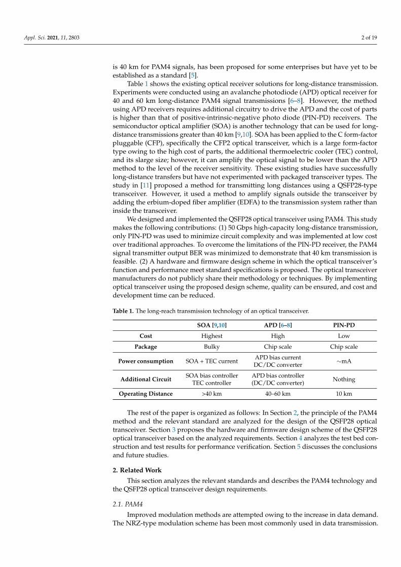
Design and Implementation Scheme of QSFP28 OpticalTransceiver for Long-Reach Transmission UsingPAM4 Modulation dagger
Jae-Woo Kim 1Dagger Dong-Seong Kim 2 Seung-Hwan Kim 1 and Sang-Moon Shin 3Dagger
Citation Kim J-W Kim D-S Kim
S-H Shin S-M Design and
Implementation Scheme of QSFP28
Optical Transceiver for Long-Reach
Transmission Using PAM4 Modulation
Appl Sci 2021 11 2803 https
doiorg103390app11062803
Academic Editor Nikos Pleros
Received 2 February 2021
Accepted 16 March 2021
Published 21 March 2021
Publisherrsquos Note MDPI stays neutral
with regard to jurisdictional claims in
published maps and institutional affil-
iations
Copyright copy 2021 by the authors
Licensee MDPI Basel Switzerland
This article is an open access article
distributed under the terms and
conditions of the Creative Commons
Attribution (CC BY) license (https
creativecommonsorglicensesby
40)
1 ICT Convergence Research Center Kumoh National Institute of Technology Gumi 39177 Gyeongbuk Koreajaewookimkumohackr (J-WK) ksh001kumohackr (S-HK)
2 Department of IT Convergence Engineering Kumoh National Institute of TechnologyGumi 39177 Gyeongbuk Korea
3 Coset Inc PyeongChang 2321 Gangwon Korea sangmoonshingmailcom Correspondence dskimkumohackrdagger Fabrication of 53 Gbs Optical Transceiver over 40-km transmission with PAM4 modulation In Proceedings
of the 2019 21st International Conference on Advanded Communication Technology (ICACT) PyeongChangKorea 17ndash20 February 2019
Dagger These authors contributed equally to this work
Abstract A quad small form-factor pluggable 28 Gbps optical transceiver design scheme is proposedIt is capable of transmitting 50 Gbps of data up to a distance of 40 km using modulation signalswith a level-four pulse-amplitude The proposed scheme is designed using a combination of electro-absorption-modulated lasers transmitter optical sub-assembly low-cost positive-intrinsic-nativephotodiodes and receiver optical sub-assembly to achieve standard performance and low costMoreover the hardware and firmware design schemes to implement the optical transceiver arepresented The results confirm the effectiveness of the proposed scheme and the performance of themanufactured optical transceiver thereby confirming its applicability to real industrial sites
Keywords PAM4 QSFP28 optical transceiver PCB design firmware design
1 Introduction
Recent new technologies such as fifth-generation wireless networks (5G) artificialintelligence (AI) virtual reality (VR) the Internet of things (IoT) and self-driving carsrequire a large bandwidth and fast response time To support the needs of such newtechnologies the core network is evolving from 100 GE to 400 GE and the research anddevelopment of 400 Gbps optical transceivers continues to progress [1] With increaseddata consumption increased bandwidth is required For this purpose long-distance opticaltransceivers that use a variety of modulation methods such as polarization-multiplexingand quadrature phase-shift-keying (PM-QPSK or DP-QPSK) and quadrant amplitudemodulation (QAM) [2] have been developed However this modulation method requires anexpensive photomultiplier and the corresponding sophisticated technology A commonlyused non-return-to-zero (NRZ) modulation scheme can transmit one bit per symbol Alevel-four pulse-amplitude modulation (PAM4) is advantageous because it can transmittwo bits per symbol twice that of the traditional NRZ [3] However the PAM4 schemehas a characteristic lower bit error rate (BER) because it is more noise-sensitive than theNRZ method Therefore increased caution is required when designing optical transceiversusing PAM4
The Institute of Electrical and Electronics Engineers(IEEE) 8023 cd standard documentdefines the physical layer and associated parameter management of 50 Gbps PAM4 opticaltransmitters and receivers for 50GBASE(Gbs PHYs)-FR (far reach 2 km) and LR (longreach 10 km) [4] However the specification for the longest-distance transmission which
Appl Sci 2021 11 2803 httpsdoiorg103390app11062803 httpswwwmdpicomjournalapplsci
Appl Sci 2021 11 2803 2 of 19
is 40 km for PAM4 signals has been proposed for some enterprises but have yet to beestablished as a standard [5]
Table 1 shows the existing optical receiver solutions for long-distance transmissionExperiments were conducted using an avalanche photodiode (APD) optical receiver for40 and 60 km long-distance PAM4 signal transmissions [6ndash8] However the methodusing APD receivers requires additional circuitry to drive the APD and the cost of partsis higher than that of positive-intrinsic-negative photo diode (PIN-PD) receivers Thesemiconductor optical amplifier (SOA) is another technology that can be used for long-distance transmissions greater than 40 km [910] SOA has been applied to the C form-factorpluggable (CFP) specifically the CFP2 optical transceiver which is a large form-factortype owing to the high cost of parts the additional thermoelectric cooler (TEC) controland its slarge size however it can amplify the optical signal to be lower than the APDmethod to the level of the receiver sensitivity These existing studies have successfullylong-distance transfers but have not experimented with packaged transceiver types Thestudy in [11] proposed a method for transmitting long distances using a QSFP28-typetransceiver However it used a method to amplify signals outside the transceiver byadding the erbium-doped fiber amplifier (EDFA) to the transmission system rather thaninside the transceiver
We designed and implemented the QSFP28 optical transceiver using PAM4 This studymakes the following contributions (1) 50 Gbps high-capacity long-distance transmissiononly PIN-PD was used to minimize circuit complexity and was implemented at low costover traditional approaches To overcome the limitations of the PIN-PD receiver the PAM4signal transmitter output BER was minimized to demonstrate that 40 km transmission isfeasible (2) A hardware and firmware design scheme in which the optical transceiverrsquosfunction and performance meet standard specifications is proposed The optical transceivermanufacturers do not publicly share their methodology or techniques By implementingoptical transceiver using the proposed design scheme quality can be ensured and cost anddevelopment time can be reduced
Table 1 The long-reach transmission technology of an optical transceiver
SOA [910] APD [6ndash8] PIN-PD
Cost Highest High Low
Package Bulky Chip scale Chip scale
Power consumption SOA + TEC current APD bias currentDCDC converter simmA
Additional Circuit SOA bias controllerTEC controller
APD bias controller(DCDC converter) Nothing
Operating Distance gt40 km 40ndash60 km 10 km
The rest of the paper is organized as follows In Section 2 the principle of the PAM4method and the relevant standard are analyzed for the design of the QSFP28 opticaltransceiver Section 3 proposes the hardware and firmware design scheme of the QSFP28optical transceiver based on the analyzed requirements Section 4 analyzes the test bed con-struction and test results for performance verification Section 5 discusses the conclusionsand future studies
2 Related Work
This section analyzes the relevant standards and describes the PAM4 technology andthe QSFP28 optical transceiver design requirements
21 PAM4
Improved modulation methods are attempted owing to the increase in data demandThe NRZ-type modulation scheme has been most commonly used in data transmission
Appl Sci 2021 11 2803 3 of 19
Meanwhile the PAM4 scheme was attempted by a company that created the digital signalprocessing (DSP) integrated circuit (IC) for data modulation [12] Figure 1 shows a com-parison between the NRZ and PAM4 signals Compared with NRZ PAM4 demonstratesnumerous benefits associated with having half the Nyquist frequency These benefits in-clude doubling the data density achieving higher resolution using the same oversamplingrate and having the same total noise power spread over a wider frequency band
Figure 1 Comparison of non-return-to-zero (NRZ) and level-four pulse-amplitude modulation(PAM4) signals [3]
The NRZ modulation scheme encodes a binary pattern such as 0110010 into a con-tinuous sequence of fixed voltage levels of low and high voltages of 0 and 1 respectivelyAssuming a bit rate of 25 Gbps faster bit speeds and higher bandwidths are needed totransmit 50 Gbps which is twice the bit rate To double the bit rate without doublingthe bandwidth the signal level must be split in half and added to the signal Thus thereare four signal levels similar to that of the PAM4 signal and 2 bits per level symbol isassigned Meanwhile the IEEE P8023bj KP4 standard defines the requirements for 28Gbps PAM4 signals whereas the IEEE P8023bs andOptical Internetworking forum(OIF)CEI-56G-PAM4 documents define standards for 56 Gbps PAM4 signals [1314]
22 QSFP28 Optical Transceiver Hardware Standard
The QSFP28 optical transceiver complies with the QSFP multi-source agreement(QSFP-MSA) specification SFF-8665 is a standard document for QSFP28 optical transceiversolutions [15] The QSFP28 specification documents to be referenced for the manufactureof optical transceivers consist of documents on the electrical characteristics of opticaltransceivers instrument specifications such as optical transceiver connectors and sizescage specifications on the host side to operate with inserted optical transceivers andmanagement interface specifications that can be viewed as software specifications TheSFF-8679 specification describes the hardware and electrical characteristics that the QSFP28optical transceiver must fulfill and defines the connector specification for the QSFP28optical transceiver the function of each pin and the interface for the data control andstatus signals of the optical transceiver [16] In addition the electronic static discharge(ESD) specification and the instrument-related specifications of the optical transceiver aswell as the temperature and timing specifications are defined Figure 2 shows the QSFP28optical transceiver and host interface structure proposed in the standard document
The hardware configuration of the QSFP28 optical transceiver consists of a quadoptical transmitter and quad optical receiver for transmission and reception a clock datarecovery (CDR) IC for processing the transmission signals a micro-controller unit (MCU)for operation of the QSFP28 optical transceiver and a host connector for sending andreceiving control and data signals with the host There are up to four channels for data
Appl Sci 2021 11 2803 4 of 19
transmission and reception The functions of control and alarm signals are summarizedin Table 2 The power consumption of the QSFP28 optical transceiver is divided intoeight classes according to the available host system capacity with each class defining themaximum allowable power If the optical transceiverrsquos power consumption exceeds thespecified consumption capacity the QSFP28 optical transceiver is applied with an LPModesignal to enter the low-power state The QSFP28 optical transceiver in a low-power stateshould have a power consumption of less than 15 W Another standard document definestemperature specifications for normal operation of the optical transceiver from a minimumof 0 degC to a maximum of 70 degC based on the QSFP28 optical transceiver case Finally thetiming specification for the response speed of the QSFP28 optical transceiver according tothe hardware control signal of the host and the timing specification for alarm generationare defined
Figure 2 QSFP28 interface block diagram between host system and transceiver [16]
Table 2 Control and alarm signals with host connector for QSFP28 [16]
Name Function
ModPrsL Optical transceiver insertion status to hostSCLSDA Two-wire serial interfaceModSelL Module selection when using multiple modules
ResetL Optical transceiver resetintL Optical transceiver alarm interrupt
RxLOSL Optical transceiver loss of signalLPMode Low power mode enabled
TxDis Disable the optical transmission
Appl Sci 2021 11 2803 5 of 19
23 QSFP28 Optical Transceiver Software Standard
The specifications for the operation and management of QSFP28 optical transceiversare defined in the SFF-8636 document [17] The QSFP28 optical transceiver uses a 2-wirebus interface to communicate with the host The 2-wire bus interface for QSFP28 is the sameas that used in inter-integrated circuit (I2C) communications but with some differences inthe write operation The 2-wire interface does not support a ldquocombined formatrdquo that cansend continuous write addressing for writing Therefore under repeated start conditionsthe firmware should be implemented to discard writing operation and to abort the datareceived Figure 3 shows the procedure for a byte write behavior in the I2C interfacebetween the host and the optical transceiver as defined in the standard Figure 3a is aone-byte write operation and Figure 3b is a sequential byte write operation The hostsystem becomes the master and the QSFP28 optical transceiver is a slave The I2C interfacesends I2C frames in bytes checks the opponentrsquos acknowledgement in the ninth clock andsendsreceives additional data in bytes It should be able to send up to four sequentialbytes in a sequential write operation Detailed procedures for the I2C interface protocolbetween the QSFP28 optical transceiver and the host are defined in the standard document
(a) Write byte operation
(b) Sequential write operation without ldquocombined formatrdquo
Figure 3 QSFP28 host two-wire interface (write operation) [17]
To control the operation of the QSFP28 optical transceiver through the host interfaceand to check the optical transceiver status the QSFP28 optical transceiver configures theinternal register map Figure 4 shows the register map structure defined in the standardThe physical address for accessing the QSFP28 register with the I2C interface is 0 times A0in hexadecimal The QSFP28 register consists of pages and each page consists of 128bytes The register consists of one lower page and a number of upper pages and an upper
Appl Sci 2021 11 2803 6 of 19
page consists of a basic required page and an optional page The address to access theregister lower page and upper page ranges from 0 times 00 to 0 times FF from 0 times 00 to 0times 7F and from 0 times 80 to 0 times FF respectively Data such as interrupt flags and statusmonitoring that require quick access are configured on the lower page for timely accessPage 01 h corresponding to an upper page can implement an application option tableand page 02 h acts as an electrically erasable programmable read-only memory (EEPROM)by allowing users to arbitrarily read and write Pages 20 h to 21 h includes the informationfrom additional monitored parameters for modules that have PAM4 such as alarm andmonitoring parameters This study includes support for additional monitoring parametersfor QSFP28 optical transceivers To access the upper page The host can read or write thevalue to the upper page address after writing the upper page index value to access thelower page address 0 times 7F
Figure 4 QSFP28 internal register architecture and page accessing [17]
3 Proposed Design Scheme31 Hardware Design
Figure 5 shows the complete hardware structure diagram proposed with referenceto the standard documentation The QSFP28 optical transceiver internal hardware of theproposed design scheme consists of PAM4 DSP IC for PAM4 and duplication electro-absorption-modulated laser (EML)ndashtransmitter optical sub-assemblies (TOSA) for trans-mission and PIN-PD receiver optical sub-assemblies (ROSA) for reception It also consistsof a driver IC for driving one TOSA a TEC controller for controlling optical transmitterswavelengths and an MCU for overall operation of modules
Appl Sci 2021 11 2803 7 of 19
Figure 5 QSFP28 hardware design block diagram
The PAM4 DSP IC functions to modulate two 25 Gbps NRZ signals with 50 GbpsPAM4 signals and vice versa that is to convert PAM4 signals to NRZ signals The EML-TOSA is a 2528 G single channel TOSA and applies an electro-absorption modulator anddistributed feedback laser diode (DFB-LD) monitor photodiode embedded optical isolatorand TEC to a gold box-type package The TEC controller is used to control the TEC insidethe TOSA Because the TOSA laser diode has the characteristic that the wavelength variesaccording to temperature the internal TEC controls the laser diode to maintain a constanttemperature without being affected by external temperature The linear PIN-PD ROSAfor receiving PAM4 optical signals consists of a photodiode of 25 GHz bandwidth and atrans-impedance amplifier (TIA) capable of receiving up to 25 mA inputs and is adjustablefrom 31 to 37 GHz The MCU controls laser diodes linear drivers and linear TIA usinga built-in analog-to-digital converter (ADC) and digital-to-analog converter (DAC) TheMCU is also responsible for operation of the PAM4 DSP IC and operation of the QSFP28optical transceiver
For optical transceivers manufactured with the QSFP28 form-factors a number of ICsmust be integrated in a limited printed circuit board (PCB) area Therefore we optimizedthe PCB design by selecting each IC for the QSFP28 design in consideration of its small sizeand high-efficiency characteristics In particular DCndashDC converters for power supply aremore than 90 efficient and the inductor is applied with switching converters integratedinside the IC to minimize the area This can reduce the heat in the power supply and lowerthe power consumption
32 PCB Design
The circuit design proposed in this study was implemented on a 10-layer PCB tooptimize the circuit in a limited area The parameters that determine high-speed signal lossare the dielectric constant (Dk) and the dissipation factor (Df) for frequency Although PCBmaterial with less Dk and Df has the advantage of less high-frequency loss its price is higherTherefore an appropriate trade-off design is required considering cost and performance Inthis study we used FR4 substrates which are primarily used for industrial purposes andPanasonic MEGTRON6 with relatively lower Dks and lower dielectric losses comparedto FR4 substrates The 25 Gbps NRZ high-speed signal and PAM4 signal transmissionlines were placed in the top and bottom planes using the MEGTRON6 substrate andthe remainder was designed with FR4 substrates Table 3 shows the PCB layer structuresdesigned by the proposed method and their circuit functionality implemented on each layer
The design of the transmission line for transmitting 26 giga-baud (GBd) PAM4 signalsper channel over the PCB requires a more sophisticated transmission line design thanconventional NRZ signals The PAM4 signals are more susceptible to noise and attenuationthan NRZ signals A signal passing through a transmission line on a PCB designed withdifferential 100 Ohms results in reflection or radiation of the signal at the point of thecharacteristic impedance mismatch thus impacting the signal characteristics This causesovershoot and undershoot on the signal eye pattern and degrades jitter properties The
Appl Sci 2021 11 2803 8 of 19
main areas where impedance nonconformities occur are IC pads and the flexible PCBassembly The proposed scheme is used to apply a coplanar waveguide type transmissionline on the PCB The impedance of the area where the transmission line width thickensincreases capacitance and the dielectric substrate thickness below the transmission linedecreases capacitance [18] The proposed scheme minimizes impedance nonconformity bysubtly calculating the impedance characteristics according to the line width the dielectricthickness and the gap between the track and the ground (GND) and increases inductanceto solve the impedance degradation problem occurring on IC pads on the path throughwhich the signal passes thereby improving the overall impedance convergence
Table 3 QSFP28 PAM4 printed circuit board (PCB) layer stack-up
Layer Lay-UpStructure
DesignedThickness
(um)
DieletricConstant
(Dk)
DisspationFactor (Df) Function
1(copperplate)
CopperENIG 45 Transmission
line(dielectric
layer)Low lossmaterial 73 34 0004
2 Copper 15 Analog GNDFR4 76 413 00158
3 Copper 15Analog GND
Low speedsignal
FR4 101 413 001584 Copper 15 Power
FR4 43 413 00158
5 Copper 15 Low speedsignal
FR4 101 413 00158
6 Copper 15 Low speedsignal
FR4 76 413 001587 Copper 15 Power
FR4 101 413 00158
8 Copper 15 Low speedsignal
FR4 76 413 001589 Copper 15 Digital GND
FR4 78 34 0004
10 CopperENIG 45
Transmissionline low
spped signal
33 Firmware Design
The QSFP28 optical transceiver firmware design scheme proposed in this study wasdesigned to meet the requirements of standard documents The DS4830 of Maxim Inte-grated was used as the MCU for the QSFP28 optical transceiver [19] The DS4830 supportsoptimized control for information monitoring of optical transceivers that meet the SFF-8472standard It provides ADC and DAC with 12-bit resolution and I2C slave interface thatcan operate reliably at a 400 kHz clock speed Figure 6 shows the QSFP28 firmware designblock diagram
Appl Sci 2021 11 2803 9 of 19
Figure 6 QSFP28 firmware function design block diagram
The QSFP28 optical transceiver defines the internal registers for control and monitor-ing in the standard and uses I2C as the host access interface In addition the firmwareimplements digital diagnostic monitoring (DDM) and alarm functions to indicate the opti-cal transceiver status and implements external pins functions connected by the connectorsdescribed in Section 2 Moreover the firmware implements the PAM4 DSP IC drive func-tion for PAM4 processing the DAC control function to drive transmission IC the ADCcontrol function to update DDM information and the debugging interface to help debugand set up the optical transceivers The debugging interface is not directly implementedbut is indirectly designed so that the manufacturerrsquos area of the QSFP28 register is definedand used for debugging purposes
Figure 7 shows the firmware sequencing of the QSFP28 PAM4 optical transceiver Theoperation is initiated when the optical transceiver is energized or the reset signal is releasedFirst the MCU initializes the peripherals The peripherals to be used in the proposedscheme are ADC for temperature drive voltage and alarm monitoring DAC to drive thetransmitting optical components such as EML-TOSA I2C slave functions to be used as hostinterfaces and I2C master functions to communicate with the external ADC IC and PAM4DSP IC Additionally the Watchdog timer is initialized for firmware stability and for settingup the General-Purpose InputOutput(GPIO) pin When the MCU peripheral initializationis complete the PAM4 DSP IC initialization process is followed To operate the PAM4 DSPIC the firmware for DSP IC drive must be downloaded and initialized The ADC IC isadded in this scheme for channel scalability and precise measurement Thus the operatingprogram undergoes an initialization process to utilize the external ADC IC In addition theprocess of initializing the global variables required for QSFP28 optical transceiver operationis followed by an infinite polling loop The operating program checks the status of theLPModeTxDIS pin and if enabled switches the PAM4 DSP IC to a non-operational stateand shuts off the transmitting optic components power If both LPModeTxDIS pins areinactive it commands the PAM4 DSP IC to drive and proceed with power activation andoptimization settings for the transmission photomultiplier For operation and optimizationof the PAM4 DSP IC the manufacturerrsquos datasheet was referenced and the API provided bythe manufacturer was ported to the MCU to implement the drive driver Finally a functionrelated to alarm monitoring was executed so that the optical transceiver status could beconstantly monitored If a monitoring and control request is received from the externalhost interface the MCU generates an I2C request interrupt and performs the processing asrequested
QSFP28 Register Configuration and Control Algorithm
As described in Section 23 the QSFP28 optical transceiver should define the internalregister to receive control and monitoring requests from the host system and shouldconfigure nonvolatile registers such as the upper page 0 times 02 area at the request of thestandard document The proposed scheme allocates a portion of the MCUrsquos flash memory
Appl Sci 2021 11 2803 10 of 19
to store nonvolatile data For the host to access the upper page 0times 02 of the QSFP28 opticaltransceiver it must first change the page selection address (0times 7F) value on the lower pageTo implement the page access function the proposed scheme designates that the MCUuploads the value of the flash memory area of the page to the RAM when the host changesthe page selection register In addition the vendor specific area page 0 times 04 was used tostore nonvolatile values such as the setting values for optimizing the optical componentperformance of the QSFP28 optical transceiver calibration values for DDM accuracy andvalues for optimizing PAM4 signals
Figure 7 QSFP28 firmware sequence diagram for initialization and operation
The QSFP28 requires an algorithm to access and control registers to handle hostrequests The standard document defines only the register structure and functions andmust be directly implemented by the manufacturer for actual operation Algorithm 1shows the QSFP28 register control algorithm that includes page selection when requestedby the host system over the I2C interface The I2C interrupts occur in the MCU whenI2C access occurs from the host The MCU executes the I2C interrupt service function tostore the StartAddress WriteCount and WriteValue to be written to the I2C For exampleif a write action occurs on the host the stop signal is checked for I2C communicationand the I2C slave stop function is executed as shown in Algorithm 1 If this is a readoperation the register values of the lower and upper pages currently stored in the I2Cbuffer are sent as output to the host interface The I2C buffer consists of a LowerBuffer andUpperBuffer totaling 256 bytes When the I2C slave stop function is called access to thefirst page-selection address is checked and the values of the flash memory area where thevalues of that page are stored are copied onto the upper page buffer If not selected thebuffer value with the specific address value is updated to a new value and the processingproceeds according to the function of that address Finally if the value of the address mustbe stored on the EEPROM the function that stores it in the flash memory must be executedAt this time all storage units in pages are 128 bytes
The DDM function monitors the status of the optical transceiver from the ADC ICand updates it to the register The proposed design is monitored using the internal ADCin the MCU and the external ADC IC The monitoring values include the optical powertransmission bias current transmission component temperature transceiver temperature
Appl Sci 2021 11 2803 11 of 19
and voltage The monitored values are updated by converting them to values in unitsdefined in the standard document when they are updated in that register In this design theDDM-related specifications for the SFP optical transceiver in Standard Document SFF-8472were implemented to satisfy the DDM-related specifications and were designed to calculateDDM values using higher-order polynomials to increase DDM accuracy [20] The DDMformula representing the receiving optical power is shown in Equation (1)
RXPWR =msum
n=1Cn An + O f f set(i) (1)
where RXPWR is the received optical power DDM value for the receiving channel andCn is the coefficient value of the nth order and performs the calculation up to the mthdifference The maximum value of m is four A is the value monitored from the ADC andOffset represents the channel offset All coefficient values and offsets were assigned to theregister so that the coefficient values and offsets for each order could be set and calculatedin floating point format (IEEE 754)
Algorithm 1 QSFP28 register control
1 WriteCountlarr Number of I2C Write Count2 StartAddresslarr Start Address of I2C Write Count3 CurrentPagelarr Current Upper page index4 WriteValue[128]larr Array of I2C Write Value5 Lowerbu f f er[128]larr Array of I2C Lower page access buffer6 UpperBu f f er[128]larr Array of I2C Upper page access buffer7 Function I2C Slave Stop (void)8 SaveFlag lt- false9 if StartAddress == PageSelect and WriteCount == 1 then
10 LowerBu f f er[PageSelect] lt- WriteValue[0]11 CopyFromFLASH(UpperBu f f er WriteValue[0] 128)12 CurrentPage lt- WriteValue[0]13 else14 while i lt WriteCount do15 if LowPageAccess then16 LowerBu f f er[StartAddress + i] lt- WriteValue[i]17 else if UpperPageAddress then18 UpperBu f f er[StartAddress + iminus 128] lt- WriteValue[i]19 Processing(CurrentPage StartAddress + i)20 if IsWriteEnableAddress then21 SaveFlag lt- True22 i++
23 if SaveFlag == True then24 CopyToFLASH(UpperBu f f er CurrentPage 128)
4 Evaluation and Result41 50G QSFP28 PAM4 Optical Transceiver Fabrication
In this study a 50G QSFP28 PAM4 optical transceiver was fabricated according to theproposed design scheme Figure 8 shows the PCB board and parts of the QSFP28 opticaltransceiver being loaded The NRZ electrical interface is implemented to meet the CEI-28G-VSR standard for LAUI-2 with two 25 Gbps high-speed current mode logic(CMLs)the PAM4 optical interfaces designed to comply with standard IEEE8023cd and areimplemented to transmit up to 40 km at a speed of 50GBASE-ER (LC) on a single modefiber The EML-TOSA linear PIN-PD ROSA PAM4 DSP IC and other parts needed forthe operation were outsourced by each supplier Figure 9 shows the final QSFP28 optical
Appl Sci 2021 11 2803 12 of 19
transceiver assembled with a manufactured PCB in the case The case dimensions are 7241835 and 85 mm for the width length and height respectively according to the standarddocument SFF-8661
Figure 8 QSFP28 fabricated PCB with mounted parts
Figure 9 QSFP28 optical transceiver case housing
42 Test Bed
A test bed was configured to verify the performance of the proposed design schemesFigure 10 shows a schematic of the test-bed configuration and Figure 11 shows an image ofthe actual configuration For a BER Tester (BERT) the ONT-606 was used The ONT-606 isan optical network test apparatus that can transmit actual data using the embedding opticaltransceiver can be tested from the physical layer to the medium access control(MAC) layerand can only be tested by connecting data signals to an external evaluation board Two25 Gbps BERT electrical channels are connected via cable to the transmission and receiveconnectors of the QSFP28 evaluation board The QSFP28 evaluation board includes a cagesection capable of carrying the QSFP28 type optical transceiver a high-speed data linecapable of transmitting four channels of 25 Gbps signals and switches for controllingQSFP28 hardware pins A temperature chamber was used to verify the environmentalstability of the fabricated QSFP28 optical transceiver The test temperature is 0deg to 70deg basedon the optical transceiver case temperature Furthermore the interface device enables thePC to act as a host system using the I2C interface for testing the optical transceiver Theinterface device interconnects the I2C interface and USB serial communications Addition-ally we implemented the host graphical user interface(GUI) program for testing KerterexUSB-910H of KETEREX Integrated was used as the interface device [21]
The QSFP28 optical transceiver is embedded on the evaluation board for the long-distance transmission test and self-loopback is tested using a 40 km single mode fiber(SMF) cable The PAM4 optical transmission signal of the QSFP28 optical transceiver usedto measure and optimize another PAM4 optical transmission signal was also measuredusing a wideband oscilloscope with a built-in photo-to-electric converter The firmwaredesign then tested whether the QSFP28 optical transceiver reliably drives the detailedcomponents and operates in accordance with the standards In addition a performancereliability evaluation was ensured by conducting tests within the industrial temperatureenvironment required by the standard using a temperature chamber
Appl Sci 2021 11 2803 13 of 19
Figure 10 QSFP28 transmission test-bed configuration diagram
Figure 11 QSFP28 test-bed configuration images (self-loopback)
43 Results
The access tests for the internal registers the QSFP28 were conducted through theassessment board to verify the host interface implementation Figure 12 shows the accessresult from the QSFP28 optical transceiver internal register using a self-produced memorycontrol program Figure 12a shows the process of writing and reading a value to the firstaddress of upper page 02h which is used as an EEPROM to store user data Figure 12bshows the result of reading both the default lower and upper pages and Figure 12c showsthe result of reading upper page 02h We can verify that the value written in Figure 12a isread in Figure 12a Based on the register access results we confirmed that the host interfaceimplemented using the proposed firmware design scheme and register access algorithmfunction normally according to the standard
Figure 13 shows an oscilloscope measurement of the 50G QSFP28 PAM4 optical trans-mission signal An 86100C Infiniium digital communication analyzer (DCA) oscilloscopemainframe and 86105D OpticalElectrical (OE) module were used for measurement Thedetailed PAM4 signal parameters could not be determined owing to the limitations of theavailable measuring equipment but four levels were clearly measured The amplituderatio at each level is evenly maintained and constant (level 1 = 940 uW level 2 = 292 mW
Appl Sci 2021 11 2803 14 of 19
level 3 = 494 mW and level 4 = 694 mW) This means that the proposed design schemeoperates the PAM4 DSP IC and optical transmitter normally It was also confirmed thatthe transmission and reception were performed through the self-loopback test and thatthe BER could be measured Figure 14 shows a receiving BER graph of the QSFP28 PAM4optical transceiver The measurement results show that in all temperature environmentsthe receive sensitivity was 86 times10minus5 when the received optical power was ndash1399 dBm
(a) QSFP28 register readwrite test (upper page 0 times 02)
(b) QSFP28 read basic (lower upper 0 times 00) registers
(c) Read upper 0 times 02 page (128 bytes) registers
Figure 12 QSFP28 register access test result
Appl Sci 2021 11 2803 15 of 19
Figure 13 QSFP28 Optical PAM4 eye pattern
Figure 14 Optical PAM4 bit error rate (BER) curves obtained for the three different temperatures
Measurements of the QSFP28 PAM4 optical transceiver parameters produced by theproposed design scheme are summarized in Table 4 The tests were conducted in lowordinary and high temperature environments and compared with the measurementsrequired by the standard The measurement results met all the standard figures Thetransmission optical power and extinction ratio showed improved performance over thatof the standard figures This is analyzed as a result of optimizing the PAM4 signal of thetransmitter output to overcome the limitations of the PIN-PD receiver for long-distancetransmission In addition the power consumption also improved compared to that of thespecification and transmission distance is up to 57 km
To verify the performance of the DDM function we measured the received opticalpower DDM of the QSFP28 optical transceiver To adjust the input optical power inputinto the transceiver we used a variable optical attenuator The received optical powerDDM accuracy was measured in low room and high temperature environments Figure 15shows the received optical power DDM value of the QSFP4 optical transceiver measuredfor input optical powers ranging from minus3 dBm to minus15 dBm All results are within themargin of error 2 dB and the accuracy is over 92
Appl Sci 2021 11 2803 16 of 19
Table 4 Measurements of the QSFP28 PAM4 optical transceiver parameters
List UnitCase Temperature
50 GB ASE-ER Ref [3]0 C 25 C 70 C
Wavelength nm 130842 130840 130838 13045 sim 13175
ER outer dB 90552 87641 80731 -
Tx power (OMA) dBm 727 748 747 45
Rx power (OMA) dBm minus1273 minus1258 minus1208 minus135
Power budget dB 2001 2007 1955 20
Transmission distance Km 5717 5717 5587 ge 40
Power Consumption W 28 26 30 45
Figure 15 Optical PAM4 transceiver graph of Rx power digital diagnostic monitoring (DDM)
Furthermore we compared the performance between the existing methods for long-distance transmission of PAM4 signals described in the Introduction section and theproposed method One existing method is to use an APD receiver for reception andanother method is to amplify signals using SOA on the PIN-PD receiver The proposedmethod uses a PIN-PD receiver only for reception We experimented on our own using acommercial APD and SOA for performance comparison Figure 16a shows the receivedsensitivity of the proposed method and the existing method and Figure 16b shows theBER characteristics of PAM4 signals for back-to-back when the received power is minus4 tominus14 dBm for each method The sensitivity results show that the proposed method is114 dB lower than the APD method and about 355 dB lower than the SOA method TheBER graph also shows that the existing methods are lower than the proposed method atthe same received optical power The BER of the APD method is higher than the proposedmethod in the minus4 to minus6 dBm range because of the overload phenomenon caused by APDreceivers when receiving high optical power As the comparison result the performance of
Appl Sci 2021 11 2803 17 of 19
the proposed method reaches 90 of the APD method and 80 of the SOA method Froma cost perspective the proposed method has a beneficial point given that the hardware costis half that of existing methods and available for long-distance transmission Therefore theproposed method can be applied to product designs such as QSFP28 ER-lite dependingon application Finally the advantages of the proposed design scheme are summarized inTable 5The proposed firmware design technique implemented a DSP driver API designedto help change the DSP IC if the system requires significantly more bandwidth In additionthe receiver design using PIN-PD minimizes the circuit design space This method canbe tested in high- and low-temperature environments to ensure stability of the opticaltransceiver The proposed method also used the vendor register of QSFP28 to help debugand tune the optical transceiver
(a) Sensitivity comparison
(b) BER characteristics of PAM4 for back-to-back
Figure 16 Performance comparison between the proposed method and other methods (avalanchephotodiode (APD) used and semiconductor optical amplifier (SOA) + positive intrinsic negative(PIN) used)
Appl Sci 2021 11 2803 18 of 19
Table 5 Advantages of the proposed design
Advantage Explanation
Scalability - Easily change PAM4 DSP IC depending on demandperformance
Stability - Reliable operation at high and low temperatures
Efficiency - Minimize design space using PIN-PD only- Power consumption optimization
Utility - Easy transceiver debugging and control through vendor register- Long-reach transmission using PAM4
5 Conclusions
In this study the optical transceiver design technology for building a next-generationcommunication infrastructure requiring large data transmission was proposed The opticaltransceiver in the proposed scheme is designed with a QSFP28 form-factor type that canachieve twice the transmission efficiency per symbol using the PAM4 scheme Moreover itis compact and consumes less power Optical transceivers using PAM4 require expensivephotoreceptor parts for long-distance transmission but the proposed scheme used low-costPIN-PD to increase the economic feasibility and to optimize the transmitting optical com-ponents to meet the requirements of long-distance transmission Hardware and firmwaredesign schemes that satisfy the standards were proposed for the QSFP28 optical transceiverFurthermore both the receiver sensitivity and the error performance were experimentallymeasured and compared to existing solutions The obtained results indicated that datacan be transmitted successfully over a distance of up to 40 km and more In addition thetest could produce results that meet the standard requirements for industrial use at highlow and normal temperatures This proves that the scheme is useful for manufacturingindustrial optical transceivers
Future studies will allow for the data transfer rate to be extended to 200G400G basedon the proposed scheme while long-distance transmission schemes using PAM4 signalswill be used not only for QSFP28 but also for other form-factor types
Author Contributions Design and implementation J-WK experiment S-HK hardware S-MSwritingmdashreview and editing D-SK All authors have read and agreed to the published version ofthe manuscript
Funding This research was supported by Basic Science Research Program and Priority ResearchCenters through the National Research Foundation (NRF) funded by the Ministry of Education(2019R1I1A1A01063895 2018R1A6A1A03024003) and the Grand Information Technology ResearchCenter Program through the Institute of Information amp Communications Technology and Planning ampEvaluation (IITP) funded by the Ministry of Science and ICT (MSIT) Korea (IITP-2020-2020-0-01612)
Institutional Review Board Statement Not applicable
Informed Consent Statement Not applicable
Data Availability Statement Data sharing is being prepared
Acknowledgments The author would like to thank the Co Coset for the the data provided
Conflicts of Interest The authors declare no conflict of interest
References1 IEEE 8023 400 Gbs Ethernet Study Group 400G Optical Transceivers LUXTERA Carlsbad CA USA 2013 pp 1ndash262 Wladek FDonald S Progress Toward 100-G Digital Coherent Pluggables Using InP-Based Photonics J Light Technol 2014 32
2925ndash29343 Intel Application Note 835PAM4 Signaling Fundamentals 2019 Available online httpswwwintelcomcontentdam
wwwprogrammableusenpdfsliteratureanan835pdf (accessed on 12 March 2019)
Appl Sci 2021 11 2803 19 of 19
4 8023 WG - Ethernet Working Group Amendment 10Media Access Control Parameters Physical Layers and Management Parameters for200 Gbs and 400 Gbs Operation IEEE Standard 8023bs IEEE New York NY USA 2017
5 50G PAM4 Technical white Paper The Huawei Website Available online httpscarrierhuaweicomentechnical-topicsfixed-networkhuawei-released-50g-pam4-technical-white-paper (accessed on 11 July 2018)
6 Jin Z Bill-Piu K Stojan R 64Gbs PAM4 and 160Gbs 16QAM modulation reception using a low-voltage Si-Ge waveguide-integrated APD Opt Express 2020 28 23266ndash23273
7 Kangping Z Xian Z Yiguang W Jiahao H Hongyu Z Li Z Changyuan Y Alan Pak TL Chao L Amplifier-Less Trans-mission of 56Gbits PAM4 over 60km Using 25Gbps EML and APD In Proceedings of the Optical Fiber Communication(OFC)2017 Los Angeles CA USA 19ndash23 March 2017
8 Masahiro H Toshihide Y Fumito N Kimkazu S Hideaki M A 42-GHz Bandwidth Avalanche Photodiodes Based on III-VComponunds for 106-Gbits PAM4 Applications J Light Technol 2019 37 260ndash265
9 Takahiko S Naoki F Shigeru K Masahiro N Yasuhiko N Toshihide Y Atsushi K Mingchen C Yoshitaka OKimikazu S et al High Power and High Speed SOA Assisted Extended Reach EADFB Laser(AXEL) for 53-Gbaud PAM4Fiber-Amplifier-Less 60-km Optical Link J Light Technol 2020 38 2984ndash2991
10 Jiao Z Kaihui W Yiran W Li Z Jiangnan X Bo L Xiangijun X Jianjun Y Symmetrical 50-Gbsλ PAM-4 TDM-PON atO-band Supporting 26 dB+ Loss Budget using Low-bandwidth Optics and Semiconductor Optical Amplifier In Proceedings ofthe Optical Fiber Communication(OFC) San Diego CA USA 8ndash12 March 2020
11 Radhakrishnam N Mark F Yang F Masaki K Todd R James S Silicon Photonics-Based 100 Gbits PAM4 DWDM DataCenter Interconnects J Opt Commun Netw 2018 10 B25ndashB36
12 Hongtao Z Brandon J Yu L Satoru K Geoff Z PAM4 Signaling for 56G Serial Link Applications-A tutorial In Proceedingsof the Design Conference San Jose CA USA 19ndash21 January 2016
13 Brown M Dudek M The state of IEEE 8023bj 100Gbs Backplane Ethernet In Proceedings of the Design Conference SantaClara CA USA 28ndash31 January 2014
14 Optical Internetworking Forum Contribution 2014CEI-56G-LR-PAM4 Long Reach Implementation Agreement Draft Text OIF2014IEEE New York NY USA 2016
15 SFF Committee SFF-8665 Specification for QSFP+ 28 Gbps 4X Pluggable Transceiver Solution (QSFP28) 2015 Available onlinehttpsdocxdevscomdocsSeagateSFF-8665PDF (accessed on 29 June 2015)
16 SFF Committee SFF-8679 Specification for QSFP+ 4X Hardware and Electrical Specification 2018 Available online httpsmemberssniaorgdocumentdl25969 (accessed on 4 October 2018)
17 SFF Committee SFF-8636 Specification for Management Interface for Cabled Environments 2017 Available online httpsmemberssniaorgdocumentdl26418 (accessed on 24 September 2019)
18 Brian CW Transmission Line Design Handbook Artech House Norwood MA USA 1991 ISBN 0-89006436-919 Maxim Integrated Projects Optical Microcontroller DS4830 2011 Available online httpdatasheetsmaxim-iccomendsDS4
830pdf (accessed on January 2017)20 Kim JW Kim DS Kim SH Shin SM The Firmware Design and Implementation Scheme for C Form-Factor Pluggable
Optical Transceiver Appl Sci 2020 10 2143 [CrossRef]21 KETEREX Integrated USB-910H Embedded Systems Interface 2009 Available online httpwwwketerexcomkxusb910h_
detailsphp (accessed on 1 January 2017)
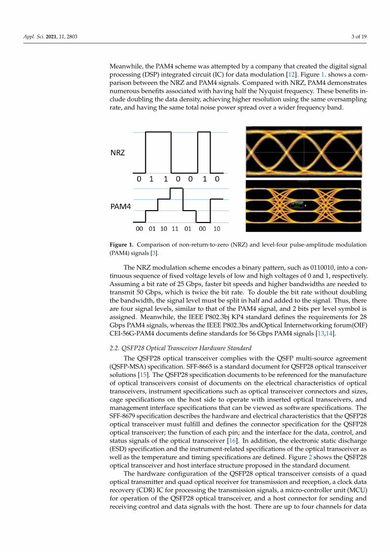
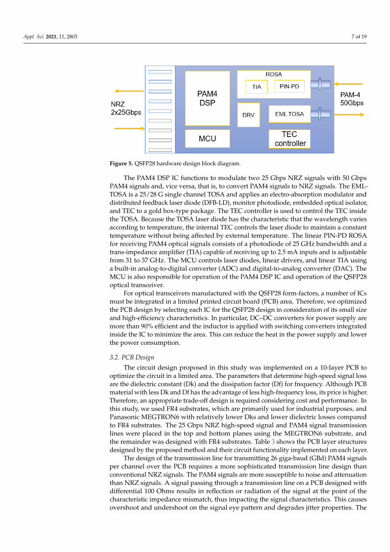
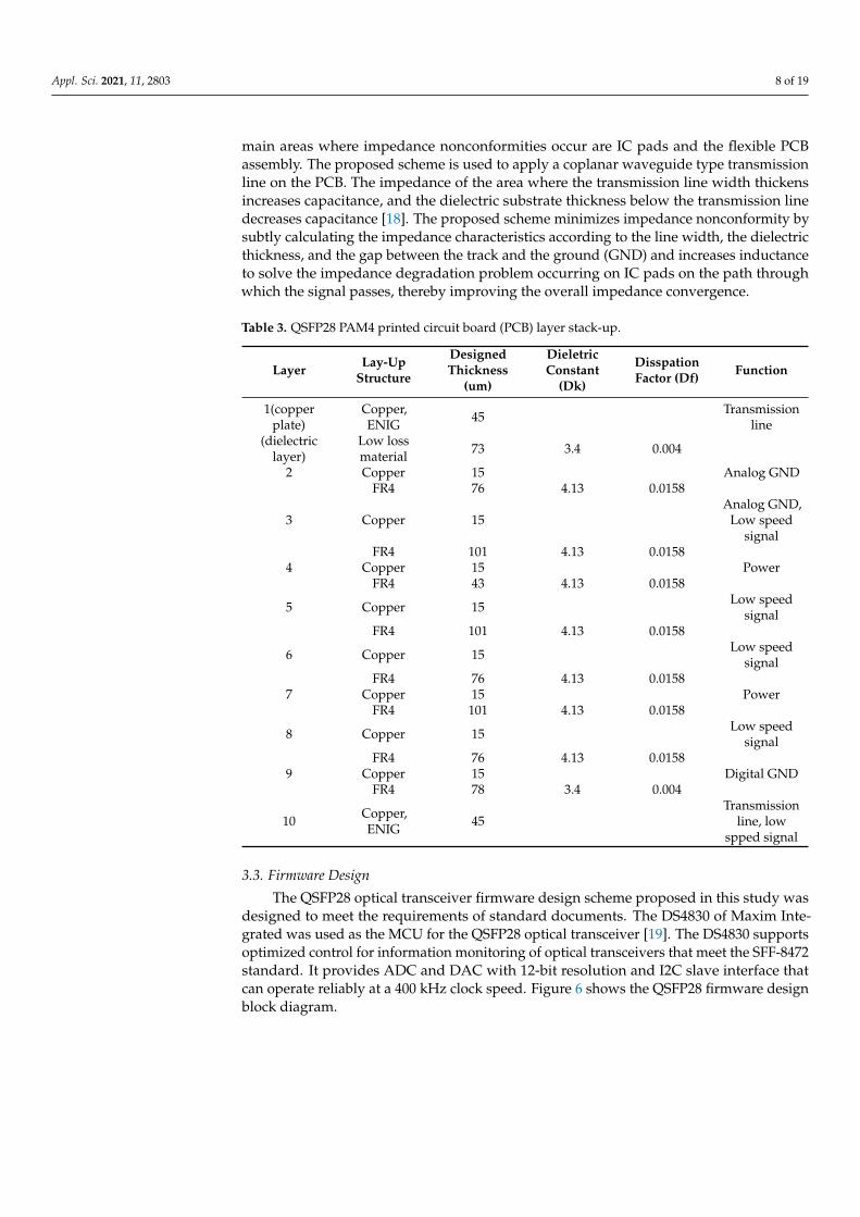
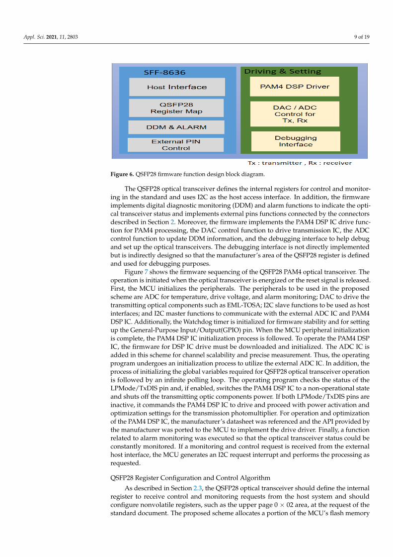
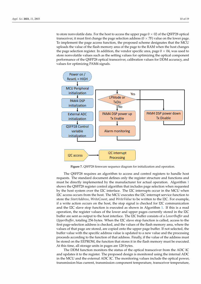
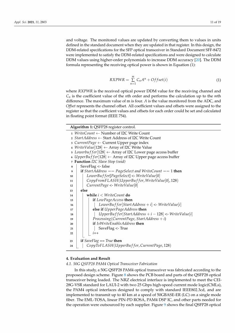
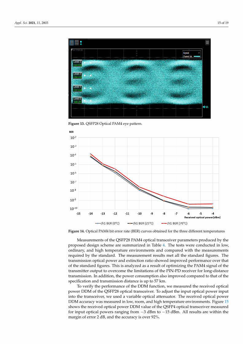
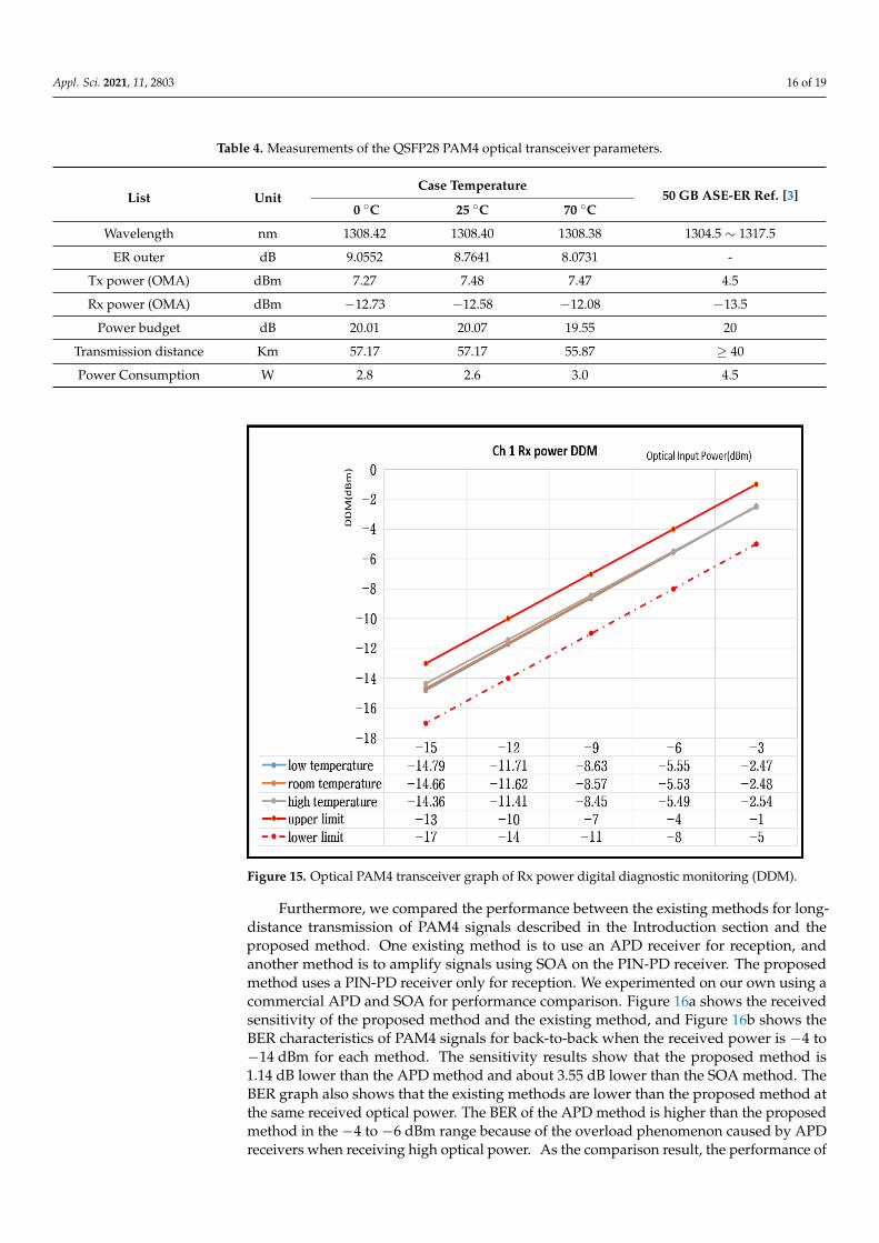
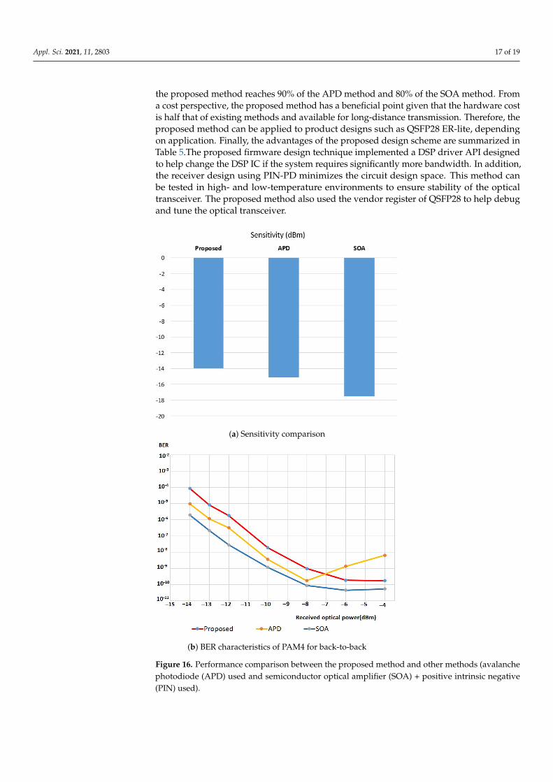
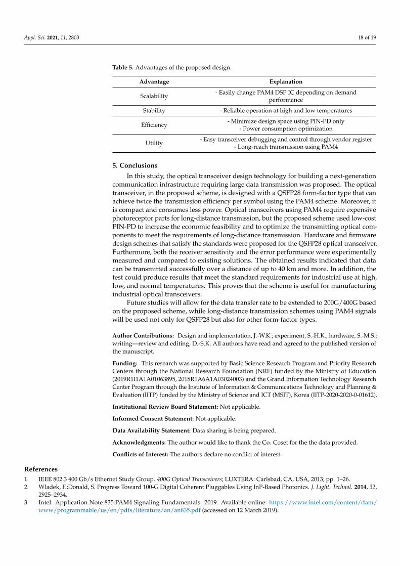
Copyright © 2022 FDOKUMEN