Reconfigurable Network Processor Implementation - DiVA Portal
59
Reconfigurable Network Processor Implementation GAZIZEH BABATAHERI Master of Science Thesis Stockholm, Sweden 2014 TRITA-ICT-EX-2014: 131
-
Upload
khangminh22 -
Category
Documents
-
view
0 -
download
0
Transcript of Reconfigurable Network Processor Implementation - DiVA Portal

Reconfigurable Network Processor Implementation
GAZIZEH BABATAHERI
Master of Science Thesis
Stockholm, Sweden 2014
TRITA-ICT-EX-2014: 131


Reconfigurable Network Processor
Implementation
Gazizeh Babataheri
Academic Examiner: Prof. Ahmed Hemani
Industrial Supervisor: Tume Wihamre
Master of Science
Stockholm 2014

2

i
Acknowledgments
I would like to thank the people at Ericsson AB, Digital ASIC Group to give me the chance
of performing my master thesis in that department. In particular I would like to thank my
supervisor Tume Wihamre for his perfect guidance and support.
Moreover, I want to thank my examiner at KTH, Professor Ahmed Hemani, for his guidance
during my thesis and entire my master studies.
Also, I would like to thank my mother, Amineh Moeini, and my sister, Sheller Babataheri,
for their understanding and support during my master studies.

ii
Abstract
Since most protocols use a limited set of basic functions to define the protocol, the feasibility
of runtime reconfigurable network protocol processor is studied in this thesis for next
generation of Ericsson’s EMCAs (Ericsson Multi Core Architecture).
For this purpose, common blocks between two protocols of 10G Ethernet and CPRI4.2 was
implemented in RTL level. For block level reconfigurability, generic function blocks are
implemented in SystemVerilog, tested in ModelSim and synthesized in Synopsys 28nm
technology. To achieve system level reconfigurability, muxing structure is used for blocks
communications with an enable controller function.
The results presented in this work, confirm that it is possible to implement a runtime
reconfigurable protocol processor in RTL level.
This work was performed at Ericsson AB, Digital ASIC Group at Kista, Stockholm, Sweden
during the time period of September 2013 to May 2014.

iii
Table of Contents
1 Introduction ............................................................................................................................ 1
1-1 Background ...................................................................................................................... 1
1-2 Problem Description ......................................................................................................... 1
1-3 Related Work .................................................................................................................... 2
1-4 Study Area ........................................................................................................................ 2
1-5 Method .............................................................................................................................. 3
1-6 Thesis Organization ......................................................................................................... 3
2 Background ............................................................................................................................. 4
2-1 OSI Model ......................................................................................................................... 4
2-2 Case Studies ..................................................................................................................... 5
2-2-1 10G Ethernet PCS/PMA type BASE-R ..................................................................... 5
2-2-1-1 10G Ethernet PCS/PMA type BASE-R Overview .............................................. 5
2-2-1-2 10G Ethernet PCS/PMA type BASE-R Functions ............................................. 6
2-2-2 CPRI4.2 ...................................................................................................................... 7
2-2-2-1 CPRI4.2 Overview ............................................................................................... 7
2-2-2-2 CPRI4.2 Functions .............................................................................................. 7
2-3 Common Functions of Case studies ................................................................................. 8
3 Flexible Common Blocks Implementation ............................................................................. 9
3-1 Control Word add/delete .................................................................................................. 9
3-1-1 Control Word add/delete Overview ........................................................................... 9
3-1-2 10GBASE_R Control Word add/delete .................................................................... 10
3-1-2 -1 10GBASE_R Control Word add/delete Functionality ..................................... 10
3-1-2 -2 10GBASE_R Control Word add/delete Implementation ................................. 12
3-1-3 CPRI4.2 Control Word add/delete ........................................................................... 14
3-1-3-1 CPRI4.2 Control Word add/delete Functionality ............................................. 14
3-1-3-2 CPRI4.2 Control Word add/delete Synchronization ......................................... 14
3-1-3-3 CPRI4.2 Control Word add/delete Implementation ......................................... 15

iv
3-2 Scrambler/Descrambler .................................................................................................. 17
3-2-1 Scrambler/Descrambler Overview........................................................................... 17
3-2-2 Scrambler Types ...................................................................................................... 18
3-2-2 -1 Synchronous (Additive) Scrambler/Descrambler Functionality ..................... 18
3-2-2 -2 Self-synchronizing (Multiplicative) Scrambler/Descrambler Functionality ... 18
3-2-3 Scrambler/Descrambler Implementation ................................................................ 18
3-3 Encoder/Decoder ............................................................................................................. 22
3-3-1 Encoder/Decoder Overview ...................................................................................... 22
3-3-1-1 What are the encoder and decoder? .................................................................. 22
3-3-1-2 Why encoder and decoder are used? ................................................................. 22
3-3-2 64b/66b Encoder/Decoder ........................................................................................ 22
3-3-2-1 64b/66b Encoder/Decoder Overview ................................................................. 22
3-3-2-2 64b/66b Encoder/Decoder Functionality ........................................................... 23
3-3-2-3 64b/66b Encoder/Decoder Implementation ...................................................... 24
3-3-3 8b/10b Encoder/Decoder .......................................................................................... 25
3-3-3-1 8b/10b Encoder/Decoder Overview ................................................................... 25
3-3-3-2 8b/10b Encoder/Decoder Functionality ............................................................. 25
3-3-3-3 8b/10b Encoder/Decoder Implementation ........................................................ 26
3-4 Gearbox ........................................................................................................................... 28
3-4-1 Gearbox Overview and functionality ...................................................................... 28
3-4-2 Gearbox Implementation ......................................................................................... 28
4 System Implementation ........................................................................................................ 31
4-1 Transmitter Block .......................................................................................................... 31
4-2 Receiver Block ................................................................................................................ 33
4-3 Model Application........................................................................................................... 35
4-3-1 xIO-s ......................................................................................................................... 35
4-3-2 CPRI6.0 .................................................................................................................... 36
4-3-3 1G/2G/4G Fibre Channel ......................................................................................... 37
4-3-4 Model Application Summery ................................................................................... 38
5 Results ................................................................................................................................... 39
5-1 Simulation Result ........................................................................................................... 39
5-1-1 10G Ethernet Simulation Result ............................................................................. 39

v
5-1-2 CPRI4.2 Simulation Result ..................................................................................... 40
5-2 Synthesis Result ............................................................................................................. 40
6 Conclusions and Future Work .............................................................................................. 42
6-1 Conclusions ..................................................................................................................... 42
6-2 Recommendations .......................................................................................................... 43
6-3 Future Work ................................................................................................................... 44
References ................................................................................................................................ 45

vi
List of Figures
Figure 1:Reconfigurable micro NPU SystemC model in transmission side (Figure 10 of [1]). 2
Figure 2: OSI Model Layers [2] and the focus area of this thesis. ............................................ 4
Figure 3: OSI Layer Model and IEEE802.3 Layer Model relationship (Adopted from figure
49-1 of [3]). ................................................................................................................................. 5
Figure 4: 10G BASE-R transmit functions. ............................................................................... 6
Figure 5: 10G BASE-R receive functions. ................................................................................. 6
Figure 6: CPRI interface (Adapted from figure 1 of [5]). .......................................................... 7
Figure 7: IEEE802.3 Layer Model (adopted from figure 6-1 of [3]). ....................................... 10
Figure 8: XGMII data stream. ................................................................................................. 10
Figure 9: Provide Start control character on the transmission side. ...................................... 11
Figure 10: Example of 8 control bits allocation for 64 data bits. ............................................ 11
Figure 11: 10GBASE_R transmitter and receiver blocks. ...................................................... 12
Figure 12: 10GBASE_R Control Word add/delete timing diagram. ....................................... 13
Figure 13:Represents Z.0.0 for 2457.6[Mbit/s] with the word width of 4 octets..................... 15
Figure 14: CPRI Control Word add/delete blocks diagram. .................................................... 15
Figure 15: Transmission FSM of CPRI module. ..................................................................... 16
Figure 16: Reception FSM of CPRI module............................................................................. 16
Figure 17: CPRI timing diagram. ............................................................................................ 16
Figure 18: 10GBASE_R Scrambler (Adapted from Figure 49-8 of [3]). .................................. 19
Figure 19: 10GBASE_R Descrambler (Adapted from Figure 49-10 of [3]). ............................ 19
Figure 20: CPRI4.2 Scrambler/Descrambler (Adapted from Figure 40 of [5]). ...................... 20
Figure 21: Scrambler/Descrambler block diagram. ................................................................ 20
Figure 22: Scrambler/Descrambler timing diagram. .............................................................. 21
Figure 23: 64b/66b Encoder/Decoder blocks diagram. ............................................................ 24
Figure 24: Encoder/decoder timing diagram. .......................................................................... 25
Figure 25: 5b/6b and 3b/4b encoding blocks. ........................................................................... 26
Figure 26: 8b/10b Encoder/Decoder block diagram. ................................................................ 27
Figure 27: 8b/10b Encoder/Decoder timing diagram. ............................................................. 27
Figure 28: Gearbox functionality. X1, X2 are data width and F1, F2 are data frequencies. . 28
Figure 29: Circular buffer for Gearbox implementation (In this figure, wr_ptr represents
write pointer and rd_ptr represents read pointer). ................................................................. 29
Figure 30: Gearbox block diagram. ......................................................................................... 30
Figure 31: tx_Gearbox/rx_gearbox timing diagram. .............................................................. 30
Figure 32: Transmitter block diagram. ................................................................................... 32
Figure 33: Receiver Block. ....................................................................................................... 33
Figure 34: Common blocks of xIO-s with CPRI4.2 in transmission side (10G Ethernet blocks
are shown with green color, CPRI4.2 blocks are shown with orange color and the xIO-s
blocks are shown in blue color). ............................................................................................... 35

vii
Figure 35: Common blocks of CPRI6.0 with CPRI4.2 and 10G Ethernet in transmission side
(10G Ethernet blocks are shown with green color,CPRI4.2 blocks are shown with orange
color and the CPRI6.0 blocks are shown in purple color). ...................................................... 36
Figure 36: Common blocks among 1/2/4Gbps Fibre Channel and CPRI4.2 in transmission
side (10G Ethernet blocks are shown with green color, CPRI4.2 blocks are shown with
orange color and the 1/2/4G Fibre channel blocks are shown in grey color). ......................... 37
Figure 37: Common blocks among 10G Ethernet,CPRI4.2, xIO-s, CPRI6.0, 1/2/4Gbps Fibre
Channel in transmission side (10G Ethernet blocks are in green color, CPRI4.2 blocks are in
orange color, xIO-s blocks are in blue color,CPRI6.0 blocks are in purple and the 1/2/4G
Fibre channel blocks are shown in grey color). ....................................................................... 38
Figure 38: 10G Ethernet test case simulation. ....................................................................... 39
Figure 39: CPRI4.2 test case simulation. ................................................................................ 40

viii
List of Tables
Table 1: 10GBASE_R transmitter FSM description. .............................................................. 12
Table 2: Reception FSM description (“P” represents one octet of Preamble: 10101010 and
“SFD” represents Start Frame Delimiter: 10101011). ............................................................ 13
Table 3: Length of control word (Adapted from table 3 of the reference [5]). ......................... 14
Table 4: 64b/66b encoding look up table (Adapted from Figure 49-7 of [2]). .......................... 24
Table 5: Synthesis Results. ...................................................................................................... 41

ix
List of Abbreviations
CRC Cyclic Redundancy Check
PRBS Pseudo-Random Binary Sequence
FIFO Fist In,First Out
ASIC Application Specific Integrated circuit
10G Ethernet 10Gitabit Ethernet
CPRI4.2 Common Public Radio Interface version 4.2
TLM Transaction Level Modeling
RTL Register Transistor Level
NPU Network Processor Unit
OSI Open System Interconnection model
XGMII 10 Gigabit Media Independent Interface
MDI Medium Dependent Interface
PCS Physical Coding Sublayer
PMA Physical Medium Attachment
MAC Media Access Control
REC Radio Equipment Control
RS Reconciliation Sublayer
BF Basic Frame
HF Hyper Frame
RF Radio Frame
LFSR Linear Feedback Shift Register
PLL Phase Locked Loop

1
1 Introduction
1-1 Background
For communication between different nodes in a network, data should be exchanged with a
standard structure. Protocols define the data exchange rules via a set of instructions. There
are different protocols for different applications and different systems. Some of them are
open source and some of them are proprietary [1].
Most protocols use a limited set of basic functions to define the protocol and the interactions
in it. These functions manipulate data in a transmission side in order to perform to reliable
data transfer. Original data is recovered in the reception side by doing opposite functions.
The most common functions are [1]:
CRC calculate and check
Scrambling and descrambling
Coding and Decoding
Framer and Deframer
PRBS and loopback capability
Gearbox
Striping and aligning
Queues and FIFOs
Protocol State machine
Fragmentation and Defragmentation
Retransmit
Checksum
Surveillance registers and counters
1-2 Problem Description Ericsson AB uses hard-wired communication protocols in its today ASICs which are:
Not flexible for different protocols
Not flexible for different products in one protocol family. For example it is not
flexible for 10G Ethernet and 2.5G Ethernet.
Not flexible for different bit rate per lane.
Not flexible for different amount of interface lanes (total bandwidth).

2
Moreover, it is costly for Ericsson AB to define new protocols for a new product in terms of
man-years and lead-time.
Furthermore, the hardware function overlap between different protocols is costly in terms of
area and power.
Since most of the protocols are very similar in the functionality, reconfigurable protocol
processor is desired.
1-3 Related Work This study is the continuation of previous master thesis at Ericsson AB. Sara Karlsson
investigated that it is possible to design and implement a reconfigurable micro Network
Processor Unit using SystemC/TLM2.0. The SystemC model is reconfigurable for 10G
Ethernet and xIO-s based on the configuration file [1].Figure1 shows that based on the
protocol of choice, configuration file set the data transmission functions.
Figure 1: Reconfigurable micro NPU SystemC model in transmission side (Figure 10 of [1]).
1-4 Study Area This work studies the feasibility of architecting and implementing a runtime reconfigurable
network protocol processor in RTL level.

3
1-5 Method To investigate the feasibility of the runtime reconfigurable network protocol processor in
RTL level, 10G Ethernet and CPRI4.2 protocols were proposed to study by Ericsson AB. The
flow of investigation was as follow:
The case studies specifications are studied to find the focused area functions.
Common functions between two case studies were found.
Architecture of the reconfigurable network protocol processor transmitter and
receiver were designed.
The common functions were implemented in RTL. Common functions were
implemented with the parameterized SystemVerilog blocks to achieve block level
flexibility.
Every function block in transmission side and its opposite function in reception side
were tested and simulated in ModelSim to ensure that data is recovered correctly.
To allow functional blocks to be connected in different orders, which is flexibility
required supporting different protocols, muxing structure is used.
The transmitter and receiver blocks were implemented in SystemVerilog and
controlled by an enable controller to start data processing in correct time.
The transmitter and receiver blocks were connected to each other and tested in
ModelSim with different test cases for both case study protocols.
1-6 Thesis Organization This thesis divided into 6 chapters.
Chapter 1 contains the background of this work, identifying the problem, what others have
done, what this study is focused on and the used method for solving the problem.
Chapter 2 contains the overview of the case studies for this work and finding the common
functions between two case uses.
Chapter 3 is the result of literature study for this work and applying knowledge into
practice for block level implementation.
Chapter 4 is explained the system level implementation and model application.
Chapter 5 shows the result of this work presented in simulation wave forms and synthesis
figures.
Finally, chapter 6 presents the conclusion of this study and recommendations for the
industry and for future area of interest.

4
2 Background
2-1 Model Open Systems Interconnection model (OSI) partitions a communication system into 7
abstraction layers to standardize the internal functions [2]. Figure 2.1 shows the 7 layers of
OSI model.
Figure 2: OSI Model Layers [2] and the focus area of this thesis.
Application Layer provides applications to access network services.
Presentation Layer provides the format which is understandable for the application layer.
Session Layer provides session connections between different stations.
Transport Layer provides the reliable way of data transportation.
Network Layer provides the network path to transmit/receive data.
Data Link Layer provides error-free data transmission/reception over physical layer.
Physical Layer provides the hardware means of data transmission/reception.
This study focuses on physical layer.
7.Application
6.Presentation
5.Session
4.Transport
3.Network
2.Data Link
1.Physical

5
2-2 Case Studies According to the thesis requirements, two protocols are studied in this work:
10G Ethernet PCS/PMA type BASE-R
CPRI4.2
2-2-1 10G Ethernet PCS/PMA type BASE-R
2-2-1-1 10G Ethernet PCS/PMA type BASE-R Overview IEEE 802.3 standard is described the Ethernet protocol which is an open protocol for data
communication over a solid medium [3].Figure 2.2 depicts the relationship between OSI
Model and IEEE802.3 Layer Model type BASR-R[3].
Figure 3: OSI Layer Model and IEEE802.3 Layer Model relationship (Adopted from figure 49-1 of
[3]).
Layer 2 (Data Link Layer) has two sublayers [4].
Logic Link Control is responsible for identifying network layer protocol.
Media Access Control is responsible for data packet format.
Layer 1 (Physical Layer) has its own sublayers [4].
7.Application
6.Presentation
5.Session
4.Transport
3.Network
2.Data Link
1.Physical
Logic Link Control
Media Access Control
Reconciliation Sublayer
XG
MII
Physical Coding Sublayer
Physical Medium Attachment
Physical Medium Dependent
MD
I
Medium

6
Reconciliation Sublayer is responsible for signal mapping between MAC (Media
Access Control) and XGMII(10 Gigabit Media Independent Interface).
Physical Coding Sublayer is responsible for coding and encoding data stream.
Physical Medium Attachment is responsible for serializing and synchronization.
Physical Medium Dependent is responsible for signal transmission/reception to/from
Medium.
This study focuses on PCS(Physical Coding Sublayer).
2-2-1-2 10G Ethernet PCS/PMA type BASE-R Functions
Figure 2.3 shows the PCS transmit functions and figure 2.4 shows the PCS receive functions
of 10 G Ethernet BASE-R type. The functions are explained in chapter 3.
Figure 4: 10G BASE-R transmit functions.
Figure 5: 10G BASE-R receive functions.
Control word
add 64b/66b Encoder
Scrambler
G(x)=1+x39+x58
66b/16b
Gearbox
Control word delete
66b/64b Decoder Descrambler
G(x)=1+x39+x58
16b/66b
Gearbox

7
2-2-2 CPRI4.2
2-2-2-1 CPRI4.2 Overview Common Public Radio Interface (CPRI) is an open standard interface between the Radio
Equipment Control (REC) and the Radio Equipment (RE) in a wireless base station. CPRI
specification is the industrial cooperation of five leading base station hardware companies:
Ericsson AB, Huawei Technologies Co. Ltd., NEC Corporation, Nortel Networks and
Siemens AG [5].
Figure 6: CPRI interface (Adapted from figure 1 of [5]).
The REC(Radio Equipment Control) contains digital baseband radio functions and RE
(Radio Equipment) provides analogue radio frequency functions.
Downlink is the data stream from REC to RE.
Uplink is the data stream from RE to REC.
2-2-2-2 CPRI4.2 Functions
REC functions are investigated because it concerns about network interface and digital
signals which is related to this work. Some of the REC functions are:
Downlink functions: Channel Coding, Interleaving, Spreading, Scrambling,…
Uplink functions: channel Decoding, Deinterleaving, Despreading, Descrambling,…
Radio Equipment Control
Layer 2
Layer 1
Radio Equipment
Layer 2
Layer 1
CPRI
Radio Base Station System
Network Interface Air Interface
CPRI Interface

8
2-3 Common Functions of Case studies The common functions between 10G Ethernet PCS type10BASE-R and CPRI4.2 REC are
Scrambling/Descrambling, Encoding/Decoding.
For both protocols, Control Words should be added in the transition side and deleted in the
reception side in order to provide the data boundary .Moreover, there should be gearboxing
function in both transmission and reception side to convert one data width to another data
width in order to provide output bit width.
Therefore four common blocks between two case study protocols are selected to be
implement in this work. The common functions are:
• Control Word add/delete
• Scrambling/Descrambling
• Encoding/Decoding
• Gearboxing

9
3 Flexible Common Blocks
Implementation
In this section, the functionality of the common blocks is described and the flexible
implementation of them is explained. The subsections are as follows:
Control Word add/delete
o 10G Ethernet Control Word add/delete
o CPRI4.2 Control Word add/delete
Scrambler/Descrambler
o Synchronous Scrambler/Descrambler
o Self-synchronizing Scrambler/Descrambler
Encoder/Decoder
o 64b/66b Encoder/Decoder
o 8b/10b Encoder/Decoder
Gearbox
3-1 Control Word add/delete
3-1-1 Control Word add/delete Overview In packet based protocols like 10G Ethernet, data is transmitted in the form of packets. For
accurate data transmission, the boundary of the packets should be recognized. For this
purpose, control words are added to data in the transmission side and they will be deleted in
the reception side in order to recover data.
In stream serial based protocols like CPRI4.2, data is put in packages in order to let the
receiver get information on the data format [6]. For this purpose, Control words are added
in transmission side and they are deleted in reception side. Moreover, CPRI4.2 use control
words for layer 1 synchronizations [5].

10
3-1-2 10GBASE_R Control Word add/delete
3-1-2 -1 10GBASE_R Control Word add/delete Functionality XGMII is the standard interconnection between Reconciliation Sublayer (RS) and the
Physical Coding Sublayer (PCS) for 10 Gb/s operation [3].
Figure 7: IEEE802.3 Layer Model (adopted from figure 6-1 of [3]).
Data packets transmitted through XGMII should fulfil XGMII data stream structure [3]
shown in figure 3.2.
IFG(12 octets) Preamble
(7 octets)
SFD
(1 octet) Data(46-1500 octets) EFD(1 octet)
Figure 8: XGMII data stream.
The figure 3.2 contents are described as below based on [3].
IFG(Inter Frame Gap)
The Inter Frame Gap is the period on which no data activity occurs on the XGMII
interface and it is specified as minimum 12 octets of “Idle” character (0x07).
Preamble
Frame transmission begins with the 7 octets sequence as below
10101010 10101010 10101010 10101010 10101010 10101010 10101010
SFD(Start Frame Delimiter)
SFD indicates the start of a frame. It is transmitted after preamble with the value of:
10101011
Data
It consists of data octets.

11
EFD(End of Frame Delimiter)
EFD indicates the frame termination and defined as/T/, Terminate control character
and the value of 0xfd.
On the transmission side, RS converts the first octet of preamble to the Start character
(0xfb) to be recognized by PCS as the start of frame data. First preamble is valid if it
transmitted in octet 0 or octet 4 [3].Figure 3.3 shows the first preamble conversion to the
start control character in the transmission side.
10101010 10101010 10101010 10101010 10101010 10101010 10101010 10101011
11111011 10101010 10101010 10101010 10101010 10101010 10101010 10101011
Figure 9: Provide Start control character on the transmission side.
On the reception side, RS converts the Start control character to the “10101010” in order to
convert data format to the XGMII data stream.
For each 64 bits input block in transmission side, there is a block of 8 bits control output to
detect the pure data octets from control character octets. If transmitting octet is pure data
the corresponding control bit is "0” and if the data octet is a control character, the control bit
is “1”[3] .Figure 3.4 shows an example of control bits allocation for a 8 octet data stream.
Figure 10: Example of 8 control bits allocation for 64 data bits.
MSB
8 data
octets Idle Terminate Data Data Data Data Data Data
8control
bits 1 1 0 0 0 0 0 0

12
3-1-2 -2 10GBASE_R Control Word add/delete Implementation
Figure 3.5 shows the block diagram of 10GBASE_R transmission and reception blocks.
Figure 11: 10GBASE_R transmitter and receiver blocks.
To detect packet boundary, tx_XGMII_if and rx_XGMII_if blocks are implemented with two
finite state machines. For improper sequences of data, Error (E= 0xfe) character is provided.
Table 3.1, table 3.2 describe the two mentioned state machines respectively.
Table 1: 10GBASE_R transmitter FSM description.
current
state input
next
state output
Idle
8 Idle octets are received Idle dout ==din
ctrl_out=={8'b11111111}
7 preambles and one SFD are received Data dout =={SFD,P,P,P,P,P,P,S}
ctrl_out =={8'b00000001}
preamble in octet 4 is received P4 dout == {P,P,P,S,I,I,I,I})
ctrl_out =={8'b00011111}
others Idle dout == {E,E,E,E,E,E,E,E}
ctrl_out =={8'b11111111}
P4
preambles in octets 5,6,7 and SFD in
octet 7 are received Data
dout ==din
ctrl_out =={8'b00000000}
others Idle dout == {E,E,E,E,E,E,E,E}
ctrl_out =={8'b11111111}
Data
Error character is received Idle
dout == din
ctrl_out :control bit of Error
octet is assigned to 1
Terminate character is received Idle
dout ==din
ctrl_out :control bit of Terminate
octet is assigned to 1
others Data dout ==din
ctrl_out =={8'b00000000}

13
Table 2: Reception FSM description (“P” represents one octet of Preamble: 10101010 and “SFD”
represents Start Frame Delimiter: 10101011).
In order to test 10GBASE_R Control Word add/delete blocks, they are connected and tested
in different cases.
Timing diagram of 10GBASE_R Control Word add/delete blocks for two test cases is shown
in figure 3.6. Figure 3.6 shows two different bit sequences. The first test case which is
transmitted from tick 2 to tick 17, describes sending a correct bit sequences. The second test
case which is started in tick 17 shows an erroneous bit sequence with sending preamble in
wrong octet (octet 5).
Figure 12: 10GBASE_R Control Word add/delete timing diagram.
current
state input next state output
Idle
8 Idle octets are received Idle dout ==din
Start character and 7 preambles are received Data Dout=={SFD,P,P,P,P,P,P,P}
Start in octet 4 is received S4 dout == {P,P,P,P,I,I,I,I}
Others Idle dout ={E,E,E,E,E,E,E,E}
S4
preambles in octets 5,6,7 and SFD in octet 7
are received Data dout ==din
Others Idle dout=={E,E,E,E,E,E,E,E}
Data
Error character is received Idle dout=={E,E,E,E,E,E,E,E}
Terminate character is received Idle dout ==din
Others Data dout ==din

14
3-1-3 CPRI4.2 Control Word add/delete
3-1-3-1 CPRI4.2 Control Word add/delete Functionality CPRI4.2 specification [5] includes Layers 1 and 2 of the OSI model. Data frame format in
layer 2 shall follow MAC frame structure. To organize data in serial stream, data bits are
combined in packages in layer 1. The smallest package which is called Basic Frame (BF)
consists of 16 words with the indexes of W0…W15.
The word length depends on the line bit rates which are provided in CPRI4.2 layer 1
specification [5]. Table 3.3 shows the word length for different bit rates.
CPRI line bit
rate[Mbit/s] word length[bit]
614.4 T=8
1228.8 T=16
2457.6 T=32
3072.0 T=40
4915.2 T=64
6144.0 T=80
9830.4 T=128
Table 3: Length of control word (Adapted from table 3 of the reference [5]).
256 Basic Frame are packed in a bigger set which is called Hyper Frame (HF).150 of the HF
are combined in an even bigger package called Radio Frame(RF) which provide 10 ms used
for synchronizing the Radio Base Station network. Z.X.W.Y is introduced by CPRI4.2
specification to identify data.
Z: represents the number of hyper frame.
X: represents the number of basic frame.
W: represents the number of word in a basic frame.
Y: represents the number of byte in a word
For example: 0.46.5.7 means that byte 7 of word 5 in the 46th basic frame of first hyper
frame.
3-1-3-2 CPRI4.2 Control Word add/delete Synchronization There are some control words in CPRI4.2 specification in order to synchronize data frames.
More information about the control characters are available via table 8 and table 9 of [5].
In this study, just the control character for start of Hyper Frame is applied .Every Hyper
Frame is marked out with a special code K28.5 which is located in word 0 of basic frame
0(Z.0.0).As the word width is vary between different line bit rates and K28.5 is just one octet
(“8’b10111100”), remained bits of the word width is assumed as zero. Figure 3.7 shows the
applied control word in this study for bit rate of 2457.6[Mbit/s] as an example.

15
Figure 13: Represents Z.0.0 for 2457.6[Mbit/s] with the word width of 4 octets.
3-1-3-3 CPRI4.2 Control Word add/delete Implementation
Figure 3.8 shows blocks diagram of CPRI Control Word add/delete modules for transmission
and reception sides.
Figure 14: CPRI Control Word add/delete blocks diagram.
The bpw input port is allocated for line bit rate configuration. CPRI Control Word
add/delete modules are implemented by finite state machines and counting cycles in order
to assert control character to the right position. For this purpose, data is buffered into a
FIFO and it is retrieved after control word assertion. Applying accurate write pointer and
read pointer values are necessary to avoid data corruption. Figure 3.9 shows the concept of
CPRI transmission state machine. FSM looks for start of the hyper frames by counting clock
cycles, when start of each hyper frame is found control words is added to the data stream.
K28.5
0
DATA
0
0
W0 W1-W15

16
For example, if the line bit rate of 6144.0 [Mbit/s] is configured, FSM assert control words
into data stream in every 5120 coming cycles.
Number of bits in each word for 6144.0 [Mbit/s] line bit rate: 80bits
Number of bits in a Basic Frame: 16 *80=1280 bits
One Basic Frame is transmitted in ((1280bits/64bits) =20) cycle.
One Hyper Frame is transmitted in (256*20=5120) cycles
For line bit rate of 6144.0 Hyper Frames is founded in every multiple of 5120 cycles.
Figure 15: Transmission FSM of CPRI module.
In reception side, a finite state machine, Searches for control words and delete them in
order to align data and recover it. Figure 3.10 shows the FSM in the reception side.
Figure 16: Reception FSM of CPRI module.
Two modules for CPRI control word add in transmitting and CPRI control word delete in
receiving sides are connected to each other to test all line bit rates. Figure 3.11 shows the
test case for line bite rate of 6144.0 [Mbit/s]. As can be seen in the figure 3.11 data is
recovered after some cycles.
Figure 17: CPRI timing diagram.

17
3-2 Scrambler/Descrambler
3-2-1 Scrambler/Descrambler Overview 3-2-1-1 What are the scrambler and descrambler?
Scrambler which is also known as randomizer manipulates data before transmitting in the
transmission side .The manipulated data will be unscrambled on the receiving side by the
descrambler. Scrambling is based on Pseudo-Random Binary Sequence (PRBS) generated by
Linear Shift Registers (LFSR) and modulo-2-addition functions [7]. PRBS is applying to the
input data to continuously generate random outputs. Scrambling is described with
polynomial of “1+Xm+Xn” format in which “m” and “n” describe shift register numbers which
should be operated and “+” is the xor operator [8].
3-2-1-2 Why scrambler and descrambler are used?
The main reason of using scrambler and descrambler is reducing the probability of
occurring long length of zeroes and ones by randomizing data.
In order to ensure that adequate data is decoded in the receiving side following factors
should be considered before transmitting data in the transmission side. Scrambling data
helps to improve these factors.
Transition density: In serial data stream, transition density is defined as the ratio of
edges to the total number of unit intervals[9].For recovering accurate representation
of transmit clock at the receiving side, adequate transition density is required for
PLL(Phase Locked Loop) to extract timing information. With the long length of
zeroes and ones, the clock recovery circuitry tends to drift in the receiver side
because of phenomena called baseline wandering. For data value determination,
receiver calculates the average of incoming signal power which is named baseline.
Long length of zeroes and ones make a drift in the baseline and baseline wandering
occurs [10].
DC balance: DC balance means the equality in the number of ones and zeroes over
unit intervals [11]. When data contains the long numbers of zeroes and ones the
voltage level in a digital signal will be constant for a while and the spectrum creates
very low frequency. For some transmission mediums which cannot pass low
frequencies, data should be DC balanced before transmitting [10].

18
3-2-2 Scrambler Types
synchronous scrambler
self-synchronizing scrambler[8].
3-2-2 -1 Synchronous (Additive) Scrambler/Descrambler Functionality This type of scrambler generates a cyclical sequence of PRBS with a particular initial state
called sync-word which used for synchronization. Synchronous descrambler is the same
module as the synchronous scrambler [12].
The advantage of using this type of scrambler is that there is one bit error per transmission
error and the disadvantage is that Scrambler/Descrambler should be synchronized [14].
3-2-2 -2 Self-synchronizing (Multiplicative) Scrambler/Descrambler
Functionality This type of scrambler is the modification of synchronous type. The transmitted/received
data is used as the input to the LFSR state. In other words, there is no need of sync-word
for synchronization and that is why they are called self-synchronizing scramblers. The
output from the scrambler is copied into a shift register so the scrambler contains a copy of
the previous bits [12].
The descrambler module is very similar to the scrambler one. The only difference is that
input is copied to the shift register rather than output as for the scrambler [8].
The positive point of using self-synchronizing scrambler is that there is no need for sync-
word and the negative point is there are minimum three error bits per transmission error
[14].
3-2-3 Scrambler/Descrambler Implementation According to IEEE.3ae, Physical Coding Sublayer (PCS) type 10GBASE-R use the self-
synchronizing scrambler with polynomial G(x)= 1+X39+X58 [3].
Figure 3.12 show scrambler and figure 3.13 shows descrambler used in type 10GBASE-R
respectively.

19
Figure 18: 10GBASE_R Scrambler (Adapted from Figure 49-8 of [3]).
Figure 19: 10GBASE_R Descrambler (Adapted from Figure 49-10 of [3]).
Synchronous Scrambler is used for CPRI protocol with the polynomial of G(x)=
1+X28+X31.Scrambler is synchronized with Sync-word through each Hyper Frame.Figure
3.14 shows scrambler and descrambler functionality of CPRI protocol [5].

20
Figure 20: CPRI4.2 Scrambler/Descrambler (Adapted from Figure 40 of [5]).
The scrambler and descrambler modules for both types have the same block diagram with 5
inputs and 1 output. Figure 3.15 shows scrambler and descrambler blocks. Generic
Polynomial of “G(x) =1+Xn+Xm” is implemented via TAP_L and TAP_S inputs. TAP_L is
designed for specifying large tap polynomial and TAP_S is designed for implementation of
small tap polynomial. In this work maximum size of tap polynomials are considered as 64.
This size covers the scrambler’s polynomials of case studies as well as protocols mentioned
in section 4-3.
Data input and data output are generic in width and the maximum data width is set to 128
bits.
Figure 21: Scrambler/Descrambler block diagram.

21
Figure 3.16 shows the timing diagram of testing Scrambler/Descrambler. Some test vectors
are applied to both scrambler types. Scrambled data is available after one clock cycle and
original data in recovered from descrambler after two clock cycles.
Figure 22: Scrambler/Descrambler timing diagram.

22
3-3 Encoder/Decoder
3-3-1 Encoder/Decoder Overview
3-3-1-1 What are the encoder and decoder? Encoding is the process which deals with transmitting data over physical layer in a way to
be recovered safer in the receiving side. Decoding is the opposite process in which original
data is recovered.
3-3-1-2 Why encoder and decoder are used? Following factors can be supported by the help of encoder in the transmission side [14].
Transition density: There should be sufficient transition density to recover the clock
at the receiver. The scrambler decrease the probability of long length of zeros and
ones but it doesn’t guarantee that never long length of zeros and ones occurs.
Encoder 8b/10b has a high transition density. Encoder 64b/66b is used when the high
overhead of encoder 8b/10b is not worth. In this case encoder 64b/66b improves
transition density with the help of scrambler.
DC-balance: Like for the scrambler also the encoder helps improving DC-balance.
Encoder 8b/10b is DC-balanced but encoder 64b/66b relies on scrambler for this
purpose.
Timing of bits: Control characters like start and end of the frame should be
recognized in the receiving side to decode data in the correct time.
Error detection: invalid codes should be detected before transmission.
Run-length: In serial data stream, the maximum continuous number of zeroes and
ones called maximum run length. The smaller maximum run-length value means
higher transmission density which helps the clock recovery. Encoder 8b/10b has the
maximum run-length of 5.The run-length of encoder 64b/66b is 66bits which will be
improved by the scrambler.
3-3-2 64b/66b Encoder/Decoder
3-3-2-1 64b/66b Encoder/Decoder Overview 64b/66b encoding/decoding is defined by IEEE 802.3ae which is used for PCS type
10GBASE-R due to its characteristics of low overhead and quick sync code. This encoder
relies on scrambler for run length, DC-balance and clock recovery [14].

23
3-3-2-2 64b/66b Encoder/Decoder Functionality
Encoder block receive 64 bits (8 octets) data word and 8 bits control word. Each bit of control
word represents the type of corresponding data octet. If the control bit is zero, the data octet
are pure data and if the control bit is one, the data octet contains the control character. For
instance, control word of “8b’00001111” shows that octet 0,1,2,3 are pure data and the last
forth octets are control characters.
Control characters are the ones sent from the MAC (XGMII Interface) to PCS as below:
/I/ indicates Idle octet with the value of 0x07.
/S/ indicates Start of frame with the value of 0xfb.
/T/ indicates end of frame with the value of 0xfd.
/E/ indicates Erroneous octets with the value of 0xfe.
/Q/ indicates sequence ordered set with the value of 0x9c.
66 encoded data contains 2 bits of sync word and 64 bits of data word.
Sync word is 2’b01 if the whole 64 receiving bits are pure data and it is 2’b10 if the 64
receiving data contains control characters.
In case, sync word is 2’b01, 64 bits of encoded data is the same as 64 input bits.
If sync word is 2’b10, 64 encoded data depends on the input data. In this case, the first octet
called type field to specify the type of input data. The remained 56 bits are the encoded data
in which input control octets encoded in to 7 bits control codes and data octets pass the
encoder. The 7 bits control code is:
Idle encoded as 0x00.
Start encoded by the type field.
Terminate encoded by the type field.
Error encoded as 0x1e.
Sequenced ordered set encoded by the type field and o-code which is 4’b0000.
Table 3.4 shows the inputs and encoded output of encoder block.
data input [63:0] control input output [65:10] output[1:0]
D7,D6,D5,D4,D3,D2,D1,D0 8'b00000000 D7,D6,D5,D4,D3,D2,D1,D0 2'b01
data input [63:0] control input [7:0] output[65:10] output[9:2] output[1:0]
I7,I6,I5,I4,I3,I2,I1,I0 8'b11111111 C7,C6,C5,C4,C3,C2,C1,C0 0x1e 2'b10
E7,E 6,E5,E4,E3,E2,E1,E0 8’b11111111 C7,C6,C5,C4,C3,C2,C1,C0 0x1e 2’b10
D7,D6,D5,S4,I3,I2,I1,I0 8'b00011111 D7,D6,D5,4'b0000,C3,C2,C1,C0 0x33 2'b10
D7,D6,D5,D4,D3,D2,D1,S0 8'b00000001 D7,D6,D5,D4,D3,D2,D1 0x78 2'b10
I7,I6,I5,I4,I3,I2,I1,T0 8'b11111111 C7,C6,C5,C4,C3,C2,C1,7'b0000000 0x87 2'b10
I7,I6,I5,I4,I3,I2,T1,D0 8'b11111110 C7,C6,C5,C4,C3,C2,6'b000000,D0 0x99 2'b10
I7,I6,I5,I4,I3,T2,D1,D0 8'b11111100 C7,C6,C5,C4,C3,5'b00000,D1,D0 0xaa 2'b10
I7,I6,I5,I4,T3,D2,D1,D0 8'b11111000 C7,C6,C5,C4,4'b0000,D2,D1,D0 0xb4 2'b10
I7,I6,I5,T4,D3,D2,D1,D0 8'b11110000 C7,C6,C5,3'b000,D3,D2,D1,D0 0xcc 2'b10
I7,I6,T5,D4,D3,D2,D1,D0 8'b11100000 C7,C6,2'b00,D4,D3,D2,D1,D0 0xd2 2'b10
I7,T6,D5,D4,D3,D2,D1,D0 8'b11000000 C7,1'b0,D5,D4,D3,D2,D1,D0 0xe1 2'b10
T7,D6,D5,D4,D3,D2,D1,D0 8'b10000000 D6,D5,D4,D3,D2,D1,D0 0xff 2'b10

24
Table 4: 64b/66b encoding look up table (Adapted from Figure 49-7 of [2]).
D7-D0 indicates the input data octets.C7-C0 indicates the encoded 7bits control codes
corresponding input control octets. In this study, control octets assumed as Idle
character. It is assumed there is one possibility of occurring Error character and it is
when all 64 input bits are Error characters.
3-3-2-3 64b/66b Encoder/Decoder Implementation
Figure 3.17 shows the block diagram of encoder 64b/66b and decoder 66b/64b.
Figure 23: 64b/66b Encoder/Decoder blocks diagram.
The functionality of encoder 64b/66b is described here. Decoder functionality is the reverse
functionality of encoder.
The module has 5 input ports which are 64 bits data input, 8 bits control input and 3 input
ports for clock, reset and enable. Encoder module operates the encoding operation on the
input data with the help of control bits to generate 64 output data with 2 bits for
synchronization. If the combination of data and control words is not valid, encoder send
erroneous bits with error information to the next module.
D7,D6,D5,Q4,I3,I2,I1,I0 8'b00011111 D7,D6,D5,4'b1111,C3,C2,C1,C0 0x2d 2'b10
I7,I6,I5,I4,D3,D2,D1,Q0 8'b11110001 C7,C6,C5,C4,D3,D2,D1,4'b1111 0x4b 2'b10
D7,D6,D5,Q4,D3,D2,D1,Q0 8'b00010001 D7,D6,D5,8'b11111111,D3,D2,D1 0x55 2'b10
D7,D6,D5,S4,D3,D2,D1,Q0 8'b00010001 D7,D6,D5,8'b00001111,D3,D2,D1 0x66 2'b10

25
Implementation of Encoder/Decoder 64b/66b is based on the IEEE 802.3ae standard, clause
49[2]. They are implemented with two look up tables in this study. Encoder and decoder are
connected to each other for testing different combination of data inputs according table 3.4.
The timing diagram of Encoder/Decoder 64b/66b is shown in figure 3.18. Two test case
examples are represented in the figure 3.18. In the first case, after one 64 bits block of Idles
the Start character is transmitted following by some Data octets and the Terminate
character. Second test case shows testing the invalid block. Start character is sending in
wrong octet (start character should be transmitted in octet 0 or octet 4 [2]). After one clock
cycle encoded data is available with information of sync-word, type field and data field. The
encoded data decodes by decoder one clock cycle later and the original data is recovered with
2 clock cycle latency.
Figure 24: Encoder/decoder timing diagram.
3-3-3 8b/10b Encoder/Decoder
3-3-3-1 8b/10b Encoder/Decoder Overview
According CPRI Specification, V4.2 the MAC frame is encoded by 8b/10b encoder [5].
The 8b/10b Encoding/Decoding standard could be the choice for other high speed serial
communication standards due to its characteristics of maximum run-length, DC balanced
data stream and clock recovery because of the Running Disparity.
In this section, the functionality of encoder 8b/10b is briefly explaned.8b/10b encoding was
invented by Albert X. Widmer and Peter A. Franaszek of IBM Corporation in 1983.The
original functionality of the Encoding/Decoding 8b/10b is available via [15].
3-3-3-2 8b/10b Encoder/Decoder Functionality
8 bits data input breaks in 2 blocks of 5 bits and 3 bits. The block of 5 bits is encoded in 6
bits and the block of 3 bits encoded in 4 bits. The output data is the combination of 6 and 4
bits blocks which makes the 10 bits encoded data. Figure 3.19 shows the block diagram of
sub-blocks for 5b/6b and 3b/4b encoding.

26
Figure 25: 5b/6b and 3b/4b encoding blocks.
To achieve DC-balanced (balance in number of ones and zeroes), the disparity of the block is
calculated by subtracting of number of zeroes from number of ones. If there are same
numbers of zeroes and ones, the disparity is considered as neutral. Since there are 20 values
out of 64 values, generated by 6 bits, are disparity neutral, this number is not enough for 32
possible values of 5 bits in 5b/6b encoding scheme. Similarly, just 6 values of 16 values,
generated by 4 bits, are neutral disparity which is not enough for encoding with neutral
disparity of 8 possible values of 3 bits block. Therefore, there should be disparity value of +1
and -1 which is not possible for 4bits and 6bits blocks as they have even number of bits. So
the maximum disparity of +2 and -2 is running for 8b/10b encoding scheme [15].
There is a possibility that disparity exceeds the maximum allowed disparity of +2 or -2 for
some 10 bits encoded values. For example the combination of +2 disparity for 5b/6b encoding
line and +2 disparity of 3b/4b encoding line is +4.So,the encoder should designed in way that
it obeys the rules of maximum +2 or -2 disparity. This is done with checking the current
disparity value. If the encoder assumes a negative RD- at the starting point, 8bit input data
is encoded with the value of RD-. If the encoded 10-bit data is disparity neutral, the
Running Disparity will not be changed. Otherwise, the Running Disparity will be swapped
and the RD+ will be used. Likewise, if the current Running Disparity is positive and the
encoded 10-bit data is disparity neutral, the Running Disparity will not change otherwise it
will be swapped [16].
3-3-3-3 8b/10b Encoder/Decoder Implementation
The encoder module has 5 input ports, clock, reset, enable, and 8bits data input and 1 bit
control input. The control bit represent data input if it is the pure data or it is one of the
control characters. There are 12 special control characters for Encoding/Decoding 8b/10b
line code. The decoder block decodes 10 bits data input to 8 bits data output and 1 bit
control output. Figure 3.20 represents the encoder and decoder blocks.

27
Figure 26: 8b/10b Encoder/Decoder block diagram.
Implementation of encoder 8b/10b and decoder 10b/8b is based on the Patent Number
4,486,739 [17].
Encoder/decoder 8b/10b are connected to each other for test cases and they work correctly in
all possible cases for special control character inputs and for a random data input. The
timing diagram of Encoder/Decoder 8b/10b is shown in figure 3.21.
Figure 27: 8b/10b Encoder/Decoder timing diagram.

28
3-4 Gearbox
3-4-1 Gearbox Overview and functionality The functionality of gearbox is to convert a data stream width to another data stream width
in a way that effective bit rate remains constant. For equal effective bit rate with two
different data width, the frequency should be different. This fact can be shown as
(X1/X2)=(F2/F1) in which X1 and X2 are the width of data packets transmits to the gearbox
block and the width of data packets transmit out of the gearbox block respectively.
Likewise, “F1”, is the frequency via which data transmits to the gearbox and “F2” is the
frequency of data transmission out of the gearbox [1].
Figure 3.22 shows gearbox functionality for transmission side and reception side.
Figure 28: Gearbox functionality. X1, X2 are data width and F1, F2 are data frequencies.
(Adapted from Figure 17 of [1]).
3-4-2 Gearbox Implementation Gearbox is implemented via a circular buffer to fill input data to a FIFO at one clock rate
and drain it at another width and clock frequency. Buffer size is considered as four times of
maximum data width size which is 128 bits.
X1
F1
X2
F2
X1
F1 X2
F2

29
Figure 3.23 shows circular buffer with two pointers for writing into FIFO and reading from
FIFO. Write pointer set to the location “0” and incremented by the multiple of data input
width modulo the buffer size. Read pointer sets to the position”0” and incremented by the
multiple of data output width modulo the buffer size. The reading operation is started when
the read pointer is equal or greater than“(buffer size/2)-1”. As the maximum bit width input
and output is the “buffer size/4”and the input and output bit rate is the same, data never get
corrupted.
Figure 29: Circular buffer for Gearbox implementation (In this figure, wr_ptr represents write
pointer and rd_ptr represents read pointer).
One gearbox module is designed for both transmission and reception side with generic clock
frequency and data width. In other words, implemented module can be applied for any data
conversion via gearbox. This module is used for both 10G Ethernet and CPRI network
protocol implementation. In this study, the output port of transmitter block is set to 64bits
and the gearbox is parameterized to 80b/64b. For 10G Ethernet transmission side, 14 zero
bits are added to the 66 bits output from Encoder 64b/66b to provide 80 bits gearbox input
bits. Figure 3.24 shows gearbox block diagram. Data input and data output width are
generic and assigned smaller than 128bits.

30
Figure 30: Gearbox block diagram.
Figure 3.25 shows timing diagram for a test case of transmission and reception gearbox. To
simplify the timing diagram and shows the bit sequences, 2b/9b and 9b/2b gearboxes are
configured in the module. It is shown that, the sequence of transmitted bits to the 2b/9b
gearbox is recovered from 9b/2b gearbox after some cycles.
Figure 31: tx_Gearbox/rx_gearbox timing diagram.

31
4 System Implementation
To allow support for different protocols a flexible interconnection is required to allow
functions to be performed in different orders. In this work, the interconnections between
functions have been selected only to cover the case studies. However, of course a more
flexible interconnection would support more protocols and it is just a small change to the
presented work.
4-1 Transmitter Block For transmission side, the protocol blocks are connected to each other for each protocol
according their specifications. The protocol of choice can be selected by several solutions. For
example, the protocol can be selected via muxes or switches or a processor to control in
which order functions should be applied to the data. In this work, the muxing structure is
used to choose the configured protocol.
Figure 4.1 shows the transmission block diagram and its blocks. As can be seen in the figure
the inputs and outputs are 64 bits wide.

32
Figure 32: Transmitter block diagram.
For 10G Ethernet protocol, first of all control words are added to the data then data is
encoded by the Encoder 64b/66b. After encoding data, a multiplicative scrambler with the
polynomial of “1+x39+x58” scrambles data. Sync-word is bypassed by the scrambler as it
should preserve its value. Scrambled data are transmitted to the next module which is the
gearbox 80b/64b in order to convert data width to 64bits of transmission output bit width.
For CPRI4.2 protocol, first of all an additive scrambler with the polynomial of “1+x28+x31”
scrambles data. Then, control words are added via “CPRI Control Words add” block which
passed data to the Encoder 8b/10b. 80 bits encoded data, generated by eight of Encoder
8b/10b, are transmitted to the Gearbox 80b/64b to provide the 64 bits transmission bus
width.
An enable controller, controls the blocks enables to start processing data in a correct time.
Otherwise, first frame can be corrupted.
cout
dout
din
ETHControl Word
add doutdin
MultiplictiveScrambler
dout
cin
din 64b/66bEncoder
doutdin
80/64Gearbox
cout
dout
din
CPRIControl Word
Add
doutdin
AdditiveScrambler
dout
cin
din
8b/10bEncoder
generator
64
8
64….80
64
8
64
64
Sync word
80
64
64
64
Enable Controller64
TX
din
P1
P2
bpw
cmd
clk1 clk2 rst en
dout

33
4-2 Receiver Block For reception side, the connection order of 10GEthernet and CPRI4.2 protocol blocks are
according their specifications. The protocol of choice is configured by a multiplexer.
Figure 4.2 shows the reception block diagram and its blocks. As can be seen in the figure the
inputs and outputs are 64 bits wide.
Figure 33: Receiver Block.
doutdin
64/80Gearbox
doutdin
MultiplictiveDescrambler
cout
dout
din
66b/64bDecoder
dout
cin
dinETH
Control Worddel
dout
din
8b/10bDeccodergenerator
dout
din
CPRIControl Word
del
doutdin
AdditiveDescrambler
Enable Controller
64
64
Sync word
64
8
64
80 64
8
64 64
8064
64
64
RX
din
P1
P2
bpw
cmd
clk1 clk2 rst en
dout

34
For 10GEthernet protocol, 64 bits received data is converted to the 80 bits data via a
Gearbox 64b/80b. Then, data is descrambled by the multiplicative descrambler with the
polynomial of “1+x39+x58”. Descrambled data are transmitted to the Decoder 64b/66b. After
decoding data, control words are deleted by the “ETH Control Word delete” block and
original data is recovered.
For CPRI4.2 protocol, after data width conversion from 64bits to 80 bits, data is decoded by
the eight generated Decoder8b/10b.Then control words are deleted by the “ETH Control
Word delete”. Finally, additive descrambler with the polynomial of “1+x28+x31”recovers the
original data.
To avoid data corruption an enable controller controls the blocks enables to start processing
data in a right time.

35
4-3 Model Application The design can be applicable to other protocols. The examples of possible configurable
protocols are given in this section.
4-3-1 xIO-s xIO-s is a Ericsson proprietary protocol that is used for short distance chip to chip
communication, up to 30 cm, on a Digital Unit board. “CPRI Control Word add”,
“Multiplicative Scrambler”, “Encoder8b/10b” and a Gearbox are used in transmission side
[18].These function blocks are common with two implemented protocols of 10G Ethernet and
CPRI4.2. Figure 4.3 shows the xIO-s transmitter blocks in blue color.
Figure 34: Common blocks of xIO-s with CPRI4.2 in transmission side (10G Ethernet blocks are
shown with green color, CPRI4.2 blocks are shown with orange color and the xIO-s blocks are shown
in blue color).
ETHControl Word
add dout
MultiplictiveScrambler
64b/66bEncoder
dout
80/64Gearbox
cout
CPRIControl Word
AddAdditive
Scrambler
dout
8b/10bEncoder
generator
64
Enable Controller
MultiplictiveScrambler
dout
80/64Gearbox
CPRIControl Word
Add
8b/10bEncoder
generator
80/64Gearbox
36
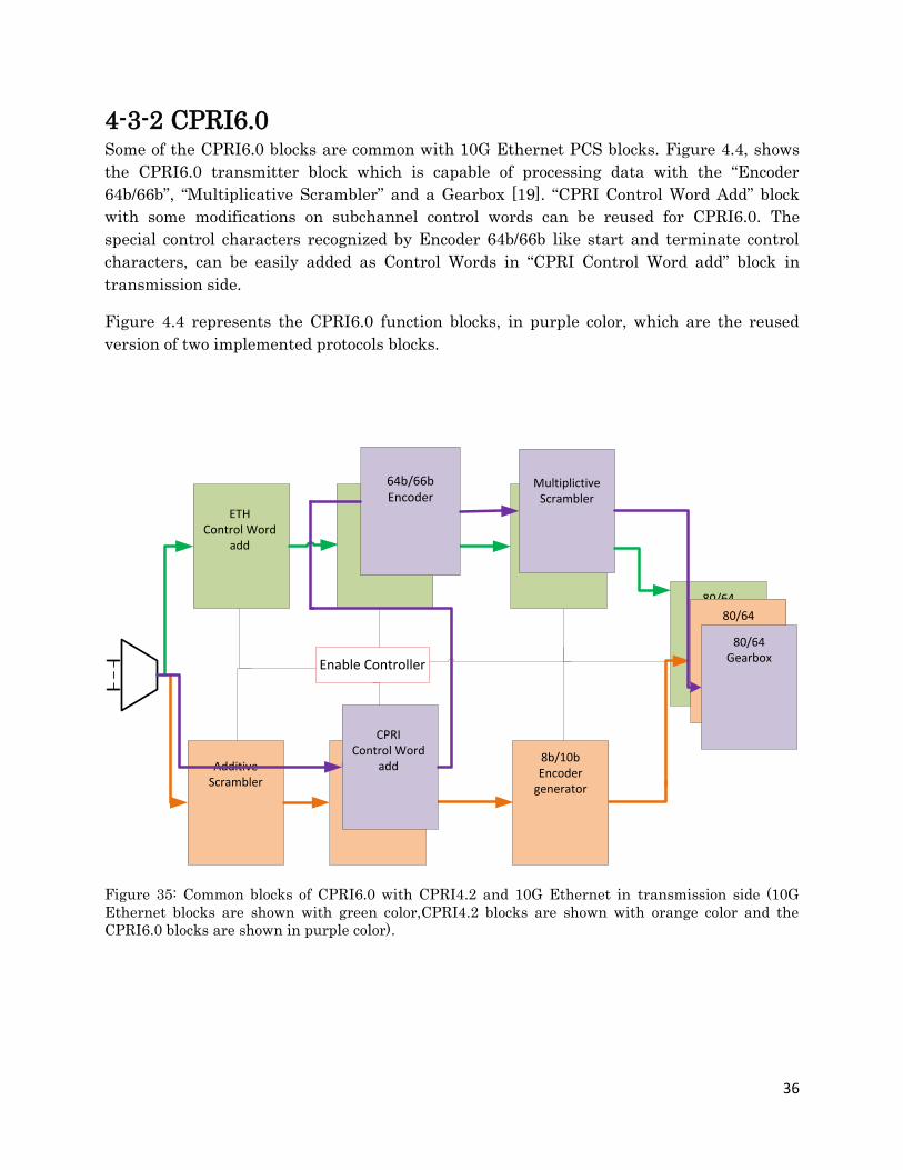
4-3-2 CPRI6.0 Some of the CPRI6.0 blocks are common with 10G Ethernet PCS blocks. Figure 4.4, shows
the CPRI6.0 transmitter block which is capable of processing data with the “Encoder
64b/66b”, “Multiplicative Scrambler” and a Gearbox [19]. “CPRI Control Word Add” block
with some modifications on subchannel control words can be reused for CPRI6.0. The
special control characters recognized by Encoder 64b/66b like start and terminate control
characters, can be easily added as Control Words in “CPRI Control Word add” block in
transmission side.
Figure 4.4 represents the CPRI6.0 function blocks, in purple color, which are the reused
version of two implemented protocols blocks.
Figure 35: Common blocks of CPRI6.0 with CPRI4.2 and 10G Ethernet in transmission side (10G
Ethernet blocks are shown with green color,CPRI4.2 blocks are shown with orange color and the
CPRI6.0 blocks are shown in purple color).
ETHControl Word
add dout
MultiplictiveScrambler
64b/66bEncoder
dout
80/64Gearbox
CPRIControl Word
AddAdditive
Scrambler
8b/10bEncoder
generator
64
Enable Controller
MultiplictiveScrambler
dout
80/64Gearbox
80/64Gearbox
64b/66bEncoder
CPRIControl Word
add

37
4-3-3 1G/2G/4G Fibre Channel 1/2/4G Fibre Channel protocol uses “Encoder 8b/10b”, and Gearbox in the transmission side
which are in common with CPRI4.2 [20]. As Fibre Channel uses 8b/10b Encoding scheme in
the transmission side, “CPRI control Word add” block with some modifications on
subchannel control words can be reused for Fibre Channel protocol. Figure 4.5 shows parts
of the transmitter block for 1/2/4G Fibre Channel.
Figure 36: Common blocks among 1/2/4Gbps Fibre Channel and CPRI4.2 in transmission side (10G
Ethernet blocks are shown with green color, CPRI4.2 blocks are shown with orange color and the
1/2/4G Fibre channel blocks are shown in grey color).
ETHControl Word
add
MultiplictiveScrambler
64b/66bEncoder
dout
80/64Gearbox
cout
CPRIControl Word
AddAdditive
Scrambler
dout
8b/10bEncoder
generator
64
Enable Controller dout
80/64Gearbox
CPRIControl Word
Add
8b/10bEncoder
generator
80/64Gearbox

38
4-3-4 Model Application Summery The implemented model can be reused for several protocols such as xIO-s, CPRI6.0, 1/2/4G
Fibre Channel. Although these protocols have other functions, but common functions can be
shared with other protocols.
Figure 4.6 depicted the shared common function between 10GEthernet, CPRI4.2, CPRI6.0,
xIO-s, 1/2/4G Fibre Channel in a transmitter block. If they are designed with a fixed
solution instead of flexible blocks, 19 blocks should be implemented. With flexible solution, 7
blocks are implemented.
Figure 37: Common blocks among 10G Ethernet,CPRI4.2, xIO-s, CPRI6.0, 1/2/4Gbps Fibre Channel
in transmission side (10G Ethernet blocks are in green color, CPRI4.2 blocks are in orange color, xIO-
s blocks are in blue color,CPRI6.0 blocks are in purple and the 1/2/4G Fibre channel blocks are shown
in grey color).
ETHControl Word
add dout
MultiplictiveScrambler
64b/66bEncoder
dout
80/64Gearbox
cout
CPRIControl Word
AddAdditive
Scrambler
dout
8b/10bEncoder
generator
64
Enable Controller
MultiplictiveScrambler
dout
80/64Gearbox
CPRIControl Word
Add
8b/10bEncoder
generator
80/64Gearbox
MultiplictiveScrambler
80/64Gearbox
64b/66bEncoder
CPRIControl Word
addCPRI
Control Word Add
8b/10bEncoder
generator
80/64Gearbox

39
5 Results
5-1 Simulation Result
In this section, the example of working a test case for each case study protocols is shown.
5-1-1 10G Ethernet Simulation Result
The 10G Ethernet test vectors are applied to the transmitter input. An example of a 64 bits
test vector, simulated in ModelSim, is shown in the figure 5.1 with the value of
“abaaaaaaaaaaaaaa” in hexadecimal. Data is recovered in the reception side after some
cycles. The order of data transfer is as follow:
Control Words are added to the data.
Data is encoded.
Data is scrambled.
Data is sent to the transmitter output (and receiver input) via the transmitter
gearbox.
Data is passed through the receiver gearbox.
Data is descrambled.
Data is decoded.
Control words are deleted and input data is recovered after some cycles.
Figure 38: 10G Ethernet test case simulation.

40
5-1-2 CPRI4.2 Simulation Result
The CPRI4.2 test vectors are applied to transmitter inputs. In figure 5.2 , an example of 64
bits test vector, simulated in ModeSim, is shown with the value of “01c1c1c1c1c1c1c1” in
hexadecimal.The sequence of functions is as follows:
Data is scrambled.
Control Words are added to the scrambled data.
Data is encoded.
Data is sent to the transmitter output (and receiver input) via the transmission
gearbox.
Data is passed through receiver gearbox.
Data is decoded.
Control Words are deleted and test vector is recovered after some cycles.
Figure 39: CPRI4.2 test case simulation.
5-2 Synthesis Result
The evaluation of the synthesis results and comparison of them with other implementation
solutions are out of this thesis scope.
In below tables, the results show that the codes are synthesizable and there is a possibility
of running them in a proper frequency of approximately 1G.Blocks were synthesized in
Synopsys in 28nm technology.
As can be seen, the results are reasonable in terms of area (cell area) and complexity
(number of cells).

41
Table 5: Synthesis Results.
ETH add CW 2513 3301 907
ETH del CW 2543 2926 915
CPRI add CW 2563 3949 962
CPRI del CW 2773 4168 969
Multiplicative Scrambler 432 798 997
Multiplicative Descrambler 489 739 999
Encoder 64b/66b 878 1543 973
Decoder 64b/66b 778 1447 977
Encoder 8b/10b 163 256 912
Decoder 8b/10b 150 192 999
Gearbox 5212 7666 951
Function Block Number of Cells Total Area Frequency [MHz]

42
6 Conclusions and Future Work
6-1 Conclusions
This work investigated the feasibility of the reconfigurable network processor
implementation in RTL level.
It is concluded that it is possible to implement a runtime flexible programmable network
unit processor in RTL level which is flexible both in block level and in system level.
Block level flexibility
In this study, common blocks of two case studies (10G Ethernet and CPRI4.2) are
implemented with the help of parameterized SystemlogVerilog blocks.
Both types of add/delete control word blocks are implemented for 10G Ethernet and
CPRI4.2 (all bit rates). With small modification in control word add/delete blocks,
they can be reused for other protocols. For example, with adding the start and
terminate characters as subchannel control words in the “CPRI Control Word add
block”, this block can be reused for CPRI6.0.
Both types of additive and multiplicative Scrambler/Descrambler are implemented
with generic data width and polynomial. They can cover other protocols which use
one of the Scrambler/Descrambler type with a different polynomial.
Both types of 64b/66bEncoder/Decoder and 8b/10bEncoder/Decoder, which are the
most common encoding/decoding schemes in communication protocols, are
implemented.
Generic Gearbox is implemented with any effective bit rate.
System level flexibility
The system is reconfigurable for two different case study protocols by the muxing structure.
The model can be reconfigured for other protocols with the common function blocks.
Other protocols with bypass mode for functions which are not needed for some
applications. For instance, 1/2/4G Fibre Channel which uses the same order of
CPRI4.2 function blocks with a bypass mode for the scrambler.
Other protocols can reuse the combination of two case studies blocks. For example,
CPRI6.0 and xIO-s blocks are the mixture of both implemented case studies blocks.

43
6-2 Recommendations
It is recommended to Ericsson AB to implement the reconfigurable network processor in the
next generation EMCA’s. This recommendation is based on the following facts concluded
from this work.
As most of network protocols are very similar in the function blocks, it is possible to
find common functions between different protocols. In this study, common functions
of 10G Ethernet and CPRI4.2 are found.
It is possible to implement common blocks in a flexible way in order to use them for
different protocols. In this work, the flexible block implementation is done via
parameterized SystemlogVerilog blocks concept.
It is possible to make a flexible connection between common generic blocks. In this
work it is done via muxing structure. It can be done with other solutions like
switches or a control processor to connect the blocks.
It is possible to reuse the implemented system for other protocols rather than this
work use cases. For example, it is investigated that it is possible to use the
implemented blocks for CPRI6.0, xIO-s, 1/2/4G Fibre Channel.
It is easy to modify the RTL blocks code to support other protocols functionalities.
This work studied the possibility of making some modifications on CPRI Control
Word add/delete block to support CPRI6.0, Fibre Channel Control word add/delete.
However, some factors should be considered as the concerns of reconfigurable network
processor implementation.
Reconfigurable network protocol processor is complex both in design and verification
phases. It is a complex work to design a network processor which can handle
different protocols. Also, it is complex verification effort to test generic and
reconfigurable designs.
A configuration environment should be developed to set up the different protocols at
the reset time.

44
6-3 Future Work
To use reconfigurable network processor in next generation Ericsson’s EMCAs, future
implementation and development is offered.
Future investigation need to be done on the comparison between reconfigurable
network processor and today network processor ASICs. This comparison should
clarify the compromise between two solutions in terms of work cost, area cost,
complexity, power and memory.
The Implemented reconfigurable network processor should be studied in terms of
capacity (how many functions and fifos are needed) and performance (how many
packets can be transmitted per second).
Different use cases protocols should be described in software level via a configuration
file. The development configuration environment should describe the protocol of
choices at the reset time with own functions to be implemented.

45
References
[1] Sara Karlsson. (2013). Master Thesis in System on Chip at the University of Linköping: Micro NPU for Baseband Interconnect. Retrieved from
http://www.diva-portal.org/smash/get/diva2:690145/FULLTEXT01.pdf
[2] International Standard. ISO/IEC 7498-1(1994).Information technology-Open system
Interconnections-Basic Reference Model: The Basic Model. Retrieved from
http://www.ecma-international.org/activities/Communications/TG11/s020269e.pdf
[3] IEEE Standard for Information technology-Telecommunications and information
exchange between systems-Local and metropolitan area networks-Specific requirements,
IEEE Standard 802.3ae, 2002.
[4] Siwaruk Siwamogsatham.10 Gigabit Ethernet. Retrieved from
http://www.cse.wustl.edu/~jain/cis788-99/ftp/10gbe/
[5] Common Public Radio Interface (CPRI),Interface Specification, CPRI Specification
V4.2,2010.
[6] CPRI basics [PowerPoint slides]. Retrieved from
http://www.mrdata.se/wrapper/CPRI%20basics_PA4.pdf
[7] Byeong Gi Lee,& Byoung-Hoon Kim (2001). Scrambling Techniques for CDMA
Communications.Massachusetts:Kluwer Academic Publishers.
[8] Block 5: Part 1, Channel Coding. [PowerPoint slides]. Retrieved from
https://www.google.com/search?q=%22Figure+Channel+coding+by+scrambling%22
[9] Dr. Martin Miller(2005). TRANSITION DENSITY: WHAT DOES IT AFFECT AND
WHY IS IT EXPLICITLY SPECIFIED WITHIN THE LECROY SDA? [PDF document].
Retrieved from
http://cdn.teledynelecroy.com/files/whitepapers/wp_techbrief_trans_den.pdf
[10] Chapter 4,Digital Transmission. Data communication and networking [PDF
document].Retrieved from
http://sparc.nfu.edu.tw/~lyc/intro_net/ch04.pdf
[11] Dr. Johnson.(2002). Fiber-Optic Encoding. Retrieved from
http://www.sigcon.com/Pubs/edn/FiberOpticEncoding.htm
[12] Jeff Mandin (2006). Scrambling in 10G Ethernet and applicability. [PDF document].
Retrieved from
http://www.ieee802.org/3/av/public/2006_11/3av_0611_mandin_1.pdf

46
[13] IET, NTNU. Line codes and scrambling [PDF document]. Retrieved from
http://www.iet.ntnu.no/courses/ttt4130/lecturenotes/Linecodes.pdf
[14]PeterJ. 8B/10B Coding,64B/66B Coding[PowerPoint slides]. Retrived from
http://www.nikhef.nl/~peterj/KM3net/8B10B_Coding.pdf
[15] Al X. Widmer, Peter A. Franaszek (1983). "A DC-Balanced, Partitioned-Block, 8B/10B
Transmission Code". IBM Journal of Research and Development 27 (5): 440.
[16] LATTICE SEMICONDUCTOR(2012). 8b/10b Encoder/Decoder. Reference Design
RD1012. Retrieved from
http://www.latticesemi.com/~/media/Documents/ReferenceDesigns/1D/8b10bEncoderDecode
r-Documentation.PDF
[17] Peter A. Franaszek, Albert X. Widmer (1984). US patent 4486739 A. U.S.
[18] Ericsson document: IWD_L2_xIO-s.doc, 2013-04-04.
[19] Common Public Radio Interface (CPRI),Interface Specification,CPRI Specification
V6.0,2013.
[20] More than IP, 1/2/4/8Gbps Fibre Channel Transport Core, Version 1.1, April 2011.