Design Automation for Reconfigurable Interconnection Networks
12
© The Author 2012. Published by Oxford University Press on behalf of The British Computer Society. All rights reserved. For Permissions, please email: [email protected] doi:10.1093/comjnl/bxs136 Design Automation Framework for Reconfigurable Interconnection Networks Hongbing Fan 1 , Yu-Liang Wu 2 and Ray C.C. Cheung 3,∗ 1 Wilfrid Laurier University,Waterloo, ON, Canada 2 The Chinese University of Hong Kong, Shatin, N.T., Hong Kong 3 City University of Hong Kong, KowloonTong, Hong Kong ∗ Corresponding author: [email protected] A reconfigurable interconnection network (RIN) is a custom-designed on-chip switching network yielding routing solutions for a pre-given set of applications. Like field programmable gate array (FPGA) routing networks, the RIN is used to make reconfigurable interconnections among functional blocks. Unlike FPGAs, the network topology of a RIN is irregular as it is designed for a given set of routing requirements and optimized for the area cost subject to given delay constraints. In this paper, we propose an automatic design scheme for RINs, including routing specification formulation, graph modelings, network topology designs, routing algorithms and multiplexer-based network circuit implementation. The choice of the design scheme is based on the existing routing network design practices and research, which give feasible solutions. Our scheme is to optimize the designs with the choice of design parameters. A computer-aided design (CAD) tool is developed based on the design scheme, which takes a set of routing requirements as input and produces the corresponding RIN network topology and network circuit in hardware description language format. We present the area costs of various RINs generated by the CAD tool subject to delay constraints, and illustrate the RIN design scheme with a reconfigurable multistream video system. Keywords: interconnection network; routing network; computer-aided design; optimization Received 9 November 2011; revised 8 August 2012 Handling editor: Terrence Mak 1. INTRODUCTION Our study on reconfigurable interconnection networks (RINs) was motivated by the design of reconfigurable system- on-chips (SoCs) for a pre-given set of applications. The system can be reconfigured to run one application at a time, or several applications simultaneously. Each application requires a subgroup of available functional blocks (FBs), whose interconnections form a routing requirement determined by the application. An RIN is used to make the various interconnections of the FBs for different applications. Since the RIN is for a pre-given set of applications, it can be specifically designed and optimized for resource usage subject to delay constraints. This motivates us to consider the general RIN design optimization problem; that is, given a set of routing requirements, to design a switching network feasible to route each of the given routing requirements while having low area, power and delay costs. Figure 1a shows the application of RINs in a reconfigurable multistream video system, where the RIN is used to switch stream-video signals going through different processing units. Figure 1b shows the block diagram of the RIN, in which the switching module consists of wires and switches that connect input ports to output ports. The ON/OFF of switches are con- trolled by control bits stored in the configuration registers, which are loaded through load registers. The load registers receive data through address and configuration data paths with a decoder. The idea of using an RIN as a reconfigurable component in a reconfigurable system has been previously discussed. In [1], Li and Chakrabarty presented an RIN solution for deterministic built-in self-testing (BIST), in which an RIN is placed between The Computer Journal, 2012 The Computer Journal Advance Access published October 10, 2012 at City University of Hong Kong on July 16, 2013 http://comjnl.oxfordjournals.org/ Downloaded from
-
Upload
independent -
Category
Documents
-
view
10 -
download
0
Transcript of Design Automation for Reconfigurable Interconnection Networks
© The Author 2012. Published by Oxford University Press on behalf of The British Computer Society. All rights reserved.For Permissions, please email: [email protected]
doi:10.1093/comjnl/bxs136
Design Automation Framework forReconfigurable Interconnection
Networks
Hongbing Fan1, Yu-Liang Wu
2and Ray C.C. Cheung
3,∗
1Wilfrid Laurier University, Waterloo, ON, Canada2The Chinese University of Hong Kong, Shatin, N.T., Hong Kong
3City University of Hong Kong, Kowloon Tong, Hong Kong∗Corresponding author: [email protected]
A reconfigurable interconnection network (RIN) is a custom-designed on-chip switching networkyielding routing solutions for a pre-given set of applications. Like field programmable gate array(FPGA) routing networks, the RIN is used to make reconfigurable interconnections among functionalblocks. Unlike FPGAs, the network topology of a RIN is irregular as it is designed for a given set ofrouting requirements and optimized for the area cost subject to given delay constraints. In this paper,we propose an automatic design scheme for RINs, including routing specification formulation, graphmodelings, network topology designs, routing algorithms and multiplexer-based network circuitimplementation. The choice of the design scheme is based on the existing routing network designpractices and research, which give feasible solutions. Our scheme is to optimize the designs with thechoice of design parameters. A computer-aided design (CAD) tool is developed based on the designscheme, which takes a set of routing requirements as input and produces the corresponding RINnetwork topology and network circuit in hardware description language format. We present the areacosts of various RINs generated by the CAD tool subject to delay constraints, and illustrate the RIN
design scheme with a reconfigurable multistream video system.
Keywords: interconnection network; routing network; computer-aided design; optimization
Received 9 November 2011; revised 8 August 2012Handling editor: Terrence Mak
1. INTRODUCTION
Our study on reconfigurable interconnection networks (RINs)was motivated by the design of reconfigurable system-on-chips (SoCs) for a pre-given set of applications. Thesystem can be reconfigured to run one application at atime, or several applications simultaneously. Each applicationrequires a subgroup of available functional blocks (FBs),whose interconnections form a routing requirement determinedby the application. An RIN is used to make the variousinterconnections of the FBs for different applications. Since theRIN is for a pre-given set of applications, it can be specificallydesigned and optimized for resource usage subject to delayconstraints. This motivates us to consider the general RINdesign optimization problem; that is, given a set of routingrequirements, to design a switching network feasible to route
each of the given routing requirements while having low area,power and delay costs.
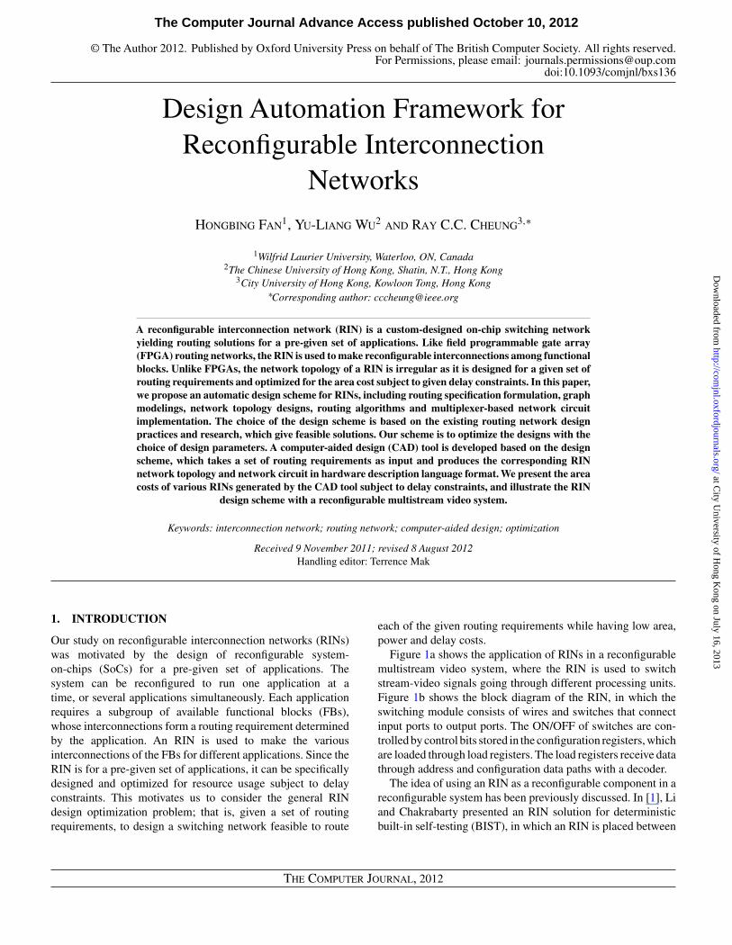
Figure 1a shows the application of RINs in a reconfigurablemultistream video system, where the RIN is used to switchstream-video signals going through different processing units.Figure 1b shows the block diagram of the RIN, in which theswitching module consists of wires and switches that connectinput ports to output ports. The ON/OFF of switches are con-trolled by control bits stored in the configuration registers, whichare loaded through load registers. The load registers receive datathrough address and configuration data paths with a decoder.
The idea of using an RIN as a reconfigurable component in areconfigurable system has been previously discussed. In [1], Liand Chakrabarty presented an RIN solution for deterministicbuilt-in self-testing (BIST), in which an RIN is placed between
The Computer Journal, 2012
The Computer Journal Advance Access published October 10, 2012 at C
ity University of H
ong Kong on July 16, 2013
http://comjnl.oxfordjournals.org/
Dow
nloaded from
2 H. Fan et al.
I1
I3
CRIN_AD
C2
Switching
I1
I2
I2
I2
C1
RIN
P1
P2
P4
O1 O2 O3
Memory
Block 1Multi−portSDRAMcontrol
Processor
Bus
RIN
C2P3
moduleI2I3
Block 2
Memory
Load registers
Reconfigurable multi−stream video system Components of RIN.
P3P3P2P1
C1moduleSwitching
Configuration registersRES
CFIG_EN
CS
LOAD_EN
CRIN_CD
Switch controller
Decoder
(a) (b)
FIGURE 1. RIN and its application in reconfigurable systems. (a) Reconfigurable multistream video system. (b) Components of RIN.
p1
p0
x2x1
RIN p0 p1 p2 p3 p4
p4q4
q5
q6q2
M2
q3M3
p3
p2
q1
M1
q7
q1 q2 q3 q4 q5 q6 q7
FIGURE 2. RIN for fault-tolerant system design.
the outputs of a pseudo-random pattern generator and the scaninputs of the circuit under test. The RIN approach achievesless hardware overhead and fewer control bits compared withother hybrid BIST approaches. Figure 2 depicts a reconfig-urable triple module redundancy fault-tolerant design usingan RIN. In these application instances, an RIN serves anapplication-specific FB satisfying a given routing specification(RS). After it is designed, it is added into the host design,followed by the standard IC design flow for the floor plan androuting. Even though RINs or alike components have been usedin many applications, there are no systematic design schemesand design automation tools for RINs.
Field programmable gate arrays (FPGAs) routing networkdesign provides an approach for RIN designs, as the routingnetworks in FPGAs are used to perform the reconfigurable inter-connection of configurable logic blocks [2, 3]. However, FPGArouting networks are designed to have high routability for
genetic functions, and they tend to have higher area and powercosts [4]. Custom FPGAs of different sizes and shapes subjectto area constraints of programmable SoCs were discussedin [5]. In [6], Parvez et al. proposed application-specificFPGAs, which reduces the area usage by removing the unusedrouting resources from regular FPGA routing networks.
We propose an approach that designs an RIN directly from anRS. As a result, an application-specific RIN is derived, whichusually comes with an irregular topology and varies accordingto the RSs. The irregularity of the application-specific RINmakes it difficult with regard to design and fabrication as well asin finding routing configurations for the applications. However,the design difficulties are reduced with the help of computer-aided design (CAD) tools and routing difficulties by storingthe pre-computed configurations for the given set of applica-tions. This paper presents the RIN design scheme and CADtools. The design scheme deals with both hardware and soft-ware. The hardware part involves RS, network topology designand network circuit design. The software part deals with thetopology generation, circuit generation and routing. The CADtools take a set of routing requirements as input and producesa corresponding RIN topology and circuit in hardware descrip-tion language (HDL) format, and then generates the routingfor the specified application.
The rest of this paper is organized as follows. Section 2gives the formulation of RS and RIN design problems and acombinatorial circuit method for directed RIN design. Section 3presents the network topology designs for directed RINs,including 1-stage crossbars, multistage Clos networks andour generalized Clos networks. Section 4 gives the topologydesigns for undirected RINs. Section 5 describes the RIN designautomation flow together with the corresponding CAD tools.Section 6 presents the experimental results underAltera QuartusII for a variety of RIN circuits and the RIN-based reconfigurablemultistream video system.
The Computer Journal, 2012
at City U
niversity of Hong K
ong on July 16, 2013http://com
jnl.oxfordjournals.org/D
ownloaded from
Design Automation Framework for RIN 3
2. RIN DESIGN SPECIFICATIONS
This section gives the general formulations for routingrequirements, RS and the RIN design problem, followed bythe combinatorial circuit method for RIN design.
2.1. Routing specifications
The function of an RIN is to make required interconnectionsof the ports of FBs according to application specifications.The set of FBs contains all the fundamental blocks tobe used in the anticipated applications. Each FB containsinput/output/inout pins. An application uses a subset of theFBs with specific interconnections of their pins. The termnet refers to an interconnection request of two or morepins. A net is a 2-pin net (or point-to-point connection) if itconnects an output pin (source) to an input pin (sink), andis a multipin net (or one-to-many connection) if it connectsan output pin to two or more input pins. An inout pin canfunction either as an input pin or output pin. A realization(or routing) of a net is a physical connection of the pinsby wires and ON switches. An application corresponds toa set of disjoint nets, which is referred to as a routingrequirement.
In a pure ASIC design, there is only one routing requirementspecified by one application. The routing problem is todetermine how to lay out the wires to realize all the nets of therouting requirement. When the multiple application design isconsidered, a super set of FBs and a set of routing requirementsover the pins are given. We consider using an RIN to realizeall the given routing requirements after the system is fabricatedand when the system is in use. As an FB, the input (output,inout) pins of the RIN will be connected to the output (input,inout) pins of other FBs. To avoid confusion, we use theterm input (output, inout) port to refer to the input (output,inout) pin when designing a RIN. Then the sets of input,output and inout ports and the set of routing requirements overthe ports form the RS of an RIN design. It is formulated asfollows.
Let A, B and U denote the sets of input, output and inoutports, respectively. A net N (or (t + 1)-pin net) connectingan input/inout port p0 ∈ A ∪ U to some output/inout portsp1, . . . , pt ∈ B ∪ U is represented as N = {p0, p1, . . . , pt }.A routing requirement consists of a set of disjoint nets,represented as R = {Ni : i = 1, . . . , k}, where each Ni
is a net and Ni ∩ Nj = ∅ if i �= j . A set of routingrequirements is represented as C = {R1, . . . , Rs}, where eachRj = {Nji
: i = 1, . . . , kj } is a routing requirement forj = 1, . . . , s. Then the RS is formulated as the quadruple(A, B, U, C).
An RIN satisfying RS (A, B, U, C) is a module consisting ofwires and switches connecting ports of A, B, U and satisfyingthat, for each routing requirement R ∈ C, there are ON/OFFassignments of the switches so that all nets in R are realizedand two different nets are disjoint.
2.2. RS simplification
The RS (A, B, U, C) is derived directly from the ports of otherFBs and the set of routing requirements associated with theapplications. It can be simplified without affecting the designof the RIN. For example, if a net is contained in every routingrequirement, then a fixed routing of the net will satisfy therequirement. Therefore, the net can be removed from the RS.It is proved that the following reduction rules can be used forsimplification.
(R1) If a ∈ A ∪ B ∪ U is not contained in any net, removea from A ∪ B ∪ U .
(R2) Remove all nets N such that |N | = 1.(R3) If a net N is contained in every routing requirement of
C, then remove N from all the requirements.(R4) If {a, a′} is the only net containing a, then remove net
{a, a′} from C. In this case, switches joining a to a′must be added to the RIN.
Repeatedly applying the above rules to the resulting RS untilno further reductions can be done, we obtain a reducedRS (A, B, U, C). Furthermore, we decompose (A, B, U, C)
into minimal RSs (Ai, Bi, Ui, Ci), i = 1, . . . , k, whereAi, Bi, Ui, i = 1, . . . , k are mutually disjoint and a minimalRS is one which cannot be decomposed further. We need onlyconsider the problem of designing an RIN for a minimal RSbecause the RIN for a non-minimal RS is the union of RINs ofall its minimal RSs.
We consider two types of RSs, directed and undirected. Adirected RS contains no inout ports, i.e. U = ∅, denotedby (A, B, C). We use directed RINs consisting of wires andunidirectional switches for a directed RS.An undirected RS onlycontains inouts ports, i.e. A = B = ∅, denoted by (U, C), andwe use an undirected RIN consisting of wires and bidirectionalswitches for an undirected RS. If A ∪ B �= ∅ and U �= ∅,we treat all ports as inout ports and design an undirected RINaccordingly.
2.3. Combinational circuit design for RINs
The straight solution for a directed RIN design is by acombinational circuit method in the following steps: (i)determine the number of control bits, and assign a code patternof the control bits for each of the routing requirements; (ii)represent each output variable by a Boolean expression of inputvariables and control variables; (iii) apply the combinationallogic technique to optimize the Boolean expression/circuit so asto minimize the number of switches and delays; and (iv) derivean RIN circuit from the Boolean expressions. The followingexample illustrates the combinational approach.
As shown in Fig. 2, three redundancy computing mod-ules M1, M2 and M3, and a majority comparator M aregiven. The output and input ports are A = {p0, p1, . . . ,
p4} and B = {q1, . . . , q7}. The given routing require-ments are: R1 = {{p0, q1}, {p1, q7}}, R2 = {{p0, q2},
The Computer Journal, 2012
at City U
niversity of Hong K
ong on July 16, 2013http://com
jnl.oxfordjournals.org/D
ownloaded from
4 H. Fan et al.
{p2, q7}}, R3 = {{p0, q3}, {p4, q7}}, R4 = {{p0, q1, q2, q3},{p1, q4}, {p2, q5}, {p3, q6}, {p4, q7}}. Here, each of R1, R2 andR3 uses only one of the three redundant modules, and so it ispower efficient but not fault-tolerant. The R4 uses all the threemodules and the comparator; it is a fault-tolerant design for thecomputation module. That is, if one of the three modules fails,the system still has the correct output.
Since there are four routing requirements, we can use twocontrol bits x1, x2. Then the RIN to be designed has inputvariables {x1, x2, p0, . . . , p4} and output variables {q1, . . . , q7}.
We assign a code pattern of control bits x1x2 for R1, . . . , R4
as 00, 01, 10, 11, respectively. Then relations of input/outputvariables determined by the given set of routing requirementscan be represented by the following Boolean expressions:q1 = x ′
1x′2p0 + x1x2p0, q2 = x ′
1x2p0 + x1x2p0, q3 =x1x
′2p0 + x1x2p0, q4 = x1x2p1, q5 = x1x2p2, q6 = x1x2p2,
q7 = x ′1x
′2p1 + x ′
1x2p2 + x1x′2p3 + x1x2p4. A combinational
circuit for the above Boolean expressions can be derived byusing the existing combinatorial logic design technique.
In general, if there are t different routing requirements, theminimum number of control bits is log2 t. The number ofdifferent routing requirements to code pattern assignments is t !.It would be impossible to try all possible assignments for anoptimum assignment when t is large, say t ≥ 8. On the otherhand, since at least one output port will appear in at least t/n
different requirements, where n is the number of input ports,the number of terms in the Boolean expression is at least t/n.The evaluation of a Boolean expression with a bounded fan-in logic gate will have O(log t/n) gate delays. For instance,when designing an RIN capable of routing all possible routingrequirements from m outputs to n input ports. The number ofrouting requirements is equal to
∑ni=0 S(n, k)m(m−1) · · · (m−
k+1) = mn, where S(n, k) is the Stirling number of the secondkind, which counts the number of ways to partition a set of n
elements into k non-empty subsets. The minimum number ofcontrol bits is m log n. Particularly, when m = n = 8, thenumber of routing requirements is 16 777 216 and the number ofcontrol bits is 24, it is impossible to use the above combinationalapproach to find an optimal RIN design due to the number of
possible assignments between routing requirements and codepatterns and the size of Boolean expressions.
Next, we consider the switching network approach for RINdesign. The main tasks of the network approach are the networktopology design, network circuit design and finding routings forthe given routing requirements.
3. DESIGN FOR DIRECTED RINS
In this section, we consider the topology design and circuitimplementation for directed RS (A, B, C). We first give thegraph modeling for directed RINs and multiplexer (MUX)-based implementation and then present four candidate topologydesigns in the trade-off in the use of different resources.
3.1. Graph modeling and implementations
We model a directed RIN for (A, B, C) by a multistage digraph.A k-stage digraph is a digraph G = (V0 ∪ · · · ∪ Vk, E), whereV0, . . . , Vk are disjoint node sets, and each edge (or arc) in E
is from a node in Vi to a node in Vj with j > i. If every edgeis joining a node of Vi to a node of Vi+1, we call it a k-stagebipartite digraph. Particularly, A = V0 are input nodes andB = Vk are output nodes, and nodes in Vi, 1 ≤ i ≤ k − 1, areintermediate nodes.
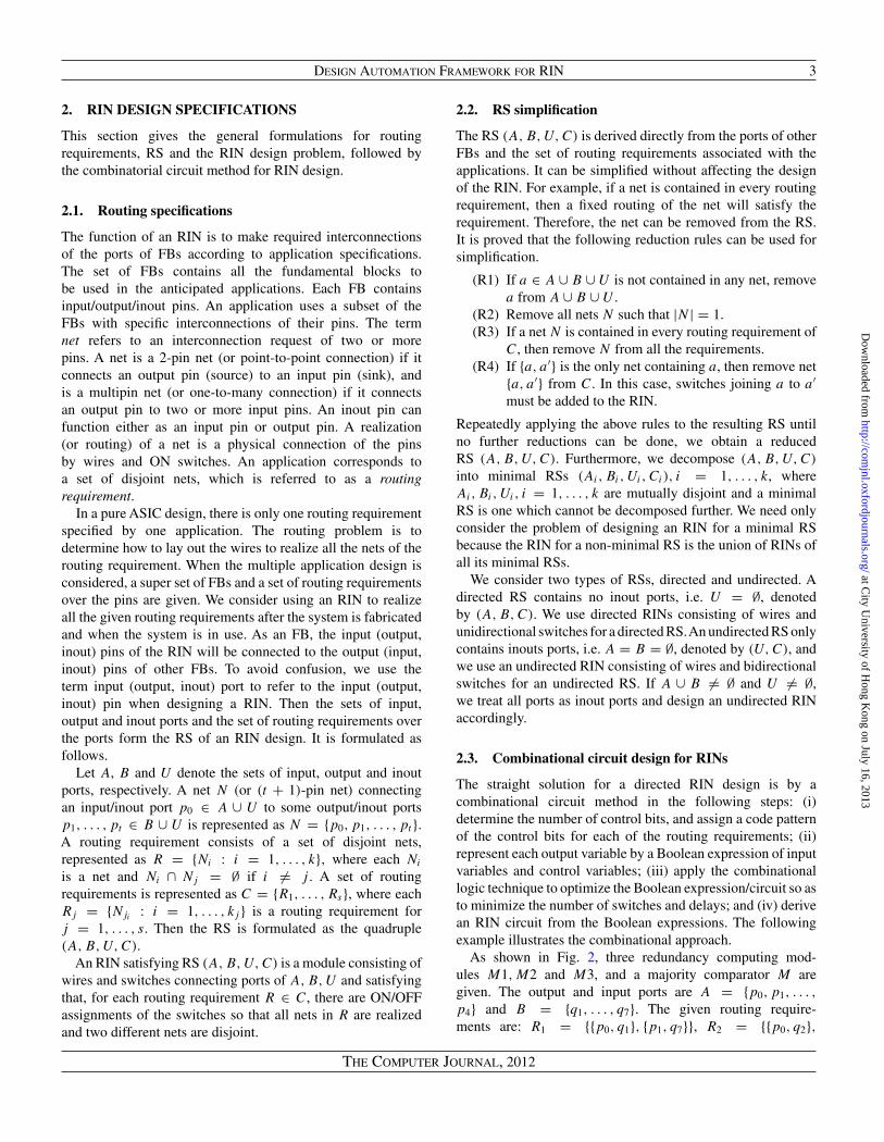
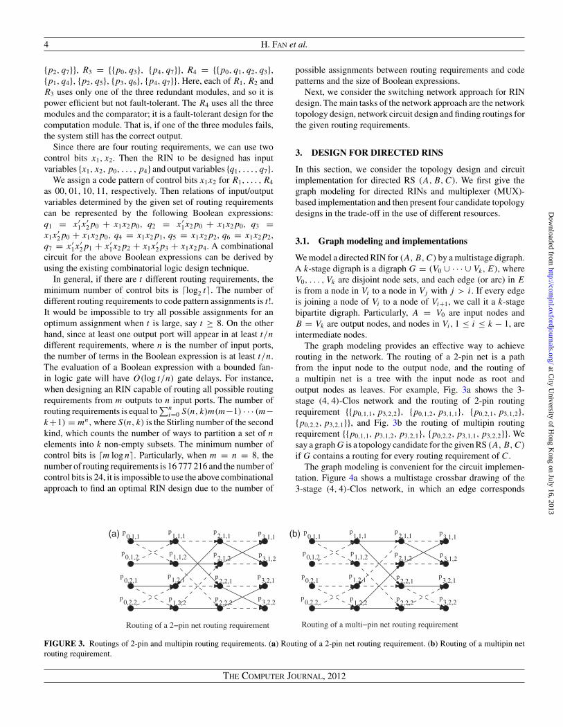
The graph modeling provides an effective way to achieverouting in the network. The routing of a 2-pin net is a pathfrom the input node to the output node, and the routing ofa multipin net is a tree with the input node as root andoutput nodes as leaves. For example, Fig. 3a shows the 3-stage (4, 4)-Clos network and the routing of 2-pin routingrequirement {{p0,1,1, p3,2,2}, {p0,1,2, p3,1,1}, {p0,2,1, p3,1,2},{p0,2,2, p3,2,1}}, and Fig. 3b the routing of multipin routingrequirement {{p0,1,1, p3,1,2, p3,2,1}, {p0,2,2, p3,1,1, p3,2,2}}. Wesay a graph G is a topology candidate for the given RS (A, B, C)
if G contains a routing for every routing requirement of C.The graph modeling is convenient for the circuit implemen-
tation. Figure 4a shows a multistage crossbar drawing of the3-stage (4, 4)-Clos network, in which an edge corresponds
p
p
p
p
p
p
p
p p
p
p
p
p
p
p
p p
p
p
p
p
p
p
p p
p
p
p
p
p
p
p0,1,1
0,1,2
0,2,1
0,2,2
1,1,1
1,1,2
1,2,1
1,2,2
2,1,1
2,1,2
2,2,1
2,2,2
3,1,1
3,1,2
3,2,1
3,2,2
0,1,1
0,1,2
0,2,1
0,2,2
1,1,1
1,1,2
1,2,1
1,2,2
2,1,1
2,1,2
2,2,1
2,2,2
3,1,1
3,1,2
3,2,1
3,2,2
Routing of a 2−pin net routing requirement Routing of a multi−pin net routing requirement
(a) (b)
FIGURE 3. Routings of 2-pin and multipin routing requirements. (a) Routing of a 2-pin net routing requirement. (b) Routing of a multipin netrouting requirement.
The Computer Journal, 2012
at City U
niversity of Hong K
ong on July 16, 2013http://com
jnl.oxfordjournals.org/D
ownloaded from
Design Automation Framework for RIN 5
p
p
p
p
0,1,1
0,1,2
0,2,1
0,2,2p
p
p
p
2,1,1
2,1,2
2,2,1
2,2,2
Clos network in multistage crossbar
p
p p
p
p
p
p
p
p
p
p
p
p
p
p p
p
p
p
p p
p1,1,1
1,1,2
1,2,1
1,2,2
3,1,1 3,2,1
0,1,1
0,1,2
0,2,1
0,2,2
1,1,1
1,1,2
1,2,1
1,2,2
2,1,1
2,1,2
2,2,1
2,2,2
3,1,1
3,1,2
3,2,1
3,2,2
p3,1,2p
3,2,2
(a) (b)
Clos network in multiplexors
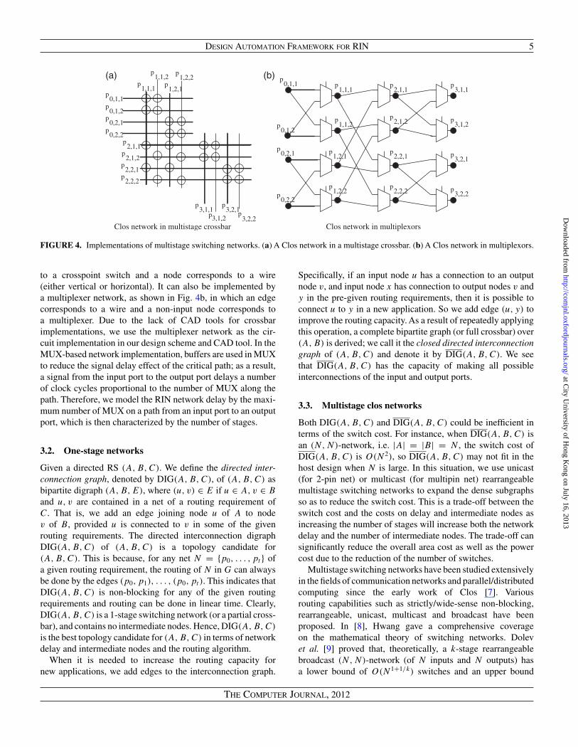
FIGURE 4. Implementations of multistage switching networks. (a) A Clos network in a multistage crossbar. (b) A Clos network in multiplexors.
to a crosspoint switch and a node corresponds to a wire(either vertical or horizontal). It can also be implemented bya multiplexer network, as shown in Fig. 4b, in which an edgecorresponds to a wire and a non-input node corresponds toa multiplexer. Due to the lack of CAD tools for crossbarimplementations, we use the multiplexer network as the cir-cuit implementation in our design scheme and CAD tool. In theMUX-based network implementation, buffers are used in MUXto reduce the signal delay effect of the critical path; as a result,a signal from the input port to the output port delays a numberof clock cycles proportional to the number of MUX along thepath. Therefore, we model the RIN network delay by the maxi-mum number of MUX on a path from an input port to an outputport, which is then characterized by the number of stages.
3.2. One-stage networks
Given a directed RS (A, B, C). We define the directed inter-connection graph, denoted by DIG(A, B, C), of (A, B, C) asbipartite digraph (A, B, E), where (u, v) ∈ E if u ∈ A, v ∈ B
and u, v are contained in a net of a routing requirement ofC. That is, we add an edge joining node u of A to nodev of B, provided u is connected to v in some of the givenrouting requirements. The directed interconnection digraphDIG(A, B, C) of (A, B, C) is a topology candidate for(A, B, C). This is because, for any net N = {p0, . . . , pt } ofa given routing requirement, the routing of N in G can alwaysbe done by the edges (p0, p1), . . . , (p0, pt ). This indicates thatDIG(A, B, C) is non-blocking for any of the given routingrequirements and routing can be done in linear time. Clearly,DIG(A, B, C) is a 1-stage switching network (or a partial cross-bar), and contains no intermediate nodes. Hence, DIG(A, B, C)
is the best topology candidate for (A, B, C) in terms of networkdelay and intermediate nodes and the routing algorithm.
When it is needed to increase the routing capacity fornew applications, we add edges to the interconnection graph.
Specifically, if an input node u has a connection to an outputnode v, and input node x has connection to output nodes v andy in the pre-given routing requirements, then it is possible toconnect u to y in a new application. So we add edge (u, y) toimprove the routing capacity. As a result of repeatedly applyingthis operation, a complete bipartite graph (or full crossbar) over(A, B) is derived; we call it the closed directed interconnectiongraph of (A, B, C) and denote it by DIG(A, B, C). We seethat DIG(A, B, C) has the capacity of making all possibleinterconnections of the input and output ports.
3.3. Multistage clos networks
Both DIG(A, B, C) and DIG(A, B, C) could be inefficient interms of the switch cost. For instance, when DIG(A, B, C) isan (N, N)-network, i.e. |A| = |B| = N , the switch cost ofDIG(A, B, C) is O(N2), so DIG(A, B, C) may not fit in thehost design when N is large. In this situation, we use unicast(for 2-pin net) or multicast (for multipin net) rearrangeablemultistage switching networks to expand the dense subgraphsso as to reduce the switch cost. This is a trade-off between theswitch cost and the costs on delay and intermediate nodes asincreasing the number of stages will increase both the networkdelay and the number of intermediate nodes. The trade-off cansignificantly reduce the overall area cost as well as the powercost due to the reduction of the number of switches.
Multistage switching networks have been studied extensivelyin the fields of communication networks and parallel/distributedcomputing since the early work of Clos [7]. Variousrouting capabilities such as strictly/wide-sense non-blocking,rearrangeable, unicast, multicast and broadcast have beenproposed. In [8], Hwang gave a comprehensive coverageon the mathematical theory of switching networks. Dolevet al. [9] proved that, theoretically, a k-stage rearrangeablebroadcast (N, N)-network (of N inputs and N outputs) hasa lower bound of O(N1+1/k) switches and an upper bound
The Computer Journal, 2012
at City U
niversity of Hong K
ong on July 16, 2013http://com
jnl.oxfordjournals.org/D
ownloaded from

6 H. Fan et al.
s = 1,...,nj = 1,..,r 1
1
p0, j, s p
1, j, s p
2, j, s p
3, j, s
s = 1,...,n 2
j = 1,..,r 2
1
r1
1
r1
1
r1
1
r 2
1
r 2
1
r 2
1
1
1
1
1
1
1
1
1
1
1
1
n
n
n
n
n
n
m
m
m
m
m
m
1
1
1
2
2
2
j = 1,..,r j = 1,..,r1s = 1,...,m
2s = 1,...,m
Clos network C(n1, r1, m, n2, r2) in multistage crossbar Graph representation for C(n1, r1, m, n2, r2)
(a) (b)
FIGURE 5. Clos network C(n1, r1, m, n2, r2) and its graph representation. (a) Clos network C(n1, r1, m, n2, r2) in a multistage crossbar. (b)Graph representation for C(n1, r1, m, n2, r2).
of O((N log N)1+1/k) switches. Practically, Clos networks areoften used due to their scalable routing capacities, simplestructure and routing algorithms. We use a 3-stage Closnetwork, which can be represented as a multistage digraph asfollows.
C(n1, r1, m, n2, r2) = (V0 ∪ V1 ∪ V2 ∪ V3, E1 ∪ E2 ∪ E3),
V0 = {p0,j,s : j = 1, . . . , r1, s = 1, . . . , n1},V1 = {p1,j,s : j = 1, . . . , r1, s = 1, . . . , m},V2 = {p2,j,s : j = 1, . . . , r2, s = 1, . . . , m},V3 = {p3,j,s : j = 1, . . . , r2, s = 1, . . . , n2},E1 = {(p0,j,s , p1,j,t ) : 1 ≤ s ≤ n1,
× 1 ≤ t ≤ m, 1 ≤ j ≤ r1},E2 = {(p1,j,t , p2,h,t ) : 1 ≤ t ≤ m,
× 1 ≤ j ≤ r1, 1 ≤ h ≤ r2},E3 = {(p2,j,s , p3,j,t ) : 1 ≤ s ≤ m,
× 1 ≤ t ≤ n2, 1 ≤ j ≤ r2}.(1)
Figure 5 shows the Clos network C(n1, r1, m, n2, r2) and itsgraph representation.
When the RS (A, B, C) contains only 2-pin nets, we useunicast rearrangeable switching networks. It was knownthat a 3-stage Clos network C(n1, r1, m, n2, r2) is uni-cast rearrangeable if m ≥ max{n1, n2} and routing can
be done efficiently [8]. Particularly, the symmetric 3-stageClos network C(n, r, m, n, r) is unicast rearrangeable whenm ≥ n. Moreover, by setting m = n = r = N1/2,the C(N1/2, N1/2, N1/2) is unicast rearrangeable with3N3/2 switches and the minimum 2N intermediatenodes. Hence, we use the unicast 3-stage Clos networkC(n1, r1, max{n1, n2}, n2, r2) as the next network topologycandidate, followed by the 5-stage Clos network candidate,and so on.
When the RS (A, B, C) contain multipin nets, we usemulticast or broadcast rearrangeable switching networks. Letf be the maximum number such that there is an (f + 1)-pinnet in a routing requirement of C. It was known that a 3-stageClos network C(n1, r1, m, n2, r2) is multicast rearrangeablefor all calls with fanout at most f if m ≥ f max{n1, n2}and routing can be done efficiently [8]. By the resultof Yang et al.’s in [10], C(n1, r1, m, n2, r2) is broadcastrearrangeable and has a linear time routing algorithm whenm ≥ 2(n1 − 1)(log r2/ log log r2) + (log r1)
1/2(n2 − 1) + 1.By setting r1 = n1 = r1 = n2 = m = O(N1/2), thederived N -network is broadcast rearrangeable with switch costO(N3/2 log N/ log log N). Therefore, with multipin RS, weuse C(n1, r1, m, n2, r2) with m = min{f max{n1, n2}, 2(n1 −1)(log r2/ log log r2) + (log r1)
1/2(n2 − 1) + 1} as the 3-stagetopology candidate.
When expanding DIG(A, B, C) into Clos networkC(n1, r1, m, n2, r2), we calculate the values for n1, r1, m, n2, r2
The Computer Journal, 2012
at City U
niversity of Hong K
ong on July 16, 2013http://com
jnl.oxfordjournals.org/D
ownloaded from
Design Automation Framework for RIN 7
so that the resulting Clos network satisfies the required RS andhas the minimum number of switches as follows.
Let CN1 be an N × M full crossbar and, without loss ofgenerality, assume N ≤ M and let e(G) denote the numberof switches of network G. Then e(CN1) = N × M ≥ N2.When N is large (N ≥ 32), a Clos network can be designedto satisfy the required RS and to have a switch numberless than that of CN1. Our approach is to expand the CN1
to the minimum 3-stage Clos network CN3 satisfying theRS. If CN3 has more switches than that of CN1, then stop.Otherwise, set CN3 as the next candidate. Then expand CN3
to a minimum 5-stage Clos network CN5 by expanding eachfull crossbar of the middle stage to a 3-stage Clos network.Continuing this process, we derive a minimum (2k + 1)-stageClos network CN2k+1. If e(CN2k+1) ≥ e(CN2k−1), then stop.Otherwise, set CN2k+1) as the next candidate and continue theprocess.
Specifically, we first expand CN1 to a 3-stage Closnetwork C(n1, r, m, n2, r). It is known that C(n, r, m, n, r)
is rearrangeable for unicast if m = n [7], and rearrangeablefor multicast with fanout f if m = f n [11, 12]. We chooseto use m = f n for its simplicity in routing algorithm. SoC(n1, r, m, n2, r) is rearrangeable for multicast of fanout f
when m = f n1, where the maximum fanout f is determinedby maximum fanout of nets of C restricted on CN1. Thenm = f n1, N = rn1, M = rn2 and e(C(n1, r, m, n2, r)) =rmn1 + mr2 + rmn2 = rf n2
1 + f n1r2 + f n1n2r = f Nn1
+f rN +f n1M = f (N +M)n1 +f Nr = f (N +M)N/r +f Nr = f N((N + M)/r + r). We see that when r =√
N + M , e(C(n1, r, m, n2, r)) reaches the minimum value2f N
√N + M . Let CN3 be the Clos network C(n1, r, m, n2, r)
with the minimum switch number 2f N√
N + M . Hence,when 2f N
√N + M ≥ NM , i.e. M2/(N + M) ≤ 4f 2,
e(CN3) ≥ e(CN1). That is CN3 is no better than CN1 orCN1 cannot be improved. Thus, we output CN1 and stop.Otherwise, 2f N
√N + M < NM; we have e(CN3) <
e(CN1), so CN3 is better than CN1 and we set CN3 asthe next candidate. We continue to expand CN3 to a 5-stage Clos network CN5 by expanding the full crossbarsof the middle stage. Since each middle crossbar has r
inputs, it follows that the minimum number of switcheswill be 23/2f r3/2. The switch number of the 5-stage Closnetwork is equal to rn1m + 23/2r3/2m + rn2m = rn2
1f +23/2r3/2f n1 + rn2f n1 = f N((N + M)/r + (2r)1/2). Thisnumber reaches the minimum value of f N((N +M)1/3/25/3 +28/3(N + M)1/3) = (21/3 + 4 ∗ 22/3)N(N + M)1/3f whenr = 25/3(N + M)2/3. Therefore, we choose CN5 to beobtained by optimally expanding the 3-stage Clos networkC(n1, r, m, n2, r) with r = 25/3(N + M)2/3. Thus, we havee(CN5) = (21/3 + 4 ∗ 22/3)N(N + M)1/3f . If e(CN5) ≥e(CN3), stop. Otherwise, set CN5 as the next candidate andcontinue this process. In general, a sequence of multistageClos network candidates can be computed by the followingalgorithm.
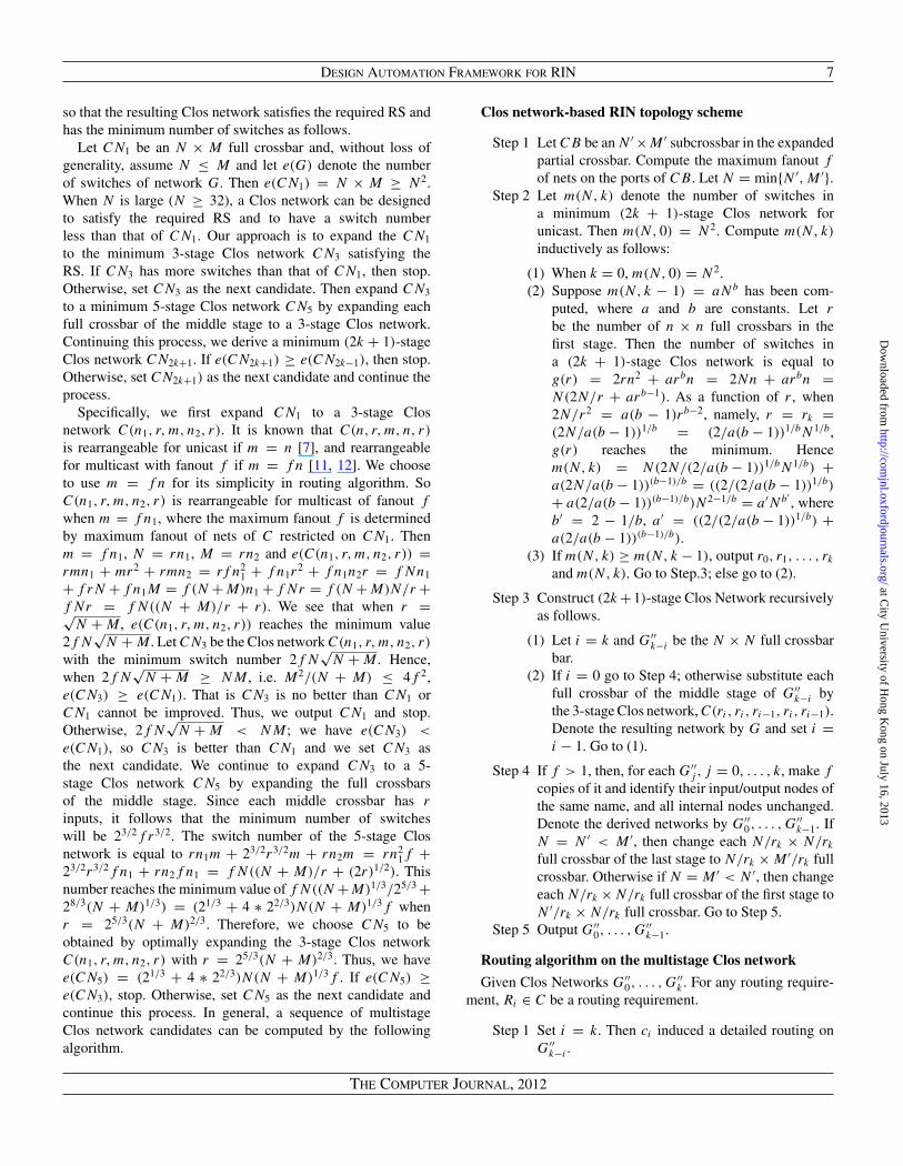
Clos network-based RIN topology scheme
Step 1 Let CB be an N ′ ×M ′ subcrossbar in the expandedpartial crossbar. Compute the maximum fanout f
of nets on the ports of CB. Let N = min{N ′, M ′}.Step 2 Let m(N, k) denote the number of switches in
a minimum (2k + 1)-stage Clos network forunicast. Then m(N, 0) = N2. Compute m(N, k)
inductively as follows:
(1) When k = 0, m(N, 0) = N2.(2) Suppose m(N, k − 1) = aNb has been com-
puted, where a and b are constants. Let r
be the number of n × n full crossbars in thefirst stage. Then the number of switches ina (2k + 1)-stage Clos network is equal tog(r) = 2rn2 + arbn = 2Nn + arbn =N(2N/r + arb−1). As a function of r , when2N/r2 = a(b − 1)rb−2, namely, r = rk =(2N/a(b − 1))1/b = (2/a(b − 1))1/bN1/b,g(r) reaches the minimum. Hencem(N, k) = N(2N/(2/a(b − 1))1/bN1/b) +a(2N/a(b − 1))(b−1)/b = ((2/(2/a(b − 1))1/b)
+ a(2/a(b − 1))(b−1)/b)N2−1/b = a′Nb′, where
b′ = 2 − 1/b, a′ = ((2/(2/a(b − 1))1/b) +a(2/a(b − 1))(b−1)/b).
(3) If m(N, k) ≥ m(N, k − 1), output r0, r1, . . . , rk
and m(N, k). Go to Step.3; else go to (2).
Step 3 Construct (2k +1)-stage Clos Network recursivelyas follows.
(1) Let i = k and G′′k−i be the N × N full crossbar
bar.(2) If i = 0 go to Step 4; otherwise substitute each
full crossbar of the middle stage of G′′k−i by
the 3-stage Clos network, C(ri, ri, ri−1, ri, ri−1).Denote the resulting network by G and set i =i − 1. Go to (1).
Step 4 If f > 1, then, for each G′′j , j = 0, . . . , k, make f
copies of it and identify their input/output nodes ofthe same name, and all internal nodes unchanged.Denote the derived networks by G′′
0, . . . , G′′k−1. If
N = N ′ < M ′, then change each N/rk × N/rk
full crossbar of the last stage to N/rk × M ′/rk fullcrossbar. Otherwise if N = M ′ < N ′, then changeeach N/rk × N/rk full crossbar of the first stage toN ′/rk × N/rk full crossbar. Go to Step 5.
Step 5 Output G′′0, . . . , G
′′k−1.
Routing algorithm on the multistage Clos network
Given Clos Networks G′′0, . . . , G
′′k . For any routing require-
ment, Ri ∈ C be a routing requirement.
Step 1 Set i = k. Then ci induced a detailed routing onG′′
k−i .
The Computer Journal, 2012
at City U
niversity of Hong K
ong on July 16, 2013http://com
jnl.oxfordjournals.org/D
ownloaded from
8 H. Fan et al.
Step 2 If i = 0, then output the derived routing on G′′k−i .
Otherwise, each routing on the middle crossbar ofG′′
k−i corresponds to routing requirements for the3-stage Clos network of the middle three stages.Using the matching algorithm to find a matchingthe middle stage and then expanding to the first andthird stages, we obtain the routing for the middle3-stages of G′′
k−i−1. Set i = i + 1 and go to Step 2.
3.4. Generalized Clos networks
The multicast rearrangeable Clos networks could be badon node cost. For example, the number of intermediatenodes in the broadcast 3-stage (N, N)-Clos network isO(N log N/ log log N) [10]. The intermediate node willincrease fast when the number of stages increases. To avoid thecost explosion of the intermediate nodes, we propose a (2k+1)-stage rearrangeable multicast switching network which uses theminimum number of 2kN intermediate nodes with a trade-offof the switch cost.
The idea is to add more switches to the middle stage of theunicast Clos network so as to increase the routing capacity torearrangeable multicast. It was known that if the middle stagebecomes hyperuniversal [13], then the resulting the 3-stagenetwork is multicast rearrangeable. Thus, we use the followinggeneralized Clos network:
E2(w) = {(p1,j,h, p2,j ′,h′) : |h − h′| ≤ w},Cw(n1, r1, m, n2, r2) = C(n1, r1, m, n2, r2) + E2(w).
(2)
It was proved that when w = 3r1 + 3r2, Cw
(n1, r1, max{n1, n2}, n2, r2) is multicast rearrangeable withthe minimum number of intermediate nodes and theefficient routing algorithm [14]. Therefore, we chooseC3r1+3r2(n1, r1, max{n1, n2}, n2, r2) as an alternative topologycandidate.
Since the middle stage of Cw(n1, r1, max{n1, n2}, n2, r2)
contains max{n1, n2}/w disjoint (wr1, wr2)-full crossbars, wecontinue to expand these full crossbars into 3-stage networks toderive a 5-stage multicast rearrangeable (N, N)-network as thenext candidate for the RIN, and so on by a scheme similar tothe Clos network-based RIN design scheme.
4. DESIGN FOR UNDIRECTED RINS
This section presents a candidate topology design schemefor undirected RS (U, C). This scheme can be appliedto the topology design of custom packet-switchednetwork-on-chip.
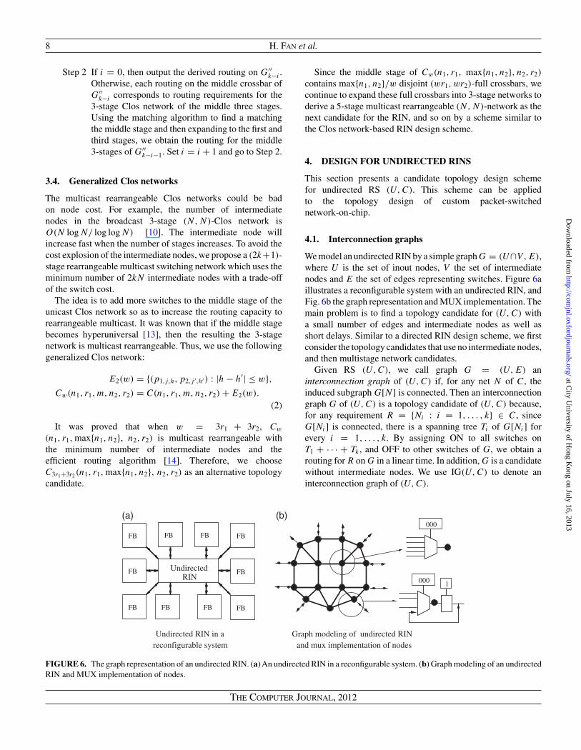
4.1. Interconnection graphs
We model an undirected RIN by a simple graphG = (U∩V, E),where U is the set of inout nodes, V the set of intermediatenodes and E the set of edges representing switches. Figure 6aillustrates a reconfigurable system with an undirected RIN, andFig. 6b the graph representation and MUX implementation. Themain problem is to find a topology candidate for (U, C) witha small number of edges and intermediate nodes as well asshort delays. Similar to a directed RIN design scheme, we firstconsider the topology candidates that use no intermediate nodes,and then multistage network candidates.
Given RS (U, C), we call graph G = (U, E) aninterconnection graph of (U, C) if, for any net N of C, theinduced subgraph G[N ] is connected. Then an interconnectiongraph G of (U, C) is a topology candidate of (U, C) because,for any requirement R = {Ni : i = 1, . . . , k} ∈ C, sinceG[Ni] is connected, there is a spanning tree Ti of G[Ni] forevery i = 1, . . . , k. By assigning ON to all switches onT1 + · · · + Tk , and OFF to other switches of G, we obtain arouting for R on G in a linear time. In addition, G is a candidatewithout intermediate nodes. We use IG(U, C) to denote aninterconnection graph of (U, C).
000
000 1
FB
FB
FB FB FB
UndirectedRIN
FB
FB FB FB FB
reconfigurable systemGraph modeling of undirected RIN
and mux implementation of nodesUndirected RIN in a
(a) (b)
FIGURE 6. The graph representation of an undirected RIN. (a)An undirected RIN in a reconfigurable system. (b) Graph modeling of an undirectedRIN and MUX implementation of nodes.
The Computer Journal, 2012
at City U
niversity of Hong K
ong on July 16, 2013http://com
jnl.oxfordjournals.org/D
ownloaded from
Design Automation Framework for RIN 9
The existence of interconnection graphs is obvious asthe complete graph over U , denoted by IG(U, C), is aninterconnection graph of (U, C). Since IG(U, C) has the fullrouting capacity, we use IG(U, C) as the first candidate.The number of edges in IG(U, C) is O(N2); it may not fit inthe host design, and so next we try to find an IG(U, C) withthe minimum number of edges. Since the problem of findinga minimal interconnection graph is NP-hard [15], we use thegreedy algorithm proposed in to find an IG(U, C), and use it asthe second candidate.
4.2. Multistage switching networks
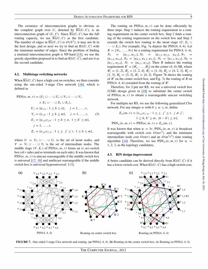
When IG(U, C) have a high cost on switches, we then considerusing the one-sided 3-stage Clos network [16], which isdefined as
PSN(n, m, r) = (U1 ∪ · · · ∪ Ur ∪ V1 ∪ · · · ∪ Vr,
× E1 ∪ · · · ∪ Er ∪ Ec),
Uj = {uj,h : 1 ≤ h ≤ n}, j = 1, . . . , r,
Vj = {vj,h : 1 ≤ h ≤ m}, j = 1, . . . , r,
Ej = {uj,hvj,h′ : 1 ≤ h ≤ n, 1 ≤ h′ ≤ m},j = 1, . . . , r,
Ec = {vj,hvj ′,h : 1 ≤ j, j ′ ≤ r, 1 ≤ h ≤ m},
(3)
where U = U1 ∪ · · · ∪ Ur is the set of inout nodes, andV = V1 ∪ · · · ∪ Vr is the set of intermediate nodes. Themiddle stage (V , Ec) of PSN(n, m, r) forms an (r, m)-switchbox (of r sides and m terminals on each side). It was known thatPSN(n, m, r) is unicast rearrangeable if the middle switch boxis universal [17, 18] and multicast rearrangeable if the middleswitch box is universal hyperuniversal [13].
The routing on PSN(n, m, r) can be done efficiently bythree steps. Step 1 induces the routing requirement to a rout-ing requirement on the center switch box, Step 2 finds a rout-ing of the routing requirement on the switch box and Step 3extends the switch box routing to the inout stage (U, E1 ∪· · · ∪ Er). For example, Fig. 7a depicts the PSN(4, 4, 4). LetR = {N1, . . . , N7} be a routing requirement for PSN(4, 4, 4),N1 = {u1,1, u2,1}, N2 = {u1,2, u2,2, u4,3}, N3 ={u1,4, u4,4}, N4 = {u4,2, u2,3, u3,3}, N5 = {u1,3, u3,2}, N6 ={u3,1, u2,4}, N7 = {u4,1, u3,4}. Then R induces the routingrequirement R′ = {R′
1, . . . , R′7} on the center (4, 4)-SB, where
R′1 = {1, 2}, R′
2 = {1, 2, 4}, R′3 = {1, 4}, R′
4 = {4, 2, 3}, R′5 =
{1, 3}, R′6 = {3, 2}, R′
7 = {4, 3}. Figure 7b shows the routingof R′ on the center switch box, and Fig. 7c the routing of R onPSN(4, 4, 4) extended from the routing of R′.
Therefore, for 2-pin net RS, we use a universal switch box(USB) design given in [18] to substitute the center switchof PSN(n, m, r) to obtain a rearrangeable unicast switchingnetwork.
For multipin net RS, we use the following generalized Closnetwork. For any integer w with 0 ≤ w ≤ m, define
Ew(m, r) = {vj,hvj ′,h′ : 1 ≤ j, j ′ ≤ r, j �= j ′;1 ≤ h, h′ ≤ m, |h − h′| ≤ w},
PSNw(n, m, r) = PSN(n, m, r) + Ew(m, r).
(4)
It was known that when w = 3r , PSNw(n, m, r) is broadcastrearrangeable with switch cost O(mr3), and the minimumintermediate node cost O(mr) and an O(m2r5) time routingalgorithm [14]. Therefore, we use PSNw(n, m, r) for w =1, 2, 3, as the topology candidates.
4.3. RIN design improvement
A better candidate can be derived directly from IG(U, C) if ithas a lower switch cost. When IG(U, C) has a high switch cost,
R’4
R’6
R’7
R’2
R’5
R’3
R’1
R6
1,1
1,2
1,3
2,12,22,32,4
3,2
3,3
3,4
4,1 4,2 4,3 4,4
1,1v
v 1,1
v 2,1v 2,4
3,1v 3,1
v 3,4v 4,1 v 4,4
u
u
u
u
uuuu
u
u
u
u
u u u u
1,4
Routing on PSN(4, 4, 4)
2,12,22,32,4 uuuu
1,1
1,2
3,2
3,3
3,4
4,1 4,2 4,3 4,4
1,1v
v 1,1
v 2,1v 2,4
3,1v 3,1
v 3,4v 4,1 v 4,4
u
u
u
uu
u
u
u
u u u u
1,4
R2
R7 R3
R1
1,3 R5
R4
Routing on center switch boxPSN(4, 4, 4)
(a) (b) (c)
FIGURE 7. One-sided 3-stage Clos network and routing. (a) PSN(4, 4, 4). (b) Routing on the center switch box. (c) Routing on PSN(4, 4, 4).
The Computer Journal, 2012
at City U
niversity of Hong K
ong on July 16, 2013http://com
jnl.oxfordjournals.org/D
ownloaded from
10 H. Fan et al.
we propose to use a network modularity method to find the densemodules of IG(U, C) and then substitute the dense modules byone-sided Clos networks so as to reduce the number of switchesand to preserve the required routing capacity of IG(U, C).
A subgraph H = (V , E) of IG(U, C) is dense if it hasmore than the half of the complete graph on the vertices, i.e.|E| > |V |(|V | − 1)/2 = O(|V |2). By the arguments of theprevious section, when subgraph H is dense, then substitutingthe subgraph by a one-sided rearrangeable multistage switchingnetwork, H ′ will result in a network with a less number ofswitches.
The routing property required on subgraph H = (V , E) canbe preserved as well with the substitution.A routing requirementR ∈ C inducing a routing requirement R[V ] on V . LetC[V ] = {R[V ] : R ∈ C}. Then C[V ] is an induced RS onV . When expanding H to a multistage switching network, wemake the derived switching network routable for C[V ]. Theroutability can be guaranteed by using a one-sided rearrangeableunicast switching network if all requirements in C[V ] are 2-pin net routing requirements with less than O(|V |3/2) switches,otherwise using a one-sided rearrangeable multicast switchingnetwork with O(|V |5/3) switches as described in the previoussection. Therefore, when H is dense, the number of switches canbe reduced by substituting H by a suitable one-sided multistagerearrangeable switching network.
5. CAD TOOLS FOR RIN DESIGN AUTOMATION
We developed a CAD tool for the design automation of a RINbased on the design scheme proposed above. The tool consistsof the following programs.
(1) RS extractor: to determine RS (A, B, U, C).(2) RS simplifier: to produce a set of reduced minimal RSs.(3) RIN topology generator: given directed RS
(A, B, U, C), to generate a sequence of topologycandidates.
(4) RIN circuit generator: given a RIN topology graph(either directed or undirected), to generate the circuitin Verilog HDL format.
(5) Control circuit generator: to generate control circuits forRINs.
(6) Router: to find routing for a given routing requirement.(7) Configuration bit generator: to convert the routing to a
configuration bit stream.
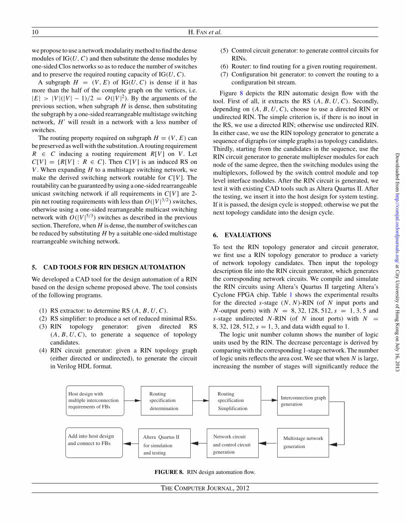
Figure 8 depicts the RIN automatic design flow with thetool. First of all, it extracts the RS (A, B, U, C). Secondly,depending on (A, B, U, C), choose to use a directed RIN orundirected RIN. The simple criterion is, if there is no inout inthe RS, we use a directed RIN; otherwise use undirected RIN.In either case, we use the RIN topology generator to generate asequence of digraphs (or simple graphs) as topology candidates.Thirdly, starting from the candidates in the sequence, use theRIN circuit generator to generate multiplexer modules for eachnode of the same degree, then the switching modules using themultiplexors, followed by the switch control module and toplevel interface modules. After the RIN circuit is generated, wetest it with existing CAD tools such as Altera Quartus II. Afterthe testing, we insert it into the host design for system testing.If it is passed, the design cycle is stopped; otherwise we put thenext topology candidate into the design cycle.
6. EVALUATIONS
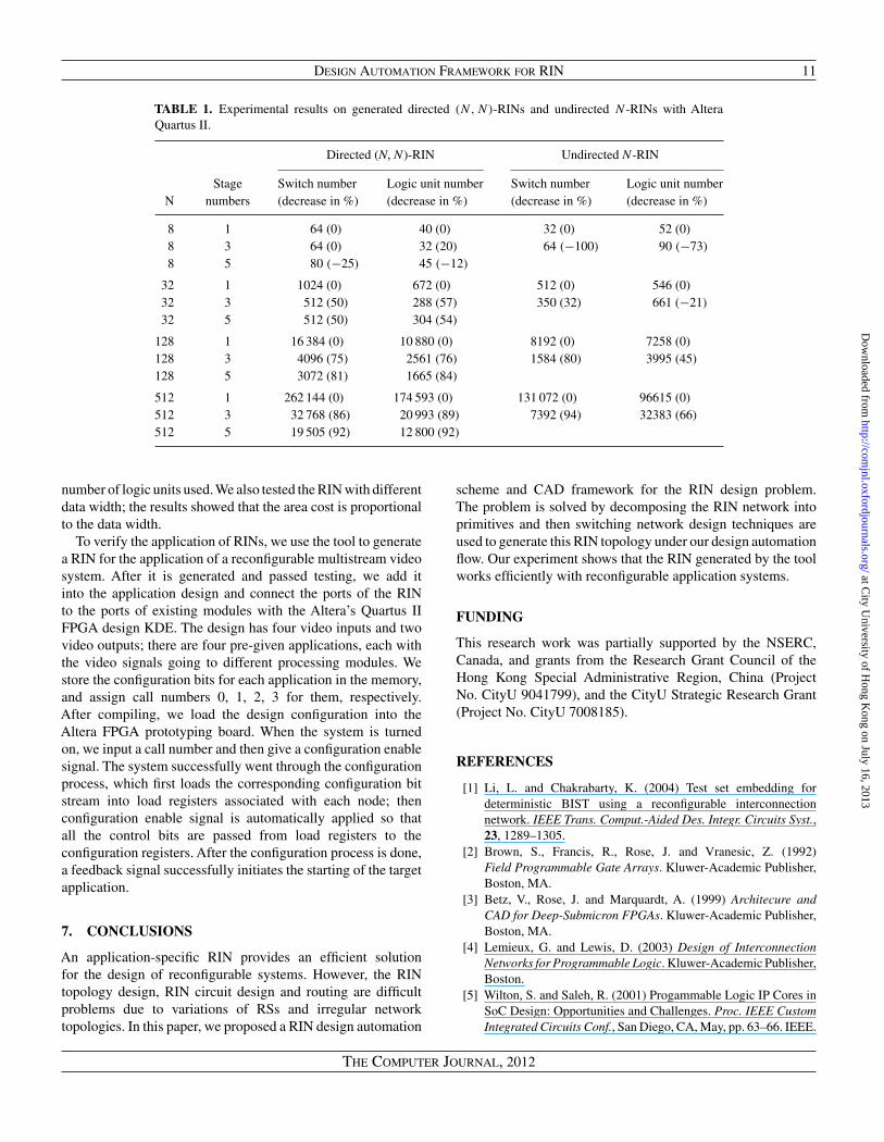
To test the RIN topology generator and circuit generator,we first use a RIN topology generator to produce a varietyof network topology candidates. Then input the topologydescription file into the RIN circuit generator, which generatesthe corresponding network circuits. We compile and simulatethe RIN circuits using Altera’s Quartus II targeting Altera’sCyclone FPGA chip. Table 1 shows the experimental resultsfor the directed s-stage (N, N)-RIN (of N input ports andN -output ports) with N = 8, 32, 128, 512, s = 1, 3, 5 ands-stage undirected N -RIN (of N inout ports) with N =8, 32, 128, 512, s = 1, 3, and data width equal to 1.
The logic unit number column shows the number of logicunits used by the RIN. The decrease percentage is derived bycomparing with the corresponding 1-stage network. The numberof logic units reflects the area cost. We see that when N is large,increasing the number of stages will significantly reduce the
specificationRouting
Simplification
specificationRouting
determination
Host design withmultiple interconnectionrequirements of FBs
Altera Quartus II
for simulation
and testing
Add into host designand connect to FBs
Interconnection graph
Multistage network
generation
generation
Network circuit
and control circuit
generation
FIGURE 8. RIN design automation flow.
The Computer Journal, 2012
at City U
niversity of Hong K
ong on July 16, 2013http://com
jnl.oxfordjournals.org/D
ownloaded from
Design Automation Framework for RIN 11
TABLE 1. Experimental results on generated directed (N, N)-RINs and undirected N -RINs with AlteraQuartus II.
Directed (N, N)-RIN Undirected N-RIN
Stage Switch number Logic unit number Switch number Logic unit numberN numbers (decrease in %) (decrease in %) (decrease in %) (decrease in %)
8 1 64 (0) 40 (0) 32 (0) 52 (0)8 3 64 (0) 32 (20) 64 (−100) 90 (−73)
8 5 80 (−25) 45 (−12)
32 1 1024 (0) 672 (0) 512 (0) 546 (0)32 3 512 (50) 288 (57) 350 (32) 661 (−21)
32 5 512 (50) 304 (54)
128 1 16 384 (0) 10 880 (0) 8192 (0) 7258 (0)128 3 4096 (75) 2561 (76) 1584 (80) 3995 (45)128 5 3072 (81) 1665 (84)
512 1 262 144 (0) 174 593 (0) 131 072 (0) 96615 (0)512 3 32 768 (86) 20 993 (89) 7392 (94) 32383 (66)512 5 19 505 (92) 12 800 (92)
number of logic units used. We also tested the RIN with differentdata width; the results showed that the area cost is proportionalto the data width.
To verify the application of RINs, we use the tool to generatea RIN for the application of a reconfigurable multistream videosystem. After it is generated and passed testing, we add itinto the application design and connect the ports of the RINto the ports of existing modules with the Altera’s Quartus IIFPGA design KDE. The design has four video inputs and twovideo outputs; there are four pre-given applications, each withthe video signals going to different processing modules. Westore the configuration bits for each application in the memory,and assign call numbers 0, 1, 2, 3 for them, respectively.After compiling, we load the design configuration into theAltera FPGA prototyping board. When the system is turnedon, we input a call number and then give a configuration enablesignal. The system successfully went through the configurationprocess, which first loads the corresponding configuration bitstream into load registers associated with each node; thenconfiguration enable signal is automatically applied so thatall the control bits are passed from load registers to theconfiguration registers. After the configuration process is done,a feedback signal successfully initiates the starting of the targetapplication.
7. CONCLUSIONS
An application-specific RIN provides an efficient solutionfor the design of reconfigurable systems. However, the RINtopology design, RIN circuit design and routing are difficultproblems due to variations of RSs and irregular networktopologies. In this paper, we proposed a RIN design automation
scheme and CAD framework for the RIN design problem.The problem is solved by decomposing the RIN network intoprimitives and then switching network design techniques areused to generate this RIN topology under our design automationflow. Our experiment shows that the RIN generated by the toolworks efficiently with reconfigurable application systems.
FUNDING
This research work was partially supported by the NSERC,Canada, and grants from the Research Grant Council of theHong Kong Special Administrative Region, China (ProjectNo. CityU 9041799), and the CityU Strategic Research Grant(Project No. CityU 7008185).
REFERENCES
[1] Li, L. and Chakrabarty, K. (2004) Test set embedding fordeterministic BIST using a reconfigurable interconnectionnetwork. IEEE Trans. Comput.-Aided Des. Integr. Circuits Syst.,23, 1289–1305.
[2] Brown, S., Francis, R., Rose, J. and Vranesic, Z. (1992)Field Programmable Gate Arrays. Kluwer-Academic Publisher,Boston, MA.
[3] Betz, V., Rose, J. and Marquardt, A. (1999) Architecure andCAD for Deep-Submicron FPGAs. Kluwer-Academic Publisher,Boston, MA.
[4] Lemieux, G. and Lewis, D. (2003) Design of InterconnectionNetworks for Programmable Logic. Kluwer-Academic Publisher,Boston.
[5] Wilton, S. and Saleh, R. (2001) Progammable Logic IP Cores inSoC Design: Opportunities and Challenges. Proc. IEEE CustomIntegrated Circuits Conf., San Diego, CA, May, pp. 63–66. IEEE.
The Computer Journal, 2012
at City U
niversity of Hong K
ong on July 16, 2013http://com
jnl.oxfordjournals.org/D
ownloaded from

12 H. Fan et al.
[6] Parvez, H., Marrakchi, Z. and Mehrez, H. (2010) ApplicationSpecific FPGA Using Heterogeneous Logic Blocks. Int.Symposium on Reconfigurable Computing: Architectures, Toolsand Applications, Milano, Italy, pp. 92–109. Springer.
[7] Clos, C. (1953) A Study of Nonblocking Switching Networks.Bell Syst Tech. J., 22, 406–424.
[8] Hawang, F.K. (2004) The Mathematical Theory of NonblockingSwitching Networks (Series on Applied Mathematics). WorldScientific Publishing Co., Inc., River Edge, NJ, USA.
[9] Dolev, D., Dwork, C., Pippenger, N. and Wigderson, A. (1983)Superconcentrators, Generalizers and Generalized Connectorswith Limited Depth (Preliminary Version). ACM Symposium onTheory of Computing, pp. 42–51. ACM.
[10] Yang, Y. and Masson, G.M. (1991) Nonblocking broadcastswitching networks. IEEE Trans. Comput., 40, 1005–1015.
[11] Masson, G.M. and Jordan, B.W. (1972) Generalized multi-stageconnection networks. Networks, 2, 191–209.
[12] Hwang, F.K. (1972) Rearrangeahility of multiconnection three-stage networks. Networks, 2, 301–306.
[13] Fan, H., Liu, J., Wu, Y.L. and Cheung, C.C. (2003) On optimalhyper universal and rearrageable switch box designs. IEEE Trans.Comput. Aided Des., 22, 1637–1649.
[14] Fan, H. and Wu,Y.-L. (2009) A New Approach for RearrangeableMulticast Switching Networks. Int. Conf., CombinatorialOptimization and Applications, Thailand, pp. 384–394. Springer.
[15] Fan, H., Hundt, C., Wu, Y.-L. and Ernst, J. (2008) Algorithmsand Implementation for Interconnection Graph Problem.Int. Conf., Combinatorial Optimization and Applications,pp. 201–210. Springer, St. John’s, NL, Canada.
[16] Yen, M., Chen, S. and Lan, S. (2001) A three-stage one-sided rearrangeable polygonal switching network. IEEE Trans.Comput., 50, 1291–1294.
[17] Chang,Y.W.,Wong, D.F. andWong, C.K. (1996) Universal switchmodules for FPGA design. ACM Trans. Des. Autom. Electron.Syst., 1, 80–101.
[18] Shyu, M., Wu, G.M., Chang, Y.D. and Chang, Y.W. (2000)Generic universal switch blocks. IEEE Trans. Comput., 49,348–359.
The Computer Journal, 2012
at City U
niversity of Hong K
ong on July 16, 2013http://com
jnl.oxfordjournals.org/D
ownloaded from