4 Processor and Intel - DigChip
380
Pentium ® 4 Processor and Intel ® 852GME Chipset Platform Design Guide September 2006 Order Number: 273935-002
-
Upload
khangminh22 -
Category
Documents
-
view
0 -
download
0
Transcript of 4 Processor and Intel - DigChip

Pentium® 4 Processor and Intel® 852GME Chipset PlatformDesign Guide
September 2006
Order Number: 273935-002

2 Design Guide
Pentium® 4 Processor and Intel® 852GME Chipset Platform
INFORMATION IN THIS DOCUMENT IS PROVIDED IN CONNECTION WITH INTEL® PRODUCTS. NO LICENSE, EXPRESS OR IMPLIED, BY ESTOPPEL OR OTHERWISE, TO ANY INTELLECTUAL PROPERTY RIGHTS IS GRANTED BY THIS DOCUMENT. EXCEPT AS PROVIDED IN INTEL'S TERMS AND CONDITIONS OF SALE FOR SUCH PRODUCTS, INTEL ASSUMES NO LIABILITY WHATSOEVER, AND INTEL DISCLAIMS ANY EXPRESS OR IMPLIED WARRANTY, RELATING TO SALE AND/OR USE OF INTEL PRODUCTS INCLUDING LIABILITY OR WARRANTIES RELATING TO FITNESS FOR A PARTICULAR PURPOSE, MERCHANTABILITY, OR INFRINGEMENT OF ANY PATENT, COPYRIGHT OR OTHER INTELLECTUAL PROPERTY RIGHT. Intel products are not intended for use in medical, life saving, life sustaining, critical control or safety systems, or in nuclear facility applications.
Intel may make changes to specifications and product descriptions at any time, without notice.
The Intel product(s) referred to in this document are intended for standard commercial use only. Customer is solely responsible for assessing the suitability of the product(s) for use in particular applications.
Designers must not rely on the absence or characteristics of any features or instructions marked “reserved” or “undefined.” Intel reserves these for future definition and should have no responsibility whatsoever for conflicts or incompatibilities arising from future changes to them.
The Pentium® 4 Processor and Intel® 852GME Chipset Platform may contain design defects or errors known as errata which may cause the product to deviate from published specifications. Current characterized errata are available on request.
This document and the software described in it are furnished under license and may only be used or copied in accordance with the terms of the license. The information in this document is furnished for informational use only, is subject to change without notice, and should not be construed as a commitment by Intel Corporation. Intel Corporation assumes no responsibility or liability for any errors or inaccuracies that may appear in this document or any software that may be provided in association with this document. Except as permitted by such license, no part of this document may be reproduced, stored in a retrieval system, or transmitted in any form or by any means without the express written consent of Intel Corporation.
Performance tests and ratings are measured using specific computer systems and/or components and reflect the approximate performance of Intel products as measured by those tests. Any difference in system hardware or software design or configuration may affect actual performance. Buyers should consult other sources of information to evaluate the performance of systems or components they are considering purchasing. For more information on performance tests and on the performance of Intel products, reference www.intel.com or call (U.S.) 1-800-628-8686 or 1-916-356-3104.
Contact your local Intel sales office or your distributor to obtain the latest specifications and before placing your product order.
Copies of documents which have an ordering number and are referenced in this document, or other Intel literature may be obtained by calling 1-800-548-4725 or by visiting Intel's website at http://www.intel.com.
Celeron, Intel, Intel logo, Intel NetBurst, Intel SpeedStep, and Pentium are trademarks or registered trademarks of Intel Corporation or its subsidiaries in the United States and other countries.
*Other names and brands may be claimed as the property of others.
Third party vendors or devices are listed by Intel as a convenience to Intel's general customer base, but Intel does not make any representations or warranties whatsoever regarding quality, reliability, functionality or compatibility of these devices. This list and/or these devices may be subject to change without notice.
Copyright © Intel Corporation, 2006

Design Guide 3
Pentium® 4 Processor and Intel® 852GME Chipset PlatformContents
Contents1 Introduction..................................................................................................................................19
1.1 Conventions and Terminology ............................................................................................191.2 Reference Documents ........................................................................................................21
2 System Overview .........................................................................................................................23
2.1 System Features.................................................................................................................232.2 Pentium® 4 Processor ........................................................................................................25
2.2.1 Architectural Features............................................................................................252.2.2 Packaging/Power...................................................................................................25
2.3 Intel® 852GME Chipset Graphics Memory Controller Hub (GMCH)...................................252.3.1 Multiplexed AGP and Intel® DVO Interface ...........................................................252.3.2 Accelerated Graphics Port (AGP) Interface ...........................................................252.3.3 Integrated System Memory DRAM Controller........................................................262.3.4 Internal Graphics Controller ...................................................................................26
2.4 Package/Power...................................................................................................................272.4.1 Intel® 82801DB I/O Controller Hub (ICH4) ............................................................27
2.4.1.1 Packaging/Power ...................................................................................272.4.2 Firmware Hub (FWH).............................................................................................28
2.4.2.1 Packaging/Power ...................................................................................28
3 General Design Considerations .................................................................................................29
3.1 Recommended Board Stack-Up .........................................................................................293.2 Alternate Stack-Ups............................................................................................................31
4 Platform Power Requirements ...................................................................................................33
4.1 Introduction .........................................................................................................................334.1.1 Power Delivery Architectural Block Diagram .........................................................334.1.2 Processor Phase Lock Loop Design Guidelines....................................................34
4.1.2.1 Other Recommendations .......................................................................354.1.3 Voltage and Current...............................................................................................364.1.4 Voltage Identification for VRM/EVRD 10.0 ............................................................374.1.5 VCC_CORE Power Sequencing............................................................................394.1.6 Voltage Regulator Design Recommendations .......................................................394.1.7 Decoupling Requirements .....................................................................................404.1.8 Layout ....................................................................................................................424.1.9 Thermal Considerations.........................................................................................464.1.10 Simulation ..............................................................................................................47
5 Integrated Graphics Display Port...............................................................................................49
5.1 Analog RGB/CRT Guidelines .............................................................................................495.1.1 RAMDAC/Display Interface....................................................................................495.1.2 Reference Resistor (REFSET)...............................................................................495.1.3 RAMDAC Board Design Guidelines.......................................................................505.1.4 Intel® 852GME Chipset DAC Routing Guidelines..................................................515.1.5 DAC Power Requirements.....................................................................................535.1.6 HSYNC and VSYNC Design Considerations.........................................................545.1.7 DDC and I2C Design Considerations.....................................................................54

4 Design Guide
Pentium® 4 Processor and Intel® 852GME Chipset Platform Contents
5.2 LVDS Transmitter Interface ................................................................................................ 545.2.1 Length Matching Constraints ................................................................................. 55
5.2.1.1 LVDS Package Length Compensation .................................................. 555.2.2 LVDS Routing Guidelines...................................................................................... 56
5.3 Digital Video Out Port ......................................................................................................... 585.3.1 DVO Interface Signal Groups ................................................................................ 58
5.3.1.1 DVOB Interface Signals ......................................................................... 585.3.1.2 DVOC Interface Signals......................................................................... 585.3.1.3 Common Signals for Both DVO Ports.................................................... 59
5.3.2 DVOB and DVOC Port Interface Routing Guidelines ............................................595.3.2.1 Length Mismatch Requirements ............................................................ 595.3.2.2 Package Length Compensation............................................................. 605.3.2.3 DVOB and DVOC Routing Guidelines ................................................... 605.3.2.4 DVOB and DVOC Port Termination....................................................... 62
5.3.3 DVOB and DVOC Assumptions, Definitions, and Specifications........................... 625.3.4 DVOB and DVOC Simulation Method ................................................................... 63
5.4 DVOB and DVOC Port Flexible (Modular) Design.............................................................. 645.4.1 DVOB and DVOC Module Design ......................................................................... 64
5.4.1.1 Generic Connector Model ......................................................................655.5 DVO GMBUS and DDC Interface Considerations.............................................................. 65
5.5.1 Leaving the GMCH DVOB or DVOC Port Unconnected........................................ 665.6 Miscellaneous Input Signals and Voltage Reference ......................................................... 67
6 System Memory Design Guidelines........................................................................................... 69
6.1 Introduction......................................................................................................................... 696.2 Length Matching and Length Formulas .............................................................................. 706.3 Package Length Compensation.......................................................................................... 706.4 Topologies and Routing Guidelines.................................................................................... 71
6.4.1 Clock Signals – SCK[5:0], SCK[5:0]# ....................................................................716.4.2 Clock Topology Diagram .......................................................................................726.4.3 DDR Clock Routing Guidelines.............................................................................. 72
6.4.3.1 Clock Length Matching Requirements ................................................... 746.4.3.2 Clock Reference Lengths....................................................................... 746.4.3.3 Clock Length Package Table ................................................................. 76
6.4.4 Data Signals – SDQ[71:0], SDM[8:0], SDQS[8:0] .................................................766.4.4.1 Data Bus Topology ................................................................................ 776.4.4.2 SDQS to Clock Length Matching Requirements.................................... 796.4.4.3 Data to Strobe Length Matching Requirements.....................................806.4.4.4 SDQ to SDQS Mapping ......................................................................... 816.4.4.5 SDQ/SDQS Signal Package Lengths .................................................... 836.4.4.6 Memory Data Routing Example ............................................................. 85
6.4.5 Control Signals – SCKE[3:0], SCS[3:0]# ...............................................................856.4.5.1 Control Signal Topology......................................................................... 866.4.5.2 Control Signal Routing Guidelines ......................................................... 876.4.5.3 Control to Clock Length Matching Requirements .................................. 886.4.5.4 Control Group Package Length Table ................................................... 906.4.5.5 Control Topology Routing Example ....................................................... 91
6.4.6 Command Signals – SMA[12:6,3,0], SBA[1:0], SRAS#, SCAS#, SWE#............... 916.4.6.1 Command Topology Routing Guidelines ............................................... 936.4.6.2 Command Topology Length Matching Requirements............................ 946.4.6.3 Command Group Package Length Table .............................................. 966.4.6.4 Command Topology Routing Example .................................................. 97

Design Guide 5
Pentium® 4 Processor and Intel® 852GME Chipset PlatformContents
6.4.7 CPC Signals – SMA[5,4,2,1], SMAB[5,4,2,1] ........................................................976.4.7.1 CPC Signal Topology.............................................................................986.4.7.2 CPC Signal Routing Guidelines .............................................................996.4.7.3 CPC to Clock Length Matching Requirements ....................................1006.4.7.4 CPC Group Package Length Table .....................................................102
6.4.8 Feedback – RCVENOUT#, RCVENIN#...............................................................1026.5 ECC Guidelines ................................................................................................................102
6.5.1 Graphics Limitations Using ECC Memory............................................................1026.5.2 GMCH ECC Functionality ....................................................................................1036.5.3 DRAM Clock Flexibility.........................................................................................104
7 Miscellaneous Logic .................................................................................................................105
7.1 Glue Chip 4.......................................................................................................................1057.2 Discrete Logic ...................................................................................................................106
8 Front Side Bus Design Guidelines...........................................................................................107
8.1 FSB Routing Guidelines ...................................................................................................1078.1.1 Return Path Evaluation ........................................................................................109
8.2 OPTIMIZED/COMPAT# Topology for Intel® 852GME Platforms......................................1098.2.1 GTLREF Layout and Routing Recommendations................................................110
8.3 Processor Configuration ...................................................................................................1108.4 General Topology and Layout Guidelines ........................................................................111
8.4.1 Design Recommendations...................................................................................1118.4.1.1 Data .....................................................................................................1118.4.1.2 Address................................................................................................1118.4.1.3 Strobe ..................................................................................................1118.4.1.4 Common Clock ....................................................................................111
8.4.2 Source Synchronous (SS) Signals ......................................................................1128.4.3 Common Clock (CC) AGTL+ Signals ..................................................................1138.4.4 Asynchronous AGTL+ and Other Signals ............................................................114
8.4.4.1 Topology 1A: Asynchronous GTL+ Signal Driven by the Processor—IERR# and FERR#114
8.4.4.2 Topology 1B: Asynchronous GTL+ Signal Driven by the Processor—PROCHOT#115
8.4.4.3 Topology 1C: Asynchronous GTL+ Signal Driven by the Processor—THERMTRIP#116
8.4.4.4 Topology 2A: Asynchronous GTL+ Signals Driven by theIntel® 82801DB ICH4—A20M#, IGNNE#, LINT[1:0], SLP#,SMI#, and STPCLK#117
8.4.4.5 Topology 2B: Asynchronous GTL+ Signal Driven by theIntel® 82801DB ICH4—INIT#118
8.4.4.6 Topology 2C: Miscellaneous Signal Drivenby the Intel® 82801DB ICH4 Open Drain—PWRGOOD......................119
8.4.4.7 Topology 3: VCCIOPLL, VCCA and VSSA..........................................1198.4.4.8 Topology 4: BR0# and RESET# ..........................................................1198.4.4.9 Topology 5: COMP[1:0] Signals...........................................................1208.4.4.10 Topology 6: THERMDA/THERMDC Routing Guidelines .....................1208.4.4.11 Topology 7: TESTHI Pins ....................................................................120
8.5 Additional Processor Design Considerations....................................................................1218.5.1 Retention Mechanism Placement and Keepouts.................................................1218.5.2 Power Header for Active Cooling Solutions .........................................................124
8.6 Debug Port Routing Guidelines ........................................................................................124

6 Design Guide
Pentium® 4 Processor and Intel® 852GME Chipset Platform Contents
8.6.1 Debug Tools Specifications ................................................................................. 1248.6.1.1 Logic Analyzer Interface (LAI).............................................................. 1248.6.1.2 Mechanical Considerations..................................................................1258.6.1.3 Electrical Considerations ..................................................................... 125
8.7 Pentium® 4 Processor and Intel® 852GME Chipset FSB Signal Package Lengths .........126
9 Hub Interface.............................................................................................................................. 131
9.1 Hub Interface Compensation ............................................................................................1319.2 Hub Interface Data HL[10:0] and Strobe Signals.............................................................. 132
9.2.1 HL[10:0] and Strobe Signals Internal Layer Routing ........................................... 1329.2.2 ICH4 Strobe Signal Pin Map Change ..................................................................133
9.3 Hub VREF/VSWING Generation/Distribution ................................................................... 1339.3.1 Single Generation Reference Voltage Divider Circuit..........................................1349.3.2 Locally Generated Reference Voltage Divider Circuit ......................................... 135
9.3.2.1 ICH4 Single Generated Voltage Reference Divider Circuit.................. 1359.3.2.2 GMCH Single Generated Voltage Reference Divider Circuit............... 136
9.3.3 Separate GMCH and ICH4 Voltage Divider Circuits for VREF and VSWING ..... 1379.3.3.1 Separate ICH4 Voltage Divider Circuits for HIVREF and HI_VSWING1379.3.3.2 Separate GMCH Voltage Divider Circuits for HLVREF and PSWING .138
9.4 Hub Interface Decoupling Guidelines ............................................................................... 138
10 AGP Port Design Guidelines .................................................................................................... 139
10.1 AGP Interface ................................................................................................................... 13910.2 AGP 2.0 Specification....................................................................................................... 140
10.2.1 AGP 2.0 ...............................................................................................................14010.2.2 AGP Interface Signal Groups .............................................................................. 140
10.3 AGP Routing Guidelines...................................................................................................14210.3.1 1x Timing Domain Routing Guidelines ................................................................ 142
10.3.1.1 Trace Length Requirements for AGP 1X ............................................. 14210.3.1.2 Trace Spacing Requirements .............................................................. 14210.3.1.3 Trace Length Mismatch ....................................................................... 142
10.3.2 2x/4x Timing Domain Routing Guidelines............................................................ 14310.3.2.1 Trace Length Requirements for AGP 2X/4X........................................14310.3.2.2 Trace Spacing Requirements .............................................................. 14310.3.2.3 Trace Length Mismatch Requirements ................................................ 144
10.3.3 AGP Clock Skew ................................................................................................. 14510.3.4 AGP Signal Noise Decoupling Guidelines ........................................................... 14510.3.5 AGP Interface Package Lengths .........................................................................14610.3.6 AGP Routing Ground Reference .........................................................................14710.3.7 Pull-Ups ...............................................................................................................14810.3.8 AGP VDDQ and VREF ........................................................................................ 15010.3.9 VREF Generation for AGP 2.0 (2X and 4X) ........................................................ 150
10.3.9.1 1.5 Volt AGP Interface (2X/4X) ............................................................ 15010.3.10 AGP Compensation ............................................................................................. 15010.3.11 AGP Reference Information................................................................................. 150
11 I/O Subsystem............................................................................................................................ 151
11.1 SYS_RESET# Usage Model ............................................................................................15111.2 PWRBTN# Usage Model.................................................................................................. 15111.3 Power Well Isolation Control Strap Requirements............................................................ 15211.4 IDE Interface..................................................................................................................... 152
Design Guide 7
Pentium® 4 Processor and Intel® 852GME Chipset PlatformContents
11.4.1 Cabling.................................................................................................................15311.4.1.1 Cable Detection for Ultra ATA 66 and Ultra ATA100 ...........................15311.4.1.2 Combination Host Side/Device Side Cable Detection .........................15411.4.1.3 Device Side Cable Detection ...............................................................155
11.4.2 Primary IDE Connector Requirements.................................................................15611.4.3 Secondary IDE Connector Requirements............................................................157
11.5 PCI....................................................................................................................................15811.5.1 PCI Routing Summary .........................................................................................158
11.6 AC’97 ................................................................................................................................16011.6.1 AC’97 Routing......................................................................................................16311.6.2 Motherboard Implementation ...............................................................................164
11.6.2.1 Valid Codec Configurations .................................................................16411.6.3 SPKR Pin Configuration ......................................................................................165
11.7 CNR ..................................................................................................................................16511.7.1 AC’97 Audio Codec Detect Circuit and Configuration Options ............................16611.7.2 CNR 1.2 AC’97 Disable and Demotion Rules for the Motherboard .....................16611.7.3 CNR Routing Summary .......................................................................................168
11.8 USB 2.0 Guidelines and Recommendations ....................................................................16811.8.1 Layout Guidelines ................................................................................................168
11.8.1.1 General Routing and Placement ..........................................................16811.8.1.2 USB 2.0 Trace Separation ...................................................................16911.8.1.3 USBRBIAS Connection........................................................................17011.8.1.4 USB 2.0 Termination............................................................................17011.8.1.5 USB 2.0 Trace Length Pair Matching ..................................................17011.8.1.6 USB 2.0 Trace Length Guidelines .......................................................171
11.8.2 Plane Splits, Voids, and Cut-Outs (Anti-Etch)......................................................17111.8.2.1 VCC Plane Splits, Voids, and Cut-Outs (Anti-Etch) ..............................17111.8.2.2 Ground Plane Splits, Voids, and Cut-Outs (Anti-Etch).........................172
11.8.3 USB Power Line Layout Topology .......................................................................17211.8.4 EMI Considerations .............................................................................................17311.8.5 ESD .....................................................................................................................174
11.9 Front Panel Solutions .......................................................................................................17411.9.1 Internal USB Cables ............................................................................................174
11.9.1.1 Internal Cable Option 1 ........................................................................17411.9.1.2 Internal Cable Option 2 ........................................................................17411.9.1.3 Motherboard/PCB Mating Connector ...................................................17511.9.1.4 Routing Considerations........................................................................17711.9.1.5 Front Panel Connector Card ................................................................17711.9.1.6 Front Panel Daughter Card Design Guidelines....................................177
11.10 IOAPIC (I/O Advanced Programmable Interrupt Controller) .............................................17811.10.1 IOAPIC Disabling Options (Recommended Implementation) ..............................17811.10.2 PIRQ Routing Example........................................................................................179
11.11 SMBus 2.0/SMLink Interface ............................................................................................18011.11.1 SMBus Architecture and Design Considerations .................................................181
11.11.1.1 SMBus Design Considerations ............................................................18111.11.1.2 General Design Issues/Notes ..............................................................181
11.11.2 Power Supply Considerations..............................................................................18211.11.2.1 Unified VCC_ Suspend Architecture .....................................................18211.11.2.2 Device Class Considerations ...............................................................183
11.12 FWH..................................................................................................................................18411.12.1 FWH Decoupling..................................................................................................184

8 Design Guide
Pentium® 4 Processor and Intel® 852GME Chipset Platform Contents
11.12.2 In-circuit FWH Programming ............................................................................... 18411.12.3 FWH INIT# Voltage Compatibility ........................................................................ 18411.12.4 FWH VPP Design Guidelines .............................................................................. 184
11.13 RTC ..................................................................................................................................18511.13.1 RTC Crystal ......................................................................................................... 18611.13.2 External Capacitors ............................................................................................. 18711.13.3 RTC Layout Considerations................................................................................. 18811.13.4 RTC External Battery Connections...................................................................... 18811.13.5 RTC External RTCRST# Circuit .......................................................................... 19011.13.6 VBIAS DC Voltage and Noise Measurements..................................................... 19011.13.7 SUSCLK .............................................................................................................. 19111.13.8 RTC-Well Input Strap Requirements ................................................................... 191
11.14 Internal LAN Layout Guidelines........................................................................................ 19111.14.1 Intel® 82801DB ICH4 – LAN Connect Interface Guidelines ................................ 192
11.14.1.1 Bus Topologies .................................................................................... 19211.14.1.2 Signal Routing and Layout................................................................... 19411.14.1.3 Crosstalk Consideration....................................................................... 19511.14.1.4 Impedances ......................................................................................... 19511.14.1.5 Line Termination .................................................................................. 19511.14.1.6 Disabling the Intel® 82801DB ICH4 Integrated LAN............................195
11.14.2 Intel® 82562EM/Intel® 82562ET Platform LAN Connect Component Guidelines19511.14.2.1 Guidelines for Intel® 82562EM/Intel® 82562ET Platform LAN
Connect Component Placement .......................................................... 19511.14.2.2 Crystals and Oscillators ....................................................................... 19611.14.2.3 Intel® 82562ET/Intel® 82562EM Platform LAN Connect
Component Termination Resistors ......................................................19611.14.2.4 Critical Dimensions .............................................................................. 19711.14.2.5 Reducing Circuit Inductance ................................................................ 198
11.14.3 Intel® 82562EM/Intel® ET Platform LAN ConnectComponent Disable Guidelines ........................................................................... 199
11.14.4 General Intel® 82562EM/Intel® 82562ET DifferentialPair Trace Routing Considerations...................................................................... 20011.14.4.1 Trace Geometry and Length ................................................................ 20111.14.4.2 Signal Isolation.....................................................................................20111.14.4.3 Magnetics Module General Power and Ground Plane Considerations 20211.14.4.4 Common Physical Layout Issues......................................................... 203
11.15 GPIO................................................................................................................................. 204
12 Platform Clock Routing Guidelines ......................................................................................... 207
12.1 System Clock Groups....................................................................................................... 20712.2 Clock Group Topologies and Routing Constraints............................................................ 209
12.2.1 Host Clock Group ................................................................................................ 20912.2.1.1 Host Clock Group General Routing Guidelines ...................................21112.2.1.2 EMI Constraints ................................................................................... 211
12.2.2 CLK66 Clock Group............................................................................................. 21212.2.3 CLK33 Clock Group............................................................................................. 21312.2.4 PCI Clock Group.................................................................................................. 21412.2.5 CLK14 Clock Group............................................................................................. 21512.2.6 DOTCLK Clock Group ......................................................................................... 21612.2.7 SSCCLK Clock Group ......................................................................................... 21712.2.8 USBCLK Clock Group ......................................................................................... 218
12.3 CK-408 PWRDWN# Signal Connections.......................................................................... 219

Design Guide 9
Pentium® 4 Processor and Intel® 852GME Chipset PlatformContents
13 Intel® 852GME Chipset Platform Power Delivery Guidelines ................................................221
13.1 Definitions .........................................................................................................................22113.2 Power Delivery Map..........................................................................................................22213.3 GMCH/Intel® 82801DB ICH4 Platform Power-Up Sequence ...........................................224
13.3.1 ICH4 Power Sequencing Requirements ..............................................................22613.3.1.1 3.3/1.5 V Power Sequencing ...............................................................22613.3.1.2 V5REF/ V5REFSUS Sequencing ........................................................22713.3.1.3 Power Supply PS_ON Consideration ..................................................227
13.3.2 GMCH Power Sequencing Requirements ...........................................................22813.3.3 DDR Memory Power Sequencing Requirements.................................................228
13.3.3.1 VTT Rail Power Down Sequencing During Suspend ...........................22813.3.3.2 VTT Rail Power Up Sequencing During Resume ................................229
13.4 Intel® 852GME Chipset Platform Power Delivery Guidelines ...........................................22913.4.1 Pentium® 4 Processor Decoupling Guidelines ....................................................22913.4.2 Intel® 82852GME GMCH Decoupling Guidelines................................................23013.4.3 GMCH VCCSM Decoupling..................................................................................23113.4.4 DDR SDRAM VDD Decoupling............................................................................23113.4.5 DDR VTT Decoupling Placement and Layout Guidelines....................................23113.4.6 DDR Power Delivery Design Guidelines..............................................................232
13.4.6.1 2.5 V Power Delivery Guidelines .........................................................23213.4.6.2 GMCH and DDR SMVREF Design Recommendations .......................23513.4.6.3 DDR SMRCOMP Resistive Compensation..........................................23513.4.6.4 DDR VTT Termination .........................................................................23613.4.6.5 DDR SMRCOMP, SMVREF and VTT 1.25 V Supply Disable
in S3/Suspend......................................................................................23613.4.7 Other GMCH Reference Voltage and Analog Power Delivery.............................237
13.4.7.1 GMCH GTLVREF ................................................................................23713.4.7.2 GMCH AGTL+ I/O Buffer Compensation .............................................23813.4.7.3 GMCH AGTL+ Reference Voltage.......................................................23813.4.7.4 GMCH Analog Power...........................................................................239
13.4.8 Intel® 82801DB ICH4 Decoupling/Power Delivery Guidelines.............................24113.4.8.1 ICH4 Decoupling..................................................................................241
13.5 Clock Driver Power Delivery Guidelines ...........................................................................24113.5.1 CK-408 Clock Driver Decoupling .........................................................................24213.5.2 Hub Interface Decoupling ....................................................................................24413.5.3 FWH Decoupling..................................................................................................24413.5.4 General LAN Decoupling .....................................................................................244
13.6 Thermal Design Power .....................................................................................................244
14 Layout Checklist ........................................................................................................................245
14.1 Processor Layout Checklist ..............................................................................................24614.2 Intel® 852GME Chipset GMCH (82852GME)
Layout Checklist ...............................................................................................................25014.3 Intel® 82801DB I/O Controller Hub 4 (ICH4)
Layout Checklist255
15 Schematic Checklist Summary ................................................................................................261
15.1 Pentium® 4 Processor Checklists .....................................................................................26215.1.1 Resistor Recommendations Checklist .................................................................26215.1.2 In Target Probe (ITP) Checklist ...........................................................................26715.1.3 Decoupling Recommendations Checklist ............................................................268

10 Design Guide
Pentium® 4 Processor and Intel® 852GME Chipset Platform Contents
15.2 CK-408 Clock Checklist .................................................................................................... 26815.2.1 Resistor Recommendations Checklist ................................................................. 268
15.3 Intel® 852GME Chipset GMCH Checklists ....................................................................... 27115.3.1 System Memory...................................................................................................271
15.3.1.1 GMCH System Memory Interface Checklist ........................................27115.3.1.2 DDR DIMM Interface Checklist ............................................................ 27315.3.1.3 DIMM Decoupling Recommendation Checklist.................................... 273
15.3.2 Front Side Bus (FSB) Checklist ........................................................................... 27415.3.3 Hub Interface Checklist........................................................................................ 275
15.4 Graphics Interfaces Checklists ......................................................................................... 27515.4.1 Low Voltage Differential Signaling (LVDS) Checklist........................................... 27515.4.2 Accelerated Graphics Port/ Digital Video Out (AGP /DVO) Checklist ................. 27615.4.3 Digital-to-Analog Converter (DAC) Checklist....................................................... 279
15.5 Miscellaneous Signals Checklist.......................................................................................28015.6 GMCH Decoupling Recommendations Checklist .............................................................28115.7 Intel® 82801DB ICH4 Checklists ...................................................................................... 283
15.7.1 PCI Interface and Interrupts Checklist ................................................................. 28315.7.2 GPIO Checklist .................................................................................................... 28415.7.3 System Management (SMBus) Interface Checklist ............................................. 28515.7.4 AC’97 Interface Checklist ................................................................................... 28615.7.5 Intel® 82801DB ICH4 Power Management Interface Checklist ........................... 28715.7.6 FWH/LPC Interface Checklist .............................................................................. 28715.7.7 USB Interface Checklist.......................................................................................28815.7.8 Intel® 82801DB ICH4 Hub Interface Checklist .................................................... 28815.7.9 RTC Circuitry Checklist........................................................................................ 28915.7.10 LAN Interface Checklist .......................................................................................29015.7.11 Primary IDE Interface Checklist........................................................................... 29015.7.12 Secondary IDE Interface Checklist ...................................................................... 29115.7.13 Miscellaneous Signals Checklist.......................................................................... 29115.7.14 Intel® 82801DB ICH4 Decoupling Recommendations......................................... 292
15.8 USB Power Checklist........................................................................................................ 29315.8.1 Downstream Power Connection Checklist........................................................... 293
15.9 LAN Checklist ................................................................................................................... 29415.9.1 Resistor Recommendations Checklist for Intel® 82856ET/
Intel® 82562EM Platform LAN Connect Components ......................................... 29415.9.2 LAN Decoupling Recommendations Checklist .................................................... 295

Design Guide 11
Pentium® 4 Processor and Intel® 852GME Chipset PlatformContents
Figures1 Basic Intel® 852GME Chipset System Block Diagram ...............................................................242 Recommended Board Stack-Up Dimensions .............................................................................303 VRM/EVRD 10.0 Voltage Regulator Block Diagram...................................................................334 Typical VCCIOPLL, VCCA and VSSA Power Distribution..........................................................345 AC Filter Recommendation.........................................................................................................356 VCCA and VSSA Layer 1 Routing Example...............................................................................367 Processor Transition States........................................................................................................378 Power-On Sequence Timing Diagram ........................................................................................399 Decoupling Placement................................................................................................................4110 Top Layer Power Delivery Shape (VCCP)..................................................................................4211 Layer 2 and Layer 7 Power Delivery Shape (VSS).....................................................................4312 Bottom Layer Power Delivery Shape (VCCP) ............................................................................4413 Shared Power and Ground Vias .................................................................................................4514 Routing of VR Feedback Signals................................................................................................4615 Detailed Power Distribution Model for Processor with Voltage Regulator
on System Board ........................................................................................................................4716 Intel® 852 GME Chipset DAC Routing Guidelines .....................................................................5117 Recommended Rset Placement .................................................................................................5218 Recommended DAC R, G, B Output Routing and Termination Resistor Layout........................5319 DVOB and DVOC Simulations Model.........................................................................................6320 Driver-Receiver Waveforms Relationship Specification .............................................................6321 DVO Enabled Simulation Model .................................................................................................6422 Generic Module Connector Parasitic Model ...............................................................................6523 GVREF Reference Voltage.........................................................................................................6724 DDR Clock Routing Topology (SCK[5:0]/SCK[5:0]#)..................................................................7225 DDR Clock Trace Length Matching Diagram..............................................................................7526 Data Signal Routing Topology ....................................................................................................7727 SDQS to Clock Trace Length Matching Diagram .......................................................................8028 SDQ/SDM to SDQS Trace Length Matching Diagram ...............................................................8229 Data Signal Group Routing Example..........................................................................................8530 Control Signal Routing Topology ................................................................................................8631 Control Signal to Clock Trace Length Matching Diagram...........................................................8932 Control Signal Group Routing Example......................................................................................9133 Command Routing for Topology.................................................................................................9234 Topology Command Signal to Clock Trace Length Matching Diagram ......................................9535 Command Signal Group Routing Example.................................................................................9736 CPC Signal Routing Topology ....................................................................................................9837 CPC Signals to Clock Length Matching Diagram .....................................................................10138 Cross-Sectional View of 2:1 Ratio ............................................................................................10839 Cross-Sectional View of 2:5:1 Ratio .........................................................................................10940 GTLREF Routing ......................................................................................................................11041 Processor Topology..................................................................................................................11242 SS Topology for Address and Data ..........................................................................................11343 Routing Illustration for FERR# ..................................................................................................11444 Routing Illustration for PROCHOT#..........................................................................................11545 Routing Illustration for THERMTRIP#.......................................................................................11646 Routing Illustration Topology 2A...............................................................................................11747 Routing Illustration for INIT# .....................................................................................................11848 Voltage Translation of INIT# .....................................................................................................118

12 Design Guide
Pentium® 4 Processor and Intel® 852GME Chipset Platform Contents
49 Routing Illustration for PWRGOOD .......................................................................................... 11950 Routing Illustration for BR0# and RESET#............................................................................... 11951 Retention Mechanism Keep-Out Drawing 1 ............................................................................. 12252 Retention Mechanism Keep-Out Drawing 2 ............................................................................. 12353 Hub Interface Routing Example................................................................................................ 13154 Single VREF/VSWING Voltage Generation Circuit for Hub Interface ...................................... 13455 Intel® 82801DB ICH4 Locally Generated Reference Voltage Divider Circuit ........................... 13556 GMCH Locally Generated Reference Voltage Divider Circuit .................................................. 13657 Individual HIVREF and HI_VSWING Voltage Reference Divider Circuits
for the Intel® 82801DB ICH4 .................................................................................................... 13758 Individual HLVREF and PSWING Voltage Reference Divider Circuits for GMCH ................... 13859 AGP Layout Guidelines ............................................................................................................ 14360 SYS_RESET# and PWRBTN# Connection.............................................................................. 15161 RTC Power Well Isolation Control ............................................................................................15262 Combination Host-Side/Device-Side IDE Cable Detection....................................................... 15463 Device Side IDE Cable Detection............................................................................................. 15564 Connection Requirements for Primary IDE Connection ........................................................... 15665 Connection Requirements for Secondary IDE Connector ........................................................ 15766 PCI Bus Layout Example..........................................................................................................15867 PCI Bus Layout with IDSEL...................................................................................................... 15968 Intel® 82801DB ICH4 AC’97 – Codec Connection ................................................................... 16069 Intel® 82801DB ICH4 AC’97 – AC_BIT_CLK Topology ........................................................... 16170 Intel® 82801DB ICH4 AC’97 – AC_SDOUT/AC_SYNC Topology ........................................... 16271 Intel® 82801DB ICH4 AC’97 – AC_SDIN Topology ................................................................. 16272 Example Speaker Circuit ..........................................................................................................16573 CNR Interface ........................................................................................................................... 16674 Motherboard AC’97 CNR Implementation with a Single Codec Down on Board .....................16775 Motherboard AC’97 CNR Implementation with No Codec Down on Board.............................. 16776 Recommended USB Trace Spacing......................................................................................... 16977 USBRBIAS Connection ............................................................................................................ 17078 Good Downstream Power Connection .....................................................................................17279 Common Mode Choke Schematic ............................................................................................17380 Front Panel Header Schematic ................................................................................................ 17681 Motherboard Front Panel USB Support.................................................................................... 17782 Minimum IOAPIC Disable Topology ......................................................................................... 17883 Example PIRQ Routing ............................................................................................................ 17984 SMBUS 2.0/SMLink Protocol.................................................................................................... 18085 Unified VCC_Suspend Architecture .......................................................................................... 18286 Unified VCC_CORE Architecture .............................................................................................. 18287 Mixed VCC_Suspend/VCC_CORE Architecture ........................................................................ 18388 High Power/Low Power Mixed VCC_SUSPEND/VCC_CORE Architecture............................... 18389 FWH VPP Isolation Circuitry..................................................................................................... 18590 RTCX1 and SUSCLK Relationship in the Intel® 82801DB ICH4.............................................. 18591 External Circuitry for the Intel® 82801DB ICH4 Where the Internal RTC
is Not Used ............................................................................................................................... 18692 External Circuitry for the Intel® 82801DB ICH4 RTC................................................................ 18693 Diode Circuit to Connect RTC External Battery........................................................................ 18994 RTCRST# External Circuit for the Intel® 82801DB ICH4 RTC................................................. 19095 Intel® 82801DB ICH4/Intel® 82562EM and Intel 82562ET Platform
LAN Connect Section192
Design Guide 13
Pentium® 4 Processor and Intel® 852GME Chipset PlatformContents
96 Single Solution Interconnect .....................................................................................................19397 LOM/CNR Interconnect ............................................................................................................19398 LAN_CLK Routing Example .....................................................................................................19499 Intel® 82562EM/Intel 82562ET Component Termination .........................................................196100 Critical Dimensions for Component Placement ........................................................................197101 Termination Plane.....................................................................................................................199102 Intel® 82562EM/Intel® 82562ET Component Disable Circuitry ................................................199103 Trace Routing ...........................................................................................................................201104 Ground Plane Separation .........................................................................................................202105 Intel® 852GME Chipset Clock Distribution Diagram.................................................................208106 Source Shunt Termination Topology ........................................................................................209107 CLK66 Clock Group Topology ..................................................................................................212108 CLK33 Group Topology ............................................................................................................213109 PCI Clock Group Topology .......................................................................................................214110 CLK14 Clock Group Topology ..................................................................................................215111 DOTCLK Clock Topology .........................................................................................................216112 SSCCLK Clock Topology..........................................................................................................217113 USBCLK Clock Topology..........................................................................................................218114 Platform Power Delivery Map ...................................................................................................223115 GMCH/Intel® 82801DB ICH4 Platform Power-Up Sequence ...................................................224116 Example V5REF/V5REFSUS Sequencing Circuitry .................................................................227117 Example for Minimizing Loop Inductance .................................................................................229118 DDR Power Delivery Block Diagram ........................................................................................232119 GMCH SMRCOMP Resistive Compensation ...........................................................................235120 GMCH System Memory Reference Voltage Generation Circuit ...............................................236121 GMCH HDVREF[2:0] Reference Voltage Generation Circuit ...................................................237122 GMCH HAVREF Reference Voltage Generation Circuit ..........................................................237123 GMCH HCCVREF Reference Voltage Generation Circuit........................................................238124 GMCH HXRCOMP and HYRCOMP Resistive Compensation .................................................238125 GMCH HXSWING and HYSWING Reference Voltage Generation Circuit...............................239126 Example Analog Supply Filter...................................................................................................239127 Placement and Connectivity for Decoupling Capacitors...........................................................243128 Routing Illustration for INIT# .....................................................................................................266129 VCCIOPLL, VCCA, and VSSA Power Distribution ...................................................................267130 Voltage Translation Circuit for PROCHOT# .............................................................................267131 Reference Voltage Level for SMVREF .....................................................................................272132 Intel® 852GME Chipset HXSWING and HYSWING Reference Voltage Generation Circuit ....274133 DPMS Clock Implementation....................................................................................................278134 External Circuitry for the RTC...................................................................................................289135 Good Downstream Power Connection .....................................................................................293136 LAN_RST# Design Recommendation ......................................................................................294

14 Design Guide
Pentium® 4 Processor and Intel® 852GME Chipset Platform Contents
Tables1 Conventions and Terminology.................................................................................................... 192 Reference Documents................................................................................................................ 213 VID Specifications ...................................................................................................................... 374 Voltage Identification (VID)......................................................................................................... 385 Decoupling Requirements .......................................................................................................... 406 Decoupling Location ...................................................................................................................407 Pentium® 4 Processor Power Delivery Model Parameters......................................................... 478 Recommended Intel® 852GME Chipset DAC Components ....................................................... 529 Signal Group and Signal Pair Names .........................................................................................5510 LVDS Signal Trace Length Matching Requirements .................................................................. 5511 LVDS Signal Group Routing Guidelines..................................................................................... 5612 LVDS Package Lengths ............................................................................................................. 5713 DVO Interface Trace Length Mismatch Requirements ...............................................................5914 DVOB and DVOC Routing Guideline Summary ......................................................................... 6015 DVOB Interface Package Lengths..............................................................................................6116 DVOC Interface Package Lengths ............................................................................................. 6217 Allowable Interconnect Skew Calculation................................................................................... 6418 DVO Enabled Routing Guideline Summary................................................................................ 6519 GMBUS Pair Mapping and Options............................................................................................ 6620 Intel® 852GME Chipset DDR Signal Groups.............................................................................. 6921 Length Matching Formats........................................................................................................... 7022 Clock Signal Mapping .................................................................................................................7123 Clock Signal Group Routing Guidelines ..................................................................................... 7224 DDR Clock Package Lengths .....................................................................................................7625 Data Signal Group Routing Guidelines.......................................................................................7826 SDQ/SDM to SDQS Mapping .....................................................................................................8127 DDR SDQ/SDM/SDQS Package Lengths ..................................................................................8328 Control Signal to DIMM Mapping................................................................................................ 8529 Control Signal Routing Guidelines..............................................................................................8730 Control Group Package Lengths ................................................................................................ 9031 Command Topology Routing Guidelines.................................................................................... 9332 Command Group Package Lengths ........................................................................................... 9633 Control Signal to DIMM Mapping................................................................................................ 9734 CPC Signal Routing Guidelines.................................................................................................. 9935 CPC Group Package Lengths .................................................................................................. 10236 Supported Internal Graphics Display Configuration with ECC Enabled ...................................10337 Glue Chip 4 Vendor Information ............................................................................................... 10638 FSB Routing Summary for the Processor ................................................................................10739 FSB Data Signal Routing Guidelines........................................................................................ 11240 FSB Address Signal Routing Guidelines .................................................................................. 11241 FSB Control Signal Routing Guidelines.................................................................................... 11342 Layout Recommendations for IERR# and FERR# Signal—Topology 1A ................................ 11443 Layout Recommendations for PROCHOT# Signal—Topology 1B........................................... 11544 Layout Recommendations for THERMTRIP# Signal—Topology 1C........................................11645 Layout Recommendations for Topology 2A ............................................................................. 11746 Layout Recommendations for INIT#—Topology 2B ................................................................. 11847 Layout Recommendations for Miscellaneous Signals—Topology 2C ...................................... 11948 Reference Solution Fan Power Header Pinout.........................................................................12449 Boxed Processor Fan Power Header Pinout ............................................................................ 124

Design Guide 15
Pentium® 4 Processor and Intel® 852GME Chipset PlatformContents
50 Pentium® 4 Processor and Intel® 852GME Chipset Package Lengths ....................................12651 Hub Interface RCOMP Resistor Values....................................................................................13152 Hub Interface Signals Internal Layer Routing Summary...........................................................13253 Hub Interface Package Lengths for Intel® 82801DB ICH4 (A1/A2 and B0 stepping)...............13254 Hub Interface Package Lengths for the Intel® 852GME Chipset ..............................................13355 Hub Interface VREF/VSWING Generation Circuit Specifications.............................................13456 Recommended Resistor Values for A Single VREF/VSWING Divider Circuit ..........................13557 Recommended Resistor Values for HIVREF and HI_VSWING Divider Circuits
for the Intel® 82801DB ICH4 ....................................................................................................13758 Recommended Resistor Values for HLVREF and PSWING Divider Circuits for GMCH..........13859 AGP 2.0 Signal Groups ............................................................................................................14060 AGP 2.0 Data/Strobe Associations...........................................................................................14161 Layout Routing Guidelines for AGP 1X Signals........................................................................14262 Layout Routing Guidelines for AGP 2X/4X Signals ..................................................................14463 AGP 2.0 Data Lengths Relative to Strobe Length ....................................................................14464 AGP 2.0 Routing Guideline Summary ......................................................................................14465 AGP Interface Package Lengths ..............................................................................................14666 AGP Pull-Up/Pull-Down Requirements and Straps ..................................................................14967 AGP 2.0 Pull-up/Pull-down Resistor Values .............................................................................14968 PCI Data Signals Routing Summary.........................................................................................15969 AC’97 AC_BIT_CLK Routing Summary....................................................................................16170 AC’97 AC_SDOUT/AC_SYNC Routing Summary....................................................................16271 AC’97 AC_SDIN Routing Summary..........................................................................................16372 Supported Codec Configurations..............................................................................................16473 Signal Descriptions ...................................................................................................................16674 CNR Routing Summary ............................................................................................................16875 USBRBIAS/USBRBIAS# Routing Summary.............................................................................17076 USB 2.0 Trace Length Preliminary Guidelines (With Common-mode Choke) .........................17177 Conductor Resistance Values ..................................................................................................17578 Front Panel Header Pin-Out .....................................................................................................17679 IOAPIC Interrupt Inputs 16 Through 23 Usage.........................................................................17980 RTC Routing Summary.............................................................................................................18781 LAN Component Connections and Features ............................................................................19182 LAN Design Guide Section Reference .....................................................................................19283 LAN LOM Routing Summary ....................................................................................................19384 LAN LOM/CNR Dual Routing Summary ...................................................................................19485 Guidelines for Figure 94 ...........................................................................................................19786 Intel® 82562EM/ Intel® 82562ET Platform LAN Connect Component Control Signals ............20087 Intel® 82562EM/Intel® 82562ET Platform LAN Connect Component
Control Signals .........................................................................................................................20488 Individual Clock Breakdown......................................................................................................20789 Host Clock Group Routing Constraints.....................................................................................21090 CLK66 Clock Group Routing Constraints .................................................................................21291 CLK33 Clock Group Routing Constraints .................................................................................21392 PCICLK Clock Group Routing Constraints ...............................................................................21493 CLK14 Clock Group Routing Constraints .................................................................................21594 DOTCLK Clock Routing Constraints.........................................................................................21695 SSCCLK Clock Routing Constraints.........................................................................................21796 USBCLK Clock Routing Constraints.........................................................................................21897 Timing Sequence Parameters for Figure 115...........................................................................225

16 Design Guide
Pentium® 4 Processor and Intel® 852GME Chipset Platform Contents
98 Power On Sequencing Timing Diagram (VR Circuitry).............................................................22699 Timing Sequence Parameters for Figure 116........................................................................... 226100 DDR Power-Up Initialization Sequence.................................................................................... 228101 Intel® 82852GME GMCH Decoupling Recommendations........................................................ 230102 DDR SDRAM Memory Supply Voltage and Current Specification ........................................... 233103 GMCH System Memory Supply Voltage and Current Specification ......................................... 234104 Termination Voltage and Current Specifications ...................................................................... 234105 Analog Supply Filter Requirements .......................................................................................... 240106 Intel® 82801DB ICH4 Decoupling Requirements ..................................................................... 241107 Intel® 82852GME GMCH Component Thermal Design Power ................................................ 244108 Intel® 82801DB ICH4 Component Thermal Design Power ......................................................244109 Processor Layout Checklist ...................................................................................................... 246110 Intel® 852GME Chipset GMCH Layout Checklist ..................................................................... 250111 Intel® 82801DB I/O Controller Hub 4 (ICH4) Layout Checklist................................................. 255112 Resistor Recommendations Checklist ...................................................................................... 262113 In Target Probe (ITP) Checklist ................................................................................................ 267114 Decoupling Recommendations Checklist ................................................................................. 268115 CK-408 Resistor Recommendations Checklist.........................................................................269116 GMCH System Memory Interface Checklist ............................................................................. 271117 DDR DIMM Interface Checklist................................................................................................. 273118 DIMM Decoupling Recommendation Checklist ........................................................................ 273119 Front Side Bus (FSB) Checklist ................................................................................................ 274120 Hub Interface Checklist ............................................................................................................ 275121 LVDS Checklist......................................................................................................................... 275122 AGP/DVO Checklist.................................................................................................................. 276123 DAC Checklist .......................................................................................................................... 279124 Miscellaneous Signals Checklist .............................................................................................. 280125 GST[2:0] Configurations ........................................................................................................... 280126 GMCH Decoupling Recommendations Checklist ..................................................................... 281127 PCI Interface and Interrupts Checklist ...................................................................................... 283128 GPIO Checklist ......................................................................................................................... 284129 SMBus Interface Checklist ....................................................................................................... 285130 AC’97 Interface Checklist ......................................................................................................... 286131 Intel® 82801DB ICH4 Power Management Interface Checklist................................................ 287132 FWH/LPC Interface Checklist ...................................................................................................287133 USB Interface Checklist............................................................................................................ 288134 Intel® 82801DB ICH4 Hub Interface Checklist .........................................................................288135 RTC Circuitry Checklist ............................................................................................................ 289136 LAN Interface Checklist ............................................................................................................ 290137 Primary IDE Interface Checklist................................................................................................ 290138 Secondary IDE Interface Checklist ........................................................................................... 291139 Miscellaneous Signals Checklist .............................................................................................. 291140 Intel® 82801DB ICH4 Decoupling Recommendations.............................................................. 292141 Downstream Power Connection Checklist ............................................................................... 293142 Resistor Recommendations Checklist for Intel® 82856ET/Intel® 82562EM
Platform LAN Connect Components ........................................................................................ 294143 LAN Decoupling Recommendations Checklist .........................................................................295

Design Guide 17
Pentium® 4 Processor and Intel® 852GME Chipset PlatformContents
Revision History
Date Revision Description
September 2006 002 Revised 1.5 V / 3.3 V power sequencing for ICH4.
October 2003 001 Initial release of this document.

18 Design Guide
Pentium® 4 Processor and Intel® 852GME Chipset PlatformContents
This page intentionally left blank.
Design Guide 19
Pentium® 4 Processor and Intel® 852GME Chipset PlatformIntroduction
Introduction 1
This design guide provides Intel’s design recommendations for the Intel® 852GME chipset-based systems. These design guidelines have been developed to ensure maximum flexibility for board designers while reducing the risk of board-related issues.
The Pentium® 4 processor and Intel® 82852GME GMCH combination provides a high-performance and professional platform solution. The Intel 82852GME GMCH is in a 732-pin Micro-FCBGA package.
In addition to providing motherboard design recommendations such as layout and routing guidelines, this document also addresses other design concerns such as power delivery. The Intel reference schematics included in this document may be used as reference for board designers. While the reference schematics cover specific designs, the core schematics will remain the same for most Intel 852GME chipset family platforms.
1.1 Conventions and Terminology
Table 1 presents the conventions and terminology used in this document.
Table 1. Conventions and Terminology (Sheet 1 of 2)
Terminology Definition
AC Audio Codec
AGP Accelerated Graphics Port
AMC Audio/Modem Codec
Anti-Etch Any plane-split, void or cutout in a VCC or ground plane is referred to as an anti-etch.
BER Bit Error Rate
CMC Common Mode Choke
DAC Digital-to-Audio Converter
DVO Digital Video Out
EDID Extended Display Identification
EMI Electro Magnetic Interference
ESD Electrostatic Discharge
FS Full Speed – Refers to USB 1.1 Full Speed.
FSB
Front-Side Bus; the electrical interface that connects the processor to the chipset. Also referred to as the processor system bus or the system bus. All memory and I/O transactions as well as interrupt messages pass between the processor and chipset over the FSB.
FWH Firmware Hub – A non-volatile memory device used to store the system BIOS.
GPIs General Purpose Inputs
GMCH Graphics Memory Controller Hub High Speed – Refers to USB 2.0 Low Speed.
HS High Speed – Refers to USB 2.0 Low Speed.
20 Design Guide
Pentium® 4 Processor and Intel® 852GME Chipset PlatformIntroduction
ICH4 Intel® 82801DB I/O Controller Hub, Fourth Generation
KBC Keyboard Controller
LOM LAN on Motherboard
LPC Low Pin Count
LS Low Speed – Refers to USB 1.0 Low Speed.
LVDS Low Voltage Differential Signaling
MC Modem Codec
PCM Pulse Code Modulation
PLC Platform LAN Connect
RTC Real Time Clock
SMBus System Management Bus – A two-wire interface through which various system components may communicate.
SPD Serial Presence Detect
S/PDIF Sony*/Phillips* Digital Interface
STD Suspend-To-Disk
STR Suspend-To-Ram
TCO Total Cost of Ownership
TDM Time Division Multiplexed
TDR Time Domain Reflectometry
UBGA Micro Ball Grid Array
USB Universal Serial Bus
VRM Voltage Regulator Module
Table 1. Conventions and Terminology (Sheet 2 of 2)
Terminology Definition

Design Guide 21
Pentium® 4 Processor and Intel® 852GME Chipset PlatformIntroduction
1.2 Reference Documents
Table 2 presents reference documents.
Table 2. Reference Documents
Document Title Document Number or Source
Intel® Pentium® 4 Processor in 478-pin Package Datasheet 249887
Intel® Pentium® 4 in 512-KB L2 Cache on 0.13 Micron Process Datasheet 298643
Intel® 852GME Chipset GMCH and Intel® 852PM Chipset MCH Datasheet 253027
Intel® 852GME and Intel® 852PM GMCH Specification Update Contact your Intel Representative
Intel CK-408 Clock Synthesizer/Driver Specification, Rev 1.0 or later Contact your Intel Representative
Intel® DDR 200 JEDEC Spec Addendum, Rev 0.9 or laterhttp://www.intel.com/technology/memory/ddr/specs/ddr200_spec_10.htm
Application Note AP-728: ICH/ICH2/ICH2M/ICH4S/ICH4M Real Time Clock (RTC) Accuracy and Considerations Under Test Conditions 292276
Intel® 82801 I/O Controller Hub (ICH4) Datasheet 290744
Intel® 82801 I/O Controller Hub (ICH4): Thermal and Mechanical Design Guidelines 298651
Voltage Regulator Module (VRM) and Enterprise Voltage Regulator-down (EVRC) 10.0 Contact your Intel Representative
ITP700 Debug Port Design Guide 249679
JEDEC Standard, JESD79, Double Data Rate (DDR) SDRAM Specification http://www.jedec.org/
PC2700 DDR SDRAM Unbuffered DIMM Reference Design Specification -
Intel® Pentium® 4 Processor in the 478-pin package Thermal Design Guidelines. 249889
Intel® Celeron® Processor in the 478-pin package Thermal Design Guide for Embedded Applications 273704
FWH BIOS Spec Contact your Intel Representative
AC’97 Specification Revision 2.3 http://www.intel.com/labs/media/audio/index.htm#97spec23
Advanced Configuration and Power Interface Specification (ACPI), Revision 2a http://www.acpi.info/spec.htm
SMBUS specification, Revision 2.0 http://www.smbus.org/specs
Communication and Networking Riser (CNR) Specification, Revision 1.2 http://www.developer.intel.com/technology/cnr/index.htm
Intel CK-SSC Spread Spectrum Clock Specification Contact your Intel Representative

This page intentionally left blank.
22 Design Guide
Pentium® 4 Processor and Intel® 852GME Chipset PlatformIntroduction

Design Guide 23
Pentium® 4 Processor and Intel® 852GME Chipset PlatformSystem Overview
System Overview 2
The Intel® 852GME chipset is a Graphics Memory Controller Hub (GMCH) component for embedded platforms. It provides the processor interface, system memory interface (DDR-SDRAM), Hub Interface, LVDS interface, and one digital video out (DVO) port. It is optimized for the Pentium® 4 processor and the Intel® 82801DB ICH4 (ICH4). The 852GME chipset also supports Intel® Celeron® processors.
The Accelerated Hub Architecture interface (chipset component interconnect) is designed into the chipset to provide an efficient, high bandwidth communication channel between the GMCH and the ICH4.
An ACPI compliant 852GME chipset platform may support the Full-On (S0), Stop Grant (S1), Suspend to RAM (S3), Suspend to Disk (S4), and Soft-Off (S5) power management states. Through the use of an appropriate LAN device, the chipset also supports wake-on LAN* for remote administration and troubleshooting. The chipset architecture eliminates the ISA expansion bus requirement that was traditionally integrated into the I/O subsystem of PCI sets. As a result, many of the conflicts when installing hardware and drivers into legacy ISA systems have been removed. The elimination of ISA provides true plug-and-play capability for the platform. Traditionally, the ISA interface was used for audio and modem devices. The addition of AC’97 allows the OEM to use software configurable AC’97 audio and modem coder/decoders (codecs) instead of the traditional ISA devices.
2.1 System Features
The Pentium® 4 processor has a number of features that significantly increase performance. Intel NetBurst® microarchitecture also includes a number of new features as well as some improvements on existing features. The new features include:
• Hyper-pipelined technology. Compared to previous generation processors, the hyper-pipelined technology doubles the pipeline depth in the Pentium® 4 processor and allows the processor to reach much higher core frequencies.
• Rapid execution engine. The rapid execution engine allows the two integer ALUs in the processor to run at twice the core frequency, allowing many integer instructions to execute in 1/2 clock tick.
• 400/533 MHz front side bus. The 533 MHz Front Side Bus (FSB) is a quad-pumped bus running off a 133 MHz system clock, making 4.3 Gbytes/sec data transfer rates possible.
• Execution trace cache. The execution trace cache is a level 1 cache that stores approximately 12000 decoded micro-operations, which removes the decoder from the main execution path, thereby increasing performance.
Improved features within the Intel NetBurst microarchitecture include:
• Advanced dynamic execution. The advanced dynamic execution improves speculative execution and branch prediction internal to the processor.
• Advanced transfer cache. The advanced transfer cache is 512 Kbytes, on-die level 2 cache with an increased bandwidth over previous microarchitectures.

24 Design Guide
Pentium® 4 Processor and Intel® 852GME Chipset PlatformSystem Overview
• Enhanced floating point and multi-media unit. The floating point and multi-media units have been improved by making the registers 128 bits wide and adding a separate register for data movement.
• Streaming SIMD Extensions 2 (SSE2). SSE2 adds 144 new instructions for double precision floating point, SIMD integer, and memory management.
The Pentium® 4 processor supports uniprocessor configurations only. It includes a thermal monitor that allows systems to be designed for anticipated processor thermals as opposed to worst case with no performance degradation expected.
The Intel® 852GME chipset contains two core components: the Intel® 82852GME GMCH and the ICH4. The GMCH integrates a 400/533 MHz FSB controller, a 200/266/333 MHz DDR controller, and a high-speed Intel® Accelerated Hub Architecture interface for communication with the ICH4. The ICH4 integrates an Ultra ATA 100/66/33 controller, USB host controller that supports the USB 1.1 and USB 2.0 specification, LPC interface, FWH Flash BIOS interface controller, PCI interface controller, AC’97 digital controller and a Hub Interface for communication with the GMCH.
Figure 1. Basic Intel® 852GME Chipset System Block Diagram
B1312-01
Intel®
Pentium® 4Processor
FWH
CK-408
CRT
LFP
DVI
Audio Codec
Modem Codec
SIO
LAN
VRM 10.0
200/266/333 MHzDDR
Intel®
82852GMEGMCH
732 Micro-FCBGA
Intel®
82801DBICH4
421 MBGA
400/533 MHz Intel®
Pentium® 4 Processor System Bus
8 Hub Interface 1.5
KBC
LPCInterface
PCI Bus
AC'97 2.3
USB2.0/1.1 (6)
ATA100 IDE (2)
DVOB and DVOC
LVDS 2.5V

Design Guide 25
Pentium® 4 Processor and Intel® 852GME Chipset PlatformSystem Overview
2.2 Pentium® 4 Processor
2.2.1 Architectural Features
• On-die primary 12 Kµops instruction cache and 8-Kbyte data cache
• On-die 512-Kbyte second-level cache
• Supports Streaming SIMD Extensions 2 (SSE2)
• AGTL+ bus driver technology with integrated AGTL termination resistors
• Supports host bus Dynamic Bus Inversion (DBI)
2.2.2 Packaging/Power
• 478-pin, FC-PGA2 package
• 1.525 V (Core)
2.3 Intel® 852GME Chipset Graphics Memory Controller Hub (GMCH)
2.3.1 Multiplexed AGP and Intel® DVO Interface
The 852GME GMCH multiplexes an AGP interface with two Intel DVOs. The DVO ports can each support a single channel DVO device. If both ports are active in single channel mode, they will have identical display timings and data. Alternatively the DVO ports can combine to support dual channel devices supporting higher resolutions and refresh rates. When an external AGP device is installed in the system, all internal graphics driver (IGD) functionality is disabled.
2.3.2 Accelerated Graphics Port (AGP) Interface
• Supports AGP 2.0 data transfers
• Supports a single AGP (1X/2X/4X) device (either via a connector or on the motherboard)
• Supports only 1.5 V VDDQ for AGP electricals
• PCI semantic (FRAME# initiated) accesses to DRAM are snooped
• AGP semantic (PIPE# and SBA) traffic to DRAM is not snooped on the FSB and is therefore not coherent with the CPU caches
• High-priority access support
• Delayed transaction support for AGP reads that cannot be serviced immediately
• AGP busy/stop protocol support
• Support for D3 hot and cold device states
• AGP clamping and sense amp control

26 Design Guide
Pentium® 4 Processor and Intel® 852GME Chipset PlatformSystem Overview
2.3.3 Integrated System Memory DRAM Controller• Supports up to two double-sided DIMMs (four rows populated) with unbuffered PC2100/
PC2700 DDR-SDRAM (with or without ECC)
• Supports 64 Mbit, 128 Mbit, 256 Mbit, and 512 Mbit technologies for x8 and x16 width devices
• Up to 1 Gbyte (with 256 Mb technology and two DIMMs) of PC2100/2700 DDR (with ECC) and up to 2 Gbyte (high density using 512-Mb technology)
• Supports 266 MHz and 333 MHz DDR devices
• 64-bit data interface (72-bit with ECC)
• Supports up to 16 simultaneous open pages
• Support for DIMM Serial Presence Detect (SPD) scheme via SMBus interface
• STR power management support via self-refresh mode using CKE
2.3.4 Internal Graphics Controller• Graphics core frequency
— Display/render frequency up to 266 MHz
• 3D graphics engine
— 3D setup and render engine
— Zone rendering
— High-quality performance texture engine
• Analog display support
— 350 MHz integrated 24 bit RAMDAC
— Hardware color cursor support
— Accompanying I2C and DDC channels provided through multiplexed interface
— Dual independent pipe for dual independent display
— Simultaneous display: same images and native display timings on each display device
• Digital video out port (DVOB & DVOC) support
— DVOB & DVOC with 165 MHz dot clock support for each 12 bit interface
— Compliant with DVI Specification 1.5
• Dedicated local flat panel (LFP) support
— Single or dual channel LVDS panel support up to UXGA panel resolution with frequency range from 25 MHz to 112 MHz per channel
— SSC support of 0.5%, 1.0%, and 2.5% center and down spread with external SSC clock
— Supports data format of 18 bpp
— LCD panel power sequencing compliant with SPWG timing specification
— Compliant with ANSI/TIA/EIA –644-1995 spec
— Integrated PWM interface for LCD backlight inverter control
— Bi-linear panel fitting

Design Guide 27
Pentium® 4 Processor and Intel® 852GME Chipset PlatformSystem Overview
2.4 Package/Power
• 732 pin Micro-FCBGA (37.5 mm x 37.5 mm)
• VTTLF, VTTHF (1.05 V)
• VCC, VCCASM, VCCHL, VCCAHPLL, VCCAGPLL, VCCADPLLA, VCCADPLLB (1.5 V)
• VCCADAC, VCCDVO, VCCDLVDS, VCCALVDS (1.5 V)
• VCCSM, VCCQSM, VCCTXLVDS (2.5 V)
• VCCGPIO (3.3 V)
2.4.1 Intel® 82801DB I/O Controller Hub (ICH4)
The ICH4 provides the I/O subsystem with access to the rest of the system:
• Upstream accelerated hub architecture interface at 266 Mbytes/s for access to the Intel® 82852GME GMCH
• PCI 2.2 interface (six PCI req/grant pairs)
• Bus Master IDE controller (supports Ultra ATA 100/66/33)
• USB 2.0 controller
• SMBus controller
• FWH interface
• LPC interface
• AC’97 2.2 interface
• Integrated system management controller
• Alert-On-LAN
• IRQ controller
• IPAA security
2.4.1.1 Packaging/Power
• 421-pin BGA (31mm x 31mm)
• VCC1_5 (1.5 V main logic voltage 550 mA); VCCSUS1_5 (1.5 V resume logic voltage 87.3 mA); VCC3_3 (3.3 V main I/O voltage 528 mA); VCCSUS3_3 (3.3 V resume I/O voltage 168 mA); V5REF (5 V); V5REF_SUS (5 V); VCCRTC (2.0 V-3.3 V); VCCHI (1.5 V 99 mA)

28 Design Guide
Pentium® 4 Processor and Intel® 852GME Chipset PlatformSystem Overview
2.4.2 Firmware Hub (FWH)
• An integrated hardware Random Number Generator (RNG)
• Register-based locking
• Hardware-based locking
• Five GPIs
2.4.2.1 Packaging/Power
• 32-pin TSOP/PLCC
• 3.3 V core and 3.3 V/12 V for fast programming
• Register-based locking
Design Guide 29
Pentium® 4 Processor and Intel® 852GME Chipset PlatformGeneral Design Considerations
General Design Considerations 3
This section documents motherboard layout and routing guidelines for Intel® 852GME chipset platforms. It does not discuss the functional aspects of a bus or the layout guidelines for an add-in device.
Note: If the guidelines listed in this document are not followed, then complete thorough signal integrity and timing simulations for each design. Even when the guidelines are followed, Intel recommends that critical signals be simulated to ensure proper signal integrity and flight time. Simulate any deviation from the guidelines.
The trace impedance typically noted, that is, 55 Ω ± 15% (but ±10% preferred) is the nominal trace impedance for a 5 mil wide external trace and a 4 mil wide internal trace. However, some stack-ups may lead to narrower or wider traces on internal or external layers in order to meet the 55 Ω impedance target. It is important to consider the minimum and maximum impedance of a trace based on the switching of neighboring traces when calculating flight times. Using wider spaces between the traces may minimize this trace-to-trace coupling. In addition, these wider spaces reduce settling time.
Coupling between two traces is a function of the following:
• Coupled length
• Distance separating the traces
• Signal edge rate
• Degree of mutual capacitance and inductance
To minimize the effects of trace-to-trace coupling, follow the routing guidelines documented in this section. Verify that all high-speed impedance controlled signals (for example, FSB signals) have continuous ground referenced planes and are not routed over or under power/ground plane splits.
3.1 Recommended Board Stack-Up
The Intel 852GME chipset-based platforms require a board stack-up yielding a target impedance of 55 Ω ± 15%. An example of an 8-layer board stack-up is shown in Figure 2. The left side of the figure illustrates the starting dimensions of the metal and dielectric material thickness as well as drawn trace width dimensions prior to lamination, conductor plating, and etching. After the motherboard materials are laminated, conductors plated, and etched, somewhat different dimensions result. Dielectric materials become thinner, under/over etching of conductors alters their trace width, and conductor plating makes them thicker.
Note: For the purpose of extracting electrical models from transmission line properties, use the final dimensions of signals after lamination, plating, and etching.
The stack-up uses 1.2 mil (1 oz.) copper on power planes to reduce I*R drops and 0.6 mil copper thickness on signal layers L1, L3, L6, and L8. After plating, the external layers become 1.2 to 2 mils thick.

30 Design Guide
Pentium® 4 Processor and Intel® 852GME Chipset PlatformGeneral Design Considerations
To ensure impedance control of 55 Ω, verify that L1 and L8 microstrip lines reference solid ground planes on L2 and L7, respectively.
Figure 2 shows the recommended board stack-up dimensions.
• Internal signal traces on L3 and L6 are unbalanced strip lines. To meet the nominal 55 Ω characteristic impedance for these traces, they reference the solid ground plane on L2 and L7. Since the coupling to L4 and L5 is still significant, (especially true when thinner stack-ups use balanced strip lines on internal layers) these layers are converted to ground floods in the areas of the motherboard where the speed critical interfaces like the FSB or DDR system memory are routed. In the remaining sections of the motherboard layout, the L4 and L5 layers are used for power delivery.
• L8 is also used for power delivery in many cases since it benefits from the thick copper plating of the external layer plating as well as referencing the close (3.0 mil pre-peg thickness) L7 ground plane. The benefit of such a stack-up is low inductance power delivery.
Figure 2. Recommended Board Stack-Up Dimensions
B2616-01
STACKUP
PREPREG
S
P
S
P
S
P
S
P
PREPREG
PREPREG
PREPREG
DIELECTRIC LAYER LAYER COPPER TRACE TRACE
Thickness NO. Type Weight Width Impedance
(mils) (oz) (mils) (ohms)
1 SIGNAL
PLANE
1/2 + plating 5.0 55
3.8
2 1
6.0
3 SIGNAL 1 4.0 55
6.0
4 PLANE 1
10.0
5 PLANE 1
12.0
6 SIGNAL 1 4.0 55
5.0
7 PLANE 1
5.0
8 SIGNAL 1/2 + plating 5.0 55
CORE
CORE
CORE

Design Guide 31
Pentium® 4 Processor and Intel® 852GME Chipset PlatformGeneral Design Considerations
3.2 Alternate Stack-Ups
OEMs may choose to use different stack-ups (number of layers, thickness, trace width, etc.) from the one example outlined in Figure 2. However, observe the following key elements:
• Use final post lamination, post etching, and post plating dimensions for electrical model extractions.
• Verify that power plane layers are 1 oz. thick and signal layers are 1oz thick.
• External layers become 1 – 1.5 oz. (1.2 – 2 mils) thick after plating.
• Verify that all high-speed signals reference solid ground planes through the length of their routing and are not crossing plane splits. To ensure this, both planes surrounding strip lines should be ground.
• Intel recommends that high-speed signal routing be done on internal, strip-line layers.
• With high-speed signals transitioning between layers next to the component, account for signal pins by the ground stitching vias that would stitch all the ground plane layers in that area of the motherboard. Due to the arrangement of the Pentium® 4 processor and Intel® 82852GME GMCH pin maps, ground vias placed near all ground lands are also be very close to high-speed signals that may be transitioning to an internal layer. Thus, no additional ground stitching vias (besides the ground pin vias) are required in the immediate vicinity of the Pentium 4 processor and Intel 82852GME GMCH packages to accompany the signal transitions from the component side into an internal layer.
• Verify that high-speed routing on external layers is minimized to avoid EMI. Routing on external layers also introduces different delays compared to internal layers, making length matching extremely difficult if some routing is done on both internal and external layers.
• When recommended stackup guidelines are not used, the OEM is liable for all aspects of their board design (for example, understanding impacts of SI and power distribution, etc.)

This page intentionally left blank.
32 Design Guide
Pentium® 4 Processor and Intel® 852GME Chipset PlatformGeneral Design Considerations

Design Guide 33
Pentium® 4 Processor and Intel® 852GME Chipset PlatformPlatform Power Requirements
Platform Power Requirements 4
4.1 Introduction
Intel recommends using a Voltage Regulator-Down VRD 10.0 Design Guidelines-compliant regulator for the processor system board designs. A Pentium® 4 processor and VR Down Design Guidelines-compliant regulator may be integrated as part of the system board or on a module. To ensure that voltage fluctuations remain within the processor datasheet, properly place high-frequency and bulk-decoupling capacitors as needed between the voltage regulator and the processor. See Section 4.1.7 for recommendations on the amount of decoupling required.
Specifications for the processor voltage are contained in the Intel® Pentium® 4 Processor with 512-KB L2 Cache on 0.13 Micron Process Datasheet. These specifications are for the processor. For guidance on correlating the die specifications to socket level measurements, refer to the Voltage Regulator-Down (VRD) 10.0 Design Guidelines.
The voltage tolerance of the loadlines contained in these documents help the system designer achieve a flexible motherboard design solution for all processor frequencies. Failure to meet the load line requirements when modeling the system power delivery may result in a system that is not upgradeable.
The processor requires local regulation because of its higher current requirements and to maintain power supply tolerance. For example, an onboard DC-to-DC converter converts a higher DC voltage to a lower level using a switching regulator. Distributing lower current at a higher voltage to the converter minimizes unwanted losses (I x R). More important, however, an onboard regulator regulates the voltage locally, which minimizes DC line losses by reducing motherboard resistance on the processor voltage.
4.1.1 Power Delivery Architectural Block Diagram
Figure 3 shows the VRM/EVRD 10.0 voltage regulator block diagram.
Figure 3. VRM/EVRD 10.0 Voltage Regulator Block Diagram
B1411-01
Vcc VR
Vtt VR
Enable
Processor
Vtt
VIDPWRGD
Vcc
Vcc_PWRGD
VID [5:0]

34 Design Guide
Pentium® 4 Processor and Intel® 852GME Chipset PlatformPlatform Power Requirements
4.1.2 Processor Phase Lock Loop Design Guidelines
VCCA and VCCIOPLL are power sources required by the PLL clock generators on the processor silicon. Since these PLLs are analog in nature, they require quiet power supplies for minimum jitter. Jitter is detrimental to the system. It degrades external I/O timings as well as internal core timings (that is, maximum frequency). To prevent this degradation, these supplies must be low-pass filtered from VCC. The general desired filter topology is shown in Figure 4. Not shown in the core is parasitic routing. Excluded from the external circuitry are parasitics associated with each component.
The function of the filter is twofold. It protects the PLL from external noise through low-pass attenuation. It also protects the PLL from internal noise through high-pass filtering. In general, the low-pass description forms an adequate description for the filter. For simplicity, this document addresses the recommendation for the VCCA filter design. The same characteristics and design approach are applicable for the VCCIOPLL filter design.
The AC low-pass recommendation, with input at VCC and output measured across the capacitor (CA or CIO in Figure 4), is as follows:
• < 0.2 dB gain in pass band
• < 0.5 dB attenuation in pass band < 1 Hz (see DC drop in next set of requirements)
• > 34 dB attenuation from 1 MHz to 66 MHz
• > 28 dB attenuation from 66 MHz to core frequency
Figure 4. Typical VCCIOPLL, VCCA and VSSA Power Distribution

Design Guide 35
Pentium® 4 Processor and Intel® 852GME Chipset PlatformPlatform Power Requirements
The AC filter recommendation is graphically shown in Figure 5.
4.1.2.1 Other Recommendations
• Use shielded type inductors to reduce crosstalk.
• Capacitor C1: 22 µF ± 20% to 33 µF ± 20%. The ESL is < 2.5 nH and the ESR < 0.225 Ω.
• Inductor: 10 µH ± 25%. Rdc = 0.4 ± 30%. Self-Resonant Frequency > = 30 MHz. IDC = 60 mA.
• Filter should support DC current of 100 mA.
• DC voltage drop from VCC_CPU to VCCA is < 70 mV.
• In order to maintain a DC drop of less than 70 mV, the total DC resistance of the filter from processor VCC to the processor socket should be a maximum of 0.7 Ω.
Other routing requirements:
• C1 should be within 600 mils of the VCCA and VSSA pins. An example of the component placement is shown in Figure 6.
• VCCA route should be parallel and next to VSSA route (minimize loop area).
• A minimum of a 12 mil trace should be used to route the filter to the processor pins.
• The inductors (L1 and L2) should be close to the capacitor C1.
• It is recommended that the total resistance of DCR plus routing does not exceed 0.36 Ω. This results in a maximum drop of 36 mV for 100 mA maximum.
Figure 5. AC Filter Recommendation
NOTES:1. Diagram not to scale.2. No specification for frequencies beyond fcore (core frequency).3. Fpeak, if existent, should be less than 0.05 MHz.
0 d B
-2 8 d B
-3 4 d B
0 .2 d B
0 .5 d B
1 M H z 6 6 M H z fc o refp e a k1 H zD C
p a s s b a n dh ig h f re q u e n c y
b a n d
F o rb id d e nZ o n e
F o rb id d e nZ o n e
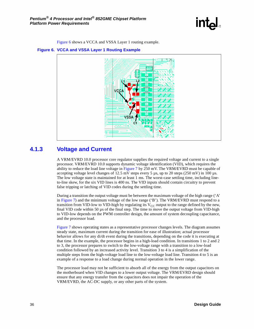
36 Design Guide
Pentium® 4 Processor and Intel® 852GME Chipset PlatformPlatform Power Requirements
Figure 6 shows a VCCA and VSSA Layer 1 routing example.
4.1.3 Voltage and Current
A VRM/EVRD 10.0 processor core regulator supplies the required voltage and current to a single processor. VRM/EVRD 10.0 supports dynamic voltage identification (VID), which requires the ability to reduce the load line voltage in Figure 7 by 250 mV. The VRM/EVRD must be capable of accepting voltage level changes of 12.5 mV steps every 5 µs, up to 20 steps (250 mV) in 100 µs. The low voltage state is maintained for at least 1 ms. The worst-case settling time, including line-to-line skew, for the six VID lines is 400 ns. The VID inputs should contain circuitry to prevent false tripping or latching of VID codes during the settling time.
During a transition the output voltage must be between the maximum voltage of the high range (‘A’ in Figure 7) and the minimum voltage of the low range (‘B’). The VRM/EVRD must respond to a transition from VID-low to VID-high by regulating its VCC output to the range defined by the new, final VID code within 50 µs of the final step. The time to move the output voltage from VID-high to VID-low depends on the PWM controller design, the amount of system decoupling capacitance, and the processor load.
Figure 7 shows operating states as a representative processor changes levels. The diagram assumes steady state, maximum current during the transition for ease of illustration; actual processor behavior allows for any di/dt event during the transitions, depending on the code it is executing at that time. In the example, the processor begins in a high-load condition. In transitions 1 to 2 and 2 to 3, the processor prepares to switch to the low-voltage range with a transition to a low-load condition followed by an increased activity level. Transition 3 to 4 is a simplification of the multiple steps from the high-voltage load line to the low-voltage load line. Transition 4 to 5 is an example of a response to a load change during normal operation in the lower range.
The processor load may not be sufficient to absorb all of the energy from the output capacitors on the motherboard when VID changes to a lower output voltage. The VRM/EVRD design should ensure that any energy transfer from the capacitors does not impair the operation of the VRM/EVRD, the AC-DC supply, or any other parts of the system.
Figure 6. VCCA and VSSA Layer 1 Routing Example

Design Guide 37
Pentium® 4 Processor and Intel® 852GME Chipset PlatformPlatform Power Requirements
4.1.4 Voltage Identification for VRM/EVRD 10.0
There are five VID balls/pins on the processor. These signals may be used to support automatic selection of VCC voltages. They are needed to cleanly support voltage specification variations for current and future processors. VIDs are defined in Table 4. The VID[4:0] signals are open drain on the processor and need pull-up resistors to 3.3 V on the motherboard.
The VRM/EVRD accepts six lines to set the nominal voltage. When the VID[4:0] inputs are all high (in this case, VID5 is not important), such as when no processor is installed, the VRM/EVRD should disable its output. When this disable code appears during previously normal operation, the VRM/EVRD should turn off its output within 500 ms. Other platform components may use VID inputs and may require tighter limits than specified in Table 4.
VID[4:0] are compatible with the Pentium® 4 using five-bit VID codes. VID [5] has to be set as high when five-bit VID codes are used. VID [5:0] will be used on processors with six-bit VID codes.
Table 3 presents the VID specifications.
Figure 7. Processor Transition States
VID High Load Line
1
2
3
4
Icc-max
5 VID Low Load Line
A
B
Table 3. VID Specifications
Symbol Parameter Min Max Units Notes
VIH Input High Voltage 0.8 3.465 V †
VIL Input Low Voltage 0 0.4 V †
† Other platform components may use VID inputs and may require tighter limits.

38 Design Guide
Pentium® 4 Processor and Intel® 852GME Chipset PlatformPlatform Power Requirements
Table 4 presents VID information.
Table 4. Voltage Identification (VID)
Processor Pins (0 = low, 1 = high) Vout(V) Processor Pins (0 = low, 1 = high) Vout
(V)
VID4 VID3 VID2 VID1 VID0 VID5 VID4 VID3 VID2 VID1 VID0 VID5
0 1 0 1 0 0 0.8375 1 1 0 1 0 0 1.2125
0 1 0 0 1 1 0.8500 1 1 0 0 1 1 1.2250
0 1 0 0 1 0 0.8625 1 1 0 0 1 0 1.2375
0 1 0 0 0 1 0.8750 1 1 0 0 0 1 1.2500
0 1 0 0 0 0 0.8875 1 1 0 0 0 0 1.2625
0 0 1 1 1 1 0.9000 1 0 1 1 1 1 1.2750
0 0 1 1 1 0 0.9125 1 0 1 1 1 0 1.2875
0 0 1 1 0 1 0.9250 1 0 1 1 0 1 1.3000
0 0 1 1 0 0 0.9375 1 0 1 1 0 0 1.3125
0 0 1 0 1 1 0.9500 1 0 1 0 1 1 1.3250
0 0 1 0 1 0 0.9625 1 0 1 0 1 0 1.3375
0 0 1 0 0 1 0.9750 1 0 1 0 0 1 1.3500
0 0 1 0 0 0 0.9875 1 0 1 0 0 0 1.3625
0 0 0 1 1 1 1.0000 1 0 0 1 1 1 1.3750
0 0 0 1 1 0 1.0125 1 0 0 1 1 0 1.3875
0 0 0 1 0 1 1.0250 1 0 0 1 0 1 1.4000
0 0 0 1 0 0 1.0375 1 0 0 1 0 0 1.4125
0 0 0 0 1 1 1.0500 1 0 0 0 1 1 1.4250
0 0 0 0 1 0 1.0625 1 0 0 0 1 0 1.4375
0 0 0 0 0 1 1.0750 1 0 0 0 0 1 1.4500
0 0 0 0 0 0 1.0875 1 0 0 0 0 0 1.4625
1 1 1 1 1 1 OFF† 0 1 1 1 1 1 1.4750
1 1 1 1 1 0 OFF† 0 1 1 1 1 0 1.4875
1 1 1 1 0 1 1.1000 0 1 1 1 0 1 1.5000
1 1 1 1 0 0 1.1125 0 1 1 1 0 0 1.5125
1 1 1 0 1 1 1.1250 0 1 1 0 1 1 1.5250
1 1 1 0 1 0 1.1375 0 1 1 0 1 0 1.5375
1 1 1 0 0 1 1.1500 0 1 1 0 0 1 1.5500
1 1 1 0 0 0 1.1625 0 1 1 0 0 0 1.5625
1 1 0 1 1 1 1.1750 0 1 0 1 1 1 1.5750
1 1 0 1 1 0 1.1875 0 1 0 1 1 0 1.5875
1 1 0 1 0 1 1.2000 0 1 0 1 0 1 1.6000
† Output disabled - the same as de-asserting the output enable input.

Design Guide 39
Pentium® 4 Processor and Intel® 852GME Chipset PlatformPlatform Power Requirements
4.1.5 VCC_CORE Power Sequencing
The VRM/EVRD must support platforms with defined power-up sequences. Figure 3 shows a block diagram of a power sequencing implementation, and Figure 8 shows a timing diagram of the power sequencing requirements.
4.1.6 Voltage Regulator Design Recommendations
Intel recommends using a VRD 10.0 voltage regulator DC-to-DC converter for processor Vcc core voltage rail. These regulators should be capable of accepting a 5-bit VID code to indicate the voltage required by the individual processor unit. For more information, refer to Voltage Regulator-Down (VRD) 10.0 Design Guidelines for the actual specifications. The following section describes some guidelines for the design of the voltage regulator in terms of design topology and component selection. This is done to ensure design and component compatibility.
Figure 8. Power-On Sequence Timing Diagram
NOTES:1. Vtt comes up at the application of system power to the Vtt VR. Vtt is used to supply VID power to the
processor.2. Vtt VR generates VIDPWRGD, to latch the processor’s VID outputs and enable the Vcc VR, after the Vtt
supply is valid.3. Vcc_PWRGD is generated by the Vcc VR and may be used elsewhere in the system.4. VIDPWRGD must de-activate and Vcc must be disabled immediately when Vtt becomes invalid.5. Verify that Vcc is enabled as soon as possible after VIDPWRGD is valid.6. Verify that Vcc_PWRGD asserts between 0 and 10 ms after Vcc reaches 90% of the final value.
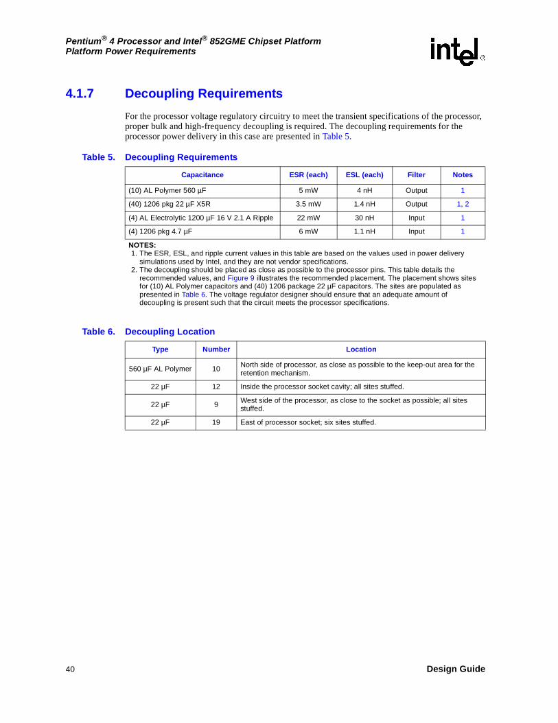
40 Design Guide
Pentium® 4 Processor and Intel® 852GME Chipset PlatformPlatform Power Requirements
4.1.7 Decoupling Requirements
For the processor voltage regulatory circuitry to meet the transient specifications of the processor, proper bulk and high-frequency decoupling is required. The decoupling requirements for the processor power delivery in this case are presented in Table 5.
Table 5. Decoupling Requirements
Capacitance ESR (each) ESL (each) Filter Notes
(10) AL Polymer 560 µF 5 mW 4 nH Output 1
(40) 1206 pkg 22 µF X5R 3.5 mW 1.4 nH Output 1, 2
(4) AL Electrolytic 1200 µF 16 V 2.1 A Ripple 22 mW 30 nH Input 1
(4) 1206 pkg 4.7 µF 6 mW 1.1 nH Input 1
NOTES:1. The ESR, ESL, and ripple current values in this table are based on the values used in power delivery
simulations used by Intel, and they are not vendor specifications.2. The decoupling should be placed as close as possible to the processor pins. This table details the
recommended values, and Figure 9 illustrates the recommended placement. The placement shows sites for (10) AL Polymer capacitors and (40) 1206 package 22 µF capacitors. The sites are populated as presented in Table 6. The voltage regulator designer should ensure that an adequate amount of decoupling is present such that the circuit meets the processor specifications.
Table 6. Decoupling Location
Type Number Location
560 µF AL Polymer 10 North side of processor, as close as possible to the keep-out area for the retention mechanism.
22 µF 12 Inside the processor socket cavity; all sites stuffed.
22 µF 9 West side of the processor, as close to the socket as possible; all sites stuffed.
22 µF 19 East of processor socket; six sites stuffed.

Design Guide 41
Pentium® 4 Processor and Intel® 852GME Chipset PlatformPlatform Power Requirements
Figure 9. Decoupling Placement

42 Design Guide
Pentium® 4 Processor and Intel® 852GME Chipset PlatformPlatform Power Requirements
4.1.8 Layout
In an eight-layer board, two layers should be used for VCC_CPU, and two layers should be used for ground. Traces are not sufficient for supplying power to the processor due to the high current and low resistance required to meet the processor voltage specifications. To satisfy these requirements, shapes that encompass the power delivery part of the processor pin field are required. Figure 10 through Figure 12 show examples of how to use shapes to deliver power to the processor.
The processor socket has 478 pins with 50 mil pitch. The routing of the signals, power and ground pins require creation of many vias. These vias cut up the power and ground planes beneath the processor resulting in increased inductance of these planes. To provide the best path through the via field, Intel recommends that vias be shared for two processor ground pins and for two processor power pins. Figure 13 shows this via sharing.
Figure 10. Top Layer Power Delivery Shape (VCCP)

Design Guide 43
Pentium® 4 Processor and Intel® 852GME Chipset PlatformPlatform Power Requirements
Figure 11. Layer 2 and Layer 7 Power Delivery Shape (VSS)

44 Design Guide
Pentium® 4 Processor and Intel® 852GME Chipset PlatformPlatform Power Requirements
Figure 12. Bottom Layer Power Delivery Shape (VCCP)

Design Guide 45
Pentium® 4 Processor and Intel® 852GME Chipset PlatformPlatform Power Requirements
The switching voltage regulators typically used for processor power delivery require the use of the feedback signal for output error correction. Previous 478-pin socket platforms required sensing the voltage regulator feedback from the socket or the system board voltage plane. For this platform using VRD10 controllers, Intel is evaluating whether die sense provides a performance benefit versus socket sense. To provide maximum flexibility for this design, Intel recommends that the system board be routed with an option for both socket feedback and die feedback. This design guide will be updated with the final recommendation for either socket or die sense once the analysis has been completed.
The socket load line defined in the Voltage Regulator-Down (VRD 10.0) Design Guidelines is defined at pins AC14 (VCC_CPU) and AC15 (VSS); validate the socket load line from these pins as well. These pins are located approximately in the center of the pin field on the north side of the processor. Connect socket feedback for the voltage regulator controller close to this area of the power delivery shape using wide, low inductive traces. The die loadline is defined at the processor VCC_SENSE and VSS_SENSE pins. Take the die feedback from these pins using wide, low inductive traces.
Figure 13. Shared Power and Ground Vias

46 Design Guide
Pentium® 4 Processor and Intel® 852GME Chipset PlatformPlatform Power Requirements
Four 0 Ω resistors may be used as shown in Figure 14 to create a manufacturing stuffing option to implement either die or socket sense.
4.1.9 Thermal Considerations
For a power delivery solution to meet the Flexible Motherboard (FMB) requirements, it must be able to deliver a fairly high amount of current. This high amount of current also requires that the solution is able to dissipate the associated heat generated by the components and keep all of the components and the PCB within their thermal specifications. It is the responsibility of OEMs to evaluate their component configurations, system airflow, and layout to ensure adequate thermal performance of the processor power delivery solution.
Intel recommends that the system boards be designed to support the full Pentium 4 processor FMB guidelines. These guidelines include an ICC_MAX electrically for brief time periods. Design the voltage regulator solution to support a minimum of VR_TDC indefinitely within the envelope of operation conditions of the system. The VR_TDC limits of the system board are typically governed by the system board thermal limits. Intel recommends that system boards designed to the above guidelines implement a VR thermal monitor circuit.
The voltage regulator shown is a two-phase solution with four FETs per phase. The layout is optimized to provide adequate thermal relief for the motherboard and other components. The voltage regulator thermal performance was validated using the Intel reference heatsink and the boxed processor heatsink in a representative chassis running in a 25° C and 35° C external ambient environment.
The specifications for ICC_MAX of the Pentium 4 processor are contained in the processor datasheet.
Figure 14. Routing of VR Feedback Signals
B2617-01
ProcessorVCC
Plane
VCCSENSE/VSSSENSE pins
Resistor stuffingoption - only onepair populated
VRD10

Design Guide 47
Pentium® 4 Processor and Intel® 852GME Chipset PlatformPlatform Power Requirements
4.1.10 Simulation
To completely model the system board, include the inductance and resistance that exists in the cables, connectors, PCB planes, pins and body of components (such as resistors and capacitors), processor socket, and the voltage regulator module. More detailed models showing these effects are shown in Figure 15.
Table 7 lists model parameters for the system board shown in Figure 15.
Figure 15. Detailed Power Distribution Model for Processor with Voltage Regulatoron System Board
B1602-01
L9L8L6L5L3L21.1
Probe pointfor VCCP
at Skt.
Bul
ks n
orth
of
Skt
MLC
Cs
nort
h of
Skt
MLC
Cs
in S
kt C
avity
(sou
th)
MLC
Cs
in S
kt C
avity
(nor
th)
ControllerFB Nets
connectedhere
Probe pointfor VCCP
at Skt.
MLC
Cs
sout
h of
Skt
Bul
ks s
outh
of S
kt
NorthSide
PwrDel
SouthSide
PwrDel
R=0.27 mΩL=80 pH
R=0.64 mΩL=200 pH
R=0.329 mΩL=104 pH
R=0.196 mΩL=52 pH
R=0.392 mΩL=104 pH
R=0.33 mΩL=113 pH
R=0.27 mΩL=80 pH
L4 L7
R=0.810 mΩL=78.6 pH
R=0.829 mΩL=80.5 pH
Rload = 1 mΩ
S1
Vstim(Ron and Roff setby step current)
Table 7. Pentium® 4 Processor Power Delivery Model Parameters
Segment Resistance Inductance
L1 0.27 mΩ 80 pH
L2 0.33 mΩ 113 pH
L3 0.392 mΩ 104 pH
L4 0.829 mΩ 80.5 pH
L5 0.196 mΩ 52 pH
L6 0.329 mΩ 104 pH
L7 0.810 mΩ 78.6 pH
L8 0.64 mΩ 200 pH
L9 0.27 mΩ 80 pH

This page intentionally left blank.
48 Design Guide
Pentium® 4 Processor and Intel® 852GME Chipset PlatformPlatform Power Requirements

Design Guide 49
Pentium® 4 Processor and Intel® 852GME Chipset PlatformIntegrated Graphics Display Port
Integrated Graphics Display Port 5
The Intel® 82852GME GMCH contains three display ports: an analog RAMDAC, a dedicated LVDS port, and two 12-bit Digital Video Out (DVO) devices. Section 5.1 discusses the CRT and RAMDAC routing requirements. Section 5.2 discusses the dedicated LVDS port. Section 5.3 discusses the DVO design guideline. Section 5.4 provides recommendations for a flexible modular design guideline for the DVO and DVOC muxed interface. Section 5.6 provides recommendations for the GPIO signal group.
5.1 Analog RGB/CRT Guidelines
5.1.1 RAMDAC/Display Interface
The Intel® 852GME chipset integrated graphics/chipset design interfaces to an analog display through a RAMDAC. The RAMDAC is a subsection of the graphics controller display engine and consists of three identical 8-bit digital-to-analog converter (DAC) channels, one for the display’s red, green, and blue electron guns.
Each RGB output is terminated twice with 75 Ω resistance: One 75 Ω resistance is connected from the DAC output to the board ground, and the other termination resistance exists within the display. The equivalent DC resistance at the output of each DAC is 37.5 Ω. The current output from each DAC flows into this equivalent resistive load to produce a video voltage, without the need for external buffering. There is also an LC pi-filter on each channel that is used to reduce high-frequency noise and to reduce EMI. In order to maximize the performance, match the filter impedance, cable impedance, and load impedance.
Since DAC runs at speeds of up to 350 MHz, pay special attention to signal integrity and EMI. RGB routing, component selection, cable and load impedance (monitor). They all play a large role in an analog display’s quality and robustness. This holds true for all resolutions, but especially for those at 1600 x 1200 resolutions or higher.
5.1.2 Reference Resistor (REFSET)
A reference resistor, REFSET, is used to set the reference current for the DAC. This resistor is an external resistor with a 1% tolerance that is placed on the circuit board. A reference resistor may be selected from a range between 124 Ω and 137 Ω (1%) with a typical value of 128 Ω. Based on board design, DAC RGB outputs may be measured when the display is completely white. When the RGB voltage value is between 665 mV and 770 mV, the video level is within VESA specification and the resistor value that was chosen is optimal for board design.

50 Design Guide
Pentium® 4 Processor and Intel® 852GME Chipset PlatformIntegrated Graphics Display Port
A reference voltage is generated on the Intel 82852GME GMCH from a bandgap voltage reference circuit. The bandgap reference voltage level is approximately 1.2 V and this voltage reference is divided by four to generate the reference voltage. The VESA video standard defines the LSB current for each DAC channel. The RAMDAC reference current is designed on-die to be equal to 32LSB.
Therefore, the external reference resistor value is defined as:
Equation 1. REFSET Equation
Resistor values of 128 Ω and 137 Ω are standard 1% precision resistor values.
5.1.3 RAMDAC Board Design Guidelines
In order for the DAC to successfully run at speeds up to 350 MHz, Intel recommends the following guidelines when routing the analog RAMDAC signals:
• Each analog R, G, B signal be routed single-ended. Route the analog RGB signals with an impedance of 37.5 Ω.
• These routes be on an inner routing layer and that it be shielded with VSS planes, if possible.
• Use 20 mil spacing between DAC channels and to other signals.
The RGB signals require pi filters that should be placed near the VGA connector. It consists of two 3.3 pF caps with a 75 Ω at 100 MHz FB between them. The RGB signals should have a 75 Ω 1% terminating pull-down resistor. Ground the complement signals (R#, G#, and B#) to the ground plane.
Intel recommends that the pi filter and terminating resistors be placed as close as possible to the VGA connector. After the 75 Ω termination resistor, the RGB signals should continue on to their pi filters and the VGA connector, and be routed with a 75 Ω impedance (~ 5 mil traces).
The RGB signals also require protection diodes between 1.5 V and ground. Use diodes with low C ratings (~5 pF max) and small leakage current (~ 10 A at 120° C) and properly decouple them with a 0.1 µF cap. Place these diodes and decoupling to minimize power rail inductance. The choice between diodes (or diode packs) should comprehend the recommended electrical characteristics in addition to cost.
The RGB signals should be length matched as closely as possible (from the Intel 82852GME GMCH to VGA connector) and should not exceed 200 mils of mismatch.
REFSETVreferenceIreference-----------------------------
Vbg 4⁄( )
32 73.2uA( )⋅--------------------------------- 128Ω= = =

Design Guide 51
Pentium® 4 Processor and Intel® 852GME Chipset PlatformIntegrated Graphics Display Port
5.1.4 Intel® 852GME Chipset DAC Routing Guidelines
Figure 16 shows the Intel 852GME chipset DAC routing guidelines.
The Intel 852GME chipset DAC channel (red, green, blue) outputs are routed as single-ended shielded current output routes that are terminated prior to connecting to the video PI-filter and VGA connector.
Figure 16. Intel® 852 GME Chipset DAC Routing Guidelines
B1327-01
1.5 V
1.5 V FB37.5Ω
Place C1 and C2as close to packageas possible
Motherboard
VGAConnector
VCCDACA1 VCCDACA2
IREF VSSDACA
Impedance
75Ω Routes
RED
Pin 1 -Red
Pin 2 -Green
Pin 3 -Blue
RedDACChannel
RED#
C1
C1
D
D
C2
CR1 C
Rset
1.5 V FB37.5Ω
Impedance
75ΩRoutes
BLUE
BlueDACChannel
BLUE#
C1
D
D
CR1 C
1.5 V
FB37.5Ω
Impedance
75ΩRoutes
GREEN
GreenDACChannel
GREEN#
C1
D
D
CR1 C
Place ESD diodes to minimize power rail
inductance - place C1 as close to diodes as possible
Do NOT route any high frequency signals in the
shaded area.
Place components in close proximity to VGA

52 Design Guide
Pentium® 4 Processor and Intel® 852GME Chipset PlatformIntegrated Graphics Display Port
Table 8 presents the recommended Intel 852GME chipset DAC components.
Figure 17 shows the recommended Rset placement.
Table 8. Recommended Intel® 852GME Chipset DAC Components
Recommended DAC Board Components
Component Value Tolerance Power Type
R1 75.0 Ω 1% 1/16 W SMT, Metal Film
Refset 128.0 Ω 1% 1/16 W SMT, Metal Film
C1 0.1 µF 20% ----- SMT, Ceramic
C2 0.01 µF 20% ----- SMT, Ceramic
C 3.3 pF 10% ----- SMT, Ceramic
D PAC DN006 ------- 350 mW
California Micro Devices – ESD diodes for VGA
SOIC package
Or equivalent diode array
FB 75 Ω at100 MHz -------- ------- MuRata* BLM11B750S
Figure 17. Recommended Rset Placement
B1328-01
Intel® 852GMEChipset
RsetResistor
Large via or multiple vias straight down to ground plane
Top Side of Motherboard
128Ω, 1%, 1/16W SMT metal film resistor
Short, wide route connecting the resistor to the IREF ball
Resistor Solder Pads
No toggling signals should be routed near this reference resistor
IREF Ball

Design Guide 53
Pentium® 4 Processor and Intel® 852GME Chipset PlatformIntegrated Graphics Display Port
Figure 18 shows the recommended DAC R, G, B output routing and termination resistor layout.
5.1.5 DAC Power Requirements
The DAC requires a 1.5 V supply through its two VCCADAC balls. The two may share a set of capacitors, 0.1 µF and 0.01 µF, but this connection should have low inductance. Separate analog power or ground planes are not required for the DAC.
However, since the DAC is an analog circuit, it is particularly sensitive to AC noise seen on its power rail. Ensure that designs provide as clean and quiet a supply as possible to the VCCA_DAC. Additional filtering and/or separate voltage rail may be needed to do so.
• Video DAC Power Supply DC Specification: 1.50 V ± 5%
• Video DAC Power Supply AC Specification:
— ± 0.3% from 0.10 Hz to 10 MHz
— ± 0.95% from 10 MHz to max pixel clock frequency
• Absolute minimum voltage at the VCCA package ball = 1.40 V
Refer to the latest Intel® 852GME Chipset GMCH and Intel® 852PM Chipset MCH Datasheet for AC/DC specification.
Figure 18. Recommended DAC R, G, B Output Routing and Termination Resistor Layout
B1329-01
Intel® 852GMEChipset
DACOutput
(e.g., BLUE)
ComplementOutput
(e.g., BLUE)
75.0
VGA-IIFilter
Large via or multiple vias
straight down to ground plane
75.0Ω, 1%, 1/16W SMT metal film resistor
Via to ground plane
No toggling signals should be routed near these video outputs
20 mil Space between channels 20 mil Space between channels
37.5ΩTrace Impedance 75Ω Trace Impedance
Switch

54 Design Guide
Pentium® 4 Processor and Intel® 852GME Chipset PlatformIntegrated Graphics Display Port
5.1.6 HSYNC and VSYNC Design Considerations
HSYNC and VSYNC signals are connected to the analog display attached to the VGA connector. These are 3.3 V outputs from the GMCH. Some monitors have been found to drive HSYNC and VSYNC signals during reset. Because these signals are used as straps on the 852GME, the GMCH can enter into an illegal state under these conditions. In order to prevent these signals from being driven to the GMCH during reset, system designers must ensure GMCH is isolated from any monitor driving HSYNC or VSYNC while PCI_RST# is active. Appropriate logic is required between the GMCH and the VGA connector.
The recommended option is to use a unidirectional buffers (high impedance buffers) on each of these signals. For each of the HSYNCH and VSYNC signals, a footprint for a series resistors must be placed between GMCH and the unidirectional buffer to prevent excessive overshoot and undershoot at the input of the buffer. Consideration should also be taken in designing the filter circuit on the output of these buffers to ensure that the VESA electrical specifications for video signals are met at the VGA connector. Customers are strongly encouraged to perform complete signal integrity validation at the input of the buffer and the VGA connectors.
5.1.7 DDC and I2C Design Considerations
DDCADATA and DDCACLK are 3.3 V I/O buffers connecting the GMCH to the monitor. To avoid potential electrical overstress on these signals, bidirectional level-shifting devices are required. These signals require 2.2 kΩ pull-ups (or pull-ups with the appropriate value derived from simulation) on each of these signals. See Section 5.5 for additional pull up recommendations for the DDC (GPIO) signal group.
5.2 LVDS Transmitter Interface
The Intel LVDS (Low Voltage Differential Signaling) Transmitter serializer converts up to 24 bits of parallel digital RGB data, (eight bits per RGB), along with up to four bits for control (SHFCLK, HSYNC, VSYNC, DE) into two, 4 channel serial bit streams, for output by the LVDS Transmitter.
The transmitter is fully differential and utilizes a current mode drive with a high impedance output. The drive current develops a differential swing in the range of 250 mV to 450 mV across a 100 Ω termination load.
The parallel digital data is serially converted to a 7 bit serial bit stream that is transmitted over the eight channel LVDS interface at 7x the input clock. The differential output clock channel transmits the output clock at the input clock frequency. The differential output channels transmit the data at the 7x clock rate (1 bit time is 7x the input clock) and the 7x serializer synchronizes and regenerates an input clock from 35 MHz to 112 MHz. Typical operation is at 65 MHz (15.4 ns), therefore, at a 7x clock rate, 1 bit time would be 2.2 ns. With data cycle times as small as 2.2 ns, propagation delay mismatch is critical, such that intra-channel skew (skew between the inverting and non-inverting output) must be kept minimal.
LIBG Pin is a current reference on the LVDS interface. A 1.5 kΩ resistor is required unless an 855GME platform is being used with external graphics only option
The following differential signal groups comprise the LVDS Interface. The topology rules for each group are defined in subsequent sections. Table 9 presents the signal group and signal pair names.

Design Guide 55
Pentium® 4 Processor and Intel® 852GME Chipset PlatformIntegrated Graphics Display Port
5.2.1 Length Matching Constraints
The routing guidelines presented in the following subsections define the recommended routing topologies, trace width and spacing geometries, and absolute minimum and maximum routed lengths for each signal group. These recommendations are provided to achieve optimal SI and timing. In addition to the absolute length limits provided, more restrictive length matching requirements are also provided. The additional requirements further restrict the minimum to maximum length range of each signal group with respect to clock strobe, within the overall boundaries defined in the guideline tables, as required to ensure adequate timing margins. These secondary constraints are referred to as length matching constraints. The amount of minimum to maximum length variance allowed for each group around the clock strobe reference length varies from signal group to signal group depending on the amount of timing variation that may be tolerated. Refer to Table 10 for LVDS length matching requirements.
Each LVDS channel is length matched to the LVDS strobe signals. The strobes on a given channel are matched to within ± 25 mils of the target length.
5.2.1.1 LVDS Package Length Compensation
As mentioned in Section 5.2.1, all length matching is done from GMCH die-pad to LVDS connector pin. The reason for this is to compensate for the package length variation across each signal group in order to minimize timing variance. The GMCH does not equalize package lengths internally as some previous GMCH components have, and therefore, the GMCH requires a length matching process. See Table 12 for the Intel 852GME chipset LVDS package lengths information.
Table 9. Signal Group and Signal Pair Names
Channel Signal Group Signal Pair Names
Channel A Clocks ICLKAM, ICLKAP
Data Bus IYAM[3:0], IYAP[3:0]
Channel B Clocks ICLKBM, ICLKBP
Data Bus IYBM[3:0], IYBP[3:0]
Table 10. LVDS Signal Trace Length Matching Requirements
Signal Group Data pair Signal Matching
Clock Strobes Associated With the
ChannelStrobe Matching
ChannelA
IYAM0, IYAP0 ± 20 mils
ICLKAM, ICLKAP ± 20 mils IYAM1, IYAP1 ± 20 mils
IYAM2, IYAP2 ± 20 mils
IYAM3, IYAP3 ± 20 mils
ChannelB
IYBM0, IYBP0 ± 20 mils
ICLKAM, ICLKAP ± 20 mils IYBM1, IYBP1 ± 20 mils
IYBM2, IYBP2 ± 20 mils
IYBM3, IYBP3 ± 20 mils
NOTE: All length matching formulas are based on GMCH die-pad to LVDS connector pin total length. Package length tables are provided for all signals in order to facilitate this pad to pin matching.

56 Design Guide
Pentium® 4 Processor and Intel® 852GME Chipset PlatformIntegrated Graphics Display Port
Do not confuse package length compensation with length matching as discussed in the previous section. Length matching refers to constraints on the minimum and maximum length bounds of a signal group based on clock length, whereas package length compensation refers to the process of adjusting out package length variance across a signal group. There is of course some overlap in that both affect the target length of an individual signal. Intel recommends that the initial route be completed based on the length matching formulas in conjunction with nominal package lengths and that package length compensation be performed as secondary operation.
5.2.2 LVDS Routing Guidelines
Each LVDS channel is required to be length matched to within +/- 20 mils of the LVDS clock strobe signals. The two complementary signals in each clock strobe pair as well as in each data pair are also required to be length matched to within +/- 20 mils of each other. Table 11 presents the LVDS signal group routing guidelines.
Table 11. LVDS Signal Group Routing Guidelines
Parameter Definition
Signal Group LVDS
Topology Differential Pair Point to Point
Reference Plane Ground Referenced
Differential Mode Impedance (Zdiff) 100 Ω ± 15%
Nominal Trace Width 4 mils
Nominal Pair Spacing (edge to edge) 7 mils
Minimum Pair to Pair Spacing (See exceptions for breakout region below.) 20 mils
Minimum Serpentine Spacing 20 mils
Minimum Spacing to Other LVDS Signals (See exceptions for breakout region below.) 20 mils
Minimum Isolation Spacing to non-LVDS Signals 20 mils
Maximum Via Count 2 (per line)
Package Length Range – P1 550 mils ± 150 mils
(See LVDS package length Table 12 for exact lengths.)
Total Length – Max 10 inches
Data to Clock Length Matching Match all segments to within ± 20 mil of associated clock pair
Clock to Clock# Length Matching(Total Length) Match clocks to ± 20 mils.
Data to Data# Length Matching (Total Length) Match data to ± 20 mils
Breakout Exceptions
(Reduced geometries for GMCH breakout region)
The breakout section should be as short as possible. Try to maintain trace width as 4 mils, spacing 7 mils, while the spacing between pairs may be 10-20 mils.

Design Guide 57
Pentium® 4 Processor and Intel® 852GME Chipset PlatformIntegrated Graphics Display Port
The traces associated with the LVDS Transmitter timing domain signals are differential traces terminated across 100 Ω ± 15 Ω and routed as:
• Strip-line only
• Isolate all other signals from the LVDS signals to prevent coupling from other sources onto the LVDS lines.
• Use controlled impedance traces that match the differential impedance of your transmission medium (that is, cable) and termination resistor.
Note: Maintain the transmission medium’s Zdiff to 100 Ω ± 15%.)
• Run the differential pair trace lines as close together as possible as soon as they leave the IC, not greater than 10 mils. This helps eliminate reflections and ensure noise is coupled as common mode. Plus, noise induced on the differential lines is much more likely to appear as common mode, which is rejected by the receiver.
• The LVDS Transmitter timing domain signals have a maximum trace length of 10.0 inches. This maximum applies to all of the LVDS Transmitter signals.
• Traces must be ground referenced and must not switch layers between the GMCH and connector.
When choosing cables, it is important to remember:
• Use controlled impedance media. The differential impedance of cable LVDS uses should be 100 Ω. Cables should not introduce major impedance discontinuities that cause signal reflection.
• Balanced cables (twisted pair) are usually better than unbalanced cables (ribbon cable, multi-conductor) for noise reduction and signal quality.
• Cable length must be less than 16 inches.
Table 12 presents the LVDS package lengths.
Table 12. LVDS Package Lengths
Signal Group
GMCH Signal Name
Package Trace
Length (mils)
Signal Group
GMCH Signal Name
Package Trace
Length (mils)
Channel A
ICLKAP 503.7
Channel B
ICLKAP 502.0
ICLKAM 498.8 ICLKAM 499.1
IYAP0 399.6 IYBP0 359.8
IYAM0 385.4 IYBM0 353.7
IYAP1 487.5 IYBP1 524.7
IYAM1 466.2 IYBM1 516.6
IYAP2 572.6 IYBP2 623.3
IYAM2 566.2 IYBM2 604.2
IYAP3 643.2 IYBP3 441.8
IYAM3 637.8 IYBM3 441.7

58 Design Guide
Pentium® 4 Processor and Intel® 852GME Chipset PlatformIntegrated Graphics Display Port
5.3 Digital Video Out Port
The GMCH DVO port interface supports a wide variety of third party DVO compliant devices (for example, TV encoder, TMDS transmitter or integrated TV encoder and TMDS transmitter). The Intel 852GME chipset has two dedicated Digital Video Out Port’s (DVOB and DVOC). Intel’s DVO port is a 1.5 V only interface that may support transactions up to 165 MHz. Some of the DVO port command signals may require voltage translation circuit depending on the third party device.
5.3.1 DVO Interface Signal Groups
5.3.1.1 DVOB Interface Signals
5.3.1.1.1 Input Signals
• DVOBFLDSTL
5.3.1.1.2 Output Data Signals
• DVOBHSYNC
• DVOBVSYNC
• DVOBBLANK#
• DVOBD[11:0]
5.3.1.1.3 Output Strobe Signals
• DVOBCLK (DVOBCLK[0])
• DVOBCLK# (DVOBCLK[1])
5.3.1.2 DVOC Interface Signals
5.3.1.2.1 Input Signals
• DVOCFLDSTL
5.3.1.2.2 Output Data Signals
• DVOCHSYNC
• DVOCVSYNC
• DVOCBLANK#
• DVOCD[11:0]
5.3.1.2.3 Output Strobe Signals
• DVOCCLK (DVOCCLK[0])
• DVOCCLK# (DVOCCLK[1])

Design Guide 59
Pentium® 4 Processor and Intel® 852GME Chipset PlatformIntegrated Graphics Display Port
5.3.1.3 Common Signals for Both DVO Ports
5.3.1.3.1 Input Signals
• DVOBCCLKINT
• DVOBCINTR#
• ADDID[7:0]
• DVODETECT
5.3.1.3.2 Voltage References, PLL Power Signals
• DVORCOMP
• GVREF
5.3.2 DVOB and DVOC Port Interface Routing Guidelines
For Intel 852GME chipset platforms, guidelines apply for both interfaces.
5.3.2.1 Length Mismatch Requirements
The routing guidelines presented in the following subsections define the recommended routing topologies, trace width and spacing geometries, and absolute minimum and maximum routed lengths for each signal group, which are recommended to achieve optimal SI and timing. In addition to the absolute length limits provided in the individual guideline tables, more restrictive length matching requirements are also provided that further restrict the minimum to maximum length range of each signal group with respect to clock strobe, within the overall boundaries defined in the guideline tables, as required to ensure adequate timing margins. These secondary constraints are referred to as length matching constraints. The amount of minimum to maximum length variance allowed for each group around the clock strobe reference length varies from signal group to signal group depending on the amount of timing variation, which may be tolerated. Refer to Table 13 for DVO length matching requirements.
Table 13. DVO Interface Trace Length Mismatch Requirements
Data Group Signal Matching to Strobe Clock
DVO Clock Strobes Associated With the
GroupClock Strobe Matching Notes
DVOBD [11:0] ± 100 mils DVOBCLK[1:0] ± 10 mils 1, 2
DVOCD [11:0] ± 100 mils DVOCCLK[1:0] ± 10 mils 1, 2
NOTES:1. Data signals of the same group should be trace length matched to the clock within ± 100 mil including
package lengths.2. All length matching formulas are based on GMCH die-pad to DVO device pin total length. Package
length table are provided for all signals in order to facilitate this pad to pin matching.
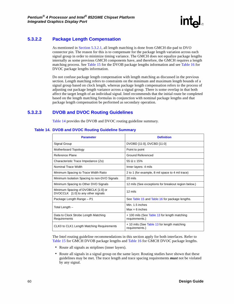
60 Design Guide
Pentium® 4 Processor and Intel® 852GME Chipset PlatformIntegrated Graphics Display Port
5.3.2.2 Package Length Compensation
As mentioned in Section 5.3.2.1, all length matching is done from GMCH die-pad to DVO connector pin. The reason for this is to compensate for the package length variation across each signal group in order to minimize timing variance. The GMCH does not equalize package lengths internally as some previous GMCH components have, and therefore, the GMCH requires a length matching process. See Table 15 for the DVOB package lengths information and see Table 16 for DVOC package lengths information.
Do not confuse package length compensation with length matching as discussed in the previous section. Length matching refers to constraints on the minimum and maximum length bounds of a signal group based on clock length, whereas package length compensation refers to the process of adjusting out package length variance across a signal group. There is some overlap in that both affect the target length of an individual signal. Intel recommends that the initial route be completed based on the length matching formulas in conjunction with nominal package lengths and that package length compensation be performed as secondary operation.
5.3.2.3 DVOB and DVOC Routing Guidelines
Table 14 provides the DVOB and DVOC routing guideline summary.
The Intel routing guideline recommendations in this section apply for both interfaces. Refer to Table 15 for GMCH DVOB package lengths and Table 16 for GMCH DVOC package lengths.
• Route all signals as striplines (inner layers).
• Route all signals in a signal group on the same layer. Routing studies have shown that these guidelines may be met. The trace length and trace spacing requirements must not be violated by any signal.
Table 14. DVOB and DVOC Routing Guideline Summary
Parameter Definition
Signal Group DVOBD [11:0], DVCBD [11:0]
Motherboard Topology Point to point
Reference Plane Ground Referenced
Characteristic Trace Impedance (Zo) 55 Ω ± 15%
Nominal Trace Width Inner layers: 4 mils
Minimum Spacing to Trace Width Ratio 2 to 1 (for example, 8 mil space to 4 mil trace)
Minimum Isolation Spacing to non-DVO Signals 20 mils
Minimum Spacing to Other DVO Signals 12 mils (See exceptions for breakout region below.)
Minimum Spacing of DVOBCLK [1:0] or DVOCCLK [1:0] to any other signals 12 mils
Package Length Range – P1 See Table 15 and Table 16 for package lengths.
Total Length – Min. 1.5 inches
Max = 6 inches
Data to Clock Strobe Length Matching Requirements
+ 100 mils (See Table 13 for length matching requirements.)
CLK0 to CLK1 Length Matching Requirements + 10 mils (See Table 13 for length matching requirements.)

Design Guide 61
Pentium® 4 Processor and Intel® 852GME Chipset PlatformIntegrated Graphics Display Port
• Route the DVOBCLK[1:0] or DVOCCLK[1:0] signal pairs 4 mils wide and 8 mils apart with a max trace length of six inches. Ensure that this signal pair is a minimum of 12 mils from any adjacent signals.
• In order to break out of the Intel® 82852GME GMCH, the DVOB and/or DVOC data signals may be routed with a trace width of 4 mils and a trace spacing of 7 mils. Separate the signals to a trace width of 4 mils and a trace spacing of 8 mils within 0.3 inch of the GMCH component.
Table 15 presents the DVOB interface package lengths.
Table 15. DVOB Interface Package Lengths
Signal Pin Number Package Length (mils)
DVOBBLANK# L2 583
DVOBCCLKINT M3 520
DVOBCINTR# G2 712
DVOBCLK P3 475
DVOBCLK# P4 439
DVOBD[0] R3 489
DVOBD[1] R5 439
DVOBD[2] R6 343
DVOBD[3] R4 415
DVOBD[4] P6 409
DVOBD[5] P5 387
DVOBD[6] N5 466
DVOBD[7] P2 553
DVOBD[8] N2 568
DVOBD[9] N3 504
DVOBD[10] M1 611
DVOBD[11] M5 510
DVOBFLDSTL M2 566
DVOBHSYNC T6 339
DVOBVSYNC T5 362

62 Design Guide
Pentium® 4 Processor and Intel® 852GME Chipset PlatformIntegrated Graphics Display Port
Table 16 presents the DVOC interface package lengths.
5.3.2.4 DVOB and DVOC Port Termination
The DVO interface does not require external termination.
5.3.3 DVOB and DVOC Assumptions, Definitions, and Specifications
The source synchronous solution space consists of all designs in which the flight time mismatch between a strobe and its associated data is less than the total allowable skew:
Where Tflightdata and Tflightstrobe are the driver-pad-to-receiver-pin flight times of the data and the strobe respectively.
The DVO physical interface is a point-to-point topology using 1.5 V signaling. The DVO uses a 165 MHz clock.
The flight time skew simulations simulate all parameters that could cause a skew between two signals, including motherboard and add-in card line lengths, effective capacitance in the buffer models, crosstalk on each of the different interconnect combinations, data pattern dependencies, and ISI induced skews.
Table 16. DVOC Interface Package Lengths
Signal Pin Number Package Length (mils)
DVOCBLANK# L3 541
DVOCCLK J3 601
DVOCCLK# J2 675
DVOCD[0] K5 489
DVOCD[1] K1 692
DVOCD[2] K3 622
DVOCD[3] K2 685
DVOCD[4] J6 536
DVOCD[5] J5 518
DVOCD[6] H2 720
DVOCD[7] H1 771
DVOCD[8] H3 649
DVOCD[9] H4 625
DVOCD[10] H6 521
DVOCD[11] G3 762
DVOCFLDSTL H5 566
DVOCHSYNC K6 491
DVOCVSYNC L5 440
Tskew Tfl ightdata Tflightstrobe–=

Design Guide 63
Pentium® 4 Processor and Intel® 852GME Chipset PlatformIntegrated Graphics Display Port
5.3.4 DVOB and DVOC Simulation Method
A model for simulation purposes is shown in Figure 19. The DVO component is a third party-chip.
Figure 20 shows the driver-receiver waveforms relationship specification.
The setup margin and the hold margin for a particular design depends on the values of the data valid times and the data setup and hold times on both the driver and the receiver sides. However, available margins are not absolute values. Any skew due to routing and loading differences, any coupling differences in the parallel traces, and any effects of SSO (ISI, ground bounce, etc.) must be accounted for in the timing budget as they reduce the total available margin for the design.
Figure 19. DVOB and DVOC Simulations Model
B1332-01
DVO(Device)
Intel® 82852GMEGMCH
tDVb, tDVa
tDSu, tDh
DVO Inferface DVOB / DVOC Control, Data
Figure 20. Driver-Receiver Waveforms Relationship Specification
B1333-01
DriverStrobe
DriverData Data1 Data2 Data3 Data4
tDVbtDVa
tDSutDh
ReceiverStrobe
Data Delay Clock Delay
ReceiverData Data1 Data2 Data3 Data4

64 Design Guide
Pentium® 4 Processor and Intel® 852GME Chipset PlatformIntegrated Graphics Display Port
Table 17 presents the allowable interconnect skew calculation.
All numbers in this table are from the Intel 82852GME GMCH specification documents that are applicable for this interface. For third-party receiver devices, refer to appropriate third-party vendor specifications.
5.4 DVOB and DVOC Port Flexible (Modular) Design
The GMCH supports flexible design interfaces described in this section.
5.4.1 DVOB and DVOC Module Design
The Intel 82852GME GMCH supports a DVO module design connected to the GMCH through a generic connector. Simulation method is the same as in Section 5.3.4. Lengths L1 and L2 are determined by simulation as L1= 4 inches and L2= 2 inches. Refer to Figure 21 for the DVO enabled simulation model and Figure 22 for the generic connector parasitic model.
Table 17. Allowable Interconnect Skew Calculation
Component Skew Element Symbol Setup Hold Units
Driver Data Valid before Strobe tDVb 570 ps
Data Valid after Strobe tDVa 770 ps
Interconnect Allowable Skew Vendor Specific
Vendor Specific ps
Receiver Data Setup to Strobe tDSu Vendor Specific ps
Data Hold from Strobe tDh Vendor Specific ps
Figure 21. DVO Enabled Simulation Model
B1334-01
Connectorwith DVOModule
Intel® 82852GMEGMCH
tDVb, tDVa,tDSu, tDh
tDVb, tDVa,tDSu, tDh
DVOB &DVOC
Inferface
GenericConnector
L1 L2

Design Guide 65
Pentium® 4 Processor and Intel® 852GME Chipset PlatformIntegrated Graphics Display Port
Route all signals as striplines (inner layers). Route all signals in a signal group on the same layer. Routing studies have shown that these guidelines may be met. The trace length and trace spacing requirements must not be violated by any signal. Keep the trace length mismatch for all signals within a signal group as close to ± 100 mils with respect to the strobe clocks as possible to provide optimal timing margin. Each strobe pair must be separated from other signals by at least 12 mils.
Table 18 presents the DVO enabled routing guideline summary.
For DVO module case, the simulation model is the same as Figure 21 and the routing guideline is the same as in Table 18; each strobe pair must be separated from other signals by at least 12 mils. For multiplexed design, more conservative length mismatch (± 0.1 inch) is adopted.
5.4.1.1 Generic Connector Model
Figure 22 shows the generic connector model used in simulation for flexible DVO implementation. This is only for reference; the actual connector may have different parasitic values. Designs using this approach need to be simulated first.
5.5 DVO GMBUS and DDC Interface Considerations
The GMCH DVOB and/or DVOC port controls the video front-end devices through the GMBUS (I2C) interface. The DDCADATA and DDCACLK should be connected to the CRT connector. The GMBUS should be connected to the DVO device, as required by the specifications for those devices. The protocol and bus may be used to configure registers in the TV encoder, TMDS transmitter, or any other external DVI device. The GMCH also has an option to utilize the DDCPCLK and DDCPDATA to collect Extended Display Identification (EDID) from a digital display panel.
Pull-ups (or pull-ups with the appropriate value derived from simulating the signal) typically ranging from 2.2 kΩ to 10 kΩ are required on each of these signals.
Table 18. DVO Enabled Routing Guideline Summary
Signal Maximum Length Trace Width Trace Spacing Length
Mismatch Notes
DVO Timing Domain
L1=4 in
L2=2 in4 mils 8 mils ± 100 mils
Figure 22. Generic Module Connector Parasitic Model
B1335-01
ModuleMotherboard
2.21 pFC2C1
LR
Note: Actual connector may have different parasitic values.
2.5 nH20 mΩ

66 Design Guide
Pentium® 4 Processor and Intel® 852GME Chipset PlatformIntegrated Graphics Display Port
Table 19 presents the possible GMBUS pairs matching options.
When any of the GMBUS pairs (except DDCADATA/DDCACLK for CRT) are not used, 2.2 k –100 kΩ pull-up (or pull-ups with the appropriate value derived from simulating the signal), resistors are required except for LCLKCTRLA/LCLKCTRLB GMBUS pair. This prevents the GMCH DVOB interface from confusing noise on these lines for false cycles.
5.5.1 Leaving the GMCH DVOB or DVOC Port Unconnected
When the motherboard does not implement any of the possible video devices with the DVO port, follow the guidelines recommended on the motherboard. DVO Output signals may be left unconnected if they are not used.
Pull-down resistors are required for the following signals if not used:
• DVOBFLDSTL
• DVOCFLDSTL
• DVOBCCLKINT
Pull-up resistors are required for the following signals if not used:
• DVOBCINTR#
Table 19. GMBUS Pair Mapping and Options
Pair # Signal Name Buffer Type Description Notes
0DDCADATA
3.3 V DDC for Analog monitor (CRT) connection.
This cannot be shared with other DDC or I2C pairs due to legacy monitor issues.DDCACLK
1LCLKCTRLA
3.3 V For control of SSC clock generator devices down on motherboard.
When SSC is not supported, these may be used for DVOB or DVOC GMBUS.LCLKCTRLB
2DDCPDATA
3.3 VDDC for Digital Display connection through the integrated LVDS display port for support for EDID panel.
When EDID panels are not supported. May optionally use as GMBUS for DVOB or DVOC.DDCPCLK
3MDVIDATA
1.5 V GMBUS control of DVI devices (TMDS or TV encoder)
May optionally use as GMBUS for DVOB or DVOC.MDVICLK
4MI2CDATA
1.5 V GMBUS control of DVI devices (TMDS or TV encoder)
May optionally use as GMBUS for DVOB or DVOC.MI2CCLK
5MDDCDATA
1.5 V DDC for Digital Display connection through a TMDS device
May optionally use as GMBUS for DVOB or DVOC.MDDCCLK
NOTE: All GMBUS pairs may be optionally programmed to support any interface and is programmed through the BMP utility.

Design Guide 67
Pentium® 4 Processor and Intel® 852GME Chipset PlatformIntegrated Graphics Display Port
5.6 Miscellaneous Input Signals and Voltage Reference
ADDID[7]: Pull-down to ground with a 1 KΩ resistor when using the DVOB or DVOC port. This is a vBIOS strapping option to load the TPV AIM module for DVOB and DVOC port. Pull-down not required if DVOB or DVOC is not enabled.
ADDID[6:0]: Leave unconnected (NC).
DVODETECT: Leave unconnected (NC) when using the DVOB or DVOC port.
AGPBUSY#: 8.2 KΩ pull up to VCC3.
DVORCOMP: Used to calibrate the DVOB buffers. Connect this signal to ground through a 40.2 Ω 1% resistor using a routing guideline of 10mil trace and 20mil spacing.
DPMS: Connect to 1.5 V version of the ICH4 SUSCLK or a clock that runs during S1.
GVREF: Reference voltage for the DVOB and DVOC input buffers. Refer to Figure 23 for proper signal conditioning.
Figure 23. GVREF Reference Voltage
0.1 µF 0.1 µF
1 KΩ ±1%GVREF (to GMCH)
GVREF (to DVO device)
+ V 1.5 S
1 KΩ ±1%

This page intentionally left blank.
68 Design Guide
Pentium® 4 Processor and Intel® 852GME Chipset PlatformIntegrated Graphics Display Port

Design Guide 69
Pentium® 4 Processor and Intel® 852GME Chipset PlatformSystem Memory Design Guidelines
System Memory Design Guidelines 6
6.1 Introduction
The Intel® 852GME chipset Double Data Rate (DDR) SDRAM system memory interface consists of SSTL-2 compatible signals. These SSTL-2 compatible signals have been divided into several signal groups: Data, Control, Command, CPC, Clock, and Feedback signals. Table 20 summarizes the different signal groupings. Refer to the Intel® 852GME Chipset GMCH and Intel® 852PM Chipset GMCH Datasheet for details on the signals listed.
Table 20. Intel® 852GME Chipset DDR Signal Groups
Group Signal Name Description
Clocks SCK[5:0] DDR-SDRAM differential clocks - (3 per DIMM)
SCK[5:0]# DDR-SDRAM inverted differential clocks - (3 per DIMM)
Data SDQ[63:0] Data Bus
SDQS[7:0] Data Strobes
SDQ[71:64] Check bits for ECC Function
SDM[7:0] Data Mask
Control SCKE[3:0] Clock Enable - (One per device row)
SCS[3:0]# Chip Select - (One per device row)
Command SMA[12:6,3,0] Memory Address Bus
SBA [1:0] Bank Select
SRAS# Row Address Select
SCAS# Column Address Select
SWE# Write Enable
CPC SMA[5,4,2,1] Command per Clock (DIMM0)
SMAB[5,4,2,1] Command per Clock (DIMM1)
Feedback RCVENOUT# Receive Enable Output (no external connection)
RCVENIN# Receive Enable Input (no external connection)

70 Design Guide
Pentium® 4 Processor and Intel® 852GME Chipset PlatformSystem Memory Design Guidelines
6.2 Length Matching and Length Formulas
The routing guidelines presented in the following subsections define Intel’s recommended routing topologies, trace width, and spacing geometries, and absolute minimum and maximum routing lengths for each signal group to achieve optimal SI and timing. In addition to the absolute length limits provided in the individual guideline tables, more restrictive length-matching formulas are also provided that further restrict the minimum to maximum length range of each signal group with respect to clock, within the overall boundaries defined in the guideline tables, as required to ensure adequate timing margins. These secondary constraints are referred to as length-matching constraints, and the formulas used are referred to as length-matching formulas.
All signal groups, except feedback signals, are length matched to the DDR clocks. The clocks on a given DIMM are matched to within ± 25 mils of the target length. A different clock target length may be used for each DIMM. Verify that the difference in clock target lengths between DIMM0 and DIMM1 does not exceed 1 inch. A simple summary of the length matching formulas for each signal group is provided in Table 21.
Package length tables are provided for all signals in order to facilitate this pad-to-pin matching. Apply length formulas to each DIMM slot separately. The full geometry and routing guidelines along with the exact length matching formulas and associated diagrams are provided in the individual signal group guidelines sections below.
6.3 Package Length Compensation
All length matching is done GMCH die-pad to DIMM pin. The reason for this is to compensate for the package length variation across each signal group in order. The Intel® 82852GME GMCH does not equalize package lengths internally as some previous GMCH components have, and therefore, the Intel 82852GME GMCH requires length matching or tuning process. This requirement is based on the belief that length variance in the package based on ball position will be tuned out when the pin escape is completed to the edge of the package. Length matching in the package would create a mismatch at the package edge.
Do not confuse package length compensation with length matching as discussed in the previous section. Length matching refers to constraints on the min and max length bounds of a signal group based on clock length, whereas package length compensation refers to the process of adjusting out package length variation across a signal group. There is some overlap in that both affect the target
Table 21. Length Matching Formats
Signal Group Minimum Length Maximum Length
Control to Clock Clock – 1.5 inches Clock - 0.5 inch
Command to Clock Clock – 1.5 inches Clock + 1.0 inch
CPC to Clock Clock – 1.5 inches Clock - 0.5 inch
Strobe to Clock Clock – 1.5 inches Clock - 0.5 inch
Data to Strobe Strobe – 25 mils Strobe + 25 mils
NOTE: All length-matching formulas are based on GMCH die-pad to DIMM pin total length.

Design Guide 71
Pentium® 4 Processor and Intel® 852GME Chipset PlatformSystem Memory Design Guidelines
length of an individual signal. Intel recommends that the initial route be completed based on the length matching formulas in conjunction with nominal package lengths and that package length compensation be performed as secondary operation where required.
6.4 Topologies and Routing Guidelines
The Intel 852GME chipset’s DDR SDRAM system memory interface implements the low-swing, high-speed, terminated SSTL_2 topology. This section contains information related to the recommended interconnect topologies and routing guidelines for each of the signal groups that comprise the DDR interface. When implemented as defined, these guidelines provide for a robust DDR solution on an Intel 852GME chipset based design. The clock signal group is presented first, since most of the signal groups have length formulas that are based on clock length.
6.4.1 Clock Signals – SCK[5:0], SCK[5:0]#
The clock signal group includes the differential clock pairs SCK[5:0]/SCK[5:0]#. The GMCH generates and drives these differential clock signals required by the DDR interface; therefore, no external clock driver is required for the DDR interface. The GMCH only supports unbuffered DDR DIMMs; three differential clock pairs are routed to each DIMM connector.
Table 22 summarizes the clock signal mapping.
Table 22. Clock Signal Mapping
Signal Relative To
SCK[2:0]/SCK[2:0]# DIMM0
SCK[5:3]/SCK[5:3]# DIMM1

72 Design Guide
Pentium® 4 Processor and Intel® 852GME Chipset PlatformSystem Memory Design Guidelines
6.4.2 Clock Topology Diagram
The Intel 82852GME GMCH provides six differential clock output pairs, or three clock pairs per DIMM socket. The motherboard clock routing topology is shown below for reference. Refer to the routing guidelines in Section 6.4.3 on the following page for detailed length and spacing rules for each segment. Route the clock signals as closely coupled differential pairs over the entire length. Do not allow spacing to other DDR signals to be less than 20 mils. Verify that isolation spacing to non-DDR signals is 25 mils.
Figure 24 shows the DDR clock routing topology (SCK[5:0]/SCK[5:0]#).
6.4.3 DDR Clock Routing Guidelines
Table 23 presents the clock signal group routing guidelines.
Figure 24. DDR Clock Routing Topology (SCK[5:0]/SCK[5:0]#)
B1314-02
GMCHDie Pad
DIMMPads
R1
Intel® 82852GME GMCH
Differential Pairs
L1
L1
P1
P1
L2
L2
Table 23. Clock Signal Group Routing Guidelines (Sheet 1 of 2)
Parameter Definition
Signal Group SCK[5:0] and SCK[5:0]#
Topology Differential Pair Point-to-Point
Reference Plane Ground Referenced
Single Ended Trace Impedance (Zo) 42 Ω ± 15%
Differential Mode Impedance (Zdiff) 70 Ω ± 15%
Nominal Trace Width
(See exceptions for breakout region below)
Inner Layers: 7 mils
Outer Layers: 8 mils (pin escapes only)
Nominal Pair Spacing (edge to edge)
(See exceptions for breakout region below)
Inner Layers: 4 mils
Outer Layers: 5 mils (pin escapes only)
NOTES:1. Pad-to-pin length tuning is utilized on clocks to achieve minimal variance. Package lengths range between
approximately 600 mils and 1400 mils. Exact package lengths for each clock signal are provided at the end of this section. Establish overall target length based on placement and routing flow. The resulting motherboard segment lengths must fall within the ranges specified.
2. Route the DDR clocks, except for pin escapes, on internal layers. It is recommended that pin escape vias be located directly adjacent to the ball pads on all clocks. Minimize surface layer routing.
3. Exceptions to the trace width and spacing geometries are allowed in the breakout region to fan out the interconnect pattern. Avoid reduced spacing as much as possible.

Design Guide 73
Pentium® 4 Processor and Intel® 852GME Chipset PlatformSystem Memory Design Guidelines
Minimum Pair to Pair Spacing
(See exceptions for breakout region below)20 mils
Minimum Serpentine Spacing 20 mils
Minimum Spacing to Other DDR Signals
(See exceptions for breakout region below)20 mils
Minimum Isolation Spacing to non-DDR Signals 25 mils
Maximum Via Count 2 (per side)
Package Length Range – P1 1000 mils ± 350 mils
See clock package length Table 24 for exact lengths.
Trace Length Limits – L1 Max = 300 mils (breakout segment)
Total MB Length Limits –P1+ L1 + L2Min = 3.5 inches
Max = 6.5 inches
Total Length – P1 + L1 + L2
Total length target is determined by placement:
Total length for DIMM0 group = X0.
Total length for DIMM1 group = X1.
SCK to SCK# Length Matching Match total length to ±10 mils
Clock to Clock Length Matching (Total Length)Match all DIMM0 clocks to X0 ± 25 mils.
Match all DIMM1 clocks to X1 ± 25 mils.
Breakout Exceptions
(Reduced geometries for MCH breakout region)
Inner Layers: 4 mil trace, 4 mil pair space allowed.
Outer Layers: 5 mil trace, 5 mil pair space allowed.
Pair to pair spacing of 5 mils allowed.
Spacing to other DDR signals of 5 mils allowed.
Maximum breakout length is 0.3 inch.
Table 23. Clock Signal Group Routing Guidelines (Sheet 2 of 2)
Parameter Definition
NOTES:1. Pad-to-pin length tuning is utilized on clocks to achieve minimal variance. Package lengths range between
approximately 600 mils and 1400 mils. Exact package lengths for each clock signal are provided at the end of this section. Establish overall target length based on placement and routing flow. The resulting motherboard segment lengths must fall within the ranges specified.
2. Route the DDR clocks, except for pin escapes, on internal layers. It is recommended that pin escape vias be located directly adjacent to the ball pads on all clocks. Minimize surface layer routing.
3. Exceptions to the trace width and spacing geometries are allowed in the breakout region to fan out the interconnect pattern. Avoid reduced spacing as much as possible.

74 Design Guide
Pentium® 4 Processor and Intel® 852GME Chipset PlatformSystem Memory Design Guidelines
6.4.3.1 Clock Length Matching Requirements
The Intel 82852GME GMCH provides three differential clock pairs for each DIMM. A differential clock pair is made up of a SCK signal and its complement signal SCK#. Refer to Section 6.2 for more details on length matching requirements.
The differential pairs for one DIMM are:
• SCK[0] / SCK[0]#
• SCK[1] / SCK[1]#
• SCK[2] / SCK[2]#
The differential pairs for the second DIMM are:
• SCK[3] / SCK[3]#
• SCK[4] / SCK[4]#
• SCK[5] / SCK[5]#
The two sets of differential clocks must be length tuned on the motherboard such that any pair-to-pair package length variation is tuned out. The three pairs associated with DIMM0 are tuned to a fixed overall length, including package, and the three pairs associated with DIMM1 are tuned to a fixed overall length.
The two traces associated with each clock pair are length matched within the package; however some additional compensation may be required on the motherboard to achieve the ± 10 mil length tolerance within the pair.
Between clock pairs, the package length varies substantially. Therefore, the motherboard length of each clock pair must be length adjusted to tune out package variance. Keep the total length including the package to within ± 25 mils of each other. This may result in a clock length variance of as much as 700 mils on the motherboard.
The first step in determining the routing lengths for clocks and all other clock relative signal groups is to establish the target length for each DIMM clock group. These target lengths are shown as X0 and X1 in Table 25. These are the lengths to which all clocks within the corresponding group are matched, and the reference length values used to calculate the length ranges for the other signal groups.
6.4.3.2 Clock Reference Lengths
The clock reference length for each DIMM clock group is determined by first determining the longest total clock length required to complete the clock routing. A table of clock package lengths is provided in Table 24 to assist with this calculation. Once the longest total length is determined for each clock group, this becomes a lower bound for the associated clock reference length. At this point, it is helpful to have completed a test route of the SDQ/SDQS bus such that final clock reference lengths may be defined with consideration of the impact on SDQ/SDQS bus routability. Some iteration may be required.
After the reference lengths X0 and X1 are defined, tune each clock pair’s motherboard trace segment lengths as required such that the overall length of each clock equals the associated clock reference length plus or minus the 25 mil tolerance. Again, the reference length for the two sets of clocks should be offset by the nominal routing length between DIMM connectors.

Design Guide 75
Pentium® 4 Processor and Intel® 852GME Chipset PlatformSystem Memory Design Guidelines
Figure 25 shows the DDR clock trace length matching diagram.
Figure 25. DDR Clock Trace Length Matching Diagram
B1315-02
Intel® 82852GMEGMCH Package
SCK0 Length = X0SCK0# Length = X0SCK1 Length = X0SCK1# Length = X0SCK2 Length = X0SCK2# Length = X0
Clock Reference Length X0 = _ _ _ _ _ _ _ _ _
Length = X0 ± 25 mils (SCK to SCK# length± 10 mils)
AB2 SCK0
AA2 SCK0#
AC26
AC25
SCK1
SCK1#
AC3 SCK2
AD4 SCK2#
DIMM0
Intel®
82852GMEDie
DIMM0
Intel 82852GMEGMCH Package
SCK3 Length = X1SCK3# Length = X1SCK4 Length = X1SCK4# Length = X1SCK5 Length = X1SCK5# Length = X1
Clock Reference Length X1 = _ _ _ _ _ _ _ _ _
Length = X1 ± 25 mils (SCK to SCK# length± 10 mils)
AC2 SCK3
AD2 SCK3#
AB23
AB24
SCK4
SCK4#
AA3 SCK5
AB4 SCK5#
DIMM1
Intel82852GME
Die
Note: All lengths are measured from GMCH die-pad to DIMM0 connector pad
Note: All lengths are measured from GMCH die-pad to DIMM1 connector pad

76 Design Guide
Pentium® 4 Processor and Intel® 852GME Chipset PlatformSystem Memory Design Guidelines
6.4.3.3 Clock Length Package Table
Use the package length data in Table 24 to tune the motherboard length of each SCK/SCK# clock pair between the GMCH and the associated DIMM socket. Intel recommends that die-pad to DIMM pin length be tuned to within ± 25 mils in order to optimize timing margins on the interface. Table 24 presents the DDR clock package lengths.
Package length compensation may be performed on each individual clock output, thereby matching total length on SCK/SCK# exactly, or alternatively, use the average package length for both outputs of a pair and length tuning with respect to the motherboard portion only.
6.4.4 Data Signals – SDQ[71:0], SDM[8:0], SDQS[8:0]
The GMCH data signals are source synchronous signals that include a 72-bit wide data bus, a set of eight data mask bits, and a set of eight data strobe signals. There is an associated data strobe and data mask bit for each of the eight data byte groups, making for a total of nine 10-bit byte lanes. This section summarizes the SDQ/SDM-to-SDQS routing guidelines and length matching recommendations.
• The data signals include SDQ[71:0], SDM[8:0], and SDQS[8:0].
• Transition the data signals from an external layer to an internal signal layer under the GMCH. Keep to the same internal layer until transitioning back to an external layer at the series resistor.
• After the series resistor, transition the signal from the external layer to the same internal layer and route to DIMM0.
• At DIMM0, transition the signal to an external layer and connect to the appropriate pad of the connector.
• After the DIMM0 transition, continue to route the signal on the same internal layer to DIMM1.
• Transition back out to an external layer and connect to the appropriate pad of DIMM1.
• Connect to the termination resistor through the same internal layer with a transition back to the external layer near the resistor. Minimize external trace lengths.
Table 24. DDR Clock Package Lengths
Signal Pin Number Package Length (mils)
SCK[0] AB2 1177
SCK[0]# AA2 1169
SCK[1] AC26 840
SCK[1]# AB25 838
SCK[2] AC3 1129
SCK[2]# AD4 1107
SCK[3] AC2 1299
SCK[3]# AD2 1305
SCK[4] AB23 643
SCK[4]# AB24 656
SCK[5] AA3 1128
SCK[5]# AB4 1146

Design Guide 77
Pentium® 4 Processor and Intel® 852GME Chipset PlatformSystem Memory Design Guidelines
To facilitate routing, swapping of the byte lanes is allowed for SDQ[63:0]. Bit swapping within the byte lane is also allowed for SDQ[63:0] only. The checkbits SDQ[71:64] cannot be byte lane swapped with another SDQ byte lane. Bit swapping within the SDQ[71:64] byte lane is not allowed. It is suggested that the parallel termination be placed on both sides of DIMM1 to simplify routing and minimize trace lengths. Ground reference all internal and external signals to keep the path of the return current continuous.
Resistor packs are acceptable for the series (Rs) and parallel (Rt) data and strobe termination resistors, but data and strobe signals cannot be placed within the same R pack as the command or control signals. The tables and diagrams below depict the recommended topology and layout routing guidelines for the DDR-SDRAM data signals.
Intel recommends that the full data bus SDQ[63:0], mask bus SDM[7:0], and strobe signals SDQS[7:0] be routed on the same internal signal layer. It is required that the SDQ byte group and the associated SDM and SDQS signals within a byte lane be routed on the same internal layer. The total length of SDQ, SDM, and SDQS traces between the GMCH and the DIMMs must be within the range defined in the overall guidelines, and is also constrained by a length range boundary based on SCK/SCK# clock length, and an SDQ/SDM to SDQS length matching requirement within each byte lane.
Note: All length matching must be done inclusive of package length. SDQ, SDM, and SDQS package lengths are provided at the end of this section to facilitate this process.
There are two levels of matching implemented on the data bus signals. The first is the length range constraint on the SDQS signals based on clock reference length. The second is SDQ/SDM to SDQS length matching within a byte lane. The length of the SDQS signal for each byte lane must fall within a range determined by the clock reference length, as defined in the SDQS to SCK/SCK# length matching section. The actual length of SDQS for each byte lane may fall anywhere within this range based on placement and routing flow. Once the SDQS length for a byte lane is established, the SDQ, SDM, and SDQS signals within the byte lane must be length matched to each other, inclusive of package length, as described in the SDQ to SDQS length matching section.
6.4.4.1 Data Bus Topology
Figure 26 shows the data signal routing topology.
Route the data signals using a 2 to 1 trace spacing to trace width ratio for signals within the DDR group, except for clocks and strobes. Route data signals on inner layers with minimized external trace lengths. Table 25 presents the data signal group routing guidelines.
Figure 26. Data Signal Routing Topology
B1316-01
L3 L4Rt
Vtt
GMCHDie
Rs
Intel® 82852GME GMCH
DIMM0 Pad DIMM1 Pad
L1P1 L2

78 Design Guide
Pentium® 4 Processor and Intel® 852GME Chipset PlatformSystem Memory Design Guidelines
Table 25. Data Signal Group Routing Guidelines
Parameter Definition
Signal group SDQ[71:0], SDQS[8:0], SDM[8:0]
Motherboard topology Daisy chain with parallel termination
Reference Plane Ground referenced
Characteristic trace impedance (Zo) 55 Ω ± 15%
Nominal trace widthInner layers: 4 mils
Outer layers: 5 mils
Minimum spacing to trace width ratio
SDQ/SDM: 2 to 1 (for example, 8 mil space to 4 mil trace)
SDQS: 3 to 1 (for example, 12 mil space to 4 mil trace)
Minimum isolation spacing to non-DDR signals 20 mils
Package length P1700 mils ± 300 mils
See Table 27 for details.
Trace length P1+ L1 – GMCH die-pad to series termination resistor pad
Min = 2 inches - L2
Max = 6 inches - L3 - L2
Trace length L2 – series termination resistor pad to first DIMM pad Max = 0.75 inch
Total length P1+ L1+L2 – total length from GMCH to first DIMM pad
Min = 2.0 inches
Max = 6 inches - L3
Trace length L3 – first DIMM pad to last DIMM padMin = 0.25 inch
Max = 2.0 inches
Trace length L4 – last DIMM pad to parallel termination resistor pad Max = 1.0 inch
Total length P1+ L1+L2+L3 – total length from GMCH to second DIMM pad
Min = 2 inches + L3
Max = 6.0 inches
Series termination resistor (Rs) 10 Ω ± 5%
Parallel termination resistor (Rt) 56 Ω ± 5%
Maximum recommended motherboard via count per signal 6
Length matching requirements
SDQS to SCK/SCK#
See Section 6.4.4.2 SDQ/SDM to SDQS, to ± 25 mils, within each byte lane.
See Section 6.4.4.2 and Figure 14.
NOTES:1. Power distribution vias from Rt to Vtt are not included in this count.2. The overall minimum and maximum length to the DIMM must comply with clock length matching
requirements.

Design Guide 79
Pentium® 4 Processor and Intel® 852GME Chipset PlatformSystem Memory Design Guidelines
6.4.4.2 SDQS to Clock Length Matching Requirements
The first step in length matching is to determine the SDQS length range based on the SCK/SCK# reference length defined previously. The total length of the SDQS strobe signals, including package length, between the GMCH die-pad and the DIMMs must fall within the range defined in the formulas below. See the clock section for the definition of the clock reference length. Refer to Table 25 for the definition of the various trace segments.
Length range formula for DIMM0:
X0 = SCK[2:0]/SCK[2:0]# total reference length, including package length.
See Section 6.4.3.
Y0 = SDQS[7:0] total length = GMCH package + L1 + L2, as shown in
Figure 27, where:
(X0 – 1.5”) ≤ Y0 ≤ (X0 - 0.5”)
Length range formula for DIMM1:
X1 = SCK[5:3]/SCK[5:3]# total reference length, including package length.
See Section 6.4.3.
Y1 = SDQS[7:0] total length = GMCH package + L1 + L2 + L3, as shown in
Figure 27, where:
(X1 – 1.5”) ≤ Y1 ≤ (X1 - 0.5”)
Length matching is only performed from the GMCH to the DIMMs, and does not involve the length of L4, which may vary over its entire range. Intel recommends that routing segment length L3 between DIMM0 to DIMM1 be held fairly constant and equal to the offset between clock reference lengths X0 and X1. This produces the most straightforward length-matching scenario.
Note: Anominal SDQS package length of 700 mils may be used to estimate MB lengths before performing package length compensation.

80 Design Guide
Pentium® 4 Processor and Intel® 852GME Chipset PlatformSystem Memory Design Guidelines
Figure 27 shows the SDQS to clock trace length matching diagram.
6.4.4.3 Data to Strobe Length Matching Requirements
The data bit signals SDQ[71:0] are grouped by byte lanes and associated with a data mask signal, SDM[8:0], and a data strobe, SDQS[8:0]. The data and mask signals must be length matched to their associated strobe within ± 25 mils, including package.
For DIMM0, this length matching includes the motherboard trace length to the pads of the DIMM0 connector (L1 + L2) plus package length.
Figure 27. SDQS to Clock Trace Length Matching Diagram
B1317-02
DIMM0
Intel® 82852GMEGMCH Package
SDQS Length = Y0, where(X0 - 1.5") < Y0 < (X0 - 0.5")
Clock Reference Length = X0
SDQS[8:0]
SCK[2:0]
SCK#[2:0]
DIMM0
Intel 82852GMEGMCH Package
DIMM1
SDQS Length = Y1(X1 - 1.5") Y1 (X1 - 0.5")
Clock Reference Length = X1
SDQS[8:0]
SCK[5:3]
SCK#[5:3]
Note: All lengths are measured from GMCH die-pad to DIMM connector pad
Note: All lengths are measured from GMCH die-pad to DIMM connector pad
Intel®
82852GMEDie
Intel82852GME
Die

Design Guide 81
Pentium® 4 Processor and Intel® 852GME Chipset PlatformSystem Memory Design Guidelines
For DIMM1, the motherboard trace length to the pads of the DIMM1connector (L1 + L2 + L3) plus package length.
Length range formula for SDQ and SDM:
X = SDQS total length, including package length, as defined previously.
Y = SDQ, SDM total length, including package length, within same byte lane,
where:
(X – 25 mils) ≤ Y ≤ (X + 25 mils)
Length matching is not required from the DIMM1 to the parallel termination resistors. Figure 28 shows the length matching requirements between the SDQ, SDM, and SDQS signals within a byte lane. Byte lane mapping is defined in Table 26.
6.4.4.4 SDQ to SDQS Mapping
Table 26 below defines the mapping between the nine byte lanes, nine mask bits, and the nine SDQS signals, as required to perform length matching.
Table 26. SDQ/SDM to SDQS Mapping
Signal Mask Relative To
SDQ[7:0] SDM[0] SDQS[0]
SDQ[15:8] SDM[1] SDQS[1]
SDQ[23:16] SDM[2] SDQS[2]
SDQ[31:24] SDM[3] SDQS[3]
SDQ[39:32] SDM[4] SDQS[4]
SDQ[56:40] SDM[5] SDQS[5]
SDQ[55:48] SDM[6] SDQS[6]
SDQ[63:56] SDM[7] SDQS[7]
SDQ[71:64] SDM[8] SDQS[8]
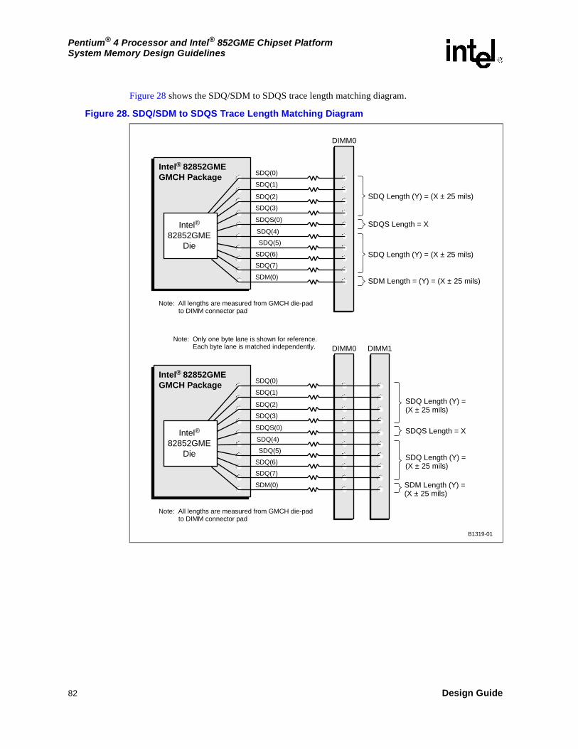
82 Design Guide
Pentium® 4 Processor and Intel® 852GME Chipset PlatformSystem Memory Design Guidelines
Figure 28 shows the SDQ/SDM to SDQS trace length matching diagram.
Figure 28. SDQ/SDM to SDQS Trace Length Matching Diagram
B1319-01
Intel® 82852GMEGMCH Package
SDQ Length (Y) = (X ± 25 mils)
SDQ(0)
SDQ(1)
SDQ(2)
SDQ(3)
SDQS(0)
SDQ(4)
SDQ(5)
SDQ(6)
SDQ(7)
SDM(0)
DIMM0
SDQ Length (Y) = (X ± 25 mils)
SDM Length = (Y) = (X ± 25 mils)
SDQS Length = XIntel®
82852GMEDie
DIMM1
Note: All lengths are measured from GMCH die-pad to DIMM connector pad
Note: Only one byte lane is shown for reference. Each byte lane is matched independently.
Intel® 82852GMEGMCH Package
SDQ Length (Y) =(X ± 25 mils)
SDQ Length (Y) =(X ± 25 mils)
SDQ(0)
SDQ(1)
SDQ(2)
SDQ(3)
SDQS(0)
SDQ(4)
SDQ(5)
SDQ(6)
SDQ(7)
SDM(0)
DIMM0
SDM Length (Y) =(X ± 25 mils)
SDQS Length = XIntel®
82852GMEDie
Note: All lengths are measured from GMCH die-pad to DIMM connector pad

Design Guide 83
Pentium® 4 Processor and Intel® 852GME Chipset PlatformSystem Memory Design Guidelines
6.4.4.5 SDQ/SDQS Signal Package Lengths
Use the package length data in Table 27 to tune the length of each SDQ, SDM, and SDQS motherboard trace to achieve the overall length matching requirements defined in the prior sections.
Table 27. DDR SDQ/SDM/SDQS Package Lengths (Sheet 1 of 2)
Signal Pin Number Pkg Length (mils) Signal Pin Number Pkg Length
(mils)
SDQ[0] AF2 785 SDQ[32] AH16 766
SDQ[1] AE3 751 SDQ[33] AG17 558
SDQ[2] AF4 690 SDQ[34] AF19 510
SDQ[3] AH2 903 SDQ[35] AE20 579
SDQ[4] AD3 682 SDQ[36] AD18 408
SDQ[5] AE2 739 SDQ[37] AE18 458
SDQ[6] AG4 741 SDQ[38] AH18 658
SDQ[7] AH3 845 SDQ[39] AG19 596
SDQ[8] AD6 607 SDQ[40] AH20 677
SDQ[9] AG5 756 SDQ[41] AG20 730
SDQ[10] AG7 685 SDQ[42] AF22 562
SDQ[11] AE8 558 SDQ[43] AH22 702
SDQ[12] AF5 734 SDQ[44] AF20 563
SDQ[13] AH4 825 SDQ[45] AH19 644
SDQ[14] AF7 644 SDQ[46] AH21 716
SDQ[15] AH6 912 SDQ[47] AG22 783
SDQ[16] AF8 622 SDQ[48] AE23 592
SDQ[17] AG8 624 SDQ[49] AH23 752
SDQ[18] AH9 676 SDQ[50] AE24 666
SDQ[19] AG10 634 SDQ[51] AH25 817
SDQ[20] AH7 710 SDQ[52] AG23 639
SDQ[21] AD9 508 SDQ[53] AF23 667
SDQ[22] AF10 569 SDQ[54] AF25 707
SDQ[23] AE11 469 SDQ[55] AG25 783
SDQ[24] AH10 648 SDQ[56] AH26 834
SDQ[25] AH11 622 SDQ[57] AE26 701
SDQ[26] AG13 572 SDQ[58] AG28 808
SDQ[27] AF14 655 SDQ[59] AF28 756
SDQ[28] AG11 599 SDQ[60] AG26 782

84 Design Guide
Pentium® 4 Processor and Intel® 852GME Chipset PlatformSystem Memory Design Guidelines
SDQ[29] AD12 460 SDQ[61] AF26 748
SDQ[30] AF13 536 SDQ[62] AE27 673
SDQ[31] AH13 642 SDQ[63] AD27 608
SDQ[64] AG14 566
SDQ[65] AE14 477
SDQ[66] AE17 571
SDQ[67] AG16 530
SDQ[68] AH14 701
SDQ[69] AE15 421
SDQ[70] AF16 491
SDQ[71] AF17 530
SDQS[0] AG2 925 SDM[0] AE5 838
SDQS[1] AH5 838 SDM[1] AE6 693
SDQS[2] AH8 756 SDM[2] AE9 538
SDQS[3] AE12 466 SDM[3] AH12 606
SDQS[4] AH17 678 SDM[4] AD19 492
SDQS[5] AE21 487 SDM[5] AD21 470
SDQS[6] AH24 770 SDM[6] AD24 557
SDQS[7] AH27 858 SDM[7] AH28 917
SDQS[8] AD15 418 SDM[8] AH15 685
Table 27. DDR SDQ/SDM/SDQS Package Lengths (Sheet 2 of 2)
Signal Pin Number Pkg Length (mils) Signal Pin Number Pkg Length
(mils)
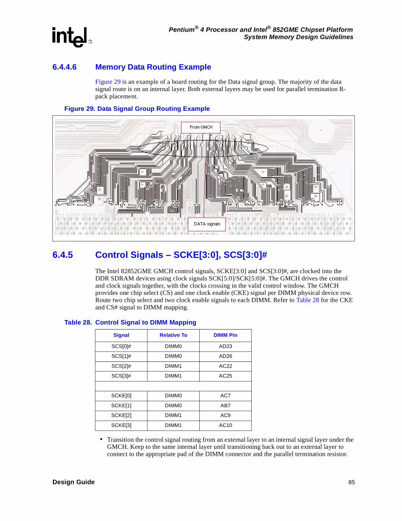
Design Guide 85
Pentium® 4 Processor and Intel® 852GME Chipset PlatformSystem Memory Design Guidelines
6.4.4.6 Memory Data Routing Example
Figure 29 is an example of a board routing for the Data signal group. The majority of the data signal route is on an internal layer. Both external layers may be used for parallel termination R-pack placement.
6.4.5 Control Signals – SCKE[3:0], SCS[3:0]#
The Intel 82852GME GMCH control signals, SCKE[3:0] and SCS[3:0]#, are clocked into the DDR SDRAM devices using clock signals SCK[5:0]/SCK[5:0]#. The GMCH drives the control and clock signals together, with the clocks crossing in the valid control window. The GMCH provides one chip select (CS) and one clock enable (CKE) signal per DIMM physical device row. Route two chip select and two clock enable signals to each DIMM. Refer to Table 28 for the CKE and CS# signal to DIMM mapping.
• Transition the control signal routing from an external layer to an internal signal layer under the GMCH. Keep to the same internal layer until transitioning back out to an external layer to connect to the appropriate pad of the DIMM connector and the parallel termination resistor.
Figure 29. Data Signal Group Routing Example
Table 28. Control Signal to DIMM Mapping
Signal Relative To DIMM Pin
SCS[0]# DIMM0 AD23
SCS[1]# DIMM0 AD26
SCS[2]# DIMM1 AC22
SCS[3]# DIMM1 AC25
SCKE[0] DIMM0 AC7
SCKE[1] DIMM0 AB7
SCKE[2] DIMM1 AC9
SCKE[3] DIMM1 AC10
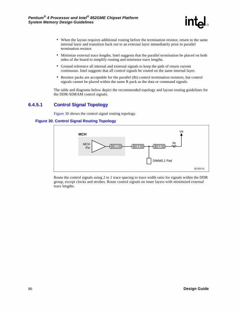
86 Design Guide
Pentium® 4 Processor and Intel® 852GME Chipset PlatformSystem Memory Design Guidelines
• When the layout requires additional routing before the termination resistor, return to the same internal layer and transition back out to an external layer immediately prior to parallel termination resistor.
• Minimize external trace lengths. Intel suggests that the parallel termination be placed on both sides of the board to simplify routing and minimize trace lengths.
• Ground reference all internal and external signals to keep the path of return current continuous. Intel suggests that all control signals be routed on the same internal layer.
• Resistor packs are acceptable for the parallel (Rt) control termination resistors, but control signals cannot be placed within the same R pack as the data or command signals.
The table and diagrams below depict the recommended topology and layout routing guidelines for the DDR-SDRAM control signals.
6.4.5.1 Control Signal Topology
Figure 30 shows the control signal routing topology.
Route the control signals using 2 to 1 trace spacing to trace width ratio for signals within the DDR group, except clocks and strobes. Route control signals on inner layers with minimized external trace lengths.
Figure 30. Control Signal Routing Topology
B1320-01
Rt
Vtt
MCHPin
MCH
DIMM0,1 Pad
L1P1 L2

Design Guide 87
Pentium® 4 Processor and Intel® 852GME Chipset PlatformSystem Memory Design Guidelines
6.4.5.2 Control Signal Routing Guidelines
Table 29 presents the control signal routing guidelines.
Table 29. Control Signal Routing Guidelines
Parameter Routing Guidelines
Signal group SCKE[3:0], SCS[3:0]#
Motherboard topology Point-to-point with parallel termination
Reference plane Ground referenced
Characteristic trace impedance (Zo) 55 Ω ± 15%
Nominal trace widthInner layers: 4 mils
Outer layers: 5 mils
Minimum spacing to trace width ratio 2 to 1 (for example, 8 mil space to 4 mil trace)
Minimum isolation spacing to non-DDR signals 20 mils
Package length P1500 mils ± 250 mils
See Table 30 for exact lengths.
Trace length P1+ L1 – GMCH control signal ball to DIMM pad
Min = 2.0 inches
Max = 6.0 inches
Trace length L2 – DIMM pad to parallel termination resistor pad
Max = 2.0 inches
Parallel termination resistor (Rt) 56 Ω ± 5%
Maximum recommended motherboard via count per signal
3
Length matching requirementsMatch CTRL to SCK[5:0]/SCK[5:0]#
See Section 6.4.5.3 and Figure 31.
NOTES:1. Recommended resistor values and trace lengths may change in a later revision of the design guide.2. Power distribution vias from Rt to Vtt are not included in this count.3. It is possible to route using two vias if one via is shared that connects to the DIMM pad and parallel
termination resistor.4. The overall maximum and minimum length to the DIMM must comply with clock length matching
requirements.

88 Design Guide
Pentium® 4 Processor and Intel® 852GME Chipset PlatformSystem Memory Design Guidelines
6.4.5.3 Control to Clock Length Matching Requirements
The length of the control signals between the GMCH die pad and the DIMM must fall within the range defined below with respect to the associated clock reference length. Refer to Figure 30 for a definition of the various trace segments that make up this path. The length of trace from the DIMM to the termination resistor need not be length matched. The length matching requirements are also shown in Figure 31.
Length range formula for DIMM0:
X0 = SCK[2:0]/SCK[2:0]# total reference length, including package length.
See Section 6.4.3.2.
Y0 = SCS[1:0]# & SCKE[1:0] total length = GMCH package length + L1, as
shown in Figure 31, where:
(X0 – 1.5”) ≤ Y0 ≤ (X0 - 0.5”)
Length range formula for DIMM1:
X1 = SCK[5:3]/SCK[5:3]# total reference length, including package length.
See Section 6.4.3.2.
Y1 = SCS[3:2]# & SCKE[3:2] total length = GMCH package length + L1, as
shown in Figure 31, where:
(X1 – 1.5”) ≤ Y1 ≤ (X1 - 0.5”)
No length matching is required from the DIMM to the termination resistor. Figure 31 shows the length matching requirements between the control signals and clock. A nominal CS/CKE package length of 500 mils may be used to estimate baseline MB lengths.

Design Guide 89
Pentium® 4 Processor and Intel® 852GME Chipset PlatformSystem Memory Design Guidelines
Figure 31 shows the control signal to clock trace length matching diagram.
Figure 31. Control Signal to Clock Trace Length Matching Diagram
B1317-02
DIMM0
Intel® 82852GMEGMCH Package
SDQS Length = Y0, where(X0 - 1.5") < Y0 < (X0 - 0.5")
Clock Reference Length = X0
SDQS[8:0]
SCK[2:0]
SCK#[2:0]
DIMM0
Intel 82852GMEGMCH Package
DIMM1
SDQS Length = Y1(X1 - 1.5") Y1 (X1 - 0.5")
Clock Reference Length = X1
SDQS[8:0]
SCK[5:3]
SCK#[5:3]
Note: All lengths are measured from GMCH die-pad to DIMM connector pad
Note: All lengths are measured from GMCH die-pad to DIMM connector pad
Intel®
82852GMEDie
Intel82852GME
Die

90 Design Guide
Pentium® 4 Processor and Intel® 852GME Chipset PlatformSystem Memory Design Guidelines
6.4.5.4 Control Group Package Length Table
Use the package length data in the Table 30 to match the overall length of each command signal to its associated clock reference length.
Note: Due to the relatively small variance in package length and adequate timing margins, it is acceptable to use a fixed 500 mil nominal package length for all control signals, thereby reducing the complexity of the motherboard length calculations.
Table 30. Control Group Package Lengths
Signal Pin Number Package Length (mils)
SCS[0]# AD23 502
SCS[1]# AD26 659
SCS[2]# AC22 544
SCS[3]# AC25 612
SCKE[0] AC7 443
SCKE[1] AB7 389
SCKE[2] AC9 386
SCKE[3] AC10 376

Design Guide 91
Pentium® 4 Processor and Intel® 852GME Chipset PlatformSystem Memory Design Guidelines
6.4.5.5 Control Topology Routing Example
Figure 32 is an example of a board routing for the Control signal group.
6.4.6 Command Signals – SMA[12:6,3,0], SBA[1:0], SRAS#, SCAS#, SWE#
The Intel 82852GME GMCH command signals, SMA[12:6,3,0], SBA[1:0], SRAS#, SCAS#, and SWE# clocked into the DDR SDRAMs using the clock signals SCK[5:0]/SCK[5:0]#. The GMCH drives the command and clock signals together, with the clocks crossing in the valid command window. The command signal group is supported by a daisy chain topology. This topology places a series resistor between the two DIMMs to dampen DIMM to DIMM resonance.
Transition the command signal routing from an external layer to an internal signal layer under the GMCH. Keep to the same internal layer until transitioning back to an external layer immediately prior to connecting the DIMM0 connector pad. At the via transition for DIMM0, continue the signal route on the same internal layer to the series termination resistor (Rs), collocated to DIMM1. At this resistor, transition the signal to an external layer immediately prior to the pad of Rs. After the series resistor, Rs, continue the signal route on the external layer landing on the appropriate connector pad of DIMM1. After DIMM1, transition to the same internal layer or stay on the external layer and route the signal to Rt.
Intel suggests that the parallel termination (Rt) be placed on both sides of the board to simplify routing and minimize trace lengths. Ground reference all internal and external signals to keep the path of the return current continuous.
Figure 32. Control Signal Group Routing Example

92 Design Guide
Pentium® 4 Processor and Intel® 852GME Chipset PlatformSystem Memory Design Guidelines
Resistor packs are acceptable for the series and parallel command termination resistors but command signals cannot be placed within the same R-packs as data, strobe, or control signals. The diagrams and tables below depict the recommended topology and layout routing guidelines for the DDR-SDRAM command signals routing to DIMM0 and DIMM1.
Figure 33 shows the command routing for topology.
Route the command signals using a 2 to 1 trace spacing to trace width ratio for signals within the DDR group, except clocks and strobes. Route command signals on inner layers with minimized external traces.
Figure 33. Command Routing for Topology
B1322-01
Rt
Vtt
MCHPin
MCH
DIMM0 Pad DIMM1 Pad
L1P1 L2 L3

Design Guide 93
Pentium® 4 Processor and Intel® 852GME Chipset PlatformSystem Memory Design Guidelines
6.4.6.1 Command Topology Routing Guidelines
Table 31 presents the command topology routing guidelines.
Table 31. Command Topology Routing Guidelines
Parameter Routing Guidelines
Signal group SMA[12:6,3,0], SBA[1:0], SRAS#, SCAS#, SWE#
Motherboard topology Daisy chain with parallel termination
Reference plane Ground referenced
Characteristic trace impedance (Zo) 55 Ω ± 15%
Nominal trace widthInner layers: 4 mils
Outer layers: 5 mils
Minimum spacing to trace width ratio 2 to 1 (for example, 8 mil space to 4 mil trace)
Minimum isolation spacing to non-DDR signals 20 mils
Package length P1500 mils ± 250 mils
See Section 32 for exact package lengths.
Trace length P1+ L1Min = 2.0 inches
Max = 5.5 inches
Trace length P1+ L1+L2+L3 Max = 7.5 inches
Trace length L2 – total DIMM to DIMM spacing Max = 2.0 inches
Trace length L3 – second DIMM pad to parallel resistor pad Max = 1.5 inches
Parallel termination resistor (Rt) 56 Ω ± 5%
Maximum recommended motherboard via count per signal 6
Length matching requirementsCMD to SCK/SCK#
See Section 6.4.6.1 and Figure 34 for details.
NOTES:1. Recommended resistor values and trace lengths may change in a later revision of the design guide.2. Power distribution vias from Rt to Vtt are not included in this count.3. The overall maximum and minimum length to the DIMM must comply with clock length matching
requirements.4. It is possible to route using four vias if one via is shared that connects to the DIMM1 pad and parallel
termination resistor.

94 Design Guide
Pentium® 4 Processor and Intel® 852GME Chipset PlatformSystem Memory Design Guidelines
6.4.6.2 Command Topology Length Matching Requirements
The routing length of the command signals between the GMCH die pad and the DIMM must be within the range defined below with respect to the associated clock reference length. Refer to Figure 33 for a definition of the various motherboard trace segments. The length of trace from the DIMM to the termination resistor need not be length matched.
Length range formula for DIMM0:
X0 = SCK[2:0]/SCK[2:0]# total reference length, including package length.
See Section 6.4.3.2.
Y0 = CMD signal total length = GMCH package + L1, as shown in Figure 34,
where:
(X0 – 1.5”) ≤ Y0 ≤ (X0 + 1.0”)
Length range formula for DIMM1:
X1 = SCK[5:3]/SCK[5:3]# total reference length, including package length.
See Section 6.4.3.2.
Y1 = CMD signal total length = GMCH package + L1 + L2 + L3, as shown in
Figure 34, where:
(X1 – 1.5”) ≤ Y1 ≤ (X1 + 1.0”)
No length matching is required from DIMM1 to the termination resistor. Figure 34 shows the length matching requirements between the command signals and clock. A nominal CMD package length of 500 mils may be used to estimate baseline MB lengths. Refer to Section 6.3 for more details on package length compensation.
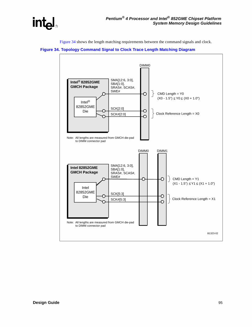
Design Guide 95
Pentium® 4 Processor and Intel® 852GME Chipset PlatformSystem Memory Design Guidelines
Figure 34 shows the length matching requirements between the command signals and clock.
Figure 34. Topology Command Signal to Clock Trace Length Matching Diagram
B1323-02
Intel® 82852GMEGMCH Package
CMD Length = Y0(X0 - 1.5") Y0 (X0 + 1.0")
Clock Reference Length = X0
SMA[12:6, 3:0],SBA[1:0],SRAS#, SCAS#,SWE#
SMA[12:6, 3:0],SBA[1:0],SRAS#, SCAS#,SWE#
SCK[2:0]
SCK#[2:0]
DIMM0
DIMM0
Intel 82852GMEGMCH Package
DIMM1
CMD Length = Y1(X1 - 1.5") Y1 (X1 + 1.0")
Clock Reference Length = X1
SCK[5:3]
SCK#[5:3]
Note: All lengths are measured from GMCH die-pad to DIMM connector pad
Note: All lengths are measured from GMCH die-pad to DIMM connector pad
Intel®
82852GMEDie
Intel82852GME
Die

96 Design Guide
Pentium® 4 Processor and Intel® 852GME Chipset PlatformSystem Memory Design Guidelines
6.4.6.3 Command Group Package Length Table
Use the package length data in Table 32 to match the overall length of each command signal to its associated clock reference length.
Table 32. Command Group Package Lengths
Signal Pin Number Pkg Length (mils)
SMA[0] AC18 420
SMA[3] AD17 472
SMA[6] AD8 591
SMA[7] AD7 596
SMA[8] AC6 630
SMA[9] AC5 681
SMA[10] AC19 377
SMA[11] AD5 683
SMA[12] AB5 609
SBA[0] AD22 592
SBA[1] AD20 435
SCAS# AC24 562
SRAS# AC21 499
SWE# AD25 751

Design Guide 97
Pentium® 4 Processor and Intel® 852GME Chipset PlatformSystem Memory Design Guidelines
6.4.6.4 Command Topology Routing Example
Figure 35 is an example of a board routing for the Command signal group.
6.4.7 CPC Signals – SMA[5,4,2,1], SMAB[5,4,2,1]
The Intel 82852GME GMCH control signals, SMA[5,4,2,1] and SMAB[5,4,2,1], are common clocked signals. They are clocked into the DDR SDRAM devices using clock signals SCK[5:0]/SCK[5:0]#. The GMCH drives the CPC and clock signals together, with the clocks crossing in the valid control window. The GMCH provides one set of CPC signals per DIMM slot. Refer to Table 33 for the SMA and SMAB signal to DIMM mapping.
Figure 35. Command Signal Group Routing Example
Table 33. Control Signal to DIMM Mapping (Sheet 1 of 2)
Signal Relative To DIMM Pin
SMA[1] DIMM0 AD14
SMA[2] DIMM0 AD13
SMA[4] DIMM1 AD11
SMA[5] DIMM1 AC13
SMAB[1] DIMM0 AD16
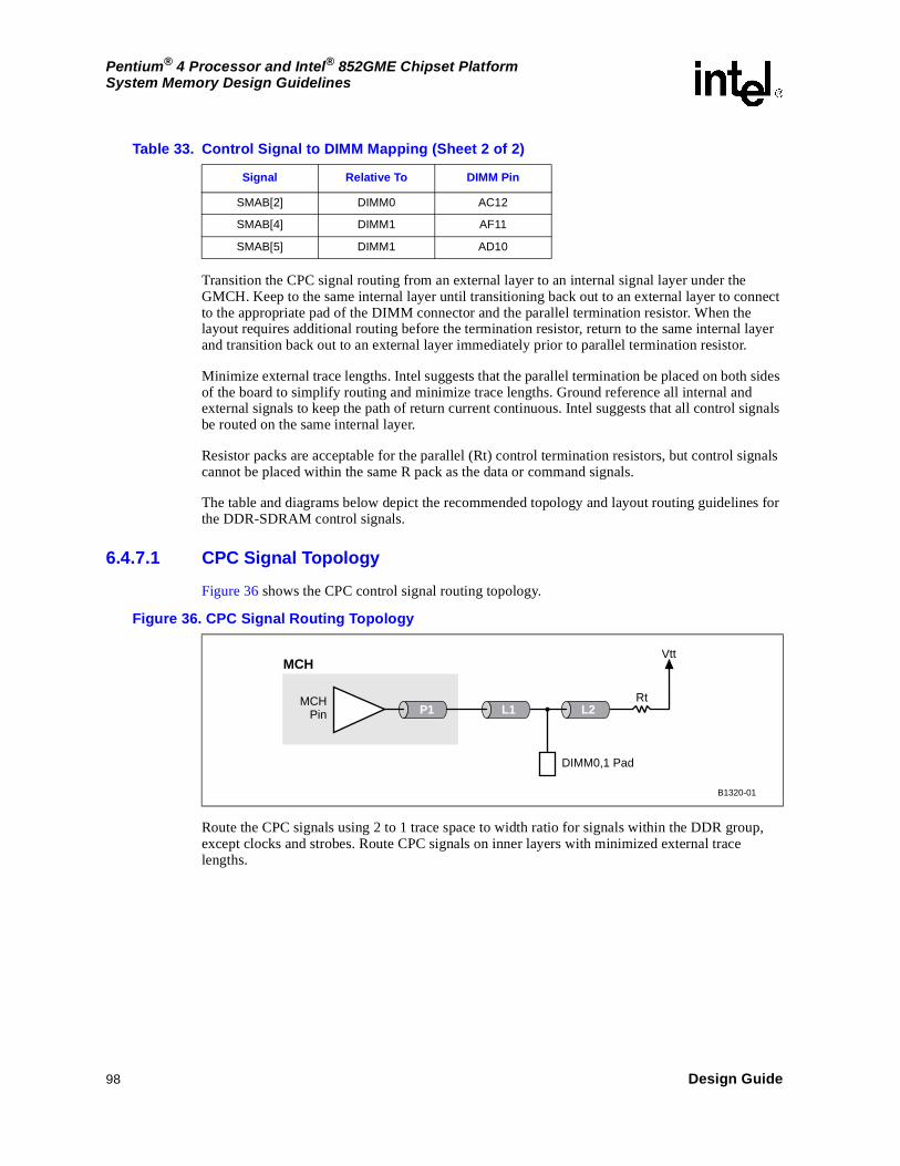
98 Design Guide
Pentium® 4 Processor and Intel® 852GME Chipset PlatformSystem Memory Design Guidelines
Transition the CPC signal routing from an external layer to an internal signal layer under the GMCH. Keep to the same internal layer until transitioning back out to an external layer to connect to the appropriate pad of the DIMM connector and the parallel termination resistor. When the layout requires additional routing before the termination resistor, return to the same internal layer and transition back out to an external layer immediately prior to parallel termination resistor.
Minimize external trace lengths. Intel suggests that the parallel termination be placed on both sides of the board to simplify routing and minimize trace lengths. Ground reference all internal and external signals to keep the path of return current continuous. Intel suggests that all control signals be routed on the same internal layer.
Resistor packs are acceptable for the parallel (Rt) control termination resistors, but control signals cannot be placed within the same R pack as the data or command signals.
The table and diagrams below depict the recommended topology and layout routing guidelines for the DDR-SDRAM control signals.
6.4.7.1 CPC Signal Topology
Figure 36 shows the CPC control signal routing topology.
Route the CPC signals using 2 to 1 trace space to width ratio for signals within the DDR group, except clocks and strobes. Route CPC signals on inner layers with minimized external trace lengths.
SMAB[2] DIMM0 AC12
SMAB[4] DIMM1 AF11
SMAB[5] DIMM1 AD10
Table 33. Control Signal to DIMM Mapping (Sheet 2 of 2)
Signal Relative To DIMM Pin
Figure 36. CPC Signal Routing Topology
B1320-01
Rt
Vtt
MCHPin
MCH
DIMM0,1 Pad
L1P1 L2

Design Guide 99
Pentium® 4 Processor and Intel® 852GME Chipset PlatformSystem Memory Design Guidelines
6.4.7.2 CPC Signal Routing Guidelines
Table 34 shows the CPC signal routing guidelines.
Table 34. CPC Signal Routing Guidelines
Parameter Routing Guidelines
Signal group SMA[5,4,2,1], SMAB[5,4,2,1]
Motherboard topology Point-to-point with parallel termination
Reference plane Ground referenced
Characteristic trace impedance (Zo) 55 Ω ± 15%
Nominal trace widthInner layers: 4 mils
Outer layers: 5 mils
Minimum spacing to trace width ratio 2 to 1 (for example, 8 mil space to 4 mil trace)
Minimum isolation spacing to non-DDR Signals 20 mils
Package length P1500 mils ± 250 mils
See Table 35 for exact lengths.
Trace length P1+ L1 Min = 2.0 inches
Max = 6.0 inches
Trace length L2 – DIMM pad to parallel termination resistor pad Max = 2.0 inches
Parallel termination resistor (Rt) 56 Ω ± 5%
Maximum recommended motherboard via count per signal 3
Length matching requirementsMatch CPC to SCK[5:0]/SCK[5:0]#
See Section 6.4.8.3 and Figure 37 for details.
NOTES:1. Recommended resistor values and trace lengths may change in a later revision of the design guide.2. Power distribution vias from Rt to Vtt are not included in this count.3. It is possible to route using two vias if one via is shared that connects to the DIMM pad and parallel
termination resistor.4. The overall maximum and minimum length to the DIMM must comply with clock length matching
requirements.

100 Design Guide
Pentium® 4 Processor and Intel® 852GME Chipset PlatformSystem Memory Design Guidelines
6.4.7.3 CPC to Clock Length Matching Requirements
The total length of the CPC signals between the GMCH die pad and the DIMM must fall within the range defined below with respect to the associated clock reference length. Refer to Figure 36 for a definition of the various trace segments. The length the trace from the DIMM to the termination resistor need not be length matched. The length matching requirements are also depicted in Figure 37. Table 35 provides CPC signal package length information.
Length range formula for DIMM0:
X0 = SCK[2:0]/SCK[2:0]# total reference length, including package length.
See Section 6.4.1.
Y0 = SMA[5,4,2,1] total length = L1, as shown in Section 6.4.3.2, where:
(X0 – 1.5”) ≤ Y0 ≤ (X0 - 0.5”)
Length range formula for DIMM1:
X1 = SCK[5:3]/SCK[5:3]# total reference length, including package length.
See Section 6.4.1.
Y1 = SMAB[5,4,2,1] total length = L1, as shown in Section 6.4.3.2, where:
(X1 – 1.5”) ≤ Y1 ≤ (X1 - 0.5”)
No length matching is required from DIMM1 to the termination resistor. Figure 37 shows the length matching requirements between the CPC signals and clock. A nominal CPC package length of 500 mils may be used to estimate baseline MB lengths.

Design Guide 101
Pentium® 4 Processor and Intel® 852GME Chipset PlatformSystem Memory Design Guidelines
Figure 37 shows the length matching requirements between the CPC signals and clock.
Figure 37. CPC Signals to Clock Length Matching Diagram
B1324-01
Intel® 82852GMEGMCH Package
CPC Length = Y0(X0 - 1.5") <= Y0 <= (X0 - 0.5")
Clock Reference Length = X0
SMA[5,4,2,1]
SMAB[5,4,2,1]
SCK[2:0]
SCK#[2:0]
DIMM0
DIMM0
Intel 82852GMEGMCH Package
DIMM1
CPC Length = Y1(X1 - 1.5") <= Y1 <= (X1 - 0.5")
Clock Reference Length = X1
SCK[5:3]
SCK#[5:3]
Note: All lengths are measured from GMCH die-pad to DIMM connector pad
Note: All lengths are measured from GMCH die-pad to DIMM connector pad
Intel®
82852GMEDie
Intel82852GME
Die

102 Design Guide
Pentium® 4 Processor and Intel® 852GME Chipset PlatformSystem Memory Design Guidelines
6.4.7.4 CPC Group Package Length Table
Use the package length data in Table 35 to match the overall length of each CPC signal to its associated clock reference length.
6.4.8 Feedback – RCVENOUT#, RCVENIN#
The Intel 82852GME GMCH provides a Receive Enable (RCVENIN#) feedback signal that is used to measure timing for memory read data. The Intel 852GME chipset has the RCVENOUT# signal shunted directly to RCVENIN# inside the package to reduce timing variation. With this change, it is no longer necessary to provide an external connection. However, Intel recommends that both signals be transitioned to the bottom side with vias located adjacent to the package ball to facilitate probing.
6.5 ECC Guidelines
The GMCH may be configured to operate in an ECC data integrity mode that allows multiple bit error detection and single bit error correction. This option to design for and support ECC DDR memory modules is dependent on design objectives. By default, ECC functionality is disabled on the platform.
6.5.1 Graphics Limitations Using ECC Memory
Memory with ECC enabled requires additional system memory resources. The Intel 852GME chipset supports UMA, and this will cause the integrated graphics engine to have less memory bandwidth for accessing graphics from the buffer. A system BIOS workaround is required to allow additional access time to memory. Contact your BIOS vendor for the latest update.
DIMMs with ECC enabled are supported under limited display configurations. Table 36 presents supported display configurations.
Table 35. CPC Group Package Lengths
Signal Pin Number Pkg Length (mils)
SMA[1] AD14 398
SMA[2] AD13 443
SMA[4] AD11 430
SMA[5] AC13 346
SMAB[1] AD16 427
SMAB[2] AC12 395
SMAB[4] AF11 716
SMAB[5] AD10 631

Design Guide 103
Pentium® 4 Processor and Intel® 852GME Chipset PlatformSystem Memory Design Guidelines
6.5.2 GMCH ECC Functionality
When non-ECC memory modules are to be the only supported memory type on the platform, the eight DDR check bits signals, associated strobe and data mask bit associated with the ECC device for each DIMM may be left as no connects on the GMCH.
Note: All three differential clocks per DDR DIMM must be routed and driven to each respective DIMM connector, regardless of ECC support.
For the GMCH, this includes SDQ[71:64], SDQS8, and SDM8.
Consult the latest revision of the latest revision of the RS-852GME Chipset GMCH BIOS Specification for more details on register programming routines
The DRAM Data Integrity Mode (DDIM) bit of the DRC register (Device 0; Offset 7C-7Fh; bit 21) provides the option to enable or disable ECC operation mode in the GMCH. By default, this bit is set to '0' and ECC functionality is disabled. In such a case, the SDQ[71:64] and SDQS8 pins of the GMCH may be left as no connects.
On platforms where ECC memory is supported, it is important that all relevant SDQ and SDQS signals to the DIMMs be disabled when the system is populated with only non-ECC or a combination of ECC and non-ECC memory.
Table 36. Supported Internal Graphics Display Configuration with ECC Enabled
Graphics Core Configuration Supported Frequency and Resolutions
Graphics Core (minimum frequency) 200 MHz
Memory (minimum frequency) 266 MHz
Display Usage Single/Dual independent display
Dual Pipe Independent (maximum display resolution) 800 x 600, 8 bits per pixel (bpp), 85 Hz (DCLK = 56.25 MHz) on CRT
Single Pipe (maximum display resolution)
1600 x 1200, 16 bpp, 60 Hz (DCLK = 162 MHz) on CRT
1600 x 1200, 16 bpp, 75Hz (DCLK = 202.5 MHz) on CRT
1600 x 1200, 16 bpp, 80 Hz (DCLK = 229.5 MHz) on CRT
1400 x 1050, 16 bpp, 60 Hz (DCLK = 108 MHz) on LVDS
LVDS Support Single channel 18-bit panel
Display Concurrency One plane per pipe + cursor + overlay
DVO Support Yes
SSC Support No

104 Design Guide
Pentium® 4 Processor and Intel® 852GME Chipset PlatformSystem Memory Design Guidelines
6.5.3 DRAM Clock Flexibility
The DRAM Clock Control Disable Register (DCLKDIS: I/O Address 2E-2Fh) and the DRAM Controller Power Management Control Register, bit 10, (PWRMG: I/O Address 68-6Bh) provides the capability to enable and disable the CS/CKE and SCK signals to unpopulated DIMMs. The GMCH provides the flexibility to route any differential clock pair to any SCK clock pair on the DIMMs provided that the BIOS enables/disables these clocks appropriately (i.e., the GMCH's SCK0 pair may be routed either to the DIMM's SCK0 pair or any other pair such as SCK1 or SCK2, etc.). By default, the enable/disable bits for the clock pairs are set to '1' and are disabled or tri-stated.

Design Guide 105
Pentium® 4 Processor and Intel® 852GME Chipset PlatformMiscellaneous Logic
Miscellaneous Logic 7
The Intel® 82801DB ICH4 (ICH4) requires additional external circuitry to function properly. Some of these functions include meeting timing specifications, buffering signals, and switching between power wells. This logic may be implemented through the use of the Glue Chip or discrete logic.
7.1 Glue Chip 4
To reduce the component count and BOM (Bill of Materials) cost of the ICH4 platform, Intel has developed and ASIC component that integrates miscellaneous platform logic into a single chip. The ICH4 Glue Chip is designed to integrate some or all of the following functions into a single device. By integrating much of the required glue logic into a single device, overall board cost may be reduced.
Features include:
• Dual, strapping, selectable feature sets
• Audio-disable circuit
• Mute audio circuit
• 5 V reference generation
• 5 V standby reference generation
• HD single color LED driver
• IDE reset signal generation / PCIRST# buffers
• PWROK (PWRGD_3V) signal generation
• Power sequencing/ BACKFEED_CUT
• Power supply turn on circuitry
• RSMRST# generation
• Voltage translation from DDC to VGA monitor
• HSYNC/VSYNC voltage translation to VGA monitor
• Tri-state buffers for test
• Extra GP logic gates
• Power LED drivers
• Flash FLUSH# / INIT# circuit
More information regarding this component is available from the vendors presented in Table 37 on the next page.
106 Design Guide
Pentium® 4 Processor and Intel® 852GME Chipset PlatformMiscellaneous Logic
7.2 Discrete Logic
As an alternative solution, discrete circuitry may be implemented into a design instead of using the Glue Chip.
Table 37. Glue Chip 4 Vendor Information
Vendor Contact Information Vendor Part Number
Philips Semiconductor http://www.semiconductors.philips.com PCA9504A
Fujitsu Microelectronics http://www.fujitsumicro.com MB87B302ABPD-G-ER
Design Guide 107
Pentium® 4 Processor and Intel® 852GME Chipset PlatformFront Side Bus Design Guidelines
Front Side Bus Design Guidelines 8
The Pentium® 4 processor is the first Intel processor with the Intel NetBurst® microarchitecture. The Pentium 4 processor utilizes Flip-Chip Pin Grid Array (FC-PGA2) package technology and plugs into a 478-pin, surface-mount, Zero Insertion Force (ZIF) socket, referred to as the mPGA478B socket. The Pentium 4 processor maintains full compatibility with IA-32 software. The Pentium 4 processor’s 400/533-MT/s Intel NetBurst microarchitecture front side bus (FSB) utilizes a split-transaction, deferred reply.
The following layout guidelines support designs using the Pentium 4 processor and the Intel® 852GME chipset. Due to on-die Rtt resistors on both the processor and the chipset, additional resistors do not need to be placed on the motherboard for most FSB signals. The exception to these are RESET# and BPM[5:0]# signals, which require a 51.1 Ω pull-up, and the BR0 signal, which requires 220 Ω ± 5% pull-up to Vtt on the processor end of the transmission line.
8.1 FSB Routing Guidelines
Table 38 presents and summarizes the layout recommendations for the Pentium 4 processor and expands on specific design issues and their recommendations.
Table 38. FSB Routing Summary for the Processor (Sheet 1 of 2)
Parameter Processor Routing Guidelines
Line-to-line spacing
Greater than or equal to 2:1 edge-to-edge spacing versus trace width for address and address strobes Greater than or equal to 2.5:1 edge-to-edge spacing versus trace width or greater for data and data strobes.
See Figure 38 and Figure 39 for illustrations of this recommendation.
Data line lengths(agent-to-agent spacing)
Data line length of 1.0 to 6.0 inches from pin to pin. Route data signals of the same source synchronous group to the same pad-to-pad length within ± 0.100 inches of the associated strobes. The pad is defined as the attach point of the silicon die to the package substrate. Length must be added to the system board to compensate for package length differences. Route signals in the same source synchronous group on the same layer and referenced to Vss.
DSTBn/p[3:0]#
Route a data strobe and its complement within ± 0.025 inch of the same pad-to-pad length. The pad is defined as the attach point of the silicon die to the package substrate. Length must be added to the system board to compensate for package length differences. Route DSTBn/p# on the same layer as their associated data group and referenced to Vss.
Address line lengths(agent-to-agent spacing)
Address line length of 1.0 to 6.0 inches from pin-to-pin address signals of the same source synchronous group should be routed to the same pad-to-pad length within ± 0.200 inch of the associated strobes. The pad is defined as the attach point of the silicon die to the package substrate. Length must be added to the system board to compensate for package length differences. A layer transition may occur if the reference plane remains the same (Vss) and the layers are of the same configuration (all stripline or all microstrip).

108 Design Guide
Pentium® 4 Processor and Intel® 852GME Chipset PlatformFront Side Bus Design Guidelines
This is the edge-to-edge trace spacing versus width. For address and address strobes; a trace spacing-to-width ratio of 2-to-1 ensures a low crosstalk coefficient (based on geometries defined in 8 layer reference stackup). For data and data strobes, a trace spacing to width ratio of 2.5 to 1 or greater (as shown in Figure 39) ensures a low crosstalk coefficient (based on geometries defined in 8 layer reference stackup). All the effects of crosstalk are difficult to simulate. A smaller ratio would have an unpredictable impact due to crosstalk.
ADSTBn/p[1:0]#
Route an address strobe and its complement within ± 0.200 inch of the same pad-to-pad length. The pad is defined as the attach point of the silicon die to the package substrate. Length must be added to the system board to compensate for package length differences. A layer transition may occur if the reference plane remains the same (Vss) and the layers are all of the same configuration (all stripline or all microstrip).
Common clock line lengths 2.0 to 6.0 inches
Topology Stripline
Routing priorities
Route all associated signals and strobes on the same layer for entire length of bus. Reference all signals to Vss. Ideally, layer changes should not occur for any signals. When a layer change must occur, the reference plane must be Vss and the layers must all be of the same configuration (all stripline or all microstrip for example).
Clock keepout zones Maintain a spacing requirement of 16-20 mils around all clocks.
Trace Impedance 55 Ω ± 15%
Source synchronous routing restrictions
There are no length-matching routing restrictions between (or within) either the source-synchronous data or address groups. As long as the strobe and associated line length routing guidelines are met for each group, there is no need to length-match between the groups. For example, one data group may be routed to the minimum allowable length while another data group could be routed to the maximum allowable length. Simulations have verified that the FSB functions correctly even under this extreme condition.
NOTE: Refer to the Intel® 852GME Chipset GMCH and Intel® 852PM Chipset MCH Datasheet for GMCH package dimensions and refer to the Intel® Pentium® 4 Processor Datasheet for processor package dimensions.
Figure 38. Cross-Sectional View of 2:1 Ratio
Table 38. FSB Routing Summary for the Processor (Sheet 2 of 2)
Parameter Processor Routing Guidelines
R e fe r e n c e P la n e
2 x t ra c e t ra c e
x

Design Guide 109
Pentium® 4 Processor and Intel® 852GME Chipset PlatformFront Side Bus Design Guidelines
8.1.1 Return Path Evaluation
The return path is the route current takes to return to its source. It may take a path through ground planes, power planes, other signals, integrated circuits, vias, VRMs, etc. Think of the return path as following a path of least resistance back to the original source. Discontinuities in the return path often have signal integrity and timing effects that are similar to the discontinuities in the signal conductor. Therefore, the return paths must be given similar considerations. A way to evaluate return path parasitic inductance is to draw a loop that traces the current from the driver through the signal conductor to the receiver, then back through the ground/power plane to the driver again. The smaller the area of the loop, the lower the parasitic inductance.
The following sets of return path rules apply:
• Always trace out the return current path and provide as much care to the return path as the path of the signal conductor.
• Decoupling capacitors do not adequately compensate for a plane split.
• Do not allow splits in the reference planes in the path of the return current.
• Do not allow routing of signals on the reference planes near FSB signals.
• Maintain VSS as a reference plane for all FSB signals.
• Do not route over via anti-pads or socket anti-pads.
8.2 OPTIMIZED/COMPAT# Topology for Intel® 852GME Platforms
The OPITIMIZED/COMPAT# pin tells the processor if the internal FSB signal impedance is set to 50 or 60 Ω. By connecting the processor’s OPTIMIZED/COMPAT# pin AE26 pin to GND, the internal FSB signal impedance is set to 50 Ω. By leaving the pin as NC, the internal FSB signal impedance is set to 60 Ω. For the platform to be compatible with the mobile Pentium 4 processor, this pin must be left as NC. If a platform is only used with the mobile Pentium 4 processor, then this pin can be connected to GND.
Figure 39. Cross-Sectional View of 2:5:1 Ratio
R e fe r e n c e P la n e
2 .5 x t ra c e t ra c e
x

110 Design Guide
Pentium® 4 Processor and Intel® 852GME Chipset PlatformFront Side Bus Design Guidelines
8.2.1 GTLREF Layout and Routing Recommendations
There are four AGTL+ GTLREF pins on the processor that are used to set the reference voltage level for the AGTL+ signals (GTLREF). Because all of these pins are connected inside the processor package, the GTLREF voltage must be supplied to only one of the four pins.
Figure 40 shows an example of GTLREF routing.
• The processor must have one dedicated voltage divider.
• Decouple the voltage divider with a 1µF capacitor.
• Keep the voltage divider within 1.5 inches of the GTLREF pin.
• Decouple the pin with a high-frequency capacitor (such as a 220 pF 603) as close to the pin as possible.
• Keep signal routing at least 10 mils separated from the GTLREF routes. Use at least a 7 mil trace for routing.
• Do not allow signal lines to use the GTLREF routing as part of their return path (that is, do not allow the GTLREF routing to create splits or discontinuities in the reference planes of the FSB signals).
8.3 Processor Configuration
This section provides more details for routing Pentium 4 processor-based systems. This information is preliminary and subject to change. Both recommendations and considerations are presented.
For proper operation of the Pentium 4 processor and the Intel 852GME chipset, it is necessary to meet the timing and voltage specifications of each component. The following recommendations are Intel’s best guidelines based on extensive simulation and experimentation that make assumptions, which may be different than an OEM's system design. The most accurate way to understand the signal integrity and timing of the FSB in your platform is by performing a comprehensive simulation analysis. It is conceivable that adjustments to trace impedance, line length, termination impedance, board stackup and other parameters may improve system performance.
Refer to the Intel® Pentium® 4 Processor Datasheet for a FSB signal list, signal types and definitions.
Figure 40. GTLREF Routing
B1445-01
VC C C PU
1 µ F 220 pF
T line
L1 = 1.5 inches m axim um
49.9 Ω± 1%
100 Ω± 1%
G T LR E F pin

Design Guide 111
Pentium® 4 Processor and Intel® 852GME Chipset PlatformFront Side Bus Design Guidelines
8.4 General Topology and Layout Guidelines
The following topology and layout guidelines are preliminary and subject to change. The guidelines are derived from empirical testing with preliminary Intel 852GME chipset package models.
8.4.1 Design Recommendations
This following subsections contain the design recommendations for the data, address, strobes, and common clock signals. For the following discussion, the pad is defined as the attach point of the silicon die to the package substrate.
8.4.1.1 Data
Route data signals of the same source-synchronous group to the same pad-to-pad length within ± 0.100 inch of the associated strobes. As a result, additional traces are added to some data nets on the system board in order for all trace lengths within the same data group to be the same length (± 0.100 inch) from the pad of the processor to the associated pad of the chipset.
Equation 2. Calculation to Determine Package Delta Addition to MotherboardLength for UP Systems
Refer to the Intel® 852GME Chipset GMCH and Intel® 852PM Chipset MCH Datasheet for GMCH package dimensions and refer to the Intel® Pentium® 4 Processor Datasheet for package dimensions.
8.4.1.2 Address
Address signals follow the same rules as data signals except they should be routed to the same pad-to-pad length within ± 0.200 inch of the associated strobes. Address signals may change layers if the reference plane remains Vss.
8.4.1.3 Strobe
Route a strobe and its complement to a length equal to their corresponding data group's mean pad-to-pad length ± 0.025 inch.
8.4.1.4 Common Clock
Route common clock signals to a minimum pin-to-pin motherboard length of 2.0 inches and a maximum motherboard length of 6.0 inches.
Route source synchronous groups and associated strobes on the same layer for the entire length of the bus. This results in a significant reduction of the flight time skew since the dielectric thickness, line width, and velocity of the signals will be uniform across a single layer of the stackup. A relationship of dielectric thickness, line width, and velocity between layers cannot be ensured.
* Strobe package length is the average of the strobe pair.
deltanet,strobe cpu_pkglennet cpu_pkglenstrobe*–( ) cs_pkglennet cs_pkglenstrobe–( )+=

112 Design Guide
Pentium® 4 Processor and Intel® 852GME Chipset PlatformFront Side Bus Design Guidelines
Figure 41 shows the processor topology.
8.4.2 Source Synchronous (SS) Signals
Table 39 presents the FSB data signal routing guidelines. Table 40 presents the FSB address signal routing guidelines.
Figure 41. Processor Topology
B1326-01
Length L1
Pad
Processor Intel® 82852GMEGMCH
Pad
Legend:
Package TraceMotherboard PCB Trace
Table 39. FSB Data Signal Routing Guidelines
Signal Names Transmission Line Type Total Trace Length
Nominal Impedance
(Ω)
Width and Spacing
(mils)
CPU GMCH Min. (inches)
Max. (inches)
DBI[3:0]# DINV[3:0]# stripline 1.0 6.0 55 ± 15% 4.5 and 11.5
D[63:0]# HD[63:0]# stripline 1.0 6.0 55 ± 15% 4.5 and 11.5
DSTBN[3:0]# HDSTBN[3:0]# stripline 1.0 6.0 55 ± 15% 4.5 and 11.5
DSTBP[3:0]# HDSTBP[3:0]# stripline 1.0 6.0 55 ± 15% 4.5 and 11.5
NOTE: The data signals within each group must be routed to within ± 0.100 inch of its associated reference strobe. The complement strobe must be routed to within ± 0.025 inch of the associate reference strobe. All traces within each signal group must be routed on the same layer (required). Intel recommends that length of the strobes be centered to the average length of associated data or address traces to maximize setup/hold time margins.
Table 40. FSB Address Signal Routing Guidelines
Signal NamesTransmission
Line Type
Total Trace LengthNominal
Impedance (Ω)
Width and Spacing
(mils)CPU GMCH Min. (inches)
Max. (inches)
A[31:3]# HA[31:3]# Stripline 1.0 6.0 55 ± 15% 4.5 and 9
REQ[4:0]# HREQ[4:0]# Stripline 1.0 6.0 55 ± 15% 4.5 and 9
ADSTB[1:0]# HADSTB[1:0]# Stripline 1.0 6.0 55 ± 15% 4.5 and 9
NOTE: The address signals within each group must be routed to within ± 0.200 inch of its associated strobe. All traces within each signal group must be routed on the same layer (required). Intel recommends that length of the strobes be centered to the average length of associated data or address traces to maximize setup/hold time margins.
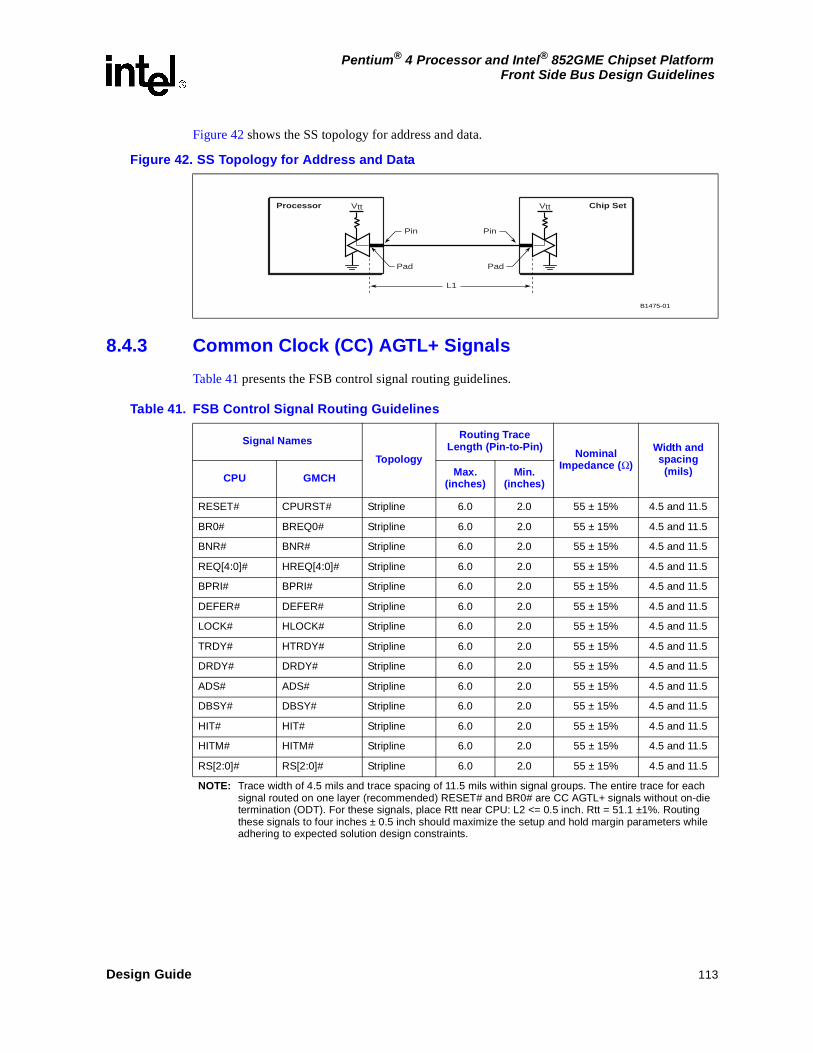
Design Guide 113
Pentium® 4 Processor and Intel® 852GME Chipset PlatformFront Side Bus Design Guidelines
Figure 42 shows the SS topology for address and data.
8.4.3 Common Clock (CC) AGTL+ Signals
Table 41 presents the FSB control signal routing guidelines.
Figure 42. SS Topology for Address and Data
B1475-01
Vtt
Pin
Pad Pad
L1
Pin
Processor Vtt Chip Set
Table 41. FSB Control Signal Routing Guidelines
Signal Names
Topology
Routing Trace Length (Pin-to-Pin)
Nominal Impedance (Ω)
Width and spacing (mils)
CPU GMCH Max. (inches)
Min. (inches)
RESET# CPURST# Stripline 6.0 2.0 55 ± 15% 4.5 and 11.5
BR0# BREQ0# Stripline 6.0 2.0 55 ± 15% 4.5 and 11.5
BNR# BNR# Stripline 6.0 2.0 55 ± 15% 4.5 and 11.5
REQ[4:0]# HREQ[4:0]# Stripline 6.0 2.0 55 ± 15% 4.5 and 11.5
BPRI# BPRI# Stripline 6.0 2.0 55 ± 15% 4.5 and 11.5
DEFER# DEFER# Stripline 6.0 2.0 55 ± 15% 4.5 and 11.5
LOCK# HLOCK# Stripline 6.0 2.0 55 ± 15% 4.5 and 11.5
TRDY# HTRDY# Stripline 6.0 2.0 55 ± 15% 4.5 and 11.5
DRDY# DRDY# Stripline 6.0 2.0 55 ± 15% 4.5 and 11.5
ADS# ADS# Stripline 6.0 2.0 55 ± 15% 4.5 and 11.5
DBSY# DBSY# Stripline 6.0 2.0 55 ± 15% 4.5 and 11.5
HIT# HIT# Stripline 6.0 2.0 55 ± 15% 4.5 and 11.5
HITM# HITM# Stripline 6.0 2.0 55 ± 15% 4.5 and 11.5
RS[2:0]# RS[2:0]# Stripline 6.0 2.0 55 ± 15% 4.5 and 11.5
NOTE: Trace width of 4.5 mils and trace spacing of 11.5 mils within signal groups. The entire trace for each signal routed on one layer (recommended) RESET# and BR0# are CC AGTL+ signals without on-die termination (ODT). For these signals, place Rtt near CPU: L2 <= 0.5 inch. Rtt = 51.1 ±1%. Routing these signals to four inches ± 0.5 inch should maximize the setup and hold margin parameters while adhering to expected solution design constraints.
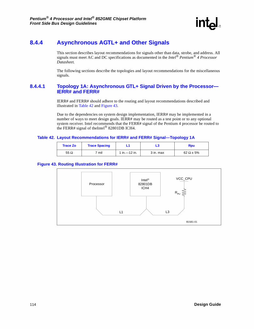
114 Design Guide
Pentium® 4 Processor and Intel® 852GME Chipset PlatformFront Side Bus Design Guidelines
8.4.4 Asynchronous AGTL+ and Other Signals
This section describes layout recommendations for signals other than data, strobe, and address. All signals must meet AC and DC specifications as documented in the Intel® Pentium® 4 Processor Datasheet.
The following sections describe the topologies and layout recommendations for the miscellaneous signals.
8.4.4.1 Topology 1A: Asynchronous GTL+ Signal Driven by the Processor—IERR# and FERR#
IERR# and FERR# should adhere to the routing and layout recommendations described and illustrated in Table 42 and Figure 43.
Due to the dependencies on system design implementation, IERR# may be implemented in a number of ways to meet design goals. IERR# may be routed as a test point or to any optional system receiver. Intel recommends that the FERR# signal of the Pentium 4 processor be routed to the FERR# signal of theIntel® 82801DB ICH4.
Table 42. Layout Recommendations for IERR# and FERR# Signal—Topology 1A
Trace Zo Trace Spacing L1 L3 Rpu
55 Ω 7 mil 1 in.—12 in. 3 in. max 62 Ω ± 5%
Figure 43. Routing Illustration for FERR#
B1581-01
ProcessorIntel®
82801DBICH4
L1
VCC_CPU
RPU
L3

Design Guide 115
Pentium® 4 Processor and Intel® 852GME Chipset PlatformFront Side Bus Design Guidelines
8.4.4.2 Topology 1B: Asynchronous GTL+ Signal Driven by the Processor—PROCHOT#
PROCHOT# should adhere to the routing and layout recommendations described and illustrated in Table 43 and Figure 44. When PROCHOT# is routed to external logic, voltage translation may be required to avoid excessive voltage levels at the processor and meet input thresholds for the external logic.
Table 43. Layout Recommendations for PROCHOT# Signal—Topology 1B
Trace Zo Trace Spacing L1 L2 L3 Rpu
55 Ω 7 mil 1 in.—17 in. 10 in. max 3 in. max 62 Ω ± 5%
Figure 44. Routing Illustration for PROCHOT#
Processor Voltage
Translator External
Logic
L2 = 10"
L1 L3
VCC_CPU
Rpu
Pro_Therm_Routi

116 Design Guide
Pentium® 4 Processor and Intel® 852GME Chipset PlatformFront Side Bus Design Guidelines
8.4.4.3 Topology 1C: Asynchronous GTL+ Signal Driven by the Processor—THERMTRIP#
THERMTRIP# should adhere to the routing and layout recommendations described and illustrated in Table 44 and Figure 45. When THERMTRIP# is routed to external logic, voltage translation may be required to avoid excessive voltage levels at the processor and meet input thresholds for the external logic.
Table 44. Layout Recommendations for THERMTRIP# Signal—Topology 1C
Trace Zo Trace Spacing L1 L3 Rpu
55 Ω 7 mil 1 in.—12 in. 3 in. max 62 Ω +/- 5%
Figure 45. Routing Illustration for THERMTRIP#
B1336-01
Rpu
Vcc
L3L1
ProcessorIntel®
82801DBICH4

Design Guide 117
Pentium® 4 Processor and Intel® 852GME Chipset PlatformFront Side Bus Design Guidelines
8.4.4.4 Topology 2A: Asynchronous GTL+ Signals Driven by theIntel® 82801DB ICH4—A20M#, IGNNE#, LINT[1:0], SLP#,SMI#, and STPCLK#
The Topology 2A CMOS A20M#, IGNNE#, LINT0/INTR, LINT1/NMI, SLP#, SMI#, and STPCLK# signals should implement a point-to-point connection between the ICH4 and the Pentium 4 processor. The routing guidelines allow both signals to be routed as either microstrip or strip lines using 55 Ω ± 15% characteristic trace impedance. No additional motherboard components are necessary for this topology. See Table 45 and Figure 46 for more information.
Table 45. Layout Recommendations for Topology 2A
L1 Transmission Line Type
0.5” - 12.0” Microstrip
0.5” - 12.0” Stripline
Figure 46. Routing Illustration Topology 2A
B1548-01
CPUIntel®
82801DBICH4
L1

118 Design Guide
Pentium® 4 Processor and Intel® 852GME Chipset PlatformFront Side Bus Design Guidelines
8.4.4.5 Topology 2B: Asynchronous GTL+ Signal Driven by theIntel® 82801DB ICH4—INIT#
INIT# should adhere to the routing and layout recommendations described and illustrated in Table 46 and Figure 47.
Level shifting is required for the INIT# signal to the FWH to meet input logic levels of the FWH.
Figure 48 illustrates one method of level shifting.
Table 46. Layout Recommendations for INIT#—Topology 2B
Trace Zo Trace Spacing L1 L2 L4 L5 Rpu
55 Ω 7 mils 2 in. max 10 in. max 17 in. max 3 in. max 330 Ω 5%
Figure 47. Routing Illustration for INIT#
B1338-02
Processor
FWH
Intel®
82801DBICH4
VoltageTransistorL4 L1
L2L5
330 Ω ± 5%
VCC_FWH
Figure 48. Voltage Translation of INIT#
B1339-01
INIT# fromIntel® 82801DB
ICH4
4.7 kΩ
INIT# to FWH
4.7 kΩ
12 V

Design Guide 119
Pentium® 4 Processor and Intel® 852GME Chipset PlatformFront Side Bus Design Guidelines
8.4.4.6 Topology 2C: Miscellaneous Signal Drivenby the Intel® 82801DB ICH4 Open Drain—PWRGOOD
PWRGOOD should adhere to the routing and layout recommendations described and illustrated in Table 47 and Figure 49.
8.4.4.7 Topology 3: VCCIOPLL, VCCA and VSSA
VCCIOPLL and VCCA are isolated power for internal PLLs. It is critical that they have clean, noiseless power on their input pins. See Section 4.1.2. for further details.
8.4.4.8 Topology 4: BR0# and RESET#
Since the processor does not have on-die termination on the BR0# and RESET# signals, it is necessary to terminate the signals using discrete components on the system board. Connect the signals between the components as shown in Figure 50. The Intel 852GME chipset has on-die termination; therefore, it is necessary to terminate only at the processor end. The value of Rt should be 51 Ω ± 5% for RESET#. BR0 signal requires 220 Ω + 5% pull-up to Vtt on the processor end of the transmission line.
Table 47. Layout Recommendations for Miscellaneous Signals—Topology 2C
Trace Zo Trace Spacing L1 L3 Rpu
55 Ω 7 mil 1 in.–12 in. 3 in. max 300 Ω ± 5%
Figure 49. Routing Illustration for PWRGOOD
B1340-01
ProcessorIntel®
82801DBICH4
L1L3
RPU
VCC_CPU
Figure 50. Routing Illustration for BR0# and RESET#
B1341-01
ProcessorIntel®
82801DBICH4
RPU
VCC_CPU
120 Design Guide
Pentium® 4 Processor and Intel® 852GME Chipset PlatformFront Side Bus Design Guidelines
8.4.4.9 Topology 5: COMP[1:0] Signals
The Pentium 4 processor has two COMP[1:0] pins, and the Intel 82852GME GMCH has two pins, HXRCOMP and HYRCOMP, that require compensation resistors to adjust the AGTL+IO buffer characteristics to specific board and operating environment characteristics.
Terminate the COMP[1:0] pins to ground through a 51 Ω ± 1% resistor as close as possible to the pin. Do not wire COMP pins together; connect each pin to its own termination resistor. RCOMP value may be adjusted to set external drive strength of I/O and to control the edge rate.
8.4.4.10 Topology 6: THERMDA/THERMDC Routing Guidelines
The processor incorporates an on-die thermal diode. THERMDA (diode anode) and THERMDC (diode cathode) pins on the processor can be connected to a thermal sensor located on the system board to monitor the die temperature of the processor for thermal management/long-term die temperature change monitoring purpose. This thermal diode is separate from the thermal monitor's thermal sensor and cannot be used to predict the behavior of the thermal monitor.
Since the thermal diode is used to measure a very small voltage from the remote sensor, take care to minimize noise induced at the sensor inputs. The following are some guidelines:
• Place the remote sensor as close as possible to THERMDA/THERMDC pins. It may be approximately four to eight inches away as long as the worst noise sources such as clock generators, data buses, and address buses, etc., are avoided.
• Route the THERMDA and THERMDC lines in parallel and close together with ground guards enclosed.
• Use wide tracks to reduce inductance and noise pickup that may be introduced by narrow ones. Intel recommends a width of 10 mils and spacing of 10 mils.
8.4.4.11 Topology 7: TESTHI Pins
Tie the TESTHI pins to the processor VCC using a matched resistor, where a matched resistor has a resistance value within ± 20% of the impedance of the board transmission line traces. For example, if the trace impedance is 50 Ω, then a value between 40 Ω and 60 Ω is required.
The TESTHI pins may use individual pull-up resistors or be grouped together as detailed below. Use a matched resistor for each group:
1. TESTHI[1:0]
2. TESTHI[7:2]
3. TESTHI[10:8]
4. TESTHI[12:11]
Additionally, if the ITPCLKOUT[1:0] pins are not used then they may be connected individually to VCC using matched resistors or grouped with TESTHI[5:2] with a single matched resistor. When they are being used, individual termination with 1 kΩ resistors is acceptable. Tying ITPCLKOUT[1:0] directly to VCC or sharing a pull-up resistor to VCC prevents the use of debug interposers. This implementation is strongly discouraged for system boards that do not implement an onboard debug port.

Design Guide 121
Pentium® 4 Processor and Intel® 852GME Chipset PlatformFront Side Bus Design Guidelines
As an alternative, group 2 (TESTHI [5:2]), and the ITPCLKOUT[1:0] pins may be tied directly to the processor VCC. This has no impact on system functionality. TESTHI[0] and TESTHI[12] may also be tied directly to processor VCC if resistor termination is a problem, but matched resistor termination is recommended. In the case of the ITPCLKOUT[1:0], direct tie to VCC is strongly discouraged for system boards that do not implement an onboard debug port.
8.5 Additional Processor Design Considerations
This section documents system design considerations not addressed in previous sections.
8.5.1 Retention Mechanism Placement and Keepouts
The Retention Mechanism (RM) requires a keep-out zone for a limited component height area under the RM as shown in Figure 51 and Figure 52. The figures show the relationship between the RM mounting holes and pin one of the socket. They also document the keepouts.
The retention holes should be non-plated with primary and secondary side route keepout area of 0.409 inches diameter.
For heat sink volumetric information refer to:
• Intel® Pentium® 4 Processor in the 478-pin package Thermal Design Guidelines
• Intel® Pentium® 4 Processor and Intel® Celeron® Processor in the 478-pin package Thermal Design Guide for Embedded Applications.

122 Design Guide
Pentium® 4 Processor and Intel® 852GME Chipset PlatformFront Side Bus Design Guidelines
Figure 51. Retention Mechanism Keep-Out Drawing 1
NOTE: Dimensions are in millimeters with inch dimensions in brackets.

Design Guide 123
Pentium® 4 Processor and Intel® 852GME Chipset PlatformFront Side Bus Design Guidelines
Figure 52. Retention Mechanism Keep-Out Drawing 2
NOTE: Dimensions are in millimeters with inch dimensions in brackets.

124 Design Guide
Pentium® 4 Processor and Intel® 852GME Chipset PlatformFront Side Bus Design Guidelines
8.5.2 Power Header for Active Cooling Solutions
The Intel reference-design heatsink includes an integrated fan. The recommended connector for the active cooling solution is a Walden*/Molex* 22-01-3037, AMP* 643815-3, or equivalent. The integrated fan requires the system board to supply a minimum of 740 mA at 12 V for proper operation. Table 48 presents the reference solution fan power header pinout.
The Intel boxed processor heatsink includes an integrated fan. The recommended connector for the active cooling solution is a Walden*/Molex* 22-23-2037, AMP* 640456-3 or equivalent. The integrated fan requires the system board to supply a minimum of 740 mA at 12 V for proper operation. Table 49 presents the boxed processor fan power header pinout.
The fan heatsink outputs a SENSE signal that is an open-collector output that pulses at a rate of two pulses per fan revolution. The system board requires a pull-up resistor to provide the appropriate Voh level to match the fan speed monitor. Use of the SENSE signal is optional. Tie pin 3 to ground when the SENSE signal is not used.
For more information on boxed processor requirements, refer to the Intel® Pentium® 4 Processor in the 478 Pin Package Datasheet.
8.6 Debug Port Routing Guidelines
Refer to the latest revision of the ITP700 Debug Port Design Guide for details on the implementation of the debug port. The document can be found from http://developer.intel.com/design/Xeon/guides/249679.htm
8.6.1 Debug Tools Specifications
8.6.1.1 Logic Analyzer Interface (LAI)
Intel is working with two logic analyzer vendors to provide logic analyzer interfaces (LAIs) for use in debugging the Pentium 4 processor systems. Contact Tektronix, Inc.* and Agilent Technologies, Inc.* for specific information about their LAIs. The following information is general in nature. Specific information must be obtained from the logic analyzer vendor.
Table 48. Reference Solution Fan Power Header Pinout
Pin Number Signal
1 Ground
2 +12 V
3 No Connect
Table 49. Boxed Processor Fan Power Header Pinout
Pin Number Signal
1 Ground
2 +12 V
3 Sense

Design Guide 125
Pentium® 4 Processor and Intel® 852GME Chipset PlatformFront Side Bus Design Guidelines
Due to the complexity of Pentium 4 processor systems, the LAI is critical in providing the ability to probe and capture FSB signals. When designing a Pentium 4 processor system that may make use of an LAI, keep in mind mechanical and electrical considerations:
8.6.1.2 Mechanical Considerations
The LAI is installed between the processor socket and the Pentium 4 processor. The LAI pins plug into the socket, while the Pentium 4 processor plugs into a socket on the LAI. Cabling that is part of the LAI egresses the system to allow an electrical connection between the Pentium 4 processor and a logic analyzer. Contact the logic analyzer vendor to obtain the maximum volume occupied by the LAI, known as the keep-out volume, as well as the cable egress restrictions. System designers must verify that the keep-out volume remains unobstructed inside the system.
Note: It is possible that the keep-out volume reserved for the LAI may include space normally occupied by the Pentium 4 processor heat sink. When this is the case, the logic analyzer vendor provides a cooling solution as part of the LAI.
8.6.1.3 Electrical Considerations
The LAI also affects the electrical performance of the FSB; therefore, it is critical to obtain electrical load models for each of the logic analyzers to be able to run system level simulations to prove that they work in the system. Contact the logic analyzer vendor for electrical specifications and load models for the LAI solution they provide.

126 Design Guide
Pentium® 4 Processor and Intel® 852GME Chipset PlatformFront Side Bus Design Guidelines
8.7 Pentium® 4 Processor and Intel® 852GME Chipset FSB Signal Package Lengths
Table 50 lists the preliminary package trace lengths of the Pentium 4 processor and the Intel 82852GME GMCH for source synchronous data and address signals. All signals within the same group are routed to the same length as listed below with ± 100 mils (0.1 inch) accuracy. As a result of this package trace length matching, no motherboard trace length compensation is needed for these signals. The Pentium 4 processor and Intel 82852GME GMCH package traces are routed as microstrip lines with a nominal characteristic impedance of 55 Ω ± 15%.
Table 50. Pentium® 4 Processor and Intel® 852GME Chipset Package Lengths (Sheet 1 of 4)
Processor lengths GMCH Lengths
Signal Processor ball Length (inches) Signal GMCH ball Length (mils)
Address Group 0
ADSTB[0]# L5 0.210 HADSTB[0]# T26 419
A[3]# K2 0.368 HA[3]# P23 468
A[4]# K4 0.265 HA[4]# T25 353
A[5]# L6 0.155 HA[5]# T28 551
A[6]# K1 0.415 HA[6]# R27 523
A[7]# L3 0.304 HA[7]# U23 274
A[8]# M6 0.144 HA[8]# U24 333
A[9]# L2 0.372 HA[9]# R24 327
A[10]# M3 0.327 HA[10]# U28 560
A[11]# M4 0.246 HA[11]# V28 566
A[12]# N1 0.394 HA[12]# U27 522
A[13]# M1 0.408 HA[13]# T27 501
A[14]# N2 0.349 HA[14]# V27 562
A[15]# N4 0.241 HA[15]# U25 375
A[16]# N5 0.198 HA[16]# V26 491
REQ[0]# J1 0.427 HREQ[0]# R28 569
REQ[1]# K5 0.207 HREQ[1]# P25 378
REQ[2]# J4 0.270 HREQ[2]# R23 247
REQ[3]# J3 0.337 HREQ[3]# R25 383
REQ[4]# H3 0.356 HREQ[4]# T23 276
Address Group 1
ADSTB[1]# R5 0.214 HADSTB[1]# AA26 504
A[17]# T1 0.470 HA[17]# Y24 457
A[18]# R2 0.404 HA[18]# V25 389
A[19]# P3 0.303 HA[19]# V23 284

Design Guide 127
Pentium® 4 Processor and Intel® 852GME Chipset PlatformFront Side Bus Design Guidelines
A[20]# P4 0.246 HA[20]# W25 414
A[21]# R3 0.334 HA[21]# Y25 429
A[22]# T2 0.388 HA[22]# AA27 545
A[23]# U1 0.458 HA[23]# W24 382
A[24]# P6 0.156 HA[24]# W23 353
A[25]# U3 0.379 HA[25]# W27 536
A[26]# T4 0.281 HA[26]# Y27 556
A[27]# V2 0.417 HA[27]# AA28 631
A[28]# R6 0.166 HA[28]# W28 579
A[29]# W1 0.493 HA[29]# AB27 558
A[30]# T5 0.217 HA[30]# Y26 484
A[31]# U4 0.285 HA[31]# AB28 617
Data Group 0
DSTBN[0]# E22 0.338 HDSTBN[0]# J28 763
DSTBP[0]# F21 0.326 HDSTBP[0]# K27 662
D[0]# B21 0.414 HD[0]# K22 329
D[1]# B22 0.475 HD[1]# H27 620
D[2]# A23 0.538 HD[2]# K25 438
D[3]# A25 0.608 HD[3]# L24 387
D[4]# C21 0.386 HD[4]# J27 600
D[5]# D22 0.386 HD[5]# G28 693
D[6]# B24 0.535 HD[6]# L27 518
D[7]# C23 0.464 HD[7]# L23 329
D[8]# C24 0.515 HD[8]# L25 458
D[9]# B25 0.590 HD[9]# J24 438
D[10]# G22 0.274 HD[10]# H25 504
D[11]# H21 0.203 HD[11]# K23 319
D[12]# C26 0.589 HD[12]# G27 620
D[13]# D23 0.462 HD[13]# K26 494
D[14]# J21 0.183 HD[14]# J23 393
D[15]# D25 0.550 HD[15]# H26 554
DBI[0]# E21 0.309 DINV[0]# J25 514
Table 50. Pentium® 4 Processor and Intel® 852GME Chipset Package Lengths (Sheet 2 of 4)
Processor lengths GMCH Lengths
Signal Processor ball Length (inches) Signal GMCH ball Length (mils)

128 Design Guide
Pentium® 4 Processor and Intel® 852GME Chipset PlatformFront Side Bus Design Guidelines
Data Group 1
DSTBN[1]# K22 0.301 HDSTBN[1]# C27 788
DSTBP[1]# J23 0.306 HDSTBP[1]# D26 736
D[16]# H22 0.272 HD[16]# F25 593
D[17]# E24 0.480 HD[17]# F26 634
D[18]# G23 0.358 HD[18]# B27 834
D[19]# F23 0.418 HD[19]# H23 412
D[20]# F24 0.443 HD[20]# E27 714
D[21]# E25 0.508 HD[21]# G25 522
D[22]# F26 0.513 HD[22]# F28 731
D[23]# D26 0.597 HD[23]# D27 766
D[24]# L21 0.176 HD[24]# G24 493
D[25]# G26 0.524 HD[25]# C28 837
D[26]# H24 0.412 HD[26]# B26 815
D[27]# M21 0.171 HD[27]# G22 453
D[28]# L22 0.245 HD[28]# C26 768
D[29]# J24 0.401 HD[29]# E26 691
D[30]# K23 0.313 HD[30]# G23 464
D[31]# H25 0.473 HD[31]# B28 914
DBI[1]# G25 0.458 DINV[1]# E25 628
Data Group 2
DSTBN[2]# K22 0.252 HDSTBN[2]# E22 538
DSTBP[2]# J23 0.266 HDSTBP[2]# E21 502
D[32]# M23 0.300 HD[32]# B21 664
D[33]# N22 0.226 HD[33]# G21 501
D[34]# P21 0.178 HD[34]# C24 683
D[35]# M24 0.371 HD[35]# C23 675
D[36]# N23 0.271 HD[36]# D22 633
D[37]# M26 0.454 HD[37]# C25 747
D[38]# N26 0.437 HD[38]# E24 619
D[39]# N25 0.383 HD[39]# D24 655
D[40]# R21 0.165 HD[40]# G20 358
D[41]# P24 0.343 HD[41]# E23 608
D[42]# R25 0.381 HD[42]# B22 828
Table 50. Pentium® 4 Processor and Intel® 852GME Chipset Package Lengths (Sheet 3 of 4)
Processor lengths GMCH Lengths
Signal Processor ball Length (inches) Signal GMCH ball Length (mils)

Design Guide 129
Pentium® 4 Processor and Intel® 852GME Chipset PlatformFront Side Bus Design Guidelines
D[43]# R24 0.329 HD[43]# B23 726
D[44]# T26 0.420 HD[44]# F23 563
D[45]# T25 0.380 HD[45]# F21 460
D[46]# T22 0.221 HD[46]# C20 647
D[47]# T23 0.279 HD[47]# C21 654
DBI[2]# P26 0.441 DINV[2]# B25 784
Data Group 3
DSTBN[3]# W22 0.298 HDSTBN[3]# D18 505
DSTBP[3]# W23 0.300 HDSTBP[3]# E18 463
D[48]# U26 0.419 HD[48]# G18 372
D[49]# U24 0.324 HD[49]# E19 511
D[50]# U23 0.270 HD[50]# E20 548
D[51]# V25 0.384 HD[51]# G17 326
D[52]# U21 0.167 HD[52]# D20 575
D[53]# V22 0.252 HD[53]# F19 469
D[54]# V24 0.341 HD[54]# C19 598
D[55]# W26 0.447 HD[55]# C17 541
D[56]# Y26 0.454 HD[56]# F17 372
D[57]# W25 0.426 HD[57]# B19 649
D[58]# Y23 0.336 HD[58]# G16 347
D[59]# Y24 0.386 HD[59]# E16 490
D[60]# Y21 0.222 HD[60]# C16 522
D[61]# AA25 0.426 HD[61]# E17 431
D[62]# AA22 0.268 HD[62]# D16 509
D[63]# AA24 0.394 HD[63]# C18 579
DBI[3]# V21 0.202 DINV[3]# G19 431
Table 50. Pentium® 4 Processor and Intel® 852GME Chipset Package Lengths (Sheet 4 of 4)
Processor lengths GMCH Lengths
Signal Processor ball Length (inches) Signal GMCH ball Length (mils)

This page intentionally left blank.
130 Design Guide
Pentium® 4 Processor and Intel® 852GME Chipset PlatformFront Side Bus Design Guidelines

Design Guide 131
Pentium® 4 Processor and Intel® 852GME Chipset PlatformHub Interface
Hub Interface 9
The Intel® 82852GME GMCH and Intel® 82801DB ICH4 (ICH4) pin-map assignments have been optimized to simplify the hub interface routing between these devices. Intel recommends that the hub interface signals be routed directly from the GMCH to the ICH4 with all signals referenced to VSS. Keep layer transitions to a minimum. When a layer change is required, use only two vias per net and keep all data signals and associated strobe signals on the same layer.
The hub interface signals are broken into two groups: data signals (HL) and strobe signals (HLSTB). For the 8-bit hub interface, HL[10:0] are associated with the data signals while HLSTB/HLSTBS and HLSTB#/HLSTBF are associated with the strobe signals. Figure 53 shows the hub interface routing example.
9.1 Hub Interface Compensation
This section documents the routing guidelines for the 8-bit Hub Interface using enhanced (parallel) termination. The method of termination is dependent on the GMCH. This Hub Interface connects the ICH4 to the Intel 82852GME GMCH. Strap the ICH4 HLRCOMP pin to VCCHI=1.5 V, as summarized in Table 51. The trace impedance must equal 55 Ω + 15%.
Figure 53. Hub Interface Routing Example
B1359-02
HLSTB#/HL_STBF
HLSTB/HL_STBS
HL[10:0]
CLK66HL[11] CLK66
Intel®
82801DBICH4
GMCH
CK408
56 Ω ± 5%
Table 51. Hub Interface RCOMP Resistor Values
Component Trace Impedance HLRCOMP Resistor Value HLRCOMP Resistor Tied to
ICH4 55 Ω ± 15% 48.7 Ω ± 1% Vcc1_5
GMCH 55 Ω ± 15% 48.7 Ω ± 1% Vcc1_5

132 Design Guide
Pentium® 4 Processor and Intel® 852GME Chipset PlatformHub Interface
9.2 Hub Interface Data HL[10:0] and Strobe Signals
Route the Hub Interface HL[10:0] data signals on the same layer as Hub Interface Strobe signals.
9.2.1 HL[10:0] and Strobe Signals Internal Layer Routing
Route the traces 4 mils wide with 8 mils trace spacing (4 on 8) and 20 mils spacing from other signals. In order to break out of the GMCH and ICH4 packages, the HL[10:0] signals may be routed 4 on 7. The signal must be separated to 4 on 8 within 300 mils from the package.
The maximum HL[10:0] signal trace length is six inches. The HL[10:0] signals must be matched within ± 100 mils of the HLSTB differential pair. There is no explicit matching requirement between the individual HL[10:0] signals.
Route the hub interface strobe signals HLSTB and HLSTB# as a differential pair, 4 mils wide with 8 mils trace spacing (4 on 8). The maximum length for strobe signals is six inches. Each strobe signal must be the same length and each HL[10:0] signal must be matched to within ± 100 mils of the strobe signals. Perform all length matching from the GMCH die to the ICH4 die (pad-to-pad). Table 52 presents the hub interface signals internal layer routing summary. Refer to package lengths in Table 53 and Table 54.
Table 53 presents the hub interface package lengths for the ICH4 (A1/A2 and B0 stepping).
Table 52. Hub Interface Signals Internal Layer Routing Summary
SignalMin.
length (inch)
Max. length (inch)
Width (mils)
Space (mils)
Mismatch length (mils)
Relative To
Space with other
signals (mils)
Notes
HL[10:0] 1.5 6 4 8 ± 100 Differential HLSTB pair 20
HLSTB and
HLSTB#1.5 6 4 8 ± 100 Data lines 20
HLSTB and HLSTB#
must be the same length (± 10 mils)
Table 53. Hub Interface Package Lengths for Intel® 82801DB ICH4 (A1/A2 and B0 stepping) (Sheet 1 of 2)
Signal Pin Number Package Length (mils) A1/A2 Package Length (mils) B0
hub_pd0 L19 551 584
hub_pd1 L20 562 596
hub_pd2 M19 552 588
hub_pd3 M21 567 602
hub_pd4 P19 599 645
hub_pd5 R19 627 669
hub_pd6 T20 623 674
hub_pd7 R20 593 622
hub_pd8 P23 668 701
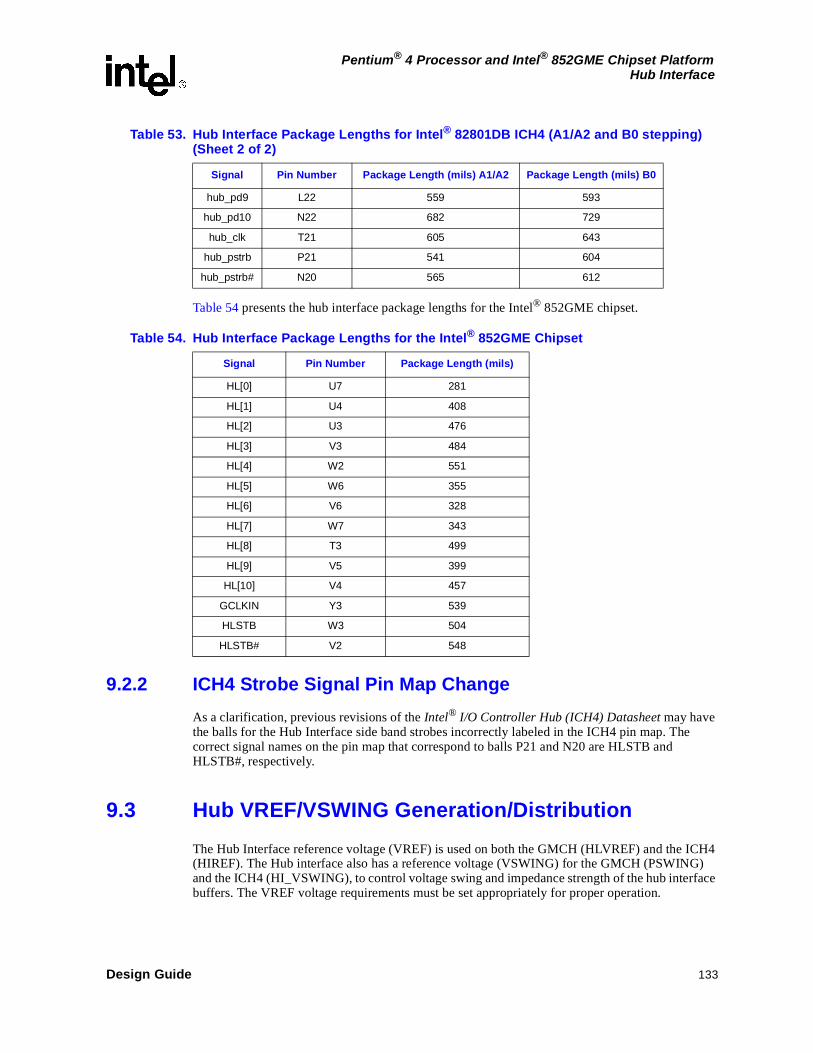
Design Guide 133
Pentium® 4 Processor and Intel® 852GME Chipset PlatformHub Interface
Table 54 presents the hub interface package lengths for the Intel® 852GME chipset.
9.2.2 ICH4 Strobe Signal Pin Map Change
As a clarification, previous revisions of the Intel® I/O Controller Hub (ICH4) Datasheet may have the balls for the Hub Interface side band strobes incorrectly labeled in the ICH4 pin map. The correct signal names on the pin map that correspond to balls P21 and N20 are HLSTB and HLSTB#, respectively.
9.3 Hub VREF/VSWING Generation/Distribution
The Hub Interface reference voltage (VREF) is used on both the GMCH (HLVREF) and the ICH4 (HIREF). The Hub interface also has a reference voltage (VSWING) for the GMCH (PSWING) and the ICH4 (HI_VSWING), to control voltage swing and impedance strength of the hub interface buffers. The VREF voltage requirements must be set appropriately for proper operation.
hub_pd9 L22 559 593
hub_pd10 N22 682 729
hub_clk T21 605 643
hub_pstrb P21 541 604
hub_pstrb# N20 565 612
Table 53. Hub Interface Package Lengths for Intel® 82801DB ICH4 (A1/A2 and B0 stepping) (Sheet 2 of 2)
Signal Pin Number Package Length (mils) A1/A2 Package Length (mils) B0
Table 54. Hub Interface Package Lengths for the Intel® 852GME Chipset
Signal Pin Number Package Length (mils)
HL[0] U7 281
HL[1] U4 408
HL[2] U3 476
HL[3] V3 484
HL[4] W2 551
HL[5] W6 355
HL[6] V6 328
HL[7] W7 343
HL[8] T3 499
HL[9] V5 399
HL[10] V4 457
GCLKIN Y3 539
HLSTB W3 504
HLSTB# V2 548

134 Design Guide
Pentium® 4 Processor and Intel® 852GME Chipset PlatformHub Interface
See Table 55 for the VREF and VSWING voltage specifications. Section 9.3.1 to Section 9.3.3 provide details on the different options for VREF and VSWING voltage divider circuitry requirements.
9.3.1 Single Generation Reference Voltage Divider Circuit
The GMCH and ICH4 may share the same single voltage divider circuit. This option provides one voltage divider circuit to generate both VREF and VSWING reference voltage. The reference voltage for both VREF and VSWING must meet the voltage specification in Table 55. When the voltage specifications are not met, an individual locally generated voltage divider circuit is required. The maximum trace length from the GMCH to ICH4 is 4 inches or less. Place the voltage divider circuit midway between the GMCH and ICH4. Normal care needs to be taken to minimize crosstalk to other signals (< 10-15 mV). When the trace length exceeds 4 inches, use the locally generated voltage reference divider.
Figure 54 shows the single VREF/VSWING voltage generation circuit for Hub Interface.
The resistor values R1, R2, and R3 must be rated at 1% tolerance. See Table 31 for recommended resistor value. The selected resistor values ensure that the reference voltage tolerance is maintained over the input leakage specification. Place two 0.1µF capacitors (C1 and C3) close to the divider. In addition, place the 0.01µF bypass capacitors (C2, C4, C5, and C6) within 0.25 inch of HLVREF/VREF pin (for C4 and C6) and HI_VSWING pin (for C2 and C5).
Table 56 presents the recommended resistor values for a single VREF/VSWING divider circuit.
Table 55. Hub Interface VREF/VSWING Generation Circuit Specifications
VREF VSWING
NotesHIREF (ICH4)
HLVREF (GMCH)HI_VSWING (ICH4) PSWING (GMCH)
350 mV ± 8% 800 mV ± 8%
See Sections 9.3.1, 9.3.2, and 9.3.3 for recommendations for the VREF/VSWING voltage generation circuitry.
See Table 31, Table 32, and Table 33 for recommended resistor values.
Figure 54. Single VREF/VSWING Voltage Generation Circuit for Hub Interface
B1360-01
C5
PVSWING
HLVREF
GMCHIntel®
82801DBICH4
C2C1 R2
R1
VCCHI = 1.2
R3C6 C4
C3
HI_VSWING
HIREF

Design Guide 135
Pentium® 4 Processor and Intel® 852GME Chipset PlatformHub Interface
9.3.2 Locally Generated Reference Voltage Divider Circuit
Section 9.3.2.1 and Section 9.3.2.2 provides the option to generate the voltage references separately for GMCH and ICH4. Use this option if the routing distance between GMCH and ICH4 is greater than 4 inches.
9.3.2.1 ICH4 Single Generated Voltage Reference Divider Circuit
This option allows the ICH4 to use one voltage divider circuit to generate both HIVREF and HI_VSWING voltage references. The reference voltage for both HIVREF and HI_VSWING must meet the voltage specification in Table 55. The resistor values R1, R2, and R3 must be rated at 1% tolerance (see Table 56). Normal care needs to be taken to minimize crosstalk to other signals (< 10-15 mV). When the voltage specifications are not met, individually generated voltage divider circuit for HIVREF and HI_VSWING are required.
Figure 55 shows an ICH4 locally generated voltage divider circuit.
Table 56. Recommended Resistor Values for A Single VREF/VSWING Divider Circuit
Option Recommended Resistor Values VCCHI
Option 1 R1 = 80.6 Ω ± 1% R2 = 51.1 Ω ± 1% R3 = 40.2 Ω ± 1% 1.5 V
Option 2 R1 = 255 Ω ± 1% R2 = 162 Ω ± 1% R3 = 127 Ω ± 1% 1.5 V
Option 3 R1 = 226 Ω ± 1% R2 = 147 Ω ± 1% R3 = 113 Ω ± 1% 1.5 V
C1 and C3 = 0.1µF (near divider)
C2, C4, C5, and C6 = 0.01µF (near component)
Figure 55. Intel® 82801DB ICH4 Locally Generated Reference Voltage Divider Circuit
B1361-01
Intel®
82801DBICH4
C2R2
R1
VCCHI
R3C4
C1
C3
HI_VSWING
HIREF

136 Design Guide
Pentium® 4 Processor and Intel® 852GME Chipset PlatformHub Interface
9.3.2.2 GMCH Single Generated Voltage Reference Divider Circuit
This option allows the GMCH to use one voltage divider circuit to generate both HLVREF and HLPSWING voltage references. The reference voltage for both HLVREF and HLPSWING must meet the voltage specification in Table 55. The resistor values R1, R2, and R3 must be rated at 1% tolerance (see Table 56). Normal care needs to be taken to minimize crosstalk to other signals (< 10-15 mV). When the voltage specifications are not met, individually generated voltage divider circuits for HLVREF and PSWING are required. Figure 56 shows the GMCH locally generated reference voltage divider circuit.
Figure 56. GMCH Locally Generated Reference Voltage Divider Circuit
B1362-01
GMCHC5C1
R2
R1
VCCHI
R3C6C3
PSWING
HLVREF

Design Guide 137
Pentium® 4 Processor and Intel® 852GME Chipset PlatformHub Interface
9.3.3 Separate GMCH and ICH4 Voltage Divider Circuits for VREF and VSWING
Section 9.3.3.1 and Section 9.3.3.2 provides the option to generate individual voltage reference for VREF and VSWING separately for GMCH and ICH4.
9.3.3.1 Separate ICH4 Voltage Divider Circuits for HIVREF and HI_VSWING
This option allows for tuning the voltage references HIVREF and HI_VSWING individually. The reference voltage for both HIVREF and HI_VSWING must meet the voltage specification in Table 55. Normal care needs to be taken to minimize crosstalk to other signals (< 10-15 mV). Figure 57 shows individual HIVREF and HI_VSWING voltage reference divider circuits for the ICH4.
Table 57 presents the recommended resistor values for HIVREF and HIVSWING divider circuits for the ICH4.
Figure 57. Individual HIVREF and HI_VSWING Voltage Reference Divider Circuitsfor the Intel® 82801DB ICH4
B1363-01
C1
R4 R6
VCCHI
R5 R7
C4 C3
C2Intel®
82801DBICH4
HI_VSWING
HIVREF
Table 57. Recommended Resistor Values for HIVREF and HI_VSWING Divider Circuitsfor the Intel® 82801DB ICH4
Signal Recommended Resistor Values VCCHI Capacitor value
HIVREF (350 mV)
R4 = 487 Ω ± 1%
R5 = 150 Ω ± 1%VCCHI = 1.5 V
C3 = 0.1µF (near divider)
C2 = 0.01µF (near component)
HI_VSWING (800 mV)
R6 = 130 Ω ± 1%
R7 = 150 Ω ± 1%VCCHI = 1.5 V
C1 = 0.1µF (near divider)
C4 = 0.01µF (near component)

138 Design Guide
Pentium® 4 Processor and Intel® 852GME Chipset PlatformHub Interface
9.3.3.2 Separate GMCH Voltage Divider Circuits for HLVREF and PSWING
This option allows for tuning the voltage references HLVREF and PSWING individually. The reference voltage for both HLVREF and PSWING must meet the voltage specification in Table 55. Normal care needs to be taken to minimize crosstalk to other signals (< 10-15 mV).
Figure 58 shows the individual HLVREF and PSWING voltage reference divider circuits for GMCH.
Table 58 presents the recommended resistor values for HLVREF and PSWING divider circuits for GMCH.
9.4 Hub Interface Decoupling Guidelines
To improve I/O power delivery, use two 0.1µF capacitors for each component (that is, the ICH4 and GMCH). Place these capacitors within 50 mils from each package, adjacent to the rows that contain the Hub Interface. When the layout allows, wide metal fingers running on the VSS side of the board should connect the VCCHI side of the capacitors to the VCCHI power pins. Similarly, when layout allows, metal fingers running on the VCCHI side of the board should connect the ground side of the capacitors to the VSS power pins.
Figure 58. Individual HLVREF and PSWING Voltage Reference Divider Circuits for GMCH
B1364-01
C1
R4 R6
VCCHI
R5 R7
C5 C3
C6GMCH
PSWING
HLVREF
Table 58. Recommended Resistor Values for HLVREF and PSWING Divider Circuits for GMCH
Signal Name Recommended Resistor Values VCCHI Capacitor
HLVREF (350 mV)
R4 = 324 Ω ± 1%
R5 = 100 Ω ± 1%VCCHI = 1.5 V
C3 = 0.1µF (near divider);
C6 = 0.01µF (near component)
PSWING (800 mV)
R6 = 86.6 Ω ± 1%
R7 = 100 Ω ± 1%VCCHI = 1.5 V
C1 = 0.1µF (near divider)
C5 = 0.01µF (near component)

Design Guide 139
Pentium® 4 Processor and Intel® 852GME Chipset PlatformAGP Port Design Guidelines
AGP Port Design Guidelines 10
For detailed AGP interface functionality (for example, protocols, rules, signaling mechanisms), refer to the latest AGP Interface Specification, Revision 2.0, which may be obtained athttp://www.agpforum.org
10.1 AGP Interface
The AGP Interface Specification, Revision 2.0, enhances the functionality of the original AGP Interface Specification (Revision 1.0) by allowing 4X data transfers (four data samples per clock) and 1.5 V operation. This functionality is not 3.3 V safe. In addition to these major enhancements, additional performance enhancement and clarifications, such as fast write capability, are included in Revision 2.0 of the AGP Interface Specification.
The 4X operation of the AGP interface provides for quad-sampling of the AGP AD (Address/Data) and SBA (Side-band Addressing) buses. That is, the data is sampled four times during each 66 MHz AGP clock. This means that each data cycle is ¼ of a 15 ns period (66 MHz clock) or 3.75 ns. It is important to realize that 3.75 ns is the data cycle time, not the clock cycle time. During 2X operation, the data is sampled twice during a 66 MHz clock cycle. Therefore, the data cycle time is 7.5 ns.
To allow for these high-speed data transfers, the 2X mode of AGP operation uses source synchronous data strobing. During 4X operation, the AGP interface uses differential source synchronous data strobing. However, differential source synchronous data strobing is not strictly required by the AGP specification.
With data cycle times as small as 3.75 ns, and setup/hold times of 1 ns, propagation delay mismatch is critical. In addition to reducing propagation delay mismatch, it is important to minimize noise. Noise on the data lines cause the settling time to be large. When the mismatch between a data line and the associated strobe is too great, or there is noise on the interface, incorrect data will be sampled.
The low-voltage operation on AGP (1.5 V) requires even more noise immunity. For example, during 1.5 V operation, Vilmax is 570 mV. Without proper isolation, crosstalk could create signal integrity issues.
A single AGP controller is supported by the GMCH AGP interface. LOCK# and SERR#/PERR# are not supported. The AGP buffers operate in one mode: AGP 4X, 2X and 1X operate only at1.5 V.
AGP semantic cycles to DRAM are not snooped on the host bus.
The GMCH supports PIPE# or SBA[7:0] AGP address mechanisms, but not both simultaneously. Either the PIPE# or the SBA[7:0] mechanism must be selected during system initialization.
The AGP interface is clocked from the 66 MHz clock input to the MCH, 66IN. The AGP interface is synchronous to the host and system memory interfaces with a clock ratio of 2:3 (66 MHz: 100 MHz) and to the hub interface with a clock ratio of 1:1 (66 MHz: 66 MHz).
Note: AGP features is not supported when ECC is turned on

140 Design Guide
Pentium® 4 Processor and Intel® 852GME Chipset PlatformAGP Port Design Guidelines
10.2 AGP 2.0 Specification
10.2.1 AGP 2.0
The AGP Interface Specification, Revision 2.0, enhances the functionality of the original AGP Interface Specification, Revision 1.0, by allowing 4X data transfers (i.e., four data samples per clock), and 1.5 V operation. The 4X operation of the AGP interface provides for quad-pumping of the AGP AD (address/data) and SBA (side-band addressing) buses. That is, data is sampled four times during each 66 MHz AGP clock. This means that each data cycle is ¼ of a 15-ns (66 MHz) clock or 3.75 ns. It is important to understand that 3.75 ns is the data cycle time, not the clock cycle time. During 2X operation, data is sampled twice during a 66 MHz clock cycle.
Therefore, the data cycle time is 7.5 ns. To allow for these high-speed data transfers, the 2X mode of AGP operation uses source-synchronous data strobing. During 4X operation, the AGP interface uses differential source-synchronous strobing.
With data cycle times as small as 3.75 ns and setup/hold times of 1 ns, propagation delay mismatch is critical. In addition to reducing propagation delay mismatch, it is important to minimize noise. Noise on the data lines will cause the settling time to be long. If the mismatch between a data line and the associated strobe is too great, or if there is noise on the interface, incorrect data will be sampled. The low-voltage operation on AGP (1.5 V) requires even more noise immunity.
10.2.2 AGP Interface Signal Groups
The signals on the AGP interface are broken into three groups: 1X timing domain signals, 2X/4X timing domain signals, and miscellaneous signals. Each group has different routing requirements. In addition, within the 2X/4X timing domain signals, there are three sets of signals. All signals in the 2X/4X timing domain must meet minimum and maximum trace length requirements as well as trace width and spacing requirements. Table 59 presents the AGP 2.0 signal groups.
Table 59. AGP 2.0 Signal Groups (Sheet 1 of 2)
Timing Domain Signals
1X timing domain
CLK (3.3 V)
RBF#
WBF#
ST[2:0]
PIPE#
REQ#
GNT#
PAR
FRAME#
IRDY#
TRDY#
STOP#
DEVSEL#
† These signals are used in 2X & 4X AGP mode ONLY.

Design Guide 141
Pentium® 4 Processor and Intel® 852GME Chipset PlatformAGP Port Design Guidelines
Table 60 presents the AGP 2.0 data/strobe associations.
Throughout this section, the term data refers to AD[31:0], C/BE[3:0]#, and SBA[7:0]. The term strobe refers to AD_STB[1:0], AD_STB#[1:0], SB_STB, and SB_STB#. When the term data is used, it refers to one of the three sets of data signals, as in Table 60. When the term strobe is used, it refers to one of the strobes as it relates to the data in its associated group.
The routing guidelines for each group of signals (1X timing domain signals, 2X/4X timing domain signals, and miscellaneous signals) are addressed separately.
2X / 4X timing domain
Set #1
AD[15:0]
C/BE[1:0]#
AD_STB0
AD_STB0#†
Set #2
AD[31:16]
C/BE[3:2]#
AD_STB1
AD_STB1#†
Set #3
SBA[7:0]
SB_STB
SB_STB#†
Miscellaneous, Asynchronous
USB+
USB-
OVRCNT#
PME#
TYPDET#
PERR#
SERR#
INTA#
INTB#
Table 59. AGP 2.0 Signal Groups (Sheet 2 of 2)
Timing Domain Signals
† These signals are used in 2X & 4X AGP mode ONLY.
Table 60. AGP 2.0 Data/Strobe Associations
Data Associated Strobe in 1X Associated Strobe in 2X
Associated Strobes in 4X
AD[15:0] and C/BE[1:0]#Strobes are not used in 1X mode. All data is sampled on rising clock edges.
AD_STB0 AD_STB0, AD_STB0#
AD[31:16] and C/BE[3:2]#Strobes are not used in 1X mode. All data is sampled on rising clock edges.
AD_STB1 AD_STB1, AD_STB1#
SBA[7:0]Strobes are not used in 1X mode. All data is sampled on rising clock edges.
SB_STB SB_STB, SB_STB#

142 Design Guide
Pentium® 4 Processor and Intel® 852GME Chipset PlatformAGP Port Design Guidelines
10.3 AGP Routing Guidelines
10.3.1 1x Timing Domain Routing Guidelines
10.3.1.1 Trace Length Requirements for AGP 1X
This section contains information on the 1X timing domain routing guidelines. The AGP 1X timing domain signals (refer to Table 61) have a maximum trace length of 10 inches. The target impedance is 55 Ω ± 15%. This maximum applies to ALL of the signals listed as 1X timing domain signals in Table 61. In addition to this maximum trace length requirement (refer to Table 61 and Table 62), these signals must meet the trace spacing and trace length mismatch requirements in Section 10.3.1.2 and Section 10.3.1.3.
Table 61 presents the layout routing guidelines for AGP 1X signals.
10.3.1.2 Trace Spacing Requirements
AGP 1X timing domain signals (refer to Table 61) may be routed with 4 mils of minimum trace separation.
10.3.1.3 Trace Length Mismatch
There are no trace length mismatch requirements for 1X timing domain signals. These signals must meet minimum and maximum trace length requirements.
Table 61. Layout Routing Guidelines for AGP 1X Signals
1X Signals Max. Length (inches) Width (mils) Space (mils)
CLK_AGP_SLT 10 4 4
AGP_PIPE# 10 4 4
AGP_RBF# 10 4 4
AGP_WBF# 10 4 4
AGP_ST[2:0] 10 4 4
AGP_FRAME# 10 4 4
AGP_IRDY# 10 4 4
AGP_TRDY# 10 4 4
AGP_STOP# 10 4 4
AGP_DEVSEL# 10 4 4
AGP_REQ# 10 4 4
AGP_GNT# 10 4 4
AGP_PAR 10 4 4

Design Guide 143
Pentium® 4 Processor and Intel® 852GME Chipset PlatformAGP Port Design Guidelines
10.3.2 2x/4x Timing Domain Routing Guidelines
10.3.2.1 Trace Length Requirements for AGP 2X/4X
These trace length guidelines apply to ALL of the signals listed as 2X/4X timing domain signals in Table 62. In addition to these maximum trace length requirements, these signals must meet the trace spacing and trace length mismatch requirements in Section 10.3.2.2 and Section 10.3.2.3.
The maximum line length and mismatch requirements are dependent on the routing rules used on the motherboard. These routing rules were created to give design freedom by making tradeoffs between signal coupling (trace spacing) and line lengths. These routing rules are divided by trace spacing. In 1:2 spacing, the distance between the traces is two times the width of traces. Simulations in a mobile environment support this rule.
Figure 59 shows the AGP layout guidelines.
When the AGP interface is less than 6.0 inches, 1:2 trace spacing is required for 2X/4X lines. These 2X/4X signals must be matched to their associated strobe within ± 0.1 inch. This is for designs that require less than six inches between the graphics device and the MCH. Reduce line length mismatch to ensure added margin. In order to reduce trace to trace coupling (cross talk), separate the traces as much as possible.
10.3.2.2 Trace Spacing Requirements
AGP 2X/4X timing domain signals must be routed as documented in Table 62. Route the signals using 4 mil traces. Additionally, the signals may be routed with 5 mil spacing when breaking out of the MCH. The routing must widen to the requirement in Table 63 within 0.3 inch of the MCH package.
Since the strobe signals (AD_STB0, AD_STB0#, AD_STB1, AD_STB1#, SB_STB, and SB_STB#) act as clocks on the source synchronous AGP interface, take special care when routing these signals. Because each strobe pair is truly a differential pair, route the pair together (for example, route AD_STB0 and AD_STB0# next to each other). Route the two strobes in a strobe pair on 4 mil traces with 8 mils of space (1:2) between them. Separate this pair from the rest of the AGP signals (and all other signals) by at least 15 mils (1:3). The strobe pair must be length matched to less than ± 0.1 inch (that is, a strobe and its compliment must be the same length within ± 0.1 inch). Table 62 presents the layout routing guidelines for AGP 2X/4X signals.
Figure 59. AGP Layout Guidelines
B 1 4 1 3 -0 1
G M C HA G P
C o n tro lle r
L in e :S p a c eA lw a ys 1 :2 S tro b e to S tro b e # R o u t in gA lw a ys 1 :3 S tro b e to S tro b e # D a ta R o u t in g
1 :2 R o u t in g6 .0 in c h e s m a x im u m le n g th± 0 .1 in c h m is m a tc h

144 Design Guide
Pentium® 4 Processor and Intel® 852GME Chipset PlatformAGP Port Design Guidelines
10.3.2.3 Trace Length Mismatch Requirements
Table 63 presents the AGP 2.0 data lengths relative to strobe length.
Apply the trace length minimum and maximum (relative to strobe length) to each set of 2X/4X timing domain signals independently. That is, if AD_STB0 and ADSTB0# are five inches, then AD[15:0] and C/BE[1:0] must be between 4.9 inches and 5.1 inches. However, AD_STB1 and ADSTB1# may be 3.5 inches (and therefore AD[31:16] and C/BE#[3:2] must be between 3.4 inches and 3.6 inches). In addition, all 2X/4X timing domain signals must meet the maximum trace length requirements.
• Route all signals as strip lines (inner layers).
• Route all signals in a signal group on the same layer. Routing studies have shown that these guidelines may be met. The trace length and trace spacing requirements must not be violated by any signal. Verify that the trace length mismatch for all signals within a signal group is as close to 0 inches as possible to provide optimal timing margin.
The strobe pair must be length matched to less than +/- 0.01 inches (that is, a strobe and its compliment must be the same length within +/- 0.01 inches)
Table 64 presents the AGP 2.0 routing summary.
Table 62. Layout Routing Guidelines for AGP 2X/4X Signals
SignalMaximum
Length (inch)
Trace Space (mils)
(4 mil traces)
Length Mismatch
(inch)Relative To Notes
2X/4X Timing Domain Set#1 6 8 ± 0.1
AGP_ADSTB0 and AGP_ADSTB0#
AGP_ADSTB0, AGP_ADSTB0# must be the same length (± 10 mils)
2X/4X Timing Domain Set#2 6 8 ± 0.1
AGP_ADSTB1 and AGP_ADSTB1#
AGP_ADSTB1, AGP_ADSTB1# must be the same length (± 10 mils)
2X/4X Timing Domain Set#3 6 8 ± 0.1 AGP_SBSTB and
AGP_SBSTB #
AGP_SBSTB, AGP_SBSTB# must be the same length (± 10 mils)
Table 63. AGP 2.0 Data Lengths Relative to Strobe Length
Max Trace Length Trace Spacing Strobe Length Min Trace Length Max Trace Length
< 6 in 1:2 X X – 0.1 in X + 0.1 in
Table 64. AGP 2.0 Routing Guideline Summary (Sheet 1 of 2)
Signal Maximum Length
Trace Spacing(4 mil traces)
Length Mismatch Relative To Notes
1X Timing Domain 10 in 4 mils No Requirement N/A None
2X/4X Timing Domain Set#1 6 in 8 mils ± 0.1 in
AD_STB0 and AD_STB0#
AD_STB0, AD_STB0# must be the same length

Design Guide 145
Pentium® 4 Processor and Intel® 852GME Chipset PlatformAGP Port Design Guidelines
Each strobe pair must be separated from other signals by at least 15 mils.
10.3.3 AGP Clock Skew
The maximum total AGP clock skew, between the GMCH and the graphics component, is 1 ns for all data transfer modes. This 1 ns includes skew and jitter that originates on the motherboard, add-in module (if used), and clock synthesizer. Clock skew must be evaluated not only at a single threshold voltage, but also at all points on the clock edge that falls in the switching range. The 1 ns skew budget is divided such that the motherboard is allotted 0.9 ns of clock skew (the motherboard designer should determine how the 0.9 ns is allocated between the board and the synthesizer).
10.3.4 AGP Signal Noise Decoupling Guidelines
The following decoupling guidelines are preliminary and subject to change in future revisions of this document. The main focus of these guidelines is to minimize signal integrity problems on the AGP interface of the Intel chipset GMCH. The following guidelines are not intended to replace thorough system validation on Intel chipset-based products.
• A minimum of six 0.01 µF capacitors are required and must be as close as possible to the MCH. Place these capacitors within 70 mils of the outer row of balls on the MCH for VDDQ decoupling. Ideally, this should be as close as possible.
• Evenly distribute placement of decoupling capacitors in the AGP interface signal field.
• Intel recommends that the designer use a low-ESL ceramic capacitor, such as with a 0603 body-type X7R dielectric.
• In order to add the decoupling capacitors within 70 mils of the MCH and/or close to the vias, the trace spacing may be reduced as the traces go around each capacitor. The narrowing of space between traces should be minimal and for as short a distance as possible (1.0 inch max.).
In addition to the minimum decoupling capacitors, the designer should place bypass capacitors at vias that transition the AGP signal from one reference signal plane to another. One extra 0.01 µF capacitor per 10 vias is required. Place the capacitor as close as possible to the center of the via field.
2X/4X Timing Domain Set#2 6 in 8 mils ± 0.1 in
AD_STB1 and AD_STB1#
AD_STB1, AD_STB1# must be the same length
2X/4X Timing Domain Set#3 6 in 8 mils ± 0.1 in SB_STB and
SB_STB#
SB_STB, SB_STB# must be the same length
Miscellaneous 10 in 8 mils No Requirement N/APCI_PME#, AGP_PERR#, AGP_SERR#
Table 64. AGP 2.0 Routing Guideline Summary (Sheet 2 of 2)
Signal Maximum Length
Trace Spacing(4 mil traces)
Length Mismatch Relative To Notes

146 Design Guide
Pentium® 4 Processor and Intel® 852GME Chipset PlatformAGP Port Design Guidelines
10.3.5 AGP Interface Package Lengths
Table 65 presents the ABP interface package lengths.
Table 65. AGP Interface Package Lengths (Sheet 1 of 2)
Signal Pin Number Package Length (mils)
GAD0 T6 339
GAD1 T5 362
GAD2 R5 440
GAD3 R3 489
GAD4 R4 415
GAD5 R6 343
GAD6 P5 387
GAD7 P6 409
GAD8 N5 466
GAD9 N3 504
GAD10 N2 568
GAD11 M5 510
GAD12 M1 611
GAD13 M3 520
GAD14 M2 566
GAD15 T7 296
GAD16 L5 440
GAD17 K6 491
GAD18 L3 541
GAD19 K5 489
GAD20 K1 692
GAD21 K3 622
GAD22 K2 685
GAD23 J6 536
GAD24 H1 772
GAD25 H2 720
GAD26 H4 625
GAD27 H3 649
GAD28 G3 762
GAD29 H6 521
GAD30 G2 712
GAD31 H5 566
GADSTB_0 P3 475
GADSTBB_0 P4 439

Design Guide 147
Pentium® 4 Processor and Intel® 852GME Chipset PlatformAGP Port Design Guidelines
10.3.6 AGP Routing Ground Reference
Intel recommends that at least the following critical signals be referenced to ground from the MCH to an AGP controller connector using a minimum number of vias on each net: AD_STB0, AD_STB0#, AD_STB1, AD_STB1#, SB_STB, SB_STB#, G_TRDY#, G_IRDY#, G_GNT#, and ST[2:0].
GADSTB_1 J3 601
GADSTBB_1 J2 675
GSBA_0 E5 686
GSBA_1 F5 617
GSBA_2 E3 738
GSBA_3 E2 865
GSBA_4 G5 668
GSBA_5 F4 688
GSBA_6 G6 518
GSBA_7 F6 613
GSBSTB F2 799
GSBSTBB F3 761
GPIPEB D5 644
GCBEB_0 P2 553
GCBEB_1 L2 583
GCBEB_2 L4 515
GCBEB_3 J5 518
GST_0 C4 750
GST_1 C3 797
GST_2 C2 856
GRBFB D3 962
GWBFB D2 947
GFRAMEB M6 486
GIRDYB K7 751
GTRDYB N7 350
GSTOPB P7 423
GDEVSELB N6 399
GREQB B3 762
GGNTB B2 849
GPAR L7 623
Table 65. AGP Interface Package Lengths (Sheet 2 of 2)
Signal Pin Number Package Length (mils)

148 Design Guide
Pentium® 4 Processor and Intel® 852GME Chipset PlatformAGP Port Design Guidelines
In addition to the minimum signal set listed previously, Intel recommends that half of all AGP signals be referenced to ground, depending on the board layout. In an ideal design, the complete AGP interface signal field would be referenced to ground. This recommendation is not specific to any particular PCB stack-up, but should be applied to all Intel chipset designs.
10.3.7 Pull-Ups
The AGP 2.0 Specification requires AGP control signals to have pull-up resistors to VDDQ to ensure they contain stable values when no agent is actively driving the bus. Also, the AD_STB[1:0]# and ST_STB# strobes require pull-down resistors to ground. The Intel® 855PM chipset MCH has integrated many of these pull-up/pull-down resistors on the AGP interface and a few other signals not required by the AGP 2.0 Specification. Pull-ups are allowed on any signal except AD_STB[1:0]# and ST_STB#.
The Intel chipset GMCH has no support for the PERR# and SERR# pins of an AGP graphics controller that supports PERR# and SERR#. Pull-ups to a 1.5 V source are required down on the motherboard in such cases.

Design Guide 149
Pentium® 4 Processor and Intel® 852GME Chipset PlatformAGP Port Design Guidelines
Table 66 presents the AGP pull-up/pull-down requirements and straps.
Table 67 presents the AGP 2.0 pull-up/pull-down resistor value requirements.
The recommended AGP pull-up/pull-down resistor value is 8.2 kΩ.
Table 66. AGP Pull-Up/Pull-Down Requirements and Straps
Signal AGP 2.0 Signal Pull-up/Pull down Requirements
MCH Integrated Pull-Up/Pull-Down
State During RSTIN# Assertion Notes
DEVSEL# Pull-Up
FRAME# Pull-Up
GNT# Pull-Up Pull-Up (Strap) 5
INTA# Pull-Up 3, 4
INTB# Pull-Up 3, 4
IRDY# Pull-Up
PERR# Pull-Up 2
PIPE# Pull-Up
RBF# Pull-Up Pull-Up (Strap) 5
REQ# Pull-Up 1
SERR# Pull-Up 2
ST[2:0] Pull-Down Pull-Up (Strap) 5
STOP# Pull-Up Pull-Up
TRDY# Pull-Up
WBF# Pull-Up Pull-Up (Strap) 5
AD_STB[1:0] Pull-Up
AD_STB[1:0]# Pull-Down
SB_STB Pull-Up
SB_STB# Pull-Down
SBA[7:0] Pull-Up Pull-Up (Strap) 1, 5
NOTES:1. The Intel chipset GMCH has integrated pull-ups to ensure that these signal do not float when there is no
add-in card in the connector.2. The Intel chipset MCH does not implement the PERR# and SERR# signals. Pull-ups on the motherboard
are required for AGP graphics controllers that implement these signals.3. The Intel chipset MCH does not implement interrupt signals. The AGP graphics controller’s INTA# and
INTB# signals must but routed to the system PCI interrupt request handler where the pull-up requirement should be met as well. For Intel® 852GME chipset / Intel® 82801DB ICH4 chipset-based systems, they may be routed to the ICH4’s PIRQ signals that are open drain and require pull-ups on the motherboard.
4. INTA# and INTB# should be pulled to 3.3 V, not VDDQ.5. Refer to the Intel(R) 852GME and Intel(R) 852PM Chipset MCH Datasheet for more details on straps.
Table 67. AGP 2.0 Pull-up/Pull-down Resistor Values
Rmin Rmax
4 kΩ 16 kΩ

150 Design Guide
Pentium® 4 Processor and Intel® 852GME Chipset PlatformAGP Port Design Guidelines
10.3.8 AGP VDDQ and VREF
AGP specifies two separate power planes: VCC and VDDQ. VCC is the core power for the graphics controller. VDDQ is the interface voltage. The external graphics controller may ONLY power the MCH AGP I/O buffers with 1.5 V, VDDQ power pins.
10.3.9 VREF Generation for AGP 2.0 (2X and 4X)
10.3.9.1 1.5 Volt AGP Interface (2X/4X)
To account for potential differences between VDDQ and ground at the MCH and graphics controller, both devices use source generated Vref. That is, the Vref signal is generated at the graphics controller and sent to the MCH and another Vref is generated at the MCH and sent to the graphics controller.
Both the graphics controller and the MCH are required to generate Vref. The voltage divider networks consist of AC and DC elements. The reference voltage that should be supplied to the Vref pins of the MCH and the graphics controller is ½ * VDDQ. Two, 1 kΩ ± 1% resistors may be used to divide VDDQ down to the necessary voltage level.
Place the Vref divider network as close to the AGP interface as is practical to get the benefit of the common mode power supply effects. However, the trace spacing around the Vref signals must be a minimum of 25 mils to reduce crosstalk and maintain signal integrity.
10.3.10 AGP Compensation
The Intel® 852GME chipset MCH AGP interface supports resistive buffer compensation. For printed circuit boards with characteristics impedance of 55 Ω, tie the GRCOMP pin to a 36.5 Ω ± 1% pull-down resistor (to ground) through a 10 mil wide, very short (≈ 0.5 inch) trace.
10.3.11 AGP Reference Information
Information about APG technology may be obtained at:
http://www.intel.com/technology/agp/info.htm.
Information about the APG stress tool may be obtained at:
http://www.intel.com/technology/agp/downloads/agp_stress.htm
.

Design Guide 151
Pentium® 4 Processor and Intel® 852GME Chipset PlatformI/O Subsystem
I/O Subsystem 11
11.1 SYS_RESET# Usage Model
The System Reset signal (SYS_RESET#) on the Intel® 82801DB ICH4 (ICH4) may be connected directly to the reset button on the system’s front panel, provided that the front panel header pulls this signal up to 3.3 V standby through a weak pull-up resistor. The ICH4 has internal logic to debounce this signal for 16 ms, allowing the SMBus to go idle before resetting the system. This helps prevent slave devices on the SMBus from hanging because they are reset in the middle of a cycle.
When a Pentium® 4 processor ITP700FLEX debug port is implemented on the system, Intel recommends that the DBR# signal of the ITP interface be connected to SYS_RESET# as well.
11.2 PWRBTN# Usage Model
The Power Button signal (PWRBTN#) on the ICH4 may be connected directly to the power button on the system’s front panel. This signal is internally pulled-up to 3.3 V standby through a weak pull-up resistor (24 kΩ nominal). The ICH4 has internal logic to debounce this signal for 16 ms. Figure 60 shows the SYS_RESET# and PWRBTN# connection.
Figure 60. SYS_RESET# and PWRBTN# Connection
Note:SYS_RESET# is 3.3 V tolerant. Pull this signalup to 3.3 V standby by the front panel header.
MCH
RSTIN#
FWH
SIO
RST
PCI_RESET
PCIRST#
SYS_RESET#
PWRBTN#
PWROK
Intel®
82801DBICH4
FrontPanel
Header
LevelShifter
ATXPowerSupply
PWRGD_PS
B1374-01

152 Design Guide
Pentium® 4 Processor and Intel® 852GME Chipset PlatformI/O Subsystem
11.3 Power Well Isolation Control Strap Requirements
The circuit shown in Figure 61 may be implemented to control well isolation between the VCCSUS3_3 and RTC power wells in the event that RSMRST# is not being actively asserted during the discharge of the standby rail. Failure to implement this circuit or a circuit that functions similar to this may result in excessive droop on the VCCRTC node during Sx-to-G3 power state transitions (removal of AC power and battery power). Droop on this node may potentially cause the CMOS to be cleared or corrupted, the RTC to lose time after several AC/battery power cycles, or the intruder bit might assert erroneously.
11.4 IDE Interface
This section contains guidelines for connecting and routing the ICH4 IDE interface. The ICH4 has two independent IDE channels. The ICH4 has integrated the series resistors that have been typically required on the IDE data signals (PDD[15:0] and SDD[15:0]) running to the two ATA connectors. While it is not anticipated that additional series termination resistors will be required, OEMs need to verify motherboard signal integrity through simulation. Additional external 0 Ω resistors may be incorporated into the design to address possible noise issues on the motherboard. The additional resistor layout increases flexibility by offering stuffing options at a later date.
The IDE interface may be routed with 5 mil traces on 7 mil spaces, and must be less than eight inches long (from ICH4 to IDE connector). Additionally, the maximum length difference between the shortest data signal and the longest strobe signal of a channel is 0.5 inch.
Figure 61. RTC Power Well Isolation Control
BAV99
BAV99
2.2 KΩ
No Stuff
No Stuff
MMBT3906
10 KΩ
RSMRST#
Intel®
82801DBICH4
RSMRST#generation
from MB logic
B1375-01

Design Guide 153
Pentium® 4 Processor and Intel® 852GME Chipset PlatformI/O Subsystem
11.4.1 Cabling
• Length of cable: Each IDE cable must be equal to or less than 18 inches.
• Capacitance: Less than 35 pF
• Placement: A maximum of six inches between drive connectors on the cable. When a single drive is placed on the cable, place the drive at the end of the cable. When a second drive is placed on the same cable, place the drive on the next closest connector to the end of the cable (six inches away from the end of the cable).
• Grounding: Provide a direct low impedance chassis path between the motherboard ground and hard disk drives.
• ICH4 Placement: The ICH4 must be placed equal to or less than eight inches from the ATA connector(s).
11.4.1.1 Cable Detection for Ultra ATA 66 and Ultra ATA100
The ICH4 IDE Controller supports PIO, Multi-word (8237 style) DMA, Ultra DMA modes 0 through 5, and Native Mode IDE.
Note: There are no motherboard hardware requirements for supporting Native Mode IDE. Native Mode IDE is supported through the operating system and system drivers. The ICH4 must determine the type of cable that is present to configure itself for the fastest possible transfer mode that the hardware may support.
An 80-conductor IDE cable is required for Ultra DMA modes greater than two (Ultra ATA/33). This cable uses the same 40-pin connector as the old 40-pin IDE cable. The wires in the cable alternate: ground, signal, ground, signal, ground, signal, ground, etc. All the ground wires are tied together on the cable (and they are tied to the ground on the motherboard through the ground pins in the 40-pin connector). This able conforms to the Small Form Factor Specification SFF-8049. This specification may be obtained from the Small Form Factor Committee.
To determine if Ultra DMA modes greater than two (Ultra ATA/33) may be enabled, the ICH4 requires the system software to determine the cable type used in the system. When the system software detects an 80-conductor cable, it may use any Ultra DMA mode up to the highest transfer mode supported by both the chipset and the IDE device. When a 40-conductor cable is detected, the system software must not enable modes faster than Ultra DMA Mode 2 (Ultra ATA/33).
Intel recommends that cable detection be performed using a combination Host-Side/Device-Side detection mechanism.
Note: Host-side detection cannot be implemented on an NLX form factor system because this configuration does not define interconnect pins for the PDIAG#/CBLID# from the riser (containing the ATA connectors) to the motherboard. These systems must rely solely on the device-side detection mechanism.

154 Design Guide
Pentium® 4 Processor and Intel® 852GME Chipset PlatformI/O Subsystem
11.4.1.2 Combination Host Side/Device Side Cable Detection
Host side detection (described in the ATA/ATAPI-6 Standard) requires the use of two GPI pins (one for each IDE channel). The proper way to connect the PDIAG#/CBLID# signal of the IDE connector to the host is shown in Figure 62. All IDE devices have a 10 kΩ pull-up resistor to 5 V on this signal. A 10 kΩ pull-down resistor on PDIAG#/CBLID# is required to prevent the GPIO from floating if a device is not present, and allows for use of a non 5 V tolerant GPIO.
This mechanism allows the BIOS, after diagnostics, to sample PDIAG#/CBLID#. When the signal is high, there is 40-conductor cable in the system, and Ultra DMA modes greater than two must not be enabled.
When PDIAG#/CBLID# is detected low, there may be an 80-conductor cable in the system, or there may be a 40-conductor cable and a legacy slave device (Device 1) that does not release the PDIAG#/CBLID# signal as required by the ATA/ATAPI-6 Standard. In this case, BIOS should check the IDENTIFY DEVICE information in a connected device that supports Ultra DMA modes higher than 2. When ID Word 93, bit 13, is set to one, an 80-conductor cable is present. When this bit is set to zero, a legacy slave (Device 1) is preventing proper cable detection, and BIOS should configure the system as though a 40-conductor cable is present and should notify the user of the problem.
Figure 62. Combination Host-Side/Device-Side IDE Cable Detection
80-conductor
IDE cable
IDE drive
5 V
GPIO
GPIO
Open
IDE drive
5 V
40-conductorcable
IDE drive
5 V
PDIAG#
Intel®
82801DBICH4
GPIO
GPIO
IDE drive
5 V
PDIAG#
PDIAG#PDIAG#
10 kΩ
10 k Ω
To secondaryIDE connector
PDIAG#/CBLID#
PDIAG#/CBLID#
10 kΩ
10 kΩ
10 kΩ
10 kΩ
B1376-01
Resistor required f ornon 5V tolerant GPI
To secondaryIDE connector
Resistor required f ornon 5 V tolerant GPI
Intel®
82801DBICH4

Design Guide 155
Pentium® 4 Processor and Intel® 852GME Chipset PlatformI/O Subsystem
11.4.1.3 Device Side Cable Detection
For platforms that must implement device-side detection only (for example, NLX platforms), a 0.047 µF capacitor is required on the motherboard as shown in Figure 63. This capacitor should not be populated when implementing the recommended combination host-side/device-side cable detection mechanism described above.
Note: Some drives may not support device-side cable detection.
This mechanism creates a resistor-capacitor (RC) time constant. Drives supporting Ultra DMA modes greater than two (Ultra DMA/33) will drive PDIAG#/CBLID# low, then release it (pulled up through a 10 kΩ resistor). The drive will sample the signal after releasing it. In an 80-conductor cable, PDIAG#/CBLID# is not connected through to the host; therefore, the capacitor has no effect.
In a 40-conductor cable, the signal is connected to the host. Therefore, the signal rises more slowly as the capacitor charges. The drive may detect the difference in rise times, and report the cable type to the BIOS when it sends the IDENTIFY_DEVICE packet during system boot as described in the ATA/ATAPI-6 Standard.
Figure 63. Device Side IDE Cable Detection
80-conductor
IDE cable
IDE drive
5 V
Open
IDE drive
5 V
40-conductorcable
IDE drive
5 V
PDIAG#
IDE drive
5 V
PDIAG#
PDIAG#PDIAG#PDIAG#/CBLID#
PDIAG#/CBLID#
10 kΩ
10 kΩ
10 kΩ
10 kΩ
B1377-01
0.047 µF
0.047 µF
Intel®
82801DBICH4
Intel ®
82801DBICH4

156 Design Guide
Pentium® 4 Processor and Intel® 852GME Chipset PlatformI/O Subsystem
11.4.2 Primary IDE Connector Requirements
Figure 64 presents the connection requirements for the primary IDE connector.
• Series resistors in a range of 22 Ω to 47 Ω are required on RESET#. Determine the correct value for each unique motherboard design, based on signal quality.
• An 8.2 kΩ to 10 kΩ pull-up resistor is required on IRQ14 to VCC3_3.
• A 4.7 kΩ pull-up resistor to VCC3_3 is required on PIORDY and SIORDY.
• Series resistors may be placed on the control and data line to improve signal quality. The resistors are placed as close to the connector as possible. Values are determined for each unique motherboard design.
• The 10 kΩ resistor to ground on the PDIAG#/CBLID# signal is required on the Primary Connector. This change is to prevent the GPI pin from floating if a device is not present on the IDE interface.
Figure 64. Connection Requirements for Primary IDE Connection
B1462-01
PCIRST#†
3.3 V
4.7K
PDD[15:0]
Intel®82801DB
ICH4
PrimaryIDE
Connector
10K
22 to 47 Ω
PDA[2:0]
PDCS[3,1]#
PDIOR#
PDIOW#
PDDREQ
IRQ[14]
CSELGPIOx
PDDACK#
PIORDY (PRDSTB / PWDMARDY#)
PDIAG# / CBLID#
3.3 V
8.2-10K
† Due to ringing, PCIRST# must be buffered.

Design Guide 157
Pentium® 4 Processor and Intel® 852GME Chipset PlatformI/O Subsystem
11.4.3 Secondary IDE Connector Requirements
Figure 65 presents the connection requirements for the secondary IDE connector.
• Series resistors in a range of 22 Ω to 47 Ω are required on RESET#. Determine the correct value for each unique motherboard design, based on signal quality.
• An 8.2 kΩ to 10 kΩ pull-up resistor is required on IRQ15 to VCC3_3.
• A 4.7 kΩ pull-up resistor to VCC3_3 is required on PIORDY and SIORDY.
• Series resistors may be placed on the control and data line to improve signal quality. The resistors are placed as close to the connector as possible. Values are determined for each unique motherboard design.
• The 10 kΩ resistor to ground on the PDIAG#/CBLID# signal is required on the Secondary Connector. This change is to prevent the GPI pin from floating if a device is not present on the IDE interface.
Figure 65. Connection Requirements for Secondary IDE Connector
B1463-01
PCIRST#†
3.3 V
4.7K
SDD[15:0]
Intel®82801DB
ICH4
SecondaryIDE
Connector
10K
22 - 47 Ω
SDA[2:0]
SDCS[3,1]#
SDIOR#
SDIOW#
SDDREQ
IRQ[15]
CSELGPIOy
SDDACK#
SIORDY (SRDSTB / SWDMARDY#)
PDIAG# / CBLID#
3.3 V
8.2-10K
† Due to ringing, PCIRST# must be buffered.

158 Design Guide
Pentium® 4 Processor and Intel® 852GME Chipset PlatformI/O Subsystem
11.5 PCI
The ICH4 provides a PCI Bus interface that is compliant with the PCI Local Bus Specification, Revision 2.2. The implementation is optimized for high performance data streaming when the ICH4 is acting as either the target or the initiator in the PCI bus.
The ICH4 supports six PCI Bus masters (excluding the ICH4), by providing six REQ#/GNT# pairs. In addition, the ICH4 supports two PC/PCI REQ#/GNT# pairs, one of which is multiplexed with a PCI REQ#/GNT# pair.
11.5.1 PCI Routing Summary
The following represents a summary of the routing guidelines for the PCI Slots. Simulations assume that PCI cards follow the PCI Revision 2.2 specification trace length guidelines. Figure 66 shows the PCI bus layout example.
Note: When a CNR connector is placed on the platform, it shares a slot space with one of the PCI Slots but will not take away the slot functionality.
Figure 66. PCI Bus Layout Example
B1464-01
1
L2
L1
Intel®82801DB
ICH4
2
3
L4
L3
4
5
L6
L5
6

Design Guide 159
Pentium® 4 Processor and Intel® 852GME Chipset PlatformI/O Subsystem
Figure 67 presents the PCI bus layout with IDSEL.
Table 68 presents the PCI data signals routing summary.
Figure 67. PCI Bus Layout with IDSEL
B1466-01
1R_IDSEL
W1 W2
L2
L1
Intel®82801DB
ICH4
2R_IDSEL
W1 W2 3R_IDSEL
W1 W2
L4
L5
L3
4R_IDSEL
W1 W2 5R_IDSEL
W1 W2
L6
6R_IDSEL
W1 W2
Table 68. PCI Data Signals Routing Summary
PCI Routing
Req.
Trace Impedance Topology
Maximum Trace Length (inches)
L1 L2 L3 L4 L5 L6
5 of 7 47 Ω to 69 Ω60 Ω Target
2 SlotsW1=W2=0.5 inch, R_IDSEL=300
to 900 Ω5 to 10 1.5 N/A N/A N/A N/A
2 Slots with 1 down deviceW1=W2=0.5 inch, R_IDSEL=300
to 900 Ω5 to 10 1.0 3.0 N/A N/A N/A
3 SlotsW1=W2=0.5 inch, R_IDSEL=300
to 900 Ω5 to 10 1.5 1.5 N/A N/A N/A
3 Slots with 1 down deviceW1=W2=0.5 inch, R_IDSEL=300
to 900 Ω5 to 10 1.0 1.0 3.0 N/A N/A
4 SlotsW1=W2=0.5 inch, R_IDSEL=300
to 900 Ω5 to 10 1.0 1.0 1.0 N/A N/A
4 Slots with 1 down deviceW1=W2=0.5 inch, R_IDSEL=300
to 900 Ω5 to 10 1.0 1.0 1.0 3.0 N/A
51 Ω to 69 Ω60 Ω Target
5 SlotsW1=W2=0.5 inch, R_IDSEL=300
to 900 Ω5 to 8 1.0 1.0 1.0 1.0 N/A
6 SlotsW1=W2=0.5 inch, R_IDSEL=300
to 900 Ω5 to 7 1.0 1.0 1.0 1.0 1.0
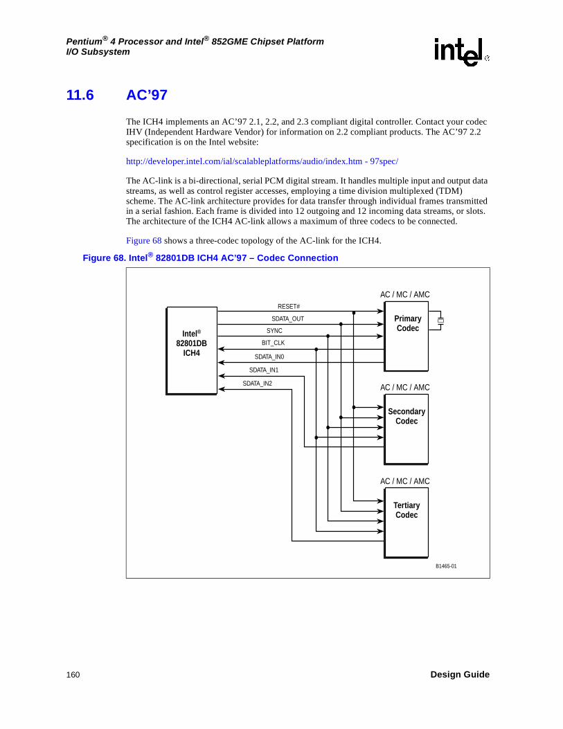
160 Design Guide
Pentium® 4 Processor and Intel® 852GME Chipset PlatformI/O Subsystem
11.6 AC’97
The ICH4 implements an AC’97 2.1, 2.2, and 2.3 compliant digital controller. Contact your codec IHV (Independent Hardware Vendor) for information on 2.2 compliant products. The AC’97 2.2 specification is on the Intel website:
http://developer.intel.com/ial/scalableplatforms/audio/index.htm - 97spec/
The AC-link is a bi-directional, serial PCM digital stream. It handles multiple input and output data streams, as well as control register accesses, employing a time division multiplexed (TDM) scheme. The AC-link architecture provides for data transfer through individual frames transmitted in a serial fashion. Each frame is divided into 12 outgoing and 12 incoming data streams, or slots. The architecture of the ICH4 AC-link allows a maximum of three codecs to be connected.
Figure 68 shows a three-codec topology of the AC-link for the ICH4.
Figure 68. Intel® 82801DB ICH4 AC’97 – Codec Connection
B1465-01
RESET#
SDATA_OUT
Intel®82801DB
ICH4
PrimaryCodec
AC / MC / AMC
AC / MC / AMC
SecondaryCodec
SYNC
BIT_CLK
SDATA_IN0
SDATA_IN1
SDATA_IN2
AC / MC / AMC
TertiaryCodec

Design Guide 161
Pentium® 4 Processor and Intel® 852GME Chipset PlatformI/O Subsystem
Note: When a modem codec is configured as the primary AC-link Codec, there should not be any Audio Codecs residing on the AC-link. The primary codec may be connected to AC_SDIN0 as documented in the Intel ICH4 Datasheet.
Clocking is provided from the primary codec on the link via AC_BIT_CLK, and is derived from a 24.576 MHz crystal or oscillator. Refer to the primary codec vendor for crystal or oscillator requirements. AC_BIT_CLK is a 12.288 MHz clock driven by the primary codec to the digital controller (ICH4) and to any other codec present. That clock is used as the time base for latching and driving data. Clocking AC_BIT_CLK directly off the CK-408 clock chip’s 14.31818 MHz output is not supported.
The ICH4 supports wake-on-ring from S1-S5 through the AC’97 link. The codec asserts AC_SDIN to wake the system. To provide wake capability and/or caller ID, standby power must be provided to the modem codec.
The ICH4 has weak pull-down/pull-ups that are always enabled. This keeps the link from floating when the AC-link is off or there are no codecs present.
When the Shut-off bit is not set, it implies that there is a codec on the link. Therefore, AC_BIT_CLK and AC_SDOUT are driven by the codec and the ICH4 respectively. However, AC_SDIN0, AC_SDIN1, and AC_SDIN2 may not be driven. When the link is enabled, the assumption may be made that there is at least one codec. Figure 69 presents the ICH4 AC’97 - AC_BIT_CLK topology.
Table 69 presents the AC’97 AC_BIT_CLK routing summary.
Figure 69. Intel® 82801DB ICH4 AC’97 – AC_BIT_CLK Topology
B1443-01
Intel®
82801DBICH4
AC_BIT_CLK
Primary Codec
CONN
L4L3L3L1
L2
R1 R2
Table 69. AC’97 AC_BIT_CLK Routing Summary
AC’97 Routing Requirements
Maximum Trace Length (inches)
Series Termination Resistance
AC_BIT_CLK Signal Length Matching
5 on 5
L1 = (1 to 8) – L3
L2 = 0.1 to 6
L3 = 0.1 to 0.4
L4 = (1 to 6) – L3
R1 = 33 Ω - 47 ΩR2 = Option 0 Ω resistor for debugging purposes
N/A
NOTES:1. Simulations were performed using the Analog Device* Codec (AD1885) and the Cirrus Logic* Codec
(CS4205b). Results showed that if the AD1885 codec was used a 33 Ω resistor was best for R1 and if the CS4205b codec was used a 47 Ω resistor for R1 was best.
2. Bench data shows that a 47 Ω resistor for R1 is best for the Sigmatel* 9750 codec.

162 Design Guide
Pentium® 4 Processor and Intel® 852GME Chipset PlatformI/O Subsystem
Figure 70 shows the ICH4 AC’97 - AC_SDOUT/AC_SYNC Topology.
Table 70 presents the AC’97 - AC_SDOUT/AC_SYNC routing summary.
Figure 71 shows the ICH4 AC’97 - AC_SDIN topology.
Figure 70. Intel® 82801DB ICH4 AC’97 – AC_SDOUT/AC_SYNC Topology
B1444-01
Intel®
82801DBICH4
AC_SDOUT
Primary Codec
CONN
L1L3L2
L4
L3
R1
R2
Table 70. AC’97 AC_SDOUT/AC_SYNC Routing Summary
AC’97 Routing Requirements
Maximum Trace Length (inches)
Series Termination Resistance
AC_SDOUT/AC_SYNC Signal Length Matching
5 on 5
L1 = (1 to 6) – L3
L2 = 1 to 8
L3 = 0.1 to 0.4
L4 = (0.1 to 6) – L3
R1 = 33 Ω - 47 ΩR2 = R1 if the connector card that will be used with the platform does not have a series termination on the card. Otherwise R2 = 0 Ω
N/A
NOTES:1. Simulations were performed using the Analog Device* Codec (AD1885) and the Cirrus Logic* Codec
(CS4205b). Results showed that if the AD1885 codec was used a 33 Ω resistor was best for R1 and if the CS4205b codec was used a 47 Ω resistor for R1 was best.
2. Bench data shows that a 47 Ω resistor for R1 is best for the Sigmatel* 9750 codec.
Figure 71. Intel® 82801DB ICH4 AC’97 – AC_SDIN Topology
B1371-01
Y1Y4 R2Y2
Y3
Y3
Y1R2
Y1R2
R1
Y5
Y1
Intel® 82801DBICH4
Codec
AC_SDIN1
AC_SDIN2
AC_SDIN0
AC97_SDATA_IN1
AC97_SDATA_IN2
AC97_SDATA_IN0
CONN

Design Guide 163
Pentium® 4 Processor and Intel® 852GME Chipset PlatformI/O Subsystem
Table 71 presents the AC’97 AC_SDIN routing summary.
11.6.1 AC’97 Routing
To ensure the maximum performance of the codec, proper component placement and routing techniques are required. These techniques include properly isolating the codec, associated audio circuitry, analog power supplies, and analog ground planes, from the rest of the motherboard. This includes plane splits and proper routing of signals not associated with the audio section. Contact your vendor for device-specific recommendations.
The basic recommendations are as follows:
• Special consideration must be given for the ground return paths for the analog signals.
• Digital signals routed in the vicinity of the analog audio signals must not cross the power plane split lines. Locate the analog and digital signals as far as possible from each other.
• Partition the board with all analog components grouped together in one area and all digital components in another.
• Provide separate analog and digital ground planes with the digital components over the digital ground plane, and the analog components, including the analog power regulators, over the analog ground plane. The split between planes must be a minimum of 0.05 inch wide.
• Keep digital signal traces, especially the clock, as far as possible from the analog input and voltage reference pins.
• Do not completely isolate the analog/audio ground plane from the rest of the board ground plane. Provide a single point (0.25 inch to 0.5 inch wide) where the analog/isolated ground plane connects to the main ground plane. The split between planes must be a minimum of 0.05 inch wide.
• Any signals entering or leaving the analog area must cross the ground split in the area where the analog ground is attached to the main motherboard ground. That is, no signal should cross the split/gap between the ground planes, which would cause a ground loop, thereby greatly increasing EMI emissions and degrading the analog and digital signal quality.
• Route analog power and signal traces over the analog ground plane.
• Route digital power and signal traces over the digital ground plane.
• Position the bypassing and decoupling capacitors close to the IC pins, or position the capacitors for the shortest connections to pins, with wide traces to reduce impedance.
Table 71. AC’97 AC_SDIN Routing Summary
AC’97 Routing Requirements
Maximum Trace Length (inches)
Series Termination Resistance
AC_SDIN Signal Length Matching
5 on 5
Y1 = 0.1 to 0.4
Y2 = (1 to 8) – Y1
Y3 = (1 to 14) – Y1
Y4 = (1 to 6) – Y1
Y5 = (0.1 to 6) – Y1
R1 = 33 Ω - 47 ΩR2 = R1 if the connector card that will be used with the platform does not have a series termination on the card. Otherwise R2 = 0 Ω
N/A
NOTES:1. Simulations were performed using the Analog Device* Codec (AD1885) and the Cirrus Logic* Codec
(CS4205b). Results showed that if the AD1885 codec was used a 33 Ω resistor was best for R1 and if the CS4205b codec was used a 47 Ω resistor for R1 was best.
2. Bench data shows that a 47 Ω resistor for R1 is best for the Sigmatel* 9750 codec.

164 Design Guide
Pentium® 4 Processor and Intel® 852GME Chipset PlatformI/O Subsystem
• All resistors in the signal path or on the voltage reference should be metal film. Carbon resistors may be used for DC voltages and the power supply path, where the voltage coefficient, temperature coefficient, and noise are not factors.
• Regions between analog signal traces should be filled with copper that should be electrically attached to the analog ground plane. Regions between digital signal traces should be filled with copper that should be electrically attached to the digital ground plane.
• Locate the crystal or oscillator close to the codec.
11.6.2 Motherboard Implementation
The following design considerations are provided for the implementation of an ICH4 platform using AC’97. These design guidelines have been developed to ensure maximum flexibility for board designers, while reducing the risk of board-related issues. These recommendations are not the only implementation or a complete checklist, but they are based on the ICH4 platform.
• Active components such as FET switches, buffers or logic states should not be implemented on the AC-link signals, except for AC_RST#. Doing so would potentially interfere with timing margins and signal integrity.
• The ICH4 supports wake-on-ring from S1M-S5 states via the AC’97 link. The codec asserts AC_SDIN to wake the system. To provide wake capability and/or caller ID, standby power must be provided to the modem codec. When no codec is attached to the link, internal pull-downs prevent the inputs from floating, so external resistors are not required.
• Route PC_BEEP through the audio codec. Care must be taken to avoid the introduction of a pop when powering the mixer up or down.
11.6.2.1 Valid Codec Configurations
Table 72 presents the supported codec configurations.
Table 72. Supported Codec Configurations
Option Primary Codec Secondary Codec Tertiary Codec Notes
1 Audio Audio Audio 1
2 Audio Audio Modem 1
3 Audio Audio Audio/Modem 1
4 Audio Modem Audio 1
5 Audio Audio/Modem Audio 1
6 Audio/Modem Audio Audio 1
NOTES:1. For power management reasons, codec power management registers are in audio space. As a result, if
there is an audio codec in the system it must be Primary.2. There cannot be two modems in a system since there is only one set of modem DMA channels.3. The ICH4 supports a modem codec on any of the AC-SDIN lines. However the modem codec ID must be
either 00 or 01.

Design Guide 165
Pentium® 4 Processor and Intel® 852GME Chipset PlatformI/O Subsystem
11.6.3 SPKR Pin Configuration
SPKR is used as both the output signal to the system speaker and as a functional strap. The strap function enables or disables the TCO Timer Reboot function based on the state of the SPKR pin on the rising edge of PWROK. When enabled, the ICH4 sends an SMI# to the processor upon a TCO timer timeout. The status of this strap is readable via the NO_REBOOT bit (bit 1, D31: F0, Offset D4h). The SPKR signal has a weak integrated pull-down resistor (the resistor is only enabled during boot/reset). Therefore, its default state is a logical zero or set to reboot. To disable the feature, a jumper may be populated to pull the signal line high (see Figure 72). The value of the pull-up must be such that the voltage divider output caused by the pull-up, the effective pull-down (Reff), and the ICH4’s integrated pull-down resistor are read as logic high (0.5 * VCC3_3 to VCC3_3 + 0.5 V).
Figure 72 shows the example speaker circuit.
11.7 CNR
Refer to the related documents, Communication and Network Riser Specification, Revision 1.2, available at http://developer.intel.com/technology/cnr/cnrspec_12.htm
The Communication and Networking Riser (CNR) Specification defines a hardware scalable OEM motherboard riser and interface. This interface supports multi-channel audio, V.90 analog modem, phone-line based networking, 10/100 Ethernet based networking, SMBus Interface Power Management Rev 1.1, and USB 2.0. The CNR specification defines the interface, which should be configured prior to shipment of the system. Standard I/O expansion slots, such as those supported by the PCI bus architecture, are intended to continue serving as the upgrade medium. The CNR mechanically shares a PCI slot, therefore the system designer will not sacrifice a PCI slot if he decides not to include a CNR in a particular build. Refer to the appropriate section of this document for the corresponding design and layout guidelines. The Platform LAN Connection (PLC) may be either an Intel® 82562EM or an Intel® 82562ET Platform LAN Connect component. Refer to the CNR specification for additional information.
Figure 72. Example Speaker Circuit
B1441-01
Intel®
82801DBICH4
Integratedpull-down
9 KΩ to50 KΩ
Effective impedancedue to speaker and
codec circuitReff
VCC3_3
SPKR
R value is implementation specific
Stuff the jumper to disable thetimeout feature (no reboot).

166 Design Guide
Pentium® 4 Processor and Intel® 852GME Chipset PlatformI/O Subsystem
Figure 73 shows the interface for the CNR connector.
11.7.1 AC’97 Audio Codec Detect Circuit and Configuration Options
Table 73 presents general circuits to implement a number of different codec configurations. Refer to the Communication and Network Riser Specification, Revision 1.2, for Intel’s recommended codec configurations.
11.7.2 CNR 1.2 AC’97 Disable and Demotion Rules for the Motherboard
The following are the CNR1.1/1.2 AC’97 Disable and Demotion Rules for the motherboard:
1. All AC’97 Revision 2.3 non-chaining. Codecs on the motherboard must always disable themselves when the CDC_DN_ENAB# signal is in a high state.
2. A motherboard AC’97 Codec must never change its address or SDATA_IN line used, regardless of the state of the CDC_DN_ENAB# signal.
3. On a motherboard containing an AC’97 Controller supporting three AC’97 Codecs, the AC’97 Revision 2.2, or AC’97 Revision 2.3 Codec on the motherboard, must be connected to the SDATA_IN2 signal of the CNR connector.
4. A motherboard should not contain more than a single AC’97 Codec.
These rules allow for forward and backward compatibility between CNR Version 1.1/1.2 cards.
Figure 73. CNR Interface
B1 4 42 -0 1
Com m unica tion andN etwork ing R iser
In te l®
8 2801D BICH 4
A C '97 In terface
LA N In terface
U S B 2.0
S M B us 1 .1
P o wer
R eserved
CN R Con nector
Table 73. Signal Descriptions
Signal Description
CDC_DN_ENAB#
When low, indicates that the codec on the motherboard is enabled and primary on the AC’97 interface. When high, indicates that the motherboard codec(s) must be removed from the AC’97 interface (held in reset), because the CNR coded(s) will be the primary device(s) on the AC’97 interface.
AC_RST# Reset signal from the AC’97 Digital Controller (ICH4).
AC_SDINn AC’97 serial data from an AC’97-compliant codec to an AC’97-compatible controller (that is, the ICH4).
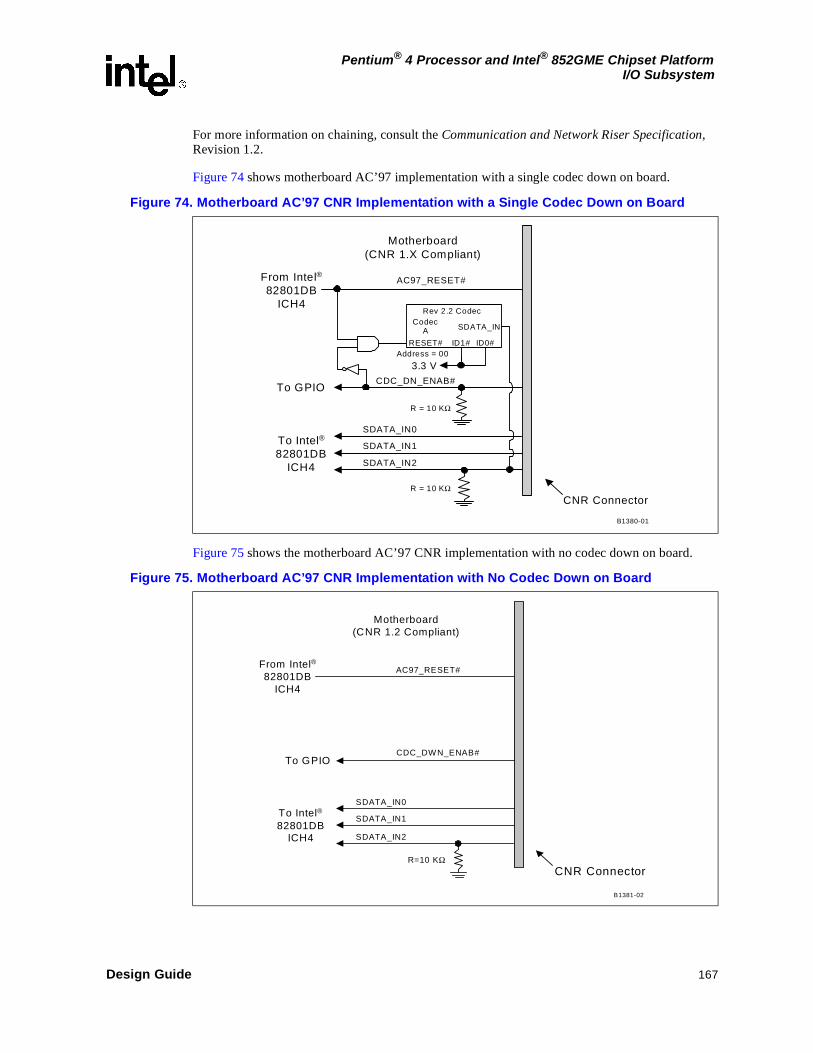
Design Guide 167
Pentium® 4 Processor and Intel® 852GME Chipset PlatformI/O Subsystem
For more information on chaining, consult the Communication and Network Riser Specification, Revision 1.2.
Figure 74 shows motherboard AC’97 implementation with a single codec down on board.
Figure 75 shows the motherboard AC’97 CNR implementation with no codec down on board.
Figure 74. Motherboard AC’97 CNR Implementation with a Single Codec Down on Board
Motherboard(CNR 1.X Compliant)
CNR Connector
SDATA_IN0
SDATA_IN1
SDATA_IN2
CDC_DN_ENAB#To GPIO
SDATA_IN
RESET# ID1# ID0#Address = 00
CodecA
3.3 V
R = 10 KΩ
Rev 2.2 Codec
R = 10 KΩ
From Intel®
82801DBICH4
AC97_RESET#
To Intel®
82801DBICH4
B1380-01
Figure 75. Motherboard AC’97 CNR Implementation with No Codec Down on Board
R=10 KΩCNR Connector
SDATA_IN0
SDATA_IN1
CDC_DWN_ENAB#
SDATA_IN2
Motherboard(CNR 1.2 Compliant)
To GPIO
AC97_RESET#From Intel®
82801DBICH4
To Intel®
82801DBICH4
B1381-02

168 Design Guide
Pentium® 4 Processor and Intel® 852GME Chipset PlatformI/O Subsystem
11.7.3 CNR Routing Summary
Table 74 presents a summary of the various interface routing requirements of the CNR riser.
11.8 USB 2.0 Guidelines and Recommendations
11.8.1 Layout Guidelines
11.8.1.1 General Routing and Placement
Use the following general routing and placement guidelines when laying out a new design. These guidelines help to minimize signal quality and EMI problems. The USB 2.0 validation efforts focused on a four-layer motherboard where the first layer is a signal layer, the second plane is power, the third plane is ground and the fourth is a signal layer. This results in the placement of most of the routing on the fourth plane (closest to the ground plane), allowing a higher component density on the first plane.
1. Place the ICH4 and major components on the un-routed board first. With minimum trace lengths, route high-speed clock, periodic signals, and USB 2.0 differential pairs first. Maintain maximum possible distance between high-speed clocks/periodic signals to USB 2.0 differential pairs and any connector leaving the PCB (that is, I/O connectors, control and signal headers, or power connectors).
2. Ground reference the USB 2.0 signals.
3. Route USB 2.0 signals using a minimum of vias and corners. This reduces reflections and impedance changes.
4. When it becomes necessary to turn 90°, use two 45° turns or an arc instead of making a single 90° turn. This reduces reflections on the signal by minimizing impedance discontinuities
5. Do not route USB 2.0 traces under crystals, oscillators, clock synthesizers, magnetic devices or IC’s that use and/or duplicate clocks.
6. Avoid stubs on high speed USB signals, as stubs cause signal reflections and affect signal quality. When a stub is unavoidable in the design, the sum of all stubs for a signal pair should not exceed 200 mils.
7. Route all traces over continuous planes (VCC or ground), with no interruptions. Avoid crossing over anti-etch if at all possible. Crossing over anti-etch (plane splits) increases inductance and
Table 74. CNR Routing Summary
CNR Routing Requirements Maximum Trace Length Signal Length Matching
Signal Referencing
USB (4 on 4.5) data pair must be at least 20 mils from nearest neighbor. 10 inches No more than 150 mils
trace mismatch. Ground
AC'97 (5 on 5)AC_BIT_CLK (See Table 69) AC_SDOUT (See Table 70) AC_SDIN (See Table 71)
N/A Ground
LAN (5 on 10) 9.5 inches (See Table 83)Equal to or up to 500 mils shorter than the LAN_CLK trace.
Ground

Design Guide 169
Pentium® 4 Processor and Intel® 852GME Chipset PlatformI/O Subsystem
radiation levels by forcing a greater loop area. Likewise, avoid changing layers with USB 2.0 traces as much as practical. It is preferable to change layers to avoid crossing a plane split.
8. Separate signal traces into similar categories and route similar signal traces together (such as routing differential pairs together).
9. Keep USB 2.0 USB signals clear of the core logic set. High current transients are produced during internal state transitions and may be very difficult to filter out.
10. Follow the 20*h rule by keeping traces at least 20*(height above the plane) away from the edge of the plane (VCC or ground, depending on the plane the trace is over). For the suggested stack-up the height above the plane is 4.5 mils. This calculates to a 90 mil spacing requirement from the edge of the plane. This helps prevent the coupling of the signal onto adjacent wires and also helps prevent free radiation of the signal from the edge of the PCB.
11.8.1.2 USB 2.0 Trace Separation
Use the following separation guidelines.
1. Maintain parallelism between USB differential signals with the trace spacing needed to achieve 90 Ω differential impedance. Deviations normally occur due to package breakout and routing to connector pins. Ensure the amount and length of the deviations are minimized.
2. Use an impedance calculator to determine the trace width and spacing required for the specific board stack-up being used. 4.0 mil traces with 4.5 mil spacing results in approximately 90 Ω differential trace impedance.
3. Minimize the length of high-speed clock and periodic signal traces that run parallel to high speed USB signal lines, to minimize crosstalk. Based on EMI testing experience, the minimum suggested spacing to clock signals is 50 mils.
4. Based on simulation data, use 20 mil minimum spacing between high-speed USB signal pairs and other signal traces for optimal signal quality. This helps to prevent crosstalk.
Figure 76 shows the recommended USB trace spacing.
Figure 76. Recommended USB Trace Spacing
B1467-02
5020
Distance in Mils
2044 4.5
Clock/High-SpeedPeriodic Signal
Low SpeedNon-periodic Signal DM1DP1
44 4.5
DM2DP2

170 Design Guide
Pentium® 4 Processor and Intel® 852GME Chipset PlatformI/O Subsystem
11.8.1.3 USBRBIAS Connection
The USBRBIAS pin and the USBRBIAS# pin may be shorted and routed 5 on 5 to one end of a 22.6 Ω ± 1% resistor to ground. Place the resistor within 500 mils of the ICH4 and avoid routing next to clock pins. Figure 77 shows the USBRBIAS connection.
Table 75 presents the USBRBIAS/USBRBIAS# routing summary.
11.8.1.4 USB 2.0 Termination
Use a common-mode choke to terminate the USB 2.0 bus. Place the common-mode choke as close as possible to the connector pins. See Section 11.8.4 for details.
11.8.1.5 USB 2.0 Trace Length Pair Matching
The USB 2.0 signal pair traces should be trace length matched. Maximum trace length mismatch between USB 2.0 signal pair should be no greater that 150 mils.
Figure 77. USBRBIAS Connection
Intel®
82801DBICH4
USBRBIAS
USBRBIAS#
22.6 Ω ±1%
B1382-01
Table 75. USBRBIAS/USBRBIAS# Routing Summary
USBRBIAS/ USBRBIAS# Routing Requirements Maximum Trace Length Signal Length Matching Signal Referencing
5 on 5 500 mils N/A N/A

Design Guide 171
Pentium® 4 Processor and Intel® 852GME Chipset PlatformI/O Subsystem
11.8.1.6 USB 2.0 Trace Length Guidelines
Table 76 presents the USB 2.0 trace length preliminary guidelines (with common-mode choke).
11.8.2 Plane Splits, Voids, and Cut-Outs (Anti-Etch)
The following guidelines apply to the use of plane splits voids and cutouts.
11.8.2.1 VCC Plane Splits, Voids, and Cut-Outs (Anti-Etch)
Use the following guidelines for the VCC plane.
1. Traces should not cross anti-etch, for it greatly increases the return path for those signal traces. This applies to USB 2.0 signals, high-speed clocks, and signal traces as well as slower signal traces that might be coupling to them. USB signaling is not purely differential in all speeds (that is, the Full-speed Single Ended Zero is common mode).
2. Avoid routing of USB 2.0 signals 25 mils of any anti-etch to avoid coupling to the next split or radiating from the edge of the PCB.
When breaking signals out from packages it is sometimes very difficult to avoid crossing plane splits or changing signal layers, particularly in today’s motherboard environment that uses several different voltage planes. Changing signal layers is preferable to crossing plane splits if a choice has to be made between one or the other.
Table 76. USB 2.0 Trace Length Preliminary Guidelines (With Common-mode Choke)
TopologyUSB 2.0 Routing Requirements/
Trace Impedance
SignalReferencing Signal Matching Cable
LengthMotherboard Trace Length
Card Trace
Length
Maximum Total
Length
Back Panel
4 on 4.5 / 90 Ωdifferential Ground
The maximum mismatch between data pairs should not be greater that 150 mils.
N/A 17 inches N/A 17 inches
CNR 4 on 4.5 / 90 Ωdifferential Ground N/A 8 inches 6 inches 14 inches
Front Panel
4 on 4.5 / 90 Ωdifferential Ground 9 6 2 17
10.5 5 2 17.5
12 4 2 18
13.5 3 2 18.5
15 2 2 19
NOTES:1. These lengths are based upon simulation results and may be updated in the future.2. All lengths are based upon using a common-mode choke (see Section 11.8.4 for details on common-mode choke).3. Numbers in this table are based on the following assumptions:-
a) CNR configuration: Maximum of six inch trace on add-on card.b) An approximate 1:1 trade-off may be assumed from Motherboard Trace Length vs. Daughter card Trace Length (for example, trade one inch of Daughter card for one inch of Motherboard Trace Lengths).
4. Numbers in the table are based on the following simulation assumptions:a) Trace length on front panel connector card assumed a maximum of two inches.b) USB twisted pair shielded cable as specified in USB 2.0 specification was used.

172 Design Guide
Pentium® 4 Processor and Intel® 852GME Chipset PlatformI/O Subsystem
When crossing a plane split is completely unavoidable, proper placement of stitching caps may minimize the adverse effects on EMI and signal quality performance caused by crossing the split. Stitching capacitors are small-valued capacitors (1 μF or lower in value) that bridge voltage plane splits close to where high speed signals or clocks cross the plane split. The capacitor ends should tie to each plane separated by the split. They are also used to bridge, or bypass, power and ground planes close to where a high-speed signal changes layers. As an example of bridging plane splits, a plane split that separates VCC5 and VCC3_3 planes should have a stitching cap placed near any high-speed signal crossing. Tie one side of the cap to VCC5 and the other side to VCC3_3. Stitching caps provide a high frequency current return path across plane splits. They minimize the impedance discontinuity and current loop area that crossing a plane split creates.
11.8.2.2 Ground Plane Splits, Voids, and Cut-Outs (Anti-Etch)
Avoid anti-etch on the ground plane.
11.8.3 USB Power Line Layout Topology
The following is a suggested topology for power distribution of Vbus to USB ports. Circuits of this type provide two types of protection during dynamic attach and detach situations on the bus: inrush current limiting (droop) and dynamic detach fly-back protection. These two different situations require both bulk capacitance (droop) and filtering capacitance (for dynamic detach fly-back voltage filtering). It is important to minimize the inductance and resistance between the coupling capacitors and the USB ports. That is, place capacitors as close as possible to the port and the power carrying traces should be as wide as possible, preferably, a plane. It is suggested to make the power carrying traces wide enough that the system fuse blows on an over-current event. When the system fuse is rated at 1 amp, the power carrying traces should be wide enough to carry at least 1.5 amps. Figure 78 shows the good downstream power connection.
Figure 78. Good Downstream Power Connection
B1162-01
5 VSwitch
5 V
5 V Sus
Thermister
220µF 470pF Port 1
VCC
GND
1
4
470pF Port 2
VCC
GND
1
4
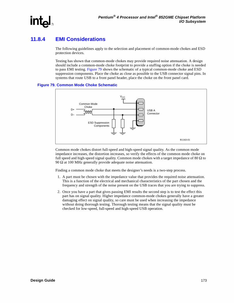
Design Guide 173
Pentium® 4 Processor and Intel® 852GME Chipset PlatformI/O Subsystem
11.8.4 EMI Considerations
The following guidelines apply to the selection and placement of common-mode chokes and ESD protection devices.
Testing has shown that common-mode chokes may provide required noise attenuation. A design should include a common-mode choke footprint to provide a stuffing option if the choke is needed to pass EMI testing. Figure 79 shows the schematic of a typical common-mode choke and ESD suppression components. Place the choke as close as possible to the USB connector signal pins. In systems that route USB to a front panel header, place the choke on the front panel card.
Common mode chokes distort full-speed and high-speed signal quality. As the common mode impedance increases, the distortion increases, so verify the effects of the common mode choke on full speed and high-speed signal quality. Common mode chokes with a target impedance of 80 Ω to 90 Ω at 100 MHz generally provide adequate noise attenuation.
Finding a common mode choke that meets the designer’s needs is a two-step process.
1. A part must be chosen with the impedance value that provides the required noise attenuation. This is a function of the electrical and mechanical characteristics of the part chosen and the frequency and strength of the noise present on the USB traces that you are trying to suppress.
2. Once you have a part that gives passing EMI results the second step is to test the effect this part has on signal quality. Higher impedance common-mode chokes generally have a greater damaging effect on signal quality, so care must be used when increasing the impedance without doing thorough testing. Thorough testing means that the signal quality must be checked for low-speed, full-speed and high-speed USB operation.
Figure 79. Common Mode Choke Schematic
B1163-01
VCC
Common ModeChoke
D–
ESD SuppressionComponents
USB AConnector
D+

174 Design Guide
Pentium® 4 Processor and Intel® 852GME Chipset PlatformI/O Subsystem
11.8.5 ESD
Classic USB (1.0/1.1) provided ESD suppression using in line ferrites and capacitors that formed a low-pass filter. This technique does not work for USB 2.0 due to the much higher signal rate of high-speed data. A device that has been tested successfully is based on spark gap technology. Proper placement of any ESD protection device is on the data lines between the common-mode choke and the USB connector data pins as shown in Figure 79. Other types of low-capacitance ESD protection devices may work as well but were not investigated. As with the common mode choke solution, it is recommended to include footprints for some type of ESD protection device as a stuffing option in case it is needed to pass ESD testing.
11.9 Front Panel Solutions
11.9.1 Internal USB Cables
The front panel internal cable solution chosen must meet all the requirements of Chapter 6 of the USB 2.0 Specification for high-/full-speed cabling for each port with the exceptions described in Cable Option 2.
11.9.1.1 Internal Cable Option 1
Use standard high-speed/full-speed compatible USB cables. These must meet all cabling requirements called out in Chapter 6 of the USB 2.0 specification. Recommended motherboard mating connector pin-out is covered in detail later in this document.
11.9.1.2 Internal Cable Option 2
Use custom cables that meet all of the requirements of Chapter 6 of the USB 2.0 specification with the following additions/exceptions:
• They may share a common jacket, shield and drain wire.
Two ports with signal pairs that share a common jacket may combine Vbus and ground wires into a single wire provided the following conditions are met:
• The bypass capacitance required by Section 7.2.4.1 of the USB 2.0 specification is physically located near the power and ground pins of the USB connectors. This is easiest to achieve by mounting the front panel USB connectors and the bypass capacitance on a small PCB (daughter card). Refer to the front panel daughter card referenced later for details.
• Selecting proper wire size: A general rule for replacing two power or ground wires with a single wire is to choose a wire size from Table 6-6 in Section 6.6.3 of the USB 2.0 specification that has = ½ the resistance of either of the two wires being combined. The data is provided for reference in Table 77.

Design Guide 175
Pentium® 4 Processor and Intel® 852GME Chipset PlatformI/O Subsystem
Table 77 presents the conductor resistance values.
Example 1. Replacing two 24-gauge (AWG) power or ground wires with one 20-gauge wire.
Proper wire gauge selection is important to meet the voltage drop and droop requirements called out in the USB 2.0 specification at the USB connectors as well as at the stake pins on the PCB.
Placing the capacitance near the USB connectors for cables that share power and ground conductors is required to ensure the system passes droop requirements. Cables that provide individual power and ground conductors for each port may usually meet droop requirements by providing adequate capacitance near the motherboard mating connector because droop is actually an effect felt by adjacent ports due to switching transients on the aggressor port. In the separate conductor case, all transients are detected and dampened by the capacitance at the motherboard mating connector before they may cause problems with the adjacent port sharing the same cable. See sections 7.2.2 and 7.2.4.1 of the USB 2.0 specification for more details.
Intel does not recommend cables that contain more than two signal pairs due to unpredictable impedance characteristics.
11.9.1.3 Motherboard/PCB Mating Connector
Proper selection of a motherboard mating connector for front panel USB support is important to ensure that signal quality is not adversely affected because of poor connector interface. The cable and PCB mating connector must also pass the TDR requirements listed in the USB 2.0 specification.
Table 77. Conductor Resistance Values
American Wire Gauge (AWG) Ohm (Ω) / 100 Meters maximum
28 23.20
26 14.60
24 9.09
22 5.74
20 3.58
NOTE: This information is available in Table 6-6 of the Universal Serial Bus 2.0 Specification.

176 Design Guide
Pentium® 4 Processor and Intel® 852GME Chipset PlatformI/O Subsystem
11.9.1.3.1 Pin-out
A ten pin, 0.1-inch pitch stake pin assembly is recommended with the pin-out listed in Table 78 and shown in Figure 80.
Intel recommends that the fuse element (thermistor) for the front panel header be included on the motherboard to protect the motherboard from damage.
• This protects the motherboard from damage in the case where an un-fused front panel cable solution is used.
• It also provides protection from damage if an un-keyed cable is inadvertently plugged onto the front panel USB connector.
• It provides protection to the motherboard in the case where the front panel cable is cut or damaged during assembly or manufacturing resulting in a short between Vbus and ground.
Table 78. Front Panel Header Pin-Out
Pin Description
1 Vcc
2 Vcc
3 dm1
4 dp1
5 dm2
6 dp2
7 Ground
8 Ground
9 key
10 No connect or over-current sense
Figure 80. Front Panel Header Schematic
B
KEY
DM1
DP1
THRMSTR 1.5Afor two ports
120µF Per Hub
GND
DM2
DP2
GND
NC or Overcurrent
Cbypass
Vbus
VCC
3 4
1 2
5 6
7 8
9 10

Design Guide 177
Pentium® 4 Processor and Intel® 852GME Chipset PlatformI/O Subsystem
11.9.1.4 Routing Considerations
Traces or surface shapes from VCC to the thermistor, to Cbypass and to the connector power and ground pins should be at least 50 mils wide to ensure adequate current carrying capability.
Provide or verify the presence of double vias on power and ground nets, and keep the trace lengths as short as possible.
11.9.1.5 Front Panel Connector Card
The recommended way to provide front or side panel support for USB is to use a daughter card and cable assembly. This allows the placement of the EMI/ESD suppression components right at the USB connector where they are the most effective. Figure 81 shows the major components associated with a typical front/side panel USB solution that uses a front panel connector card.
Note: The terms connector card and daughter card are used interchangeably. When designing the motherboard with front/side panel support, the system integrator should identify the type of cable assembly to be used. When the system integrator plans to use a connector card, ensure that there are not duplicate EMI/ESD/thermistor components placed on the motherboard because this usually causes drop/droop and signal quality degradation or failure.
11.9.1.6 Front Panel Daughter Card Design Guidelines
• Place the Vbus bypass capacitance, Common Mode Choke, and ESD suppression components on the daughter card as close as possible to the connector pins.
• Follow the same layout, routing and impedance control guidelines as specified for motherboards.
• Minimize the trace length on the front panel connector card. Less than two-inch trace length is recommended.
• Use the same mating connector pin-out as outlined for the motherboard in Section 11.9.1.3.1.
• Use the same routing guidelines as described in Section 11.8.1.
• Trace length guidelines are presented in Table 76.
Figure 81. Motherboard Front Panel USB Support
B1165-01
Motherboard Front Panel USB Ports

178 Design Guide
Pentium® 4 Processor and Intel® 852GME Chipset PlatformI/O Subsystem
11.10 IOAPIC (I/O Advanced Programmable Interrupt Controller)
The Intel® 852GME chipset platform does not support IOAPIC when C2/C3/C4 states are enabled.
11.10.1 IOAPIC Disabling Options (Recommended Implementation)
Intel recommends that IOAPIC be disabled in software while the connections to the board are as shown in Figure 82. Software may be used to turn off PICCLK from clock generator.
To disable IOAPIC in BIOS:
1. ICH4: D31:F0; Offset: D1; bit 0 (0=disable);
2. Pentium® 4 processor: MSR 1Bh bit 11 (0 = Disable)
UP systems not using the IOAPIC Bus should follow these recommendations:
On the ICH4:
3. Tie APICCLK directly to ground.
4. Tie APICD0, APICD1 to ground through a 10 kΩ resistor (separate pull-downs are required if using XOR chain testing).
Figure 82 shows the minimum IOAPIC disable topology.
Figure 82. Minimum IOAPIC Disable Topology
B1383-01
CK-408
PCIF0
Intel®82801DB
ICH4
APICD0
APICLKAPICD1
33 Ω

Design Guide 179
Pentium® 4 Processor and Intel® 852GME Chipset PlatformI/O Subsystem
11.10.2 PIRQ Routing Example
Table 79 presents how the ICH4 uses the PCI IRQ when the IOAPIC is active.
Due to different system configurations, IRQ line routing to the PCI slots (swizzling) should be made to minimize sharing of interrupts between both internal ICH4 functions and PCI functions.
Note: It is not necessarily an optimal routing scheme; an optimal scheme depends on individual system PCI IRQ usage.
Figure 83 shows an example of IRQ line routing to the PCI slots.
Figure 83 is an example. It is up to board designers to route these signals in a way that proves the most efficient for their particular system. A PCI slot may be routed to share interrupts with any of the ICH4’s internal device/functions, but at a higher latency cost.
Table 79. IOAPIC Interrupt Inputs 16 Through 23 Usage
Number IOAPIC INTIN Pin Function in Intel® ICH4 Using the PCI IRQ in IOAPIC
1 IOAPIC INTIN PIN 16 (PIRQA) USB UHCI Controller #1
2 IOAPIC INTIN PIN 17 (PIRQB) AC’97 Audio and Modem; option for SMBus
3 IOAPIC INTIN PIN 18 (PIRQC) USB UHCI Controller #3; Native IDE
4 IOAPIC INTIN PIN 19 (PIRQD) USB UHCI Controller #2
5 IOAPIC INTIN PIN 20 (PIRQE) Internal LAN; option for SCI, TCO, MMT #0,1,2
6 IOAPIC INTIN PIN 21 (PIRQF) Option for SCI, TCO, MMT #0,1,2
7 IOAPIC INTIN PIN 22 (PIRQG) Option for SCI, TCO, MMT #0,1,2
8 IOAPIC INTIN PIN 23 (PIRQH) USB EHCI Controller, Option for SCI, TCO, MMT #0,1,2
Figure 83. Example PIRQ Routing
B1472-01
INTA
INTB
INTC
INTD
PIRQA#PIRQB#PIRQC#PIRQD#
PIRQE#
PIRQF#
PIRQG#PIRQH#
Intel®82801DB
ICH4
SLOT 1PCI Device 0
(AD16 to IDSEL)
SLOT 2PCI Device 5
(AD21 to IDSEL)
SLOT 3PCI Device 6
(AD22 to IDSEL)
SLOT 4PCI Device C
(AD28 to IDSEL)
INTA
INTB
INTC
INTD
INTA
INTB
INTC
INTD
INTA
INTB
INTC
INTD
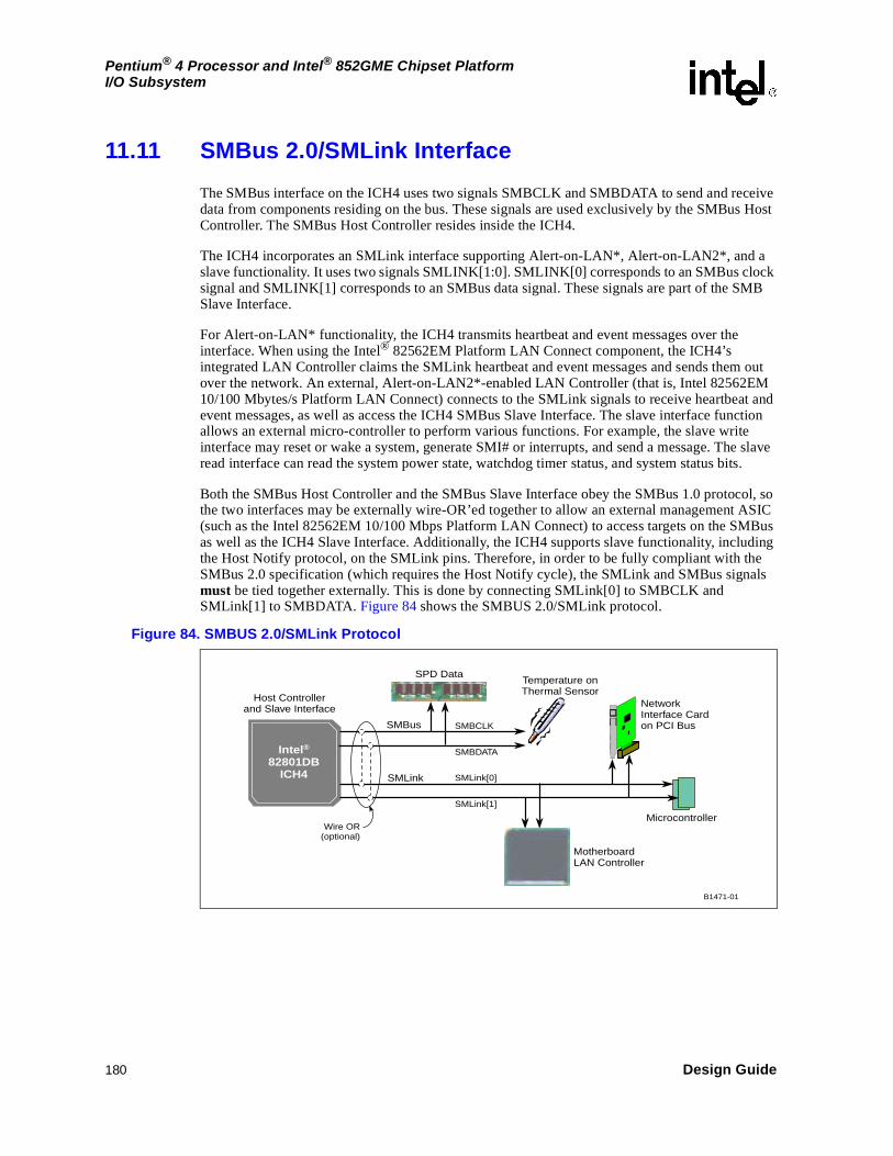
180 Design Guide
Pentium® 4 Processor and Intel® 852GME Chipset PlatformI/O Subsystem
11.11 SMBus 2.0/SMLink Interface
The SMBus interface on the ICH4 uses two signals SMBCLK and SMBDATA to send and receive data from components residing on the bus. These signals are used exclusively by the SMBus Host Controller. The SMBus Host Controller resides inside the ICH4.
The ICH4 incorporates an SMLink interface supporting Alert-on-LAN*, Alert-on-LAN2*, and a slave functionality. It uses two signals SMLINK[1:0]. SMLINK[0] corresponds to an SMBus clock signal and SMLINK[1] corresponds to an SMBus data signal. These signals are part of the SMB Slave Interface.
For Alert-on-LAN* functionality, the ICH4 transmits heartbeat and event messages over the interface. When using the Intel® 82562EM Platform LAN Connect component, the ICH4’s integrated LAN Controller claims the SMLink heartbeat and event messages and sends them out over the network. An external, Alert-on-LAN2*-enabled LAN Controller (that is, Intel 82562EM 10/100 Mbytes/s Platform LAN Connect) connects to the SMLink signals to receive heartbeat and event messages, as well as access the ICH4 SMBus Slave Interface. The slave interface function allows an external micro-controller to perform various functions. For example, the slave write interface may reset or wake a system, generate SMI# or interrupts, and send a message. The slave read interface can read the system power state, watchdog timer status, and system status bits.
Both the SMBus Host Controller and the SMBus Slave Interface obey the SMBus 1.0 protocol, so the two interfaces may be externally wire-OR’ed together to allow an external management ASIC (such as the Intel 82562EM 10/100 Mbps Platform LAN Connect) to access targets on the SMBus as well as the ICH4 Slave Interface. Additionally, the ICH4 supports slave functionality, including the Host Notify protocol, on the SMLink pins. Therefore, in order to be fully compliant with the SMBus 2.0 specification (which requires the Host Notify cycle), the SMLink and SMBus signals must be tied together externally. This is done by connecting SMLink[0] to SMBCLK and SMLink[1] to SMBDATA. Figure 84 shows the SMBUS 2.0/SMLink protocol.
Figure 84. SMBUS 2.0/SMLink Protocol
B1471-01
SMBus
Host Controllerand Slave Interface Network
Interface Cardon PCI Bus
Temperature onThermal Sensor
SPD Data
Microcontroller
MotherboardLAN Controller
SMBDATA
SMBCLK
SMLink[1]
SMLink[0]
Intel®82801DB
ICH4 SMLink
Wire OR(optional)

Design Guide 181
Pentium® 4 Processor and Intel® 852GME Chipset PlatformI/O Subsystem
Note: Intel does not support external access of the ICH4’s Integrated LAN Controller through the SMLink interface. Also, Intel does not support access of the ICH4’s SMBus Slave Interface by the ICH4’s SMBus Host Controller. Refer to the Intel 82801DB I/O Controller Hub 4 Datasheet for full functionality descriptions of the SMLink and SMBus interface.
11.11.1 SMBus Architecture and Design Considerations
11.11.1.1 SMBus Design Considerations
There is not a single SMBus design solution that works for all platforms. The system designer must consider the total bus capacitance and device capabilities when designing SMBus segments. Routing SMBus to the PCI slots makes the design process even more challenging since they add extra capacitance to the bus. This extra capacitance has a large affect on the bus time constant, which in turn affects the bus rise and fall times.
Primary considerations in the design process are:
1. Device class (high/low power). Most designs use primarily high power devices.
2. Are there devices that must run in S3?
3. Amount of VCC_SUSPEND current available (that is, minimizing load of VCC_ SUSPEND).
11.11.1.2 General Design Issues/Notes
Regardless of the architecture used, there are some general considerations.
1. The pull-up resistor size for the SMBus data and clock signals is dependent on the bus load (this includes all device leakage currents). Generally, the SMBus device that may sink the least amount of current is the limiting agent on how small the resistor may be. The pull-up resistor cannot be made so large that the bus time constant (resistance times capacitance) does not meet the SMBus rise and fall time specification.
2. The maximum bus capacitance that a physical segment may reach is 400 pF.
3. The ICH4 does not run SMBus cycles while in S3.
4. SMBus devices that may operate in S3 must be powered by the VCC_ SUSPEND supply.
5. When SMBus is to be connected to PCI, it must be connected to all PCI slots.

182 Design Guide
Pentium® 4 Processor and Intel® 852GME Chipset PlatformI/O Subsystem
11.11.2 Power Supply Considerations
11.11.2.1 Unified VCC_ Suspend Architecture
In this design all SMBus devices are powered by the VCC_Suspend supply. Consideration must be made to provide enough VCC_Suspend current while in S3. Figure 85 shows the unified VCC_Suspend architecture.
11.11.2.1.1 Unified VCC_CORE Architecture
In this design, all SMBUS devices are powered by the VCC_CORE supply. This architecture allows none of the devices to operate in S3, but minimizes the load on VCC_Suspend. Figure 86 shows the unified VCC_CORE architecture.
NOTES:1. The SMBus device must be back-drive safe while its supply (Vcore) is off and VCC_Suspend is still powered.2. In suspended modes where VCC_CORE is off and VCC_Suspend is on, the VCC_CORE node is very near
ground. In this case, the input leakage of the ICH4 is approximately 10 µA.
Figure 85. Unified VCC_Suspend Architecture
B1569-01
SMBusDevices
Intel®82801DB
ICH4
VccSus3_3
VccSus
VccSus3_3
SMBus
Figure 86. Unified VCC_CORE Architecture
B1570-01
SMBusDevices
Intel®82801DB
ICH4
VccSus3_3
Vcc
VccSus3_3
SMBus

Design Guide 183
Pentium® 4 Processor and Intel® 852GME Chipset PlatformI/O Subsystem
11.11.2.1.2 Mixed Power Supply Architecture
This design allows for SMBus devices to communicate while in S3, yet minimizes VCC_Suspend leakage by keeping non-essential devices on the core supply. This is accomplished by the use of a bus switch to isolate the devices powered by the core and suspend supplies. Figure 87 shows the mixed VCC_Suspend/VCC_CORE architecture.
11.11.2.2 Device Class Considerations
In addition to the power supply considerations described above, system designers should take into consideration the SMBus device class (high power/low power) used on the bus. When the design supports both high-power and low-power devices on the bus, current isolation of high-power segment and low-power segment of the bus is needed as shown in Figure 88.
Figure 87. Mixed VCC_Suspend/VCC_CORE Architecture
B1369-01
VccSus3_3 VccVccSus
VccSusVccSus3_3
SMBusSMBus
OE#SLP_S3#
VccSus
Devices Runningin Standby
Vcc Vcc
Non-StandbyDevices
BusSwitch
Intel®
82801DBICH4
Figure 88. High Power/Low Power Mixed VCC_SUSPEND/VCC_CORE Architecture
B1372-01
Vcc VccSus3_3
BusSwitch
BusSwitch
Intel®
82801DBICH4
CurrentIsolationCircuit
VccVccSus3_3Vcc
VccSus
Non StandbyDevices
VccSus
SMBusSMBusSMBus
OE#SLP_S3#
VccVccSus VccSus
OE#SLP_S3#
Non StandbyDevices
Devices Runningin Standby
Devices Runningin Standby
LowCurrent
HighCurrent

184 Design Guide
Pentium® 4 Processor and Intel® 852GME Chipset PlatformI/O Subsystem
11.12 FWH
The following provides general guidelines for compatibility and design recommendations for supporting the FWH device. The majority of the changes will be incorporated in the BIOS. Refer to the FWH BIOS Specification or equivalent.
11.12.1 FWH Decoupling
Place a 0.1 µF capacitor between the VCC supply pins and the VSS ground pins to decouple high frequency noise, which may affect the programmability of the device. Additionally, place a 4.7 µF capacitor between the VCC supply pins and the VSS ground pins to decouple low frequency noise. Place the capacitors no further than 390 mils from the VCC supply pins.
11.12.2 In-circuit FWH Programming
All cycles destined for the FWH will appear on PCI. The ICH4 Hub Interface to PCI Bridge puts all CPU boot cycles out on PCI (before sending them out on the FWH interface). When the ICH4 is set for subtractive decode, these boot cycles may be accepted by a positive decode agent on the PCI bus. This enables the ability to boot from a PCI card that positively decodes these memory cycles. In order to boot from a PCI card, it is necessary to keep the ICH4 in subtractive decode mode. When a PCI boot card is inserted and the ICH4 is programmed for positive decode, there are two devices positively decoding the same cycle.
11.12.3 FWH INIT# Voltage Compatibility
The FWH INIT# signal trip points need to be considered because they are NOT consistent among different FWH manufacturers. The INIT# signal is active low. Therefore, the inactive state of the ICH4 INIT# signal needs to be at a value slightly higher than the VIH min FWH INIT# pin specification. The inactive state of this signal is typically governed by the formula V_CPU_IO(min) – noise margin. Therefore, if the V_CPU_IO(min) of the processor is 1.60 V, the noise margin is 200 mV and the VIH min spec of the FWH INIT# input signal is 1.35 V, there would be no compatibility issue because 1.6 V - 0.2 V = 1.40 V, which is greater than the 1.35 V minimum of the FWH. If the VIH min of the FWH was 1.45 V, there would be an incompatibility and logic translation would need to be used. The examples above do not take into account any noise that may be encountered on the INIT# signal. Ensure that the VIH min specification is met with ample noise margin. In applications where it is necessary, use translation logic.
The solution assumes that level translation is necessary. It is strongly recommended that any system that implements a FWH should have its INIT# input connected to the ICH4.
11.12.4 FWH VPP Design Guidelines
The VPP pin on the FWH is used for programming the flash cells. The FWH supports VPP of 3.3 V or 12 V. When VPP is 12 V, the flash cells program about 50% faster than at 3.3 V. However, the FWH only supports 12 V VPP for 80 hours (3.3 V on Vpp does not affect the life of the device). The 12 V VPP would be useful in a programmer environment, which is typically an event that occurs very infrequently (much less than 80 hours). The VPP pin MUST be tied to 3.3 V on the motherboard.

Design Guide 185
Pentium® 4 Processor and Intel® 852GME Chipset PlatformI/O Subsystem
In some cases, it is desirable to program the FWH during assembly with the device soldered on the board. To decrease programming time, it becomes necessary to apply 12 V to the VPP pin. The following circuit allows testers to put 12 V on the VPP pin while keeping the voltage separate from the 3.3 V plane to which the rest of the power pins are connected. This circuit also allows the board to operate with 3.3 V on the pin during normal operation. Figure 89 shows the FWH VPP isolation circuitry.
11.13 RTC
The ICH4 contains a real time clock (RTC) with 256 bytes of battery backed SRAM. The internal RTC module provides two key functions: keeping date and time and storing system data in its RAM when the system is powered down.
The ICH4 uses a crystal circuit to generate a low-swing, 32 KHz input sine wave. This input is amplified and driven back to the crystal circuit via the RTCX2 signal. Internal to the ICH4, the RTCX1 signal is amplified to drive internal logic as well as generate a free-running, full-swing clock output for system use. The ICH4 output ball is labeled SUSCLK, as shown in Figure 90.
For further information on the RTC, consult Application Note AP-728 ICH/ICH2/ICH2M/ICH4S/ICH4M Real Time Clock (RTC) Accuracy and Considerations Under Test Conditions. This application note is valid for the ICH4.
Even if the ICH4 internal RTC is not used, it is still necessary to supply a clock input to RTCX1 of the ICH4 because other signals are gated off that clock in suspend modes. However, in this case the frequency accuracy (32.768 KHz) of the clock inputs is not critical; a crystal may be used or a single clock input may be driven into RTCX1 with RTCX2 left as no connect (Figure 91 shows this connection).
Figure 89. FWH VPP Isolation Circuitry
B1191-01
FET
1 KΩ
(from Motherboard)
VPP
3.3 V12 V
Figure 90. RTCX1 and SUSCLK Relationship in the Intel® 82801DB ICH4
B1470-01
InternalOscillator
Low-Swing 32.768 kHzSine Wave Source
Full-Swing 32.768 kHzOutput Signal
Intel®82801DB
ICH4
RTCX1
SUSCLK

186 Design Guide
Pentium® 4 Processor and Intel® 852GME Chipset PlatformI/O Subsystem
Note: This is not a validated feature on the ICH4. The peak-to-peak swing on RTCX1 cannot exceed 1.0 V.
Figure 91 shows the external circuitry for the ICH4 where the internal RTC is not used.
11.13.1 RTC Crystal
The ICH4 RTC module requires an external oscillating source of 32.768 KHz connected on the RTCX1 and RTCX2 balls. Figure 92 shows the external circuitry that comprises the oscillator of the ICH4 RTC.
Figure 91. External Circuitry for the Intel® 82801DB ICH4 Where the Internal RTCis Not Used
B1181-01
NoConnection
5 MΩRTCX2 Internal
External
RTCX1
32 kHz
Figure 92. External Circuitry for the Intel® 82801DB ICH4 RTC
B1469-01
C218pF
C118pF
Vbatt
R110MΩ
1kΩ32.768 kHz
Xtal
1µF
VCCRTC3.3v Sus
C30.047µF
+–
RTCX2
RTCX1
R210MΩ
VBIAS
Reference Designators arbitrarily assigned 3.3V Sus is active whenever system plugged in Vbatt is voltage provided by battery.
VBIAS, VCCRTC, RTCX1, and RTCX2 are ICH4 pins.VBIAS is used to bias the ICH4 internal oscillator.VCCRTC powers the RTC well of the ICH4.RTCX1 is the input to the internal oscillator.RTCX2 is the feedback for the external crystal.
Notes:1. The exact capacitor value needs to be based on what the crystal maker recommends. (Typical values
for C2 and C3 are 18 pF, based on crystal load of 12.5 pF.2. VCCRTC: Power for RTC Well.3. RTCX2: Crystal Input 2 - Connected to the 32.7 68-kHz crystal.4. RTCX1: Crystal Input 1 - Connected to the 32.7 68-kHz crystal.5 VBIAS: RTC BIAS Voltage - This ball is used to provide a reference voltage, and this CD voltage sets a
current which is mirrored throughout the oscillator and buffer circuitry.6. VSS: Ground

Design Guide 187
Pentium® 4 Processor and Intel® 852GME Chipset PlatformI/O Subsystem
Table 80 presents the RTC routing summary.
11.13.2 External Capacitors
To maintain the RTC accuracy, the external capacitor C3 needs to be 0.047 µF and capacitor values C1 and C2 should be chosen to provide the manufacturer’s specified load capacitance (Cload) for the crystal when combined with the parasitic capacitance of the trace, socket (if used), and package. Equation 3 may be used to choose the external capacitance values:
Equation 3. External Capacitance Values
Where:
• Cload = Crystal’s load capacitance. This value may be obtained from Crystal’s specification.
• Cin1, Cin2 = input capacitances at RTCX1, RTCX2 balls of the ICH4. These values may be obtained in the ICH4’s Datasheet.
• Ctrace1, Ctrace2 = Trace length capacitances measured from Crystal terminals to RTCX1, RTCX2 balls. These values depend on the characteristics of board material, the width of signal traces and the length of the traces. A typical value, based on a 5 mil wide trace and a ½ ounce copper pour, is approximately equal to: Ctrace = trace length * 2 pF/inch
• Cparasitic = Crystal’s parasitic capacitance. This capacitance is created by the existence of two electrode plates and the dielectric constant of the crystal blank inside the Crystal part. Refer to the crystal’s specification to obtain this value.
Ideally, C1, C2 may be chosen such that C1 = C2. Using the equation of Cload above, the value of C1, C2 may be calculated to give the best accuracy (closest to 32.768 KHz) of the RTC circuit at room temperature. However, C2 may be chosen such that C2 > C1. Then C1 may be trimmed to obtain the 32.768 KHz.
In certain conditions, both C1, C2 values may be shifted away from the theoretical values (calculated values from the above equation) to obtain the closest oscillation frequency to 32.768 KHz. When C1, C2 values are smaller then the theoretical values, the RTC oscillation frequency are higher.
Table 80. RTC Routing Summary
RTC RoutingRequirements
Maximum Trace Length
To Crystal
Signal Length
MatchingR1, R2, C1, and C2 Tolerances Signal
Referencing
5 mil trace width(results in ~2 pF per inch) 1 inch N/A
R1 = R2 = 10 MΩ ± 5%
C1 = C2 = (NPO class)
See Section 11.13.2 for calculating a specific capacitance value for C1 and C2.
Ground
Cload C1 Cin1 Ctrace1 )+ +([ ] C2 Cin2 Ctrace2+ +( )[ ] C1 Cin1 Ctrace1 C2 Cin2 Ctrace2+ + + )+ +([ ] Cparasitic+⁄×=

188 Design Guide
Pentium® 4 Processor and Intel® 852GME Chipset PlatformI/O Subsystem
The following example illustrates the use of the practical values C1, C2 in the case that theoretical values cannot ensure the accuracy of the RTC in low temperature condition.
Example 2. Use of Practical Values C1 and C2 when Theoretical Values Cannot Ensure the Accuracy of the RTC in Low Temperatures
According to a required 12 pF load capacitance of a typical crystal that is used with the ICH4, the calculated values of C1 = C2 is 10 pF at room temperature (25°C) to yield a 32.768 KHz oscillation.
At 0° C, the frequency stability of crystal gives – 23 ppm (assumed that the circuit has 0 ppm at 25°C). This makes the RTC circuit oscillate at 32.767246 KHz instead of 32.768 KHz.
When the values of C1, C2 are chosen to be 6.8 pF instead of 10 pF, the RTC oscillates at a higher frequency at room temperature (+23 ppm). However, this configuration of C1 / C2 makes the circuit oscillate closer to 32.768 KHz at 0° C. The 6.8 pF value of C1 and 2 is the practical value.
Note: The temperature dependency of crystal frequency is a parabolic relationship (ppm/degree square). The effect of changing the crystal’s frequency when operating at 0° C (25° C below room temperature) is the same when operating at 50° C (25° C above room temperature).
11.13.3 RTC Layout Considerations
Since the RTC circuit is very sensitive and requires high accuracy oscillation, reasonable care must be taken during layout and routing of the RTC circuit. Some recommendations are:
1. Reduce trace capacitance by minimizing the RTC trace length. The ICH4 requires a trace length less than one inch on each branch (from crystal’s terminal to RTCXn ball). Routing the RTC circuit should be kept simple to simplify the trace length measurement and increase accuracy on calculating trace capacitances. Trace capacitance depends on the trace width and dielectric constant of the board’s material. On FR-4, a 5 mil trace has approximately 2 pF per inch.
2. Trace signal coupling must be limited as much as possible by avoiding the routing of adjacent PCI signals close to RTCX1 and RTCX2, and VBIAS.
3. Intel recommends a ground guard plane.
4. The oscillator VCC should be clean; use a filter, such as an RC low-pass, or a ferrite inductor.
11.13.4 RTC External Battery Connections
The RTC requires an external battery connection to maintain its functionality and its RAM while the ICH4 is not powered by the system.
Example batteries are: Duracell* 2032, 2025, or 2016 (or equivalent) that may give many years of operation. Batteries are rated by storage capacity. The battery life may be calculated by dividing the capacity by the average current required. For example, if the battery storage capacity is 170 mAh (assumed usable) and the average current required is 5 µA, the battery life is at least:
170,000 µAh / 5 µA = 34,000 h = 3.9 years
The voltage of the battery may affect the RTC accuracy. In general, when the battery voltage decays, the RTC accuracy also decreases. High accuracy may be obtained when the RTC voltage is in the range of 3.0 V to 3.3 V.

Design Guide 189
Pentium® 4 Processor and Intel® 852GME Chipset PlatformI/O Subsystem
The battery must be connected to the ICH4 through a Schottky diode circuit for isolation. The Schottky diode circuit allows the ICH4 RTC-well to be powered by the battery when the system power is not available, but by the system power when it is available. To do this, the diodes are set to be reverse biased when the system power is not available. Figure 93 is an example of a diode circuit that is used.
A standby power supply should be used in a mobile system to provide continuous power to the RTC when available, which significantly increases the RTC battery life and thereby the RTC accuracy.
Figure 93. Diode Circuit to Connect RTC External Battery
B1474-02
1 KΩ
VCCRTC
VCCSUS3_3
1.0 µF
Battery+–
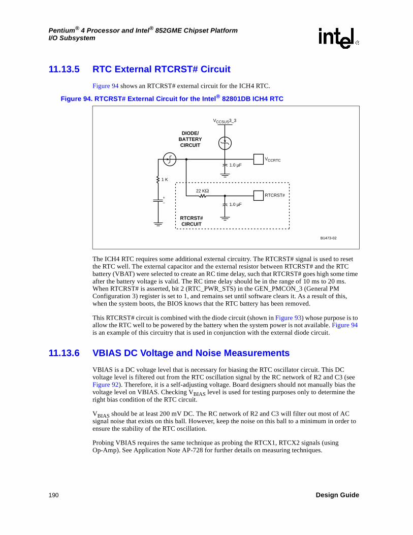
190 Design Guide
Pentium® 4 Processor and Intel® 852GME Chipset PlatformI/O Subsystem
11.13.5 RTC External RTCRST# Circuit
Figure 94 shows an RTCRST# external circuit for the ICH4 RTC.
The ICH4 RTC requires some additional external circuitry. The RTCRST# signal is used to reset the RTC well. The external capacitor and the external resistor between RTCRST# and the RTC battery (VBAT) were selected to create an RC time delay, such that RTCRST# goes high some time after the battery voltage is valid. The RC time delay should be in the range of 10 ms to 20 ms. When RTCRST# is asserted, bit 2 (RTC_PWR_STS) in the GEN_PMCON_3 (General PM Configuration 3) register is set to 1, and remains set until software clears it. As a result of this, when the system boots, the BIOS knows that the RTC battery has been removed.
This RTCRST# circuit is combined with the diode circuit (shown in Figure 93) whose purpose is to allow the RTC well to be powered by the battery when the system power is not available. Figure 94 is an example of this circuitry that is used in conjunction with the external diode circuit.
11.13.6 VBIAS DC Voltage and Noise Measurements
VBIAS is a DC voltage level that is necessary for biasing the RTC oscillator circuit. This DC voltage level is filtered out from the RTC oscillation signal by the RC network of R2 and C3 (see Figure 92). Therefore, it is a self-adjusting voltage. Board designers should not manually bias the voltage level on VBIAS. Checking VBIAS level is used for testing purposes only to determine the right bias condition of the RTC circuit.
VBIAS should be at least 200 mV DC. The RC network of R2 and C3 will filter out most of AC signal noise that exists on this ball. However, keep the noise on this ball to a minimum in order to ensure the stability of the RTC oscillation.
Probing VBIAS requires the same technique as probing the RTCX1, RTCX2 signals (using Op-Amp). See Application Note AP-728 for further details on measuring techniques.
Figure 94. RTCRST# External Circuit for the Intel® 82801DB ICH4 RTC
B1473-02
1 K
VCCRTC
VCCSUS3_3
1.0 µF
1.0 µF
22 KΩ
RTCRST#CIRCUIT
DIODE/BATTERYCIRCUIT
+–
RTCRST#

Design Guide 191
Pentium® 4 Processor and Intel® 852GME Chipset PlatformI/O Subsystem
Note: VBIAS is also very sensitive to environmental conditions.
11.13.7 SUSCLK
SUSCLK is a square waveform signal output from the RTC oscillation circuit. Depending on the quality of the oscillation signal on RTCX1 (largest voltage swing), SUSCLK duty cycle may be between 30-70 percent. When the SUSCLK duty cycle is beyond 30-70% range, it indicates a poor oscillation signal on RTCX1 and RTCX2.
SUSCLK may be probed directly using normal probe (50 Ω input impedance probe) and it is an appropriated signal to check the RTC frequency to determine the accuracy of the ICH4’s RTC Clock (see Application Note AP-728 for further details).
11.13.8 RTC-Well Input Strap Requirements
All RTC-well inputs (RSMRST#, RTCRST#, INTRUDER#) must be either pulled up to VCCRTC or pulled-down to ground while in the G3 state. RTCRST# meets this requirement when configured as shown in Figure 94. Provide RSMRST# with a weak external pull-down to ground and INTRUDER# with a weak external pull-up to VCCRTC. This prevents these nodes from floating in G3, and correspondingly prevents ICCRTC leakage that causes excessive coin-cell drain. Configure the PWROK input signal with an external weak pull-down.
11.14 Internal LAN Layout Guidelines
The ICH4 provides several options for LAN capability. The platform supports several components depending upon the target market. Available LAN components include the Intel® 82562ET, and Intel® 82562EM Platform LAN Connect components. Table 81 presents the LAN component connections and features.
Design guidelines are provided for each required interface and connection.
Table 81. LAN Component Connections and Features
LAN ComponentInterface to
Intel® 82801DB ICH4
Connection Features
Intel® 82562EM(48 Pin SSOP) LCI Advanced 10/100 Ethernet Ethernet 10/100 connection, Alert on
LAN* (AoL)
Intel® 82562ET(48 Pin SSOP) LCI Basic 10/100 Ethernet Ethernet 10/100 connection

192 Design Guide
Pentium® 4 Processor and Intel® 852GME Chipset PlatformI/O Subsystem
Figure 95 shows the ICH4/Platform LAN connect section.
Table 82 presents the LAN design guide section reference.
11.14.1 Intel® 82801DB ICH4 – LAN Connect Interface Guidelines
This section contains guidelines on how to implement a Platform LAN Connect device on a system motherboard. The system designer must ensure through simulations or other techniques that the system meets the specified timings. Special care must be given to matching the LAN_CLK traces to those of the other signals, as shown below. The following are guidelines for the ICH4 to LAN Connect Interface. The following signal lines are used on this interface:
• LAN_CLK
• LAN_RSTSYNC
• LAN_RXD[2:0]
• LAN_TXD[2:0]
This interface supports the Intel 82562EM/Intel 82562ET Platform LAN Connect components. Signal lines LAN_CLK, LAN_RSTSYNC, LAN_RXD[0], and LAN_TXD[0] are shared by all components. The AC characteristics for this interface are found in the Intel® I/O Controller Hub (ICH4) Datasheet.
11.14.1.1 Bus Topologies
The Platform LAN Connect Interface may be configured in several topologies:
• Direct point-to-point connection between the ICH4 and the LAN component
• LOM/CNR Implementation
• LOM (LAN On Motherboard) Point-To-Point Interconnect
Figure 95. Intel® 82801DB ICH4/Intel® 82562EM and Intel 82562ET PlatformLAN Connect Section
8 2 5 6 2 E M /8 2 5 6 2 E T I n te l
® C o n n e c t o r
B
R e f e r t o I n t e l® 8 2 5 6 2 E M / 8 2 5 6 2 E T
A
In t e l ®
8 2 8 0 1 D B I C H 4
P la t f o r m L A N C o n n e c t
M a g n e t ic M o d u le
Table 82. LAN Design Guide Section Reference
Layout Section Figure 95 Reference Design Guide Section
Intel® 82801DB ICH4 – LAN Connect Interface (LCI) A Section 11.14.1
Intel® 82562EM/Intel® 82562ET Platform LAN Connect Component B Section 11.14.2

Design Guide 193
Pentium® 4 Processor and Intel® 852GME Chipset PlatformI/O Subsystem
The following are guidelines for a single solution motherboard. The Intel® 82562EM Platform LAN Connect, Intel® 82562ET Platform LAN Connect, or CNR are uniquely installed.
Figure 96 shows the single solution interconnect.
Table 83 presents the LAN LOM routing summary.
11.14.1.1.1 LOM (LAN on Motherboard) and CNR Interconnect
The following guidelines apply to an all-inclusive configuration of PLC design. This layout combines LAN on motherboard and the CNR solutions. The resistor pack ensures that either a CNR option or a LAN on motherboard option may be implemented at one time. Figure 97 shows the LOM/CNR interconnect.
Figure 96. Single Solution Interconnect
Platform LAN Connect (PLC)
Intel® 82801DB ICH4
L
LAN_RSTSYNC
LAN_CLK
LAN_RXD[2:0]
LAN_TXD[2:0]
Table 83. LAN LOM Routing Summary
LAN Routing Requirements Maximum Trace Length Signal
Referencing LAN Signal Length Matching
5 on 10
Intel® 82562ET/ Intel® 82562EM Platform LAN Connect component
4.5 to 12 inches
GroundData signals must be equal to no more than 0.5 inches (500 mils) shorter than the LAN dock trace.
Intel® 82562ET/Intel® 82562EM Platform LAN Connect component
on CNR
2.0 to 9.5 inches
Figure 97. LOM/CNR Interconnect
B1414-01
Intel®
82801DBICH4
0-22 ΩRes.Pak
C
N
R
PLC
PLC
A
B
C D
RPak 1
RPak 2
CNR Card
0-22 ΩRes.Pak

194 Design Guide
Pentium® 4 Processor and Intel® 852GME Chipset PlatformI/O Subsystem
Table 84 presents the LAN LOM/CNR dual routing summary.
The following are additional guidelines for this configuration:
• Stubs due to the resistor pack should not be present on the surface.
• The resistor pack value may be 0 Ω to 22 Ω.
11.14.1.2 Signal Routing and Layout
Platform LAN Connect Interface signals must be carefully routed on the motherboard to meet the timing and signal quality requirements of this interface specification. Intel recommends that the board designer simulate the board routing to verify that the specifications are met for flight times and skews due to trace mismatch and crosstalk. On the motherboard, the length of each data trace is either equal in length to the LAN_CLK trace or up to 0.5 inch shorter than the LAN_CLK trace. (LAN_CLK should always be the longest motherboard trace in each group.) Figure 98 shows the LAN_CLK routing example.
Table 84. LAN LOM/CNR Dual Routing Summary
LAN Routing Requirements Maximum Trace Length Signal
ReferenceLAN Signal
Length Matching
5 on 10 A B C D Ground
Data signals must be equal to, or no more than, 0.5 inch (500 mils) shorter than the LAN clock trace.
82562ET/EM 0.5 to 7.5”
4” to (11.5 – A)” N/A N/A
82562ET/EM on CNR†
0.5” to 7.5” N/A 1.5” to
(9 – A)”0.5” to 3.0”
† Total trace length should not exceed 9.5 inches.
Figure 98. LAN_CLK Routing Example
LAN_CLK
LAN_RXD0
LAN_CLK
LAN_RXD0
LAN_CLK
LAN_RXD0

Design Guide 195
Pentium® 4 Processor and Intel® 852GME Chipset PlatformI/O Subsystem
11.14.1.3 Crosstalk Consideration
Noise due to crosstalk must be carefully controlled to a minimum. Crosstalk is the key cause of timing skews and is the largest part of the tRMATCH skew parameter; tRMATCH is the sum of the trace length mismatch between LAN_CLK and the LAN data signals. To meet this requirement on the board, the length of each data trace is either equal to or up to 0.5 inches shorter than the LAN_CLK trace. Minimize noise due to crosstalk from non-PLC signals by maintaining at least 100 mils of spacing.
11.14.1.4 Impedances
The motherboard impedances should be controlled to minimize the impact of any mismatch between the motherboard. An impedance of 55 Ω ± 15% is strongly recommended, otherwise signal integrity requirements may be violated.
11.14.1.5 Line Termination
Line termination mechanisms are not specified for the LAN Connect Interface. Slew rate controlled output buffers achieve acceptable signal integrity by controlling signal reflection, over/undershoot, and ringback. A 0 Ω to 33 Ω series resistor may be installed at the driver side of the interface if the developer have concerns about over/undershoot.
Note: The receiver must allow for any drive strength and board impedance characteristic within the specified ranges.
11.14.1.6 Disabling the Intel® 82801DB ICH4 Integrated LAN
The LAN Connect Interface on the ICH4 may be left as a no-connect if it is not used.
11.14.2 Intel® 82562EM/Intel® 82562ET Platform LAN Connect Component Guidelines
For correct LAN performance, designers must follow the general guidelines outlined in Section 11.14.1. Additional guidelines for implementing an Intel® 82562EM or Intel® 82562ET Platform LAN Connect component are provided below.
11.14.2.1 Guidelines for Intel® 82562EM/Intel® 82562ET Platform LANConnect Component Placement
Component placement may affect signal quality, emissions, and temperature of a board design. This section provides the guidelines for component placement.
Careful component placement may:
• Decrease potential problems directly related to electromagnetic interference (EMI) that may cause failure to meet FCC and IEEE test specifications.
• Simplify the task of routing traces. To some extent, component orientation affects the complexity of trace routing. The overall objective is to minimize turns and crossovers between traces.

196 Design Guide
Pentium® 4 Processor and Intel® 852GME Chipset PlatformI/O Subsystem
Minimizing the amount of space needed for the Ethernet LAN interface is important because all other interfaces compete for physical space on a motherboard near the connector edge. As with most subsystems, the Ethernet LAN circuits need to be as close as possible to the connector. Thus, it is imperative that all designs be optimized to fit in a very small space.
11.14.2.2 Crystals and Oscillators
To minimize the effects of EMI, do not place clock sources near I/O ports or board edges. Radiation from these devices may be coupled onto the I/O ports or out of the system chassis. Keep crystals away from the ethernet magnetics module to prevent interference of communication. The retaining straps of the crystal (if they exist) should be grounded to prevent the possibility radiation from the crystal case and the crystal should lay flat against the PC board to provide better coupling of the electromagnetic fields to the board.
For a noise free and stable operation, place the crystal and associated discrete components as close as possible to the Intel® 82562EM/ Intel® 82562 ET Platform LAN Connect component, keeping the trace length as short as possible and do not route any noisy signals in this area.
11.14.2.3 Intel® 82562ET/Intel® 82562EM Platform LAN Connect Component Termination Resistors
Place the 100 Ω ± 1% resistor used to terminate the differential transmit pairs (TDP/TDN) and the 121 Ω ± 1% resistor used to terminate the receive differential pairs (RDP/RDN) as close to the Platform LAN connect component (Intel 82562EM or Intel 82562ET) as possible. This is due to the fact these resistors are terminating the entire impedance that is seen at the termination source (that is, Intel 82562ET), including the wire impedance reflected through the transformer. Figure 99 shows the Intel 82562EM / Intel 82562ET Platform LAN Connect component termination.
Figure 99. Intel® 82562EM/Intel 82562ET Component Termination
B1415-01
Intel®
82801DBICH4
Intel®
82562EM/82562ETPlatform
LANConnect
LAN Connect Interface MagneticsModule
RJ45
Place termination resistors as close to the Intel® 82562EM/ET as possible.

Design Guide 197
Pentium® 4 Processor and Intel® 852GME Chipset PlatformI/O Subsystem
11.14.2.4 Critical Dimensions
There are two dimensions to consider during layout. Distance ‘A’ from the line RJ-45 connector to the magnetics module and distance ‘B’ from the Intel® 82562EM or Intel® 82562ET Platform LAN Connect component to the magnetics module. The combined total distances A and B must not exceed four inches (preferably, less than two inches).
Figure 100 shows the critical dimension for component placement.
Table 85 presents the guidelines for Figure 100.
11.14.2.4.1 Distance from Magnetics Module to RJ-45 (Distance A)
Distance A in Figure 100 should be given the highest priority in board layout. Keep the distance between the magnetics module and the RJ-45 connector to less than one inch of separation. Observe the following important trace characteristics:
• Differential Impedance: The differential impedance should be 100 Ω. The single ended trace impedance will be approximately 55 Ω; however, the differential impedance may also be affected by the spacing between the traces.
• Trace Symmetry: Route the differential pairs (such as TDP and TDN) with consistent separation and with exactly the same lengths and physical dimensions (for example, width).
Caution: Asymmetric and unequal length traces in the differential pairs contribute to common mode noise. This may degrade the receive circuit’s performance and contribute to radiated emissions from the transmit circuit. When the Intel 82562ET Platform LAN Connect component must be placed further than a couple of inches from the RJ-45 connector, distance B may be sacrificed. Keeping the total distance between the Intel 82562ET and RJ-45 as short as possible is a priority.
• Measured trace impedance for layout designs targeting 100 Ω often result in lower actual impedance. OEMs need to verify actual trace impedance and adjust their layout accordingly. When the actual impedance is consistently low, a target of 105 Ω to 110 Ω may compensate for second order effects.
Figure 100. Critical Dimensions for Component Placement
B1416-01
Intel®
82801DBICH4
Intel®
82562EM/82562ETPlatform
LANConnect
MagneticsModule RJ45
EEPROM
B A
Table 85. Guidelines for Figure 94
Distance Priority Guideline
A 1 < 1 inch
B 2 < 1 inch

198 Design Guide
Pentium® 4 Processor and Intel® 852GME Chipset PlatformI/O Subsystem
11.14.2.4.2 Distance from the Intel® 82562ET Platform LAN Connect Component to Magnetics Module (Distance B)
Design Distance B to be designed to be less than one inch between devices. The high-speed nature of the signals propagating through these traces requires that the distance between these components be closely observed. In general, any section of traces that is intended for use with high-speed signals should observe proper termination practices. Proper termination of signals may reduce reflections caused by impedance mismatches between device and traces. The reflections of a signal may have a high frequency component that may contribute more EMI than the original signal itself. For this reason, these traces should be designed to a 100 Ω differential value. Ensure that these traces are symmetric and equal length within each differential pair.
11.14.2.5 Reducing Circuit Inductance
The following guidelines show how to reduce circuit inductance in both backplanes and motherboards.
• Route traces over a continuous ground plane with no interruptions. When there are vacant areas on a ground or power plane, the signal conductors should not cross the vacant area as this increases inductance and associated radiated noise levels.
• Separate noisy logic grounds from analog signal grounds to reduce coupling. Noisy logic grounds may sometimes affect sensitive DC subsystems such as analog to digital conversion, operational amplifiers, etc.
• Connect all ground vias to every ground plane, and similarly, every power via to all power planes at equal potential. This helps reduce circuit inductance.
• Physically locate grounds to minimize the loop area between a signal path and its return path.
• Keep rise and fall times as slow as possible because signals with fast rise and fall times contain many high frequency harmonics that may radiate significantly.
• The most sensitive signal returns closest to the chassis ground should be connected together. This results in a smaller loop area and reduces the likelihood of crosstalk. The effect of different configurations on the amount of crosstalk may be studied using electronics modeling software.
11.14.2.5.1 Terminating Unused Connections
In Ethernet designs, it is common practice to terminate unused connections on the RJ-45 connector and the magnetics module to ground. Depending on overall shielding and grounding design, this may be done to the chassis ground, signal ground, or a termination plane. Care must be taken when using various grounding methods to insure that emission requirements are met. The method most often implemented is called the ‘Bob Smith’ Termination. In this method, a floating termination plane is cut out of a power plane layer. This floating plane acts as a plate of a capacitor with an adjacent ground plane. The signals may be routed through 75 Ω resistors to the plane. Stray energy on unused pins is then carried to the plane.
11.14.2.5.2 Termination Plane Capacitance
Intel recommends that the termination plane capacitance equal a minimum value of 1500 pF. This helps reduce the amount of crosstalk on the differential pairs (TDP/TDN and RDP/RDN) from the unused pairs of the RJ-45. Pads may be placed for an additional capacitance to chassis ground, which may be required if the termination plane capacitance is not large enough to pass EFT (Electrical Fast Transient) testing. When a discrete capacitor is used, to meet the EFT requirements it should be rated for at least 1000 Vac.

Design Guide 199
Pentium® 4 Processor and Intel® 852GME Chipset PlatformI/O Subsystem
Figure 101 shows the termination plane.
11.14.3 Intel® 82562EM/Intel® ET Platform LAN ConnectComponent Disable Guidelines
To disable the Intel® 82562EM/Intel® 82562ET Platform LAN Connect component, the device must be isolated (disabled) prior to reset (RSM_PWROK) asserting. Using a GPIO, such as GPO28 to be LAN_Enable (enabled high), the LAN defaults to enabled on initial power-up and after an AC power loss. This circuit shown in Figure 102 allows this behavior. The BIOS controlling the GPIO may disable the LAN micro-controller.
There are four pins that are used to put the Intel 82562EM/Intel 82562ET Platform LAN Connect component controller in different operating states: Test_En, Isol_Tck, Isol_Ti, and Isol_Tex. Table 86 presents the operational/disable features for this design.
Figure 101. Termination Plane
N/C
RJ-45
Magnetics Module
RDP
RDN
TDP
TDN
Termination Plane
Addition Capacitance that may need to be added for EFT testing
Figure 102. Intel® 82562EM/Intel® 82562ET Component Disable Circuitry
Intel® 82562EM/ET Platform LAN Connect Disable
3.3V Sus
10 KΩ 5%
10 KΩ 5%
LAN_RST#
GPIO_LAN_ENABLE MMBT3906

200 Design Guide
Pentium® 4 Processor and Intel® 852GME Chipset PlatformI/O Subsystem
The four control signals presented in Table 86 should be configured as follows: Test_En should be pulled-down through a 100 Ω resistor. The remaining three control signals should each be connected through 100 Ω series resistors to the common node ‘Intel 82562ET/EM _Disable’ of the disable circuit.
Table 86 presents the Intel® 82562EM/ Intel® 82562ET Platform LAN Connect component control signals.
11.14.4 General Intel® 82562EM/Intel® 82562ET DifferentialPair Trace Routing Considerations
Trace routing considerations are important to minimize the effects of crosstalk and propagation delays on sections of the board where high-speed signals exist. Signal traces should be kept as short as possible to decrease interference from other signals, including those propagated through power and ground planes.
Observe the following suggestions to help optimize board performance. Some suggestions are specific to a 4.3 mil stack-up.
• Maintain constant symmetry and spacing between the traces within a differential pair.
• Keep the signal trace lengths of a differential pair equal to each other.
• Keep the total length of each differential pair under four inches. Many customer designs with differential traces longer than five inches have had one or more of the following issues: IEEE phy conformance failures, excessive EMI (Electro Magnetic Interference), and/or degraded receive BER (Bit Error Rate).
• Do not route the transmit differential traces closer than 100 mils to the receive differential traces.
• Do not route any other signal traces both parallel to the differential traces, and closer than 100 mils to the differential traces (300 mils is recommended).
• Keep maximum separation between differential pairs to 7 mils.
• For high-speed signals, the number of corners and vias should be kept to a minimum. When a 90° bend is required, it is recommended to use two 45° bends instead. Refer to Figure 103.
• Traces should be routed away from board edges by a distance greater than the trace height above the ground plane. This allows the field around the trace to couple more easily to the ground plane rather than to adjacent wires or boards.
• Do not route traces and vias under crystals or oscillators. This prevents coupling to, or from, the clock. And as a general rule, place traces from clocks and drives at a minimum distance from apertures by a distance that is greater than the largest aperture dimension.
Table 86. Intel® 82562EM/ Intel® 82562ET Platform LAN Connect Component Control Signals
Test_En Isol_Tck Isol_Ti Isol_Tex State
0 0 0 0 Enabled
0 1 1 1 Disabled w/ clock (low power)
1 1 1 1 Disabled w/out clock (lowest power)

Design Guide 201
Pentium® 4 Processor and Intel® 852GME Chipset PlatformI/O Subsystem
Figure 103 shows trace routing.
11.14.4.1 Trace Geometry and Length
The key factors in controlling trace EMI radiation are the trace length and the ratio of trace-width to trace-height above the ground plane. To minimize trace inductance, high-speed signals and signal layers that are close to a ground or power plane should be as short and wide as practical. Ideally, this trace width to height above the ground plane ratio is between 1:1 and 3:1. To maintain trace impedance, the width of the trace should be modified when changing from one board layer to another if the two layers are not equidistant from the power or ground plane. Differential trace impedances should be controlled to be ~100 Ω. It is necessary to compensate for trace-to-trace edge coupling that may lower the differential impedance by up to 10 Ω when the traces within a pair are closer than 30 mils (edge to edge).
Traces between decoupling and I/O filter capacitors should be as short and wide as practical. Long and thin traces are more inductive and would reduce the intended effect of decoupling capacitors. Also for similar reasons, traces to I/O signals and signal terminations should be as short as possible. Vias to the decoupling capacitors should be sufficiently large in diameter to decrease series inductance. Additionally, the PLC should not be closer than one inch to the connector/magnetics/edge of the board.
11.14.4.2 Signal Isolation
Some rules to follow for signal isolation:
• Separate and group signals by function on separate layers if possible. Maintain a gap of 100 mils between all differential pairs (Ethernet) and other nets, but group associated differential pairs together.
Note: Over the length of the trace run, each differential pair should be at least 0.3 inch away from any parallel signal traces.
• Physically group together all components associated with one clock trace to reduce trace length and radiation.
• Isolate I/O signals from high speed signals to minimize crosstalk that may increase EMI emission and susceptibility to EMI from other signals.
• Avoid routing high-speed LAN traces near other high-frequency signals associated with a video controller, cache controller, CPU, or other similar devices.
Figure 103. Trace Routing
B1387-01
45°
45°

202 Design Guide
Pentium® 4 Processor and Intel® 852GME Chipset PlatformI/O Subsystem
11.14.4.3 Magnetics Module General Power and Ground Plane Considerations
To properly implement the common mode choke functionality of the magnetics module the chassis or output ground (secondary side of transformer) should be separated from the digital or input ground (primary side) by a physical separation of 100 mils minimum.
Figure 104 shows the ground plane separation.
Good grounding requires minimizing inductance levels in the interconnections and keeping ground returns short, signal loop areas small, and power inputs bypassed to signal return, significantly reduces EMI radiation.
Some rules to follow that help reduce circuit inductance in both backplanes and motherboards include the following:
• Route traces over a continuous plane with no interruptions (do not route over a split plane). When there are vacant areas on a ground or power plane, avoid routing signals over the vacant area. This increases inductance and EMI radiation levels.
• Separate noisy digital grounds from analog grounds to reduce coupling. Noisy digital grounds may affect sensitive DC subsystems.
• Connect all ground vias to every ground plane and connect every power via to all power planes at equal potential. This helps reduce circuit inductance.
• Physically locate grounds between a signal path and its return. This minimizes the loop area.
• Avoid fast rise/fall times as much as possible. Signals with fast rise and fall times contain many high frequency harmonics that may radiate EMI.
• The ground plane beneath the filter/transformer module should be split. The RJ-45 connector side of the transformer module should have chassis ground beneath it. By splitting ground planes beneath transformer, noise coupling between the primary and secondary sides of the transformer and between the adjacent coils in the transformer is minimized. Verify that a power plane is not placed under the magnetics module.
Figure 104. Ground Plane Separation
Magnetics Module
Ground PlaneVoid or Separate
0.10 Inches Minimum Spacing
Separate Chassis Ground Plane

Design Guide 203
Pentium® 4 Processor and Intel® 852GME Chipset PlatformI/O Subsystem
11.14.4.4 Common Physical Layout Issues
Here is a list of common physical layer design and layout mistakes in LAN on motherboard designs.
1. Unequal length of the two traces within a differential pair. Inequalities create common-mode noise and distorts the transmit or receive waveforms.
2. Lack of symmetry between the two traces within a differential pair. (Each component and/or via that one trace encounters, the other trace must encounter the same component or a via at the same distance from the PLC.) Asymmetry may create common-mode noise and distort the waveforms.
3. Excessive distance between the PLC and the magnetics or between the magnetics and the RJ-45 connector. Beyond a total distance of about four inches, it may become extremely difficult to design a spec-compliant LAN product. Long traces on FR4 (fiberglass epoxy substrate) attenuate the analog signals. In addition, any impedance mismatch in the traces will be aggravated if they are longer (see #9 below). Keep the magnetics as close to the connector as possible (= one inch).
4. Routing any other trace parallel to and close to one of the differential traces. Crosstalk getting onto the receive channel causes degraded long cable BER. Crosstalk getting onto the transmit channel may cause excessive emissions (failing FCC) and may cause poor transmit BER on long cables. At a minimum, keep other signals 0.3 inch from the differential traces.
5. Routing the transmit differential traces next to the receive differential traces. The transmit trace that is closest to one of the receive traces puts more crosstalk onto the closest receive trace and may greatly degrade the receiver's BER over long cables. After exiting the PLC, keep the transmit traces 0.3 inch or more away from the nearest receive trace. The only possible exceptions are in the vicinities where the traces enter or exit the magnetics, the RJ-45, and the PLC.
6. Use of an inferior magnetics module. The magnetics modules that Intel uses have been fully tested for IEEE PLC conformance, long cable BER, and for emissions and immunity. (Inferior magnetics modules often have less common-mode rejection and/or no auto transformer in the transmit channel.)
7. Use of an 82555 or 82558 physical layer schematic in a PLC design. The transmit terminations and decoupling are different. There are also differences in the receive circuit. Refer to the appropriate reference schematic or Application Note.
8. Not using (or incorrectly using) the termination circuits for the unused pins at the RJ-45 and for the wire-side center-taps of the magnetics modules. These unused RJ pins and wire-side center-taps must be correctly referenced to chassis ground via the proper value resistor and a capacitance or term plane. When these are not terminated properly, there may be emissions (FCC) problems, IEEE conformance issues, and long cable noise (BER) problems. The Application Notes have schematics that illustrate the proper termination for these unused RJ pins and the magnetics center-taps.
9. Incorrect differential trace impedances. It is important to have ~100 Ω impedance between the two traces within a differential pair. This becomes even more important as the differential traces become longer. It is very common to see customer designs that have differential trace impedances between 75 Ω and 85 Ω, even when the designers think they've designed for 100 Ω. (To calculate differential impedance, many impedance calculators only multiply the single-ended impedance by two. This does not take into account edge-to-edge capacitive coupling between the two traces. When the two traces within a differential pair are kept close† to each other, the edge coupling may lower the effective differential impedance by 5 Ω to 20 Ω. A 10 Ω to 15 Ω drop in impedance is common. Short traces have fewer problems if the differential impedance is a little off.

204 Design Guide
Pentium® 4 Processor and Intel® 852GME Chipset PlatformI/O Subsystem
10. Use of capacitor that is too large between the transmit traces and/or too much capacitance from the magnetic's transmit center-tap (on the Intel® 82562ET side of the magnetics) to ground. Using capacitors more than a few pF in either of these locations may slow the 100 Mbps rise and fall time so much that they fail the IEEE rise time and fall time specs. This also causes the return loss to fail at higher frequencies and degrades the transmit BER performance. Caution must be exercised if a cap is put in either of these locations. When a cap is used, it may be less than 22 pF (6 pF to 12 pF values have been used on past designs with reasonably good success). These caps are not necessary, unless there is some overshoot in 100 Mbps mode.
It is important to keep the two traces within a differential pair close† to each other. Close is considered to be less than 0.030 inch between the two traces within a differential pair; 0.007 inch trace-to-trace spacing is recommended. Keeping them close helps to make them more immune to crosstalk and other sources of common-mode noise. This also means lower emissions (that is, FCC compliance) from the transmit traces, and better receive BER for the receive traces.
11.15 GPIO
The ICH4 has 12 general purpose inputs, eight general purpose outputs, and 16 general purpose inputs/outputs. Table 87 presents the Intel® 82562EM/Intel® 85262ET Platform LAN Connect component control signals.
Table 87. Intel® 82562EM/Intel® 82562ET Platform LAN Connect ComponentControl Signals (Sheet 1 of 2)
GPIO No. Power Well Input, Output, I/O Tolerance Note
0 Core Input 5V 2
1 Core Input 5 V 2
2 Core Input 5 V 2
3 Core Input 5 V 2
4 Core Input 5V 2
5 Core Input 5 V 2
6 Core Input 5 V
7 Core Input 5 V
8 Resume Input 3.3 V
11 Resume Input 3.3 V 2
12 Resume Input 3.3 V
13 Resume Input 3.3 V
16 Core Output 3.3 V 2
17 Core Output 3.3 V 2
18 Core Output 3.3 V
19 Core Output 3.3 V
20 Core Output 3.3 V
NOTES:1. Defaults as an output.2. May be used as a GPIO if the native function is not needed. The Intel ICH4 defaults these signals to native
functionality.

Design Guide 205
Pentium® 4 Processor and Intel® 852GME Chipset PlatformI/O Subsystem
21 Core Output 3.3 V
22 Core Output (Open Drain) 3.3 V
23 Core Output 3.3 V
24 Resume I/O 3.3 V 1
25 Resume I/O 3.3 V 1
27 Resume I/O 3.3 V 1
28 Resume I/O 3.3 V 1
32 Core I/O 3.3 V 1
33 Core I/O 3.3 V 1
34 Core I/O 3.3 V 1
35 Core I/O 3.3 V 1
36 Core I/O 3.3 V 1
37 Core I/O 3.3 V 1
38 Core I/O 3.3 V 1
39 Core I/O 3.3 V 1
40 Core I/O 3.3 V 1
41 Core I/O 3.3 V 1
42 Core I/O 3.3 V 1
43 Core I/O 3.3 V 1
Table 87. Intel® 82562EM/Intel® 82562ET Platform LAN Connect ComponentControl Signals (Sheet 2 of 2)
GPIO No. Power Well Input, Output, I/O Tolerance Note
NOTES:1. Defaults as an output.2. May be used as a GPIO if the native function is not needed. The Intel ICH4 defaults these signals to native
functionality.

This page intentionally left blank.
206 Design Guide
Pentium® 4 Processor and Intel® 852GME Chipset PlatformI/O Subsystem

Design Guide 207
Pentium® 4 Processor and Intel® 852GME Chipset PlatformPlatform Clock Routing Guidelines
Platform Clock Routing Guidelines 12
12.1 System Clock Groups
The system clocks are considered as a subsystem in themselves. At the center of this subsystem is the Clock Synthesizer/Driver component. Several vendors offer suitable products, as defined in the Intel CK408 Synthesizer/Driver Specification. This device provides the set of clocks required to implement a platform level motherboard solution.
Note: When used in Intel® 852GME chipset platforms, the CK408 is configured in the unbuffered mode and a host clock swing of 710 mV.
Table 88 presents a breakdown of the various individual clocks.
Table 88. Individual Clock Breakdown
Clock Group Frequency Driver/Pin Receiver/s Comments
HOST_CLK 100/133 MHzCK408
CPU[2:0]
CPU
GMCH
Debug Port
Length matched
Differential signaling
CLK66 66 MHzCK408
3V66[5:0]
GMCH
Intel® 82801DB ICH4
Length matched
CLK33 33MHzCK408
PCIF[2:0]ICH4
Length matched to CLK66
Synchronous but not edge aligned with CLK66
Phase delay of 1.5 ns to 3.5 ns
33 MHzCK408
PCI[6:0]
SIO
FWH
PCICLK
(Expansion)33 MHz
CK408
PCI[6:0]
PCI Conn #1
PCI Conn #2
PCI Conn #3
Length matched to CLK33 *
* CLK33 length minus 2.5 inches
CLK14 14 MHzCK408
REF0
ICH4
SIOIndependent clock
DOTCLK 48 MHzCK408
48MHzGMCH Independent clock
SSCCLK 48/66 MHzCK408
VCHGMCH Independent clock
USBCLK 48 MHzCK408
48 MHzICH4 Independent clock

208 Design Guide
Pentium® 4 Processor and Intel® 852GME Chipset PlatformPlatform Clock Routing Guidelines
Figure 105 shows the system clock subsystem including the clock generator, major platform components, all the related clock interconnects.
Figure 105. Intel® 852GME Chipset Clock Distribution Diagram
Intel® 852GME Chipset
Clock Distribution
CK408
CPU
Low Voltage Differential Clocks
Intel®
82801DBICH4
CLK33
CLK66
PCI Slot0PCI Slot1PCI Slot2
FWH
PCICLK
CLK33
CLK33
PCICLK
PCICLK
48 MHzPLL
14 MHzPLL
/2
USBCLK
100/
133
MH
z C
PU
Hos
tclo
ck
Intel®
852GMEChipset
100/
133
MH
z M
CH
Hos
tclo
ck
100/
133
MH
z D
ebug
Hos
tclo
ck
DDR ClocksDifferential Pairs(100/133 MHz)
ITP
CLK14
100/133 MHzOutputs
CLK66 DOTCLK
SSCCLK
SSC
SSCCLK
DDRCLK s
66 MHz
DIMM D
IMM
AGP
AGPCLK
SIO
B1384-01

Design Guide 209
Pentium® 4 Processor and Intel® 852GME Chipset PlatformPlatform Clock Routing Guidelines
12.2 Clock Group Topologies and Routing Constraints
The topology diagrams and routing constraint tables provided on the following pages define the recommended topology and routing rules for each of the platform level clocks. These topologies and rules have been simulated and verified to produce the required waveform integrity and timing characteristics for reliable platform operation.
12.2.1 Host Clock Group
The host clocks are routed point to point as closely coupled differential pairs on the motherboard, with dedicated buffers for each of the three loads. These clocks utilize a Source Shunt Termination scheme shown in Figure 106.
The clock driver differential bus output structure is a Current Mode Current Steering output that develops a clock signal by alternately steering a programmable constant current to the external termination resistors Rt. The resulting amplitude is determined by multiplying IOUT by the value of Rt. The current IOUT is programmable by a resistor and an internal multiplication factor so the amplitude of the clock signal may be adjusted for different values of Rt to match impedances or to accommodate future load requirements.
The recommended termination for the differential bus clock is a Source Shunt termination. Parallel Rt resistors perform a dual function, converting the current output of the clock driver to a voltage and matching the driver output impedance to the transmission line. The series resistors Rs provide isolation from the clock driver’s output parasitics, which would otherwise appear in parallel with the termination resistor Rt.
The recommended value for Rt is a 49.9 Ω ± 1% resistor. The tight tolerance is required to minimize crossing voltage variance. The recommended value for Rs is 33 Ω ± 5%. Simulations have shown that Rs values above 33 Ω provide no benefit to signal integrity but only degrade the edge rate.
Pull up the MULT0 pin (CK408 pin #43) through a 10 kΩ to VCC – setting the multiplication factor to 6.
Tie the IREF pin (CK408 pin #42) to ground through a 475 Ω ± 1% resistor – making the IREF 2.32 mA.
Figure 106. Source Shunt Termination Topology
B1417-01
CK408 CPUGMCHITP
L4
L4'L3'L3
RtRt
L2'
L2
Rs
RsL1
L1'

210 Design Guide
Pentium® 4 Processor and Intel® 852GME Chipset PlatformPlatform Clock Routing Guidelines
Table 89 presents the host clock group routing constraints.
Table 89. Host Clock Group Routing Constraints
Parameter Definition
Class Name HOST_CLK
Class Type Individual Differential Pairs
Topology Differential Source Shunt Terminated
Reference Plane Ground Referenced (contiguous over length)
Single Ended Trace Impedance (Zo) 55 Ω ± 15%
Differential Mode Impedance (Zdiff) 100 Ω ± 15%
Nominal Inner Layer Trace Width 4.0 mils
Nominal Inner Layer Pair Spacing (edge to edge)
(Except as allowed below.)4.0 mils
Nominal Outer Layer Trace Width 5.0 mils (pin escapes only)
Nominal Outer Layer Pair Spacing (edge to edge)
(Except as allowed below.)5.0 mils
Minimum Spacing to Other Signals 25 mils
Serpentine Spacing 25 mils
Maximum Via Count 5 (per side)
Series Termination Resistor Value 33 Ω ± 5%
Shunt Termination Resistor Value 49.9 Ω ± 1%
Trace Length Limits – L1 & L1’ Up to 500 mils
Trace Length Limits – L2 & L2’ Up to 200 mils
Trace Length Limits – L3 & L3’ Up to 500 mils
Trace Length Limits – L4 & L4’ 2.0 inches to 8.0 inches
Total Length Range– L1 + L2 + L4 2.0 inches to 8.5 inches
Length Matching Required Yes (Pin to Pad)
Clk to Clk# Length Matching ± 10 mils (per segment)
± 10 mils (overall)
Clock to Clock Length MatchingCPU HCLK = ITP HCLK = (MCH HCLK – 0.25 inch)
Tolerance = ± 20 mils
Breakout Region Exceptions No breakout exceptions allowed.
NOTES:1. Route differential pairs as a closely coupled side-by-side pair on a single layer over their entire length.2. To minimize skew it is recommended that all clocks be routed on a single layer. When clock pairs are to be
routed on multiple layers, the routed length on each layer should be equalized across all clock pairs.3. As specified in the table above, the nominal length of the clock pair terminating at the Intel® 82852GME
GMCH should be routed 0.25 inch shorter than the other two clock pairs. This is to compensate for a difference in package length between the CPU and the GMCH.

Design Guide 211
Pentium® 4 Processor and Intel® 852GME Chipset PlatformPlatform Clock Routing Guidelines
12.2.1.1 Host Clock Group General Routing Guidelines
• When routing the 100 MHz differential clocks, do not split up the two halves of a differential clock pair between layers and route to all agents on the same physical routing layer referenced to ground.
• When a layer transition is required, verify that the skew induced by the vias used to transition between routing layers is compensated in the traces to other agents.
• Do not place vias between adjacent complementary clock traces and avoid differential vias. Vias placed in one half of a differential pair must be matched by a via in the other half. Differential vias may be placed within length L1, between clock driver and Rs, if needed to shorten length L1.
12.2.1.2 EMI Constraints
Clocks are a significant contributor to EMI and must be treated with care. The following recommendations may aid in EMI reduction:
• Maintain uniform spacing between the two halves of differential clocks.
• Route clocks on physical layer adjacent to the VSS reference plane only.

212 Design Guide
Pentium® 4 Processor and Intel® 852GME Chipset PlatformPlatform Clock Routing Guidelines
12.2.2 CLK66 Clock Group
The 66 MHz clocks are series terminated and routed point to point on the motherboard, with dedicated buffers for each of the loads. These clocks are all length tuned to match each other and the CLK33 clocks. Figure 107 shows the CLK66 clock group topology.
Table 90 presents the CLK66 clock group routing constraints.
Figure 107. CLK66 Clock Group Topology
B1418-01
CK408 GMCHIntel® 82801DB ICH4
L2RsL1
Table 90. CLK66 Clock Group Routing Constraints
Parameter Definition
Class Name CLK66
Class Type Individual Nets
Topology Series Terminated Point to Point
Reference Plane Ground Referenced
Single Ended Trace Impedance (Zo) 55 Ω ± 15%
Nominal Inner Layer Trace Width 4.0 mils
Nominal Outer Layer Trace Width 5.0 mils (pin escapes only)
Minimum Spacing (See exceptions below.) 20 mils
Serpentine Spacing 20 mils
Maximum Via Count 4 (per side)
Series Termination Resistor Value 33 Ω ± 5%
Trace Length Limits – L1 Up to 500 mils (breakout segment)
Trace Length Limits – L2 4.0 inches to 8.5 inches
Total Length Range – L1 + L2 4.0 inches to 9.0 inches
Length Matching Required Yes (Pin to Pin)
Clock to Clock Length Matching± 100 mils
CLK66 to CLK66
Breakout Region Exceptions.
(Reduced spacing for GMCH & ICH breakout region)
5 mil trace with 5 mil space on outers
4 mil trace with 4 mil space in inners
Maximum breakout length is 0.3 inch.
NOTE: The overall length of CLK66 is considered the reference length for all other clocks, except USBCLK and CLK14. The length of this clock should be set within the range and then used as the basis for defining the length of all other length matched clocks.

Design Guide 213
Pentium® 4 Processor and Intel® 852GME Chipset PlatformPlatform Clock Routing Guidelines
12.2.3 CLK33 Clock Group
The 33 MHz clocks are series terminated and routed point to point on the motherboard with dedicated buffers for each of the loads. These clocks are length tuned to match the CLK66 clocks, however, they are out of phase due to an internal phase delay in the CK408. Figure 108 shows the CLK33 group topology.
Table 91 presents the CLK33 clock group routing constraints.
Figure 108. CLK33 Group Topology
B1419-01
CK408 Intel® 82801DB ICH4SIO, FWH
L2RsL1
Table 91. CLK33 Clock Group Routing Constraints
Parameter Definition
Class Name CLK33
Class Type Individual Nets
Topology Series Terminated Point to Point
Reference Plane Ground Referenced
Single Ended Trace Impedance (Zo) 55 Ω ± 15%
Nominal Inner Layer Trace Width 4.0 mils
Nominal Outer Layer Trace Width 5.0 mils (pin escapes only)
Minimum Spacing (See exceptions below.) 20 mils
Serpentine Spacing 20 mils
Maximum Via Count 4
Series Termination Resistor Value 33 Ω ± 5%
Trace Length Limits – L1 Up to 500 mils
Trace Length Limits – L2 4.0 inches to 8.5 inches
Total Length Range – L1 + L2 CLK66 Length
Length Matching Required Yes (Pin to Pin)
Clock to Clock Matching± 100 mils
CLK33 to CLK33 to CLK66
Breakout Region Exceptions
5 mil trace with 5 mil space on outers
4 mil trace with 4 mil space in inners
Maximum breakout length is 0.3 inch.

214 Design Guide
Pentium® 4 Processor and Intel® 852GME Chipset PlatformPlatform Clock Routing Guidelines
12.2.4 PCI Clock Group
The PCI clocks are series terminated and routed point to point as on the motherboard between the CK408 and the PCI connectors with dedicated buffers for of the three slots. These clocks are synchronous to the CLK33 clocks and are length tuned to compensate for the segment on the PCI daughter card. Figure 109 shows the PCI clock group topology.
Table 92 presents the PCICLK clock group routing constraints.
Figure 109. PCI Clock Group Topology
B1424-01
CK408 PCI Device
L3L2RsL1
Trace on Card
PCIConnector
Table 92. PCICLK Clock Group Routing Constraints
Parameter Definition
Class Name PCICLK
Class Type Individual Nets
Topology Series Terminated Point to Point
Reference Plane Ground Referenced
Single Ended Trace Impedance (Zo) 55 Ω ± 15%
Nominal Inner Layer Trace Width 4.0 mils
Nominal Outer Layer Trace Width 5.0 mils (pin escapes only)
Minimum Spacing (See exceptions below.) 20 mils
Serpentine Spacing 20 mils
Maximum Via Count 4
Series Termination Resistor Value 33 Ω ± 5%
Trace Length Limits – L1 Up to 500 mils (breakout segment)
Trace Length Limits – L2 1.5 inches to 8.0 inches
Trace Length Limits – L3 2.5 inches (as per PCI specification)
Total Length Range – L1 + L2 + L3 CLK33 – 2.5 inches (for nominal matching)
Length Matching Required Yes (Pin to Pin)
Clock to Clock Length Matching ± 2.0 inches PCICLK to PCICLK to (CLK33 – 2.5 inches)
Breakout Region Exceptions
5 mil trace with 5 mil space on outers
4 mil trace with 4 mil space in inners
Maximum breakout length is 0.3 inch.
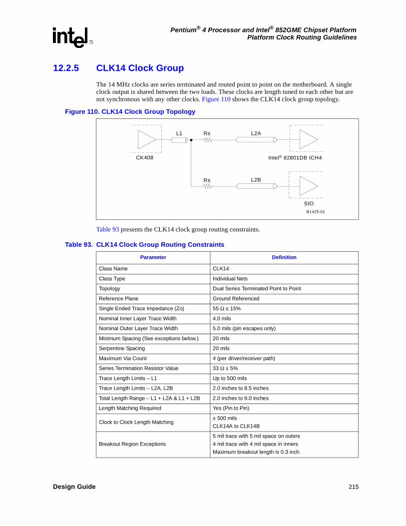
Design Guide 215
Pentium® 4 Processor and Intel® 852GME Chipset PlatformPlatform Clock Routing Guidelines
12.2.5 CLK14 Clock Group
The 14 MHz clocks are series terminated and routed point to point on the motherboard. A single clock output is shared between the two loads. These clocks are length tuned to each other but are not synchronous with any other clocks. Figure 110 shows the CLK14 clock group topology.
Table 93 presents the CLK14 clock group routing constraints.
Figure 110. CLK14 Clock Group Topology
B1425-01
CK408 Intel® 82801DB ICH4
L2A
Rs
RsL1
L2B
SIO
Table 93. CLK14 Clock Group Routing Constraints
Parameter Definition
Class Name CLK14
Class Type Individual Nets
Topology Dual Series Terminated Point to Point
Reference Plane Ground Referenced
Single Ended Trace Impedance (Zo) 55 Ω ± 15%
Nominal Inner Layer Trace Width 4.0 mils
Nominal Outer Layer Trace Width 5.0 mils (pin escapes only)
Minimum Spacing (See exceptions below.) 20 mils
Serpentine Spacing 20 mils
Maximum Via Count 4 (per driver/receiver path)
Series Termination Resistor Value 33 Ω ± 5%
Trace Length Limits – L1 Up to 500 mils
Trace Length Limits – L2A, L2B 2.0 inches to 8.5 inches
Total Length Range – L1 + L2A & L1 + L2B 2.0 inches to 9.0 inches
Length Matching Required Yes (Pin to Pin)
Clock to Clock Length Matching± 500 mils
CLK14A to CLK14B
Breakout Region Exceptions
5 mil trace with 5 mil space on outers
4 mil trace with 4 mil space in inners
Maximum breakout length is 0.3 inch.

216 Design Guide
Pentium® 4 Processor and Intel® 852GME Chipset PlatformPlatform Clock Routing Guidelines
12.2.6 DOTCLK Clock Group
The 48 MHz DOTCLK is series terminated and routed point to point on the motherboard. This clock operates independently and is not length tuned to any other clock. Figure 111 shows the DOTCLK clock topology.
Table 94 presents the DOTCLK clock routing constraints.
Figure 111. DOTCLK Clock Topology
B1426-01
CK408 GMCH
L2RsL1
Table 94. DOTCLK Clock Routing Constraints
Parameter Definition
Class Name DOTCLK
Class Type Individual Net
Topology Series Terminated Point to Point
Reference Plane Ground Referenced
Single Ended Trace Impedance (Zo) 55 Ω ± 15%
Nominal Inner Layer Trace Width 4.0 mils
Nominal Outer Layer Trace Width 5.0 mils (pin escapes only)
Minimum Spacing (See exceptions below.) 25 mils
Maximum Via Count 4
Series Termination Resistor Value 33 Ω ± 5%
Trace Length Limits – L1 Up to 500 mils
Trace Length Limits – L2 2.0 inches to 8.0 inches
Total Length Range – L1 + L2 2.0 inches to 8.5 inches
Length Matching Required No
Breakout Exceptions
5 mil trace with 5 mil space on outers
4 mil trace with 4 mil space in inners
Maximum breakout length is 0.3 inch.
NOTE: The DOTCLK is used internally by the GMCH to generate the pixel clock and must exhibit very low jitter. Take care to avoid routing through noisy areas and spacing rules should be observed. Guard traces may be employed if necessary with ground stake vias on no less than 0.5-inch intervals.

Design Guide 217
Pentium® 4 Processor and Intel® 852GME Chipset PlatformPlatform Clock Routing Guidelines
12.2.7 SSCCLK Clock Group
The 48/66 MHz SSCCLK operates independently and is not length tuned to any other clock. This clock employs a spread-spectrum device in its path to reduce EMI. The overall clock path is divided into two segments as shown below with each segment series terminated and routed point to point. Figure 112 shows the SSCCLK clock topology.
Table 95 presents the SSCCLK clock routing constraints.
Figure 112. SSCCLK Clock Topology
B 1 4 2 7 -0 1
C K 4 0 8
G M C H
L 2R sL 1
R s L 4L 3
S S C
Table 95. SSCCLK Clock Routing Constraints
Parameter Definition
Class Name SSCCLK
Class Type Individual Net
Topology Series Terminated Point to Point
Reference Plane Ground Referenced
Single Ended Trace Impedance (Zo) 55 Ω ± 15%
Nominal Inner Layer Trace Width 4.0 mils
Nominal Outer Layer Trace Width 5.0 mils (pin escapes only)
Minimum Spacing (See exceptions below.) 20 mils
Maximum Via Count 4 (per driver/receiver path)
Series Termination Resistor Value 33 Ω ± 5%
Trace Length Limits – L1 Up to 500 mils
Trace Length Limits – L2 1.0 inch to 4.0 inches
Trace Length Limits – L3 Up to 500 mils
Trace Length Limits – L4 1.0 inch to 7.0 inches
Total Length Range – L1 + L2 + L3 + L4 3.0 inches to 8.5 inches
Length Matching Required No
Breakout Exceptions
5 mil trace with 5 mil space on outers
4 mil trace with 4 mil space in inners
Maximum breakout length is 0.3 inch.

218 Design Guide
Pentium® 4 Processor and Intel® 852GME Chipset PlatformPlatform Clock Routing Guidelines
12.2.8 USBCLK Clock Group
The 48 MHz USBCLK is series terminated and routed point to point on the motherboard. This clock operates independently and is not length tuned to any other clock. Figure 113 shows the USBCLK clock topology.
Table 96 presents the USBCLK clock routing constraints.
Figure 113. USBCLK Clock Topology
B1426-01
CK408 GMCH
L2RsL1
Table 96. USBCLK Clock Routing Constraints
Parameter Definition
Class Name USBCLK
Class Type Individual Net
Topology Series Terminated Point to Point
Reference Plane Ground Referenced
Single Ended Trace Impedance (Zo) 55 Ω ± 15%
Nominal Inner Layer Trace Width 4.0 mils
Nominal Outer Layer Trace Width 5.0 mils (pin escapes only)
Minimum Spacing (See exceptions below.) 20 mils
Maximum Via Count 4
Series Termination Resistor Value 33 Ω ± 5%
Trace Length Limits – L1 Up to 500 mils
Trace Length Limits – L2 3.0 inches to 12.0 inches
Total Length Range – L1 + L2 3.0 inches to 12.5 inches
Length Matching Required No
Breakout Exceptions
5 mil trace with 5 mil space on outers
4 mil trace with 4 mil space in inners
Maximum breakout length is 0.3 inch.

Design Guide 219
Pentium® 4 Processor and Intel® 852GME Chipset PlatformPlatform Clock Routing Guidelines
12.3 CK-408 PWRDWN# Signal Connections
For systems that do not support S1M but do support the S3 state, the PWRDWN# input of the CK-408 clock chip should be connected to the SLP_S3# output of the ICH4. It is not recommended that PWRDWN# be pulled-up to the CK-408’s 3.3 V power supply if the S3 state is the second highest, power consuming state supported by the platform (that is, S1M and S2 not supported). The advantage of using SLP_S3# rather than the 3.3-V supply to qualify PWRDWN# is that it reduces the likelihood of the CK-408 clocks driving into unpowered components and potentially damaging the clock input buffers. SLP_S3# may help reduce power consumption because it is asserted before the 3.3 V supply is shut off, thus minimizing the amount of time that the clocks are left toggling.

This page intentionally left blank.
220 Design Guide
Pentium® 4 Processor and Intel® 852GME Chipset PlatformPlatform Clock Routing Guidelines

Design Guide 221
Pentium® 4 Processor and Intel® 852GME Chipset PlatformIntel® 852GME Chipset Platform Power Delivery Guidelines
Intel® 852GME Chipset Platform Power Delivery Guidelines 13
13.1 Definitions
Suspend-To-RAM (STR):
In the STR state, the system state is stored in main memory and all unnecessary system logic is turned off. Only main memory and logic required to wake the system remain powered.
Full-power operation:
During full-power operation, all components on the motherboard remain powered. Full-power operation includes both the full-on operating state and the S1 (PROCESSOR stop-grant) state.
Suspend operation:
During suspend operation; power is removed from some components on the motherboard. The customer reference board supports three suspend states: Suspend-to-RAM (S3), Suspend-to-Disk (S4), and Soft-off (S5).
Power rails:
An ATX power supply has six power rails: +5 V, -5 V, +12 V, -12 V, +3.3 V, 5 Vsb. In addition to these power rails, several other power rails are created with voltage regulators.
Core power rail:
Power rail that is only on during full-power operation. These power rails are on when the PSON signal is asserted to the ATX power supply. The core power rails that are distributed directly from the ATX 12 V power supply are +5 V, -5 V, +12 V, -12 V, +3.3 V.
Standby power rail:
A power rail that is on during suspend operation (these rails are also on during full-power operation). These rails are on at all times (when the power supply is plugged into AC power). The only standby power rail that is distributed directly from the ATX power supply is: 5 Vsb (5V Standby). There are other standby rails that are created with voltage regulators on the motherboard.
Derived power rail:
A derived power rail is any power rail that is generated from another power rail using an on-board voltage regulator. For example, 3.3 Vsb is usually derived (on the motherboard) from 5 Vsb using a voltage regulator.

222 Design Guide
Pentium® 4 Processor and Intel® 852GME Chipset PlatformIntel® 852GME Chipset Platform Power Delivery Guidelines
Dual power rail:
A dual power rail is derived from different rails at different times (depending on the power state of the system). Usually, a dual power rail is derived from a standby supply during suspend operation and derived from a core supply during full-power operation.
Note: The voltage on a dual power rail may be misleading.
13.2 Power Delivery Map
Figure 114 shows the power delivery architecture for an example Intel® 852GME chipset platform.
During STR, only the necessary devices are powered. These devices include: main memory, the ICH4 resume well, PCI wake devices (via 3.3 Vaux), AC’97, and USB. To ensure that enough power is available during STR, complete a thorough power budget. The power requirements should include each device’s power requirements, both in suspend and in full-power. Compare the power requirements with the power budget supplied by the power supply. Due to the requirements of main memory and the PCI 3.3 Vaux (and possibly other devices in the system), it is necessary to create dual power rails.
The solutions in this design guide are only examples. Many power distribution methods achieve the similar results. When deviating from these examples, it is critical to consider the effect of a change.

Design Guide 223
Pentium® 4 Processor and Intel® 852GME Chipset PlatformIntel® 852GME Chipset Platform Power Delivery Guidelines
Figure 114 shows the platform power delivery map.
Figure 114. Platform Power Delivery Map
VRM
1.5V VREG
3.3V 5V 5VSB 12V
ATX 12V Power Supply
2.5V VREG on S0/S1
1.8V VREG
MCH Core 1.5V
Processor Vtt
MCH DDR System Memory 2.5V MCH Hub Interface 1.8V
MCH AGP MCH Vtt
Processor Core
DDR System Memory 2.5V
Intel® 82801DB ICH4 Core 1.5V
ICH4 I/O 3.3V ICH4 Resume 1.5V
ICH4 Resume I/O 3.3V ICH4 RTC 3.3V
FWH 3.3V
LPC Super I/O 3.3V
CK-408 3.3V
1.5V VREG
ICH4 5V
Processor VID VID VREG
DDR Vtt 1.25V 1.25V VREG
2.5V VREG on S3
3.3V VREG
1.25V VREG on S0/S1/S3
ICH4 Hub Interface 1.8V
ICH4 5V Standby
ICH4 Vtt

224 Design Guide
Pentium® 4 Processor and Intel® 852GME Chipset PlatformIntel® 852GME Chipset Platform Power Delivery Guidelines
13.3 GMCH/Intel® 82801DB ICH4 Platform Power-Up Sequence
Figure 115 shows the power-on timing sequence for a GMCH/Intel® 82801DB ICH4-based platform.
Table 97 presents the timing sequence parameters for Figure 115.
Figure 115. GMCH/Intel® 82801DB ICH4 Platform Power-Up Sequence
VccSus
RunningSUSCLK
SLP_S3#
Vcc
PWROK, VGATE
SUS_STAT#
PCIRST#
FrequencyStraps
STPCLK#,CPUSLP#
Strap Values Normal Operation
Hub interface "CPUReset Complete"
message
RSMRST#,RSM_PWROK
T173
T176
T177
T178T181
T181
T182
T184
T185
T186
G3 S3 S0 S0 stateG3 S5System
State S4
SLP_S4#
SLP_S5# T183
T183a
T183b

Design Guide 225
Pentium® 4 Processor and Intel® 852GME Chipset PlatformIntel® 852GME Chipset Platform Power Delivery Guidelines
Table 97. Timing Sequence Parameters for Figure 115
Symbol Description Min Max Units Notes Fig
T173 VCCSus supplies active to RSMRST# inactive. 5 - ms Figure 115
T176 VCC supplies active to PWROK, VGATE active. 10 - ms Figure 115
T177PWROK and VGATE active and SYS_RESET# inactive to SUS_STAT# inactive.
32 38 RTCCLK Figure 115
T178 SUS_STAT# inactive to PCIRST# inactive. 1 3 RTCCLK Figure 115
T181 VCCSus active to SLP_S5#, SUS_STAT# and PCIRST# active. 50 ns Figure 115
T182/T183 RSMRST# inactive to SUSCLK running, SLP_S5# inactive. 110 ms 1 Figure 115
T183a SLP_S5# inactive to SLP_S4# inactive. 1 2 RTCCLK Figure 115
T183b SLP_S4# inactive to SLP_S3# inactive. 1 2 RTCCLK Figure 115
T184
VCC active to STPCLK#, CPUSLP#, STP_CPU#, STP_PCI#, SLP_S1#, C3_STAT# inactive, and CPU Frequency Strap signals high.
50 ns Figure 115
T185
PWROK and VGATE active and SYS_RESET# inactive to SUS_STAT# inactive and CPU Frequency Straps latched to strap values.
32 38 RTCCLK 2 Figure 115
T186CPU Reset Complete to Frequency Straps signals unlatched from strap values.
7 9 CLK66 3 Figure 115
NOTES:1. When there is no RTC battery in the system, so VCCRTC and the VCCSus supplies come up together, the
delay from RTCRST# and the RSMRST# inactive to SUSCLK toggling may be as much as 1000 ms.2. These transitions are clocked off the internal RTC. One RTC clock is approximately 32 µs.3. This transition is clocked off the 66 MHz CLK66. On4 CLK66 is approximately 15 ns.

226 Design Guide
Pentium® 4 Processor and Intel® 852GME Chipset PlatformIntel® 852GME Chipset Platform Power Delivery Guidelines
Table 98 shows the power on sequencing timing diagram (VR circuitry).
Table 99 presents the timing parameters for Figure 98.
13.3.1 ICH4 Power Sequencing Requirements
13.3.1.1 3.3/1.5 V Power Sequencing
The ICH4 has power sequencing requirements for the 3.3 V and 1.5 V rails in respect to each other. This requirement is as follows: The 1.5 V rail must power up before or simultaneously with the 3.3 V rail. The 3.3 V and 1.5 V rails must power down simultaneously.
The majority of the ICH4 I/O buffers are driven by the 3.3 V supplies but are controlled by logic powered by the 1.5 V supplies. Therefore, another consequence of faulty power sequencing arises when the 3.3 V supply comes up first. In this case, the I/O buffers may be in an undefined state until the 1.5 V logic is powered up. Some signals that are defined as ‘Input-only’ actually have output buffers that are normally disabled, and the Intel ICH4 may unexpectedly drive these signals when the 3.3 V supply is active while the 1.5 V supply is not.
Table 98. Power On Sequencing Timing Diagram (VR Circuitry)
BCLK
Vcc
PWRGOOD
RESET#
VCCVID
VID_GOOD
VID[4:0]
T9 T10
T7 T8
Table 99. Timing Sequence Parameters for Figure 116
Sym Description Min Max Units Notes Fig
T7 VCCVID > 1V to VID_GOOD high 1 us Figure 98
T8 VID_GOOD to VCC valid maximum time 50 ms Figure 98
T9 PWRGOOD inactive pulse width 10 BCLKS Figure 98
T10 PWRGOOD to RESET# deassertion time 1 ms Figure 98
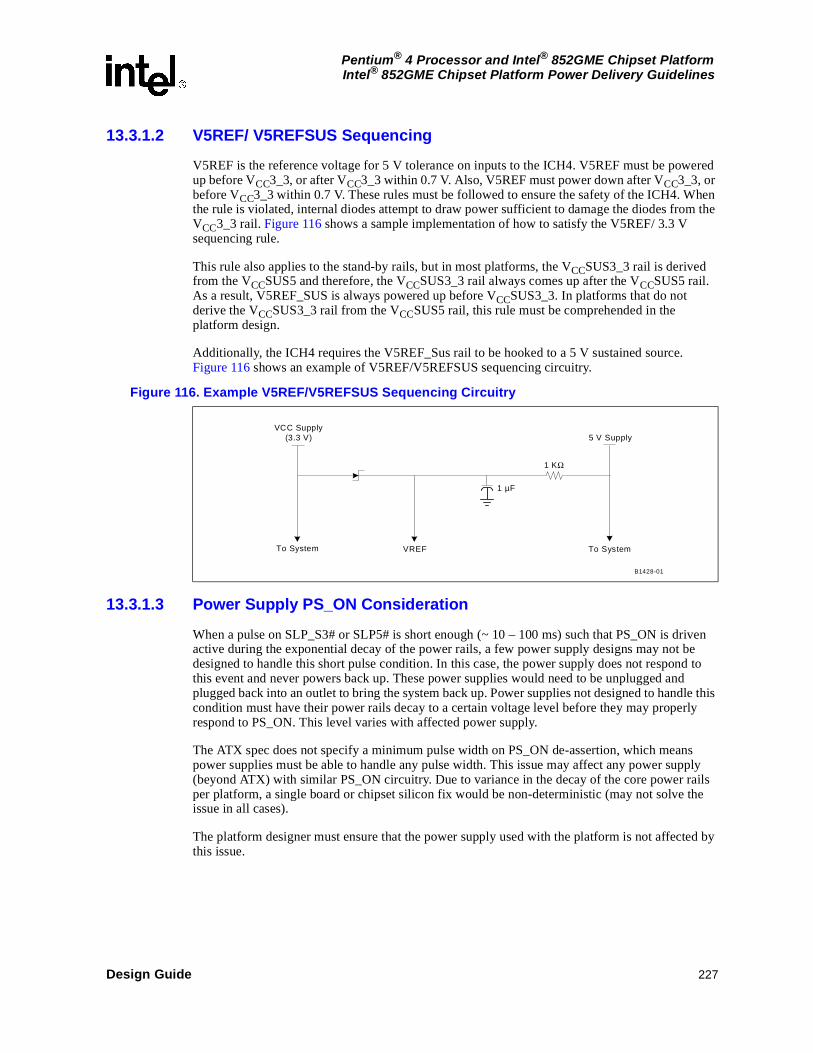
Design Guide 227
Pentium® 4 Processor and Intel® 852GME Chipset PlatformIntel® 852GME Chipset Platform Power Delivery Guidelines
13.3.1.2 V5REF/ V5REFSUS Sequencing
V5REF is the reference voltage for 5 V tolerance on inputs to the ICH4. V5REF must be powered up before VCC3_3, or after VCC3_3 within 0.7 V. Also, V5REF must power down after VCC3_3, or before VCC3_3 within 0.7 V. These rules must be followed to ensure the safety of the ICH4. When the rule is violated, internal diodes attempt to draw power sufficient to damage the diodes from the VCC3_3 rail. Figure 116 shows a sample implementation of how to satisfy the V5REF/ 3.3 V sequencing rule.
This rule also applies to the stand-by rails, but in most platforms, the VCCSUS3_3 rail is derived from the VCCSUS5 and therefore, the VCCSUS3_3 rail always comes up after the VCCSUS5 rail. As a result, V5REF_SUS is always powered up before VCCSUS3_3. In platforms that do not derive the VCCSUS3_3 rail from the VCCSUS5 rail, this rule must be comprehended in the platform design.
Additionally, the ICH4 requires the V5REF_Sus rail to be hooked to a 5 V sustained source. Figure 116 shows an example of V5REF/V5REFSUS sequencing circuitry.
13.3.1.3 Power Supply PS_ON Consideration
When a pulse on SLP_S3# or SLP5# is short enough (~ 10 – 100 ms) such that PS_ON is driven active during the exponential decay of the power rails, a few power supply designs may not be designed to handle this short pulse condition. In this case, the power supply does not respond to this event and never powers back up. These power supplies would need to be unplugged and plugged back into an outlet to bring the system back up. Power supplies not designed to handle this condition must have their power rails decay to a certain voltage level before they may properly respond to PS_ON. This level varies with affected power supply.
The ATX spec does not specify a minimum pulse width on PS_ON de-assertion, which means power supplies must be able to handle any pulse width. This issue may affect any power supply (beyond ATX) with similar PS_ON circuitry. Due to variance in the decay of the core power rails per platform, a single board or chipset silicon fix would be non-deterministic (may not solve the issue in all cases).
The platform designer must ensure that the power supply used with the platform is not affected by this issue.
Figure 116. Example V5REF/V5REFSUS Sequencing Circuitry
B1428-01
VCC Supply(3.3 V)
To System
5 V Supply
To SystemVREF
1 µF
1 KΩ

228 Design Guide
Pentium® 4 Processor and Intel® 852GME Chipset PlatformIntel® 852GME Chipset Platform Power Delivery Guidelines
13.3.2 GMCH Power Sequencing Requirements
No GMCH power sequencing requirements exist for the Intel® 82852GME GMCH platform. Verify that all GMCH power rails are stable before de-asserting reset, but the power rails may be brought up in any order desired. Good design practice would have all GMCH power rails come up as close in time as practical, with the core voltage coming up first.
The ICH4’s CPUPWRGOOD output represents the logical AND of its PWROK and VGATE inputs. When VGATE is asserted, it indicates that core power and the PCICLK are stable and PCIRST# will be de-asserted a minimum of 1 ms later. It is the responsibility of the system designers to ensure that the power and timing requirements for the processor and GMCH are met.
13.3.3 DDR Memory Power Sequencing Requirements
No DDR-SDRAM power sequencing requirements are specified during power up or power down if the following criteria are met:
• VDD and VDDQ are driven from a single power converter output.
• VTT is limited to 1.44 V (reflecting VDDQ(max)/2 + 50 mV VREF variation + 40 mV VTT variation)
• VREF tracks VDDQ/2
• A minimum resistance of 42 Ω (22 Ω series resistor + 22 Ω parallel resistor ± 5% tolerance) limits the input current from the VTT supply into any pin.
When the above criteria cannot be met by the system design, Table 100 must be adhered to during power up. Refer to Intel® DDR 200 JEDEC Spec Addendum for more details.
13.3.3.1 VTT Rail Power Down Sequencing During Suspend
The VTT termination voltage for the DDR bus must not be turned off until all populated rows of memory have been placed into power down mode through the deassertion of the SCKE signals. After all rows of memory are powered off, the VTT termination voltage may be removed. During entry into suspend and during suspend, VTT must not glitch. VTT must not be turned off until after the deassertion of the SCKE signals.
The voltage supplied to SMVREF, VREF, and SMRCOMP may also be removed once all rows of memory are powered off and SCKE must not glitch during entry into suspend and during suspend. Power to these pins must not be turned off until after the deassertion of the SCKE signals.
Table 100. DDR Power-Up Initialization Sequence
Voltage Description Sequencing Voltage Relationship to Avoid Latch-up
VDDQ After or with VDD < VDD + 0.3 V
VTT After or with VDDQ < VDDQ + 0.3 V
VREF After or with VDDQ < VDQ + 0.3 V

Design Guide 229
Pentium® 4 Processor and Intel® 852GME Chipset PlatformIntel® 852GME Chipset Platform Power Delivery Guidelines
13.3.3.2 VTT Rail Power Up Sequencing During Resume
During resume from the S3 state, the reverse sequencing of the power rails and control signals must occur to ensure a smooth exit from suspend. The VTT termination voltage must be supplied and steady before the system begins exit from suspend. VTT must not glitch during resume. SMVREF, VREF, and SMRCOMP also need to be supplied and valid before the assertion of the SCKE signals. These reference voltages and resistive compensation are necessary in order for the GMCH and the memory devices to recognize the valid assertion of SCKE. SCKE must not glitch during resume and must rise monotonically.
VTT and VREF to the DIMMs and SMVREF and SMRCOMP to the GMCH must all be up and stable before the deassertion of PCIRST#.
13.4 Intel® 852GME Chipset Platform Power Delivery Guidelines
Each component is capable of generating large current swings when switching between logic high and logic low. This condition could cause the component voltage rails to drop below specified limits. To avoid this type of situation, ensure that the appropriate amount of bulk capacitance is added in parallel to the voltage input pins. Intel recommends that the developer use the amount of decoupling capacitors specified in this document to ensure the component maintains stable supply voltages. Place the capacitors as close to the package as possible. Rotate caps that set over power planes so that the loop inductance is minimized (see Figure 117). The basic theory for minimizing loop inductance is to consider which voltage is on Layer 2 (power or ground) and spin the decoupling cap with the opposite voltage toward the BGA (Ball Grid Array). This greatly minimizes the total loop inductance. Intel recommends that for prototype board designs, the designer should include pads for extra power plane decoupling caps.
Figure 117 shows an example for minimizing loop inductance.
13.4.1 Pentium® 4 Processor Decoupling Guidelines
See Section 4.1.7, “Decoupling Requirements” on page 40 for details.
Figure 117. Example for Minimizing Loop Inductance
Layer 1
Layer 2
Layer 3
Layer 4
GND
4.5 mils nominal
48 mils nominal
BGA Ball
BGA Ball
BGA Substrate
PAD
Trace connecting Pad to Via
VIA
GND Ball
PWR Ball
Copper Plane Under BGA
Decouplin g Cap
PWR
Current Flow to Decoupling Cap
GND

230 Design Guide
Pentium® 4 Processor and Intel® 852GME Chipset PlatformIntel® 852GME Chipset Platform Power Delivery Guidelines
13.4.2 Intel® 82852GME GMCH Decoupling Guidelines
Bulk decoupling is based on the VR solution used on the CRB design. Table 101 presents the minimum GMCH decoupling requirements.
Table 101. Intel® 82852GME GMCH Decoupling Recommendations
Pin Name Configuration F Qty Type Notes
VCC Tie to VCC1_2S
0.1 µF
10 µF
150 µF
4
1
2
XR7, 0603, 16 V, 10%
XR5, 1206, 6.3 V, 20%
SPC, E, 6.3 V, 20%
1 X 0.1 µF with in 200mils
3 X 0.1 µF on bottom side
VTTLF Tie to VCCP
0.1 µF
10 µF
150 µF
2
1
1
XR7, 0603, 16 V, 10%
XR5, 1206, 6.3 V, 20%
SPC, E, 6.3 V, 20%
2 X 0.1 µF on bottom side
VTTHF Tie to Ground 0.1 µF 5 XR7, 0603, 16 V, 10%
VCCHL Tie to VCC1_5S0.1 µF
10 µF
2
1
XR7, 0603, 16 V, 10%
XR5, 1206, 6.3 V, 20%
1 X 0.1 µF with in 200 mils
1 X 0.1 µF on bottom side
VCCSM Tie to VCC2_50.1 µF
100 µF
11
2
XR7, 0603, 16 V, 10%
TANT, D, 10 V, 20%
10 X 0.1 µF with in 200 mils
1 X 0.1 µF on bottom side
VCCDVO Tie to VCC1_5S
0.1 µF
10 µF
150 µF
2
1
1
XR7, 0603, 16 V, 10%
XR5, 1206, 6.3 V, 20%
SPC, E, 6.3 V, 20%
1 X 0.1 µF with in 200 mils
1 X 0.1 µF on bottom side
VCCDLVDS Tie to VCC1_5S
0.1 µF
22 µF
47 µF
1
1
1
XR7, 0603, 16 V, 10%
TANT, B, 10 V, 20%
TANT, D, 10 V, 20%
1 X 0.1 µF with in 200 mils
VCCTXLVDS Tie to VCCSus2_5
0.1 µF
22 µf
47 µF
3
1
1
XR7, 0603, 16 V, 10%
TANT, B, 10 V, 20%
TANT, D, 10 V, 20%
1 X 0.1 µF with in 200 mils
2 X 0.1 µF on bottom side
VCCGPIO Tie to VCC3_3S 0.1 µF 1 XR7, 0603, 16 V, 10%
SMVREF 0.1 µF 1 XR7, 0603, 16 V, 10% 1 X 0.1 µF on bottom side
SMVSWINGL 0.1 µF 1 XR7, 0603, 16 V, 10%
SMVSWINGH 0.1 µF 1 XR7, 0603, 16 V, 10%
HDVREF220 pF
1 µF
3
3
XR7, 0603, 25 V, 10%
XR5, 0603, 6.3 V, 20%
HAVREF 0.1 µF 1 XR7, 0603, 16 V, 10%
HCCREF 0.1 µF 1 XR7, 0603, 16 V, 10%
HXVSWING 0.1 µF 1 XR7, 0603, 16 V, 10%

Design Guide 231
Pentium® 4 Processor and Intel® 852GME Chipset PlatformIntel® 852GME Chipset Platform Power Delivery Guidelines
13.4.3 GMCH VCCSM Decoupling
Every GMCH ground and VCCSM power ball in the system memory interface should have its own via. For the VCCSM pins of the GMCH, a minimum of eleven 0603 form factor 0.1 µF high frequency capacitors is required and must be placed within 150 mils of the GMCH package. Distribute the eleven capacitors evenly along the GMCH DDR system memory interface and they must be placed perpendicular to the GMCH with the power (2.5 V) side of the capacitors facing the GMCH. The trace from the power end of the capacitor should be as wide as possible and it must connect to a 2.5 V power ball on the outer row of balls on the GMCH. Each capacitor should have their 2.5 V via placed directly over and connected to a separate 2.5 V copper finger, and they should be as close to the capacitor pad as possible, within 25 mils. The ground end of the capacitors must connect to the ground flood and to the ground plane through a via. Place this via as close to the capacitor pad as possible, within 25 mils with as thick a trace as possible.
13.4.4 DDR SDRAM VDD Decoupling
Discontinuities in the DDR signal return paths occur when the signals transition between the motherboard and the DIMMs. To account for this ground to 2.5 V discontinuity, a minimum of nine 0603 form factor 0.1 µF high-frequency bypass capacitors are required between the DIMMs to help minimize any anticipated return path discontinuities that are created. Distribute the capacitors as evenly as possible between the two DIMMs.
• Connect the wide ground trace from each capacitor to a via that transitions to the ground plane. Place each ground via as close to the ground pad as possible.
• Connect the wide 2.5 V trace from each capacitor to a via that transitions to the 2.5 V copper flood. Place each via as close to the capacitor pad as possible. Connect each capacitor pad to the closet 2.5 V DIMM pin on either the first or second DIMM connector with a wide trace.
13.4.5 DDR VTT Decoupling Placement and Layout Guidelines
The VTT termination rail must be decoupled using high-speed bypass capacitors, one 0603 form factor, 0.1 µF capacitor and one 0603 form factor, 0.01 µF capacitor per four DDR signals. They must be placed more than 100 mils from the termination resistors.
• A VTT copper flood must be used. The decoupling capacitors must be spread out across the termination island so that all the parallel termination resistors are near high-frequency capacitors.
• Place each capacitor ground via as close to the capacitor pad as possible, within 25 mils with as thick a trace as possible.

232 Design Guide
Pentium® 4 Processor and Intel® 852GME Chipset PlatformIntel® 852GME Chipset Platform Power Delivery Guidelines
13.4.6 DDR Power Delivery Design Guidelines
The main focus of these GMCH guidelines is to minimize signal integrity problems and improve the power delivery to the GMCH system memory interface and the DDR memory DIMMs. This section discusses the DDR memory system voltage and current requirements as determined at publishing of this document. This document is not the original source for these guidelines. Figure 118 shows the implementation of 2.5 V, 1.25 V and SMVREF on the CRB only as an example. It is the responsibility of the system designer to ensure that the power requirements for the DDR and GMCH are met. Refer to the following documents for the latest details on voltage and current requirements found in this design guide.
• Double Data Rate (DDR) SDRAM Specification, JEDEC Standard, JESD79
• Intel DDR 20 JEDEC Spec Addendum, Rev 0.9 or later
Figure 118 shows the DDR power delivery block diagram.
13.4.6.1 2.5 V Power Delivery Guidelines
The 2.5 V power for the GMCH system memory interface and the DDR DIMMs is delivered around the DDR command, control, and clock signals. Special attention must be paid to the 2.5 V copper flooding to ensure proper GMCH and DIMM power delivery. This 2.5 V flood must extend from the GMCH 2.5 V power vias all the way to the 2.5 V DDR voltage regulator and its bulk capacitors. The 2.5 V DDR voltage regulator must connect to the 2.5 V flood with a minimum of six vias. The DIMM connector 2.5 V pins as well as the GMCH 2.5 V power vias must connect to the 2.5 V copper flood.
In the areas where the copper flooding necks down around the GMCH make sure to keep these neck down lengths as short as possible. The 2.5 V copper flooding under the DIMM connectors must encompass all the DIMM 2.5 V pins and must be solid except for the small areas where the clocks are routed within the DIMM pin field to their specified DIMM pins.
Figure 118. DDR Power Delivery Block Diagram
Note: SMV RE F and +V 1.25 m ay optionally be on the sw itch rail and turned off in either S 3 orS4. This is only a block diagram . It is the respons ibility of the system designer to ensure thatthe tim ing requirem ents for the DDR m em ory devices and GMCH are m et.
B1429-01
Switching Regulator
VoutV in
Sense Adj.
+V 5+ V 2.5
Switching Regulator
+
-
+V 5
V in V out
S ense A dj.+ V_1.25S
SMVRE F
10 KΩ
10 KΩ

Design Guide 233
Pentium® 4 Processor and Intel® 852GME Chipset PlatformIntel® 852GME Chipset Platform Power Delivery Guidelines
Maintain a minimum of 12 mil isolation spacing between the copper flooding and any signals on the same layer.
Table 102 shows the voltage and current specifications for each the GMCH and memory reference and termination voltages. For convenience, tolerances are given in both percent and volts, although validation should be done using the specifications exactly as they are written. When the spec states a tolerance in terms of volts (for example, VREF states ± 0.025 V), use that specific voltage tolerance, not a percentage of the measured value. Likewise, use percentages where stated.
As presented in the following tables, only the 2.5 V supply has an absolute specification. The 1.25 V supply for both VREF and VTT need to track the 2.5 V supply closely.
Table 102 presents the DDR SDRAM memory supply voltage and current specification.
Table 102. DDR SDRAM Memory Supply Voltage and Current Specification
Name VDD VDDQ VREF Description
Purpose Core Supply Voltage
I/O Supply Voltage
I/O Reference Supply Voltage
Specification Definition VDD VDDQ VREF = (Vdd/2)
± 0.050 V ((2.5 V ± 8%) / 2) ± 0.050 V
Voltage Nominal (V) 2.500 2.500 1.250
Tolerance (±%) 8.0% 8.0% 4.0%
Tolerance (±V) 0.200 0.200 0.050
Max Absolute Spec Value (V) 2.700 2.700 1.400 ((2.5 V + 8%) / 2) + 0.050 V
Min Absolute Spec Value (V) 2.300 2.300 1.100 ((2.5 V - 8%) / 2) - 0.050 V
MAX RELATIVE SPEC NA NA (measured Vdd/2)
+ 0.050 VCalculated from measured
VCCSM value.
MIN RELATIVE SPEC NA NA (measured Vdd/2)
- 0.050 VCalculated from measured
VCCSM value.
IDD (max) IDDQ (max) IREF (max)
Absolute Maximum Current Requirements (A)
5.000 0.920 0.001 (1 mA)

234 Design Guide
Pentium® 4 Processor and Intel® 852GME Chipset PlatformIntel® 852GME Chipset Platform Power Delivery Guidelines
Table 103 presents the GMCH system memory supply voltage and current specification.
Table 104 presents the termination voltage and current specifications.
Table 103. GMCH System Memory Supply Voltage and Current Specification
Name VCCSM SMVREF VTT = SMRCOMP Description
PurposeGMCH DDR
Supply Voltage (I/O)
GMCH Reference Supply Voltage
SMRCOMP Termination Supply
Voltage
Definition VCCSM SMVREF = (VCCSM/2) ± 2% VTT = (Vref) ± 0.040V (((2.5V ± 5%) / 2)
± 0.050V) ± 0.040V)
Voltage Nominal 2.500 V 1.250 V 1.250 V
Tolerance + 5.0% + 2.0% + 3.2%
Tolerance + 0.125 + 0.025 + 0.040
Max Absolute Spec Value 2.625 V 1.339 V 1.440 V (((2.5V + 5%) / 2)
+ 0.050V) + 0.040V)
Min Absolute Spec Value 2.375 V 1.164 V 1.060 V (((2.5 V-5%)/2) -0.050 V)
-0.040V)
Max Relative Spec NA (Measured VCCSM/
2) + 2%(Measured Vref) +
0.04VCalculated from measured VCCSM value.
Min Relative Spec NA (Measured VCCSM/
2) - 2%(Measured Vref) -
0.040VCalculated from measured VCCSM value.
IVCCSM (max) ISMVREF (max) ITTRC (max)
Absolute Maximum Current Requirements
1.900 A 0.00005A (50 µA) 0.040A (40 µA)
Table 104. Termination Voltage and Current Specifications
Name VTT Description
Purpose Termination Supply Voltage, Static
Definition Vtt = (Vref) ± 0.040V (((2.5 V ± 8%) / 2) ± 0.050V) ± 0.040V
Voltage Nominal (V) 1.250
Tolerance (+/-%) 3.2%
Tolerance (+/-V) 0.040
Max Absolute Spec Value (V) 1.440 (((2.5V + 8%) / 2) + 0.050V) + 0.040V
Min Absolute Spec Value (V) 1.060 (((2.5V - 8%) / 2) - 0.050V) - 0.040V
Max Relative Spec (Measured Vref) + 0.040V Calculated from measured VCCSM value.
Min Relative Spec (Measured Vref) - 0.040V Calculated from measured VCCSM value.
ITT (max)
Absolute Maximum Current Requirements (A) 2.400

Design Guide 235
Pentium® 4 Processor and Intel® 852GME Chipset PlatformIntel® 852GME Chipset Platform Power Delivery Guidelines
13.4.6.2 GMCH and DDR SMVREF Design Recommendations
There is one SMVREF pin on the GMCH that is used to set the reference voltage level for the DDR system memory signals (SMVREF). The voltage level that needs to be supplied to this pin must be equal to VCCSM/2. As shown in Figure 116, Intel recommends the use of an OpAmp buffer to generate SMVREF from the 2.5 V supply. This should be used as the VREF signals to both the DDR memory devices and the SMVREF signal to the GMCH.
13.4.6.3 DDR SMRCOMP Resistive Compensation
The GMCH requires a system memory compensation resistor, SMRCOMP, to adjust buffer characteristics to specific board and operation environment characteristics. Refer to Figure 119 for details on resistive compensation. The SMRCOMP signal should be routed with as wide a trace as possible. It should be a minimum of 12 mils wide and be isolated from other signals with a minimum of 10 mils spacing.
Figure 119 shows the GMCH SMRCOMP resistive compensation.
The GMCH’s system memory resistive compensation mechanism also requires the generation of reference voltages to the SMVSWINGL and SMVSWINGH pins. The schematic for SMVSWINGL and SMVSWINGH voltage generation is illustrated in Figure 120. Two resistive dividers with R1b = R2a = 150 Ω ± 1% and R1a = R2b = 604 Ω ± 1% generate the SMVSWINGL and SMVSWINGH voltages. SMVSWINGL and SMVSWINGH components should be placed within 0.5 inch of their respective pins and connected with a 15 mil wide trace. To avoid coupling with any other signals, maintain a minimum of 25 mils of separation to other signals.
Figure 119. GMCH SMRCOMP Resistive Compensation
B1430-01
+2.5 V
SMRCOMP
0.1 µF
60.4 Ω ± 1%
60.4 Ω ± 1%

236 Design Guide
Pentium® 4 Processor and Intel® 852GME Chipset PlatformIntel® 852GME Chipset Platform Power Delivery Guidelines
Figure 120 shows the GMCH system memory reference voltage generation circuit.
13.4.6.4 DDR VTT Termination
The recommended topology for DDR-SDRAM Data, Control, and Command signal groups requires that all these signals to be terminated to a 1.25 V source, VTT, at the end of the memory channel opposite the GMCH. It is recommended that this VTT be generated from the same source as used for VCCSM, and not be used for GMCH and DDR SMVREF. This is because SMVREF has a much tighter tolerance and VTT may vary more easily depending on signal states. A solid 1.25 V termination island should be used to for this purpose and be placed on the surface signal layer, just beyond the last DIMM connector and must be at least 50 mils wide. The data and command signals should be terminated using one resistor per signal. Resistor packs and ± 5% tolerant resistors are acceptable for this application. Only signals from the same DDR signal group may share a resistor pack. See Section 6 for system memory guidelines.
13.4.6.5 DDR SMRCOMP, SMVREF and VTT 1.25 V Supply Disablein S3/Suspend
Regardless of how these 1.25 V supplies for GMCH are generated, they may be disabled during the S3 suspend state to further save power on the platform. This is possible because the GMCH does not require a valid reference voltage nor does it require the enabling of resistive compensation during suspend. However, some DDR memory devices may require a valid reference voltage during suspend. It is the responsibility of the system designer to ensure that requirements of the DDR memory devices are met.
The 2.5 V VCCSM power pins of the GMCH and the VDD power pins of the DDR memory devices do need to be on in S3 state.
Figure 120. GMCH System Memory Reference Voltage Generation Circuit
R1a604 Ω +1%
R2a150 Ω +1%
+VCCSM
Intel®
82852GMEGMCH
SMVSWINGLSMVSWINGL SMVSWINGH
R1b
150Ω +1%
R2b604 Ω +1%
+VCCSM
SMVSWINGH
0.10.1 µF µF
B1385-01

Design Guide 237
Pentium® 4 Processor and Intel® 852GME Chipset PlatformIntel® 852GME Chipset Platform Power Delivery Guidelines
13.4.7 Other GMCH Reference Voltage and Analog Power Delivery
13.4.7.1 GMCH GTLVREF
For GMCH, the GTLREF generation circuit has been broken down into three separate voltage references: host data reference voltage (HDVREF[2:0]), host address reference voltage (HAVREF) and host common clock reference voltage (HCCVREF). Maximum length from pin to voltage divider for each reference voltage should be less than 0.5 inch. Intel recommends traces that are ten mil wide. GMCH VREF may be maintained as individual voltage dividers as shown in Figure 121, Figure 122, and Figure 123.
Figure 121 shows the GMCH HDVREF[2:0] reference voltage generation circuit.
Figure 122 shows the GMCH HAVREF reference voltage generation circuit.
Figure 121. GMCH HDVREF[2:0] Reference Voltage Generation Circuit
B1431-01
Intel® 852GMEChipset
HDVREF0
HDVREF1
HDVREF2C1
1 µFC2
0.1 µF
R2100 Ω± 1%
R149.9 Ω± 1%
+VC CP
K21
J21
J17
GMCH_HDVR EF
Figure 122. GMCH HAVREF Reference Voltage Generation Circuit
B1432-01
Intel® 852GMEChipset
HAVREF
C11 µF
C30.1 µF
R2100 Ω± 1%
R149.9 Ω± 1%
+VCCP
Y22GMCH_HAVREF

238 Design Guide
Pentium® 4 Processor and Intel® 852GME Chipset PlatformIntel® 852GME Chipset Platform Power Delivery Guidelines
Figure 123 shows the GMCH HCCVREF reference voltage generation circuit.
13.4.7.2 GMCH AGTL+ I/O Buffer Compensation
The HXRCOMP and HYRCOMP pins of the GMCH should each be pulled-down to ground with a 27.4 Ω ± 1% resistor (see Figure 124). The maximum trace length from pin to resistor should be less than 0.5 inch and should be 18 mils wide to achieve the Zo = 27.4 Ω target. Also, the routing for HRCOMP should be at least 25 mils away from any switching signal.
13.4.7.3 GMCH AGTL+ Reference Voltage
The GMCH’s AGTL+ I/O buffer resistive compensation mechanism also requires the generation of reference voltages to the HXSWING and HYSWING pins with a value of 1/3*VCCP. Implementations for HXSWING and HYSWING voltage generation are illustrated in Figure 125. Two resistive dividers with R1a = R1b = 301 Ω ± 1% and R2a = R2b = 150 Ω ± 1% generate the HXSWING and HYSWING voltages. C1a = C1b = 0.1 µF act as decoupling capacitors and connect HXSWING and HYSWING to VCC_CORE. HSWING components should be placed within 0.5 inch of their respective pins and connected with a 15 mil wide trace. To avoid coupling with any other signals, maintain a minimum of 25 mils of separation to other signals.
Figure 123. GMCH HCCVREF Reference Voltage Generation Circuit
B1433-02
Intel® 852GMEChipset
HCCVREF
C11 µF
C30.1 µF
R2100 Ω± 1%
R149.9 Ω± 1%
+VCCP
Y28GMCH_HCCVREF
Figure 124. GMCH HXRCOMP and HYRCOMP Resistive Compensation
B1434-01
HYRCOMPHXRCOMP
27.4 Ω ± 1% 27.4 Ω ± 1%

Design Guide 239
Pentium® 4 Processor and Intel® 852GME Chipset PlatformIntel® 852GME Chipset Platform Power Delivery Guidelines
Figure 125 shows the GMCH HXSWING and HYSWING reference voltage generation circuit.
13.4.7.4 GMCH Analog Power
Table 105 summarizes the eight analog circuits that require filtered supplies on the Intel 82852GME GMCH. The analog circuits are: VCCASM, VCCQSM, VCCAHPLL, VCCADPLLA, VCCADPLLB, VCCADAC, VCCAGPLL, and VCCALVDS.
VCCADAC, VCCAHPLL, VCCAGPLL, and VCCALVDS do not require an RLC filter but do require decoupling capacitors. Figure 126 shows an example analog supply filter.
Figure 125. GMCH HXSWING and HYSWING Reference Voltage Generation Circuit
B1435-01
Intel®
82852GMEGMCH
HYSWINGHXSWINGHYSWINGHXSWING
C1bC1a
+VCCP +VCCP
R1a301 Ω
R2a150 Ω
R1b301 Ω
R2b150 Ω
Figure 126. Example Analog Supply Filter
Low Pass Filtering
Noise
L
C BULK C HIGH
V CC Filtered V CC
*R DAMP
*R DA MP is not required for all filters

240 Design Guide
Pentium® 4 Processor and Intel® 852GME Chipset PlatformIntel® 852GME Chipset Platform Power Delivery Guidelines
Table 105 presents the analog supply filter requirements.
Table 105. Analog Supply Filter Requirements
Required 852GME
Chipset FiltersRDAMP
RDAMP Location L CBULK CHIGH
VCCASM None N/A 1210 1 µH DCRmax 0.169 Ωs 100 µF 0603 0.1 µF X5R
VCCQSM 1 Ω In series with capacitor
0805 0.68 µH DCRmax 0.80 Ωs 1206 4.7 µF X5R 0603 0.1 µF X5R
VCCAHPLL None N/A None None 0603 0.1 µF X5R
VCCADPLLA 1 Ω In series with inductor 0805 0.10 µH 220 µF 0603 0.1 µF X5R
VCCADPLLB 1 Ω In series with inductor 0805 0.10 µH 220 µF 0603 0.1 µF X5R
VCCADAC None N/A None None 0603 0.1 µF X5R0603 0.01 µF X5R
VCCAGPLL None N/A None None 0603 0.1 µF X5R
VCCALVDS None N/A None None 0603 0.1 µF X5R

Design Guide 241
Pentium® 4 Processor and Intel® 852GME Chipset PlatformIntel® 852GME Chipset Platform Power Delivery Guidelines
13.4.8 Intel® 82801DB ICH4 Decoupling/Power Delivery Guidelines
13.4.8.1 ICH4 Decoupling
The ICH4 is capable of generating large current swings when switching between logic high and logic low. This condition could cause the component voltage rails to drop below specified limits. To avoid this type of situation, ensure that the appropriate amount of decoupling capacitance is added in parallel to the voltage input pins. Intel recommends that the developer use the amount of high-frequency decoupling capacitors specified in table below to ensure that component maintains stable supply voltages. Low-frequency decoupling is dependent on layout and system power supply design. Table 106 presents the ICH4 decoupling requirements.
13.5 Clock Driver Power Delivery Guidelines
Special care must be taken to provide a quiet VDDA supply to the Ref VDD, VDDA, and the 48 MHz VDD. These VDDA signals are especially sensitive to switching noise induced by the other VDDs on the cock chip. They are also sensitive to switching noise generated elsewhere in the system such as the CPU VRM. Design the CLC pi-filter to provide the best reasonable isolation. Intel recommends that a solid ground plane be underneath the clock chip on Layer 2. (Assuming top trace is Layer 1.) Intel also recommends that a ground flood be placed directly under the clock chip to provide a low impedance connection for the VSS pins.
For ALL power connections to planes, decoupling capacitors and vias, use the MAXIMUM trace width allowable and shortest possible lengths to ensure lowest possible inductance. The decoupling capacitors should be connected as shown in Figure 127, taking care to connect the VDD pins directly to the VDD side of the capacitors. However, the VSS pins should not be connected directly to the VSS side of the capacitors. Instead, connect them to the ground flood under the part that is viaed to the ground plane. This is done to avoid VDD glitches propagating out and getting coupled through the decoupling capacitors to the VSS pins. This method has been shown to provide the best clock performance.
Table 106. Intel® 82801DB ICH4 Decoupling Requirements
Pin Decoupling Requirements
Decoupling Type (Ball type) Decoupling Placement
VCC3_3 (6) 0.1 µF Decoupling Cap (Vss) Place near balls: A4, A1, H1, T1, AC10, and AC18
VCCSUS3_3 (2) 0.1 µF Decoupling Cap (Vss) Place near balls: A22 and AC5
V_CPU_IO (1) 0.1 µF Decoupling Cap (Vcc) Place near ball: AA23
VCC1_5 (2) 0.1 µF Decoupling Cap (Vss) Place near balls: K23 and C23
VCCSUS1_5 (2) 0.1 µF Decoupling Cap (Vss) Place near balls: A16 and AC1
V5REF (1) 0.1 µF Decoupling Cap (Vcc) Place near ball: E7
V5_REF_SUS (1) 0.1 µF Decoupling Cap (Vss) Place near ball: A16
VCCRTC (1) 0.1 µF Decoupling Cap (Vcc) Place near ball: AB5
VCCHI (2) 0.1 µF Decoupling Cap (Vss) Place near balls: T23 and N23
VCCPLL(1) 0.1µF
(1) 0.01µFDecoupling Cap (Vcc) Place near ball: C22
NOTE: Place capacitors less than 100 mils from the package.

242 Design Guide
Pentium® 4 Processor and Intel® 852GME Chipset PlatformIntel® 852GME Chipset Platform Power Delivery Guidelines
The ground flood should be viaed through to the ground plane with no less than 12 to 16 vias under the part and ensure that it is well connected. For all power connections, use heavy duty and/or dual vias. It is imperative that the standard signal vias and small traces not be used for connecting decoupling capacitors and ground floods to the power and ground planes. Generate VDDA by using a CLC pi-filter. Connect this VDDA to the VDD side of the three capacitors that require it, using a significant trace on the top layer. Route this trace from the CLC pi-filter using a star topology.
13.5.1 CK-408 Clock Driver Decoupling
When connecting the decoupling caps, connect the VDD pins directly to the VDD side of the caps. However, the VSS pins should not be connected directly to the VSS side of the caps. Instead, they should be connected to the ground flood under the part that is via’ed to the ground plane. This is done to avoid VDD glitches propagating out and getting coupled through the decoupling caps to the VSS pins. This method has been shown to provide the best clock performance.
The decoupling requirements for a CK-408 compliant clock synthesizer are as follows:
• One 10 µF bulk decoupling cap in a 1206 package placed close to the VDD generation circuitry.
• Six 0.1 µF high frequency decoupling caps in a 0603 package placed close to the VDD pins on the CK-408.
• Three 0.1 µF high frequency decoupling caps in a 0603 package placed close to the VDDA pins on the CK-408.
• One 10 µF bulk decoupling cap in a 1206 package placed close to the VDDA generation circuitry.

Design Guide 243
Pentium® 4 Processor and Intel® 852GME Chipset PlatformIntel® 852GME Chipset Platform Power Delivery Guidelines
Figure 127 shows the placement and connectivity for decoupling capacitors.
Figure 127. Placement and Connectivity for Decoupling Capacitors
V d d
V d d
1
38 19
5 1
5 2
5 3
5 4
5 5
56
39 18
40
4 1 4 2
43
44
4 5
4 6
47 48
49
50
17
16
15
14
13
12
10
11
9
8
7
6
5
4 3
2
35
3 6 37
26
25
24
23
22
21
20
30
28
3 1
27
32
33
34
2 9
V d d
V d d
V d d
V d d 48 M H z
V ss 48 M H z
V ss
V s s
V d d
V ss
V s s
V s s
V s s Ire f
X T A L _ In
X T A L _O u t
P C IF 0
P C IF 2
P C IF 1
P C I 0
P C I 3
P C I 2
P C I 1
P C I 6
P C I 5
P C I 4
6 6B uff0 / 3 V 6 6_2
66 B u ff1 / 3 V 66 _3
6 6B uf f2 / 3V 6 6_4
6 6In / 3 V 66 _5
P W R D W N #
R E F 0
S 1
S 0
C P U _S to p #
C P U 0
C P U /0
C P U 1
C P U /1
C P U 2
C P U /2
M ult0
IR E F
S 2
U S B 48 M H z
D O T 4 8 M H z
3V 6 6_ 1 / V C H
P C I_ S to p #
3 V 66 _ 0
V ss G ro u nd
F lo od
V s s
V d d
S D A T A
S C L K V tt_ P w rgd #
V d d A
Vs s A
V ss
V ss
V ss
V ss
V ss
V d d
Vd d
V dd
V dd
V dd
V dd
C 1
C 2
V d dA
V ss
C 3
C 4
C 5
C 6
V dd A
V dd A
Vs s P la ne V ias

244 Design Guide
Pentium® 4 Processor and Intel® 852GME Chipset PlatformIntel® 852GME Chipset Platform Power Delivery Guidelines
13.5.2 Hub Interface Decoupling
See Section 9.4 for details.
13.5.3 FWH Decoupling
Place a 0.1 µF capacitor between the VCC supply pins and the VSS ground pins to decouplehigh-frequency noise, which may affect the programmability of the device. The value of thelow-frequency bulk decoupling capacitor is dependent on board layout and system power supply design.
13.5.4 General LAN Decoupling
• All VCC pins should be connected to the same power supply.
• All VSS pins should be connected to the same ground plane.
• Four to six decoupling capacitors, including two 4.7 µF capacitors are recommended
• Place decoupling as close as possible to power pins.
13.6 Thermal Design Power
The thermal design power is the estimated maximum possible expected power generated in a component by a realistic application. It is based on extrapolations in both hardware and software technology over the life of the product. It does not represent the expected power generated by a power virus. The thermal design power numbers for the Intel® 82852GME GMCH are presented in Table 107, and the thermal design power numbers for the ICH4 are presented in Table 108.
For more information on the ICH4 thermal design, refer to the Intel® I/O Controller Hub 4 (ICH4) Thermal Design Guidelines.
Table 107. Intel® 82852GME GMCH Component Thermal Design Power
Intel® 82852GME GMCH - Thermal Design Power Consumption Dissipation (estimated)
Intel 82852GME GMCH 5.7 W (maximum)
Table 108. Intel® 82801DB ICH4 Component Thermal Design Power
Intel® 82801DB ICH4 - Thermal Design Power Consumption Dissipation (estimated)
Intel 82801DB ICH4 2.0 W (maximum)

Design Guide 245
Pentium® 4 Processor and Intel® 852GME Chipset PlatformLayout Checklist
Layout Checklist 14
This checklist selectively highlights some of the design considerations that should be reviewed prior to manufacturing Pentium® 4 processor systems that implement the Intel® 852GME chipset. Items contained within the checklist attempt to address important connections to these devices and any critical supporting circuitry. This is not a complete list, and it does not ensure that a design will function properly. Refer to details in this document and the appended Customer Reference Board schematics for complete design recommendations. The recommendations and considerations in this guide are subject to change.
The following recommendations are a summary of the information presented in this design guide. They are based on the example 8-layer stackup detailed in Chapter 3. Deviation from the example stackup will require thorough signal integrity and timing simulations.

246 Design Guide
Pentium® 4 Processor and Intel® 852GME Chipset PlatformLayout Checklist
14.1 Processor Layout Checklist
Table 109 presents the processor layout checklist.
Table 109. Processor Layout Checklist (Sheet 1 of 4)
Checklist Items Recommendations Notes
Pentium 4 Processor Front Side Bus Interface Signals
A[31:3]#1
ADSTB[1:0]#2
HDSTBN[3:0]#3
HDSTBP[3:0]#4
DINV[3:0]#
HD[63:0]#5
REQ[4:0]#6
Trace impedance = 53 Ω ± 15%.
• Use strip-line routing, referencing ground planes above and below the signal layer.
• Route data strobes and data signals 4/12 with board trace length between 2.0 and 6.0 inches.
• Use GMCH die-pad to processor pin length for all length matching operations.
• Length match data strobes of the same group to within ± 100 mils of each other and to the average length of their associated data signal group.
• Route all data signals as groups, on the same layer, and balance within group ± 100 mils with respect to the associated strobes.
• Route address strobes 4/12 and address signals 4/8 with board trace length between 2.0 and 6.0 inches.
• Trace length match address strobes to ± 200 mils of average length of their associated address signals group.
• AGTL+ Source Synchronous Signals.
• Refer to Section 8.4.2 for more information.
ADS#
BNR#
BR0#
DBSY#
DRDY#
HIT#
HITM#
LOCK#
DPWR#
BPRI#
DEFER#
RS[2:0]#
TRDY#8
• Trace impedance = 53 Ω ± 15%.
• Use strip-line routing, referencing solid ground planes.
• Route traces using 4/8 mils spacing with board trace length between 2.0 and 6.0 inches.
• Trace length matching is not required for common clock signals.
• Package length compensation is necessary in determining minimum board trace length.
• AGTL+ Common Clock Signals.
• Refer to Section 8.4.3 for more information.

Design Guide 247
Pentium® 4 Processor and Intel® 852GME Chipset PlatformLayout Checklist
RESET#7
When ITP700 Is Not Used:• Trace impedance = 53 Ω ± 15%.
• Use strip-line routing, referencing solid ground planes.
• Route traces using 4/8 mils spacing with board trace length between 2.0 and 6.0 inches.
• Trace length matching is not required for common clock signals.
• Package length compensation is necessary in determining minimum board trace length.
• Refer to ITP Section of this layout checklist for treatment of RESET# signal when implementing ITP700FLEX debug port.
• AGTL+ Common Clock Signal.
• Refer to Section 8.4.3 for more information.
IERR#
• May be routed as a test point or to any optional system receiver.
• May be routed as strip-line or micro-strip with trace impedance = 53 Ω ± 15%.
• Place pull-up resistor Rpu within three inches of the Intel® 82801DB I/O Controller Hub 4 (ICH4).
• Pull-up voltage for termination resistor Rpu is VCC_CPU.
• Asynchronous AGTL+ Output Signal.
• Refer to Topology 1A in Section 8.4.4.1 for resistor values and trace length recommendations.
PROCHOT#
• May be routed as strip-line or micro-strip with trace impedance = 53 Ω ± 15%.
• Use recommended voltage translation logic for an appropriate system receiver.
• Pull-up voltage for termination resistor Rpu is VCC_CPU
• Asynchronous AGTL+ Output Signal.
• Refer to Topology 1B in Section 8.4.4.2 for resistor values and trace length recommendations.
FERR#
THERMTRIP#
• Connect FERR# to the processor and the ICH4.
• Recommend connecting processor signal THERMTRIP# to the ICH4, but may be connected to any optional system receiver, with consideration for any voltage level translation if necessary.
• May be routed as strip-line or micro-strip with trace impedance= 53 Ω ± 15%.
• Place pull-up resistor Rpu within three inches of ICH4.
• Pull-up voltage for termination resistor Rpu is VCC.
• Asynchronous AGTL+ Output Signals.
• Refer to Topology 1C in Section 8.4.4.3 for resistor values and trace length recommendations.
Table 109. Processor Layout Checklist (Sheet 2 of 4)
Checklist Items Recommendations Notes

248 Design Guide
Pentium® 4 Processor and Intel® 852GME Chipset PlatformLayout Checklist
PWRGOOD
• May be routed as strip-line or micro-strip with trace impedance= 53 Ω ± 15%.
• Route point-to-point between the ICH4 signal CPUPWRGD and CPU signal PWRGOOD, trace length range between 1.0 and 12 inches.
• Place a termination resistor Rpu within three inches of CPU pin. T-split routing should not be used.
• Pull-up voltage for termination resistor Rpu is VCC_CPU.
• Asynchronous Open Drain CMOS Input Signal.
• Refer to Topology 2C in Section 8.4.4.6 for resistor values and detailed routing recommendations.
IGNNE#
LINT0/INTR
LINT1/NMI
SMI#
SLP#
A20M#
STPCLK#
• May be routed as strip-line or micro-strip with trace impedance = 53 Ω ± 15%.
• Implement a point-to-point connection between the ICH4 and CPU, trace length range between 1.0 and 17 inches.
• No additional components are necessary for this topology.
• Asynchronous CMOS Input Signals.
• Refer to Topology 2B in Section 8.4.4.5.
INIT#
• May be routed as strip-line or micro-strip with trace impedance= 53 Ω ± 15%.
• Route signal point-to-point between the ICH4 and CPU, trace length range max 17 inches.
• Voltage level translation is required from the ICH4 INIT# pin to FWH.
• Asynchronous CMOS Input Signal.
• Refer to Topology 3 in Section 8.4.4.7 for resistor values and trace length recommendations.
• The Intel customer reference board makes use of an optional alternative circuit for FWH voltage translation. Refer to schematic appendix.
Other Signals
BCLK, BCLK#
CPU BCLK, BCLK# from CK-408 should be routed as differential pairs and length matched to the GMCH BCLK, BCLK# signals.
• Refer to host clock group routing guidelines detailed in Section 12.2.1.
• Refer to Chapter 12 for detailed breakdown of all system clock routing recommendations.
COMP[0,1] Terminate each signal to ground with 51 Ω ±1% resistors.
• Refer to Section 8.4.4.9 for detailed layout recommendations.
Processor Decoupling, VREF and Filtering
GTLREF
• Connect CPU GTLREF pin to a 49.9 kΩ ± 1% and 100 kΩ ± 1% resistive divider to VCC_CPU.
• No decoupling on this signal.
• Connect voltage divider node to CPU GTLREF pin with a Zo = 53 Ω trace that is shorter than 0.5 inch.
• Minimum separation from other switching signals should be 10 mils.
Refer to Section 8.2.1 for more information.
Table 109. Processor Layout Checklist (Sheet 3 of 4)
Checklist Items Recommendations Notes

Design Guide 249
Pentium® 4 Processor and Intel® 852GME Chipset PlatformLayout Checklist
VCC_CPU
Decoupling
Recommended bulk decoupling:• (10) 560µF AI POLYMER -
ESR 5 mΩ (typ) and ESL 4.0 nH, placed one each near the CPU and the GMCH packages.
• (40) 22µF X5R 0603 caps - ESR 3.5 mΩ (typ) and ESL 1.4 nH, placed on the secondary side within the CPU package outline.
• (4) 1200µF AL Electrolytic 16V 2.1 A ripple caps - ESR 22 mΩ andESL 30 nH
• (4) 1206 pkg 4.7µF - ESR 6 mΩ and ESL 1.1 nH
Refer to Section 4.1.7 for processor VCCP decoupling recommendations.
NOTES:1. A[31:3]# pins on the processor correspond to HA[31:3]# pins on the GMCH.2. ADSTB[1:0]# pins on the processor correspond to HADSTB[1:0]# pins on the GMCH.3. DSTBN[3:0]# pins on the processor correspond to HDSTBN[3:0]# pins on the GMCH.4. DSTBP[3:0]# pins on the processor correspond to HDSTBP[3:0]# pins on the GMCH.5. D[63:0]# pins on the processor correspond to HD[63:0]# pins on the GMCH.6. REQ[4:0]# pins on the processor correspond to HREQ[4:0]# pins on the GMCH.7. The RESET# pin on the processor corresponds to the CPURST# pin on the GMCH.8. The TRDY# pin on the processor corresponds to the HTRDY# pin on the GMCH.
Table 109. Processor Layout Checklist (Sheet 4 of 4)
Checklist Items Recommendations Notes

250 Design Guide
Pentium® 4 Processor and Intel® 852GME Chipset PlatformLayout Checklist
14.2 Intel® 852GME Chipset GMCH (82852GME) Layout Checklist
Table 110 presents the Intel® 852GME chipset GMCH layout checklist.
Table 110. Intel® 852GME Chipset GMCH Layout Checklist (Sheet 1 of 5)
Checklist Items Recommendations Comments
Host Interface Signals
ADS#BNR#BPRI#BREQ0#1
CPURST#2
DBSY#DEFER#HA[31:3]#3 HD[63:0]#4
HADSTB[1:0]#5
HDSTBN[3:0]#6
HDSTBP[3:0]#7
HIT#HITM#HLOCK#10
HREQ[4:0]#8
HTRDY#9
DRDY#RS[2:0]#DINV[3:0]#
Refer to the Processor section of this checklist.
DDR System Memory Interface
SCK[5:0]SCK[5:0]#
• Route as closely-coupled differential pairs, three clock pairs to each DIMM.
• Spacing to other DDR signals should not be less than 20 mils. Isolation from non-DDR signals should be 25 mils.
• Route on internal layers, except for pin escapes.
• Nominal internal trace width 7 mils and nominal internal spacing 4 mils.
• Routed trace length limits are 3.5 to 6.5 inches.
• Length match clock pairs to ±10 mils.
• Match all DIMM0 clock lengths and match all DIMM1 clock lengths.
• Use GMCH package lengths for pad-to-pin length tuning.
Refer to the detailed routing guidelines in Section 6.4.1.
SDQ[71:0]SDM[8:0]SDQS[8:0]
• Route SDQ/SDM with trace impedance 55 Ω ± 15% using 2:1 spacing.
• Route SDQS strobes similarly with 3:1 spacing.
• Isolation from non-DDR signals should be 20 mils.
• Overall min/max length to the DIMM must comply with clock length matching requirements.
Refer to the detailed routing guidelines in Section 6.4.4.

Design Guide 251
Pentium® 4 Processor and Intel® 852GME Chipset PlatformLayout Checklist
SCKE[3:0]SCS[3:0]#
• Route with trace impedance 55 Ω ± 15% using 2:1 spacing.
• Isolation from non-DDR signals should be 20 mils.
• GMCH pad to DIMM trace length limits are 2.0 to 6.0 inches.
• Place parallel termination resistor within 2.0 inches of DIMM pad.
• Overall min/max length to the DIMM must comply with clock length matching requirements.
Refer to the detailed routing guidelines in Section 6.4.5.
SRAS#SCAS#SWE#SMA[12:6,3,0]SBA[1:0]
• Route with trace impedance 55 Ω ± 15% using 2:1 spacing.
• Isolation from non-DDR signals should be 20 mils.
• GMCH pad to first DIMM trace length limits are 2.0 to 5.5 inches.
• Total DIMM to DIMM spacing should be less than two inches.
• Place parallel termination resistor within 1.5 inches of the second DIMM pad.
• Overall min/max length to the DIMM must comply with clock length matching requirements.
Refer to the detailed routing guidelines in Section 6.4.6.
SMA[5,4,2,1]SMAB[5,4,2,1]
• Route with trace impedance 55 Ω ± 15% using 2:1 spacing.
• Isolation from non-DDR signals should be 20 mils.
• GMCH pad to DIMM trace length limits are 2.0 to 6.0 inches.
• Place parallel termination resistor within 2.0 inches of the DIMM pad.
• Overall min/max length to the DIMM must comply with clock length matching requirements.
Refer to the detailed routing guidelines in Section 6.4.7.
RCVENIN#RCVENOUT#
• Internally shunted on Intel® 852GME chipset - no external connection necessary.
• Recommendation is that both signals be transitioned to the secondary side with vias next to the package balls to facilitate probing.
Refer to the detailed routing guidelines in Section 6.4.8.
Table 110. Intel® 852GME Chipset GMCH Layout Checklist (Sheet 2 of 5)
Checklist Items Recommendations Comments

252 Design Guide
Pentium® 4 Processor and Intel® 852GME Chipset PlatformLayout Checklist
DDR System Memory Decoupling
GMCH VCCSM Decoupling
• Requires a minimum of eleven 0603, 0.1µF caps placed within 150 mils of the GMCH package.
• Distribute evenly along the DDR memory interface, placed perpendicular to the GMCH with the power side of the caps facing the GMCH.
• Each GMCH ground and VCCSM power ball should have its own via.
• Each via should be as close to the associated cap pad as possible, within 25 mils and with as thick a trace as possible.
Refer to Section 13.4.3 for more information.
DDR Bypass Caps
• Place nine evenly spaced 0.1µF 0603 caps between the DIMMs.
• A wide trace from each cap should connect to a via that transitions to the ground plane layer.
• A wide trace should connect the 2.5 V side of each cap to a via that transitions to the 2.5 V plane, each via placed as close to the cap pad as possible.
• Each cap should also connect to the closest 2.5 V DIMM pin on either DIMM connector with a wide trace.
• Helps minimize return path discontinuities.
• Refer to Section 13.4.4 for more information.
DDR VTT Decoupling
• Decouple VTT termination rail using one 0603 0.1µF capacitor per two DDR signals.
• Spread out placement across the VTT termination rail, connecting directly to the rail, so that each parallel termination resistor is within 100 mils of one of these high-frequency capacitors.
• Each ground via should be as close to the associated cap pad as possible, within 25 mils and with as thick a trace as possible.
• Also, place one 4.7µF ceramic capacitor on each end of the termination island, and place one 4.7µF ceramic capacitor near the center of the termination island.
• Low frequency bulk decoupling requirements at the VTT termination rail should be met with (4) 470µF caps placed evenly across the VTT rail, including one cap at each end.
Refer to Section 13.4.5 for more information.
Table 110. Intel® 852GME Chipset GMCH Layout Checklist (Sheet 3 of 5)
Checklist Items Recommendations Comments

Design Guide 253
Pentium® 4 Processor and Intel® 852GME Chipset PlatformLayout Checklist
Hub Interface
General Guidelines
• Route hub interface data and strobes with trace impedance 55 Ω ± 15% using 2:1 spacing and VSS reference.
• Route hub interface strobe and its complement as a differential pair, length matched within ± 10 mils.
• Maximum length for both data and strobe signals is 6.0 inches.
• Hub interface data and strobe signals are routed on the same layer, transitioning together when a layer change is required.
• Keep layer changes to a minimum, using only two vias per net.
• Refer to Section 9.2.1 for detailed routing recommendations.
• The platform design guide example references routing guidelines for the 8-bit Hub Interface using enhanced (parallel) termination.
Clocks and Reset Signals
BCLKBCLK#
• The differential host clock pair should be length matched to ± 10 mils and to the processor BCLK/BCLK# pair within ± 20 mils overall (match L1 segments to ± 10 mils across all pairs).
• Route as strip-line traces 4/7 mils spacing (except as allowed for pin escapes).
• Total length range is 2.0 to 8.5 inches.
• Refer to host clock group routing guidelines detailed in Section 12.2.1.
• Refer to Chapter 12 for detailed breakdown of all system clock routing recommendations.
GCLKIN
• Place series resistor close to CK408, within 500 mils.
• Total trace length range is 4.0 to 9.0 inches.
• Minimum spacing 20 mils.
• Overall length of CLK66 is considered the reference length for all other clocks, except USBCLK and CLK14.
• The length of CLK66 traces should be matched within ± 100 mils and then used as the basis for defining the length of all other length matched clocks.
Refer to CLK66 clock group routing guidelines detailed in Section 12.2.2.
RSTIN# Connect to PCIRST# output of the Intel® 82801DB ICH4.
GMCH Decoupling, VREF, and Filtering
HLRCOMPHLVREFPSWING
• GMCH HLRCOMP signal should be strapped to 1.2 V via 27.4 Ω ± 1% HLRCOMP resistor with trace impedance 55 Ω ± 15%.
• HLVREF and PSWING voltage requirements must be set appropriately for proper hub interface operation. The case is similar for HIREF and HIVSWING signals on ICH4.
Refer to Section 9.3 for HI specific voltage requirements and several options for voltage divider circuits.
Table 110. Intel® 852GME Chipset GMCH Layout Checklist (Sheet 4 of 5)
Checklist Items Recommendations Comments

254 Design Guide
Pentium® 4 Processor and Intel® 852GME Chipset PlatformLayout Checklist
HXRCOMPHYRCOMP
• Each signal should be pulled to ground with a 27.4 Ω ± 1% resistor.
• Max trace length to the resistor should be less than 0.5 inches and should be 18 mils wide to achieve the characteristic impedance target of 27.4 Ω.
• Maintain 25 mil separation from any switching signals.
• This signal is used to calibrate the Host AGTL+ I/O buffers characteristics to specific board characteristics.
• Refer to Section 13.4.4 for more information.
HDVREF[2:0]HAVREFHCCVREF
• Max length from pin to voltage divider for each reference voltage should be less than 0.5 inch.
• 10 mil traces are recommended.
• To provide constant and clean power delivery to the data, address, and common clock signals of the host AGTL+ interface.
• Refer to Section 13.4.7.1 for recommended individual voltage divider circuits.
HXSWINGHYSWING
• Voltage divider components for each input should be placed within 0.5 inch of their respective pins.
• Use a 15 mil wide trace maintaining a minimum of 25 mils separation to other signals.
• The HXSWING and HYSWING inputs of GMCH are used to provide reference voltage for the compensation logic.
• Refer to Section 13.4.7.3 for more information.
Analog Power Filtering
There are eight analog circuits that require filtered supplies on the Intel® 852GME chipset.
Refer to Section 13.4.7.4 for detailed filter requirements.
NOTES:1. The BREQ0# pin on the GMCH corresponds to the BR0# pin on the processor. 2. The CPURST# pin on the GMCH corresponds to the RESET# pin on the processor.3. HA[35:3]# pins on the GMCH correspond to A[31:3]# pins on the processor.4. HD[63:0]# pins on the GMCH correspond to D[63:0]# pins on the processor.5. HADSTB[1:0]# pins on the GMCH correspond to ADSTB[1:0]# pins on the processor.6. HADSTBN[3:0]# pins on the GMCH correspond to DSTBN[3:0]# pins on the processor.7. HADSTBP[3:0]# pins on the GMCH correspond to DSTBP[3:0]# pins on the processor.8. HREQ[4:0]# pins on the GMCH correspond to REQ[4:0]# pins on the processor.9. The HTRDY# pin on the GMCH corresponds to the TRDY# pin on the processor.
10.The HLOCK# pin on the GMCH correspond to LOCK# pin on the processor.
Table 110. Intel® 852GME Chipset GMCH Layout Checklist (Sheet 5 of 5)
Checklist Items Recommendations Comments
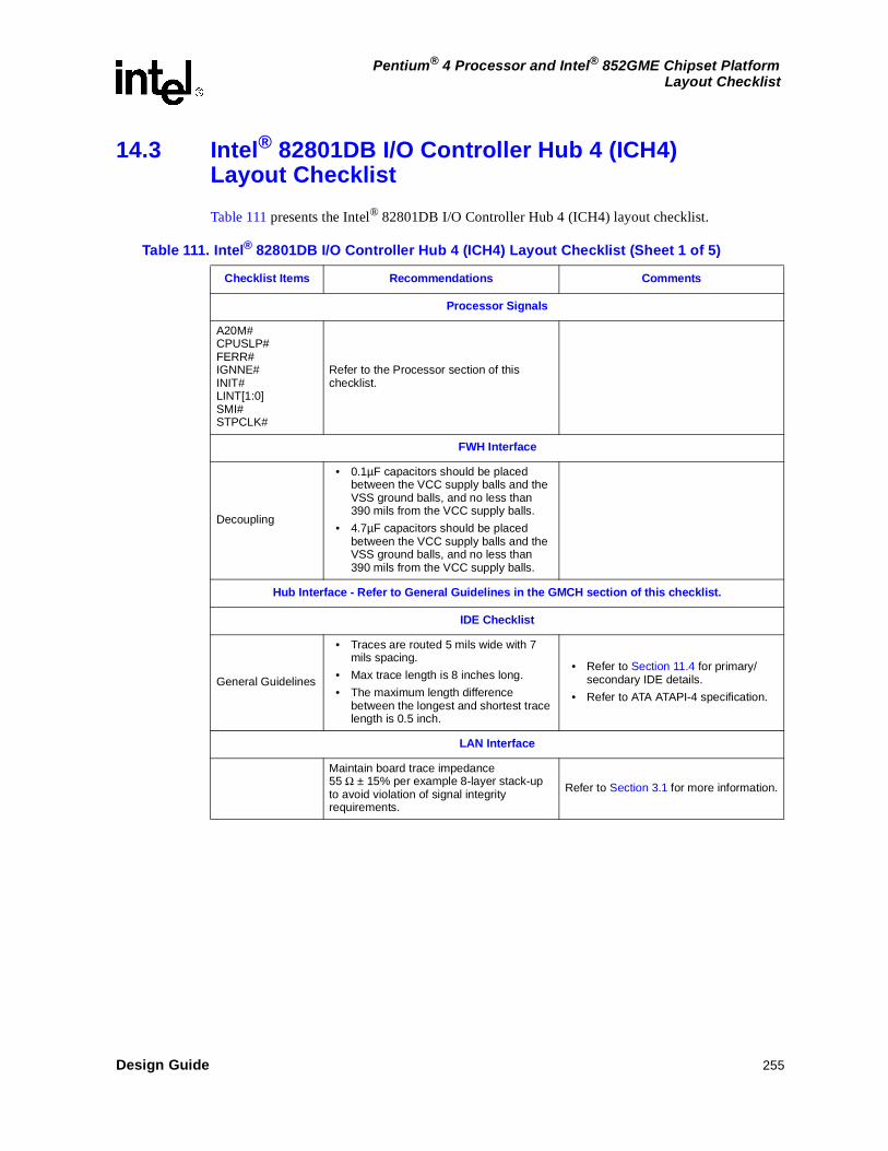
Design Guide 255
Pentium® 4 Processor and Intel® 852GME Chipset PlatformLayout Checklist
14.3 Intel® 82801DB I/O Controller Hub 4 (ICH4)Layout Checklist
Table 111 presents the Intel® 82801DB I/O Controller Hub 4 (ICH4) layout checklist.
Table 111. Intel® 82801DB I/O Controller Hub 4 (ICH4) Layout Checklist (Sheet 1 of 5)
Checklist Items Recommendations Comments
Processor Signals
A20M#CPUSLP# FERR#IGNNE#INIT#LINT[1:0]SMI#STPCLK#
Refer to the Processor section of this checklist.
FWH Interface
Decoupling
• 0.1µF capacitors should be placed between the VCC supply balls and the VSS ground balls, and no less than 390 mils from the VCC supply balls.
• 4.7µF capacitors should be placed between the VCC supply balls and the VSS ground balls, and no less than 390 mils from the VCC supply balls.
Hub Interface - Refer to General Guidelines in the GMCH section of this checklist.
IDE Checklist
General Guidelines
• Traces are routed 5 mils wide with 7 mils spacing.
• Max trace length is 8 inches long.
• The maximum length difference between the longest and shortest trace length is 0.5 inch.
• Refer to Section 11.4 for primary/secondary IDE details.
• Refer to ATA ATAPI-4 specification.
LAN Interface
Maintain board trace impedance 55 Ω ± 15% per example 8-layer stack-up to avoid violation of signal integrity requirements.
Refer to Section 3.1 for more information.

256 Design Guide
Pentium® 4 Processor and Intel® 852GME Chipset PlatformLayout Checklist
General Guidelines
Traces: 5 mils wide, 10 mils spacing. Refer to Section 11.14.1.1.
• Point-to-Point Single Solution - trace length range, ICH4 to Intel® 82562ET/ Intel® 82562EM Platform LAN Connect component should be 4.5 to 12 inches. Range for CNR is 2.0 to 9.5 inches.
• LOM and CNR Solution - trace length range ICH4 to RPAK should be L1 = 0.5 to 7.5 inches. Range for RPAK to PLC is L2 = 4 to (11.5 - L1) inches. Range for RPAK to CNR is L2 = 1.5 to (9.0 - L1) inches. CNR card trace length range is 0.5 to 3 inches. Total trace length is not to exceed 9.5 inches.
• To meet timing requirements.
• Refer to Section 11.14.1.1.1 for more information.
Stubs due to RPAK CNR/LOM stuffing option should not be present on the surface.
To minimize inductance.
All routing should reference VSS.
Maximum mismatch between the length of LAN_CLK and the length of any data trace is 0.5 inch (clock must be the longest trace).
To meet timing and signal quality requirements.
Table 111. Intel® 82801DB I/O Controller Hub 4 (ICH4) Layout Checklist (Sheet 2 of 5)
Checklist Items Recommendations Comments

Design Guide 257
Pentium® 4 Processor and Intel® 852GME Chipset PlatformLayout Checklist
General Guidelines
Maintain constant symmetry and spacing between the traces within a differential pair out of the LAN phy.
To meet timing and signal quality requirements.
Keep the total length of each differential pair under four inches.
Issues found with traces longer than four inches.
• IEEE phy conformance failures
• Excessive EMI and or degraded receive BER.
Do not route the transmit differential traces closer than 100 mils to the receive differential traces.
To minimize crosstalk.
Distance between differential traces and any other signal line must be at least 100 mils. (300 mils is recommended.)
To minimize crosstalk.
Route 5 mils on 7 mils for differential pairs (out of LAN phy).
To meet timing and signal quality requirements.
Differential trace impedance should be controlled to be ~100 Ω.
To meet timing and signal quality requirements.
For high-speed signals, the number of corners and vias should be kept to a minimum. When a 90-degree bend is required, use two 45-degree bends.
To meet timing and signal quality requirements.
Traces should be routed away from board edges by a distance greater than the trace height above the ground plane.
This allows the field around the trace to couple more easily to the ground plane rather than to adjacent wires or boards.
Do not route traces and vias under crystals or oscillators.
This prevents coupling to or from the clock.
Trace width to height ratio above the ground plane should be between 1:1 and 3:1.
To control trace EMI radiation.
Traces between decoupling and I/O filter capacitors should be as short and wide as practical.
Long and thin lines are more inductive and would reduce the intended effect of decoupling capacitors.
Vias to decoupling capacitors should be sufficiently large in diameter. To decrease series inductance.
Isolate I/O signals from high speed signals. To minimize crosstalk.
Avoid routing high-speed LAN or Phone line traces near other high-frequency signals associated with a video controller, cache controller, processor, or other similar device.
To minimize crosstalk.
Place the Intel® 82562ET/ Intel® 82562EM Platform LAN Connect component more than 1.5 inches away from any board edge.
This minimizes the potential for EMI radiation problems.
Table 111. Intel® 82801DB I/O Controller Hub 4 (ICH4) Layout Checklist (Sheet 3 of 5)
Checklist Items Recommendations Comments

258 Design Guide
Pentium® 4 Processor and Intel® 852GME Chipset PlatformLayout Checklist
General Guidelines
Place at least one bulk capacitor(4.7µF or greater OK) on each side of the Intel® 82562ET/ Intel® 82562EM Platform LAN Connect component.
Research and development has shown that this is a robust design recommendation.
Place decoupling capacitors (0.1µF) as close to the Intel 82562ET/ Intel 82562EM Platform LAN Connect component as possible.
ICH4 Power Decoupling
V_CPU_IO[2:0]Use one 0.1µF and one 1µF decoupling capacitor. Locate within 100 mils of the ICH4 package near ball AA23.
Refer to Section 13.4.8.1 for more information.
VCC3_3
Requires six 0.1µF decoupling capacitors. Place caps within 100 mils of the ICH4 package near balls A4, A1, H1, T1, AC10, and AC18.
VCCSUS3_3Requires two 0.1µF decoupling capacitors. Place within 100 mils of the ICH4 package near balls A22 and AC5.
VCC1_5Requires two 0.1µF decoupling capacitors. Place within 100 mils of the ICH4 package near balls K23 and C23.
VCCSUS1_5Requires two 0.1µF decoupling capacitors. Place within 100 mils of the ICH4 package near balls A16 and AC1.
V5REF_SUS
Requires one 0.1µF decoupling capacitor. V5REF_SUS affects only 5 V tolerance for USB OC[5:0]# balls, and may be connected to VCCSUS3_3 when 5 V tolerance on these signal is not required.
V5REF
Requires one 0.1µF decoupling capacitor placed near ball E7. V5REF is the reference voltage for 5 V tolerant inputs in the ICH4. Tie to balls V5REF[2:1]. V5REF must power up before or simultaneous to VCC3_3. It must power down after or simultaneous to VCC3_3.
VCCRTC Requires one 0.1µF decoupling capacitor placed near ball AB5.
VCCHI Requires two 0.1µF decoupling capacitors placed near balls T23 and N23.
VCCPLL Requires one 0.1µF and one 0.01µF decoupling capacitor placed near ball C22.
Table 111. Intel® 82801DB I/O Controller Hub 4 (ICH4) Layout Checklist (Sheet 4 of 5)
Checklist Items Recommendations Comments

Design Guide 259
Pentium® 4 Processor and Intel® 852GME Chipset PlatformLayout Checklist
RTC
General Guidelines
• RTC ball to crystal termination trace length should be less than one inch.
• Use 5 mil trace width (results in approximately 2 pF per inch).
• Minimize capacitance between RTCX1 and RTCX2.
• Put ground plane underneath crystal components.
• Do not route switching signals under the external components (unless on other side of board).
Refer to Section 11.13.1 for more information.
USB
General Guidelines
• Route all traces over continuous planes (ground) with no interruptions. Avoid crossing over anti-etch when possible. Crossing over anti-etch (plane splits) increases inductance and radiation levels by forcing a greater loop area. Likewise, avoid changing layers with high-speed traces. (Applies to USB signals, high-speed clocks, as well as slower signals that might be coupling to them.)
• Keep traces at least 50 mils away from the edge of the reference ground plane. This helps prevent the coupling of the signal onto adjacent wires, and helps prevent free radiation of the signal from the edge of the PCB.
• Maintain parallelism between USB differential signals with the trace spacing needed to achieve 90 Ω differential impedance. Recommended: Use of impedance calculator to determine the trace width and spacing required for the specific board stack-up being used. Using 4 mil traces with 4.5 mil spacing results in approximately 90 Ω differential trace impedance.
• Minimize the length of high-speed clock and periodic signal traces that run parallel to USB signal lines to minimize crosstalk. The minimum recommended spacing to clock signals is 50 mils.
• Use 20 mils minimum spacing between USB signal pairs and other signal traces. This helps to prevent crosstalk.
• USB signal pair traces should be trace length matched. Max trace length mismatch between USB signal pairs should be no greater than 150 mils.
• No termination resistors needed for USB.
Refer to Section 11.8.1 for detailed USB guidelines.
Refer to Section 11.8.1.4 for termination recommendations.
Table 111. Intel® 82801DB I/O Controller Hub 4 (ICH4) Layout Checklist (Sheet 5 of 5)
Checklist Items Recommendations Comments

This page intentionally left blank.
260 Design Guide
Pentium® 4 Processor and Intel® 852GME Chipset PlatformLayout Checklist

Design Guide 261
Pentium® 4 Processor and Intel® 852GME Chipset PlatformSchematic Checklist Summary
Schematic Checklist Summary 15
This checklist provides design recommendations and guidelines for Intel® 852GME chipset platform for use with the Pentium® 4 processor with 533 MHz system bus. This checklist highlights design considerations that should be reviewed prior to manufacturing a motherboard that implements the 852GME chipset. The items contained in this checklist attempt to address important connections to these devices and critical supporting circuitry.
This is not a complete list, and it does not ensure that a design will function properly. Beyond the items contained in the checklist, refer to items listed in the respective sections in this document.
Note: Unless otherwise specified, the default tolerance on resistors is ± 5%.

262 Design Guide
Pentium® 4 Processor and Intel® 852GME Chipset PlatformSchematic Checklist Summary
15.1 Pentium® 4 Processor Checklists
15.1.1 Resistor Recommendations Checklist
Table 112 presents the resistor recommendations checklist.
Table 112. Resistor Recommendations Checklist (Sheet 1 of 5)
Pin Name System Pull-up/Pull-down
Series Termination
Voltage Translation Notes √
A[31:3]# Connect to HA[31:3]# pins on MCH.
A[35:32]# No connect.
A20M#Point-to-point connection to Intel® 82801DB ICH4.
ADS#Connect to the associated pin on the MCH.
1
ADSTB[1:0]#Connect to HADSTB[1:0]# pins on MCH.
AP[1:0]# No connect.
BCLK[1:0]
Connect a 49.9 Ω ± 1% shunt source termination (Rt) resistor to GND for each signal on the processor side of the series resistor.
Connect 20-33 Ω series resistors to each clock signal.
Connect to CK_408.
BINIT# No Connect.
BNR#Connect to the associated pin on the MCH.
BPM[5:0]#
These signals should be terminated with a 51 Ω ± 5% resistor to VCC_CPU near the processor.
If a debug port is implemented termination is required near the debug port as well. Refer to the ITP700 Debug Port Design Guide for further information.
BPRI#Connect to the associated pin on the MCH.
BR0# 220 Ω ± 5% pull-up to VCC
Point-to-point connection to GMCH, with resistor placed by GMCH.
BSEL[0]Terminate to CK_408 3.3 V supply through a 1 kΩ resistor.
Connect to CK_408.
NOTE: Default tolerance for resistors is ± 5% unless otherwise specified.

Design Guide 263
Pentium® 4 Processor and Intel® 852GME Chipset PlatformSchematic Checklist Summary
COMP[1:0]Terminate to GND through a 51.1 Ω ± 1% resistor.
Minimize the distance from termination resistor and processor pin.
D[63:0]# Connect to HD[63:0]# pins on MCH.
DBI[3:0]#Connect to the associated pin on the MCH.
DBR#
Refer to the ITP700 Debug Port Design Guide for further information.
DBSY#Connect to the associated pin on the MCH.
DEFER#Connect to the associated pin on the MCH.
DP[3:0]# No connect.
DRDY#Connect to the associated pin on the MCH.
DSTBN[3:0]#Connect to HDSTBN[3:0]# pins on MCH.
DSTBP[3:0]#Connect to HDSTBP[3:0]# pins on MCH.
FERR# 62 Ω ± 5% pull-up to VCC
Point-to-point connection to Intel® 82801DB ICH4, with resistor placed by ICH4.
GTLREF[3:0]
Terminate to VCC_CPU through a 49.9 Ω ± 1% resistor. Terminate to GND through a 100 Ω ± 1% resistor. Should be 2/3 VCC_CPU.
Voltage divider should be placed within 1.5 inches of the processor pin. Place 1µF cap by the resistor divider, 220 pF by the processor pin. Minimum one GTLREF pin require to be connected as recommended above.
HIT#Connect to the associated pin on the MCH.
HITM#Connect to the associated pin on the MCH.
Table 112. Resistor Recommendations Checklist (Sheet 2 of 5)
Pin Name System Pull-up/Pull-down
Series Termination
Voltage Translation Notes √
NOTE: Default tolerance for resistors is ± 5% unless otherwise specified.

264 Design Guide
Pentium® 4 Processor and Intel® 852GME Chipset PlatformSchematic Checklist Summary
IERR# 62 Ω ± 5% pull-up to VCC
IERR# may also be routed to a test point or to any optional system receiver.
IGNNE#Point-to-point connection to Intel® 82801DB ICH4.
INIT# See Figure 128
Point-to-point connection to ICH4. Voltage transition circuit is required if connecting to FWH.
See Figure 128 for more information.
ITP_CLK0
Refer to the ITP700 Debug Port Design Guide for further information.
ITP_CLK1
Refer to the ITP700 Debug Port Design Guide for further information.
LINT0/INTR Point-to-point connection to ICH4.
LINT1/NMI Point-to-point connection to ICH4.
LOCK# Connect to HLOCK# pin on MCH.
MCERR# No Connect.
PROCHOT# 62 Ω ± 5% pull up to VCC
Refer to CRB schematic and Figure 130 for more details. When PROCHOT# is routed to external logic, voltage translation may be required. The receiver at the output of the voltage translation circuit may be any receiver that functions properly with the PROCHOT# signal.
PWRGOOD 300 Ω ± 5% pull-up to VCC
Point-to-point connection to Intel® 82801DB ICH4, with resistor placed by the processor.
REQ[4:0]#Connect to HREQ[4:0]# pins on MCH.
Table 112. Resistor Recommendations Checklist (Sheet 3 of 5)
Pin Name System Pull-up/Pull-down
Series Termination
Voltage Translation Notes √
NOTE: Default tolerance for resistors is ± 5% unless otherwise specified.

Design Guide 265
Pentium® 4 Processor and Intel® 852GME Chipset PlatformSchematic Checklist Summary
RESET# 51 Ω ± 5% pull-up to VCC.
Point-to-point connection to GMCH.
RS[2:0]#Connect to the associated pin on the MCH.
RSP# No connect.
SKTOCC#Connect to Glue Chip / Discrete Logic (if pin is used).
SLP# Point-to-point connection to ICH4.
SMI# Point-to-point connection to ICH4.
STPCLK# Point-to-point connection to ICH4.
TCK
Refer to the ITP700 Debug Port Design Guide for further information.
TDI
Refer to the ITP700 Debug Port Design Guide for further information.
TDO
Refer to the ITP700 Debug Port Design Guide for further information.
TESTHI[1:0],
TESTHI[5:2]
TESTHI[10:8]
TESTHI[12:11]
Matched resistors pull up to VCC with value ± 20% of trace impedance.
TESTHI pins may use individual pull-up resistors too.
THERMDAIf used, connect to thermal monitor circuitry.
THERMDCIf used, connect to thermal monitor circuitry.
THERMTRIP# 62 Ω ± 5% pull-up to VCC.
Point-to-point connection to Intel® 82801DB ICH4, with resistor placed by ICH4. If connecting to other device, voltage translation logic may be required.
TMS
Refer to the ITP700 Debug Port Design Guide for further information.
Table 112. Resistor Recommendations Checklist (Sheet 4 of 5)
Pin Name System Pull-up/Pull-down
Series Termination
Voltage Translation Notes √
NOTE: Default tolerance for resistors is ± 5% unless otherwise specified.

266 Design Guide
Pentium® 4 Processor and Intel® 852GME Chipset PlatformSchematic Checklist Summary
TRDY# Connect to HTRDY# pin on MCH.
TRST#
Refer to the ITP700 Debug Port Design Guide for further information.
VCC[85:0] Connect to VCC.
VCCA, VSSA, VCCIOPLL Connect to VCC via filter.
C1 = 22µF - 33µF with a 20% tolerance. The ESL is < 2.5 nH and the ESR < 0.225 Ω.
L1, L2 = 10µH ± 25%. Rdc = 0.4 ± 30%.
See Figure 129 for more information.
VCCSENSE, VSSSENSE
If used, connect to VR control silicon.
VCCVID Connect to 1.2 V linear regulator.
VID[4:0]
These signals must be pulled up to 3.3 V through either 1 kΩ pull-ups on the motherboard or with internal pull-ups in the VR or VRM.
Connect to VR or VRM.
VSS[182:0] Connect to GND.
Figure 128. Routing Illustration for INIT#
Table 112. Resistor Recommendations Checklist (Sheet 5 of 5)
Pin Name System Pull-up/Pull-down
Series Termination
Voltage Translation Notes √
NOTE: Default tolerance for resistors is ± 5% unless otherwise specified.
INIT# to FWH
4.7 k Ω
4.7 k Ω
INIT# from Intel® 82801DB ICH4
12 V
INIT# Routing

Design Guide 267
Pentium® 4 Processor and Intel® 852GME Chipset PlatformSchematic Checklist Summary
15.1.2 In Target Probe (ITP) Checklist
Table 113 presents the In Target Probe Checklist.
Figure 129. VCCIOPLL, VCCA, and VSSA Power Distribution
Figure 130. Voltage Translation Circuit for PROCHOT#
Processor Voltage
Translator External
Logic
L2 = 10"
L1 L3
VCC_CPU
Rpu
Pro_Therm_Routi
Table 113. In Target Probe (ITP) Checklist
Pin Name SystemPull-up /Pull-down
Series Termination Resistor (Ω) Notes √
BPM[5:0]# 51 Ω pull-up to VCC Connect to processor, with resistors placed by the processor.
DBR# 150-240 Ω pull-up to V3ALWAYS
If using ITP on interposer card, then DBR# should also be connected to DBRESET pin at the processor.
RESET# 51 Ω pull-up to VCC
If USING ITP700FLEX150 Ω from pull-up to ITP700FLEX See notes in Section 15.1.
FBO Connect to TCK pin of processor.
NOTE: The above recommendation is only for ITP700FLEX. If using other ITP, refer to the appropriate ITP documents

268 Design Guide
Pentium® 4 Processor and Intel® 852GME Chipset PlatformSchematic Checklist Summary
15.1.3 Decoupling Recommendations Checklist
Table 114 presents the decoupling recommendations checklist.
15.2 CK-408 Clock Checklist
15.2.1 Resistor Recommendations Checklist
Table 115 presents the CK-408 resistor recommendations checklist.
TCK 27.4 Ω ± 1% pull-down to gnd
Connect to processor, with resistor placed by ITP.
TDI 150 Ω pull-up to VCC Connect to processor, with resistor placed by Processor.
TDO 75 Ω pull-up to VCCConnect to processor, with resistor placed by ITP. If ITP not used, this signal may be left as NC.
TMS 39.2 Ω ± 1% pull-up to VCC
Connect to processor, with resistor placed by ITP.
TRST# 680 Ω pull-down to gnd Connect to processor.
VTAP, VTT[1:0] Connect to VCC One 0.1 µF decoupling cap is
required.
Table 113. In Target Probe (ITP) Checklist
Pin Name SystemPull-up /Pull-down
Series Termination Resistor (Ω) Notes √
NOTE: The above recommendation is only for ITP700FLEX. If using other ITP, refer to the appropriate ITP documents
Table 114. Decoupling Recommendations Checklist
Signal Configuration Value Qty Notes √
VCC[Vcc_core] Connect to VCC
560µF
22µF
1200µF
4.7µF
10
40
4
4
22µF caps in X5R, 1206 package for high frequency decoupling.
NOTE: Decoupling guidelines are recommendations based on our reference board design. Customers will need to take layout & PCB board design into consideration when deciding on overall decoupling solution.

Design Guide 269
Pentium® 4 Processor and Intel® 852GME Chipset PlatformSchematic Checklist Summary
Table 115. CK-408 Resistor Recommendations Checklist (Sheet 1 of 2)
Pin Name SystemPull-up/Pull-down
Series Resistor Notes √
3V66[0]
3V66[1]33 Ω
If the signal is used, one 33 Ω series resistor is required. If the signal is NOT used, it should be left as NC (Not Connected) or connected to a test point.
Two possible topologies for 3V66_1:
• Use directly for GMCH’s DREFSSCLK
• Use as input to an SSC device with SSC output to GMCH’s DREFSSCLK.
3V66_[4:2] 33 Ω
• The Intel CRB routes 3V66[2] (pin 21) to GCLKIN on GMCH.
• The other two signals route to ICH4 (CLK66) and AGP connector (AGPCLK)
CPU[0], CPU[0]# CPU[1], CPU[1]# CPU[2], CPU[2]#
49.9 Ω ± 1% pull-down to gnd 33 Ω
Use one pair for the processor and another pair for GMCH. If on-board ITP is implemented, the third pair of clock signals is used for the ITP connector. Otherwise, it may be routed to the dedicated ITP clock pins on the processor socket.
DOT_48 MHz 33 Ω Connect to GMCH’s DREFCLK.
IREF 475 Ω ± 1% pull-down to gnd Adjusts IREF to 2.32 mA
MULT[0] 10 KΩ pull-up to Vcc3_3CLK
PCI[6:0] 33 Ω Connect to various PCI devices.
PCIF[2], PCIF[1], PCIF[0] 33 Ω
Use one clock for Intel® 82801DB ICH4. Unused clock pins should be left as NC or connected to a test point.
PWRDWN#Terminate to VCC3_CLK through 1 kΩ resistor
Intel’s CRB does not support S1M.
REF0 33 Ω
This is the 14.318 MHz clock reference signal for ICH4, SIO and LPC. Each receiver requires one 33 Ω series resistor.
SEL[2]1 kΩ - 20 kΩ pull-down to GND. CRB uses 1 kΩ.
Configured for 133 MHz host clock, unbuffered mode, 0.710 mV swing.
SEL[1:0] Intel CRB uses 1 kΩ pull up to VCC3_CLK
Configured for 133 MHz host clock, unbuffered mode, 0.710 mV swing
USB_48MHz 33 Ω Connect to ICH4’s 48 MHz clock input.

270 Design Guide
Pentium® 4 Processor and Intel® 852GME Chipset PlatformSchematic Checklist Summary
XTAL_IN, XTAL_OUT
Terminate each pin to GND through a10 pF ± 5% capacitor
Connect to a 14.318 MHz crystal, placed within 500 mils of CK-408.
VDD[7:0], VDDA Connect to Vcc3_3 Refer to clock vendor datasheet for decoupling info.
VSS[5:0], VSSA Connect to GND
VSSIREF Connect to GND
Table 115. CK-408 Resistor Recommendations Checklist (Sheet 2 of 2)
Pin Name SystemPull-up/Pull-down
Series Resistor Notes √

Design Guide 271
Pentium® 4 Processor and Intel® 852GME Chipset PlatformSchematic Checklist Summary
15.3 Intel® 852GME Chipset GMCH Checklists
15.3.1 System Memory
15.3.1.1 GMCH System Memory Interface Checklist
Table 116 presents the GMCH system memory interface checklist.
Table 116. GMCH System Memory Interface Checklist (Sheet 1 of 2)
Pin Name SystemPull-up/Pull-down
Series Resistor Notes √
SRCVENIN# This signal should be routed to a via next to ball and left as a NC (No Connect).
SRCVENOUT# This signal should be routed to via next to ball and left as a NC (No Connect).
SBA[1:0], SCAS#,
SRAS#, SWE#56 Ω pull-up to Vcc1_25 10 Ω Connect to DIMM0 and DIMM1.
SCKE[1:0], SCS#[1:0] 56 Ω pull-up to Vcc1_25 Connect to DIMM 0
SCKE[3:2], SCS#[3:2] 56 Ω pull-up to Vcc1_25 Connect to DIMM1
SDQ[63:0], SDM[7:0], SDQS[7:0]
56 Ω pull-up to Vcc1_25 10 Ω
SDQ[71:64], SDM8, SDQS8 56 Ω pull-up to Vcc1_25 10 Ω
For Intel® 852GME chipset, if ECC support is not implemented, SDQ[71:64], SDM8, and SDQS8 should be left as NC. For ECC support, these signals connect to DIMMs.
SMA[12:6,3,0] 56 Ω pull-up to Vcc1_25 Connect to DIMM0 and DIMM1.
SMA[5,4,2,1]
SMAB[5,4,2,1]56 Ω pull-up to Vcc1_25 Use SMA[5,4,2,1] for DIMM0; use
SMAB[5,4,2,1] for the DIMM1.
SCK0, SCK0# SCK1, SCK1# SCK2, SCK2#
These clock signals connect differentially to DIMM 0.
Note: Refer Section 6 for GMCH Clock routing flexibility.
SCK3, SCK3# SCK4, SCK4# SCK5, SCK5#
These clock signals connect to DIMM 1.
SMVREF_0
Resistor Divider to V_2P5_SM consists of two identical resistors (50 Ω -150 Ω ± 1%)
Intel CRB uses 49.9 Ω.
Signal voltage level = V_2P5_SM/2. A buffer is used to provide the necessary current and reference voltage to SMVREF. Place a 0.1µF cap by GMCH, DIMM0 and DIMM1 pins.
SMVSWINGL604 Ω 1% pull-up to V_2P5_SM150 Ω 1% pull-down to gnd
Signal voltage level = 1/5 * V_2P5_SM.
Need 0.1µF cap at GMCH pin.
SMVSWINGH150 Ω 1% pull-up to V_2P5_SM604 Ω 1% pull-down to gnd
Signal voltage level = 4/5 * V_2P5_SM.
Need 0.1µF cap at GMCH pin.

272 Design Guide
Pentium® 4 Processor and Intel® 852GME Chipset PlatformSchematic Checklist Summary
Figure 131 shows the reference voltage level SMVREF.
SMRCOMP60.4 Ω 1% pull-up to V_2P5_SM60.4 Ω 1% pull-down to gnd
Signal voltage level = 1/2 * V_2P5_SM
Need 0.1µF cap by the voltage divider.
Table 116. GMCH System Memory Interface Checklist (Sheet 2 of 2)
Pin Name SystemPull-up/Pull-down
Series Resistor Notes √
Figure 131. Reference Voltage Level for SMVREF
+
-
V_2P5_SM
50Ω+/- 1%
50 Ω+/-1 %
SMVREF
GMCH
SMVREF_0
0.1 uF

Design Guide 273
Pentium® 4 Processor and Intel® 852GME Chipset PlatformSchematic Checklist Summary
15.3.1.2 DDR DIMM Interface Checklist
Table 117 presents the DDR DIMM interface checklist.
15.3.1.3 DIMM Decoupling Recommendation Checklist
Table 118 presents the DIMM decoupling recommendation checklist.
Table 117. DDR DIMM Interface Checklist
Pin Name Configuration Notes √
VREF[pin 1] Signal voltage level = V_2P5_SM / 2. Place a 0.1 pF cap by GMCH, DIMM0 and DIMM1
VDD[9:1] Connect to V_2P5_SM. Power must be provided during S3.
VDDSPD Connect to V-2P5_CORE.
VDDQ[16:1] Connect to V_2P5_SM.
SA[2:1] Connect to GND. These lines are used for strapping the SPD address for each DIMM.
SA0DIMM 0: Connect to GND.
DIMM 1: Connect to V_2P5_SM.
VSS[22:1] Connect to GND.
RESET(DU) Signal may be left as NC (Not Connected).
SDA/SCLConnect to Intel® 82801DB ICH4 SMBUS and SMLINK through isolation circuitry.
VDDID Signal may be left as NC (Not Connected).
DU[4:1] Signal may be left as NC (Not Connected).
GND[1:0] Signal may be left as NC (Not Connected).
A13, CS[3:2]#, BA2, WP, FETEN Signal may be left as NC (Not Connected).
NC [4:1] Signal may be left as NC (Not Connected).
Table 118. DIMM Decoupling Recommendation Checklist
Pin Name F Qty Notes √
V_1P25_MEMVTT
0.1µF
4.7µF
470µF
55
3
4
Place one 0.1µF cap close to every two pull up resistors terminated to V_1P25_MEMVTT (VTT for DDR signal termination. Place two 4.7µF caps at either end of the VTT island and one near the center. Four 470µF caps may be placed as bulk decoupling
V_2P5_SM
0.1µF
220µF
100µF
15
3
1
A minimum of nine high frequency caps are recommended to be placed between the DIMMS. A minimum of four low frequency caps are required.

274 Design Guide
Pentium® 4 Processor and Intel® 852GME Chipset PlatformSchematic Checklist Summary
15.3.2 Front Side Bus (FSB) Checklist
Table 119 presents the Front Side Bus (FSB) checklist.
Table 119. Front Side Bus (FSB) Checklist
Pin Name SystemPull-up/Pull-down
Notes √
CPURST# 51 Ω ± 1% pull up to VCCP. 150 Ω ± 1% series to ITP Connect to processor and ITP (if implemented).
HXSWING, HYSWING
301 Ω 1% pull-up to VCCP
150 Ω 1% pull-down to GND
Signal voltage level = 1/3 of VCCP.
• C1a = 0.1µF
• C1b=0.1µF
Trace should be 10-mil wide with 20-mil spacing.
See Figure 132 for more information.
HXRCOMP, HYRCOMP 27.4 Ω 1% pull down to GND One pulled-down resistor per pin. Trace should
be 10-mil wide with 20-mil spacing.
HDVREF[2:0]49.9 Ω 1% pull-up to VCC
100 Ω 1% pull-down to GNDSignal voltage level = 2/3 of VCC. Need one 0.1µF cap and one 1µF cap for voltage divider.
HAVREF49.9 Ω 1% pull-up to VCC
100 Ω 1% pull-down to GNDSignal voltage level = 2/3 of VCC. Need one 0.1µF cap and one 1µF cap for voltage divider.
HCCVREF49.9 Ω 1% pull-up to VCC
100 Ω 1% pull-down to GNDSignal voltage level = 2/3 of VCC. Need one 0.1µF cap and one 1µF cap for voltage divider.
Figure 132. Intel® 852GME Chipset HXSWING and HYSWING Reference Voltage Generation Circuit
B1594-01
GMCH
HYSWINGHXSWINGHYSWINGHXSWING
C1bC1a
+VCC +VCC
301 Ω± 1 %
150 Ω± 1%
301 Ω± 1 %
150 Ω± 1%

Design Guide 275
Pentium® 4 Processor and Intel® 852GME Chipset PlatformSchematic Checklist Summary
15.3.3 Hub Interface Checklist
Table 120 presents the Hub Interface checklist.
15.4 Graphics Interfaces Checklists
15.4.1 Low Voltage Differential Signaling (LVDS) Checklist
Table 121 presents the LVDS checklist.
Table 120. Hub Interface Checklist
Pin Name SystemPull-up/Pull-down
Notes √
HI[10:0] Connect to Intel® 82801DB ICH4.
HLSTB (S) Connect to ICH4.
HLSTB# (F) Connect to ICH4.
HLVREF See Section 9.4 for more information. Signal voltage level = 0.35 V ± 8%.
PSWING See Section 9.4 for more information.
Signal voltage level = 2/3 of V1P2_GMCH or 0.8 V ± 8%.
HLRCOMP 48.7 Ω ± 1% pull-up to V1P5_GMCH
Table 121. LVDS Checklist
Pin Name SystemPull-up/Pull-down
Notes √
LIBG 1.5 kΩ 1% pull-down to GND
IYAP[3:0]/IYAM[3:0]
IYBP[3:0]/IYBM[3:0]
If any of these LVDS data pairs are unused, they may be left as “no connect.”
ICLKAP/ICLKAM
ICLKBP/ICLKBMIf any of these LVDS clock pairs are not used, they may be left as “no connect.”
DDCPCLK,DDCPDATA
2.2 kΩ to 10 kΩ pull up to 3.3V if not used
LVDS Panel DDC Clock/Data pair to collect digital display EDID information.
PANELVDDEN 100 kΩ pull down Used for LVDS Panel Power Control.
PANELBKLTEN 100 kΩ pull down Used for LVDS Panel Backlight Enable.
PANELBKLTCTL 100 kΩ pull down Used for LVDS Panel Backlight Brightness Control.

276 Design Guide
Pentium® 4 Processor and Intel® 852GME Chipset PlatformSchematic Checklist Summary
15.4.2 Accelerated Graphics Port/ Digital Video Out (AGP /DVO) Checklist
Table 122 presents the AGP/DVO Checklist.
Table 122. AGP/DVO Checklist (Sheet 1 of 2)
Pin Name System Pull-up/Pull-down
Notes √
DVORCOMP 40.2 Ω ± 1% pull-down to gnd Trace should be 10-mil wide with 20-mil spacing.
GVREF
1 kΩ ± 1% pull-up to V_1P5_CORE
1 kΩ ± 1% pull-down to gnd
Signal voltage level = 1/2 of V_1P5_CORE. Need 0.1µF cap at GMCH pin and near ADD slot pin (if implemented).
GAD[28:25]/DVOCD[11:6]
GCBE#3/DVOCD5
GAD[23:19]/DVOCD[4:0]
GADSTB1/DVOCCLK
GADSTB#/DVOCCLK#
GAD17/DVOCHSYNC
GAD16/DVOCVSYNC
GAD18/DVOCBLANK#
If unused, these signals may be left as NC.
GAD31/DVOCFLDSTL 100 kΩ pull-down to gndPull-down resistor required only if signal is unused (10 kΩ - 100 kΩ). It is up to DVO device to drive this signal.
GAD30/DVOBCINTR# 100 kΩ pull-up to V_1P5_CORE
Pull-up resistor required only if signal is unused (10 kΩ - 100 kΩ). It is up to the DVO device to drive this signal.
GAD13/DVOBCCLKINT 100 kΩ pull-down to gnd
Pull-down resistor required only if signal is unused (10 kΩ - 100 kΩ). It is up to the DVO device to drive this signal.

Design Guide 277
Pentium® 4 Processor and Intel® 852GME Chipset PlatformSchematic Checklist Summary
GAD3/DVOBD0
GAD2/DVOBD1
GAD5/DVOBD2
GAD4/DVOBD3
GAD7/DVOBD4
GAD6/DVOBD5
GAD8/DVOBD6
GCBE#0/DVOBD7
GAD10/DVOBD8
GAD9/DVOBD9
GAD12/DVOBD10
GAD11/DVOBD11
GADSTB0/DVOBCLK
GADSTB#0/DVOBCLK#
GAD0/DVOBHSYNC
GAD1/DVOBVSYNC
GBCE#1/DVOBBLANK#
If AGP is not used these should left as NC.
GAD30/DVOBFLDSTL (pin M2)
100 kΩ pull-down to GND
For Intel® 852GME chipset, pull-down resistor required on this signal (10 kΩ - 100 kΩ).
GIRDY/MI2CCLK, GDEVSEL/MI2CDATA 2.2 kΩ pull-up to Vcc1_5
Pull-up resistor required on each signal even if they are unused (2.2 kΩ - 100 kΩ). This signal is 1.5 V tolerant. It may require voltage translation circuit.
GTRDY/MDVICLK, GFRAME#/MDVIDATA 2.2 kΩ pull-up to Vcc1_5
Pull-up resistor required on each signal even if they are unused (2.2 kΩ -100kΩ). This signal is 1.5 V tolerant. It may require voltage translation circuit.
GSTOP#/MDDCCLK, GAD15/MDDCDATA 2.2 kΩ pull-up to Vcc1_5
Pull-up resistor required on each signal even if they are unused (2.2 kΩ - 100 kΩ). This signal is 1.5 V tolerant. It may require voltage translation circuit.
GSBA[6:0]/ADDID[6:0] Leave as NC.
GSBA7/ADDID7 1 kΩ pull-down to GND if DVO device is onboard
If DVO interface is not used, this signal may be left as “no connect”. Otherwise, pull-down is needed.
GPAR/DVODETECT 1 kΩ pull-up to Vcc1_5 if DVO interface is unused
If DVO interface is used, leave as NC. This signal has internal pull-down.
GPIPE#/DPMS
If AGP is not used, connect this signal to 1.5 V version of the Intel® 82801DB ICH4 SUSCLK or a clock that runs during S1.
See Figure 133 for more information.
Table 122. AGP/DVO Checklist (Sheet 2 of 2)
Pin Name System Pull-up/Pull-down
Notes √

278 Design Guide
Pentium® 4 Processor and Intel® 852GME Chipset PlatformSchematic Checklist Summary
Figure 133. DPMS Clock Implementation
B1601-01
To GMCH DPMS pinPM_SUS_CLK
SUS_CLK
1 kΩ
Vcc1_5
Intel®82801DB
ICH4
1
2
BSS138SUS_CLK

Design Guide 279
Pentium® 4 Processor and Intel® 852GME Chipset PlatformSchematic Checklist Summary
15.4.3 Digital-to-Analog Converter (DAC) Checklist
Table 123 presents the DAC checklist.
Table 123. DAC Checklist
Pin Name SystemPull-up /Pull-down
In Series Notes √
REFSET 127 Ω 1% pull-down to GND. 137 Ω used on Intel CRB.
RED # Connect to GND. Need to connect to RED’s return path.
BLUE # Connect to GND. Need to connect to BLUE’s return path.
GREEN# Connect to GND. Need to connect to GREEN’s return path.
RED
On GMCH side of ferrite bead:
75 Ω ± 1% pull-down to gnd, 3.3 pF cap to gnd, ESD diode protection for Vcc1_5.
On VGA side of ferrite bead:
3.3 pF cap to GND.
Ferrite bead: 75 Ω at 100 MHz
Ferrite bead for EMI suppression between GMCH and VGA connector.
See latest Intel Customer Reference Schematics for more details.
BLUE
On GMCH side of ferrite bead:
75 Ω ± 1% pull-down to gnd, 3.3 pF cap to GND, ESD diode protection for Vcc1_5
On VGA side of ferrite bead:
3.3 pF cap to GND.
Ferrite bead: 75 Ω at 100 MHz
Ferrite bead for EMI suppression between GMCH and VGA connector.
See latest Intel Customer Reference Schematics for more details.
GREEN
On GMCH side of ferrite bead:
75 Ω 1% pull-down to GND, 3.3 pF cap to GND, ESD diode protection for Vcc1_5
On VGA side of ferrite bead:
3.3 pF cap to GND.
Ferrite bead: 75 Ω at 100 MHz
Ferrite bead for EMI suppression between GMCH and VGA connector.
See latest Intel Customer Reference Schematics for more details.
HSYNC 470 pF cap to GND at connector 39 Ω
Connect to unidirectional buffer to prevent potential electrical overstress and illegal operation of the GMCH.
VSYNC 470 pF cap to GND at connector 39 Ω
Connect to unidirectional buffer to prevent potential electrical overstress and illegal operation of the GMCH.

280 Design Guide
Pentium® 4 Processor and Intel® 852GME Chipset PlatformSchematic Checklist Summary
15.5 Miscellaneous Signals Checklist
Table 124 presents the miscellaneous signals checklist.
Table 124. Miscellaneous Signals Checklist
Pin Name SystemPull-up/Pull-down
Notes √
EXTTS 10 kΩ 1% pull-up to Vcc3_3
DPWR# (pin AA22) 1 kΩ pull up to VCCP
AGPBUSY# 8.2 kΩ pull up to VC3
DDCACLK, DDCADATA
2.2 kΩ pull up to VCC5 after translation logic
CRT DDC Clock/Data needs to be translated from 3 V to 5 V.
LCLKCTLB Used for SSC chip data control on Intel CRB. Leave as NC if not used.
LCLKCTLA Used for SSC chip data control on Intel CRB. Leave as NC if not used
DREFCLK 33 Ω series with CK408DAC display clock input.
Connect to CK408 48MHz DOT CLK.
DREFSSCLK 33 Ω series with CK408
LVDS SSC Clock input. 48 or 66MHz, SSC or Non-SSC.
Connect to CK408 3V66_1/VCH CLK. Optional to connect to SSC chip for enhanced spread
GST2, GST1, GST0
Leave as NC or 1 kΩ pull-up to Vcc1_5.
These pins have internal pull-down. See Table 125 for configuration options.
Table 125. GST[2:0] Configurations
Straps Read Through
HPLLCC[2:0]
PSB
Frequency
SystemMemory
Frequency
GFX Core Clock - Low
GFX CoreClock - High
Config #
000 400 MHz 266 MHz 133 MHz 200 MHz 0
001 400 MHz 200 MHz 100 MHz 200 MHz 1
010 400 MHz 200 MHz 100 MHz 133 MHz 2
011 400 MHz 266 MHz 133 MHz 266 MHz 3
100 533 MHz 266 MHz 133 MHz 200 MHz 4
101 533 MHz 266 MHz 133 MHz 266 MHz 5
110 533 MHz 333 MHz 166 MHz 266 MHz 6
111 400 MHz 333 MHz 166 MHz 250 MHz 7

Design Guide 281
Pentium® 4 Processor and Intel® 852GME Chipset PlatformSchematic Checklist Summary
15.6 GMCH Decoupling Recommendations Checklist
Table 126 presents the GMCH decoupling recommendations checklist.
Table 126. GMCH Decoupling Recommendations Checklist (Sheet 1 of 2)
Pin Name Configuration F Qty Notes √
VCC[17:0] Connect to V1P5_GMCH
0.1µF
150µF
10µF
4
2
1
Bulk decoupling is based on VR solutions used on CRB design.
VTTLF[20:0] Connect to VCCP
0.1µF
150µF
10µF
2
1
1
Bulk decoupling is based on VR solutions used on CRB design.
VTTHF[4:0] 0.1µF 5 Connect pins directly to caps.
VCCHL[7:0] Connect to V1P5_GMCH
0.1µF
10µF
2
1Bulk decoupling is based on VR solutions used on CRB design.
VCCSM[36:0] Connect to V_2P5_SM
0.1µF
150µF
11
2Bulk decoupling is based on VR solutions used on CRB design.
VCCQSM[1:0] Connect V_2P5_SM with filter network
0.1µF
4.7µF + 1 Ω1
1 each
0.68 µH from power supply to GMCH pins.
On GMCH side of inductor: one 0.1µF to GND, 4.7µF + 1 Ω to GND
VCCASM[1:0]Connect to V_1P5_GMCH with filter network
0.1µF
100µF
1
1
1uH from power supply to GMCH pins, with caps on GMCH side of inductor.
VCCAGP/VCCDVO[15:0]
Connect to V_1P5_CORE
0.1µF
10µF
150µF
2
1
1
Bulk decoupling is based on VR solutions used on CRB design.
VCCADAC[1:0] Connect to V_1P5_CORE
0.01µF
0.1µF
220µF(no stuff)
1
1
1
Route VSSADAC to other side of the caps, then to ground.
One 0 Ω 0805 resistor is recommended between the caps and Vcc1_5. This and the 220µF cap footprints are there in case there is noise issue with the VGA supply.
VCCALVDS Connect to V_1P5_CORE
0.1µF
0.01µF
1
1Route VSSALVDS to other side of the caps, then to ground.
VCCDLVDS[3:0] Connect to V_1P5_CORE
0.1µF
22µF
47µF
1
1
1
Bulk decoupling is based on VR solutions used on CRB design.
VCCTXLVDS[3:0] Connect to V_2P5_CORE
0.1µF
22µF
47µF
3
1
1
Bulk decoupling is based on VR solutions used on CRB design.
This power signal may be optionally connected to Vcc2_5 and powered off in S3.
NOTE: Decoupling guidelines are recommendations based on our reference board design. Customers will need to take layout and PCB board design into consideration when deciding on overall decoupling solution.

282 Design Guide
Pentium® 4 Processor and Intel® 852GME Chipset PlatformSchematic Checklist Summary
VCCGPIO Connect to Vcc30.1µF
10µF
1
1Bulk decoupling is based on VR solutions used on CRB design.
VCCAHPLL Connect to V1P5_GMCH 0.1µF 1
VCCAGPLL Connect to V1P5_GMCH 0.1µF 1
VCCADPLLAConnect to V1P5_GMCH with filter network
0.1µF
220µF
1
1
0.1µH from power supply to GMCH pins, with caps on GMCH side of inductor.
VCCADPLLBConnect to V1P5_GMCH with filter network
0.1µF
220µF
1
1
0.1µH from power supply to GMCH pins, with caps on GMCH side of inductor.
Table 126. GMCH Decoupling Recommendations Checklist (Sheet 2 of 2)
Pin Name Configuration F Qty Notes √
NOTE: Decoupling guidelines are recommendations based on our reference board design. Customers will need to take layout and PCB board design into consideration when deciding on overall decoupling solution.

Design Guide 283
Pentium® 4 Processor and Intel® 852GME Chipset PlatformSchematic Checklist Summary
15.7 Intel® 82801DB ICH4 Checklists
Note: No inputs to the Intel® 82801DB ICH4 can be floating. Many GPIO signals are fixed inputs that must be pulled up to different sources.
15.7.1 PCI Interface and Interrupts Checklist
Table 127 presents the PCI interface and interrupts checklist.
Table 127. PCI Interface and Interrupts Checklist
Pin Name SystemPull-up /Pull-down
Notes √
DEVSEL# 2.7 kΩ pull-up to VCC
FRAME# 2.7 kΩ pull-up to VCC
REQ[4:0]# REQ5#/
REQB#/REQ5#/GPIO1/GPIO02.7 kΩ pull-up to VCC Each signal requires a pull-up resistor.
PCI_GPIO16 / GNTA#
GNTA is also used as a strap for top block swap. It is sampled on the rising edge of PWROK. By default, this signal is HIGH (strap function DISABLED). It may be enabled by a pull-down to gnd through a 1 kΩ resistor.
IRDY# 2.7 kΩ pull-up to VCC
LOCK# 2.7 kΩ pull-up to VCC
PERR# 2.7 kΩ pull-up to VCC
SERR# 2.7 kΩ pull-up to VCC
STOP# 2.7 kΩ pull-up to VCC
TRDY# 2.7 kΩ pull-up to VCC
PME# Intel® 82801DB ICH4 has internal pull-up
PCI_RST# 47 Ω series at FWH
APICCLK Pull down to GND (if NOT Used).
APICD[1:0] 10 kΩ pull-down to gnd (if NOT Used)
If XOR chain testing is NOT used: Pull down the signals through a shared 10 KΩ resistor.
If XOR chain testing is used:Each signal requires a separate 10 kΩ pull-down resistor.
IRQ[15:14] 8.2 kΩ pull-up to VCC3 Each signal requires a pull-up resistor.
PIRQ#[A:D]PIRQE#/GPIO2PIRQF#/GPIO3PIRQG#/GPIO4PIRQH#/GPIO5
8.2 kΩ pull-up to VCC3
External pull up is required for P_INT[A:D]#.
External pull up is required when muxed signal (P_INT[E:H]#/ GPIO[2:5]) is implemented as PIRQ.
SER IRQ 10 kΩ pull-up to VCC3

284 Design Guide
Pentium® 4 Processor and Intel® 852GME Chipset PlatformSchematic Checklist Summary
15.7.2 GPIO Checklist
Note: Ensure that ALL unconnected signals are OUTPUTS ONLY. GPIO[7:0] are 5 V tolerant.
Table 128 presents the GPIO checklist.
Table 128. GPIO Checklist (Sheet 1 of 2)
Recommendations √
GPIO[7] and [5:0]:• These pins are in the Main Power Well. Pull-ups must use the VCC3_3 plane.
• Unused core well inputs must be pulled up to VCC3_3.
• GPIO[1:0] may be used as REQ[B:A]#.
• GPIO[1] may be used as PCI REQ[5]#.
• GPIO[5:2] may be used as PIRQ[H:E]#.
• These signals are 5 V tolerant.
• These pins are inputs.
GPIO[8] and [13:11]:• These pins are in the Resume Power Well. Pull-ups go to V_3P3_STBY plane.
• Unused resume well inputs must be pulled up to V_3P3_STBY
• These are the only GPIs that may be used as ACPI compliant wake events.
• These signals are not 5 V tolerant.
• GPIO[8] may be used as SMC_EXTSMI#
• GPIO[11] may be used as SMBALERT#.
• GPIO[13] may be used as SMC_WAKE_SCI#
• These pins are inputs.
GPIO[23:16]:• Fixed as output only. May be left NC.
• In Main Power Well (VCC3_3).
• GPIO[17:16] may be used as GNT[B:A]#.
• GPIO[17] may be used as PCI GNT[5]#.
• STP_PCI#/GPIO[18] - used in mobile as STP_PCI# only.
• SLP_S1#/GPIO[19] - used in mobile as SLP_S1# only.
• STP_CPU#/GPIO[20] - used in mobile as STP_CPU# only.
• C3_STAT#/GPIO[21] - used in mobile as C3_STAT# only.
• CPUPERF#/GPIO[22] - open drain signal. Used in mobile as CPUPERF# only.
• SSMUXSEL/GPIO[23] - used in mobile as SSMUXSEL only.
GPIO[28, 27, 25, 24]:• I/O pins. Default as outputs. May be left as NC.
• These pins are in the Resume Power Well.
• CLKRUN#/GPIO[24] (Note: Use VCC3_3 if signal is required to be pulled-up.)
• GPIO[28, 27, 25] From resume power well (V_3P3_STBY). (Note: Use VCC3_3 if this signal is required to be pulled-up.)
• These signals are NOT 5 V tolerant.
• GPIO[25] may be used as AUDIO_PWRDN.

Design Guide 285
Pentium® 4 Processor and Intel® 852GME Chipset PlatformSchematic Checklist Summary
15.7.3 System Management (SMBus) Interface Checklist
Table 129 presents the SMBus interface checklist.
GPIO[43:32]:• I/O pins. From main power well (VCC3_3).
• Default as outputs when enabled as GPIOs.
• These signals are NOT 5 V tolerant.
• GPIO[32] may be used as AGP_SUSPEND#.
• GPIO[33] may be used as KSC_VPPEN#.
• GPIO[34] may be used as SER_EN.
• GPIO[35] may be used as FWH_WP#.
• GPIO[36] may be used as FWH_TBL#.
• GPIO[40] may be used as IDE_PATADET.
• GPIO[41] may be used as IDE_SATADET.
Table 128. GPIO Checklist (Sheet 2 of 2)
Recommendations √
Table 129. SMBus Interface Checklist
Pin Name SystemPull-up/Pull-down
Notes √
SM_INTRUDER# 100 kΩ pull-up to VCCRTC
RTC well input requires pull-up (10 kΩ -100 kΩ) to reduce leakage from coin cell battery in G3.
SMB_ALERT#/ GPIO[11]
10 kΩ pull-up to V_3P3_STBY
SMBCLK, SMBDATA, SMLINK[1:0] Pull-up to V_3P3_STBY
Require external pull-up resistors. Pull up value is determined by bus characteristics. CRB schematics use 10 kΩ pull-up resistors.
The SMBus and SMLink signals must be connected together externally in S0 for SMBus 2.0 compliance: SMBCLK connected to SMLink[0] and SMBDATA connected to SMLink[1].

286 Design Guide
Pentium® 4 Processor and Intel® 852GME Chipset PlatformSchematic Checklist Summary
15.7.4 AC’97 Interface Checklist
Table 130 presents the AC’97 interface checklist.
Table 130. AC’97 Interface Checklist
Pin Name SystemPull-up/Pull-down
Series Termination Resistor
Notes √
AC_BIT_CLK None 33-47 Ω
The internal pull-down resistor is controlled by the AC’97 Global Control Register, ACLINK Shut Off bit: 1 = Enabled;
0 = Disabled
When no AC'97 devices are connected to the link, BIOS must set the ACLINK Shut Off bit for the internal keeper resistors to be ENABLED.
At that point, pull-ups/pull-downs are NOT needed on ANY of the link signals.
AC_SDATAIN[2:0] None 33-47 Ω
A series termination resistor is required for the PRIMARY CODEC.
A series termination resistor is required for the SECONDARY and TERTIARY CODEC if the resistor is not found on CODEC.
AC_SDATAOUT None 33-47 Ω
A series termination resistor is required for the PRIMARY CODEC.
One series termination resistor is required for the SECONDARY/ TERTIARY CODEC connector card if the resistor is not found on the connector card.
AC_SYNC None 33-47 Ω
A series termination resistor is required for the PRIMARY CODEC.
One series termination resistor is required for the SECONDARY/ TERTIARY CODEC connector card if the resistor is not found on the connector card.

Design Guide 287
Pentium® 4 Processor and Intel® 852GME Chipset PlatformSchematic Checklist Summary
15.7.5 Intel® 82801DB ICH4 Power Management Interface Checklist
Table 131 presents the Intel® 82801DB ICH4 power management interface checklist.
15.7.6 FWH/LPC Interface Checklist
Table 132 presents the FWH/LPC interface checklist.
Table 131. Intel® 82801DB ICH4 Power Management Interface Checklist
Pin Name SystemPull-up/Pull-down
Notes √
PM_DPRSLPVR Signal has integrated pull-down in Intel® 82801DB ICH4.
SLP_S3#, SLP_S4#, SLP_S5# Signals driven by ICH4.
PM_PWRBTN# Has integrated pull-up of 18 kΩ – 42 kΩ.
PM_PWROK Weak pull-down to GND.
This signal should be connected to power monitoring logic and should go high no sooner than 10 ms after both Vcc3_3 and Vcc1_5 have reached their nominal voltages.
RI# 8.2 kΩ pull-up to Vccssus3_3
If this signal is enabled as a wake event, it needs to be powered during a power loss event. If this signal goes low (active), when power returns the RI_STS bit will be set and the system will interpret that as a wake event.
RSMRST# Weak pull-down to GND.
RSMRST# is a RTC well input and requires pull-down to reduce leakage from coin cell battery in G3. Input must not float in G3.
This signal should be connected to power monitoring logic and should go high no sooner than 10 ms after both Vcc3_3 and Vcc1_5 have reached their nominal voltages.
THRM#4.7 kΩ Pull-up to Vcc3_3 if TEMP SENSOR not used
External pull-up not required if connecting to temperature sensor.
SYSRST#22 kΩ pull-up to VCCSUS3_3 if not actively driven.
This signal to ICH4 should not float. It needs to be at valid level all the time.
Table 132. FWH/LPC Interface Checklist
Pin Name SystemPull-up/Pull-down
Notes √
LPC_AD[3:0] No extra pull-ups required. Connect straight to FWH/LPC.

288 Design Guide
Pentium® 4 Processor and Intel® 852GME Chipset PlatformSchematic Checklist Summary
15.7.7 USB Interface Checklist
Table 133 presents the USB interface checklist.
15.7.8 Intel® 82801DB ICH4 Hub Interface Checklist
Table 134 presents the Intel 82801DB ICH4 Hub Interface checklist.
Table 133. USB Interface Checklist
Pin Name System
Pull-up/Pull-down
Notes √
USB_OC[5:0]# 10 kΩ pull-up to V3ALWAYS if not driven
No pull-up is required if signals are driven. Signals must NOT float if they are not being used.
USBRBIAS, USBRBIAS# 22.6 Ω ± 1% pull-down to GND
Connect signals together and pull down through a common resistor, placed within 500 mils of the Intel® 82801DB ICH4. Avoid routing next to clock pin.
Table 134. Intel® 82801DB ICH4 Hub Interface Checklist
Pin Name SystemPull-up/Pull-down
Notes √
HICOMP 48.7 Ω 1% pull-up to Vcc1_5
Place resistor within 0.5 inch of the Intel® 82801DB ICH4 pad using a thick trace.
HIREF, HISWING
HUB_VREF signal voltage level = 0.35 V ± 8%. HUB_VSWING signal voltage level = 0.80 V ± 8%. Three options are available for generating these references.
HI[11] 56 Ω pull-down to GND HI[11] is not available on the GMCH.

Design Guide 289
Pentium® 4 Processor and Intel® 852GME Chipset PlatformSchematic Checklist Summary
15.7.9 RTC Circuitry Checklist
Table 135 presents the RTC circuitry checklist.
Table 135. RTC Circuitry Checklist
Pin Name SystemPull-up/Pull-down
In Series Notes √
RTCRST# 22 kΩ pull-up to VccRTC and 1µF cap to GND
RTCRST# requires 18-25 ms delay. Use a 0.1µF cap to ground pull up with 22 KΩ resistor. Any resistor or capacitor combination that yields a time constant is acceptable.
CLK_RTCX1, CLK_RTCX2
Connect a 32.768 KHZ crystal oscillator across these pins with a 10 MΩ resistor and a decoupling cap at each signal. Values for C1 and C2 are dependent on crystal.
See Note 1 and Figure 134 for more information.
CLK_VBIAS1 KΩ0.047µF
Connect to CLK_RTCX1 through a 10 MΩ resistor. Connect to VBATT through a 1 kΩ in series with a 0.047µF capacitor. See Note 2 for more information.
NOTES:1. Voltage swing on RTCX1 pin should not exceed 1.0 V.2. Recommendation for VBIAS 200 mV - 350 mV.
Figure 134. External Circuitry for the RTC

290 Design Guide
Pentium® 4 Processor and Intel® 852GME Chipset PlatformSchematic Checklist Summary
15.7.10 LAN Interface Checklist
Table 136 presents the LAN interface checklist.
15.7.11 Primary IDE Interface Checklist
Table 137 presents the Primary IDE interface checklist.
Table 136. LAN Interface Checklist
Pin Name System
Pull-up/Pull-down
Notes √
LANCLK Connect to LAN_CLK on the platform LAN Connect Device. If LAN interface is not used, leave the signal unconnected (NC).
LANRST#10 kΩ pull-down to GND if Intel® 82801DB ICH4 LAN not used
Timing Requirement: Signal should be connected to power monitoring logic, and should go high no sooner than 10 ms after both VccSus3_3 and VccSus1_5 have reached their nominal voltages.NOTE: If the Intel® 82801DB ICH4 LAN controller is NOT
used, pull LAN_RST# down through a 10 KΩ resistor.
LANRXD[2:0], LANTXD[2:0]
Connect to LAN_RXD on the platform LAN Connect Device.
If LAN interface is not used, leave the signal unconnected (NC)
LANRSTYSNCConnect to LAN_RSTSYNC on Platform LAN Connect Device.
If LAN interface is not used, leave the signal unconnected (NC).
Table 137. Primary IDE Interface Checklist
Pin Name SystemPull-up/Pull-down
Series Damping
Notes √
PDD[15:0] These signals have integrated series resistors.
PDA[2:0], PDCS1#, PDCS3#,
PDDACK#, PDIOW#, PDIOR#
These signals have integrated series resistors. Pads for series resistors may be implemented should the system designer have signal integrity concerns.
PDDREQ These signals have integrated series resistors and pull-down resistors in Intel® 82801DB ICH4.
PIORDY 4.7 kΩ pull-up to Vcc3_3 This signal has integrated series resistor in ICH4.

Design Guide 291
Pentium® 4 Processor and Intel® 852GME Chipset PlatformSchematic Checklist Summary
15.7.12 Secondary IDE Interface Checklist
Table 138 presents the Secondary IDE interface checklist.
15.7.13 Miscellaneous Signals Checklist
Table 139 presents the miscellaneous signals checklist.
Table 138. Secondary IDE Interface Checklist
Pin Name SystemPull-up/Pull-down
Series Damping
Notes √
SDD[15:0] These signals have integrated series resistors.
SDA[2:0], SDCS1#, SDCS3#,
SDDACK#, SDIOW#, SDIOR#
These signals have integrated series resistors. Pads for series resistors may be implemented should the system designer have signal integrity concerns.
SDDREQ These signals have integrated series resistors and pull-down resistors in Intel® 82801DB ICH4.
SIORDY 4.7 kΩ pull-up to Vcc3_3 This signal has integrated series resistor in ICH4.
Table 139. Miscellaneous Signals Checklist
Pin Name System
Pull-up/Pull-down
Notes √
SPKR
SPKR is a strapping option for the TCO Timer Reboot function and is sampled on the rising edge of PWROK. An integrated weak pull-down is enabled only at boot/reset. Status of strap is readable via the NO_REBOOT bit (D31:F0, Offset D4h, bit 1):1 = Disabled
0 = Enabled (normal operation)
To disable, a jumper may be populated to pull SPKR high. Value of pull-up must be such that the voltage divider output caused by the pull-up, effective impedance of speaker and codec circuit, and internal pull-down will be read as logic high (0.5 * Vcc3_3 to Vcc3_3 + 0.5)
TP0 10 kΩ pull up to V_3P3_STBY

292 Design Guide
Pentium® 4 Processor and Intel® 852GME Chipset PlatformSchematic Checklist Summary
15.7.14 Intel® 82801DB ICH4 Decoupling Recommendations
Table 140 presents the Intel 82801DB ICH4 decoupling recommendations.
Table 140. Intel® 82801DB ICH4 Decoupling Recommendations
Pin Name Configuration Value Q Notes √
VCC1.5 Connect to V_1P5_CORE. 0.1µF 2
Low frequency decoupling is dependent on layout and power supply design.
VCCHI[3:0] Connect to V_1P5_CORE. 0.1µF 2
Low frequency decoupling is dependent on layout and power supply design.
VCC3.3 Connect to Vcc3_3. 0.1µF 6Low frequency decoupling is dependent on layout and power supply design.
VCCSUS1.5 Connect to V_1P5_STBY. 0.1µF 2
Low frequency decoupling is dependent on layout and power supply design.
VCCSUS3.3 Connect to V_3P3_STBY. 0.1µF 2
Low frequency decoupling is dependent on layout and power supply design.
VCC5REF Connect to VCC through 1 KΩ. 0.1µF 1
Caps from VCC5REF to ground. Also connect diode from VCC5REF to Vcc3_3.
VCC5REFSUSConnect to V_5P0_STBY through 1 kΩ.
0.1µF 1Caps from VCC5REFSUS to ground. Also connect diode from VCC5REFSUS to V_3P3_STBY
VCC_CPU_IO Connect to VCCP.0.1µF
1µF
1
1
VCCLL Connect to V_1P5_CORE.
0.1µF
0.01µF
1
1
VCCRTC Connect to V_3P0_BAT_VREG. 0.1µF 1
NOTE: All decoupling guidelines are recommendations based on our reference board design. Customers will need to take their layout, and PCB board design into consideration when deciding on their overall decoupling solution. Capacitors should be place less than 100 mils from the package.

Design Guide 293
Pentium® 4 Processor and Intel® 852GME Chipset PlatformSchematic Checklist Summary
15.8 USB Power Checklist
15.8.1 Downstream Power Connection Checklist
Table 141 presents the downstream power connection checklist.
Table 141. Downstream Power Connection Checklist
Pin Name Notes √
USB_VCC[E:A] One 220µF and two 470 pF are recommended for every two power lines. Either a thermistor or a power distribution switch (with short circuit and thermal protection) is required.
See Figure 135 for more information.
Figure 135. Good Downstream Power Connection
Port
1
Port
2
GND
Vcc
4
4
1 1
470pF Thermister
220uF
4
4
1
1
470pF
5V 5V
Switch 5V Sus
Port 1
Port 2
4
4
1
1
470p F
Ferrite Bead
100 - 150uF
4
4
1
1
470pF
PWR Distribution
Switch 5V Sus
Ferrite Bead
100 - 150uF
Vcc
GND
GND
Vcc
GND
Vcc

294 Design Guide
Pentium® 4 Processor and Intel® 852GME Chipset PlatformSchematic Checklist Summary
15.9 LAN Checklist
15.9.1 Resistor Recommendations Checklist for Intel® 82856ET/Intel® 82562EM Platform LAN Connect Components
Table 135 presents the resistor recommendations checklist for Intel® 82562ET/Intel® 82562EM Platform LAN Connect components
Table 142. Resistor Recommendations Checklist for Intel® 82856ET/Intel® 82562EMPlatform LAN Connect Components
Pin Name System
Pull-up/Pull-down
Term Resistor
Notes √
ISOL_EX, ISOL_TCK,
ISOL_TI
10 kΩ pull-up to VccSus3_3
If LAN is enabled, all three signals needs to be pulled up to VccSus3_3LAN through a common 10 KΩ pull-up resistor.
See Figure 136 for more information.
RBIAS10 562 Ω ± 1%pull-down to GND
RBIAS100 619 Ω ± 1%pull-down to GND
RDP, RDN 124 Ω ±1% Connect 124 Ω resistor between RDP and RDN.
TDP, TDN 100 Ω ± 1% Connect 100 Ω resistor between TDP and TDN.
TESTEN 100 Ω pull-down to GND
X1, X2 Connect a 25 MHz crystal across these two pins. 33 pF on each pin to ground.
LAN_RST#
On CRB, the power monitoring logic waits for PM_PWROK to go high before deasserting this signal to enable the LAN device. It also keeps this signal high during S3.
See Figure 136 for more information.
Figure 136. LAN_RST# Design Recommendation
B1600-01
Intel®
82562EMPlatform LAN
Connect
ISOL_TCKISOL_TIISOL_EX
LAN_RST#
10 kΩ
VccSus3_3LAN

Design Guide 295
Pentium® 4 Processor and Intel® 852GME Chipset PlatformSchematic Checklist Summary
15.9.2 LAN Decoupling Recommendations Checklist
Table 143 presents the LAN decoupling recommendations checklist.
Table 143. LAN Decoupling Recommendations Checklist
Signal Name Configuration F Qty Notes √
VCC[2:1], VCC[2:1],
VCCA[2:1], VCCT[4:1]
Connect to V_3P3_STBY 0.1µF 4.7µF
8 2
VCCR[2:1] Connect to V_3P3_STBY via filter
0.1µF 4.7µF
1000 pF
1 1
1
4.7µH from power supply to VCCR pins. Caps on VCCR side of the inductor.

This page intentionally left blank.
296 Design Guide
Pentium® 4 Processor and Intel® 852GME Chipset PlatformSchematic Checklist Summary

Design Guide 297
Pentium® 4 Processor and Intel® 852GME Chipset PlatformSchematics
Schematics A
This section includes schematics of the Pentium® 4 processor, Intel® 852GME chipset, and the Intel® 82801DB ICH4.
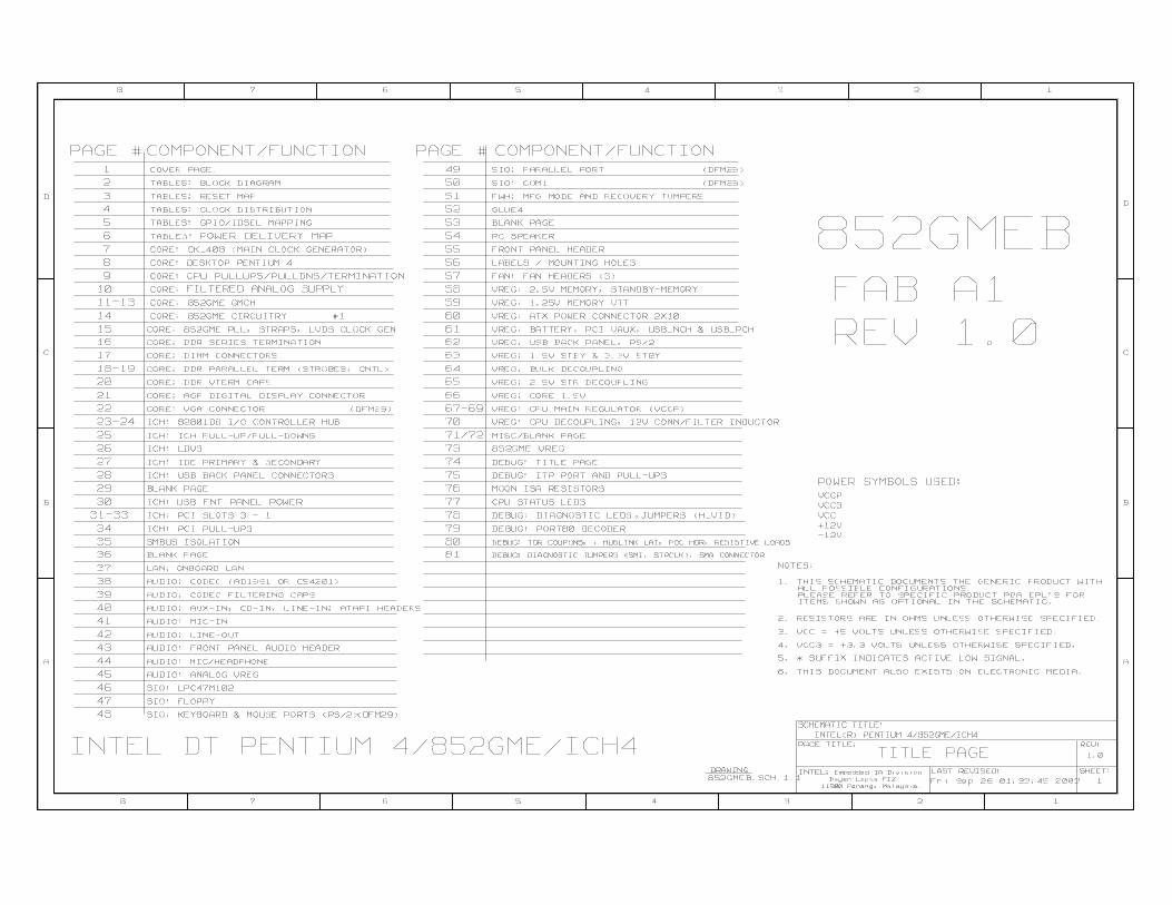


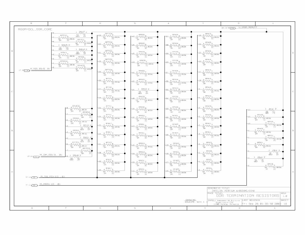


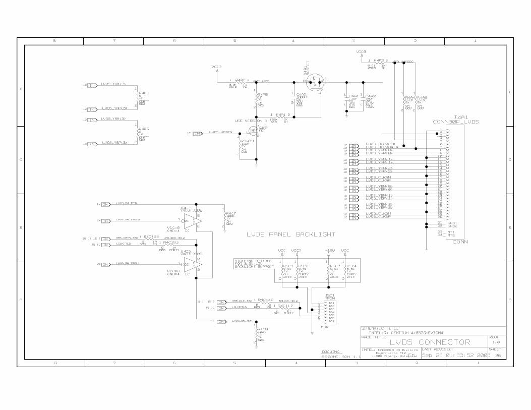


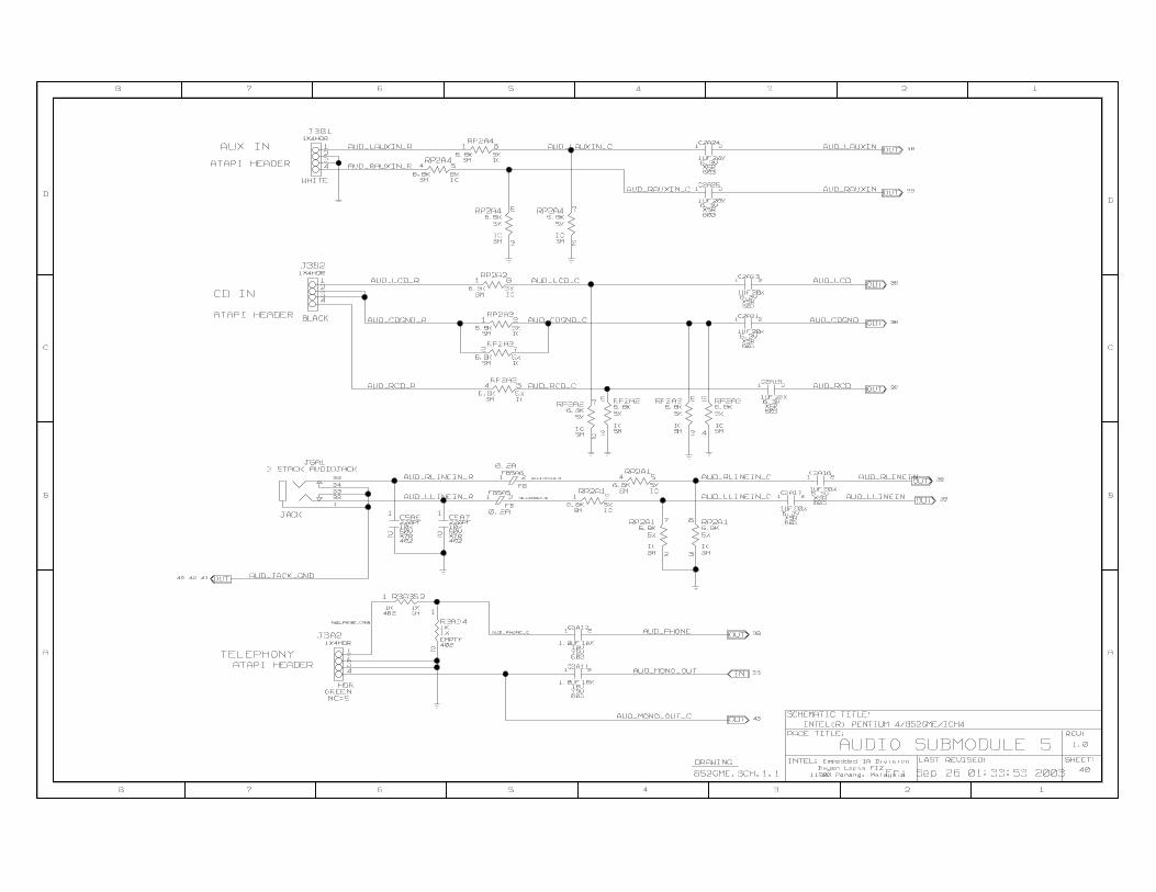


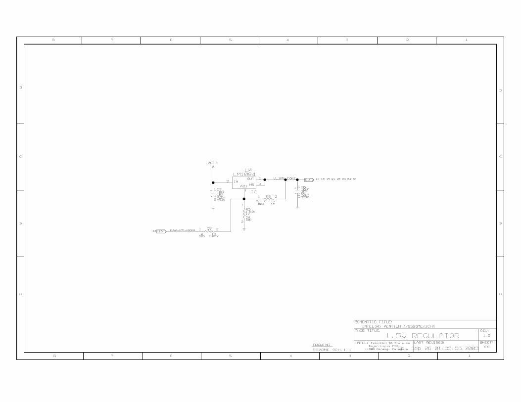


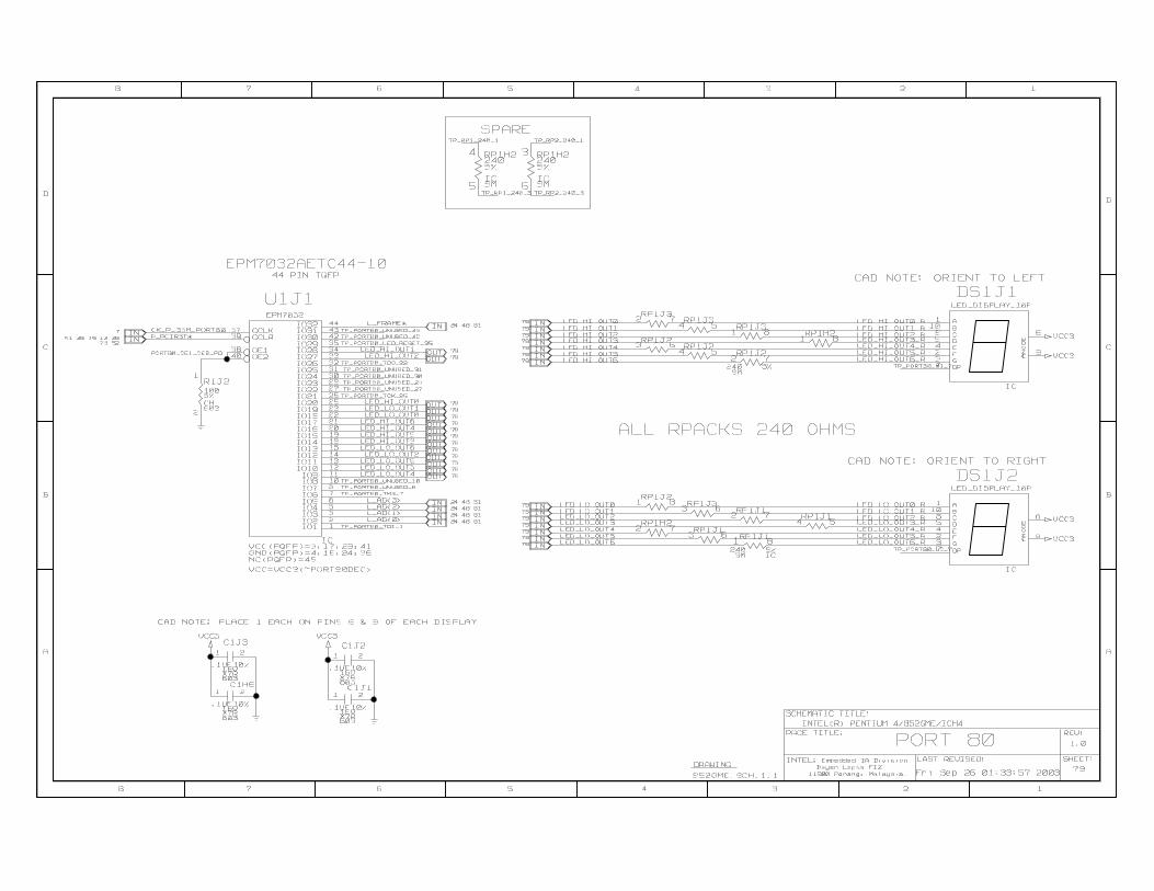

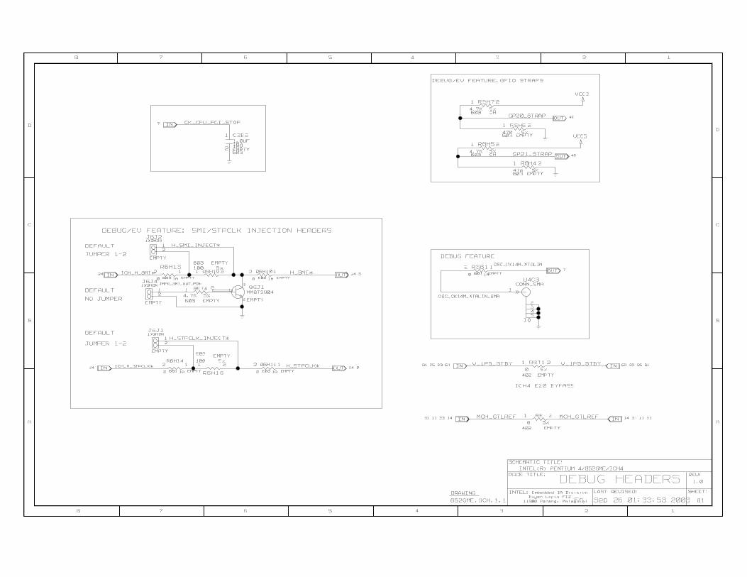

This page intentionally left blank

This page intentionally left blank.
298 Design Guide
Pentium® 4 Processor and Intel® 852GME Chipset PlatformSchematics