CBM2080/CBM1180/CBM1183/CBM2075 - Digchip
17
CBM2080/CBM1180/CBM1183/CBM2075 Datasheet Chipsbank Microelectronics Co., Ltd. West 8 Floor, IER Building, South Area, High-tech Industrial Park, Shenzhen, P.R. China, 518057 Tel: 086-0755-86110580 Fax: 086-0755-86110570 Email: [email protected] URL: http://www.chipsbank.com contained herein. Copyright by Chipsbank Microelectronics Co., Ltd all rights reserved.
-
Upload
khangminh22 -
Category
Documents
-
view
0 -
download
0
Transcript of CBM2080/CBM1180/CBM1183/CBM2075 - Digchip

CBM2080/CBM1180/CBM1183/CBM2075Datasheet
Chipsbank Microelectronics Co., Ltd. West 8 Floor, IER Building, South Area, High-tech Industrial Park, Shenzhen, P.R. China, 518057 Tel: 086-0755-86110580 Fax: 086-0755-86110570 Email: [email protected] URL: http://www.chipsbank.com contained herein. Copyright by Chipsbank Microelectronics Co., Ltd all rights reserved.

iCBM2080/CBM1180 Datasheet -i - March 22, 2005
Contents
1 DESCRIPTION ........................................................................................................................................ 1 2 FEATURES .............................................................................................................................................. 1 3 BLOCK DIAGRAM ................................................................................................................................. 3 4 PIN ASSIGNMENT ................................................................................................................................. 4 4.1 TQFP48 (TOP SIDE) .............................................................................................................................. 4
4.2 CBM2080L/CBM1180L LQFP64 (TOP SIDE) .................................................................................... 5
5 PIN DESCRIPTION................................................................................................................................. 6 6 ELECTRICAL CHARACTERISTICS ................................................................................................... 9 6.1 ABSOLUTE MAXIMUM RATINGS ...................................................................................................... 9
6.2 RECOMMENDED OPERATING CONDITIONS ................................................................................. 9
6.3 STATIC CHARACTERISTICS............................................................................................................... 9
6.4 DYNAMIC CHARACTERISTICS ........................................................................................................ 10
7 TYPICAL APPLICATION ..................................................................................................................... 12 8 MECHANICAL DIMENSIONS............................................................................................................. 13 8.1 48-PIN CBM2080/CBM1180 PACKAGE OUTLINE DIMENSION................................................. 13
8.2 64-PIN CBM2080L/CBM1180L MODE PACKAGE OUTLINE DIMENSION ............................... 14
9 COPYRIGHT NOTICE.......................................................................................................................... 15
1CBM2080/CBM1180 Datasheet -1 - March 22, 2005
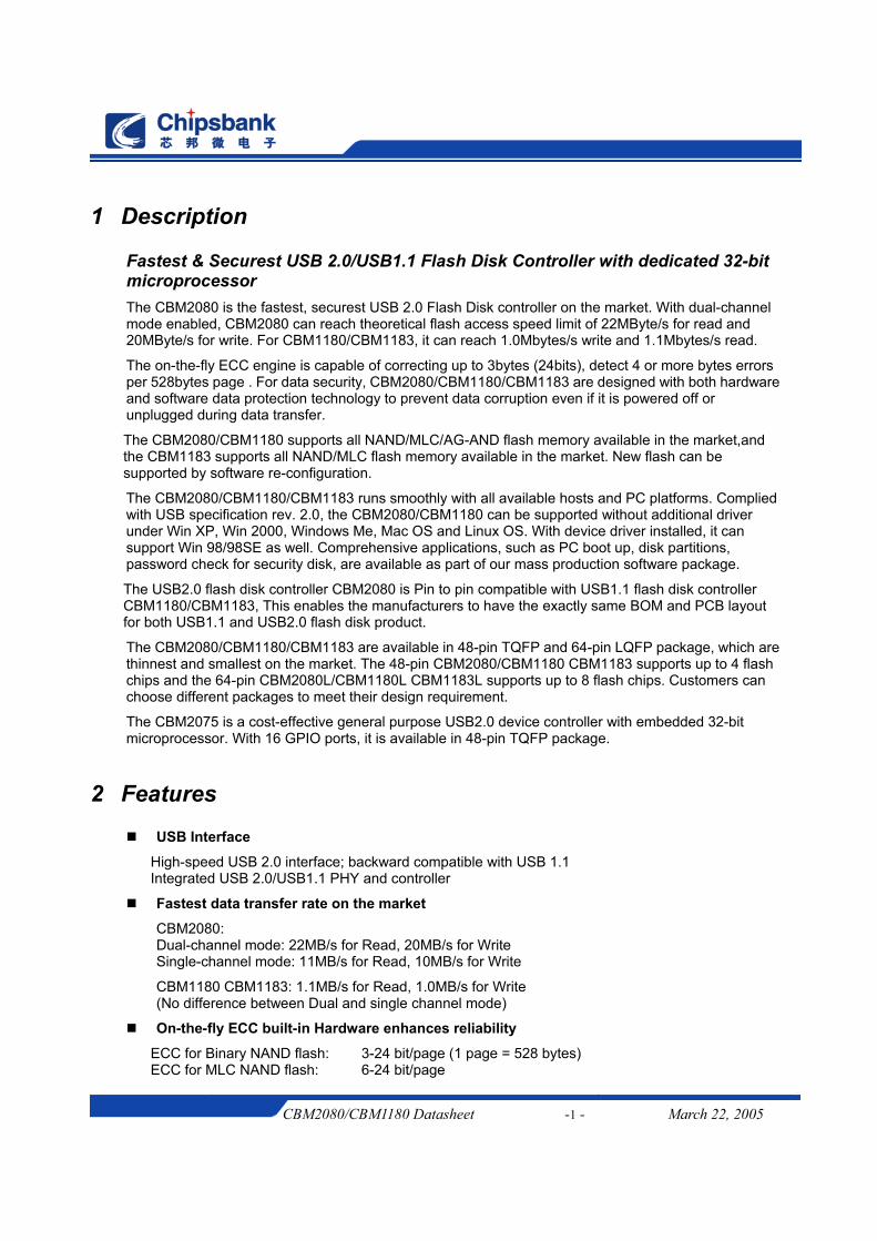
1 Description
Fastest & Securest USB 2.0/USB1.1 Flash Disk Controller with dedicated 32-bit microprocessor
The CBM2080 is the fastest, securest USB 2.0 Flash Disk controller on the market. With dual-channel mode enabled, CBM2080 can reach theoretical flash access speed limit of 22MByte/s for read and 20MByte/s for write. For CBM1180/CBM1183, it can reach 1.0Mbytes/s write and 1.1Mbytes/s read.
The on-the-fly ECC engine is capable of correcting up to 3bytes (24bits), detect 4 or more bytes errors per 528bytes page . For data security, CBM2080/CBM1180/CBM1183 are designed with both hardware and software data protection technology to prevent data corruption even if it is powered off or unplugged during data transfer.
The CBM2080/CBM1180 supports all NAND/MLC/AG-AND flash memory available in the market,and the CBM1183 supports all NAND/MLC flash memory available in the market. New flash can be supported by software re-configuration.
The CBM2080/CBM1180/CBM1183 runs smoothly with all available hosts and PC platforms. Complied with USB specification rev. 2.0, the CBM2080/CBM1180 can be supported without additional driver under Win XP, Win 2000, Windows Me, Mac OS and Linux OS. With device driver installed, it can support Win 98/98SE as well. Comprehensive applications, such as PC boot up, disk partitions, password check for security disk, are available as part of our mass production software package.
The USB2.0 flash disk controller CBM2080 is Pin to pin compatible with USB1.1 flash disk controller CBM1180/CBM1183, This enables the manufacturers to have the exactly same BOM and PCB layout for both USB1.1 and USB2.0 flash disk product.
The CBM2080/CBM1180/CBM1183 are available in 48-pin TQFP and 64-pin LQFP package, which are thinnest and smallest on the market. The 48-pin CBM2080/CBM1180 CBM1183 supports up to 4 flash chips and the 64-pin CBM2080L/CBM1180L CBM1183L supports up to 8 flash chips. Customers can choose different packages to meet their design requirement.
The CBM2075 is a cost-effective general purpose USB2.0 device controller with embedded 32-bit microprocessor. With 16 GPIO ports, it is available in 48-pin TQFP package.
2 Features USB Interface
High-speed USB 2.0 interface; backward compatible with USB 1.1 Integrated USB 2.0/USB1.1 PHY and controller
Fastest data transfer rate on the market
CBM2080: Dual-channel mode: 22MB/s for Read, 20MB/s for Write Single-channel mode: 11MB/s for Read, 10MB/s for Write
CBM1180 CBM1183: 1.1MB/s for Read, 1.0MB/s for Write (No difference between Dual and single channel mode)
On-the-fly ECC built-in Hardware enhances reliability
ECC for Binary NAND flash: 3-24 bit/page (1 page = 528 bytes) ECC for MLC NAND flash: 6-24 bit/page

2CBM2080/CBM1180 Datasheet -2 - March 22, 2005
ECC for AG-AND flash: 6-24 bit/page
Hardware & Software Data Protection Technology
Prevent data corruption even if it is powered off or unplugged during data transfer.
NAND, AG-AND & MLC Flash Interface
Supports Samsung & Toshiba NAND flash memories Supports Toshiba & Sandisk MLC flash memories Supports Renesas AG-AND flash memories Supports Infenion / Hynix flash memories Supports ST Microelectronics flash memories Supports Micron / Actrans flash memories Software configuration to support various new flash memories Supports up to 8 flash chips.
Proprietary 32-bit CISC microprocessor feature
Proprietary 32-bit CISC processor for USB protocol processing and flash access.
Single cycle instruction period
Write-protect switch for security
Integrated 3.3v to 1.8v voltage regulator
LED indicator to show access status
Three modes: Busy, waiting, and off
Disk partitions and password check for security disk available
PC boot up as USB Zip Disk and USB Hard Disk
Auto run function
USB suspend and resume
Low power dissipation
Operating current 50mA (Bus power compatible)
Leading 0.18um CMOS technology
48-pin TQFP /64-pin LQFP package
48-pin CBM2080/CBM1180/CBM1183 supports up to 4 Flash Chips 64-pin CBM2080L/CBM1180L/CBM1183L supports up to 8 Flash Chips
Windows, Mac and Linux compatible

3CBM2080/CBM1180 Datasheet -3 - March 22, 2005
3 Block Diagram

4CBM2080/CBM1180 Datasheet -4 - March 22, 2005
4 Pin Assignment
4.1 TQFP48 (Top Side)

5CBM2080/CBM1180 Datasheet -5 - March 22, 2005
4.2 LQFP64 (Top Side)
6CBM2080/CBM1180 Datasheet -6 - March 22, 2005
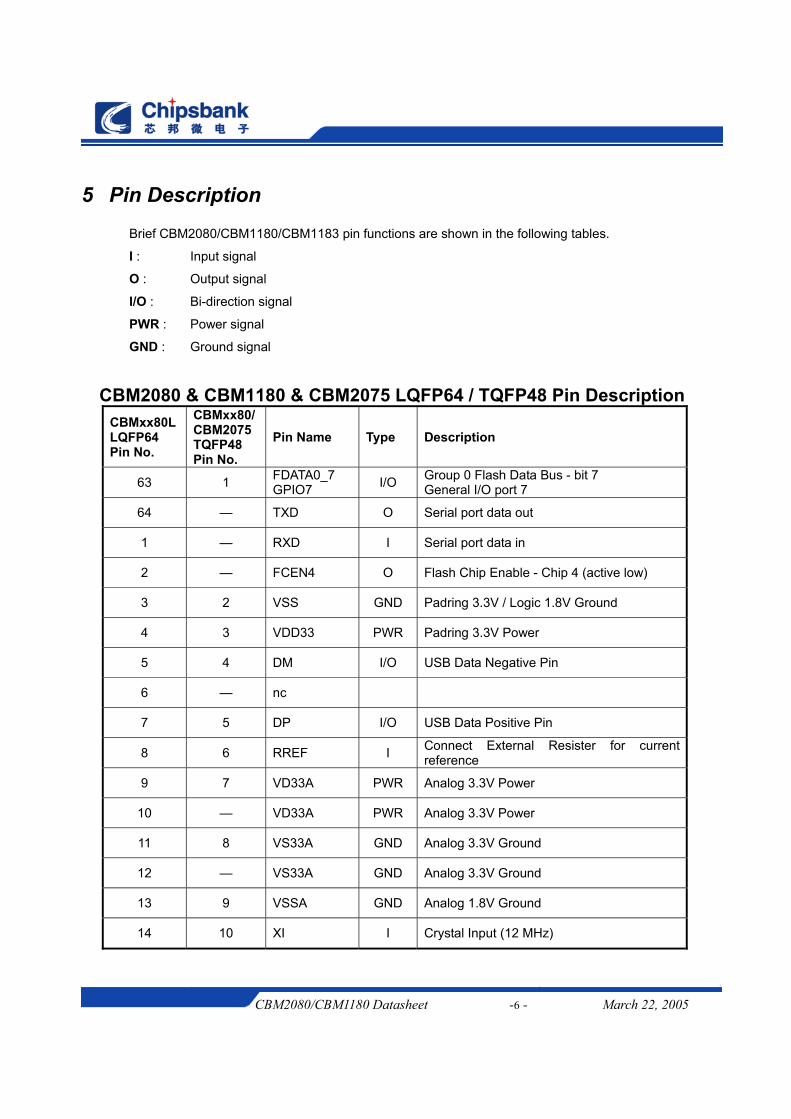
5 Pin Description Brief CBM2080/CBM1180/CBM1183 pin functions are shown in the following tables.
I : Input signal
O : Output signal
I/O : Bi-direction signal
PWR : Power signal
GND : Ground signal
CBM2080 & CBM1180 & CBM2075 LQFP64 / TQFP48 Pin Description CBMxx80L LQFP64 Pin No.
CBMxx80/CBM2075 TQFP48 Pin No.
Pin Name Type Description
63 1 FDATA0_7 GPIO7 I/O Group 0 Flash Data Bus - bit 7
General I/O port 7
64 — TXD O Serial port data out
1 — RXD I Serial port data in
2 — FCEN4 O Flash Chip Enable - Chip 4 (active low)
3 2 VSS GND Padring 3.3V / Logic 1.8V Ground
4 3 VDD33 PWR Padring 3.3V Power
5 4 DM I/O USB Data Negative Pin
6 — nc
7 5 DP I/O USB Data Positive Pin
8 6 RREF I Connect External Resister for current reference
9 7 VD33A PWR Analog 3.3V Power
10 — VD33A PWR Analog 3.3V Power
11 8 VS33A GND Analog 3.3V Ground
12 — VS33A GND Analog 3.3V Ground
13 9 VSSA GND Analog 1.8V Ground
14 10 XI I Crystal Input (12 MHz)

7CBM2080/CBM1180 Datasheet -7 - March 22, 2005
15 11 XO O Crystal Output
16 12 VDDA PWR Analog 1.8V Power
17 — GPI0 I/O General Input port 0
18 — GPI1 I/O General Input port 1
19 13 WP I Write Protect Switch Input
20 14 RESET_ I Reset Sign (active low)
21 15 FWRN1 O Group 1 Flash Write Enable (active low)
22 16 FRDN1 O Group 1 Flash Read Enable (active low)
23 17 LED O LED Indication
24 18 FRB1 GPI5 I Group 1 Flash Ready_Busy
General Input port 5
25 19 TEST_MODE I Test Mode Enable Pin
26 20 BT_SEL I Boot up selection
27 21 FDATA1_0 GPIO8 I/O Group 1 Flash Data Bus - bit 0
General I/O port 8
28 22 FDATA1_1 GPIO9 I/O Group 1 Flash Data Bus - bit 1
General I/O port 9
29 23 FDATA1_2 GPIO10 I/O Group 1 Flash Data Bus - bit 2
General I/O port 10
30 24 FDATA1_3 GPIO11 I/O Group 1 Flash Data Bus - bit 3
General I/O port 11
31 — GPI2 I/O General Input port 2
32 — GPI3 I/O General Input port 3
33 — FCEN5 O Flash Chip Enable - Chip 5(active low)
34 25 FDATA1_4 GPIO12 I/O Group 1 Flash Data Bus - bit 4
General I/O port 12
35 26 FDATA1_5 GPIO13 I/O Group 1 Flash Data Bus - bit 5
General I/O port 13
36 — FCEN3 O Flash Chip Enable - Chip 3 (active low)
37 27 VDD33 PWR Padring 3.3V Power
38 28 FDATA1_6 GPIO14 I/O Group 1 Flash Data Bus - bit 6
General I/O port 14
39 29 FDATA1_7 GPIO15 I/O Group 1 Flash Data Bus - bit 7
General I/O port 15
40 30 FALE1 GPO3 O Group 1 Flash Address Latch Enable
General Output port 3
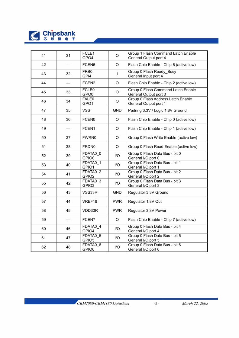
8CBM2080/CBM1180 Datasheet -8 - March 22, 2005
41 31 FCLE1 GPO4 O Group 1 Flash Command Latch Enable
General Output port 4
42 — FCEN6 O Flash Chip Enable - Chip 6 (active low)
43 32 FRB0 GPI4 I Group 0 Flash Ready_Busy
General Input port 4
44 — FCEN2 O Flash Chip Enable - Chip 2 (active low)
45 33 FCLE0 GPO0 O Group 0 Flash Command Latch Enable
General Output port 0
46 34 FALE0 GPO1 O Group 0 Flash Address Latch Enable
General Output port 1
47 35 VSS GND Padring 3.3V / Logic 1.8V Ground
48 36 FCEN0 O Flash Chip Enable - Chip 0 (active low)
49 — FCEN1 O Flash Chip Enable - Chip 1 (active low)
50 37 FWRN0 O Group 0 Flash Write Enable (active low)
51 38 FRDN0 O Group 0 Flash Read Enable (active low)
52 39 FDATA0_0 GPIO0 I/O Group 0 Flash Data Bus - bit 0
General I/O port 0
53 40 FDATA0_1 GPIO1 I/O Group 0 Flash Data Bus - bit 1
General I/O port 1
54 41 FDATA0_2 GPIO2 I/O Group 0 Flash Data Bus - bit 2
General I/O port 2
55 42 FDATA0_3 GPIO3 I/O Group 0 Flash Data Bus - bit 3
General I/O port 3
56 43 VSS33R GND Regulator 3.3V Ground
57 44 VREF18 PWR Regulator 1.8V Out
58 45 VDD33R PWR Regulator 3.3V Power
59 — FCEN7 O Flash Chip Enable - Chip 7 (active low)
60 46 FDATA0_4 GPIO4 I/O Group 0 Flash Data Bus - bit 4
General I/O port 4
61 47 FDATA0_5 GPIO5 I/O Group 0 Flash Data Bus - bit 5
General I/O port 5
62 48 FDATA0_6 GPIO6 I/O Group 0 Flash Data Bus - bit 6
General I/O port 6

9CBM2080/CBM1180 Datasheet -9 - March 22, 2005
6 Electrical Characteristics
6.1 Absolute maximum ratings In accordance with the Absolute Maximum Rating System (IEC 60134).
symbol parameter conditions min max unit
VCCA analog supply voltage -0.5 5.5 v
VCCD digital supply voltage -0.5 4.5 v
VI input voltage -0.5 5.5 v
DP, DM and GND pins -4000 +4000
Vesd electrostatic discharge voltage[1]
ILI < 1 A other pins -2000 +2000
v
Tstg storage temperature -40 +125 ℃
[1] Equivalent to discharging a 100 pF capacitor via a 1.5 k resistor (Human Body Model).
6.2 Recommended operating conditions
symbol Parameter conditions min Typ max Unit
VCCA analog supply voltage 3.0 3.3 3.6 V
VCCD digital supply voltage 3.0 3.3 3.6 V
VI input voltage 0 - VCCD V
Low/Full speed 0 3.3 3.6 V VI(AI/O) input voltage on analog
I/O pins DP DM High speed 0 400 - mV
Tamb ambient temperature 0 - +70 ℃
6.3 Static characteristics All parameters are measured at VCCA = VCCD = 3.0 to 3.6 V; VAGND = VDGND = 0 V; Tamb = 40 to 85 ℃;
symbol Parameter Conditions min Typ max Unit
Full-speed transmitting and receiving; - 29.5 -
ICC operating supply current high-speed transmitting and
receiving - 50 mA
ICC(susp) suspend supply current in suspend mode - 500 uA

10CBM2080/CBM1180 Datasheet -10 - March 22, 2005
6.4 Dynamic characteristics All parameters are measured at VCCA = VCCD = 3.0 to 3.6 V; VAGND = VDGND = 0 V; Tamb = 40 to 85 ℃ ;
symbol Parameter conditions min Typ max Unit
Ts(FDATA*) FDATA* setup time relative to rising FWRN* edge - 33 - ns
Th(FDATA*) FDATA* hold time relative to falling FWRN* edge - 33 - ns
Ts (FCLE*) FCLE* setup time relative to falling FWRN* edge - 33 - ns
Th (FCLE*) FCLE* hold time relative to rising FWRN* edge - 33 - ns
Ts (FALE*) FALE* setup time relative to falling FWRN* edge - 33 - ns
Th (FALE*) FALE* hold time relative to rising FWRN* edge - 33 - ns
Ts (FCEN*) FCEN* setup time relative to falling FWRN* edge - 99 - ns
Tpw (FWRN*) FWRN* Pulse Width - 33 - ns
Thh (FWRN*) FWRN* high hold time - 33 - ns
Ta(FDATA*) FDATA* access time relative to falling FRDN* edge - - 40 ns
Tpw (FRDN*) FWRN* Pulse Width - 33 - ns
Thh (FRDN*) FWRN* high hold time - 33 - ns
Timing diagram for Writing of Data
Timing diagram for Reading of Data

11CBM2080/CBM1180 Datasheet -11 - March 22, 2005

CBM2080/CBM1180 Datasheet --12 -- March 22, 2005
7 Typical Application

13CBM2080/1180 Datasheet - 13 - March 22, 2005
8 Mechanical Dimensions
8.1 48-Pin CBM2080/CBM1180/CBM1183 Package Outline Dimension
14CBM2080/1180 Datasheet - 14 - March 22, 2005
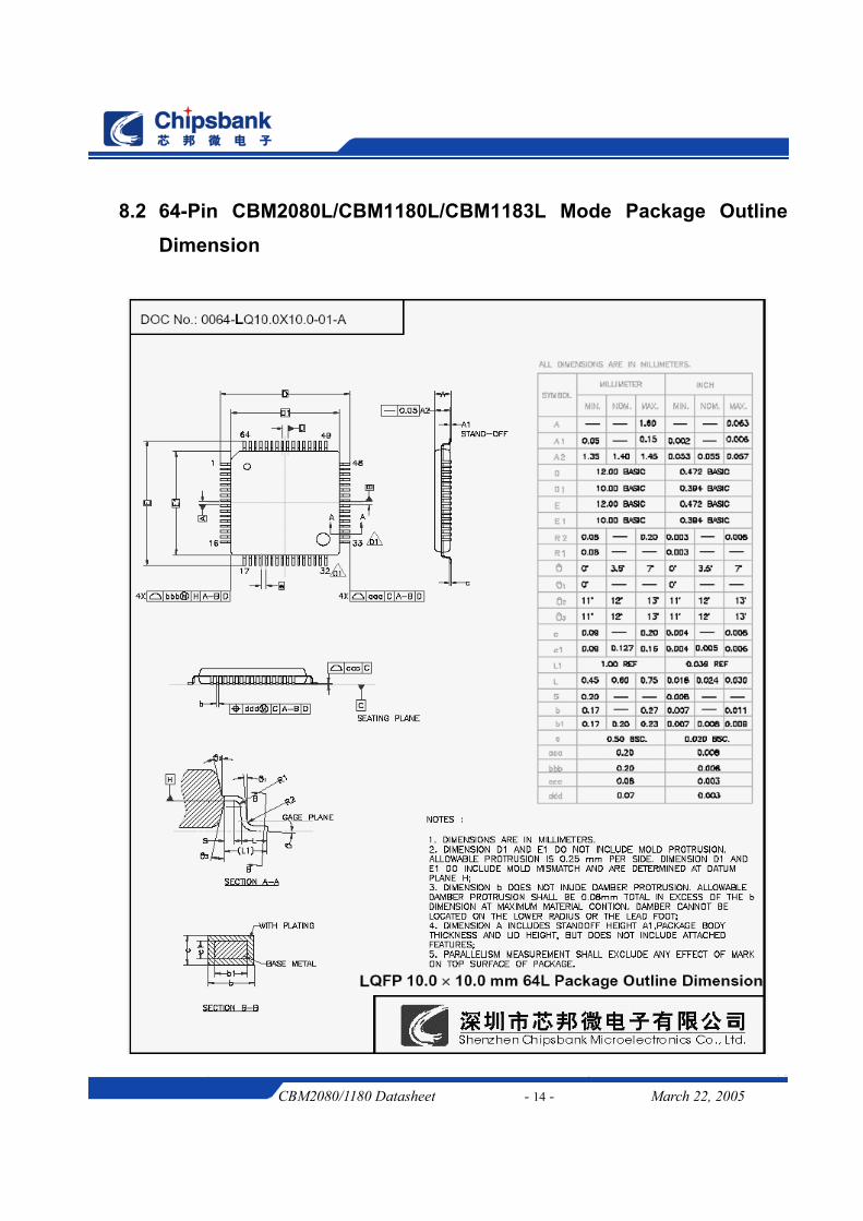
8.2 64-Pin CBM2080L/CBM1180L/CBM1183L Mode Package Outline Dimension

CBM2080/CBM1180 Datasheet - 15 - March 22, 2005
9 Copyright Notice Copyright 2004 by Chipsbank Microelectronics Co. Ltd. All Rights Reserved.
Right to make changes —Chipsbank Microelectronics Co., Ltd reserves the right to make changes in the products - including circuits, standard cells, and/or software - described or contained herein in order to improve design and/or performance. The information contained in this manual is provided for the general use by our customers. Our customers should be aware that the personal computer field is the subject of many patents. Our customers should ensure that they take appropriate action so that their use of our products does not infringe upon any patents. It is the policy of Chipsbank Microelectronics Co., Ltd. to respect the valid patent rights of third parties and not to infringe upon or assist others to infringe upon such rights.
This manual is copyrighted by Chipsbank Microelectronics Co., Ltd. You may not reproduce, transmit, transcribe, store in a retrieval system, or translate into any language, in any form or by any means, electronic, mechanical, magnetic, optical, chemical, manual, or otherwise, any part of this publication without the expressly written permission from Chipsbank Microelectronics Co., Ltd.