INTEL Ex.1035.001 - NET
350
INTEL Ex.1035.001
-
Upload
khangminh22 -
Category
Documents
-
view
2 -
download
0
Transcript of INTEL Ex.1035.001 - NET

INTEL Ex.1035.001

INTEL Ex.1035.002

INTEL Ex.1035.003
····rm11r11HHr-· 1 aoooo6534 t D f" •1. T . . F I _._. ... ..., ... ..:;:" Mr .. nnec ure e 1n1 ions, r1v1a, ormu as,
and Rules of Thumb
Definitions
Big Endian: the byte with the binary address "x ... xOO" is in the most significant position ("big end") of a 32-bit word (page 95).
Clock rate: inverse of clock cycle time, usually measured in MHz (page 36). CPI: clock cycles per instruction (page 36). Hit rate: fraction of memory references found in the cache, equal to 1-Miss rate (page 404). Hit time: memory-access time for a cache hit, including time to determine if hit or miss (page 405). Instruction count: number of instructions executed while running a program (page 36). Little Endian: the byte with the binary address "x ... xOO" is in the least significant position
("little end") of a 32-bit word (page 95). MIMD: (multiple instruction stream, multiple data stream) a multiprocessor or multicomputer
(page 572). Miss penalty: time to replace a block in the top level of a cache system with the corresponding block
from the lower level (page 405). Miss rate: fraction of memory references not found in the cache, equal to 1 - Hit rate (page 404 ). N112: the vector length needed to reach one-half of R00 (page 384). Nv: the vector length needed so that vector mode is faster than scalar mode (page 384). R
00: the megaflop rate of an infinite-length vector (page 384).
RAW data hazard: (read after write) instruction tries to read a ~ource before a prior instruction writes it; so it incorrectly gets the old value (page 264).
SIMD: (single instruction stream, multiple data stream) an array processor (page 572). SISD: (single instruction stream, single data stream) a uniprocessor (page 572). Spatial locality: (locality in space) if an item is referenced, nearby items will tend to be referenced
soon (page 403). Temporal locality: (locality in time) if an item is referenced, it will tend to be referenced again soon
(page 403). WAR data hazard: (write after read) instruction tries to write a destination before it is read by a prior
instruction, so prior instruction incorrectly gets the new value (page 264). WAW data hazard: (write after write) instruction tries to write an operand before it is written by a
prior instruction. The writes are performed in the wrong order, incorrectly leaving the value of the prior instruction in the destination (page 264).
Trivia
Byte order of machines (page 95)
Big Endian: IBM 360, MIPS, Motorola, SPARC, DLX Little Endian: DEC VAX, DEC RISC, Intel 80x86
Year and User Address Size of Generations of IBM and Intel Computer Families
Year Model User address size Year Model User address size ~
1964 IBM360 24 1978 Intel 8086 4+16
1971 IBM370 24 1981 Intel 80186 4+16
1983 IBM370-XA 31 1982 Intel 80286 16+16
1986 IBMESA/370 16+31 1985 Intel 80386 16+32 or 32
1989 Intel 80486 16+32 or 32
INTEL Ex.1035.004

Formulas
1 1. Amdahl's Law: Speedup=---------------
. Fractionenhanced (page 8)
( l-Fract10nenhanced) + S d pee UPenhanced
2. CPU time= Instruction count* Clock cycles per instruction* Clock cycle time (page 36)
3 Average memory-access time = Hit time + Miss rate * Miss penalty (page 405)
4. Means-arithmetic(AM), weighted arithmetic(W AM), harmonic(HM) and weighted harmonic(WHM): n n
AM= l L,Timei, WAM = L,Weighti * Timei, HM= n , WHM = l n. 1 . 1 n n
l= l= ~ 1 ~Weighti ~Ratei ..£...J Ratei i=l i=l
where Timei is the execution time for the ith program of a total of n in the workload, W eighti is the weighting of the ith program in the workload, and Ratei is a function of l!fimei (page 51).
C .-r . d . . _ Cost of die + Cost of testing die + Cost of packaging (page 55
) 5. ost o1 integrate circuit - p· 1 t t · ld ma es y1e
6 D . . Id W .c • ld { 1 Defects per unit area * Die area }--ex . ie yie = aier y1e * + a
where Wafer yield accounts for wafers that are so bad they need not be tested and a corresponds to the number of masking levels critical to die yield (usually a 2:: 2.0, page 59).
p . 1. d _ Clock cycle timen0 pipelining * Ideal CPI * Pipeline depth
7 · ipe me spee up - Clock cycle timepipelined Ideal CPI + Pipeline stall cycles per instruction
where Pipeline stall cycles accounts for clock cycles lost due to pipeline hazards (page 258).
8. System performance: . Timecpu Timeuo Time0 verlap
T1meworkload = S d + S d M · (S d S d pee upcpu pee up1;0 ax1mum pee upcpu, pee up11o)
where Timecpu means the time the CPU is busy, Time1;0 means the time the I/0 system is busy, and Timeoverlap means the time both are busy. This formula assumes the overlap scales linearly with speedup (page 506).
Rules of Thumb
1. Amdahl/Case Rule: A balanced compu,ter system need~ about 1 megabyte of main memory capacity and 1 megabit per second of I/0 bandwidth per MIPS of CPU performance (page 17).
2. 90110 Locality Rule: A program executes about 90% of its instructions in 10% of its code (pages 11-12).
3. DRAM-Growth Rule: Density increases by about 60% per year, quadrupling in 3 years (page 17). 4. Disk-Growth Rule: Den~ity increases by about 25% per year, doubling in 3 years (page 17). 5. Address-Consumption Rule: The memory needed by the average program grows by about a factor
of 1.5 to 2 per year; thus, it consumes between 1/2 and 1 address bit per year (page 16). 6. 90150 Branch-Taken Rule: About 90% of backward-going branches are taken while about 50% of
forward-going branches are taken (page 108). 7. 2:1 Cache Rule: The miss rate of a direct-mapped cache of size Xis about the same as a 2-way
set-associative cache of size X/2 (page 421).
INTEL Ex.1035.005

INTEL Ex.1035.006

Computer Architecture
A Quantitative
Approach
INTEL Ex.1035.007

INTEL Ex.1035.008

Computer Architecture
A Quantitative Approach
David A. Patterson UNIVERSITY OF CALIFORNIA AT BERKELEY
John L. Hennessy STANFORD UNIVERSITY
With a Contribution by David Goldberg
Xerox Palo Alto Research Center
MORGAN KAUFMANN PUBLISHERS, INC. SAN MATEO, CALIFORNIA
INTEL Ex.1035.009

Sponsoring Editor Bruce Spatz Production Manager Shirley Jowell Technical Writer Walker Cunningham Text Design Gary Head Cover Design David Lance Goines Copy Editor Linda Medoff Proofreader Paul Medoff Computer Typesetting and Graphics Fifth Street Computer Services
Library of Congress Cataloging-in-Publication Data Patterson, David A.
Computer architecture : a quantitative approach I David A. Patterson, John L. Hennessy
p. cm. Includes bibliographical references ISBN 1-55860- 069-8 1. Computer architecture. I. Hennessy, John L. II. Title.
QA76.9.A73P377 1990 004.2'2--dc20
Morgan Kaufmann Publishers, Inc.
Editorial Office: 2929 Campus Drive. San Mateo, CA 94403
Order from: P.O. Box 50490, Palo Alto, CA 94303-9953
© 1990 by Morgan Kaufmann Publishers, Inc. All rights reserved.
89-85227 CIP
No part of this publication may be reproduced, stored in a retrieval system, or transmitted in any form or by any means-electronic, mechanical, recording, or otherwise-without the prior permission of the publisher.
All instruction sets and other design information of the DLX computer system contained herein is copyrighted by the publisher and may not be incorporated in other publications or distributed by media without formal acknowledgement and written consent from the publisher. Use of the DLX in other publications for educational purposes is encouraged and application for permission is welcomed.
ADVICE, PRAISE, & ERRORS: Any correspondence related to this publication or intended for the authors should be addressed to the editorial offices of Morgan Kaufmann Publishers, Inc., Dept. P&H APE. Information regarding error sightings is encouraged. Any error sightings that are accepted for correction in subsequent printings will be rewarded by the authors with a payment of $1.00 (U.S.) per correction upon availability of the new printing. Electronic mail can be sent to [email protected]. (Please include your full name and permanent mailing address.)
INSTRUCTOR SUPPORT: For information on classroom software and other instructor materials available to adopters, please contact the editorial offices of Morgan Kaufmann Publishers, Inc. (415) 578-9911.
Third printing, i993
INTEL Ex.1035.010

To Andrea, Linda, and our four sons
INTEL Ex.1035.011

Trademarks The following trademarks are the property of the following organizations:
Alliant is a trademark of Alliant Computers. 3090/600, 3090/600S, 3090 VF, 3330, 3380, 3380D, 3380 Disk Model AMD 29000 is a trademark of AMD. AK4, 3380J, 3390, 3880-23, 3990, 7030, 7090, 7094, IBM FORTRAN,
TeX is a trademark of American Mathematical Society.
AMI 6502 is a trademark of AMI.
Apple I, Apple II, and Macintosh are trademarks of Apple Computer, Inc.
ZS- I is a trademark of Astronautics.
UNIX and UNIX F77 are trademarks of AT&T Bell Laboratories.
Turbo C is a trademark of Borland International.
The Cosmic Cube is a trademark of California Institute of Technology.
Warp, C.mmp, and Cm* are trademarks of Carnegie-Mellon University.
CP3 IOO is a trademark of Conner Peripherals.
CDC 6600, CDC 7600, CDC STAR-100, CYBER-180, CYBER 180/990, and CYBER-205 are trademarks of Control Data Corporation.
Conve~, C-1, C-2, and C series are trademarks of Convex.
CRA Y-3 is a trademark of Cray Computer Corporation.
CRAY-I, CRAY-IS, CRAY-2, CRAY X-MP, CRAY X-MP/416, CRAY Y-MP, CFT77 V3.0, CFT, and CFT2 Vl.3a are trademarks of Cray Research.
Cydra 5 is a trademark of Cydrome.
CY7C601, 7C601, 7C604, and 7C157 are trademarks of Cypress Semiconductor.
Nova is a trademark of Data General Corporation.
HEP is a trademark of Denelcor.
CV AX, DEC, DECsystem, DECstation, DECstation 3100, DECsystem 10/20, fort, LPl I, Massbus, MicroVAX-I, MicroVAX-II, PDP-8, PDP-10, PDP-I I, RS-1 !M/IAS, Unibus, Ultrix, Ultrix 3.0, VAX, V AXstation, V AXstation 2000, V AXstation 3100, VAX-I I, VAX-11/780, V AX-11/785, VAX Model 730, Model 750, Model 780, VAX 8600, VAX 8700, VAX 8800, VS FORTRAN V2.4, and VMS are trademarks of Digital Equipment Corporation.
BINAC is a trademark of Eckert-Mauchly Computer Corporation.
Multimax is a trademark of Encore Computers.
ET A 10 is a trademark of the ET A Corporation.
SYMBOL is a trademark of Fairchild Corporation.
Pegasus is a trademark of Ferranti, Ltd.
Ferrari and Testarossa are trademarks of Ferrari Motors.
AP-120B is a trademark of Floating Point Systems.
Ford and Escort are trademarks Ford Motor Co.
Gnu C Compiler is a trademark of Free Software Foundation.
M2361A, Super Eagle, VPlOO, and VP200 are trademarks of Fujitsu Corporation.
Chevrolet and Corvette are trademarks of General Motors Corporation.
HP Precision Architecture, HP 850, HP 3000, HP 3000/70, Apollo DN 300, Apollo DN 10000, and Precision are trademarks of Hewlett-Packard Company.
S810, S810/200, and S820 are trademarks of Hitachi Corporation.
Hyundai and Excel are trademarks of the Hyundai Corporation.
432, 960 CA, 4004, 8008, 8080, 8086, 8087, 8088, 80186, 80286, 80386, 80486, iAPX 432, i860, Intel, Multibus, Multibus II, and Intel Hypercube are trademarks of Intel Corporation.
Inmos and Transputer are trademarks of Inmos.
Clipper ClOO is a trademark of Intergraph.
IBM, 360, 360/30, 360/40, 360/50, 360/65, 360/85, 360/91, 370, 370/135, 370/138, 370/145, 370/155, 370/158, 370/165, 370/168, 370-XA, ESA/370, System/360, System/370, 701, 704, 709, 801, 3033, 3080, 3080 series, 3080 VF, 3081, 3090, 3090/100, 3090/200, 3090/400,
ISAM, MYS, IBM PC, IBM PC-AT, PL.8, RT-PC, SAGE Stretch IBM SYS, Vector Facility, and VM are trademarks of Inte~ationai Business Machines Corporation.
FutureBus is a trademark of the Institute of Electrical and Electronic Engineers.
Lamborghini and Countach are trademarks of Nuova Automobili Ferrucio Lamborghini, SP A.
Lotus 1-2-3 is a trademark of Lotus Development Corporation.
MB8909 is a trademark of LSI Logic.
NuBus is a trademark of Massachusetts Institute of Technology.
Miata and Mazda are trademarks of Mazda.
MASM, Microsoft Macro Assembler, MS DOS, MS DOS 3.1, and OS/2 are trademarks of Microsoft Corporation.
MIPS, MIPS 120, MIPS/120A, M/500, M/1000, RC6230, RC6280, R2000, R2000A, R2010, R3000, and R3010 are trademarks of MIPS Computer Systems.
Delta Series 8608, System V/88 R32V!, VME bus, 6809, 68000, 68010, 68020, 68030, 68882, 88000, 88000 l.8.4ml4, 88100, and 88200 are trademarks of Motorola Corporation.
Multiflow is a trademark of Multiflow Corporation.
National 32032 and 32x32 are trademarks of National Semiconductor Corporation.
Ncube is a trademark of Ncube Corporation.
SX/2, SX/3, and FORTRAN 77/SX V.040 are trademarks of NEC Information Systems.
NYU Ultracomputer is a trademark of New York University.
VAST-2 v.2.21 is a trademark of Pacific Sierra.
Wren IV, Imprimis, Sabre, Sabre 97209, and IPI-2 are trademarks of Seagate Corporation.
Sequent, Balance 800, Balance 21000, and Symmetry are trademarks of Sequent Computers.
Silicon Graphics 4D/60, 4D/240, and Silicon Graphics 4D Series are trademarks of Silicon Graphics.
Stellar GS 1000, Stardent-1500, and Ardent Titan-I are trademarks of Stardent.
Sun 2, Sun 3, Sun 3/75, Sun 3/260, Sun 3/280, Sun 4, Sun 4/110, Sun 4/260, Sun 4/280, SunOS 4.0.3c, Sun 1.2 FORTRAN compiler, SPARC, and SPARCstation I are trademarks of Sun Microsystems.
Synapse N+ I is a trademark of Synapse.
Tandem and Cyclone are trademarks of Tandem Computers.
TI 8847 and TI ASC are trademarks of Texas Instruments Corporation.
Connection Machine and CM-2 are trademarks of Thinking Machines.
Burroughs 6500, B5000, B5500, D-machine, UNIV AC, UNIV AC I, UNIV AC 1103 are trademarks of UNISYS.
Spice and 4.2 BSD UNIX are trademarks of University of California, Berkeley.
Illiac, Illiac IV, and Cedar are trademarks of University of Illinois.
Ada is a trademark of the U.S. Government (Ada Joint Program Office).
Weitek 3364, Weitek 1167, WTL 3110, and WTL 3170 are trademarks of Weitek Computers.
Alto, Ethernet, PARC, Palo Alto Research Center, Smalltalk, and Xerox are trademarks of Xerox Corporation.
Z-80 is a trademark of Zilog.
INTEL Ex.1035.012

Foreword by C. Gordon Bell
I am delighted and honored to write the foreword for this landmark book. The authors have gone beyond the contributions of Thomas to Calculus and
Samuelson to Economics. They have provided the definitive text and reference for computer architecture and design. To advance computing, I urge publishers to withdraw the scores of books on this topic so a new breed of architect/ engineer can quickly emerge. This book won't eliminate the complex and errorful microprocessors from semicomputer companies, but it will hasten the education of engineers who can design better ones.
The book presents the critical tools to analyze uniprocessor computers. It shows the practicing engineer how technology changes over time and offers the empirical constants one needs for design. It motivates the designer about function, which is a welcome departure from the usual exhaustive shopping list of mechanisms that a naive designer might attempt to include in a single design.
The authors establish a baseline for analysis and comparisons by using the most important machine in each class: mainframe (IBM 360), mini (DEC VAX), and micro/PC (Intel 80x86). With this foundation, they show the coming mainline of simpler pipelined and parallel processors. These new technologies are shown as variants of their pedagogically useful, but highly realizable, processor (DLX). The authors stress technology independence by measuring work done per clock (parallelism), and time to do work (efficiency and latency). These methods should also improve the quality of research on new architectures and parallelism.
Thus, the book is required understanding for anyone working with architecture or hardware, including architects, chip and computer system engineers, and compiler and operating system engineers. It is especially useful for software engineers writing programs for pipelined and vector computers. Managers and marketers will benefit by knowing the Fallacies and Pitfalls sections of the book. One can lay the demise of many a computer-and, occasionally, a company--on engineers who fail to understand the subtleties of computer design.
The first two chapters establish the essence of computer design through measurement and the understanding of price/performance. These concepts are applied to the instruction set architecture and how it is measured. They discuss the implementation of processors and include extensive discussions of techniques for designing pipelined and vector processors. Chapters are also devoted to memory hierarchy and the often-neglected input/output. The final chapter
ix
INTEL Ex.1035.013

x Foreword
presents the opportunities and questions about machines and directions of the future. Now, we need their next book on how to build these machines.
The reason this book sets a standard above all others and is unlikely to be superseded in any foreseeable future is the understanding, experience, taste, and uniqueness of the authors. They have stimulated the major change in architecture by their work on RISC (Patterson coined the word). Their university research leading to product development at MIPS and Sun Microsystems established important architectures for the 1990s. Thus, they have done the analysis, evaluated the trade-offs, worked on the compilers and operating systems, and seen their machines achieve significance in use. Furthermore, as teachers, they have seen that the book is pedagogically sound (and have solicited opinions from others through the unprecedented Beta testing program). I know this will be the book of the decade in computer systems. Perhaps its greatest accomplishment would be to stimulate other great architects and designers of higher-level systems (databases, communications systems, languages and operating systems) to write similar books about their domains.
I've already enjoyed and learned from the book, and surely you will too.
-C. Gordon Bell
INTEL Ex.1035.014
Computer Architecture: A Quantitative Approach xi
Contents
Foreword ix by C. GORDON BELL
Preface xvii
Acknowledgements xx iii
1 Fundamentals of Computer Design 2 1.1 Introduction 3 1.2 Definitions of Performance 5 1.3 Quantitative Principles of Computer Design 8 1.4 The Job of a Computer Designer 13 1.5 Putting It All Together: The Concept of Memory Hierarchy 18 1.6 Fallacies and Pitfalls 21 1.7 Concluding Remarks 22 1.8 Historical Perspective and References 23
Exercises 28
2 Performance and Cost 32 2.1 Introduction 33 2.2 Performance 35 2.3 Cost 53 2.4 Putting It All Together: Price/Performance of Three Machines 66 2.5 Fallacies and Pitfalls 70 2.6 Concluding Remarks 76 2.7 Historical Perspective and References 77
Exercises 81
3 Instruction Set Design: Alternatives and Principles 88 3.1 Introduction 89 3.2 Classifying Instruction Set Architectures 90 3.3 Operand Storage in Memory: Classifying General-Purpose
Register Machines 92 3.4 Memory Addressing 94 3.5 Operations in the Instruction Set 103 3.6 Type and Size of Operands 109 3.7 The Role of High-Level Languages and Compilers 111 3.8 Putting It All Together: How Programs Use Instruction Sets 122 3.9 Fallacies and Pitfalls 124 3.10 Concluding Remarks 126 3.11 Historical Perspective and References 127
Exercises 132
INTEL Ex.1035.015

r
xii Contents
4 Instruction Set Examples and Measurements of Use 138 4.1 Instruction Set Measurements: What and Why 139 4.2 The VAX Architecture 142 4.3 The 360/370 Architecture 148 4.4 The 8086 Architecture 153 4.5 The DLX Architecture 160 4.6 Putting It All Together: Measurements
of Instruction Set Usage 167 4.7 Fallacies and Pitfalls 183 4.8 Concluding Remarks 185 4.9 Historical Perspective and References 186
Exercises 191
5 Basic Processor Implementation Techniques 198 5.1 Introduction 199 5.2 Processor Datapath 201 5.3 Basic Steps of Execution 202 5.4 Hardwired Control 204 5.5 Microprogrammed Control 208 5.6 Interrupts and Other Entanglements 214 5.7 Putting It All Together: Control for DLX 220 5.8 Fallacies and Pitfalls 238 5.9 Concluding Remarks 240 5.10 Historical Perspective and References 241
Exercises 244
6 Pipelining 250 6.1 What Is Pipelining? 251 6.2 The Basic Pipeline for DLX 252 6.3 Making the Pipeline Work 255 6.4 The Major Hurdle of Pipelining-Pipeline Hazards 257 6.5 What Makes Pipelining Hard to Implement 278 6.6 Extending the DLX Pipeline to Handle Multicycle Operations 284 6.7 Advanced Pipelining-Dynamic Scheduling in Pipelines 290 6.8 Advanced Pipelining-Taking Advantage of More
Instruction-Level Parallelism 314 6.9 Putting It All Together: A Pipelined VAX 328 6.10 Fallacies and Pitfalls 334 6.11 Concluding Remarks 337 6.12 Historical Perspective and References 338
Exercises 343
INTEL Ex.1035.016

Computer Architecture: A Quantitative Approach xiii
7 Vector Processors 350 7.1 Why Vector Machines? 351 7.2 Basic Vector Architecture 353 7.3 Two Real-World Issues: Vector Length and Stride 364 7.4 A Simple Model for Vector Performance 369 7.5 Compiler Technology for Vector Machines 371 7.6 Enhancing Vector Performance 377 7.7 Putting It All Together: Evaluating the
Performance of Vector Processors 383 7.8 Fallacies and Pitfalls 390 7.9 Concluding Remarks 392 7.10 Historical Perspective and References 393
Exercises 397
8 Memory-Hierarchy Design 402 8.1 Introduction: Principle of Locality 403 8.2 General Principles of Memory Hierarchy 404 8.3 Caches 408 8.4 Main Memory 425 8.5 Virtual Memory 432 8.6 Protection and Examples of Virtual Memory 438 8.7 More Optimizations Based on Program Behavior 449 8.8 Advanced Topics-Improving Cache-Memory Performance 454 8.9 Putting It All Together: The VAX-11/780 Memory Hierarchy 475 8.10 Fallacies and Pitfalls 480 8.11 Concluding Remarks 484 8.12 Historical Perspective and References 485
Exercises 490
9 Input/Output 498 9.1 Introduction 499 9.2 Predicting System Performance 501 9.3 1/0 Performance Measures 506 9.4 Types of 1/0 Devices 512 9.5 Buses-Connecting 1/0 Devices to CPU/Memory 528 9.6 Interfacing to the CPU 533 9.7 Interfacing to an Operating System 535 9.8 Designing an 1/0 System 539 9.9 Putting It All Together:
The IBM 3990 Storage Subsystem 546 9.10 Fallacies and Pitfalls 554 9.11 Concluding Remarks 559 9.12 Historical Perspective and References 560
Exercises 563
INTEL Ex.1035.017

xiv
10
Contents
Future Directions 10.1 Introduction 10.2 Flynn Classification of Computers 10.3 SIMD Computers-Single Instruction
Stream, Multiple Data Streams 10.4 MIMD Computers-Multiple Instruction
Streams, Multiple Data Streams 10.5 The Roads to El Dorado 10.6 Special-Purpose Processors 10.7 Future Directions for Compilers 10.8 Putting It All Together: The Sequent Symmetry
Multiprocessor 10.9 Fallacies and Pitfalls 10.1 O Concluding Remarks-Evolution Versus
Revolution in Computer Architecture 10.11 Historical Perspective and References
Exercises
Appendix A: Computer Arithmetic by DAVID GOLDBERG Xerox Palo Alto Research Center
A.1 Introduction A.2 Basic Techniques of Integer Arithmetic A.3 Floating Point A.4 Floating-Point Addition A.5 Floating-Point Multiplication A.6 Division and Remainder A.7 Precisions and Exception Handling A.8 Speeding Up Integer Addition A.9 Speeding Up Integer Multiplication and Division A.1 O Putting It All Together A.11 Fallacies and Pitfalls A.12 Historical Perspective and References
Exercises
570 571 572
572
574 576 580 581
582 585
587 588 592
A·1
A-1 A-2
A-12 A-16 A-20 A-23 A-28 A-31 A-39 A-53 A-57 A-58 A-63
Appendix B: Complete Instruction Set Tables B·1 B.1 VAX User Instruction Set B.2 System/360 Instruction Set B.3 8086 Instruction Set
B-2 B-6 B-9
Appendix C: Detailed Instruction Set Measurements C·1 C.1 VAX Detailed Measurements C.2 360 Detailed Measurements C.3 Intel 8086 Detailed Measurements C.4 DLX Detailed Instruction Set Measurements
C-2 C-3 C-4 C-5
INTEL Ex.1035.018

Computer Architecture: A Quantitative Approach
Appendix D: Time Versus Frequency Measurements D·1 D.1 Time Distribution on the VAX-11 /780 D.2 Time Distribution on the IBM 370/168 D.3 Time Distribution on an 8086 in an IBM PC D.4 Time Distribution on a DLX Relative
Appendix E: Survey of RISC Architectures E.1 Introduction E.2 Addressing Modes and Instruction Formats E.3 Instructions: The DLX Subset E.4 Instructions: Common Extensions to DLX E.5 Instructions Unique to MIPS E.6 Instructions Unique to SPARC E.7 Instructions Unique to M88000 E.8 Instructions Unique to i860 E.9 Concluding Remarks E.10 References
References
Index
D-2 D-4 D-6 D-8
E·1 E-1 E-2 E-4 E-9
E-12 E-15 E-17 E-19 E-23 E-24
R·1
1·1
xv
INTEL Ex.1035.019

INTEL Ex.1035.020

Computer Architecture: A Quantitative Approach xvii
Preface
I started in 1962 to write a single book with this sequence of chapters, but soon found that it was more important to treat the subjects in depth rather than to skim over them lightly. The resulting length has meant that each chapter by itself contains enough material for a one semester course, so it has become necessary to publish the series in separate volumes ...
Why We Wrote This Book
Donald Knuth, The Art of Computer Programming, Preface to Volume 1 (of 7) (1968)
Welcome to this book! We're glad to have the opportunity to communicate with you! There are so many exciting things happening in computer architecture, but we feel available materials just do not adequately make people aware of this. This is not a dreary science of paper machines that will never work. No! It's a discipline of keen intellectual interest, requiring balance of marketplace forces and cost/performance, leading to glorious failures and some notable successes. And it is hard to match the excitement of seeing thousands of people use the machine that you designed.
Our primary goal in writing this book is to help change the way people learn about computer architecture. We believe that the field has changed from one that can only be taught with definitions and historical information, to one that can be studied with real examples and real measurements. We envision this book as suitable for a course in computer architecture as well as a primer or reference for professional engineers and computer architects. This book embodies a new approach to demystifying computer architecture-it emphasizes a quantitative approach to cost/performance tradeoffs. This does not imply an overly formal approach, but simply one that is grounded in good engineering design. To accomplish this, we've included lots of data about real machines, so that a reader can understand design tradeoffs in a quantitative as well as qualitative fashion. A significant component of this approach can be found in the problem sets at the end of every chapter, as well as the software that accompanies the book. Such exercises have long formed the core of science and engineering education. With
INTEL Ex.1035.021

xviii Preface
the emergence of a quantitative basis for teaching computer architecture, we feel the field has the potential to move toward the rigorous quantitative foundation of other disciplines.
Topic Selection and Organization
We have a conservative approach to topic selection, for there are many interesting ideas in the field. Rather than attempting a comprehensive survey of every architecture a reader might encounter today in practice or in the literature, we've chosen the core concepts of computer architecture that are likely to be included in any new machine. In making these decisions, a key criterion has been to emphasize ideas that have been sufficiently examined to be discussed in quantitative terms. For example, we concentrate on uniprocessors until the final chapter, where a bus-oriented, shared-memory multiprocessor is described. We believe this class of computer architecture will increase in popularity, but despite this perception it only met our criteria by a ·slim margin. Only recently has this class of architecture been examined in ways that allow us to discuss it quantitatively; a short time ago even this wouldn't have been included. Although large-scale parallel processors are of obvious importance to the future, it is our feeling that a firm basis in the principles of uniprocessor design is necessary before any practicing engineer tries to build a better computer of any organization; especially one incorporating multiple uniprocessors.
Readers familiar with our research might expect this book to be only about reduced instruction set computers (RISCs). This is a mistaken judgment about the content of this book. Our hope is that design principles and quantitative data in this book will restrict discussions of architecture styles to terms like "faster" or "cheaper," unlike previous debates.
The material we have selected has been stretched upon a consistent structure that is followed in every chapter. After explaining the ideas of a chapter, we include a "Putting It All Together" section that ties these ideas together by showing how they are used in a real machine. This is followed by a section, entitled "Fallacies and Pitfalls," that lets readers learn from the mistakes of others.We show examples of common misunderstandings and architectural traps that are difficult to avoid even when you know they are lying in wait for you. Each chapter ends with a "Concluding Remarks" section, followed by a "Historical Perspective and References" section that attempts to give proper credit for the ideas in the chapter and a sense of the history surrounding the inventions, presenting the human drama of computer design. It also supplies references that the student of architecture may want to pursue. If you have time, we recommend reading some of the classic papers in the field that are mentioned in these sections. It is both enjoyable and educational to hear the ideas from the mouths of the creators. Each chapter ends with Exercises, over 200 in total, which vary from one-minute reviews to term projects.
INTEL Ex.1035.022

Computer Architecture: A Quantitative Approach xix
A glance at the Table of Contents shows that neither the amount nor the depth of the material is equal from chapter to chapter. In the early chapters, for example, we have more basic material to ensure a common terminology and background. In talking with our colleagues, we found widely varying opinions of the backgrounds readers have, the pace at which they can pick up new material, and even the order in which ideas should be introduced. Our assumption is that the reader is familiar with logic design, and has had some exposure to at least one instruction set and basic software concepts. The pace varies with the chapters, with the first half gentler than the last half. The organizational decisions were formed in response to reviewer advice. The final organization was selected to conveniently suit the majority of courses (beyond Berkeley and Stanford!) with only minor modifications. Depending on your goals, we see three paths through this material:
Introductory coverage: Chapters 1, 2, 3, 4, 5, 6.1-6.5, 8.1-8.5, 9.1-9.5, 10, and A.1-A.3.
Intermediary coverage: Chapters 1, 2, 3, 4, 5, 6.1-6.6, 6.9-6.12, 8.1-8.7, 8.9-8.12, 9, 10, A (except skip division in Section A.9), and E.
Advanced coverage: Read everything, but Chapters 3 and 5 and Sections A.1-A.2 and 9.3-9.4 may be largely review, so read them quickly.
Alas, there is no single best order for the chapters. It would be nice to know about pipelining (Chapter 6) before discussing instruction sets (Chapters 3 and 4 ), for example, but it is difficult to understand pipelining without understanding the full set of instructions being pipelined. We ourselves have tried a few different orders in earlier versions of this material, and each has its strengths. Thus, the material was written so that it can be covered in several ways. The organization proved sufficiently flexible for a wide variety of chapter sequences in the Beta test program at 18 schools, where the book was used successfully. Some of these syllabi are reproduced in the accompanying Instructor's Manual. The only restriction is that some chapters .should be read in sequence:
Chapters 1 and 2
Chapters 3 and 4
Chapters 5, 6, and 7
Chapters 8 and 9
Readers should start with Chapters 1 and 2 and end with Chapter 10, but the rest can be covered in any order. The only proviso is that if you read Chapters 5, 6, and 7 before Chapters 3 and 4, you should first skim Section 4.5, as the instruction set in this section, DLX, is used to illustrate the ideas found in those three chapters. A compact description of DLX and the hardware description
INTEL Ex.1035.023

xx Preface
notation we use can be found on the inside back cover. (We selected a modified version of C for our hardware description language because of its compactness, because of the number of people who know the language, and because there is no common description language used in books that could be considered prerequisites.)
We urge everyone to read Chapters 1 and 2. Chapter 1 is intentionally easy to follow so that it can be read quickly, even by a beginner. It gives a few important principles that act as themes guiding the tradeoffs in later chapters. While few would skip the performance section of Chapter 2, some might be tempted to skip the cost section to get to the "technical issues" in the later chapters. Please don't. Computer design is almost always balancing cost and performance, and few understand how price is related to cost, or how to lower cost and price by 10% in a way that minimizes performance loss. The foundations laid in the cost section of Chapter 2 allow cost/performance to be the basis of all tradeoff s in the last half of the book. On the other hand, some subjects are probably best left as reference material. If the book is part of a course, lectures can show how to use the data from these chapters in making decisions in computer design. Chapter 4 is probably the best example of this. Depending on your background, you already may be familiar with some of the material, but we try to include a few new twists for each subject. The section on microprogramming in Chapter 5 will be review for many, for example, but the description of the impact of interrupts on control is rarely found in other books.
We also invested special effort in making this book interesting to practicing engineers and advanced graduate students. Advanced topics sections are found in:
Chapter 6 on pipelining (Sections 6.7 and 6.8, which are about half the chapter)
Chapter 7 on vectors (the whole chapter)
Chapter 8 on memory-hierarchy design (Section 8.8, which is about a third of Chapter 8) Chapter 10 on future directions (Section 10.7, about a quarter of that chapter)
Those under time pressure might want to skip some of these sections. To make skipping easier, the Putting It All Together sections of Chapters 6 and 8 are independent of the advanced topics.
You might have noticed that floating point is covered in Appendix A rather than in a chapter. Since it is largely independent of the other material, our solution was to include it as an appendix as our surveys indicated that a significant percentage of the readers would be exposed to floating point elsewhere.
The remaining appendices are included both for reference purposes for the computer professional and for the Exercises. Appendix B contains the instruction sets of three classic machines: the IBM 360, Intel 8086, and the DEC VAX. Appendices C and D give the mix of instructions in real programs for
INTEL Ex.1035.024

Computer Architecture: A Quantitative Approach xxi
these machines plus DLX, either measured by instruction frequency or time frequency. Appendix E offers a more detailed comparative survey of several recent architectures.
Exercises, Projects, and Software
The optional nature of the material is also reflected in the Exercises. Brackets for each question (<chapter.section>) indicate the text sections of primary relevance to answering the question. We hope this helps readers to avoid exercises for which they haven't read the corresponding section, as well as providing the source for review. We have adopted Donald Knuth's technique of rating the Exercises. The ratings give an estimate of how much effort a problem might take:
[ 1 O] 1 minute (read and understand)
[20] 15-20 minutes for full answer
[25] 1 hour for full written answer
[30] Short programming project: less than 1 full day of programming
[ 40] Significant programming project: 2 weeks of elapsed time
[50] Term project (2-4 weeks by two people)
[Discussion] Topic for discussion with others interested in computer architecture
To facilitate the use of this book in the college curriculum, the book is also accompanied by an Instructor's Manual and software. The software is a UNIX tar tape that includes benchmarks, cache traces, cache and instruction set simulators, and a compiler. Readers interested in obtaining the software will find it available by anonymous FTP via Internet from max.stanford.edu. Copies may also be obtained by contacting Morgan Kaufmann at (415) 578-9911 (duplication and handling charges will apply on these orders).
Concluding Remarks
You might see a masculine adjective or pronoun in a paragraph. Since English does not have gender-neutral pronouns or adjectives, we found ourselves in the unfortunate position of choosing among .the standard, consistent use of the masculine, alternating between feminine and masculine, and the grammatically unworkable third person plural. We tried to reduce the occurrence of this problem, but when a pronoun is unavoidable we alternate gender chapter by chapter. Our experience is this practice hurts no one, unlike the standard solution.
If you read the following acknowledgement section you will see that we went to great lengths to correct mistakes. Since a book goes through many printings, we have the opportunity to make even more corrections. If you uncover any
INTEL Ex.1035.025

xxii Preface
remammg resilient bugs, please contact the publisher by electronic mail ([email protected]) or low-tech mail using the address found on the copyright page. The first reader to report an error that is incorporated in a future printing will be rewarded with a $1.00 bounty.
Finally, this book is unusual in that there is no strict ordering of the authors' names. About half the time you will see Hennessy and Patterson, both in this book and in advertisements, and half the time you will see Patterson and Hennessy. You'll even find it listed both ways in bibliographic publications such as Books in Print. (When we reference the book, we will alternate author order.) This reflects the true collaborative nature of this book: Together, we brainstormed about the ideas and method of presentation, then individually wrote one-half of the chapters and acted as reviewer for every draft of the other. (In fact, the final page count suggests each of us wrote exactly the same number of pages!) We could think of no fair way to reflect this genuine cooperation other than to hide in ambiguity-a practice that may help some authors but confuses librarians. Thus, we equally share the blame for what you are about to read.
John Hennessy David Patterson January 1990
INTEL Ex.1035.026

Computer Architecture: A Quantitative Approach xx iii
Acknowledgements
This book was written with the help of a great many people-so many, in fact, that some authors would stop here, claiming there .are too many to name. We decline to use that excuse, however, because to do so would hide the magnitude of help we needed. Therefore, we name the 137 people and five institutions to whom our thanks go.
When we decided to add a floating-point appendix that featured the IEEE standard, we asked many colleagues to recommend a person who understood that standard and who could write well and explain complex ideas simply. David Goldberg, of Xerox Palo Alto Research Center, fulfilled all those tasks admirably, setting a standard to which we hope the rest of the book measures up.
Margo Seltzer of U.C. Berkeley deserves special credit. Not only was she the first teaching assistant of the course at Berkeley using the material, she brought together all the software, benchmarks, and traces that we are distributing with this book. She also ran the cache simulations and instruction set simulations that appear in Chapter 8. We thank her for her promptness and reliability in taking odds and ends of software and putting them together into a coherent package.
Bryan Martin and Truman Joe of Stanford also deserve our special thanks for rapidly reading the Exercises for early chapters near the deadline for the fall release. Without their dedication, the Exercises would have been considerably less polished.
Our plan to develop this material was to first try the ideas in the fall of 1988 in courses taught by us at Berkeley and Stanford. We created lecture notes, first trying them on the students at Berkeley (because the Berkeley academic year starts before Stanford), fixing some of the errors, and then exposing Stanford students to these ideas. This may not have been the best experience of their academic lives, so we wish to thank those who "volunteered" to be guinea pigs, as well as the teaching assistants Todd Narter, Margo Seltzer and Eric Williams, who suffered the consequences of this growth experience.
The next step of the plan was to write a draft of the book in the winter of 1989. We expected this to be turning the lecture notes into English, but our feedback from the students and the reevaluation that is part of any writing turned this into a much larger task than we expected. This "Alpha" version was sent out for reviews in the spring of 1989. Special thanks go to Anoop Gupta of Stanford University and Forest Baskett of Silicon Graphics who used the Alpha version to teach a class at Stanford in the spring of 1989.
INTEL Ex.1035.027

xx iv Acknowledgements
Computer architecture is a field that has both an academic side and an industrial side. We relied on both kinds of expertise to review the material in this book. The academic reviewers of the Alpha version include Thomas Casavant of Purdue University, Jim Goodman of the University of Wisconsin at Madison, Roger Kieckhafer of the University of Nebraska, Hank Levy of the University of Washington, Norman Matloff of the University of California at Davis, David Meyer of Purdue University, Trevor Mudge of the University of Michigan, Victor Nelson of Auburn University, Richard Reid of Michigan State University, and Mark Smotherman of Clemson University. We also wish to acknowledge those who gave feedback on our outline in the fall of 1989: Bill Dally of MIT, and Jim Goodman, Hank Levy, David Meyer, and Joseph Pfeiffer of New Mexico State. In April of 1989, a variety of our plans were tested in a discussion group that included Paul Barr of Northeastern University, Susan Eggers of the University of Washington, Jim Goodman and Mark Hill of the University of Wisconsin, James Mooney of the University of West Virginia, and Larry Wittie of SUNY Stony Brook. We appreciate their helpful advice.
Before listing the industrial reviewers, special thanks go to Douglas Clark of DEC, who gave us more input on the Alpha version than all other reviewers combined, and whose remarks were always carefully written with an eye toward our sensitive natures. Other people who reviewed several chapters of the Alpha version were David Douglas and David Wells of Thinking Machines, Joel Erner of DEC, Earl Killian of MIPS Computer Systems Inc., and Jim Smith of Cray Research. Earl Killian also explained the mysteries of the Pixie instruction set analyzer and provided an unreleased version for us to collect branch statistics.
Thanks also to Maurice Wilkes of Olivetti Research and C. Gordon Bell of Stardent for helping us improve our versions of computer history at the end of each chapter.
In addition to those who volunteered to read many chapters, we also wish to thank those who made suggestions of material to include or reviewed the Alpha version of the chapters:
Chapter 1: Danny Hillis of Thinking Machines for his suggestion on assigning resources according to their contribution to perf onnance.
Chapter 2: Andy Bechtolsheim of Sun Microsystems for advice on price versus cost and workstation cost estimates; David Hodges of the University of California at Berkeley, Ed Hudson and Mark Johnson of MIPS, Al Marston and Jim Slager of Sun, Charles Stapper of IBM, and David Wells of Thinking Machines for explaining chip manufacturing and yield; Ken Lutz of U.C. Berkeley and the FAST chip service of USC/ISi for the price quotes on chips; Andy Bechtolsheim and Nhan Chu of Sun Microsystems, Don Lewine of Data General, and John Mashey and Chris Rowen of MIPS who also reviewed this chapter. Chapter 4: Tom Adams of Apple and Richard Zimmermann of San Francisco State University for their Intel 8086 statistics; John Crawford of Intel for reviewing the 80x86 and other material; Lloyd Dickman for reviewing IBM 360 material.
~·
INTEL Ex.1035.028

Computer Architecture: A Quantitative Approach xxv
Chapter 5: Paul Carrick and Peter Stoll of Intel for reviews.
Chapter 7: David Bailey of NASA Ames and Norm Jouppi of DEC for reviews. Chapter 8: Ed Kelly of Sun for help on the explanation of DRAM alternatives and Bob Cnielik of Sun for the SPIX statistics; Anant Agarwal of MIT, Susan Eggers of the University of Washington, Mark Hill of the University of Wisconsin at Madison, and Steven Przybylski of MIPS for the material from their dissertations; and Susan Eggers and Mark Hill for reviews.
Chapter 9: Jim Brady of IBM for providing references for quantitative data on response time and IBM computers and reviewing the chapter; Garth Gibson of the University of California at Berkeley for help with bus references and for reviewing the chapter; Fred Berkowitz of Omni Solutions, David Boggs of DEC, Pete Chen and Randy Katz of the University of California at Berkeley, Mark Hill of the University of Wisconsin, Robert Shomler of IBM, and Paul Taysom of AT&T Bell Laboratories for reviews.
Chapter 10: C. Gordon Bell of Stardent for his suggestion on including a multiprocessor in the Putting It All Together section; Susan Eggers, Danny Hillis of Thinking Machines, and Shreekant Thakkar of Sequent Computer for reviews.
Appendix A: The facts about IEEE REM and argument reduction in Section A.6, as well as the p:::;; (q-1)/2 theorem (page A-29) are taken from unpublished lecture notes of William Kahan of U.C. Berkeley (and we don't know of any published sources containing a discussion of these facts). The SDRWAVE data is from David Hough of Sun Microsystems. Mark Birman of Weitek Corporation, Merrick Darley of Texas Instruments, and Mark Johnson of MIPS provided information about the 3364, 8847, and R3010, respectively. William Kahan also read a draft of this chapter and made many insightful comments. We also thank Forrest Brewer of the University of California at Santa Barbara, Milos Ercegovac of the University of California at Los Angeles, Bill Shannon of Sun Microsystems, and Behrooz Shirazi of Southern Methodist University for reviews.
The software that goes with this book was collected and examined by Margo Seltzer of the University of California at Berkeley. The following individuals volunteered their software for our distribution:
C compiler for DLX: Yong-dong Wang of U.C. Berkeley and the Free Software Foundation
Assembler for DLX: Jeff Sedayo of U.C. Berkeley
Cache Simulator (Dinero III): Mark Hill of the University of Wisconsin
ATUM traces: Digital Equipment Corporation, Anant Agarwal, and Richard Sites
The initial version of the simulator for DLX was developed by Wie Hong and Chu-Tsai Sun of U.C. Berkeley.
While many advised us to save ourselves some effort and publish the book sooner, we pursued the' goal of publishing the cleanest book possible with the help of an additional group of people involved in the final round of review. This book would not be as useful without the help of adventurous instructors, teaching assistants, and willing students, who accepted the role of Beta test sites
INTEL Ex.1035.029
xx vi Acknowledgements
in the class-testing program; we made hundreds of changes as a result of the Beta testing. (In fact we are so happy with the feedback that we are continuing the error reporting and reward system; see the copyright page.) The Beta test site institutions and instructors were:
Carnegie-Mellon University Clemson University Cornell University Pennsylvania State University San Francisco State University Southeast Missouri State University Southern Methodist University Stanford University State University of New York at Stony Brook University of California at Berkeley University of California at Los Angeles University of California at Santa Cruz University of Nebraska University of North Carolina at Chapel Hill University of Texas at Austin University of Waterloo University of Wisconsin at Madison Washington University (St. Louis)
Daniel Siewiorek Mark Smotherman Keshav Pingali Mary Jane Irwin/Bob Owens Vojin Oklobdzija Anthony Duben Behrooz Shirazi John Hennessy Larry Wittie Vojin Oklobdzija David Rennels Daniel Helman Roger Kieckhaf er Akhilesh Tyagi Joseph Rameh Bruno Preiss
· Mark Hill Mark Franklin
Special mention should be given to Daniel Helman, Mark Hill, Mark Smotherman, and Larry Wittie who were especially generous with their advice. The compilation of exercise solutions for course instructors was aided by contributions from Evan Tick of the University of Oregon, Susan Eggers of the University of Washington, and Anoop Gupta of Stanford University.
The classes at SUNY Stony Brook, Carnegie-Mellon, Stanford, Clemson, and Wisconsin supplied us with the greatest number of bug discoveries in the Beta version. To all of those who qualified for the $1.00 reward program by submitting the first notice of a bug: Your checks are in the mail. We'd also like to note that numerous bugs were hunted and killed by the following people: Michael Butler, Rohit Chandra, David Cummings, David Filo, Carl Feynman, John Heinlein, Jim Quinlan, Andras Radics, Peter Schnorf, and Malcolm Wing.
In addition to the class testing, we also asked our friends in industry for help once again. Special thanks go to Jim Smith of Cray Research for a thorough review and thoughtful suggestions of the full Beta text. The following individuals also helped us improve the Beta release, and our thanks go to them:
Ben Hao of Sun Microsystems for reviewing the full Beta Release.
Ruby Lee of Hewlett-Packard and Bob Supnik of DEC for reviewing several
chapters.
INTEL Ex.1035.030

Computer Architecture: A Quantitative Approach xxvii
Chapter 2: Steve Goldstein of Ross Semiconductor and Sue Stone of Cypress Semiconductor for photographs and the wafer of the CY7C601 (pages 57-58); John Crawford and Jacque Jarve of Intel for the photographs and wafer of the Intel 80486 (pages 56 and 58); and Dileep Bhandarkar of DEC for help with the VMS version of Spice and TeX used in Chapters 2-4. Chapter 6: John DeRosa of DEC for help with the 8600 pipeline.
Chapter 7: Corinna Lee of University of California at Berkeley for measurements of the Cray X-MP and Y-MP and for reviews.
Chapter 8: Steven Przybylski of MIPS for reviews.
Chapter 9: Dave Anderson of lmprimis for reviews and supplying material on disk access time; Jim Brady and Robert Shomler of IBM for reviews, and Pete Chen of Berkeley for suggestions on the system performance formulas.
Chapter 10: C. Gordon Bell for reviews, including several suggestions on classifications of MIMD machines and David Douglas and Danny Hillis of Thinking Machines for discussions on parallel processors of the future.
Appendix A: Mark Birman of Weitek Corporation, Merrick Darley of Texas Instruments, and Mark Johnson of MIPS for the photographs and floor plans of the chips (pages A-54-A-55); and David Chenevert of Sun Microsystems for reviews.
Appendix E: This was added after the Beta version, and we thank the following people for reviews: Mitch Alsup of Motorola, Robert Garner and David Weaver of Sun Microsystems, Earl Killian of MIPS Computer Systems, and Les Kohn of Intel.
While we have done our best to eliminate errors and to repair those pointed out by the reviewers, we alone are responsible for those that remain!
We also want to thank the Defense Advanced Research Projects Agency for supporting our research for many years. That research was the basis of many ideas that came to fruition in this book. In particular, we want to thank these current and former program managers: Duane Adams, Paul Losleben, Mark Pullen, Steve Squires, Bill Bandy, and John Toole.
Thanks go to Richard Swan and his colleagues at DEC Western Research Laboratory for providing us a hideout for writing the Alpha and Beta versions, and to John Ousterhout of U.C. Berkeley, who was always ready (and even a little too eager) to act as devil's advocate for the merits of ideas in this book during this trek from Berkeley to Palo Alto. Thanks also to Thinking Machines Corporation for providing a refuge during the final revision.
This book could not have been published without a publisher. John Wakerley gave us valuable advice on how to pick a publisher. We selected Morgan Kaufmann Publishers, Inc., and we have not regretted that decision. (Not all authors feel this way about their publisher!) Starting with lecture notes just after New Year's Day 1989, we completed the Alpha version in four months. In the next three months we received reviews from 55 people and
INTEL Ex.1035.031

xxviii Acknowledgements
finished the Beta version. After class testing with 750 students in the fall of 1989 and more reviews from industry, we submitted the final version just before Christmas 1989. Yet the book was available by March, 1990. We are not aware of another publisher who could have kept pace with such a rigorous schedule. We wish to thank Shirley Jowell for learning about pipelining and pipeline hazards and seeing how to apply them to publishing. Our warmest thanks to our editor Bruce Spatz for his guidance and his humor in our writing adventure. We also want to thank members of the extended Morgan Kaufmann family: Walker Cunningham for technical editing, David Lance Goines for the cover design, Gary }lead for the book design, Linda Medoff for copy and production editing, Fifth Street Computer Services for computer typesetting, and Paul Medoff for proofreading and productiop assistance.
We must also thank our university staff, Darlene Hadding, Bob Miller, Margaret Rowland, and Terry Lessard-Smith, for countless faxes and express mailings as well as holding down the fort at Stanford and Berkeley while we worked on the book. Linda Simko and Kim Barger of Thinking Machines also provided numerous express mailings during the fall.
Our final thanks go to our families for their suffering through long nights and early mornings of reading, typing, and neglect.
INTEL Ex.1035.032

INTEL Ex.1035.033
And now for something completely different.
Monty Python's Flying Circus
1.1 Introduction 3
1.2 Definitions of Performance 5
1.3 Quantitative Principles of Computer Design 8
1.4 The Job of a Computer Designer 13
1.5 Putting It All Together: The Concept of Memory Hierarchy 18
1.6 Fallacies and Pitfalls 21
1.7 Concluding Remarks 22
1.8 Historical Perspective and References 23
Exercises 28
INTEL Ex.1035.034

1.1
Fundamentals of Computer Design
Introduction
Computer technology has made incredible progress in the past half century. In 1945, there were no stored-program computers. Today, a few thousand dollars will purchase a personal computer that has more performance, more main memory, and more disk storage than a computer bought in 1965 for a million dollars. This rapid rate of improvement has come both from advances in the technology used to build computers and from innovation in computer designs. The increase in performance of machines is plotted in Figure 1.1. While technological improvements have been fairly steady, progress arising from better computer architectures has been much less consistent. During the first 25 years of electronic computers, both forces made a major contribution; but for the last 20 years, computer designers have been largely dependent upon integrated circuit technology. Growth of performance during this period ranges from 18% to 35% per year, depending on the computer class.
More than any other line of computers, mainframes indicate a growth rate due chiefly to technology-most of the organizational and architectural innovations were introduced into these machines many years ago. Supercomputers have grown both via technological enhancements and via architectural enhancements (see Chapter 7). Minicomputer advances have included innovative ways to implement architectures, as well as the adoption of many of the mainframe's techniques. Performance growth of microcomputers has been the fastest, partly
INTEL Ex.1035.035

4 1.1 Introduction
because these machines take the most direct advantage of improvements in integrated circuit technology. Also, since 1980, microprocessor technology has been the technology of choice for both new architectures and new implementations of older architectures.
Two significant changes in the computer marketplace have made it easier than ever before to be commercially successful with a new architecture. First, the virtual elimination of assembly language programming has dramatically reduced the need for object-code compatibility. Second, the creation of standardized, vendor-independent operating systems, such as UNIX, has lowered the cost and risk of bringing out a new architecture. Hence, there has been a renaissance in computer design: There are many new companies pursuing new architectural directions, with new computer families emerging-minisupercomputers, high-performance microprocessors, graphics supercomputers, and a wide range of multiprocessors-at a higher rate than ever before.
1000
100
Performance
10
1965 1970 1975 1980 1985 1990
FIGURE 1.1 Different computer classes and their performance growth shown over the past ten or more years. The vertical axis shows relative performance and the horizontal axis is year of introduction. Classes of computers are loosely defined, primarily by their cost. Supercomputers are the most expensive-from over one million to tens of millions of dollars. Designed mostly for scientific applications, they are also the highest performance machines. Mainframes are high-end, general-purpose machines, typically costing more than one-half million dollars and as much as a few million dollars. Minicomputers are midsized machines costing from about 50 thousand dollars up to ten times that much. Finally, microcomputers range from small personal computers costing a few thousand dollars to large powerful workstations costing 50 thousand or more. The performance growth rates for supercomputers, minicomputers, and mainframes have been just under 20% per year, while the performance growth rate for microprocessors has been about 35% per year.
INTEL Ex.1035.036

Example
Fundamentals of Computer Design 5
Starting in 1985, the computer industry saw a new style of architectures taking advantage of this opportunity and initiating a period in which performance has increased at a much more rapid rate. By bringing together advances in integrated circuit technology, improvements in compiler technology, and new architectural ideas, designers were able to create a series of machines that improved in performance by a factor of almost 2 every year. These ideas are now providing one of the most significant sustained performance improvements in over 20 years. This improvement was only possible because a number of important technological advances were brought together with a much better empirical understanding of how computers were used. From this fusion has emerged a style of computer design based on empirical data, experimentation, and simulation. It is this style and approach to computer design that are reflected in this text.
Sustaining the improvements in cost and performance of the last 25 to 50 years will require continuing innovations in computer design, and the authors believe such innovations will be founded on this quantitative approach to computer architecture. Hence, this book has been written not only to document this design style, but also to stimulate the reader to contribute to this field.
Definitions of Performance
To familiarize the reader with the terminology and concepts of this book, this chapter introduces some key terms and ideas. Examples of the ideas mentioned here appear throughout the book, and several of them-pipelining, memory hierarchies, CPU performance, and cost measurement-are the focus of entire chapters. Let's begin with definitions of relative performance.
When we say one computer is faster than another, what do we mean? The computer user may say a computer is faster when a program runs in less time, while the computer center manager may say a computer is faster when it completes more jobs in an hour. The computer user is interested in reducing response time-the time between the start and the completion of an event-also referred to as execution time or latency. The computer center manager is interested in increasing throughput-the total amount of work done in a given time-sometimes called bandwidth. Typically, the terms "response time," "execution time," and "throughput" are used when an entire computing task is discussed. The terms "latency" and "bandwidth" are almost always the terms of choice when discussing a memory system. All of these terms will appear throughout the text.
Do the following system performance enhancements increase throughput, decrease response time, or both?
1. Faster clock cycle time
INTEL Ex.1035.037

6
Answer
1.2 Definitions of Performance
2. Multiple processors for separate tasks (handling the airlines reservations system for the country, for example)
3. Parallel processing of scientific problems
Decreasing response time usually improves throughput. Hence, both 1 and 3 improve response time and throughput. In 2, no one task gets work done faster, so only throughput increases.
Sometimes these measures are best described with probability distributions rather than constant values. For example, consider the response time to complete an 1/0 operation to disk. The response time depends on a number of nondeterministic factors, such as what the disk is doing at the time of the 1/0 request and how many other tasks are waiting to access the disk. Because these values are not fixed, it makes more sense to talk about the average response time of a disk access. Likewise, the effective disk throughput-how much data actually goes to or from the disk per unit time-is not a constant value. For most of this text, we will treat response time and throughput as deterministic values, though this will change in Chapter 9 when we discuss 1/0.
In comparing design alternatives, we often want to relate the performance of two different machines, say X and Y. The phrase "X is faster than Y" is used here to mean that the response time or execution time is lower on X than on Y for the given task. In particular, "Xis n% faster than Y" will mean
Execution timey n -----~=1+-Execution timex 100
Since execution time is the reciprocal of performance, the following relationship holds:
1 n Execution timey Performancey Performancex
1+-= =-----100 Execution timex 1 Perf ormancey
Performancex
Some people think of a performance increase, n, as the difference between the performance of the faster and slower machine, divided by the performance of the slower machine. This definition of n is exactly equivalent to our first definition, as we can see:
(Performancex - Performancey)
n= 100 Performancey
INTEL Ex.1035.038

Example·
Answer
Fundamentals of Computer Design 7
n Performancex 100 Performancey
1
n Performancex Execution timey 1+-= -~-~-~-
100 Performancey Execution timex
The phrase "the throughput of X is 30% higher than Y" signifies here that the number of tasks completed per unit time on machine Xis 1.3 times the number completed on Y.
If machine A runs a program in 10 seconds and machine B runs the same program in 15 seconds, which of the following statements is true?
• A is 50% faster than B.
• A is 33% faster than B.
Machine A is n% faster than machine B can be expressed as
or
Thus,
Execution timeB n ------=-= 1 + -Execution time A 100
Execution timeB - Execution time A n= . . *100
Execution time A
15 - 10 * 100 = 50 10
A is therefore 50% faster than B.
To help prevent misunderstandings-and because of the lack of consistent definitions for "faster than" and "slower than"-we will never use the phrase "slower than" in a quantitative comparison of performance.
Because performance and execution time are reciprocals, increasing performance decreases execution time. To help avoid confusion between the terms "increasing" and "decreasing," we usually say "improve performance" or "improve execution time" when we mean increase performance and decrease execution time.
INTEL Ex.1035.039

8 1 .2 Definitions of Performance
Throughput and latency interact in a variety of ways in computer designs. One of the most important interactions occurs in pipelining. Pipelining is an implementation technique that improves throughput by overlapping the execution of multiple instructions; pipelining is discussed in detail in Chapter 6. Pipelining of instructions is analogous to using an assembly line to manufacture cars. In an assembly line it may take eight hours to build an entire car, but if there are eight steps in the assembly line, a new car is finished every hour. In the assembly line, the latency to build one car is not affected, but the throughput increases proportionally to the number of stages in the line if all the stages are of the same length. The fact that pipelines in computers have some overhead per stage increases the latency by some amount for each stage of the pipeline.
1.3 J Quantitative Principles of Computer Design
This section introduces some important rules and observations that arise. time and again in designing computers.
Make the Common Case Fast
Perhaps the most important and pervasive principle of computer design is to make the common case fast: In making a design tradeoff, favor the frequent case over the infrequent case. This principle also applies when determining how to spend resources since the impact on making some occurrence faster is higher if the occurrence is frequent. Improving the frequent event, rather than the rare event, will obviously help performance, too. In addition, the frequent case is often simpler and can be done faster than the infrequent case. For example, when adding two numbers in the central processing unit (CPU), we can expect overflow to be a rare circumstance and can therefore improve performance by optimizing the more common case of no overflow. This may slow down the case when overflow occurs, but if that is rare, then overall performance will be improved by optimizing for the normal case.
We will see many cases of this principle throughout this text. In applying this simple principle, we have to decide what the frequent case is and how much performance can be improved by making that case faster. A fundamental law, called Amdahl's Law, can be used to quantify this principle.
Amdahl's Law
The performance gain that can be obtained by improving some portion of a computer can be calculated using Amdahl's Law. Amdahl's Law states that the performance improvement to be gained from using some faster mode of execution is limited by the fraction of the time the faster mode can be used.
INTEL Ex.1035.040

Example
Vehicle for second portion of trip
Feet
Bike
Excel
Testarossa
Rocket car
Fundamentals of Computer Design 9
Amdahl's Law defines the speedup that can be gained by using a particular feature. What is speedup? Suppose that we can make an enhancement to a machine that will improve performance when it is used. Speedup is the ratio
S d _ Performance for entire task using the enhancement when possible pee up - Performance for entire task without using the enhancement
Alternatively:
S d _ Execution time for entire task without using the enhancement pee up - Execution time for entire task using the enhancement when possible
Speedup tells us how much faster a task will run using the machine with the enhancement as opposed to the original machine.
Consider the problem of going from Nevada to California over the Sierra Nevada mountains and through the desert to Los Angeles. You have several types of vehicles available, but unfortunately your route goes through ecologically sensitive areas in the mountains where you must walk. Your walk over the mountains will take 20 hours. The last 200 miles, however, can be done by highspeed vehicle. There are five ways to complete the second portion of your journey:
1. Walk at an average rate of 4 miles per hour.
2. Ride a bike at an average rate of 10 miles per hour.
3. Drive a Hyundai Excel in which you average 50 miles per hour.
4. Drive a Ferrari Testarossa in which you average 120 miles per hour.
5. Drive a rocket car in which you average 600 miles per hour.
How long will it take for the entire trip using these vehicles, and what is the speedup versus walking the entire distance?
Hours for second Speedup in the Hours for entire Speedup for portion of trip desert trip entire trip
50.00 1.0 70.00 1.0
20.00 2.5 40.00 1.8
4.00 12.5 24.00 2.9
1.67 30.0 21.67 3.2
0.33 150.0 20.33 3.4
FIGURE 1.2 The speedup ratios obtained for different means of transport depend heavily on the fact that we have to walk across the mountains. The speedup in the desert-once we have crossed the mountains-is equal to the rate using the designated vehicle divided by the walking rate; the final column shows how much faster our entire trip is compared to walking.
INTEL Ex.1035.041

10
Answer
Example
Answer
1.3 Quantitative Principles of Computer Design
We can find the answer by determining how long the second part of the trip will take and adding that time to the 20 hours needed to cross the mountains. Figure 1.2 shows the effectiveness of using the enhanced mode of transportation.
Amdahl's Law gives us a quick way to find speedup, which depends on two factors:
1. The fraction of the computation time in the original machine that can be converted to take advantage of the enhancement. In the example above, the
fraction is ~~ . This value, which we will call Fractionenhanced• is always less
than or equal to 1.
2. The improvement gained by the enhanced execution mode; that is, how much faster the task would run if only the enhanced mode were used. In the above example this value is given in the column labeled "speedup in the desert." This value is the time of the original mode over the time of the enhanced mode and is always greater than 1. We call this value SpeedUPenhanced·
The execution time using the original machine with the enhanced mode will be the time spent using the unenhanced portion of the machine plus the time spent using the enhancement:
. . . . ( . FractiOilenhanced ) Execut10n tlmenew = Execution tlme0 1d * ( 1-Fractlonenhanced) + S d
pee UPenhanced
The overall speedup is the ratio of the execution times:
Execution timeold 1 Speedupoverall = Execut1"on ti'menew = Fract1'on . enhanced
(l-Fract1onenhanced) + S d pee UPenhanced
Suppose that we are considering an enhancement that runs 10 times faster than the original machine but is only usable 40% of the time. What is the overall speedup gained by incorporating the enhancement?
Fractionenhanced = 0.4
Speedup enhanced = 10
= 1 1
0 6 0.4 = 0.64 z 1.56
. +10 SpeeduPoverall
INTEL Ex.1035.042

Example
Answer
Fundamentals of Computer Design 11
Amdahl's Law expresses the law of diminishing returns: The incremental improvement in speedup gained by an additional improvement in the performance of just a portion of the computation diminishes as improvements are added. An important corollary of Amdahl's Law is that if an enhancement is only usable for a fraction of a task, we can't speed up the task by more than the reciprocal of 1 minus that fraction.
A common mistake in applying Amdahl's Law is to confuse "fraction of time converted to use an enhancement" and "fraction of time after enhancement is in use." If, instead of measuring the time that could use the enhancement in a computation, we measure the time after the enhancement is in use, the results will be incorrect! (Try Exercise 1.8 to see how wrong.)
Amdahl's Law can serve as a guide to how much an enhancement will improve performance and how to distribute resources to improve cost/performance. The goal, clearly, is to spend resources proportional to where time is spent.
Suppose we could improve the speed of the CPU in our machine by a factor of five (without affecting 1/0 performance) for five times the cost. Also assume that the CPU is used 50% of the time, and the rest of the time the CPU is waiting for 1/0. If the CPU is one-third of the total cost of the computer, is increasing the CPU speed by a factor of five a good investment from a cost/performance viewpoint?
The speedup obtained is
1 1 Speedup = 0.5 = 0.6 = 1.67
0.5+5
The new machine will cost
~ * 1 + } * 5 = 2.33 times the original machine
Since the cost increase is larger than the performance improvement, this change does not improve cost/performance.
Locality of Reference
While Amdahl's Law is a theorem that applies to any system, other important fundamental observations come from properties of programs. The most important program property that we regularly exploit is locality of reference: Programs tend to reuse data and instructions they have used recently. A widely held rule of thumb is that a program spends 90% of its execution time in only 10% of the
INTEL Ex.1035.043

12 1.3 Quantitative Principles of Computer Design
code. An implication of locality is that based on the program's recent past, one can predict with reasonable accuracy what instructions and data a program will use in the near future.
To examine locality, several programs were measured to determine what percentage of the instructions were responsible for 80% and for 90% of the instructions executed. The data are shown in Figure 1.3, and the programs are described in detail in the next chapter.
Locality of reference also applies to data accesses, though not as strongly as to code accesses. There are two different types of locality that have been observed. Temporal locality states that recently accessed items are likely to be accessed in the near future. Figure 1.3 shows one effect of temporal locality. Spatial locality says that items whose addresses are near one another tend to be referenced close together in time. We will see these principles applied later in this chapter, and extensively in Chapter 8.
14%
12%
10%
8%
6%
4%
2%
0% GCC Spice TeX
90% of all references
80% of all references
FIGURE 1.3 This plot shows what percentage of the instructions are responsible for 80% and for 90% of the instruction executions. For example, just under 4% of Spice's program instructions (also called the static instructions) represent 80% of the dynamically executed instructions, while just under 10% of the static instructions account for 90% of the executed instructions. Less than half the static instructions are executed even once in any one run-in Spice only 30% of the instructions are executed one or more times. Detailed descriptions of the programs and their inputs appear in Figure 2.17 (page 67).
INTEL Ex.1035.044

Fundamentals of Computer Design 13
1 .4 I The Job of a Computer Designer
A computer architect designs machines to run programs. If you were going to design a computer, your task would have many aspects, including instruction set design, functional organization, logic design, and implementation. The implementation may encompass integrated circuit (IC) design, packaging, power, and cooling. You would have to optimize a machine design across these levels. This optimization requires familiarity with a very wide range of technologies, from compilers and operating systems to logic design and packaging.
Some people have used the term computer architecture to refer only to instruction set design. They refer to the other aspects of computer design as "implementation," often insinuating that implementation is uninteresting or less challenging. The authors believe this view is not only incorrect, but is even responsible for mistakes in the design of new instruction sets. The architect's or designer's job is much more than instruction set design, and the technical hurdles in the other aspects of the project are certainly as challenging as those encountered in doing instruction set design.
In this book the term instruction set architecture refers to the actual programmer-visible instruction set. The instruction set architecture serves as the boundary between the software and hardware, and that topic is the focus of Chapters 3 and 4. The implementation of a machine has two components: organization and hardware. The term organization includes the high-level aspects of a computer's design, such as the memory system, the bus structure, and the internal CPU design. For example, two machines with the same instruction set architecture but different organizations are the VAX-11/780 and the VAX 8600. Hardware is used to refer to the specifics of a machine. This would include the detailed logic design and the packaging technology of the machine. This book focuses on instruction set architecture and on organization. Two machines with identical instruction set architectures and nearly identical organizations that differ primarily at the hardware level are the V AX-11/780 and the 11/785; the 11/785 used an improved integrated circuit technology to obtain a faster clock rate and made some small changes in the memory system. In this book the word "architecture" is intended to cover all three aspects of computer design.
Functional Requirements
Computer architects must design a computer to meet functional requirements as well as price and performance goals. Often, they also have to determine what the functional requirements are, and this can be a major task. The requirements may be specific features, inspired by the market. Application software often drives the choice of certain functional requirements by determining how the machine will be used. If a large body of software exists for a certain instruction set architecture, the architect may decide that a new machine should implement an
INTEL Ex.1035.045

14 1.4 The Job of a Computer Designer
existing instruction set. The presence of a large market for a particular class of applications might encourage' the designers to incorporate requirements that would make the machine competitive in that market. Figure 1.4 (see page 15) summarizes some requirements that need to be considered in designing a new machine. Many of these requirements and features will be examined in depth in later chapters.
Many of the requirements in Figure 1.4 represent a minimum level of support. For example, modem operating systems use virtual memory and protection. This requirement establishes a minimum level of support, without which the machine would not be viable. Any additional hardware above such thresholds can be evaluated from the viewpoint of cost/performance.
Most of the attributes of a computer-hardware support for different data types, performance of different functions, and so on--can be evaluated on the basis of cost/performance for the intended marketplace. The next section discusses how one might make these tradeoffs.
Balancing Software and Hardware
Once a set of functional requirements has been established, the architect must try to optimize the design. Which design choices are optimal depends, of course, on the choice of metrics. The most common metrics involve cost and performance. Given some application domain, one can try to quantify the performance of the machine by a set of programs that are chosen to represent that application domain. (We will see how to measure performance and what aspects affect cost and price in the next chapter.) Other measurable requirements may be important in some markets; reliability and fault tolerance are often crucial in transaction processing environments.
Throughout this text we will focus on optimizing machine cost/performance. This optimization is largely a question of where is the best place to implement some required functionality? Hardware and software implementations of a feature have different advantages. The major advantages of a software implementation are the lower cost of errors, easier design, and simpler upgrading. Hardware offers performance as its sole advantage, though hardware implementations are not always faster-a superior algorithm in software can beat an inferior algorithm implemented in hardware. Balancing hardware and software will lead to the best machine for the applications of interest.
Sometimes a specific requirement may effectively necessitate the inclusion of hardware support. For example, a machine that is to run scientific applications with intensive floating-point calculations will almost certainly need hardware for floating-point operations. This is not a question of functionality, but rather of performance. Software-based floating point could be used, but it is so much slower that the machine would not be competitive. Hardware-supported floating point is a de facto requirement for the scientific marketplace. By comparison, consider building a machine to support commercial applications written in
INTEL Ex.1035.046

Functional requirements
Application area
Special purpose
General purpose
Scientific
Commercial
Fundamentals of Computer Design
Typical features required or supported
Target of computer
Higher performanc~ for specific applications (Ch. 10)
Balanced performance for a range of tasks
High-performance floating point (Appendix A)
Support for COBOL (decimal arithmetic), support for data bases and transaction processing
15
Level of software compatibility Determines amount of existing software for machine (Ch. 10)
Most flexible for designer, need new compiler At programming language
Object code or binary compatible Architecture is completely defined-little flexibility-but no investment needed in software or porting programs
Operating system (OS) requirements
Size of address space
Necessary features to support chosen OS
Very important feature (Ch. 8); may limit applications
Memory management
Protection
Context switch
Interrupts and traps
Standards
Floating point
I/0.bus
Operating systems
Networks
Required for modern OS; may be flat, paged, segmented (Ch. 8)
Different OS and application needs: page vs. segment protection (Ch. 8)
Required to interrupt and restart program; performance varies (Ch. 5)
Types of support impact hardware design a.I}d OS (Ch. 5)
Certain standards may be required by marketplace
Format and arithmetic: IEEE, DEC, IBM (Appendix A)
For I/O devices: VME, SCSI, NuBus, Futurebus (Ch. 9)
UNIX, DOS or vendor proprietary
Programming languages
Support required for different networks: Ethernet, FDDI (Ch. 9)
Languages (ANSI C, FORTRAN 77, ANSI COBOL) affect instruction set
FIGURE 1.4 Summary of some of the most important functional requirements an architect faces. The left-hand column describes the class of requirement, while the right-hand column gives examples of specific features that might be needed. We will look at these design requirements in more detail in later chapters.
COBOL. Such applications make heavy use of decimal and string operations; thus, many architectures have included instructions for these functions. Other machines have supported these functions using a combination of software and standard integer and logical operations. This is a classic example of a tradeoff between hardware and software implementation, and there is no single correct solution.
In choosing between two designs, one factor that an architect must consider is design complexity. Complex designs take longer to complete, prolonging time to market. This means a design that takes longer will need to have higher performance to be competitive. In general, it is easier to deal with complexity in software than in hardware, chiefly because it is easier to debug and change software. Thus, designers may choose to shift functionality from hardware to software. On
INTEL Ex.1035.047

16 1 .4 The Job of a Computer Designer
the other hand, design choices in the instruction set architecture and in the organization can affect the complexity of the implementation as well as the complexity of compilers and operating systems for the machine. The architect must be constantly aware of the impact of his design choices on the design time for both hardware and software.
Designing to Last Through Trends
If an architecture is to be successful, it must be designed to survive changes in hardware technology, software technology, and application characteristics. The designer must be especially aware of trends in computer usage and in computer technqlogy. After all, a successful new instruction set architecture may last tens of years-the core of the IBM 360 has been in use since 1964. An architect must plan for technology changes that can increase the lifetime of a successful machine.
To plan for the evolution of a machine, the designer must be especially aware of rapidly occurring changes in implementation technology. Figure 1.5 shows some of the most important trends in hardware technology. In writing this book, the emphasis is on design principles that can be applied with new technologies and on accounting for ongoing technology trends.
These technology changes are not continuous but often occur in discrete steps. For example, DRAM (dynamic random-access memory) sizes are always increased by factors of 4 due to the basic design structure. Thus, rather than doubling every year or two, DRAM technology quadruples every three or four years. This stepwise change in technology leads to thresholds that can enable an implementation technique that was previously impossible. For example, when MOS technology reached the point where it could put between 25,000 and 50,000 transistors on a single chip, it became possible to build a 32-bit microprocessor on a single chip. By eliminating chip crossings within the CPU, a dramatic decrease in cost/performance was possible. This design was simply infeasible until the technology reached a certain point. Such technology thresholds are not rare and have a significant impact on a wide variety of design decisions.
The architect will also need to be aware of trends in software and how programs will use the machine. One of the most important software trends is the increasing amount of memory used by programs and their data. The amount of memory needed by the average program has grown by a factor of 1.5 to 2 per year! This translates to a consumption of address bits at a rate of 1/2 bit to 1 bit per year. Underestimating address-space growth is often the major reason why an instruction set architecture must be abandoned. (For a further discussion, see Chapter 8 on memory hierarchy.)
Another important software trend in the past 20 years has been the replacement of assembly language by high-level languages. This trend has resulted in a larger role for compilers and in the redirection of architectures
INTEL Ex.1035.048

Fundamentals of Computer Design 17
toward the support of the compiler. Compiler technology has been steadily improving. A designer must understand this technology and the direction in which it is evolving since compilers have become the primary interface between user and machine. We will talk about the effects of compiler technology in Chapter 3.
A fundamental change in the way programming is done may demand changes in an architecture to efficiently support the programming model. But the emergence of new programming models occurs at a much slower rate than improvements in compiler technology: As opposed to compilers, which improve yearly, significant changes in programming languages occur about once a decade.
Technology Density and performance trend
IC logic technology Transistor count on a chip increases by about 25% per year, doubling in three years. Device speed increases nearly as fast.
Semiconductor DRAM Density increases by just under 60% per year, quadrupling in three years. Cycle time has improved very slowly, decreasing by about one-third in ten years.
Disk technology Density increases by about 25% per year, doubling in three years. Access time has improved by one-third in ten years.
FIGURE 1.5 Trends in computer implementation technologies show the rapid changes that designers must deal with. These changes can have a dramatic impact on design!'lrs when they affect long-term decisions, such as instruction set architecture. The cost per transistor for logic and the cost per bit for semiconductor or disk memory decrease at very close to the rate at which density increases. Cost trends are considered in more detail in the next chapter. In the past, DRAM (dynamic random-access memory) technology has improved faster than logic technology. This difference has occurred because of reductions in the number of transistors per DRAM cell and the creation of specialized technology for DRAMs. As the improvement from these sources diminishes, the density growth in logic technology and memory technology should become comparable.
When an architect has understood the impact of hardware and software trends on machine design, he can then consider the question of how to balance the machine. How much memory do you need to plan for the targeted CPU speed? How much 1/0 will be required? To try to give some idea of what would constitute a balanced machine, Case and Amdahl coined two rules of thumb that are now usually combined. The combined rule says that a 1-MIPS (million instructions per second) machine is balanced when it has 1 megabyte of memory and I-megabit-per-second throughput of 1/0. This rule of thumb provides a reasonable starting point for designing a balanced system, but should be refined by measuring the system performance of the machine when it is executing the intended applications.
INTEL Ex.1035.049

18
1.s I
1.5 Putting It All Together: The Concept of Memory Hierarchy
Putting It All Together: The Concept of Memory Hierarchy
In the "Putting It All Together" sections that appear near the end of every chapter, we show real examples that use the principles in that chapter. In this first chapter, we discuss a key idea in memory systems that will be the sole focus of our attention in Chapter 8.
To begin this section, let's look at a simple axiom of hardware design: smaller is faster. Smaller pieces of hardware will generally be faster than larger pieces. This simple principle is particularly applicable to memories for two different reasons. First, in high-speed machines, signal propagation is a major cause of delay; larger memories have more signal delay and require more levels to decode addresses. Second, in most technologies one can obtain smaller memories that are faster than larger memories. This is primarily because the designer can use more power per memory cell in a smaller design. The fastest memories are generally available in smaller numbers of bits per chip at any point in time, but they cost substantially more per byte.
Increasing memory bandwidth and decreasing the latency of memory access are both crucial to system performance, and many of the organizational techniques we discuss will focus on these two metrics. How can we improve these two measures? The answer lies in combining the principles we discussed in this chapter together with the rule that smaller is faster.
The principle of locality of reference says that the data most recently used is likely to be accessed again in the near future. Favoring accesses to such data will improve performance. Thus, we should try to keep recently accessed items in the fastest memory. Because smaller memories will be faster, we want to use smaller memories to try to hold the most recently accessed items close to the CPU and successively larger (and slower) memories as we move further away
c Memory a bus 1/0 bus c Memory h e
Register Cache Memory Disk reference reference reference l/Odevices memory
reference
FIGURE 1.6 These are the levels in a typical memory hierarchy. As we move further away from the CPU, the memory in the level becomes larger and slower.
INTEL Ex.1035.050

Level
Called
Typical size
Access time (inns)
Bandwidth (in MB/sec.)
Managed by
Backed by
Fundamentals of Computer Design 19
from the CPU. This type of organization is called a memory hierarchy. In Figure 1.6, a typical multilevel memory hierarchy is shown. Two important levels of the memory hierarchy are the cache and virtual memory.
A cache is a small, fast memory located close to the CPU that holds the most recently accessed code or data. When the CPU does not find a data item it needs in the cache, a cache miss occurs, and the data is retrieved from main memory and put into the cache. This usually causes the ,CPU to pause until the data is available.
Likewise, not all objects referenced by a program need to reside in main memory. If the computer has virtual memory, then some objects may reside on disk. The address space is usually broken into fixed-size blocks, called pages. At any time, each page resides either in main memory or on disk. When the CPU references an item within a page that is not present in the cache or main memory, a page fault occurs, and the entire page is moved from the disk to main memory. The cache and main memory have the same relationship as the main memory and disk.
1 2 3 4
Registers Cache Main memory Disk storage
< 1 KB < 512KB <512MB > 1 GB
10 20 100 20,000,000
800 200 133 4
Compiler Hardware Operating system Operating system/user
Cache Main memory Disk Tape
FIGURE 1.7 The typical levels in the hierarchy slow down and get larger as we move away from the CPU. Sizes are typical for a large workstation or minicomputer. The access time is given in nanoseconds. Bandwidth is given in MB per second, assuming 32-bit paths between levels in the memory hierarchy. As we move to lower levels of the hierarchy, the access times increase, making it feasible to manage the transfer less responsively. The values shown are typical in 1990 and will no doubt change over time.
Machine Register size Register Cache size Cache access time access time
VAX-11/780 16 32-bit lOOns 8KB 200ns
VAXstation 16 32-bit 40 ns 1 KB on chip, 125 ns 3100 64 KB off chip
DECstation 32 32-bit integer; 30 ns 64 KB instruction; 60ns 3100 16 64-bit floating 64 KB data
point
FIGURE 1.8 Sizes and access times for the register and cache levels of the hierarchy vary dramatically among three different machines.
INTEL Ex.1035.051

20
Example
Answer
Example
Answer
1.5 Putting It All Together: The Concept of Memory Hierarchy
Typical sizes of each level in the memory hierarchy and their access times are shown in Figure 1.7. While the disk and main memory are usually configurable, . the register count and cache size are typically fixed for an implementation. Figure 1.8 shows these values for three machines discussed in this text.
Because of locality and the higher speed of smaller memories, a memory hierarchy can substantially improve performance.
Suppose we have a computer with a small, high-speed memory that holds 2000 instructions. Assume that 10% of the instructions are responsible for 90% of the instruction accesses and that the accesses to that 10% are uniform. (That is, each of the instructions in the heavily used 10% is executed an equal number of times.) If we have a program with 50,000 instructions and we know which 10% of the program is most heavily used, what fraction of the instruction accesses can be made to go to high-speed memory?
Ten percent of 50,000 is 5000. Hence, we can fit 2/5 of the 90%, or 36% of the instructions fetched.
How significant is the impact of memory hierarchy? Let's do a simplified example to illustrate its impact. Though we will evaluate memory hierarchies in a much more precise fashion in Chapter 8, this rudimentary example illustrates the potential impact.
Suppose a cache is five times faster than main memory, and suppose that the cache can be used 90% of the time. How much speedup do we gain by using the cache?
This is a simple application of Amdahl's Law.
1 Speedup = · 01 • h
(1 01 f · h b d) w of time cac e can be used -w o time cac e can e use + S d . h pee up usmg cac e
1 Speedup = 0_
9 (1-0.9) + 5
1 Speedup =
0_28 ""' 3.6
Hence, we obtain a speedup from the cache of about 3.6 times.
INTEL Ex.1035.052

Fundamentals of Computer Design 21
1.& I Fallacies and Pitfalls
The purpose of this section, which will be found in every chapter, is to explain some commonly held misbeliefs or misconceptions that one could acquire. We call such misbeliefs fallacies. When discussing a fallacy, we try to give a counterexample. We also discuss pitfalls-easily made mistakes. Often pitfalls are generalizations of principles that are true in a limited context. The purpose of these sections is to help you avoid making these errors in machines that you design.
Pitfall: Ignoring the inexorable progress of hardware when planning a new · machine.
Suppose you plan to introduce a machine in three years, and you claim the machine will be a terrific seller because it's twice as fast as anything available today. Unfortunately, the machine will probably not sell well, because the performance growth rate for the industry will yield machines of the same performance. For example, assuming a 25% yearly growth rate in performance, a machine with performance x today can be expected to have performance l.25 3x=l.95x in three years. Your machine would have essentially no performance advantage! Many projects within computer companies are canceled, either because they do not pay attention to this rule or because the project slips and the performance of the delayed machine is below the industry average. While this phenomenon can occur in any industry, the rapid improvements in cost/performance make this a major concern in the computer industry.
Fallacy: Hardware is always faster than software.
While a hardware implementation of a well-defined and necessary feature is faster than a software implementation, the functionality provided by the hardware is often more general than the needs of the software. Thus, a compiler may be able to choose a sequence of simpler instructions that accomplishes the required work more efficiently than the more general hardware instruction. A good example is the MVC (move character) instruction in the IBM 360 architecture. This instruction is very general and will move up to 256 bytes of data between two arbitrary addresses. The source and destination may begin at any byte address-and may even overlap. In the worst case, the hardware must move one byte at a time; determining whether the worst case exists requires significant analysis when the instruction is decoded.
Because the MVC instruction is very general, it incurs overhead that is often unnecessary. A software implementation can be faster if it can eliminate this overhead. Measurements have shown that nonoverlapped moves are 50 times
INTEL Ex.1035.053

22 1.6 Fallacies and Pitfalls
more frequent than overlapped moves and that the average nonoverlapped move is only 8 bytes long. In fact, more than half of the nonoverlapped moves move only a single byte! A two-instruction sequence that loads a byte into a register and then stores it in memory is at least twice as fast as MVC when moving a single byte. This illustrates the rule of making the frequent case fast.
1 • 7 I Concluding Remarks
The task the computer designer faces is a complex one: Determine what attributes are important for a new machine, then design a machine to maximize performance while staying within cost constraints. Performance can be measured as either throughput or response time; because some environments favor one over the other, this distinction must be borne in mind when evaluating alternatives. Amdahl's Law is a valuable tool to help determine what performance improvement an architectural enhancement can have. In the next chapter we will look at how to measure performance and what properties have the biggest impact on cost.
Knowing what cases are the most frequent is critical to improving performance. In Chapters 3 and 4, we will look at instruction set design and use, watching for common properties of instruction set usage. Based on measurements of instruction sets, tradeoffs can be made by deciding which instructions are the most important and what cases to try to make fast.
In Chapters 5 and 6 we will examine the fundamentals of CPU design, starting with a simple sequential machine and moving to pipelined implementations. Chapter 7 focuses on applying these ideas to high-speed scientific computation in the form of vector machines. Amdahl's Law will be our guiding light throughout Chapter 7.
We ·have seen how a fundamental property of programs-the principle of locality--can help us build faster computers by allowing us to make effective use of small, fast memories. In Chapter 8, we will return to memory hierarchies, looking in depth at cache design and support for virtual memory. The design of high-performance memory hierarchies has become a key component of modern computer design. Chapter 9 deals with a closely allied topic-1/0 systems. As we saw when using Amdahl's Law to evaluate a cost/performance tradeoff, it is not sufficient to merely improve CPU time. To keep a balanced machine, we must also boost I/0 performance.
Finally, in Chapter 10, we will look at current research directions focusing on parallel processing. How these ideas will affect the kinds of machines designed and used in the future is not yet clear. What is clear is that an empirical and experimental approach to designing new computers will be the basis for continued and dramatic performance growth.
INTEL Ex.1035.054

Fundamentals of Computer Design 23
1.8 I Historical Perspective and References
If ... history ... teaches us anything, it is that man in his quest for knowledge and progress, is determined and cannot be deterred.
John F. Kennedy, Address at Rice University, September 12, 1962.
A section of historical perspectives closes each chapter in the text. This section provides some historical background on some of the key ideas presented in the chapter. The authors may trace the development of an idea through a series of machines or describe some important projects. This section will also contain references for the reader int~rested in examining the initial development of an idea or machine or interested in further reading.
The First Electronic Computers
J. Presper Eckert and John Mauchly at the Moore School of the University of Pennsylvania built the world's first electronic general-purpose computer. This machine, called ENIAC (Electronic Numerical Integrator and Calculator), was funded by the United States Army and became operational during World War II, but was not publicly disclosed until 1946. ENIAC was a general-purpose machine used for computing artillery firing tables. One hundred feet long by eight-and-a-half feet high and several feet wide, the machine was enormous-far beyond the size of any computer built today. Each of the 20, 10-digit registers was two feet long. In total, there were 18,000 vacuum tubes.
While the size was two orders of magnitude bigger than machines built today, it was more than three orders of magnitude slower, with an add taking 200 microseconds. The ENIAC provided conditional jumps and was programmable, which clearly distinguished it from earlier calculators. Programming was done manually by plugging up cables and setting switches. Data was provided on punched cards. Programming for typical calculations required from a half-hour to a whole day. The ENIAC was a general-purpose machine limited primarily by a small amount of storage and tedious programming.
In 1944, John von Neumann was attracted to the ENIAC project. The group wanted to improve the way programs were entered and discussed storing programs as numbers; von Neumann helped crystalize the ideas and wrote a memo proposing a stored-program computer called EDV AC (Electronic Discrete Variable Automatic Computer). Herman Goldstine distributed the memo and put von Neumann's name on it, much to the dismay of Eckert and Mauchly, whose names were omitted. This memo has served as the basis for the commonly used term "von Neumann computer." The authors and several early inventors in the computer field believe that this term gives too much credit to von Neumann,
INTEL Ex.1035.055

24 1.8 Historical Perspective and References
who wrote up the ideas, and too little to the engineers, Eckert and Mauchly, who worked on the machines. For this reason, this term will not appear in this book.
In 1946, Maurice Wilkes of Cambridge University visited the Moore School to attend the latter part of a series of lectures on developments in electronic computers. When he returned to Cambridge, Wilkes decided to embark on a project to build a stored-program computer named EDSAC, for Electronic Delay Storage Automatic Calculator. The EDSAC became operational in 1949 and was the world's first full-scale, operational, stored-program computer [Wilkes, Wheeler, and Gill 1951; Wilkes 1985]. (A small prototype called the Mark I, which was built at the University of Manchester and ran in 1948, might be called the first operational stored-program machine.) The EDSAC was an accumulatorbased architecture. This style of machine remained popular until the early 1970s, and the instruction se.ts looked remarkably similar to the EDSAC. (Chapter 3 starts with a brief summary of the EDSAC instruction set.)
In 1947, Eckert and Mauchly applied for a patent on electronic computers. The dean of the Moore School, by demanding the patent be turned over to the university, may have helped Eckert and Mauchly conclude they should leave. Their departure crippled the EDV AC project, which did not become operational until 1952,
Goldstine left to join von Neumann at the Institute for Advanced Study at Princeton in 1946. Together with Arthur Burks, they issued a report (1946) based on the memo written earlier. The paper led to the IAS machine. built by Julian Bigelow at Princeton's Institute for Advanced Study. It had a total of 1024, 40-bit words and was roughly 10 times faster than ENIAC. The group thought about uses for the machine, published a set of reports, and encouraged visitors. These reports and visitors inspired the development of a number of new computers. The paper by Burks, Goldstine, and von Neumann was incredible for the period. Reading it today, one would never guess this landmark paper was written more than 40 years ago, as most of the architectural concepts seen in modem computers are discussed there.
Recently, there has been some controversy about John Atanasoff, who built a small-scale electronic computer in the early 1940s [Atanasoff 1940]. His machine, designed at Iowa State University, was a special-purpose computer that was never completely operational. Mauchly briefly visited Atanasoff before he built ENIAC. The presence of the Atanasoff machine, together with delays in filing the ENIAC patents (the work was classified and patents could not be filed until after the war) and the distribution of von Neumann's EDVAC paper, were used to break the Eckert-Mauchly patent [Larson 1973]. Though controversy still rages over Atanasoff's role, Eckert and Mauchly are usually given credit for building the first working, general-purpose, electronic computer [Stem 1980]. Another early machine that deserves some credit was a special-purpose machine built by Konrad Zuse in Germany in the late 1930s and early 1940s. This machine was electromechanical and, due to the war, was never extensively pursued.
In the same time period as ENIAC, Howard Aiken was building an electromechanical computer called the Mark-I at Harvard. He followed the Mark-I by a
INTEL Ex.1035.056

Fundamentals of Computer Design 25
relay machine, the Mark-II, and a pair of vacuum tube machines, the Mark-III and Mark-IV. The Mark-III and Mark-IV were being built after the first storedprogram machines. Because they had separate memories for instructions and data, the machines were regarded as reactionary by the advocates of stored-program computers. The term Harvard architecture was coined to describe this type of machine. Though clearly different from the original sense, this term is used today to apply to machines with a single main memory but with separate instruction and data caches. ·
The Whirlwind project [Redmond and Smith 1980) was begun at MIT in 1947 and was aimed at applications in real-time radar signal processing. While it led to several inventions, its overwhelming innovation was the creation of magnetic core memory. Whirlwind had 2048, 16-bit words of magnetic core. Magnetic cores served as the main memory technology for nearly 30 years.
Commercial Developments
In December 1947, Eckert and Mauchly formed Eckert-Mauchly Computer Corporation. Their first machine, the BINAC, was built for Northrop and was shown in August 1949. After some financial difficulties, they were acquired by Remington-Rand, where they built the UNIV AC I, designed to be sold as a general-purpose computer. First delivered in June 1951, the UNIVAC I sold for $250,000 and was the first successful commercial computer-48 systems were built! Today, this early machine, along with many other fascinating pieces of computer lore, can be seen at the Computer Museum in Boston, Massachusetts.
IBM, which earlier had been in the punched card and office automation business, didn't start building computers until 1950. The first IBM computer, the IBM 701, shipped in 1952 and eventually sold 19 units. In the early 1950s, many people were pessimistic about the future of computers, believing that the market and opportunities for these "highly sp~cialized" machines were quite limited.
Several books describing the early days of computing have been written by the pioneers [Wilkes 1985; Goldstine 1972). There are numerous independent histories, often built around the people involved [Slater 1987; Shurkin 1984), as well as a journal, Annals of the History of Computing, devoted to the history of computing.
The history of some of the computers invented after 1960 can be found in Chapters 3 and 4 (the IBM 360, the DEC VAX, the Intel 80x86, and the early RISC machines), Chapter 6 (the pipelined processors, including the CDC 6600), and Chapter 7 (vector processors including the TI ASC, CDC Star, and Cray processors).
Computer Generations-A Capsule Summary of Computer History
Since 1952, there have been thousands of new computers, using a wide range of technologies and having widely varying capabilities. In an attempt to get a per-
INTEL Ex.1035.057

26
Generation Dates
1 1950-1959
2 1960-1968
3 1969-1977
4 1978-199?
5 199?-
1.8 Historical Perspective and References
spective on the developments, the industry has tended to group computers into generations. This classification is often based on the implementation technology used in each generation, as shown in Figure 1.9. Typically, each computer generation is eight to ten years in length, though the length and start timesespecially of recent generations-is debated. By convention, the first generation is taken to be commercial electronic computers, rather than the mechanical or electromechanical machines that preceded them.
Technology Principal new product New companies and machines
Vacuum tubes Commercial, electronic computer IBM 701, UNIVAC I
Transistors Cheaper computers Burroughs 6500, NCR, CDC 6600, Honeywell
Integrated circuit Minicomputer 50 new companies: DEC PDP-11, Data General Nova
LSI and VLSI Personal computers and Apple II, Apollo workstations DN 300, Sun 2
Parallel processing? Multiprocessors? ??
FIGURE 1.9 Computer generations are usually determined by the change in dominant implementation technology. Typically, each generation offers the opportunity to create a new class of computers and tor new computer companies to be created. Many researchers believe that parallel processing using high-performance microprocessors will be the basis for the fifth computer generation.
Development of Principles Discussed in This Chapter
What is perhaps the most basic principle was originally stated by Amdahl [1967] and concerned the limitations on speedup in the context of parallel processing:
A fairly obvious conclusion which can be drawn at this point is that the effort expended on achieving high parallel processing rates is wasted unless it is accompanied by achievements in sequential processing rates of very nearly the same magnitude. [p. 485]
Amdahl stated his law focusing on the implications of speeding up only a portion of the computation. The basic equation can be used as a general technique for measuring the speedup and cost-effectiveness of any enhancement.
Virtual memory first appeared on a machine called Atlas, designed in England in 1962 [Kilburn, et al. 1982]. The IBM 360/85, introduced in the late 1960s, was the first commercial machine to use a cache, but it seems that the idea was discussed for several machines being built in England in the early 1960s (see the discussion in Chapter 8).
INTEL Ex.1035.058
Fundamentals of Computer Design 27
Knuth [1971] published the original observations about program locality:
Programs typically have a very jagged profile, with a few sharp peaks. As a very rough approximation, it appears that the nth most important statement of a program from the point of view of execution time accounts for about ( a-1 )a-n of the running time.for some 'a' and for small 'n'. We also found that less than 4 per cent of a program generally accounts for more than half of its running time. [p. 105]
References
AMDAHL, G. M. [1967]. "Validity of the single processor approach to achieving large scale computing capabilities," Proc. AF/PS 1967 Spring Joint Computer Conf 30 (April), Atlantic City, N.J., 483-485. -
ATANASOFF, J. V. [1940]. "Computing machine for the solution of large systems of linear equations," Internal Report, Iowa State University.
BELL, C. G. [1984]. "The mini and micro industries," IEEE Computer 17:10 (October) 14-30.
BURKS, A. W., H. H. GOLDSTINE, AND J. VON NEUMANN [1946]. "Preliminary discussion of the logical design of an electronic computing instrument," Report to the U.S. Army Ordnance Department, p. 1; also appears in Papers of John von Neumann, W. Aspray and A. Burks, eds., The MIT Press, Cambridge, Mass. and Tomash Publishers, Los Angeles, Calif., 1987, 97-146.
GOLDSTINE, H. H. [1972]. The Computer: From Pascal to von Neumann, Princeton University Press, Princeton, N.J.
KILBURN, T., D. B. G. EDWARDS, M. J. LANIGAN, AND F. H. SUMNER [1982]. "One-level storage system," reprinted in D. P. Siewiorek, C. G. Bell, and A. Newell, Computer Structures: Principles and Examples (1982), McGraw-Hill, New York.
KNUTH, D. E. [1971]. "An empirical study of FORTRAN programs," Software Practice and Experience, Vol. 1, 105-133.
LARSON, JUDGE E. R. [1973]. "Findings of Fact, Conclusions of Law, and Order for Judgment," File No. 4-67, Civ. 138, Honeywell v. Sperry Rand and Illinois Scientific Development, U.S. District Court for the District of Minnesota, Fourth Division (October 19).
REDMOND, K. C. AND T. M. SMITH [1980]. Project Whirlwind-The History of a Pioneer Computer, Digital Press, Boston, Mass.
SHURKIN, J. [1984]. Engines of the Mind: A History of the Computer, W.W. Norton, New York.
SLATER, R. [1987]. Portraits in Silicon, The MIT Press, Cambridge, Mass.
STERN, N. [1980]. "Who invented the first electronic digital computer," Annals of the History of Computing 2:4 (October) 375-376.
WILKES, M. V. [1985]. Memoirs of a Computer Pioneer, The MIT Press, Cambridge, Mass.
WILKES, M. V., D. J. WHEELER, AND S. GILL [1951]. The Preparation of Programs for an Electronic Digital Computer, Addison-Wesley Press, Cambridge, Mass.
INTEL Ex.1035.059

28 Exercises
EXERCISES
1.1 [10/10/10/12/12/12] <1.1,1.2> Here are the execution times in seconds for the Linpack benchmark and 10,000 iterations of the Dhrystone benchmark (see Figure 2.5, page 47) on VAX models:
Model Year shipped Linpack execution Dhrystone execution time (seconds) time (10,000 iterations)
(seconds)
VAX-11/780 1978 4.90 5.69
VAX 8600 1985 1.43 1.35
VAX8550 1987 0.695 0.96
a. [1 O] How much faster is the 8600 than the 780 using Linpack? How about using Dhrystone?
b. [10] How much faster is the 8550 than the 8600 using Linpack? How about using Dhrystone?
c. [10] How much faster is the 8550 than the 780 using Linpack? How about using Dhrystone?
d. [12] What is the average performance growth per year between the 780 and the 8600 using Linpack? How about using Dhrystone?
e. [12] What is the average performance growth per year between the 8600 and the 8550 using Linpack? How about using Dhrystone?
f. [12] What is the average performance growth per year between the 780 and the 8550 using Linpack? How about using Dhrystone?
1.2-1.5 For the next four questions, assume that we are considering enhancing a machine by adding a vector mode to it. When a computation is run in vector mode it is 20 times faster than the normal mode of execution. We call the percentage of time that could be spent using vector mode the percentage of vectorization.
1.2 [20] <1.3> Draw a graph that plots the speedup as a percentage of the computation performed in vector mode. Label the y axis "Net Speedup" and label the x axis "Percent Vectorization."
1.3 [10] <1.3> What percent of vectorization is needed to achieve a speedup of 2?
1.4 [10] <1.3> What percentage of vectorization is needed to achieve one-half the maximum speedup attainable from using vector mode?
1.5 [15] <1.3> Suppose you have measured the percentage of vectorization for programs to be 70%. The hardware design group says they can double the speed of the vector rate with a significant additional engineering investment. You wonder whether the compiler crew could increase the use of vector mode as another approach to increasing
INTEL Ex.1035.060

Fundamentals of Computer Design 29
performance. How much of an increase in the percentage of vectorization (relative to current usage)·would you need to obtain the same performance gain? Which investment would you recommend?
1.6 [ 12/12] < 1.1, 1.4> There are two design teams at two different companies. The smaller and more aggressive company's management demands a two-year design cycle for their products. The larger and less aggressive company's management settles for a four-year design cycle. Assume that today the market they will be selling to demands 25 times the performance of a VAX-11/780.
a. [12] What should the performance goals for each product be, if the growth rates need to be 30% per year?
b. [12] Suppose that the companies have just switched to using 4-megabit DRAMS. Assuming the growth rates in Figure 1.5 (page 17) hold, what DRAM sizes should be planned for use in these projects? Note that DRAM growth is discrete, with each generation being four times larger than the previous generation.
1.7 [12] <1.3> You are considering two alternative designs for an instruction memory: using expensive and fast chips or cheaper and slower chips. If you use the slow chips you can afford to double the width of the memory bus and fetch two instructions, each one word long, every two clock cycles. (With the more expensive fast chips, the memory bus can only fetch one word every clock cycle.) Due to spatial locality, when you fetch two words you often need both. However, in 25% of the clock cycles one of the two words you fetched will be useless. How do the memory bandwidths of these two systems compare?
1.8 [15/10] <1.3> Assume-as in the Amdahl's Law example at the bottoin of page 10-that we make an enhancement to a computer that improves some mode of execution by a factor of 10. Enhanced mode is used 50% of the time, measured as a percentage of the execution time when the enhanced mode is in use, rather than as defined in this chapter: the percentage of the running time without the enhancement.
a. [15] What is the speedup we have obtained from fast mode?
b. [10] What percentage of the original execution time has been converted to fast mode?
1.9 [15/15] <1.5> Assume we are building a machine with a memory hierarchy for instructions (don't worry about data accesses!). Assume that the program follows the 90-10 rule and that accesses within the top 10% and bottom 90% are uniformly distributed; that is, 90% of the time is spread evenly over 10% of the code and the other 10% of the time is spread evenly over the other 90% of the code. You have three types of memory for use in your memory hierarchy:
Memory type Access time Cost per word
Local, fast 1 clock cycle $0.10
Main 5 clock cycles $0.01
Disk 5,000 clock cycles $0.0001
INTEL Ex.1035.061

30 Exercises
You have exactly 100 programs, each is 1,000,000 words, and all the programs must fit on disk. Assume that only one program runs at a time, and that the whole program must be loaded in main memory. You can spend $30,000 dollars on the memory hierarchy.
a. [15] What is the optimal way to allocate your budget assuming that each word must be statically placed in fast memory or main memory?
b. [15] Ignoring the time for the first loading from disk, what is the average number of cycles for a program to make a memory reference in your hierarchy? (This important measure is called the average memory-access time in Chapter 8.)
1.10 [30] <l.3,1.6> Find a machine that has both a fast and slow implementation of a feature-for example, a system with and without hardware floating point. Measure the speedup obtained when using the faster implementation with a simple loop that uses the feature. Find a real program that makes some use of the feature and measure the speedup. Using this data, compute the percentage of the time the feature is used.
1.11 [Discussion] <l.3,1.4> Often ideas for speeding up processors take advantage of some special properties that certain classes of applications have. Thus, the speedup obtained by an enhancement may be available to only certain applications. How would you decide to make such an enhancement? What factors would be most relevant in the decision? Could these factors be measured or estimated reasonably?
INTEL Ex.1035.062

INTEL Ex.1035.063

Remember that time is money.
BEN FRANKLIN, Advice to a Young Tradesman
2.1 Introduction 33
2.2 Performance 35
2.3 Cost 53
2.4 Putting It All Together: Price/Performance of Three Machines 66
2.5 Fallacies and Pitfalls 70
2.6 Concluding Remarks 76
2. 7 Historical Perspective and References 77
Exercises 81
INTEL Ex.1035.064

2.1
Performance and Cost
Introduction
Why do engineers design different computers? Why do people use them? How do customers decide on one computer versus another? Is there a rational basis for their decisions? If so, can engineers use that basis to design better computers? These are some of the questions this chapter addresses.
One way to approach these questions is to see how they have been used in another design field and then apply those solutions by analogy to our own. The automobile, for example, can provide a useful source of analogies for explaining computers: We could say that CPUs are like engines, supercomputers are like exotic race cars, and fast CPUs with slow memories are like hot engines in poor chassis.
·Standard measures of performance provide a basis for comparison, leading to improvements of the object measured. Races helped determine which car and driver were faster, but it was hard to separate the skills of the driver from the performance of the car. A few standard performance tests eventually evolved, such as
• Time until the car reaches a given speed, typically 60 miles per hour
• Time to cover a given distance, typically 1/4 mile
• Top speed on a level surface
INTEL Ex.1035.065

34
Make and model
Chevrolet Corvette
Ferrari Testarossa
Ford Escort
Hyundai Excel
Lamborghini Countach
MazdaMiata
2.1 Introduction
Standard measures allow designers to select between alternatives quantitatively, which enables orderly progress in a field.
Month Price Sec Sec Top Brake Skid pad Fuel tested (as tested) (0-60) (1/4 mi.) speed (80-0) g MPG
2-88 $34,034 6.0 14.6 158 225 0.89 17.5
10-89 $145,580 6.2 14.2 181 261 0.87 12.0
7-87 $5,765 11.2 18.8 95 286 0.69 37.0
10-86 $6,965 14.0 19.4 80 291 0.73 29.9
3-86 $118,000 5.2 13.7 173 252 0.88 10.0
7-89 $15,550 9.2 16.8 116 270 0.83 25.5
FIGURE 2.1 Quantitative automotive cost/performance summary. These data were taken from the October 1989 issue of Road and Track, page 26. "Road Test Summary" is found in every issue of the magazine.
Cars proved so popular that magazines were developed to feed the interest in new cars and to help readers decide which car to purchase. While these magazines have always carried articles describing the impressions of driving a new car-the qualitative experience--over time they have expanded the quantitative basis for comparison, as Figure 2.1 illustrates.
Performance, cost of purchase, and cost of operation dominate these summaries. Performance and cost also form the rational basis for deciding which computer to select. Thus, computer designers must understand both performance and cost if they want to design computers people will consider worth selecting.
Just as there is no single target for car designers, so there is no single target for computer designers. At one extreme, high-performance design spares no cost in achieving its goal. Supercomputers from Cray as well as sports cars from Ferrari and Lamborghini fit into this category. At the other extreme is low-cost design, where performance is sacrificed to achieve lowest cost. Computers like the IBM PC clones along with their automotive equivalents, such as the Ford Escort and the Hyundai Excel, belong here. In between these extremes is cost/performance design where the designer balances cost versus performance. Examples from the minicomputer or workstation industry typify the kinds of tradeoffs with which designers of the Corvette and Miata would feel comfortable.
It is on this middle ground, where neither cost nor performance is neglected, that we will focus our discussion. We begin by looking at performance, the measure of the designer's dream, before going on to describe the accountant's agenda--cost. ·
.l INTEL Ex.1035.066

2.2
Performance and Cost 35
Performance
Time is the measure of computer performance: the computer that performs the same amount of work in the least time is the fastest. Program execution time is measured in seconds per program. Performance is frequently measured as a rate of some number of events per second, so that lower time means higher performance. We tend to blur this distinction and talk about performance as either time or a rate, reporting refinements as improved performance rather than using adjectives higher (for rates) or lower (for time).
But time can be defined in different ways depending on what we count. The most straightforward definition of time is called wall-clock time, response time, or elapsed time. This is the latency to complete a task, including disk accesses, memory accesses, input/output activities, operating system overhead-everything. However, since with multiprogramming the CPU works on another program while waiting for I/0 and may not necessarily minimize the elapsed time of one program, there needs to be a term to take this activity into account. CPU time recognizes this distinction and means the time the CPU is computing not including the time waiting for 1/0 or running other programs. (Clearly the response time seen by the user is the elapsed time of the program, not the CPU time.) CPU time can be further divided into the CPU time spent in the program, called user CPU time, and the CPU time spent in the operating system performing tasks requested by the program, called system CPU time.
These distinctions are reflected in the UNIX time command, which returned the following:
90.7u 12.9s 2:39 65%
User CPU time is 90.7 seconds, system CPU time is 12.9 seconds, elapsed time is 2 minutes and 39 seconds (159 seconds), and the percentage of elapsed time that is CPU time is (90.7+ 12.9)/159 or 65%. More than a' third of the elapsed time in this example was spent waiting for I/0 or running other programs or both. Many measurements ignore system CPU time because of the inaccuracy of operating systems' self-measurement and the inequity of including system CPU time when comparing performance between machines with differing system codes. On the other hand, system code on some machines is user code on others and no program runs without some operating system running on the hardware, so a case can be made for using the sum of user CPU time and system CPU time.
In the present discussion, a distinction is maintained between performance based on elapsed time and that based on CPU time. The term system pe1f ormance is used to refer to elapsed time on an unloaded system, while CPU performance refers to user CPU time. We will concentrate on CPU performance in this chapter.
INTEL Ex.1035.067

36 2.2 Performance
CPU Performance
Most computers are constructed using a clock running at a constant rate. These discrete time events are called ticks, clock ticks, clock periods, clocks, cycles, or clock cycles. Computer designers refer to the time of a clock period by its length (e.g., 10 ns) or by its rate (e.g., 100 MHz).
CPU time for a program can then be expressed two ways:.
CPU time = CPU clock cycles for a program * Clock cycle time or
CPU . CPU clock cycles for a program
time= Clock rate
Note that it wouldn't make sense to show elapsed time as a function of CPU clock cycle time since the latency for 1/0 devices is normally independent of the rate of the CPU clock.
In addition to the number of clock cycles to execute a program, we can also count the number of instructions executed-the instruction path length or instruction count. If we know the number of clock cycles and the instruction count we can calculate the average number of clock cycles per instruction (CPI):
CPI = CPU clock cyc~es for a program Instruction count
This CPU figure of merit provides insight into different styles of instruction sets and implementations.
By transposing instruction count in the above formula, clock cycles can be defined as instruction count * CPI. This allows us to use CPI in the execution time formula:
CPU time = Instruction count * CPI * Clock cycle time or
Instruction count * CPI CPU time = Cl k oc rate
Expanding the first formula into the units of measure shows how the pieces fit together:
Instructions Clock cycles Seconds Seconds CPU . * - * = = time Program Instruction Clock cycle Program
As this formula demonstrates, CPU performance is dependent upon three characteristics: clock cycle (or rate), clock cycles per instruction, and instruction count. You can't change one of these in isolation from others because the basic technologies involved in changing each characteristic are also interdependent:
INTEL Ex.1035.068

Example
Performance and Cost
Clock rate-Hardware technology and organization
CPI-Organization and instruction set architecture
Instruction count-Instruction set architecture and compiler technology
37
Sometimes it is useful in designing the CPU to calculate the number of total CPU clock cycles as
n
CPU clock cycles= L(CPii *Ii) i=l
where Ii represents number of times instruction i is executed in a program and CPii represents the average number of clock cycles for instruction i. This form can be used to express CPU time as
n CPU time= L,(CPii *Ii) *Clock cycle time
i=l
and overall CPI as
n
L(CPii * Ii) n i=l ~ ( Ii . )
CPI= Instruction count= .£..i CPii *-In-s-tru-ct-io~n-co_u_n_t i=l
The latter form of the CPI calculation multiplies each individual CPii by the fraction of occurrences in a program.
CPii should be measured and not just calculated from a table in the back of a reference manual since it must include cache misses and any other memory system inefficiencies.
Always bear in mind that the real measure of computer performance is time. Changing the instruction set to lower the instruction count, for example, may lead to an organization with a slower clock cycle time that offsets the improvement in instruction count. When comparing two machines, you must look at all three components to understand relative performance.
Suppose we are considering two alternatives for our conditional branch instructions, as follows:
CPU A. A condition code is set by a compare instruction and followed by a branch that tests the condition code.
CPU B. A compare is included in the branch.
INTEL Ex.1035.069
38
Answer
Example
Answer
2.2 Performance
On both CPUs, the conditional branch instruction takes 2 cycles, and all other instructions take 1 clock cycle. (Obviously, if the CPI is 1.0 for everything but branches in this simple example we are ignoring losses due to the memory system in this decision; see the fallacy on page 72.) On CPU A, 20% of all instructions executed are conditional branches; since every branch needs a compare, another 20% of the instructions are compares. Because CPU A does not have the compare included in the branch, its clock cycle time is 25% faster than CPU B's. Which CPU is faster?
Since we are ignoring all systems issues, we can use the CPU performance formula: CPIA is ((.20*2) + (.80* 1)) or 1.2 since 20% are branches taking 2 clock cycles and the rest take 1. Clock cycle timeB is 1.25 *Clock cycle timeA since A is 25% faster. The performance of CPU A is then
CPU timeA =Instruction countA * 1.2 *Clock cycle timeA
= 1.20 *Instruction countA *Clock cycle timeA
Compares are not executed in CPU B, so 20%/80% or 25% of the instructions are now branches, taking 2 clock cycles, and the remaining 75% of the in~tructions take 1. CPIB is then ((.25*2) + (.75*1)) or 1.25. Because CPU B doesn't execute compares, Instruction countB is .80*Instruction countA. The performance of CPU B is
CPU timeB = (.80*Instruction countA) * 1.25 * (1.25*Clock cycle timeA)
= 1.25 *Instruction countA *Clock cycle timeA
Under these assumptions, CPU A, with the shorter clock cycle time, is faster than CPU B, which executes fewer instructions.
After seeing the analysis, a designer realized that by reworking the organization the difference in clock cycle times can easily be reduced to 10%. Which CPU is faster now?
The only change from the answer above is that Clock cycle timeB is now 1.10 * Clock cycle timeA since A is just 10% faster. The performance of CPU A is still
CPU timeA = 1.20 *Instruction countA *Clock cycle timeA
The performance of CPU B is now
CPU timeB = (.80*Instruction countA) * 1.25 * (l.lO*Clock cycle timeA)
= 1.10 *Instruction countA *Clock cycle timeA
With this improvement CPU B, which executes fewer instructions, is now faster.
INTEL Ex.1035.070
Example
Answer
Performance and Cost 39
Suppose we are considering another change to an instruction set. The machine initially has only loads and stores to memory, and then all operations work on the registers. Such machines are called load/store machi1:1.es (see Chapter 3). Measurements of the load/store machine showing the frequency of instfuctions, called an instruction mix, and clock cycle counts per instruction are given in Figure 2.2.
Operation Frequency Clock cycle count
ALU ops 43% 1
Loads 21% 2
Stores 12% 2
Branches 24% 2
FIGURE 2.2 An example of instruction frequency. The CPI for each class of instruction is also given. (This frequency comes from the GCC column of Figure C.4 in Appendix C, rounded up to account for 100% of the instructions.)
Let's assume that 25% of the arithmetic logic unit (ALU) operations directly use a loaded operand that is not used again.
We propose adding ALU instructions that have one source operand in memory. These new register-memory instructions have a clock cycle count of 2. Suppose that the extended instruction set increases the clock cycle count for branches by 1, but it does not affect the clock cycle time. (Chapter 6, on pipelining, explains why adding register-memory instructions might slow down branches.) Would this change improve CPU performance?
The question is whether the new machine is faster than the old machine. We use the CPU performance formula since we are again ignoring systems issues. The original CPI is calculated by multiplying together the two columns from Figure 2.2:
CPI0 1a = (.43*1 + .21*2 + .12*2 + .24*2) = 1.57
The performance of CPU0 1a is then
CPU time0 1ct = Instruction count01a * 1.57 * Clock cycle time0 1a
= 1.57 * Instruction count0 1a * Clock cycle time0 1a
Let's give the formula for CPinew first and then explain the components:
CPinew =
(.43 - (.25*.43))*1 + (.21 - (.25*.43))*2 + (.25*.43)*2 + .12*2 + .24*3 1 - (.25*.43)
INTEL Ex.1035.071

40 2.2 Performance
25% of ALU instructions (which are 43% of all instructions executed) become register-memory instructions, changing the first 3 components of the numerator. There are (.25*.43) fewer ALU operations, (.25*.43) fewer loads, and (.25*.43) new register-memory ALU instructions. The rest of the numerator remains the same except the branches take 3 clock cycles instead of 2. We divide by the new instruction count, which is .25*43% smaller than the old one. Simplifying this equation:
1.703 CPinew = .893 = 1.908
Since the clock cycle time is unchanged, the performance of the new CPU is
CPU timenew = (.893 * Instruction count0 1ct) * 1.908 * Clock cycle time0 1ct
= 1.703 *Instruction count0 1ct *Clock cycle time0 1ct
Using these assumptions, the answer to our question is no: It's a bad idea to add register-memory instructions, because they do not offset the increased execution time of slower branches.
MIPS and What Is Wrong with Them
A number of popular measures have been adopted in the quest for a standard measure of computer performance, with the result that a few innocent terms have been shanghaied from their well-defined environment and forced into a service for which they were never intended. The authors' position is that the only consistent and reliable measure of performance is the execution time of real programs, and that all proposed alternatives to time as the metric or to real programs as the items measured have eventually led to misleading claims or even mistakes in computer design. The dangers of a few popular alternatives to our advice are shown first.
One alternative to time as the metric is MIPS, or million instructions per second. For a given program, MIPS is simply
MIPS = Instruction count = Clock rate Execution time * 106 CPI * 106
Some find this rightmost form convenient since clock rate is fixed for a machine and CPI is usually a small number, unlike instruction count or execution time. Relating MIPS to time,
E . . Instruction count
xecut10n time = MIPS * 106
Since MIPS is a rate of operations per unit time, performance can be specified as the inverse of execution time, with faster machines having a higher MIPS rating.
j
1 INTEL Ex.1035.072

Example
Answer
Performance and Cost 41
The good news about MIPS is that it is easy to understand, especially by a customer, and faster machines means bigger MIPS, which matches intuition. The problem with using MIPS as a measure for comparison is threefold:
• MIPS is dependent on the instruction set, making it difficult to compare MIPS of computers with different instruction sets;
• MIPS varies between programs on the same computer; and most importantly,
• MIPS can vary inversely to performance!
The classic example of the last case is the MIPS rating of a machine with optional floating-point hardware. Since it generally takes more clock cycles per floating-point instruction than per integer instruction, floating-point programs using the optional hardware instead of software floating-point routines take less time but have a lower MIPS rating. Software floating point executes simpler instructions, resulting in a higher MIPS rating, but it executes so many more that overall execution time is longer.
We can even see such anomalies with optimizing compilers.
Assume we build an optimizing compiler for the load/store machine described in the previous example. The compiler discards 50% of the ALU instructions, although it cannot reduce loads, stores, or branches. Ignoring systems issues and assuming a 20-ns clock cycle time (50-MHz clock rate), what is the MIPS rating for optimized code versus unoptimized code? Does the ranking of MIPS agree with the ranking of execution time?
From the example above CPiunoptimized = 1.57, so
50MHz MIPSunoptimized =
5 06 = 31.85
1. 7*1
The performance. of unoptimized code is
CPU timeunoptimized = Instruction countunoptimized * 1.57 * (20* 1 o-9)
= 31.4* 1 o-9 * Instruction countunoptimized
For optimized code
(.43/2)*1 + .21*2 + .12*2 + .24*2 .215 + .42 + .24 + .48 CPloptimized = l _ (.43/2) = .785 = 1.73
since half the ALU instructions are discarded (.43/2) and the instruction count is reduced by the missing ALU instructions. Thus,
INTEL Ex.1035.073

42 2.2 Performance
50MHz MIPSoptimized = 6 = 28.90
1.73 * 10
The performance of optimized code is
CPU timeoptimized = (.785 *Instruction countunoptimized) * 1.73 * (20 * 10-9)
= 27 .2 * 10-9 * Instruction countunoptimized
Optimized code is 13% faster, but its MIPS rating is lower!
As examples such as this one show, MIPS can fail to give a true picture of performance in that it does not track execution time. To compensate for this weakness, another alternative to execution time is to use a particular machine, with an agreed-upon MIPS rating, as a reference point. Relative MIPS-as distinguished from the original form, called native MIPS-is then calculated as follows:
. Timereference Relative MIPS = T' * MIPSreference
1meunrated
where
Time reference= execution time of a program on the reference machine
Time unrated = execution time of the same program on machine to be rated
MIPS reference= agreed-upon MIPS rating of the reference machine
Relative MIPS only tracks execution time for the given program and input. Even when they are identified, it becomes harder to find a reference machine on which to run programs as the machine ages. (In the 1980s the dominant reference machine was the VAX-11/780, which was called a 1-MIPS machine; see pages 77-78 in Section 2.7.) The question also arises whether the older machine should be run with the newest release of the compiler and operating system, or whether the software should be fixed so the reference machine does not get faster over time. There is also the temptation to generalize from a relative MIPS rating using one benchmark to relative execution time, even though there can be wide variations in relative performance.
In summary, the advantage of relative MIPS is small since execution time, program, and program input still must be known to have meaningful information.
i INTEL Ex.1035.074

Performance and Cost 43
MFLOPS and What Is Wrong with Them
Another popular alternative to execution time is million floating-point operations per second, abbreviated megaFLOPS or MFLOPS but always pronounced "megaflops." The formula for MFLOPS is simply the definition of the acronym:
MFLOPS = Number of floating-point operations in a program Execution time * 106
Clearly, a MFLOPS rating is dependent on the machine and on the program. Since MFLOPS were intended to measure floating-point performance, they are not applicable outside that range. Compilers, as an extreme example, have a MFLOPS rating near nil no matter how fast the machine since compilers rarely use floating-point arithmetic.
This term is less innocent than MIPS. Based on operations rather than instructions, MFLOPS is intended to be a fair comparison between different machines. The belief is that the same program running on different computers would execute a different number of instructions but the same number of floating-point operations. Unfortunately, MFLOPS is not dependable because the set of floating-point operations is not consistent across machines. For example, the CRAY-2 has no divide instruction, while the Motorola 68882 has divide, square root, sine, and cosine. Another perceived problem is that the MFLOPS rating changes not only on the mixture of integer and floating-point operations but also on the mixture of fast and slow floating-point operations. For example, a program with 100% floating-point adds will have a higher rating than a program with 100% floating-point divides. The solution for both problems is to give a canonical number of floating-point operations in the source-level program and then divide by execution time. Figure 2.3 shows how the authors of the "Livermore Loops" benchmark calculate the number of normalized floating-point operations per program according to the operations actually found in the source code. Thus, the native MFLOPS rating is not the same as the normalized MFLOPS rating reported in the supercomputer literature, which has come as a surprise to a few computer designers.
Real FP operations Normalized FP operations
ADD, SUB, COMPARE, MULT 1
DIVIDE, SQRT 4
EXP, SIN, ... 8
FIGURE 2.3 Real versus normalized floating-point operations. The number of normalized floating-point operations per real operation in a program used by the authors of the Livermore FORTRAN Kernels, or "Livermore Loops," to calculate MFLOPS. A kernel with one ADD, one DIVIDE, and one SIN would be credited with 13 normalized floating-point operations. Native MFLOPS won't give the results reported for other machines on that benchmark.
INTEL Ex.1035.075

44
Example
Answer
2.2 Performance
The Spice program runs on the DECstation 3100 in 94 seconds (see Figures 2.16 to 2.18 for more details on the program, input, compilers, machine, and so on). The number of floating-point operations executed in that program are listed below:
ADDD 25,999,440
SUBD 18,266,439
MULD 33,880,810
DIVD 15,682,333
COMPARED 9,745,930
NEGD 2,617,846
ABSD 2,195,930
CONVER TD 1,581,450
TOTAL 109,970,178
What is the native MFLOPS for that program? Using the conversions in Figure 2.3, what is the normalized MFLOPS?
Native MFLOPS is easy to calculate:
Native MFLOPS = Number of floating-point operations in a program
Execution time* 106
The only operation in Figure 2.3 that is changed for normalized MFLOPS and is in the list above is divide, raising the total of (normalized) floating-point operations, and therefore MFLOPS, almost 50%:
. 157M Normalized MFLOPS ""
94*106 "" 1.7
Like any other performance measure, the MFLOPS rating for a single program cannot be generalized to establish a single performance metric for a computer. Since normalized MFLOPS is really just a constant divided by execution time for a specific program and specific input (like relative MIPS), MFLOPS is redundant to execution time, our principal measure of performance. And unlike execution time, it is tempting to characterize a machine with a single MIPS or MFLOPS rating without naming the program. Finally, MFLOPS is not a useful measure for all programs.
r
INTEL Ex.1035.076

Performance and Cost 45
Choosing Programs to Evaluate Performance
Dhrystone does not use floating point. Typical programs don't ...
RICK RICHARDSON, Clarification of Dhrystone, 1988
This program is the result of extensive research to determine the instruction mix · of a typical FORTRAN program. The results of this program on different
machines should give a good indication of which machine performs better under a typical load of FORTRAN programs. The statements are purposely arranged to defeat optimizations by the compiler.
Anonymous, from comments in the Whetstone benchmark
A computer user who runs the same programs day in and day out would be the perfect candidate to evaluate a new computer. To evaluate a new system he would simply compare the execution time of his workload-the mixture of programs and operating system commands that users run on a machine. Few are in this happy situation, however. Most must rely on other methods to evaluate machines and often other evaluators, hoping that these methods will predict performance for their usage of the new machine. There are four levels of programs used in such circumstances, listed below in decreasing order of accuracy of prediction.
1. (Real) Programs-While the buyer may not know what fraction of time is spent on these programs, he knows that some users will run them to solve real problems. Examples are compilers for C, text-processing software like TeX, and CAD tools like Spice. Real programs have input, output, and options that a user can select when running the program.
2. Kernels-Several attempts have been made to extract small, key pieces from real programs and use them to evaluate performance. Livermore Loops and Linpack are the best known examples. Unlike real programs, no user would run kernel programs, for they exist solely to evaluate performance. Kernels are best used to isolate performance of individual features of a machine to explain the reasons for differences in performance of real programs.
3. (Toy) Benchmarks-Toy benchmarks are typically between 10 and 100 lines of cod~ and produce a result the user already knows before he runs the toy program. Programs like Sieve of Erastosthenes, Puzzle, and Quicksort are popular because they are small, easy to type, and run on almost any computer. The best use of such programs is beginning programming assignments.
4. Synthetic Benchmarks-Similar in philosophy to kernels, synthetic benchmarks try to match the average frequency of operations and operands of a large set of programs. Whetstone and Dhrystone are popular synthetic benchmarks. (Figures 2.4 and 2.5 on pages 46 and 47 show pieces of the benchmarks.) Like their cousins, the kernels, no user runs synthetic benchmarks
INTEL Ex.1035.077

46 2.2 Performance
because they don't compute anything a user could use. Synthetic benchmarks are, in fact, even further removed from reality because kernel code is extracted from real programs, while synthetic code is created artificially to match an average execution profile. Synthetic benchmarks are not even pieces of real programs, while all the others might be.
If you 're not sure how to classify a program, first check to see if there is any input or very much output. A program without input calculates the same result every time it is invoked. (Few buy computers to act as copying machines.) While some programs, notably simulation and numerical analysis applications, use negligible input, every real program has some input.
I = ITER
NS = S99 * I
Nll = 93 * I
x 1. 0 y = 1. 0 z = 1. 0 IF (NS) S9,S9,Sl
Sl DO SS I = 1, NS, 1 SS CALL P3(X,Y,Z) S9 CONTINUE
x = 0.75 IF (Nl1) 119, 119, 111
111 DO llS I = 1, Nll, 1 llS X = SQRT(EXP(ALOG(X)/Tl)) 119 CONTINUE
SUBROUTINE P3 (X,Y,Z) COMMON T, Tl, T2 Xl X Yl Y Xl T * (Xl + Yl) Yl T * (Xl + Yl) Z = (Xl + Yl) I T2 RETURN END
FIGURE 2.4 Two loops of the Whetstone synthetic benchmark. Based on the frequency of Algol statements in programs submitted to a university batch operating system in the early 1970s, a synthetic program was created to match that profile. (See Curnow and Wichmann [1976].) The statements at the beginning (e.g., N8 = 899*1) control the number of iterations of each of the 12 loops (e.g., the DO loop at line 81 ). The program was later converted to FORTRAN and became a popular benchmark in marketing literature. (The line labeled 118 is the subject of a fallacy on pages 73-74 in Section 2.5.)
f
INTEL Ex.1035.078

Performance and Cost 47
Because computer companies thrive or go bust depending on price/performance of their products relative to others in the marketplace, tremendous resources are available to improve performance of programs widely used in evaluating performance. Such pressures can skew hardware and software engineering efforts to add optimizations that improve performance of synthetic programs, toy programs, or kernels, but not real programs.
An extreme instance of such targeted engineering employed compiler optimizations that were benchmark sensitive. Rather than perform the analysis so that the compiler could properly decide if the optimization could be applied, a person at one startup company used a preprocessor that scanned the text for keywords to try to identify benchmarks by looking for the name of the author and the name of a key subroutine. If the scan confirmed that this program was on a predefined list, the special optimizations were performed. This machine made
for(Run Index= 1; Run_Index<=Number_Of_Runs; ++Run_Index) {
Proe_5(); Proe 4 () ; Int 1 Loe = 2; Int_2_Loe = 3; strepy(Str_2_Loe,"DHRYSTONE PROGRAMS, 2'ND STRING");
Proe 4 ()
Boolean Bool_Loe;
Bool Loe = Chl 1 Glob == 'A'; Bool Glob = Bool Loe I Bool_Glob; Chl 2 Glob = 'B' ;
} /* Proe 4 */
Proe 5 ()
Chl 1 Glob = 'A'; Bool Glob = false;
} /* Proe 5 */
FIGURE 2.5 A section of the Dhrystone synthetic benchmark. Inspired by Whetstone, this program was an attempt to characterize CPU and compiler performance for a typical program. It was based on the frequency of high-level language statements from a variety of publications. The program was originally written in Ada and later converted to C and Pascal (see Weicker [1984]). Note the small size and simple-minded nature of these procedures makes it trivial for an optimizing compiler to avoid procedure-call overhead by expanding them inline. The strcpy () on the eighth line is the subject of a fallacy on pages 73-74 in Section 2.5.
INTEL Ex.1035.079

48 2.2 Performance
a sudden jump in performance-at least according to those benchmarks. Yet these optimizations were not only invalid to programs not on the list, they were useless to the identical code with a few name changes.
The small size of programs in the last three categories makes them vulnerable to such efforts. For example, despite the best intentions, the initial SPEC benchmark suite (page 79) includes a small program. 99% of the execution time of Matrix300 is in a single line (see SPEC [1989]). A minor enhancement of the MIPS FORTRAN compiler (which improved the induction variable elimination optimization-see Section 3.7 in Chapter 3) resulted in a performance increase of 56% on a M/2000 and 117% on an RC 6280. This concentration of execution time led Apollo down the path of temptation: The performance of the DN 10000 is quoted with this line changed to a call to a hand-coded library routine. If the industry adopts real programs to compare performance, then at least resources expended to improve performance will help real users.
So why doesn't everyone run real programs to measure performance? Kernels and toy benchmarks are attractive when beginning a design since they are small enough to easily simulate, even by hand. They are especially tempting when inventing a new machine because compilers may not be available until much later. Small benchmarks are also more easily standardized while large programs are difficult, hence there are numerous published results for small benchmark performance but few for large ones.
While there are rationalizations for use early in the design, there is no current valid rationale for using benchmarks and kernels to evaluate working computer systems. In the past, programming languages were inconsistent among machines, and every machine had its own operating system; so real programs could not be ported without pain and agony. There was also a lack of important software whose source code was freely available. Finally, programs had to be small because the architecture simulator had to run on an old, slow machine.
The popularity of standard operating systems like UNIX and DOS, freely distributed software from universities and others, and faster computers available today remove many of these obstacles. While kernels, toy benchmarks, and synthetic benchmarks were an attempt to make fair comparisons among different machines, use of anything less than real programs after initial design studies is likely to give misleading results and lead the designer astray.
Reporting Performance Results
The guiding principle of reporting performance measurements should be reproducibility-list everything another experimenter would need to duplicate the results. Let's compare descriptions of computer performance found in refereed scientific journals to descriptions of car performance found in magazines sold at supermarkets. Car magazines, in addition to supplying 20 performance metrics, list all optional equipment on the test car, the types of tires used in the performance test, and the date the test was made. Computer journals may have
.l INTEL Ex.1035.080

Performance and Cost 49
only seconds of execution labeled by the name of the program and the name and model of the computer-Spice takes 94 seconds on a DECstation 3100. Left to the reader's imagination are program input, version of the program, version of compiler, optimizing level of compiled code, version of operating system, amount of main memory, number and types of disks, version of the CPU-all of which make a difference in performance.
Car magazines have enough information about the measurement to allow readers to duplicate results or to question the options selected for measurements, but computer journals often do not.
Co~paring and Summarizing Performance
Comparing performance of computers is rarely a dull event, especially when the designers are involved. Charges and countercharges fly across an electronic network; one is accused of underhanded tactics and the other of misleading statements. Since careers sometimes depend on the results of such performance comparisons, it is understandable that the truth is occasionally stretched. But more frequently discrepancies can be explained by differing assumptions or lack of information.
We would like to think that if we can just agree on the programs, the experimental environments, and the definition of "faster," then misunderstandings will be avoided, leaving the networks free for scholarly intercourse. Unfortunately, the outcome is not such a happy one, for battles are then fought over what is the fair way to summarize relative performance of a collection of programs. For example, two articles on summarizing performance in the same journal took opposing points of view. Figure 2.6, taken from one of the articles, is an example of the confusion that can arise.
Computer A Computer B ComputerC
Program 1 (secs) 1 10 20
Program 2 (secs) 1000 100 20
Total time (secs) 1001 110 40
FIGURE 2.6 Execution times of two programs on three machines. Taken from Figure I of Smith [1988].
Using our definition in Chapter 1 (page 6), the following statements hold:
A is 900% faster than B for program 1.
B is 900% faster than A for program 2.
A is 1900% faster than C for program 1.
C is 4900% faster than A for program 2.
INTEL Ex.1035.081

50 2.2 Performance
B is 100% faster than C for program 1.
C is 400% faster than B for program 2.
Taken individually, any one of these statements may be of use. Collectively, however, they present a confusing picture-the relative performance of computers A, B, and C is unclear.
Total Execution Time: A Consistent Summary Measure
The simplest approach to summarizing relative performance is to use total execution time of the two programs. Thus
B is 810% faster than A for programs 1 and 2.
C is 2400% faster than A for programs 1 and 2.
C is 175% faster than B for programs 1 and 2.
This summary tracks execution time, our final measure of performance. If the workload consisted of running programs 1 and 2 an equal number of times, the . statements above would predict the relative execution times for the workload on each machine.
An average of the execution times that tracks total execution time is the arithmetic mean
1 n - L,Timei n . 1 l=
where Timei is the execution time for the ith program of a total of n in the workload. If performance is expressed as a rate (such as MFLOPS), then the average that tracks total execution time is the harmonic mean
n n
LR~ei i=l
where Ratei is a function of l{fimei, the execution time for the ith of n programs in the workload.
INTEL Ex.1035.082

Program 1 (secs)
Program 2 (secs)
Arithmetic mean :W(l)
Arithmetic mean :W(2)
Arithmetic mean :W(3)
Performance and Cost 51
Weighted Execution Time
The question arises what is the proper mixture of programs for the workload: Are programs 1 and 2 in fact run equally in the workload as assumed by the arithmetic mean? I_f not, then there are two approaches that have been tried for summarizing performance. The first approach when given a nonequal mix of programs in the workload is to assign a weighting factor Wi to each program to indicate the relative frequency of the program in that workload. If, for example, 20% of the tasks in the workload were program 1 and 80% of the tasks in the workload were program 2, then the weighting factors would be 0.2 and 0.8. (Weighting factors add up to 1.) By summing the products of weighting factors and execution times, a clear picture of performance of the workload is obtained. This is called the weighted arithmetic mean:
n L, Weigh ti * Timei i=l
where Weighti is the frequency of the ith program in the workload and Timei is the execution time of that program. Figure 2.7 shows the data from Figure 2.6 with three different weightings, each proportional to the execution time of a workload with a given mix. The weighted harmonic mean of rates will show the same relative performance as the weighted arithmetic means of execution times. The definition is
A B
1.00 10.00
1000.00 100.00
500.50 55.00
91.82 18.18
2.00 10.09
1 n
~Weighti .£..J Ratei i=l
c W(l)
20.00 0.50
20.00 0.50
20.00
20.00
20.00
W(2) W(3)
0.909 0.999
0.091 0.001
FIGURE 2. 7 Weighted arithmetic mean execution times using three weightings. W(1) equally weights the programs, resulting in a mean (row 3) that is the same as the nonweighted arithmetic mean. W(2) makes the mix of programs inversely proportional to the execution times on machine B; row 4 shows the arithmetic mean for that weighting. W(3) weights the programs in inverse proportion to the execution times of the two programs on machine A; the arithmetic mean is given in the last row. The net effect of the second and third weightings is to "normalize" the weightings to the execution times of programs running on that machine, so that the running time will be spent evenly between each program for that machine. For a set of n programs each taking Tj time on one machine, the equal-time weightings on that machine are
1
INTEL Ex.1035.083

52
Program 1
Program 2
Arithmetic mean
Geometric mean
Total time
2.2 Performance
Normalized Execution Time and the Pros and Cons of Geometric Means
A second approach to nonequal mixture of programs in the workload is to normalize execution times to a reference machine and then take the average of the normalized execution times, similar to the relative MIPS rating discussed above. This measurement gives a warm fuzzy feeling, because it suggests that performance of new programs can be predicted by simply multiplying this number times its performance on the reference machine.
Average normalized execution time can be expressed as either an arithmetic or geometric mean. The formula for the geometric mean is
n IJExecution time ratioi i=l
where Execution time ratioi is the execution time, normalized to the reference machine, for the ith program of a total of n in the workload. Geometric means also have the nice property that
Geometric mean(Xi) _ . (Xi) G . (Y ) - Geometnc mean -y eometnc mean i i
meaning that taking either the ratio of the means or the means of the ratios gets the same results. In contrast to arithmetic means, geometric means of normalized execution times are consistent no matter which machine is the reference. Hence, the arithmetic mean should not be used to average normalized execution times. Figure 2.8 shows some variations using both arithmetic and geometric means of normalized times.
Normalized to A Normalized to B Normalized to C A B c A B c A B c
100% 1000% 2000% 10% 100% 200% 5% 50% 100%
100% 10% 2% 1000% 100% 20% 5000% 500% 100%
100% 505% 1001% 505% 100% 110% 2503% 275% 100%
100% 100% 63% 100% 100% 63% 158% 158% 100%
100% 11% 4% 910% 100% 36% 2503% 275% 100%
FIGURE 2.8 Execution times from Figure 2.6 normalized to each machine. The arithmetic mean performance varies depending on which is the reference machine-column 2 says B's execution time is 5 times longer than A's while column 4 says just the opposite; column 3 says C is slowest while column 9 says C is fastest. The geometric means are consistent independent of normalization-A and B have the same performance, and the execution time of C is 63% of A or B (100%/158% is 63%). Unfortunately total execution time of A is 9 times longer than B, and B in turn is about 3 times longer than C. As a point of interest, the relationship between the means of the same set of numbers is always harmonic mean::; geometric mean::; arithmetic mean.
INTEL Ex.1035.084

2.3
Performance and Cost 53
Because weightings of weighted arithmetic means are set proportionate to execution times on a given machine, as in Figure 2.7, they are influenced not only by frequency of use in the workload, but also by the peculiarities of a particular machine and the size of program input. The geometric mean of normalized execution times, ·on the other hand, is independent of the running times of the individual programs, and it doesn't matter which machine is used to normalize. If a situation arose in comparative performance evaluation where the programs were fixed but the inputs were not, then competitors could rig the results of weighted arithmetic means by making their best performing benchmark have the largest input and therefore dominate execution time. In such a situation the geometric mean would be less misleading than the arithmetic mean.
The strong drawback to geometric means of normalized execution times is that they violate our fundamental principle of performance measurement-they do not predict execution time. The geometric means from Figure 2.8 suggest that
· for programs 1 and 2 the performance of machines A and B is the same, yet this would only be true for a workload that ran program 1 100 times for every occurrence of program 2 (see Figure 2.6 on page 49). The total execution time for such a workload suggests that machines A and B are about 80% faster than machine C, in contrast to the geometric mean, which says machine C is faster than A and B ! In general there is no workload for three or more machines that will match the performance predicted by the geometric means of normalized execution times. Our original reason for examining geometric means of normalized performance was to avoid giving equal emphasis to the programs in our workload, but is this solution an improvement?
The ideal solution is to measure a real workload and weight the programs according to their frequency of execution. If this can't be done, then normalizing so that equal time is spent on each program on some machine at least makes the relative weightings explicit and will predict execution time of a workload with that mix (see Figure 2. 7 on page 51). The problem above of unspecified inputs is best solved by specifying the inputs when comparing performance. If results must be normalized to a specific machine, first summarize performance with the proper weighted measure and then do the normalizing. Section 2.4 gives an example.
Cost
While there are computer designs where costs tend to be ignored-specifically supercomputers--cost-sensitive designs are of growing importance. Textbooks have ignored the cost half of cost/performance because costs change, thereby dating books. Yet an understanding of cost is essential for designers to be able to make intelligent decisions about whether or not a new feature should be included in designs where cost is an issue. (Imagine architects designing skyscrapers without any information on costs of steel beams and concrete.) We therefore
INTEL Ex.1035.085

54 2.3 Cost
cover in this section. fundamentals of cost that will not change for the life of the book and provide specific examples using costs that, though they may not hold up over time, demonstrate the concepts involved.
The rapid change in cost of electronics is the first of several themes in costsensitive designs. This parameter is changing so fast that good designers are basing decisions not on costs of today, but on projected costs at the time the product is shipped. The underlying principle that drives costs down is the learning curve-manufacturing costs decrease over time. The learning curve itself is best measured by change in yield-the percentage of manufactured devices that survive the testing procedure. Whether it is a chip, a board, or a system, designs that have twice the yield will have basically half the cost. Understanding how the learning curve will improve yield is key to projecting costs over the life of the product.
Lowering cost, however, does not necessarily lower price; it may just increase profits. But when the product is available from multiple sources and demand does not exceed supply, competition does force prices to fall with costs. For the remainder of this discussion we assume that normal competitive forces are at work with a reasonable balance between supply and demand.
As an example of the learning curve in action, the cost per megabyte of DRAM drops over the long term by 40% per year. A more dramatic version of the same information is shown in Figure 2.9, where the cost of a new DRAM chip is depicted over its lifetime. Between the start of a project and the shipping of a product, say two years, the cost of a new DRAM drops by nearly a factor of four. Since not all component costs change at the same rate, designs based on projected costs result in different cost-performance tradeoffs than those using current costs.
A second important theme in cost-sensitive designs is the impact of packaging on design decisions. A few years ago the ·advantages of fitting a design on a single board meant there was no backplane, no card cage, and a smaller and cheaper box-all resulting in much lower costs and even higher performance. In a few years it will be possible to integrate all the components of a system, except main memory, onto a single chip. The overriding issue will be making the system fit on the chip, thereby avoiding the speed and cost penalties of having multiple chips, which means more interfaces, more pins to interfaces, larger boards, and so forth. The density of integrated circuits and packaging technology determine the resources available at each cost threshold. The designer must know where these thresholds are-or blindly cross them.
Cost of an Integrated Circuit
Why would a computer architecture book have a section on integrated circuit costs? In an increasingly competitive computer marketplace where standard parts-disks, DRAMs, and so on-are becoming a significant portion of any system's cost, integrated circuit costs are becoming a greater portion of the cost
INTEL Ex.1035.086

Performance and Cost 55
that varies between machines, especially in the high volume, cost-sensitive portion of the market. Thus computer designers must understand the costs of chips to understand the costs of current computers. We follow here the American accounting approach to the cost of chips.
While the costs of integrated circuits have dropped exponentially, the basic procedure of silicon manufacture is unchanged: A wafer is still tested and chopped into dies that are packaged (see Figures 2. lOa, b, and c ). Thus the cost of a packaged integrated circuit is
C f . d . . _ Cost of die + Cost of testing die + Cost of packaging
ost o mtegrate circmt - p· 1 · Id
$70
$60
$50
c. fl $40 Q; c. ~
.!!! $30 0 Cl
$20
$10
ma test y1e
-$2/chip o-+-__,.~-,---.-~..---,-~..--~__,.~~-.-~..---,-~..--~
1976 1978 1980 1982 1984 1986 1988 1990 Vear
FIGURE 2.9 Prices of four generations of DRAMs over time, showing the learning curve at work. While the longer average is 40% improvement per year, each generation drops in price by nearly a factor of ten over its lifetime. The DRAMs drop to about $1 to $2 per chip over time, independent of capacity. Prices are not adjusted for inflation-if they were the graph would show an even greater drop in cost. For a time in 1987-1988, prices of both 256Kb and 1 Mb DRAMs were higher than indicated by earlier learning curves due to what seems to have been a temporary excess of demand relative to available supply.
INTEL Ex.1035.087

56 2.3 Cost
FIGURE 2.1 Oa Photograph of a 6-inch wafer containing Intel 80486 microprocessors. There are 80 1.6 cm x 1.0 cm dies, although four dies are so close to the edge that they may or may not be fully functional. There are no separate test dies; instead, the electrical and parametric test circuits are placed between the dies. The 80486 includes a floating point unit, a small cache, and a memory management unit in addition to the integer unit.
' L
INTEL Ex.1035.088

Performance and Cost 57
FIGURE 2.10b Photograph of a 6-inch wafer containing Cypress CY7C601 microprocessors. There are 246 full 0.8 cm x 0.7 cm dies, although again tour dies are so close to the edge it is hard to tell it they are complete. Like Intel, Cypress places the electrical and parametric test circuits between the dies. These test circuits are removed when the water is diced into chips. In contrast to the 80486, the CY7C601 contains the integer unit only.
INTEL Ex.1035.089

58 2.3 Cost
FIGURE 2.1 Oc At the top left is the Intel 80486 die, and the Cypress CY7C601 die is on the right, shown at their actual sizes. Below the dies are the packaged versions of each microprocessor. Note that the 80486 has three rows of pins (168 total) while the 601 has four rows (207 total). The bottom row shows a close-up of the two dies, shown in proper relative proportions.
INTEL Ex.1035.090

Performance and Cost 59
Cost of Dies
To learn how to predict the number of good chips per wafer requires first learning how many dies fit on a wafer and then how to predict the percentage of those that will work. From there it is simple to predict cost:
C f d. _ Cost of wafer
ost o le - D' .c D" . ld les per wa1er * le y1e
The most interesting feature of this first term of the chip cost equation is its sensitivity to die size, shown below.
The number of dies per wafer is basically the area of the wafer divided by the area of the die. It can be more accurately estimated by
7t *(Wafer diameter/2)2 7t *Wafer diameter Dies per wafer = D' - ~ 1 Test dies per wafer
le area v 2 * Die area
The first term is· the ratio of wafer area (7tr2) to die area. The second compensates for the "square peg in a round hole" problem-rectangular dies near the periphery of round wafers. Dividing the circumference (nd) by the diagonal of a square die is approximately the number of dies along the edge. The last term is for test dies that must be strategically placed to control manufacturing. For example, a I5-cm (::::::6-inch) diameter wafer with 5 test dies produces 3.I4*225/4
- 3.I4*I5/TI - 5 or 138 I-cm-square dies. Doubling die area-the parameter that a computer designer controls-would cut dies per wafer to 59.
But this only gives the maximum number of dies per wafer, and the critical question is what is the fraction or percentage of good dies on a wafer number, or the die yield. A simple model of integrated circuit yield assumes defects are randomly distributed over the wafer:
{ Defects per unit area * Die area }-a.
Die yield = Wafer yield * I + a
where wafer yield accounts for wafers that are completely bad and so need not be tested and a is a parameter that corresponds roughly to the number of masking levels critical to die yield. a depends upon the manufacturing process. Generally a = 2.0 for simple MOS processes and higher values for more complex processes, such as bipolar and BiCMOS. As an example, wafer yield is 90%, defects per unit area is 2 per square centimeter, and die area is I square centimeter. Then die yield is 90%*(1 + (2*I)/2.or2·0 or 22.5%.
The bottom line is the number of good dies per wafer, which comes from multiplying dies per wafer by die yield. The examples above predict 138*.225 or 3I good I-cm-square dies per I5-cm wafer. As mentioned above, both dies per wafer and die yield are sensitive to die size-doubling die area knocks die yield down to 10% and good chips per wafer to just 59*.10, or 6! Die size depends on
INTEL Ex.1035.091

60 2.3 Cost
the technology and gates required by the function on the chip, but it is also limited by the number of pins that can be placed on the border of a square die.
A 15-cm-diameter wafer processed in two-level metal CMOS costs a semiconductor manufacturer about $550 in 1990. The cost for a 1-cm-square die with two defects per square cm on a 15-cm wafer is $550/(138*.225) or $17 .74.
What should a computer designer remember about chip costs? The manufacturing process dictates the wafer cost, wafer yield, a, and defects per unit area, so the .sole control of the designer is die area. Since a is usually 2 or larger, die costs are proportional to the third (or higher) power of the die area:
Cost of die= f (Die area3)
The computer designer affects die size, and hence cost, both by what functions are included on or excluded from the die and by the number of 1/0 pins.
Cost of Testing Die and Cost of Packaging
Testing is the second term of the chip-cost equation, and the success rate of testing (die yield) affects the cost of testing:
C f . d' _ Cost of testing per hour * Average die test time
ost o testmg 1e - n· . ld 1e y1e
Since bad dies are discarded, die yield is in the denominator in the equation-the good must shoulder the costs of testing those that fail. Testing costs about $150 per hour in 1990 and die tests take about 5 to 90 seconds on average, depending on the simplicity of the die and the provisions to reduce testing time included in the chip. For example, at $150 per hour and 5 seconds to test, the die test cost is $0.21. After factoring in die yield for a 1-cm-square die, the costs are $0.93 per good die. As a second example, let's assume testing takes 90 seconds. The cost is $3.75 per untested die and $16.67 per good die. The bill so far for our 1-cmsquare die is $18.67 to $34.41, depending on how long it takes to test. These two testing-time examples illustrate the importance of reducing testing time in reducing costs.
Cost of Packaging and Final Test Yield
The cost of a package depends on the material used, the number of pins, and the die area. The cost of the material used in the package is in part determined by the ability to dissipate power generated by the die. For example, a plastic quad flat pack (PQFP) dissipating less than one watt, with 208 or fewer pins, and containing a die up to one cm on a side costs $3 in 1990. A ceramic pin grid array (PGA) can handle 300 to 400 pins and a larger die with more power, but it costs $50. In addition to the cost of the package itself is the cost of the labor to place a die in the package and then bond the pads to the pins. We can assume
INTEL Ex.1035.092

~··
Performance and Cost 61
that costs $2. Bum-in exercises the packaged die under power for a short time to catch chips that would fail early. Bum-in costs about $0.25 in 1990 dollars.
We are not finished with costs until we have figured in failure of some chips during assembly and bum-in. Using the estimate of 90% for final test yield, the successful must again pay for the cost of those that fail, so our costs are $26.58 to $96.29 for the 1-cm-square die.
While these specific cost estimates may not hold, the underlying models will. Figure 2.11 shows the dies per wafer, die yield, and their product against the die area for a typical fabrication line, this time using programs that more accurately predict die per wafer and die yield. Figure 2.12 plots the change in area and cost as one dimension of a square die changes. Changes to small dies make little cost difference while 30% increases to large dies can double costs. The wise silicon designer will minimize die area, testing time, and pins per chip and understand the costs of projected packaging options when considering using more power, pins, or area for higher performance.
Cost of a Workstation
To put the costs of silicon in perspective, Figure 2.13 shows the approximate costs of components in a 1990 workstation. Costs of a component can be halved going from low volume to high volume; here we assume high-volume purchasing of 100,000 units. While costs for units like DRAMs will surely drop over time from those in Figure 2.13, units whose prices have already been cut, like displays and cabinets, will change very little.
The processor, floating-point unit, memory-management unit, and cache are only 12% to 21 % of the cost of the CPU board in Figure 2.13. Depending on the options included in the system-number of disks, color monitor, and so on-the processor components drop to 9% and 16% of the cost of a system, as Figure 2.14 illustrates. In the future two questions will be interesting to consider: What costs can an engineer control? And what costs can a computer engineer control?
Cost Versus Price-Why They Differ and by How Much
Costs of components may confine a designer's desires, but they are still far from representing what the customer must pay. But why should a computer architecture book contain pricing information? Cost goes through a number of changes before it becomes price, and the computer designer must understand these to determine the impact of design choices. For example, changing cost by $1,000 may change price by $4,000 to $5,000. Without understanding the relationship of cost to price the computer designer may not understand the impact on price of adding, deleting, or replacing components.
INTEL Ex.1035.093

62 2.3 Cost
Area Side (cm) Die/ Die yield/ Cost of die Cost to test Packaging Total cost after (sq. cm) wafer wafer die costs final test
0.06 0.25 2778 79.72% $0.25 $0.63 $5.25 $6.81
0.25 0.50 656 57.60% $1.46 $0.87 $5.25 $8.42
0.56 0.75 274 36.86% $5.45 $1.36 $5.25 $13.40
1.00 1.00 143 22.50% $17.09 $2.22 $5.25 $27.29
1.56 1.25 84 13.71% $47.76 $3.65 $52.25 $115.18
2.25 1.50 53 8.52% $121.80 $5.87 $52.25 $199.91
3.06 1.75 35 5.45% $288.34 $9.17 $52.25 $388.62
4.00 2.00 23 3.60% $664.25 $13.89 $52.25 $811.54
FIGURE 2.11 Costs for several die sizes. Costs for a working chip are shown in columns 5 through 7. Column 8 is the sum of columns 5 through 7 divided by the final test yield. Figure 2.12 presents this information graphically. This figure assumes a 15.24-cm (6-inch) wafer costing $550, with 5 test die per wafer. The wafer yield is 90%, the defect density is 2.0 per square cm, and a is 2.0. It takes 12 seconds on average to test a die, the tester costs $150 per hour, and the final test yield is 90%. (The numbers differ a little from the text for a 1-cm-square die because the wafer size is calculated at the full 15.24 cm rather than rounded to 15 cm and because of the difference in testing time.)
$900
$811 $800
$700
$600
• Final test yield
$500 0Packaging
Final cost D Testing cost
$400 .Die cost
$300
$200
$100
$7 $8 $0
0.25 0.50 0.75 1.00 1.25 1.50 1.75 2.00
Length of side of a square die (cin)
FIGURE 2.12 The costs of a chip from Figure 2.11 presented graphically. Using the parameters given in the text, packaging is a major percentage of the cost of dies of size 1.25-cm square and smaller, with die cost dominating final costs for larger dies.
INTEL Ex.1035.094

Performance and Cost 63
Rule of Lower %Mono Higher % Color thumb cost ws cost ws
CPU cabinet Sheet metal, plastic $50 2% $50 1%
Power supply and fans $0.80/watt $55 3% $55 1%
Cables, nuts, bolts $30 1% $30 1%
Shipping box, manuals $10 0% $10 0%
Subtotal $145 7% $145 3%
CPU board IU, FPU, MMU, cache $200 9% $800 16%
DRAM $150/MB $1200 56% $2400 48%
Video logic (frame buffer, Mono $100 5% DAC, mono/color)
Color $500 10%
I/O interfaces (SCSI, Ethernet, floppy, $100 5% $100 2% PROM, time-of-day clock)
Printed circuit board 8 layers $1.00/sq. in.
6 layers $50 2% $50 1% $0.50/sq. in.
4 layers $0.25/sq. in.
Subtotal $1650 77% $3850 76%
1/0 devices Keyboard, mouse $50 2% $50 1%
Display monitor Mono $300 14%
Color $1,000 20%
Hard disk lOOMB $400
Tape drive 150MB $400
Mono (8 MB, Mono logic & display, $2,145 100% $2,745 workstation keyboard, mouse, diskless)
Color (16 MB, Color logic & display, $4,445 $5,045 100% workstation keyboard, mouse, diskless)
File server (16 MB, 6 disks+tape drive) $5,595 $6,195
FIGURE 2.13 Estimated cost of components in a 1990 workstation assuming 100,000 units. IU refers to integer unit of the processor, FPU to floating-point unit, and MMU to memory-management unit. The lower cost column refers to the least expensive options, listed as a Mono workstation in the third row from the bottom. The higher cost column refers to the more expensive options, listed as a Color workstation in the second row from the bottom. Note that about half the cost of the systems is in the DRAMs. Courtesy of Andy Bechtolsheim of Sun Microsystems, Inc.
INTEL Ex.1035.095

64 2.3 Cost
File server ~~~~~~~~~~~~~ $2,800 1/0 devices Color WS
MonoWS
File server ~~~~~~~~~~~~~$2~,6~5.2._0 ---~ CPU board Color WS
MonoWS
File server
CPU cabinet Color WS MonoWS
$0 $500 $1,000 $1,500 $2,000 $2,500 $3,000 $3,500 $4,000
FIGURE 2.14 The costs of each machine in Figure 2.13 divided into the three main categories, assuming the lower cost estimate. Note that 1/0 devices and amount of memory account for major differences in costs.
The categories that make up price can be shown either as a tax on cost or as a percentage of the price. We will look at the information both ways. Figure 2.15 shows the increasing price of a product from left to right as we add each kind of overhead.
Direct costs refer to the costs directly related to making a product. These include labor costs, purchasing components, scrap (the leftover from yield), and warranty, which covers the costs of systems that fail at the customer's site during the warranty period. Direct cost typically adds 25% to 40% to component cost. Service or maintenance costs are not included because the customer typically pays those costs.
The next addition is called the gross margin, the company's overhead that cannot be billed directly to one product. This can be thought of as indirect cost. It includes the company's research and development (R&D), marketing, sales, manufacturing equipment maintenance, building rental, cost of financing, pretax profits, and taxes. When the component costs are multiplied by the direct cost and gross margin we reach the average selling price-ASP in the language of MBAs-the money that comes directly to the company for each product sold. The gross margin is typically 45% to 65% of the average selling price.
List price and average selling price are not the same. One reason for this is that companies offer volume discounts, fowering the average selling price. Also, if the product is to be sold in retail stores, as personal computers are, stores want to keep 40% of the list price for themselves. Thus, depending on the distribution system, the average selling price is typically 60% to 75% of the list price. The formula below ties the four terms together:
. . Cost * (1 + Direct costs) List pnce = . .
. (1-Average discount)* (1- Gross margm)
INTEL Ex.1035.096

Performance and Cost 65
Figure 2.16 demonstrates the abstract concepts of Figure 2.15 using dollars and cents by turning the costs of Figure 2.13 into prices. This is done using two business models. Model A assumes 25% (of cost) direct costs, 50% (of ASP) gross margin, and a 33% (of list price) average discount. Model B assumes 40% direct costs, 60% gross margin, and the average discount is dropped to 25%.
Pricing is sensitive to competition. A company striving for market share can therefore adjust to average discount or profits, but must live with its component cost and direct cost, plus the rest of the costs in the gross margin.
Many engineers ·are surprised to find that most companies spend only 8% to 15% of their income on R&D, which includes all engineering (except for manufacturing and field engineering). This is a weli-established percentage that is reported in companies' annual reports and tabulated in national magazines, so .this percentage is unlikely to change over time.
The information above suggests that a company uniformly applies fixedoverhead percentages to tum cost into price, and this is true for many companies. But another point of view is R&D should be considered an investment, and so an investment of 8% to 15% of income means every $1 spent on R&D must generate $7 to $13 in sales. This alternative point of view then suggests a different gross margin for each product depending on number sold and the size
List--. price
25%- Average 40% discount
Average selling
price
45%- Gross 34%- Gross 65% margin 39% margin
20%- Direct 11%- Direct 8%- Direct 29% costs 10% costs 6% costs
100% Component 80%- Component 44%- Component 33%- Component costs 71% costs 25% costs 15% costs
l ! !
"--Add 25% to __.) \.___Add 82% to _) \___Add 33% to _) 40% for direct 186%for 66% for
costs gross margin average discount
FIGURE 2.15 Starting with component costs, the price increases as we allow for direct costs, gross margin, and average discount, until we arrive at the list price. Each increase is shown along the bottom as a tax on the prior price. On the left of each column are shown the percentages of the new price for all elements.
INTEL Ex.1035.097

66
2.4
2.3 Cost
Model A As% As% of Model B As% As% of of costs list price of costs list price
Component costs $2,145 100% 27% $2,145 100% 21%
Component costs $2,681 125% 33% $3,003 140% 30% + direct costs
Average selling $5,363 250% 67% $7,508 350% 75% price (adds gross margin)
List price $8,044 375% 100% $10,010 467% 100%
FIGURE 2.16 The diskless workstation in Figure 2.13 priced using two different business models. For every dollar of increased component cost the average selling price goes up between $2.50 and $3.50, and the list price increases between $3.75 and $4.67.
of the investment. Large expensive machines generally cost more to develop-a machine costing 10 times as much to manufacture may cost many times as much to develop. Since large expensive machines generally do not sell as well as small ones, the gross margin must be greater on the big machines for the company to maintain a profitable return on its investment. This investment model places large machines in double jeopardy-because there are fewer sold and they require larger R&D costs-and gives one explanation for a higher ratio of price to cost versus smaller machines.
Putting It All Together: Price/Performance of Three Machines
Having covered performance and costs, the next step is to measure performance of real programs on real machines and list the costs of those machines. Alas, costs are hard to come by so prices are used instead. We start with the more controversial half of price/performance.
Figure 2.17 lists the programs chosen by the authors for performance measurement in this book. Two of the programs have almost no floating-point operations, and one has a moderate amount of floating-point operations. All three programs have input, output, and options-what you would expect from real programs. Each program has, in fact, a large user community that cares how fast these programs run. (In measuring performance of machines we would like to have a larger sample, but we keep the limit at three throughout the book to make tables and graphs legible.)
INTEL Ex.1035.098

Program name
Version
Lines
Options
Input
Lines/bytes of input
Lines/bytes of output
% floating-point operations (on the DECstation 3100)
Programming language
Purpose
Performance and Cost 67
Figure 2.18 shows the characteristics of three machines we measure, including the list price as tested and the relative performance as calculated by marketing.
Figure 2.19 (page 69) shows the CPU time and elapsed time measured for these programs. We include total times and several weighted averages, with the weights shown in parentheses. The first weighted arithmetic mean is assuming a workload of just the integer programs (GCC and TeX). The second is the weightings for a floating-point workload (Spice). The next three weighted means give three workloads for equal time spent on each program on one of the machines (see Figure 2.7 on page 51). The only means that are significantly different are the integer and floating-point means for V AXstation 2000. The rest of the means for each machine are within 10% of each other, as can be seen in Figure 2.20 on page 69, which plots the weighted means.
Gnu C Compiler Common TeX Spice for 68000
L26 2.9 2G6
79,409 23,037 18,307
-0 '&latex/lplain' transient analysis, 200 ps steps, for 40 ns
i*.C bit-set.tex, compiler. digsr - digital shift tex,. .. register
28,009/373,688 10,992/698,914 233/1294
47 ,553/664,4 79 758/524,728 656/4172
0.01% 0.05% 13.58%
c c FORTRAN66
Publicly licensed, portable, Document formatting Computer-aided circuit optimizing C compiler analysis
FIGURE 2.17 Programs used in this book for performance measurements. The Gnu C compiler is a product of the Free Software Foundation and, for reasons not limited to its price, is preferred by some users over the compilers supplied by the manufacturer. Only 9,540 of the 79,409 lines are specific to the 68000, and versions exist for the VAX, SPARC, 88000, MIPS, and several other instruction sets. The input for GCC are the source files of the compiler that begin with the letter "i." Common TeX is a C version of the document-processing program originally written by Prof. Donald Knuth of Stanford. The input is a set of manual pages for the Stanford SUIF compiler. Spice is a computer-aided circuit-analysis package distributed by the University of California at Berkeley. (These programs and their inputs are available as part of the software package associated with this book. The Preface mentions how to get a copy.)
INTEL Ex.1035.099

68 2.4 Putting It All Together: Price/Performance of Three Machines
V AXstation 2000 VAXstation 3100 DECstation 3100
Year of introduction 1987 1989 1989
Version of CPU/FPU µVAX II CVAX MIPS R2000A/R2010
Clock rate 5MHz 11.11 MHz 16.67 MHz
Memory size 4MB 8MB 8MB
Cache size none 1 KB on chip, 64-KB 128 KB (split 64-KB second level instruction and 64-KB
data)
TLB size 8 entries fully associative 28 entries fully 64 entries fully associative associative
Base list price $4,825 $7,950 $11,950
Optional equipment 19" monitor, extra 10 MB (model 40) extra 8 MB 19" monitor, extra 8 MB
List price as tested $15,425 $14,480 $17,950
Performance according 0.9 MIPS 3.0 MIPS 12 MIPS to marketing
Operating system Ultrix 3.0 Ultrix 3.0 Ultrix 3.0
C compiler version Ultrix and VMS Ultrix and VMS 1.31
Options for C compiler -0 -0 -02 -Olimit 1060
C library libc libc libc
FORTRAN 77 compiler version fort (VMS) fort (VMS) 1.31
Options for FORTRAN 77 -0 -0 -02 -Olimit 1060 compiler
FORTRAN 77 library lib*77 lib*77 lib*77
FIGURE 2.18 The three machines and software used to measure performance in Figure 2.19. These machines are all sold by Digital Equipment-in fact, the DECstation 3100 and VAXstation 3100 were announced the same day. All three are diskless workstations and run the same version of the UNIX operating system, called Ultrix. The VMS compilers ported to Ultrix were used for TeX and Spice on the VAXstations. We used the native Ultrix C compiler for GCC because GCC would not run using the VMS C compiler. The compilers for the DECstation 3100 are supplied by MIPS Computer Systems. (The "-Olimit 1060" option for the DECstation 3100 tells the compiler not to try to optimize procedures longer than 1060 lines.)
The bottom line for many computer customers is the price they pay for performance. This is graphically depicted in Figure 2.21 (page 70), where arithmetic means of CPU time are plotted against price of each machine.
INTEL Ex.1035.100

Performance and Cost 69
V AXstation 2000 V AXstation 3100 DECstation 3100
CPU Elapsed CPU Elapsed CPU Elapsed time time time time time time
Gnu C Compiler for 68000 985 1108 291 327 90 159
Common TeX 1264 1304 449 479 95 137
Spice 958 973 352 395 94 132
Arithmetic mean 1069 1128 364 400 93 143
Weighted AM-integer only 1125 1206 370 403 93 148 (50% GCC, 50% TeX, 0% Spice)
Weighted AM-floating point only 958 973 352 395 94 132 (0% GCC, 0% TeX, 100% Spice)
Weighted AM-equal CPU time on V2000 1053 1113 357 394 93 143 (35.6% GCC, 27.8% TeX, 36.6% Spice)
Weighted AM-equal CPU time on V3100 1049 1114 353 390 93 144 (40.4% GCC, 26.2% TeX, 33.4% Spice)
Weighted AM-equal CPU time on 03100 1067 1127 363 399 93 143 (34.4% GCC, 32.6% TeX, 33.0% Spice)
FIGURE 2.19 Performance of the programs in Figure 2.17 on the machines in Figure 2.18. The weightings correspond to integer programs only, and then equal CPU time running on each of the three machines. For example, if the mix of the three programs were proportionate to the weightings in the row "equal CPU time on 03100," the DECstation 3100 would spend a third of its CPU time running Gnu C Compiler, a third running TeX, and a third running Spice. The actual weightings are in parentheses, calculated as shown in Figure 2.7 on page 51.
1250
1000
.»---~--~ ----V2000 ET ~----+----... ---V2000 CPU
FIGURE 2.20 Plot of means of CPU time and elapsed time from Figure 2.19.
INTEL Ex.1035.101

70
2.5
2.4 Putting It All Together: Price/Performance of Three Machines
13 13
12 12 DECstation 3100
11 11
10 10
9 9
8 8
Performance 7 7 (relative to VAXstation 2000) 6 6
5 Lines of constant
5 price/performance 4 4
3 3
2 2 VAXstation 2000
0 0 $0 $4000 $8000 $12000 $16000 $20000
Price
FIGURE 2.21 Price versus performance of VAXstation 2000, VAXstation 3100, and DECstation 3100 for Gnu C Compiler, TeX, and Spice. Based on Figures 2.18-2.19, this figure plots the list price as tested of a machine versus performance, where performance is the inverse of the ratio to the arithmetic mean of CPU time on a VAXstation 2000. The lines through the three machines show lines of constant price/performance. For example, a machine at the right end of the VAXstation 3100 line costs $20,000. Since it would cost 30% more, it must have 30% more performance than the VAXstation 3100 to have the same price performance.
Fallacies and Pitfalls
Cost/performance fallacies and pitfalls have ensnared many computer architects, including ourselves. For this reason, more space is devoted to the warning section in this chapter than in other chapters of this text.
Fallacy: Hardware-independent metrics predict performance.
Because accurately predicting performance is so difficult, the folklore of computer design is filled with suggested shortcuts. These are frequently employed when comparing different instruction sets, especially instruction sets that are paper designs.
One such shortcut is "Code Size= Speed," or the architecture with the smallest program is fastest. Static code size is important when memory space is at a premium, but it is not the same as performance. As we shall see in Chapter 6,
INTEL Ex.1035.102

Performance and Cost 71
larger programs composed of instructions that are easily fetched, decoded, and executed may run faster than machines with extremely compact instructions that are difficult to decode. "Code Size=Speed" is especially popular with compiler writers, for while it can be difficult to decide if one code sequence is faster than another, it is easy to see which is shorter.
Evidence of the "Code Size=Speed" fallacy can be found on the cover of the book Assessing the Speed of Algol 60 in Figure 2.22. The CDC 6600's programs are over twice as big, yet the CDC machine runs Algol 60 programs almost six times faster than the Burroughs B5500, a machine designed for Algol 60.
Pitfall: Comparing computers using only one or two of three performance metrics: clock rate, CPI, and instruction count.
The CPU performance equation shows why this can mislead. One example is that given in Figure 2.22: The CDC 6600 executes almost 50% more instructions than the Burroughs B5500, yet it is 550% faster. Another example comes from increasing the clock rate so that some instructions execute fast-sometimes called peak performance-but making design decisions that also result in a high overall CPI that offsets the clock rate advantage. The Intergraph Clipper ClOO has a clock rate of 33 MHz and a peak performance of 33 native MIPS. Yet the Sun 4/280, with half the clock rate and half the peak native MIPS rating, runs programs faster [Hollingsworth, Sachs, and Smith 1989, 215]. Since the Clipper's instruction count is about the same as Sun's, the former machine's CPI must be more than double that of the latter.
Time Instructions Size
B 5500
FIGURE 2.22 As found on the cover of Assessing the Speed of Algol 60 by B. A. Wichmann, the graph shows relative execution time, instruction count, and code size of programs written in Algol 60 for the Burroughs 85500 and the CDC 6600. The results are normalized to a reference machine, with a higher number being worse. This book had a profound effect on one of the authors (DP). Seymour Cray, the designer of the CDC 6600, may not even have known of the existence of this programming language, while Robert Barton, architect of the 85500, designed the instruction set specifically for Algol 60. While the CDC 6600 executes 50% more instructions and has 220% larger code, the CDC 6600 is 550% faster than the 85500.
INTEL Ex.1035.103

72 2.5 Fallacies and Pitfalls
Fallacy: When calculating relative MIPS, the versions of the .compiler and operating system of the reference machine make little difference.
Figure 2.19 shows the V AXstation 2000 taking 958 seconds of CPU time when running Spice with a standard input. Instead of Ultrix 3.0 with the VMS F77 compiler, many systems use Ultrix 3.0 with the standard UNIX F77 compiler. This compiler increases Spice CPU time to 1604 seconds. Using the standard evaluation of 0.9 relative MIPS for the VAXstation 2000, the DECstation 3100 is either 11 or 19 relative MIPS for Spice depending on the compiler of the reference machine.
Fallacy: CPI can be calculated from the instruction mix and the execution times of instructions found in the manual.
Current machines are too complicated to estimate performance from a manual. For example, in Figure 2.19 Spice takes 94 seconds of CPU time on the DECstation 3100. If we calculate the CPI from the DECstation 3100 manualignoring memory hierarchy and pipelining inefficiencies for this Spice instruction mix-we get 1.41 for the CPI. When multiplied by the instruction count and clock rate we get only 73 seconds. The missing 25% of CPU time is due to the estimate of CPI based only on the manual. The actual measured value, including all memory-system inefficiencies, is 1.87 CPI.
Pitfall: Summarizing performance by translating throughput into execution time.
The SPEC benchmarks report performance by measuring the elapsed time of each of 10 benchmarks. The sole dual processor workstation in the initial benchmark report ran these benchmarks no faster since the compilers didn't automatically parallelize the code across the two processors. The benchmarker's solution was to run a copy of each benchmark on each processor and record elapsed time for the two copies. This would not have helped if the SPEC release had only summarized performance using elapsed times, since the times were slower due to interference of the processors on memory accesses. The loophole was the initial SPEC release reported geometric means of performance relative to a VAX-11/780 in addition to elapsed times, and these means are used to graph the results. This innovative benchmarker interpreted ratio of performance to a VAX-11/780 as a thro·ughput measure, so doubled his measured ratios to the VAX! Figure 2.23 shows the plots as found in the report for the uniprocessor and the multiprocessor. This technique almost doubles the geometric means of ratios, suggesting the mistaken conclusion that a computer that runs two copies of a program simultaneously has the same response time to a user as a computer that runs a single program in half the time. .
INTEL Ex.1035.104

Performance and Cost
30
25
20
0
~ 0 15 UJ 0... (j)
10
5
Multiprocessor
SPECmark = 15.1
(geo. mean)
GCC Espresso Spice 2g6 DODUC NASA7 Li Eqntott Matrix300 FPPPP TOMCATV
73
FIGURE 2.23 Performance of uniprocessor and multiprocessor as reported in SPEC Benchmark Press Release. Performance is plotted relative to a VAX-11/780. The ratio for the multiprocessor is really the ratio of elapsed time multiplied by the number of processors.
Fallacy: Synthetic benchmarks predict performance.
The best known examples of such benchmarks are Whetstone and Dhrystone. These are not real programs and, as such, may not reflect program behavior for factors not measured. Compiler and hardware optimizations can artificially inflate performance of these benchmarks but not of real programs. The other side of the coin is that because these benchmarks are not natural programs, they don't reward optimizations of behavior that occur in real programs. Here are some examples:
• Optimizing compilers can discard 25% of the Dhrystone code; examples include loops that are only executed once, making the loop overhead instructions unnecessary. To address these problems the authors of the benchmark "require" both optimized and unoptimized code to be reported. In addition, they "forbid" the practice of inline-procedure expansion optimization. (Dhrystone' s simple procedure structure allows elimination of all procedure calls at almost no increase in code size; see Figure 2.5 on page 4 7.)
• All Whetstone floating-point loops make optimizations via vectorization essentially useless. (The program was written before computers with vector instructions were popular. See Chapter 7.)
INTEL Ex.1035.105

74 2.5 Fallacies and Pitfalls
• Dhrystone has a long history of optimizations that skew its performance. The most recent comes from a C compiler that appears to include optimizations just for Dhrystone (Figure 2.5). If the proper option flag is set at compile time, the compiler turns the portion of the C version of this bencpmark that copies a variable length string of bytes (terminated by an end-of-string symbol) into a loop that transfers a fixed number of words assuming the source and destination of the string is word-aligned in memory. Although it is estimated that between 99.70% to 99.98% of typical string copies could not use this optimization, this single change can make a 20% to 30% improvement in overall performance-if Dhrystone is your measure.
• Compilers can optimize a key piece of the Whetstone loop by noting the relationship between square root and exponential, even though this is very unlikely to occur in real programs. For example, one key loop contains the following FORTRAN code (see Figure 2.4 on page 46):
X =SQRT( EXP(ALOG(X)/Tl)
It could be compiled as if it were
X =EXP( ALOG(X)/(2*Tl)
since
2
SQRT (EXP (X)) = Y = eX/2 = EXP (X/2)
It would be surprising if such optimizations were ever invoked except in this synthetic benchmark. (Yet one reviewer of this book found several compilers that performed this optimization!) This single change converts all calls to the square root function in Whetstone into multiplies by 2, surely improving performance-if Whetstone is your measure.
Fallacy: Peak performance tracks observed performance.
One definition of peak performance is performance a machine is "guaranteed not to exceed." The gap between peak performance and observed performance is typically a factor of 10 or more in supercomputers. (See Chapter 7 on vectors for an explanation.) Since the gap is so large, peak performance is not useful in predicting observed performance unless the workload consists of small programs that normally operate close to the peak.
As an example of this fallacy, a small code segment using long vectors ran on the Hitachi S810/20 at 236 MFLOPS and on the CRAY X-MP at 115 MFLOPS. Although this suggests the S810 is 105% faster than the X-MP, the X-MP runs a
INTEL Ex.1035.106

Performance and Cost 75
CRAY Hitachi Performance X-MP S810/20
A(i)=B(i)*C(i)+D(i)*E(i) (vector length 2.6 secs 1.3 secs Hitachi 1000 done 100,000 times) 105% faster
Vectorized FFf 3.9 secs 7.7 secs CRAY (vector lengths 64, 32, ... ,2) 97% faster
FIGURE 2.24 Measurements of peak performance and actual performance for the Hitachi S810/20 and the CRAY X-MP. From Lubeck, Moore, and Mendez [1985, 18-20). Also see the pitfall in the Fallacies and Pitfalls section of Chapter 7.
Machine PeakMFLOPS Harmonic mean Percent of peak rating MFLOPS of the MFLOPS
Perfect benchmarks
CRAY X-MP/416 940 14.8 1%
IBM 3090-600S 800 8.3 1%
NEC SX/2 1300 16.6 1%
FIGURE 2.25 Peak performance and harmonic mean of actual performance for the Perfect Benchmarks. These results are for the programs run unmodified. When tuned by hand performance of the three machines moves to 24.4, 11.3, and 18.3 MFLOPS, respectively. This is still 2% or less of peak performance.
program with more typical vector lengths 97% faster than the S810. These data are shown in Figure 2.24.
Another good example comes from a benchmark suite called the Perfect Club (see page 80). Figure 2.25 shows the peak MFLOPS rating, harmonic mean of the MFLOPS achieved for 12 real programs, and the percentage of peak performance for three large computers. They achieve only 1 % of peak performance.
While the use of peak performance has been rampant in the supercomputer business, recently this metric spread to microprocessor manufacturers. For example, in 1989 a microprocessor was announced as having the performance of 150 million "operations" per second ("MOPS"). The only way this machine can achieve this performance is for one integer instruction and one floating-point instruction to be executed each clock cycle and for the floating-point instruction to perform both a multiply operation and an add. For this peak performance to predict observed performance a real program would have to have 66% of its operations be floating point and no losses for the memory system or pipelining. In contrast to claims, typical measured performance of this microprocessor is under 30 "MOPS."
The authors hope that peak performance can be quarantined to the supercomputer industry and eventually eradicated from that domain; but in any case, approaching supercomputer performance is not an excuse for adopting dubious supercomputer marketing habits.
INTEL Ex.1035.107

76
2.6
2.6 Concluding Remarks
Concluding Remarks
Having a standard of performance reporting in computer science journals as high as that in car magazines would be an improvement in current practice. Hopefully, that will be the case as the industry moves toward basing performance evaluation on real programs. Perhaps arguments about performance will even subside.
Computer designs will always be measured by cost and performance, and finding the best balance will always be the art of computer design. As long as technology continues to rapidly improve, the alternatives will look like the curves in Figure 2.26. Once a designer selects a technology, he can't achieve some performance levels no matter how much he pays and, conversely, no matter how much he cuts performance there is a limit to how low the cost can go. It would be better in either case to change technologies.
As a final remark, the number of machines sold is not always the best measure of cost/performance of computers, nor does cost/performance always predict number sold. Marketing is very important to sales. It is easier, however, to market a machine with better cost/performance. Even businesses with high gross margins need to be sensitive to cost/performance, otherwise the company cannot lower prices when faced with stiff competition. Unless you go into marketing, your job is to improve cost/performance!
A
$/MIPS
Performance
FIGURE 2.26 The cost per MIPS goes up on they axis, and system performance increases on the x axis. A, B, and C are three technologies, let us say three different semiconductor technologies, to build a processor. Designs in the flat part of the curves can offer varieties of performance at the same cost/performance. If performance goals are too high for a technology it becomes very expensive, and too cheap a design makes the performance too low (cost per MIPS expensive for low MIPS). At either extreme it is better to switch technologies.
INTEL Ex.1035.108

~. IL
2.7
Performance and Cost 77
Historical Perspective and References
The anticipated degree of overlapping, buffering, and queuing in the [IBM 360) Model 85 [first computer with a cache] appeared to largely invalidate conventional performance measures based on instruction mixes and program kernels.
Conti, Gibson, and Pitkowsky [1968]
In the earliest days of computing, designers set performance goals-ENIAC was to be 1000 times faster than the Harvard Mark I, and the IBM Stretch (7030) was to be 100 times faster than the fastest machine in existence. What wasn't clear, though, was how this performance was to be measured. In looking back over the years, it is a consistent theme that each generation of computers obsoletes the performance evaluation techniques of the prior generation.
The original measure of performance was time to perform an individual operation, such as addition. Since most instructions took the same execution time, the timing of one gave insight into the others. As the execution. times of instructions in a machine became more diverse, however, the time for one operation was no longer useful for comparisons. To take these differences into account, an instruction mix was calculated by measuring the relative frequency of instructions in a computer across many programs. The Gibson mix [1970] was an early popular instruction mix. Multiplying the time for each instruction times its weight in the mix gave the user the average instruction execution time. (If measured in clock cycles, average instruction execution time is the same as average CPI.) Since instruction sets were similar, this was a more accurate comparison than add times. From average instruction execution time, then, it was only a small step to MIPS (as we have seen, the one is the inverse of the other). MIPS has the virtue of being easy for the layman to understand, hence its popularity.
As CPUs became more sophisticated and relied on memory hierarchies and pipelining, there was no longer a single execution time per instruction; MIPS could not be calculated from the mix and the manual. The next step was benchmarking using kernels and synthetic programs. Curnow and Wichmann [1976] created the Whetstone synthetic program by measuring scientific programs written in Algol 60. This program was converted to FORTRAN and was widely used to characterize scientific program performance. An effort with similar goals to Whetstone, the Livermore FORTRAN Kernels, was made by McMahon [1986] and researchers at Lawrence Livermore Laboratory in an attempt to establish a benchmark for supercomputers. These kernels, however, consisted of loops from real programs.
The notion of relative MIPS came along as a way to resuscitate the easily understandable MIPS rating. When the VAX-11/780 was ready for announcement in 1977, DEC ran small benchmarks that were also run on an IBM 370/158. IBM marketing referred to the 370/158 as a 1-MIPS computer, and
INTEL Ex.1035.109

78 2.7 Historical Perspective and References
since the programs ran at the same speed, DEC marketing called the VAX-11/780 a 1-MIPS computer. (Note that this rating included the effectiveness of the compilers on both machines at the moment the comparison was made.) The popularity of the VAX-11/780 made it a popular reference machine for relative MIPS, especially since relative MIPS for a 1-MIPS computer is easy to calculate: If a machine was five times faster than the VAX-11/780, for that benchmark its rating would be 5 relative MIPS. The 1-MIPS rating was unquestioned for four years until Joel Erner of DEC measured the V AX-11/780 under a timesharing load. He found that the VAX-11/780 native MIPS rating was 0.5. Subsequent VAXes that run 3 native MIPS for some benchmarks were therefore called 6-MIPS machines because they run 6 times faster than the V AX-11/780.
Although other companies followed this confusing practice, pundits have redefined MIPS as "Meaningless Indication of Processor Speed" or "Meaningless Indoctrination by Pushy Salespersons." At the present time, the most common meaning of MIPS in marketing literature is not native MIPS but "number of times faster than the VAX-11/780" and frequently includes floating-point programs as well. The exception is IBM, which defines MIPS relative to the "processing capacity" of an IBM 370/158, presumably running large system benchmarks (see Henly and McNutt, [1989, 5]). In the late 1980s DEC began using VAX units of performance (VUP), meaning ratio to VAX-11/780, so 6 relative MIPS became 6 VUPs.
The 1970s and 1980s marked the growth of the supercomputer industry, which was defined by high performance on floating-point-intensive programs. Average instruction time and MIPS were clearly inappropriate metrics for this industry, and hence the invention of MFLOPS. Unfortunately customers quickly forget the program used for the rating, and marketing groups decided to start quoting peak MFLOPS in the supercomputer performance wars.
A variety of means have been proposed for averaging performance. McMahon [1986] recommends the harmonic mean for averaging MFLOPS. Flemming and Wallace [1986] assert the merits of the geometric mean in general. Smith's reply [1988] to their article gives cogent arguments for arithmetic means of time and harmonic means of rates. (Smith's arguments are the ones followed in "Comparing and Summarizing Performance" under Section 2.2, above.)
As the distinction between architecture and implementation pervaded the computing community (see Chapter 1), the question arose whether the performance of an architecture itself could be evaluated, as opposed to an implementation of the architecture. A study of this question performed at Carnegie-Mellon University is summarized in Fuller and Burr [1977]. Three quantitative measures were invented to scrutinize architectures:
S Number of bytes for program code
M Number of bytes transferred between memory and the CPU during program execution for code and data (S measures size of code at compile time, while M is memory traffic during program execution.)
INTEL Ex.1035.110

Gnu C Compiler
Common TeX
Spice
Performance and Cost 79
R Number of bytes transferred between registers in a canonical model of a CPU
Once these measures were taken, a weighting factor was applied to them to determine which architecture was "best." Yet there has been no formal effort to see if these measures really matter-do the implementations of an architecture with superior S, M, and R measures outperform implementations of lesser architectures? The VAX architecture was designed in the height of popularity of the Carnegie-Mellon study, and by those measures it does very well. Architectures created since 1985, however, have poorer measures than the VAX, yet their implementations do well against the VAX implementations. For example, Figure 2.27 compares S, M, and CPU time for the V AXstation 3100, which uses the VAX instruction set, and the DECstation 3100, which doesn't. The DECstation 3100 is 200% to almost 400% faster even though its S measure is 35% to 70% worse and its M measure is 5% to 15% worse. The effort to evaluate architecture independent of impl~mentation was a valiant one, it seems, if not a successful one.
s M CPU Time (code size in bytes) (megabytes code + data (in seconds)
transferred) VAX3100 DEC 3100 VAX 3100 DEC 3100 VAX3100 DEC 3100
409,600 688,128 18 21 291 90
158,720 217,088 67 78 449 95
223,232 372,736 99 106 352 94
FIGURE 2.27 Code size and CPU time of the VAXstation 3100 and DECstation 3100 for Gnu C Compiler, TeX, and Spice. The programs and machines are described in Figures 2.17 and 2.18. Both machines were announced the same day by the same company and run the same operating system. The difference is in the instruction sets, compilers, clock cycle time, and organization. The M measure comes from Figure 3.33 (page 123) for smaller inputs than those in Figure 2.17 (page 67), but the relative performance is unchanged. Code size includes libraries.
A promising development in performance evaluation is the formation of the System Performance Evaluation Cooperative, or SPEC, group in 1988. SPEC contains representatives of many computer companies-the founders being Apollo/Hewlett-Packard, DEC, MIPS, and Sun-who have agreed on a set of real programs and inputs that all will run. It is worth noting that SPEC couldn't have happened before portable operating systems and the popularity of highlevel languages. Now compilers, too, are accepted as a proper part of the performance of computer systems and must be measured in any evaluation. (See Exercises 2.8-2.10 on pages 83-84 for more on SPEC benchmarks.)
History teaches us that while the SPEC effort is useful with current computers, it will not be able to meet the needs of the next generation. An effort similar to SPEC, called the Perfect Club, binds together universities and companies
INTEL Ex.1035.111

80 2.7 Historical Perspective and References
interested in parallel computation [Berry et al. 1988]. Rather than being forced to run the existing sequential programs' code, the Perfect Club includes both programs and algorithms, and allows members to write new programs in new languages, which may be needed for the new architectures. Perfect Club members may also suggest new algorithms to solve important problems.
While papers on performance are plentiful, little is available on computer cost. Fuller [ 197 6] wrote the first paper comparing price and performance for the Annual International Symposium on Computer Architecture. This was also the last price/performance paper at this conference. Phiste;r's book [1979] on costs of computers is exhaustive, and Bell, Mudge, and McNamara [1978] describe the computer construction process from DEC's perspective. In contrast, there is a good deal of information on die yield. Strapper [1989] surveys the history of yield modeling, while technical details on the die-yield model used in this chapter are found in Strapper, Armstrong, and Saji [1983].
References
BELL, C. G., J.C. MUDGE, AND J.E. MCNAMARA [1978]. A DEC View of Computer Engineering, Digital Press, Bedford, Mass.
BERRY, M., D. CHEN, P. KOSS, D. KUCK [1988]. "The Perfect Club benchmarks: Effective performance evaluation of supercomputers," CSRD Report No. 827 (November), Center for Supercomputing Research and Development, University of Illinois at Urbana-Champaign.
CONTI, C. J., D. H. GIBSON, ANDS. H. PITKOWSLI [1968]. "Structural aspects of the System/360 Model 85:1 general organization," IBM Systems J. 7:1, 2-11.
CURNOW, H.J. AND B. A. WICHMANN [1976]. "A synthetic benchmark," The Computer J. 19:1.
FLEMMING, P. J. AND J. J. WALLACE [1986]. "How not to lie with statistics: The correct way to summarize benchmarks results," Comm. ACM 29:3 (March) 218-221.
FULLER, S. H. [1976]. "Price/performance comparison of C.mmp and the PDP-11," Proc. Third Annual Symposium on Computer Architecture (Texas, January 19-21), 197-202.
FULLER, S. H. AND W. E. BURR [1977]. "Measurement and evaluation of alternative computer architectures," Computer 10:10 (October) 24-35.
GIBSON, J.C. [1970]. "The Gibson mix," Rep. TR. 00.2043, IBM Systems Development Division, Poughkeepsie, N.Y. (Research done in 1959.)
HENLY, M. AND B. MCNUTT [1989]. "DASD 1/0 characteristics: A comparison ofMVS to VM," Tech. Rep. TR 02.1550 (May), IBM, General Products Division, San Jose, Calif.
HOLLINGSWORTH, W., H. SACHS AND A. J. SMITH [1989]. "The Clipper processor: Instruction set architecture and implementation," Comm. ACM 32:2 (February), 200-219.
LUBECK, 0., J. MOORE, AND R. MENDEZ [1985]. "A benchmark comparison of three supercomputers: Fujitsu VP-200, Hitachi S810/20, and Cray X-MP/2," Computer 18:12 (December) 10-24.
MCMAHON, F. M. [1986]. "The Livermore FORTRAN kernels: A computer test of numerical performance range," Tech. Rep. UCRL-55745, Lawrence Livermore National Laboratory, Univ. of California, Livermore, Calif. (December).
PHISTER, M., JR. [1979]. Data Processing Technology and Economics, 2nd ed., Digital Press and Santa Monica Publishing Company.
INTEL Ex.1035.112

Performance and Cost 81
SMITH, J.E. [1988]. "Characterizing computer performance with a single number," Comm. ACM 31:10 (October) 1202-1206.
SPEC [1989]. "SPEC Benchmark Suite Release 1.0," October 2, 1989.
STRAPPER, C. H. [1989]. "Fact and fiction in yield modelling," Special Issue of the Microelectronics Journal entitled Microelectronics into the Nineties, Oxford, UK; Elsevier (May).
STRAPPER, C. H., F. H. ARMSTRONG, AND K. SAJI, [1983]. "Integrated circuit yield statistics," Proc. IEEE 71:4 (April) 453-470.
WEICKER, R. P. [1984]. "Dhrystone: A synthetic systems programming benchmark," Comm. ACM 27:10 (October) 1013-1030.
WICHMANN, B. A. [1973]. Algol 60 Compilation and Assessment, Academic Press, New York.
EXERCISES
2.1 [20] <2.2> After graduating, you are asked to become the lead computer designer. Your study of usage of high-level-language constructs suggests that procedure calls are one of the most expensive operations. You have invented a scheme that reduces the loads and stores normally associated with procedure calls and returns. The first thing you do is run some experiments with and without this optimization.Your experiments use the same state-of-the-art optimizing compiler that will be used with either version of computer.
Your experiments reveal the following information:
• The clock cycle time of the unoptimized version is 5% faster.
• 30% of the instructions in the nonoptimized version are loads or stores.
• The optimized version executes 1/3 fewer loads and stores than the nonoptimized version. For all other instructions the dynamic execution counts are unchanged.
• All instructions (including load and store) take one clock cycle.
Which is faster? Justify your decision quantitatively.
2.2 [15/15/10] <2.2> Assume the two programs in Figure 2.6 on page 49 each execute 100,000,000 floating-point operations during execution.
a. [15] Calculate the (native) MFLOPS rating of each program.
b. [15] Calculate the arithmetic, geometric, and harmonic mean (native) MFLOPS for each machine.
c. [10] Which of the three means matches the relative performance of total execution time?
INTEL Ex.1035.113

82 Exercises
Questions 2.3-2.7 require the following information.
The Whetstone benchmark contains 79,550 floating-point operations, not including the floating-point operations performed in each call to the following functions:
• arctangent, invoked 640 times
• sine, invoked 640 times
• cosine, invoked 1920 times
• square root, invoked 930 times
• exponential, invoked 930 times
• and logarithm, invoked 930 times
The basic operations for a single iteration (not including floating-point operations to perform the above functions) are broken down as follows:
Add Subtract Multiply Divide Convert integer to fp TOTAL
37,530 3,520
22,900 11,400 4,200
79,550
The total number of floating-point operations for a single iteration can also be calculated by including the floating-point operations needed to perform the functions arctangent, sine, cosine, square root, exponential, and logarithm:
Add Subtract Multiply Divide Convert integer to fp Compare TOTAL
82,014 8,229
73,220 21,399 6,006 4,710
195,578
Whetstone was run on a Sun 3/75 using the F77 compiler with optimization turned on. The Sun 3/75 is based on a Motorola 68020 running at 16.67 MHz, and it includes a floating-point Goprocessor. (Assume the coprocessor does not include arctangent, sine, cosine, square root, exponential, and logarithm as instructions.) The Sun compiler allows the floating-point to be calculated with the coprocessor or using software routines, depending on compiler flags. A single iteration of Whetstone took 1.08 seconds using the coprocessor and 13.6 seconds using software. Assume that the CPI using the coprocessor was measured to be 10 while the CPI using software was measured to be 6.
2.3 [15] <2.2> What is the (native) MIPS rating for both runs?
2.4 [15] <2.2> What is the total number of instructions executed for both runs?
2.5 [8] <2.2> On the average, how many integer instructions does it take to perf onn each floating-point operation in software?
INTEL Ex.1035.114

Program Name
GCC
Espresso
Spice 2g6
DOD UC
NASA7
Li
Eqntott
Matrix300
FPPPP
TOMCATV
Geometric mean
Performance and Cost 83
2.6 [18] <2.2> What is the native and normalized MFLOPS for the Sun 3/75 with the floating-point coprocessor running Whetstone? (Assume convert counts as a single floating-point operation and use Figure 2.3 for normalized operations.)
2.7 [20] <2.2> Figure 2.3 on page 43 suggests how many floating-point operations it takes to perform the six functions above (arctangent, sine, and so on). From the data above you can calculate the average number of floating-point operations per function. What is the ratio between the estimates in Figure 2.3 and the floating-point operation measurements for the Sun 3? Assume the coprocessor implements only Add, Subtract, Multiply, Divide, and Convert.
Questions 2.8-2.10 require the information in Figure 2.28.
The SPEC Benchmark Release 1.0 Summary [SPEC 89] lists performance as shown in Figure 2.28.
VAX-111780 DECstation 3100 Delta Series 8608 SPARCstation 1 Time Time Ratio Time Ratio Time Ratio
1482 145 10.2 193 7.7 138.9 10.7
2266 194 11.7 197 11.5 254.0 8.9
23951 2500 9.6 3350 7.1 2875.5 8.3
1863 208 9.0 295 6.3 374.1 5.0
20093 1646 12.2 3187 6.3 2308.2 8.7
6206 480 12.9 458 13.6 689.5 9.0
1101 99 11.1 129 8.5 113.5 9.7
4525 749 6.0 520 8.7 409.3 11.1
3038 292 10.4 488 6.2 387.2 7.8
2649 260 10.2 509 5.2 469.8 5.6
3867.7 381.4 10.1 496.5 7.8 468.5 8.3
FIGURE 2.28 SPEC performance summary 1.0. The four integer programs are GCC, Espresso, Li, and Eqntott, with the rest relying on floating-point hardware.The SPEC report does not describe the version of the 'compilers or operating system used for the VAX-11/780. The DECstation 3100 is described in Figure 2.18 on page 68. The Motorola Delta Series 8608 uses a 20-MHz MC88100, 16-KB instruction cache, and 16-KB data cache using two M88200s (see Exercise 8.6 in Chapter 8), the Motorola Sys. V/88 R32V1 operating system, the C88000 1.8.4m14 C compiler, and the Absoft SysV88 2.0a4 FORTRAN compiler. The SPARCstatiori 1 uses a 20-MHz MB8909 integer unit and 20-MHz WTL3170 floating-point unit, a 64-KB unified cache, SunOS 4.0.3c operating system and C compiler, and Sun 1.2 FORTRAN compiler. The size of main memory in these three machines is 16 MB.
2.8 [12/15] <2.2> Compare the relative performance using total execution times for the 10 programs versus using geometric means of ratios of the speed of the VAX-11/780.
a. [12] How do the results differ?
b [15] Compare the geometric mean of the ratios of the four integer programs (GCC, Espresso, Li, and Eqntott) versus the total execution time for these four programs. How do the results differ from each other and from the summaries of all ten programs?
INTEL Ex.1035.115

84
Microprocessor
Cypress CY7C601
Intel 80486
Intel 860
MIPS R3000
Motorola 88100
Exercises
2.9 [15/20/12/10] <2.2> Now let's compare performance using weighted arithmetic means.
a. [ 15] Calculate the weights for a workload so that running times on the V AX-11/780 will be equal for each of the ten programs (see Figure 2.7 on page 51).
b. [20] Using those weights, calculate the weighted arithmetic means of the execution times of the ten programs.
c. [12] Calculate the ratio of the weighted means of the VAX execution times to the weighted means for the other machines.
d. [10] How do the geometric means of ratios and the ratios of weighted arithmetic means of execution times differ in summarizing relative performance?
2.10 [Discussion] <2.2> What is an interpretation of the geometric means of execution times? What do you think are the advantages and disadvantages of using total execution times versus weighted arithmetic means of execution times using equal running time on the V AX-11/780 versus geometric means of ratios of speed to the V AX-11/780?
Questions 2.11-2.12 require the information in Figure 2.29.
Size (cm) Pins Package Clock rate List price Year available
0.8 x 0.7 207 Ceramic PGA 33MHz $500 1988
1.6 x 1.0 168 Ceramic PGA 33MHz $950 1989
1.2 x 1.2 168 Ceramic PGA 33MHz $750 1989
0.8 x 0.9 144 Ceramic PGA 25MHz $300 1988
0.9 x 0.9 169 Ceramic PGA 25MHz $695 1989
FIGURE 2.29 Characteristics of microprocessors. List prices were quoted as of 7/15/89 at quantity 1000 purchases.
2.11 [15] <2.3> Pick the largest and smallest microprocessors from Figure 2.29, and use the values found in Figure 2.11 (page 62) for yield parameters. How many good chips do you get per wafer?
2.12 [15/10/10/15/15] <2.3> Let's calculate costs and prices of the largest and smallest microprocessors from Figure 2.29. Use the assumptions on manufacturing found in Figure 2.11 (page 62) unless specifically mentioned otherwise.
a. [ 15] There are wide differences in defect densities between semiconductor manufacturers. What are the costs of untested dies assuming: (1) 2 defects per square cm; and (2) 1 defect per square cm.
b. [ 1 OJ Assume that testing costs $150 per hour and the smaller chip takes 10 seconds to test and the larger chip takes 15 seconds, what is the cost of testing each die?
c. [10] Making the assumptions on packaging in Section 2.3, what is the cost of packaging and burn-in?
d. [ 15] What is the final cost?
INTEL Ex.1035.116

Performance and Cost 85
e. [15) Given the list price and the calculated cost from the questions above, calculate the gross margin. Assume the direct cost is 40% and average selling discount is 33%. What percentage of the average selling price is the gross margin for both chips?
2.13-2.14 A few companies claim they are doing so well that the defect density is vanishing as the reason for die failures, making wafer yield responsible for the vast majority. For example, Gordon Moore of Intel said in a talk at MIT in 1989 that defect density is improving to the point that some companies have been quoted as producing a 100% yield over the whole. run. In fact, he has a 100% yield wafer on his desk.
2.13 [20) <2.3> To understand the impact of such claims, list the costs of the largest and smallest dies in Figure 2.29 for defect densities per square centimeter of 3, 2, 1, and 0. For the other parameters use the values found in Figure 2.11 (page 62). Ignore the costs of testing time, packaging, and final test.
2.14 [Discussion] <2.3> If the statement above becomes true for most semiconductor manufacturers, how would that change the options for the computer designer?
2.15 [10/15) <2.3,2.4> Figure 2.18 (page 68) shows the list price as tested of the DECstation 3100 workstation. Start with the costs of the "higher cost" model in Figure 2.13 on page 63, (assuming a color), workstation but change the cost of DRAM to $100/MB for the full 16 MB of the 3100.
a. [ 1 OJ Using the average discount and overhead percentages of Model B in Figure 2.16 on page 66, what is the gross margin on the DECstation 3100?
b. [15) Suppose you replace the R2000 CPU of the DECstation 3100 with the R3000, and that this change makes the machine 50% faster. Use the costs in Figure 2.29 for the R3000, and assume the R2000 costs a third as much. Since the R3000 does not require much more power, assume that both the power supply and the cooling of the DECstation 3100 are satisfactory for the upgrade. What is the cost/performance of a diskless black-and-white (mono) workstation with an R2000 versus one with an R3000? Using the business model from the. answer to part a, how much must the price of the R3000-based machine be increased?
2.16 [30) <2.2,2.4> Pick two computers and run the Dhrystone benchmark and the Gnu C Compiler. Try running the programs using no optimization and maximum optimization. (Note: GCC is a benchmark, so use the appropriate C compiler to compile both programs. Don't try to compile GCC and use it as your compiler!) Then calculate the following performance ratios:
1. Unoptimized Dhrystone on machine A versus unoptimized Dhrystone on machine B.
2. Unoptimized GCC on A versus unoptimized GCC on B.
3. Optimized Dhrystone on A versus optimized Dhrystone on B.
4. Optimized GCC on A versus optimized GCC on B.
5. Unoptimized Dhrystone versus optimized Dhrystone on machine A.
6. Unoptimized GCC versus optimized GCC on A.
7. Unoptimized Dhrystone versus optimized Dhrystone on B.
INTEL Ex.1035.117

86 Exercises
8. Unoptimized GCC versus optimized GCC on B.
The benchmarking question is how well the benchmark predicts performance of real programs.
If benchmarks do predict performance, then the following equations should be true about the ratios:
(1) = (2) and (3) = (4)
If compiler optimizations work equally as well on real programs as on benchmarks, then
(5) = (6) and (7) = (8)
Are these equations true? If not, try to find the explanation. Is it the machines, the compiler optimizations, or the programs that explain the answer?
2.17 [30] <2.2,2.4> Perform the same experiment as in question 2.16, except replace Dhrystone by Whetstone and replace GCC by Spice.
2.18 [Discussion] <2.2> What are the pros and cons of synthetic benchmarks? Find quantitative evidence-such as data supplied by answering questions 2.16 and 2.17-as well as listing the qualitative advantages and disadvantages.
2.19 [30] <2.2,2.4> Devise a program in C or Pascal that gets the peak MIPS rating for a computer. Run it on two machines to calculate the peak MIPS. Now run GCC and TeX on both machines. How well do peak MIPS predict performance of GCC and TeX?
2.20 [30] <2.2,2.4> Devise a program in C or FORTRAN that gets the peak MFLOPS rating for a computer. Run it on two machines to calculate the peak MFLOPS. Now run Spice on both machines. How well do peak MFLOPS predict performance of Spice?
2.21 [Discussion] <2.3> Use the cost information in Section 2.3 as a basis for the merits of timesharing a large computer versus a network of workstations. (To determine the potential value of workstations versus timesharing, see Section 9 .2 in Chapter 9 on user productivity.)
INTEL Ex.1035.118

INTEL Ex.1035.119

A n Add the number in storage location n into the accumulator
H n Transfer the number in storage location n into the multiplier register.
E n If the number in the accumulator is greater than or equal to zero execute next the order which stands in storage location n; otherwise proceed serially.
I n Read the next row of holes on tape and place the resulting 5 digits in the least significant places of storage location n.
Z Stop the machine and ring the warning bell.
Selection from the list of 18 machine instructions for the EDSAC from Wilkes and Renwick [1949]
3.1 Introduction 89
3.2 Classifying Instruction Set Architectures 90
3.3 Operand Storage in Memory: Classifying General·Purpose
Register Machines 92
3.4 Memory Addressing 94
3.5 Operations in the Instruction Set 103
3.6 Type and Size of Operands 109
3. 7 The Role of High-Level Languages and Compilers 111
3.8 Putting It All Together: How Programs Use Instruction Sets 122
3.9 Fallacies and Pitfalls 124
3.10 Concluding Remarks
3.11 Historical Perspective and References
Exercises
126
127
132
INTEL Ex.1035.120
3.1
Instruction Set Design: Alternatives and Principles
Introduction
In this chapter and the next we will concentrate on instruction set architecturethe portion of the machine visible to the programmer or compiler writer. This chapter introduces the wide variety of design alternatives with which the instruction set architect is presented. In particular, this chapter focuses on three topics. First, we present a taxonomy of instruction set alternatives and give some qualitative assessment of the advantages and disadvantages of various approaches. Second, we present and analyze some instruction set measurements that are largely independent of a specific instruction set. Finally, we address the issue of languages and compilers and their bearing on instruction set architecture. Before we discuss how to classify architectures, we need to say something about the instruction set measurement.
Throughout this chapter and the next, we will be examining a wide variety of architectural measurements. These measurements depend on the programs measured and on the compilers used in making the measurements. The results should not be interpreted as absolute, and you might see different data if you did the measurement with a different compiler or a different set of programs. The authors believe that the measurements shown in these chapters are reasonably indicative of a class of typical applications. The measurements are presented using a small set of benchmarks so that the data can be reasonably displayed,
INTEL Ex.1035.121

90 3.1 Introduction
and so that the differences among programs can be seen. An architect for a new machine would want to analyze a much larger collection of programs to make his architectural decisions. All the measurements shown are dynamic-that is, the frequency of a measured event is determined by the number of times that event occurs during execution of the measured program rather than the number of static occurences in the code.
Now, we will begin exploring how instruction set architectures can be classified and analyzed.
3.2 I Classifying Instruction Set Architectures
Instruction sets can be broadly classified along the five dimensions described in Figure 3.1, which are roughly ordered by the role they play in distinguishing instruction sets.
The type of internal storage in the CPU is the most basic differentiation, so we will focus on the alternatives for this portion of the architecture in this section. As shown in Figure 3.2, the major choices are a stack, an accumulator, or a set of registers. Operands may be named explicitly or implicitly: The operands in a stack architecture are implicitly on the top of the stack; in an
Operand storage in Where are operands kept other than in memory? the CPU
Number of explicit How many operands are named explicitly in a typical instruc-operands named ti on? per instruction
Operand location Can any ALU instruction operand be located in memory or . must some or all of the operands be in internal storage in the
CPU? If an operand is located in memory, how is the memory location specified?
Operations What operations are provided in the instruction set?
Type and size of What is the type and size of each operand and how is it operands specified?
FIGURE 3.1 A set of axes for alternative design choices in instruction sets. The type of storage provided for holding operands in the CPU, as opposed to in memory, is the major distinguishing factor among instruction set architectures. (All architectures known to the authors provide some temporary storage within the CPU.) The type of operand storage in the CPU sometimes dictates the number of operands explicitly named in an instruction. In one class of machines, the number of explicit operands may vary. Among recent instruction sets, the number of memory operands per instruction is another significant differentiating factor. The choice of what operations will be supported in instructions interacts less with other aspects of the architecture. Finally, specifying the data type and the size of an operand is largely independent of other instruction set choices.
INTEL Ex.1035.122

Instruction Set Design: Alternatives and Principles 91
accumulator architecture one operand is implicitly the accumulator. Generalpurpose register architectures have only explicit operands-either registers or memory locations. Depending on the architecture, the explicit operands to an operation may be accessed directly from memory or they may need to be first loaded into temporary storage, depending on the class of instruction and choice of specific instruction.
Temporary Examples Explicit oper- De~tination Procedure for storage pro- ands per ALU for results accessing ex-vided instruction plicit operands
Stack B5500, 0 Stack Push and pop HP 3000/70 onto or from
the stack
Accumulator PDP-8, 1 Accumulator Load/store Motorola 6809 accumulator
Register set IBM360, DEC 2 or 3 Registers or Load/store of VAX memory registers, or
memory
FIGURE 3.2 Some alternatives for storing operands within the CPU. Each alternative means that a different number of explicit operands is needed for an instruction with two source operands and a result operand. Instruction sets are usually classified by this internal state as stack machine, accumulator machine, or general-purpose register machine. While most architectures fit cleanly into one or another class, some architectures are hybrids of different approaches. The Intel 8086, for example, is halfway between a general-purpose register machine and an accumulator machine.
Figure 3.3 shows how the code sequence C =A+ B would typically appear on these three classes of instruction sets. The primary advantages and disadvantages of each of these approaches are listed in Figure 3.4 (page 92).
While most early machines used stack or accumulator-style architectures, .every machine designed in the past ten years and still surviving uses a generalpurpose register architecture. The major reasons for the emergence of generalpurpose register machines are twofold. First, registers-like other forms of
Stack Accumulator Register
PUSH A LOAD A LOAD Rl,A
PUSH B ADD B ADD Rl,B
ADD STORE c STORE C, Rl
POP c
FIGURE 3.3 The code sequence for C = A + B for three different instruction sets. It is assumed that A, B, and C all belong in memory and that the values of A and B cannot be destroyed.
INTEL Ex.1035.123
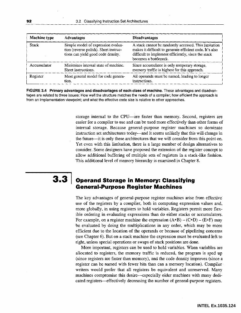
92 3.2 Classifying Instruction Set Architectures
Machine type Advantages Disadvantages
Stack Simple model of expression evalua- A stack cannot be randomly accessed. This limitation tion (reverse polish). Short instruc- makes it difficult to generate efficient code. It's also tions can yield good code density. difficult to implement efficiently, since the stack
becomes a bottleneck.
Accumulator Minimizes internal state of machine. Since accumulator is only temporary storage, Short instructions. memory traffic is highest for this approach.
Register Most general model for code genera- All operands must be named, leading to longer ti on. instructions.
FIGURE 3.4 Primary advantages and disadvantages of each class of machine. These advantages and disadvantages are related to three issues: How well the structure matches the needs of a compiler; how efficient the approach is from an implementation viewpoint; and what the effective code size is relative to other approaches.
storage internal to the CPU-are faster than memory. Second, registers are easier for a compiler to use and can be used more effectively than other forms of internal storage. Because general-purpose register machines so dominate instruction set architectures today-. and it seems unlikely that this will change in the future-it is only these architectures that we will consider from this point on. Yet even with this limitation, there is a large number of design alternatives to consider. Some designers have proposed the extension of the register concept to allow additional buffering of multiple sets of registers in a stack-like fashion. This additional level of memory hierarchy is examined in Chapter 8.
3.3 I Operand Storage in Memory: Classifying General-Purpose Register Machines
The key advantages of general-purpose register machines arise from effective· use of the registers by a compiler, both in computing expression values and, more globally, in using registers to hold variables. Registers permit more flexible ordering in evaluating expressions than do either stacks or accumulators. For example, on a register machine the expression (A*B) - (C*D)- (E*F) may be evaluated by doing the multiplications in any order, which may be more efficient due to the location of the operands or because of pipelining concerns (see Chapter 6). But on a stack machine the expression must be evaluated left to right, unless special operations or swaps of stack positions are done.
More important, registers can be used to hold variables. When variables are allocated to registers, the memory traffic is reduced, the program is sped up (since registers are faster than memory), and the code density improves (since a register can be named with fewer bits than can a memory location). Compiler writers would prefer that all registers be equivalent and unreserved. Many machines compromise this desire-especially older machines with many dedicated registers-effectively decreasing the number of general-purpose registers.
INTEL Ex.1035.124

Number of memory addresses per typical
ALU instruction
0
1
2
3
Instruction Set Design: Alternatives and Principles 93
If the number of truly general-purpose registers is too small, trying to allocate variables to registers will not be profitable. Instead, the compiler will reserve all the uncommitted registers for use in expression evaluation.
How many registers are sufficient? The answer of course depends on how they are used by the compiler. Most compilers reserve some registers for expression evaluation, use some for parameter passing, and allow the remainder to be allocated to hold variables. To understand how many registers are sufficient, we really need to examine what variables can be allocated to registers and the allocation algorithm used. We deal with these in our discussion of compilers in Section 3.7 and examine measurements of register usage in that section.
There are two major instruction set characteristics that divide general-purpose register, or GP R, architectures. Both characteristics concern the nature of operands for a typical arithmetic or logical instruction, or ALU instruction. The first concerns whether an ALU instruction has two or three operands. In the three-operand format, the instruction contains a result and two source operands. In the two-operand format, one of the operands is both a source and a destination for the operation. The second distinction among GPR architectures concerns how many of the operands may be memory addresses in ALU instructions. The number of memory operands supported by a typical ALU instruction may vary from none to three. All possible combinations of these two attributes are shown in Figure 3.5, with examples of machines. While there are seven possible combinations, three serve to classify nearly all existing machines: register-register (also called load/store), register-memory, and memory-memory.
The advantages and disadvantages of each of these alternatives are shown in Figure 3.6 (page 94). Of course, these advantages and disadvantages are not absolutes. A GPR machine with memory-memory operations can easily be subsetted by the compiler and used as a register-register machine. The
Maximum number of Examples operands allowed for a typical ALU instruction
2 IBM RT-PC
3 SPARC, MIPS, HP Precision Architecture
2 PDP-10, Motorola 68000, IBM 360
3 Part of IBM 360 (RS instructions)
2 PDP-11, National 32x32, part of IBM 360 (SS instructions)
3
3 VAX (also has two-operand formats)
FIGURE 3.5 Possible combinations of memory operands and total operands per ALU instruction with examples of machines. Machines with no memory reference per ALU instruction are called load/store or register-register
. machines. Instructions with multiple memory operands per typical ALU instruction are called register-memory or memorymemory, according to whether they have one or more than one memory operand.
INTEL Ex.1035.125

94 3.3 Operand Storage in Memory: Classifying General-Purpose Register Machines
Type Advantages Disadvantages
Register- Simple, fixed-length instruction encoding. Higher instruction count than architectures with register Simple code generation model. Instructions take memory references in instructions. Some
(0,3) similar numbers of clocks to execute (see instructions are short and bit encoding may be Chapter 6). wasteful.
Register- Data can be accessed without loading first. Operands are not equivalent since a source memory Instruction format tends to be easy to encode operand in a binary operation is destroyed.
(1,2) and yields good density. Encoding a register number and a memory
address in each instruction may restrict the number of registers. Clocks per instruction varies by operand location.
Memory- Most compact. Doesn't waste registers for Large variation in instruction size, especially for memory temporaries. three-operand instructions. Also, large variation in
(3,3) work per instruction. Memory accesses create memory bottleneck.
FIGURE 3.6 Advantages and disadvantages of the three most common types of general-purpose register machines. The notation (m, n) means m memory operands and n total operands. In general, machines with fewer alternatives make the compiler's task simpler since there are fewer decisions for the compiler to make. Machines with a wide variety of flexible instruction formats reduce the number of bits required to encode the program. A machine that uses a small number of bits to encode the program is said to have good instruction density-a smaller number of bits do as much work as a larger number on a different architecture. The number of registers also affects the instruction size.
advantages and disadvantages listed in the figure deal primarily with the impact both on the compiler and on the implementation. These advantages and disadvantages are qualitative and their actual impact depends on the compiler and implementation strategy. One of the most pervasive architectural impacts is on instruction encoding and the number of instructions needed to perform a task. In other chapters, we will see the impact of these architectural alternatives on various implementation approaches.
3.4 I Memory Addressing
Independent of whether the architecture is register-register (also called load! store) or allows any operand to be a memory reference, it must define how memory addresses are interpreted and how they are specified. We will deal with these two topics in this section. The measurements presented here are largely, but not completely, machine independent. In some cases the measurements are significantly affected by the compiler technology. These measurements have been made using an optimizing compiler since compiler technology is playing an increasing role. The measurements will probably reflect what we will be seeing in the future rather than what has been so in the past.
INTEL Ex.1035.126

Instruction Set Design: Alternatives and Principles 95
Interpreting Memory Addresses
How is a memory address interpreted? That is, what object is accessed as a function of the address and the length? All the machines discussed in this and the next chapter are byte addressed and provide access for bytes (8 bits), halfwords (16 bits), and words (32 bits). Most of the machines also provide access for doublewords (64 bits).
There are two different conventions for ordering the bytes within a word, as shown in Figure 3. 7. Little Endian byte order puts the byte whose address is "x ... xOO" at the least significant position in the word (the little end). Big Endian byte order puts the byte whose address is "x ... xOO" at the most significant position in the word (the big end). In Big Endian addressing, the address of a datum is the address of the most significant byte; while in Little Endian, the address of a datum is the least significant byte. When operating within one machine, the byte order is often unnoticeable-only programs that access the same locations as both words and bytes can notice the difference. However, byte order is a problem when exchanging data among machines with different orderings. (The byte orders used by a number of different machines are listed inside the front cover.)
Word address
0
4
Little Endian
Word address
0
4
Big Endian
FIGURE 3.7 The two different conventions for ordering bytes within a word. The names "Big Endian" and "Little Endian" come from a famous paper by Cohen [1981). The paper draws an analogy between the argument over which end to number the bytes from and the argument in Gulliver's Travels over which end of an egg to open. The DEC PDP-11 /VAX and Intel 80x86 follow the Little Endian model, while the IBM 360/370 and Motorola 680x0, and others follow the Big Endian model. This numbering applies to bit positions as well, though only a few architectures supply instructions to access bits by their numbered position.
In some machines, accesses to objects larger than a byte must be aligned. An access to an object of size s bytes at byte address A is aligned if A mod s = 0. Figure 3.8 shows the addresses at which an access is aligned or misaligned.
INTEL Ex.1035.127

96 3.4 Memory Addressing
Object addressed Aligned at byte offsets Misaligned at byte offsets
byte O,l,2,3,4,5,6,7 (never)
halfword 0,2,4,6 1,3,5,7
word 0,4 1,2,3,5,6,7
doubleword 0 1,2,3,4,5,6,7
FIGURE 3.8 Aligned and misaligned accesses of objects. The byte offsets are specified for the low-order three bits of the address.
Why would someone design a machine with alignment restrictions? Misalignment causes hardware complications, since the memory is typically aligned on a word boundary. A misaligned memory access will, therefore, take multiple aligned memory references. Figure 3.9 shows what happens when an access occurs to a misaligned word in a system with a 32-bit-wide bus to memory: Two accesses are required to get the word. Thus, even in machines that allow misaligned access, programs with aligned accesses run faster.
Misaligned word reference
32 32 32 bits ___ ....._ _____ ,__ ____ ....._ __ _
32
To CPU
FIGURE 3.9 A word reference is made to a halfword (16-bit) boundary in a memory system that has a 32-bit access path. The CPU or memory system has to perform two separate accesses to get the upper and lower halfword. The two halfwords are then merged to obtain the entire word. With memory organized as independent byte-wide modules it is possible to access only the needed data, but this requires more complex control to supply a different address to each module to select the proper byte.
Even if data is aligned, supporting byte and halfword accesses requires an alignment network to align bytes and halfwords in registers. Depending on the instruction, the machine may also need to sign extend the quantity. On some machines a byte or halfword does not affect the upper portion of a register. For stores only the affected bytes in memory may be altered. Figure 3.10 shows the
INTEL Ex.1035.128

Instruction Set Design: Alternatives and Principles 97
alignment network for loading or storing a byte from a word in memory into a register. While all the machines discussed in this chapter and the next permit byte and halfword accesses to memory, only the VAX and the Intel 8086 support ALU operations on register operands with a size shorter than a word.
Byte in register
0 2 I 3 I Alignment network ;/]
0 2 I 3 I Word in memory
FIGURE 3.10 · The alignment network to load or store a byte. The memory system is assumed to be 32 bits wide, and four alignment paths are required for bytes. Accessing aligned halfwords would require two additional paths to move either byte 0 or byte 2 in memory to byte 2 in the register. A 64-bit memory system would require twice as many alignment paths for bytes and halfwords, as well as two 32-bit alignment paths for word accesses. The alignment network only positions the bytes for a store-additional control signals are used to ensure that only the correct byte positions are written in memory. Rather than an alignment network, some machines use a shifter and shift the data only in those cases where alignment is required. This makes the access of a nonword object considerably slower, but eliminating the alignment network speeds up the more common case of accessing a word.
Addressing Modes
We now know what bytes to access in memory given an address. In this section we will look at addressing modes-how architectures specify the address of an object they will access. In GPR machines, an addressing mode can specify a constant, a register, or a location in memory. When a memory location is used, the actual memory address specified by the addressing mode is called the effective address.
Figure 3 .11 shows all the data addressing modes that arise in the machines discussed in the following chapter. Immediates or literals are usually considered a memory addressing mode (even though the value they access is in the instruction stream), while registers are often separated. We have kept addressing modes that depend on the program counter, called PC-relative addressing, separate. PC-relative addressing is used primarily for specifying code addresses in control
INTEL Ex.1035.129

98
Addressing mode
Register
Immediate or literal
Displacement or based
Register defer-red or indirect
Indexed
Direct or absolute
Memory indi-rector mem-ory deferred
Auto-increment
Auto-decrement
Scaled or index
3.4 Memory Addressing
transfer instructions. The use of PC-relative addressing in control instructions is discussed in Section 3 .5.
Figure 3 .11 shows the most common names for the addressing modes, though the names differ among architectures. In this figure and throughout the book, we will use an extension of the C programming language as a hardware description notation. In this figure, only two non-C features are used. First, the left arrow ( ~) is used for assignment. Second, the array M is used as the name for memory.
Example instruction Meaning When used
Add R4,R3 R4f-R4+R3 When a value is in a register.
Add R4,#3 R4f-R4+3 For constants. In some machines, literal and immediate are two different addressing modes.
Add R4,100(Rl) R4f-R4+M [ lOO+Rl] Accessing local variables.
Add R4, (Rl) R4f-R4+M [Rl] Accessing using a pointer or a computed address.
Add R3, (Rl + R2) R3f-R3+M [Rl+R2] Sometimes useful in array ad-dressing-Rl=base of array; R2=index amount.
Add Rl I ( 1001) Rlf-Rl+M[lOOl] Sometimes useful for accessing static data; address constant may need to be large.
Add Rl,@(R3) Rlf-Rl +M [M [R3]] If R3 is the address of a pointer p, then mode yields *P·
Add Rl, (R2)+ Rlf-Rl +M [R2] Useful for stepping through arrays within a loop. R2 points to start of
R2f-R2+d array; each reference increments R2 by size of an element, d.
Add Rl, - (R2) R2f-R2-d Same use as autoincrement. Autoincrement/decrement can also be
Rlf-Rl +M [R2] used to implement a stack as push and pop.
Add Rl,100(R2) [R3] Rlf- Used to index arrays. May be applied Rl+M[100+R2+R3*d] to any base addressing mode in some
machines.
FIGURE 3.11 Selection of addressing modes with examples, meaning, and usage. The extensions to C used in the hardware descriptions are defined above. In autoincrement/decrement and scaled or index addressing modes, the variable d designates the size of the data item being accessed (i.e., whether the instruction is accessing 1, 2, 4, or 8 bytes); this means that these addressing modes are only useful when the elements being accessed are adjacent in memory. In our measurements, we use the first name shown for each mode. A few machines, such as the VAX, encode some of these addressing modes as PC-relative.
INTEL Ex.1035.130

l
Instruction Set Design: Alternatives and Principles 99
Thus, M [ Rl J refers to the contents of the memory location whose address is given by the contents of RI. Later, we will introduce extensions for accessing and transferring data smaller than a word.
Addressing modes have the ability to significantly reduce instruction counts; they also add to the complexity of building a machine. Thus, the usage of various addressing modes is quite important in helping the architect choose what to include. While many measurements of addressing mode usage are machine dependent, others are largely independent of the machine architecture. Some of the more important machine-independent measurements will be examined in this chapter. But, before we look at this type of measurement, let's look at how often these various memory addressing modes are used.
Figure 3.12 shows the results of measuring addressing mode usage patterns in our benchmarks-Gnu C Compiler (GCC), Spice, and TeX-on the VAX, which supports all the modes shown in Figure 3.11. We will look at further measurements of addressing mode usage on the VAX in the next chapter.
As Figure 3.12 shows, immediate and displacement addressing dominate addressing mode usage. Let's look at some properties of these two heavily used modes.
TeX
Memory indirect Spice 6% GCC
TeX
Scaled Spice 16% GCC 6%
TeX 24% Register deferred Spice
GCC 11%
TeX 43%
Immediate Spice 17% GCC 39%
TeX 32%
Displacement Spice 55% GCC 40%
0% 10% 20% 30% 40% 50% 60%
Frequency of the addressing mode
FIGURE 3.12 Summary of use of memory addressing modes (including immediates). The data were taken on a VAX using our three benchmark programs. Only the addressing modes with an average frequency of over 1 % are shown. The PC-relative addressing modes, which are used almost exclusively for branches, are not included. Displacement mode includes all displacement lengths (8-, 16-, and 32-bit). Register modes, which are not counted, account for one-half of the operand references, while memory addressing modes (including immediate) account for the other half. The memory indirect mode on the VAX can use displacement, autoincrement, or autodecrement to form the initial memory address; in these programs, almost all the memory indirect references use displacement mode as the base. Of course, the compiler affects what addressing modes are used; we discuss this further in Section 3.7. These major addressing modes account for all but a few percent (0% to 3%) of the memory-accesses.
INTEL Ex.1035.131

100 3.4 Memory Addressing
Displacement or Based Addressing Mode
The major question that arises for a displacement-style addressing mode is that of the range of displacements used. Based on the use of various displacement sizes, a decision of what sizes to support can be made. Choosing the displacement field sizes is important because they directly affect the instruction length. Measurements taken on the data access on a load/store architecture using our three benchmark programs are shown in Figure 3.13. We will look atbranch offsets in the next section-data accessing patterns and branches are so different, little is gained by combining them.
30%
25%
0 2 3 4 5 6 7 8 9 10 11 12 13 14 15
Number of bits needed for a displacement value
j -o- TeX -+- Spice -x- GCC.
FIGURE 3.13 Displacement values are widely distributed. Though there is a large number of small values, there is also a fair number of large values. The wide distribution of displacement values is due to multiple storage areas for variables and different displacements used to access them. The different storage areas and their access patterns are discussed further in Section 3. 7. The chart shows only the magnitude of the displacement and not the sign, which is heavily affected by the storage layout. The entry corresponding to 0 on the x axis shows the percentage of displacements of value 0. The vast majority of the displacements are positive, but a majority of the largest displacements (14+ bits) are negative. Again, this is due to the overall addressing scheme used by the compiler and might change with a different compilation scheme. Since this data was collected on a machine with 16-bit displacements, it cannot tell us anything about accesses that might want to use a longer displacement. Such accesses are broken into two separate instructions-the first of which loads the upper 16 bits of a base register. By counting the frequency of these "load immediate" instructions, which have limited use for other purposes, we can bound the number of accesses with displacements potentially larger than 16 bits. Such an analysis indicates GCC, Spice, and TeX may actually require a displacement longer than 16 bits for up to 5%, 13%, and 27% of the memory references, respectively. Furthermore, if the displacement is larger than 15 bits, it is likely to be quite a bit larger since most constants being loaded are large, as shown in Figure 3.15 (page 102).To evaluate the choice of displacement length, we might also want to examine a cumulative distribution, as shown in Exercise 3.3 (see Figure 3.35 on page 133).
INTEL Ex.1035.132
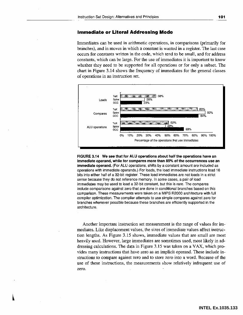
Instruction Set Design: Alternatives and Principles 101
Immediate or Literal Addressing Mode
lmmediates can be used in arithmetic operations, in comparisons (primarily for branches), and in moves in which a constant is wanted in a register. The last case occurs for constants written in the code, which tend to be small, and for address constants, which can be large. For the use of immediates it is important to know whether they need to be supported for all operations or for only a subset. The chart in Figure 3.14 shows the frequency of immediates for the general classes of operations in an instruction set.
TeX
Loads Spice GCC
TeX
Compares Spice GCC
ALU operations
38% 26%
23%
83% 92%
84%
0% 10% 20% 30% 40% 50% 60% 70% 80% 90% 100%
Percentage of the operations that use immediates
FIGURE 3.14 We see that for ALU operations about half the operations have an immediate operand, while for compares more than 85% of the occurrences use an immediate operand. (For ALU operations, shifts by a constant amount are included as operations with immediate operands.) For loads, the load immediate instructions load 16 bits into either half of a 32-bit register. These load immediates are not loads in a strict sense because they do not reference memory. In some cases, a pair of load immediates may be used to load a 32-bit constant, but this is rare. The compares include comparisons against zero that are done in conditional branches based on this comparison. These measurements were taken on a MIPS R2000 architecture with full compiler optimization. The compiler attempts to use simple compares against zero for branches whenever possible because these branches are efficiently supported in the architecture.
Another important instruction set measurement is the range of values for immediates. Like displacement values, the sizes of immediate values affect instruction lengths. As Figure 3.15 shows, immediate values that are small are most heavily used. However, large immediates are sometimes used, most likely in addressing calculations. The data in Figure 3.15 was taken on a VAX, which provides many instructions that have zero as an implicit operand. These include instructions to compare against zero and to store zero into a word. Because of the use of these instructions, the measurements show relatively infrequent use of zero.
INTEL Ex.1035.133

102 3.4 Memory Addressing
0 4 8 12 16 20 24 28 32 Number of bits needed for an immediate value
-+- GCC -a- Spice -x-TeX
FIGURE 3.15 The distribution of immediate values is shown. The x axis shows the number of bits needed to represent the magnitude of an immediate value-a means the immediate field value was 0. The vast majority of the immediate values are positive: Overall, less than 6% of the immediates are negative.These measurements were taken on a VAX, which supports a full range of immediates and sizes as operands to any instruction. The measured programs are the standard set-GCC, Spice, and TeX.
Encoding of Addressing Modes
How the addressing modes of operands are encoded depends on the range of addressing modes and the degree of independence between opcodes and modes. For a small number of addressing modes or opcode/addressing mode combinations, the addressing mode can be encoded in the opcode. This works for the IBM 360 with only five addressing modes and most operations offered in only one or two modes. For a large number of combinations, typically a separate address specifier is needed for each operand. The address specifier tells what addressing mode the operand is using. In Chapter 4, we will see how these two types of encodings are used in several real instruction formats.
When encoding the instructions, the number of registers and the number of addressing modes both have a significant impact on the size of instructions. This is because the addressing mode field and the register field may appear many times in a single instruction. In fact, for most instructions many more bits are consumed encoding addressing modes and register fields than in specifying the opcode. The architect must balance several competing forces when encoding the instruction set:
1. The desire to have as many registers and addressing modes as possible.
INTEL Ex.1035.134

3.s 1
Operator type
Arithmetic and logical
Data transfer
Control
System
Floating point
Decimal
String
Instruction Set Design: Alternatives and Principles 103
2. The impact of the size of the register and addressing mode fields on the average instruction size and hence on the average program size.
3. A desire to have instructions encode into lengths that will be easy to handle in the implementation. As a minimum, the architect wants instructions to be in multiples of bytes, rather than an arbitrary length. Many architects have chosen to use a fixed-length instruction to gain implementation benefits while sacrificing average code size.
S!nce the addressing modes and register fields make up such a large percentage of the instruction bits, their encoding will significantly affect how easy it is for an implementation to decode the instructions. The importance of having easily decoded instructions is discussed in Chapters 5 and 6.
Operations in the Instruction Set
The operators supported by most instruction set architectures can be categorized, as in Figure 3.16. In Section 3.8, we look at the use of operations in a general fashion (e.g. memory references, ALU operations, and branches). In Chapter 4, we will examine the use of various instruction operations in detail for four different architectures. Because the instructions used to implement control flow are largely independent of other instruction set choices and because the measurements of branch and jump behavior are also fairly independent of other measurements, we examine the use of control-flow instructions next.
Examples
Integer arithmetic and logical operations: add, and, subtract, or
Loads/stores (move instructions on machines with memory addressing)
Branch, jump, procedure call and return, traps
Operating system call, virtual memory management instructions
Floating-point operations: add, multiply
Decimal add, decimal multiply, decimal-to-character conversions
String move, string compare, string search
FIGURE 3.16 Categories of instruction operators and examples of each. All machines generally provide a full set of operations for the first three categories. The support for system functions in the instruction set varies widely among architectures, but all machines must have some instruction support for basic system functions. The amount of support in the instruction set for the last three categories may vary from none to an extensive set of special instructions. Floatingpoint instructions will be provided in any machine that is intended for use in an application that makes much use of floating point. These instructions are sometimes part of an optional instruction set. Decimal and string instructions are sometimes primitives, as in the VAX or the IBM 360, or may be synthesized by the compiler from simpler instructions. Examples of instruction sets appear in Appendix 8, while Appendix C contains measurements of typical usage. We will examine four different instruction sets and their usage in detail in Chapter 4.
INTEL Ex.1035.135

104 3.5 Operatidns in the Instruction Set
Instructions for Control Flow
As Figure 3 .17 shows, there is no consistent terminology for instructions that change the flow of control. Until the IBM 7030, control-flow instructions were typically called transfers. Beginning with the 7030, the name branch began to be used. Later, machines introduced additional names. Throughout this book we will use jump when the change in control is unconditional and branch when the change is tonditional.
Machine Year "Branch" "Jump"
IBM7030 1960 All control transfers-addressing is PC-relative
IBM 360/370 1965 All control transfers-no PC-relative
DEC PDP-11 1970 PC-relative only, All addressing modes; conditional and unconditional only unconditional
;
Intel 8086 1978 All transfers are jumps; conditional jumps are PC-relative only
DEC VAX 1978 Same as PDP-11 Same as PDP-11
MIPS R2000 1986 Conditional control Unconditional jumps and transfer, always PC- call instructions relative
FIGURE 3.17 Machines, dates, and the names associated with control transfers in their architectures. These names vary widely based on whether the transfer is conditional or unconditional and on whether it is PC-relative or not. The VAX, PDP-11, and MIPS R2000 architectures allow only PC-relative addressing for branches.
We can distinguish four different types of control-flow change:
1. Conditional branches
2. Jumps
3. Procedure calls
4. Procedure returns
We want to know the relative frequency of these events, as each event is different, may use different instructions, and may have different behavior. The frequencies of these control-flow instructions for a load/store machine running 04r benchmarks is shown in Figure 3.18.
The destination address of a branch must always be specified. This destination is specified explicitly in the instruction in the vast majority of cases-pro-
INTEL Ex.1035.136

Instruction Set Design: Alternatives and Principles 105
cedure return being the major exc;:eption-since for return the target is not known at compile time. The most common way to specify the destination is to supply a displacement that is added to the program counter, or PC. Branches of this sort are called PC-relative branches. PC-relative branches are advantageous because the branch target is often near the current instruction, and specifying the position relative to the current PC requires fewer bits. Using PC-relative addressing also permits the code to run independent of where it is loaded. This property, called position-independence, can eliminate some work when the program is linked and is also useful in programs linked during execution.
Call/return
Jump
Conditional
TeX 16% Spice 13% GCC 10%
TeX " 18% Spice 12% GCC 12%
TeX 66%
Spice·················75% GCC 78%
0% 10% 20% 30% 40% 50% 60% 70% 80% 90%
Frequency of a branch of this type
FIGURE 3.18 Breakdown of branches into three classes. Each branch is counted in one of three bars. Conditional branches clearly dominate. On average 90% of the jumps are PC-relative.
To implement returns and indirect branches in which the target is not known at compile time, a method other than PC-relative addressing is required. Here, there must be a way to specify the target dynamically, so that it can change at
· run-time. This may be as simple as naming a register that contains the target address. Alternatively, the branch may permit any addressing mode to be used to supply the target address.
A key question concerns how far branch targets are from branches. Knowing the distribution of these displacements will help in choosing what branch offsets to support and thus will affect the instruction length and encoding. Figure 3.19 (page 106) shows the distribution of displacements for PC-relative branches in instructions. About 75% of the branches are in the forward direction.
Since most changes in control flow are branches, deciding how to specify the branch condition is important. The three primary techniques. in use and their advantages and disadvantages are shown in Figure 3.20 (page 106).
INTEL Ex.1035.137

106
Name
Condition code (CC)
Condition register
Compare and branch
3.5 Operations in the Instruction Set
30%
25%
20%
15%
10%
5%
0% 2 3 4 5 6 7 8 9 10 11 12 13 14
Log2 of the branch distance in instructions
....... Tex o Spice • GCC I FIGURE 3.19 Branch distances in terms of number of instructions between the target and the branch instruction.The most frequent branches in Spice are to targets that are 8 to 15 instructions away (24
). The weighted-arithmetic-mean branch target distance is 86 instructions (2\ This tells us that short displacement fields often suffice for branches and that the designer can gain some encoding density by having a shorter instruction with a smaller branch displacement. These measurements were taken on a load/store machine (MIPS R2000 architecture). An architecture that requires fewer instructions for the same program, such as a VAX, would have shorter branch distances. Similarly, the number of bits needed for the displacement may change if the machine allows instructions to be arbitrarily aligned. A cumulative distribution of this branch displacement data is shown in Exercise 3.3 (see Figure 3.35 on page 133).
How condition is tested Advantages Disadvantages
Special bits are set by ALU Sometimes condition is CC is extra state. Condition codes operations, possibly under set for free. constrain t.he ordering of instructions program control. since they pass information from one
instruction to a branch.
Set arbitrary register with the Simple. Uses up a register. result of a comparison.
Compare is part of the branch. One instruction rather May be too much work per Often compare is limited to subset. than two for a branch. instruction.
FIGURE 3.20 The major methods for evaluating branch conditions, their advantages, and disadvantages. Although condition codes can be set by ALU operations that are needed for other purposes, measurements on programs show that this rarely happens. The major implementation problems with condition codes arise when the condition code is set by a large or haphazardly chosen subset of the instructions, rather than being controlled by a bit in the instruction. Machines with compare and branch often limit the set of compares and use a condition register for more complex compares. Often, different techniques are used for branches based on floating-point comparison versus those based on integer comparison. This is reasonable since the number of branches that depend on floating-point comparisons is much smaller than the number depending on integer comparisons.
INTEL Ex.1035.138

·Instruction Set Design: Alternatives and Principles 107
One of the most noticeable properties of branches is that a large number of the comparisons are simple equality or inequality tests, and a large number are comparisons with zero. Thus, some architectures choose to treat these comparisons as special cases, especially if a compare and branch instruction is being used. Figure 3.21 shows the frequency of different comparisons used for conditional branching. The data in Figure 3 .14 said that a large percentage of the branches had an immediate operand (86% ), and while not shown, 0 was the most heavily used immediate (83% of the immediates in branches). When we combine this with the data in Figure 3.21 we can see that a significant percentage (over 50%) of the compares in branches are simple tests for equality with zero.
LT/GE
GT/LE
EQ/NE
TeX 25% Spice GCC 11%
TeX Spice 25% GCC
TeX ···········••R.z72% _Spice 75% GCC················-89%
0% 10% 20% 30% 40% 50% 60% 70% 80% 90% 100%
Frequency of comparison types in branches
FIGURE 3.21 Frequency of different types of compares in conditional branches. This includes both the integer and floating-point compares in branches. Floating-point comparisons constitute 13% of the branch comparisons in Spice. Remember that earlier data in Figures 3.14 indicate that most comparisons are against an immediate operand. This immediate value is usually 0 (83% of the time).
Program Percentage of Percentage taken Percentage of all backward branches control instructions branches that actually branch
GCC 26% 54% 63%
Spice 31% 51% 63%
TeX 17% 54% 70%
Average 25% 53% 65%
FIGURE 3.22 Branch direction, branch-taken frequency, and frequency that the PC is changed. The first column shows what percentage of all branches (both taken and untaken) are backward-going. The second column shows what percentage of all branches (remember that a branch is always conditional) are taken. The final column shows what_ percentage of all control-flow instructions actually cause a nonsequential transfer in the flow. This last column is computed by combining data from the second column and the data in Figure 3.18 (page 105).
INTEL Ex.1035.139

108
Example
Answer
· 3.5 Operations in the Instruction Set
We will say that a branch is taken if the condition tested by the branch is true and the next instruction to be executed is the target of the branch. All jumps, therefore, are taken. Figure 3.22 shows the branch-direction distribution, the frequency of taken (conditional) branches, and the percentage of control-flow instructions that change the PC. Most backward-going branches are loop branches, and typically loop branches are taken with about 90% probability.
Many programs have.a higher percentage of loop branches, thus boosting the frequency of taken branches over 60%. Overall, branch behavior is applicationdependent and sometimes compiler-dependent. Compiler dependencies arise because of changes to the control flow made by optimizing compilers to improve the execution time of loops.
Assuming that 90% of the backward-going branches are taken, find the probability that a forward-going branch is taken using the averaged data in Figure 3.22.
The average frequency of taken branches is the sum of the backward-taken and forward-taken times their respective frequencies:
% taken branches = (%taken backward*% backward)+ (%taken forward*% forward)
53% = (90% * 25%) +(%taken forward* 75%)
53%-22.5% % taken forward = -----75%
% taken forward = 40.7%
It is not unusual to see the majority of forward branches be untaken. The behavior of forward-going branches often varies among programs.
Procedure calls and returns include control transfer and possibly some state saving; at a minimum the return address must be saved somewhere. Some architectures provide a mechanism to save the registers, while others require the compiler to generate instructions. There are two basic conventions in use to save registers. Caller-saving means that the calling procedure must save the registers that it wants preserved for access after the call. Callee-saving means that the called procedure must save the registers it wants to use. There are times when caller save must be used due to access patterns to globally visible variables in two different procedures. For example, suppose we have a procedure Pl that calls procedure P2, and both procedures manipulate the global variable x. If Pl had allocated x to a register it must be sure to save x to a location known by P2 before the call to P2. A compiler's ability to discover when a called procedure
INTEL Ex.1035.140

Instruction Set Design: Alternatives and Principles 109
may access register-allocated quantities is complicated by the possibility of separate compilation, and situations where P2 may not touch x, but P2 can call another procedure, P3, that may access x. Because of these complications, most compilers will conservatively caller save any variable that may be accessed during a call.
In the cases where either convention could be used, some will be more optimal with callee-save and some will be more optimal with caller-save. As a
t'fesult, the most sophisticated compilers use a combination of the two mechanisms, and the register allocator may choose which register to use for a variable based on the convention. Later in this chapter we will examine how well more sophisticated instructions match the needs of the compiler for this function, and in Chapter 8 we will look at hardware buffering schemes for supporting register save and restore.
3.6 I Type and Size of Operands
How is the type of an operand designated? There are two primary alternatives: First, the type of an operand may be designated by encoding it in the opcodethis is the method used most often. Alternatively, the data can be annotated with tags that are interpreted by the hardware. These tags specify the type of the operand, and the operation is chosen accordingly. Machines with tagged data, however, are extremely rare. The Burroughs' architectures are the most extensive example of tagged architectures. Symbolics also built a series of machines that used tagged data items for implementing LISP.
Usually the type of an operand-for example, integer, single-precision floating point, character-effectively gives its size. Common operand types include character (one byte), halfword (16 bits), word (32 bits), single-precision floating point (also one word), and double-precision floating point (two words). Characters are represented as either EBCDIC, used by the IBM mainframe architectures, or ASCII, used by everyone else. Integers are almost universally represented as two's complement binary numbers. Until recently, most computer manufacturers chose their own floating-point representation. However, in the past few years, a standard for floating point, the IEEE standard 754, has become the choice of most new computers. The IEEE floating-point standard is discussed in detail in Appendix A.
Some architectures provide operations on character strings, although such operations are usually quite limited and treat each byte in the string as a single character. Typical operations supported on character strings are comparisons and moves.
For business applications, some architectures support a decimal format, usually called packed decimal. Packed decimal is binary-coded decimal-four bits are used to encode the values 0-9, and two decimal digits are packed into each byte. Numeric character strings are sometimes called unpacked decimal, and
INTEL Ex.1035.141
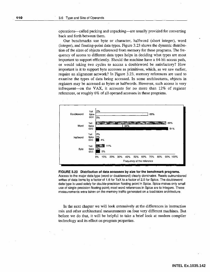
110 3.6 Type and Size of Operands
operations-called packing and unpacking-are usually provided for converting back and forth between them.
Our benchmarks use byte or character, halfword (short integer), word (integer), and floating-point data types. Figure 3.23 shows the dynamic distribution of the sizes of objects referenced from memory for these programs. The frequency of access to different data types helps in deciding what types are most important to support efficiently. Should the machine have a 64-bit access path, or would taking two cycles to access a doubleword be satisfactory? How important is it to support byte accesses as primitives, which, as we saw earlier, require an alignment network? In Figure 3.23, memory references are used to examine the types of data being accessed. In some architectures, objects in registers may be accessed as bytes or halfwords. Howev_yr, such access is very infrequent-on the VAX, it accounts for no more than 12% of register references, or roughly 6% of all operand accesses in these programs.
TeX Doubleword Spice
GCC
TeX Word Spice
GCC
TeX Halfword Spice
GCC
TeX Byte Spice
GCC
0% 66%
0%
89% 34%
91%
11%
0% 10% 20% 30% 40% 50% 60% 70% 80% 90% 100%
Frequency of the reference
FIGURE 3.23 Distribution of data accesses by size for the benchmark programs. Access to the major data type (word or doubleword) clearly dominates. Reads outnumbered writes of data items by a factor of 1.6 for TeX to a factor of 2.5 for Spice. The doubleword data type is used solely for double-precision floating point in Spice. Spice makes only small use of single-precision floating point; most word references in Spice are to integers. These measurements were taken on the memory traffic generated on a load/store architecture.
In the next chapter we will look extensively at the differences in instruction mix and other architectural measurements on four very different machines. But before we do that, it will be helpful to take a brief look at modern compiler technology and its effect on program properties.
INTEL Ex.1035.142

Instruction Set Design: Alternatives and Principles
3. 7 I The Role of High-Level Languages and Compilers
111
Today most programming is done in high-level languages. This means that since most instructions executed are the output of a compiler, an instruction set archit~cture is essentially a compiler target. In earlier times, architectural decisions were often made to ease assembly language programming. Because performance of a computer will be significantly affected by the compiler, understanding compiler technology today is critical to designing and efficiently implementing an instruction set. In earlier days it was popular to try to isolate the compiler technology and its effect on hardware performance from the architecture and its peiformance, just as it was popular to try to separate an architecture from its implementation. This is extremely difficult, if not impossible, with today's compilers and architectures. Architectural choices affect the quality of the code that can be generated for a machine and the complexity of building a good compiler for it. Isolating the compiler from the hardware is likely to be misleading. In this section we will discuss the critical goals in the instruction set primarily from the compiler viewpoint. What features will lead to high-quality code? What makes it easy to write efficient compilers for an architecture?
The Structure of Recent Compilers
To begin, let's look at what optimizing compilers are like today. The structure of recent compilers is shown in Figure 3.24.
A compiler writer's first goal is correctness-all valid programs must be compiled correctly. The second goal is usually speed of the compiled code. Typically, a whole set of other goals follow these first two, including fast compilation, debugging support, and interoperability among languages. Normally, the passes in the compiler transform higher-level, more abstract representations into progressively lower-level representations, eventually reaching the instruction set. This structure helps manage the complexity of the transformations and makes writing a bug-free compiler easier.
The complexity of writing a correct compiler is a major limitation on the amount of optimization that can be done. Although the multiple-pass structure helps reduce compiler complexity, it also means that the compiler must order and perform some transformations be\ore others. In the diagram of the. optimizing compiler in Figure 3.24, we can see that certain high-level optimizations are performed long before it is known what the resulting code will look like in detail. Once such a transformation is made, the compiler can't afford to go back and revisit all steps, possibly undoing transformations. This would be prohibiti_ve, both in compilation time and in complexity. Thus, compilers make assumptions about the ability of later steps to deal with certain problems. For example, compilers usually have to choose which procedure calls to expand inline before they know the exact size of the procedure being called. Compiler writers call this problem the phase-ordering problem.
INTEL Ex.1035.143

112 3.7 The Role of High-Level Languages and Compilers
Dependencies Language dependent; machine independent
Somewhat language dependent, largely machine independent
Small language dependencies; machine dependencies slight (e.g., register counts/types)
Highly machine dependent; language independent
Intermediate representation
Function Transform language to common intermediate form
For example, procedure inlining and loop transformations
Including global and local optimizations + register allocation
Detailed instruction selection and machine-dependent optimizations; may include or be followed by assembler
FIGURE 3.24 Current compilers typically consist of two to four passes, with more highly optimizing compilers having more passes. A pass is simply one phase in which the compiler reads and transforms the entire program. (The term "phase" is often used interchangeably with "pass.") The optimizing passes are designed to be optional and may be skipped when faster compilation is the goal and lower quality code is acceptable. This structure maximizes the probability that a program compiled at various levels of optimization will produce the same output when given the same input. Because the optimizing passes are also separated, multiple languages can use the same optimizing and code-generation passes. Only a new .front end is required for a new language. The highlevel optimization mentioned here, procedure inlining, is also called procedure integration.
How does this ordering of transformations interact with the instruction set architecture? A good example occurs with the optimization called global common subexpression elimination. This optimization finds two instances of an expression that compute the same value and saves the value of the first computation in a temporary. It then uses the temporary value, eliminating the second computation of the expression. For this optimization to be significant, the temporary must be allocated to a register. Otherwise, the cost of storing the temporary in memory and later reloading it may negate the savings gained by not recomputing the expression. There are, in fact, cases where this optimization actually slows down code when the temporary is not register allocated. Phase ordering complicates this problem, because register allocation is typically done near the end of the global optimization pass, just before code generation. Thus, an optimizer that performs this optimization must assume that the register allocator will allocate the temporary to a register.
INTEL Ex.1035.144

Instruction Set Design: Alternatives and Principles 113
Because of the central role that register allocation plays, both in speeding up the code and in making other optimizations useful, it is one of the most important-if not the most important-optimizations. Recent register allocation algorithms are based on a technique called graph coloring. The basic idea behind graph coloring is to construct a graph representing the possible candidates for allocation to a register and then to use the graph to allocate registers. As shown in Figure 3.25, each candidate for a register corresponds to a node in the graph, called an interference graph. The arcs between the nodes show where the ranges of usage for variables (called live ranges) overlap. The compiler then tries to color the graph using a number of colors equal to the number of registers available for allocation. In a graph coloring, no adjacent nodes may have the same color. This restriction is equivalent to saying that no two variables with overlapping uses may be allocated to the same register. However, nodes that are not connected by an arc may have the same color, allowing variables whose uses do not overlap to use the same register. Thus, a coloring of the graph corresponds to an allocation of the active variables to registers. For example, the four nodes in Figure 3.25 can be colored with two colors, meaning the code only needs two registers for allocation. Although the problem of coloring a graph is NP-complete, there are heuristic algorithms that work well in practice.
a. Program fragment
A= B=
... 8 ... C= ... A .. . D= .. . ... D .. . ... c .. .
c. Colored graph
b. Interference graph
d. Registerallocated code
R1 = R2=
... R2 ... R2= ... R1 .. . R1= .. . ... R1 .. . ... R2 .. .
FIGURE 3.25 Graph coloring is used to allocate registers by constructing an interference graph that is colored heuristically using a number of colors corresponding to the register count. Part b shows the interference graph corresponding to the code fragment shown in part a. Each variable corresponds to a node, and the arcs show the overlap of the active ranges of the variables. The graph can be colored with two colors, as shown in part c, and this corresponds to the register allocation of part d.
INTEL Ex.1035.145

114
Optimization name
High-level
Procedure integration
Local
Common subexpression elimination
Constant propagation
Stack height reduction
Global
.Global common subexpression elimination
Copy propagation
·Code motion
Induction variable elimina-ti on
Machine-dependent
Strength reduction
Pipeline scheduling
Branch offset optimization
3.7 The Role of High-Level Languages and Compilers
Graph coloring works best when there are at least 16 (and preferably more) general-purpose registers available for global allocation for integer variables and additional registers for floating point. Unfortunately, graph coloring does not work very well when the number of registers is small because the heuristic algorithms for coloring the graph are likely to fail. The emphasis in the approach is to achieve 100% allocation of active variables.
Optimizations performed by modern compilers can be classified by the style of the transformation, as follows:
1. High-level optimizations-often done on the source with output fed to later optimization passes.
Explanation Percent of the total number of optimizing transforms
At or near the source level; machine-independent
Replace procedure call by procedure body N.M.
Within straightline code
Replace two instances of the same computation by single copy 18%
Replace all instances of a variable that is assigned a constant with the 22% constant
Rearrange expression tree to minimize resources needed for expression N.M. evaluation
Across a branch
Same as local, b,ut this version crosses branches 13%
Replace all instances of a variable A that has been assigned X (i.e., A=X) 11% withX
Remove code from a loop that computes same value each iteration of the loop 16%
Simplify/eliminate array-addressing calculations within loops 2%
Depends on machine knowledge
Many examples, such as replace multiply by a constant with adds and shifts N.M.
Reorder instructions to improve pipeline performance N.M.
Choose the shortest branch displacement that reaches target N.M.
FIGURE 3.26 Major types of optimizations and examples in each class. The third column lists the static frequency with which some of the common optimizations are applied in a set of 12 small FORTRAN and Pascal programs. The percentage is the portion of the static optimizations that are of the specified type. These data tell us about the relative frequency of occurrence of various optimizations. There are nine local and global optimizations done by the compiler included in the measurement. Six of these optimizations are covered in the figure, and the remaining three account for 18% of the total static occurrences. The abbreviation "N.M." means that the number of occurrences of that optimization was not measured. Machine-dependent optimizations are usually done in a code generator, and none of those were measured in this experiment. The data are from Chow [1983], and were collected using the Stanford UCODE compiler.
INTEL Ex.1035.146

Instruction Set Design: Alternatives and Principles 115
2. Local optimizations-optimize code only within a straightline code fragment (called a basic block by compiler people).
3. Global optimizations-extend the local optimizations across branches and introduce a set of transformations aimed at optimizing loops.
4. Register allocation.
5. Machine-dependent optimizations-attempt to take advantage of specific architectural knowledge.
It is sometimes difficult to separate some of the simpler optimizations-local and machine-dependent optimizations-from transformations done in the code generator. Examples of typical optimizations are given in Figure 3.26. The last column of Figure 3.26 indicates the frequency with which the listed optimizing
. transforms. were applied to the source program. Data on the effect of various optimizations on program run-time are shown in Figure 3.27. The data in Figure 3.27 demonstrate the importance of register allocation, which adds the largest single improvement. We will look at the overall effect of optimization on our three benchmarks later in this section.
Optimizations performed Percent faster
Procedure integration only 10%
Local optimizations only 5%
Local optimizations + register allocation 26%
Global and local optimizations 14%
Local and global optimizations + register allocation 63%
Local and global optimizations + procedure integration + 81% register allocation
FIGURE 3.27 Performance effects of various levels of optimization. Performance gains are shown as what percent faster the optimized programs were compared to the unoptimized programs. When register allocation is turned off, data are loaded into, or stored from, the registers on every individual use. These measurements are also from Chow [1983] and are for 12 small FORTRAN and Pascal programs.
The Impact of Compiler Technology on the Architect's Decisions
The interaction of compilers and high-level languages significantly affects how programs use an instruction set. To better understand this interaction, three important questions to ask are:
1. How are variables allocated and addressed? How many registers are needed to allocate variables appropriately?
2. What is the impact of optimization techniques on instruction mixes?
INTEL Ex.1035.147

116 3.7 The Role of High-Level Languages and Compilers
3. What control structures are used and with what frequency?
To address the first questions, we must look at the three separate areas in which current high-level languages allocate their data:
• The stack-used to allocate local variables. The stack is grown and shrunk on procedure call or return; respectively. Objects on the stack are addressed relative to the stack pointer and are primarily scalars (single variables) rather than arrays. The stack is used for activation records, not as a stack for evaluating expressions. Hence values are almost never pushed or popped on the stack.
• The global data area-used to allocate statically declared objects, such as global variables and constants. A large percentage of these objects are arrays or other aggregate data structures.
• The heap-used to allocate dynamic objects that do not adhere to a stack discipline. Objects in the heap are accessed with pointers and are typically not scalars.
Register allocation is much more effective for stack-allocated objects than for global variables, and register allocation is essentially impossible for heapallocated objects because they are accessed with pointers. Global variables and some stack variables are impossible to allocate because they are aliased, which means that there are multiple ways to refer to the address of a variable making it illegal to put it into a register. (All heap variables are effectively aliased.) For example, consider the following code sequence (where & returns the address of a variable and * dereferences a pointer):
p = &a
a = *P = .. . . . . a .. .
gets address of a in p
assigns to a directly
uses p to assign to a
accesses a
The variable "a" could not be register allocated across the assignment to * p without generating incorrect code. Aliasing causes a substantial problem because it is often difficult or impossible to decide what objects a pointer may refer to. A compiler must be conservative; many compilers will not allocate any local variables of a procedure in a register when there is a pointer that may refer to one of the local variables.
After register allocation, memory traffic consists of five types of references:
1. Unallocated reference-a potentially allocatable memory reference that was not assigned to a register.
2. ·Global scalar-a reference to a global scalar variable not allocated to a register. These variables are usually sparsely accessed and thus rarely allocated.
3. Save/restore memory reference-a memory reference made to save or restore a register (during a procedure call) that contains an allocated variable and is not aliased.
INTEL Ex.1035.148

Instruction Set Design: Alternatives and Principles 117
4. A required stack reference-a reference to a stack variable that is required due to aliasing possibilities. For example, if the address of the stack variable were taken, then that variable cannot usually be register allocated. Also included in this category are any data items that were caller saved due to aliasing behavior-such as a potential reference by a called procedure.
5. A computed reference-any heap reference or any reference to a stack variable via a pointer or array index.
Figure 3.28 shows how these classes of memory traffic contribute to total memory traffic for GCC and TeX benchmark programs run with an optimizing compiler on a load/store machine and varying the number of registers used. The
100%
90%
80%
70%
60% Frequency
of the 50% reference
40%
30%
20%
10%
0%
10097 94
2
3
4
5
92 90 89 Numbers are percentages 87 860504
83 82 81 80 79 79 78 77 77
76 76 75 74 74 73 73 73 l 72
0 2 4 6 8 10 12 14 16 18 20 22 24 26 Register count
From top: • 1. Unallocated lili.I 2. Global scalars D 3. Save/restore
• 4. Other stack fllll 5. Computed
FIGURE 3.28 The percentage of memory references made to different types of variables as the register count increases. This data is averaged between TeX and GCC, which use only integer variables. The decreasing percentage represented by the top bar is the set of references that are candidates for allocation but are not actually allocated with the indicated number of registers. This data was collected for the DLX load/store machine described in the next chapter. The register allocator has 27 integer registers; the first seven integer registers capture about half of the references that can be allocated to registers. While each of the other four components contributes something to the remaining memory traffic, the dominant contribution is computed references to heap-based objects and array elements, which cannot be register allocated. Some small percentage of the required stack references may be contributed when the register allocator runs out of registers; however, from other measurements on the register allocator we know that this contribution is very small [Chow and Hennessy, 1990].
INTEL Ex.1035.149

118 3.7 The Role of High-Level Languages and Compilers
number of memory references to objects in categories 2 through 5 above is constant because they can never be allocated to registers by this compiler. (The save/restore references were measured with the full set of registers.) The number of allocatable references that are unallocated drops as the register count increases. References to objects that could be allocated but that are accessed only once are allocated by the code generator using a set of temporary registers. These references will be counted as required stack references; other allocation strategies might cause them to be treated as save/restore traffic.
The data in Figure 3.28 shows only the integer registers. The percentage of allocatable references with a given register count is computed by examining the frequency of access to registers with a compiler that generally tries to. use as small a number of registers as possible. The percentage of the references captured in a given number of registers depends intimately on the compiler and its register-allocation strategy. This compiler cannot use more than the 27 integer registers available for allocating variables; additionally, some registers have a preferred use (such as those used for parameters). We cannot predict from this data how well the compiler might be able to use 100 registers. Given a substantially larger number of registers, the compiler could use the registers to reduce
100% 100
94 1
90%
80%
70% 2
60% Frequency 3
of the 50% 4 reference
40% "· 5
30%
20% 6
10%
0% 0
9087
8380 Numbers are percentages
M
'
7674 71 69 67 6564
62605959
" l
56 56 55 54 54 54 54 54 53 53 53 ""' .. ·~-~
2 4 6 8 10 12 14 16 18 20 22 24 26 Register count
From top: • 1. Unallocated FP • 4. Global scalars l!iil 2. Unallocated integer Iii 5. Other stack D 3. Save/restore D 6. Computed
FIGURE 3.29 The percentage of references captured by the integer and floatingpoint register files for Spice increases to almost 50% with a full register set. Each. increment on the x axis adds one integer register and one single-precision (SP), floatingpoint (FP) register. Thus, the point corresponding to a register count of 12 stands for 12 integer and 12 SP FP registers. Remember that most of the Spice FP data is double precision, which requires two FP registers per datum. As in Figure 3.28, about seven integer registers capture half of the integer references, but only about five registers are needed to capture half the FP references.
INTEL Ex.1035.150

Instruction Set Design: Alternatives and Principles 119
the save/restore memory references and the references for global scalars. However, neither class of memory references can be completely eliminated. In the past, compiler technology has made steady progress in its ability to use ever larger register sets, and we can probably expect this to continue, although the percentage of allocatable references may bound the value of larger register sets.
Figure 3 .29 shows the same type of data, but this time for Spice, which uses both the integer and floating-point registers. The effect of register allocation is very different for Spice compared to GCC and TeX. First, the percentage of remaining memory traffic is smaller. This probably arises because the absence of pointers in FORTRAN makes register allocation more effective for Spice than for programs in C (i.e., GCC and TeX). Second, the amount of save/restore traffic is much lower. In addition to these differences, we can see that it takes fewer registers to capture the allocatable floating-point references. This is probably because a far smaller percentage of the FP references are allocatable, since the majority are to arrays.
Our second question concerns how an optimizer affects the mix of instructions executed. Figures 3.30 and 3.31 address this issue for the benchmarks used here. The data was taken on a load/store machine using full global optimization that includes all of the global and local optimizations listed in Figure 3.26 (page
Branches 12 TeX optimized Loads/stores 30
ALU operations 41
Branches 13 TeX unoptimized Loads/stores 45
ALU operations 50
Branches
Spice optimized Loads/stores 31 ALU operations 38
Branches
Spice unoptimized Loads/stores 52 ALU operations 59
Branches 26 GCC optimized Loads/stores 53
ALU operations 69
Branches 28 GCC unoptimized Loads/stores 70
ALU operations 81
0 10 20 30 40 50 60 70 80 90
Millions or tens of millions of instructions executed
FIGURE 3.30 The effects of optimization in absolute instruction counts. The x axis is the number of instructions executed in millions for GCC and TeX and in tens of millions for Spice. The unoptimized programs execute 21 %, 58%, and 30% more instructions for GCC, Spice, and TeX, respectively. This data was taken on a DECstation 3100 using -02 optimization, as was the data in Figure 3.31. Optimizations that do not affect instruction count, but may affect instruction cycle counts, are not measured here.
INTEL Ex.1035.151

120 3.7 The Role of High-Level Languages and Compilers
114). Differences between optimized and unoptimized code are shown in both absolute and relative terms. The most obvious effect of optimization-besides decreasing the total instruction count-is to increase the relative frequency of branches by decreasing the number of memory references and ALU operations more rapidly than the number of branches (which are decreased only slightly). We show an example of how optimized and unoptimized code differ on a VAX in the Fallacies and Pitfalls section.
Finally, with what frequency are various control structures used? These are important numbers because branches are among the hardest instructions to make go fast and are very difficult to reduce with the compiler. The data in Figures 3.30 and 3.31 give us a good idea of the branch frequency-from 6.5 to 18 instructions are executed between two branches or jumps (including the branch or jump itself). Procedure calls occur about 12 to 13 times less frequently than branches, or in the range of once every 87 to 200 instructions for our programs. Spice has both the lowest percentage of branches and the fewest procedure calls per instruction by nearly a factor of two.
Branches 14% TeX optimized Loads/stores 36%
ALU operations 49%
Branches 12% TeX unoptimized Loads/stores 42%
ALU operations 46%
Branches 6% Spice optimized Loads/stores 42%
ALU operations 52%
Branches 5% Spice unoptimized Loads/stores 45%
ALU operations 50%
Branches 18% GCC optimized Loads/stores 36%
ALU operations 46%
Branches 16% GCC unoptimized Loads/stores 39%
ALU operations 45%
0% 10% 20% 30% 40% 50% 60%
Frequency of operation type
FIGURE 3.31 The effects of optimization on the relative mix of instructions for the data in Figure 3.30.
How the Architect Can Help the Compiler Writer
Today, the complexity of a compiler does not come from translating simple statements like A = B + C. Most programs are "locally simple," and simple
INTEL Ex.1035.152

Instruction Set Design: Alternatives and Principles 121
translations work fine. Rather, complexity arises because programs are large and globally complex in their interactions, and because the structure of.compilers means that decisions must be made about what code sequence is best, one step at a time.
Compiler writers often are working under their own corollary of a basic principle in architecture: "Make the frequent cases fast and the rare case correct." That is, if we know which cases are frequent and which are rare, and if generating code for both is straightforward, then the quality of the code for the rare case may not be very important-but it must be correct!
Some instruction set properties help the compiler writer. These properties should not be thought of as hard and fast rules, but rather as guidelines that will make it easier to write a compiler that will generate efficient and correct code.
1. Regularity. Whenever it makes sense, the three primary components of an instruction set-the operations, the data types, and the addressing modesshould be orthogonal. Two aspects of an architecture are said to be orthogonal if they are independent. For example, the operations and addressing modes are orthogonal if for every operation to which a certain addressing mode can be applied, all addressing modes are applicable. This helps simplify code generation and is particularly important when the decision about what code to generate is split into two passes in the compiler. A good counterexample of this property is restricting what registers can be used for a certain class of instructions. This can result in the compiler finding itself with lots of available registers, but none of the right kind!
2. Provide primitives, not solutions. Special features that "match" a language construct are often unusable. Attempts to support high-level languages may work only with one language, or do more or less than is required for a correct and efficient implementation of the language. Some examples of how these attempts have failed are given in Section 3.9.
3. Simplify tradeoffs among alternatives. One of the toughest jobs a compiler writer has is figuring out what instruction sequence will be best for every segment of code that arises. In earlier days, instruction counts or total code size might have been good metrics, but-as we saw in the last chapter-this is no longer true. With caches and pipelining, the tradeoffs have become very complex. Anything the designer can do to help the compiler writer understand the costs of alternative code sequences would help improve the code. One of the most difficult instances of complex tradeoffs occurs in a memory-memory architecture in deciding how many times a variable should be referenced before it is cheaper to load it into a register. This threshold is hard to compute and, in fact, may vary among models of the same architecture.
4. Provide instructions that bind the quantities known at compile time as constants. A compiler writer hates the thought of the machine interpreting at run time a value that was known at compile time. Good counterexamples of this
INTEL Ex.1035.153

122 3.7 The Role of High-Level Languages and Compilers
principle include instructions that interpret values that were fixed at compile time. For instance, the VAX procedure call instruction (CALLS) dynamically interprets a mask saying what registers to save on a call, but the mask is fixed at compile time, though in some cases it may not be known by the caller if separate compilation is used.
3.8 I Putting It All Together: How Programs Use Instruction Sets
What do typical programs do? This section will investigate and compare the behavior of our benchmark programs running on a load/store architecture and on a memory-memory architecture. The compiler technology for these two different architectures differs and these differences affect the overall measurements.
Branches
Moves
ALU operations
TeX,m-m TeX, l/s
Spice, m-m Spice, l/s
GCC, m-m GCC,l/s
TeX,m-m TeX, l/s
Spice, m-m Spice, l/s
GCC,m-m GCC,l/s
TeX;m-m TeX, l/s
Spice, m-m Spice, l/s
GCC, m-m GCC,l/s
0% 10% 20% 30% 40% 50% 60% 70%
Total dynamic count
FIGURE 3.32 The instruction distributions for our benchmarks differ in straight forward ways when run on a load/store architecture {l/s) and on a memory-memory architecture {m-m). On the load/store machine, moves are loads or stores. On the memory-memory machine, moves include transfers between two locations; either of the operands may be a register or a memory location. However, the majority of the moves involve one register and a memory location. The load/store machine exhibits a higher percentage of moves because it is a load/store machine-for data to be operated on it must be moved into the registers. The lower relative frequency of branches is primarily a function of the load/store machine's use of more instructions in the other two classes. This data was measured with optimization on a VAXstation 3100 for the memory-memory machine and on DLX, which we discuss in detail in the next chapter, for the load/store machine. The input used is smaller than that in Chapter 2 to make it possible to collect the data on the VAX.
INTEL Ex.1035.154

Instruction Set Design: Alternatives and Principles 123
We can examine the behavior of typical programs by looking at-the frequency of three basic operations: memory references, ALU operatio~s, and control-flow instructions (branches and jumps). Figure 3.32 does this for a load/store architecture with one addressing mode (a hypothetical machine called DLX that we define in the next chapter) and for a memory-memory architecture with many addressing modes (the VAX). The load/store architecture has more registers, and its compiler places more emphasis on reducing memory traffic. Considering the enormous differences in the instruction sets of these two machines, the results are rather similar.
The same machines and programs are used in Figure 3.33, but the data represent absolute counts of instructions executed, instruction words, and data references. This chart shows a clear difference in instruction count: The load/store machine requires more instructions. Recall that this difference does not imply anything about the relative performance of machines based on these architectures.
Data references
Instruction words
executed
Instruction count
TeX,m-m TeX, l/s
Spice, m-m Spice, l/s
GCC, m-m GCC, l/s
TeX,m-m TeX, l/s
Spice, m-m Spice, 1/s
GCC,m-m GCC, l/s
TeX,m-m TeX, l/s
Spice, m-m Spice, l/s
GCC, m-m GCC, l/s
0.0
·8·.4······ • 18.9
5.0 10.0 15.0 20.0 25.0
Millions of instructions, words, or references
FIGURE 3.33 Absolute counts for dynamic events on a load/store and memorymemory machine. The counts are (from bottom to top) dynamic instructions, instruction words (instruction bytes divided by four), and data references (these may be byte, word, or doubleword). Each reference is counted once. Differences in the size of the register set and the compiler probably explain the large difference in the number of data references. In the case of Spice, the large difference in the total number of registers available for allocation is probably the basic reason for the large difference in total data accesses. This data was collected for the same programs, inputs, and machines as the data in Figure 3.32.
This chart also shows the number of data references made by each machine. From the data in Figure 3.32 and the instruction counts, we might guess that the total number of memory accesses made by the memory-memory machine would
INTEL Ex.1035.155

124 3.8 Putting It All Together: How Programs Use Instruction Sets
be much lower than the number made on the load/store machine. But the data in Figure 3.33 indicate that this hypothesis is false. The large difference in data references balances the difference in instruction references between the architectures, so that the load/store machine uses about the same memory bandwidth at the architectural level. This difference in data references probably arises because the load/store machine has many more registers, and its compiler does a better job of register allocation. For allocating integer quantities, the load/store machine has more than twice as many registers available. In total for integer and floating-point variables, more than four times as many registers are available for the compiler to use on the load/store architecture. This gap in register count combined with compiler differences is the most likely basis for the difference in data bandwidth.
We have seen how architectural measures can run counter to the designer's intuition, and that some of these measures do not directly relate to performance. In the next section we will see that architects' attempts to model machines directly after high-level software features can go awry.
Fallacies and Pitfalls
Time and again architects have tripped on common, but erroneous, beliefs. In this section we look at a few of them.
Pitfall: Designing a "high-level" instruction set feature specifically oriented to supporting a high-level language structure.
Attempts to incorporate high-level language features in the instruction set have led architects to provide powerful instructions with a wide range of flexibility. But often these instructions do more work than is required in the frequent case or don't match the requirements of the language exactly. Many such efforts have been aimed at eliminating what in the 1970s was called the "seman_tic gap." While the idea is to supplement the instruction set with additions that bring the hardware up to the level of the language, the additions can generate what Wulf [1981] has called a "semantic clash":
... by giving too much semantic content to the instruction, the machine designer made it possible to use the instruction only in limited contexts. [p. 43]
More often the instructions are simply overkill-they are too general for the most frequent case, resulting in unneeded work and a slower instruction. Again, the VAX CALLS is a good example. CALLS uses a callee-save strategy (the registers to be saved are specified by the callee) but the saving is done by the call instruction in the caller. The CALLS instruction begins with the arguments pushed on the stack, and then takes the following steps:
1. Align the stack if needed.
INTEL Ex.1035.156

Instruction Set Design: Alternatives and Principles 125
2. Push the argument count on the stack.
3. Save the registers indicated by the procedure call mask on the stack (as mentioned in Section 3.7). The mask is kept in the called procedure's code-this permits callee-save to be done by the caller even with separate compilation.
4. Push the return address on the stack, then push the top and base of stack pointers for the activation record.
5. Clear the condition codes, which sets the trap enables to a known state.
6. Push a word for status information and a zero word on the stack.
7. Update the two stack pointers.
8. Branch to the first instruction of the procedure.
The vast majority of calls in real programs do not require this amount of overhead. Most procedures know their argument counts and a much faster linkage convention can be established using registers to pass arguments rather than the stack. Furthermore, the call instruction forces two registers to be used for linkage, while many languages require only one linkage register. Many attempts to support procedure call and activation stack management have failed to be useful either because they do not match the language needs or because they are too general, and hence too expensive to use.
The VAX designers provided a simpler instruction, JSB, that is much faster since it only pushes the return PC on the stack and jumps to the procedure (see Exercise 3.11). However, most VAX compilers use the more costly CALLS
instructions. The call instructions were included in the architecture to standardize the procedure linkage convention. Other machines have standardized their calling convention by agreement among compiler writers and without requiring the overhead of a complex, very general procedure call instruction.
Fallacy: It costs nothing to provide a level of functionality that exceeds what is required in the usual case.
A far more serious architectural pitfall than the previous one was encountered by a few machines, such as the Intel 432, that provided only a high-overhead call instruction that handled the most rare cases. The call instruction on the Intel 432 always creates a new, protected context, and thus is fairly costly (see Chapter 8 for a further discussion on memory protection). However, most calls are within the same module and do not require a protected call. If a simpler call mechanism were available and used when possible, Dhrystone would run 20% faster on the 432 (see Colwell, ·et al. [1985]). When architects choos.e to have only a general and expensive instruction, compiler writers have no choice but to use the costly instruction, and suffer the unneeded overhead. A discussion of the experience of designers with providing fine-grain protection domains in hardware appears in the historical section of Chapter 8; the discussion further illustrates this fallacy.
INTEL Ex.1035.157

126 3.9 Fallacies and Pitfalls
Pitfall: Using a nonoptimizing compiler to measure the instruction set usage made by an optimizing compiler.
The instruction set usage of an optimizing and nonoptimizing compiler may be quite different. We saw some examples in Figure 3.31 (page 120). Figure 3.34 shows the differences in the use of addressing modes on a VAX for Spice, when it is compiled with the nonoptimizing UNIX F77 compiler and when it is compiled with DEC's optimizing FORTRAN compiler.
Memory indirect
Scaled
Register deferred
Immediate
Displacement
Optimized Nonoptimized
Optimized Nonoptimized
Optimized Non optimized
Optimized Nonoptimized
55% Optimized
Nonoptimized~~~~~~~~~~~~~~~~~7'.:2°'.'.:Vo_ 0% 10% 20% 30% 40% 50% 60% 70% 80%
Frequency of the addressing mode
FIGURE 3.34 The address mode usage by an optimizing and nonoptimizing compiler can differ significantly. These measurements show the use of VAX addressing modes by Spice when it is compiled using a nonoptimizing compiler (f77) and an optimizing
, compiler (fort). In particular, the use of scaled mode is much higher for the optimizing compiler. The other VAX addressing modes account for the remaining 2-3% of the data memory references.
3.1 0 I Concluding Remarks
The earliest architectures were limited in their instruction sets by the hardware technology of that time. As soon as the hardware technology permitted, architects began looking for ways to support high-level languages. This search led to three distinct periods of thought about how to support programs efficiently. In the 1960s, stack architectures became popular. They were viewed as being a good match for high-level languages-and they probably were, given the compiler technology of the day. In the 1970s, the main concern of architects was how to reduce software costs. This concern was met primarily by replacing software with hardware, or by providing high-level architectures that could simplify the task of software designers. The result was both the high-level-language computer architecture movement and powerful architectures like the VAX, which has a large number of addressing modes, multiple data types, and a highly orthogonal architecture. In.the 1980s, more sophisticated compiler tech-
INTEL Ex.1035.158

3.11
Instruction Set Design: Alternatives and Principles 127
nology and a renewed emphasis on machine performance has seen a return to simpler architectures, based mainly on the load/store style of machine. Continuing changes in how we program, the compiler technology we use, and the underlying hardware technology will no doubt make another direction more attractive in the future.
Historical Perspective and References
One'·s eyebrows should rise whenever a future architecture is developed with a stack- or register-oriented instruction set.
Meyers [1978, 20]
The earliest computers, including the UNIV AC I, the EDSAC, and the IAS machines, were accumulator-based machines. The simplicity of this type of machine made it the natural choice when hardware resources were very constrained. The first general-purpose register machine was the Pegasus, built by Ferranti, Ltd. in 1956. The Pegasus had eight general-purpose registers, with RO always being zero. Block transfers loaded the eight registers from the drum.
In 1963, Burroughs delivered the B5000. The B5000 was perhaps the first machine to seriously consider software and hardware-software tradeoffs. Barton and the designers at Burroughs made the B5000 a stack architecture (as described in Barton [1961]). Designed to support high-level languages such as ALGOL, this stack architecture used an operating system (MCP) written in a high-level language. The B5000 was also the first machine from a US manufacturer to support virtual memory. The B6500, introduced in 1968 (and discussed in Hauck and Dent [1968]), added hardware-managed activation records. In both the B5000 and B6500, the top two elements of the stack were kept in the CPU and the rest of the stack was kept in memory. The stack architecture yielded good code density, but only provided two high-speed storage locations. The authors of both the original IBM 360 paper [Amdahl et al. 1964] and the original PDP-11 paper [Bell et al. 1970] argue against the stack organization. They cite three major points in their arguments against stacks:
1. Performance is derived from fast registers, not the way they are used.
2. The stack organization is too limiting and requires many swap and copy operations.
3. The stack has a bottom, and when placed in slower memory there is a performance loss.
Stack-based machines fell out of favor in the late 1970s and essentially disappeared in the 1980s.
The term "computer architecture" was coined by IBM in 1964 for use with the IBM 360. Amdahl, Blaauw, and Brooks [1964] used the term to refer to the
INTEL Ex.1035.159

128 3.11 Historical Perspective and References
programmer-visible portion of the instruction set. They believed that a family of machines of the same architecture should be able to run the same software. Although this idea may seem obvious to us today, it was quite novel at that time. IBM, even though it was the leading company in the industry, had five different architectures before the 360. Thus, the notion of a company standardizing on a single architecture was a radical one. The 360 designers hoped that six different divisions of IBM could be brought together by defining a common architecture. Their definition of architecture was
... the structure of a computer that a machine language programmer must understand to write a correct (timing independent) program for that machine.
The term "machine language programmer" meant that compatibility would hold, even in assembly language, while "timing independent" allowed different implementations.
The IBM 360 was the first machine to sell in large quantities with both byteaddressing using 8-bit bytes and general purpose registers. The 360 also had register-memory and limited memory-memory instructions.
In 1964, Control Data delivered the first supercomputer, the CDC 6600. As discussed in Thornton [1964], he, Cray, and the other 6600 designers were the first to explore pipelining in depth. The 6600 was the first general-purpose, load/store machine. In the 1960s, the designers of the 6600 realized the need to simplify architecture for the sake of efficient pipelining. This interaction between architectural simplicity and implementation was largely neglected during the 1970s by microprocessor and minicomputer designers, but was brought back in the 1980s.
In the late 1960s and early 1970s, people realized that software costs were growing faster than hardware costs. McKeeman [1967] argued that compilers and operating systems were getting too big and too complex and taking too long to develop. Because of inferior compilers and the memory limitations of machines, most systems programs at the time were still written in assembly language. Many researchers proposed alleviating the software crisis by creating more powerful, software-oriented architectures. Tanenbaum [1978] studied the properties of high-level languages. Like other researchers, he found that most programs are simple. He then argued that architectures should be designed with this in mind and should optimize program size and ease of compilation. Tanenbaum proposed a stack machine with frequency-encoded instruction formats to accomplish these goals. However, as we have observed, program size does not translate directly to cost/performance, and stack machines faded out shortly after this work.
Strecker's article [1978] discusses how he and the other architects at DEC responded to this by designing the VAX architecture. The VAX was designed to simplify compilation of high-level languages. Compiler writers had complained about the lack of complete orthogonality in the PDP-11. The VAX architecture was designed to be highly orthogonal and to allow the mapping of a high-level-
INTEL Ex.1035.160

Instruction Set Design: Alternatives and Principles 129
language statement into a single VAX instruction. Additionally, the VAX designers tried to optimize code size because compiled programs were often too large for available memories. When it was introduced in 1978, the VAX was the first machine with a true memory-memory architecture.
While the VAX was being designed, a more radical approach, called HighLevel Language Computer Architecture (HLLCA), was being advocated in the research community. This movement aimed to eliminate the gap between highlevel languages and computer hardware-what Gagliardi [1973] called the "semantic gap"-by bringing the hardware "up to" the level of the programming language. Meyers [1982] provides a good summary of the arguments and a his-
. tory of high-level-language computer architecture projects. Smith, Rice, and their colleagues [1971] discuss the SYMBOL Project they
started at Fairchild. SYMBOL became the largest and most famous of the HLLCA attempts. Its goal was to build a high-level-language, timesharing machine that would dramatically reduce programming time. The SYMBOL machine interpreted programs, written in its own new programming language, directly; the compiler and operating system were built into the hardware. The programming language was very dynamic-there were no variable declarations because the hardware interpreted every statement dynamically.
SYMBOL suffered from many problems, the most important of wQ.ich were inflexibility, complexity, and performance. The SYMBOL hardware included the programming language, the operating system, and even the text editor. Programmers had no choice in what programming language they used, so subsequent advances in operating systems and programming languages could not be incorporated. The machine was also complicated to design and to debug. Because hardware was used for everything, rare and complex cases needed to be handled completely in hardware, as well as the simpler, more common cases.
Ditzel [1980] observed that SYMBOL had enormous performance problems. While exotic cases ran relatively fast, simple and common cases often ran slowly. Many memory references were needed to interpret a simple statement in a program. While the goal of eliminating the semantic gap seemed like a worthy one, any one of the three problems faced by SYMBOL would have been enough to doom the approach.
HLLCA never had a significant commercial impact. The increase in memory size on machines and the use of virtual memory eliminated the code-size problems arising from high-level languages and operating systems written in highlevel languages. The combination of simpler architectures together with software offered greater performance and more flexibility at lower cost and lower complexity.
Studies of instruction set usage began in the late 1950s. The Gibson mix, described in the last chapter, was derived as a study of instruction usage on the IBM 7090. There were several studies in the 1970s of instruction set usage. Among the best known are Foster et al. [1971] and Lunde [1977]. Most of these early studies used small programs because the techniques used to collect data were expensive. Starting in the late 1970s, the area of instruction set measure-
INTEL Ex.1035.161

130 3.11 Historical Perspective and References
ment and analysis became very active. Because we use data from most of these papers in the next chapter, we will review the contributions there.
Other studies in the 1970s examined the usage of programming-language features. Though many of these studied only static properties, papers by Alexander and Wortman [1975] and Elshoff [1976] studied the dynamic properties of HLL programs. Interest in compiler utilization of instruction sets and interaction between compilers and architecture grew in the 1980s. A conference focusing o.n the interaction between software systems and hardware systems, called Architectural Support for Programming Languages and Operating Systems (ASPLOS), was created. Many papers on instruction set measurement and interaction between compilers and architectures have been published in this · biannual conference.
In the early 1980s, the direction of computer architecture began to swing away from providing high-level hardware support for languages. Ditzel and Patterson [1980] analyzed the difficulties encountered by the high-level-language architectures and argued that the answer lay in simpler architectures. In another paper [Patterson and Ditzel 1980], these authors first discussed the idea of reduced instruction set computers (RISC) and presented the argument for simpler architectures. ':fheir proposal was rebutted by Clark and Strecker [1980]. We will talk more about the effect of these ideas in the next chapter.
About the same time, other researchers published papers that argued for a closer coupling of architectures and compilers, rather than attempts to supplement compilers. These included Wulf [1981], and Hennessy and his colleagues [1982].
The early compiler technology developed for FORTRAN was quite good. Many of the optimization techniques in use in today's compilers were developed and implemented by the late 1960s or early 1970s (see Cocke and Schwartz [1970]). Because FORTRAN had to compete with assembly language, there was tremendous pressure for efficiency in FORTRAN compilers. However, once the benefits of HLL programming were obvious, focus shifted away from optimizing technology. Much of the optimization work in the 1970s was theoretically oriented rather than experimental. In the early 1980s, there was a new focus on developing optimizing compilers. As this technology stabilized, several researchers wrote papers examining the impact of various compiler optimizations on program execution time. Cocke and Markstein [ 1980] describe the measurements using the IBM PL.8 compiler; Chow [1983] describes the gain obtained with the Stanford UCODE compiler for a variety of machines. As we saw in this chapter, register allocation is the backbone of modern optimizing compilers. The formulation of register allocation as a graph-coloring problem was originally done by Chaitin and his colleagues [1982]. Chow and Hennessy [1984, 1990] extended the algorithm to use priorities in choosing the quantities to allocate. The progress in optimization and register allocation has led to more widespread use of optimizing compilers, and the impact of compiler technology on architectural tradeoffs has increased considerably in the past decade.
INTEL Ex.1035.162
Instruction Set Design: Alternatives and Principles 131
References
ALEXANDER, W. G. AND D. B.WORTMAN [1975). "Static and dynamic characteristics of XPL programs," Computer 8:11(November)41-46.
AMDAHL, G. M., G. A. BLAAUW, AND F. P. BROOKS, JR. [1964]. "Architecture of the IBM System 360," IBM J. Research and Development 8:2 (April) 87-101.
BARTON, R. S. [1961]. "A new approach to the functional design of a computer," Proc. Western Joint Computer Conf, 393-396.
BELL, G., R. CADY, H. MCFARLAND, B. DELAGI, J. O'LAUGHLIN, R. NOONAN, AND W. WULF [1970]. "A new architecture for mini-computers: The DEC PDP-11," Proc. AF/PS SJCC, 657-675.
CHAITIN, G. J., M.A. AUSLANDER, A. K. CHANDRA, J. COCKE, M. E. HOPKINS, AND P. W. MARKSTEIN [1982). "Register allocation via coloring," Computer Languages 6, 47-57.
CHOW, F. C. [1983]. A Portable Machine-Independent Global Optimizer-Design and Measurements, Ph.D. Thesis, Stanford Univ. (December).
CHOW, F.C. AND J. L. HENNESSY [1984). "Register allocation by priority-based coloring," Proc. SIGPLAN '84 Compiler Construction (ACM S/GPLAN Notices 19:6 June) 222-232.
CHOW, F. C. AND J. L. HENNESSY [1990]. "The Priority-Based Coloring Approach to Register Allocation," ACM Trans. on Programming Languages and Systems 12:4 (October).
CLARK, D. AND W. D. STRECKER [1980]. "Comments on 'the case for the reduced instruction set computer', "Computer Architecture News 8:6 (October) 34-38.
COCKE, J., AND J. MARKSTEIN [1980]. "Measurement of code improvement algorithms," Information Processing 80, 221-228.
COCKE, J. AND J. T. SCHWARTZ [1970]. Programming Languages and Their Compilers, Courant Institute, New York Univ., New York City.
COHEN, D. [1981]. "On holy wars and a plea for peace," Computer 14: 10 (October) 48-54.
COLWELL, R. P, C. Y. HITCHCOCK, III, E. D. JENSEN, H. M. B. SPRUNT, AND C. P. KOLLAR, [1985]. "Computers, complexity, and controversy," Computer 18:9 (September) 8-19.
DITZEL, D.R. [1981]. "Reflections on the high-level language Symbol computer system," Computer 14:7 (July) 55-66.
DITZEL, D.R. AND D. A. PATTERSON [1980]. "Retrospective on high-level language computer architecture," in Proc. Seventh Annual Symposium on Computer Architecture, La Baule, France (June) 97-104.
ELSHOFF, J. L. [1976]. "An analysis of some commercial PL/I programs," IEEE Trans. on Software Engineering SE-2 2 (June) 113-120.
FOSTER, C. C., R.H. GONTER, AND E. M. RISEMAN [1971]. "Measures of opcode utilization," IEEE Trans. on Computers 13:5 (May) 582-584.
GAGLIARDI, U. 0. [1973]. "Report of workshop 4-software-related advances in computer hardware," Proc. Symposium on the High Cost of Software, Menlo Park, Calif., 99-120.
HAUCK, E. A., AND B. A. DENT [1968]. "Burroughs' B6500/B7500 stack mechanism," Proc. AF/PS SJCC, 245-251.
HENNESSY, J. L., N. JOUPPI, F. BASKETT, T. R. GROSS, AND J. GILL [1982]. "Hardware/software tradeoffs for increased performance," Proc. Symposium on Architectural Support for Programming Languages and Operating Systems (March), 2-11.
LUNDE, A. [ 1977]. "Empirical evaluation of some features of instruction set processor architecture," Comm. ACM 20:3 (March) 143-152.
INTEL Ex.1035.163

132 3.11 Historical Perspective and References
MCKEEMAN, W. M. [1967]. "Language directed computer design," Proc.1967 Fall Joint Computer Conf, Washington, D.C., 413-417.
MEYERS, G. J. [1978]. "The evaluation of expressions in a storage-to-storage architecture," Computer Architecture News 7:3 (October), 20-23.
MEYERS, G. J. [1982]. Advances in Computer Architecture, 2nd ed., Wiley, N.Y.
PAITERSON, D. A. AND D.R. DITZEL [1980]. "The case for the reduced instruction set computer," Computer Architecture News 8:6 (October) 25-33.
SMITH, W. R., R. R. RICE, G, D. CHESLEY, T. A. LALIOTIS, S. F. LUNDSTROM, M. A. CHALHOUN, L. D. GEROULD, AND T. C. COOK [1971]. "SYMBOL: A large experimental system exploring major hardware replacement of software," Proc. AF JPS Spring Joint Computer Conf, 601-616.
STRECKER, W. D. [1978]. "VAX-11/780: A virtual address extension of the PDP-11 family," Proc. AF/PS National Computer Conf 47, 967-980.
TANENBAUM, A. S. [1978]. "Implications of structured programming for machine architecture," Comm. ACM 21:3 (March) 237-246.
THORNTON, J. E. [1964]. "Parallel operation in Control Data 6600," Proc. AF/PS Fall Joint Computer Conj. 26, part 2, 33-40.
WILKES, M. V. [1982]. "Hardware support for memory protection: Capability implementations," Proc. Conj. on Architectural Support for Programming Languages and Operating Systems
(March) 107-116.
WILKES, M. V. AND W. RENWICK [1949]. Report of a Conf on High Speed Automatic Calculating Machines, Cambridge, England.
WULF, W. [1981]. "Compilers and computer architecture," Computer 14:7 (July) 41-47.
EXERCISES
3.1 [15/10] <3.7> Use the data in Figures 3.30 and 3.31 (pages 119-120) for GCC for this problem. Assume the following CPis:
ALU operation
Load/store
Branch
1
3
5
a. [15] Find the CPI for the optimized and unoptimized versions of GCC.
b. [10] How much faster is the optimized program than the unoptimized program?
3.2 [15/15/10] <3.8> Use the data in Figure 3.33 (page 123), in this problem. Assume that each instruction word and each data reference require one memory access.
a. [15] Determine t~e percentage of memory accesses that are for instructions for each of the three benchmarks on the load/store machine.
b. [15] Determine the percentage of memory accesses that are for instructions for each of the three benchmarks on the memory-memory machine.
c. [10] What is the ratio of total memory accesses on the load/store machine versus the memory-memory machine for each benchmark?
INTEL Ex.1035.164

Instruction Set Design: Alternatives and Principles 133
3.3 [20115110] <3.3, 3.8> We are designing instruction set formats for a load/store architecture and are trying to decide whether it is worthwhile to have multiple offset lengths for branches and memory references. We will use average measurements for the three benchmarks to make this decision. We have decided that the offsets will be the same for these two classes of instructions. The length of an instruction would be equal to 16 bits+ offset length in bits. ALU instructions will be 16 bits. Figure 3.35 contains the data from Figures 3.13 (page 100) and 3.19 (page 106) averaged and put in cumulative form. Assume an additional bit is needed for the sign on the offset.
For instruction set frequencies, use the data from the average of the three benchmarks for the load/store machine in Figure 3.32 (page 122).
Offset bits Cumulative data Cumulative branches references
0 " 16% 0% :/
1 16% 0%
2 / 21% 10%
3 29% 27%
4 ! 32% 47%
5 / 44% 66%
6 55% 79%
7 / 62% 89% /
8 66% 94%
9 / 68% 97%
10 73% 99%
11 78% 100%
12 80% 100%
13 86% 100%
14 87% 100%
15 100% 100%
( (,
FIGURE 3.35 The second and third columns contain the cumul~tive percentage of the data references and branches, respectively, that can be accommodated with the corresponding number of bits of magnitude in the displacement (i.e., the sign-bit is not included). This data is derived by averaging and accumulating the data in Figures 3.13 and 3.19.
a. [20] Suppose offsets were permitted to be 0, 8, or 16 bits in length including the signbit. Based on the dynamic statistics in Figure 3.32, what is the average length of an executed instruction?
b. [15] Suppose we wanted a fixed-length instruction and we chose a 24-bit instruction length (for everything, including ALU instructions). For every offset of longer than 8 bits, an additional instruction is required. Determine the number of instruction bytes fetched in this machine with fixed instruction size versus those fetched with a variable-sized instruction.
INTEL Ex.1035.165
134 Exercises
c. [10] What if the offset length were 16 and we never required an additional. instruction? How would instruction bytes fetched compare to the choice of only an 8-bit offset? Assume ALU instructions will be 16 bits.
3.4 [15/10] <3.2> Several researchers have suggested that adding a register-memory addressing mode to a load/store machine might be useful. The idea is to replace sequences of
by
LOAD Rl, 0 (Rb) ADD R2,R2,Rl
ADD R2,0(Rb)
Assume the new instruction will cause the clock cycle to increase by 10%. Use the instruction frequencies for the GCC benchmark on the load/store machine from Figure 3.32 (page 122) and assume that two-thirds of the moves are loads and the rest are stores. The new instruction affects only the clock speed and not the CPL
a. [15] What percentage of the loads must be eliminated for the machine with the new instruction to have at least the same performance?
b. [12] Show a situation in a multiple instruction sequence where a load of Rl followed immediately by a use of Rl (with some type of opcode) could not be replaced by a single instruction of the form proposed, assuming that the same opcode exists.
3.5 [ 15/20] <3.1-3.3> For the next two parts of this question, your task is to compare the memory efficiency of four different styles of instruction sets for two code sequences. The architecture styles are:
Accumulator
Memory-Memory-All three operands of each instruction are in memory.
Stack-All operations occur on top of the stack. Only push and pop access memory, and all other instructions remove their operands from stack and replace them with the result. The implementation uses a stack for the top two entries; accesses that use other stack positions are memory references.
Load/store-All operations occur in registers, and register-to-register instructions have three operands per instruction. There are 16 general-purpose registers, and register specifiers are 4 bits long.
To measure memory efficiency, make the following assumptions about all four instruction sets:
• The opcode is always 1 byte (8 bits).
• All memory addresses are 2 bytes (16 bits).
• All data operands are 4 bytes (32 bits).
• All instructions are an integral number of bytes in length.
INTEL Ex.1035.166

Instruction Set Design: Alternatives and Principles 135
There are no other optimizations to reduce memory traffic, and the variables A, B, C, and D are initially in memory.
Invent your own assembly language mnemonics and write the best equivalent assembly language code for the high-level-language fragments given.
a. [15) Write the four code sequences for
A = B + C;
For each code sequence, calculate the instruction bytes fetched and the memory-data bytes transferred. Which architecture is most efficient as measured by code size? Which architecture is most efficient as measured by total memory bandwidth required (code+ data)?
b. [20) Write the four code sequences for
A B + C;
B A + C;
D A - B;
For each code sequence, calculate the instruction bytes fetched and the memory-data bytes transferred (read or written). Which architecture is most efficient as measured by code size? Which architecture is most efficient as measured by total memory bandwidth required (code+ data)? If the answers are different from part a, why are they different?
3.6 [20] <3.4> Supporting byte and halfword access requires an alignment network, as in Figure 3.10 (page 97). Some machines have only word accesses, so that a load of a byte or halfword takes two instructions (a load and an extract), and a partial word store takes three instructions (load, insert, store). Use the data for the TeX benchmark from Figure 3.23 (page 110) to determine what percentage of the accesses are to byte or halfwords, and use the data from TeX on the load/store machine from Figure 3.32 (page 122) to find the frequency of data transfers. Assume that loads are twice as frequent as stores independent of the data size. If all instructions on the machine take one cycle, what increase in the clock rate must we obtain to make eliminating partial word accesses a good tradeoff?
3.7 [20) <3.3> We have a proposal for three different machines, Mo, Mg, and Mi6, that
differ in their register count. All three machines have three operand instructions, and any operand can be either a memory reference or a register. The cost of a memory operand on these machines is six cycles and the cost of a register operand is one cycle. Each of the three operands has equal probability of being in a register.
The differences among the machines are described in the following table. The execution cycles per operation are in addition to the cost of operand access. The probability of an operand being in a register applies to each operand individually and is based on Figures 3.28 (page 117) and 3.29 (page 118).
INTEL Ex.1035.167

136 Exercises
Machine Register count Execution cycles per Probability of an operand operation ignoring being in a register as operand accesses opposed to memory
Mo 0 4cycles 0.0
Mg 8 5 cycles 0.5
Mi6 16 6 cycles 0.8
What is the cycle count for an average instruction on each machine?
3.8 [15/10/10] <3.3, 3.7> One place where an architect can drive a compiler writer crazy is in making it difficult to tell if a compiler "optimization" may slow down a program on the machine.
Consider an access to A[i], where A is an array of integers and i is an integer offset in a register. We wish to generate code to use the value of A[i] as a source operand throughout this problem. Assume that all instructions take one clock cycle plus the cost of the memory addressing mode:
• Indexed addressing costs four clock cycles for the memory reference (for a total of five clock cycles for the instruction).
• Register indirect addressing costs three clock cycles for the memory reference (for a total of four clock cycles).
• Register-register instructions have no memory access cost, requiring only one cycle.
Assume that the value A[i] must be stored in memory at the end of the code sequence and that the base address of A is already in Rl and the value of i is in R2.
a. [15] Assume that the array element A[i] cannot be kept in a register, but the address of A[i] may be kept in a register once computed. Then, there are two different methods to access A[i]:
(1) compute the address of A[i] into a register and use register indirect, and
(2) use the indexed addressing mode.
Write the code sequence for both methods. How many references to A[i] must occur for method 1 to be better?
b. [10] Suppose you choose method 1, but you ran out of registers and had to save the address of A[i] on the stack and restore it. How many references must occur now for method 1 to be better?
c. [10] Suppose that the value A[i] can be kept in a register (versus just the address of A[i]). How many references must occur to make this the best approach versus using method 2?
3.9 [Discussion] <3.2-3.8> What are the economic arguments (i.e., more machines sold) for and against changing instruction set architecture?
INTEL Ex.1035.168

Instruction Set Design: Alternatives and Principles 137
3.10 [25] <3.1-3.3> Find an instruction set manual for some older machine (libraries and private bookshelves are good places to look). Summarize the instruction set with the discriminating characteristics used in Figures 3.1 and 3.5 (pages 90 and 93). Does the machine fit nicely into one of the categories shown in Figures 3.4 and 3.6 (pages 92 and 94)? Write the code sequence for this machine for the statements in both parts of Exercise 3.5.
3.11 [30] <3.7, 3.9> Find a machine that has a powerful instruction set feature, such as the CALLS instruction on the VAX. Replace the powerful instruction with a simpler sequence that accomplishes what is needed. Measure the resultant running time. How do the two compare? Why might they be different? In the early 1980s, engineers at DEC did a quick experiment to evaluate the impact of replacing CALLS. They found a 30% improvement in run time on a very call-intensive program when the CALLS was simply replaced (parameters remained on the stack). How do your results compare?
INTEL Ex.1035.169

The emphasis on per/ ormance rather than aesthetics is deliberate. Without an interest in performance the study of architecture is a sterile exercise, since all computable problems can be solved using trivial architectures, given enough time. The challenge is to design computers that make the best use of available technology; in doing so we may be assured that every increase in processing speed can be used to advantage in current problems or will make previously impractical problems tractable.
Leonard J. Shustek, Analysis and Performance of Computer Instruction Sets (1978)
4.1 Instruction Set Measurements: What and Why
4.2 The VAX Architecture
4.3 The 360/370 Architecture
4.4 The 8086 Architecture
4.5 The DLX Architecture
4.6 Putting It All Together: Measurements of Instruction Set Usage
4. 7 Fallacies and Pitfalls
4.8 Concluding Remarks
4.9 Historical Perspective and References
Exercises
139
142
148
153
160
167
183
185
186
191
INTEL Ex.1035.170

4
4.1
Instruction Set Examples and Measurements of Use
Instruction Set Measurements: What and Why
In this chapter we will be examining some specific architectures and then detailed measurements 9f the architectures. Before doing so, however, let's discuss what we might want to measure and why, as well as how to measure it.
To understand performance, we are usually most interested in dynamic measurements-measurements that are made by counting the number of occurrences of an event during execution. Some measurements, such as code size, are inherently static measurements, which are made on a program independent of execution. Static and dynamic measurements may differ dramatically, as shown in Figure 4.1-using only the static data for this program would be significantly misleading. Throughout this text the data given is dynamic, unless otherwise specified. Exceptions are when only static measurements make sense (as with code size-the most important use of static measurement) and when it is interesting to compare static and dynamic measurements. As we will see in Fallacies and Pitfalls and the Exercises, the dynamic frequency of occurrence of two instructions and the time spent on those two instructions can sometimes be very different.
Our primary focus in this chapter will be on introducing the architectures and measuring instruction usag'e for each architecture. Although this suggests a concentration on opcodes, we will also examine addressing mode and instruction format usage.
INTEL Ex.1035.171

140 4.1 Instruction Set Measurements: What and Why
Static Floating-point
operations Dynamic
Branches Static
Dynamic
ALU operations Static
Dynamic 61%
Memory reference Static
instructions Dynamic
0% 10% 20% 30% 40% 50% 60% 70%
FIGURE 4.1 Data from a measurement of the IBM 360 FORTRAN benchmark, which we describe in detail in Section 4.6. The top 20 dynamically executed instructions have been broken into four wide classes, showing how different the static and dynamic occurrences can be. In the case of the dynamic measurements, these 20 instructions account for nearly 100% of the instruction executions, but only 75% of the static instruction occurrences.
The instruction set measurements in Section 4.6 can be used in two ways. At a high level, the measurements allow one to form broad approximations of the instruction usage patterns within each architectural approach. For example, we will see that "PC-changing" instructions for a powerful instruction set like the VAX average nearly 25% of all instruction executions. This tells us that techniques that try to optimize the fetching of the next sequential instruction (instruction prefetch buffers-discussed in Section 8.7 of Chapter 8) will be significantly limited because every fourth instruction is a branch. The data on the IBM 360 will show that the use of decimal and string instructions is almost nonexistent in programs written in languages other than COBOL. This leads us to conclude that support for such operations need not be included in a machine targeted at the scientific market. Measurements of the frequency of memory operands-about 40% of the operands on the 8086-<:an be used in the design of both the pipeline and the cache. This type of high-level, general measurement is background data that a computer architect will use on an almost daily basis.
The other purpose of such measurements is to serve as the know ledge data base that an architect would use in making detailed design tradeoffs. Such tradeoffs would be required in choosing what to include in an instruction set and what to omit, or in implementing a defined instruction set and choosing what cases to try to make fast. For example, the low frequency of use for the memoryindirect addressing modes on the VAX might encourage the architect to omit this addressing mode from a new architecture. If he was implementing a VAX, he would know that the performance penalty for disfavoring this complex addressing mode would be small. Another example that would use detailed
INTEL Ex.1035.172

Instruction Set Examples and Measurements of Use 141
information might be the evaluation of branching based on condition codes. By looking at the frequency of conditional branches and instructions whose only function is to set the condition code, we can evaluate the frequency with which the condition code is set implicitly (about 35% of the occurrences on the VAX). We could use this value to decide what kind of conditional branches to design in a new architecture, or we could use the data to optimize the implementation of conditional branches in a.VAX. In this chapter and subsequent ones we will see many examples of how this data is applied to specific design problems.
We have chosen four machines to examine: the DEC VAX, the IBM 360, the Intel 8086, and a generic load/store machine called DLX. These architectures play a dominant role in the computer marketplace, and each has a set of unique and interesting characteristics. The Intel 8086 is the most popular generalpurpose computer in the world; tens of millions of machines containing this microprocessor have been sold. The IBM 360 and DEC VAX represent architectures that have existed for long periods of time (25+ and 10+ years, respectively) and have each sold hundreds of thousands of units. DLX is representative of a new breed of machines that has become very popular since the late 1980s. These machines are also very different in architectural style, as we will see.
To try to simplify the reader's task, a common format is used for the syntax of instructions. This format puts the destination of a multiple-operand instruction first, followed by the first and second source operands. So, an instruction that subtracts R3 from R2 and puts the result in Rl is written as:
SUB Rl,R2,R3
This format follows the convention used on the Intel 8086, and is close to the convention on the 360. The only significant difference on the 360 is for store instructions, which place the source register first. While the VAX syntax always puts the source operands first and the destination last, we will show VAX code in our common format. Of course, this ordering is purely a syntactic convention and the architecture defines the encoding of operands in the binary instruction format.
The next four sections are summaries of the four architectures. Although these summaries are concise, the important attributes and most heavily used features are all discussed. Tables containing all the operations in the instruction sets are contained in Appendix B. To describe these architectures accurately, we need to introduce a few additional extensions to our C description language to explain the functions of the instructions. The additions are as follows:
• A subscript is appended to the symbol f- whenever the length of the datum being assigned might not be clear. Thus, f- n means transfer an n-bit quantity.
• A subscript is used to indicate selection of a bit from a field. Bits are labeled from the most significant bit starting at 0. The subscript may be a single digit
INTEL Ex.1035.173

142 4.1 Instruction Set Measurements: What and Why
(e.g., R4o yields the sign bit of R4) or a subrange (e.g., R324 .. 31 yields the least significant byte of R3).
• A superscript is used to replicate a field (e.g., 024 yields a field of zeros of length 24 bits).
• The variable M is used as an array that stands for main memory. The array is indexed by a byte address and may transfer any number of bytes.
• The symbol ## is used to concatenate two fields and may appear on either side of a data transfer.
A summary of the entire description language appears on the page preceding the back inside cover. As an example, assuming that RB and Rl O are 32-bit registers:
R1016 .. 31 f--16 (M[RB]o) 8 ## M[RB]
means that the byte at the memory location addressed by the contents of RB is sign-extended to form a 16-bit quantity that is stored into the lower half of Rl 0. (The upper half of Rl 0 is unchanged.)
Following the instruction set architecture summaries in the next four sections, we examine and contrast dynamic use measurements of the four architectures.
4.2 I The VAX Architecture
The DEC VAX was introduced with its first model, the V AX-11/780, in 1977. The VAX was designed to be a 32-bit extension of the PDP-11 architecture. Among the goals of the VAX, two stand out as both important and having had a substantial impact on the VAX architecture. -
First, the designers wanted to make the existing PDP-11 customer base feel comfortable with the VAX architecture and view it as an extension of the PDP-11. This motivated the name V AX-11/780, the use of a very similar assembly language syntax, inclusion of the PDP-11 data types, and emulation support for the PDP-11. Second, the designers wanted to ease the task of writing compilers and operating systems. This translated to a set of goals that included defining interfaces between languages, the hardware, and OS; and supporting a highly orthogonal architecture.
In terms of addressing modes and operations supported in instructions, the other architectures discussed in this chapter are largely subsets of the VAX. For this reason our discussion begins with the VAX, which will serve as a basis for comparison. The reader should be aware that there are entire books devoted to the VAX architecture as well as a number of papers reporting instruction set measurements. Our summary of the VAX instruction set-like the other
INTEL Ex.1035.174

Instruction Set Examples and Measurements of Use 143
· instruction set summaries in this chapter-focuses on the general principles of the architecture and on the portions of the architecture most relevant to understanding the measurements examined here. A list of the full VAX instruction set is included in Appendix B.
The VAX is a general-purpose register machine with a large orthogonal instruction set. Figure 4.2 shows the data types supported. The VAX uses the name "word" to refer to 16-bit quantities, while in this text we use the convention that a word is 32 bits. Be careful when reading the VAX instruction mnemonics, as they often refer to the names of the VAX data types. Figure 4.2 shows the conversion between the data type names used in this text and the VAX names. In addition to the data types in Figure 4.2, the VAX provides support for fixed- and variable-length bit strings, up to 32 bits in length.
The VAX provides 16 general-purpose registers, but four registers are effectively claimed by the instruction set architecture. For example, R14 is the stack pointer and R15 is the PC (program counter). Hence, R15 cannot be used
Bits Data type Our name DEC's name
8 Integer Byte Byte
16 Integer Halfword Word
32 Integer Word Longword
32 Floating point Single precision F _floating
64 Integer Doubleword Quad word
64 Floating point Double D_floating or G_floating precision
128 Integer Quadword Octa word
128 Floating point Huge H_floating
8n Character string Character Character
4n Binary-coded Packed Packed decimal
8n Numeric string Unpacked Numeric strings: Trailing and leading separate
FIGURE 4.2 VAX data types, their lengths, and names. The first letter of the DEC type (B, W, L, F, Q, D, G, 0, H, C, P, T, S) is often used to complete an opcode name. As examples, the move opcodes include MOVB, MOVW, MOVL, MOVF, MOVQ, MOVD, MOVG, MOVO,
MOVH, MOVC3, MOVP. Each move instruction transfers an operand of the data type indicated by the letter following MOV. (There is no difference between moves of character and numeric strings, so only move character operations are needed.) The length fields that appear as Xn indicate that the length may be any multiple of X in bits. The packed data type is special in that the length for operations on this type is always given in digits, each of which is four bits. The packed objects are still allocated and addressed in units of bytes. For any string data type the starting address is the low-order address of the string.
INTEL Ex.1035.175

144 4.2 The VAX Architecture
as a general-purpose register, and using R14 is very difficult because it interferes with instructions that manipulate the stack frame. Condition codes are used for branching and are set by all arithmetic and logical operations and by the move instruction. The move instruction transfers data between any two addressable locations and subsumes load, store, register-register moves, and memorymemory moves as special cases.
VAX Addressing Modes
The addressing modes include most of those we discussed in Chapter 3: literal, register (operand is in a register), register deferred (register indirect), autodecrement, autoincrement, autoincrement deferred, byte/word/long displacement, byte/word/long displacement deferred, and scaled (called "indexed" in the VAX architecture). Scaled addressing mode may be applied to any general addressing mode except register or literal. Register is an addressing mode no different from any other in the VAX. Thus, a 3-operand VAX instruction may include from zero to three operand memory references, each of which may be any of the memory addressing modes. Since the memory indirect modes require an additional memory access, up to 6 memory accesses may be required for a 3-operand instruction. When the addressing modes are used with R15 (the PC), only a few are defined, and their meaning is special. The defined addressing modes with R15 are as follows:
• Immediate-an immediate value is in the instruction stream; this mode is encoded as autoincrement on PC.
• Absolute-a 32-bit absolute address is in the instruction stream; this mode is encoded as autoincrement deferred with PC as the register.
• Byte/word/long displacement-the same as the general mode, but the base is the PC, giving PC-relative addressing.
• Byte/word/ long displacement deferred-the same as the general mode, but the base is the PC, giving addressing that is indirect· through a memory location that is PC-relative.
A VAX instruction consists of an opcode followed by zero or more operand specifiers. The opcode is almost always a single byte that specifies the operation, the data type, and the operand count. Almost all operations are fully orthogonal with respect to addressing modes-any combination of addressing modes works with nearly every opcode, and many operations are supported for all possible data types.
Operand specifiers may vary in length from one byte to many, depending on the information to be conveyed. The first byte of each operand specifier consists of two 4-bit fields: the type of address specifier and a register that is part of the addressing mode. If the operand specifier requires additional bytes to specify a
INTEL Ex.1035.176

Example
Answer
lnstnJction Set Examples and Measurements of Use 145
displacement, additional registers, or an immediate value, it is extended in 1-byte increments. The name, assembler syntax, and number of bytes for each operand specifier are shown in Figure 4.3. The total instruction length and format are easy to state: Simply add up the sizes of the operand specifiers and include one byte (or rarely two) for the opcode.
How long is the following instruction?
ADDL3 Rl,737(R2),#456
The opcode length is 1 byte, as is the first operand specifier (Rl). The second operand specifier has two parts: the first part is a byte that specifies the addressing mode and base register; the second part is the 2-byte long displacement. The third operand specifier also has two parts: the first byte specifies immediate mode, and the second part contains the immediate. Because the data type is long (ADDL3), the immediate value takes 4 bytes.
Thus, the total length of the instruction is 1 + 1 + (1+2) + (1 +4) = 10 bytes.
Addressing mode Syntax Length in bytes
Literal #value 1 (6-bit signed value)
Immediate #value 1 + length of the immediate
Register Rn 1
Register deferred (Rn) 1
Byte/word/long Displacement (Rn) 1 + length of the displacement displacement
Byte/word/long @displacement (Rn) 1 + length of the displacement displacement deferred
Scaled (Indexed) Base mode [Rx] 1 + length of base addressing mode
Autoincrement (Rn)+ 1
Autodecrement -(Rn) 1
Autoincrement deferred @(Rn)+ 1
FIGURE 4.3 Length of the VAX operand specifiers. The length of each addressing mode is 1 byte plus the length of any displacement or immediate field that is in the mode. Literal mode uses a special 2-bit tag and the remaining 6 bits encode the constant value. The data we examined in Chapter 3 on constants showed the heavy use of small constants; the same observation motivated this optimization. The length of an immediate is dictated by the data type indicated in the opcode, not the value of the immediate.
INTEL Ex.1035.177

146 4.2 The VAX Architecture
Type Example Instruction meaning
Data transfers Move data between byte, halfword, word, or doubleword operands; * is the data type
MOV* Move between two operands
MOVZB* Move a byte to a halfword or word, extending it with zeroes
MOVA* Move address of operand; data type is last
PUSH* Push operand onto stack
Arithmetic, Operations on integer or logical bytes, halfwords (16 logical bits), words (32 bits); *is the data type
ADD* Add with 2 or 3 operands -CMP* Compare and set condition codes TST* Compare to zero and set condition codes ASH* Arithmetic shift
CLR* Clear CVTB* Sign extend byte to size of data type
Control Conditional and unconditional branches BEQL,BNEQ Branch equal/not equal BCS, BCC Branch carry set, branch carry clear BRB,BRW Unconditional branch with an 8-bit or 16-bit offset
JMP Jump using any addressing mode to specify target AOBLEQ Add one to operand; branch if result ::; second operand CASE Jump based on case selector
Procedure Call/return from procedure CALLS Call procedure with arguments on stack (see Section 3.9)
CALLG Call procedure with FORTRAN-style parameter list JSB Jump to subroutine, saving return address
RET Return from procedure call
Bit-field character Operate on variable-length bit fields, character decimal strings, and decimal strings, both in character and
BCD format EXTV Extracts a variable-length bit field into a 32-bit word
MOVC3 Move a string of characters for given length
CMPC3 Compare two strings of characters for given length
MOVCS Move string of characters with truncation or filling
ADDP4 Add decimal string of the indicated length
CVTPT Convert packed-decimal strin_g to character strin_g
Floating point Floating-point operations on D, F, G, and H formats ADDD Add double-precision D-format floating numbers -SUBD Subtract double-precision D-format floating numbers -MULF Multiply single-precision F-format floating point -POLYF Evaluate a polynomial using table of coefficients in F
format
System Change to system mode, modify protected registers
CHMK,CHME · Change mode to kernel/executive
REI Return from exception or interrupt
Other Special operations
CRC Calculate cyclic redundancy check
INSQUE Insert a queue entry into a queue
INTEL Ex.1035.178

Instruction Set Examples and Measurements of Use 147
FIGURE 4.4 (Adjoining page) Classes of VAX instructions with examples. The asterisk stands for multiple data types-B, W, L, and usually D, F, G, H, and Q; remember how these VAX data types relate to the names used in the text (see Figure 4.2 on page 143). For example, a MOVW moves the VAX data-type word, which is 16 bits and is called a halfword in this text. The underline, as in ADDO_, means there are 2-operand (ADDD2) and 3-operand (ADDD3) forms of this instruction. The operand count is explicit in the opcode.
Operations on the VAX
What types of operators does the VAX provide? VAX operations can be divided into classes, as shown in Figure 4.4. (Detailed lists of the VAX instructions are included in Appendix B.) Figure 4.5 gives examples of typical VAX instructions and their meanings. Most instructions set the VAX condition codes according to their result; instructions without results, such as branches, do not. The condition codes are N (Negative), Z (Zero), V (oVerflow), and C (Carry).
Example assembly instruction Length Meaning
MOVL @40(R4),30(R2) 5 M[M[40+R4] Jf-32 M[30+R2]
MOVAW R2, (R3) [R4] 4 R2~ 32 R3+ (R4*2)
ADDL3 RS, (R6)+, (R6)+ 4 i~M[R6];R6~R6+4; R5~i+M[R6]; R6~R6+4
CMPL -(R6),#100 7 R6~R6-4; Set the condition code using: M [ R 6 J -' 1 O O
CVTBW RlO, (RB) 3 8
Rl016 .. 3lf--16 (M[R8) o) ## M[R8)
BEQL name 2 if equal(CC) {PC~name}
PC-128 :::; name < PC+l28
BRW name 3 PC~name
PC-32768 :::; name < PC+32768
EXTZV (R8),R5,R6,-564(R7) 7 t~40 M[R7-564+(R5>>3)]; i~R5 & 7; j~if R6>=32 then 32 else if R6<0 then 0 else R6;
M[R8]~32 32-.
0 J ## t39-i--i+l. .39-ii
MOVC3 @36 (R9), (RlO), 35 (Rll) 6 Rl~35+Rll; R3~M[36+R9);
for (RO~M[RlO];RO!=O;RO--)
{M[R3J~aM[Rl); Rl++; R3++}
R2=0; R4=0; R5=0
ADDD3 R0,R2,R4 4 (RO##Rl) ~64 (R2##R3) + (R4##R5)
register contents are type D floating point.
FIGURE: 4.5 Some examples of typical VAX instructions. VAX assembly language syntax puts the result operand last; we have put it first for consistency with other machines. Instruction length is given in bytes. The condition equal (cc) is true if the condition-code setting reflects equality after a compare. Remember that most instructions set the condition code; the only function of compare instructions is to set the condition code. The names t, i, j are used as a temporaries in the instruction descriptions; tis 40 bits in length, while i and j are 32 bits. The EXTZV instruction may appear mysterious. Its purpose is to extract a variable-length field (Oto 32 bits) and zero extend it to 32 bits. The source operands to the EXTZV are the starting bit position (which may be any distance from the starting byte address), the length of the field, and the starting address of the bit string to extract the field from. The VAX numbers its bits from low order to high order, but we number bits in the reverse order. Thus, the subscripts adjust the bit offsets accordingly (which makes EXTV look more mysterious!). Although the result of the variable bit string operations are always 32 bits, the MOVC3 changes the values of registers RO through RS as shown (although any of RO, R2, R4, and RS could be used to hold the count). A discussion of why Movc3 uses the GPRs as working registers appears in Section S.6 of the next chapter.
INTEL Ex.1035.179

148 4.3 The 360/370 Architecture
4.3 I The 360/370 Architecture
The IBM 360 was introduced in 1964. Its official goals included the following:
1. Exploit storage-large main storage, storage hierarchies (ROM used for microcode).
2. Support concurrent 1/0-up to 5 MB/second with a standard interface on all ·machines.
3. Create a general-purpose machine with new OS facilities and many data . .
types.
4. Maintain strict upward and downward machine-language compatibility.
The System/370, first introduced in 1970, was a successor to System/360. System/370 is fully upward compatible with System/360, even in system mode. The major extensions over the 360 included
• Virtual memory and dynamic address translation (see Chapter 8, Section 8.5)
• A few new instructions: synchronization support, long string instructions (long move and long compare), additional instructions for manipulating bytes in registers, and some additional decimal instructions
• Removal of data alignment requirements
In addition, several important implementation differences were introduced in the 370 implementations, including MOS main memory rather than core, and writeable control store (see Chapter 5).
In 1983, IBM introduced 370-XA, the eXtended Architecture. Until this extension, first used in the 3080 series, the 360/370 architecture had a 24-bit address space. Additional bits were added to the program status word so that the program counter could be extended. Unfortunately, it was common programming practice on the 360 to use the high-order byte of an address for status. Thus, old 24-bit programs cannot be run in 32-bit mode (actually a 31-bit address), while new and recompiled programs can take advantage of the larger address space. The I/0 structure was also changed to permit higher levels of multiprocessing.
The latest extension to the architecture was ESA/370, introduced with the 3090 model in 1986. ESA/370 added additional instructiqn formats, called the Extended formats, with 16-bit opcodes. ESA/370 includes support for a Vector Facility (including a set of vector registers) and an extended (128-bit) floatingpoint format. The address space was extended by adding segments on top of the 31-bit address space (see Chapter 8, Sections 8.5 and 8.6); a new and more powerful protection model was added as well.
The remainder of this section surveys the IBM 360 architecture and presents measurements for the workload. First, let's examine the basics of the 360 architecture, then look at the instruction set formats and some sample instructions.
INTEL Ex.1035.180

Instruction Set Examples and Measurements of Use 149
The 360/370 Instruction Set Architecture
The IBM System/360 is a 32-bit machine with byte addressability and support for a variety of data types: byte, halfword (16 bits), word (32 bits), doubleword (double-precision real), packed decimal, and unpacked character strings. The System/360 had alignment restrictions, which were removed in the System/370 architecture.
The internal state of the 360 has the following components:
• Sixteen 32-bit, general-purpose registers; register 0 is special when used in an addressing mode, where a zero is always substituted.
• Four double-precision (64-bit) floating-point registers.
• Program status word (PSW) holds the PC, some control flags, and the condition codes.
Later versions of the architecture extended this state with additional control registers.
Addressing Modes and Instruction Formats
The 360/370 has five instruction formats. Each format is associated with a single addressing mode and has a set of operations defined for that format. While some operations are defined in multiple formats, most are not. The instruction formats are shown in Figure 4.6 (page 150). While many instructions follow the paradigm of operating on sources and putting the result in a destination, other instructions (such as the control instructions BAL, BALR, BC) do not follow this paradigm, but use the same fields for other purposes. The associated addressing modes are a~ follows.
RR (register-register )-Both operands are simply contents of registers. The first source operand is also the destination.
RX (register~indexed)-The first operand and destination are a register. The second operand is the contents of the memory location given by the sum of a 12-bit displacement field D2, the contents of the register B2, and the contents of the register X2. This format is used when an index register is needed (and for most loads and stores).
RS (register-storage)-The first operand is a register that is the destination. The third operand is a register that is used as the second source. The second operand is the contents of the memory location given by the sum of the 12-bit displacement field D2 and the contents of the register B2. RS mode differs from RX in that a 3-operand form is supported, but the index register is eliminated. This instruction format is used for only a small number of instructions.
INTEL Ex.1035.181

150 4.3 The 360/370 Architecture
SI (storage-immediate)-The destination is a memory operand given by the sum of the contents of register B 1 and the value of displacement D 1. The second operand, an 8-bit immediate field, is the source.
SS (storage-storage)-The addresses of the two memory operands are the sum of the contents of a base register Bi and a displacement Di. The first operand is the destination. This storage-to-storage operation is used for decimal operations and for character strings. The length field can specify a single length of 1 to 256, or two lengths, each from 1 to 16. A single length is used for string instructions, while decimal instructions specify a length for each operand.
The displacement in the RS, RX, SI, and SS formats is 12 bits and is unsigned.
RR format RegisterRegister
RX format RegisterIndexed
RS format RegisterStorage
SI format Storage-Immediate
SS format Storage-Storage
Instruction bytes 2 3 4 5 6
R1 +- R1 op M[X2 + 82 + 02)
R1 +- M[B2 + 02) op R3
M[B1 + 01) ... immediate
M[B1 + 01] -+M[B1 + 01) op M[B2 + 02]
FIGURE 4.6 The 360/370 instruction formats. The possible instruction operands are a register (R1, R2, or R3), an 8-bit immediate, or a memory location. The opcode specifies where the operands reside and the addressing mode. The effective addresses for memory operands are formed using the sum of one or two registers (called 81, 82, or X2) and a 12-bit unsigned displacement field (called 01 or 02). In addition, the storage-storage instructions, which are all string-oriented, specify an 8-bit length field. Other instruction formats have been added in later architectural extensions. These formats allowed the opcode space to be extended and new data types to be added. For loads, stores, and moves only one source operand is used and the operation only moves the data (see Figure 4.8 on page 152). For SS instructions, the length is one greater than the value in the instruction.
INTEL Ex.1035.182

Instruction Set Examples and Measurements of Use 151
Operations on the 360/370
Just as on the VAX, the instructions on the 360 can be divided into classes. Four basic types of operations on data are supported:
1. Logical operations on bits, character strings, and fixed words. These are mostly RR and RX formats with a few RS instructions.
2. Decimal or character operations on strings of characters or decimal digits. These are SS format instructions.
3. Fixed-point binary arithmetic. This is supported in both RR and RX formats.
4. Floating-point arithmetic. This is supported primarily with RR and RX instructions.
Branches use the RX instruction format with the effective address specifying the branch target. Since branches are not PC-relative, a base register may need to be loaded to specify the branch target. This has a rather substantial impact: in general, it means that there must be registers that point to every region containing a branch target. The condition codes are set by all arithmetic and logical operations. Conditional branches test the condition codes under a mask to determine whether or not to branch.
Some example instructions and their formats are shown in Figure 4.7. When an operation is defined for more than one format, separate opcodes are used to specify the instruction format. For example, the opcode AR (add register) says that the instruction type is RR; thus, the operands are in registers. The opcode A
(add) says the format is RX; thus, one operand is in memory, accessed with the RX addressing mode. Figure 4.8 (page 152) has a longer listing of 0perations, including all the most common ones; a full table of instructions appears in Appendix B.
Type Instruction example Meaning
RR AR R4,RS ' R4~ R4+RS
RX A R4,10(RS,R6) R4~ R4+M[RS+R6+10]
RX BC Mask, 20 (RS, R6) if (CC & Mask) ! =0 {PC~ 20+RS+R6}
RS STM 20(Rl4),R2,R8 for(i=2;i<=8;i++) {M[Rl4+20+ (i-2) *4] ~ 32 Ri}
SI MVI 20 (RS), #40 . M[RS+20]~8 40
SS MVC 10(R2),Len,20(R6) for{i=O;i<Len+l;i++) {M[R2+10+i]~8 M[R6+20+i]}
FIGURE 4.7 Typical IBM 360 instructions with their meanings. The MVC instruction is shown with the length as the second operand. The length field is a constant in the instruction; standard 360 assembly language syntax includes the length with the first operand. The variable i used in the MVC and STM is a temporary.
INTEL Ex.1035.183

152 4.3 The 360/370 Architecture
Class or Format Instruction meaning instruction
Control Change the PC
BC RX,RR Test the condition and conditionally branch -
BAL RX,RR Branch and link (address of next instruction is placed in -R15)
Arithmetic, logical Arithmetic and logical operations
A RX,RR Add -
s RX,RR Subtract -SLL RS Shift left logical; shifts a register by an immediate
amount LA RX Load address-put effective address into destination CLI SI Compare storage byte against immediate NI SI AND immediate into storage byte c RX,RR Compare and set condition codes -TM RS Test under mask-perform a logical AND of the
operand and an immediate field; set condition codes based on the result
MH RX Multiply halfword
Data transfer Moves between registers or register and memory
L -
RX,RR Load a register from memory or another register MVI SI Store an immediate byte in memory ST RX Store a register LD RX Load a double-precision floating-point register STD RX Store a double-precision floating-point register LPDR RR Move a double-precision floating-point register to
another LH RX Load a halfword from memory into a register IC RX Insert a memory byte into low-order byte of a register LTR RR Load a register and set condition codes
Floating point Floating-point operations
AD - RX,RR Double-precision floating-point add MD - RX,RR Double-precision FP multiply
Decimal, string Operations on decimal and character strings
MVC SS Move characters AP SS Add packed-decimal strings, replacing first with sum ZAP SS Zero and add packed-replace destination with source CVD RX Convert a binary word to decimal doubleword MP SS Multiply two packed-decimal strings CLC SS Compare two character strings CP SS Compare two packed-decimal strings ED SS Edit--convert packed-decimal to character string
FIGURE 4.8 Most frequently used IBM 360 instructions. The underline means that the opcode is two distinct opcodes with an RX format and an RR format. For example A_
stands for AR and A. The full instruction set is shown in Appendix B.
INTEL Ex.1035.184

Instruction Set Examples and Measurements of Use 153
4.4 I The 8086 Architecture
The Intel 8086 architecture was announced in 1978 as an upward-compatible extension of the then-successful 8080. Whereas th~ 8080 was a straightforward accumulator machine, the 8086 extended the architecture with additional registers. The 8086 fails to be a truly general-purpose register machine, however, because nearly every register has a dedicated use. Thus, its architecture falls somewhere between an accumulator machine and a general-purpose register machine. The 8086 is a 16-bit architecture; all internal registers are 16 bits. To obtain addressability greater than 16 bits the designers added segments to the architecture. This allowed a 20-bit address space, broken into 64-KB fragments. Chapter 8 discusses segmentation in detail, while this chapter will focus only on the implications for a compiler.
The 80186, 80286, 80386, and 80486 are "compatible" extensions of the 8086 architecture and are collectively referred to as the 80x86 processors. They are compatible in the sense that they all belong to the same architectural family. There are more instances of this architectural family than of any other in the world. The 80186 added a small number of extensions (about 16) to the 8086 architecture in 1981. The 80286, introduced in 1982, extended the 80186 architecture by creating an elaborate memory-mapping and protection model and by extending the address space to 24 bits (see Chapter 8, Section 8.6). Because 8086 programs needed to be binary compatible, the 80286 offered a real addressing mode to make the machine look just like an 8086.
The 80386 was introduced in 1985. It is a true 32-bit machine when running in native mode. Like the 80286, a real addressing mode is provided for 8086 compatibility. There is also a virtual 8086 mode that provides for multiple 20-bit 8086 address partitions within the 80386's memory. In addition to a 32-bit architecture with 32-bit registers and a 32-bit address space, the 80386 has a new set of addressing modes and additional operations. The added instructions make the 80386 nearly a general-purpose register machine-. for most operations any register can be used as an operand. The 80386 also provides paging support (see Chapter 8). The 80486 was introduced in 1989 and added only a few new instructions, while substantially increasing performance.
Since 8086 compatibility mode is the dominant use of all 80x86 processors, we will take a detailed look in this section at the 8086 architecture. We will begin by summarizing the architecture and then discuss its usage by typical programs.
8086 Instruction Set Summary
The 8086 provides support for both 8-bit (byte) and 16-bit (called word) data types. The data type distinctions apply to register operations as well as memory accesses.
INTEL Ex.1035.185

154 4.4 The 8086 Architecture
The address space on the 8086 is a total of 20 bits; however, it is broken into 64-KB segments addressable with 16-bit offsets. A 20-bit address is formed by taking a 16-bit effective address-as an offset within a segment-and adding it to a 16-bit segment base address. The segment base address is obtained by shifting the contents of a 16-bit segment register 4 bits to the left.
Class Register Purposes of class or register
Data Used to hold and operate on data
AX Used for multiply, divide, and l/0; sometimes an implicit operand; AH and AL also have dedicated uses in byte multiply, divide, decimal arithmetic
BX Can also be used as address-base register
ex Used for string operations and loop instructions; CL is the dynamic shift count
DX Used for multiply, divide, and I/0
Address Used to form 16-bit effective memory addresses (within segment)
"\ SP Stack pointer
BP Base register-used in based-addressing mode
SI Index register, and also used as string source base register
DI Index register, and also used as string destination base register
Segment Used to form 20-bit real memory addresses
cs Code segment-used with instruction access
SS Stack segment-used for stack references (SP) or when BP is base register
DS Data segment-used when a reference is not for code (CS used), to the stack (SS used), or a string destination (ES used)
ES Extra segment-used when operand is string destination
Control Used for status and program control
IP Instruction pointer-provides the offset of the currently executing instruction (this is the lower 16-bits of the effective PC)
FLAGS Contains six condition code bits-carry, zero, sign, borrow, parity, and overflow-and three status control bits
FIGURE 4.9 The 14 registers on the 8086. The table divides them into four classes that have restricted uses. In addition, many of the individual registers are required for certain instructions. The data registers have an upper and lower half: xL refers to lower byte and xH to upper byte of register x.
INTEL Ex.1035.186

Instruction Set Examples and Measurements of Use 155
The 8086 provides a total of 14 registers broken into four groups-data registers, address registers, segment registers, and control registers-as shown in Figure 4.9. The segment register for a memory access is usually implied by_ the base register used to form the effective address within the segment.
The addressing modes for data on the 8086 use the segment registers implied by the addressing mode or specified in the instruction with an override of the default mode. We will discuss how branches and jumps deal with segmentation in the section on operations.
Addressing Modes
Most of the addressing modes for forming the effective address of a data operand are among those discussed in Chapter 3. The arithmetic, logical, and data-transfer instructions are two-operand instructions that allow the combinations shown in Figure 4.10. ·
Source/destination operand type Second source operand
Register Register
Register Immediate
Register Memory
Memory Register
Memory Immediate
FIGURE 4.10 Instruction types for the arithmetic, logical, and data-transfer instructions. The 8086 allows the combinations shown. lmmediates may be 8 or 16 bits in length; a register is any one of the 12 major registers in Figure 4.9 (not one of the control registers). The only restriction is the absence of memory-memory mode.
The memory addressing modes supported are absolute (16-bit absolute address), register indirect, based, indexed, and based indexed with displacement (not mentioned in Chapter 3). Although a memory operand can use any addressing mode, there are restrictions on wh.at registers can be used in a mode. The registers usable in specifying the effective address are as follows:
• Register indirect-BX, SI, DI.
• Based mode with 8-bit or 16-bi.t displacement-BP, BX, SI, DI. (Intel gives two names to this addressing mode, Based and Indexed, but they are essentially identical and we combine them.)
• Indexed-address is sum of two registers. The allowable combinations are BX+SI, BX+DI, BP+SI, and BP+DI. This mode is called Based Indexed on the 8086.
INTEL Ex.1035.187

156 4.4 The 8086 Architecture
• Based indexed with 8-bit or 16-bit displacement-the address is sum of displacement and contents of two registers. The same restrictions on registers apply as in indexed mode.
Operations on the 8086
The 8086 operations can be divided into four major classes:
I. Data movement instructions, including move, push, and pop
2. Arithmetic and logic instructions, including logical operations, test, shifts, and integer and decimal arithmetic operations
3. Control flow, including conditional and unconditional branches, calls, and returns
4. String instructions, including string move and string compare
Instruction Function
JE name if equal(CC) { I Pf-name } ;
IP-128 ~ name < IP+l28
JMP name I Pf-name
CALLF name,seg SPf-SP-2; M[SS:SP]f-CS; SPf-SP-2;
M[SS:SP]f-IP+5; IPf-name; CSf-seg;
MOVW BX, [DI+45] BXf-15M [DS: DI+45]
PUSH SI SPf-SP-2; M[SS: SP] f-SI
POP DI Dif-M[SS:SP]; SPf-SP+2
ADD AX,#6765 AXf-AX+ 67 6 5
SHL BX, 1 BXf-BXi. .15 ## 0
TEST DX,#42 Set CC flags with DX & 42
MOVSB M[ES:DI]f-9M[DS:SI];
Dif-DI+l; Sif-SI+l
FIGURE 4.11 Some typical 8086 instructions and their functions. A list of the most frequent operations appears in Figure 4.12 (page 158). We use the abbreviation SR:X to indicate the formation of an address with segment register SR and offset X. This effective address corresponding to SR:X is (SR«4)+X. The CALLF saves the IP of the next instruction and the current CS on the stack.
INTEL Ex.1035.188

Instruction Set Examples and Measurements of Use 157
In addition, there is a repeat prefix that may precede any string instruction, which says that the instruction should be repeated using the value in the ex register for the number of repetitions. Figure 4.11 shows some typical 8086 instructions and their functions.
Control-flow instructions must be able to address destinations in another segment. This is handled by having two types of control-flow instructions: "near" for intrasegment (within a segment) and "far" for intersegment (between segments) transfers. In far jumps, which must be unconditional, two 16-bit quantities follow the opcode. One of these is used as the instruction pointer, while the other is loaded into CS and becomes the new code segment. Calls and returns work similarly-a far call pushes the return instruction pointer and return segment on the stack and loads both the instruction pointer and code segment. A far return pops both the instruction pointer and the code segment from the stack. Programmers or compiler writers must be sure to always use the same type of call and return for a procedure-a near return does not work with a far call, and vice versa.
Figure 4.12 (page 158) summarizes the most popular 8086 instructions. Many of the instructions are available in both byte and word formats. A full listing of instructions appears in Appendix B.
The encoding of instructions in the 8086 is complex, and there are many different instruction formats. Instructions may vary from one byte, when there are no operands, up to six bytes, when the instruction contains a 16-bit immediate and uses 16-bit displacement addressing. Figure 4.13 (page 159) shows the instruction format for several of the example instructions in Figure 4.11 (page 156). The opcode byte usually contains a bit saying whether the instruction is a word or byte instruction. For some instructions the opcode may include the addressing mode and the register; this is true in many instructions that have the form "registerf-register op immediate." For other instructions a "postbyte" or extra opcode byte contains the addressing mode information. This postbyte is used for many of the instructions that address memory. The encoding of the postbyte is shown in Figure 4.14 (page 160). Finally, there is a byte prefix that is used for three diffen:mt purposes. It can override the default-segment usage of instructions, and it can be used to repeat a string instruction by a count provided in CX. (This latter function is useful for string instructions that operate on a single byte or word at a time and use autoincrement addressing.) Third, it can be used to generate an atomic memory access for use in implementing synchronization.
INTEL Ex.1035.189

158
Instruction
Control
JNZ, JZ
JMP, JMPF
CALL, CALLF
RET, RETF
LOOP
Data transfer
MOV
PUSH
POP
LES
Arithmetic, logical
ADD
SUB
CMP
SHL
SHR
RCR
CBW
TEST
INC
DEC
OR
XOR
String instructions
MOVS
LODS
4.4 The 8086 Architecture
Meaning
Conditional and unconditional branches
Jump if condition to IP+ 8-bit offset; JNE (for JNZ), JE (for JZ) are alternative names
Unconditional jump-8-bit or 16-bit offset intrasegment (near), and intersegment (far) versions
Subroutine call-16-bit offset; return address pushed; near and far versions
Pops return address from stack and jumps to it; near and far versions
Loop branch-decrement CX; jump to IP + 8-bit displacement if CX :;t:O
Move data between registers or between register and memory
Move between two registers or between register and memory
Push source operand on stack
Pop operand from stack top to a register
Load ES and one of the GPRs from memory
Arithmetic and logical operations using the data registers and memory
Add source to destination; register-memory format
Subtract source from destination; register-memory format
Compare source and destination; register-memory format
Shift left
Shift logical right
Rotate right with Carry as fill
Convert byte in AL to word in AX
Logical AND of source and destination sets flags
Increment destination; register-memory format
Decrement destination; register-memory format
Logical OR; register-memory format
Exclusive OR; register-memory format
Move between string operands; length given by a repeat prefix
Copies from string source to destination; may be repeated
Loads a byte or word of a string into the A register
FIGURE 4.12 Some typical operations on the 8086. Many operations use register-memory format, where either the source or the destination may be memory and the other may be a register or immediate operand.
INTEL Ex.1035.190
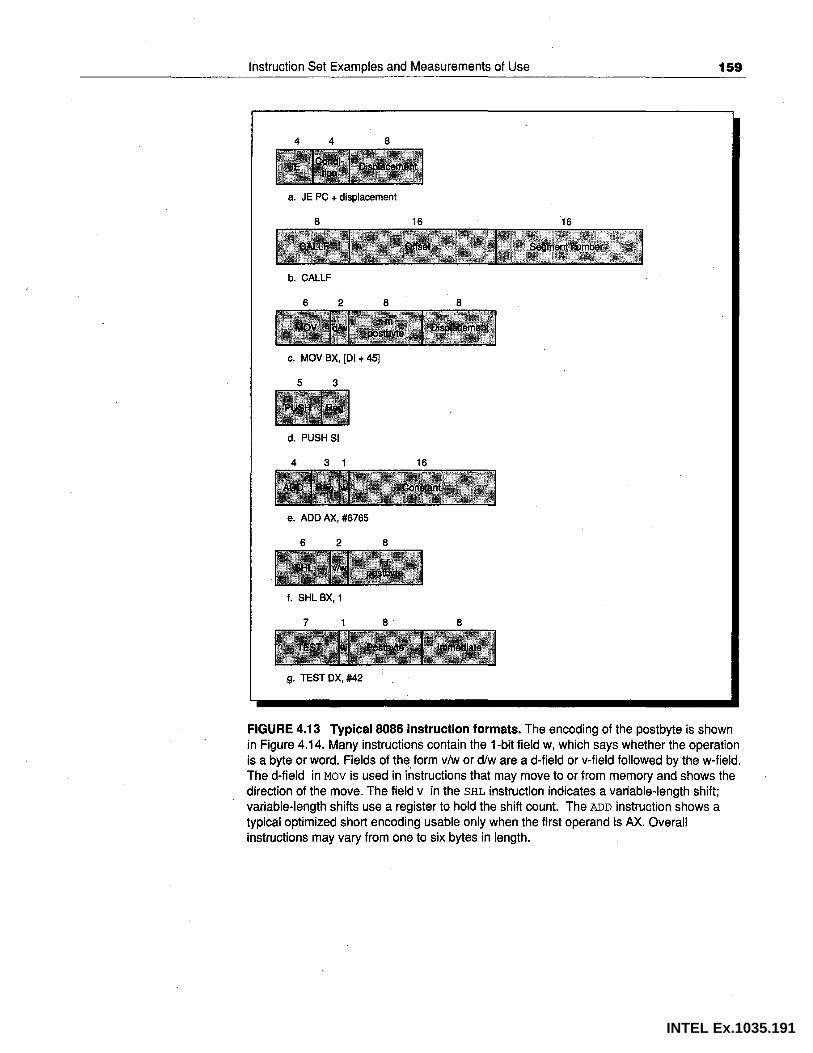
Instruction Set Examples and Measurements of Use 159
4. 4 8
a. JE PC + displacement
8 16 16
b. CALLF
6 2 8 8
c. MOV BX, [DI + 45]
5 3
d. PUSH SI
4 3 1 16
e. ADD AX, #6765
6 2 8
f. SHL BX, 1
7 a· 8
g. TEST DX, #42
FIGURE 4.13 Typical 8086 instruction formats. The encoding of the postbyte is shown in Figure 4.14. Many instructions contain the 1-bit field w, which says whether the operation is a byte or word. Fields of the form v/w or d/w are a d-field or v-field followed by the w-field. The d-field in Mov is used in instructions that may move to or from memory and shows the direction of the move. The field V in the SHL instruction indicates a variable-length shift; variable-length shifts use a register to hold the shift count. The ADD instruction shows a typical optimized short encoding usable only when the first operand is AX. Overall instructions may vary from one to six bytes in length.
INTEL Ex.1035.191

160 4.4 The 8086 Architecture
2 3 3
I 00 I ,, r1 ···•,·;I
Mem Indirect
2 3 3 8
I 01 I ,r1 .. •, l Mel)1 I I' Displac~lllen( ;I
8-bit •,
displacement -;c
2 3 3 16 '/'' ,''·'
10 r1 • ME\ITI . • . ·' .• ·. • IJisp1~6~fn~nt •• • .. ' •
I I 0. ~' ,·' I J I · i • •116-bit , displacement
~-·-·.'~·;:~··~~~~~~~~~~~.
2 3 3
r~tJ;,;~ .r1 •• J~.i( r~· .• 1 register-register
FIGURE 4.14 There are four postbyte encodings on the 8086 designated by a 2-bit tag. The first three indicate a register-memory instruction, where Mem is the base register. The fourth form is register-register.
4.5 I The DLX Architecture
In many places throughout this book we will have occasion to refer to a computer's "machine language." The machine we use is a mythical computer called "MIX." MIX is very much like nearly every computer in existence, except that is, perhaps, nicer ... MIX is the world's first polyunsaturated computer. Like most machines, it has an identifying number-the 1009. This number was found by taking 16 actual computers which are very similar to MIX and on which MIX can be easily simulated, then averaging their number with equal weight:
[(360 + 650 + 709 + 7070 + U3 + SS80 + 1107 + 1604 + G20 + B220 + S2000 + 920 + 601 + H800 + PDP-4+11)116)=1009.
The same number may be obtained in a simpler way by taking Roman numerals.
Donald Knuth, The Art of Computer Programming. Volume I: Fundamental Algorithms
INTEL Ex.1035.192

Instruction Set Examples and Measurements of Use 161
In this section we will describe a simple load/store architecture called DLX (pronounced "Deluxe"). The authors believe DLX to be the world's second polyunsaturated computer-the average of a number of recent experimental and commercial machines that are very similar in philosophy to DLX. Like Knuth, we derived the name of our machine from an average expressed in Roman numerals:
(AMD 29K, DECstation 3100, HP 850, IBM 801, Intel i860, MIPS M/120A, MIPS M/1000, Motorola 88K, RISC I, SGI 4D/60, SPARCstation-I, Sun-4/110, Sun-4/260) I 13 = 560 = DLX.
The architecture of DLX was chosen based on observations about the most frequently used primitives in programs. More sophisticated (and less performance-critical) functions are implemented in software with multiple instructions. In Section 4.9 we discuss how and why these architectures became popular.
Like most recent load/store machines, DLX emphasizes
• A simple load/store instruction set
• Design for pipelining efficiency (discussed in Chapter 6)
• An easily decoded instruction set
• Efficiency as a compiler target
DLX provides a good architectural model for study, not only because of the recent popularity of this type of machine, but also because it is an easy architecture to understand.
DLX-Our Generic Load/Store Architecture
In this section, the DLX instruction set is defined. We will use this architecture again in Chapters 5 through 7, and it forms the basis for a number of exercises and programming projects.
• The architecture has thirty-two 32-bit general-purpose registers (GPRs); the value of RO is always 0. Additionally, there are a set of floating-point registers (FPRs), which can be used as 32 single-precision (32-bit) registers, or as even-odd pairs holding double-precision values. Thus, the 64-bit floating-point registers are named FO, F2, ... , F28, F30. Both single- and double-precision operations .are provided. There are a set of special registers used for accessing status information. The FP status register is used for both compares and FP exceptions. All movement to/from the status register is
,_ through the GPRs; there is a branch that tests the comparison bit in the FP status register.
INTEL Ex.1035.193

162
Example instruction
LW Rl,30(R2)
LW Rl,lOOO(RO)
LB Rl,40(R3)
LBU Rl,40(R3)
LH Rl,40(R3)
LHU Rl,40(R3)
LF F0,50(R3)
LD F0,50(R2)
SW 500(R4),R3
SF 40(R3),F0
SD 40(R3),FO
SH 502 (R2), R3
SB 41 (R3) I R2
4.5 The DLX Architecture
• Memory is byte addressable in Big Endian mode with a 32-bit address. All memory references are through loads or stores between memory and either the GPRs or the FPRs. Accesses involving the GPRs can be to a byte, to a halfword, or to a word. The FPRs may be loaded and stored with singleprecision or double-precision words (using a pair of registers for DP). All memory accesses must be aligned. There are also instructions for moving between a PPR and a GPR.
• All instructions are 32 bits and must be aligned.
• There are also a few special registers that can be transferred to and from the integer registers. An example is the floating-point status register, used to hold information about the results of floating-point operations.
Operations
There are four classes of instructions: loads and stores, ALU operations, branches and jumps, and floating-point operations.
Instruction name Meaning
Load word Rlt-32 M [ 30+R2]
Load word Rlt-32 M[lOOO+O]
Load byte RH--32 (M[40+R3] o) 24 ## M[40+R3]
Load byte unsigned Rlt-32 024 ## M[40+R3]
Load halfword Rlt-32 (M[40+R3] o) 16 ##M[40+R3] ##M[41+R3]
Load halfword Rlt-32 Q16 ##M[40+R3] ##M[41+R3] unsigned
Load float FOt-32 M[50+R3]
Load double FO##Flf-64 M[50+R2]
Store word M [ 500+R4] f-32. R3
Store float M [ 40+R3] f-32 FO
Store double M [ 40+R3] f-32 FO; M[44+R3]f-32 Fl
Store half M [ 502+R2] f-16 R316 .. 31
Store byte M[4l+R3]f-g R224 .. 31
FIGURE 4.15 The load and store instructions in DLX. All use a single addressing mode and require that the memory value be aligned. Of course, both loads and stores are available for all the data types shown.
INTEL Ex.1035.194

Instruction Set Examples and Measurements of Use 163
Any of the general-purpose or floating-point registers may be loaded or stored; except that loading RO has no effect. There is a single addressing mode, base register + 16-bit signed offset. Halfword and byte loads place the loaded object in the lower portion of the register. The upper portion of the register is filled with either the sign extension of the loaded value or zeros, depending on the opcode. Single-precision floating-point numbers occupy a single floatingpoint register, while double-precision values occupy a pair. Conversions between single and double precision must be done explicitly. The floating-point format is IEEE 754 (see Appendix A). Figure 4.15 gives an example of the load and store instructions. A complete list of the instructions appears in Figure 4.18 (page 165).
All ALU instructions are register-register instructions. The operations include simple arithmetic and logical operations: add, subtract, AND, OR, XOR, and shifts. Immediate forms of all these instructions, with a 16-bit sign-extended immediate, are provided. The operation LHI (load high immediate) loads the top half of a register, while setting the lower half to 0. This allows a full 32-bit constant to be built in two instructions. (We sometimes use the mnemonic LI, standing for Load Immediate, as an abbreviation for an add immediate where one of the source operands is RO; likewise, the mnemonic MOV is sometimes used for an ADD where one of the sources is RO.)
There are also compare instructions, which compare two registers (=,:;t:,<,>,~.~). If the condition is true, these instructions place a 1 in the destination register (to represent true); otherwise they place the value 0. Because these operations "set" a register they are called set-equal, set-not-equal, set-lessthan, and so on. There are also immediate forms of these compares. Figure 4.16 gives some examples of the arithmetic/logical instructions.
Control is handled through a set of jumps and a set of branches. The four jump instructions are differentiated by the two ways to specify the destination address and by whether or not a link is made. Two jumps use a 26-bit signed offset added to the program counter (of the instruction sequentially following the jump) to determine the destination address; the other two jump instructions specify a register that contains the destination address. There are two flavors of jumps: plain jump, and jump and link (used for procedure calls). The latter places the return address in R31.
Example instruction Instruction name Meaning
ADD Rl,R2,R3 Add Rl~R2+R3
ADDI Rl,R2,#3 Add immediate Rl~R2+3
LHI Rl,#42 Load high immediate Rl~42##0 16
SLLI Rl,R2,#5 Shift left logical Rl~R2<<5
SLT . Rl, R2, R3 Set less than if (R2<R3) Rl~l ..
else Rl~O
FIGURE 4.16 Examples of arithmetic/logical instructions on DLX, both with and without immediates.
INTEL Ex.1035.195

164 4.5 The DLX Architecture
Example instruction Instruction name Meaning
J name Jump PC~name; ( (PC+4) -2 25 ) s name < ( (PC+4) +2 25
)
JAL name Jump and link R31~PC+4; PC~name;
( (PC+4) -2 25) s name < ( (PC+4) +2 25
)
JALR R2 Jump and link register R31~PC+4; PC~R2
JR R3 Jump register PC~R3
BEQZ R4,name Branch equal zero if (R4==0) PC~name;
( (PC+4)-2 15) :S name < ( (PC+4) +2 15
)
BNEZ R4,name Branch not equal zero if (R4 ! =0) PC~name;
( (PC+4) -2 15) :S name < ( (PC+4) +2 15
)
FIGURE 4.17 Typical control-flow instructions in DLX. All control instructions, except jumps to an address in a register, are PC-relative. If the register operand is RO, the branch is unconditional, but the compiler will usually prefer to use a jump with a longer offset over this "unconditional branch."
All branches are conditional. The branch_ condition is specified by the instruction, which may test the register source for zero or nonzero; this may be a data value or the result of a compare. The branch target address is specified with a 16-bit signed offset that is added to the program counter. Figure 4.17 gives some typical branch and jump instructions.
Floating-point instructions manipulate the floating-point registers and indicate whether the operation to be performed is single or double precision. Single-precision operations can be applied to any of the registers, while doubleprecision operations apply only to an even-odd pair (e.g., F4, F5), which is designated by the even register number. Load and store instructions for the floating-point registers move data between the floating-point registers and memory both in single and double precision. The operations MOVF and MOVD
copy a single-precision (MOVF) or double-precision (MOVD) floating-point register to another register of the same type. The operations MOVFP 2 I and MOVI 2FP move data between a single floating-point register and an integer register; moving a double-precision value to two integer registers require two instructions. Integer multiply and divide that work on 32-bit floating-point registers are also provided, as are conversions from integer to floating point and vice versa.
The floating-point operations are add, subtract, multiply, and divide; a suffix D is used for double precision and a suffix F is used for single precision (e.g., ADDD, ADDF, SUBD, SUBF, MU LTD, MULTF, D IVD, D IVF). Floating-point compares set a bit in the special floating-point status register that can be tested with a pair of branches: BFPT and BFPF, branch floating point true and branch floating point false.
Figure 4.18 contains a list of all operations and their meaning.
INTEL Ex.1035.196

Instruction Set Examples and Measurements of Use 165
Instruction type I opcode Instruction meaning
Data transfers Move data between registers and memory, or between the integer and FP or special registers; only memory address mode is 16-bit displacement + contents of
.. aGPR
LB,LBU,SB Load byte, load byte unsigned, store byte
LH,LHU,SH Load halfword, load halfword unsigned, store halfword
LW, SW Load word, store word (to/from integer registers)
LF,LD,SF,SD Load SP float, load DP float, store SP float, store DP float
MOVI2S, MOVS2I Move from/to GPR to/from a special register
MOVF, 1'10VD r Copy one floating-point register or a DP pair to another register or pair
MOVFP2I,MOVI2FP Move 32 bits from/to FP registers to/from integer registers
Arithmetic I Logical Operations on integer or logical data in GPRs; signed arithmetics trap on overflow
ADD,ADDI,ADDU,ADDUI Add, add immediate (all immediates are 16 bits); signed and unsigned
SUB,SUBI,SUBU,SUBUI Subtract, subtract immediate; signed and unsigned
MULT,MULTU,DIV,DIVU Multiply and divide, signed and unsigned; operands must be floating-point registers; all operations take and yield 32-bit values
AND,ANDI And, and immediate
OR,ORI,XOR,XORI Or, or immediate, exclusive or, exclusive or immediate
LHI Load high immediate-loads upper half of register with immediate
SLL, SRL, SRA, SLLI, SRLI, Shifts: both immediate (S_I) and variable form (S_) ; shifts are shift left logical, SRAI right logical, right arithmetic
s 's I Set conditional: "_"may be LT' GT' LE' GE' EQ' NE
Control Conditional branches and jumps; PC-relative or through register
BEQZ,BNEZ Branch GPR equal/not equal to zero; 16-bit offset from PC+4
BFPT,BFPF Test comparison bit in the FP status register and branch; 16-bit offset from PC+4
J, JR Jumps: 26-bit offs~t from PC (J) or target in register (JR)
JAL, JALR Jump and link: save PC+4 to R31, target is PC-relative (JAL) or a register (JALR)
TRAP Transfer to operating system at a vectored address; see Chapter 5
RFE Return to user code from an exception; restore user mode; see Chapter 5
Floating point Floating-point operations on DP and SP formats
ADDD,ADDF Add DP, SP numbers
SUBD,SUBF Subtract DP, SP numbers
MULTD,MULTF Multiply DP, SP floating point
DIVD,DIVF Divide DP, SP floating point
CVTF2D, CVTF2I, CVTD2F, Convert instructions: CVTx2y converts from type x to type y, where x and y are one CVTD2I, CVTI2F, CVTI2D of I (Integer), D (Double precision), or F (Single precision). Both operands are in the
FP registers
D, F DP and SP compares: "_" may be LT, GT, LE, GE, EQ, NE; sets comparison bit in FP -- --status register
FIGURE 4.18 Complete list of the instructions in DLX. The formats of these instructions are shown in Figure 4.19. This list can also be found in the back inside cover.
INTEL Ex.1035.197

166 4.5 The DLX Architecture
Instruction Format
All instructions are 32 bits with a 6-bit primary opcode. Figure 4.19 shows the instruction layout.
I - type instruction 6 5 5 16
Encodes: Loads and stores of bytes, words, half-words All immediates (rd .... rs1 op immediate)
Conditional branch instructions (rs1 is register, rd unused) Jump register, Jump and link register
· (rd = 0, rs = destination, immediate = 0)
R - type instruction 6 5 5 5 11
Register-register ALU operations: rd .... rs1 func rs2 Function encodes the data path operation: Add, Sub , ... Read/write special registers and moves
J - type instruction 6
Jump and jump and link Trap and RFE
26
FIGURE 4.19 Instruction layout for DLX. All instructions are encoded in one of three types.
Machines Related to DLX
Between 1985 and 1990 many load/store machines were announced that are similar to DLX. Figure 4.20 describes the major features of these machines. All have 32-bit instructions and are load/store architectures; the figure lists their differences. These machines are all very similar-if you 're not convinced, try making a table such as this one comparing these machines to the VAX or 8086.
DLX bears a close resemblance to all the other load/store machines shown in Figure 4.20. (See Appendix E for a detailed description of four load/store machines closely related to DLX.) Thus, the measurements in the next section will be reasonable approximations of the behavior of any of the machines. In fact, some studies suggest that compiler differences are more significant than architectural differences among these machines.
INTEL Ex.1035.198

Instruction Set Examples and Measurements of Use 167
Machine Registers Addressing modes Operations
DLX 32 integer; 16-bit displacement; See Figure 4.18. 16 DP or 32 SP FP 16-bit immediates
AMD29000 192 integer with stack Register deferred only; Integer multiply/divide trap to software. cache; 8-bitimmediates Branches =,=t- 0 only.
8DPFP
HP Precision 32GPRs 5-bit, 14-bit, and 32-bit Every ALU operation can skip the next in-
Architecture 32DP displacements; scaled struction. Many special bit-manipulation
or64 SPFP mode (load only); instructions. 32-bit immediates; decimal-autoincrement; support instructions: integer multiply/divide autodecrement not single instructions. Stores of partial word.
64-bit addresses possible through segmentation.
Intel i860 32 integer; 16-bit displacement; Branch compares two registers for equality.
16 DP or 32 SP FP indexed mode; Conditional traps are supported. FP autoincrement; reciprocal rather than divide. Some support 16-bit immediates for 128-bit loads and stores.
MIPS R2000/ 32 integer; 16-bit displacement; Floating-point load/store moves 32 bits to R3000 16FP 16-bit immediates upper or lower half of FP register. Branch
condition can compare two registers. Integer multiply/divide in GPRs. Special instructions for partial word load/store.
Motorola 32 GPRs 16-bit displacement; Special bit-manipulation instructions. 88000 indexed mode Branches can test for zero and also test bits
set by compares.
SPARC Register windows 13-bit offset and 13-bit Branches use condition code, set selectively with 32 integer immediates; indexed by instructions. Integer multiply/divide not registers available per addressing mode instructions. No moves between integer and procedure; FP registers. 16 DP or 32 SP FP
FIGURE 4.20 Comparison of the major features of a variety of recent load/store architectures. All the machines have a basic instruction size of 32 bits, though some provisions for shorter or longer are supported. For example, the
'Precision Architecture uses 2-word instructions for long immediates. Register windows and stack caches, which are used in the SPARC and AMD 29000 architectures, are discussed in Chapter 8. The MIPS R2000 is used in the DECstation 3100, the machine benchmarked in Chapter 2, and used as the load/store machine in Chapter 3. The number of doubleprecision floating-point registers is indicated if they are separate from the integer registers. Appendix E has a detailed comparative description of DLX, the MIPS R2000, SPARC, the i860, and the 88000 architectures. Both the MIPS and SPARC architectures have extensions that were not supported in hardware in the first implementation. These are discussed in Appendix E. In several of these machines RO=O, so they really have one less register available.
4.6 I Putting It All Together: Measurements of Instruction Set Usage
In this section we examine the dynamic use of the four instruction sets presented in this chapter. All instructions responsible for 1.5% or more of the instruction
INTEL Ex.1035.199

168 4.6 Putting It All Together: Measurements of Instruction Set Usage
executions in a set of benchmarks are included in measurements of each architecture. In the interest of conciseness, fractional percents are rounded so that all entries in the graphs of opcode frequency will be at least 2% ..
To facilitate comparisons among dynamic instruction set measurements, the measurements are organized by class of application. Figure 4.21 shows these application classes and the programs used to obtain instruction-use data on each of the machines discussed. We sometimes compare data for different architectures running the same type of application (e.g., a compiler) but different programs. The reader is cautioned that such comparisons must be made cautiously and with substantial limitations. Despite the fact that both programs may be the same type of application, differences in programming language, coding style, compilers, and so on, could substantially affect the results.
Machines Compilers Floating point General Business integer data
processing
VAX GCC Spice TeX COBOLX
360 PL/I FORTGO PLIGO COBOLGO
8086 Turbo C Assembler Lotus 1-2-3
DLX GCC Spice TeX US Steel
FIGURE 4.21 Programs used for reporting information about instruction mixes. There are four types of workloads, and each workload type has a representation programexcept that there is no floating-point program for the 8086. The inputs to GCC, Spice, and TeX used for the VAX were purposely shortened because the measurement process is very time intensive. (Readers who obtain measurements for the 360 or 8086 running GCC, Spice, or TeX and who are willing to share their data are asked to contact the publisher.)
In this section we present the instruction-mix measurements using a chart for each machine. The chart shows the average use of an instructiori across the programs measured for that architecture. The detailed individual measurements for each program can be found in Appendix C. This appendix will be needed as a reference to do the exercises and examples in the chapter.
Remember that these measurements depend on the benchmarks chosen and the compiler technology used. While the authors feel that the measurements in this section are reasonably indicative of the usage of these four architectures, other programs may behave differently from any of the benchmarks liere, and different compilers may yield different results. In doing a real instruction set study, the architect would want to have a much larger set of benchmarks, spanning as wide an application range as possible. He would also want to consider the operating system and its usage of the instruction set. Single-user benchmarks like those measured here do not necessarily behave in the same fashion as the operating system.
INTEL Ex.1035.200

Instruction Set Examples and Measurements of Use 169
VAX Instruction Set Measurements
The data on VAX instruction set usage in this section come primarily from measurements on our three benchmark programs. We add the data reported in another study for COBOL when we discuss opcode distributions. For these measurements, Spice and TeX were compiled with the globally optimizing versions of the VAX compilers originally developed for VMS (called VCC and fort). GCC cannot be compiled by the vcc compiler and hence uses the standard VAX 'cc compiler, which performs only peephole optimization. Once compiled, these programs were run with the Trace bit turned on. This causes the program to trap on every instruction execution, allowing a measurement program to collect data. Because this slows the program down by a factor of between 1,000 and 10,000 times, smaller inputs were used for the programs GCC, TeX, and Spice.
Addressing Mode Usage
Let's begin by looking at the VAX addressing modes, since the choice addressing modes and operations are orthogonal. First, we break the references into three broad classes: register, immediate (including short literal), and memory addressing modes. Figure 4.22 shows the breakdown into these three classes for our benchmarks. In all three programs, more than half the operand references are to registers.
About one-third of the operands on the VAX are memory references. How are those memory locations specified? The VAX memory addressing modes fall
TeX 25% Memory Spice 39%
GCC 30%
TeX 18% Immediate Spice 8%
GCC 19%
TeX 57% Register Spice 53%
GCC 51%
0% 10% 20% 30% 40% 50% 60%
FIGURE 4.22 Breakdown of basic operand types for the three benchmarks on the VAX. The frequencies are very similar across programs, except for the low usage of imrriediates by Spice and its correspondingly higher use of memory operands. This probably arises because few floating-point constants are stored as immediates, but are instead accessed from memory. An operand is counted by the number of times it appears in an instruction, rather than by the number of references. Thus, the instruction ADDL2
Rl, 45 (R2) counts as one memory reference and one register reference. The memory address modes in Figure 4.23 are counted in the same fashion. Wiecek [1982] reports that about 90% of the operand accesses are either a read or a write, and only about 10% of the accesses both read and write the same operand (such as Rl in the ADDL2).
INTEL Ex.1035.201

170
Example
4.6 Putting It All Together: Measurements of Instruction Set Usage
Auto increment TeX 1% Spice ~3% GCC 4%
Displacement TeX 2%
deferred Spice 7% GCC 2%
TeX 0% Scaled Spice
GCC ,..9%
Register TeX deferred Spice I 4%
GCC t
---=::-:----'I 20%
••••••• 41%
•••• 18%
TeX 56% Displacement Spice
GCC • ••••••••••••• 166% 67%
0% 10% 20% 30% 40% 50%' 60% 70% 80%
FIGURE 4.23 Use of VAX memory addressing modes, which account for about 31% of the operand references, in the three programs. Spice again stands out because of
the low frequency of register deferred. In Spice, nonzero displacement values occur much more frequently. The use of arrays rather than pointers probably influences this. Likewise, Spice uses the scaled mode to access array elements. The displacement deferred mode is used to access actual parameters in a FORTRAN subroutine. Remember that PC-based addressing is not included here-use of PC-based addressing can be measured by branch frequency.
into three separate classes: PC-based addressing, scaled addressing, and the other addressing modes (sometimes called the general addressing modes). The primary use of PC-based addressing is to specify branch targets, rather than data operands; thus, we do not include this addressing mode here. Scaled mode is counted as a separate addressing mode, and the. based mode on which it is built is counted as well. Figure 4.23 shows the use of addressing modes in the three benchmark programs. Not surprisingly, displacement mode dominates. Taken together, displacement and register deferred, which is essentially a special case of displacement with a zero constant value, constitute from 70% to 96% of the dynamically occurring addressing modes.
The size of a VAX instruction is almost always one byte for the opcode plus the number of bytes in the addressing modes. From these data the average size of an instruction can be estimated. Architects often do this type of estimating when they do not have exact measurements available. This is particularly true when data collection is expensive. Collecting the VAX data in this chapter, for example, took from one to several days of running time for each program.
The average VAX instruction has 1.8 operands. Use this fact and the data on displacement sizes in Figure 3.13 (on page 100 of Chapter 3) to estimate the average size of a VAX instruction. Such an estimate is useful for determining memory bandwidth per instruction, a critical design parameter.
INTEL Ex.1035.202

Answer
Instruction Set Examples and Measurements of Use 171
From the above data we know that literal and register modes, which each take 1 byte, dominate the mix. The most heavily used addressing mode, displacement mode, can vary from 2 bytes to 5 bytes-the register byte plus 1 or more offset bytes. Based on the length information in Figure 3.13 we guess that the average displacement is 1.5 bytes, for a total size of 2.5 bytes for the addressing mode. For this example, we assume that literal, register, and displacement modes make · up all the accesses. ' This means there is 1 byte for the opcode, 1 byte for register or literal mode, and about 2.5 bytes for displacement mode. Using 1.8 operands per instruction and the average frequencies of accesses from Figure 4.22 (page 169), we obtain 1 + 1.8 * (0.54 + 0.15 + 0.31 * 2.5) or 3.64 bytes7
Wiecek [1982] measured 3.8 bytes per instruction. Direct measurements of our three programs showed the average sizes to be 3.6, 4.9, and 4.2 for GCC, Spice, and TeX, respectively.
Instruction Mixes
Now let's look at the distribution for instruction operations, using our three benchmarks plus the COBOLX program from the study published by Clark and Levy [1982]. COBOLX is a synthetic, internal DEC benchmark that was compiled by the VAX VMS COBOL compiler and uses decimal instructions. However, the new DEC compilers for the VAX avoid using the decimal instruction set, since most of that portion of the architecture is emulated in software-and is therefore much slower--on the newer VLSI-based VAXes.
The data in this section are presented in chart form, but detailed tables for each machine and benchmark appear in Appendix C. The data here focus on instruction frequency, but frequency distributions and time distributions do not always match. We will see an example of this in the next section. Appendix D contains a set of detailed measurements based on time-distribution measurements.
Figure 4.24 shows all instructions responsible for more than .1.5% of the dynamic instruction executions across all the benchmarks. Each complete bar. shows an average instruction mix over the four programs, and how the programs make up that mix.
GCC and TeX are very similar in behavior; the largest difference is the higher frequency of data transfers in TeX. Spice and COBOLX look very different. Each of these executes more than 20% of its instructions using a portion of the instruction set that is essentially unused by the other benchmarks. Both COBOLX and Spice do many fewer integer arithmetic operations, instead using decimal or floating-point operations. COBOLX makes small use of the data transfer instructions ( 4% versus an average of 20%. for the other three programs); instead, 38% of the instructions it executes are decimal or string instructions.
These 27 instructions in Figure 4.24 correspond to an average of 88% of the instructions executed in the four benchmarks. However, the tail of the
INTEL Ex.1035.203

172 4.6 Putting It All Together: Measurements of Instruction Set Usage
Decimal, string
Floating point
Data transfer
Arithmetic, logical
Control Procedure
CMPC3 CMPP_ ADDP4 MOVC3, MOVC5 CVTTP,CVTPT
CMPD DIVD ADDO_ SUBD_ MULD_
MOVZ*L MOVQ PUSHL MOVL
MULL_ ASHL CVT*L sus·_ CLRL TSTL MOVA* INCL ADDL_ CMP*
JMP RET CALLS, CALLG BRB, BRW Conditional Branch - - 5%
---- 17%
~ 8 ~RR 1~ 18 1~18 18
• GCC 0 Spice • TeX Ill COBOLX ~
FIGURE 4 .. 24 The VAX instruction frequencies combined graphically. The total size of each bar shows the behavior that would be seen on a machine that ran these four programs with equal frequency. The segments of the bar show what percentage of the usage of that instruction would come from each of the programs. This illustrates that some portions of the instruction set need to be there for only one class of applications. Overall, only a small number of instructions outside of the control, data transfer, and integer arithmetic instructions are heavily used.
distribution is long and there are many instructions executed with a frequency of 1/2 to 1 %. In Spice, for example, the top 15 instructions make up 90% of the executions, and the top 26 make up 95%. However, there are 149 different VAX instructions executed at least once!
Measurements of 360 Instruction Set Usage
The measurements in this section are taken from those made by Shustek in his Ph.D. thesis [1978]. His work includes a study of the dynamic characteristics of
INTEL Ex.1035.204

Instruction Set Examples and Measurements of Use 173
seven large programs on the IBM 360 architecture. He collected his data by building an interpreter for the 360 architecture. The four programs described in Figure 4.25 are used in this section to examine characteristics of 360 instruction set usage.
Program Benchmark class Instruction count Program function
COBOLGO Business D.P. 3,559,533 COBOL usage report formatter
PLIGO General integer 23,863,497 PL/I computer usage accounting
FORTGO Floating point 11,719,853 FORTRAN linear systems solver
PLIC Compiler 24,338,101 PL/I compile
FIGURE 4.25 Four programs used to measure the IBM 360. The suffix "GO" indicates an execution of a program, while the suffix "C" indicates a compile. We chose the PUI compiler because it is the largest and most representative; it is also written in PUI. Shustek's thesis used two FORTRAN executions. We chose to use LINSYS2 to represent the FORTRAN execution, since it is a more typical FORTRAN program; we refer to the execution of LINSYS2 as FORTGO.
Addressing Modes and Instruction Types
Figure 4.26 shows the frequency of data accesses by addressing mode. The COBOL program has a very high frequency of data accesses. Movements of character data and use of decimal data, which always reside in memory, probably account for this. FORTGO has a substantially lower number of memory references. This may arise because of allocation of variables to registers in the tight inner loops of the program.
COBOL GO 79%
Memory PUGO FORTGO PUC
COBOLGO Immediate PUGO
FORTGO PUC
COBOLGO Register PUGO
FORTGO 81% PUC 62%
0% 10% 20% 30% 40% 50% 60% 70% 80% 90%
FIGURE 4.26 Distribution of operand accesses made by 360 instructions. Limited support for immediates is the chief reason that immediates see so little use.
INTEL Ex.1035.205

174
Example
Answer
4.6 Putting It All Together: Measurements of Instruction Set Usage
There an~ only two memory addressing modes on the 360: base register + displacement (RS format, SI format, and SS format) and base register + displacement + index register (RX format). However, the operations available in the instructions that address memory typically appear in only one format. Therefore, it is probably most useful to look at instruction format usage, as shown in Figure 4.27. Most instructions are RX format with RR following behind that. The high usage of RX format should not lead .you to conclude that the displacement + base register + index register addressing mode is heavily used, because in 85% of the RX instructions the index register is zero. COBOL displays a high percentage of SS-format instructions, and this is to be expected because the decimal and string instructions are all SS format. The FORTRAN execution displays a large percentage of RR format, 2-byte instructions. This makes sense in a program that makes heavy use of registers in its optimized inner loops.
FIGURE 4.27 Percentage of 6-, 4-, and 2-byte instructions for the four 360 programs. The majority of the instructions are 4 bytes, and almost none are 6 bytes, except when running COBOLGO.
Given th,e data in Figure 4.27 compute the average instruction length for the PLIGO program.
The average instruction length is
6 * % SS + 4 * (% RX + % RS + % SI) + 2 * % RR
= 0 + 4 * (0.63+ 0.04+0.17) + 2 * 0.16 = 3.68 bytes
Across all the four programs the average measured length is 3.7 bytes.
INTEL Ex.1035.206

Instruction Set Examples and Measurements of Use
ED 0% CP
CLC Decimal, MP
strin~ CVD ZAP
AP MVC 3%
Floating MDR point AD
LTR IC
LH Data LPDR
transfer STD LD ST 3%
MVI 5% L,LR 19%
MH TM c 3%
Arithmetic, NI logical CLI
LA SLL SR
A,AR 10%
Control, BAL, BALR procedure BC, BCR 15%
~ 8 ~RR 1~ 181~18 18~
• PUC D FORTGO D PLIGO • COBOLGO I
FIGURE 4.28 Combined data for the four programs on the 360. Compare this with Figure 4.24, where the data for the VAX are graphed.
Instruction Mixes
175
Now let's examine the data for the instruction mixes. Figure 4.28 shows the most heavily used instructions in the four 360 benchmarks. As Figure 4.28 illustrates, variations among the programs are very large. The PL/I compiler has an extraordinarily large number of branches, while the PL/I execution has very few. The use of arithmetic and logical operators is fairly uniform with the exception of the COBOL program, which uses decimal operations instead.
Cqmparing these programs to the VAX, the much lower frequency of branches~J6% on the 360 versus 23% on the VAX-stands out. The number of branches in a program is largely fixed by the program, except for some architectural anomalies and possible compiler optimizations (such as loop unrolling-discussed in Chapter 6-but not used by these compilers). Thus, the
INTEL Ex.1035.207

176 4.6 Putting It All Together: Measurements of Instruction Set Usage
percentage of branches is an indirect measure of instruction power or density, since it says how many other instructions are required for each branch. We would expect the VAX with its more powerful addressing modes and multiple memory operands per instruction to have a high instruction density and a higher branch frequency. We see further evidence of greater instruction density of the VAX in the higher frequency of data transfers on the 360-more data is moved explicitly on the 360 rather than used as memory operands, as on the VAX. However, we cannot draw any specific quantitative conclusions about instruction density because the measured programs and compilers are different.
Also very different is the percentage of character and string operations used by the 360 versus the VAX for the two COBOL applications. Finally, the FORTRAN execution uses a much larger number of integer operations on the 360; this may be traceable to differences arising when the VAX uses an addressing mode but the 360 must use explicit instructions for address calculations.
As we have seen, the differences in instruction usage on the 360 and VAX are fairly significant. The next two architectures differ from these first two even more dramatically.
Measurements of 8086 Usage
The data in this section were collected by Adams and Zimmerman [1989] in a study of seven programs running on an IBM PC under MS DOS 3.1. They collected the data by single.-stepping the programs and collecting data after every instruction execution, just as was done for the VAX. The three programs
. used here, a brief description, and the number of instructions executed are shown in Figure 4.29. As with the VAX and 360, we will begin by examining operand access and addressing modes, and then progress to instruction mixes.
Addressing Modes and Instruction Length
Our first measurement on the 8086, shown in Figure 4.30, graphs the origins of operands. Immediates play a small role, while register access slightly dominates memory access. Compared to the VAX, these programs on the 8086 use a higher frequency of memory operands. The limited register set of the 8086 probably
Program Benchmark class Instruction count Program function
Lotus Business 2,904,931 Lotus 1-2-3 calculating a 128-cell worksheet four times
MASM General integer 2,365,711 Microsoft Macro Assembler assembling a 500-line program
Turbo C Compiler 1,806,143 Turbo C compiling Dhrystone
FIGURE 4.29 Three programs used for 8086 measurements. The benchmarks are written in a combination of 8086 Assembler and in C.
INTEL Ex.1035.208

Instruction Set Examples and Measurements of Use 177
plays a role in increasing the memory traffic, which substantially exceeds that of the 360, if we ignore the COBOL program (which must use SS instructions) on the 360.
Lotus 43% Memory Assembler 37%
Turbo C 43%
Lotus Immediate Assembler 7%
Turbo C 11 %
Lotus 52% Register Assembler 55%
Turbo C 46%
0% 5% 10% 15% 20% 25% 30% 35% 40% 45% 50% 55%
FIGURE 4.30 Three classes of basic operand access on the 8086 and their distribution. The implied use of the accumulator register (AX), which occurs in a number of instructions, is counted as a register access.
In the above programs 41 % of the operand references are memory accesses. Figure 4.31 shows the distribution of addressing modes for these memory references.
Lotus 15% Indirect Assembler
Turbo C
Lotus 34% Absolute Assembler 36%
Turbo C 18%
Lotus 51% Displacement Assembler 52%
Turbo C 73%
0% 10% 20% 30% 40% 50% 60% 70% 80%
FIGURE 4.31 The 8086 memory addressing modes shown in this graph account for. almost all the memory references in the three programs. Memory addressing modes indexed and based have been combined, since their effective address calculations are the same. Register indirect mode is in effect based with a zero offset, equivalent to the VAX register-deferred mode. If register indirect were counted as a based mode with zero offset, about two-thirds of the memory references would be displacement mode. The other two remaining modes are essentially unused in the three programs.
The variable-length instructions, use of implicit registers, and small size of the register specifier combine to yield a fairly short average instruction. For these three programs the average instruction length is approximately 2.5 bytes.
INTEL Ex.1035.209

178 4.6 Putting It All Together: Measurements of Instruction Set Usage
Instruction Mixes on the 8086
The instructions responsible for greater than 1.5% of the executions for the 8086 running the three programs are shown graphically in Figure 4.32. The displayed subset of the instruction set accounts for a higher proportion of all instruction executions (90%) than it does on the VAX or 360. As we might suspect, the architectures with smaller instruction repertoires use a higher percentage of their opcodes.
The major distinguishing characteristic among the programs is the shift from data transfer instructions to control instructions in Lotus. Lotus makes heavy use of the LOOP instruction, which may account for that shift.
The overall frequency of move instructions is much larger on the 8086 than on the VAX. This difference probably arises because the 8086 has fewer general-purpose registers. Other possible explanations include the use of string instructions that generate a sequence of move in.structions, and explicit movement of data among segments to ease processing. The total branch frequency is not very different between the 8086 and VAX, though the distribution of different types of control instructions is very different. The percentage of arithmetic operations on the 8086 is much smaller, due at least partially to the larger number of move instructions.
POP_.____,
Datas PUSH ••CJll transfer LES
MOV ............ c:::::=:::::=:::::=:::::=:::::=:::Jliiil!lil!lli'll!IJ27%
TEST
CBW
SUB
Arithmetic, INC, DEC logical OR, XOR
ADD
SAL, SHR, RCR
CMP
JMP
Control, LOOP
procedure RET,RETF call CALL, CALLF
Conditional Jump 10%
0% 5% 10% 15% 20% 25% 30%
• Turbo C 0 MASM Ill Lotus i
FIGURE 4.32 Distribution of instruction frequencies on the 8086 shown in the same format used for the VAX and 360. ·
INTEL Ex.1035.210

Example
Answer
Instruction Set Examples and Measurements of Use 179
In this and the preceding two sections we saw machines designed in the 1960s (the 360) and the 1970s (the VAX and the 8086). In the next section we will talk about a machine typical of those designed in the 1980s and its usage.
Instruction Set Usage Measurements on DLX
As with the other architectures we have looked at thus far, we start our examination of instruction set usage on DLX with measurements of operand location and move from there to instruction mixes. The DLX data throughout the book was measured using the MIPS R2000/3000 architecture and adjusting the data to reflect the differences between DLX and the MIPS architecture. The MIPS compiler technology with optimization level 2, which does full global optimization with register allocation, was used to compile the programs. A special program called pixie was used to instrument the object module. The instrumented object module produces a monitoring file that is used to produce detailed execution statistics.
Addressing Mode Usage
Operand usage is shown in Figure 4.33. This data is very uniform across the applications on DLX. Compared to the VAX, a much higher percentage of the operand references are to registers: On the VAX, only about half the references are to registers, while roughly three-quarters are on DLX. This probably occurs because of the larger number of registers available on DLX and greater emphasis on register allocation by the DLX compiler.
Since D1=-X has only a single addressing mode, it makes no sense to ask what the distribution of addressing modes is. However, we noticed earlier that on the VAX and 8086 the deferred addressing mode, which is equivalent to displacement addressing with a zero displacement, was the second or third most popular. Would it be useful to add this mode to DLX?
Using the data on offset values from Figure 3.13 .on page 100, determine how often on average deferred mode would be used for the three programs if the case of a zero-offset displacement were made a special mode. In particular, what percentage of the memory references would use it? How much memory bandwidth would be saved if we had a 16-bit instruction for this addressing mode?
The frequencies of zero-off set displacement values are
GCC: 27%
Spice: 4%
TeX: 17%
INTEL Ex.1035.211

180 4.6 Putting It All Together: Measurements of Instruction Set Usage
The average frequency for a zero-offset value is then (27% + 4% + 17% )/3 = 16%. Thus, the mode would be used by 16% of the loads and stores, which average 17..% of the executions. The decrease in instruction bandwidth would be
1 about 2 * 32% * 16%, or about 3%.
TeX 18% Memory Spice 16%
GCC 16%
TeX Immediate Spice
GCC
TeX 73% Register Spice 78%
GCC 75%
0% 10% 20% 30% 40% 50% 60% 70% 80%
FIGURE 4.33 Distribution of operand accesses for the three benchmarks on DLX. Only accesses for operands-not for effective address calculations-are included. The fact that DLX has only 3-operand register formats probably increases the frequency of register operand access slightly, since some instructions probably have only two unique register operands and use one register as both a source and destination. On a machine like the VAX, such an operation might use a 2-operand instruction and thus be counted as having only 2 register operands. This effect has not been measured.
The other two addressing modes used with some frequency are scaled on the VAX and absolute on the 8086. Scaled addressing mode is synthesized on DLX with a separate add; the presence of this address mode is significantly affected by the compiler technology. Better optimizers use the indexed mode less often because the optimization of induction variable elimination obviates the need for indexed addressing and for scaling (see the discussion in Section 3.7). The direct mode is synthesized by dedicating a register to point to a global area and accessing variables with a displacement from that register. Because only scalar variables (i.e., not structures or arrays) need to be accessed in this way, this works very well for most programs.
Instruction Mixes on DLX
Figure 4.34 shows the instruction mixes for our three programs plus the U.S. Steel COBOL benchmark-the most widely employed COBOL benchmark. The benchmark is a synthetic program of about 1,000 lines in length. It is included here because its behavior is substantially different from FORTRAN and C programs. Measurements on COBOL are also interesting because they reflect what changes in instruction set usage occur when decimal arithmetic is not
INTEL Ex.1035.212

Instruction Set Examples and Measurements of Use 181
directly supported by decimal instructions. Let's first look at the differences among the programs before we consider how these mixes compare to the VAX.
The significant differences among these programs are surprising. Both Spice and TeX stand out as having very low branch frequency. The effect of translating the decimal arithmetic of COBOL into binary arithmetic is clearly seen in the large percentage of arithmetic operations in US Steel. Shifts, logical operators, and load immediates, which are all used to do fast decimal-binary conversion, occur in significant frequencies. US Steel's low frequency of data transfer is certainly affected by this increase in arithmetic and logical operations. Interestingly, only the call frequency of US Steel is high enough to account for more than 1 % of the instruction executions (the frequency of JAL is about 1 % for the other three benchmarks).
Floating point
Data transfer
Arithmetic, logic
DIVD
SUBD
ADDO
MULD
MOV*
SD
LD
LBU
SW
LW
OR,ORI
SRA
AND.ANDI
S--,S--1 ·-·
4%
LI •••• 4%
SLL 4%
LHI ~:::J-•ill 5%
7%
13%
ADDU, ADDUI ····====-••••&llllillillillilli/I 20%
Control, procedure call
JR
JAL
J
B--Z !!!!!!!!!~~~~~~~~1:,.:1o/c~o _, ____ _
0% 5% 10% 15% - 20%
Total Dynamic Count
• GCC D Spice • TeX Ill US Steel •
FIGURE 4.34 The DLX instruction mix visible over four programs with breakdown showing each program's contribution. What is remarkable is how a small number of instructions-conditional branch, add, load, and store-dominate across all four programs. The opcode LI is really an ADDUI with RO as an operand; the high frequency of ADDU and ADDUI is discussed below.
INTEL Ex.1035.213

182
Example
Answer
4.6 Putting It All Together: Measurements of Instruction Set Usage
These mixes differ dramatically from the VAX (or other machines in this section). One difference is the very high percentage of ADDU and ADDUI
instructions. These instructions are used for a variety of purposes where the other machines may use a different instruction or a more powerful addressing mode or instruction. Among the most frequent uses for ADDU and ADDUI are: register-register copies (coded as ADDU with RO), synthesizing an address mode such as scaled, and incrementing the stack pointer on a procedure call.
It is interesting to compare the branch frequency between DLX and the VAX, since the absolute branch count should be approximately equal (for reasons discussed earlier), and the ratio of branch frequencies should be about the same as the ratio of overall instruction counts. However, the compilers may affect the type of branch used-conditional branch versus jump-so we need to combine all the branches and jumps, except those used in procedure calls, to make a comparison.
Find the ratio of absolute branches on the VAX versus DLX for the three common benchmarks. The ratio of instruction counts, measured in Section 3.8 is
InstructionsDLX = 2.0 Instructions VAX
Use the data in Appendix C for exact percentages of branches.
From Appendix C, we find that the average branch frequency on DLX is 19%+2%+7% . . .
3 = 9.3%, while the average for the VAX is 17.3%. Thus, the ratio
of the branch counts is
BranchesnLX 9.3% * lnstructionsnLx =
BranchesvAX 17.3% * InstructionsvAX
9.3 * 2.0 * Instructionsv AX = 17 .3 * Instructionsv AX
= 18.6 = 1 08 17.3 .
So DLX does about 8% more branches.
In the arithmetic and logical instructions, GCC and US Steel are the most different between the VAX and DLX. We know US Steel differs because of the absence of decimal instructions-it would be interesting to see what the instruction mix on such a program would look like with the new VAX compilers that avoid the decimal instructions. Another major difference between the two machines is the lower frequency of compare instructions and test instructions on DLX. The use of compare with zero in the branch instruction is responsible for
INTEL Ex.1035.214

Instruction Set Examples and Measurements of Use 183
this. Because the set instructions are also used to set logical variables, we cannot know exactly what percentage of conditional branches on DLX do not need a compare, but we can guess that it is between 75% and 80%.
The difference in data transfers has been discussed extensively at the end of Chapter 3 (for a machine very close to DLX) and in the previous subsection. We know that the larger number of registers (at least twice as many) and more ambitious register allocator mean that the load and store frequency is lower on DLX than on the VAX.
We have now seen instruction mixes for four very different machines. In Appendix D we can see how these mixes differ when we look at time distributions rather than frequency of occurrence, and in the next section we will review some of our key observations and point out some additional pitfalls using data we have examined in this and earlier sections.
4. 7 I Fallacies and Pitfalls
Fallacy: There is such a thing as a typical program.
Many people would like to believe that there is a single "typical" program that could be used to design an optimal instruction set. For example, see the synthetic benchmarks discussed in Section 2.2. The data in this chapter clearly show that programs can vary significantly in how they use an instruction set. For example, the frequency of control-flow instructions on DLX varied from 5% to 23%. The variations are even larger on an instruction set that has specific features for supporting a class of applications, such as decimal or floating-point instructions that are unused by other applications. There is a related pitfall.
Pitfall: Designing an architecture on the basis of small benchmarks or large benchmarks from a restricted application domain when the machine is intended to be general purpose.
Many programs exhibit somewhat biased behavior or do not use a particular aspect of an architecture. Obviously, choosing TeX or GCC benchmarks to design the instruction set might result in a machine that wouldn't do well on a program like Spice or COBOLX. A more subtle example arises when choosing a representative, but synthetic, benchmark. For example, Dhrystone (see Section 2.2) does a procedure call approximately every 40 instructions on a machine like DLX-the number of procedure calls is more than half the number of conditional branches!. By comparison, in GCC a call occurs about once every 100 instructions, and branches are 15 times more frequent than procedure calls.
Faltacy: An architecture with flaws cannot be successful.
The IBM 360 is often criticized in the literature-the branches are not PCrelative, and the offset is too small in based addressing. Yet, the machine has
INTEL Ex.1035.215

184 4.7 Fallacies and Pitfalls
been an enormous success because it did several new things properly. First, the architecture has a big enough address space. Second, it is byte addressed and handles bytes well. Third, it is a general-purpose register machine. Finally, it is simple enough that it can be efficiently implemented across a wide performance and cost range.
The 8086 provides an even more dramatic example. The 8086 architecture is the only widespread architecture in existence today that is not truly a generalpurpose register machine. Furthermore, the segmented address space of the 8086 causes major problems both for programmers and compiler writers. Despite these major difficulties, the 8086 architecture-because of its selection as the microprocessor in the IBM PC-has been enormously successful.
Fallacy: One can design a flawless architecture.
All architecture design involves tradeoffs made in the context of a set of hardware and software technologies. Over time those technologies are likely to change, and decisions that may have been correct at the time they were made look like mistakes. For example, in 1975 the VAX designers overemphasized the importance of code-size efficiency and underestimated how important ease of decoding and pipelining would be ten years later. Almost all architectures eventually succumb to the lack of sufficient address space. However, avoiding this problem in the·long run would probably mean compromising the efficiency of the architecture in the short run.
Fallacy: In instruction mixes, time distribution and frequency distribution will be close.
Appendix D shows the time distributio11s for our benchmark programs and compares the time and frequency distributions. A simple example of where these distributions are very different is in the COBOLGO program on the 360. Figure 4.35 shows the top instructions by frequency and by time. The two highest occurring instructions are responsible for 33% of the instruction executions in · COBOLGO, but only 4% of the execution time! Remember that time distributions are dependent on both the architecture and the implementation used for the measurement. Hence, time distributions may differ from model to model, while frequency distributions will be the same, provided neither the software nor the program changes. This large difference between time and frequency distributions does not exist for simpler load/store architectures, such asDLX.
Pitfall: Examining only the worst-case or average behavior of an instruction as design input.
The best example of this comes from the use of MVC on an IBM 360. The instruction can move overlapped fields of characters, but this occurs less than 1 % of the time, and then usually to clear a field. The average length of a move
INTEL Ex.1035.216

Instruction Set Examples and Measurements of Use 185
as measured by Shustek was ten bytes, but more than three-quarters of the moves were either one byte or four bytes in length. Assuming worst-case behavior (overlapping strings) or average length can each lead to suboptimal design decisions.
Top instructions by Frequency Top instructions by Percentage frequency time distribution of time
L, LR 19% ZAP 16%
BC, BCR 14% AP 16%
AP 11% MP 13%
ZAP 9% MVC 9%
MVC 7% CVD 5%
FIGURE 4.35 The top five instructions by frequency and by time for the COBOLGO benchmark run on the 360. The actual frequency or percentage of time is also shown. Further data appears in Appendix D.
4.8 I Concluding Remarks
We have seen that instruction sets can vary quite dramatically, both in how they access operands and in the operations that can be performed by a single instruction. The comparison of opcode usage across architectures by instruction frequency is summarized in Figure 4.36. This figure shows that even very different architectures behave similarly in their use of instruction classes. However, this should also remind us that performance may be only distantly related to instruction usage-the execution-time distributions for these architectures in Appendix D look very different indeed.
Dramatic though the variation in instruction usage is across architectures, it is equally dramatic across applications. We have seen that floating-point programs, COBOL programs, and C systems programs differ in how they use a machine. Large segments of the instruction set are unused by some programs. When such application-specific features are not part of the instruction set-for example, the absence of decimal instructions in DLX-the impact is a shift in the use of other parts of the instruction. Even across two programs written in the same language-GCC and TeX, or PLIC and PLIGO-the differences in instruction usage can be significant.
Instruction-usage data are an important input for the architect, but they do not .necessarily tell us what are the most time-consuming instructions. The next several chapters will help explain why the difference arises by quantifying the CPI difference among instructions and machines.
INTEL Ex.1035.217

186 4.9 Historical Perspective and References
Machine Program Control Arithmetic, Data Floating Decimal, Totals logical transfer point string
VAX GCC 30% 40% 19% 89%
VAX Spice 18% 23% 15% 23% 79%
VAX TeX 30% 33% 28% 91%
VAX COBOLX 25% 24% 4% 38% 91%
360 PLIC 32% 29% 17% 4% 82%
360 FORTGO 13% 35% 40% 7% 95%
360 PLIGO 5% 29% 56% 90%
360 COBOLGO 16% 9% 20% 40% 85%
8086 Turbo C 21% 23% 49% 93%
8086 MASM 20% 24% 46% 90%
8086 Lotus 32% 26% 30% 88%
DLX GCC 24% 35% 27% 86%
DLX Spice 4% 29% 35% 15%( 83%
DLX TeX 10% 41% 33% 84%
DLX US Steel 23% 49% 10% 82%
FIGURE 4.36 The frequency of instruction distribution for each benchmark broken into five classes of instructions. Because only instructions with frequencies greater than 1.5% have been included in previous figures, the totals are less than 100%.
Historical Perspective and References
Although a large number of machines have been developed in the same time frames as the four machines covered in this chapter, the discussion here is confined to these machines and measurements of them.
The IBM 360 was introduced in 1964 with six models and a 25:1 performance ratio. Amdahl, Blaauw, and Brooks [1964] discuss the architecture of the IBM 360 and the concept of permitting multiple object-code-compatible implementations. The notion of an instruction set architecture as we understand it today was the most important aspect of the 360. The architecture also introduced several important innovations, now in wide use:
1. 32-bit architecture
2. Byte-addressable memory with 8-bit bytes
3. 8-, 16-, 32-, and 64-bit data sizes
In 1971, IBM shipped the first System/370 (models 155 and 165), which included a number of significant extensions of the 360, as discussed by Case and Padegs [1978], who also discuss the early history of System/360. The most important addition was virtual memory, though virtual memory 370s did not ship until 1972 when a virtual-memory operating system was ready. By 1978,
INTEL Ex.1035.218

Instruction Set Examples and Measurements of Use 187
the high-end 370 was several hundred times faster than the low-end 360s shipped ten years earlier. In 1984, the 24-bit addressing model built into the IBM 360 needed to be abandoned, and the 370-XA (eXtended Architecture) was introduced. While old 24-bit programs could be supported without change, several instructions could not function in the same manner when extended to a 32-bit addressing model (31-bit addresses supported) because they would not produce 31-bit addresses. Converting the operating system, which was written mostly in assembly language, was no doubt the biggest task.
Several studies of the IBM 360 and instruction measurement have been made. Shustek's thesis [1978] is the best known and most complete study of the 360/370 architecture. He made several observations about instruction set complexity that were not fully appreciated until some years later. Another important study of the 360 is the Toronto study by Alexander and Wortman [1975] done on an IBM 360 using 19 XPL programs.
In the mid-1970s, DEC realized that the PDP-11 was running out of address space. The 16-bit space had been extended in several creative ways. However, as Strecker and Bell [1976] observed, the small address space was a problem that could not be overcome, but only postponed.
In 1978, DEC introduced the VAX. Strecker [1978] described the architecture and called the VAX "a Virtual Address eXtension of the PDP-11." One of DEC's primary goals was to keep the installed base of PDP-11 customers. Thus, the customers were to think of the VAX as a 32-bit successor to the PDP-11. A 32-bit PDP-11 was possible-there were three designs-but Strecker reports that they were "overly compromised in terms of efficiency, functionality, programming ease." The chosen solution was to design a new architecture and include a PDP-11 compatibility mode that would run PDP-11 programs without change. This mode also allowed PDP-11 compilers to run and to continue to be used. The VAX-11/780 was made similar to the PDP-11 in many ways. These are among the most important:
1. Data types and formats are mostly equivalent to those on the PDP-11. The F and D floating formats came from the PDP-11. G and H formats were added later. The use of the term "word" to describe a 16-bit quantity was
'J carried from the PDP-11 to the VAX.
2. The assembly language was made similar to the PDP-11 's.
3. The same buses were supported (Unibus and Massbus).
4. The operating system, VMS, was "an evolution" of the RSX-1 lM/IAS OS (as opposed to the DECsystem 10/20 OS, which was a more advanced system).
5. The file system was basically the same. ·~
The VAX-11/780 was the first machine announced in the VAX series. It is one of the most successful and heavily studied machines ever built. The cornerstone of DEC's strategy was a single architecture, VAX, running a single
INTEL Ex.1035.219

188 4.9 Historical Perspective and References
operating system, VMS. This strategy worked well for over ten years. The large number of papers reporting instruction mixes, implementation measurements, and analysis of the VAX make it an ideal case study.
Wiecek [1982] reported on the use of various architectural features in running a workload consisting of six compilers. Erner did a set of measurements (reported by Clark and Levy [1982]) on the instruction set utilization of the v_ AX when running four very different programs and when running the operating system. A good detailed description of the architecture, including memory management and an examination of several of the VAX implementations, can be found in Levy and Eckhouse [1989].
The first microprocessors were produced late in the first half of the 1970s. The Intel 4004 and 8008 were extremely simple 4-bit and 8-bit accumulatorstyle machines. Morse et al. [1980] describe the evolution of the 8086 from the 8080 in the late 1970s in an attempt to provide a 16-bit machine with better throughput. At that time almost all programming for microprocessors was done in assembly language-both memory and compilers were in1short supply. Intel wanted to keep its base of 8080 users, so the 8086 was designed to be "compatible" with the 8080. The 8086 was never object-code compatible with the 8080, but the machines were close enough that translation of assembly language programs could be done automatically.
In early 1980, IBM selected a version of the 8086 with an 8-bit external bus, called the 8088, for use in the IBM PC. (They chose the 8-bit version to reduce the cost of the machine.) This choice, together with the tremendous success of the IBM PC and its clones (made possible because IBM opened the architecture of the PC), has made the 8086 architecture ubiquitous. While the 68000 was chosen for the popular Macintosh, the Macintosh was never as pervasive as the PC (partly because Apple did not allow clones), and the 68000 did not acquire the same software leverage that the 8086 enjoys. The Motorola 68000 may have been more significant technically than the 8086, but the impact of the selection by IBM and IBM's open architecture strategy dominated the technical advantages of the 68000 in the market. As discussed in Section 4.4, the 80186, 80286, 80386, and 80486 have extended the architecture and provided a series of performance enhancements.
There are numerous descriptions of the 80x86 architecture that have been published-Wakerly's [1989] is both concise and easy to understand. Crawford and Gelsinger [1988] is a thorough description of the 80386. The work of Adams and Zimmerman [ 1989] represents the first detailed, published study of the dynamic use of the architecture that we are aware of; the data on the 8086 used in this book come from their study.
The simple load/store machines from which DLX is derived are commonly called RISC (reduced instruction set computer) architectures. The roots of RISC architectures go back to machines like the 6600, where Thornton, Cray, and others recognized the importance of instruction set simplicity in building a fast machine. Cray continued his tradition of keeping machines simple in the CRAY-1. However, DLX and its close relatives are built primarily on the work of three
INTEL Ex.1035.220

Instruction Set Examples and Measurements of Use 189
research projects: the Berkeley RISC processor, the IBM 801, and the Stanford MIPS processor. These architectures have attracted enormous industrial interest because of claims of a performance advantage of anywhere from two to five times over other machines·using the same technology.
Begun in the late 1970s, the IBM project was the first to start but was the last to become public. The IBM machine was designed as an ECL minicomputer, while the university projects were both MOS-based microprocessors. John Cocke is considered to be the father of the 801 design. He received both the Eckert-Mauchly and Turing awards in recognition of his contribution. Radin [1982] describes the highlights of the 801 architecture. The 801 was an experimental project, but was never designed to be a product. In fact, to keep down cost and complexity, the machine was built with only 24-bit registers.
In 1980, Patterson and his colleagues at Berkeley began the project that was to give this architectural approach its name (see Patterson and Ditzel [1980]). They built two machines called RISC-I and RISC-II. Because the IBM project was not widely known or discussed, the role played by the Berkeley group in promoting the RISC approach was critical to the acceptance of the technology. In addition to a simple load/store architecture, this machine introduced register windows-an idea that has been adopted by several commercial RISC machines (this concept is discussed further in Chapter 8). The Berkeley group went on to build RISC machines targeted toward Smalltalk, described by Ungar et al. [1984], and LISP, described by Taylor et al. [1987].
In 1981, Hennessy and his colleagues at Stanford published a description of the Stanford MIPS machine. Efficient pipelining and compiler-assisted scheduling of the pipeline were both key aspects of the original MIPS design. · These three early RISC machines had much in common. Both the university
projects were interested in designing a simple machine that could be built in "VLSI within the university environment. All three machines-the 801, MIPS, and RISC-II-used a simple load/store architecture, fixed-format 32-bit instructions, and emphasized efficient pipelining. Patterson [1985] describes the three machines and the basic design principles that have come to characterize what a RISC machine is. Hennessy [1984] is another view of the same ideas, as well as other issues in VLSI processor design.
In 1985, Hennessy published an explanation of the RISC performance advantage and traced its roots to a substantially lower CPI-under two for a RISC machine and over ten for a VAX-11/780 (though not with identical workloads). A paper by Erner and Clark [1984] characterizing VAX-11/780 performance was instrumental in helping the RISC researchers understand the source of the performance advantage seen by their machines.
Since the university projects finished up, in the 1983-84 timeframe, the technology has been widely embraced by industry. Many of the early computers (before 1986) laid claim to being RISC machines. However, these claims were often born more of marketing ambition than of engineering reality.
In 1986, the computer industry began to announce processors based on the technology explored by the three RISC research projects. Moussoris et al. [1986]
INTEL Ex.1035.221

190 4.9 Historical Perspective and References
describe the MIPS R2000 integer processor; while Kane [1987] is a complete description of the architecture. Hewlett-Packard converted their existing minicomputer line to RISC architectures; the HP Precision Architecture is described by Lee [1989]. IBM never directly turned the 801 into a product. Instead, the ideas were adopted for a new, low-end architecture that was incorporated in the IBM RT-PC and is described in a collection of papers [Waters 1986]. In 1990, IBM announced a new RISC architecture (the RS 6000), which is the first super scalar RISC machine (see chapter 6). In 1987, Sun Microsystems began delivering machines based on the SP ARC architecture, a derivative of the Berkeley RISC-II machine; SPARC is described in Garner et al. [ 1988]. Starting in 1987, semiconductor manufacturers began to become suppliers of RISC microprocessors. With its announcement of the AMD 29000, AMD was the first major semiconductor manufacturer to deliver a RISC machine. In 1988, Motorola announced the availability of its RISC machine, the 1
88000. Prior to the RISC architecture movement, the major trend had been highly
microcoded architectures aimed at reducing the semantic gap. DEC, with the VAX, and Intel, with the iAPX 432, were among the leaders in this approach. In 1989, DEC and Intel both announced RISC products-the DECstation 3100 (based on the MIPS Computer Systems R2000) and the Intel i860, a new RISC microprocessor. With these announcements (and the IBM RS6000), RISC technology has achieved very broad acceptance. In 1990 it is hard to find a computer company without a RISC product.
References
ADAMS, T. AND R. ZIMMERMAN [1989]. "An analysis of 8086 instruction set usage in MS DOS programs," Proc. Third Symposium on Architectural Support for Programming Languages and Systems (April) Boston, 152-161.
ALEXANDER, W. G. AND D. B. WORTMAN [1975]. "Static and dynamic characteristics of XPL programs," Computer 8:11 (November) 41-46.
AMDAHL, G., G. BLAAUW, AND F. BROOKS [1964]. "Architecture of the IBM System/360," IBM J. of Research and Development 8:2 (April) 87-101.
CASE, R. AND A. PADEGS [1978]. "Architecture of the IBM System/370," Comm. ACM 21:1 (January) 73-96.
CHOW, F., M. HIMELSTEIN, E. KILLIAN, AND L. WEBER [1986]. "Engineering a RISC compiler system," Proc. COMPCON (March), San Francisco, 132-137.
CLARK, D. AND H. LEVY [1982]. "Measurement and analysis of instruction set use in the VAX-11/780," Proc. Ninth Symposium on Computer Architecture (April), Austin, Tex., 9-17.
CRAWFORD, J. AND P. GELSINGER [1988]. Programming the 80386, Sybex Books, Alameda, Calif.
EMER, J: S. AND D. W. CLARK [1984]. "A characterization of processor performance in the VAX-11/780," Proc. JI th Symposium on Computer Architecture (June), Ann Arbor, Mich., 301-310.
GARNER, R., A. AGARWAL, F. BRIGGS, E. BROWN, D. HOUGH, B. JOY, S. KLEIMAN, S. MUNCHNIK, M. NAMJOO, D. PATTERSON, J. PENDLETON, AND R. TUCK [1988]. "Scalable processor architecture (SPARC)," COMPCON, IEEE (March), San Francisco, 278-283.
INTEL Ex.1035.222
Instruction Set Examples and Measurements of Use 191
HENNESSY, J. [1984]. "VLSI processor architecture," IEEE Trans. on Computers C-33:11 (December) 1221-1246.
HENNESSY, J. [1985]. "VLSI RISC processors," VLSI Systems Design VI:lO (October) 22-32.
HENNESSY, J., N. JOUPPI, F. BASKETT, AND J. GILL [1981]. "MIPS: A VLSI processor architecture," Proc. CMU Conf on VLSI Systems and Computations (October), Computer Science Press, Rockville, Md.
KANE, G. [1986]. MIPS R2000 RISC Architecture, Prentice ijall, Englewood Cliffs, NJ.
LEE, R. [1989]. "Precision architecture," Computer 22:1(January)78-91.
LEVY, H. AND R. ECKHOUSE [1989]. Computer Programming and Architecture: The VAX, Digital Press, Boston.
MORSE, S., B. RA VENAL, S. MAZOR, AND W. POHLMAN [1980]. "Intel Microprocessors-8008 to 8086," Computer 13: 10 (October).
MOUSSOURIS, J., L. CRUDELE, D. FREITAS, C. HANSEN, E. HUDSON, S. PRZYBYLSKI, T. RIORDAN, AND C. ROWEN [1986]. "A CMOS RISC processor with integrated system functions," Proc. COMPCON, IEEE (March), San Francisco.
PATTERSON, D. [1985]. "Reduced Instruction Set Computers," Comm. ACM 28:1 (January) 8-:21.
PATTERSON, D. A. AND D.R. DITZEL [1980]. "The case for the reduced instruction set computer," Computer Architecture News 8:6 (October), 25-33.
RADIN, G. [1982]. "The 801 minicomputer," Proc. Symposium Architectural Support for Programming Languages and Operating Systems (March), Palo Alto, Calif. 39-47.
SHUSTEK, L. J. [1978]. "Analysis and performance of computer instruction sets," Ph.D. Thesis (May), Stanford Univ., Stanford, Calif.
STRECKER, W. [1978]. "VAX-11/780: A virtual address extension to the DEC PDP-11 family," Proc. AF/PS NCC 47, 967-980.
STRECKER, W. D. AND C. G. BELL [1976]. "Computer structures: What have we learned from the PDP-11 ?,"Proc. Third Symposium on Computer Architecture.
TAYLOR, G., P. HILFINGER, J. LARUS, D. PATTERSON; AND B. ZORN [1986]. "Evaluation of the SPUR LISP architecture," Proc. 13th Symposium on Computer Architecture (June), Tokyo.
UNGAR, D., R. BLAU, P. FOLEY, D. SAMPLES, AND D. PATTERSON [1984]. "Architecture of SOAR: Smalltalk on a RISC," Proc. 11th Symposium on Computer Architecture (June), Ann Arbor, Mich.,.188-197.
WAKERLY, J. [1989]. Microcomputer Architecture and Programming, J. Wiley, New York.
WATERS, F., ED. [1986]. IBM RT Personal Computer Technology, IBM, Austin, Tex., SA 23-1057.
WIECEK, C. [1982]. "A case study of the VAX 11 instruction set usage for compiler execution," Proc. Symposium on Architectural Support for Programming Languages and Operating Systems (March), IEEE/ACM, Palo Alto, Calif., 177-184.
EXERCISES
In these exercises you will often need to know the frequency of individual instructions in a mix. Figures C.1 through C.4 supply the data corresponding to Figures 4.24, 4.28, 4.32, and 4.34. Additionally, some problems involve the execution-time distribution rather than the frequency distribution. The information on instruction-time distribution appears in Appendix D; problems that require data from Appendices C or D include the letter C or D within the brackets, e.g., <C,D>.
INTEL Ex.1035.223

192 Exercises
In doing these exercises you will need to work with measurements that may not total 100%. In some cases you will need to normalize the data to the actual total. For example, if we were asked to find the frequency of MOV _ instructions in Spice running on the VAX, we would proceed as follows (using data from Figure C.1):
Frequency of measured MOV _in table = 9% + 6% = 15%
Fraction of all instructions executed included in Figure C.1 for Spice = 79%
We now normalize the 15%. This is equivalent to assuming that the unmeasured 21 % of the instruction mix behaves the way as the measured portion. Since there are unmeasured MOV _ instructions this is the most logical approach.
Frequency of MOV _ in Spice on VAX = ~~: = 19%
If, however, we were asked to find the frequency of MOVL in Spice, we know that it is exactly 9%, since we have a complete measurement for this instruction type.
4.1 [20/20] <4.2,4.6,C> You are being interviewed by Digital Equipment Corporation for a job as lead computer designer of future VAX computers. To see if you know what you are talking about, before they hire you they want to ask you a few questions. They have allowed you to bring your notes, including Section 4.6 and Appendix C.
You remember an example in Chapter 4 where you were told that the average VAX instruction had 1.8 operands. You also recall that opcodes are almost always 1 byte long.
a. [20] They ask you to derive the average size of a VAX instruction for the TeX benchmark. Use the addressing-mode frequency data in 4.22 and 4.23, the information on sizes of displacements in Figure 3.35 (page 133), the information on immediate sizes in Figure 3.15 (page 102), and the length of the VAX addressing modes shown in Figure 4.3. (This should be a more accurate estimate than the example that appears on page 170, but ignore addressing modes that account for less than 5% of the occurences.) ·
b. [20] They then ask you to evaluate the performance of their new machine with a 100-MHz clock. They tell you that the average CPI for everything except instruction fetch and operand fetch is 3 clocks. They also tell you that
• each data memory specifier and access takes an additional 2 clocks, and
• every 4 bytes of instructions fetched by the instruction fetch unit take one clock.
Can you find the effective native MIPS?
4.2 [20/22/22] <4.2,4.3,4.5> Consider the following fragment of C code:
for (i=l; i<=lOO; i++) {A[i] = B[i] + C;}
Assume that A are B are arrays of 32-bit integers, and C and i are 32-bit integers. Assume that all data values are kept in memory (at addresses 0, 5000, 1500, and 2000 for A, B, C, and i, respectively) except when they are operated on.
a. [20] Write the code for DLX; how many instructions are required dynamically? How many memory data references will be executed? What is the code size?
INTEL Ex.1035.224

Instruction Set Examples and Measurements of Use 193
b. [22] Write the code for the VAX; how many instructions are required dynamically? How many memory data references will be executed? What is the code size?
c. [22] Write the code for the 360; how many instructions are required dynamically? How many memory data references will be executed? What is the code size? For simplicity, you may assume that register RI contains the address of the first instruction in the ioop.
4.3 [20/22/22] <4.2,4.3,4.5> For this question use the code sequence of problem 4.2, but put the scalar data-the value of i and the address of the array variables (but not the actual array)-in registers and keep them there whenever possible.
a. [20] Write the code for DLX; how many instructions are required dynamically? How many memory-data references will be executed? What is the code size?
b. [22] Write the code for the VAX; how many instructions are required dynamically? How many memory data references will be executed? What is the code size?
c. [22] Write the code for the 360; how many instructions are required dynamically? How many memory data references will be executed? What is the code size? Assume RI is set-up as in Exercise 4.2 part C.
4.4 [15] <4.6> When designing memory systems it becomes useful to know the frequency of memory reads versus writes and also accesses for instructions versus data. Using the average instruction-mix information for DLX in Appendix C, find
• the percentage of all memory accesses that are for data
• the percentage of data accesses that are reads
• the percentage of all memory accesses that are reads
Ignore t]le size of a datum when counting accesses.
4.5 [15] <4.3,4.6> Due to the lack of a PC-relative branch, a branch on a 360 often requires two instructions. This has been a major criticism of the architecture. Let's figure out what this omission costs, assuming that an extra instruction is always needed for a conditional branch on the 360, but that the extra instruction would not be necessary with PC-relative branches. Using the average data from Figure 4.28 (page I 75) for branches, determine how many more instructions the standard 360 executes than a 360 with PCrelative branches. (Remember that the only branches are BC and BCR.)
4.6 [I5] <4.2,4.6> We are interested in adding an instruction to the VAX architecture that compares an operand to zero and branches. Assume that
• only instructions that set the condition code for a conditional branch could be eliminated,
• 80% of the conditional branches require an instruction whose only purpose is to set the condition, and ·
• 90% of all branches that have an instruction that just sets the condition (i.e., the justmentioned 80%) are based on a compare against 0.
INTEL Ex.1035.225

194 Exercises
Using the average VAX data from Figure 4.24 (page 172) what percentage more instructions would a standard VAX execute compared to the VAX with the compare-andbranch instruction added?
4.7 [18] <4.5,4.6> Compute the effective CPI for DLX. Suppose we have made the following measurements of average CPI for instructions:
All R-R instructions 1 clock cycle
Loads/stores 1.4 clock cycles
Conditional branches
taken 2.0 clock cycles
not taken 1.5 clock cycles
Jumps 1.2 clock cycles
Assume that 60% of the conditional branches are taken. Average the instruction frequencies of GCC and TeX to obtain the instruction mix.
4.8 [15] <4.2,4.5> Rather than have immediates supported for many instruction types, some architectures, such as the 360, collect immediates in memory (in a literal pool) and access them from there. Suppose the VAX didn't have immediate-mode addressing, but instead put immediates in memory and accessed them using displacement-mode addressing. What would be the increase in the frequency that displacement mode was used? Use the average of the measurements in Figures 4.22 and 4.23 for this problem.
4.9 [20/10] <4.5,4.6> Consider adding a new index addressing mode to DLX. The addressing mode adds two registers and an 11-bit signed offset to get the effective address.
Our compiler will be changed so that code sequences of the form
ADD Rl, Rl, R2 LW Rd, 0 (Rl) (or store)
will be replaced with a load (or store) using the new addressing mode. Use the overall average instruction frequencies in evaluating this addition.
a. [20] Assume that the addressing mode can be used for 10% of the displaceme:r..t loads and stores (accounting for both the frequency of this type of address calculation and the shorter offset). What is the ratio of instruction count on the enhanced DLX compared to the original DLX?
b. [10] If the new addressing mode lengthens the clock cycle by 5%, which machine will be faster and by how much?
4.10 [12] <4.2,4.5,D> Assume the average number of instructions involved in a call and return on DLX is 8. The average frequency of a JAL instruction in the benchmarks is 1 %. If all instructions on DLX take the same number of cycles, how does the percentage of cycles in calls and returns on DLX compare to the percentage of cycles in CALLS and RET on the VAX?
(
INTEL Ex.1035.226

Instruction Set Examples and Measurements of Use 195
4.11 [22/22] <4.2,4.3,4.6,D> Some people believe that the most frequent instructions are also the simplest, while others have pointed out that the most time-consuming instructions are often not the most frequent.
a. [22] Using the data in Figure D.l, find the CPI of the five most time-consuming instructions on the VAX that have an average execution frequency of at least 2%. Assume the overall VAX CPI is 10.
b. [22] Find the CPI for the five most time-consuming instructions on the 360 that have at least a 3% average frequency, using the data in Figure D.2. Assume the overall 360 CPI is 4.
4.12 [20/20/10] <4.4, 4.6,D> You have been hired to try to convert the 8086 architecture to be more register-register oriented. To do this, you will_ need more registers, and hence more encoding space, since the encodings are already tight. Assume that you have determined that eliminating the PUSH and POP instructions can yield the encoding space needed. Suppose that increasing the number of registers reduces the frequency of each of the memory-referencing instructions (PUSH, POP, LES, and MOV) by 25%, but that each remaining PUSH or POP instruction must be replaced by a two-instruction sequence. Use the average data from Figures 4.30-4.32 (pages 177-178), the average CPI of 14.1, and Figure D.5 to answer the following questions about this new machine-the RR8086-versus the 8086.
a. [20] Which machine executes more instructions and by how much?
b. [20] Using the information in Appendix D, determine which machine has a higher CPI and by how much?
c. [10] Assuming the clock rates are identical, which machine is faster and by how much?
4.13 [25/15] <4.2-4.5> Find a C compiler and compile the code shown in Exercise 4.2 for a load/store machine or one of the machines covered in this chapter. Compile the code both optimized and unoptimized.
a. [25] Find the instruction count, dynamic instruction bytes fetched, and data accesses done for both the optimized and unoptimized versions.
b. [15] Try to improve the code by hand, and compute the same measures as in Part a for your hand-optimized version.
4.14 [30] <4.6> If you have access to a VAX, compile the code for Spice and try to determine why it makes much smaller use of immediates than programs like GCC and TeX (see Figure 4.22 on page 169).
4.15 [30] <4.6> If you have access to an 8086-based machine, compile some programs and look at the frequency of MOV instructions. How does it correspond to the frequency in Figure 4.32 (page 178). By examining the code, can you find some reasons why the frequency of MOVs is so high?
4.16 [30/30] <4.6, 4.7> Small synthetic benchmarks can be very misleading when used for measuring instruction mixes. This is particularly true when these benchmarks are
INTEL Ex.1035.227

196 Exercises
optimized. In these exercises we want to explore these differences. These programming exercises can be done with a VAX, any load/store machine, or using the DLX compiler and simulator.
a. [30] Compile Whetstone with optimization for a VAX, or a load/store machine similar to DLX (e.g., a DECstation or a SPARCstation), or the DLX simulator. Compute the instruction mix for the top twenty instructions. How do the optimized and unoptimized mixes compare? How does the optimized mix compare to the mix for Spice on the same or a similar machine?
b. [30] Compile Dhrystone with optimization for a VAX, or a load/store machine similar to DLX (e.g., a DECstation or a SPARCstation), or the DLX simulator. Compute the instruction mix for the top twenty instructions. How do the optimized and unoptimized mixes compare? How does the optimized mix compare to the mix for TeX on the same or a similar machine?
4.17 [30] <4.6> Many computer manufacturers now include tools or simulators that allow you to measure the instruction set usage of a user program. Among the methods in use are machine simulation, hardware-supported trapping, and a compiler technique that instruments the object-code module by inserting counters. Find a processor available to you that includes such a tool. Use it to measure the instruction set mix for one of TeX, GCC, or Spice. Compare the results to those shown in this chapter.
4.18 [30] <4.5,4.6> DLX has only three operand formats for its register-register operations. Many operations might use the same destination register as one of the sources. We could introduce a new instruction format into DLX called R2 that has only two operands and is a total of 24 bits in length. By using this instruction type whenever an operation had only two different register operands, we could reduce the instruction bandwidth required for a program. Modify the DLX simulator to count the frequency of register-register operations with only two different register operands. Using the benchmarks that come with the simulator, determine how much more instruction bandwidth DLX requires than DLX with the R2 format.
4.19 [35] <D> Devise a method to measure the CPI of a machine-preferably one of the machines discussed in this chapter or a relative of DLX. Using the instruction-mix data, choose the top ten instructions and measure their CPI. How does the frequency ranking compare to the time taken? How do your measurements compare to the numbers shown in Appendix D? Try to explain any differences in both time-versus-frequency ranking and any differences between your measures and those in Appendix D.
4.20 [35] <4.5,4.6> What are the benefits of more powerful addressing modes? Assume that three VAX addressing modes-autoillcrement, displacement deferred, and scaledwere added to DLX. Change the C compiler to incorporate the use of these modes. Measure the change in instruction count with these new modes for several benchmark programs. Compare the instruction mixes with those for standard DLX. How do the usage patterns compare to those for the VAX shown in Figure 4.23 (page 170)?
INTEL Ex.1035.228

Instruction Set Examples and Measurements of Use 197
4.21 [35/35/30] <4.5,4.6> How much does the flexibility of memory-memory instructions reduce instruction count compared to a load/store machine? This programming assignment will help you find out.
a. [35] Assume DLX has an instruction format that allows one of the source operands to be in memory. Modify the C code generator for DLX so that it uses this new instruction type. Use several C programs to measure the effectiveness of your change. How many more instructions does DLX require versus this new machine that appears to be closer to the 360? How often is the r~gister-memory format used? How do the instruction mixes differ from those in Section 4.6?
b. [35] Assume that DLX has instruction formats that allow any operand (or all three) to be memory references. Modify the C code generator for DLX so that it uses these new instruction formats. Use several programs to measure the usage of these instructions. How many more instructions does DLX require versus this new machine that appears to be closer to the VAX? How do the instruction mixes differ from those in Section 4.6? How many memory operands does the average instruction have?
c. [30] Design an instruction format for the machines described in Parts a and b; compare the dynamic instruction bandwidth required for these two machines versus DLX.
4.22 [ 40] <4.6> Some manufacturers have not yet seen the value of measuring instruction set mixes. Maybe you can help them. Pick a machine for which such a tool is not widely available. Construct one for that machine. If the machine has a single-step mode-as in the VAX or 8086-you can use it to create your tool. Otherwise, an object code translation, as used in the MIPS compiler system [Cho)V 1986] might be more appropriate. If you measure the activity of a machine using the benchmarks in this text (GCC, Spice, and TeX), and are willing to share the results, please contact the publisher ..
f' 4.23 [25] <E> How much do the instruction set variations among the RISC machines discussed in Appendix E affect performance. Choose at least three small programs (e.g., a sort), and code these programs in DLX and two other assembly languages. What is the resulting difference in instruction count?
4.24 [ 40] <E> Choose one of the machines discussed in Appendix E. Modify the DLX code generator and DLX simulator to generate code for and simulate the machine you chose. Using as many benchmarks as practical, measure the instruction count differences seen between DLX and the machine you chose.
INTEL Ex.1035.229

In analyzing the functions of the contemplated device, certain classificatory distinctions suggest themselves immediately ... First: Since the device is primarily a computer it will have to perf9rm the elementary operations of arithmetic most frequently ... a central arithmetic part of the device will probably have to exist ... Second: The logical control of the device, that is the proper sequencing of its operations, can be most efficiently carried out by a central control organ.
John von Neumann, First Draft of a Report on the EDVAC (1945)
5.1 Introduction 199
5.2 Processor Datapath 201 5.3 Basic Steps of Execution 202
5.4 Hardwired Control 204
5.5 Microprogrammed Control 208 5.6 Interrupts and Other Entanglements 214 5.7 Putting It All Together: Control for DLX 220 5.8 Fallacies and Pitfalls 238 5.9 Concluding Remarks 240 5.10 Historical Perspective and References 241
Exercises 244
INTEL Ex.1035.230

5.1
Basic Processor Implementation Techniques
Introduction
Architecture shapes a building, but carpentry determines the quality of its construction. The carpentry of computing is implementation, which sets two of
.. three performance components: CPI (clock cycles per instruction) and clock cycle time.
In the four decades of constructing computers, much has been learned about s- implementation-certainly more than can fit in one chapter. Our goal in this
chapter will be to lay the foundations of processor implementation, with emphasis on control and interrupts. (Floating point is ignored in this chapter; readers are referred to Appendix A.) While some material is simple, Chapters 6
.. and 7 build on this foundation and show the road to faster computers. (If this is a review, go quickly over Sections 5.1to5.3 and then take a look at the examples in Section 5.7, which compare performance of hardwired versus microprogrammed control for DLX.)
The computer was divided into basic components by von Neumann, and these components still remain today: The CPU, or the processor, is the core of the computer and contains everything except the memory, input, and output. The processor is further divided into computation and control.
INTEL Ex.1035.231

200 5.1 Introduction
ALU output options: 81 +82 81-82 81 & 82 81I82 81 A 82 81 « 82 81 » 82 81 »a 82
81 82 0 1
--------------, I I I t
--,------r------, I I T I
Register file
Temp
--------, PC
IAR
MAR
I t
IAR - interrupt address register MAR - memory address register MDR - memory data register
IR- instruction register PC - program counter
INTEL Ex.1035.232

Basic Processor Implementation Techniques 201
5.2 I Processor Datapath
Today the "arithmetic" organ of von Neumann is called the datapath. It consists of execution units, such as arithmetic logic units (ALUs) or shifters, the registers, and the communication paths between them, as Figure 5.1 illustrates. From the programmer's perspective, the datapath contains most of the state of the processor-the information that must be saved for a program to be suspended and then restored for execution to continue. In addition to the uservisible general-purpose registers, the state includes the program counter (PC), the interrupt address register (IAR), and the program status register; the latter contains all the status flags for a machine, such as interrupt enable, condition codes, and so forth.
Because an implementation is created for a specific hardware technology, it is the implementation that sets the clock cycle time. The clock cycle time in tum is determined py the slowest circuits that operate during a clock cycle periodwithin the processor, the datapath frequently has that honor. The datapath will also dominate the cost of the processor, typically requiring half the transistors and half the processor area. While it does all the computation, affects performance, and dominates cost, the datapath is the simplest portion of the processor to desigri.
Some have held the large quantity of papers on ALU designs and fast-carry schemes responsible for the loss of our rain forests, with papers on circuit designs for registers with multiple read and write ports only slightly less culpable. While this is surely an exaggeration, there are numerous options. (See Appendix A, Section A.8, for a few carry schemes.) Given the resources available and the desired goals of cost and performance, it is the designer's job to select the best style of ALU, the proper number of ports in the register file, and then march onward.
FIGURE 5.1 (See adjoining page.) A typical processor, divided into control and datapath, plus memory. The paths for control are in dashed lines and the paths for data transfer are in solid lines. The processor uses three buses: S1, S2, and Dest. The fundamental operation of the datapath is reading operands from the register file, operating on them in the ALU, and then storing the result back. Since the register file does not need to be read and written every clock cycle, most designers follow the advice of making the frequent case fast by breaking this sequence into multiple clock cycles and making the clock cycle shorter. Thus, in this datapath there are latches on the two outputs of the register file (called A and B) and a latch on the input (C). The register file contains the 32 general-purpose registers of DLX. (Register O of the register file always has the value O, matching the definition of register 0 in the DLX instruction set.) The program counter (PC) and interrupt address register (IAR) are also part of the state of the machine. There are also registers, not part of the state, used in the execution of instructions: memory address register (MAR), memory data register (MDR), instruction register (IR), and temporary register (Temp). The Temp register is a scratch register that is available for temporary storage for control to perform some DLX instructions. Note that the only path from the S1 and S2 buses to the Dest bus is through the ALU.
INTEL Ex.1035.233

202 5.3 Basic Steps of Execution
5.3 I Basic Steps of Execution
Before discussing control, let's first review the steps of instruction execution. For the DLX instruction set (excluding floating point), all instructions can be broken into five basic steps: fetch, decode, execute, memory-access, and writeresult. Each step may take one or several clock cycles in the processor shown in Figure 5.1 (page 200). Here are the five steps (see the page facing the inside back cover for a review of the register transfer language notation):
1. Instruction fetch step: /
MAR f- PC; IR f- M [MAR]
Operation: Send out the PC and fetch the instruction from memory into the instruction register. PC is transferred to MAR because it has a connection to the memory address in Figure 5.1, but PC doesn't.
2. Instruction decode/register fetch step:
A f- Rsl; B f- Rs2; PC f- PC + 4
Operation: Decode the instruction and access the register fiie .to read the registers. Also, increment the PC· to point to the next instruction.
Decoding can be done in parallel with reading registers, which means that two registers' values are sent to the A and B latches before the instruction is decoded. How this is possible can be seen by glancing at the DLX instruction format (Figure 4.19 on page 166), which shows that the source registers are always at the same location in an instruction. Thus, registers can be read b.ecause the register specifiers are unambiguous. (This technique is known as fixed-field decoding.) Since the immediate portion of an instruction is also identical in every DLX format, the sign-extended immediate is also calculated during this step in case it is needed in the next step.
3. Execution/effective address step:
The ALU is operating on the operands prepared in the prior step, performing one of three functions depending on the DLX instruction type.
Memory reference:
MAR f- A + (IR16) 16##IR16 .. 31 ; MDR f- Rd
Operation: The ALU is adding the operands to form the effective address, and the MDR is loaded for a store.
INTEL Ex.1035.234

Basic Processor Implementation Techniques 203
ALU instruction:
ALUoutput f- A op (B or (IR16 ) 16##IR16 .. 31 )
Operation: The ALU is performing the operation specified by the opcode on the value in A (Rsl) and on the value in B or the sign-extended immediate.
Branch/Jump:
ALUoutputf- PC+ (IR16) 16##IR16 .. 31 ; condf- (A op 0)
Operation: The ALU is adding the PC to the sign-extended immediate value ( 16-bit for branch and 26-bit for jump) to compute the address of the branch target. For conditional branches, a register, which has been read in the prior step, is checked to decide if this address should be inserted into the PC. The comparison operation op is the relational operator determined by the opcode; for example, op is"==" for the instruction BEQZ.
The load/store architecture of DLX means that effective address and execution steps can be combined into a single step, since no instruction needs to both calculate an address and perform an operation on the data. Other integer instructions not included above are JAL and TRAP. These are similar to jumps, except JAL stores the return address in R31 and TRAP stores it in IAR.
4. Memory access/branch completion step: The only DLX instructions active in this step are loads, stores, branches, and jumps.
Memory reference: ·
MDR f- M [MAR] or M [MAR] f- MDR
Operation: Access memory if needed. If instruction is a load, data returns from memory; if it is a store, then the data writes into memory. In either case the address used is the one computed during the prior step.
Branch:
if (cond) PC ~ ALUoutput (branch)
Operation: If the instruction branches, the PC is replaced with the branch destination address. For jumps the condition is always true.
5. Write-back step:
Rd f- ALUoutput or MDR
Operation: Write the result into the register file, whether coming from the memory system or from the ALU.
INTEL Ex.1035.235

204
5.4 J
5.3 Basic Steps of Execution
Now that we have had an overview of the work that must be performed to execute an instruction, we are ready to look at the two main techniques for implementing control.
Hardwired Control
If the datapath design is simple, then some part of processor design must be difficult, and that part is control. Specifying control is on the critical path· of any computer project; and it is where most errors are found when a new computer is debugged. Control can be simplified-the easiest way is to simplify the instruction set-but that is the subject of Chapters 3 and 4 ..
Given an instruction set description, such as the. description of DLX in Chapter 4, and a datapath design, such as Figure 5.1 (page 200), the next step is defining the control unit. The control unit tells the datapath what to do every clock cycle during the execution of instructions. This is typically specified~py a finite-state diagram. Every state corresponds to one clock cycle, and the operations to be performed during the clock cycle are written within the state. Each instruction takes several clock cycles to complete; Chapter 6 shows how to _ overlap execution to reduce the clock cycles per instruction to as low as one.
Figure 5.2 shows a portion of a finite-state diagram for the first two steps of instruction execution in DLX. The first step is spread over all three states: The· memory-address register is loaded from PC during the first state, the instruction register is loaded from memory during the second state, and the PC is incremented in the third state. This third state also performs step 2, loading the two register operands, Rsl and Rs2, into the A and B registers for use in the later states. In Section 5.7 the full finite-state diagram for DLX is shown.
Turning a state diagram into hardware is the next step. The alternatives for doing this depend on the implementation technology. One way to bound the complexity of control is by the product
States * Control inputs * Control outputs
where
States = the number of states in the finite-state machine controller;
Control inputs = the number of signals examined by the control unit;
Control outputs = the number of control outputs generated for the hardware, including bits to specify the next state.
/
INTEL Ex.1035.236

Basic Processor Implementation Techniques 205
Memory access not complete
FIGURE 5.2 The top level of the DLX finite-state diagram. The first two steps of instruction execution, instruction fetch and instruction decode/register fetch, are shown. The second state repeats until the instruction is fetched from memory. The last three steps of instruction execution-execution/effective address, memory access, and write back-are found in Section 5.7.
Figure 5.3 shows an organization for control of DLX. Let's say the DLX finite-state diagram contains 50 states, requiring 6 bits to represent the state. Thus, the control inputs must include these 6 bits, some number of bits (say 3) to select conditions from the datapath and memo!)'. interface unit, plus instruction bits. Register specifiers and immediates are sent directly to the hardware, so there is no need to send all 32 bits of DLX instructions as control inputs. The DLX opcode is 6 bits, and only 6 bits of the extended opcode (the "func" field) are used, making a total of 12 instruction bits for control inputs. Given those inputs, control can be specified as a big table. Each row of the table contains the values of the control lines to perform the operations required by that state and supplies the next state number. Let's assume there are 40 control lines.
Reducing Hardware Costs of Hardwired Control
The straightforward implementation of a table is with a read only memory (ROM). In this example, 221 words, each 40 bits wide (10 MB of ROM!), would be required. It will be a long time before we can afford this much hardware for control. Fortunately, little of this table has unique information, so its size can be reduced by keeping only the rows with unique information-at the cost of more complicated address decoding. Such a hardware construct is called a programmed logic array (PLA). This essentially reduces the hardware from 221
words to 50 words while increasing address decoding logic. Computer-aided design programs can reduce the hardware requirements even further by
INTEL Ex.1035.237

206 5.4 Hardwired Control
40 bits
wide
2 (12+3+5) = 2 21 entries
c=: ont--r_
\'"f----J~o -1--1--i_ nes--
Datapath
FIGURE 5.3 Control specified as a table for a simple instruction set. The control inputs consist of 6 input lines for the 50 states (log2 50=5.6), 3 inputs from the datapath, and 12 instruction bits (the 6-bit opcode plus 6 bits of the extended opcode). The number of control lines is assumed to be 40.
minimizing the number of "minterms," which is essentially the number of unique rows. In real machines, even a single PLA is sometimes prohibitive because its size grows as the product of the unique rows times the sum of the inputs and outputs. In such a case, a large table is factored into several smaller PLAs, whose outputs are multiplexed to choose the correct control.
Oddly enough, the numbering of the states in the finite-state diagram can make a difference in the size of the PLA. The idea here is to try to assign similar state numbers to states that perform similar operations. Differentiating the bit patterns that represent the state number by only one bit-say 010010 and 010011-make the inputs close for the same output. There are also computeraided design programs to help with this state-assignment problem.
Since the instruction bits are also inputs to the control PLA, they can affect the complexity of the PLA just as numbering of the states does. Thus, care should be taken when selecting opcodes since it may affect the cost of control.
Readers interested in taking this design further are referred to the many excellent texts on logic design.
INTEL Ex.1035.238

Example
Answer
Basic Processor Implementation Techniques 207
Performance of Hardwired Control
When designing the detailed control for a machine, we want to minimize the average CPI, the clock cycle, the amount of hardware to specify control, and the time to develop a correct controller. Minimizing CPI means reducing the average number of states along the path of execution of an instruction, since
,, each clock cycle corresponds to a state. This is typically done by making changes to the datapath to combine or eliminate states.
Let's change the hardware so that the PC can be used directly to address memory without going through MAR first. How should the state diagram be changed to take advantage of this improvement, and what would be the change in performance?
From Figure 5.2 (page 205) we see that the first state copies PC into MAR. This proposed hardware change makes that state unnecessary, and Figure 5.4 shows the appropriately modified state diagram. This change saves one clock cycle from every instruction. Suppose the average number of CPI was originally 7. Provided there was no impact on clock cycle time, this change would make the machine 17 % faster.
Memory access not complete
FIGURE 5.4 Figure 5.2 modified to remove the loading of MAR from PC in the first state and to use the PC value directly to address memory.
INTEL Ex.1035.239

208 5.5 Microprogrammed Control
5.5 I Microprogrammed Control
After constructing the first full-scale, operational, stored-program computer in 1949, Maurice Wilkes reflected on the process. 1/0 was easy-teletypewriters could just be purchased directly from the telegraph company. Memory and the datapath were highly repetitive, and that made things simpler. But control was neither easy nor repetitive, so Wilkes set out to discover a better way to design control. His solution was to turn the control unit into a miniature computer by having a table to specify control of the datapath and a second table to determine control flow at the micro level. Wilkes called his invention microprogramming and attached the prefix "micro" to traditional terms used at the control level: microinstruction, microcode, microprogram, and so on. (To avoid confusion the prefix "macro" is sometimes used to describe the higher level, e.g., macroinstruction and macroprogram.) Microinstructions specify all the control signals for the datapath, plus the ability to conditionally decide which micro-
-c-o-
Microprogram n -memory t --r -
I - Datapath
-I --i -n -e --s -
FIGURE 5.5 A basic microcoded engine. Unlike Figure 5.3 (page 206), there is an incrementer and special logic to select the next microinstruction. There are two approaches to specifying the next microinstruction: use a microinstruction program counter, as shown above, or include a next microinstruction address in every microinstruction. Microprogram memory is sometimes called ROM because most early machines use ROM for control stores.
INTEL Ex.1035.240
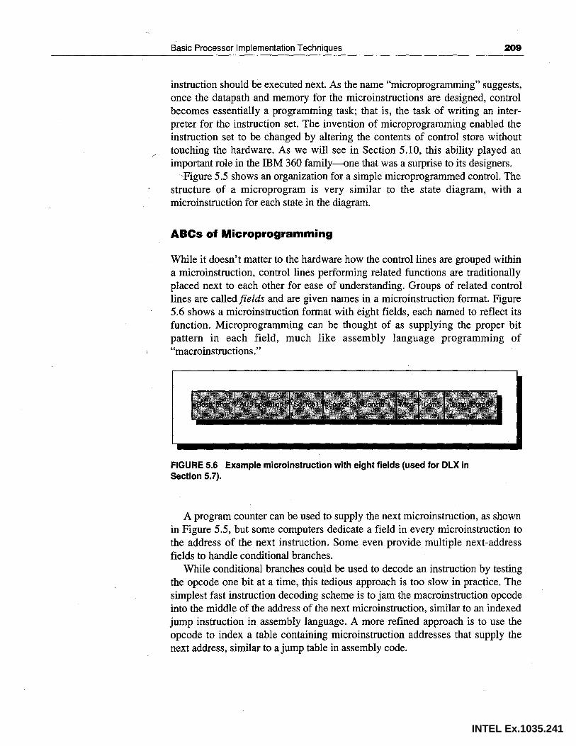
Basic Processor Implementation Techniques 209
instruction should be executed next. As the name "microprogramming" suggests, once the datapath and memory for the microinstructions are designed, control becomes essentially a programming task; that is, the task of writing an interpreter for the instruction set. The invention of microprogramming enabled the instruction set to be changed by altering the contents of control store without touching the hardware. As we will see in Section 5.10, this ability played an important role in the IBM 360 family-one that was a surprise to its designers.
,Figure 5 .5 shows an organization for a simple microprogrammed control. The structure of a microprogram is very similar to the state diagram, with a microinstruction for each state in the diagram.
ABCs of Microprogramming
While it doesn't matter to the hardware how the control lines are grouped within a microinstruction, control lines performing related functions are traditionally placed next to each other for ease of understanding. Groups of related control lines are calledfields and are given names in a microinstruction format. Figure 5.6 shows a microinstruction format with eight fields, each named to reflect its function. Microprogramming can be thought of as supplying the proper bit pattern in each field, much like assembly language programming of "macroinstructions."
FIGURE 5.6 Example microinstruction with eight fields (used for DLX in Section 5. 7).
A program counter can be used to supply the next microinstruction, as shown in Figure 5.5, but some computers dedicate a field in every microinstruction to the address of the next instruction. Some even provide multiple next-address fields to handle conditional branches.
While conditional branches could be used to decode an instruction by testing the opcode one bit at a time, this tedious approach is too slow in practice. The simplest fast instruction decoding scheme is to jam the macroinstruction opcode into the middle of the address of the next microinstruction, similar to an indexed jump instruction in assembly language. A more refined approach is to use the opcode to index a table containing microinstruction addresses that supply the next address, similar to a jump table in assembly code.
INTEL Ex.1035.241

210 5.5 Microprogrammed Control
The microprogram memory, or control store, is the most visible and easily measured hardware in microprogrammed control; hence, it is the focus of techniques to reduce hardware costs. Techniques to trim control-store size include reducing the number of microinstructions, reducing the width of each microinstruction, or both. Just as cost is traditionally measured by control-store size, performance is traditionally measured by .CPI. The wise microprogrammer knows the frequency of macroinstructions by using statistics like those in Chapter 4, and hence knows where and how time is best spent-instructions demanding the largest part of execution time are optimized for speed, and the others are optimized for space.
In four decades of microprogramming history there have been a wide variety of terms and techniques for microprogramming. In fact, a workshop has met annually on this subject since 1968. Before looking at a few examples, let us remember that control techniques-whether hardwired or microcoded-are judged by their impact on hardware cost, clock cycle time, CPI, and
') development time. In the next two sections we will examine how hardware costs can be lowered by reducing control-store size. First we look at two techniques to . reduce the width of microinstructions, then one technique to reduce the number of microinstructions.
Reducing Hardware Costs by Encoding Control Lines
The ideal approach to reducing control store is to first write the complete microprogram in a symbolic notation and then measure how control lines are set in each microinstruction. By taking measurements we are able to recognize control bits that can be encoded into a smaller field. If no more than one of, say, 8 lines is set simultaneously in the same microinstruction, then they can be encoded into a 3-bit field (log2 8 = 3). This change saves 5 bits in every microinstruction and does not hurt CPI, though it does mean the extra hardware cost of a 3-to-8 decoder needed to generate the original 8 control lines. Nevertheless, shaving 5 bits off control-store width will usually overcome the cost of the decoder.
This technique of reducing field width is called encoding. To further save space, control lines may be encoded together if they are only occasionally set in the same microinstruction; two microinstructions instead of one are then required when both must be set. As long as this doesn't happen in critical routines, the narrower microinstruction may justify a few extra words of control store.
There are dangers to encoding. For example, if an encoded control line is on the critical timing path, or if the hardware it controls is on the critical path, then the clock cycle time will suffer. A more subtle danger is that a later revision of the microcode might encounter situations where control lines would be set in the same microinstruction, either hurting performance or requiring changes to the hardware that could lengthen the development cycle.
INTEL Ex.1035.242

Example
Answer
Basic Processor Implementation Techniques 211
Assume we want to encode the three fields that specify a register on a busDestination, Sourcel, and Source2-in the DLX microinstruction format in Figure 5.6. How many bits of control store can be saved versus unencoded fields?
Figure 5.7 lists the registers for each source and destination of the datapath in· Figure 5.1(page200). Note that the destination field must be able to specify that nothing is modified. Without encoding, the 3 fields require 7 + 9 + 9, or 25 bits. Since log2 7 ,,,. 2.8 and log2 9 ,,,. 3.2, the encoded fields require 3 + 4 + 4, or 11 bits. Thus, encoding these 3 fields saves 14 bits per microinstruction.
Number Destination Sourcel/Source2
0 (None) A!B
1 c Temp
2 Temp PC
3 PC IAR
4 IAR MAR
5 MAR MDR
6 MDR IR (16-bit imm)
7 --- IR (26-bit imm)
8 --- Constant
FIGURE 5.7 The sources and destinations specified in the three fields of Figure 5.6 from the datapath description in Figure 5.1. A and B are not separate entries because A can only transfer on the S1 bus and B can only transfer on the S2 bus (see Figure 5.1 on pages 200-201 ). The last entry in the third column, Constant, is used by control to specify a constant needed in an ALU operation (e.g., 4). See Section 5.7 for its use.
Reducing Hardware Costs with Multiple Microinstruction Formats
Microinstructions can be made narrower still if they are broken into different formats and given an opcode or format field to distinguish them. The format field gives all the unspecified control lines their default values, so as not to change anything else in the machine, and is similar to the opcode of a macroinstruction.
Reducing hardware costs by using format fields has its own performance cost-namely, executing more microinstructions. Generally, a microprogram using a single microinstruction format can specify any combination of operations in a datapath and will take fewer clock cycles than a microprogram made up of restricted microinstructions. Narrower machines are cheaper because memory chips are also narrow and tall: It takes many fewer chips for a 16K word by 24-bit memory than for a 4K word by 96-bit memory. (When control memory is on the processor chip, this hardware advantage_ is no longer true.)
INTEL Ex.1035.243

212 5.5 Microprogrammed Control
This narrow but tall approach is often called vertical microcode, while the wide but short approach is called horizontal microcode. It should be noted that the terms "vertical miocrocode" and "horizontal microcode" have no universal definition-the designers of the 8086 considered its 21-bit microinstruction to be more horizontal than other single-chip computers of the time. The related terms maximally encoded and minimally encoded lead to less confusion.
Figure 5.8 plots control-store size against microinstruction width for three ,,.. families of computers. Notice that for each family the total size is similar, even though the width varies by a factor of 6. As a rule, minimally encoded control stores use more bits, and the narrow but tall aspect of memory chips means that maximally encoded control stores naturally have more entries. Sometimes designers of minimally encoded machines don't have the option of shorter RAM chips, causing wide microinstruction machines to end up with many words of control store. Since the hardware costs are not lower if microcode doesn't use up all the space in control store, machines in this class can end up with much larger ) control stores than expected from other implementations. The ECL RAMs available to build the VAX 8800, for example, led to 2000 K bits of control store.
750
500
400
Control store size (Kbits) 300
200
100
0 20 40 60 80 100 120
Microinstruction width (bits)
FIGURE 5.8 Size of control store versus width of microinstructions for 11 computer models. Each point is identified by the length and width of control store (not including parity). Models selected from each family are ones that shipped about tlie same time: IBM 360 models 30, 40, 50, and 65 all shipped in 1965; IBM 370 models 145, 155, and 165 shipped in 1971, with the 135 following in the next year; and the VAX model 780 was shipped in 1978, followed by the 750 in 1980 and the 730 in 1982. The development of the VAX designs all overlapped one another inside DEC.
INTEL Ex.1035.244

Basic Processor Implementation Techniques
Reducing Hardware Costs by Adding Hardwired Control to Share Microcode
213
The other approach to reducing control store is to reduce the number of microinstructions rather than their width. Microsubroutines provide one approach, as well as routines with common "tail" sequences sharing code by jumps.
More sharing can be done with hardwired control assistance. For example, many microarchitectures allow bits of the instruction register to specify the correct register. Another common assist is to use portions of the instruction register to specify the ALU operation. Each of these assists is undei: microprogrammed control and is invoked with a special value in the appropriate field. The 8086 uses both techniques, giving one 4-line routine responsibility for 32 opcodes. The drawback of adding hardwired control is it may stretch the development cycle because it no longer involves programming, but requires hardware layout for designing and debugging.
This section and the previous two give techniques for reducing cost. The following sections present three techniques for improving performance.
Reducing CPI with Special Case Microcode
As we have noted, the wise microprogrammer knows when to save space and when to spend it. An instance of this is dedicating extra microcode for frequent instructions, thereby reducing CPI. For example, the VAX 8800 uses its large control store for many versions of the CALLS instruction, optimized for register saving depending upon the value in the register-save mask. Candidates for special case microcode can be uncovered by instruction mix measurements, such as those found in Chapter 4 or in Appendix B, or by counting the frequency of use of each microinstruction in an existing implementation (see Erner and Clark [1984]).
Reducing CPI by Adding Hardwired Control
Adding hardwired control can reduce costs as well as improve performance. For example, VAX operands can be in memory or registers, but later machines reduce CPI by having special code for register-register or register-memory moves and adds: ADDL2 Rn, 10 (Rm) takes five or more cycles on the 780, but as few as one on the 8600. Another example is in the memory interface, where the straightforward solution is for microcode to continuously test and branch until memory is ready. Because of the delay between the time a condition becomes true and the time the next microinstruction is read, this approach can add one extra clock to each memory access. The importance of the memory interface is underlined by the 780 and 8800 statistics-20% of the 780 clock cycles and 23% of the 8800 are waiting for memory to be ready, these are called
INTEL Ex.1035.245

214
5.6 J
5.5 Microprogrammed Control
stalls. A stall is where an instruction must pause one or more clock cycles waiting for some resource to be available. In this chapter stalls occur only when waiting for memory; in the next chapter we '11 see other reasons for stalls.
Many machines approach this problem by having the hardware stall a microinstruction that tries to access the memory-data register before the memory operation is completed: (This can be accomplished by freezing the microinstruction address so that the same microinstruction is executed until the condition is met.) The instant the memory reference is ready, the microinstruction that needs the data is allowed to complete, avoiding the extra clock delay to access control memory.
Reducing CPI by Parallelism
Sometimes CPI can be reduced with more operations per microinstruction. This technique, which usually requires a wider microinstruction, increases parallelism with more datapath operations. It is another characteristic of machines labeled horizontal. Examples of this performance gain can be seen in the fact that the fastest models of each family in Figure 5.8 also have the widest microinstructions. Making the microinstruction wider does not guarantee increased performance, however. An example where the potential gain was not realized is found in a microprocessor very similar to the 8086, except that another bus was added to the datapath, requiring six more bits in its microinstruction. This could have reduced the execution phase from three clock cycles to two for many popular 8086 instructions. Unfortunately, these popular macroinstructions were grouped with macroinstructions that couldn't take advantage of this optimization, so they all had to run at the slower rate.
Interrupts and Other Entanglements
Control is the hard part of processor design, and the hard part of control is interrupts-events other than branches that change the normal flow of instruction execution. Detecting interrupt conditions within an instruction can often be on the critical timing path of a machine, possibly affecting the clock cycle time, and thus performance. Without proper attention to interrupts during design, adding interrupts to a complicated implementation can even foul up the works so as to make the design impracticable.
Invented to detect arithmetic errors and signal real-time events, interrupts have been handed a flock of difficult duties. Here are 11 examples:
I/0 device request
Invoking an operating system service from a user program
Tracing instruction execution
INTEL Ex.1035.246

I/O device request
Invoking the operat-ing system service from a user proJl;ram
Tracing instruction execution Breakpoint
Arithmetic overflow or underflow
Page fault (not in main memory)
Misaligned memory accesses
Memory protection violations
Using undefined instructions
Hardware malfunctions
Power failure
Basic Processor Implementation Techniques
Breakpoint (programmer-requested interrupt)
Arithmetic overflow or underflow
Page fault (not in main memory)
Misaligned memory accesses (if alignment is required)
Memory-protection violation
Using an undefined instruction
Hardware malfunctions
Power failure
IBM360 VAX Motorola 680x0
Input/output Device interrupt Exception (Level interruption 0 ... 7 autovector)
Supervisor call Exception (change Exception interruption mode supervisor trap) (unimplemented
instruction)--on - Macintosh
NA Exception (trace Exception (trace) fault)
NA Exception Exception (illegal (breakpoint fault) instruction or
breakpoint)
Program interruption Exception (integer Exception (overflow or overflow trap or (floating-point underflow exception) floating underflow coprocessor errors)
fault)
NA (only in 370) Exception Exception (memory-(translation not valid management unit fault) errors)
Program interruption NA Exception (specification (address error) exception)
Program interruption Exception (access Exception (protection control violation (bus error) exception) fault)
Program interruption Exception (opcode Exception (illegal (operation exception) privileged/ instruction or break-
reserved fault) point/unimplemented instruction)
Machine-check Exception (machine- Exception interruption check abort) (bus error)
Machine-check Urgent interrupt NA interruption
215
Intel 80x86
Vectored interrupt
Interrupt (INT instruction)
Interrupt (single-step trap)
Interrupt (breakpoint trap)
Interrupt (overflow trap or math unit exception)
Interrupt (page.fault)-
NA
Interrupt (protection exception)
Interrupt (invalid opcode)
NA
Nonmaskable interrupt
FIGURE 5.9 Names of 11 interrupt classes on four computers. Every event on the IBM 360 and 80x86 is called an interrupt, while every event on the 680x0 is called an exception. VAX divides events into interrupts or exceptions. Adjectives device, software, and urgent are used with VAX interrupts, while VAX exceptions are subdivided into faults, traps, and aborts.
INTEL Ex.1035.247

216 5.6 Interrupts and Other Entanglements
The enlarged responsibility of interrupts has led to the confusing situation of each computer vendor inventing a different term for the same event, as Figure 5.9 on page 215 illustrates. Intel and IBM still call such events interrupts, but Motorola calls them exceptions; and, depending on the circumstances, DEC calls them exceptions, faults, aborts, traps, or interrupts. To give some idea of how often interrupts occur, Figure 5.10 shows the frequency on the VAX 8800.
Event Time between events
I/O interrupt 2.7ms
Interval timer interrupt 10.0 ms
Software interrupt 1.5 ms
Any interrupt 0.9ms
Any hardware interrupt 2.1 ms
FIGURE 5.10 Frequency of different interrupts on the VAX 8800 running a multiuser workload on the VMS timesharing system. Real-time operating systems used in embedded controllers may have a higher interrupt rate than a general-purpose timesharing system. (Collected by Clark, Bannon, and Keller [1988].)
Clearly, there is no consistent convention for naming these events. Rather than imposing one, then, let's review the reasons for the different names. The events can be characterized on five independent axes:
1. Synchronous versus asynchronous. If the event occurs at the same place every time the program is executed with the same data and memory allocation, the event is synchronous. With the exception of hardware malfunctions, asynchronous events are caused by devices external to the processor and memory.
2. User request versus coerced. If the user task directly asks for it, it is a userrequest event.
3. User maskable versus user nonmaskable. If it can be masked or disabled by a user task, the event is user maskable.
4. Within versus between instructions. This classification depends on whether the event prevents instruction completion by occurring in the middle of execution-no matter how short-or whether it is recognized between instructions.
5. Resume versus terminate. If the program's execution stops after the interrupt, it is a terminating event.
INTEL Ex.1035.248

r
I/0 device request
Invoking operating system service
Basic Processor Implementation Techniques 217
The difficult task is implementing interrupts occurring within instructions where the instruction must be resumed. Another program must be invoked to collect the state of the program, correct the cause of an interrupt, and then restore the state of the program before an instruction can be tried again.
Figure 5.11 classifies the examples from Figure 5.9 according to these five categories.
·.
Synchronous vs. User User Within vs. Resume vs. asynchronous request vs. maskable vs. between terminate
coerced nonmaskable instructions
Asynchronous Coerced Nonmaskable Between Resume
Synchronous User request Nonmaskable Between Resume
Tracing instruction execution Synchronous User request User maskable Between Resume
Breakpoint Synchronous User request User maskable Between Resume
Integer arithmetic overflow Synchronous Coerced User maskable Within Terminate
Floating-point arithmetic - Synchronous Coerced User maskable Within Resume overflow or underflow
Page fault Synchronous Coerced Nonmaskable Within Resume
Misaligned memory accesses Synchronous Coerced User maskable Within Terminate
Memory-protection violations Synchronous Coerced Nonmaskable Within Terminate
Using undefined instructions Synchronous Coerced Nonmaskable Within Terminate
Hardware malfunctions Asynchronous Coerced Nonmaskable Within Terminate
Power failure Asynchronous Coerced Nonmaskable Within Terminate
FIGURE 5.11 The events of Figure 5.9 classified using five categories.
How Control Checks for Interrupts
Integrating interrupts with control means modifying the finite-state diagram to check for interrupts. Interrupts that occur between instructions are checked either at the beginning of the finite-state diagram-before an instruction is decoded-or at the end-after the execution of an instruction is completed. Interrupts that can occur within an instruction are generally detected in the state that causes the action or in a state that follows it. For example, Figure 5.12 shows Figure 5 .4 (page 207) modified to check for interrupts:
We assume DLX transfers the return address into a new programmer-visible register, the interrupt return-address register. Control then loads PC with the address of the interrupt routine for that interrupt.
INTEL Ex.1035.249

218 5.6 Interrupts and Other Entanglements
Memory access not complete (no interrupt)
Memory access complete (no page fault)
FIGURE 5.12 The top-level view of the DLX finite-state diagram (Figure 5.4 on page 207) modified to check for interrupts. Either a between interrupt or an instruction page fault invokes the control that saves the PC and then loads it with the address of the appropriate interrupt routine. The lower portion of the figure shows interrupts resulting in page faults of data accesses or arithm~tic overflow.
What's Hard About lllterrupts
The conflicting terminology is confusing, but that is not what makes the hard part of control hard. Even though interrupts are rare, the hardware must be designed so that the full state of the machine can be saved, including an indication of the offending event, and the PC of the instruction to be executed after the interrupt is serviced. This difficulty is exacerbated by events occurring during the middle of execution, for many instructions also require the hardware to restore the machine to the sta,te just before the event occurred-the beginning of the instruction. This last requirement is so difficult that computers are awarded the title restartable if they pass that test. That supercomputers and many early microprocessors do not earn that badge of honor illustrates both the difficulty of interrupts and the potential cost in hardware complexity and execution speed.
No engineers deserve more admiration than those who built the first VAX, DEC's first restartable minicomputer. The variable-length instructions mean the comp~ter can fetch 50 bytes of one instruction before discovering that the next
INTEL Ex.1035.250

Basic Processor Implementation Techniques 219
byte of the instruction is not in main memory-a situation that requires the saved PC to point 50 bytes earlier. Imagine the difficulties of restarting an instruction with six operands, each of which could be misaligned and thus be partially in memory and partially on disk!
The instructions that are hardest to restart are those that modify some of the machine state before it is known whether interrupts can occur. The VAX autoincrement and autodecrement addressing modes would naturally modify
· registers during the addressing phase of execution rather than at the writeback phase, and so would be vulnerable to this difficulty. To avoid this problem, recent VAXes keep a history queue of the register specifiers and the operations on the registers, so that the operations can be reversed on an interrupt. Another approach, used on the earlier VAXes, is to record the specifiers and the original values of the registers, restoring the original values on interrupt. (The primary difference is that it only takes a few bits to record how the address was changed due to autoincrement or autodecrement versus the full 32-bit register value.)
It is not just addressing modes that make the VAX difficult to restart; longrunning instructions mean that interrupts must be checked in the middle of execution to prevent long interrupt latency. MOVC3, for example, copies up to 216 bytes and can take tens of milliseconds to finish-far too long to wait for an urgent event. On the other hand, even if there were a way to undo copying in the middle of execution so that MOVC 3 could be restarted, interrupts would occur so frequently, relative to this long-running instruction (see Figure 5.10 on page 216), that MOVC3 would be restarted repeatedly under those conditions. Such wasted effort from incomplete copies would render MOVC 3 worse than useless.
DEC divided the problem to conquer it. First, the operands-source address, length, and destination address-are fetched from memory and placed into general-purpose registers Rl, R2, and R3. If an interrupt occurs during this first phase, these registers are restored, and the MOVC 3 is restarted from scratch. After this first phase, every time a byte is copied, the length (R2) is decremented and addresses (Rl and R3) are incremented. If an interrupt occurs during this second phase, MOVC 3 sets the first part done (FPD) bit in the program status word. When the interrupt is serviced and the instruction is reexecuted, it first checks the FPD bit to see if the operands have already been placed in registers. If so, the VAX doesn't fetch the address and length operands, but just continues with the current values in the registers, since that is all that remains to be copied. This permits more rapid response to interrupts while allowing long-running instructions to make progress between interrupts.
IBM had a similar problem. The 360 included the MVC instruction, which copies up to 256 bytes of data. For the early machines without virtual memory, the machine simply waited until the instruction was completed before servicing interrupts. With the inclusion of virtual memory in the 370, the problem could no longer be ignored. Control first tries to access all possible pages, forcing all possible virtual memory miss interrupts to occur before moving any data. If any interrupts occur in this phase, the instruction is restarted. Control then ignores interrupts until the instruction is complete. To allow longer copies, the 370
INTEL Ex.1035.251

220 5.6 Interrupts and Other Entanglements
includes MVCL, which can move up to 224 bytes. The operands are in registers and are updated as a part of execution-like the VAX, except that there is no need for FPD since the operands are always in registers. (Or, to speak historically, the VAX solution is like the IBM 370, which came first.)
5. 7 I Putting It All Together: Control for DLX
The control for DLX is presented here to tie together the ideas from the previous three sections. We begin with a finite-state diagram to represent hardwired control and end with microprogrammed control. Both versions of DLX control are used to demonstrate tradeoffs to reduce cost or to improve performance. Because the figures are already too large, the checking for data page faults or arithmetic overflow shown in Figure 5.12 (page 218) is not included in this section. (Exercise 5.12 adds them.)
Data transfer (Figure 5.14)
Memory access not complete
l.
ALU (Figure 5.15)
access complete
Set (Figure 5.16)
Jump (Figure 5.17)
Branch (Figure 5.18)
FIGURE 5.13 The top-level view of the DLX finite-state diagram for the non-floatingpoint instructions. The first two steps of instruction execution-instruction fetch and instruction decode/register fetch-are shown. The first state repeats until the instruction is fetched from memory or an interrupt is detected. If an interrupt is detected, the PC is saved in IAR and PC is set to the address of the interrupt routine. The last three steps of instruction execution-execution/effective address, memory access, and write back-are shown in Figures 5.14 to 5.18 on pages 221-224.
INTEL Ex.1035.252

I Data transfer
l MOVS21
MOVl2S
Basic Processor Implementation Techniques 221
Rather than trying to draw. the DLX finite-state machine in a single figure showing all 52 states, Figure 5.13 (see page 220) shows just the top level, containing 4 states plus references to the rest of the states detailed in Figures 5.14 (below) through 5.18 (page 224). Unlike Figure 5.2 (page 205), Figure 5.13 takes advantage of the change to the datapath allowing PC to address memory directly without going through MAR (Figure 5.4 on page 207).
Memory
Figure 5.13
access complete
FIGURE 5.14 The effective address calculation, memory-access, and write-back states for the memory-access and data-transfer instructions of DLX. For loads, the second state repeats until the data is fetched from memory. The final state of stores repeats until the write is complete. While the operation of all five loads is shown in the states of this figure, the proper operation of writes depends on the memory system writing bytes and halfwords, without disturbing the rest of the word in memory, and correctly aligning the bytes and halfwords (see Figure 3.10, page 97) over the proper bytes of memory. On completion of execution control transfers to Figure 5.13, found on page 220.
INTEL Ex.1035.253

222 5.7 Putting It All Together: Control for DLX
ALU
ADD! AND! OR !
Figure 5.13
FIGURE 5.15 The execution and write-back states for the ALU instructions of DLX. After putting a register or the sign-extended 16-bit immediate into Temp, 1 of the 9 instructions is executed, and the result (C) is written back into the register file. Only SRA and LHI may not be self-explanatory: The SRA instruction shifts right while it sign extends the operand and LHI loads the upper 16 bits of the register while zeroing the lower 16 bits. (The C operators « and » shift left and right, respectively; they fill with zeros unless bits are concatenated explicitly using##, e.g., sign extension). As mentioned above, the check for overflow in ADD and SUB is not included to simplify the figure. On completion of execution control transfers to Figure 5.13 (page 220).
FIGURE 5.16 (See adjoining page.) The execution and write-back states for the Set instructions of DLX. After putting a register or the sign-extended 16-bit immediate into Temp, 1 of the 6 instructions compares A to Temp and then sets C to 1 or 0, depending on whether the condition is true or false. C is then written back into the register file, and then execution control transfers to Figure 5.13 (page 220). The dashed lines in this figure and Figure 5.18 are used to make it easier to follow intersecting lines.
FIGURE 5.17 (See adjoining page.) The execution and write-back states for the jump instructions of DLX. With jump and link instructions, the return address is first placed in C before the new value is loaded into PC. Trap saves it in IAR. Note that the immediate in these instructions is 1 O bits longer than the 16-bit immediate in all other instructions. Jump and link instructions conclude by writing the return address back into R31. On completion of execution, control transfers to Figure 5.13 (page 220).
INTEL Ex.1035.254

Basic Processor Implementation Techniques 223
Figure 5.13
FIGURE 5.16
FIGURES.17
INTEL Ex.1035.255

224
Example
Answer
5.7 Putting It All Together: Control for DLX
Branch
I\~ y~
·." Figure 5.13
FIGURE 5.18 The execution states for the branch instructions of DLX. The PC is loaded with the sum of the PC and the immediate only if the condition is true. On completion of execution, control transfers to Figure 5.13, found on page 220.
Performance of Hardwired Control for DLX
As stated in Section 5.4, the goal for control designs is to minimize CPI, clock cycle time, amount of control hardware, and development time. CPI is just the average number of states along the execution path of an instruction.
Let's assume thathardwired control directly implements the finite-state diagram in Figures 5.13 to 5.18. What is the CPI for DLX running GCC?
The number of clock cycles to execute each DLX instruction is determined by simply counting the states of an instruction. Starting at the top, every instruction spends at least two clock cycles in the states in Figure 5.13 (ignoring interrupts). The actual number depends on the average number of times the state accessing· memory must repeat because· memory is not ready. (These wasted clock cycles are usually c~lled memory stall cycles or wait states.) In cache-based machines this value is typically 0 (i.e., no repetitions since cache access is 1 cycle) when the data is found in the cache, and 10 or higher when it is not ..
The time for the remaining portion of instruction execution comes from the additional figures. Besides two cycles for fetch and decode, loads take four more cycles plus clock cycles waiting for the data access, while stores take just three more clock cycles plus wait states. Three extra clock cycles are also needed by ALU instructions, and set instructions take four. Figure 5.17 shows that jumps take just one extra clock cycle with jump and links taking three. Branches depend on the result: Taken branches use two more clock cycles while
INTEL Ex.1035.256

Basic Processor Implementation Techniques 225
DLX instructions Minimum Memory Total clock clock cycles accesses cycles
Loads 6 2 8
Stores 5 2 7
ALU 5 1 6
Set 6 1 7
Jumps 3 1 4
Jump and links 5 1 6
Branch (taken) 4 1 5
Branch (not taken) 3 1 4
FIGURE 5.19 Clock cycles per instruction for DLX categories using the state diagram in Figures 5.13 through 5.18. Determining the total clock cycles per category requires multiplying the number of memory accesses-including instruction fetches-times the average number of wait states, and adding this product to the minimum number of clock cycles. We assume an average of 1 clock cycle per memory access. For example, loads take eight clock cycles if the average number of wait states is one.
untaken branches need just one. Adding these times to the first portion of instruction execution yields the clock cycles per DLX instruction class shown in Figure 5.19.
From Chapter 2, one way to calculate CPI is
n
CPI = ~(CPI· * ~i ) ,£..J 1 Instruction count i=l
Using the DLX instruction mix from Figure C.4 in Appendix C for GCC (normalized to 100% ), the percentage of taken branches from Figure 3.22 (page 107), and one for the average number of wait states per memory access, the DLX CPI for this datapath and state diagram is calculated:
Loads 8 * 21% = 1.68
Stores 7 * 12% = 0.84
ALU 6 * 37% = 2.22
Set 7 * 6% = 0.42
Jumps 4 * 2% = 0.08
Jump and links 6 * 0% = 0.00
Branch (taken) 5 * 12% = 0.60
Branch (not taken) 4 * 11% = 0.44
Total CPI: 6.28
Thus, the DLX CPI for GCC is about 6.3.
INTEL Ex.1035.257

226
Example
Answer
5.7 Putting It All Together: Control for DLX
Improving DLX Performance When Control Is Hardwired
As mentioned above, performance is improved by reducing the number of states an instruction must pass through during execution. Sometimes, performance can be improved by removing intermediate calculations that select one of several options, either by adding hardware that uses information in the opcode to later select the appropriate option, or by simply increasing the number of states.
Let's look at improving the performance of ALU instructions by removing the top two states in Figure 5.15 on page 222, which load either a register or an immediate into Temp. One approach uses a new hardware option. Let's call it "X" (see Figure 5.20). The X option selects either the B register or the 16-bit immediate, depending on the opcode in IR. A second approach is simply to increase the number of execution states so that there are separate states for ALU instructions usii;ig immediate versus ALU instructions using registers.
For each option, what would be the change in performance, and how should the state diagram be changed? Also, how many states are needed in each option?
Either change reduces ALU execution time from five to four clock cycles plus wait states. From Figure C.4, ALU operations are about 37% of the instructions for GCC, lowering CPI from 6.3 to 5.9, and making the machine about 7% faster. Figure 5 .20 shows Figure 5 .15 modified to use the X option instead of the two states that load Temp, while Figure 5.21 simply has many more states to achieve the same result. The total number of states are 50 and 58, respectively.
ALU
4711\~ AND j ~=~=""'
SRA i
Figure 5.13
FIGURE 5.20 Figure 5.15 modified to remove the two states loading Temp. The states use the new X option to mean that either B or (IR16) 16##1R16 .. 31 is the operand, depending on the DLX opcode.
INTEL Ex.1035.258

Basic Processor Implementation Techniques 227
ALU
ADDI /
SUB~ /
ANDI /
XORI /
SLLI /
SRLI /
/
Figure 5.13
FIGURE 5.21 Figure 5.15 modified to remove the two states loading Temp. Unlike Figure 5.20, this requires no new hardware options in the datapath, but simply more control states.
Control can affect the clock cycle time, either because control itself takes longer than the corresponding operations in the datapath, or because the datapath operations selected by control lengthens the worst-case clock cycle time.
INTEL Ex.1035.259

228
Example
Answer
5.7 Putting It All Together: Control for DLX
Assume a machine with a 10-ns clock cycle (100-MHz clock rate). Suppose that on closer inspection the designer discovered that all states could be executed in 9 ns, except states that use the shifter. Would it be wise to split those states, taking two 9-ns clock cycles for shift states and one 9-ns clock for everything else?
Assuming the improvement in the previous example, the average instruction execution time for the 100-MHz machine is 5.9*10 ns or 59 ns. The shifter is only used in the states of four instructions: SLL, SRL, SRA, and LHI (see Figure 5.20). In fact, each of these instructions takes 5 clock cycles (including one wait state for memory access), and only one of the five original clock cycles need be split into two new clock cycles. Thus, the average execution time of these instructions changes from 5* 10 ns, or 50 ns, to 6*9 ns, or 54 ns. From Figure C.4 these 4 instructions are about 11 % of the instructions executed for GCC (after normalization), making the average instruction execution time 89% * (5.9*9 ns) + 11 %*54 ns or 53 ns. Thus, splitting the shift state results in a machine that is about 10% faster-a wise decision. (See Exercise 5.8 for a more sophisticated version of this tradeoff.)
Hardwired control is completed by listing the control signals activated in each state, assigning numbers to the states, and finally generating the PLA. Now let's implement control using microcode in a ROM.
Microcoded Control for DLX
A custom format such as this is a slave to the architecture of the hardware and instruction set which it serves. The format must strike a proper compromise between ROM size, ROM-output decoding circuitry size, and machine execution rate.
Jim McKevit et al. [ 1977]
Before microprogramming can commence, the microinstruction set must be determined. The first step is to list the possible entries for each field of the DLX microinstruction format from Figure 5.6 on page 209. Figure 5.7 on page 211
. lists them for the Destination, Sourcel, and Source2 fields. Figure 5.22 below shows the values for the remaining fields.
Sequencing of microinstructions i:equires further explanation. The microprogrammed control includes a microprogram counter to specify th€ address of the next microinstruction if a branch is not taken, as in Figu_re 5.5 on page 208. In addition to the branches using the Jump address field, three tables are used to decode the DLX macroinstructions. These tables are indexed with the opcodes of the DLX instruction, and supply a microprogram address depending on the value in the opcode. Their use will become clear as we examine the DLX micr_oprogram.
INTEL Ex.1035.260

Basic Processor Implementation Techniques 229
Value ALU Misc Cond
0 ADD + Instr Read /Rf- - - - Go to next sequential microinstruction M[PC]
1 SUB - DataRead MDRf- Uncond Always jump M[MAR]
2 RSUB -r Write M[MAR]f- Int? Pending (between instruction) interrupt?
(reverse sub) MDR
3 AND & ABf-RF LoadA&B Mem? Memory access not complete? from Reg. File
4 OR I Rdf-C Write Rd Zero? Is the ALU output zero?
5 XOR /\ R31f-C Write R31 Negative? ls the ALU output less than zero? J',
(for call)
6 SLL << Load? Is the macroinstruction a DI.x load?
7 SRL >> Decodel Address table 1 determines next micro-(Fig. 5.24) instruction (uses main opcode)
8 SRA >>a Decode2 Address table 2 determines next micro-(Fig. 5.26) instruction (uses ''func" opcode)
9 Pass Sl SJ Decode3 Address table 3 determines next micro-(Fig. 5.26) instruction (uses main opcode)
10 Pass S2 S2
FIGURE 5.22 The options for three fields of the DLX microinstruction format in Figure 5.6 on page 209. The possible names are shown on the left of the field name, with an explanation of each field to the right. The real microinstruction would contain a bit pattern corresponding to the number in the first column. Combined with Figure 5. 7 (page 211 ), all the fields are defined except the Constant and Jump address fields, which contain numbers supplied by the microprogrammer. »a is an abbreviation for shift right arithmetic and -,means reverse subtract (B -,A= A- B).
Following the lead of the state diagram, the DLX microprogram is divided into Figures 5.23, 5.25, 5.27, 5.28, and 5.29, with each section of microcode corresponding to one of Figures 5.13 to 5.18 (pages 220-224). The first state in Figure 5.13 becomes the first two microinstructions in Figure 5.23. The first microinstruction (address 0) branches to microinstruction 3 if there is an interrupt pending. Microinstruction 1 fetches an instruction from memory, branching back to itself as long as the memory access is not complete. Microinstruction 2 increments the PC by 4, loads A and B, and then does the first-level decoding. The address of the next microinstruction then depends on which macroinstruction is in the instruction register. The microinstruction addresses for this first-level macroinstruction decode are specified in Figure 5.24. (In reality, the table shown in this figure is specified after the microprogram is written, as both the number of entries and the corresponding locations aren't known until then.)
INTEL Ex.1035.261

230 5.7 Putting It All Together: Control for DLX
Loe Label Dest ALU Sl S2 c Misc Cond Jump Comment label
0 If etch: Interrupt? Intrpt Check interrupt
1 Hoop: Instr Read Mem? Hoop IR <:-M[PC]; wait for memory
2 PC ADD PC Constant 4 AB<:-RF Decodel
3 Intrpt: IAR Pass Sl PC Interrupt
4 PC Pass S2 Constant 0 Uncond If etch PC<:-0 & go fetch next instruction
FIGURE 5.23 The first section of the DLX microprogram, corresponding to the states in Figure 5.13 (page 220). The first column contains the absolute address of the microinstruction, followed by a label. The rest of the fields contain values from Figures 5. 7 (page 211) and 5.22 for the microinstruction format in Figure 5.6 (page 209). As an example, microinstruction 2 corresponds to the second state of Figure 5.13. It sends the output from the ALU into PC, tells the ALU to add, puts PC onto the Source1 bus, and a constant from the microinstruction (whose value is 4) onto the Source2 bus. In addition, A and Bare loaded from the register file according to the specifiers in IR. Finally, the address of the next microinstruction to be executed comes from decode table 1 (Figure 5.24), which depends on the opcode· in the instruction register (IR).
Opcodes (symbolically Absolute Label Figure specified) address
Memory 5 Mem: 5.25
Move to special 20 Movl2S: 5.25
Move from special 21 MovS2I: 5.25
S2=B 23 Reg: 5.27
S2 = Immediate 24 Imm: S.27
Branch equal zero 50 Beq: 5.29
Branch not equal zero 52 Bne: 5.29
Jump 54 Jump: 5.29
Jump register 55 JReg: 5.29
Jump and link 56 JAL: 5.29
Jump and link register 58 JALR: 5.29
Trap 60 Trap: 5.29
FIGURE 5.24 Opcodes and corresponding addresses for decode table 1. The opcodes are shown symbolically on the left, followed by the addresses with the absolute microinstruction address, a label, and the figure where the microcode can be found. If this table were implemented with a ROM it would contain 64 entries corresponding to the 6-bit opcode of DLX. As this would clearly result in many redundant or unspecified entries, a PLA could be used to minimize hardware.
Figure 5.25 contains the DLX load and store instructions. Microinstruction 5 calculates the effective address, and branches to microinstruction 9 if the
INTEL Ex.1035.262
f',
Loe Label Dest
5 Mem: MAR
6 Store: MDR 7 Dloop:
8 9 Load:
IO 11 LB: Temp
I2 c
13 LBU: Temp
14 c IS LH: Temp
I6 c 17 LHU: Temp
18 c I9 LW: c 20 Movl2S: IAR 21 MovS21: c 22 Write I:
Basic Processor Implementation Techniques 231
macroinstruction in the IR is a load. If not, microinstruction 6 loads MDR with the value to be stored, and microinstruction 7 jumps to itself until the memory is finished writing the data. Microinstruction 8 then jumps back to microinstruction 0 (Figure 5.23) to begin the execution cycle all over again. If the macroinstruction was a load, microinstruction 9 loops until the data has been read. Microinstruction 10 then uses decode table 2 (specified in Figure 5.26) to specify the address of the next microinstruction. Unlike the first decode table, this table is used by other microinstructions. (There is no conflict in multiple uses since the opcodes for each instance are different.)
Suppose the instruction were load halfword. Figure 5.26 shows that the result of decode 2 would be to jump to microinstruction 15. This microinstruction shifts the contents of MDR to the left 16 bits and stores the result in Temp. The following microinstruction shifts Temp right arithmetically 16 bits and puts the result in C. C now contains the 16 rightmost bits of MDR, with the upper 16 bits containing the extended sign. This microinstruction jumps to location 22, which writes C back into the destination register specifier in IR, and then jumps to fetch the next macroinstruction starting at location 0 (Figure 5.23).
ALU Sl S2 c Misc Cond Jump Comment label
ADD A immI6 Load? Load M emorv instruct.
Pass S2 B Store
Data write Mem? Dloop
Uncond If etch Fetch next instr.
Data read Mem? Load LoadMDR
Decode2 SLL MDR Constant 24 Load byte; shift left to
remove uvver 24 bits
SRA Temp Constant 24 Uncond Write I Shift right arithmetic to sifm extend
SLL MDR Constant 24 LB unsi1med
SRL Temp Constant 24 Uncond Write I Shift rif~ht lof!.ical
SLL MDR Constant I6 Load half
SRA Temp Constant I6 Uncond Write I Shift rif!.ht arithmetic
SLL MDR Constant I6 LH Unsif!.ned
SRL Temp Constant I6 Uncond Write I Shift rif!.ht lof!.ical
Pass Sl MDR Uncond Write I Load word
Pass SI A Uncond If etch Move to special
Pass SI IAR Move from spec.
Rdf--C Uncond If etch Write back & go fetch next instruction
FIGURE 5.25 The section of the DLX microprogram for loads and stores, corresponding to the states in Figure 5.14 (page 221). The microcode for bytes and halfwords takes an extra microinstruction to align the data (see Figure 3.10, page 97). Note that microinstruction 5 loads A from Rd, just in case the instruction is a store. The label lfetch is for microinstruction 0 in Figure 5.23 on page 230.
INTEL Ex.1035.263

232 5.7 Putting It All Together: Control for DLX
Opcode Absolute Label Figure address
Load byte 11 LB: 5.25
Load byte unsigned 13 LBU: 5.25
Load half 15 LH: 5.25
Load half unsigned 17 LHU: 5.25
Load word 19 LW: 5.25
ADD 25 ADD/I: 5.27
SUB 26 SUB/I: 5.27
AND 27 AND/I: 5.27
OR 28 OR/I: 5.27
XOR 29 XOR/I: 5.27
SLL 30 SLL/I: 5.27
SRL 31 SRL/I: 5.27
SRA 32 SRA/I: 5.27
LHI 33 LHI: 5.27
Set equal 35 SEQ/I: 5.28
Set not equal 37 SNEil: 5.28
Set less than 39 SLT/I: 5.28
Set greater than or equal 41 SGE/I: 5.28
Set greater than 43 SGT/I: 5.28
Set less than or equal 45 SLE/I: 5.28
FIGURE 5.26 Opcodes and corresponding addresses for decode tables 2 and 3. The opcodes are shown symbolically on the left, followed by the absolute microinstruction address, the corresponding label, and the figure where the microcode can be found. Since the opcodes are shown symbolically, and they go to the same place in both tables, the same information can be used for specifying decode tables 2 and 3. This similarity is attributable to the immediate version and register version of the DLX instructions sharing the same microcode. If a table were implemented with a ROM, it would contain 64 entries corresponding to the 6-bit opcode of DLX. Again, the many redundant or unspecified entries suggest the use of a PLA to minimize hardware cost.
The ALU instructions are found in Figure 5.27. The first two microinstructions correspond to the states at the top of Figure 5.15 (page 222). After loading .. Temp with either the register or the immediate, each uses a decode table to vector to the microinstruction that executes the ALU instruction. To save microcode space, the same microinstruction is used whether the operand is a register or an immediate. One of the microinstructions between 25 and 33 is executed, storing its result in C. It then jumps to microinstruction 34, which stores C into the register specified in the IR, and in turn jumps to fetch the next macroinstruction.
INTEL Ex.1035.264

Basic Processor Implementation Techniques 233
Loe Label Dest ALU Sl S2 c Misc Cond Jump Comment label
23 Reg: Temp Pass S2 B Decode2 -- source2 = ref!.
24 Imm: Temp Pass S2 Imm Decode3 source2 = imm. 25 ADD/I: c ADD A Temp Uncond Write2 ADD 26 SUB/I: c SUB A Temp Uncond Write2 SUB
27 AND/I: c AND A Temp Uncond Write2 AND 28 OR/I: c OR A Temp Uncond Write2 OR
29 XOR/I: c XOR A Temp Uncond Write2 XOR
30 SLL/I: c SLL A Temp Uncond Write2 SLL
31 SRL/I: c SRL A Temp Uncond Write2 SRL
32 SRA/I: c SRA A Temp Uncond Write2 SRA
33 LHI: c SLL Temp Constant 16 ., Uncond Write2 LHI
34 Write2: Rdf-C Uncond If etch Write back & go fetch next instruction
FIGURE 5.27 .Like the first two states in Figure 5.15 (page 222), microinstructions 23 and 24 load Temp with an operand and then vector to the appropriate microinstruction, depending on the opcode in IR. One of the nine following microinstructions is executed, leaving its result in C. C is written back into the register specified in the register destination field of DLX macroinstruction in IR in microinstruction 34.
Loe Label Dest ALU Sl S2 c Misc Cond Jump' Comment label
35 SEQ/I: SUB A Temp Zero? Setl Set equal
36 c Pass S2 Constant 0 Uncond Write4 AR (set to false)
37 SNE/I: SUB A Temp Zero? Seto Set not equal
38 c Pass S2 Constant 1 Uncond Write4 AR (set to true)
39 SLT/I: SUB A Temp Negative? Setl Set less than
40 c Pass S2 Constant 0 Uncond Write4 A~T (set to false)
41 SGE/I: SUB A Temp Negative? Seto Set GT or equal
42 c Pass S2 Constant 1 Uncond Write4 A~T (set to true)
43 SGT/I: RSUB A Temp Negative? Setl Set weater than
44 c Pass S2 Constant 0 Uncond Write4 T~ (set to false)
45 SLE/I: RSUB A Temp Negative? Seto Set LT or equal
46 c Pass S2 Constant 1 Uncond Write4 T~ (set to true)
47 Seto: c Pass S2 Constant 0 Uncond Write4 Set to 0 =false
48 Setl: c Pass S2 Constant 1 Set to 1 = true
49 Write4: Rdf-C Uncond If etch Write back &fetch · next instruction
FIGURE 5.28 Corresponding to Figure 5.16 (pages 222-223), this microcode performs the DLX Set instructions. As in the previous figure, to save space these same microinstructions execute either the version of set using registers or the version using immediates. The tricky microcode is found in microinstructions 43 and 45, where the subtraction Temp -A is unlike the earlier microcode. Remember that A-, Temp= Temp-A (see Figure 5.22 on page 229).
INTEL Ex.1035.265

234
Loe Label Dest
50 Beq: 51 52 Bne: 53 Branch: PC 54 Jump: PC 55 JReg: PC 56 JAL: c 57 PC 58 JALR: c 59 PC 60 Trap: IAR 61 PC
5.7 Putting It All Together: Control for DLX
Figure 5.28 corresponds to the states in Figure 5.16 (pages 222-223), except that the top two states that load Temp are microinstructions 23 and 24 of the previous figure; the decode tables will either jump to locations 25 to 34 in Figure 5.27, or 35 to 45 in Figure 5.28, depending on the opcode. The microinstructions for Set perform relative tests by having the ALU subtract Temp from A and then test the ALU output to see if the result is zero or negative. Depending on the test result, C is set to 1 or 0 and written back in the register file before going to fetch the next macroinstruction. Tests for A = Temp, A '* Temp, A < Temp, and A;;::: Temp are straightforward using these conditions on the ALU output A - Temp. A > Temp and A ~ Temp, on the other hand, are not simple, but can be done using the negative condition with the subtraction reversed:
(Temp-A< 0) = (Temp< A) = (A> Temp)
If the result is negative, then A > Temp, otherwise A ~ Temp. Voila! Figure 5.29 contains the last of the DLX microcode and corresponds to the
states found in Figures 5.17 and 5.18 (pages 222-224). Microinstruction 50, corresponding to the macroinstruction branch on equal zero, tests if A equals zero. If it does, the macroinstruction branch succeeds, and the microinstruction jumps to the microinstruction 53. This microinstruction loads the PC with the PC-relative address and then jumps to the microcode that fetches the new macroinstruction (location 0). If A does not equal zero, the macroinstruction branch fails, so that the next sequential microinstruction (51) executes, jumping to location 0 without changing the PC.
A state usually corresponds to a single microinstruction, although in a few cases above two microinstructions were needed. The jump and link instructions have the reverse case, with two ptates collapsing into one microinstruction. The actions in the last two states of] ump and link in Figure 5 .17 are found in microinstruction 57, and similarly for the jump and link register with microinstruction 59. These microinstructions load the PC with the PC-relative branch address and save C into R3 l.
ALU Sl S2 c Misc Cond Jump Comment label
SUB A Constant 0 O? Branch Instr is branch =0 Uncond If etch :;t(): not taken
SUB A Constant 0 O? If etch Instr is branch ;t: 0 ADD PC imm16 Uncond If etch :;t(): taken ADD PC imm26 Uncond If etch Jump Pass Sl A Uncond If etch Jump reRister Pass Sl PC Jump and link ADD PC imm26 R31f-C Uncond If etch Jump & save PC Pass Sl PC Jump & link ref! Pass Sl A R31f-C Uncond If etch Jump & save PC Pass Sl PC Trap Pass S2 imm26 Uncond If etch
FIGURE 5.29 The microcode for branch and jump DLX instructions, corresponding to the states i11 Figures 5.17 and 5.18 on pages 222-224.
INTEL Ex.1035.266
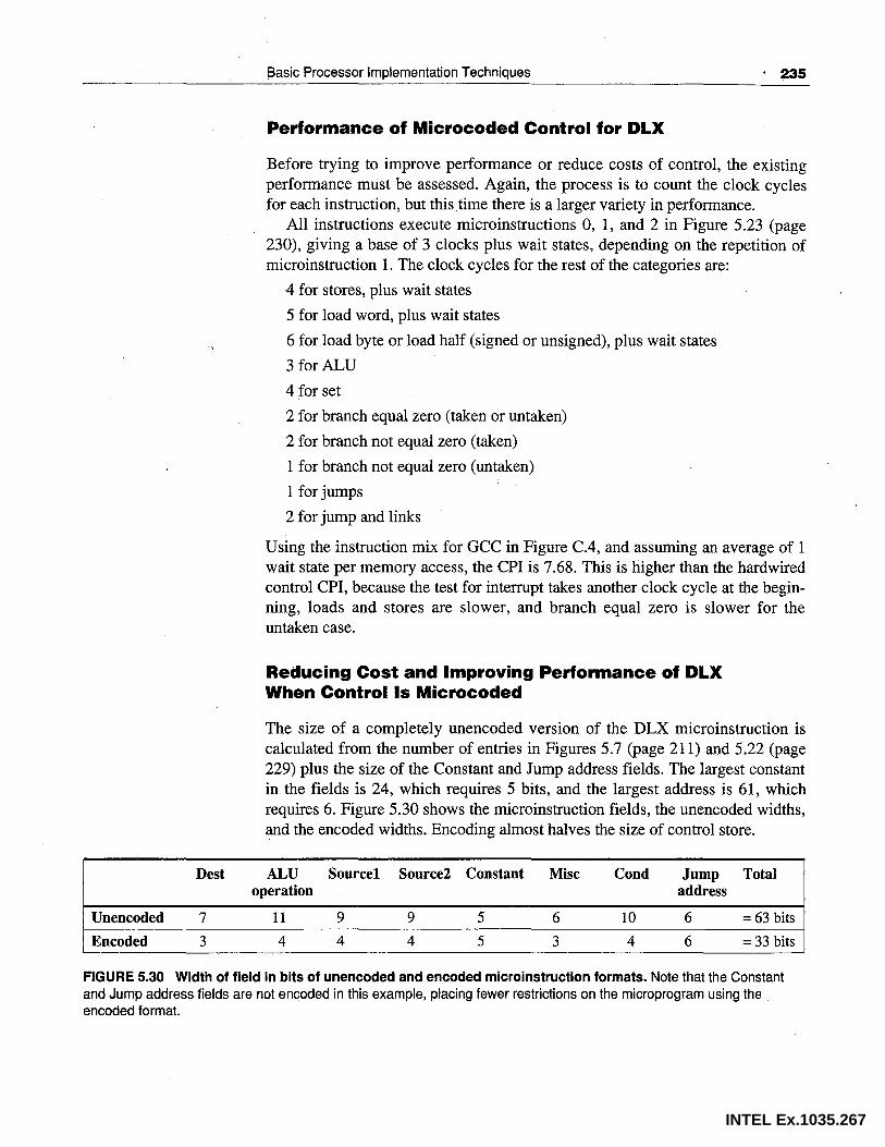
Dest
Unencoded 7
Encoded 3
Basic Processor Implementation Techniques . 235
Performance of Microcoded Control for DLX
Before trying to improve performance or reduce costs of control, the existing performance must be assessed. Again, the process is to count the clock cycles for each instruction, but this time there is a larger variety in performance.
All instructions execute microinstructions 0, 1, and 2 in Figure 5.23 (page 230), giving a base of 3 clocks plus wait states, depending on the repetition of microinstruction 1. The clock cycles for the rest of the categories are:
4 for stores, plus wait states
5 for load word, plus wait states
6 for load byte or load half (signed or unsigned), plus wait states
3 for ALU
4 for set
2 for branch equal zero (taken or untaken)
2 for branch not equal zero (taken)
1 for branch not equal zero (untaken)
1 for jumps
2 for jump and links
Using the instruction mix for GCC in Figure C.4, and assuming an average of 1 wait state per memory access, the CPI is 7.68. This is higher than the hardwired control CPI, because the test for interrupt takes another clock cycle at the beginning, loads and stores are slower, and branch equal zero is slower for the untaken case.
Reducing Cost and Improving Performance of DLX When Control Is Microcoded
The size of a completely unencoded version of the DLX microinstruction is calculated from the number of entries in Figures 5. 7 (page 211) and 5 .22 (page 229) phis the size of the Constant and Jump address fields. The largest constant in the fields is 24, which requires 5 bits, and the largest address is 61, which requires 6. Figure 5.30 shows the microinstruction fields, the unencoded widths, and the encoded widths. Encoding almost halves the size of control store.
ALU Sourcel Source2 Constant Misc Cond Jump Total operation address
11 9 9 5 6 10 6 = 63 bits
4 4 4 5 3 4 6 = 33 bits
FIGURE 5.30 Width of field in bits of unencoded and encoded microinstruction formats. Note that the Constant and Jump address fields are not encoded in this example, placing fewer restrictions on the microprogram using the encoded format.
INTEL Ex.1035.267

236
Example
Answer
5.7 Putting It All Together: Control for DLX
The microinstruction can be further shrunk by introducing multiple microinstruction formats and by combining independent fields.
Figure 5.31 shows an encoded version of the original DLX microinstruction format and the version with two formats: one for ALU operations and one for miscellaneous and branch operations. A bit is added to distinguish the two formats. The ALU/Jump (A/J) microinstruction performs the ALU operations specified in the microinstruction; the address of the next microinstruction is specified in the Jump address. For the Transfer/Misc/Branch (T/M/B) micro- ~
instruction, the ALU performs Pass S 1, while the Misc and Cond fields specify the rest of the operations. The primary change in interpretation of the fields in the new formats is that the ALU condition being tested in the T/M/B format refers to the ALU output from the prior A/J microinstruction since there is no ALU operation in T/M/B format. In both formats the Constant and Jump fields are combined into a single field under the assumption they are not used at the same time. (For the A/J format, the appearance of a constant in a source field results in fetching the following microinstruction.) The new formats shrink width from the original 33 bits to 22 bits, but the actual size savings depends on the number of extra microinstructions needed because of the reduced options.
What is the increase in number of microinstructions, compared to the single format, for the microcode in Figure 5.23 (page 230)?
3 4 4 4 5 3 4 6
ALU/Jump
3 4 4 4 6
Transfer/Misc/Branch
3 4 4 4 6
FIGURE 5.31 The original DLX microinstruction format at the top and the dual- ' format version below. Note that the Misc field is expanded from 3 to 4 bits in the T/M/B to make the two formats the same length.
Figure 5.32 shows the increase in the number of microinstructions over Figure 5.23 (page 230) because of the restrictions of each format. The five microinstructions in the original format expand to six in the new format. Microinstruction 2 is the only one that expands to two microinstructions for this example.
INTEL Ex.1035.268

Basic Processor Implementation Techniques 237
Loe Label Type. Dest ALU Sl S2 Misc Cond Const/ Comment Jump
0 If etch: M!f /B --- --- Interrupt? Intrpt Check interruJJt 1 !loop: M!f /B --- --- Instr Mem? !loop IR f-M[PC]; wait
Read for memory 2 A/J PC ADD PC Constant --- --- 4 Increment PC 3 M{f /B --- --- ABf- Decodel
RF
4 In trot: A/J IAR Pass Sl PC --- --- 5 Interrupt 5 A/J PC SUB Temp Temp --- --- If etch PC~O (t minus t=O) ..
& go fetch next instruction
FIGURE 5.32 Version of Figure 5.23 (page 230) using the dual-format microinstruction in Figure 5.31. Note that ALU/Jump microinstructions check the 81 and 82 fields for a constant specifier to see if the next address is sequential (as in microinstruction 2); otherwise they go to the Jump address (as in microinstructions 4 and 5). The microprogrammer changed the last microinstruction to generate a zero by subtracting a register from itself rather than through straightforward use of constant 0. Using the constant would have required an additional microinstruction since this format goes to the next sequential instruction if a constant is used. (See Figure 5.31.)
Loe Label Dest
50 Beq:
51 PC
Sometimes performance can be improved by finding faster sequences of microcode, but normally it requires changes to the hardware. The branch equal zero instruction takes one extra clock cycle when the branch is not taken with hardwired control, but two with microcoded control; while branch not equal zero has the same performance for hardwired and microcoded control. Why would the former differ in performance? Figure 5.29 shows that microinstruction 52 branches on zero to fetch the next microinstruction, which is correct for the branch on not equal zero macroinstruction. Microinstruction 50 also tests for zero for the branch on zero macroinstruction and branches to the microinstruction that loads the new PC. The not zero case is handled by the following microinstruction (51 ), which jumps to fetch the next instructionhence, one clock cycle for untaken branch on not equal zero and two for untaken branch on equal zero. One solution is simply to add "not zero" to the microcode branch conditions in Figure 5.22 (page 229) and change the branch on equal microcode to the version in Figure 5.33. Since there are only ten branch conditions, adding the eleventh would not require more than the four bits needed for an encoded version of that field.
ALU Sl S2 c Misc Cond Jump Comment label
SUB A Constant 0 notO? !fetch Branch =0 ADD PC imm16 Uncond If etch =0: taken
FIGURE 5.33 Branch not equal microcode from Figure 5.29 (page 234) rewritten by using a not zero condition in microinstruction 44.
INTEL Ex.1035.269

238
Example
Answer
Loe Label Dest
0 !fetch:
1 PC
2 Intrpt: IAR
3 PC
5.7 Putting It All Together: Control for DLX
This change drops the CPI from 7 .68 to 7 .63 for microcoded control, yet this is still higher than the CPI for hardwired control.
Let's improve microcoded control so that the CPI for GCC is closer to the original CPI under hardwired control.
The main performance culprit is the separate test for interrupts in Figure 5.23. By modifying the hardware, decodel can kill two birds with one stone: In addition to jumping to the appropriate microinstructions corresponding to the opcode, it also jumps to the interrupt microcode if an interrupt is pending. Figure 5.34 shows the revised microcode. This modification saves one clock cycle from each instruction, reducing the CPI to 6.63.
ALU Sl S2 c Misc Cond Jump Comment label
Instr Read Mem? If etch IR <::-M[PC]; wait for memory
ADD PC Constant 4 AB<::-RF Decode I Also go to interrupt if vendinR interrupt
SUB PC Constant 4 Interrupt: undo PC increment
Pass S2 Constant 0 Uncond If etch PC<::-0 & go fetch next instruction
FIGURE 5.34 Revised microcode that takes advantage of a change of the hardwar-e1o have decode1 go to microinstruction 2 if there is a pending interrupt. This microinstruction must reverse the increment of PC in the prior microinstruction so that the correct value is saved.
5.8 I Fallacies and Pitfalls ,
Pitfall: Microcode implementing a complex instruction may not be faster than macrocode.
At one time, microcode had the advantage of being fetched from a much faster memory than macrocode. Since caches came into use in 1968, microcode no longer has such a consistent edge in fetch time. Microcode does, however, still have the advantage of using internal temporary registers in the computation, which can be helpful on machines with few general-purpose registers. The disadvantage of micn:~code is that the algorithms must be selected before the machine is announced and can't be changed until the next model of the archi-
INTEL Ex.1035.270

Basic Processor Implementation Techniques 239
tecture; macrocode, · on the other hand, can utilize improvements in its algorithms at any time during the life of the machine.
The VAX Index instruction provides an example: The instruction checks to see if the index is between two bounds, one of which is usually zero. The VAX-11/780 microcode uses two compares and two branches to do this, while macrocode can perform the same check in one compare and one branch. The macrocode checks the· index against the upper limit using unsigned comparisons, rather than two's complement comparisons. This treats a negative index (less than zero and so failing the comparison) as if it were a very large
J number, thus exceeding the upper limit. (The algorithm can be used with nonzero lower bounds by first subtracting the lower bound from the index.) Replacing the index instruction by this VAX macrocode always improves performance on the V AX-11/780.
Fallacy: If there is space in control store, new instructions are free of cost.
Since the length of control store is usually a power of two, at times there may be unused control store available to expand the instruction set. The analogy here is that of building a house and discovering, near completion, that you have enough land and materials left to add a room. This room wouldn't be free, however, since there would be the costs of labor and maintenance for the life of the home. The temptation to add "free" instructions can only occur when the instruction set is not fixed, as is likely to be the case in the first model of a computer. Because instruction set compatibility is a long-term requirement, all future models of this machine will be forced to include these "free" instructions, even if space is later at a premium. This expansion also ignores the cost of a longer development time to test the added instructions, as well as the possibility of costs of repairing bugs in them after the hardware is shipped.
Fallacy: Usersfindwritable control store helpful.
Bugs in microcode persuaded designers of minicomputers and mainframes that it would be wiser to use RAM than ROM for control store. Doing so would enable microcode bugs to be repaired by shipping customers floppy disks rather than by having the field engineer pull boards and replace chips. Some customers and some manufacturers also decided that users should be allowed to write microcode; this opportunity became known as writable control store (WCS). Yet by the time WCS was offered, the world had changed to make WCS less attractive than originally envisioned:
• The tools for writing microcode were much poorer tha~ those for writing macrocode. (The authors and many others stepped into that breach to provide better microprogramming tools.)
• At a time when main memory was expanding, WCS was limited to 1-4KB microinstructions. (Few programming tasks are harder than forcing code into too small a memory.)
INTEL Ex.1035.271
240
5.9 I
5.8 Fallacies and Pitfalls
• Microcoded control became increasingly tailored to the native macroinstruction set, making microprogramming less useful for tasks other than that for which it was intended.
• With the advent of timesharing, programs might run for only milliseconds before switching to other tasks. This meant that WCS would have to be swapped if more than one program needed it, and reloading WCS could easily take longer than a few milliseconds.
• Timesharing also meant that programs had to be protected from each other. Because, at such a low level, microprograms can circumvent all protection barriers, microprograms written by users were notori~usly untrustworthy.
• The increasing demand for virtual memory meant that microprograms had to be restartable-any memory access could force the computation to be shelved.
• Finally, companies like DEC that offered WCS provided no customer support for those who wanted to write microcode.
Many customers ordered WCS, but few benefited from it. The death of WCS has been by a thousand small cuts, and WCS is not an option on current computers.
Concluding Remarks
In his first paper [1953] Wilkes identified advantages of microprogramming that still hold true today. One of these advantages is that microprogramming helps accommodate change. This can happen late in the development cycle, where simply changing some Os to ls in the control store can sometimes save redesigning hardware. A related advantage is that by emulating other instruction sets in microcode, software compatibility is simplified. Microprogramming also reduces the cost of adding more complex instructions to a standard microarchitecture to just the cost of a few more words of control store (although there is the pitfall that once an instruction set is created assuming microprogrammed control, it is difficult to ever build a machine without using it). This flexibility allows hardware construction to begin before the instruction set and microcode have been completely written, because specifying control -is just a matter of programming. Finally, microprogramming now has the further advantage of having a large set of tools that have been developed to help write, edit, assemble, and debug microcode.
The drawback of microcode has always been performance. This is because microprogramming is a slave to memory tecnnology: The clock cycle time is limited by the time to read microinstructions from control store. In the 1950s, microprogramming was impractical since virtually the only technology available for control store was the same one used for main memory. In the late 1960s and
INTEL Ex.1035.272

Basic Processor Implementation Techniques 241
early 1970s, semiconductor memory was available for control store, while main memory was constructed from core. The factor of ten in cycle time that differentiated the two technologies opened the door for microcode. The popularity of cache memory in the 1970s once again closed this gap, and machines were again built with the same technology for control store and memory.
For these reasons instruction sets invented since 1985 have not relied on . microcode. Though no one likes to predict the future-least of all in writing-it
is the authors' opinion that microprogramming is bound to memory technology. If in some future technology ROM becomes much faster than RAM, or if caches are no longer effective, microcode may regain its popularity.
5.1 0 I Historical Perspective and References
Interrupts go back to computer industry pioneers Eckert and Mauchly. Interrupts were first used to signal arithmetic overflow on the UNIVAC I and later to alert a UNIV AC 1103 to start online data collection for a wind tunnel (see Codd [1962]). After the success of the first commercial computer, the UNIVAC 1101 in 1953, the first commercial computer to have interrupts, the 1103, was brought out. Interrupts were first used for I/0 by AL. Leiner in the National Bureau of Standards DYSEAC [Smotherman 1989].
Maurice Wilkes learned computer design in a summer workshop from Eckert and Mauchly and then went on to build the first full-scale, operational, storedprogram computer-the EDSAC. From that experience he realized the difficulty of control. He thought of a more centralized control using a diode matrix and, after visiting the Whirlwind computer in the U.S., wrote:
I found that it did indeed have a centralized control based on the use of a matrix of diodes. It was, however, only capable of producing a fixed sequence of 8 pulses-a different sequence for each instruction, but nevertheless fixed as far as a particular instruction was concerned. It was not, I think, until I got back to Cambridge that I realized that the solution was to turn the control unit into a computer in miniature by adding a second matrix to determine the flow of control at the microlevel and by providing for conditional microinstructions. [Wilkes 1985, 178]
Wilkes [1953] was ahead of his time in recognizing that problem. Unfortunately, the solution was also ahead of its time: To provide control, microprogramming relies on fast memory that was not available in the 1950s. Thus, Wilkes's ideas remained primarily academic conjecture for a decade, although he did construct the EDSAC 2 using microprogrammed control in 1958 with ROM made from magnetic cores.
INTEL Ex.1035.273

242 5.10 Historical Perspective and References
IBM brought microprogramming into the spotlight in 1964 with the IBM 360 family. Before this event, IBM saw itself as many small businesses selling different machines with their own price and performance levels, but also with their own instruction sets. (Recall that little programming was done in high-level languages, so that programs written for one IBM machine would not run on another.) Gene Amdahl, one of the chief architects of the IBM 360, said that managers of each subsidiary agreed to the 360 family of computers only because they were convinced that microprogramming made it feasible-if you could take the same hardware and microprogram it with several different instruction sets, they reasoned, then you must also be able to take different hardware and microprogram them to run the same instruction set. To be sure of the viability of microprogramming, the IBM vice president of engineering even visited Wilkes surreptitiously and had a "theoretical" discussion of the pros and cons of microcode. IBM believed the idea was so important to their plans that they pushed the memory technology inside the company to make microprogramming feasible.
Stewart Tucker of IBM was saddled with the responsibility of porting software from the IBM 7090 to the new IBM 360. Thinking about the · possibilities of microcode, he suggested expanding the control store to include simulators, or interpreters, for older machines. Tucker [1967] coined the term emulation for this, meaning full simulation at the microprogrammed level. Occasionally, emulation on the 360 was actually faster than the original hardware. Emulation became so popular with customers in the early years of the 360 that it was sometimes hard to tell which instruction set ran more programs.
Once the giant of the industry began using microcode, the rest soon followed. A difficulty in adopting microcode was that the necessary memory technology was not widely available, but that was soon solved by semiconductor ROM and later RAM. The microprocessor industry followed the same history, with limited resources of the earliest chips forcing hardwired control. But as the resources increased, the advantages of simpler design and ease of change persuaded many to use microprogramming.
With the increasing popularity of microprogramming came more sophisticated instruction sets, including virtual memory. Microprogramming may well have aided the spread of virtual memory, since microcode made it easier to cope with the difficulties that arose from mapping addresses and restarting instructions. The IBM 370 model 138, for example, implemented virtual memory entirely in microcode without any hardware support.
Over the years, most microarchitectures became more and more dedicated to support the intended instruction set, so that reprogramming for a different instruction set failed to off er satisfactory performance. With the passage of time came much larger control stores, and it became possible to consider a machine as elaborate as the VAX. To offer a single chip VAX in 1984 DEC reduced the instructions interpreted by microcode by trapping some instructions and performing them in software: 20% of VAX instructions are responsible for 60% of the microcode, yet are only executed 0.2% of the time. Figure 5.35 shows the
INTEL Ex.1035.274

Basic Processor Implementation Techniques 243
reduction in control store by subsetting the instruction set. (The VAX is so tied to microcode that we venture to predict it will be impossible to build a fullinstruction-set VAX without microcode.) The microarchitecture of one of the simpler subsetted VAXes, the MicroVAX-I, is described in Levy and Eckhouse [1989].
Full instruction set Subset instruction set (VLSI VAX) (MicroVAX 32)
% instructions implemented 100% 80%
Size of control store (bits) 480K 64K
Number of chips in processor 9 2
% performance ofVAX-11/780 100% 90%
FIGURE 5.35 By trapping some VAX instructions and addressing modes, control store was reduced almost eight-fold. The second chip of the subset VAX is for floating point.
While this book was being written, a landmark legal precedent concerning microcode was set. The question under litigation in NEC v. Intel was whether microcode is like writing, and thereby deserves copyright protection (Intel), or whether it is like hardware, which can be patented but not copyrighted (NEC). The importance of this matter lies in the fact that while it is triviaL to get a copyright, getting a patent can take as long as a college education. A program can be copyrighted, so the question then follows: What is and isn't a program? Here is the legislated definition:
A 'computer program' is a set of statements or instructions to be used directly or indirectly in a computer in order to bring about a certain result.
After years of preparation and trial, a judge did declare that a microprogram was a program. The lawyers for the losing side then asked him to rescind his decision on grounds of partiality. They had discovered that through an investment club, the judge owned $80 of stock belonging to the client he ruled for. (The tempting sum really was only $80, highly frustrating to one of the authors who acted as an expert witness on the case!) The case was retried, and the new judge ruled that "microcode ... comes squarely within the definition of a 'computer program' ... " [Gray 1989, 4]. Of course, the fact that two judges in two different trials made the same decision doesn't mean that the matter is closed-there are still higher levels of appeal available.
INTEL Ex.1035.275

244 5.10 Historical Perspective and References
References
CLARK, D. W., P. J. BANNON, AND J.B. KELLER [1988]. "Measuring VAX 8800 performance with a histogram hardware monitor," Proc. 15th Annual Symposium on Computer Architecture (MayJune), Honolulu, Hawaii, 176-185.
CODD, E. F. [1962]. "Multiprogramming," in F.L. Alt and M. Rubinoff, Advances in Computers, vol. 3, Academic Press, New York, 82.
EMER, J. S. AND D. W. CLARK [1984]. "A characterization of processor performance in the VAX-11/780," Proc. 11th Symposium on Computer Architecture (June), Ann Arbor, Mich., 301-310.
GRAY, W. P. [1989]. Memorandum of Decision, No. C-84-20799-WPG, U.S. District Court for the Northern District of California (February 7, 1989).
LEVY, H. M. AND R.H. ECKHOUSE, JR. [1989]. Computer Programming and Architecture: The VAX, 2nd ed., Digital Press, Bedford, Mass. 358-372
MCKEVITT, J., ET AL. [1977]. 8086 Design Report, internal memorandum.
PATTERSON, D. A. [1983]. "Microprogramming," Scientific American 248:3 (March), 36-43.
REIGEL, E.W., U. FABER, AND D. A. FISCHER, [1972]. "The Interpreter-a microprogrammable building block system," Proc. AF1PS 1972 Spring Joint Computer Conj. 40, 705-723.
SMOTHERMAN, M. [1989]. "A sequencing-based taxonomy ofl/0 systems and review of historical machines," Computer Architecture News 17:5 (September), 5-15.
TUCKER, S. G. [1967]. "Microprogram control for the System/360," IBM Systems Journal 6:4, 222-241.
WILKES, M. V. [1953]. "The best way to design an automatic calculating machine," in Manchester University Computer Inaugural Conj., 1951, Ferranti, Ltd., London. (Not published until 1953.) Reprinted in "The Genesis of Microprogramming" in Annals of the History of Computing 8: 116.
WILKES, M. V. [1985]. Memoirs of a Computer Pioneer, The MIT Press, Cambridge, Mass.
WILKES, M. V. AND J.B. STRINGER [1953]. "Microprogramming and the design of the control circuits in an electronic digital computer," Proc. Cambridge Philosophical Society 49:230-238. Also reprinted in D. P. Siewiorek, C. G. Bell, and A. Newell, Computer Structures: Principles and Examples (1982), McGraw-Hill, New York, 158-163, and in "The Genesis of Microprogramming" in Annals of the History of Computing 8:116.
EXERCISES
If finite-state diagrams and microprogramming are review topics, you may want to skip over questions 5.5 through 5.14.
5.1 [15/10/15/15] <5.5> One technique that tries to get the best of both the worlds of vertical and horizontal microarchitectures is a two-level control store, as illustrated by Figure 5.36. It tries to combine small control-store size with wide instructions. To avoid confusion the bottom level uses the prefix nano-, yielding the terms "nanoinstruction," "nanocode," and so forth. This technique was used in the Motorola 68000, 68010, and 68020, but it was originated in the Burroughs D-machine [Reigel, Faber, and Fischer 1972]. The idea is that the first level has many vertical instructions that point to the few unique horizontal instructions in the second level. The Burroughs D-machine was a general-purpose computer offering writable control store. Its microinstructions were 16 bits wide, with 12 of those bits specifying a nanoaddress, and the nanoinstructions were 56 bits wide. One instruction set interpreter used 1124 microinstructions and 123 nanoinstructions.
INTEL Ex.1035.276
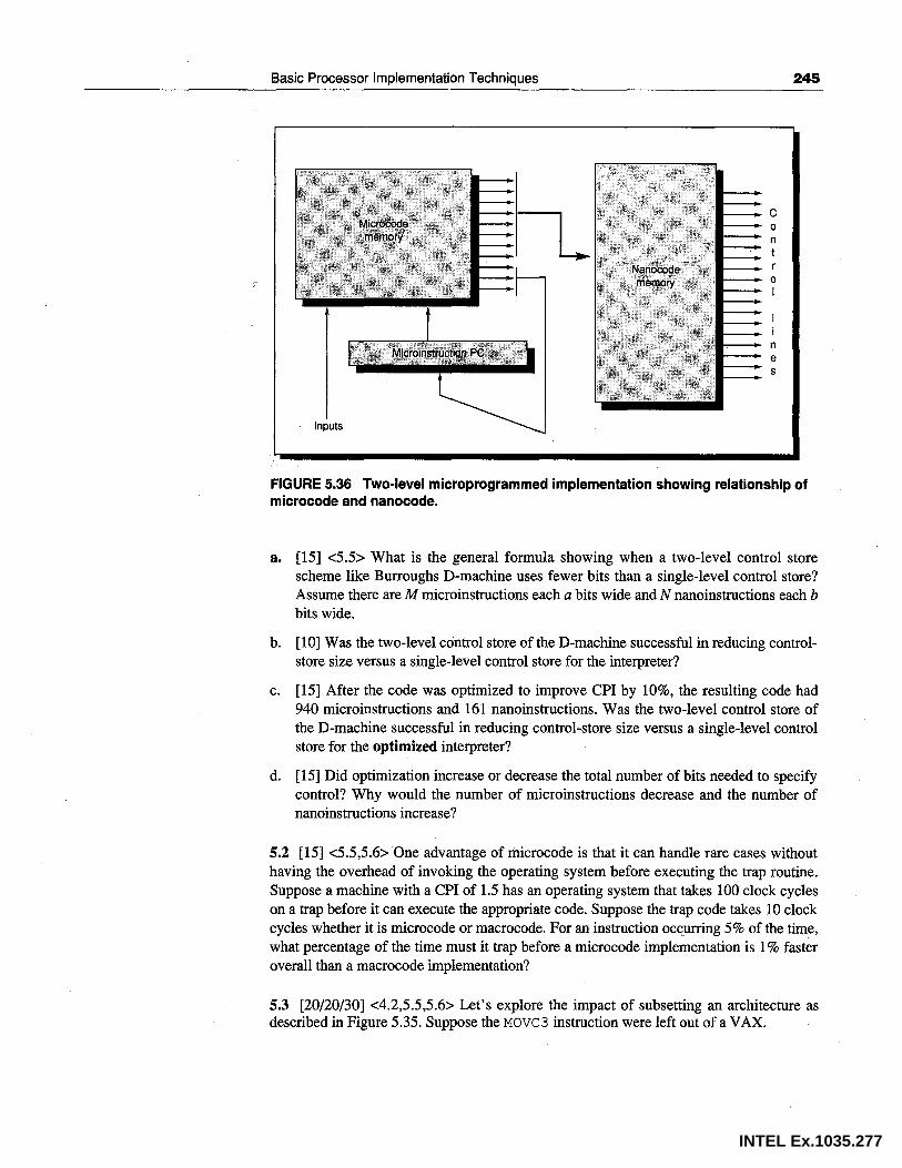
Basic Processor Implementation Techniques 245
FIGURE 5.36 Two-level microprogrammed implementation showing relationship of microcode and nanocode.
a. [15] <5.5> What is the general formula showing when a two-level control store scheme like Burroughs D-machine uses fewer bits than a single-level control store? Assume there are M microinstructions each a bits wide and N nanoinstructions each b bits wide.
b. [10] Was the two-level control store of the D-machine successful in reducing controlstore size versus a single-level control store for the interpreter?
c. [15] After the code was optimized to improve CPI by 10%, the resulting code had 940 microinstructions and 161 nanoinstructions. Was the two-level control store of the D-machine successful in reducing control-store size versus a single-level control store for the optimized interpreter?
d. [15] Did optimization increase or decrease the total number of bits needed to specify control? Why would the number of microinstructions decrease and the number of nanoinstructions increase?
5.2 [15] <5.5,5.6> One advantage of microcode is that it can handle rare cases without having the overhead of invoking the operating system before executing the trap routine. Suppose a machine with a CPI of 1.5 has an operating system that takes 100 clock cycles on a trap before it can execute the appropriate code. Suppose the trap code takes 10 clock cycles whether it is microcode or macrocode. For an instruction occurring 5% of the time, what percentage of the time must it trap before a microcode implementation is 1 % faster overall than a macrocode implementation?
5.3 [20/20/30] <4.2,5.5,5.6> Let's explore the impact of subsetting an architecture as described in Figure 5.35. Suppose the MOVC3 instruction were left out of a VAX.
INTEL Ex.1035.277

246 Exercises
a. [20] Write the VAX macrocode to replace MOVC3.
b. [20] Assume the operands are placed in registers RO, Rl, and R2 after a trap. Using the data for COBOLX in Figure C.1 in Appendix Con instruction usage (assuming ~)
all MOVC_ are MOVC3) and assuming the average MOVC3 moves 15 bytes, what would be the percentage change in instruction count if MOVC3 were not interpreted by microcode? (Ignore the cost of traps for this instruction.)
c. [30] If you have access to a VAX, time the speed of MOVC 3 versus a macrocode version of the routine from part a. Assuming that the trap overhead is 20 clock cycles, what is the impact on performance of trapping to software for MOVC 3?
5.4 [15] <5.6> Assume we have a machine with a clock cycle time of 10 ns and a base CPI of 5. Because of the possibilities of interrupts we must have extra registers containing copies of the values of the registers at the beginning of the instruction. These registers are usually called shadow registers. Assume that the average instruction has two register operands that must be restored on an interrupt. The interrupt rate is 100 interrupts per second, and the interrupt cost is 30 cycles plus the time to restore the shadowed registers, each of which takes 10 cycles. What is the effective CPI after accounting for interrupts? What is the performance lost from interrupts?
5.5-5. 7 Given the processor design and finite-state diagram for DLX as modified in the end of the hardwired-control portion of Section 5.7, explore the impact of performance of the following changes. In each case show the modified portion of the finite-state machine, describe the changes to the processor (if necessary), the change in the number of states, and calculate the change in CPI using the DLX instruction mix statistics in Figure C.4 for GCC. Show the reasons for the change.
5.5 [12] <5.7> Like the change to the ALU instructions in the second example in Section 5.7 and shown in Figures 5.20 and 5.21, remove the states that load Temp for the Set instructions in Figure 5.16 first by adding the "X" option and then by increasing the number of states.
5.6 [15] <5.7> Suppose that the memory interface was optimized so that it was not necessary to load MAR before a memory access, nor did the data have to be transferred in MDR for a read or write. Instead, any register on the S 1 bus could specify the address, any register on the S2 bus could supply the data on a write, and any register on the Dest bus could receive data on a read.
5.7 [22] <5.7> Most computers overlap the fetching of the next instruction with the execution of the current instruction. Propose a scheme that overlaps all instruction fetches except jumps, branches, and stores. You must reorganize the finite-state machine so that the instruction is already fetched, possibly even partially decoded.
5.8 [15] <5.7> The example in Section 5.7 on page 228 assumes everything but the shifter can scale to 9 ns. Alas, the memory system can rarely scale as easily as the CPU. Reperform the analysis in this example, but this time assume that average number of memory wait states is 2 at the 9-ns clock cycle versus 1 at 10 ns in addition to the slowdown for shifts.
INTEL Ex.1035.278

Basic Processor Implementation Techniques 247
5.9-5.14 These questions address use of the microcoded control of DLX as shown in Figures 5.23, 5.25, and 5.27-5.29. In each case show the modified portion of the microcode; describe the changes to the processor (if necessary), the microinstruction fields (if necessary), and the change in the number of microinstructions; and calculate the change in CPI using the DLX instruction-mix statistics in Appendix C for GCC. Show the reasons for the change.
5.9 [15] <5.7> Like the change to the ALU instructions in the second example in Section 5.7, remove the microinstructions that load Temp for the Set instructions in Figure 5.28 (page 233) first by adding the "X" option and then by increasing the number of microinstructions.
5.10 [25] <5.7> Continuing the example in Figure 5.32 (page 237), rewrite the microcode found in Figure 5.29 (page 234) using the dual-format microinstructions of Figure 5.31 (page 236). What is the relative frequency of each type of microinstruction? What is the savings in control-store size versus the original DLX format? What is the change in CPI?
5.11 [20] <3.4, 5.7> Load byte and Load half take a clock cycle longer than Load word because of the alignment of data (see Figure 3.10 on page 97 and Figure 5.25 on page 231 ). Propose a change that eliminates the extra clock for these instructions. How does this change affect the CPI of GCC? How does it affect the CPI of TeX?
5.12 [20] <5.6, 5.7> Change the microcode to perform the following interrupt tests: page fault, arithmetic overflow or underflow, misaligned memory accesses, and using undefined instructions. Make whatever changes are needed to the microarchitecture and microinstruction format. What is the change in size and performance to perform these tests?
5.13 [20] <5.7> The computer designer must be careful not to tailor her design too closely to a particular, single program. Reevaluate the performance impact of all the example performance improvements in Exercises 5.9 to 5.12 this time using the average instruction mix data in Figure C.4. How do the programs affect the evaluations?
5.14 [20] <5.6, 5.7> Starting with the microcode in Figures 5.27 (page 233) and 5.34 (page 238), revise the microcode so that the next macroinstruction is fetched as early as possible during the ALU instructions. Assume a "perfect" memory system, taking one clock cycle per memory reference. Although technically this improvement speeds up instructions that follow ALU instructions, the easiest way to account for higher performance is as faster ALU instructions. How much faster are the ALU instructions? How does it affect overall performance according to GCC statistics?
5.15 [30] <4,5.6> If you have access to a machine that uses one of the instruction sets in Chapter 4, determine the worst-case interrupt latency for that implementation of the architecture. Be sure you are measuring the raw machine latency and not the operating system overhead.
5.16 [30] <5.6> Computer architects have sometimes been forced to support instructions that were never published in the original instruction set manual. This situation arises
INTEL Ex.1035.279

248 Exercises
because some programs are created that inadvertently set unused instruction fields to values other than the architect expected, which raises havoc when the architect tries to use those values to extend the instruction set. IBM solved that problem in the System 370 by trapping on every possible undefined field. Try executing instructions with undefined fields on a computer to see what happens. Do your new instructions compute anything useful? If so, would you use these new instructions in programs?
5.17 [35] <5.4, 5.5, 5.7> Take the datapath in Figure 5.1 and build a simulator that can perform any of the operations needed to implement the DLX instruction set. Now implement the DLX instruction set using:
Microprogrammed control, and
Hardwired control.
For hardwired control see if you can find PLA minimization and state-assignment programs to reduce the cost of control. From these two designs, determine the performance of each implementation and the cost in terms of gates or in terms of silicon area.
5.18 [35] <2.2, 5.5, 5.7> The similarities between the microinstructions and the macroinstructions of DLX suggest that performance can be gained by writing a program that translates from DLX macrocode to DLX microcode. (This is the insight that inspired WCS.) Write such a program and benchmark it. What is the resulting expansion of code size?
5.19 [50] <2.2, 4.4, 5.10> Recent attempts have been made to run existing software on hardwired control machines by building hand-tuned simulators for popular machines. Write such a simulator for the 8086 instruction set. Run some existing IBM PC programs, and see how fast your simulator is relative to an 8-MHz 8086.
5.20 [Discussion] <4,5.5,5.10> Hypothesis: If the first implementation of an architecture uses microprogramming, it affects the instruction set architecture. Why might this be true? Looking at examples in Chapter 4 or elsewhere, give supporting or contradicting evidence from real machines. Which machines will always use microcode? Why? Which machines will never use microcode? Why? What control implementation do you think the architect had in mind when designing the instruction set architecture?
5.21 [Discussion] <5.5,5.10> Wilkes invented microprogramming in large to simplify construction of control. Since 1980 there has been an explosion of computer-aided design software whose goal is also to simplify construction of control. Hypothesis: The advances in computer-aided design software have rendered microprogramming unnecessary. Find evidence to support and refute the hypothesis.
5.22 [Discussion] <5.10> The DLX instructions and the DLX mi<;:roinstructions have many similarities. What would make it difficult for a compiler to produce DLX microcode rather than macrocode? What changes to the microarchitecture would make the DLX microcode more useful for this application?
INTEL Ex.1035.280

INTEL Ex.1035.281

It is quite a three-pipe problem.
Sir Arthur Conan Doyle, The Adventures of Sherlock Holmes
6.1 What Is Pipelining? 251
6.2 The Basic Pipeline for DLX 252
6.3 Making the Pipeline Work 255
6.4 The Major Hurdle of Pipelining-Pipeline Hazards 257
6.5 What·Makes Pipelining Hard to Implement 278
6.6 Extending the DLX Pipeline to Handle Multicycle Operations 284
6.7 Advanced Pipelining-Dynamic Scheduling in Pipelines 290
6.8 Advanced Pipelining-Taking Advantage of More Instruction-Level Parallelism 314
6.9 Putting It All Together: A Pipelined VAX 328
6.10 Fallacies and Pitfalls 334
6.11 Concluding Remarks 337
6.12 Historical Perspective and References 338
Exercises 343
INTEL Ex.1035.282

6.1
Pipelining
What Is Pipelining?
Pipelining is an implementation technique whereby multiple instructions are overlapped in execution. Today, pipelining is the key implementation technique used to make fast CPUs.
A pipeline is like an assembly line: Each step in the pipeline completes a part of the instruction. As in a car assembly line, the work to be done in an instruction is broken into smaller pieces, each of which takes a fraction of the time needed to complete the entire instruction. Each of these steps is called a pipe stage or a pipe segment. The stages are connected one to the next to form a pipe-instructions enter at one end, are processed through the stages, and exit at the other end.
The throughput of the pipeline is determined by how often an instruction exits the pipeline. Because the pipe stages are hooked together, all the stages must be ready to proceed at the same time. The time required between moving an instruction one step down the pipeline is a machine cycle. The length of a machine cycle is determined by the time required for the slowest pipe stage (because all stages proceed at the same time). Often the machine cycle is one clock cycle (sometimes it is two, or rarely more), though the clock may have multiple phases.
INTEL Ex.1035.283

252 6.1 What Is Pipelining?
The pipeline designer's goal is to balance the length of the pipeline stages. If the stages are perfectly balanced, then the time per instruction on the pipelined machine-assuming ideal conditions (i.e., no stalls)-is equal to
Time per instruction on nonpipelined machine Number of pipe stages
Under these conditions, the speedup from pipelining equals the number of pipe stages. Usually, however, the stages will not be perfectly balanced; furthermore, pipelining does involve some overhead. Thus, the time per instruction on the pipelined machine will not have its minimum possible value, though it can be close (say within 10% ).
Pipelining yields a reduction in the average execution time per instruction. This reduction can be obtained by decreasing the clock cycle time of the pipelined machine or by decreasing the number of clock cycles per instruction, or by both. Typically, the biggest impact is in the number of clock cycles per instruction, though the clock cycle is often shorter in a pipelined machine (especially in pipelined supercomputers). In the advanced pipelining sections of this chapter we will see how deep pipelines can be used to both decrease the clock cycle and maintain a low CPI.
Pipelining is an implementation technique that exploits parallelism among the instructions in a sequential instruction stream. It has the substantial advantage that, unlike some speedup techniques (see Chapters 7 and 10), it is not visible to the programmer. In this chapter we will first cover the concept of pipelining using DLX and a simplified version of its pipeline. We will then look at the problems pipelining introduces and the performance attainable under typical situations. Later in the chapter we will examine advanced techniques that can be used to overcome the difficulties that are encountered in pipelined machines and that may lower the performance attainable from pipelining.
We use DLX largely because its simplicity makes it easy to demonstrate the principles of pipelining. The same, principles apply to more complex instruction sets, though the corresponding pipelines are more complex. We will see an example of such a pipeline in the Putting It All Together section.
6.2 j The Basic Pipeline for DLX
Remember that in Chapter 5 (Section 5.3) we discussed how DLX could be implemented with five basic execution steps:
1. IF-instruction fetch
2. ID-instruction decode and register fetch
3. EX--execution and effective address calculation
4. MEM-memory access
5. WB-write back
INTEL Ex.1035.284

Pipelining 253
Instruction Clock number number 1 2 3 4 . s 6 7 8 9
Instruction i IF ID EX MEM WB Instruction i+ 1 IF ID EX MEM WB Instruction i+2 IF ID EX MEM WB Instruction i+ 3 IF ID EX MEM WB Instruction i+4 IF ID EX MEM WB
FIGURE 6.1 Simple DLX pipeline. On each clock cycle another instruction is fetched and begins its five-step execution. If an instruction is started every clock cycle, the performance will be five times that of a machine that is not pipelined.
Example
Answer
We can pipeline DLX by simply fetching a new instruction on each clock cycle. Each of the steps above becomes a pipe stage-a step in the pipelineresulting in the execution pattern shown in Figure 6.1. While each instruction still takes five clock cycles, during each clock cycle the hardware is executing some part of five different instructions.
Pipelining increases the CPU instruction throughput-the number of instructions completed per unit of time-but it does not reduce the execution time of an individual instruction. In fact, it usually slightly increases the execution time of each instruction due to overhead in the control of the pipeline. The increase in instruction throughput means that a program runs faster and has lower total execution time, even though no single instruction runs faster!
The fact that the execution time of each instruction remains unchanged puts limits on the practical depth of a pipeline, as we will see in the next section. Other design considerations limit the clock rate that can be attained by deeper pipelining. The most important consideration is the combined effect of latch delay and clock skew. Latches are required between pipe stages, adding setup time plus the delay through those latches to each clock period. Clock skew also contributes to the lower limit on the clock cycle. Once the clock cycle is as small as the sum of the clock skew and latch overhead, no further pipelining is useful.
Consider a nonpipelined machine with five execution steps of lengths 50 ns, 50 ns, 60 ns, 50 ns, and 50 ns. Suppose that due to clock skew and setup, pipelining the machine adds 5 ns of overhead to each execution stage. Ignoring any latency impact, how much speedup in the instruction execution rate will we gain from a pipeline?
Figure 6.2 shows the execution pattern on the nonpipelined machine and on the pipelined machine. ,
The average instruction execution time on the nonpipelined machine is
Average instruction execution time= 50+50+60+50+50 ns = 260 ns
INTEL Ex.1035.285

254 6.2 The Basic Pipeline for DLX
I 260 I 260 .1 260 I
I 50 I 50 I 60 I 50 I 50 I 50 I 50 I 60 I 50 I 50 I 50 I 50 I 60 I 50 I 50 I Instruction 1 Instruction 2 Instruction 3
Nonpipelined execution
I 65 I 65 I 65 I 65 I 65 I
Instruction 1 60 60 60 60 60 I - I 60 60 60 60 60 Instruction 2
-Instruction 3 60 60 60 60 60
5 5 5 5 5
Pipelined execution
FIGURE 6.2 The execution pattern for three instructions shown for both the nonpipelined and pipelined versions. In the nonpipelined version, the three instructions are. executed sequentially. In the pipelined version, the shaded areas represent the overhead of 5 ns per pipestage. The length of the pipestages must all be the same: 60 ns plus the 5-ns overhead. The latency of an instruction increases from 260 ns in the nonpipelined machine to 325 ns in the pipelined machine.
In the pipelined implementation, the clock must run at the speed of the slowest stage plus overhead, which will be 60 + 5 or. 65 ns; this is the average instruction execution time. Thus, the speedup from pipelining is
_ Average instruction time without pipeline Speedup - Average instruction time with pipeline
260 4 . = 65
=. times
The 5-ns overhead essentially establishes a limit on the effectiveness of pipelining. If the overhead is not affected by changes in the clock cycle, Amdahl's Law tells us that the overhead limits the speedup.
Because the latches in a pipelined ·design can have a significant impact on the clock speed, designers have looked for latches that permit the highest possible clock rate. The Earle latch (invented by J. G. Earle [1965]) has three properties that maj<:e it especially useful in pipelined machines. First, it is relatively insensitive to clock skew. Second, the delay through the latch is always a constant two-gate delay, avoiding the introduction of skew in the data passing through the latch. Finally, two levels of logic can be done in the latch without increasing the latch delay time. This means that two levels of logic in the pipeline can be overlapped with the latch, so the majority of the overhead from the latch can be
INTEL Ex.1035.286
Pipelining 255
hidden. We will not be analyzing the pipeline designs in this chapter at this level of detaiL The interested reader should see Kunkel and Smith [1986].
The next two sections will add refinements and address some problems that can occur in this pipeline. In this discussion (up to the last segment of Section 6.5) we will focus on the pipeline for the integer portion of DLX. The complications that arise in the floating-point pipeline will be treated in Section 6.6.
6.3 I Making the Pipeline Work
Your instinct is right if you find it hard to believe that pipelining is as simple as this, because it's not. In this and the following three sections, we will make our DLX pipeline "real" by dealing with problems that pipelining introduces.
To begin with, we have to determine what happens on every clock cycle of the machine and make sure that overlapping instructions doesn't overcommit resources. For example, a single ALU cannot be asked to compute an effective address and perform a subtract operation at the same time. As we will see, the simplicity of the DLX instruction set makes resource evaluation relatively easy.
The operations that occur during instruction execution, which were discussed in Section 5.3 of Chapter 5, are modified to execute in a pipeline as shown in Figure 6.3. The figure lists the major functional units in our DLX implementation, the pipe stages, and what has to happen in each stage of the pipeline. The vertical axis is labeled with the pipeline stages, while the horizontal axis shows major resources. Each intersection shows what happens for that resource in that stage. In Figure 6.4 we will show similar information using the instruction type as the horizontal axis. The combination of instructions that may be in the pipeline at any one time is arbitrary. Thus, the combined needs of all instruction typys at any pipe stage determine what resources are needed at that stage.
Every pipe stage is active on every clock cycle. This requires all operations in a pipe stage to complete in one clock and any combination of operations to be able to occur at once. Here are the most important implications for the data path, as specified in Chapter 5:
1. The PC must be incremented on each clock. This must be done in IF rather than ID. This will require an additional incrementer, since the ALU is already busy on every cycle and cannot be used to increment the PC.
2. A new instruction must be fetched on every clock-this is also done in IF.
3. A new data word is needed on every clock cycle-this is done in MEM.
4. There must be a separate MDR for loads (LMDR) and stores (SMDR), since when they are back-to-back, they overlap in time.
5. Three additional latches are needed to hold values that are needed later in the pipeline, but· may be modified by a subsequent instruction. The values latched are the instruction, the ALU output, and the next PC.
INTEL Ex.1035.287

256 6.3 Making the Pipeline Work
PC unit Memory Data path Stage
IF PCf- PC+4; IRf-Mem[PC];
ID PClf- PC IRlf-IR Af- Rsl; Bf- Rs2;
EX 16 DMARf-A + (IRl16) ##IR116 .. 31; SMDRf-B; or ALUoutputf- A op (B or
16 (IRl16) ##IRl16 .. 31);
or ALUoutputf-PCl + 16
(IRl16) ##IRl16 .. 31i
condf- (A op 0) ;
MEM if (cond) LMDRf- Mem [DMAR] ALUoutputlf- ALUoutput PCf-ALUoutput or
Mem [ DMAR l f-SMDR
WB Rdf- ALUoutputl or LMDR
FIGURE 6.3 The table shows the major functional units and what may happen in every pipe stage in each unit. In several of the stages not all of the actions listed can occur, because they apply under different assumptions about the instruction. For example, there are three operations within the ALU during the EX stage. The first occurs only on a load or store; the second on ALU operations (with the input being B or the lower 16 bits of the IR, according to whether the instruction is register-register or register-immediate); the third operation occurs only on branches. For simplicity, we have shown the branch case only-jumps will add a 26-bit offset to the PC. The variables ALUouputl, PCl, and IRl save values for use in later stages of the pipeline. Designing the memory system to support a data load or l?tore on every clock cycle is challenging; see Chapter 8 for an in-depth discussion. This type of table and that in Figure 6.4 are loosely based on Davidson's [1971] pipeline reservation tables.
Stage ALU instruction Load or store instruction Branch instruction
IF IRf-Mem [PC l ; IRf-Mem [PC l ; IRf-Mem [PC] ; PCf-PC+4; PCf-PC+4; PCf-PC+4;
ID Af-Rsl; Bf-Rs2; PClf-PC Af-Rsl; Bf-Rs2; PClf-PC Af-Rsl; Bf-Rs2; PClf-PC IRlf-IR IRlf-IR IRlf-IR
EX ALUoutputf-A op B; DMARf-A+ ALUoutputf-PCl + or ( (IRl16) 16 ##IR116 .. 31); ( ( IR116) 16 # #IR116 .. 31) ; ~LUoutputf-A op SMDRf- B; condf- (A op 0) ;
( ( IRl16) 16 ##IR116 .. 31) ;
MEM ALUoutputlf- ALUoutput LMDRf-Mem [DMAR] ; or if (cond) PCf-ALUoutput; -
Mem [DMA:R] f-SMDR;
WB Rdf-ALUoutputl; Rdf-LMDR;
FIGURE 6.4 Events on every pipe stage of the DLX pipeline. Because the instruction is not yet decoded, the first two pipe stages are always identical. Note that it was critical to be able to fetch the registers before decoding the instruction; otherwise another pipeline stage would be required. Due to the fixed instruction format, both register fields are always decoded and the registers accessed (though they are sometimes not needed); the PC and immediate fields can be sent to · the ALU as well. At the beginning of the ALU operation the correct inputs are multiplexed in, based on the opcode. With this organization all instruction-dependent operations occur in the EX stage or later. As in Figure 6.3, we include the case for branches, but not jumps, which will have a 26-bit offset rather than a 16-bit offset. Jumps are essentially like branches.
INTEL Ex.1035.288

Pipelining 257
Probably the biggest impact of pipelining on the machine resources is in the memory system. Although the memory-access time has not changed, the peak memory bandwidth must be increased by five times over the nonpipelined machine because two memory accesses are required on every clock in the pipelined machine versus two accesses every five clock cycles in a nonpipelined machine with the same number of steps per instru£tion. To provide two memory accesses every clock, most machines will use separate instruction and data caches (see Chapter 8, Section 8.3).
During the EX stage, the ALU can be used for three different functions: an effective data-address calculation, a branch-address calculation, or an ALU instruction. Fortunately, the DLX instructions are simple; an instruction in EX does at most one of these, so no conflict arises.
The pipeline we now have for DLX would function just fine if every instruction were independent of every other instruction in the pipeline. In reality, instructions in the pipeline can be dependent on one another; this is the topic of the next section.
6.4 I The Major Hurdle of PipeliningPipeline Hazards
There are situations, called hazards, that prevent the next instruction in the instruction stream from executing during its designated clock cycle. Hazards reduce the performance from the ideal speedup gained by pipelining. There are three classes of hazards:
1. Structural hazards arise from resource conflicts when the hardware cannot support all possible combinations of instructions in simultaneous overlapped execution.
2. Data hazards arise when an instruction depends on the results of a previous instruction in a way that is exposed by the overlapping of instructions in the pipeline.
3. Control hazards arise from the pipelining of branches and other instructions that change the PC.
Hazards in pipelines can make it necessary to stall the pipeline. The major difference between stalls in a pipelined machine and stalls in a nonpipelined machine (such as those we saw in DLX in Chapter 5) occurs because there are multiple instructions under execution at once. A stall in a pipelined machine often requires that some instructions be allowed to proceed, while others are delayed. Typically, when an instruction is stalled, all instructions later in the pipeline than the stalled instruction are also stalled. Instructions earlier than the stalled instruction can continue, but no new instructions are fetched during the stall. We will see several examples of how stalls operate in this section-don't worry, they aren't as complex as they might sound!
INTEL Ex.1035.289

258 6.4 The Major Hurdle of Pipelining-Pipeline Hazards
A stall causes the pipeline performance to degrade from the ideal performance. Let's look at a simple equation for finding the actual speedup from pipelining, starting with the formula from the previous section.
_ Average instruction time without pipeline Pipeline speedup
- Average instruction time with pipeline
_ CPI without pipelining * Clock cycle without pipelining - CPI with pipelining * Clock cycle with pipelining
= Clock cycle without pipelining * CPI without pipelining Clock cycle with pipelining CPI with pipelining
Remember that pipelining can be thought of a~ decreasing the CPI or the clock cycle time; let's treat it as decreasing the CPI. The ideal CPI on a pipelined machine is usually
Ideal CPI = CPI "".ith~ut pipelining P1pelme depth
Rearranging this and substituting into the speedup equation yields:
S d _ Clock cycle without pipelining * Ideal CPI * Pipeline depth pee up - Clock cycle with pipelining CPI with pipelining
If we confine ourselves to pipeline stalls,
CPI with pipelining = Ideal CPI + Pipeline stall clock cycles per instruction
We can substitute and obtain:
S d _ Clock cycle without pipelining * Ideal CPI * Pipeline depth pee up - Clock cycle with pipelining Ideal CPI + Pipeline stall cycles
While this gives a general formula for pipeline speedup (ignoring stalls other than from the pipeline), in most instances a simpler equation can be used. Often, we choose to ignore the potential increase in the clock cycle due to pipelining overhead. This makes the clock rates equal and allows us to drop the first term. A simpler formula can now be used:
p· r d Ideal CPI * Pipeline depth ipe me spee up = Ideal CPI + Pipeline stall cycles
While we will use this simpler form for evaluating the DLX pipeline, a designer must be careful not to discount the potential impact on clock rate in evaluating pipelining strategies.
Structural Hazards
When a machine is pipelined, the overlapped execution of instructions requires pipelining of functional units and duplication of resources to allow all possible combinations of instructions in the pipeline. If some combination of instructions
INTEL Ex.1035.290

. <'
Instruction
Load instruction
Instruction i+ 1
Instruction i+2
Instruction i+ 3
Instruction i+4
1
Pipelining 259
cannot be accommodated due to resource conflicts, the machine is said to have a structural hazard. The most common instances of structural hazards arise when some functional unit is not fully pipelined. Then a sequence of instructions that all use that functional unit cannot be sequentially initiated in the pipeline. Another common way that structural hazards appear is when some resource has not been duplicated enough to allow all combinations of instructions in the pipeline to execute. For example, a machine may have only one register-file write port, but under certain circumstances, the pipeline might want to perform two writes in a clock cycle. This will generate a structural hazard. When a sequence of instructions encounters this hazard, the pipeline will stall one of the instructions until the required unit is available.
Many pipelined machines share a single memory pipeline for data and instructions. As a result, when an instruction contains a data-memory reference, the pipeline must stall for one clock cycle; the machine cannot fetch the next instruction because the data reference is using the memory port. Figure 6.5 shows what a one-memory-port pipeline looks like when it stalls during a load . We will see another type of stall when we talk about data hazards.
Clock cycle number 2 3 4 5 6 7 8 9
IF ID EX MEM WB
IF ID EX MEM WB
IF ID EX MEM WB
stall IF ID EX MEM WB
IF ID EX MEM
FIGURE 6.5 A pipeline stalled for a structural hazard-a load with one memory port. With only one memory port, the pipeline cannot initiate a data fetch and instruction fetch in the same cycle. A load instruction effectively steals an instruction-fetch cycle, causing the pipeline to stall-no instruction is initiated on clock cycle 4 (which normally would be instruction i+3). Because the instruction being fetched is stalled, all other instructions in the pipeline can proceed normally. The stall cycle will continue to pass through the pipeline.
Example
Answer
Suppose that data references constitute 30% of the mix and that the ideal CPI of the pipelined machine, ignoring the structural hazard, is 1.2. Disregarding any other performance losses, how much faster is the ideal machine without the memory structural hazard, versus the machine with the hazard?
The ideal machine will be faster by the ratio of the speedup of the ideal machine over the real machine. Since the clock rates are unaffected, we can use the following for speedup:
P.
1. d Ideal CPI * Pipeline depth
1pe me spee up = . . Ideal CPI + P1pelme stall cycles
INTEL Ex.1035.291

260
Example
Answer
6.4 The Major Hurdle of Pipelining-Pipeline Hazards
S. h 'd 1 h' h -all · d . . 1 1.2*Pipeline depth mce t e 1 ea mac me as no st s, its spee up 1s s1mp y 1.2
.
Th d f h al h. . 1.2*Pipeline depth_ l.2*Pipeline depth
e spee up o t ere mac me 1s 1.2 + 0.3*l - 1.5
(l.2*Pipeline depth)
SpeedUPideal = 1.2 = 1.5 = 1 25 SpeedUPreal (l.2*Pipeline depth) 1.2 ·
1.5
Thus, the machine without the structural hazard is 25% faster.
If all other factors are equal, a machine without structural hazards will always have a lower CPI. Why, then, would a designer allow structural hazards? There are two reasons: to reduce cost and to reduce the latency of the unit. Pipelining all the functional units may be too costly. Machines that support one-clock-cycle memory references require twice as much total memory bandwidth and often have higher bandwidth at the pins. Likewise, fully pipelining a floating-point multiplier consumes lots of gates. If the structural hazard would not occur often, it may not be worth the cost to avoid it. It is also usually possible to design a nonpipelined unit, or one that isn't fully pipelined, with a shorter total delay than a fully pipelined unit. For example, both the CDC 7600 and the MIPS R2010 floating-point unit choose shorter latency (fewer clocks per operation) versus full pipelining. As we will see shortly, reducing latency has other performance benefits and can frequently overcome the disadvantage of the structural hazard.
Many recent machines do not have fully pipelined floating-point units. For example, suppose we had an implementation of DLX with a 5-clock-cycle latency for floating-point multiply, but no pipelining. Will this structural hazard have a large or small performance impact on Spice running on DLX? For sim- _ plicity, assume that the floating-point multiplies are uniformly distributed.
The data in Figure C.4 show that floating-point multiply has a frequency of 6% in Spice. Our proposed pipeline can handle up to a 20% frequency of floatingpoint multiplies-one every five clock cycles. This means that the performance benefit of fully pipelining the floating-point multiply is likely to be low, as long as the floating-point multiplies are not clustered but are distributed uniformly. If they were clustered, the impact could be much larger.
Data Hazards
A major effect of pipelining is to change the relative timing of instructions by ~:>Verlapping their execution. This introduces data and control hazards. Data
INTEL Ex.1035.292

Instruction
ADD instruction
SUB instruction
Pipelining 261
hazards occur when the order of access to operands is changed by the pipeline versus the normal order encountered by sequentially executing instructions. Consider the pipelined execution of these instructions:
ADD Rl,R2,R3 SUB R4,Rl,R5
The SUB instruction has a source, R 1, that is the destination of the ADD instruction. As shown in Figure 6.6, the ADD instruction writes the value of Rl in the WB pipe stage, but the SUB instruction reads the value during its ID stage. This problem is called a data hazard. Unless precautions are taken to prevent it, the SUB instruction will read the wrong value and try to use it. In fact, the value
· used by the SUB instruction is not even deterministic: Though we might think it logical to assume that SUB would always use the value of Rl that was assigned by an instruction prior to ADD, this is not always the case. If an interrupt should occur between the ADD and SUB instructions, the WB stage of the ADD will complete, and the value of Rl at that point will be the result of the ADD. This unpredictable behavior is obviously unacceptable.
Clock cycle 1 2 3 4 5 6
IF ID EX MEM WB--data written here
IF ID-data read here EX MEM WB
FIGURE 6.6 The ADD instruction writes a register that is a source operand for the SUB instruction. But the ADD
doesn't finish writing the data into the register file until three clock cycles after SUB begins reading it!
The problem posed in this example can be solved with a simple hardware technique calledforwarding (also called bypassing and sometimes short-circuiting). This technique works as follows: The ALU result is always fed back to the ALU input latches. If the forwarding hardware detects that the previous ALU operation has written the register corresponding to a source for the current ALU operation, control logic selects the forwarded result as the ALU input rather than the value read from the register file. Notice that with forwarding, if the SUB is stalled, the ADD will be completed, and the bypass will not be activated, causing the value from the register to be used. This is also true for the case of an interrupt between the two instructions.
In our DLX pipeline, we must pass results to not only the instruction that immediately follows, but also to the instruction after that. ay the third instruction down the line, the ID and WB stages overlap; however, as the write is not finished until the end of WB, we must continue to forward the result. Figure·6.7 shows a set of instructions in the pipeline and the forwarding operations that can occur.
INTEL Ex.1035.293

262 6.4 The Major Hurdle of Pipelining-Pipeline Hazards
ADD Rl,R2,R3 IF ID EX MEM WB
,\
SUB R4,Rl,R5 IF ID ~ MEM WB
' )..
AND R6,Rl,R7 IF ID ·~ MEM WB
\
OR R8,Rl,R9 IF ID- EX MEM WB
XOR RlO, Rl, Rll
FIGURE 6.7 A set of instructions in the pipeline that need to forward results. The ADD instruction sets R1, and the next four instructions use it. The value of R1 must be bypassed to the SUB, AND, and OR instructions. By the time the' XOR instruction goes to read R1 in the ID phase, the ADD instruction has completed WB, and the value is available.
Rl,R2,R3 IF ID
ADD EX MEM WB
R w
SUB R4,Rl,R5 IF ID EX MEM WB
R w
AND R6,Rl,R7 IF ID EX MEM WB
R w
OR R8,Rl,R9 IF ID EX MEM WB
R w
RlO,Rl,Rll IF ID
XOR EX MEM WB
R w
FIGURE 6.8 The same instruction sequence as shown in Figure 6.7, with register reads and writes occurring in opposite halves of the ID and WB stages. The SUB and AND instructions will still require the value of R1 to be bypassed to them, and this will happen as they enter their EX stage. However, by the time of the OR instruction, which also uses R1, the write of R1 has completed, and no forwarding is required. The XOR depends on the ADD, but the value of R1 from the ADD is always written back the cycle before XOR
reaches its ID stage and reads it.
INTEL Ex.1035.294

Pipelining 263
It is desirable to cut down the number of instructions that must be bypassed, since each level requires special hardware. Remembering that the register file is accessed twice in a clock cycle, it is possible to do the register writes in the first half of WB and the reads in the second half of ID. This eliminates the need to bypass to a third instruction, as shown in Figure 6.8.
Each level of bypass requires a latch and a pair of comparators to examine whether the adjacent instructions share a destination and a source. Figure 6.9 shows the structure of the ALU and its bypass unit as well as what values are in
0 the bypass registers for the instruction sequence in Figure 6. 7. Two ALU result buffers are needed to hold ALU results to be stored into the destination register in the next two WB stages. For ALU operations, the result is always forwarded -when the instruction using the result as a source enters its EX stage. (The instruction that computed the value to be forwarded may be in its MEM or WB stages.) The results in the buffers can be inputs into either port on the ALU, via a pair of multiplexers. Multiplexer control can be done by either the control unit
. ' (which must then track the destinations and sources of all operations in the pipeline) or locally by logic associated with the bypass (in which case the bypass buffers will contain tags giving the register numbers the values are destined for). In either event, the logic must test if either of the two previous instructions wrote a register that is the input to the current instruction. If so, then the multiplexer select is set to choose from the appropriate result register rather than from the bus. Because the ALU operates in a single pipeline stage, there is no need for a pipeline stall with any combination of ALU instructions once the bypasses have been implemented.
Result write bus
Register file
Bypass paths
R4 ----m==:...:::i-ALU result buffers
R1
FIGURE 6.9 The ALU with its bypass unit. The contents of the buffer are shown at the point where the AND instruction of the code sequence in Figure 6.8 is about to begin the EX stage. The ADD instruction that computed R1 (in the second buffer) is in its WB stage, and the left input multiplexer is set to pass the just-computed value of R1 (not the value read from the register file) as the first operand to the AND instruction. The result of the subtract, R4, is in the first buffer. These buffers correspond to the variables ALUoutput and ALUoutputl in Figures 6.3 and 6.4.
INTEL Ex.1035.295

264 6.4 The Major Hurdle of Pipelining-Pipeline Hazards
A hazard is created whenever there is a dependence between instructions, and they are close enough that the overlap caused by pipelining would change the order of access to an operand. Our example hazards have all been with register operands, but it is also possible for a pair of instructions to create a dependence by writing and reading the same memory location. In our DLX pipeline, however, memory references are always kept in order, preventing this type of hazard from arising. Cache misses could cause the memory references to get out of order if we allowed the processor to continue working on later instructions while an earlier instruction that missed the cache was accessing memory. For DLX's pipeline we just stall the entire pipeline, effectively making the instruction that contained the miss run for multiple clock cycles. In an advanced section of this chapter, Section 6. 7, we will discuss machines that allow loads and stores to be executed in an order different from that in the program. All the data hazards discussed in this section, however, involve registers within the CPU.
Forwarding can be generalized to include passing a result directly to the functional unit that requires it: A result is forwarded from the output of one unit to the input of another, rather than just from the result of a unit to the input of the same unit. Take, for example, the following sequence:
ADD Rl,R2,R3 SW 25(Rl),Rl
To prevent a stall in this sequence, we would need to forward the value of R,1 from the ALU both to the ALU, so ,that it can be used in the effective address calculation, and to the MDR (memory data register), so that it can be stored without any stall cycles.
Data hazards may be classified as one of three types, depending on the order of read and write accesses in the instructicms. By convention, the hazards are named by the ordering in the program that must be preserved by the pipeline. Consider two instructions i and j, with i occurring before j. The possible data hazards are:
• RAW (read after write) - j tries to read a source before i writes it, so j incorrectly gets the old value. This is the most common type of hazard and the one that appears in Figures 6.6 and 6.7.
• WAR (write after read) -j tries to write a destination before it is read by i, so i incorrectly gets the new value. This cannot happen in our example pipeline because all reads are early (in ID) and all writes are late (in WB). This hazard occurs when there are some instructions that write results early in the instruction pipeline, and other instructions that read a source after a write of an instruction later in the pipeline. For example, autoincrement addressing can create a WAR hazard.
• WAW (write after write) -j tries to write an operand before it is written by i. The writes end up being performed in the wrong order, leaving the value writ~en by i rather than the value written by j in the destination. This hazard is present only in pipelines that write in more than one pipe stage (or allow an
INTEL Ex.1035.296

Pipelining 265
instruction to proceed even when a previous instruction is stalled). The DLX pipeline writes a register only in WB and avoids this class of hazards.
Note that the RAR (read after read) case is not a hazard. Not all data hazards can be handled without a performance effect. Consider
the following sequence of instructions:
LW Rl,32(R6)
ADD R4,Rl,R7
SUB R5,Rl,R8
AND R6,Rl,R7
. This case is different from the situation with back-to-back ALU operations. The LW instruction does not have the data until the end of the MEM cycle, while the ADD instruction needs to have the data by the beginning of that clock cycle. Thus, the data hazard from using the result of a load instruction cannot be completely eliminated with simple hardware. We can forward the result immediately to the ALU from the MDR, and for the SUB instruction- which begins two clock cycles after the load-the result arrives in time, as shown in Figure 6.10. However, for the ADD instruction, the forwarded result arrives too late-at the end of a clock cycle, though it is needed at the beginning.
LW Rl, 32 (R6) IF ID EX MEM WB
ADD R4,Rl,R7 IF ID EX MEM
SUB R5,Rl,R8 IF ID EX
AND R6,Rl,R7 IF ID
FIGURE 6.1 O Pipeline hazard occurring when the result of a load instruction is used by the next instruction as a source operand and is forwarded. The value is available when it returns from memory at the end of the load instruction's MEM cycle. However, it is needed at the beginning of that clock cycle for the ADD (the EX stage of the add). The load value can be forwarded to the SUB instruction and will arrive in time for that instruction (EX). The AND can simply read the value during ID since it reads the registers in the second half of the cycle and the value is written in the first half.
The load instruction has a delay or latency that cannot be eliminated by forwarding alone-to do so would require the data-access time to be zero. The most common solution to this problem is a hardware addition called a pipeline interlock. In general, a pipeline interlock detects a hazard and stalls the pipeline until the hazard is cleared. In this case, the interlock stalls the pipeline beginning with the instruction that wants to use the data until the sourcing instruction produces it. This delay cycle, called a pipeline stall or bubble, allows the load data to arrive from memory; it can now be forwarded by the hardware. The CPI for the . stalled instruction increases by the length of the stall (one clock cycle in this case). The stalled pipeline is shown in Figure 6.11.
INTEL Ex.1035.297

266 6.4 The Major Hurdle of Pipelining-Pipeline Hazards
Any instruction IF ID EX MEM WB
LW Rl, 32 (R6) IF ID EX MEM WB
ADD R4,Rl,R7 IF ID stall EX MEM WB
SUB R5,Rl,R8 IF stall ID EX MEM WB
AND R6,Rl,R7 stall IF ID EX MEM WB
FIGURE 6.11 The effect of the stall on the pipeline. All instructions starting with the instruction that has the dependence are delayed. With the delay, the value of the load that returns in MEM can now be forwarded to the EX cycle of the ADD instruction. Because of the stall, the SUB instruction will riow read the value from the registers during its ID cycle rather than having it forwarded from the MOR.
Example
Answer
The process of letting an instruction move from the instruction decode stage (ID) into the execution stage (EX) of this pipeline is usually called instruction issue; and an instruction that has made this step is said to have issued. For the DLX integer pipeline, all the data hazards can be checked during the ID phase of the pipeline. If ~ data hazard exists, the instruction is. stalled before it is issued. Later in this chapter, we will look at situations where instruction issue is much more complex. Detecting interlocks early in the pipeline reduces the hardware complexity because the hardware never has to suspend an instruction that has updated the state of the machine, unless the entire machine is stalled.
Suppose that 20% of the instructions are loads, and half the time the instruction following a load instruction depends on the result of the load. If this hazard creates a single-cycle delay, how much faster is the ideal pipelined machin6 (with a CPI of 1) that does not delay the pipeline, compared to a more realistic pipeline? Ignore any stalls other than pipeline stalls.
The ideal machine will be faster by the ratio of the CPls. The CPI for an instruction following a load is 1.5, since they stall half the time. Since loads are 20% of the mix, the effective CPI is (0.8* 1 + 0.2* 1.5) = 1.1. This yields a performance
ratio of \1
. Hence, the ideal machine is 10% faster.
vMany types of stalls are quite frequent. The typical code-generation pattern for a statement such as A=B+C produces a stall for a load of the second data value. Figure 6.12 shows that the store need not result in another stall, since the result of the addition can be forwarded to the MDR. Machines where the operands may come from memory for arithmetic operations will need to stall the pipeline in the middle of the instruction to wait for memory to complete its access.
INTEL Ex.1035.298

Pipelining 267
LW Rl,B IF ID EX MEM WB
LW R2,C IF ID EX MEM WB
ADD R3,Rl,R2 IF ID stall EX MEM WB
SW A,R3 IF stall ID EX MEM WB
FIGURE 6.12 The DLX code sequence for A=B+C. The ADD instruction must be stalled to allow the load of C to complete. The sw need not be delayed further because the forwarding hardware passes the result from the ALU directly to the MOR for storing.
~xample
Answer
Rather than just allow the pipeline to stall, the compiler could try to schedule the pipeline to avoid these stalls, by rearranging the code sequence to eliminate the hazard. For example, the compiler would try to avoid generating code with a load followed by an immediate use of the load destination register. This technique, called pipeline scheduling or instruction scheduling, was first used in the 1960s, and became an area of major interest in the 1980s as pipelined machines became more widespread.
Generate DLX code that avoids pipeline stalls for the following sequence:
a = b + e;
d = e - f;
Assume loads have a latency of one clock cycle.
Here is the scheduled code:
LW Rb,b
LW Re,e
LW Re,e ; swapped with next instruction to avoid stall
ADD Ra,Rb,Re
LW Rf,f
SW a,Ra ; store/load interchanged to avoid stall in SUB
SUB Rd,Re,Rf
SW d,Rd
Both load interlocks (LW Re, e/ADD Ra, Rb, Re and LW Rf, f/S U B Rd, Re, Rf) have been eliminated. There is a dependence between the ALU instruction and the store, but the pipeline structure allows the result to be forwarded. Notice that the use of different registers for the first and second statements was critical for this schedule to be legal. In particular, if the variable e were loaded into the same register as b or e, this schedule would not be legal. In
INTEL Ex.1035.299

268 6.4 The Major Hurdle of Pipelining-Pipeline Hazards
general, pipeline scheduling can increase the register count required. In Section 6.8, we will see that this increase can be substantial for machines that can issue multiple instructions in one clock.
This technique works sufficiently well that some machines rely on software to avoid this type of hazard. A load requiring that the following instruction not use its result is called a delayed load. The pipeline slot after a load is often called the load delay or delay slot. When the compiler cannot schedule the interlock, a no-op instruction may be inserted. This does not affect running time, but only increases the code space versus a machine with the interlock. Whether or not the hardware detects this interlock and stalls the pipeline, performance will be enhanced if the compiler schedules instructions. If the stall occurs, the performance impact will be the same, whether the machine executes an idle cycle or executes a no-op. Figure 6.13 shows that scheduling can eliminate the majority of these delays. It is clear from this figure that load delays in GCC are significantly harder to schedule than in Spice or TeX.
Scheduled TeX
Unscheduled 65%
Scheduled Spice
Unscheduled
Scheduled GCC
Unscheduled
0% 10% 20% 30% 40% 50% 60% 70% Percentages of loads that cause pipeline stall
FIGURE 6.13 Percentage of the loads that result in a stall with the DLX pipeline. The black bars show the amount without compiler scheduling; the gray bars show the effect of a good, but simple, scheduling algorithm. These data show scheduling effectiveness after global optimization (see Chapter 3, Section 3.7). Global optimization actually makes scheduling relatively harder because there are fewer candidates available for scheduling into delay slots. For example, on GCC and TeX, when the programs are scheduled but not ~
globally optimized, the percentage of load delays that result in a stall drops to 22% and 19%, respectively.
Implementing Data Hazard Detection in Simple Pipelines
How pipeline interlocks are implemented depends quite heavily on the length and complexity of the pipeline. For a complex machine with long-running instructions and multicycle interdependences, a central table that keeps track of the availability of operands and the outstanding writes may be needed (see Sec-
INTEL Ex.1035.300

Pipelining 269
tion 6. 7). For the DLX integer pipeline, the only interlock we need to enforce is load followed by immediate use. This can be done with a simple comparator that looks for this pattern of load destination and source. The hardware required to detect and control the load data hazard and to forward the load result is as follows:
• Additional multiplexers on the inputs to the ALU (just as was required for the bypass hardware for register-register instructions)
• Extra paths from the MDR to both multiplexer inputs to the ALU
• A buffer to save the destination-register numbers from the prior two instructions (the same as for register-register forwarding)
• Four comparators to compare the two possible source register fields with the destination fields of the prior instructions and look for a match
The comparators check for a load interlock at the beginning of the EX cycle. The four possibilities and the required actions are shown in Figure 6.14.
For DLX, the hazard detection and forwarding hardware is reasonably simple; we will see that things become much more complicated when the pipelines are very deep (Section 6.6). But before we do that, let's see what happens with branches in our DLX pipeline.
Situation Example code sequence Action
No dependence LW Rl,45(R2) No hazard possible because no ADD R5,R6,R7 dependence exists on Rl in the SUB R8,R6,R7 immediately following three OR R9,R6,R7 instructions.
Dependence LW Rl,45(R2) Comparators detect the use of R 1 in requiring stall ADD R5,Rl,R7 the ADD and stall the ADD (and SUB
SUB R8,R6,R7 and OR) before the ADD begins EX. OR R9,R6,R7
Dependence LW Rl,45(R2) Comparators detect use of Rl in SUB overcome by ADD R5,R6,R7 and forward result of load to ALU in forwarding SUB R8,Rl,R7 time for s UB to begin EX.
OR R9,R6,R7
Dependence LW Rl,45(R2) No action required because the read with accesses in ADD R5,R6,R7 of Rl by OR occurs in the second half order SUB R8,R6,R7 of the ID phase, while the write of the
OR R9,Rl,R7 loaded data occurred in the first half. See Figure 6.8 (page 262).
FIGURE 6.14 Situations that the pipeline hazard detection hardware can see by comparing the destination and sources of adjacent instructions. This table indicates that the only compare needed is between the destination and the sources on the two instructions following the instruction that wrote the destination. In the case of a stall, the pipeline dependences will look like the th.ird case, once execution continues.
INTEL Ex.1035.301

270
Branch instruction IF
Instruction i+ 1
Instruction i+2
Instruction i+ 3
Instruction i+4
Instruction i+5
Instruction i+6
6.4 The Major Hurdle of Pipelining-Pipeline Hazards
Control Hazards
Control hazards can cause a greater performance loss for our DLX pipeline than do data hazards. When a branch is executed, it may or may not change the PC to something other than its current value plus 4 .. (Recall that if a branch changes the PC to its target address, it is a taken branch; if it falls through, it is not taken, or untaken.) If instruction i is a taken branch, then the PC is normally not changed until the end of MEM, after the completion of the address calculation and comparison, as shown in Figure 6.4 (page 256). This means stalling for three clock cycles, at the end of which the new PC is known and the proper instruction can be fetched. This effect is called a control or branch hazard. Figure 6.15 shows a three-cycle stall for a control hazard.
ID EX MEM WB
stall stall stall IF ID EX MEM WB
stall stall stall IF ID EX MEM WB
stall stall stall IF ID EX MEM stall stall stall IF ID EX
stall stall stall IF ID
stall stall stall IF
FIGURE 6.15 Ideal DLX pipeline stalling after a control hazard. The instruction' labeled instruction i+k represents the kth instruction executed after the branch. There is a difficulty in that the branch instruction is not decoded until after instruction i + 1 has been fetched. This figure shows the conceptual difficulty, while Figure 6.16 shows what really happens.
Branch instruction IF ID EX MEM WB
Instruction i+ 1 IF stall stall IF ID EX MEM WB
Instruction i+2 stall stall stall IF ID EX MEM WB
Instruction i+ 3 stall stall stall IF ID EX MEM Instruction i+4 stall stall stall IF ID EX.
Instruction i+5 stall stall stall IF ID
Instruction i+6 stall stall stall IF
FIGURE 6.16 What might really happen in the DLX pipeline. Instruction i + 1 is fetched, but the instruction is ignored and the fetch is restarted once the branch target is known. It is probably obvious that if the branch is not taken; the second IF for instruction i + 1 is redundant. This will be addressed shortly.
The pipeline in Figure 6.15 is not possible because. we don't know that the instruction is a branch until after the fetch of the next instruction. Figure 6.16 fixes this by simply redoing the fetch once the target is known.
Three clock cycles wasted for every branch is a significant loss. With a 30% branch frequency and an ideal CPI of 1, the machine with branch stalls achieves
I·
INTEL Ex.1035.302

Pipelining 271
only about half the ideal speedup from pipelining. Thus, reducing the branch penalty becomes critical. The number of clock cycles in a branch stall can be reduced in two steps:
1. Find out whether the branch is taken or not earlier in the pipeline.
2. Compute the taken PC (address of the branch target) earlier.
To optimize the branch behavior, both of these must be done-it doesn't help to know the target of the branch without knowing whether the next instruction to execute is the target or the instruction at PC+4. Both steps sh01:1ld be taken as early in the pipeline as possible.
In DLX, the branches (BEQZ and BNEZ) require testing only equality to zero. Thus, it is possible to complete this decision by the end of the ID cycle using special logic devoted to this test. To take advantage of an early decision on whether the branch is taken, both PCs (taken and not taken) must be computed early. Computing the branch target address requires a separate adder, which can add during ID. With the separate adder and a branch decision made during ID, there is only a one-clock-cycle stall on branches. Figure 6.17 shows the branch portion of the revised resource allocation table from Figure 6.4 (page 256).
In some machines, branch hazards are even more expensive in clock cycles than in our example, since the time to evaluate the branch condition and compute the destination can be even longer. For example, a machine with separate
Pipe stage Branch instruction
IF IRf-Mem[PC]; PCf-PC+4;
ID Af-Rsl; Bf- Rs2; PClf- PC; IRlf- IR; 16
BTAf-PC+ ( (IR16) ## IR16 .. 31) if (Rsl op 0) PCf-BTA
EX
MEM
WB
FIGURE 6.17 Revised pipeline structure (see Figure 6.4, page 256) showing the use of a separate adder to compute the branch target address. The operations that are new or have changed are in bold. Because the branch target address (BTA) addition happens during ID, it will happen for all instructions; the branch condition (Rs1 op 0) will also be done for all instructions. The last operation in ID is to replace the PC. We must know that the instruction is a branch before we perform this step. This requires decoding the instruction before the end of ID, or doing this operation at the very beginning of EX when . the PC is sent out. Because the branch is done by the end of ID, the EX, MEM, and WB stages are unused for branches. An additional complication arises for jumps that have a longer offset than branches. We can resolve this by using an additional adder that sums the PC and lower 26 bits of the IR. Alternatively, we could attempt a clever scheme that does a 16-bit add in the first half of the cycle and determines whether to add in 10 bits from IR in the second half of the cycle, by decoding the jump opcodes early.
INTEL Ex.1035.303

272 6.4 The Major Hurdle of Pipelining-Pipeline Hazards
decode and register fetch stages will probably have a branch delay-the length of the control hazard-that is at least one clock cycle longer. The branch delay, unless it is dealt with, turns into a branch penalty. Many VAXes have branch delays of four clock cycles or more, and large, deeply pipelined machines often have branch penalties of six or seven. In general, the deeper the pipeline, the worse the branch penalty in clock cycles. Of course, the relative performance effect of a longer branch penalty depends on the overall CPI of the machine. A high CPI machine can afford to have more expensive branches because the percentage of the machine's performance that will be lost from branches is less.
Before talking about methods for reducing the pipeline penalties that can arise from branches, let's take a brief look at the dynamic behavior of branches.
Branch Behavior in Programs
Since branches can dramatically affect pipeline performance, we should look at their behavior so as to get some ideas about how the penalties of branches and jumps might be reduced. We already know the branch frequencies for our programs from Chapter 4. Figure 6.18 reviews the overall frequency of control-flow operations for three of the machines and gives the breakdown between branches and jumps.
All of the machines show a conditional branch frequency of 11 %-17%, while the frequency of unconditional branches varies between 2% and 8%. An obvious
DLX
Intel 8086
VAX
Unconditional
Conditional
Unconditional
Conditional
Unconditional
Conditional 17%
0% 2% 4% 6% 8% 10% 12% 14% 16% 18% Percentage of occurrence
FIGURE 6.18 The frequency of instructions (branches, jumps, calls, and returns) that may change the PC. These data represent the average over the programs measured in Chapter 4. Instructions are divided into two classes: branches, which are conditional (including loop branches), and those that are unconditional uumps, calls, and returns). The
.360 is omitted because the ordinary unconditional branches are not separated from the conditional branches. Erner and Clark [1984] reported that 38% of the instructions executed in their measurements of the VAX were instructions that could change the PC. They measured that 67% of these instructions actually cause a branch in control flow. Their data were taken on a timesharing workload and reflect many uses; their measurement of branch frequency is much higher than the one in this chart.
INTEL Ex.1035.304

Untaken branch instruction
Instruction i+ 1
Instruction i+2
Instruction i+ 3
Instruction i+4
Taken branch instruction
Instruction i+ 1
Instruction i+2
Instruction i+3
Instruction i+4
Pipelining 273
question is, how many of the branches are taken? Knowing the breakdown between taken and untaken branches is important because this will affect strategies for reducing the branch penalties. For the VAX, Clark and Levy [1984] measured simple conditional branches to be taken with a frequency of just about 50%. Other branches, which occur much less often, have different ratios. Most bit-testing branches are not taken, and loop branches are taken with about 90% probability.
For DLX, we measured the branch behavior in Chapter 3 and summarized it in Figure 3.22 (page 107). That data showed 53% of the conditional branches are taken. Finally, 75% of the branches executed are forward-going branches. With this data in mind, let's look at ways to reduce branch penalties.
Reducing Pipeline Branch Penalties
There are several methods for dealing with the pipeline stalls due to branch delay, and four simple compile-time schemes are discussed in this section. In these schemes the predictions are static-they are fixed for each branch during the entire execution, and the predictions are compile-time guesses. More ambitious schemes using hardware to predict branches dynamically are discussed in Section 6.7.
The easiest scheme is to freeze the pipeline, holding any instructions after the branch until the branch destination is known. The attractiveness of this solution lies primarily in its simplicity. It is the solution used earlier in the pipeline shown in Figures 6.15 and 6.16.
A better and only slightly more complex scheme is to predict the branch as not taken, simply allowing the hardware to continue as if the branch were not
IF ID EX MEM WB
IF ID EX MEM WB
IF ID EX MEM WB
IF ID EX MEM WB
IF ID EX MEM WB
IF ID EX MEM WB
IF IF ID EX MEM WB
stall IF ID EX MEM WB
stall IF ID EX MEM WB
stall IF ID EX MEM
FIGURE 6.19 The predict-not-taken scheme and the pipeline sequence when the branch is untaken (on the top) and taken (on the bottom). When the branch is untaken, determined during ID, we have fetched the fall through and just continue. If the branch is taken during ID, we restart the fetch at the branch target. This causes all instructions following the branch to stall one clock cycle.
INTEL Ex.1035.305

274 6.4 The Major Hurdle of Pipelining-Pipeline Hazards
executed. Here, care must be taken not to change the machine state until the branch outcome is definitely known. The complexity that arises from this-that is, knowing when the state might be changed by an instruction and how to "back out" a change-might cause us to reconsider the simpler solution of flushing the pipeline. In the DLX pipeline, this predict-not-taken scheme is implemented by continuing to fetch instructions as if the branch were a normal instruction. The pipeline looks as if nothing out of the ordinary is happening. If the branch is taken, however, we need to stop the pipeline and restart the fetch. Figure 6.19 shows both situations.
(a) From before
ADD R1, R2, R3
if R2 = o then -----.
Becomes
if R2 = o then ----.
(b) From target
SUB R4, RS, RJ
ADD R1, R2, R3
if R1 = O then
Becomes
ADD R1, R2,=---1
if R1 = o then R.:__j
(c) From fall through
ADD R1, R2, R3
if R1 = O then -----.
SUB R4, RS, R6
Becomes
ADD R1, R2, R3
if R1 = O then ----.
FIGURE 6.20 Scheduling the branch-delay slot. The top picture in each pair shows the code before scheduling, and the bottom picture shows the scheduled code. In (a) the delay slot is scheduled with an independent instruction from before the branch. This is the best choice. Strategies (b) and (c) are used when (a) is not possible. In the code sequences for (b) and (c), the use of Rl in the branch condition prevents the ADD instruction (whose destination is Rl) from being moved after the branch. In (b) the branch-delay slot is scheduled from the target of the branch; usuq.lly the target instruction will need to be copied becaus.e it can be reached by another path. Strategy (b) is preferred when the branch is taken with high probability, such as a loop branch. Finally, the branch may be scheduled from the nottaken fall through, as in (c). To make this optimization legal for (b) or (c), it must be "OK" to execute the SUB instruction when the branch goes in the unexpected direction. By "OK" we mean that the work is wasted, but the program will still execute correctly. This is the case, for example, if R4 were a temporary register unused when the branch goes in the unexpected direction.
INTEL Ex.1035.306

Scheduling strategy
(a) From before branch
(b) From target
( c) From fall through
Pipelining 275
An alternative scheme is to predict the branch as taken. As soon as the branch is decoded and the target address is computed, we assume the branch to be taken and begin fetching and executing at the target. Since in our DLX pipeline we don't know the target address any earlier than we know the branch outcome, there is no advantage in this approach. However, in some machines--especially those with condition codes or more powerful (and hence slower) branch conditions-the branch target is known before the branch outcome, and this scheme makes sense.
Some machines have used another technique called delayed branch, which has been used in many microprogrammed control units. In a delayed branch, the execution cycle with a branch delay of length n is:
branch instruction
sequential successor1
sequential successor2
sequential successorn
branch target if taken
The sequential successors are in the branch-delay slots. As with load-delay slots, the job of the software is to make the successor instructions valid and useful. A number of optimizations are used. Figure 6.20 shows the three ways in which the branch delay can be scheduled. Figure 6.21 shows the different constraints for each of these branch-scheduling schemes, as well as situations in which they win.
The primary limitations on delayed-branch scheduling arise from the restrictions on the instructions that are scheduled into the delay slots and from our . ability to predict at compile time whether a branch is likely to be taken or not. Figure 6.22 shows the effectiveness of the branch scheduling in DLX with a single branch-delay slot using a simple branch-scheduling algorithm. It shows that
Requirements Improves performance when?
Branch must not depend on the rescheduled Always. instructions.
Must be OK to execute.rescheduled instructions if When branch is taken. May en-branch is not taken. May need to duplicate instruc- large program if instructions are tions. duplicated.
Must be OK to execute instructions if branch is When branch is not taken. taken.
FIGURE 6.21 Delayed-branch-scheduling schemes and their requirements. The origin of the instruction being scheduled into the delay slot determines the scheduling strategy. The compiler must enforce the requirements when looking for instructions to schedule the delay slot. When the slots cannot be scheduled, they are filled with no-op instructions. In strategy (b), if the branch target is also accessible from another point in the program-as it would be if it were the head of a loop-the target instructions must be copied and not just moved.
INTEL Ex.1035.307

276 6.4 The Major Hurdle of Pipelining-Pipeline Hazards
TeX Delay slots usefully filled
Delay slots filled
Spice Delay slots usefully filled
Delay slots filled
GCC Delay slots usefully filled
Delay slots filled
0% 10% 20% 30% 40% 50% 60% Percentage of all branch-delay slots
FIGURE 6.22 Frequency with which a single branch-delay slot is filled and how often the instruction is useful to the computation. The solid bar shows the percentage of the branch-delay slots occupied by some instruction other than a no-op. The difference between 100% and the dark column represents those branches that are followed by a noop. The shaded bar shows how often those instructions do useful work. The difference between the shaded and solid bars is the percentage of instructions executed in a branch delay but not contributing to the computation. These instructions occur because optimization (b) is only useful when the branch is taken. If optimization (c) were used it would also contribute to this difference, since it is only useful when the branch is not taken.
slightly more than half the branch-delay slots are filled, and most of the filled slots do useful work. On average about 80% of the filled delay slots contribute to the computation. This number seems surprising, since branches are only taken about 53% of the time. The success r~te is high because about one-half of the branch delays are being filled with an instruction from before the branch (strategy (a)), which is useful independent of whether the branch is taken.
When the scheduler in Figure 6.22 cannot use strategy (a)-moving an instruction from before the branch to fill the branch-delay slot-it uses only strategy (b )-moving it from the target. (For simplicity reasons, the schedule does not use strategy (c).) In total, nearly half the branch-delay slots are dynamically useful, eliminating one-half the branch stalls. Looking at Figure · 6.22 we see that the primary limitation is the number of empty slots-those filled with no-ops. It is unlikely that the ratio of useful slots to filled slots, about 80%, can be improved, since this would require much better accuracy in predicting branches. In the Exercises we consider an extension of the delayed: branch idea that tries to fill more slots.
There is a small additional hardware cost for delayed branches. Because of the delayed effect of branches, multiple PCs (one plus the length of the delay) are needed to correctly restore the state when an interrupt occurs. Consider when the interrupt occurs after a taken-branch instruction is completed, but before all the instructions in the delay slot; and the branch target are completed. In this case, the PC's of the delay slots and the PC of the branch target must be saved, since they are not sequential.
INTEL Ex.1035.308

Pipelining 277
What is the effective performance of each of these schemes? The effective pipeline speedup with branch penalties is
P.
1. d Ideal CPI * Pipeline depth
1pe me spee up = . . Ideal CPI + P1pelme stall cycle
If we assume that the ideal CPI is 1, then we can simplify this:
p· r d Pipeline depth ipe me spee up = 1 + Pipeline stall cycles from branches
Since
Pipeline stall cycles from branches = Branch frequency * Branch penalty
we obtain:
P. 1. d Pipeline depth 1pe me spee up =
(1 +Branch frequency* Branch penalty)
Using the DLX measurements in this section, Figure 6.23 shows several hardware options for dealing with branches, along with their performances (assuming a base CPI of 1).
Scheduling scheme Branch Effective Pipeline Pipeline penalty CPI speedup over speedup over
nonpipelined stall pipeline machine on branch
Stall pipeline 3 1.42 3.52 1.00
Predict taken 1 1.14 4.39 1.25
Predict not taken 1 1.09 4.59 1.30
Delayed branch 0.5 1.07 4.67 1.33
FIGURE 6.23 Overall costs of a variety of branch schemes with the DLX pipeline. 1hese data are for our DLX pipeline using the measured control-instruction frequency of 14% and the measurements of delay-slot filling from Figure 6.22. In addition, we know that 65% of the control instructions actually change the PC (taken branches plus unconditional changes). Shown are both the resultant CPI and the speedup over a nonpipelined machine, which we assume would have a CPI of 5 without any branch penalties. The last column of the table gives the speedup over a scheme that always stalls on branches.
Remember that the numbers in this section are dramatically affected by the length of the pipeline delay and the base CPI. A longer pipeline delay will cause an increase in the penalty and a larger percentage of wasted time. A delay of only one clock cycle is small-many machines have minimum delays of five or more. With a low CPI, the delay must be kept small, while a higher base CPI would reduce the relative penalty from branches.
INTEL Ex.1035.309

278 6.4 The Major Hurdle of Pipelining-Pipeline Hazards
Summary: Performance of the DLX Integer Pipeline
We close this section on hazard detection and elimination by showing the total distribution of idle clock cycles for our benchmarks when run on the DLX integer pipeline with software for pipeline scheduling. Figure 6.24 shows the distribution of clock cycles lost to load delays ·and branch delays in our three programs, by combining the separate measurements shown in Figures 6.13 (page 268) and 6.22.
TeX
Spice
GCC
Branch-delay stall cycles
Load~delay stall cycles
Branch-delay stall cycles
Load-delay stall cycles
Branch-delay stall cycles
Load-delay stall cycles
0%
11%
2% 4% 6% 8% 10% 12% Percentage of all cycles in execution
FIGURE 6.24 Percentage of the clock cycles spent on delays versus executing instructions. This assumes a perfect memory system; the clock-cycle count and instruction count would be identical if there were no integer pipeline stalls. This graph says that from 7% to 15% of the clock cycles are stalls; the remaining 85% to 93% are clock cycles that issue instructions. The Spice clock cycles do not include stalls in the FP pipeline, which will be shown at the end of Section 6.6. The pipeline scheduler fills load delays before branch delays and this affects the distribution of delay cycles.
For the GCC and TeX programs, the effective CPI (ignoring any stalls except those from pipeline hazards) on this pipelined version of DLX is 1.1. Compare this to the CPI for the complete nonpipelined, hardwired version of DLX described in Chapter 5 (Section 5.7), which is 5.8. Ignoring all other sources o'f stalls and assuming that the clock rates will be the same, the performance improvement from pipelining is 5.3 times.
6.5 I What Makes Pipelining Hard to Implement
Now that we understand how to detect and resolve hazards, we can deal with some complications that we have avoided so far. In Chapter 5 we saw that inter~ rupts are among the most difficult aspects of implementing a machine; pipelining increases that difficulty. In the second part of this section, we discuss some of the challenges raised by different instruction sets.
INTEL Ex.1035.310

Pipelining 279
Dealing with Interrupts
Interrupts are harder to handle in a pipelined machine because the overlapping of instructions makes it more difficult to know whether an instruction can safely change the state of the machine. In a pipelined machine, an instruction is executed piece by piece and is not completed for several clock cycles. Yet in the process of executing it may need to update the machine state. Meanwhile, an interrupt can force the machine to abort the instruction's execution before it is completed.
As in nonpipelined implementations, the most difficult interrupts have two . properties: (1) they occur within instructions, and.(2) they must be restartable. In
our DLX pipeline, for example, a virtual memory page fault resulting from a data fetch cannot occur until sometime in the MEM cycle of the instruction. By the time that fault is seen, several other instructions will be in execution. Since a page fault must be restartable and requires the intervention of another process, such as the operating system, the pipeline must be safely shut down and the state saved so that the instruction can be restarted in the correct state. This is usually implemented by saving the PC of the instruction (during IF) to restart it. If the restai:ted instruction is not a branch then we will continue to fetch the sequential successors and begin their execution in the normal fashion. If the restarted instruction is a branch, then we will evaluate the branch condition and begin fetching from either the target or the fall through. When an interrupt occurs, we can take the following steps to save the pipeline state safely:
1. Force a trap instruction into the pipeline on the next IF.
2. Until the trap is taken, tum off all writes for the faulting instruction and for all instructions that follow in the pipeline. This prevents any state changes for instructions that will not be completed before the interrupt is handled.
3. After the interrupt-handling routine in the operating system receives control, it immediately saves the PC of the faulting instruction. This value will be used to return from the interrupt later.
When we use delayed branches it is no longer possible to re-create the state of the machine with the single PC of the interrupted instruction, because the instructions in the pipeline may not be sequentially related. In particular, when the instruction that causes the interrupt is a branch-delay slot, and the branch was taken, then the instructions to restart are those in the slot plus the instruction at the branch target. The branch itself has completed execution and is not restarted. The addresses of the instructions in the branch-delay slot and the target are not sequential. So we need to save and restore a number of PCs that is one more than the length of the branch delay. This is done in the third step above.
After the interrupt has been handled, special instructions return the machine from the interrupt by reloading the PCs and restarting the instruction stream (using RFE in DLX). If the pipeline can be stopped so that the instructions just before the faulting instruction are completed and those after it can be restarted
INTEL Ex.1035.311

280 6.5 What Makes Pipelining Hard to Implement
from scratch, the pipeline is said to have precise interrupts. Ideally, the faulting instruction would not have changed the state, and correctly handling some interrupts requires that the faulting instruction have no effects. For other interrupts, such as floating-point exceptions, the faulting instruction on some machines writes its result before the interrupt can be handled. In such cases, the hardware must be prepared to retrieve the source operands, even if the destination is identical to one of the source operands.
Supporting precise interrupts is a requirement in many systems, while in others it is valuable because it simplifies the operating system interface. At a minimum, any machine with demand paging or IEEE arithmetic trap handlers must make its interrupts precise, either in the hardware or with some software support.
Precise interrupts are challenging because of the same problems that make instructions difficult to restart. As we saw in the last chapter, restarting is complicated by the fact that instructions can change the state of the machine before they are guaranteed to complete (sometimes called committed instructions). Because instructions in the pipeline may have dependences, not updating the machine state is impractical if the pipeline is to keep going. Thus, as a machine is more heavily pipelined, it becomes necessary to be able to back out of any state changes made before the instruction is committed·(as discussed in Chapter 5)~ Fortunately, DLX has no such instructions, given the pipeline we have used.
Figure 6.25 (page 281) shows the DLX pipeline stages and which "problem" interrupts might occur in each stage. Because in pipelining there are multiple instructions in execution, multiple interrupts may occur on the same clock cycle. For example, consider this instruction sequence:
IF ID
IF
EX
ID
MEM
EX
WB
MEM WB
This pair of instructions can cause a data page fault and an arithmetic interrupt at the same time, since the LW is in MEM while the ADD is in EX. This case can be handled by dealing with only the data page fault and then restarting the execution. The second interrupt will reoccur (but not the first, if the software is 1
correct), and when it does it can be handled independently. In reality, the situation is not all this straightforward. Interrupts may occur out
of order; that is, an instruction may cause an interrupt before an earlier instruc- , tion causes one. Consider again the above sequence of instructions LW; ADD.'
The LW can get a data page fault, seen when the instruction is in MEM, and the ADD can get an instruction page fault, seen when the ADD instruction is in IF. The instruction page fault will actually occur first, even though it is caused by a later instruction! This situation can be resolved in two ways. To explain them,· let's call the instruction in the position of the LW "instruction i" and the instruction in the position of the ADD "instruction i+ l."
/
INTEL Ex.1035.312

Pipelining 281
Pipeline stage Problem interrupts occurring
IF Page fault on instruction fetch; misaligned memory access; memory-protection violation
ID Undefined or illegal opcode
EX Arithmetic interrupt
MEM Page fault on data fetch; misaligned memory access; memory-protection violation
WB None
FIGURE 6.25 Interrupts from Chapter 5 tha' cause stop and restart of the DLX pipeline in a transparent fashion. The pipelire stage where these interrupts occur is also shown. Interrupts raised from instruction or data-memory access account for six out of seven cases. These interrupts and their corresponding names in other processors are in Figures 5.9 and 5.11.
The first approach is completely precise and is the simplest to understand for the user of the architecture. The hardware posts each interrupt in a status vector carried along with each instruction as it goes down the pipeline. When an instruction enters WB (or is about to leave MEM), the interrupt status vector is checked. If any interrupts are posted, they are handled in the order in which they would occur in time-the interrupt corresponding to the earliest instruction is handled first. This guarantees that all interrupts will be seen on instruction i before any are seen on i+ 1. Of course, any action taken on behalf of instruction i may be invalid, but because no state is changed until WB, this is not a problem in the DLX pipeline. Nevertheless, pipeline control may want to disable any actions on behalf of an instruction i (and its successors) as soon as the interrupt is recognized. For pipelines that could update state earlier than WB, this disabling is required.
The second approach is to handle an interrupt as soon as it appears. This could be regarded as slightly less precise because interrupts occur in an order different from the order they would occur in if there were no pipelining. Figure 6.26 shows two interrupts occurring in the DLX pipeline. Because the interrupt at instruction i+ 1 is handled when it appears, the pipeline must be stopped immediately without completing any instructions that have yet to change state. For the DLX pipeline, this will be i-2, i-1, i, and i+ 1, assuming the interrupt is recognized at the end of the IF stage of the ADD instruction. The pipeline is then restarted with instruction i-2. Since the instruction causing the interrupt can be any of i-2, ... , i+ 1, the operating system must determine which instruction faulted. This is easy to figure out if the type of interrupt and its corresponding pipe stage are known. For example, only i+ 1 (the ADD instruction) could get an instruction page fault at this point, and only i-2 could get a data page fault. After handling the fault for i+ 1 and restarting at i-2, the data page fault will be encountered on instruction i, which will cause i, ... , i+3 to be interrupted. The data page fault can then be handled.
INTEL Ex.1035.313

282 6.5 What Makes Pipelining Hard to Implement
Instruction i-3 IF ID EX MEM WB
Instruction i-2 IF ID EX MEM WB Instruction i-1 IF ID EX MEM WB Instruction i (LW) IF ID EX MEM WB Instruction i+ 1 (ADD) IF ID EX MEM WB Instruction i+2 IF ID EX MEM WB
Instruction i-3 IF ID EX MEM WB
Instruction i-2 IF ID EX MEM WB
Instruction i-1 IF ID EX MEM WB
Instruction i (LW) IF ID EX MEM WB Instruction i+l (ADD) IF . ID EX MEM WB Instruction i+ 2 IF ID EX MEM WB Instruction i+ 3 IF ID EX MEM Instruction i+4 IF ID EX
FIGURE 6.26 The actions taken for interrupts occurring at different points in the pipeline and handled immediately. This shows the instructions interrupted when an instruction page fault occurs in instruction i+ 1 (in the fop diagram), and a data page fault in instruction i in the bottom diagram. The pipe stages in bold are the cycles during which the interrupt is recognized. The pipe stages in italics are the instructions that will not be completed due to the interrupt, and will need to be restarted. Because the earliest effect of the interrupt is on the pipe stage after it occurs, instructions that are in the WB stage when the interrupt occurs will complete, while those that have not yet reached WB will be stopped and restarted.
Instruction Set Complications
Another set of difficulties arises from odd bits of state that may create additional pipeline hazards or may require extra hardware to save and restore. Condition codes are a good example of this. Many machines set the condition codes . , implicitly as part of the instruction. At first glance, this looks like a good idea, since condition codes decouple the evaluation of the condition from the actual 1
branch. However, implicitly set condition codes can cause difficulties in making branches fast. They limit the effectiveness of branch scheduling because most operations will modify the condition code, making it hard to schedule instruc- . tions between the setting of the condition code and the branch. Furthermore, in machines with condition codes, the processor must decide when the branch condition is fixed. This involves finding out when the condition code has been set for the last time prior to the branch. On the VAX, most instructions set the condition code, so that an implementation will have to stall if it tries to determine the branch condition early. Alternatively, the branch condition can be evaluated by the branch late in the pipeline, but this still leads to a long branch delay. On the 360/370 many, but not all, instructions set the condition codes. Figure 6.27 shows how the situation differs on the 'bLX, the VAX, and the 360 for the fol-
INTEL Ex.1035.314

Pipelining 283
lowing C code sequence, assuming that b and d are initially in registers R2 and R3 (and should not be destroyed):
DLX
ADD Rl,R2,R3
... SW a,Rl
... BEQZ R2,label
a = b + d;
if (b==O)
VAX
ADDL3 a,R2,R3
. .. CL R2,0
BEQL label
IBM360
LR Rl,R2
AR Rl,R3
ST a,Rl
. .. LTR R2,R2
BZ label
FIGURE 6.27 Code sequence for the above two statements. Because the ADD computes the sum of b and d, and the branch condition depends only on b, an explicit compare (on R2} is needed on the VAX and 360. On DLX, the branch depends only on R2 and can be arbitrarily far away from it. (In addition the sw could be moved into the branch-delay slot.) On the VAX all ALU operations and moves set the condition codes, so that a compare must be right before the branch. On the 360, for this example the instruction load and test register (L TR) is used to set the condition code. However, most loads on the 360 do not set the condition codes; thus, a load (or a store) could be moved between the L TR and the branch.
Provided there is lots of hardware to spare, all instructions before the branch · in the pipeline can be examined to decide when the branch is determined. Of course, architectures with explicitly set condition codes avoid this difficulty. However, pipeline control must still track the last instruction that sets the condition code to know when the branch condition is decided. In effect, the condition code must be treated as an operand requiring hazard detection for RAW hazards on branches, just as DLX must do on the registers.
A final thorny area in pipelining is multicycle operations. Imagine trying to pipeline a sequence of VAX instructions such as this:
MOVL Rl,R2
ADDL3 42(Rl),56(Rl)+,@(Rl)
SUBL2 R2,R3
MOVC3 @ (Rl) [R2], 74 (R2) ,R3
These instructions differ radically in the number of clock cycles they will require, from as low as one lip to hundreds of clock cycles. They also require different numbers of data memory accesses, from zero to possibly hundreds. Data hazards are very complex and occur both between and within instructions.
INTEL Ex.1035.315

284 6.5 What Makes Pipelining Hard to Implement
The simple solution of making all instructions execut~ for the same number of clock cycles is unacceptable because it introduces an enormous number of hazards and bypass conditions, and makes an immensely long pipeline. Pipelining the VAX at the instruction level is difficult (as we will see in Section 6.9), but a clever solution was found by the VAX 8800 designers. They pipeline the microinstruction execution; because the microinstructions are simple (they
. look a lot like DLX), the pipeline control is much easier. While it is not clear that this approach can achieve quite as low a CPI as an instruction-level pipeline for the VAX, it is much simpler, possibly leading to a shorter clock cycle time.
Load/store machines that have simple operations with similar amounts of work pipeline more easily. If architects realize the relationship between instruction set design and pipelining, they can design architectures for more. efficient pipelining. In the next section we will see how the DLX pipeline deals with long-running instructions.
6.& j Extending the DLX Pipeline to Handle Multicycle Operations
We now want to explore how our DLX pipeline can be extended to handle floating-point operations. This section concentrates on the basic approach and the design alternatives, and closes with some performance measurements of a DLX floating-point pipeline.
It is impractical to require that all DLX floating-point operations complete in ,, one clock cycle, or even in two. Doing so would mean either accepting a slow clock or using enormous amounts of logic ih the floating-point units, or both. Instead, the floating-point pipeline will allow for a longer latency for operations. This is easier to grasp if we imagine the floating-point instructions as having the same pipeline as the integer instructions, with two important changes. First, the EX cycle may be repeated as many times as needed to complete the operation;_ the number of repetitions can vary for different operations. Second, there may be multiple floating-point functional units. A stall will occur if the instruction to be , issued will either cause a structural hazard for the functional unit it uses or cause a data hazard.
For this section let's assume that there are four separate functional units in our DLX implementation:
1. The main integer unit
2. FP and integer multiplier
3. FP adder
4. FP and integer divider
The integer unit handles all loads and stores to either register set, all the integer operations (except multiply and divide), and branches. For now we wili also
INTEL Ex.1035.316

Pipelining 285
assume that the execution stages of the other functional units are not pipelined, so that no other instruction using the functional unit may issue until the previous instruction leaves EX. Moreover, if an instruction cannot proceed to the EX stage, the entire pipeline behind that instruction will be stalled. Figure 6.28 shows the resulting pipeline structure. In the next section we will deal with schemes that allow the pipeline to progress when there are more functional units or when the functional units are pipelined.
EX
IF ID MEM WB
FIGURE 6.28 The DLX pipeline with three additional nonpipelined, floating-point, functional units. Because only one instruction issues on every clock cycle, all instructions go through the standard pipeline for integer operations. The floating-point operations simply loop when they reach the EX stage. After they have finished the EX stage, they proceed to MEM and WB to complete execution .
.Since the EX stage may be repeated many times-30 to 50 repetitions for a floating-point divide would not be unreasonable-we must find a way to track long potential dependences and resolve hazards that last over tens of clock cycles, rather than just one or two. There is also the overlap between integer and floating-point instructions to deal with. However, overlapped integer and FP instructions do not complicate hazard detection, except on floating-point memory references and moves between the register sets. This is because, except for these memory references and moves, the FP and integer registers are distinct, and all integer instructions operate on the integer registers while the floatingpoint operations operate only on their own registers. This simplification of pipeline control is a major advantage of having separate register files for integer and floating-point data.
INTEL Ex.1035.317

286 6.6 Extending the DLX Pipeline to Handle Multicycle Operations
For now, let's assume that all floating-point operations take the same number of clock cycles-say 20 in the EX stage. What kind of hazard-detection circuitry will we need? Because all operations take the same amount of time, and register reads and writes always occur in the same stage, only RAW hazards are possible; no WAR or WA W hazards can occur. Thus, all we need to track is the destination register of each active functional unit. When we want to issue a new
·floating-point instruction, we take the following steps:
1. Check for structural hazard-Wait until the required functional unit is not busy.
2. Checkfor a RAW data hazard-Wait until the source registers are not listed as destinations by any of the EX stages in the functional units.
3. Check for forwarding-Test if the destination register of an instruction in MEM or WB is one of the source registers of the floating-point instruction; if so, enable the input multiplexer to use that result, rather than the register contents.
There is a small complication arising from conflicts between floating-point loads and floating-point operations when they both reach the WB stage simulta- ,: neously. We will deal presently with this situation in a more general fashion.
The above discussion assumes that the PP-functional-unit execution times were all the same. However, this does not hold up under practical scrutiny: Floating-point adds can typically be done in less than 5 clock cycles, multiplies in less than 10, and divides in about 20 or more. What we want is to allow the execution times of the functional units to differ, while still allowing the functional units to overlap execution. This would not change the basic structure of the pipeline in Figure 6.28, though it may cause the number of iterations around the loops to vary. Overlapping the execution of instructions whose running times differ, however, creates three complications: contention for register access at the end of the pipeline, the possibility of WAR and WA W hazards, and greater difficulty in providing precise interrupts.
We have already seen that FP loads and FP operations can contend for the floating-point register file on writes. When floating-point operations vary in , execution time, they can also collide when trying to write results. This problem can be resolved by establishing a static priority for use of the WB stage. If multiple instructions wish to enter the MEM stage simultaneously, all instructions except the one with the highest priority are stalled in their EX stage. A simple, though sometimes suboptimal, heuristic is to give priority to the unit with the longest latency, since that is the one most likely to be the cause of the bottleneck. Although this scheme is reasonably simple to implement, this change to the DLX pipeline is quite significant. In the integer pipeline, all hazards were checked before the instruction issued to the EX stage. With this scheme for determining access to the result write port, instructions can stall after they issue.
Overlapping instructions with different execution times could introduce WAR and WA W hazards into our DLX pipeline, because the time at which
INTEL Ex.1035.318

Pipelining 287
instructions write is no longer fixed. If all instructions still read their registers at the same time, no WAR hazards will be introduced.
WA W hazards are introduced because instructions can write their results in a different order than they appear. For example, consider the following code sequence:
DIVF
SUBF
F0,F2,F4
FO,F8,Fl0
A WA W hazard occurs between the divide and the subtract operations: The subtract will complete first, writing its result before the divide writes its result. Note that this hazard only occurs when the result of the divide will be overwritten without any instruction ever using it! If there were a use of FO between the DIVF and the SUBF, the pipeline would stall because of a data dependence, and the SUBF would not issue until the D IVF was completed. We could argue that, for our pipeline, WA W hazards only occur when a useless instruction is executed, but we must still detect them and make sure that the result of the s UBF appears in FO when we are done. (As we will see in Section 6.10, such sequences sometimes do occur in reasonable code.)
There are two possible ways to handle this WA W hazard. The first approach is to delay the issue of the subtract instruction until the D IVF enters MEM. The second approach is to stamp out the result of the divide by detecting the hazard and telling the divide unit not to write its result. Then, the SUBF can issue right away. Because this hazard is rare, either scheme will work fine-you can pick whatever is simpler to implement. As a pipeline gets more complex, however, we will need to devote increasing resources to determining when an instruction can issue.
Another problem caused by these long-running instructions can be illustrated with a very similar sequence of code:
DIVF
ADDF
SUBF
FO,F2,F4
Fl0,Fl0,F8
Fl2,Fl2,Fl4
This code sequence looks straightforward; there are no dependences. The problem with which we are concerned arises because an instruction issued early may -complete after an instruction issued later. In this example, we can expect ADDF and SUBF to complete before the DIVF completes. This is called out-of-order completion and is common in pipelines with long-running operations. Since hazard detection will prevent any dependence among instructions from being violated, why is out-of-order completion a problem? Suppose that the SUBF causes a floating-point-arithmetic interrupt at a point where the ADDF has completed but the DI VF has not. The result will be an imprecise interrupt, something we are trying to avoid. It may appear that this could be handled by letting the floating-point pipeline drain, as we do for the integer pipeline. But the interrupt may be in a position where this is not possible. For example, if the
INTEL Ex.1035.319

288 6.6 Extending the DLX Pipeline to Handle Multicycle Operations
D IVF decided to take a floating-point-arithmetic interrupt after the add completed, we could not have a precise interrupt at the hardware level. In fact, since the ADDF destroys one of its operands, we could not restore the state to what it was before the D IVF, even with software help.
This problem is being created because instructions are completing in a different order from the order in which they were issued. There are four possible approaches to dealing with out-of-order completion. The first is to ignore the problem and settle for imprecise interrupts. This approach was used in the 1960s and early 1970s. It is still used in some supercomputers, where certain classes of interrupts are not allowed or are handled by the hardware without stopping the pipeline. But it is difficult to use this approach in most machines built today, due to features such as virtual memory and the IEEE floating-point standard, which essentially require precise interrupts, through a combination of hardware and software.
A second approach is to queue the results of an operation until all the operations that were issued earlier are complete. Some machines actually use this solution, but it becomes expensive when the difference in running times among operations is long, since the number of results to queue can become large. Furthermore, results from the queue must be bypassed so as to continue issuing instructions while waiting for the longer instruction. This requires a large number of comparators and a very large multiplexer. There are two viable variations on this basic approach. The first is a history file, used in the CYBER 180/990. The history file keeps track of the original values of registers. When an interrupt occurs and the state must be rolled back earlier than some instruction that completed out of order, the original value of the register can be restored from the history file. A similar technique is used for autoincrement and autodecrement addressing on machines like VAXes. Another approach, the future file, proposed by J. Smith and Plezkun [1988], keeps the newer value of a register; when all earlier instructions have completed, the main register file is updated from the future file. On an interrupt, the main register file has the precise values for the interrupted state.
A third technique in use is to allow the interrupts to become somewhat imprecise, but keep enough information so that the trap-handling routines can create a precise sequence for the interrupt. This means knowing what operations were in the pipeline and their PCs. Then, after handling a trap, the software finishes any instructions that precede the latest instruction completed, and the sequence can restart. Consider the following worst-case code sequence:
~ Instruction1-a long-running instruction that eventually interrupts execution
Instruction2, ... , instructionn-1-a series of instructions that are not completed
Instructionn-an instruction that is finished
Given the PCs of all the instructions in the pipeline and the interrupt return PC, the software can find the state of instruction 1 and instructionn. Since instructionn has completed, we will want to restart execution at instructionn+ 1 · After
INTEL Ex.1035.320

Pipelining 289
handling the interrupt, the software must simulate the execution of instruction 1, .. . , instructionn-1 · Then we can return from the interrupt and restart at instructionn+ l · The complexity of executing these instructions properly by the handler is the major difficulty of this scheme. There is an important simplification: If instruction2, ... , instructionn are all integer instructions, then we know that if instructionn has completed, all of instruction2 .... , instructionn-l have also completed. Thus, only floating-point operations need to be handled. To make this scheme tractable the number of floating-point instructions that can be overlapped in execution can be limited. For example, if we only overlap two instructions, then only the interrupting instruction need be completed by software. This restriction may reduce the potential throughput if the FP pipelines are deep or if there is a significant number of FP functional units. This approach is used in the SP ARC architecture to allow overlap of floating'-point and integer operations.
The final technique is a hybrid scheme that allows the instruction issue to continue only if it is certain that all the instructions before the issuing instruction will complete without causing an interrupt. This guarantees that when an interrupt occurs, no instructions after the interrupting one will be completed, and all of the instructions before the interrupting one can be completed. This sometimes means stalling the machine to maintain precise interrupts. To make this scheme work, the floating-point functional units must determine if an interrupt is possible early in the EX stage (in the first three clock cycles in the DLX pipeline), so as to prevent further instructions from completing. This scheme is used in the MIPS R2000/3000 architecture and is discussed further in Appendix A, Section A.7.
FP add & subtract
FP multiply
FP divide
0 2 4 Cycle counts
6 8 10 12 14 16 18 20
FIGURE 6.29 Total clock cycle count and permissible overlap among doubleprecision, floating-point operations on the MIPS R2010/3010 FP unit. The overall length of the bar shows the total number of EX cycles required to complete the operation. For example, after five clock cycles a multiply result is available. The shaded regions are times during which FP operations can be overlapped. As is common in most FP units, some of the FP logic is shared-the rounding logic, for example, is often shared. This means that FP operations with different running times cannot overlap arbitrarily. Also note that multiply and divide are not pipelined in this FP unit, so only one multiply or divide can be outstanding. The motivation for this pipeline design is discussed further in Appendix A (page A-31 ).
INTEL Ex.1035.321

290 6.6 Extending the DLX Pipeline to Handle Multicycle Operations ·
Performance of a DLX FP Pipeline
To look at the FP pipeline performance of DLX, we need to specify the latency and issue restrictions for the FP operations. We have chosen to use the pipeline structure of the MIPS R2010/3010 FP unit. While this unit has some structural hazards, it tends to have low-latency FP operations compared ~o most other FP units. The latencies and issue restrictions for DP floating-point operations are depicted in Figure 6.29 (page 289).
Figure 6.30 gives the breakdown of integer and floating-point stalls for Spice. There are four classes of stalls: load delays, branch delays, floating-point structural delays, and floating-point data hazards. The compiler tries to schedule both load and FP delays before it schedules branch delays. Interestingly, about 27% of the time in Spice is spent waiting for a floating-point result. Since the structural hazards are small, further pipelining of the floating-point unit would not gain much. In fact, the impact might easily be negative if the floating-point pipeline latency became longer.
Load-delay cycles
Branch-delay cycles
FP structural stalls
FP data-hazard stalls 27%
0% 5% 10% 15% 20% 25% 30% Percentage of all cycles in execution
FIGURE 6.30 Percentage of clock cycles in Spice that are pipeline stalls. This again assumes a perfect memory system with no memory-system stalls. In total, 35% of the clock cycles in Spice are stalls, and without any stalls Spice would run about 50% faster. The percentage of stalls differs from Figure 6.24 (page 278) because this cycle count includes all the FP stalls, while the previous graph includes only the integer stalls.
6. 7 I Advanced Pipelining-Dynamic Scheduling in Pipelines
So far we have assumed that our pipeline fetches an instruction and issues it, unless there is a data dependence between an instruction already in the pipeline and the fetched instruction. If there is a data dependence, then we stall the instruction and cease fetching and issuing until the dependence is cleared. Software is responsible for scheduling the instructions to minimize these stalls. This
INTEL Ex.1035.322

Pipelining 291
approach, which is called static scheduling, while first used in the 1960s, has become popular more recently. Many of the earlier, heavily pipelined machines used dynamic scheduling, whereby the hardware rearranges the instruction execution to reduce the stalls.
Dynamic scheduling offers a couple of advantages: It enables handling some cases when dependences are unknown· at compile time, and it simplifies the compiler. It also allows code that was compiled with one pipeline in mind to run efficiently on a different pipeline. As we will see, these advantages are gained at a significant increase in hardware complexity. The first two parts of this section deal with reducing the cost of data dependences, especially in deeply pipelined machines. Corresponding to the dynamic hardware techniques for scheduling around data dependences are dynamic techniques for handling branches. These techniques are used for two purposes: to predict whether a branch will be taken, and to find the target more quickly. Hardware branch prediction, the name for
. these techniques, is the topic of the third part of this advanced section.
Dynamic Scheduling Around Hazards with a Scoreboard
The major limitation of the pipelining techniques we have used so far is that they all use in-order instruction issue. If an instruction is stalled in the pipeline, no later instructions can proceed. If there are multiple functional units, these units could lie idle. So, if instruction j depends on a long-running instruction i, currently in execution in the pipeline, then all instructions after j must be stalled until i is finished and j can execute. For example, consider this code:
DIVF F0,F2,F4
ADDF Fl0,FO,F8
SUBF F6,F6,F14
The SUBF instruction cannot execute because the dependence of ADDF on DIVF
causes the pipeline to stall; yet SUBF does not depend on anything in the pipeline. This is a performance limitation that can be eliminated by not requiring instructions to execute in order.
In the DLX pipeline, both structural and data hazards were checked at ID: When an instruction could execute properly, it was issued from ID. To allow us to begin executing the S UBF in the above example, we must separate the issue process into two parts: checking the structural hazards, and waiting for the absence of a data hazard. We can still check for structural hazards when we issue the instruction; thus, we still use in-order instruction issue. However, we want the instructions to begin execution as soon as their data operands are available. Thus, the pipeline will do out-of-order execution, which obviously implies out-of-order completion.
In introducing out-of-order execution, we have essentially split two pipe stages of DLX into three pipe stages. The two stages in DLX were:
INTEL Ex.1035.323

292 6.7 Advanced Pipelining-Dynamic Scheduling in Pipelines
1. ID-decode instruction, check for all hazards, and fetch operands
2. EX-execute instruction
In the DLX pipeline all instructions passed through issue stage in order, and a stalled instruction in ID caused a stall for all instructions behind it. The three stages we will need to allow out-of-order execution are:
1. Issue-decode instructions, check for structural hazards
2. Read operands-wait until no data hazards, then read operands
3. Execute
These three stages replace the ID and EX stages in the simple DLX pipeline. While all instructions pass through the issue stage in order (in-order issue),
they can be stalled or bypass each other in the second stage (read operands), and thus enter execution out of order. Scoreboarding is a technique for allowing instructions to execute out of order when there are sufficient resources and no data
Registers Data buses •
t===l==============FR·--~ •
Control/ status
Control/ status
FIGURE 6.31 This shows the basic structure of a DLX machine with a scoreboard. The scoreboard's function is to control instruction execution (vertical control lines). All data flows between the register file and the functional units over the buses (the horizontal lines, called trunks in the CDC 6600). There are two FP multipliers, an FP divider, an FP adder, and an integer unit. One set of buses (two inputs and one output) serves a group of functional units. The details of the scoreboard are shown in Figures 6.32-6.35.
INTEL Ex.1035.324

Pipelining 293
dependences; it is named after the CDC 6600 scoreboard, which developed this capability.
Before we see how scoreboarding could be used in the DLX pipeline, it is important to observe that WAR hazards, which did not exist in the DLX floating-point or integer pipelines, may exist when instructions are executed out of order. Assume our earlier example has changed so that the SUBF destination is F8. If ADDF and SUBF use two different functional units, then it is possible to execute the SUBF before the ADDF, but it will yield an incorrect result if ADDF
has not read F8 before SUBF writes its result. The hazard for this case can be avoided by two rules: (1) read registers only during Read Operands, and (2) queue both the ADDF operation and copies of its operands. Of course, WAW
' hazards must still be detected, such as would occur if the destination of the SUBF were FlO. This WAW hazard can be eliminated by stalling the issue of the SUBF instruction.
The goal of a scoreboard is to maintain an execution rate of one instruction per clock cycle (when there are no structural hazards) by executing an instruction as early as possible. Thus, when the instruction at the front of the queue is stalled, other instructions can be issued and executed if they do not depend on any active or stalled instruction. The scoreboard takes full responsibility for instruction issue and execution, including all hazard detection. Taking advantage of out-of-order execution requires multiple instructions to be in their EX stage simultaneously. This can be achieved with either multiple functional units or with pipelined functional units. Since these two capabilities-pipelined functional units and multiple functional units-are essentially equivalent for the purposes of pipeline control, we will assume the machine has multiple functional units.
The CDC 6600 had 16 separate functional units, including 4 floating-point units, 5 units for memory references, and 7 units for integer operations. On DLX, scoreboards make sense only on the floating-point unit. Let's assume that there are two multipliers, one adder, one divide unit, and a single integer unit for all memory references, branches, and integer operations. Although this example is much smaller than the CDC 6600, it is sufficiently powerful to dem<;mstrate the principles. Because both DLX and the CDC 6600 are load/store, the techniques are nearly identical for the two machines. Figure 6.31 shows what the machine looks like.
Every instruction goes through the scoreboard, where a picture of the data dependences is constructed; this step corresponds to instruction issue and replaces part of the ID step in the DLX pipeline. This picture then determines when the instruction can read its operands and begin execution. If the scoreboard decides the instruction cannot execute immediately, it monitors every change in the hardware and decides when the instruction can execute. The scoreboard also controls when an instruction can write its result into the destination register. Thus, all hazard detection and resolution is centralized in the scoreboard. We will see a picture of the scoreboard later (Figure 6.32 on page 296), but first we need to understand the steps in the issue and execution segment of the pipeline.
\
INTEL Ex.1035.325

294 6.7 Advanced Pipelining-Dynamic Scheduling in Pipelines
Each instruction undergoes four steps in executing. (Since we are concentrating on the FP operations, we will not consider a step for memory access.) Let's first examine the steps informally and then look in detail at how the scoreboard keeps the necessary information that determines when to progress from one step to the next. The four steps, which replace the ID, EX, and WB steps in the standard DLX pipeline, are as follows:
1. Issue-If a functional unit for the instruction is free and no other active instruction has the same destination register, the scoreboard issues the instruction to the functional unit and updates its internal data structure. By ensuring that no other active functional unit wants to write its result into the destination register, we guarantee that WA W hazards cannot be present. If a structural or WA W hazard exists, then the instruction issue stalls, and no further instructions will issue until these hazards are cleared. This step replaces a portion of the ID step in the DLX J?ipeline.
2. Read operands-The scoreboard monitors the availability of the source operands. A source operand is available if no active instruction is going to write it, or if the register containing the operand is being written by a currently active· functional unit. When the source operands are available, the scoreboard tells the functional unit to proceed to read the operands from the registers and begin execution. The scoreboard resolves RAW hazards dynamically in this step, and instructions may be sent into execution out of order. This step, together with Issue, completes the function of the ID step in the simple DLX pipeline.
3. Execution-The functional unit begins execution upon receiving operands. When the result is ready, it notifies the scoreboard that it has completed execution. This step replaces the EX step in the DLX pipeline and takes multiple cycles in the DLX FP pipeline.
4. Write result-Once the scoreboard is aware that the functional unit has completed execution, the scoreboard checks for WAR hazards. A WAR hazard exists if there is a code sequence like the following:
DIVF FO,F2,F4
ADDF Fl0,FO,F8
SUBF F8,F8,Fl4
ADDF has a source operand F8, which is the same register as the destination of S UBF. But ADDF actually depends on an earlier instruction. The scoreboard will still stall the SUBF until ADDF reads its operands. In general, then, a completing instruction cannot be allowed to write its results when
• there is an instruction that has not read its operands,
• one of the operands is the same register as the result of the completing instruction, and
• the other operand was the result of an earlier instruction.
INTEL Ex.1035.326

Pipelining 295
If this WAR hazard does not exist, or when it clears, the scoreboard tells the functional unit to store its result to the destination register. This step replaces the WB step in the simple DLX pipeline.
Based on its own data structure, the scoreboard controls the instruction progression from one step to the next by communicating with the functional units. But there is a small complication: There is only a limited number of source operands and result buses to the register file. The scoreboard must guarantee that the number of functional units allowed to proceed into steps 2 and 4 do not exceed the number of buses available. We will not go into further detail on this, other than to mention that the CDC 6600 solved this problem by grouping the 16 functional units together into four groups and supplying a set of buses, called data trunks, for each group. Only one unit in a group could read its operands or write its result during a clock.
Now let's look at the detailed data structure maintained by a DLX scoreboard with five functional units. Figure 6.32 (page 296) shows what the scoreboard's information looks like for a simple sequence of instructions:
LF F6, 34 (R2)
LF F2,45(R3)
MULTF FO,F2,F4
SUBF F8,F6,F2
DIVF Fl0,FO,F6
ADDF F6,F8,F2
There are three parts to the scoreboard:
1. Instruction status-Indicates which of the four steps the instruction is in.
2. Functional unit status-Indicates the state of the functional unit (FU). There are nine fields for each functional unit:
Busy-Indicates whether the unit is busy or not
Op-Operation to perform in the unit (e.g., add or subtract)
Fi-Destination register
Fj ,Pk-Source-register numbers
Qi,Qk-Number of the units producing source registers Fj, Fk
Rj,Rk-Flags indicating when Fj, Fk are ready; fields are reset when new values are read so that the scoreboard knows that the source operand has been read (this is required to handle WAR hazards)
3. Register result status-Indicates which functional unit will write a register, if an active instruction has the register as its destination.
/
INTEL Ex.1035.327
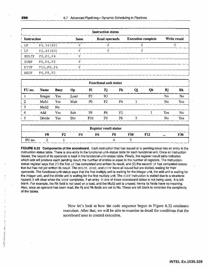
296 6.7 Advanced Pipelining-Dynamic Scheduling in Pipelines
Instruction status
Instruction Issue Read operands Execution complete Write result
LF F6, 34 (R2) ..J ..J ..J ..J
LF F2,45(R3) ..J ..J ..J
MULTF FO,F2,F4 ..J
SUBF F8,F6,F2 ..J
DIVF F10,FO,F6 ..J
ADDF F6,F8,F2
Functional unit status
FU no. Name Busy Op Fi Fj Fk Qi Qk Rj Rk
1 Integer Yes Load F2 R3 No No
2 Multl Yes Mult FO F2 F4 1 No Yes
3 Mult2 No
4 Add Yes Sub F8 F6 F2 1 Yes No
5 Divide Yes Div FlO FO F6 2 No Yes
Register result status
FO F2 F4 F6 FS FlO F12 ... F30
FU no. 2 1 4 5
FIGURE 6.32 Components of the scoreboard. Each instruction that has issued or is pending issue has an entry in the instruction-status table. There is one entry in the functional-unit-status table for each functional unit. Once an instruction issues, the record of its operands is kept in the functional-unit-status table. Finally, the register-result table indicates which unit will produce each pending result; the number of entries is equal to the number of registers. The instructionstatus register says that (1) the first LF has completed and written its result, and (2) the second LF has completed execution but has not yet written its result. The MULTF, SUBF, and D IVF have all issued but are stalled, waiting tor their operands. The functional-unit status says that the first multiply unit is waiting for the integer unit, the add unit is waiting tor the integer unit, and the divide unit is waiting tor the first multiply unit. The ADDF instruction is stalled due to a structural hazard; it will clear when the SUBF completes. If an entry in one of these scoreboard tables is not being used, it is left blank. For example, the Rk field is not used on a load, and the Mult2 unit is unused, hence its fields have no meaning. Also, once an operand has been read, the Rj and Rk fields are set to No. These are left blank to minimize the complexity of the tables.
Now let's look at how the code sequence begun in Figure 6.32 continues execution. After that, we will be able to examine in detail the conditions that the scoreboard uses to control execution.
INTEL Ex.1035.328

Example
Answer
~
Instruction
LF F6,34(R2)
LF F2,45(R3) ---.,_
MULTF FO,F2,F4
SUBF F8,F6,F2
DIVF F10,FO,F6
ADDF F6,F8,F2
FU no. Name Busy
1 Integer No
2 Multl Yes
3 Mult2 No
4 Add' Yes
5 Divide Yes
FO
FU no. 2
Pipelining 297
Assume the following EX cycle latencies for the floating-point functional units: Add is 2 clock cycles, multiply is 10 clock cycles, and divide is 40 clock cycles. Using the code segment in Figure 6.32, and beginning with the point indicated by the instruction status in Figure 6.32, show what the status tables look like when MULTF and DIVF are each ready to go to the write-result state.
There are RAW data hazards from the second LF to MULTF and SUBF, from MULTF to DIVF, and from SUBF to ADDF. There is a WAR data hazard between DIVF and ADDF. Finally, there is a structural hazard on the add functional unit for ADDF. What the tables look like when MULTF and D IVF are ready to go to write result are shown in Figures 6.33 and 6.34, respectively.
Instruction status
Issue Read operands Execution complete Write result
...j ...j ...j ...j
...j ...j ...j ...j
...j ...j ...j
...j ...j ...j ...j
...j
...j ...j ...j
Functional unit status
Op Fi Fj Fk Qi Qk Rj Rk
Mult FO F2 F4 No No
Add F6 F8 F2 No No
Div FlO FO F6 2 No Yes
Register result status
F2 F4 F6 FS FlO F12 ... F30
4 5
FIGURE 6.33 Scoreboard tables just before the MULTF goes to write result. The DIVF has not yet read its operands, since it has a dependence on the result of the multiply. The ADDF has read its operands and is in execution, although it was forced to wait until the SUBF finished to get the functional unit. ADDF cannot proceed to write result because of the WAR hazard on F6, which is used by the DIVF.
INTEL Ex.1035.329

298 6.7 Advanced Pipelining-Dynamic Scheduling in Pipelines
Instruction status
Instruction Issue Read operands Execution complete Write result
LF F6, 34 (R2) --} --} --} --}
LF F2,45(R3) --} --} --} --}
MULTF FO,F2,F4 --} --} --} --}
SUBF F8,F6;F2 --} --} --} --}
DIVF Fl0,FO,F6 --} --} --}
ADDF F6,F8,F2 --} --} --} --}
Functional unit status
FU no. Name Busy Op Fi Fj Fk Qi Qk Rj Rk
1 Integer No
2 Multl No
3 Mult2 No
4 Add No
5 Divide Yes Div FlO FO F6 No No
Register Result status
FO F2 F4 F6 FS FlO F12 ... F30
FU no. 5
FIGURE 6.34 Scoreboard tables just before the DIVF goes to write result. ADDF was able to complete as soon as DIVF passed through read operands and got a copy of F6. Only the DIVF remains to finish.
Instruction status Wait until Bookkeeping
Issue Not busy (FU) and not Busy (FU) f- yes; Result (D) f-FU; Op (FU) f-op; result(D) Fi (FU) f-D; Fj (FU)f-Sl; Fk (FU) f-82;
Qjf-Result (Sl) ; Qkf-Result (S2); Rjf- not Qj; Rkf- not Qk
Read operands Rj and Rk Rjf-No; Rkf-No
Execution complete Functional unit done
Write result 'v'/((Fj(/):;t:Fi(FU) or 'v'f(if Qj(f)=FU then Rj (f) f-Yes); Rj(f)=No) & (Fk(/) 'v' f (if Qk ( f) =FU then Rk ( f) f-Yes); :;t:Fi(FU) or Rk(f)=No)) Result(Fi(FU))f-Clear; Busy (FU) f-No
FIGURE 6.35 Required checks and bookkeeping actions for each step in instruction execution. FU stands for the functional unit used by the instruction, Dis the destination register, 81 and 82 are the source registers, and op is the operation to be done. To access the scoreboard entry named Fj for functional unit FU we use the notation Fj( FU). Result(D) is the value of the result register field for register D. The test on the write-result case prevents the write when there is a WAR hazard. For simplicity we assume that all of the bookkeeping operations are done in one clock cycle.
INTEL Ex.1035.330

Pipelining 299
Now we can see how the scoreboard works in detail by looking at what has to happen for the scoreboard to allow each instruction to proceed. Figure 6.35 shows what the scoreboard requires for each instruction to advance and the bookkeeping action necessary when the instruction does advance.
The costs and benefits of scoreboarding are an interesting question. The CDC 6600 designers measured a performance improvement of 1.7 for FORTRAN programs and 2.5 for hand-coded assembly language. However, this was measured in the days before software pipeline scheduling, semiconductor main memory, and caches (which lower memory-access time). The scoreboard on the CDC 6600 had about as much logic as one of the functional units, which is surprisingly low. The main cost was in the large number of buses-about four times as many as would be required if the machine only executed instructions in order (or if it only initiated one instruction per Execute cycle).
The scoreboard does not handle a few situations as well as it might. For example, when an instruction writes its result, a dependent instruction in the pipeline must wait for access to the register file because all results are written through the register file and never forwarded. This increases the latency and limits the ability of multiple instructions waiting for a result to initiate. WA W hazards would be very infrequent, so the stalls they cause are probably not a significant concern in the CDC 6600. However, in the next section we will see that dynamic ~cheduling offers the possibility of overlapping the execution of multiple iterations of a loop. To do this effectively requires a scheme for handling WA W hazards, which are likely to increase in frequency when multiple iterations are overlapped.
Another Dynamic Scheduling ApproachThe Tomasulo Algorithm
Another approach to parallel execution around hazards was used by the IBM 360/91 floating-point unit. This scheme was credited to R. Tomasulo and is named after him. The IBM 360/91 was completed about three years after the CDC 6600, before caches appeared in commercial machines. IBM's goal was to achieve high floating-1Joint performance from an instruction set and from compilers designed for the entire 360 computer family, rather than for only floatingpoint-intensive applications. Remember that the 360 architecture has only four double-precision floating-point registers, which limits the effectiveness of compiler scheduling; this fact was another motivation for the Tomasulo approach. Lastly, the IBM 360/91 had long memory accesses and long floating-point delays, which the Tomasulo algorithm ,was designed to overcome. At the end of the section, we will see that Tomasulo's algorithm can also support the overlapped execution of multiple iterations of a loop.
We will explain the algorithm, which focuses on the floating-point unit, in the context of a pipelined, floating-point unit for DLX. The primary difference between DLX and the 360 is the presence of register-memory instructions in the latter machine. Because Tomasulo's algorithm uses a load functional unit, no
INTEL Ex.1035.331

300 6.7 Advanced Pipelining-Dynamic Scheduling in Pipelines·
significant changes are needed to add register-memory addressing modes; the primary addition is another bus. The IBM 360/91 also had pipelined functional units, rather than multiple functional units. The only difference between these is that a pipelined unit can start at most one operation per clock cycle. Since there are really no fundamental differences, we describe the algorithm as if there were multiple functional units. The IBM 360/91 could accommodate three operations for the floating-point adder and two for the floating-point multiplier. In addition, up to six floating-point loads, or memory references, and up to three floatingpoint stores could be outstanding. Load data buffers and store data buffers are used for this function. Although we will not discuss the load and store units, we do need to include the buffers for operands.
Tomasulo' s scheme shares many ideas with the CDC 6600 scoreboard, so we assume the reader has understood the scoreboard thoroughly. There are, however, two significant differences. First, hazard detection and execution control are distributed-reservation stations at each functional unit control when an instruction can begin execution at that unit. This function is centralized in the scoreboard on the CDC 6600. Second, results are passed directly to functional units rather than going through the registers. The IBM 360/91 has a common result bus (called the common data bus, or CDB) that allows all units waiting for an operand to be loaded simultaneously. The CDC 6600 writes results into registers, where waiting functional units may have to contend for them. Also, the CDC 6600 has multiple completion buses (two in the floating-point unit), while the IBM 360/91 has only one.
Figure 6.36 shows the basic structure of a Tomasulo-based floating-point unit for DLX; none of the execution control tables are shown. The reservation stations hold instructions that have been issued and are awaiting execution at a functional unit, as well as the information needed to control the instruction once it has begun execution to the unit. The load buffers and store buffers hold data corning from and going to memory. The floating-point registers are connected by a pair of buses to the functional units and by a single bus to the store buffers. All results from the functional units and from memory are sent on the common data bus, which goes everywhere except to the load buffer. All the buffers and reservation stations have tag fields, employed by hazard control.
Before we describe the details of the reservation stations and the algorithm, let's look at the steps an instruction goes through-just as we did for the scoreboard. Since operands are transmitted differently than in a scoreboard, there are only three steps:
1. Issue-Get an instruction from the floating-point operation queue. If the operation is a floating-point operation, issue it if there is an empty reservation station, and send the operands to the reservation station if they are in the registers. If the operation is a load or store, it can issue if there is an available buffer. If there is not an empty reservation station or an empty buffer, then there is a structural hazard and the instruction stalls until a station or buffer is freed.
INTEL Ex.1035.332

Pipelining 301
2. Execute-If one or more of the operands is not yet available, monitor the CDB while waiting for the register to be computed. This step checks for RAW hazards. When both operands are available, execute the operation.
3. Write result-When the result is available, write it on the CDB and from there into the registers and any functional units waiting for this result.
Although these steps are fundamentally similar to those in the scoreboard, there are three important differences. First, there is no checking for WA W and WAR hazards-these are eliminated as a byproduct of the algorithm, as we will see shortly. Second, the CDB is used to broadcast results rather than waiting on the registers. Third, the loads and stores are treated as basic functional units.
The data structures used to detect and eliminate hazards are attached to the reservation stations, the register file, and the load and store buffers. Although different information is attached to different objects, everything except the load
\
From memoty
Load buffers ! 6~---5~---4~---3~---2~---1.._ __ _ ~~o_p-e~ra~ti_o-n~b~us~-o-p-~u-+r~-~~-- ~r~ra
1 I ~ memory
31 I I L I I I L 2 211--+--1--+--•. Reservation 11--1-1--+--1-•• 1
11..,•
1•
1·-·•stations
+ lf'~.~Qd!lr§ • .!;-:!? multloliers;I.
! Common data bus (CDB)
FIGURE 6.36 The basic structure of a DLX FP unit using Tomasulo's algorithm. Floating-point operations are sent from the instruction unit into a queue (called the FLOS, or floating-point operation stack, in the IBM 360/91) when they are issued. The reservation stations include the operation and the actual operands, as well as information used for detecting and resolving hazards. There are load buffers to hold the results of outstanding loads and store buffers to hold the addresses of outstanding stores waiting for their operands. All results from either the FP units or the load unit are put on the common data bus (COB), which goes to the FP register file as well as the reservation stations and store buffers. The FP adders implement addition and subtraction, while the FP multipliers do multiplication and division.
INTEL Ex.1035.333

302 6.7 Advanced Pipelining-Dynamic Scheduling in Pipelines
buffers contains a tag field per entry. The tag field is a four-bit quantity that denotes one of the five reservation stations or one of the six load buffers. The tag field is used to describe which functional unit will produce a result needed as a source operand. Unused values, such as zero, indicate that the operand is already available. In describing the information, the scoreboard names are used wherever this will not lead to confusion. The names used by the IBM 360/91 are also shown. It is important to remember that the tags in the Tomasulo scheme refer to the buffer or unit that will proquce a result; the register number is discarded when an instruction issues to a reservation station.
Each reservation station has six fields:
Op-The operation to perform on source operands S 1 and S2.
Qj,Qk-The reservation stations that will produce the corresponding source operand; a value of zero indicates that the source operand is already available in Vi or Vj, or is unnecessary. The IBM 360/91 calls0 these SINKunit and SOURCEunit.
Vj,Vk-The value of the source operands. These are called SINK and SOURCE on the IBM 360/91. Note that only one of the V field or the Q field is valid for each operand.
Busy-Indicates that this reservation station and its accompanying functional unit are occupied.
The register file and store buffer each have a field, Qi:
Qi-The number of the functional unit that will produce a value to be stored into this register or into memory. If the value of Qi is zero, no currently active instruction is computing a result destined for this register or buffer. For a register, this means the value is given by the register contents.
The load and store buffers each require a busy field, indicating when a buffer is available due to completion of a load or store assigned there. The store buffer also has a field V, the value to be stored.
Before we examine the algorithm in detail, let's see what the system of tables looks like for the following code sequence:
1. LF F6,34(R2)
2. LF F2, 45 (R3)
3. MULTF F0,F2,F4
4 . SUBF F8,F6,F2
5. DIVF F10,FO,F6
6. ADDF F6,F8,F2
We saw what the scoreboard looked like for this program when only the first load had written its result. Figure 6.37 depicts the reservation stations, load and
INTEL Ex.1035.334

Pipelining 303
store buffers, and the register tags. The numbers appended to the names add, mult, and load stand for the tag for that reservation station-Add! is the tag for the result from the first add unit. In addition we have included a central table called "Instruction status." This table is included only to help the reader understand the algorithm; it is not actually a part of the hardware. Instead, the state of each operation that has issued is kept in a reservation station.
There are two important differences from scoreboards that are observable in these tables. First, the value of an operand is stored in the reservation station in one of the V fields as soon as it is available; it is not read from the register file once the instruction has issued. Second, the ADDF instruction has issued. This was blocked in the scoreboard by a structural hazard.
Instruction status
Instruction Issue Execute Write result
LF F6,34(R2) -.J -.J -.J
LF F2,45(R3) -.J -.J
MULTF FO,F2,F4 -.J
SUBF F8,F6,F2 -.J
DIVF Fl0,FO,F6 -.J ·'
ADDF F6,F8,F2 -.J
Reservation stations
Name Busy Op Vj Vk Qj Qk
Addi Yes SUB (Load I) Load2
Add2 Yes ADD Addi Load2
Add3 No
Multi Yes MULT ' (F4) Load2
Mult2 Yes DIV (Loadl) Multi
Register status
Field FO F2 F4 F6 FS FlO F12 ... F30
Qi Multi Load2 Add2 Addi Mult2
Busy Yes Yes No Yes Yes Yes No ... No
FIGURE 6.37 Reservation stations and register tags. All of the instructions have issued, but only the first load instruction has completed and written its result to the CDB. The instruction-status table is not actually present, but the equivalent information is distributed throughout the hardware. The notation (X), where Xis either a register number or a functional unit, indicates that this field contains the result of the functional unit X or the contents of register X at the time of issue. The other instructions are all at reservation stations or, as in the case of instruction 2, completing a memory reference. The load and store buffers are not shown. Load buffer 2 is the only busy load buffer and it is performing on behalf of instruction 2 in the sequence-loading from memory address R3 + 45. There are no stores, so the store buffer is not shown. Remember that an operand is specified by either the Q field or the V field at any time.
INTEL Ex.1035.335

304
Example
Answer
6.7 Advanced Pipelining-Dynamic Scheduling in Pipelines
The big advantages of the Tomasulo scheme are (1) the distribution of the hazard detection logic, and (2) the elimination of stalls for WA W and WAR hazards. The first advantage arises from the distributed reservation stations and the use of the CDB. If multiple instructions are waiting on a single result, and each instruction already has its other operand, then the instructions can be released simultaneously by the broadcast on the CDB. In the scoreboard the waiting instructions must all read their results from the registers when register buses are available.
WA W and WAR hazards are eliminated by renaming registers using the reservation stations. For example, in our code sequence in Figure 6.37 we have issued both the D IVF and the ADDF, even though there is a WAR hazard involving F6. The hazard is eliminated in one of two ways. If the instruction providing the value for the DI VF has completed, then Vk will store the result, allowing DIVF to execute independent of the ADDF (this is the case shown). On the other hand, if the LF had not completed, then Qk would point to the Loadl and the DI VF instruction would be independent of the ADD F. Thus, in either case, the ADD F can issue and begin executing. Any uses of the result of the MULTF would point to the reservation station, allowing the ADDF to complete and store its value into the registers without affecting the DI VF. We'll see an example of the elimination of a WAW hazard shortly. But let's first look at how our earlier example continues execution.
Assume the same latencies for the floating-point functional units as we did for Figure 6.34: Add is 2 clock cycles, multiply is 10 clock cycles, and divide is 40 clock cycles. With the same code segment, show what the status tables look like when the MULTF is ready to go to write result.
The result is shown in the three tables in Figure 6.38. Unlike the example with the scoreboard, ADDF has completed since the operands of DIVF are copied, thereby overcoming the WAR hazard.
INTEL Ex.1035.336

Pipelining 305
Instruction status
Instruction Issue Execute Write result
LF F6, 34 (R2) ..j ..j ..j
LF F2,45(R3) ..j ..j ..j
MULTF FO,F2,F4 ..j ..j • ..j ..j ..j SUBF F8,F6,F2
DIVF F10,FO,F6 I ..j
ADDF F6,F8,F2 ..j ..j ..j
Reservation stations
Name Busy Op Vj Vk Qj Qk
Addi No
Add2 No
Add3 No
Multi Yes MULT (Load2) (F4)
Mult2 Yes DIV (Load I) Multi
Register status
Field FO F2 F4 F6 FS FlO F12 ... F30
Qi Multi Mult2
Busy Yes No No No No Yes No ... No
FIGURE 6.38 Multiply and divide are the only instructions not finished. This is different from the scoreboard case, because the elimination of WAR hazards allowed the ADDF to finish right after the SUBF on which it depended.
Figure 6.39 gives the steps for each instruction to go through. Load and stores are only slightly special. A load can be e;xecuted as soon as it is available. When execution is completed and the CDB is available, a load puts its result on the CDB like any functional unit. Stores receive their values from the CDB or from the register file and execute autonomously; when they are done they tum the busy field off to indicate availability, just like a load buffer or reservation station.
INTEL Ex.1035.337

306 6.7 Advanced Pipelining-Dynamic Scheduling in Pipelines
Instruction status Wait until Action or bookkeeping
Issue Station or buffer empty if (Register[Sl] .Qi *O) {RS[r] .Qjf--Register[Sl] .Qi}
else {RS[r] .Vjf--Sl; RS [ r] . Qj f-- 0} ; if (Register[S2] .Qi*O) {RS[r] .Qkf--Register[S2] .Qi}; else {RS [r] . Vkf-- S2; RS [ r] . Qkf-- 0} RS [r] . Busyf--yes; Register[D] .Qi=r;
Execute (RS[r].Qj=O) and None-operands are in Vj and Vk (RS[r].Qk=O)
Write result Execution completed at r 'efx(if (Register[x] .Qi=r) {Fxf-- result; and CDB available Register [x] . Qif-- 0}) ;
'efx(if (RS [x] . Qj =r) {RS [x] . Vjf-- result; RS [x] .Qj f--0});
Vx(if (RS [x] . Qk=r) {RS [x] . Vkf-- result; RS[x] .Qk f--0});
'efx(if (Store [x] .Qi=r) {Store [ x] . Vf-- result; Store [x] . Qi f-- 0}) ;
RS [ r] . Busyf--NO
FIGURE 6.39 Steps in the algorithm and what is required for each step. For the issuing instruction, D is the destination, S1 and S2 are the sources, and r is the reservation station or buffer that D is assigned to. RS is the reservation-station data structure. The value returned by a reservation station or by the load unit is called the "result." Register is the register data structure, while Store is the store-buffer data structure. When an instruction is issued, the destination register has its Qi field set to the number of the buffer or reservation station to which the instruction is issued. If the operands are available in the registers, they are stored in the V fields. Otherwise, the Q fields are set to indicate the reservation station that will produce the values needed as source operands. The instruction waits at the reservation station until both its operands are available, indicated by zero in the Q fields. The Q fields are set to zero either when this instruction is issued, or when an instruction on which this instruction depends completes and does its write back. When an instruction has finished execution and the COB is available, it can do its write back. All the buffers, registers, and reservation stations whose value of Qj or Qk is the same as the completing reservation station update their values from the COB and mark the Q fields to indicate that values have been received. Thus, the COB can broadcast its result to many destinations in a single clock cycle, and if the waiting instructions have their operands, they can all begin execution on the next clock cycle. For simplicity we assume that all bookkeeping actions are done in a single cycle.
To understand the full power of eliminating WA W and WAR hazards through dynamic renaming of registers, we must look at a loop. Consider the following simple sequence for multiplying the elements of a vector by a scalar in F2:
Loop: LD FO,O(Rl)
MULTD F4,FO,F2
SD O(Rl) ,F4
SUB Rl,Rl,#8
BNEZ Rl,Loop ; branches if Rl*O
With a branch~taken strategy, using reservation stations will allow multiple executions of this loop to proceed at once. This advantage is gained without unrolling the loop-in effect, the loop is unrolled dynamically by the hardware. In
INTEL Ex.1035.338
Pipelining 307
the 360 architecture, the presence of only 4 FP registers would severely limit the use of unrolling. (We will see shortly, when we unroll a loop and schedule it to avoid interlocks, many more registers are required.) Tomasulo's algorithm supports the overlapped execution of multiple copies of the same loop with only a small number of registers used by the program.
Let's assume we have issued all the instructions in two successive iterations of the loop, but none of the floating-point loads/stores or operations has completed. The reservation stations, register-status tables, and load and store buffers at this point are shown in Figure 6.40. (The integer ALU operation is ignored, and it is assumed the branch was predicted as taken.) Once the system reaches this state, two copies of the loop could be sustained with a CPI close to one provided the multiplies could complete in four clock cycles. We will see how compiler techniques can achieve a similar result in Section 6.8.
An additional element that is critical to making Tomasulo's algorithm work is shown in this example. The load instruction from the second loop iteration could easily complete before the store from the first iteration, although the normal sequential order is different. The load and store can safely be done in a different order, provided the load and store access different addresses. This is checked by examining the addresses in the store buffer whenever a load is issued. If the load address matches the store-buffer address, we must stop and wait until the store buffer gets a value; we can then access it or get the value from memory.
This scheme can yield very high performance, provided the cost of branches can be kept small-this is a problem we will look at later in this section. There are also limitations imposed by the complexity of the Tomasulo scheme, which requires a large amount of hardware. In particular, there are many associative stores that must run at high speed, as well as complex control logic. Lastly, the performance gain is limited by the single completion bus (CDB). While additional CDBs can be added, each CDB must interact with all the pipeline hardware, including the reservation stations. In particular, the associative tag-matching hardware would need to be duplicated at all stations for each CDB.
While Tomasulo's scheme may be appealing if the designer is forced to pipeline an architecture that is difficult to schedule code for or has a shortage of registers, the authors believe that the advantages of the Tomasulo approach are limited for architectures that can be efficiently pipelined and statically scheduled with software. However, as available gate counts grow and the limits of software scheduling are reached, we may see dynamic scheduling employed. One possible direction is a hybrid organization that uses dynamic scheduling for loads and stores, while statically scheduling register-register operations.
Reducing Branch Penalties with Dynamic Hardware Prediction
The previous section describes techniques for overcoming data hazards. If control hazards are not addressed, Amdahl's Law predicts, they will limit pipelinedexecution performance. Earlier, we looked at simple hardware schemes for
INTEL Ex.1035.339

308 6. 7 Advanced Pipelining-Dynamic Scheduling in Pipelines
Instruction status
Instruction From iteration Issue Execute Write result
LD FO,O(Rl) 1 -.J -.J
MULTD F4,FO,F2 1 -.J
SD O(Rl),F4 1 -.J
LD FO,O(Rl) 2 -.J -.J
MULTD F4,FO,F2 2 -.J
SD 0(Rl),F4 2 -.J
Reservation stations
Name Busy Fm Vj Vk Qj Qk
Addl No
Add2 No
Add3 No
Multl Yes MULT (F2) Loadl
Mult2 Yes MULT (F2) Load2
Register status
Field FO F2 F4 F6 FS FlO Fl2 ... F30
Qi Load2 Mult2
Busy yes no yes no no no
Store buffers Load buffers
Field Store 1 Store 2 Store 3 Field Load 1 Load2 Load3
Qi Multl Mult2 Address (Rl) (Rl)-8
Busy Yes Yes No Busy Yes Yes No
Address (Rl) (Rl)-8
FIGURE 6.40 Two active iterations of the loop with no instruction having yet completed. Load and store buffers are included, with addresses to be loaded from and stored to. The loads are in the load buffer; entries in the multiplier reservation stations indicate that the outstanding loads are the sources. The store buffers indicate that the multiply destination is their value to store.
dealing with branches (assume taken or not taken) and software-oriented approaches (delayed branches). This section focuses on using hardware to dynamically predict the outcome of a branch-the prediction will change if the branch changes its behavior while the program is running.
The simplest dynamic branch-prediction scheme is a branch-prediction buffer. A branch-prediction buffer is a small memory indexed by the lower por-
INTEL Ex.1035.340

Pipelining 309
tion of the branch instruction address. The memory contains a bit that says whether the branch was recently taken or not. This is the simplest sort of buffer; it has no tags and is useful only to reduce the branch delay when it is longer than the time to compute the possible target PCs. We don't know, in fact, if the prediction is correct-it may have been put there by another branch that has the same low-order address bits. But this doesn't matter. It is assumed to be correct, and fetching begins in the predicted direction. If the branch prediction turns out to be wrong, the prediction bit is inverted.
This simple one-bit prediction scheme has a performance shortcoming: If a branch is almost always taken, then when it is not taken, we will predict incorrectly twice, rather than once. Consider a loop branch whose behavior is taken nine times sequentially, then not taken once. If the next time around it is predicted not taken, the prediction will be wrong. Thus, the prediction accuracy will only be 80%, ·even on branches that are 90% taken. To remedy this, two-bit prediction schemes are often used. In a two-bit scheme, a prediction must miss twice in a row before it is changed. Figure 6.41 shows the finite-state machine for the two-bit prediction scheme.
Not taken
Taken
Not taken
Taken
FIGURE 6.41 This shows the states in a two-bit prediction scheme. By using two bits rather than one, a branch that strongly favors taken or not taken-as many branches dowill be mispredicted only once. The two bits are used to encode the four states in the system.
The branch-prediction buffer can be implemented as a small, special cache accessed with the instruction address during the IF pipe stage, or as a pair of bits attached to each block in the instruction cache and fetched with the instruction (see Section 8.3 in Chapter 8). If the instruction is predicted as a branch and if the branch is predicted as taken, fetching begins from the target as soon as the
INTEL Ex.1035.341

310 6. 7 Advanced Pipelining-Dynamic Scheduling in Pipelines
PC is known. Otherwise, fetching and sequential executing continue. If the prediction turns out to be wrong, the prediction bits are changed as shown in Figure 6.41. While this scheme is useful for most pipelines, the DLX pipeline finds out both whether the branch is taken and what the target of the branch is at the same time. Thus, this scheme does not help for the simple DLX pipeline; we will explore a scheme that can work for DLX a little later. First, let's see how well a prediction buffer works with a longer pipeline.
The accuracy of a two-bit prediction scheme is affected by how often the prediction for each branch is correct and by how often the entry in the prediction buff er matches the branch being executed. When the entry does not match, the prediction bit is used anyway because no better information is available. Even if the entry was for another branch, the guess could be a lucky one. In fact, there is about a 50% probability of being correct, even if the prediction is for some other branch. Studies of branch-prediction schemes have found that two-bit prediction has an accuracy of about 90% when the entry in the buffer is the branch entry. A buffer of between 500 and 1000 entries has a hit rate of 90%. The overall prediction accuracy is given by
Accuracy=(% predicted correctly* % that prediction is for this instruction)+
(%lucky guess)* (1-% that prediction is for this instruction)
Accuracy= (90% * 90%) + (50% * 10%) = 86%
This number is higher than our success rate for filling delayed branches and would be useful in a pipeline with a longer branch delay. Now let's look at a dynamic prediction scheme that is useable for DLX and see how it compares to our branch-delay scheme.
To reduce the branch penalty on DLX, we need to know from what address to fetch by the end of IF. This means we must know whether the as yet undecoded instruction is a branch and, if it is a branch, what the next PC should be. If the instruction is a branch and we know what the next PC should be, we can have a branch penalty of zero. A branch-prediction cache that stores the predicted address for the next instruction after a branch is called a branch-target buffer. Because we are predicting the next instruction address and will send it out before decoding the instruction, we must know whether the fetched instruction is predicted as a taken branch. We also want to know whether the address in the target buffer is for a taken or not-taken prediction, so that we can reduce the time to find a mispredicted branch. Figure 6.42 shows what the branch-target buffer looks like. If the PC of the fetched instruction matches a PC in the buffer, then the corresponding predicted PC is used as the next PC. In Chapter 8 we will discuss caches in much more detail; we will see that the hardware for this branchtarget buffer is similar to the hardware for a cache.
INTEL Ex.1035.342

Pipelining
: PC of instruction to fetch I llook up Predicted PC
. •·· .·. · . .· . ..
.· . .· ..
. .
. ;•·
Number of ·.
entries ... . ..
in .. . . .
:: .. :· :· . . ..
branch- .. ; ..... ·, . target . ·· .. \ . •. ..· buffer .... .· .
: •:. ;.• . .. · : ·.• ... .
. . : . . . ; •: ;. . . :
·.··. ·>.'.·· .. . . .. :.• .. . .. . .• : .• ... •. : . ·· ..
. :·
not predicted to be ?-.. , '""'"""'" ,, branch. Proceed normally
Yes: then instruction is branch and predicted PC should be used as the next PC
. .
.
. .
.
.
Branch predicted taken or untaken
311
FIGURE 6.42 A branch-target buffer. The PC of the instruction being fetched is matched against a set of instruction addresses stored in the first column; these represent the addresses of known branches. If the PC matches one of these entries, then the instruction being fetched is a branch. If it is a branch, then the second field, predicted PC, contains the prediction for the next PC after the branch. Fetching begins immediately at that address. The third field just tracks whether the branch was predicted taken or untaken and helps keep the misprediction penalty small.
If a matching entry is found in the branch-target buffer, fetching begins immediately at the predicted PC. Note that (unlike a branch-prediction buffer) the entry must be for this instruction, because the predicted PC will be sent out before it is known whether this instruction is even a branch. If we did not check whether the entry matched this PC, then the wrong PC would be sent out for instructions that were not branches, resulting in a slower machine. Figure 6.43 shows the steps followed when using a branch-target buffer and when these steps occur in the pipeline. From this we can see that there will be no branch delay if a branch-prediction entry is found in the buffer and is correct. Otherwise, there will be a penalty of at least one clock cycle. In practice, there could be a penalty of two clock cycles because the branch-target buffer must be updated. We could assume that the instruction following a branch or at the branch target is not a branch, and do the update during that instruction time. However, this does complicate the control. Instead, we will take a two-clock-cycle penalty when the branch is not correctly predicted.
INTEL Ex.1035.343
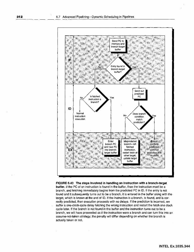
312 6.7 Advanced Pipelining-Dynamic Scheduling in Pipelines
Send out predicted
PC
FIGURE 6.43 The steps involved in handling an instruction with a branch-target buffer. If the PC of an instruction is found in the buffer, then the instruction must be a branch, and fetching immediately begins from the predicted PC in ID. If the entry is not found and it subsequently turns out to be a branch, it is entered in the buffer along with the target, which is known at the end of ID. If the instruction is a branch, is found, and is correctly predicted, then execution proceeds with no delays. If the prediction is incorrect, we suffer a one-clock-cycle delay fetching the wrong instruction and restart the fetch one clock cycle later. If the branch is not found in the buffer and the instruction turns out to be a branch, we will have proceeded as if the instruction were a branch and can turn this into an assume-not-taken strategy; the penalty will differ depending on whether the branch is actually taken or not.
INTEL Ex.1035.344
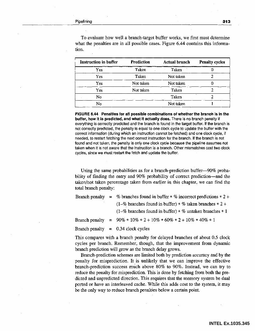
Pipelining 313
To evaluate how well a branch-target buffer works, we first must determine what the penalties are in all possible cases. Figure 6.44 contains this information.
Instruction in buffer Prediction Actual branch Penalty cycles
Yes Taken Taken 0
Yes Taken Not taken 2
Yes Not taken Not taken 0
Yes Not taken Taken 2
No Taken 2
No Not taken 1
FIGURE 6.44 Penalties for all possible combinations of whether the branch is in the buffer, how it is predicted, and what it actually does. There is no branch penalty if everything is correctly predicted and the branch is found in the target buffer. If the branch is not correctly predicted,_ the penalty is equal to one clock cycle to update the buffer with the correct information (during which an instruction cannot be fetched) and one clock cycle, if needed, to restart fetching the next correct instruction for the branch. If the branch is not found and not taken, the penalty is only one clock cycle because the pipeline assumes not taken when it is not aware that the instruction is a branch. Other mismatches cost two clock cycles, since we must restart the fetch and update the buffer.
Using the same probabilities as for a branch-prediction buffer-90% probability of finding the entry and 90% probability of correct prediction-and the taken/not taken percentage taken from earlier in this chapter, we can find the total branch penalty:
Branch penalty = % branches found in buffer * % incorrect predictions * 2 + (1-% branches found in buffer)*% taken branches* 2 +
(1-% branches found in buffer)*% untaken branches* 1
Branch penalty = 90% * 10% * 2 + 10% * 60% * 2 + 10% * 40% * 1
Branch penalty = 0.34 clock cycles
This compares with a branch penalty for delayed branches of about 0.5 clock cycles per branch. Remember, though, that the improvement from dynamic branch prediction will grow as the branch delay grows.
Branch-prediction schemes are limited both by prediction accuracy and by the penalty for misprediction. It is unlikely that we can improve the effective branch-prediction success much above 80% to 90%. Instead, we can try to reduce the penalty for misprediction. This is done by fetching from both the predicted and unpredicted direction. This requires that the memory system be dual ported or have an interleaved cache. While this adds cost to the system, it may be the only way to reduce branch penalties below a certain point.
INTEL Ex.1035.345

314 6.7 Advanced Pipelining-Dynamic Scheduling in Pipelines
We have seen a variety of software-based static schemes and hardware-based dynamic schemes for trying to boost the performance of our pipelined machine. Pipelining tries to exploit the potential for parallelism among sequential instructions. In the ideal case all the instructions would be independent, and our DLX pipeline would exploit parallelism among the five instructions simultaneously in the pipeline. Both the static scheduling techniques of the last section and the dynamic techniques of this section focus on maintaining the throughput of the pipeline at one instruction per clock. In the next section we will look at techniques that attempt to exploit overlap more than by the factor of 5, to which we are restricted with the simple DLX pipeline.
6.8 I Advanced Pipelining-Taking Advantage of More Instruction-Level Parallelism
To improve performance further we would like to decrease the CPI to less than one. But the CPI cannot be reduced below one if we issue only one instruction every clock cycle. The goal of the techniques discussed in this section is to allow multiple instructions to issue in a clock cycle.
As we know from earlier sections, to keep a pipeline full, parallelism among instructions must be exploited by finding sequences of unrelated instructions that can be overlapped in the pipeline. Two related instructions must be separated by a distance equal to the pipeline latency of the fir.st of the instructions. Throughout this section we will assume the latencies shown in Figure 6.45. Branches still have a one-clock-cycle delay. We assume that the functional units are fully pipelined or replicated, and that an operation can be issued on every clock cycle.
As we try to execute more instructions on every clock cycle and try to overlap more instructions, we will need to find and exploit more instruction-level parallelism. Thus, before looking at pipeline organizations that require more parallelism among instructions, let's look at a simple compiler technique that will help create additional parallelism.
Instruction producing result Destination instruction Latency in clocks
FPALUop Another FP ALU op 3
FPALUop Store double 2
Load double FPALU op 1
Load double Store double 0
FIGURE 6.45 Latencies of operations used in this section. The first column shows the originating instruction type. The second column is the type of the consuming instruction. The last column is the separation in clock cycles to avoid a stall. These numbers are similar to the average latencies we would see on an FP unit, like the one we described for DLX in Figure 6.29 (page 289).
INTEL Ex.1035.346
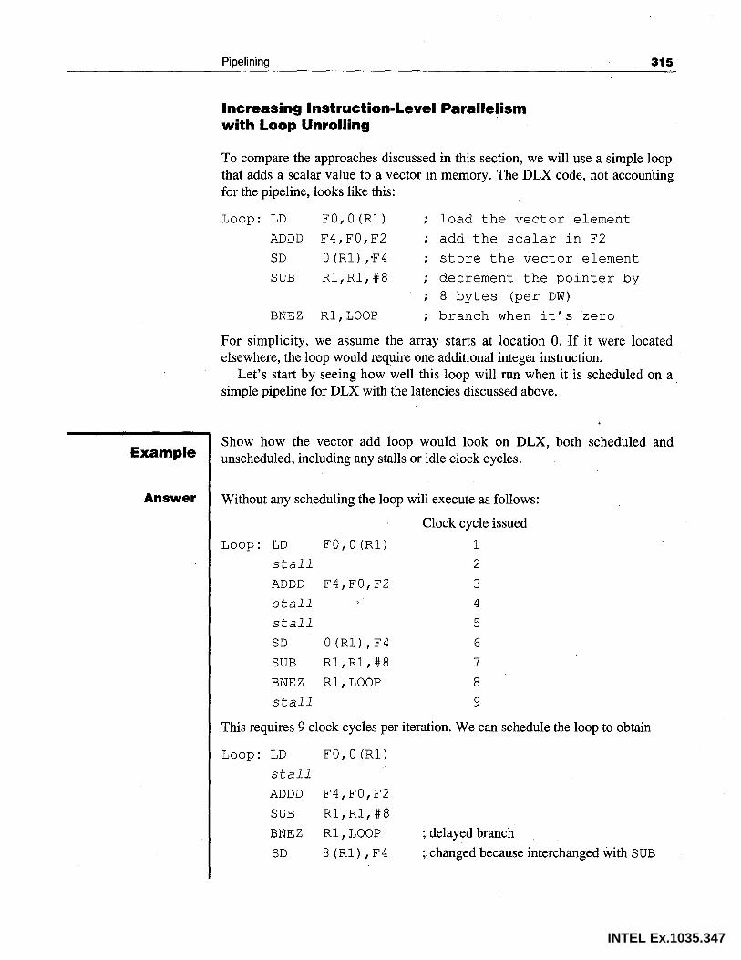
Example
Answer
Pipelining
Increasing Instruction-Level Parallelism with Loop Unrolling
315
To compare the approaches discussed in this section, we will use a simple loop that adds a scalar value to a vector in memory. The DLX code, not accounting for the pipeline, looks like this:
Loop: LD FO,O(Rl) load the vector element
ADDD F4,FO,F2 ; add the scalar in F2
SD 0 (Rl) ,·F4 store the vector element
SUB Rl,Rl,#8 ; decrement the pointer by ; 8 bytes (per DW)
BNEZ Rl,LOOP branch when it's zero
For simplicity, we assume the array starts at location ·O. If it were located elsewhere, the loop would require one additional integer instruction.
Let's start by seeing how well this loop will run when it is scheduled on a simple pipeline for DLX with the latencies discussed above.
Show how the vector add loop would look on DLX, both scheduled and unscheduled, including any stalls or idle clock cycles.
Without any scheduling the loop will execute as follows:
Clock cycle issued
Loop: LD FO,O(Rl) 1
stall 2
ADDD F4,FO,F2 3
stall 4
stall 5
SD 0(Rl),F4 6
SUB Rl,Rl,#8 7
BNEZ Rl,LOOP 8
stall 9
This requires 9 clock cycles per iteration. We can schedule the loop to obtain
Loop: LD
stall
ADDD
SUB
BNEZ
SD
FO,O(Rl)
F4,FO,F2
Rl,Rl,#8
Rl,LOOP
8(Rl),F4
; delayed branch
; changed because interchanged with SUB
INTEL Ex.1035.347

316
Example
Answer
6.8 Advanced Pipelining-;-Taking Advantage of More Instruction-Level Parallelism
Execution time has been reduced from 9 clock cycles to 6. Notice that to create this schedule, the compiler had to determine that it could
swap the SUB and SD by changing the address the SD stored to: The address was 0 (Rl) and is now 8 (Rl). This is not trivial, since most compilers would see that the SD instruction depends on the SUB and would refuse to interchange them. A smarter compiler could figure out the relationship and perform the interchange. The dependence among the LD, ADDD, and SD determines the clock cycle count for this loop.
In the above example, we complete one loop iteration and finish one vector element every 6 clock cycles, but the actual work of operating on the vector element takes just 3 of those 6 clock cycles. The remaining 3 clock cycles consist of loop overhead-the SUB and BNEZ-and a stall. To eliminate these 3 clock cycles we need to get more operations within the loop. A simple scheme for increasing the number of instructions between executions of the loop branch is loop unrolling. This is done by simply replicating the loop body multiple times, adjusting the loop termination code, and then scheduling the unrolled loop. To allow effective scheduling of the loop, we will want to use different registers for each iteration, thus increasing the register count.
Show what our loop looks like unrolled three times (yielding four copies of the loop body), assuming Rl is initially a multiple of 4. Eliminate any obviously redundant computations, and do not reuse any of the registers.
Here is the result after dropping the unnecessary SUB and BNEZ operations duplicated during unrolling.
Loop: LD FO,O(Rl)
ADDD F4,FO,F2
SD 0(Rl),F4 ;drop SUB & BNEZ
LD F6,-8(Rl)
ADDD F8,F6,F2
SD -8 (Rl) , F8 ;drop SUB & BNEZ
LD FlO, -16 (Rl)
ADDD Fl2,Fl0,F2
SD -16(Rl),Fl2 ;drop SUB & BNEZ
LD Fl4,-24(Rl)
ADDD Fl6,Fl4,F2
SD -24(Rl),Fl6
SUB. Rl,Rl,#32
BNEZ Rl,LOOP
INTEL Ex.1035.348

Example
Answer.
Pipelining 317
We have eliminated three branches and three decrements of R 1. The addresses on the loads and stores have been compensated for. Without scheduling, every operation is followed by a dependent operation, and thus will cause a stall. This loop will run in 27 clock cycles-each LD takes 2 clock cycles, each ADDD 3, the branch 2, and all other instructions I-or 6.8 clock cycles for each of the four elements.
Although this unrolled version is currently slower than the scheduled version of the original loop, this will change when we schedule the unrolled loop. Loop unrolling is normally done early in the compilation process, so that redundant computations can be exposed and eliminated by the optimizer.
In real programs we do not normally know the upper bound on the loop. Suppose it is n, and we would like to unroll the loop k times. Instead of a single unrolled loop, we generate a pair of loops. The first executes (n mod k) times and has a body that is the original loop. The unrolled version of the loop is surrounded by an outer loop that iterates (n div k) times. In the above example, unrolling improves the performance of this loop by eliminating overhead instructions, though it increases code size substantially. What will happen to the performance increase when the loop is scheduled on DLX?
Show the unrolled loop in the previous example after it has been scheduled on DLX.
Loop: LD FO,O(Rl)
LD F6,-8(Rl)
LD F10,-16(Rl)
LD Fl4,-24(Rl)
ADDD F4,FO,F2
ADDD F8,F6,F2
ADDD Fl2,Fl0,F2
ADDD F16,F14,F2
SD 0(Rl),F4
SD -8(Rl),F8
SD -16(Rl),F12
SUB Rl,Rl,#32 ;branch dependence
BNEZ Rl,LOOP
SD -24(Rl),F16 ; 8-32 = -24
The execution time of the unrolled loop has dropped to a total of 14 clock cycles, or 3.5 clock cycles per element, compared to 6.8 per element before scheduling.
INTEL Ex.1035.349

318 6.8 Advanced Pipelining-Taking Advantage of More Instruction-Level Parallelism
The gain from scheduling on the unrolled loop is even larger than on the original loop. This is because unrolling the loop exposes more computation that can be scheduled. Scheduling the loop in this fashion necessitates realizing that the loads and stores are independent and can be interchanged.
Loop unrolling is a simple but useful method for increasing the size of straightline code fragments that can be scheduled effectively. This compile-time transformation is similar to what Tomasulo's algorithm does with register renaming and out-of-order execution. As we will see, this is very important in attempts to lower the CPI by issuing instructions at a high rate.
A Superscalar Version of DLX
One method of decreasing the CPI of DLX is to issue more than one instruction per clock cycle. This would allow the instruction-execution rate to exceed the clock rate. Machines that issue multiple independent instructions per clock cycle when they are properly scheduled by the compiler have been called superscalar machines. In a superscalar machine, the hardware can issue a small number (say 2 to 4) of independent instructions in a single clock. However, if the instructions in the instruction stream are dependent or don't meet certain criteria, only the first instruction in sequence will be issued. A machine where the compiler has complete responsibility for creating a package of instructions that can be simultaneously issued, and the hardware does not dynamically make any decisions about multiple issue, should probably be regarded as a type of VLIW (very long instruction word), which we discuss in the next section.
What would the DLX machine look like as a superscalar? Let's assume two instructions issued per clock cycle. One of the instructions could be a load, store, branch, or integer ALU operation, and the other could be any floating-point operation. As we will see, issue of an integer operation in parallel with a floating-point operation is much simpler and less demanding than arbitrary dual issue.
Issuing two instructions per cycle will require fetching and decoding 64 bits of instructions. To keep the decoding simple, we could require that the instructions be paired and aligned on a 64-bit boundary, with the integer portion appearing first. Figure 6.46 shows how the instructions look as they go into the pipeline in pairs. This table does not address how the floating-point operations extend the EX cycle, but it is no different in the superscalar case than it was for the ordinary DLX pipeline; the concepts of Section 6.6 apply directly. With this pipeline, we have substantially boosted the rate at which we can issue floatingpoint instructions. To make this worthwhile, however, we need either pipelined floating-point units or multiple independent units. Otherwise, floating-point instructions can only be fetched, and not issued, since all the floating units will be busy.
INTEL Ex.1035.350