Ethernet Media Access Controller - Intel
61
17 Ethernet Media Access Controller 2014.08.18 a10_54017 Subscribe Send Feedback The hard processor system (HPS) provides three Ethernet media access controller (EMAC) peripherals. Each EMAC can be used to transmit and receive data at 10/100/1000 Mbps over Ethernet connections in compliance with the IEEE 802.3 specification. The EMACs are instances of the Synopsys ® DesignWare ® Universal 10/100/1000 Ethernet MAC (version 3.72a). The EMAC has an extensive memory-mapped control and status register (CSR) set, which can be accessed by the ARM Cortex ™ -A9 ® MPCore ™ . In addition, the three EMACs may be used directly by the FPGA fabric through the Synopsys Application Interface (Referred to as the Application Interface for the rest of this document). For an understanding of this chapter, you should be familiar with the basics of IEEE 802.3 media access control (MAC). (1) Related Information IEEE Standards Association website For complete information about IEEE 802.3 MAC, refer to the IEEE 802.3 2008 Part 3: Carrier sense multiple access with Collision Detection (CSMA/CD) Access Method and Physical Layer Specifications, available on the IEEE Standards Association website. Features of the Ethernet MAC MAC • IEEE 802.3-2008 compliant • Data rates of 10/100/1000 Mbps • IEEE 802.3x flow control in full-duplex • Full duplex and half duplex modes • IEEE 802.3x flow control automatic transmission of zero-quanta pause frame on flow control input deassertion (1) Portions © 2014 Synopsys, Inc. Used with permission. All rights reserved. Synopsys & DesignWare are registered trademarks of Synopsys, Inc. All documentation is provided "as is" and without any warranty. Synopsys expressly disclaims any and all warranties, express, implied, or otherwise, including the implied warranties of merchantability, fitness for a particular purpose, and non-infringement, and any warranties arising out of a course of dealing or usage of trade. †Paragraphs marked with the dagger (†) symbol are Synopsys Proprietary. Used with permission. ISO 9001:2008 Registered © 2014 Altera Corporation. All rights reserved. ALTERA, ARRIA, CYCLONE, ENPIRION, MAX, MEGACORE, NIOS, QUARTUS and STRATIX words and logos are trademarks of Altera Corporation and registered in the U.S. Patent and Trademark Office and in other countries. All other words and logos identified as trademarks or service marks are the property of their respective holders as described at www.altera.com/common/legal.html. Altera warrants performance of its semiconductor products to current specifications in accordance with Altera's standard warranty, but reserves the right to make changes to any products and services at any time without notice. Altera assumes no responsibility or liability arising out of the application or use of any information, product, or service described herein except as expressly agreed to in writing by Altera. Altera customers are advised to obtain the latest version of device specifications before relying on any published information and before placing orders for products or services. www.altera.com 101 Innovation Drive, San Jose, CA 95134
-
Upload
khangminh22 -
Category
Documents
-
view
1 -
download
0
Transcript of Ethernet Media Access Controller - Intel

17Ethernet Media Access Controller
2014.08.18
a10_54017 Subscribe Send Feedback
The hard processor system (HPS) provides three Ethernet media access controller (EMAC) peripherals.Each EMAC can be used to transmit and receive data at 10/100/1000 Mbps over Ethernet connections incompliance with the IEEE 802.3 specification. The EMACs are instances of the Synopsys® DesignWare®Universal 10/100/1000 Ethernet MAC (version 3.72a).
The EMAC has an extensive memory-mapped control and status register (CSR) set, which can be accessedby the ARM Cortex™-A9®MPCore™. In addition, the three EMACs may be used directly by the FPGA fabricthrough the Synopsys Application Interface (Referred to as the Application Interface for the rest of thisdocument).
For an understanding of this chapter, you should be familiar with the basics of IEEE 802.3 media accesscontrol (MAC). (1)
Related InformationIEEE Standards Association websiteFor complete information about IEEE 802.3 MAC, refer to the IEEE 802.3 2008 Part 3: Carrier sensemultipleaccess with Collision Detection (CSMA/CD) Access Method and Physical Layer Specifications, available onthe IEEE Standards Association website.
Features of the Ethernet MAC
MAC• IEEE 802.3-2008 compliant• Data rates of 10/100/1000 Mbps• IEEE 802.3x flow control in full-duplex• Full duplex and half duplex modes• IEEE 802.3x flow control automatic transmission of zero-quanta pause frame on flow control input
deassertion
(1) Portions© 2014 Synopsys, Inc. Usedwith permission. All rights reserved. Synopsys&DesignWare are registeredtrademarks of Synopsys, Inc. All documentation is provided "as is" andwithout anywarranty. Synopsys expresslydisclaims any and all warranties, express, implied, or otherwise, including the implied warranties ofmerchantability, fitness for a particular purpose, and non-infringement, and any warranties arising out of acourse of dealing or usage of trade.
†Paragraphs marked with the dagger (†) symbol are Synopsys Proprietary. Used with permission.
ISO9001:2008Registered
© 2014 Altera Corporation. All rights reserved. ALTERA, ARRIA, CYCLONE, ENPIRION, MAX, MEGACORE, NIOS, QUARTUS and STRATIX wordsand logos are trademarks of Altera Corporation and registered in the U.S. Patent and Trademark Office and in other countries. All otherwords and logos identified as trademarks or service marks are the property of their respective holders as described atwww.altera.com/common/legal.html. Altera warrants performance of its semiconductor products to current specifications in accordance withAltera's standard warranty, but reserves the right to make changes to any products and services at any time without notice. Altera assumesno responsibility or liability arising out of the application or use of any information, product, or service described herein except as expresslyagreed to in writing by Altera. Altera customers are advised to obtain the latest version of device specifications before relying on any publishedinformation and before placing orders for products or services.
www.altera.com
101 Innovation Drive, San Jose, CA 95134

• Optional forwarding of received pause control frames to the user• Packet bursting and frame extension in 1000 Mbps half-duplex• IEEE 802.3x flow control in full-duplex• Back-pressure support for half-duplex• IEEE 1588-2002 and IEEE 1588-2008 precision networked clock synchronization• IEEE 802.3-az, version D2.0 for Energy Efficient Ethernet (EEE)• IEEE 802.1Q virtual local area network (VLAN) tag detection for reception frames• Preamble and start-of-frame data (SFD) insertion in transmit and deletion in receive paths• Automatic cyclic redundancy check (CRC) and pad generation controllable on a per-frame basis• Options for automatic pad/CRC stripping on receive frames• Programmable frame length supporting standard and jumbo Ethernet frames (with size up to 9.6 KB )• Programmable inter-frame gap (IFG), from 40- to 96-bit times in steps of eight• Preamble of up to 1 byte supported• Supports internal loopback asychronous FIFO on the GMII/MII for debugging• Supports a variety of flexible address filtering modes
• Up to 31 additional 48-bit perfect destination address (DA) filters with masks for each byte• Up to 31 48-bit source address (SA) comparison check with masks for each byte• 256-bit hash filter (optional) for multicast and uni-cast DAs• Option to pass all multicast addressed frames• Promiscuous mode support to pass all frames without any filtering for network monitoring• Passes all incoming packets (as per filter) with a status report
PHY Interface• Reduced Gigabit Media Independent Interface (RGMII) for 10/100/1000• Gigabit Media Independent Interface (GMII) through the FPGA fabric• Serial Gigabit Media Independent Interface (SGMII) supported through the GMII to FPGA fabric• Media Independent Interface (MII) through the FPGA fabric• Management Data Input/Output (MDIO) (IEEE 802.3) or I2C PHY management interface
DMA Interface• 32-bit interface• Programmable burst size for optimal bus utilization• Single-channel mode transmit and receive engines• Byte-aligned addressing mode for data buffer support• Dual-buffer (ring) or linked-list (chained) descriptor chaining• Descriptors can each transfer up to 8 KB of data• Independent DMA arbitration for transmit and receive with fixed priority or round robin
Management Interface• 32-bit host interface to CSR set• Comprehensive status reporting for normal operation and transfers with errors• Configurable interrupt options for different operational conditions• Per-frame transmit/receive complete interrupt control• Separate status returned for transmission and reception packets
Ethernet Media Access ControllerAltera Corporation
Send Feedback
a10_54017PHY Interface17-2 2014.08.18

Application InterfacePending
AccelerationTransmit and receive checksum offload for transmission control protocol (TCP), user datagram protocol(UDP), or Internet control message protocol (ICMP) over Internet protocol (IP)
EMAC Block Diagram and System IntegrationFigure 17-1: EMAC System Integration
PHY
EMAC0PHYMDIO
TMSTP APDMACSR
EMAC1
EMAC1
I2C(For Ethernet)
L3Interconnect
PinMultiplexer
HPS
3 3GMII/MII/MDIO
RGMII/RMII
MDIO/I2C
AXI
APB
LegendTMSTP = TimestampAP = Synopsys Application Interface
PHY Transceiver
PHY
FPGA Fabric
EMAC Overview
Each EMAC is an internal bus master and sends Ethernet packets to and from the system Interconnect. TheSynopsys protocol is a descriptor ring protocol, where the descriptor contains an address to a buffer to storethe packet data. An application can route Ethernet packets directly to the FPGA Fabric through theApplication Interface.
Each EMAC has an MDIO Management port to send commands to the external PHY. This port can beimplemented using the I2C modules in the HPS or the EMAC's MDIO interface.
Each EMAC has an IEEE 1588 Timestamp interface with 1 micron resolution. The ARM Cortex-A9microprocessor unit (MPU) susbsystem can use it to maintain synchronization between the time countersthat are internal to the three MACs. The clock reference for the timestamp can be provided by the ClockManager (emac_ptp_clk) or the FPGA fabric (f2h_emac_ptp_ref_clk). The clock reference is selected bythe ptp_clk_sel bit in the emac_global register in the system manager.
Altera CorporationEthernet Media Access Controller
Send Feedback
17-3Application Interfacea10_540172014.08.18

All three EMACs must use the same clock reference. In addition, EMAC0 can be configured toprovide the timestamp for EMAC1, EMAC2, or both by setting the ptp_ref_sel bit in the emacnregister.
Note:
EMAC to RGMII Interface
Table 17-1: External PHY Datapath In/Out Interface
DescriptionWidthIn/OutEMAC Port
This signal provides the transmitclock for RGMII (125/25/2.5 MHzin 1G/100M/10Mbps) andRMII (50MHz in 100M / 10 Mbps). All PHYtransmit signals generated by theEMAC are synchronous to thisclock.
1OutTransmit Clock
This is a group of eight transmitdata signals are driven by the MAC.Bits [3:0] provide the RGMIItransmit data, and bits [1:0] providethe RMII transmit data. Unused bitsin the RGMII and RMII interfaceconfiguration are tied to low. InRGMII mode, the data bus carriestransmit data at double rate and aresampled on both the rising andfalling edges of the transmit clock.The validity of the data is qualifiedwith phy_txen_o.
8OutPHY Transmit Dataphy_txd_o
This signal is driven by the EMACcomponent, and in RGMII modeacts as the control signal (rgmii_tctl)for the transmit data, and is drivenon both edges of the transmit clock,phy_txclk_o. In RMII mode, thissignal is high to indicate valid data.
1OutPHY Transmit DataEnable
phy_txen_o
In RGMII mode, this clockfrequency is 125/25/2.5 MHz in 1G/100 M/10 Mbps modes. It isprovided by the external PHY. AllPHY signals received by the EMACare synchronous to this clock. InRMII mode, both interfaces use thephy_txclk_o as the clock reference.
1InReceive Clockphy_clk_rx_i
Ethernet Media Access ControllerAltera Corporation
Send Feedback
a10_54017EMAC to RGMII Interface17-4 2014.08.18

DescriptionWidthIn/OutEMAC Port
These eight data signals are receivedfrom the PHYand carry receive dataat double rate with bits[3:0] valid onthe rising edge of phy_rxclk_i, andbits[7:4] valid on the falling edge ofphy_rxclk_i. The validity of thedata is qualified with phy_rxdv_i.
8InPHY Receive Dataphy_rxd_i
This signal is driven by PHY andfunctions are the receive controlsignal used to qualify the datareceived on phy_rxd_i. This signalis sampled on both edges of theclock.
1InPHYReceiveDataValidphy_rxdv_i
EMAC to FPGA GMII and MII PHY Interface
Table 17-2: EMAC to FPGA PHY Interface Signals
DescriptionWidthIn/OutSignal Name
This is the transmit clock (2.5MHz/25MHz) provided by theMII PHYsonly. This clock comes from theFPGA Interface and is used for TXdata capture. This clock is not usedin GMII mode.
1InTransmit Clockclk_tx_i
For GMII, this signal is the transmitclock output to the PHY to sampledata.
For MII this clock is unused.
1OutTransmit Clock Outputphy_txclk_o
These are a group of eight transmitdata signals driven by the MAC.
• All eight bits provide the GMIItransmit data byte. For the lowerspeed MII operation, only thelow 4 bits are used. The validityof the data is qualified withphy_txen_o and phy_txer_o.Synchronous to: phy_ clk_tx_o.
8OutPHY Transmit Dataphy_txd_o
This signal is driven by the EMACcomponent and is used in GMIImode to indicatewhenhigh indiatesthat valid data is being transmittedon the clk_tx_o bus.
1OutPHY Transmit DataEnable
phy_txen_o
Altera CorporationEthernet Media Access Controller
Send Feedback
17-5EMAC to FPGA GMII and MII PHY Interfacea10_540172014.08.18

DescriptionWidthIn/OutSignal Name
This signal is driven by the MACandwhen high, indicates a transmiterror or carrier extension on thephy_txd bus. Also used for signalingof low power states in EnergyEfficient Ethernet operation.
1OutPHY Transmit Errorphy_txer_o
Transmit clock reset output to theFPGA fabric: This is the internalsynchronized reset to clk_tx_intoutput from the EMAC. May beused by logic implemented in theFPGA fabric as desired.
1OutTransmit Clock Resetoutput
rst_clk_tx_n_o
Receive clock from external PHY.
For GMII, the clock frequency is125MHz. ForMII, the receive clockis 25 MHz for 100 Mpbs and 2.5MHz for 10 Mpbs.
1InReceive Clockphy_clk_rx_i
This is a bundle of eight data signalsreceived from the PHY. In GMIImode, all 8 bits provide the GMIIreceive data byte. The validity of thedata is qualified with phy_rxdv_iand phy_rxer_i. For lower speedMII operation, only the bottom 4bits are used. Synchronous to:phy_ clk_rx_i
8InPHY Receive Dataphy_rxd_i
This signal is driven by PHY and inGMII mode, it indicates when highthat the data on the phy_rxd bus isvalid. It remains asserted continu-ously from the first recovered byteof the frame through the finalrecovered byte.
1InPHYReceiveDataValidphy_rxdv_i
This signal indicates an error orcarrier extension (GMII) in thereceived frame. Synchronous to:phy_clk_rx_i, This signal is not usedin RGMII mode.
1InPHY Receive Errorphy_rxer_i
Receive clock reset output.1OutReceive clock resetoutput.
rst_clk_rx_n_o
Ethernet Media Access ControllerAltera Corporation
Send Feedback
a10_54017EMAC to FPGA GMII and MII PHY Interface17-6 2014.08.18

DescriptionWidthIn/OutSignal Name
This signal is asserted by the PHYwhen either the transmit or receivemedium is not idle. The PHY de-asserts this signal when bothtransmit and receive interfaces areidle. This signal is not synchronousto any clock.
1InPHY Carrier Sensephy_crs_i
This signal, valid only whenoperating in half duplex, is assertedby the PHY when a collision isdetected on themedium.This signalis not synchronous to any clock.
1InPHY Collision Detectphy_col_i
EMAC to FPGA Application InterfaceATI = Application Transmit Interface and ARI = Application Receive Interface
DescriptionWidthIn/OutSignal Name
Clock Reference for the ATI andARI interfaces. All signals aresynchronous to this clock.
1InFPGA to Applicationclock
f2sh_ap_clk
This signal indicates, that theapplication is ready to transfer dataof the frame. This is qualified byemac_ati_val_i .
1InStart of Frameemac_ati_sof_i
When this signal is asserted, itdisables the addition of FCS to theframe by theMAC.This signal valueis sampled only whenemac_ati_sof_i is active. This signalis qualified by emac_ati_val_i.
1InDisable CRCemac_ati_discrc_i
This signal disables the addition ofpads to the frame by the MAC. Thissignal value is sampled only whenemac_ati_sof_i is active. This signalis qualified by emac_ati_val_i.
1InDisable Pademac_ati_dispad_i
This signal indicates that the currentdata transferred is the last dataphase. This signal is qualified byemac_ati_val_i.
1InEnd of Frameemac_ati_eof_i
Altera CorporationEthernet Media Access Controller
Send Feedback
17-7EMAC to FPGA Application Interfacea10_540172014.08.18

DescriptionWidthIn/OutSignal Name
This signal is qualified byemac_ati_val_i and emac_ati_eof_i.When emac_ati_eof_i is low,emac_ati_be_i is taken as all ones.Encoding:
• 11: 4 bytes valid
• 10: LS 3 bytes valid
• 01: LS 2 bytes valid
• 00: LS 1 byte valid
2InNumber of Valid ByteLanes
emac_ati_be_i
This signal qualifies all the frametransmission control signals anddata on ATI interface.
1InATI Validemac_ati_val_i
Frame data from the application.The LSB lane emac_ati_data_i[7:0]is the first byte transmitted by thecore.
32InApplication Dataemac_ati_data_i
When asserted, this signal indicatesthe MTL FIFO is ready to acceptadditional data from the application.This signal is de-asserted when TXFIFO is being flushed or when theTX FIFO is full.
1OutATI Readyemac_ati_rdy_o
This signal qualifies the status wordon emac_ati_txstatus_o. This signalis asserted, when a valid status wordis available in the status FIFO.
1OutValid Transmit Statusemac_ati_txstatus_val_o
Transmit frame status wordtransferred to the application. Thesebits are equivalent to [18:0] of firstword of Enhanced Descriptorformat. See Section 8.4.1 inSynopsys DWC Datasheet.
18OutTransmit Status Workemac_ati_txstatus_o
The acknowledgment signal fromthe application, indicating that thetransmit word has been accepted.
1InATI Acknowledgmentemac_ati_ack_i
When asserted, this signal indicatesthe TX FIFO has enough space toaccommodate the number of databeats as indicated by emac_ati_pbl_i(in previous clock cycle).
1Outemac_ati_tx_watermark_o
Ethernet Media Access ControllerAltera Corporation
Send Feedback
a10_54017EMAC to FPGA Application Interface17-8 2014.08.18

DescriptionWidthIn/OutSignal Name
Indicates the space requested by theapplication in terms of beats (4bytes).
9InNumber of Beatsemac_ati_pbl_i
This signal is sampled only whenemac_ati_val_i and emac_ati_sof_iare high.
These input signals control theinsertion of checksums in Ethernetframes that encapsulate TCP, UDP,or ICMP over IPv4 or IPv6, asfollows:
• 00: Do nothing. BypassChecksum
• 01: Insert IPv4Header checksum• 10: Insert TCP, UDP, or ICMP
checksum with psudo-headerchecksumavailable inChecksumfield. IPv4 header is also insertedif IPv4 packet
• 11: Insert TCP, UDP, or ICMPchecksum (fully calculated)
2InSideband ChecksumOffload Control.
emac_ati_chksum_ctrl_i
When set high, instructs the MACto capture the timestamp for thetransmit frame. The applicationshould assert it only for the PTPframes that require timestamping.This signal is sampled only whenemac_ati_sof_i and emac_ati_val_iare high.
1InTransmit EnableTimestamping
emac_ati_ena_timestamp_i
This bus provides the timestamp ofthe transmitted frame for which thestatus is available on theemac_ati_txstatus_o bus. The valueon this bus is qualified byemac_ati_txstatus_val_o signal.
64OutTransmit FrameTimestamp
emac_ati_timestamp_o
This signal indicates that the currentdata transferred to the applicationcorresponds to the first data phaseof the frame.
1OutStart of Frameemac_ari_sof_o
This signal indicates that the currentdata transferred to the applicationcorresponds to the last data phaseof the frame.
1OutEnd of Frameemac_ari_eof_o
Altera CorporationEthernet Media Access Controller
Send Feedback
17-9EMAC to FPGA Application Interfacea10_540172014.08.18

DescriptionWidthIn/OutSignal Name
When asserted, this signal qualifiesthe data and other control signals.
1OutARI Validemac_ari_val_o
Frame data from the RX FIFO tothe application. The LSB laneari_data_o[7:0] is the first bytereceived by the core.
32OutFrame Dataemac_ari_data_o
Indicates the number of valid bytesin the last data phase transfer.Encoding:
• 11: 4 bytes valid
• 10: LS 3 bytes valid
• 01: LS 2 bytes valid
• 00: LS 1 byte valid
2OutNumber of Valid ByteLanes
emac_ari_be_o
The acknowledgment from theapplication indicates that thecurrent data that includes theReceive status has been accepted bythe host.
1InARI Acknowledgmentemac_ari_ack_i
Indicates that the emac_ari_data_obus contains the receive status to theapplication. These bits areequivalent to [30:0] of first word ofEnhanced Descriptor format.
1OutValid Receive Statusemac_ari_rxstatus_val_o
When asserted, this signal indicatesthat the RX FIFO has enough datato generate the number of beats (4bytes) as requested throughemac_ari_pbl_i.
1OutReceive Watermarkemac_ari_rx_watermark_o
When asserted, this signal indicatesthe number of beats of datarequested by the application fromthe RX FIFO.
9InNumber of Beatsemac_ari_pbl_i
When asserted, this signal directsthe application to flush the currentframe that is being transferred tothe application.
1InFrame Flush Requestemac_ari_frame_flush_i
When asserted for 2 clock cycles,this signal indicates that a validtimestamp value is available on theARI data bus (emac_ari_data_o).
1OutReceive TimestampValid
emac_ari_timestamp_val_o_o
Ethernet Media Access ControllerAltera Corporation
Send Feedback
a10_54017EMAC to FPGA Application Interface17-10 2014.08.18
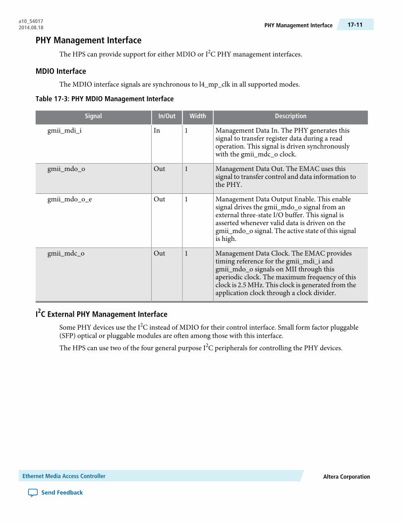
PHY Management InterfaceThe HPS can provide support for either MDIO or I2C PHY management interfaces.
MDIO Interface
The MDIO interface signals are synchronous to l4_mp_clk in all supported modes.
Table 17-3: PHY MDIO Management Interface
DescriptionWidthIn/OutSignal
Management Data In. The PHY generates thissignal to transfer register data during a readoperation. This signal is driven synchronouslywith the gmii_mdc_o clock.
1Ingmii_mdi_i
Management Data Out. The EMAC uses thissignal to transfer control and data information tothe PHY.
1Outgmii_mdo_o
Management Data Output Enable. This enablesignal drives the gmii_mdo_o signal from anexternal three-state I/O buffer. This signal isasserted whenever valid data is driven on thegmii_mdo_o signal. The active state of this signalis high.
1Outgmii_mdo_o_e
Management Data Clock. The EMAC providestiming reference for the gmii_mdi_i andgmii_mdo_o signals on MII through thisaperiodic clock. The maximum frequency of thisclock is 2.5 MHz. This clock is generated from theapplication clock through a clock divider.
1Outgmii_mdc_o
I2C External PHY Management Interface
Some PHY devices use the I2C instead of MDIO for their control interface. Small form factor pluggable(SFP) optical or pluggable modules are often among those with this interface.
The HPS can use two of the four general purpose I2C peripherals for controlling the PHY devices.
Altera CorporationEthernet Media Access Controller
Send Feedback
17-11PHY Management Interfacea10_540172014.08.18
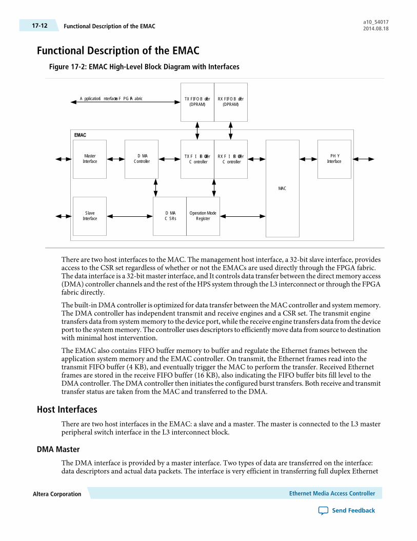
Functional Description of the EMACFigure 17-2: EMAC High-Level Block Diagram with Interfaces
MasterInterface
DMAController
TX FIFO BufferController
RX FIFO BufferController
RX FIFO Buffer(DPRAM)
MAC
PHYInterface
EMAC
SlaveInterface
Operation ModeRegister
DMACSRs
TX FIFO Buffer(DPRAM)
Application Interface to FPGA Fabric
There are two host interfaces to the MAC. The management host interface, a 32-bit slave interface, providesaccess to the CSR set regardless of whether or not the EMACs are used directly through the FPGA fabric.The data interface is a 32-bitmaster interface, and It controls data transfer between the directmemory access(DMA) controller channels and the rest of theHPS system through the L3 interconnect or through the FPGAfabric directly.
The built-inDMAcontroller is optimized for data transfer between theMAC controller and systemmemory.The DMA controller has independent transmit and receive engines and a CSR set. The transmit enginetransfers data from systemmemory to the device port, while the receive engine transfers data from the deviceport to the systemmemory. The controller uses descriptors to efficientlymove data from source to destinationwith minimal host intervention.
The EMAC also contains FIFO buffer memory to buffer and regulate the Ethernet frames between theapplication system memory and the EMAC controller. On transmit, the Ethernet frames read into thetransmit FIFO buffer (4 KB), and eventually trigger the MAC to perform the transfer. Received Ethernetframes are stored in the receive FIFO buffer (16 KB), also indicating the FIFO buffer bits fill level to theDMAcontroller. TheDMAcontroller then initiates the configured burst transfers. Both receive and transmittransfer status are taken from the MAC and transferred to the DMA.
Host InterfacesThere are two host interfaces in the EMAC: a slave and a master. The master is connected to the L3 masterperipheral switch interface in the L3 interconnect block.
DMA Master
The DMA interface is provided by a master interface. Two types of data are transferred on the interface:data descriptors and actual data packets. The interface is very efficient in transferring full duplex Ethernet
Ethernet Media Access ControllerAltera Corporation
Send Feedback
a10_54017Functional Description of the EMAC17-12 2014.08.18

packet traffic. Read and write data transfers from different DMA channels can be performed simultaneouslyon this port. The only exceptions to this are transmit descriptor reads andwrite-backs, which cannot happensimultaneously.
DMA transfers are split into a software configurable number of burst transactions on the interface. TheAXI_Bus_Mode register in the dmagrp group is used to configure bursting behavior.
The interface assigns a unique ID for each DMA channel and also for each read DMA or write DMA requestin a channel. Data transfers with distinct IDs can be reordered and interleaved.
Write data transfers are generally performed as posted writes with OK responses returned as soon as thesystem interconnect has accepted the last beat of a data burst. Descriptors (status or timestamp) howeverare always transferred as non-posted writes in order to prevent race conditions with the transfer completeinterrupt logic.
The slave may issue an error response. When that happens, the EMAC disables the DMA channel thatgenerated the original request and asserts an interrupt signal. The host must reset the EMAC with a hard orsoft reset to restart the DMA to recover from this condition.
The EMAC supports up to 16 outstanding transactions on the interface. Buffering outstanding transactionssmooths out back pressure behavior improving throughput when resource contention bottlenecks ariseunder high system load conditions.
Cache Control Interface
The system manager provides the values for the master cache outputs through this interface.
To configure EMAC DMA controller to perform cacheable accesses, configure the cache bits in the systemmanager. Register bits should be accessed only when the master interface is guaranteed to be in an inactivestate.
Related InformationSystem ManagerFormore information, refer to the SystemManager chapter in theHard Processor SystemTechnical ReferenceManual.
System Manager Configuration Interface
The SystemManager configures several static EMAC functions as shown in the table below, SystemManagerConfiguration Interface. Software must configure these functions appropriately prior to using the EMACmodule.
Table 17-4: System Manager Control Settings
DescriptionFunction
Select RESET, RGMII, RMII or GMII/MII as the PHY interface. The RESETmode is the default out of reset and configures the EMAC to use an internalclock rather than depending on a PHY to provide and active clock. TheRESET mode cannot be used with any PHY, and another setting must beprogrammed before attempting to communicate with a PHY.
PHY Select
This field selects if the Timestamp reference is internally or externallygenerated. EMAC0 must be set to Internal Timestamp. EMAC0 may be themaster to generate the timestamp for EMAC1 and EMAC2. EMAC1 andEMAC2 may be set to either Internal or External.
PTP Timestamp ReferenceSelect
Altera CorporationEthernet Media Access Controller
Send Feedback
17-13Cache Control Interfacea10_540172014.08.18

DescriptionFunction
Selects the source of the PTP reference clock between emac_ptp_clk fromthe Clock Manager or f2h_emac_ptp_ref_clk from the FPGA Fabric. Allthree EMAC modules must use the same reference clock.
PTP Timestamp Clock Select
Static fields to drive the ARCACHE/AWCACHE signals for the AXI DMAbus.
AXI Cache Settings
Selects the source of the Application clock for the datapath. The clock sourcecan be either l4_mp_clk for normal operation or f2h_ap_clk if theApplicationInterface is enabled to the FPGA fabric.
Application Datapath ClockSelect
Enables logic from the FPGA except for the Application Interface. This signalis only for safety to prevent spurious inputs from the FPGA before the FPGAis configured.
FPGA Interface Enable
Enable the Application interface to and from the FPGA Fabric.FPGASwitch Interface Enable
Related InformationSystem ManagerFormore information, refer to the SystemManager chapter in theHard Processor SystemTechnical ReferenceManual.
Transmit and Receive Data FIFO BuffersEachEMACcomponent has associated transmit and receive data FIFObuffer instances. TheRXFIFObufferinstance is 4096 x 42 bits and the TX FIFO buffer instance is 1024 x 42 bits. The FIFO buffer word consistsof:
• Data: 32 bits• Sideband:
• Byte enables (BE): 2 bits• End of frame (EOF): 1 bit• Error correction code (ECC): 7 bits
The data and sideband are protected by the 7-bit single error correct, double error detect (SEC-DED) codeword.
The FIFO buffer RAMs have ECC enable, error injection and status pins. The enable and error injectionpins are inputs driven by the system manager. The status pins are outputs driven to the MPU subsystem.
Error Checking and CorrectionEach EMAC has a 4 KB TX FIFO buffer and a 16 KB RX FIFO for storing transmit and receive data. EachFIFO buffer includes support for error checking correction (ECC). The ECC block is integrated around theFIFO buffer. The ECC block provides outputs to notify the system manager when single-bit correctableerrors are detected (and corrected) and when double-bit uncorrectable errors are detected. The ECC logicalso allows the injection of single- and double-bit errors for test purposes. The ECC feature is disabled bydefault.
Ethernet Media Access ControllerAltera Corporation
Send Feedback
a10_54017Transmit and Receive Data FIFO Buffers17-14 2014.08.18
Related InformationError Correction ControllerFormore information, refer to the Error Correction Controller chapter in theHard Processor SystemTechnicalReference Manual.
IEEE 1588-2002 TimestampsThe IEEE 1588-2002 standard defines the PrecisionTimeProtocol (PTP) that enables precise synchronizationof clocks in a distributed network of devices. The PTP applies to systems communicating by local areanetworks supporting multicast messaging. This protocol enables heterogeneous systems that include clocksof varying inherent precision, resolution, and stability to synchronize. It is frequently used in automationsystems where a collection of communicating machines such as robots must be synchronized and henceoperate over a common time base.(†)
The PTP is transported over UDP/IP. The system or network is classified into Master and Slave nodes fordistributing the timing and clock information.†
The following figure shows the process that PTP uses for synchronizing a slave node to a master node byexchanging PTP messages.
Figure 17-3: Networked Time Synchronization
Master Clock TIme Slave Clock Time
Time
Delay_Resp MessageContaining t4 Value
Delay_ReqMessage
Follow_Up MessageContaining t1 Value
Sync Messaget1
t2m
t3m
t4
t2
t3
t2
t1, t2
t1, t2, t3
t1, t2, t3, t4
Data atSlave Clock
(†) Portions©2014 Synopsys, Inc. Usedwith permission. All rights reserved. Synopsys &DesignWare are registered
trademarks of Synopsys, Inc. All documentation is provided "as is" andwithout anywarranty. Synopsys expresslydisclaims any and all warranties, express, implied, or otherwise, including the implied warranties ofmerchantability, fitness for a particular purpose, and non-infringement, and any warranties arising out of acourse of dealing or usage of trade.†Paragraphs marked with the dagger (†) symbol are Synopsys Proprietary. Used with permission.
Altera CorporationEthernet Media Access Controller
Send Feedback
17-15IEEE 1588-2002 Timestampsa10_540172014.08.18

The PTP uses the following process for synchronizing a slave node to a master node by exchanging the PTPmessages:
1. The master broadcasts the PTP Sync messages to all its nodes. The Sync message contains the master’sreference time information. The time at which this message leaves the master’s system is t1. This timemust be captured, for Ethernet ports, at the PHY interface.†
2. The slave receives the sync message and also captures the exact time, t2, using its timing reference.†
3. The master sends a follow_up message to the slave, which contains t1 information for later use.†
4. The slave sends a delay_req message to the master, noting the exact time, t3, at which this frame leavesthe PHY interface.†
5. The master receives the message, capturing the exact time, t4, at which it enters its system.†
6. The master sends the t4 information to the slave in the delay_resp message.†
7. The slave uses the four values of t1, t2, t3, and t4 to synchronize its local timing reference to the master’stiming reference.†
Most of the PTP implementation is done in the software above the UDP layer. However, the hardwaresupport is required to capture the exact time when specific PTP packets enter or leave the Ethernet port atthe PHY interface. This timing information must be captured and returned to the software for the properimplementation of PTP with high accuracy.†
The EMAC is intended to support IEEE 1588 operation in all modes with a resolution of one. When thethreeEMACs are operating in an IEEE 1588 environment, the MPU subsystem is responsible for maintainingsynchronization between the time counters internal to the two MACs.
The IEEE 1588 interface to the FPGA allows the FPGA to provide a source for the emac_ptp_ref_clk inputas well to allow it to monitor the pulse per second output from each EMAC controller.
The EMAC component provides a hardware assisted implementation of the IEEE 1588 protocol. Hardwaresupport is for timestamp maintenance. Timestamps are updated when receiving any frame on the PHYinterface and the receive descriptor is updated with this value. Timestamps are also updated when the SFDof a frame is transmitted and updates the transmit descriptor accordingly.†
Related InformationIEEE Standards Association websiteFor details about the IEEE 1588-2002 standard, refer to IEEE Standard 1588-2002 - IEEE Standard for aPrecision Clock Synchronization Protocol for Networked Measurement and Control Systems, available onthe IEEE Standards Association website.†
EMAC to FPGA IEEE 1588 Timestamp Interface
Table 17-5: EMAC to FPGA IEEE 1588 Timestamp Interface
DescriptionWidthIn/OutSignal Name
PTP clock reference from the FPGA.Used as PTP Clock reference foreach EMAC when the FPGA hasimplemented timestamp captureinterface. Common for all EMACs.
1InTimestamp PrecisionTime Protocol
f2h_emac_ptp_ref_clk
Ethernet Media Access ControllerAltera Corporation
Send Feedback
a10_54017EMAC to FPGA IEEE 1588 Timestamp Interface17-16 2014.08.18

DescriptionWidthIn/OutSignal Name
When the local timestamp of eachEMAC is sampled, the enable signalis pulsed with the first of 64 bits ofserially shifted data.
Synchronous tof2h_emac_ptp_ref_clk.
3OutTimestamp SerialInterface Enable
ptp_tstmp_en
The 64 bit sampled timestamp isshifted serially to the FPGA fabric.ptp_tstmp_data is asserted only onthe first bit. The first bit transferredis the least significant bit of thesampled ptp_timestamp[63:0] orptp_timestamp[0].
3OutTimestamp SerialInterface Data
ptp_tstmp_data
This signal is asserted based on thepulse per second (PPS) modeselected in the PPS Control Register.Otherwise, this pulse signal isasserted every time the secondscounter is incremented.
Synchronous tof2h_emac_ptp_ref_clk. Can only besampled if FPGA clock is used astimestamp reference.
1OutPulse Per Secondptp_pps_o
This signal is asserted to take anauxiliary snapshot of the time andstore it in the 4-deep auxiliarytimestamp FIFO.
A rising edge on this port is used totrigger the auxiliary snapshot. Thesignal is synchronized internallywithclk_ptp_ref_i which results in anadditional delay of 3 cycles.
1InAuxiliary TimestampTrigger
ptp_aux_ts_trig_i
Related InformationAuxiliary Snapshot on page 17-22
Reference Timing Source
To get a snapshot of the time, the EMAC takes the reference clock input and uses it to generate the referencetime (64-bit) internally and capture timestamps.†
System Time Register Module
The 64-bit time is maintained in this module and updated using the input reference clock, osc1_clk. Theosc1_clk clock comes from the clock manager and the emac_ptp_ref_clk clock comes from the FPGA fabric.This time is the source for taking snapshots (timestamps) of Ethernet frames being transmitted or receivedat the PHY interface.
Altera CorporationEthernet Media Access Controller
Send Feedback
17-17Reference Timing Sourcea10_540172014.08.18
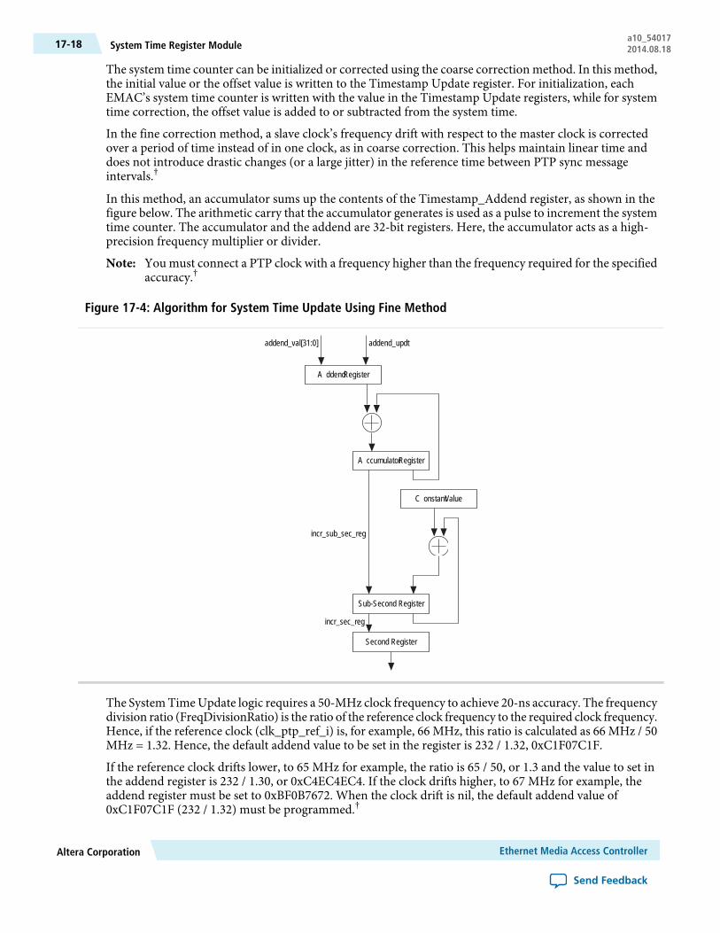
The system time counter can be initialized or corrected using the coarse correction method. In this method,the initial value or the offset value is written to the Timestamp Update register. For initialization, eachEMAC’s system time counter is written with the value in the Timestamp Update registers, while for systemtime correction, the offset value is added to or subtracted from the system time.
In the fine correction method, a slave clock’s frequency drift with respect to the master clock is correctedover a period of time instead of in one clock, as in coarse correction. This helps maintain linear time anddoes not introduce drastic changes (or a large jitter) in the reference time between PTP sync messageintervals.†
In this method, an accumulator sums up the contents of the Timestamp_Addend register, as shown in thefigure below. The arithmetic carry that the accumulator generates is used as a pulse to increment the systemtime counter. The accumulator and the addend are 32-bit registers. Here, the accumulator acts as a high-precision frequency multiplier or divider.
You must connect a PTP clock with a frequency higher than the frequency required for the specifiedaccuracy.†
Note:
Figure 17-4: Algorithm for System Time Update Using Fine Method
Addend Register
Accumulator Register
Constant Value
Sub-Second Register
Second Register
addend_val[31:0] addend_updt
incr_sub_sec_reg
incr_sec_reg
The System Time Update logic requires a 50-MHz clock frequency to achieve 20-ns accuracy. The frequencydivision ratio (FreqDivisionRatio) is the ratio of the reference clock frequency to the required clock frequency.Hence, if the reference clock (clk_ptp_ref_i) is, for example, 66 MHz, this ratio is calculated as 66 MHz / 50MHz = 1.32. Hence, the default addend value to be set in the register is 232 / 1.32, 0xC1F07C1F.
If the reference clock drifts lower, to 65 MHz for example, the ratio is 65 / 50, or 1.3 and the value to set inthe addend register is 232 / 1.30, or 0xC4EC4EC4. If the clock drifts higher, to 67 MHz for example, theaddend register must be set to 0xBF0B7672. When the clock drift is nil, the default addend value of0xC1F07C1F (232 / 1.32) must be programmed.†
Ethernet Media Access ControllerAltera Corporation
Send Feedback
a10_54017System Time Register Module17-18 2014.08.18

In the above figure, the constant value used to accumulate the sub-second register is decimal 43, whichachieves an accuracy of 20 ns in the system time (in other words, it is incremented in 20-ns steps).
The software must calculate the drift in frequency based on the Sync messages and update the Addendregister accordingly.†
Initially, the slave clock is set with FreqCompensationValue0 in theAddend register. This value is as follows:†
FreqCompensationValue0 = 232 / FreqDivisionRatio†
If MasterToSlaveDelay is initially assumed to be the same for consecutive sync messages, the algorithmdescribed below must be applied. After a few sync cycles, frequency lock occurs. The slave clock can thendetermine a precise MasterToSlaveDelay value and re-synchronize with the master using the new value.†
The algorithm is as follows:†
• At time MasterSyncTime n the master sends the slave clock a sync message. The slave receives thismessage when its local clock is SlaveClockTimen and computes MasterClockTimen as:†
MasterClockTimen = MasterSyncTimen + MasterToSlaveDelayn
†
• The master clock count for current sync cycle, MasterClockCountn is given by:†
MasterClockCountn = MasterClockTimen – MasterClockTimen-1 (assuming that MasterToSlaveDelay is the same for sync cycles n and n – 1)†
• The slave clock count for current sync cycle, SlaveClockCountn is given by:†
SlaveClockCountn = SlaveClockTimen – SlaveClockTimen-1
†
• The difference between master and slave clock counts for current sync cycle, ClockDiffCountn is givenby:†
ClockDiffCountn = MasterClockCountn – SlaveClockCountn
†
• The frequency-scaling factor for slave clock, FreqScaleFactorn is given by:†
FreqScaleFactorn = (MasterClockCountn + ClockDiffCountn) / SlaveClockCountn
†
• The frequency compensation value for Addend register, FreqCompensationValuen is given by: †
FreqCompensationValuen = FreqScaleFactorn × FreqCompensationValuen-1 – 1
†
In theory, this algorithm achieves lock in one Sync cycle; however, it may take several cycles, because ofchanging network propagation delays and operating conditions.†
This algorithm is self-correcting: if for any reason the slave clock is initially set to a value from the masterthat is incorrect, the algorithm corrects it at the cost of more Sync cycles.†
Altera CorporationEthernet Media Access Controller
Send Feedback
17-19System Time Register Modulea10_540172014.08.18

Transmit Path Functions
The MAC captures a timestamp when the SFD of a frame is sent on the PHY interface. The frames for whichyou want to capture timestamps are controllable on a per-frame basis. In other words, each transmit framecan be marked to indicate whether a timestamp should be captured for that frame. The MAC does notprocess the transmitted frames to identify the PTP frames. You need to specify the frames for which youwant to capture timestamps. The MAC returns the timestamp, along with the Transmit status of the frame,to hardware implemented in the FPGA. You can use the control bits in the transmit descriptor. The MACreturns the timestamp to the software inside the corresponding transmit descriptor, thus connecting thetimestamp automatically to the specific PTP frame.†
Receive Path Functions
The MAC captures the timestamp of all frames received on the PHY interface. The DMA returns thetimestamp to the software in the corresponding receive descriptor. The timestamp is written only to the lastreceive descriptor.†
Timestamp Error Margin
According to the IEEE 1588 specifications, a timestamp must be captured at the SFD of the transmitted andreceived frames at the PHY interface. Because the PHY interface receive and transmit clocks are notsynchronous to the reference timestamp clock (osc1_clk) a small amount of drift is introduced when atimestamp is moved between asynchronous clock domains. In the transmit path, the captured and reportedtimestamp has a maximum error margin of two PTP clocks. It means that the captured timestamp has thereference timing source value that is givenwithin two clocks after the SFD is transmitted on the PHY interface.
Similarly, in the receive path, the error margin is three PHY interface clocks, plus up to two PTP clocks. Youcan ignore the error margin because of the PHY interface clocks by assuming that this constant delay ispresent in the system (or link) before the SFD data reaches the PHY interface of the MAC.†
Frequency Range of Reference Timing Clock
The timestamp information is transferred across asynchronous clock domains, that is, from MAC clockdomain to the FPGA clock domain. Therefore, a minimum delay is required between two consecutivetimestamp captures. This delay is four clock cycles of the PHY interface and three clock cycles of PTP clocks.If the delay between two timestamp captures is less than this delay, the MAC does not take a timestampsnapshot for the second frame.
The maximum PTP clock frequency is limited by the maximum resolution of the reference time (20 nsresulting in 50MHz) and the timing constraints achievable for logic operating on the PTP clock. In addition,the resolution, or granularity, of the reference time source determines the accuracy of the synchronization.Therefore, a higher PTP clock frequency gives better system performance.†
The minimum PTP clock frequency depends on the time required between two consecutive SFD bytes.Because the PHY interface clock frequency is fixed by the IEEE 1588 specification, the minimum PTP clockfrequency required for proper operation depends upon the operating mode and operating speed of theMAC.†
Ethernet Media Access ControllerAltera Corporation
Send Feedback
a10_54017Transmit Path Functions17-20 2014.08.18

Table 17-6: Minimum PTP Clock Frequency Example
Minimum PTP FrequencyMinimum Gap Between Two SFDsMode
(3 * PTP) + (4 * MII) <= 168 * MII,that is, ~0.5 MHz (168 – 4) * 40 ns ÷3 = 2180 ns period)
168 MII clocks
(128 clocks for a 64-byte frame + 24clocks of min IFG + 16 clocks ofpreamble)
100-Mbps full-duplexoperation
(3 * PTP) + 4 * GMII <= 24 * GMII,that is, 18.75 MHz
24 GMII clocks
(4 for a jam pattern sent just after SFDbecause of collision + 12 IFG + 8preamble)
1000-Mbps half duplexoperation
Related InformationIEEE Standards Association websiteFor details about jam patterns, refer to the IEEE Std 802.3 2008 Part 3: Carrier sense multiple access withCollision Detection (CSMA/CD) Access Method and Physical Layer Specifications, available on the IEEEStandards Association website.
IEEE 1588-2008 Advanced TimestampsIn addition to the basic timestamp features mentioned in IEEE 1588-2002 Timestamps, the EMAC supportsthe following advanced timestamp features defined in the IEEE 1588-2008 standard.
†
• Supports the IEEE 1588-2008 (version 2) timestamp format. †
• Provides an option to take a timestamp of all frames or only PTP type frames. †
• Provides an option to take a timestamp of only event messages. †
• Provides an option to take the timestamp based on the clock type: ordinary, boundary, end-to-end, orpeer-to-peer. †
• Provides an option to configure the EMAC to be a master or slave for ordinary and boundary clock. †
• Identifies the PTP message type, version, and PTP payload in frames sent directly over Ethernet andsends the status. †
• Provides an option to measure sub-second time in digital or binary format. †
Related InformationIEEE Standards Association websiteFor more information about advanced timestamp features, refer to the IEEE Standard 1588 - 2008 IEEEStandard for a Precision Clock Synchronization Protocol for Networked Measurement and Control System,available on the IEEE Standards Association website.
Peer-to-Peer PTP Transparent Clock (P2P TC) Message Support
The IEEE 1588-2008 version supports Peer-to-Peer PTP (Pdelay) messages in addition to SYNC, DelayRequest, Follow-up, and Delay Response messages.†
Clock Types
The EMAC supports the following clock types defined in the IEEE 1588-2008 standard:
• Ordinary clock†
Altera CorporationEthernet Media Access Controller
Send Feedback
17-21IEEE 1588-2008 Advanced Timestampsa10_540172014.08.18

• Boundary clock†
• End-to-End transparent clock†
• Peer-to-Peer transparent clock†
Reference Timing Source
The EMAC supports the following reference timing source features defined in the IEEE 1588-2008 standard:
• 48-bit seconds Field†
• Fixed pulse-per-second output†
• Flexible pulse-per-second output†
• Auxiliary snapshots (timestamps) with external events
Transmit Path Functions
The advanced timestamp feature is supported through the descriptors format.
Receive Path Functions
The MAC processes the received frames to identify valid PTP frames. You can control the snapshot of thetime, to be sent to the application, by using the following options:†
• Enable timestamp for all frames.†
• Enable timestamp for IEEE 1588 version 2 or version 1 timestamp.†
• Enable timestamp for PTP frames transmitted directly over Ethernet or UDP/IP Ethernet.†
• Enable timestamp snapshot for the received frame for IPv4 or IPv6.†
• Enable timestamp snapshot for EVENT messages (SYNC, DELAY_REQ, PDELAY_REQ, orPDELAY_RESP) only.†
• Enable the node to be a master or slave and select the timestamp type. This controls the type of messagesfor which timestamps are taken.†
The DMA returns the timestamp to the software inside the corresponding transmit or receive descriptor.
Auxiliary Snapshot
The auxiliary snapshot feature allows you to store a snapshot (timestamp) of the system time based on anexternal event. The event is considered to be the rising edge of the sideband signal ptp_aux_ts_trig_i. Oneauxiliary snapshot input is available. The depth of the auxiliary snapshot FIFO buffer is 16.
The timestamps taken for any input are stored in a common FIFO buffer. The host can read a register toknow which input’s timestamp is available for reading at the top of this FIFO buffer. The MAC stores thesetimestamps in a FIFO buffer. Only 64 bits of the timestamp are stored in the FIFO buffer. When a timestampis stored, the MAC indicates this to the host with an interrupt. The value of the timestamp is read througha FIFO buffer register access. †
IEEE 802.3az Energy Efficient EthernetEnergy Efficient Ethernet (EEE) standardized by IEEE 802.3-az, version D2.0 is supported by the EMAC. Itis supported by the MAC operating in 10/100/1000 Mbps rates. EEE is only supported when the EMAC isconfigured to operate with the RGMII PHY interface operating in full-duplex mode. It does not supporthalf-duplex mode.
EEE enables the MAC to operate in Low-Power Idle (LPI) mode. Either end point of an Ethernet link candisable functionality to save power during periods of low link utilization. The MAC controls whether thesystem should enter or exit LPI mode and communicates this to the PHY.†
Ethernet Media Access ControllerAltera Corporation
Send Feedback
a10_54017Reference Timing Source17-22 2014.08.18
Related InformationIEEE 802.3az Energy Efficient EthernetFor details about the IEEE 802.3az Energy Efficient Ethernet standard, refer to the IEEE 802.3 EthernetWorking Group website.†
LPI Timers
Two timers internal to the EMAC are associated with LPI mode:
• LPI Link Status (LS) Timer†
• LPI TW Timer†
The LPI LS timer counts, in ms, the time expired since the link status is up. This timer is cleared every timethe link goes down and is incremented when the link is up again and the terminal count as programmed bythe software is reached. The PHY interface does not assert the LPI pattern unless the terminal count isreached. This ensures a minimum time for which no LPI pattern is asserted after a link is established withthe remote station. This period is defined as one second in the IEEE standard 802.3-az, version D2.0. TheLPI LS timer is 10 bits wide. Therefore, the software can program up to 1023 ms.†
The LPI TW timer counts, in µs, the time expired since the deassertion of LPI. The terminal count of thetimer is the value of resolved transmit TW that is the auto-negotiated time after which the MAC can resumethe normal transmit operation. The MAC supports the LPI TW timer in units of µs. The LPI TW timer is16 bits wide. Therefore, the software can program up to 65535 µs.†
The EMAC generates the LPI interrupt when the transmit or receive channel enters or exits the LPI state.†
Checksum OffloadCommunication protocols such as TCP and UDP implement checksum fields, which help determine theintegrity of data transmitted over a network. Because the most widespread use of Ethernet is to encapsulateTCP and UDP over IP datagrams, the EMAC has a Checksum Offload Engine (COE) to support checksumcalculation and insertion in the transmit path, and error detection in the receive path. Supported offloadingtypes:
• Transmit IP header checksum†
• Transmit TCP/UDP/ICMP checksum†
• Receive IP header checksum†
• Receive full checksum†
Frame FilteringThe EMAC implements the following types of filtering for receive frames.
Source Address or Destination Address Filtering
The Address Filtering Module checks the destination and source address field of each incoming packet.†
Unicast Destination Address Filter
Up to 128 MAC addresses for unicast perfect filtering are supported. The filter compares all 48 bits of thereceived unicast address with the programmed MAC address for any match. Default MacAddr0 is alwaysenabled, other addresses MacAddr1–MacAddr127 are selected with an individual enable bit. ForMacAddr1–MacAddr31 addresses, you can mask each byte during comparison with the correspondingreceived DA byte. This enables group address filtering for the DA. The MacAddr32-MacAddr127 addresses
Altera CorporationEthernet Media Access Controller
Send Feedback
17-23LPI Timersa10_540172014.08.18

do not have mask control and all six bytes of the MAC address are compared with the received six bytes ofDA.†
In hash filtering mode, the filter performs imperfect filtering for unicast addresses using a 256-bit hash table.It uses the upper ten bits of the CRC of the received destination address to index the content of the hashtable. A value of 0 selects Bit 0 of the selected register, and a value of 111111 binary selects Bit 63 of the HashTable register. If the corresponding bit is set to one, the unicast frame is said to have passed the hash filter;otherwise, the frame has failed the hash filter.†
Multicast Destination Address Filter
The MAC can be programmed to pass all multicast frames. In Perfect Filtering mode, the multicast addressis compared with the programmed MAC Destination Address registers (1–31). Group address filtering isalso supported. In hash filtering mode, the filter performs imperfect filtering using a 256-bit hash table. Forhash filtering, it uses the upper ten bits of the CRC of the received multicast address to index the contentsof the hash table. A value of 0 selects Bit 0 of the selected register and a value of 111111 binary selects Bit 63of the Hash Table register. If the corresponding bit is set to one, then the multicast frame is said to havepassed the hash filter; otherwise, the frame has failed the hash filter.†
Hash or Perfect Address Filter
The filter can be configured to pass a frame when its DA matches either the hash filter or the Perfect filter.This configuration applies to both unicast and multicast frames.†
Broadcast Address Filter
The filter does not filter any broadcast frames in the default mode. However, if the MAC is programmed toreject all broadcast frames, the filter drops any broadcast frame.†
Unicast Source Address Filter
TheMAC can also perform a perfect filtering based on the source address field of the received frames. Groupfiltering with SA is also supported. You can filter a group of addresses by masking one or more bytes of theaddress.†
Inverse Filtering Operation (Invert the Filter Match Result at Final Output)
For both Destination and Source address filtering, there is an option to invert the filter-match result at thefinal output. The result of the unicast or multicast destination address filter is inverted in this mode.†
VLAN Filtering
The EMAC supports the two kinds of VLAN filtering:
• VLAN tag-based filtering†
• VLAN hash filtering†
VLAN Tag-Based Filtering
In theVLAN tag-based frame filtering, theMAC compares theVLAN tag of the received frame and providesthe VLAN frame status to the application. Based on the programmed mode, the MAC compares the lower12 bits or all 16 bits of the receivedVLAN tag to determine the perfectmatch. If VLAN tag filtering is enabled,theMAC forwards theVLAN-tagged frames alongwithVLAN tagmatch status and drops theVLAN framesthat do not match. You can also enable the inverse matching for VLAN frames. In addition, you can enablematching of SVLAN tagged frames along with the default Customer Virtual Local Area Network (C-VLAN)tagged frames.†
Ethernet Media Access ControllerAltera Corporation
Send Feedback
a10_54017Multicast Destination Address Filter17-24 2014.08.18

VLAN Hash Filtering with a 16-Bit Hash Table
TheMACprovidesVLANhash filteringwith a 16-bit hash table. TheMACalso supports the inversematchingof the VLAN frames. In inverse matching mode, when the VLAN tag of a frame matches the perfect or hashfilter, the packet should be dropped. If the VLAN perfect and VLAN hash match are enabled, a frame isconsidered as matched if either the VLAN hash or the VLAN perfect filter matches. When inverse match isset, a packet is forwarded only when both perfect and hash filters indicate mismatch.†
Layer 3 and Layer 4 Filters
Layer 3 filtering refers to source address and destination address filtering. Layer 4 filtering refers to sourceport and destination port filtering. The frames are filtered in the following ways:†
• Matched frames†
• Unmatched frames†
• Non-TCP or UDP IP frames†
Matched Frames
The MAC forwards the frames, which match all enabled fields, to the application along with the status. TheMAC gives the matched field status only if one of the following conditions is true:†
• All enabled Layer 3 and Layer 4 fields match.†
• At least one of the enabled field matches and other fields are bypassed or disabled.†
Using the CSR set, you can define up to four filters, identified as filter 0 through filter 3. When multipleLayer 3 and Layer 4 filters are enabled, any filter match is considered as a match. If more than one filtermatches, the MAC provides status of the lowest filter with filter 0 being the lowest and filter 3 being thehighest. For example, if filter 0 and filter 1 match, the MAC gives the status corresponding to filter 0.†
Unmatched Frames
The MAC drops the frames that do not match any of the enabled fields. You can use the inverse matchfeature to block or drop a frame with specific TCP or UDP over IP fields and forward all other frames. Youcan configure the EMAC so that when a frame is dropped, it receives a partial frame with appropriate abortstatus or drops it completely.†
NonTCP or UDP IP Frames
By default, all non-TCP or UDP IP frames are bypassed from the Layer 3 and Layer 4 filters. You canoptionally program the MAC to drop all non-TCP or UDP over IP frames.†
Clocks and Resets
Clock Gating for EEE
For theRGMII PHY interface, you can gate the transmit clock for Energy Efficient Ethernet (EEE) applications.
Related InformationProgramming Guidelines for Energy Efficient Ethernet on page 17-58
Altera CorporationEthernet Media Access Controller
Send Feedback
17-25VLAN Hash Filtering with a 16-Bit Hash Tablea10_540172014.08.18
InterruptsInterrupts are generated as a result of specific events in the EMAC and external PHY device. The interruptstatus register indicates all conditions which may trigger an interrupt and the interrupt enable registerdetermines which interrupts can propagate.
Application Interface to FPGA FabricPending
Ethernet MAC Programming Model
DMA ControllerThe DMA has independent transmit and receive engines, and a CSR space. The transmit engine transfersdata from system memory to the device port or MAC transaction layer (MTL), while the receive enginetransfers data from the device port to the system memory. The controller use descriptors to efficiently movedata from source to destination with minimal Host CPU intervention. The DMA is designed for packet-oriented data transfers such as frames in Ethernet. The controller can be programmed to interrupt the HostCPU for situations such as frame transmit and receive transfer completion, and other normal/error conditions.
The DMA and the Host driver communicate through two data structures:†
• Control and Status registers (CSR)†
• Descriptor lists and data buffers †
Descriptor Lists and Data Buffers†
TheDMA transfers data frames received by theMAC to the receive Buffer in theHostmemory, and transmitdata frames from the transmit Buffer in the Host memory. Descriptors that reside in the Host memory actas pointers to these buffers.†
There are two descriptor lists: one for reception and one for transmission. The base address of each list iswritten into Register 3 (Receive Descriptor List Address Register) and Register 4 (Transmit Descriptor ListAddress Register), respectively. A descriptor list is forward linked (either implicitly or explicitly). The lastdescriptor may point back to the first entry to create a ring structure. Explicit chaining of descriptors isaccomplished by setting the second address chained in both receive and transmit descriptors (RDES1[24]and TDES1[24]). The descriptor lists resides in the Host physical memory address space. Each descriptorcan point to a maximum of two buffers. This enables two buffers to be used, physically addressed, ratherthan contiguous buffers in memory.†
A data buffer resides in the Host physical memory space, and consists of an entire frame or part of a frame,but cannot exceed a single frame. Buffers contain only data, buffer status is maintained in the descriptor.Data chaining refers to frames that span multiple data buffers. However, a single descriptor cannot spanmultiple frames. The DMA skips to the next frame buffer when end-of-frame is detected. Data chaining canbe enabled or disabled.†
Ethernet Media Access ControllerAltera Corporation
Send Feedback
a10_54017Interrupts17-26 2014.08.18

Figure 17-5: Descriptor Ring Structure
Descriptor 0Buffer 1
Buffer 1
Descriptor 0Buffer 1
Buffer 2
Descriptor 1Buffer 1
Buffer 2
Descriptor 2Buffer 1
Buffer 2
Descriptor nBuffer 1
Buffer 2
Figure 17-6: Descriptor Chain Structure
Descriptor 0Buffer 1
Descriptor 1 Buffer 1
Descriptor 2 Buffer 1
Next Descriptor
You can select a descriptor structure during RTL configuration. The control bits in the descriptorstructure are assigned so that the application can use an 8 KB buffer. All descriptions refer to thedefault descriptor structure.
Note:
Related Information
• DescriptorsDetailed bit map of the descriptor structure
• Ethernet MAC Address Map and Register DefinitionsInformation about Control and Status registers
Altera CorporationEthernet Media Access Controller
Send Feedback
17-27Descriptor Lists and Data Buffers†a10_540172014.08.18

Initialization for the EMAC
1. Write to Register 0 (Bus Mode Register) to set Host bus access parameters. †2. Write to Register 7 (Interrupt Enable Register) to mask unnecessary interrupt causes. †3. Create the transmit and receive descriptor lists, and then write to DMA Register 3 (Receive Descriptor
List Address Register) and Register 4 (Transmit Descriptor List Address Register), providing the DMAwith the starting address of each list. †
4. Write to Register 1 (MAC Frame Filter), Register 2 (Hash Table High Register), and Register 3 (HashTable Low Register) for desired filtering options. †
5. Write to Register 1 (MACFrame Filter) to configure the operatingmode and enable the transmit operation(Bit 3: Transmitter Enable). The PS and DM bits are set based on the auto-negotiation result (read fromthe PHY). †
6. Write to Register 6 (Operation Mode Register) to set Bits 13 and 1 to start transmission and reception. †7. Write toRegister 0 (MACConfigurationRegister) to enable the receive operation (Bit 2: Receiver Enable). †
The transmit and receive engines enter the Running state and attempt to acquire descriptors from therespective descriptor lists. The receive and transmit engines then begin processing receive and transmitoperations. The transmit and receive processes are independent of each other and can be started or stoppedseparately. †
Host Bus Burst Access
The DMA attempts to execute fixed-length Burst transfers on the master interface if configured to do sothrough FB bit of Register 0 (Bus Mode Register). The maximum Burst length is indicated and limited bythe PBL field (Bits [13:8]) Register 0 (Bus Mode Register). The receive and transmit descriptors are alwaysaccessed in the maximum possible (limited by PBL or 16 * 8/bus width) burst-size for the 16- bytes to beread.
The transmit DMA initiates a data transfer only when sufficient space to accommodate the configured burstis available in MTL transmit FIFO buffer or the number of bytes till the end of frame (when it is less thanthe configured burst-length). The DMA indicates the start address and the number of transfers required tothe master interface. When the interface is configured for fixed-length burst, then it transfers data using thebest combination of INCR4, 8, or 16 and SINGLE transactions. Otherwise (no fixed-length burst), it transfersdata using INCR (undefined length) and SINGLE transactions.
The receive DMA initiates a data transfer only when sufficient data to accommodate the configured burstis available in MTL receive FIFO buffer or when the end of frame (when it is less than the configured burst-length) is detected in the receive FIFO buffer. The DMA indicates the start address and the number oftransfers required to the master interface. When the interface is configured for fixed-length burst, then ittransfers data using the best combination of INCR4, 8, or 16 and SINGLE transactions. If the end-of frameis reached before the fixed-burst ends on the interface, then dummy transfers are performed in order tocomplete the fixed-burst. Otherwise (FB bit of Register 0 (Bus Mode Register) is reset), it transfers data usingINCR (undefined length) and SINGLE transactions.
When the interface is configured for address-aligned beats, both DMA engines ensure that the first bursttransfer initiated is less than or equal to the size of the configured PBL. Thus, all subsequent beats start atan address that is aligned to the configured PBL. The DMA can only align the address for beats up to size16 (for PBL > 16), because the interface does not support more than INCR16.
Host Data Buffer Alignment
The transmit and receive data buffers do not have any restrictions on start address alignment. For example,in systems with 32-bit memory, the start address for the buffers can be aligned to any of the four bytes.However, the DMA always initiates transfers with address aligned to the bus width with dummy data forthe byte lanes not required. This typically happens during the transfer of the beginning or end of an Ethernet
Ethernet Media Access ControllerAltera Corporation
Send Feedback
a10_54017Initialization for the EMAC17-28 2014.08.18

frame. The software driver should discard the dummy bytes based on the start address of the buffer and sizeof the frame.†
Example: Buffer Read
If the transmit buffer address is 0x00000FF2 (for 32-bit data bus), and 15 bytes need to be transferred, thenthe DMA reads five full words from address 0x00000FF0, but when transferring data to the MTL transmitFIFO buffer, the extra bytes (the first two bytes) are dropped or ignored. Similarly, the last 3 bytes of the lasttransfer are also ignored. The DMA always ensures it transfers a full 32-bit data to the MTL transmit FIFObuffer, unless it is the end-of-frame.
Example: Buffer Write
If the receive buffer address is 0x0000FF2 (for 64-bit data bus) and 16 bytes of a received frame need to betransferred, then the DMA writes 3 full words from address 0x00000FF0. But the first 2 bytes of first transferand the last 6 bytes of the third transfer have dummy data.
Buffer Size Calculations
The DMA does not update the size fields in the transmit and receive descriptors. The DMA updates onlythe status fields (RDES and TDES) of the descriptors. The driver has to perform the size calculations. †
The transmit DMA transfers the exact number of bytes (indicated by buffer size field of TDES1) towardsthe MAC. If a descriptor is marked as first (FS bit of TDES1 is set), then the DMA marks the first transferfrom the buffer as the start of frame. If a descriptor is marked as last (LS bit of TDES1), then the DMA marksthe last transfer from that data buffer as the end-of frame to the MTL. †
The receive DMA transfers data to a buffer until the buffer is full or the end-of frame is received from theMTL. If a descriptor is not marked as last (LS bit of RDES0), then the descriptor’s corresponding buffer(s)are full and the amount of valid data in a buffer is accurately indicated by its buffer size field minus the databuffer pointer offset when the FS bit of that descriptor is set. The offset is zero when the data buffer pointeris aligned to the data bus width. If a descriptor is marked as last, then the buffer may not be full (as indicatedby the buffer size in RDES1). To compute the amount of valid data in this final buffer, the driver must readthe frame length (FL bits of RDES0[29:16]) and subtract the sum of the buffer sizes of the preceding buffersin this frame. The receive DMA always transfers the start of next frame with a new descriptor. †
Even when the start address of a receive buffer is not aligned to the data width of system bus, thesystem should allocate a receive buffer of a size aligned to the system bus width. For example, if the
Note:
system allocates a 1,024-byte (1 KB) receive buffer starting from address 0x1000, the software canprogram the buffer start address in the receive descriptor to have a 0x1002 offset. The receive DMAwrites the frame to this buffer with dummy data in the first two locations (0x1000 and 0x1001). Theactual frame is written from location 0x1002. Thus, the actual useful space in this buffer is 1,022bytes, even though the buffer size is programmed as 1,024 bytes, because of the start address offset. †
Transmission
Transmission functions use transmit descriptors.
Related InformationTransmit Descriptor on page 17-40
TX DMA Operation: Default (Non-OSF) ModeThe transmit DMA engine in default mode proceeds as follows: †
1. The Host sets up the transmit descriptor (TDES0-TDES3) and sets the Own bit (TDES0[31]) after settingup the corresponding data buffer(s) with Ethernet frame data. †
Altera CorporationEthernet Media Access Controller
Send Feedback
17-29Example: Buffer Reada10_540172014.08.18

2. When Bit 13 (ST) of Register 6 (Operation Mode Register) is set, the DMA enters the Run state. †
3. While in the Run state, the DMA polls the transmit descriptor list for frames requiring transmission.After polling starts, it continues in either sequential descriptor ring order or chained order. If the DMAdetects a descriptor flagged as owned by the Host (TDES0[31] = 0), or if an error condition occurs,transmission is suspended and both the Bit 2 (Transmit Buffer Unavailable) and Bit 16 (Normal InterruptSummary) of the Register 5 (Status Register) are set. The transmit Engine proceeds to step 9.
4. If the acquired descriptor is flagged as owned by DMA (TDES0[31] = 1), the DMA decodes the transmitData Buffer address from the acquired descriptor.
5. The DMA fetches the transmit data from the Host memory and transfers the data to the MTL fortransmission. †
6. If an Ethernet frame is stored over data buffers in multiple descriptors, the DMA closes the intermediatedescriptor and fetches the next descriptor. Repeat step 3, step 4, and step 5 until the end-of-Ethernet-frame data is transferred to the MTL. †
7. When frame transmission is complete, if IEEE 1588 timestampingwas enabled for the frame (as indicatedin the transmit status) the timestamp value obtained from MTL is written to the transmit descriptor(TDES2 and TDES3) that contains the end-of-frame buffer. The status information is then written tothis transmit descriptor (TDES0). Because the Own bit is cleared during this step, the Host now ownsthis descriptor. If timestamping was not enabled for this frame, the DMA does not alter the contents ofTDES2 and TDES3. †
8. Bit 0 (Transmit Interrupt) of Register 5 (Status Register) is set after completing transmission of a framethat has Interrupt on Completion (TDES1[31]) set in its Last descriptor. The DMA engine then returnsto step 3. †
9. In the Suspend state, the DMA tries to re-acquire the descriptor (and thereby return to step 3) when itreceives a Transmit Poll demand and the Underflow Interrupt Status bit is cleared. †
Ethernet Media Access ControllerAltera Corporation
Send Feedback
a10_54017TX DMA Operation: Default (Non-OSF) Mode17-30 2014.08.18

Figure 17-7: TX DMA Operation in Default Mode
Error? yes
no
Own Bit Set?
yes
no
(Re-)Fetch NextDescriptor
StartTx DMA
Transfer Datafrom Buffer(s)
Error? yes
FrameTransferComplete?
yes
no
TimestampPresent?
yes
no
Write StatusWord to TDES0
Error?yesno
Write Timestampto RDES2 & RDES3
Error?yesno
StopTx DMA
Start
Tx DMASuspended
Poll Demand
Close IntermediateDescriptor
no
Wait forTx Status
Related InformationTX DMA Operation: Default (Non-OSF) Mode on page 17-29
Altera CorporationEthernet Media Access Controller
Send Feedback
17-31TX DMA Operation: Default (Non-OSF) Modea10_540172014.08.18
TX DMA Operation: OSF ModeWhile in the Run state, the transmit process can simultaneously acquire two frames without closing theStatus descriptor of the first [if Bit 2 (OSF) in Register 6 (Operation Mode Register) is set]. As the transmitprocess finishes transferring the first frame, it immediately polls the transmit descriptor list for the secondframe. If the second frame is valid, the transmit process transfers this frame before writing the first frame’sstatus information. †
In OSF mode, the Run state transmit DMA operates in the following sequence: †
1. The DMA operates as described in steps 1 - 6 of the TXDMAOperation: Default (Non-OSF)Mode onpage 17-29 section.
2. Without closing the previous frame’s last descriptor, the DMA fetches the next descriptor. †
3. If theDMAowns the acquired descriptor, theDMAdecodes the transmit buffer address in this descriptor.If the DMA does not own the descriptor, the DMA goes into Suspend mode and skips to step 7.†
4. The DMA fetches the transmit frame from the Host memory and transfers the frame to the MTL untilthe End-of-frame data is transferred, closing the intermediate descriptors if this frame is split acrossmultiple descriptors. †
5. The DMA waits for the previous frame’s frame transmission status and timestamp. Once the status isavailable, the DMA writes the timestamp to TDES2 and TDES3, if such timestamp was captured (asindicated by a status bit). The DMA then writes the status, with a cleared Own bit, to the correspondingTDES0, thus closing the descriptor. If timestamping was not enabled for the previous frame, the DMAdoes not alter the contents of TDES2 and TDES3. †
6. If enabled, the transmit interrupt is set, the DMA fetches the next descriptor, then proceeds to step 3(when Status is normal). If the previous transmission status shows an underflow error, the DMA goesinto Suspend mode ( step 7). †
7. In Suspend mode, if a pending status and timestamp are received from the MTL, the DMA writes thetimestamp (if enabled for the current frame) to TDES2 and TDES3, then writes the status to thecorresponding TDES0. It then sets relevant interrupts and returns to Suspend mode. †
8. The DMA can exit Suspend mode and enter the Run state (go to step 1 or step 2 depending on pendingstatus) only after receiving a Transmit Poll demand (Register 1 (Transmit Poll Demand Register). †
As the DMA fetches the next descriptor in advance before closing the currentdescriptor, the descriptor chain should have more than two different descriptors forcorrect and proper operation. †
Note:
Ethernet Media Access ControllerAltera Corporation
Send Feedback
a10_54017TX DMA Operation: OSF Mode17-32 2014.08.18

Figure 17-8: TX DMA Operation in OSF Mode
Error? yes
no
Own Bit Set?
yes
no
(Re-)Fetch NextDescriptor
StartTx DMA
Transfer Datafrom Buffer(s)
Error? yes
no
FrameTransferComplete?
no
TimestampPresent?
yes
no
Write Status Word toPrevious Frame’s TDES0
Error?no
yes
Write Timestampto TDES2 & TDES3for Previous Frame
Error?yesno
StopRx DMA
Start
TimestampPresent?
yes
no
Tx DMASuspended
Write Timestamp to RDES2 &TDES3 for Previous Frame
Poll Demand
yes
Wait for PreviousFrame’s TX Status
SecondFrame?
yes
no
Close IntermediateDescriptor
Error?
no
Error?no
Write Status Word toPrevious Frame’s TDES0
Previous FrameStatus Available
yes
yes
Altera CorporationEthernet Media Access Controller
Send Feedback
17-33TX DMA Operation: OSF Modea10_540172014.08.18

Transmit Frame Processing
The transmit DMA expects that the data buffers contain complete Ethernet frames, excluding preamble,pad bytes, and FCS fields. The DA, SA, and Type/Len fields contain valid data. If the transmit descriptorindicates that the MAC must disable CRC or PAD insertion, the buffer must have complete Ethernet frames(excluding preamble), including the CRC bytes. †
Frames can be data-chained and can span several buffers. Frames must be delimited by the First Descriptor(TDES1[29]) and the Last Descriptor (TDES1[30]), respectively. †
As transmission starts, the First Descriptormust have (TDES1[29]) set.When this occurs, frame data transfersfrom the Host buffer to the MTL transmit FIFO buffer. Concurrently, if the current frame has the LastDescriptor (TDES1[30]) clear, the transmit Process attempts to acquire the Next descriptor. The transmitProcess expects this descriptor to have TDES1[29] clear. If TDES1[30] is clear, it indicates an intermediarybuffer. If TDES1[30] is set, it indicates the last buffer of the frame. †
After the last buffer of the frame has been transmitted, the DMA writes back the final status information tothe TransmitDescriptor 0 (TDES0)word of the descriptor that has the last segment set in TransmitDescriptor1 (TDES1[30]). At this time, if Interrupt on Completion (TDES1[31]) is set, the Bit 0 (Transmit Interrupt)of Register 5 (Status Register) is set, the Next descriptor is fetched, and the process repeats. †
The actual frame transmission begins after theMTL transmit FIFObuffer has reached either a programmabletransmit threshold (Bits [16:14] of Register 6 (Operation Mode Register)), or a full frame is contained in theFIFO buffer. There is also an option for Store and Forward Mode (Bit 21 of Register 6 (Operation ModeRegister)). Descriptors are released (Own bit TDES0[31] clears) when the DMA finishes transferring theframe. †
To ensure proper transmission of a frame and the next frame, you must specify a non-zero buffersize for the transmit descriptor that has the Last Descriptor (TDES1[30]) set. †
Note:
Transmit Polling Suspended
Transmit polling can be suspended by either of the following conditions: †
• The DMA detects a descriptor owned by the Host (TDES0[31]=0). To resume, the driver must givedescriptor ownership to the DMA and then issue a Poll Demand command. †
• A frame transmission is aborted when a transmit error because of underflow is detected. The appropriateTransmit Descriptor 0 (TDES0) bit is set. †
If the DMA goes into SUSPEND state because of the first condition, then both Bit 16 (Normal InterruptSummary) and Bit 2 (Transmit Buffer Unavailable) of Register 5 (Status Register) are set. If the secondcondition occur, both Bit 15 (Abnormal Interrupt Summary) and Bit 5 (Transmit Underflow) of Register 5(Status Register) are set, and the information is written to Transmit Descriptor 0, causing the suspension. †
In both cases, the position in the transmit List is retained. The retained position is that of the descriptorfollowing the Last descriptor closed by the DMA. †
The driver must explicitly issue a Transmit Poll Demand command after rectifying the suspension cause. †
ReceptionReceive functions use receive descriptors.
The receive DMA engine’s reception sequence is depicted proceeds as follows:
1. The host sets up receive descriptors (RDES0-RDES3) and sets the Own bit (RDES0[31]).†
2. When Bit 1 (SR) of Register 6 (Operation Mode Register) is set, the DMA enters the Run state. While inthe Run state, the DMA polls the receive descriptor list, attempting to acquire free descriptors. If the
Ethernet Media Access ControllerAltera Corporation
Send Feedback
a10_54017Transmit Frame Processing17-34 2014.08.18

fetched descriptor is not free (is owned by the host), the DMA enters the Suspend state and jumps tostep 9.†
3. The DMA decodes the receive data buffer address from the acquired descriptors.†
4. Incoming frames are processed and placed in the acquired descriptor’s data buffers.†
5. When the buffer is full or the frame transfer is complete, the receive engine fetches the next descriptor.†
6. If the current frame transfer is complete, the DMA proceeds to step 7. If the DMA does not own thenext fetched descriptor and the frame transfer is not complete (EOF is not yet transferred), the DMAsets the Descriptor Error bit in the RDES0 (unless flushing is disabled in Bit 24 of Register 6 (OperationMode Register)). TheDMAcloses the current descriptor (clears theOwn bit) andmarks it as intermediateby clearing the Last Segment (LS) bit in the RDES0 value (marks it as Last Descriptor if flushing is notdisabled), then proceeds to step 8. If theDMAdoes own the next descriptor but the current frame transferis not complete, the DMA closes the current descriptor as intermediate and reverts to step 4.†
7. If IEEE 1588 timestamping is enabled, the DMA writes the timestamp (if available) to the currentdescriptor’s RDES2 and RDES3. It then takes the receive frame’s status from the MTL and writes thestatus word to the current descriptor’s RDES0, with the Own bit cleared and the Last Segment bit set.†
8. The receive engine checks the latest descriptor’s Own bit. If the host owns the descriptor (Own bit is 0),the Bit 7 (Receive Buffer Unavailable) of Register 5 (Status Register) is set and the DMA receive engineenters the Suspended state (Step 9). If the DMA owns the descriptor, the engine returns to step 4 andawaits the next frame.
9. Before the receive engine enters the Suspend state, partial frames are flushed from the receive FIFO buffer.You can control flushing using Bit 24 of Register 6 (Operation Mode Register). †
10. The receive DMA exits the Suspend state when a Receive Poll demand is given or the start of next frameis available from the MTL’s receive FIFO buffer. The engine proceeds to step 2 and refetches the nextdescriptor. †
Altera CorporationEthernet Media Access Controller
Send Feedback
17-35Receptiona10_540172014.08.18
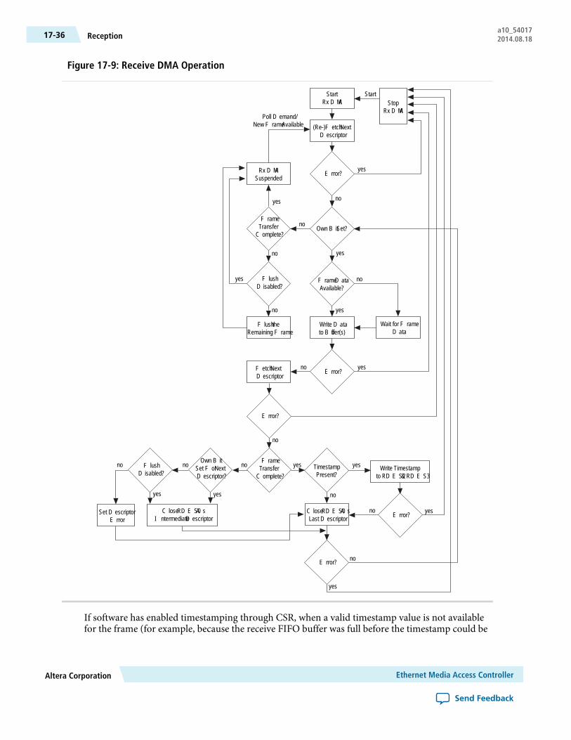
Figure 17-9: Receive DMA Operation
Error? yes
no
Own Bit Set?
yes
no
Frame DataAvailable?
no
yes
(Re-)Fetch NextDescriptor
StartRx DMA
Write Datato Buffer(s)
Error? yes
FrameTransferComplete?
yesno TimestampPresent?
yes
no
Close RDES0 AsLast Descriptor
Error? no
yes
Write Timestampto RDES2 & RDES3
Error? yesno
StopRx DMA
Start
Wait for FrameData
FrameTransferComplete?
yes
no
FlushDisabled?
no
Rx DMASuspended
Flush theRemaining Frame
yes
Poll Demand/New Frame Available
yes
noFlushDisabled?
yes
no
Close RDES0 AsIntermediate Descriptor
Set DescriptorError
Fetch NextDescriptor
Error?
no
Own BitSet For NextDescriptor?
no
If software has enabled timestamping through CSR, when a valid timestamp value is not availablefor the frame (for example, because the receive FIFO buffer was full before the timestamp could be
Ethernet Media Access ControllerAltera Corporation
Send Feedback
a10_54017Reception17-36 2014.08.18

written to it), the DMA writes all-ones to RDES2 and RDES3. Otherwise (that is, if timestampingis not enabled), the RDES2 and RDES3 remain unchanged. †
Related InformationReceive Descriptor
Receive Descriptor Acquisition
The receive Engine always attempts to acquire an extra descriptor in anticipation of an incoming frame.Descriptor acquisition is attempted if any of the following conditions is satisfied: †
• Bit 1 (Start or Stop Receive) of Register 6 (Operation Mode Register) has been set immediately after beingplaced in the Run state. †
• The data buffer of current descriptor is full before the frame ends for the current transfer. †• The controller has completed frame reception, but the current receive descriptor is not yet closed. †• The receive process has been suspended because of a host-owned buffer (RDES0[31] = 0) and a new
frame is received. †• A Receive poll demand has been issued. †
Receive Frame Processing
The MAC transfers the received frames to the Host memory only when the frame passes the address filterand frame size is greater than or equal to configurable threshold bytes set for the receive FIFO buffer ofMTL, or when the complete frame is written to the FIFO buffer in Store-and-Forward mode. †
If the frame fails the address filtering, it is dropped in the MAC block itself (unless Bit 31 (Receive All) ofRegister 1 (MACFrame Filter) is set). Frames that are shorter than 64 bytes, because of collision or prematuretermination, can be removed from the MTL receive FIFO buffer. †
After 64 (configurable threshold) bytes have been received, the MTL block requests the DMA block to begintransferring the frame data to the receive Buffer pointed by the current descriptor. The DMA sets FirstDescriptor (RDES0[9]) after the DMA Host interface becomes ready to receive a data transfer (if DMA isnot fetching transmit data from the host), to delimit the frame. The descriptors are released when the Own(RDES[31]) bit is reset to 0, either as the Data buffer fills up or as the last segment of the frame is transferredto the receive buffer. If the frame is contained in a single descriptor, both Last Descriptor (RDES[8]) andFirst Descriptor (RDES[9]) are set.
The DMA fetches the next descriptor, sets the Last Descriptor (RDES[8]) bit, and releases the RDES0 statusbits in the previous frame descriptor. Then the DMA sets the Bit 6 (Receive Interrupt) of Register 5 (StatusRegister). The same process repeats unless the DMA encounters a descriptor flagged as being owned by thehost. If this occurs, the receive Process sets the Bit 7 (Receive Buffer Unavailable) of Register 5 (StatusRegister) and then enters the Suspend state. The position in the receive list is retained. †
Receive Process Suspended
If a new receive frame arrives while the receive Process is in Suspend state, the DMA refetches the currentdescriptor in the Host memory. If the descriptor is now owned by the DMA, the receive Process re-entersthe Run state and starts frame reception. If the descriptor is still owned by the host, by default, the DMAdiscards the current frame at the top of the MTL RX FIFO buffer and increments the missed frame counter.If more than one frame is stored in the MTL EX FIFO buffer, the process repeats. †
The discarding or flushing of the frame at the top of the MTL EX FIFO buffer can be avoided by disablingFlushing (Bit 24 of Register 6 (Operation Mode Register)). In such conditions, the receive process sets theReceive Buffer Unavailable status and returns to the Suspend state. †
Altera CorporationEthernet Media Access Controller
Send Feedback
17-37Receive Descriptor Acquisitiona10_540172014.08.18
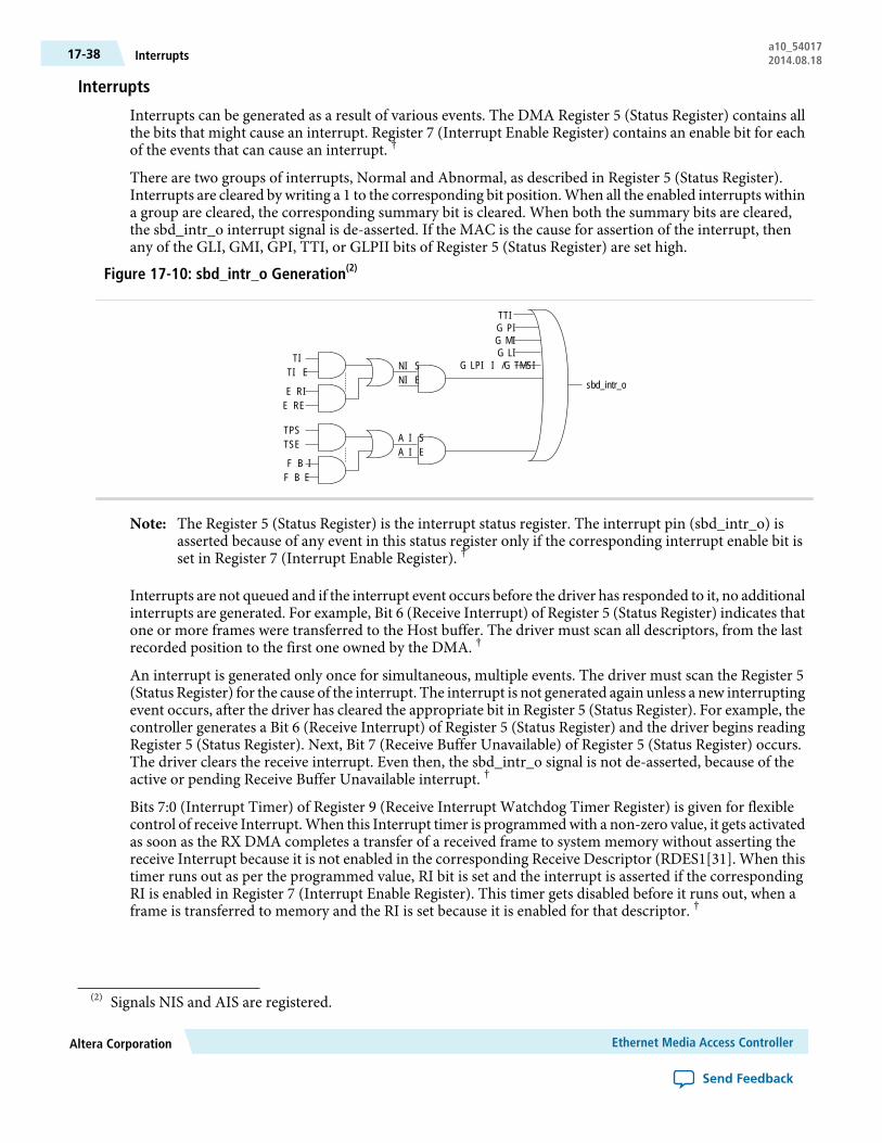
Interrupts
Interrupts can be generated as a result of various events. The DMA Register 5 (Status Register) contains allthe bits that might cause an interrupt. Register 7 (Interrupt Enable Register) contains an enable bit for eachof the events that can cause an interrupt. †
There are two groups of interrupts, Normal and Abnormal, as described in Register 5 (Status Register).Interrupts are cleared by writing a 1 to the corresponding bit position. When all the enabled interrupts withina group are cleared, the corresponding summary bit is cleared. When both the summary bits are cleared,the sbd_intr_o interrupt signal is de-asserted. If the MAC is the cause for assertion of the interrupt, thenany of the GLI, GMI, GPI, TTI, or GLPII bits of Register 5 (Status Register) are set high.
Figure 17-10: sbd_intr_o Generation(2)
sbd_intr_oERIERE
TITIE NIS
NIE
FBIFBE
TPSTSE AIS
AIE
TTIGPIGMIGLI
GLPII/GTMSI
The Register 5 (Status Register) is the interrupt status register. The interrupt pin (sbd_intr_o) isasserted because of any event in this status register only if the corresponding interrupt enable bit isset in Register 7 (Interrupt Enable Register). †
Note:
Interrupts are not queued and if the interrupt event occurs before the driver has responded to it, no additionalinterrupts are generated. For example, Bit 6 (Receive Interrupt) of Register 5 (Status Register) indicates thatone or more frames were transferred to the Host buffer. The driver must scan all descriptors, from the lastrecorded position to the first one owned by the DMA. †
An interrupt is generated only once for simultaneous, multiple events. The driver must scan the Register 5(Status Register) for the cause of the interrupt. The interrupt is not generated again unless a new interruptingevent occurs, after the driver has cleared the appropriate bit in Register 5 (Status Register). For example, thecontroller generates a Bit 6 (Receive Interrupt) of Register 5 (Status Register) and the driver begins readingRegister 5 (Status Register). Next, Bit 7 (Receive Buffer Unavailable) of Register 5 (Status Register) occurs.The driver clears the receive interrupt. Even then, the sbd_intr_o signal is not de-asserted, because of theactive or pending Receive Buffer Unavailable interrupt. †
Bits 7:0 (Interrupt Timer) of Register 9 (Receive Interrupt Watchdog Timer Register) is given for flexiblecontrol of receive Interrupt.When this Interrupt timer is programmedwith a non-zero value, it gets activatedas soon as the RX DMA completes a transfer of a received frame to system memory without asserting thereceive Interrupt because it is not enabled in the corresponding Receive Descriptor (RDES1[31]. When thistimer runs out as per the programmed value, RI bit is set and the interrupt is asserted if the correspondingRI is enabled in Register 7 (Interrupt Enable Register). This timer gets disabled before it runs out, when aframe is transferred to memory and the RI is set because it is enabled for that descriptor. †
(2) Signals NIS and AIS are registered.
Ethernet Media Access ControllerAltera Corporation
Send Feedback
a10_54017Interrupts17-38 2014.08.18
Related InformationReceive Descriptor on page 17-45
Error Response to DMA
For any data transfer initiated by a DMA channel, if the slave replies with an error response, that DMA stopsall operations and updates the error bits and the Fatal Bus Error bit in the Register 5 (Status Register). TheDMAcontroller can resume operation only after soft resetting or hard resetting the EMACand reinitializingthe DMA.
Descriptor OverviewThe DMA in the Ethernet subsystem transfers data based on a single descriptor, as explained inDMA Controller. The descriptor is created in the system memory. The descriptor addresses must be alignedto the used bus width (Word for 32-bit bus). The data bus is configured as little-endian.
The descriptor format can have 8 DWORDS (32 bytes). The descriptor contains two buffers, two byte-countbuffers, and two address pointers, which enable the adapter port to be compatible with various types ofmemory management schemes.
The features of the descriptor structure are:
• The descriptor structure is implemented to support buffers of up to 8 KB (useful for Jumbo frames).• There is a re-assignment of control and status bits in TDES0, TDES1, RDES0 (advanced timestamp or
IPC full offload configuration), and RDES1. †
• The transmit descriptor stores the timestamp in TDES6 and TDES7 when you select the advancedtimestamp. †
• This receive descriptor structure is also used for storing the extended status (RDES4) and timestamp(RDES6 and RDES7) when advanced timestamp, IPC Full Checksum Offload Engine, or Layer 3 andLayer 4 filter feature is selected. †
• You can select one of the following options for descriptor structure:
• If timestamping is enabled in Register 448 (Timestamp Control Register) or Checksum Offload isenabled in Register 0 (MAC Configuration Register), the software must to allocate 32 bytes (8DWORDS) of memory for every descriptor by setting Bit 7 (Descriptor Size) of Register 0 (Bus ModeRegister).
• If timestamping or Checksum Offload is not enabled, the extended descriptors (DES4 to DES7) arenot required. Therefore, software can use descriptors with the default size of 16 bytes (4 DWORDS)by clearing Bit 7 (Descriptor Size) of Register 0 (Bus Mode Register) to 0.
• When descriptor is selected without Timestamp or Receive IPC Full Checksum Offload Engine (Type 2)feature, the descriptor size is always 4DWORDs (DES0-DES3). Therefore, the software can use descriptorswith the default size of 16 bytes.
Related Information
• DMA Controller on page 17-26
• DescriptorsDetailed bit map of the descriptor structure
Altera CorporationEthernet Media Access Controller
Send Feedback
17-39Error Response to DMAa10_540172014.08.18

Transmit Descriptor
The application software must program the control bits TDES0[31:18] during the transmit descriptorinitialization. When the DMA updates the descriptor, it writes back all the control bits except the OWN bit(which it clears) and updates the status bits[7:0].
With the advance timestamp support, the snapshot of the timestamp to be taken can be enabled for a givenframe by setting Bit 25 (TTSE) of TDES0. When the descriptor is closed (that is, when the OWN bit iscleared), the timestamp is written into TDES6 and TDES7 as indicated by the status Bit 17 (TTSS) of TDES0.
When the advanced timestamp feature is enabled, software should set Bit 7 of Register 0 (Bus ModeRegister), so that the DMA operates with extended descriptor size. When this control bit is clear, theTDES4-TDES7 descriptor space is not valid. †
Note:
Figure 17-11: Transmit Descriptor Fields - Format
31 30 29 28 27 26 25 24 23 22 21 20 19 18 17 16 15 14 13 12 11 10 9 8 7 6 5 4 3 2 1 0
TDES0OWN
Ctrl [30:26]
TTSE
Ctrl [24:18]
TTSS
Status [16:7] Ctrl/Status[6:3]
Status[2:0]
TDES1 Ctrl[31:29] Buffer 2 Byte Count [28:16] RES Buffer 1 Byte Count [12:0]
]0:13[sserddA1reffuB2SEDT
]0:13[sserddArotpircseDtxeNro]0:13[sserddA2reffuB3SEDT
devreseR4SEDT
devreseR5SEDT
]0:13[woLpmatsemiTtimsnarT6SEDT
]0:13[hgiHpmatsemiTtimsnarT7SEDT
TheDMAalways reads or fetches fourDWORDS of the descriptor from systemmemory to obtain the bufferand control information. †
Ethernet Media Access ControllerAltera Corporation
Send Feedback
a10_54017Transmit Descriptor17-40 2014.08.18

Figure 17-12: Transmit Descriptor Fetch (Read) Format
31 30 29 28 27 26 25 24 23 22 21 20 19 18 17 16 15 14 13 12 11 10 9 8 7 6 5 4 3 2 1 0
TDES0OWN
Ctrl [30:26]
TTSE
Ctrl [24:18] Reserved for Status [17:7] SLOTNumber [6:3]
Reservedfor
Status[2:0]
TDES1 Ctrl[31:29] Buffer 2 Byte Count [28:16] RES Buffer 1 Byte Count [12:0]
]0:13[sserddA1reffuB2SEDT
]0:13[sserddArotpircseDtxeNro]0:13[sserddA2reffuB3SEDT
Table 17-7: Transmit Descriptor Word 0 (TDES0)
DescriptionBit
OWN: Own Bit
When set, this bit indicates that the descriptor is owned by the DMA. When this bit iscleared, it indicates that the descriptor is owned by the Host. The DMA clears this bit eitherwhen it completes the frame transmission or when the buffers allocated in the descriptorare read completely. The ownership bit of the frame’s first descriptor must be set after allsubsequent descriptors belonging to the same frame have been set to avoid a possible racecondition between fetching a descriptor and the driver setting an ownership bit. †
31
IC: Interrupt on Completion
When set, this bit sets the Transmit Interrupt (Register 5[0]) after the present frame hasbeen transmitted. †
30
LS: Last Segment
When set, this bit indicates that the buffer contains the last segment of the frame. Whenthis bit is set, the TBS1 or TBS2 field in TDES1 should have a non-zero value. †
29
FS: First Segment
When set, this bit indicates that the buffer contains the first segment of a frame. †
28
DC: Disable CRC
When this bit is set, the MAC does not append a CRC to the end of the transmitted frame.This bit is valid only when the first segment (TDES0[28]) is set. †
27
DP: Disable Pad
When set, the MAC does not automatically add padding to a frame shorter than 64 bytes.When this bit is cleared, the DMA automatically adds padding and CRC to a frame shorterthan 64 bytes, and the CRC field is added despite the state of the DC (TDES0[27]) bit. Thisbit is valid only when the first segment (TDES0[28]) is set. †
26
Altera CorporationEthernet Media Access Controller
Send Feedback
17-41Transmit Descriptora10_540172014.08.18

DescriptionBit
TTSE: Transmit Timestamp Enable
When set, this bit enables IEEE1588 hardware timestamping for the transmit framereferenced by the descriptor. This field is valid only when the First Segment control bit(TDES0[28]) is set.
25
Reserved24
CIC:Checksum InsertionControl. These bits control the checksumcalculation and insertion.The following list describes the bit encoding:
■ 0: Checksum insertion disabled.
■ 1: Only IP header checksum calculation and insertion are enabled.
■ 2: IP header checksum and payload checksum calculation and insertion are enabled, butpseudoheader checksum is not calculated in hardware.
■ 3: IP Header checksum and payload checksum calculation and insertion are enabled, andpseudoheader checksum is calculated in hardware.
This field is valid when the First Segment control bit (TDES0[28]) is set.
23:22
TER: Transmit End of Ring
When set, this bit indicates that the descriptor list reached its final descriptor. The DMAreturns to the base address of the list, creating a descriptor ring. †
21
TCH: Second Address Chained
When set, this bit indicates that the second address in the descriptor is the Next descriptoraddress rather than the second buffer address.WhenTDES0[20] is set, TBS2 (TDES1[28:16])is a “don’t care” value.
TDES0[21] takes precedence over TDES0[20]. †
20
Reserved19:18
TTSS: Transmit Timestamp Status
This field is used as a status bit to indicate that a timestamp was captured for the describedtransmit frame. When this bit is set, TDES2 and TDES3 have a timestamp value capturedfor the transmit frame. This field is only valid when the descriptor’s Last Segment controlbit (TDES0[29]) is set. †
17
IHE: IP Header Error
When set, this bit indicates that the MAC transmitter detected an error in the IP datagramheader. The transmitter checks the header length in the IPv4 packet against the number ofheader bytes received from the application and indicates an error status if there is amismatch. For IPv6 frames, a header error is reported if the main header length is not 40bytes. Furthermore, the Ethernet Length/Type field value for an IPv4 or IPv6 frame mustmatch the IPheader version received with the packet. For IPv4 frames, an error status isalso indicated if the Header Length field has a value less than 0x5. †
16
Ethernet Media Access ControllerAltera Corporation
Send Feedback
a10_54017Transmit Descriptor17-42 2014.08.18

DescriptionBit
ES: Error Summary
Indicates the logical OR of the following bits:
■ TDES0[14]: Jabber Timeout
■ TDES0[13]: Frame Flush
■ TDES0[11]: Loss of Carrier
■ TDES0[10]: No Carrier
■ TDES0[9]: Late Collision
■ TDES0[8]: Excessive Collision
■ TDES0[2]: Excessive Deferral
■ TDES0[1]: Underflow Error
■ TDES0[16]: IP Header Error
■ TDES0[12]: IP Payload Error †
15
JT: Jabber Timeout
When set, this bit indicates the MAC transmitter has experienced a jabber time-out. Thisbit is only set when Bit 22 (Jabber Disable) of Register 0 (MAC Configuration Register) isnot set. †
14
FF: Frame Flushed
When set, this bit indicates that the DMA or MTL flushed the frame because of a softwareFlush command given by the CPU. †
13
IPE: IP Payload Error
When set, this bit indicates that MAC transmitter detected an error in the TCP, UDP, orICMP IP datagram payload. The transmitter checks the payload length received in the IPv4or IPv6 header against the actual number of TCP, UDP, or ICMP packet bytes receivedfrom the application and issues an error status in case of a mismatch. †
12
LC: Loss of Carrier
When set, this bit indicates that a loss of carrier occurred during frame transmission (thatis, the gmii_crs_i signal was inactive for one or more transmit clock periods during frametransmission). This bit is valid only for the frames transmitted without collision when theMAC operates in the half-duplex mode. †
11
NC: No Carrier
When set, this bit indicates that the Carrier Sense signal form the PHY was not assertedduring transmission. †
10
Reserved9
Altera CorporationEthernet Media Access Controller
Send Feedback
17-43Transmit Descriptora10_540172014.08.18

DescriptionBit
EC: Excessive Collision
When set, this bit indicates that the transmission was aborted after 16 successive collisionswhile attempting to transmit the current frame. If Bit 9 (Disable Retry) bit in the Register0 (MAC Configuration Register) is set, this bit is set after the first collision, and thetransmission of the frame is aborted. †
8
VF: VLAN Frame
When set, this bit indicates that the transmitted frame is a VLAN-type frame. †
7
CC: Collision Count (Status field)
These status bits indicate the number of collisions that occurred before the frame wastransmitted. This count is not valid when the Excessive Collisions bit (TDES0[8]) is set.The EMAC updates this status field only in the half-duplex mode.
6:3
ED: Excessive Deferral
When set, this bit indicates that the transmission has ended because of excessive deferralof over 24,288 bit times (155,680 bits times in 1,000-Mbps mode or if Jumbo frame isenabled) if Bit 4 (Deferral Check) bit in Register 0 (MAC Configuration Register) is set. †
2
UF: Underflow Error
When set, this bit indicates that the MAC aborted the frame because the data arrived latefrom the Host memory. Underflow Error indicates that the DMA encountered an emptytransmit buffer while transmitting the frame. The transmission process enters the Suspendedstate and sets both Transmit Underflow (Register 5[5]) and Transmit Interrupt (Register5[0]). †
1
DB: Deferred Bit
When set, this bit indicates that theMACdefers before transmission because of the presenceof carrier. This bit is valid only in the half-duplex mode. †
0
Table 17-8: Transmit Descriptor Word 1 (TDES1)
DescriptionBit
Reserved31:29
TBS2: Transmit Buffer 2 Size
This field indicates the second data buffer size in bytes. This field is not valid if TDES0[20]is set. †
28:16
Reserved †15:13
TBS1: Transmit Buffer 1 Size
These bits indicate the first data buffer byte size, in bytes. If this field is 0, the DMA ignoresthis buffer and uses Buffer 2 or the next descriptor, depending on the value of TCH(TDES0[20]). †
12:0
Ethernet Media Access ControllerAltera Corporation
Send Feedback
a10_54017Transmit Descriptor17-44 2014.08.18
Table 17-9: Transmit Descriptor 2 (TDES2)
DescriptionBit
Buffer 1 Address Pointer
These bits indicate the physical address of Buffer 1. There is no limitation on the bufferaddress alignment. †
31:09
Table 17-10: Transmit Descriptor 3 (TDES3)
DescriptionBit
Buffer 2 Address Pointer (Next Descriptor Address)
Indicates the physical address of Buffer 2 when a descriptor ring structure is used. If theSecond Address Chained (TDES1[24]) bit is set, this address contains the pointer to thephysical memory where the Next descriptor is present. The buffer address pointer must bealigned to the bus width only when TDES1[24] is set. (LSBs are ignored internally.) †
31:09
Table 17-11: Transmit Descriptor 6 (TDES6)
DescriptionBit
TTSL: Transmit Frame Timestamp Low
This field is updated by DMA with the least significant 32 bits of the timestamp capturedfor the corresponding transmit frame. This field has the timestamp only if the Last Segmentbit (LS) in the descriptor is set and Timestamp status (TTSS) bit is set. †
31:09
Table 17-12: Transmit Descriptor 7 (TDES7)
DescriptionBit
TTSH: Transmit Frame Timestamp High
This field is updated by DMA with the most significant 32 bits of the timestamp capturedfor the corresponding receive frame. This field has the timestamp only if the Last Segmentbit (LS) in the descriptor is set and Timestamp status (TTSS) bit is set. †
31:09
Receive Descriptor
The receive descriptor can have 32 bytes of descriptor data (8 DWORDs) when advanced timestamp or IPCFull Offload feature is selected. When either of these features is enabled, software should set bit 7 of Register0 (Bus Mode Register) so that the DMA operates with extended descriptor size. When this control bit isclear, the RDES0[0] is always cleared and the RDES4-RDES7 descriptor space is not valid. †
Altera CorporationEthernet Media Access Controller
Send Feedback
17-45Receive Descriptora10_540172014.08.18
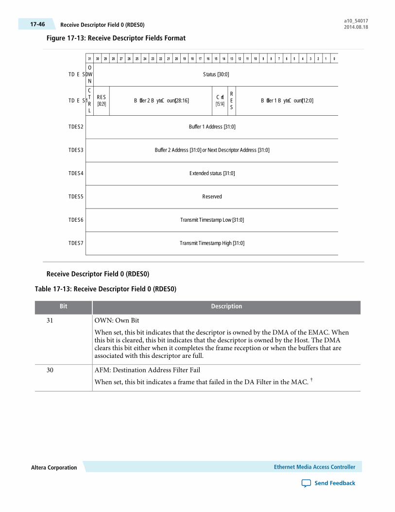
Figure 17-13: Receive Descriptor Fields Format
31 30 29 28 27 26 25 24 23 22 21 20 19 18 17 16 15 14 13 12 11 10 9 8 7 6 5 4 3 2 1 0
TDES0OWN
Status [30:0]
TDES1
CTRL
RES[30:29] Buffer 2 Byte Count [28:16] Ctrl
[15:14]
RES
Buffer 1 Byte Count [12:0]
]0:13[sserddA1reffuB2SEDT
]0:13[sserddArotpircseDtxeNro]0:13[sserddA2reffuB3SEDT
]0:13[sutatsdednetxE4SEDT
devreseR5SEDT
]0:13[woLpmatsemiTtimsnarT6SEDT
]0:13[hgiHpmatsemiTtimsnarT7SEDT
Receive Descriptor Field 0 (RDES0)
Table 17-13: Receive Descriptor Field 0 (RDES0)
DescriptionBit
OWN: Own Bit
When set, this bit indicates that the descriptor is owned by the DMA of the EMAC. Whenthis bit is cleared, this bit indicates that the descriptor is owned by the Host. The DMAclears this bit either when it completes the frame reception or when the buffers that areassociated with this descriptor are full.
31
AFM: Destination Address Filter Fail
When set, this bit indicates a frame that failed in the DA Filter in the MAC. †
30
Ethernet Media Access ControllerAltera Corporation
Send Feedback
a10_54017Receive Descriptor Field 0 (RDES0)17-46 2014.08.18

DescriptionBit
FL: Frame Length
These bits indicate the byte length of the received frame that was transferred to hostmemory(including CRC). This field is valid when Last Descriptor (RDES0[8]) is set and either theDescriptor Error (RDES0[14]) or Overflow Error bits are cleared. The frame length alsoincludes the two bytes appended to the Ethernet framewhen IP checksum calculation (Type1) is enabled and the received frame is not a MAC control frame.
This field is valid when Last Descriptor (RDES0[8]) is set. When the Last Descriptor andError Summary bits are not set, this field indicates the accumulated number of bytes thathave been transferred for the current frame. †
29:16
ES: Error Summary
Indicates the logical OR of the following bits:
• RDES0[1]: CRC Error• RDES0[3]: Receive Error• RDES0[4]: Watchdog Timeout• RDES0[6]: Late Collision• RDES0[7]: Giant Frame• RDES4[4:3]: IP Header or Payload Error (Receive Descriptor Field 4 (RDES4))• RDES0[11]: Overflow Error• RDES0[14]: Descriptor Error
This field is valid only when the Last Descriptor (RDES0[8]) is set. †
15
DE: Descriptor Error
When set, this bit indicates a frame truncation caused by a frame that does not fit withinthe current descriptor buffers, and that the DMA does not own the Next descriptor. Theframe is truncated. This bit is valid only when the Last Descriptor (RDES0[8]) is set. †
14
SAF: Source Address Filter Fail
When set, this bit indicates that the SA field of frame failed the SA Filter in the MAC. †
13
LE: Length Error
When set, this bit indicates that the actual length of the frame received and that the Length/Type field does not match. This bit is valid only when the Frame Type (RDES0[5]) bit isreset. †
12
OE: Overflow Error
When set, this bit indicates that the received framewas damaged because of buffer overflowin MTL.
Note: This bit is set only when the DMA transfers a partial frame to the application, whichhappens only when the RX FIFO buffer is operating in the threshold mode. In the store-and-forward mode, all partial frames are dropped completely in the RX FIFO buffer. †
11
Altera CorporationEthernet Media Access Controller
Send Feedback
17-47Receive Descriptor Field 0 (RDES0)a10_540172014.08.18
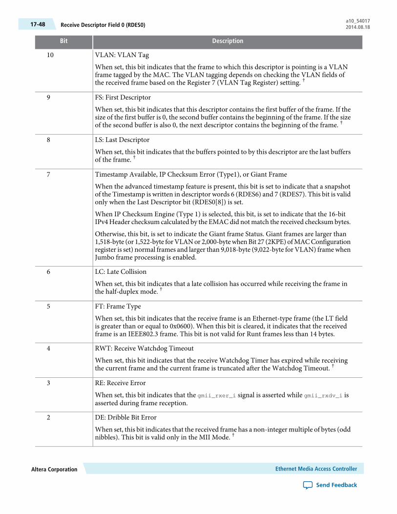
DescriptionBit
VLAN: VLAN Tag
When set, this bit indicates that the frame to which this descriptor is pointing is a VLANframe tagged by the MAC. The VLAN tagging depends on checking the VLAN fields ofthe received frame based on the Register 7 (VLAN Tag Register) setting. †
10
FS: First Descriptor
When set, this bit indicates that this descriptor contains the first buffer of the frame. If thesize of the first buffer is 0, the second buffer contains the beginning of the frame. If the sizeof the second buffer is also 0, the next descriptor contains the beginning of the frame. †
9
LS: Last Descriptor
When set, this bit indicates that the buffers pointed to by this descriptor are the last buffersof the frame. †
8
Timestamp Available, IP Checksum Error (Type1), or Giant Frame
When the advanced timestamp feature is present, this bit is set to indicate that a snapshotof the Timestamp is written in descriptor words 6 (RDES6) and 7 (RDES7). This bit is validonly when the Last Descriptor bit (RDES0[8]) is set.
When IP Checksum Engine (Type 1) is selected, this bit, is set to indicate that the 16-bitIPv4Header checksum calculated by the EMACdid notmatch the received checksumbytes.
Otherwise, this bit, is set to indicate the Giant frame Status. Giant frames are larger than1,518-byte (or 1,522-byte forVLANor 2,000-bytewhenBit 27 (2KPE) ofMACConfigurationregister is set) normal frames and larger than 9,018-byte (9,022-byte for VLAN) framewhenJumbo frame processing is enabled.
7
LC: Late Collision
When set, this bit indicates that a late collision has occurred while receiving the frame inthe half-duplex mode. †
6
FT: Frame Type
When set, this bit indicates that the receive frame is an Ethernet-type frame (the LT fieldis greater than or equal to 0x0600). When this bit is cleared, it indicates that the receivedframe is an IEEE802.3 frame. This bit is not valid for Runt frames less than 14 bytes.
5
RWT: Receive Watchdog Timeout
When set, this bit indicates that the receive Watchdog Timer has expired while receivingthe current frame and the current frame is truncated after the Watchdog Timeout. †
4
RE: Receive Error
When set, this bit indicates that the gmii_rxer_i signal is asserted while gmii_rxdv_i isasserted during frame reception.
3
DE: Dribble Bit Error
When set, this bit indicates that the received frame has a non-integer multiple of bytes (oddnibbles). This bit is valid only in the MII Mode. †
2
Ethernet Media Access ControllerAltera Corporation
Send Feedback
a10_54017Receive Descriptor Field 0 (RDES0)17-48 2014.08.18

DescriptionBit
CE: CRC Error
When set, this bit indicates that a CRC error occurred on the received frame. This bit isvalid only when the Last Descriptor (RDES0[8]) is set. †
1
Extended Status Available/RX MAC Address
When either advanced timestamp or IP Checksum Offload (Type 2) is present, this bit,when set, indicates that the extended status is available in descriptor word 4 (RDES4). Thisis valid only when the Last Descriptor bit (RDES0[8]) is set.
When Advance Timestamp Feature or IPC Full Offload is not selected, this bit indicatesRX MAC Address status. When set, this bit indicates that the RX MAC Address registersvalue (1 to 15) matched the frame’s DA field. When reset, this bit indicates that the RXMAC Address Register 0 value matched the DA field. †
0
Related Information
• Receive Descriptor Field 4 (RDES4) on page 17-51
• Receive Descriptor Field 6 (RDES6) on page 17-54
• Receive Descriptor Field 7 (RDES7) on page 17-54
Receive Descriptor Field 1 (RDES1)
Table 17-14: Receive Descriptor Field 1 (RDES1)
DescriptionBit
DIC: Disable Interrupt on Completion
When set, this bit prevents setting the Status Register’s RI bit (CSR5[6]) for the receivedframe ending in the buffer indicated by this descriptor. As a result, the RI interrupt for theframe is disabled and is not asserted to the Host.†
31
Reserved †30:29
RBS2: Receive Buffer 2 Size
These bits indicate the second data buffer size, in bytes. The buffer size must be a multipleof 4, even if the value of RDES3 (buffer2 address pointer) in Receive Descriptor Field 3(RDES3) is not aligned to bus width. If the buffer size is not an appropriate multiple of 4,the resulting behavior is undefined. This field is not valid if RDES1[14] is set. For moreinformation about calculating buffer sizes, refer to the Buffer Size Calculations section inthis chapter.
28:16
RER: Receive End of Ring
When set, this bit indicates that the descriptor list reached its final descriptor. The DMAreturns to the base address of the list, creating a descriptor ring. †
15
Altera CorporationEthernet Media Access Controller
Send Feedback
17-49Receive Descriptor Field 1 (RDES1)a10_540172014.08.18
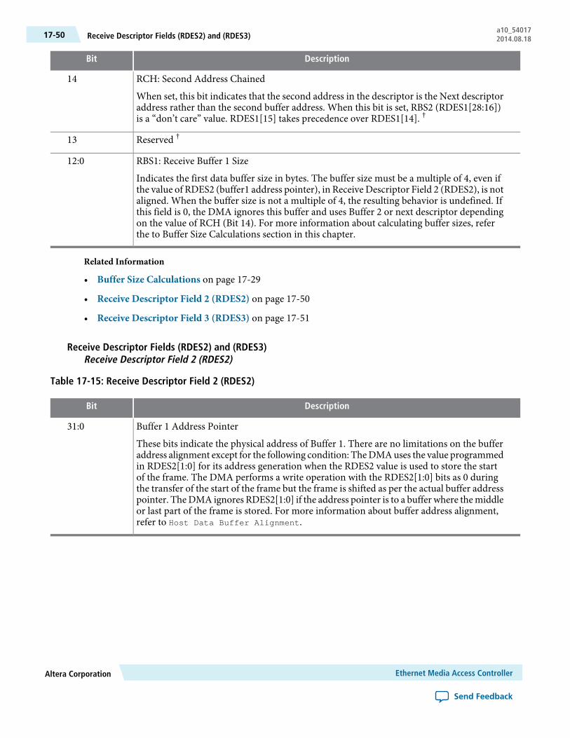
DescriptionBit
RCH: Second Address Chained
When set, this bit indicates that the second address in the descriptor is the Next descriptoraddress rather than the second buffer address. When this bit is set, RBS2 (RDES1[28:16])is a “don’t care” value. RDES1[15] takes precedence over RDES1[14]. †
14
Reserved †13
RBS1: Receive Buffer 1 Size
Indicates the first data buffer size in bytes. The buffer size must be a multiple of 4, even ifthe value of RDES2 (buffer1 address pointer), in Receive Descriptor Field 2 (RDES2), is notaligned. When the buffer size is not a multiple of 4, the resulting behavior is undefined. Ifthis field is 0, the DMA ignores this buffer and uses Buffer 2 or next descriptor dependingon the value of RCH (Bit 14). For more information about calculating buffer sizes, referthe to Buffer Size Calculations section in this chapter.
12:0
Related Information
• Buffer Size Calculations on page 17-29
• Receive Descriptor Field 2 (RDES2) on page 17-50
• Receive Descriptor Field 3 (RDES3) on page 17-51
Receive Descriptor Fields (RDES2) and (RDES3)Receive Descriptor Field 2 (RDES2)
Table 17-15: Receive Descriptor Field 2 (RDES2)
DescriptionBit
Buffer 1 Address Pointer
These bits indicate the physical address of Buffer 1. There are no limitations on the bufferaddress alignment except for the following condition: TheDMAuses the value programmedin RDES2[1:0] for its address generation when the RDES2 value is used to store the startof the frame. The DMA performs a write operation with the RDES2[1:0] bits as 0 duringthe transfer of the start of the frame but the frame is shifted as per the actual buffer addresspointer. The DMA ignores RDES2[1:0] if the address pointer is to a buffer where the middleor last part of the frame is stored. For more information about buffer address alignment,refer to Host Data Buffer Alignment.
31:0
Ethernet Media Access ControllerAltera Corporation
Send Feedback
a10_54017Receive Descriptor Fields (RDES2) and (RDES3)17-50 2014.08.18
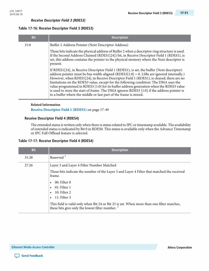
Receive Descriptor Field 3 (RDES3)
Table 17-16: Receive Descriptor Field 3 (RDES3)
DescriptionBit
Buffer 2 Address Pointer (Next Descriptor Address)
These bits indicate the physical address of Buffer 2 when a descriptor ring structure is used.If the Second Address Chained (RDES1[24]) bit, in Receive Descriptor Field 1 (RDES1), isset, this address contains the pointer to the physical memory where the Next descriptor ispresent.
If RDES1[24], in Receive Descriptor Field 1 (RDES1), is set, the buffer (Next descriptor)address pointer must be bus width-aligned (RDES3[1:0] = 0. LSBs are ignored internally.)However, when RDES1[24], in Receive Descriptor Field 1 (RDES1), is cleared, there are nolimitations on the RDES3 value, except for the following condition: The DMA uses thevalue programmed in RDES3 [1:0] for its buffer address generation when the RDES3 valueis used to store the start of frame. The DMA ignores RDES3 [1:0] if the address pointer isto a buffer where the middle or last part of the frame is stored.
31:0
Related InformationReceive Descriptor Field 1 (RDES1) on page 17-49
Receive Descriptor Field 4 (RDES4)
The extended status is written only when there is status related to IPC or timestamp available. The availabilityof extended status is indicated by Bit 0 in RDES0. This status is available only when the Advance Timestampor IPC Full Offload feature is selected.
Table 17-17: Receive Descriptor Field 4 (RDES4)
DescriptionBit
Reserved †31:28
Layer 3 and Layer 4 Filter Number Matched
These bits indicate the number of the Layer 3 and Layer 4 Filter that matched the receivedframe.
• 00: Filter 0• 01: Filter 1• 10: Filter 2• 11: Filter 3
This field is valid only when Bit 24 or Bit 25 is set. When more than one filter matches,these bits give only the lowest filter number. †
27:26
Altera CorporationEthernet Media Access Controller
Send Feedback
17-51Receive Descriptor Field 3 (RDES3)a10_540172014.08.18
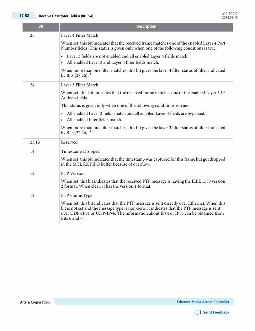
DescriptionBit
Layer 4 Filter Match
When set, this bit indicates that the received frame matches one of the enabled Layer 4 PortNumber fields. This status is given only when one of the following conditions is true:
• Layer 3 fields are not enabled and all enabled Layer 4 fields match.• All enabled Layer 3 and Layer 4 filter fields match.
When more than one filter matches, this bit gives the layer 4 filter status of filter indicatedby Bits [27:26]. †
25
Layer 3 Filter Match
When set, this bit indicates that the received frame matches one of the enabled Layer 3 IPAddress fields.
This status is given only when one of the following conditions is true:
• All enabled Layer 3 fields match and all enabled Layer 4 fields are bypassed.• All enabled filter fields match.
When more than one filter matches, this bit gives the layer 3 filter status of filter indicatedby Bits [27:26]. †
24
Reserved23:15
Timestamp Dropped
When set, this bit indicates that the timestamp was captured for this frame but got droppedin the MTL RX FIFO buffer because of overflow.
14
PTP Version
When set, this bit indicates that the received PTP message is having the IEEE 1588 version2 format. When clear, it has the version 1 format.
13
PTP Frame Type
When set, this bit indicates that the PTP message is sent directly over Ethernet. When thisbit is not set and the message type is non-zero, it indicates that the PTP message is sentover UDP-IPv4 or UDP-IPv6. The information about IPv4 or IPv6 can be obtained fromBits 6 and 7.
12
Ethernet Media Access ControllerAltera Corporation
Send Feedback
a10_54017Receive Descriptor Field 4 (RDES4)17-52 2014.08.18

DescriptionBit
Message Type
These bits are encoded to give the type of the message received.
• 0000: No PTP message received• 0001: SYNC (all clock types)• 0010: Follow_Up (all clock types)• 0011: Delay_Req (all clock types)• 0100: Delay_Resp (all clock types)• 0101: Pdelay_Req (in peer-to-peer transparent clock)• 0110: Pdelay_Resp (in peer-to-peer transparent clock)• 0111: Pdelay_Resp_Follow_Up (in peer-to-peer transparent clock)• 1000: Announce• 1001: Management• 1010: Signaling• 1011-1110: Reserved• 1111: PTP packet with Reserved message type
11:8
IPv6 Packet Received
When set, this bit indicates that the received packet is an IPv6 packet. This bit is updatedonly when Bit 10 (IPC) of Register 0 (MAC Configuration Register) is set.
7
IPv4 Packet Received
When set, this bit indicates that the received packet is an IPv4 packet. This bit is updatedonly when Bit 10 (IPC) of Register 0 (MAC Configuration Register) is set.
6
IP Checksum Bypassed
When set, this bit indicates that the checksum offload engine is bypassed.
5
IP Payload Error
When set, this bit indicates that the 16-bit IP payload checksum (that is, the TCP, UDP, orICMP checksum) that the EMAC calculated does not match the corresponding checksumfield in the received segment. It is also set when the TCP, UDP, or ICMP segment lengthdoes not match the payload length value in the IP Header field. This bit is valid when eitherBit 7 or Bit 6 is set.
4
IP Header Error
When set, this bit indicates that either the 16-bit IPv4 header checksum calculated by theEMAC does not match the received checksum bytes, or the IP datagram version is notconsistent with the Ethernet Type value. This bit is valid when either Bit 7 or Bit 6 is set.
3
Altera CorporationEthernet Media Access Controller
Send Feedback
17-53Receive Descriptor Field 4 (RDES4)a10_540172014.08.18

DescriptionBit
IP Payload Type
These bits indicate the type of payload encapsulated in the IP datagram processed by thereceive Checksum Offload Engine (COE). The COE also sets these bits to 0 if it does notprocess the IP datagram’s payload due to an IP header error or fragmented IP.
• 0: Unknown or did not process IP payload• 1: UDP• 2: TCP• 3: ICMP• 4–7: Reserved
This bit is valid when either Bit 7 or Bit 6 is set.
2:0
Related InformationReceive Descriptor Field 0 (RDES0) on page 17-46
Receive Descriptor Fields (RDES6) and (RDES7)
ReceiveDescriptor Fields 6 and 7 (RDES6 andRDES7) contain the snapshot of the timestamp. The availabilityof the snapshot of the timestamp in RDES6 and RDES7 is indicated by Bit 7 in the RDES0 descriptor.
Related InformationReceive Descriptor Field 0 (RDES0) on page 17-46
Receive Descriptor Field 6 (RDES6)
Table 17-18: Receive Descriptor Field 6 (RDES6)
DescriptionBit
RTSL: Receive Frame Timestamp Low
This field is updated by DMA with the least significant 32 bits of the timestamp capturedfor the corresponding receive frame. This field is updated byDMAonly for the last descriptorof the receive frame, which is indicated by Last Descriptor status bit (RDES0[8]) in RDES0.
31:0
Related InformationReceive Descriptor Field 0 (RDES0) on page 17-46
Receive Descriptor Field 7 (RDES7)
Table 17-19: Receive Descriptor Field 7 (RDES7)
DescriptionBit
RTSH: Receive Frame Timestamp High
This field is updated by DMA with the most significant 32 bits of the timestamp capturedfor the corresponding receive frame. This field is updated byDMAonly for the last descriptorof the receive frame, which is indicated by Last Descriptor status bit (RDES0[8]) in RDES0.
31:0
Ethernet Media Access ControllerAltera Corporation
Send Feedback
a10_54017Receive Descriptor Fields (RDES6) and (RDES7)17-54 2014.08.18

Related InformationReceive Descriptor Field 0 (RDES0) on page 17-46
Initializing DMAThis section provides the instructions for initializing the DMA/MAC registers in the proper sequence.Perform the following steps to initialize the DMA:
1. Provide a software reset to reset all of the EMAC internal registers and logic. (DMA Register 0 (Bus ModeRegister) – bit 0). †
2. Wait for the completion of the reset process (poll bit 0 of the DMA Register 0 (Bus Mode Register), whichis only cleared after the reset operation is completed). †
3. Poll the bits of Register 11 (AHB or AXI Status) to confirm that all previously initiated (before software-reset) or ongoing transactions are complete.
If the application cannot poll the register after soft reset (because of performance reasons), thenit is recommended that you continuewith the next steps and check this register again (asmentionedin 12 on page 17-56) before triggering the DMA operations.†
Note:
4. Program the following fields to initialize the Bus Mode Register by setting values in DMA Register 0 (BusMode Register):†
• Mixed Burst and AAL• Fixed burst or undefined burst†
• Burst length values and burst mode values†
• Descriptor Length (only valid if Ring Mode is used)†
• TX and RX DMA Arbitration scheme†
5. Program the interface options in Register 10 (AXI Bus Mode Register). If fixed burst-length is enabled,then select the maximum burst-length possible on the bus (bits[7:1]).†
6. Create a proper descriptor chain for transmit and receive. In addition, ensure that the receive descriptorsare owned by DMA (bit 31 of descriptor should be set). When OSF mode is used, at least two descriptorsare required.
7. Make sure that your software creates three or more different transmit or receive descriptors in the chainbefore reusing any of the descriptors.†
8. Initialize receive and transmit descriptor list address with the base address of the transmit and receivedescriptor (Register 3 (Receive Descriptor List Address Register) and Register 4 (Transmit DescriptorList Address Register) respectively).†
9. Program the following fields to initialize the mode of operation in Register 6 (Operation Mode Register):
• Receive and Transmit Store And Forward†
• Receive and Transmit Threshold Control (RTC and TTC)†
• Hardware Flow Control enable†
• Flow Control Activation and De-activation thresholds for MTL Receive and Transmit FIFO buffers(RFA and RFD)†
• Error frame and undersized good frame forwarding enable†
• OSF Mode†
10. Clear the interrupt requests, by writing to those bits of the status register (interrupt bits only) that areset. For example, by writing 1 into bit 16, the normal interrupt summary clears this bit (DMA Register5 (Status Register)).†
11. Enable the interrupts by programming the Register 7 (Interrupt Enable Register).†
Altera CorporationEthernet Media Access Controller
Send Feedback
17-55Initializing DMAa10_540172014.08.18

Note: Perform 12 on page 17-56 only if you did not perform 3 on page 17-55.†
12. Read Register 11 (AHB or AXI Status) to confirm that all previous transactions are complete.†
If any previous transaction is still in progress when you read the Register 11 (AHB or AXI Status),then it is strongly recommended to check the slave components addressed by themaster interface.†
Note:
13. Start the receive and transmit DMA by setting SR (bit 1) and ST (bit 13) of the control register (DMARegister 6 (Operation Mode Register). †
Related InformationDescriptorsDetailed bit map of the descriptor structure
Initializing MACThe following MAC Initialization operations can be performed after DMA initialization. If the MACinitialization is done before the DMA is set up, then enable the MAC receiver (last step below) only afterthe DMA is active. Otherwise, received frames fill the RX FIFO buffer and overflow.
1. Program the EMAC Register 4 (GMII Address Register) for controlling the management cycles for theexternal PHY. For example, Physical Layer Address PA (bits 15-11). In addition, set bit 0 (GMII Busy)for writing into the PHY and reading from the PHY. †
2. Read the 16-bit data of Register 5 (GMII Data Register) from the PHY for link up, speed of operation,and mode of operation, by specifying the appropriate address value in bits 15-11 of Register 4 (GMIIAddress Register). †
3. Provide the MAC address registers (Register 16 (MAC Address0 High Register) and Register 17 (MACAddress0 Low Register)). Because 128 MAC addresses are supported, you must program the MACaddresses accordingly.
4. Program Register 2 (Hash Table High Register) and Register 3 (Hash Table Low Register).5. Program the following fields to set the appropriate filters for the incoming frames in Register 1 (MAC
Frame Filter): †
• Receive All †• Promiscuous mode †• Hash or Perfect Filter †• Unicast, multicast, broadcast, and control frames filter settings †
6. Program the following fields for proper flow control in Register 6 (Flow Control Register): †
• Pause time and other pause frame control bits †• Receive and Transmit Flow control bits †• Flow Control Busy/Backpressure Activate †
7. Program the Interrupt Mask register bits, as required, and if applicable, for your configuration. †8. Program the appropriate fields in Register 0 (MAC Configuration Register). For example, Interframe
gap while transmission and jabber disable. Based on the Auto-negotiation you can set the Duplex mode(bit 11) or port select (bit 15). †
9. Set Bit 3 (TE) and Bit 2 (RE) in Register 0 (MAC Configuration Register). †
Ethernet Media Access ControllerAltera Corporation
Send Feedback
a10_54017Initializing MAC17-56 2014.08.18

Do not change the configuration (such as duplex mode, speed, port, or loopback) when the EMACDMA is actively transmitting or receiving. Software should change these parameters only when theEMAC DMA transmitter and receiver are not active.
Note:
Performing Normal Receive and Transmit OperationFor normal operation, perform the following steps: †
1. For normal transmit and receive interrupts, read the interrupt status. Then, poll the descriptors, readingthe status of the descriptor owned by the Host (either transmit or receive). †
2. Set appropriate values for the descriptors, ensuring that transmit and receive descriptors are owned bythe DMA to resume the transmission and reception of data. †
3. If the descriptors are not owned by theDMA (or no descriptor is available), theDMAgoes into SUSPENDstate. The transmission or reception can be resumed by freeing the descriptors and issuing a poll demandby writing 0 into the TX/RX poll demand register (Register 1 (Transmit Poll Demand Register) andRegister 2 (Receive Poll Demand Register). †
4. The values of the current host transmitter or receiver descriptor address pointer can be read for the debugprocess (Register 18 (Current Host Transmit Descriptor Register) and Register 19 (Current Host ReceiveDescriptor Register). †
5. The values of the current host transmit buffer address pointer and receive buffer address pointer can beread for the debug process (Register 20 (Current Host Transmit Buffer Address Register) and Register21 (Current Host Receive Buffer Address Register). †
Stopping and Starting TransmissionPerform the following steps to pause the transmission for some time: †
Altera CorporationEthernet Media Access Controller
Send Feedback
17-57Performing Normal Receive and Transmit Operationa10_540172014.08.18
1. Disable the transmit DMA (if applicable), by clearing bit 13 (Start or Stop Transmission Command) ofRegister 6 (Operation Mode Register). †
2. Wait for any previous frame transmissions to complete. You can check this by reading the appropriatebits of Register 9 (Debug Register). †
3. Disable the MAC transmitter and MAC receiver by clearing Bit 3 (TE) and Bit 2 (RE) in Register 0 (MACConfiguration Register). †
4. Disable the receiveDMA (if applicable), aftermaking sure that the data in the RXFIFObuffer is transferredto the system memory (by reading Register 9 (Debug Register). †
5. Make sure that both TX FIFO buffer and RX FIFO buffer are empty. †6. To re-start the operation, first start the DMAs, and then enable the MAC transmitter and receiver. †
Programming Guidelines for Energy Efficient Ethernet
Entering and Exiting the TX LPI Mode
The Energy Efficient Ethernet (EEE) feature is available in the EMAC. To use it, perform the following stepsduring EMAC initialization:
1. Read the PHY register through the MDIO interface, check if the remote end has the EEE capability, andthen negotiate the timer values. †
2. Program the PHY registers through the MDIO interface (including the RX_CLK_stoppable bit thatindicates to the PHY whether to stop RX clock in LPI mode.) †
3. Program Bits[16:5], LST, and Bits[15:0], TWT, in Register 13 (LPI Timers Control Register). †
4. Read the link status of the PHY chip by using the MDIO interface and update Bit 17 (PLS) of Register12 (LPI Control and Status Register) accordingly. This update should be done whenever the link statusin the PHY chip changes. †
5. Set Bit 16 (LPIEN) of Register 12 (LPI Control and Status Register) to make the MAC enter the LPI state.The MAC enters the LPI mode after completing the transmission in progress and sets Bit 0 (TLPIEN). †
Tomake theMACenter the LPI state only after it completes the transmission of all queued framesin the TX FIFO buffer, you should set Bit 19 (LPITXA) in Register 12 (LPI Control and StatusRegister). †
Note:
To switch off the transmit clock during the LPI state, use the sbd_tx_clk_gating_ctrl_o signalfor gating the clock input. †
Note:
To switch off the CSR clock or power to the rest of the system during the LPI state, you shouldwait for the TLPIEN interrupt of Register 12 (LPI Control and Status Register) to be generated.
Note:
Restore the clocks before performing the 6 on page 17-58 when you want to come out of the LPIstate. †
6. Clear Bit 16 (LPIEN) of Register 12 (LPI Control and Status Register) to bring the MAC out of the LPIstate. †
The MAC waits for the time programmed in Bits [15:0], TWT, before setting the TLPIEX interrupt statusbit and resuming the transmission. †
Gating Off the CSR Clock in the LPI Mode
You can gate off the CSR clock to save the power when the MAC is in the Low-Power Idle (LPI) mode.†
Ethernet Media Access ControllerAltera Corporation
Send Feedback
a10_54017Programming Guidelines for Energy Efficient Ethernet17-58 2014.08.18
Gating Off the CSR Clock in the RX LPI Mode
The following operations are performed when the MAC receives the LPI pattern from the PHY. †
1. The MAC RX enters the LPI mode and the RX LPI entry interrupt status [RLPIEN interrupt of Register12 (LPI_Control_Status)] is set. †
2. The interrupt pin (sbd_intr_o) is asserted. The sbd_intr_o interrupt is cleared when the host reads theRegister 12 (LPI_Control_Status). †
After the sbd_intr_o interrupt is asserted and the MAC TX is also in the LPI mode, you can gate off theCSR clock. If the MAC TX is not in the LPI mode when you gate off the CSR clock, the events on the MACtransmitter do not get reported or updated in the CSR. †
For restoring the CSR clock, wait for the LPI exit indication from the PHY after which the MAC asserts theLPI exit interrupt on lpi_intr_o (synchronous to clk_rx_i). The lpi_intr_o interrupt is cleared whenRegister 12 is read. †
Gating Off the CSR Clock in the TX LPI Mode
The following operations are performedwhenBit 16 (LPIEN) of Register 12 (LPI Control and Status Register)is set: †
1. The Transmit LPI Entry interrupt (TLPIEN bit of Register 12) is set. †2. The interrupt pin (sbd_intr_o) is asserted. The sbd_intr_o interrupt is cleared when the host reads the
Register 12. †
After the sbd_intr_o interrupt is asserted and the MAC RX is also in the LPI mode, you can gate off theCSR clock. If the MAC RX is not in the LPI mode when you gate off the CSR clock, the events on the MACreceiver do not get reported or updated in the CSR. †
To restore the CSR clock, switch on the CSR clock when the MAC has to come out of the TX LPI mode. †
After the CSR clock is resumed, clear Bit 16 (LPIEN) of Register 12 (LPI Control and Status Register) tobring the MAC out of the LPI mode. †
Programming Guidelines for Flexible Pulse-Per-Second (PPS) Output
Generating a Single Pulse on PPS
To generate single Pulse on PPS: †
1. Program 11 or 10 (for interrupt) in Bits [6:5], TRGTMODSEL, of Register 459 (PPS Control Register)to instruct the MAC to use the Target Time registers (register 455 and 456) for the start time of PPS signaloutput. †
2. Program the start time value in the Target Time registers (register 455 and 456). †3. Program the width of the PPS signal output in Register 473 (PPS0 Width Register). †4. Program Bits [3:0], PPSCMD, of Register 459 (PPS Control Register) to 0001 to instruct the MAC to
generate a single pulse on the PPS signal output at the time programmed in the Target Time registers(register 455 and 456). †
Once the PPSCMD is executed (PPSCMD bits = 0), you can cancel the pulse generation by giving the CancelStart Command (PPSCMD=0011) before the programmed start time elapses. You can also program thebehavior of the next pulse in advance. To program the next pulse: †
Altera CorporationEthernet Media Access Controller
Send Feedback
17-59Gating Off the CSR Clock in the RX LPI Modea10_540172014.08.18

1. Program the start time for the next pulse in the Target Time registers (register 455 and 456). This timeshould be more than the time at which the falling edge occurs for the previous pulse. †
2. Program the width of the next PPS signal output in Register 473 (PPS0 Width Register). †3. Program Bits [3:0], PPSCMD, of Register 459 (PPS Control Register) to generate a single pulse on the
PPS signal output after the time at which the previous pulse is de-asserted. And at the time programmedin Target Time registers. If you give this command before the previous pulse becomes low, then the newcommand overwrites the previous command and the EMAC may generate only 1 extended pulse.
Generating a Pulse Train on PPS
To generate a pulse train on PPS: †
1. Program 11 or 10 (for an interrupt) in Bits [6:5], TRGTMODSEL, of Register 459 (PPS Control Register)to instruct the MAC to use the Target Time registers (register 455 and 456) for the start time of the PPSsignal output. †
2. Program the start time value in the Target Time registers (register 455 and 456). †
3. Program the interval value between the train of pulses on the PPS signal output in Register 473 (PPS0Width Register). †
4. Program the width of the PPS signal output in Register 473 (PPS0 Width Register). †
5. Program Bits[3:0], PPSCMD, of Register 459 (PPS Control Register) to 0010 to instruct the MAC togenerate a train of pulses on the PPS signal output with the start time programmed in the Target Timeregisters (register 455 and 456). By default, the PPS pulse train is free-running unless stopped by ‘STOPPulse train at time’ or ‘STOP Pulse Train immediately’ commands. †
6. Program the stop value in the Target Time registers (register 455 and 456). Ensure that Bit 31 (TSTRBUSY)of Register 456 (Target TimeNanoseconds Register) is clear before programming the Target Time registers(register 455 and 456) again. †
7. Program the PPSCMD field (bit 3:0) of Register 459 (PPS Control Register) to 0100 to stop the train ofpulses on the PPS signal output after the programmed stop time specified in 6 on page 17-60 elapses. †
You can stop the pulse train at any time by programming 0101 in the PPSCMD field. Similarly, you cancancel the Stop Pulse train command (given in 7 on page 17-60) by programming 0110 in the PPSCMDfield before the time (programmed in 6 on page 17-60) elapses. You can cancel the pulse train generationby programming 0011 in the PPSCMD field before the programmed start time (in 2 on page 17-60) elapses. †
Generating an Interrupt without Affecting the PPS
Bits [6:5], TRGTMODSEL, of Register 459 (PPS Control Register) enable you to program the Target Timeregisters (register 455 and 456) to do any one of the following: †
• Generate only interrupts. †• Generate interrupts and the PPS start and stop time. †• Generate only PPS start and stop time. †
To program the Target Time registers (register 455 and 456) to generate only interrupt events: †
1. Program00 (for interrupt) in Bits [6:5], TRGTMODSEL, of Register 459 (PPSControl Register) to instructthe MAC to use the Target Time registers (register 455 and 456) for the target time interrupt. †
2. Program a target time value in the Target Time registers (register 455 and 456) to instruct the MAC togenerate an interruptwhen the target time elapses. If Bits [6:5], TRGTMODSEL, are changed (for example,
Ethernet Media Access ControllerAltera Corporation
Send Feedback
a10_54017Generating a Pulse Train on PPS17-60 2014.08.18

to control the PPS), then the interrupt generation is overwrittenwith the newmode and new programmedTarget Time register value.
Address Map and Register DefinitionsThe address map and register definitions for this module will be available in a future document revision.
Document Revision History
Table 17-20: Document Revision History
ChangesVersionDate
Initial release2014.08.18August 2014
Altera CorporationEthernet Media Access Controller
Send Feedback
17-61Address Map and Register Definitionsa10_540172014.08.18