Reconfigurable Intelligent Surfaces: Principles and ... - arXiv
Upload
khangminh22Category
view
1download
0
1
ARCHITECTURE DESIGN OF A COARSE-GRAIN
RECONFIGURABLE MULTIPLY-ACCUMULATE UNIT
FOR DATA INTENSIVE APPLICATIONS1
K. Tatas, G. Koutroumpezis, D. Soudris and A. Thanailakis
VLSI Design and Testing Center, Department of Electrical and Computer Engineering,
Democritus University of Thrace, 12 Vas. Sofias Str., 67100, Xanthi, Greece
{ktatas, gkoytroy, dsoudris, thanail}@ee.duth.gr
Corresponding author: Konstantinos Tatas e-mail: [email protected]
Telephone number: +30 25410 79961 Fax: +30 25410 79545
Abstract
A run-time reconfigurable multiply-accumulate (MAC) architecture is introduced. It can
be easily reconfigured to trade bitwidth for array size (thus maximizing the utilization of
available hardware); process signed-magnitude, unsigned or 2’s complement data;
make use of part of its structure or adapt its structure based on the specified throughput
requirements and the anticipated computational load. The proposed architecture
consists of a reconfigurable multiplier, a reconfigurable adder, an accumulation unit,
and two units for data representation conversion and incoming and outgoing data
stream transfer. Reconfiguration can be done dynamically by using only a few control
bits and the main component modules can operate independently from each other.
1 This work was partially supported by the project AMDREL IST-2001-34379 funded by EC.

2
Therefore, they can be enabled or disabled according to the required function each
time. Comparison results in terms of performance, area and power consumption prove
the superiority of the proposed reconfigurable module over existing realizations in a
quantitative and qualitative manner.
Keywords: MAC, array multiplier, carry-save adder, reconfigurable architecture.
1. Introduction
Reconfigurable hardware has been for years synonymous with FPGAs. These devices
offer bit-level (fine-grain) reconfigurability and have recently become viable alternatives
to ASICs for a number of applications. Still, the accelerating need for high performance,
due to complex and real-time applications, for instance a large number of new wireless
communication standards and multimedia algorithms, combined with tight time-to-
market constraints and the need for high flexibility due to evolving standards, has led to
the emergence of another type of reconfigurable architectures: Coarse-grain
reconfiguration has proven a viable solution to such problems leading to the beginning
of reconfigurable computing. Reconfigurable computing has flourished recently due to
many efforts from both academia and industry such as Garp [1], MATRIX [2],
REMARC [3], MorphoSys [4], Pleiades [5], PipeRench [6], KressArray [7]. These
implementations are coarse-grain reconfigurable architectures and tackle mainly Digital
Signal Processing (DSP)/multimedia issues. Therefore, the design of efficient coarse-
grain reconfigurable modules is critical for realizing modern applications. For that
purpose, reconfigurable modules have been designed either for the above platforms or
for non- specific platforms [8].

3
In this paper a reconfigurable multiply-accumulate unit (MAC) is introduced and its
architecture design presented in detail. It resolves the design conflict between versatility,
area, and computation speed, and makes it possible to build a feasible and highly flexible
processor with multiple multipliers and adders for data intensive applications. It consists
of a reconfigurable multiplier, a reconfigurable adder and an accumulation module.
The proposed architecture is composed mainly of three parts: a reconfigurable
multiplication unit, a reconfigurable addition unit and an accumulation unit. The first
two components are properly combined into a reconfigurable MAC unit, but they can
function totally independent from each other. This ability is dependent on two
configuration bits. The processor that will be presented here can operate 2 64-bit items,
or 8 32-bit items, or 32 16-bit items, or 128 8-bit items, or 512 4-bit items, with items in
unsigned, or signed, or 2’s complement representation.
Reconfiguration can be done dynamically using a few control bits. There are many
possible combinations of the reconfiguration parameters, yielding a number of different
modes of operation.
The proposed architecture can be reconfigured with respect to the following
parameters: i) the bitwidth of the operands, ii) the arithmetic system of computations
(unsigned, sign-magnitude and 2’s complement) and iii) various throughput rates. More
specifically, the main characteristics of the proposed reconfigurable unit are:
i) It can compute the array of results for any item precision b (here b=4 to b=64 bits).
The multiplication part is implemented through the application of a recursive
decomposition of a partial product matrix, repeated use of small m×m (m=4) multipliers
and small adder circuit blocks. The accumulation part is comprised of an adder, which is
implemented by using combined blocks of carry-save adders and basic addition
properties, and an accumulation module.

4
ii) It includes the appropriate circuitry to transfer the input data to the MAC and ensure
that the results will exit correctly. In this approach we assume a 32-bit bus.
iii) With an addition of a few multiplexers and the appropriate reconfiguration bits, part
of the architecture may be disabled according to the application, saving power because
of the idle state of the unused part.
iv) It allows different arithmetic representations (sign-magnitude, unsigned or 2’s
complement) [9].
v) An appropriate number of pipeline stages can be bypassed through multiplexers,
trading throughput rate for power consumption whenever input data rates are low. This
technique achieves high performance and very low energy dissipation by adapting its
structure to computational requirements over time [10].
Apart from the attractive hardware features, the proposed reconfigurable architecture
exhibits additional characteristics: a) Low-power consumption: depending on the MAC
specifications (e.g. wordlength), parts of the MAC architecture can be powered-down
dynamically and b) Reusable IP blocks: Depending on the MAC functional
specifications, in case for instance a certain design parameter (e.g. arithmetic
representation) is fixed, while another one (such as wordlength) is not, the designer can
instantiate in an automatic fashion the components in the RTL VHDL code that are
related to the desired functionality. Consequently, the user can realize alternative
reconfigurable modules with the precise flexibility required by the application
constraints.
The proposed architecture was described in VHDL and strictly for demonstration and
evaluation purposes was implemented in FPGA devices in order to perform
comparisons with existing architectures in terms of performance, area and power
consumption.

5
A similar architecture was proposed in [8] where inner product computation was also
used for constructing the reconfigurable multiplier unit but the proposed work is focused
on the ability to differentiate its throughput rate and disable part of the architecture for
reasons of power saving. The design proposed in this paper is regular, it can be easily
pipelined, and most parts of the network are symmetric and repeatable. There is also
another important difference form [8]: the operands can be of different arithmetic
representation (integers or double precision 2’s complement numbers, signed or
unsigned), although the reconfigurable multiplier is designed for operating with
unsigned digit numbers.
Furthermore, a reconfigurable multiplication unit with similarities to the proposed
multiplication module, was introduced in [11], but it offers less flexibility.
The remaining part of the paper is organized as follows: Section 2 provides a detailed
description of the MAC architecture and its components, section 3 presents the obtained
experimental results and the paper concludes with section 4.
2. Reconfigurable multiply-accumulator architecture
2.1 General overview
The architecture of the proposed reconfigurable Multiplication Accumulation
Component (MAC) is shown in Figure 1. It consists of: i) the Interface Unit (IU), ii) the
Arithmetic Selection Unit (ASU), iii) the Multiplication Unit (MU), iv) the Addition
Unit (AU) , v) the Accumulation Unit (AcU) and vi) the Reconfiguration Logic (RL). In
particular, the first two units include two similar logic modules, which manipulate the
incoming operands, for multiplication and addition and the outgoing stream, i.e. the final
result, and performs the data transfers from/to the bus. The ASU also includes a third
module for internal data conversion. Generally, the bus bitwidth and the input/output
6
data wordlength are different and thus, a control logic circuit within IU is designed to
tackle this issue. The ASU performs conversion between different arithmetic
representations (i.e. 2’s complement and unsigned numbers). The third unit, MU,
performs multiplication for various wordlengths of input data and its architecture
crucially affects the overall latency, power consumption and area. Here, we provide the
MU design for multiplications with multiplicand and multiply of 64 bits. Internally, it
uses as basic module a 4×4 array multiplier [9], assuming unsigned digit operations. The
next unit is the AU, which performs addition for various numbers of summands and
wordlengths. The AU is designed for summands of 8, 16, 32 and 64 bits. The whole
structure is based on carry-save architecture of multiple summands for increased
performance. The fifth unit performs a single accumulation of two summands. Finally,
the RL sends to IT, ASU, MU, AU and the multiplexers and demultiplexers the
appropriate bitstream to perform the reconfiguration and the appropriate signals for the
corresponding operation. To realize the various modes of configuration, we use eight
control signals, which are internally decoded to eighteen control signals (recon1,…,
recon14, rec1, rec2 and rec3 - section 2.7). The detailed architecture description and
function of the proposed MAC unit are provided in the following sections.
In addition, the proposed module exhibits low-power features by disabling and
bypassing a subset of registers based on the specified throughput requirements and the
anticipated computational load. This information is application-dependent and can be
inferred at high abstraction levels. It also can be combined with voltage scaling to
further increase energy efficiency.
2.1.1 Description of the MAC operation

7
The proposed structure of the MAC can support four different functions. The first one
is multiplication-accumulation and the remaining ones are derived from the independent
operation of the units that compose the MAC
The first function (multiplication-accumulation) uses all the available units (Figure
1). The input data pass from the input IU, which distributes them to the following unit in
the appropriate way that will be explained later. The following unit, the ASU, converts
the representation of the numbers to an unsigned form in order to be multiplied at the
MU after they pass demultiplexer (DeMUX) 1 and 2. After the multiplication, the
products pass through DeMUX 3 and end at the intermediate ASU that converts them to
2’s complement representation if the original data had a signed or a 2’s complement
representation (after their accumulation they will take their original form). This
conversion occurs because the addition of numbers in 2’s complement representation
(although they contain their sign) is the same as the one of the unsigned representation.
The next step is the product accumulation. More specifically, since more than three
products are available simultaneously and should be accumulated, the accumulation
occurs in two phases for performance reasons. First, the products are added in the AU
and the result is accumulated in the AcU with the sum from the previous time step. In
the case of a 64×64 multiplication, where only one product in each clock cycle is
computed, AU is not used. The products after the ASU, for internal data, are
accumulated in AcU after passing through the right output of DeMUX5 and MUX5.
After that, the sum passes through MUX3 and MUX4 and enters into the ASU, for
outgoing data, whose representation is changed back to the one of the incoming data.
The second operation of the proposed reconfigurable structure is multiplication. The
flow of the operation is similar to the previous one till the output of the MU where the

8
products pass through the right output of DeMUX3 and MUX2 and MUX4, and reach
the output ASU module.
The third operation is addition. The incoming data pass through IU, ASU, DeMUX1
and MUX1 to end up in AU. The ASU converts only the signed numbers to two 2’s
complement. The sum of the AU may or may not be accumulated at the AcU and exit
after it has been converted back (if the original data were signed numbers) in ASU.
The last operation of the reconfigurable MAC is the use of the ASU modules in order
to change the representation of the digital input data. To bypass the main MAC structure
the data go through DeMUX1, DeMUX2, MUX2 and MUX4.
2.2 Multiplication Unit
2.2.1 Basic concept
The unsigned multiplication can be expressed by:
∑ ∑∑∑≤≤
+≤≤+≤≤
+
≤≤
+
= ⎟⎟⎟⎟
⎠
⎞
⎜⎜⎜⎜
⎝
⎛
==1,0
4344347,0
15
0
22nm
njnmim
jiji
ji
jiji
ii BABAP (1)
where A and B are two 8-bit numbers, A=A7…Ai…A0 and B=B7,…,Bj,…,B0, Eq.(1)
implies that an 8×8 multiplication is equivalent to four 4×4 multiplications where m and
n are integers ∈{0,1}.
We build partial products of 4×4 matrices, which are to compose an 8×8 partial
product matrix as shown in Figure 2. The weighted bits of the four products of the four
multipliers are added by two adders to result in the final product of the 8×8 multiplier.
2.2.2 Construction of an 8×8 multiplier (Block 8×8)
Figure 3 depicts the architecture of an 8×8 multiplier. The four products of the 4×4
multipliers pass through an array of demultiplexers controlled by the recon1 bit. In case

9
that recon1 is set low a block 8×8 produces 4 8-bit products, while if recon1=’1’ two
adders sum the four products deriving a 16-bit product. The three operands 8-bit carry-
save adder that consists of an array of full adders (compressing the 3 input bits to two
[9]) and half adders, and a ripple carry adder. We sought for a fast three-operand adder
and we chose a carry-save adder, which, for multiple operands, is faster and more
efficient in area coverage than a carry-lookahead adder [9] The two registers provide the
ability to complete the 8×8 multiplication in two pipeline stages. The two multiplexers,
controlled by recon7, can disable the registers thus reducing the pipeline stages.
2.2.3 Designing a multiplier with larger input size
The approach (conceptually) described above for the decomposition of an 8×8 partial
product matrix into four 4×4 ones can be applied for larger numbers of operands
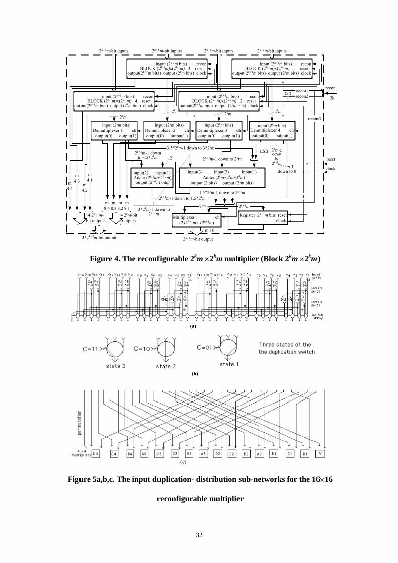
recursively. Figure 4 shows the general scheme of the m2k×m2k multiplier’s structure.
The m2k for k≥1 ( Nk ∈ ) parameter defines the type of the Blocks that are used and the
multiplier itself. The m parameter defines the smallest multiplier and the k parameter
defines the number of the extension that will be made. The recon 1 bits control the kind
of the multiplication that is performed and the pipeline stages of the Blocks, while
recon2 defines the kind of the multiplication of the whole component and if there is
another pipeline stage or not (recon 3). Each m2k×m2k multiplier includes an output
register/latch of m2k+1 bits and a m2k+2 to m2k+1 MUX.
The structure of Figure 4 can multiply two operands of maximum m2k bitwidth. If we
would like to perform m2k-1×m2k-1 multiplications the m2k-1×m2k-1 Blocks would be used.
The four of them can multiply four pairs of multiplicands. We have the choice of
multiplying less pairs of operands i.e. only two pairs of operands, by setting the two out
of the four Blocks in ideal state. The IU (paragraph 2.3) does not transfer data to these

10
two Blocks. Thus half of the structure is used in order to lower the power dissipation of
the unit.
For example, if we use a 4×4 multiplier (m=4) as the smallest multiplier component,
Figure 4 takes the form of the circuit of Figure 3 (Block 8×8). Block 8×8 (m=4, k=1)
differs from the others in two ways. It has two and not three kinds of outputs and is
comprised of four standard multipliers and not from reconfigurable Blocks. The rest of
the Blocks (for k>1) follow the architecture of Figure 4. Thus, to build a 16×16
reconfigurable multiplier (m=4, k=2), four components of Block 8×8, one 3-input 16-bit
carry save adder, one 8-bit ripple carry adder, one 32-bit register and a few additional
multiplexers and demultiplexers (controlled by recon 1,2 and 3 bits) are needed. It is
easy to verify that the architecture can produce the product of two numbers of 16×16 bits
by setting the recon1=1 (of Block 8×8, Figure 3) and recon2=1 (of multiplier 16×16,
Figure 4); or the array of 4 16-bit products by setting recon1=1, recon2=0; or the array
of 16 8-bit products by setting both recon1=recon2=0. In our case the first extension of
Block 8×8 was a structure similar to that of Figure 4 with k=2, a 16×16 reconfigurable
multiplier as the one that was described previously. The other two extensions will be for
k=3 and k=4, a 32×32 and a 64×64 reconfigurable multiplier respectively. This will
happen if we use the proposed 16×16 reconfigurable multiplier as Block 16×16 for
building the 32×32 reconfigurable multiplier and the proposed 32×32 reconfigurable
multiplier as Block 32×32 for building the 64×64 reconfigurable multiplier respectively.
The final reconfigurable multiplier (64×64) can produce an array of 256 products of 8-
bit items in one pipeline cycle; an array of 64 products of 16-bit items in two pipeline
cycles, an array of 16 products of 32 bits in three pipeline cycles, an array of 4 products
of 64-bits in four pipeline cycles, and a 128-bit product in five pipeline cycles. In
general, a reconfigurable m2k×m2k multiplier based on m×m multipliers can execute

11
either, 40m2k×m2k multiplications, or 41m2k-1×m2k-1 multiplications, or 42m2k-2×m2k-2
multiplications, or 43m2k-3×m2k-3 multiplications, …, or 4k-1m21×m21 multiplications or
4km×m multiplications.
2.2.4 The duplication and distribution networks
To duplicate and distribute the input data stream to the array of multipliers, we need
the following two additional simple subnetworks shown in Figure 5, (for the 16×16
reconfigurable multiplier): 1) The input duplication network with the reconfiguration
switches as shown in Figure 5(a) and (b). It duplicates data received from ports in one of
the three levels according to the reconfiguration options and consists of a fixed wire net
and an array of reconfigurable switches with three switch states shown in Figure 5(b)
and 2) The duplicated input data distribution network, as shown in Figure 5(c), is a fixed
wire net, which permutes data to the base 4×4 multipliers. By connecting these two sub-
networks, we have the complete input network. Once the inputs are duplicated and
distributed to the array of base multipliers, the corresponding levels of reconfigurable
modules as described in the previous sections are able to perform the pre-selected
computation in pipeline to yield the desired results. In Figure 5(c) the 4-bit and 8-bit
items have number indicators. If we want to multiply two 4-bit numbers we place them
in the right switches. There is a simple algorithm that finds which the appropriate
switches are, e.g. we place X1, Y1 to switches 17, 1 respectively. The switches are
numbered from the right to the left of the page (Figure 5). For the rest we have what can
be seen in Table 1.
Similarly, the network for a reconfigurable array of multipliers of s=64 (s=maximum
input item bitwidth), m=4 can be constructed, with a total of 512 5-state switches
connected to 256 4×4 multipliers.

12
2.3 Interface unit
2.3.1. Main part
The Interface Unit (IU) distributes an input array pair with h=(s/b)2 b-bit items in
parallel into the MAC and transfers the results out of it. It comprises of two modules, the
one is for the incoming data (input IU) and the other is for the outgoing (output data).
The whole idea is based on correct synchronized multiplexers and trade transfer cycles
(the time needed for a single, 32-bit word to be transferred from/to the bus) for width of
registers. In this approach, we assume a 32-bit input/output bus.
The two basic components for the implementation of the input IU are blocks 1 and 2.
In Figure 6, block1 is depicted. rclk_1 is the complement of clock signal Clk, which the
bus uses to transfer the data. clk_2 is a signal of twice the period of clk and the clk_3 is a
signal of twice the period of clk_2. The two 32-bit registers are provided with new data
by the demultiplexer only when they are triggered by the AND gates. This means that
the 32-bit words that enter into the component are loaded sequentially on the registers
and in every two clock cycles the 64-bit register is loaded. Thus, two sequential numbers
transferred from the bus are forming a single 64-bit number. The blk_select signal
enables, in a way that later will be explained, this block (block1). Block2 has similar
operation, but it uses the clk_2 instead of the clk_3 signal and it does not use the
blk_select signal at all.
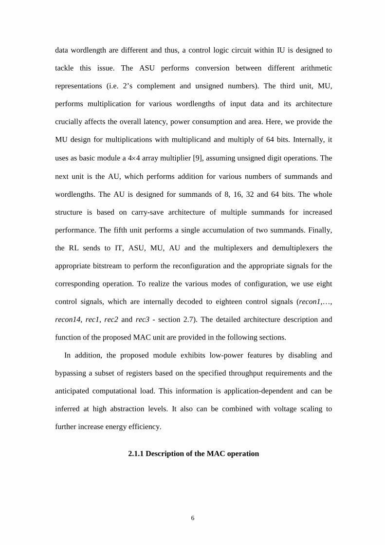
In Figure 7, the whole IU for incoming data is shown. The signal Clk 2 has twice the
period of signal Clk, Clk 4 has twice the period of Clk 2 and so on. Rclk, Rclk 2, Rclk 4,
Rclk 8, Rclk 16, Rclk 32 are the complementary signals of Clk, Clk 2, Clk 4, Clk 8, Clk
16, Clk 32 accordingly.
DeMUX2 distributes the data among the two block1 modules and is controlled by
MUXa. The demultiplexer provides each Block1 module with two sequential data
13
words, because Clk 4 is four times slower than Clk and or it provides only the right
Block1 with data. The signal of MUXa enables each time these blocks to accept or not
accept data by triggering their blk_select input. A period of Clk 4 is the time needed to
load the two block_64 with data.
The output of each Block1 is distributed to two demultiplexers. Their input (a 64-bit
word in each) is driven to the multiplier and or to the next stage of the network. The next
stage is similar but simpler than the first. As we see the components of this stage are
twice the size of the ones in Block1. Block 32 is similar to Block2 with m=64. Recon2
is the signal that determines if 4 pairs of 32-bit numbers will be multiplied or continue in
the same way as before, to the next level for more pairs of numbers of fewer bits.
The reverse procedure is followed after the data are processed, so that they can be
driven back to the bus. This procedure is implemented in the output IU. The new block
that corresponds to block2 is blocka2, as illustrated in Figure 8.
2.3.2 Partial use of the structure-Power reduction
With the addition of a few multiplexers and the appropriate reconfiguration bits, part
of the structure can be disabled. A fraction of the processor’s capabilities are traded for
flexibility and power consumption reduction because of the idle state of the unused part.
In this paper two examples are given for demonstration purposes: i) In Figure 7,
MUXa controls DeMUX3. If Rec3 = ‘1’, the DeMUX 3 passes its input to the right
Block1. Therefore, half the circuit is not in use, leading to no switching activity of its
signals, meaning power consumption reduction. MUXb and MUXc are providing the
new control signals (with half the period from before), for the register and the
multiplexers and ii) in Figure 7, if Rec1 =‘1’, the data from the bus pass to a
demultiplexer. This unit is controlled through the two bits of signal Rec2 and passes its

14
data directly to the multiplication part considering them 4 as pairs of 4-bit numbers
(Rec2=”00”), or 2 pairs of 8-bit numbers (Rec2=”01”) and a pair of 16-bit numbers
(Rec2=”10”). In both examples a large part of the multiplier has been rendered inactive,
leading to great power reduction if it is required.
2.4 Arithmetic selection unit
The arithmetic selection unit (ASU) is comprised of three modules. The first is for the
incoming data, the second for the internal and the third for the outgoing data. The easy
conversion of a binary number to its corresponding 2’s complement one (by inverting it
and adding ‘1’) and of a signed to an unsigned number (by removing and storing its
sign), provides the opportunity to use different arithmetic representation systems on the
same processor. This is possible simply by using the appropriate circuit for converting
the data into a plain unsigned binary number before it enters the multiplier and a circuit
that performs the opposite operation after the multiplication.
The above-mentioned circuit (for the incoming data) forms blocks that process a 128-
bit input each, and one of these blocks is shown in Figure 9. The signals recon1, recon2,
recon3 and recon4 determine if this input is a group of 32 4-bit items or 16 8-bit items
or 8 16-bit items or 4 32-bit items or 2 64-bit items, respectively. Thus, if we choose to
use unsigned numbers, the input ASU is bypassed by the first demultiplexer (both
recon5 and recon6 should be kept low). If the input data will be signed numbers, then
they will be converted to unsigned by setting their sign bit ‘0’ (at the first group of
demultiplexers) and register the 32 sign bits in a separate unit till the data are processed.
These bits are available at the output of the input module for the rest of the ASU
modules. In the case of 4-bit items, the 127th bit, 123rd bit, 120th bit etc, of the register’s
output, which are the sign bits of each 4-bit item, are set to ‘0’. Thus, these numbers are

15
processed like unsigned ones. A similar procedure is followed for all the other groups of
items, setting each time the appropriate bits.
The multiplexers that are used for setting signs are controlled by five single bits,
which are derived from the combinational logic.
The signs of the numbers are registered and at the appropriate time they are examined
through an XOR gate (at the output unit, or at the intermediate unit) and if they are
different (the one is positive and the other negative) the result is ‘1’ (negative number)
otherwise (both positive, both ‘0’ or both negative ‘1’) the result is ‘0’ (positive number.
The output of the XOR gate is connected to the appropriate result bit which represents
the sign of the number. The sign register module (SRM) of Figure 1 performs the simple
operation of registering the values of the signs before they are used at the output or the
intermediate module.
If we want to use numbers in 2’s complement representation we set both recon5 = ‘1’
and recon6=‘1’. The items are inverted and ‘1’ is added to each of them (the addition is
made to the appropriate word derived from the decoder according to the bitwidth of the
operands; e.g.“00010001000100010001000100010001000100010001000100010001000
100010001000100010001000100010001000100010001000100010001000100010001”
for the 4-bit operands), modified in this way to plain unsigned numbers. The inverse
procedure is modifying them back to the original representation system after the
multiplication and addition and it is accomplished in the output module.
The three modules of the ASU are based on the above procedures. The first one (for
the input data) differs from the other two in one element. It cannot convert the processed
numbers to signed representation because it can only remove the signs from the numbers
as can be seen in Figure 9. The other two modules can perform exactly the opposite and
their structure uses a number of XOR gates (as was mentioned above) in order to resume

16
the sign of the numbers. This unit (ASU) is totally independent from the rest unit of the
MAC; therefore it can be used with other modules, for examples reconfigurable adders
or even be disabled at all.
When the incoming data stream of the reconfigurable MAC consists of numbers in
2’s complement, its representation must be changed. First the input data ASU changes
the 2’s complement representation into unsigned digit representation. Then the data are
multiplied and the products enter the internal data ASU, in order to be converted to 2’s
complement representation before they are added. If the original data were not in 2’s
complement representation but in simple signed representation, then the flow of the
processing would be the following: firstly they would be altered to unsigned data,
secondly they would be multiplied, thirdly they would be changed to 2’s complement
representation, fourthly they would be added and accumulated and finally changed into
the original signed representation. In case that we want to perform additions or
accumulations, incoming data in 2’s complement form will be unchanged while signed
incoming data will be changed in 2’s complement representation before the addition.
2.5 Addition Unit
2.5.1 Theoretical basis
This unit is based upon two fundamental properties of addition. Both are
demonstrated using simple examples. In Figure 10, two examples of a binary addition of
four 4-bit numbers and an example of eight 4-bit numbers are shown. The maximum
width of the results of these additions is six and seven bit respectively.
Figure 11 shows an example of the first property of addition that is used in this paper
(property 1). The addition of eight 4-bit (the same as in Figure 10(c)) numbers is
performed in two steps. The first step includes two additions, those of Figure 10(a) and

17
(b). The second step is the addition of the two results of the previous step and their sum
is the same as the one shown in the example of Figure 10(c).
Two conclusions can be derived from this example: The first is that an addition can
be split into a number of additions, with less summands, that are performed in parallel
and vise-versa. The second conclusion is that the addition in this way can be performed
in more than one step, leading to its easy pipelining.
In Figure 12 the addition of the same four numbers as in Figure 10(a) is performed in
two steps (property 2). Each number is split in two parts (of maximum and minimum
magnitude) and in the first step, the four 2-bit numbers of minimum and maximum
magnitude are added (Figure 12(a), 12(b)). The two separate results are added in the
second step, considering that there is a 2-bit magnitude difference between them. The
final result is the same as in Figure 10(a). Therefore the conclusion is, as in the previous
property, that an addition can be split into/composed of a number of additions, with the
same number of summands, but of a smaller word width. The same opportunity for
pipelining is also met in this property.
The adder that is presented here is based on a carry-save structure [9]. The carry-save
addition follows a simple idea: a) more than two summands are used, while the bits of
the same magnitude are added simultaneously, b) in each step, the less significant bit of
the sum and a number of carry bits are calculated from the bits of the same magnitude
(either the bits of the summands, or the carry bits of a previous step). This concept is
explained thoroughly in Figure 13 by using an example of an addition of four 4-bit
numbers (the numbers of Figure 10a). In Figure 13 the carry, sum, and summand bits
are symbolized with the letters c, s and op, respectively. The circled sum bits comprise
the final sum bits.

18
This example uses either 3-bit or 2-bit additions because in the hardware
implementation, either full-adders or half-adders are used. The first step is to calculate
the carry bits and the sum bit of the columns (Figure 13 b1.1, b2.1, b3.1, b4.1). Each
column consists of the bits of the summands, which are of the same magnitude (Figure
13a). In this step the first three bits (sm0_0, sm1_0 and sm2_0) are added and they
produce a carry (c0_0) and a sum (s0_0) bit. Then, the other bit of the summands
(sm3_0) and the s0_0 are added (shaded part), producing a carry (c1_0) and a sum
(s1_0) bit. As it concerns the first column, the calculations are completed and the sum
bit (s1_0) is the less significant bit of the final sum. To calculate the second bit of the
final sum, three more bits are added, the sum bit s1_1 of the second column and the
carry bits c0_0, c1_0 of the first column (Figure 13 (b)). This action results to another
carry (c2_1) and sum (s2_1) bit.
The same procedure continues for all the columns. In Figure 13b is illustrated in
detail, which carry and sum bits are added and how many additions take place in order
to calculate each and every one of the final sum bits.
2.5.2 Basic concept
We use blocks of carry-save adders, which operate as it was explained in paragraph
2.5.1 (Figure 13). They are used either to increase the number of the summands or to
enlarge the width of the summands (by using the first or the second property of addition,
respectively).
The blocks of carry-save adders, that are used here, can add four 4-bit numbers. Still,
their size can be modified according to our demands. In this paper, the only demand,
which we had to take under consideration, is the fact that the multiplication unit (MU)
can produce, simultaneously, at least four products that have to be added.

19
The architecture of each block is based on the structure illustrated in Figure 13.
Every 3-bit addition can be replaced with a full-adder and every 2-bit addition with a
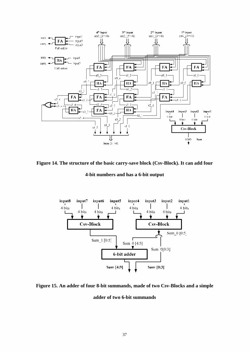
half-adder. The structure of the block is depicted in Figure 14.
Further, we have to notice that the carry-save block (Csv-Block) can be separated in
two parts. The first one is the first four columns of full and half adders, and the second
one is the fifth column of full and half adders and the OR gate. The first part depends on
the number of the bits of the summands. The second part calculates the sum of the final
carry bits that come up from the last column of the first part. If the summands had 8
instead of 4 bits, then the columns of the first part would be eight and the second part
would differ accordingly.
In order to increase the number of the summands, we make use of property 1.
Therefore, to construct an adder of eight 4-bit summands, two Csv-Blocks and an adder
of two 6-bit numbers are used. Each Csv-Block adds four 4-bit numbers and their sums
are added at the 6-bit adder. We can create bigger structures by using more Csv-Blocks
or different Csv-Blocks (in summand width and number). Furthermore, if we want to
add more summands, we can use more Csv-Blocks and replace the 6-bit adder with the
appropriate unit. For example, in order to add sixteen 4-bit numbers, four Csv-Blocks
are used, and the simple 6-bit adder is replaced with a carry-save adder that adds four 6-
bit numbers.
The operand width can be enlarged easily by using property 2. Figure 15 is an
example of how to create an adder of four 8-bit numbers out of two Csv-Blocks and a 6-
bit adder. We can notice that the 6-bit adder can have a simpler structure from a normal
one, because it adds a 6-bit number and a 2-bit number. That is why, we use only its six
bits and not all seven. The seventh sum bit (the most significant bit) of the 6-bit adder
can be set only to “0” because of the summands that are used (the one has six bits, and

20
the other two). Also, notice that only the two most significant bits, of the first Csv-
Block, affect the six most significant bits of the final sum. This is due to the fact that
these are the overflow bits of sum_0. The general observation is that the least significant
bits of the first sum (sum_0) are also the least significant bits of the final sum and only
its overflow bits would affect the most significant bits of the final sum, whichever the
summands width is. For example, if the Csv- Block in Figure 15 was a carry-save adder
of eight 8-bit numbers (its output is a 11-bit number and the three of them are the
overflow) only the three most significant bits are processed further, in order to calculate
the eleven most significant bits of the 19-bit result.
If we want to handle summands of, greater width we can use the same method as in
Figure 15. For example, when we want to add four 16-bit numbers and not 8-bit
numbers as in Figure 15, the only thing that we have to do is use twice the structure of
Figure 15 as it was described earlier. The Csv-Blocks are replaced by components same
as the whole structure of Figure 15 and the 6-bit adder is replaced with a 10-bit adder.
The Most Significant Bit of the 10-bit adder can be set only to “0” due to the used
summands, i.e. the one has six bits, and the other two.
2.5.3 Operation of Addition Unit
The synthesis of the two structures that were described earlier, the one for increasing
the number of the summands and the one for increasing the wordlength of the
summands, yields the reconfigurable addition unit (AU). It is composed of two
modules. The first module comprises identical units in which the main part of the
additions takes place. They are totally independent from each other and that is why they
have the ability to perform different kinds of additions at the same time. Their
architecture is based on carry save addition. The second module is designed in order to
21
combine the outputs of the units of the first section according to the two addition
properties that we explained earlier. Its structure differs according to the number of
these identical units and their structure.
AU can operate as a simple adder or can act as part of an accumulation operation of
the output of the multiplication unit. Therefore it must be able to calculate four kinds of
sums: either four 64-bit numbers, or sixteen 32-bit numbers, or sixty-four 16-bit
numbers or two hundred and fifty-six 8-bit numbers.
We will explain the structure of the AU in two steps. The first one clarifies all the
kinds of the additions that this unit computes except the 256 8-bit number addition,
which is explained in the second step.
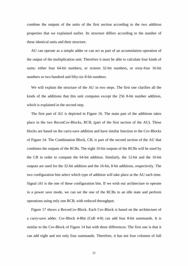
The first part of AU is depicted in Figure 16. The main part of the additions takes
place in the two ReconCsv-Blocks, RCB, (part of the first section of the AU). These
blocks are based on the carry-save addition and have similar function to the Csv-Blocks
of Figure 14. The Combination Block, CB, is part of the second section of the AU that
combines the outputs of the RCBs. The eight 10-bit outputs of the RCBs will be used by
the CB in order to compute the 64-bit addition. Similarly, the 12-bit and the 10-bit
outputs are used for the 32-bit addition and the 16-bit, 8-bit additions, respectively. The
two configuration bits select which type of addition will take place at the AU each time.
Signal cb1 is the one of these configuration bits. If we wish our architecture to operate
in a power save mode, we can set the one of the RCBs to an idle state and perform
operations using only one RCB, with reduced throughput.
Figure 17 shows a ReconCsv-Block. Each Csv-Block is based on the architecture of
a carry-save adder. Csv-Block 4-8bit (CsB 4-8) can add four 8-bit summands. It is
similar to the Csv-Block of Figure 14 but with three differences: The first one is that it
can add eight and not only four summands. Therefore, it has not four columns of full

22
and half adders as the Csv-Block but eight columns and the respective columns for the
addition of the final carry bits. The second difference is that the half-adders of these
eight columns have been replaced by full-adders, so that we can add one more bit in
each column and alter the addition of four summands to an addition of five. The fifth
summand is the result of a previous CsB 4-8 block that we want to use in order to
accomplish an eight-summand addition instead of a four-summand one. With this
modification we have a more fine-grain structure of less area and latency than the one
that was described in paragraph 2.5.2, which employs a separate adder. The third
difference is that demultiplexers, registers and multiplexers are used in order to alter the
number of the pipeline stages as we explained in the multiplication unit. The first four
columns of full-adders of CsB 4-8 (which process the four less significant bits of the
summands) comprise the first pipeline stage and the other four columns of full-adders
(which process the four most significant bits of the summands) comprise the second.
The third stage is the part that adds the final carry bits of the Csv-Block. Two
configuration bits (cb 3,4) determine the number of the pipeline stages.
The Csv-Block 16-8bit (CsB 16-8) is similar to CsB 4-8 with the difference that it
adds sixteen summands instead of four. It is almost four times larger than CsB 4-8 and
they are both based on exactly the same architecture concept. The Demultiplexer Block
1 (DB1) accepts the output of the CsB that precedes and transfers it either to the CsB
that follows (in order to use it to compute an addition of more summands) or to the
output of the RCB. The first three DB1s are controlled by configuration bit 1 (cb1).
When it is set to “0”, the output of each CsB 4-8 is transferred to the next CsB 4-8 and
when it is set to “1”, the sum of a four 8-bit numbers is available at the right output of
RCB. The last three DB1s are controlled by configuration bit 1 (cb2). When it is set to
“0”, the output of each CsB 16-8 is transferred to the next CsB 16-8 and when it is set to

23
“1”, the sum of a sixteen 8-bit numbers is available at the middle output of RCB. The 6th
DB1 if cb2=“0”, provides the left output of RCB with the sum of sixty four 8-bit
summands. The Demultiplexer Block2 is controlled by both cb 1 and 2. When
cb1=cb2=“0” it transfers its input to the next CsB 16-8, when cb1=“1” and cb2=“0” it
provides the right output of RCB with the sum of four 8-bit summands and finally when
cb1=“0” and cb2=“1” it provides the middle output of RCB with the sum of sixteen 8-
bit summands.
The Combination Block (CB) accepts the outputs of the two RCBs (except from the
four 12-bit output of the left one) and computes the final result. The outputs correspond
to the inputs from right to left (as shown in Figure 16). Therefore, by using the two
addition properties, which were explained earlier, the CB includes three structures that
are depicted in Figure 18. The architecture of Figure 18a computes the sum of sixty-four
16-bit summands, the architecture of Figure 18b computes the sum of sixteen 32-bit
summands and the one of Figure 18c computes the sum of four 64-bit summands. These
three circuits are combined to one that is illustrated in Figure 19. The multiplexers and
the demultiplexers select which addition will take place. If cb1=“0” we will have the
addition of the four 64-bit numbers and if cb1=“1” we will have in outputs 1 and 2 the
result of the other two additions.
We will now explain how AU computes the sum of the 256 8-bit summands. The
main idea is to combine the sums of four groups of sixty four 8-bit numbers. So, there
are three implementation options. The first one is to use the two 14-bit outputs from the
RCBs of Figure 16 and another two similar outputs from two Csv-Blocks 64-8. These
Csv-Blocks are simple carry-save structures that add sixty-four 8-bit numbers. The four
14-bit outputs are combined with a circuit of three carry-lookahead adders. The two of
them add two 14-bit numbers each, and their sums are added at a 15-bit adder, yielding
24
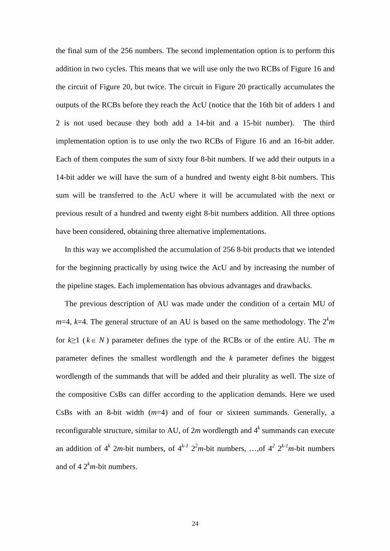
the final sum of the 256 numbers. The second implementation option is to perform this
addition in two cycles. This means that we will use only the two RCBs of Figure 16 and
the circuit of Figure 20, but twice. The circuit in Figure 20 practically accumulates the
outputs of the RCBs before they reach the AcU (notice that the 16th bit of adders 1 and
2 is not used because they both add a 14-bit and a 15-bit number). The third
implementation option is to use only the two RCBs of Figure 16 and an 16-bit adder.
Each of them computes the sum of sixty four 8-bit numbers. If we add their outputs in a
14-bit adder we will have the sum of a hundred and twenty eight 8-bit numbers. This
sum will be transferred to the AcU where it will be accumulated with the next or
previous result of a hundred and twenty eight 8-bit numbers addition. All three options
have been considered, obtaining three alternative implementations.
In this way we accomplished the accumulation of 256 8-bit products that we intended
for the beginning practically by using twice the AcU and by increasing the number of
the pipeline stages. Each implementation has obvious advantages and drawbacks.
The previous description of AU was made under the condition of a certain MU of
m=4, k=4. The general structure of an AU is based on the same methodology. The 2km
for k≥1 ( Nk ∈ ) parameter defines the type of the RCBs or of the entire AU. The m
parameter defines the smallest wordlength and the k parameter defines the biggest
wordlength of the summands that will be added and their plurality as well. The size of
the compositive CsBs can differ according to the application demands. Here we used
CsBs with an 8-bit width (m=4) and of four or sixteen summands. Generally, a
reconfigurable structure, similar to AU, of 2m wordlength and 4k summands can execute
an addition of 4k 2m-bit numbers, of 4k-1 22m-bit numbers, …,of 42 2k-1m-bit numbers
and of 4 2km-bit numbers.

25
2.5.3 The duplication and distribution networks
To duplicate and distribute the input data stream to the AU we need similar networks
to those of the MU that were described in paragraph 2.2.4. The only difference is that in
this case there will be four-state duplication switches because of the four different types
of inputs.
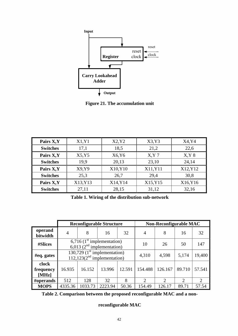
2.6 Accumulation Unit
The accumulation unit (AcU) is a simple circuit that is shown in Figure 21. It
comprises of a two-summand adder and a register. The register holds the latest sum
of the adder and transfers it to the adder to add it to the next available input. In our
structure we chose a carry-lookahead adder because it is one of the fastest
architectures. The maximum sum that exits from the AU (and must be accumulated)
has a width of 66 bits and that would have been the wordlength of the summands of
the adder. But the adder that is used adds two numbers of 128 bits because it is the
widest, in number of bits, product. This product does not pass through the AU
because it is produced once in each time step.
2.7 Reconfiguration logic
The reconfiguration logic (RL) receives as inputs the main clock signal, the reset
signal, and ten internal control signals and performs two main functions: i) internal
clocks generation and ii) decoding of control signals. The input 8-bit reconfiguration
stream is decoded to eighteen control bits whose roles are: i) recon1, recon2, recon3,
recon4 for control bitwidth; ii) recon5 for signed or unsigned number representation; iii)
recon6 for 2’s complement number representation (recon5 ignored); iv) recon7, recon8,
recon9, recon10 for regulate pipeline stages; v) recon11, recon 12, recon13, recon14,
for selecting the function of the whole structure (addition, multiplication, multiplication-

26
accumulation and simple change of number representation); vi) rec1, rec2(2 bits) for
enabling minimum configuration (a 32-bit product, or two 16-bit products or four 8-bit
products); and vii) rec3 for disabling half of the structure (in case of less than half of
maximum throughput).
Depending on the application specifications and the proposed multiplier operate in
many different modes of reconfiguration, choosing the suitable combination from the
internal control signals.
3. Experimental results
For experimental purposes the units of the proposed MAC were described in VHDL
and mapped into a number of Xilinx FPGA devices. This does not mean that the
developed coarse grain architecture is meant for FPGA fine-grain implementations, we
simply used an FPGA prototype to evaluate its performance. We performed
measurements considering a 64×64 reconfigurable multiplier. Specifically, the Input IU
consists of 6150 CLBs or the total equivalent gate count is 122277. The corresponding
measurements for Output IU are: 5463 CLBs and 105432 gates. Each ASU consists of
16 identical blocks each of which includes 334 CLBs or a 5719 gate count. The RL
consists of 463 CLBs and 9432 gates. Apparently, the most hardware complex unit is the
Multiplication Unit (MU). Below, we provide a number of measurements concerning
this part.
Extensive comparative study of the proposed MAC unit, the multiplication unit and
the addition unit with corresponding non-reconfigurable units was performed and the
results are shown in Tables 2, 3 and 4.
In particular, Table 2 provides comparison results between the proposed
reconfigurable MAC and a non-reconfigurable one. Both architectures were

27
implemented on the same Xilinx VirtexII FPGA device. Mega-Operations Per Second
(MOPS) is defined as the number of operations multiplied by the maximum clock
frequency divided by the operation latency in number of cycles. It can be seen that the
area complexity and maximum frequency of the reconfigurable MAC are smaller than
the corresponding numbers of the conventional MAC. However, the proposed MAC can
manipulate various numbers of operands (i.e. 8, 32, 128 and 256 in contrast to the fixed
number 2 of the conventional one. Therefore, the proposed MAC exhibits extremely
high MOPS in comparison to the conventional one. It is obvious that our architecture is
extremely efficient for a big number of operands and as it concerns the area coverage, it
is comparable with the non-reconfigurable MAC if all the functions that our architecture
supports are required. For example, if the proposed MAC is configured to a wordlength
of 8 bits, it can perform 64 operations at a hardware cost of 130,729 equivalent gates,
while conventional MACs an area cost of 64×4,598 gates.
Table 3 shows comparison results among a dedicated array multiplier and the MU for
various bit number of input operands in terms of # CLBs # equ. Gates and MOPS. Thus,
a standard multiplier is better than a reconfigurable one. However, taking into account
the throughput rate (number of results per cycle), the conclusion is that for a large
number of results, the proposed multiplier is faster than a dedicated one and comparable
in area coverage for the same number of parallel products. Also, it is much more
efficient on these parameters if we consider that the MU includes the operation of five
types (i.e. 4×4, 8×8, 16×16, 32×32, 64×64) of multipliers.
In [11], a multiplier that resembles the proposed Block 32×32 was presented,
providing a good opportunity for comparison, and the results are shown in Table 3. The
only parameter that our design is less efficient is the area coverage and because the

28
architecture of [11] was specially designed and characterized on the Xilinx Virtex
device.
The next experimental step was to perform a comparison between a conventional
carry-save adder and the proposed reconfigurable carry-save adder structure. Table 5
shows the comparison results for various bitwidths of input operands and various
numbers of operands in terms of slices, equivalent gates and clock frequency. It can be
seen that the conventional carry-save adder is better than the reconfigurable one in terms
of area coverage and frequency of operation when considering a single function. For this
comparison we had separated the uniform AU in the appropriate parts in order to achieve
a fair comparison. However, taking into account the area coverage, the conclusion is that
if we want to perform all the functions of AU, the proposed adder is much more efficient
(5,190 slices and 60,820 equivalent gates for the 1st implementation of AU, and 3,487
slices and 42,523 equivalent gates for the 2nd implementation of AU). The corresponding
measurements for the four carry-save adders that perform the same operations as AU are
6,392 slices and 74,649 equivalent gates.
Concerning the frequency, a conventional carry-save adder is faster than the
reconfigurable one, since the latter includes additional combinational logic for
supporting the reconfigurable features.
Table 6 shows a qualitative comparison between four reconfigurable architectures.
The common characteristic of the first three is that they support operands of variable
wordlength. The first is the proposed one, while the second, third and fourth were
introduced in [8], [11] and [10] respectively. The term ”variable” means that the
particular design parameter/feature can be dynamically reconfigured within a certain
range by the reconfiguration logic, while “fixed” means that it cannot be reconfigured.
It can be seen that the proposed architecture supports the reconfiguration of more design

29
parameters/features and therefore offers greater flexibility (i.e. plethora of alternative
implementations) than the existing ones. This flexibility makes the proposed
architecture an attractive solution for the implementation of DSP kernels and the design
of larger IP cores. Also, there should be noted that only the proposed architecture
features power-down modes of operation, depending on the application inputs.
Table 7 provides power consumption figures for a Xilinx xc2v3000 implementation
of the proposed MAC that can configured to handle either 16 and 32 bit operands. In the
first case it supports up to 32 operands while in the latter up to 8. It can be seen that the
power consumption is in the order of 100 mW. It should be noted that the specific
FPGA device has a large quiescent power consumption (93 mW) regardless of the logic
implemented on it. Therefore, the actual power consumption of the implemented logic is
less than 40 mW.
4. Conclusions
The design of a reconfigurable multiplication-accumulation unit was presented. It can
be reconfigured in terms of bitwidth, arithmetic representation, throughput rate, and
functionality. Its architecture comprises two principal units, the multiplication and the
addition unit. These two structures can operate both independently as multiplier and
adder and together as a MAC. The superiority of the design is achieved through the use
of sub-multipliers, repeatable parts and totally operation-independent units. This fact
gives the opportunity to power-down part of the architecture, reducing power
consumption and also to use each component or the entire MAC in larger designs as
reusable IP blocks, providing the designer with a number of alternative implementations.
The superiority of the proposed architecture in terms of flexibility was proven by

30
qualitative and quantitative comparisons with similar existing reconfigurable
architectures.
Figure 1. Architecture of the MAC

31
1 st 4x4 m u ltiplier
2 nd 4x4 m u ltip lier
3 rd 4x4 m u ltip lier
4 th 4x4 m ultip lier
A dding a 4-b it num ber in to a 2-bit oneSum m ation of three 8-b it
num bers
16-b it product
Figure 2. An 8×8 product decomposed to 4×4 partial products
Multiplier4 x 4 bit
4-bit inputs
Multiplier4 x 4 bit
4-bit inputs
Multiplier4 x 4 bit
4-bit inputs
Multiplier4 x 4 bit
4-bit inputs
Register 32 bits reset clock
input (8 bits)Demultiplexer 1 choutput(0) output(1)
input (8 bits)Demultiplexer 2 choutput(0) output(1)
input (8 bits)Demultiplexer 3 choutput(0) output(1)
input (8 bits)Demultiplexer 4 choutput(0) output(1)
31 down to 2423 down to 16
15 down to 87 down to 0
input(3) input(2) input(1) Adder (8+8+8)
output (2 bits) output (8 bits)
input(2) input(1) Adder (4+4)
output (4 bits)
31 down to 28
3 down to 0
23 down to 16
7 down to 4
15 down to 8
11 down to 415 down to 12
LSB
27 down to 24
2
1
1
1
m4.4
m4.3
m4.2
m4.1
4 8-bit outputs 16-bit output
reset
clock
m 8
8
8
Multiplexer 1 ch (2x32 to32)
recon7
recon1recon
2
Register 16 bits reset clock
Multiplexer 1 ch (2x16 to 16)
16 16
Figure 3. The reconfigurable 8×8 multiplier (Block 8×8)
32
2k-2
2k+2m-1 downto 3.5*2km
2k+1m-bit inputs
2km2km 2km 2km
input (2km bits)Demultiplexer 1 ch
output(0) output(1)
input (2km bits)Demultiplexer 2 choutput(0) output(1)
input (2km bits)Demultiplexer 3 choutput(0) output(1)
input (2km bits)Demultiplexer 4 choutput(0) output(1)
2k+1m-1 down to 2km
input(3) input(2) input(1) Adder (2km+2km+2km)
output (2 bits) output (2km bits)
input(2) input(1) Adder (2k-1m+2k-1m)
output (2k-1m bits)
3.5*2km-1 down to 3*2km
2k-1m-1down to 0
1.5*2km-1 down to 2k-1m
LSB2
1
reset
clock
recon
input (2k+1m bits) recon BLOCK (2k-1m)x(2k-1m) 4 resetoutput(2k+1m bits) output (2km bits) clock
input (2k-1m bits) recon BLOCK (2k-1m)x(2k-1m) 3 resetoutput(2k+1m bits) output (2km bits) clock
input (2k+1m bits) recon BLOCK (2k-1m)x(2k-1m) 2 resetoutput(2k+1m bits) output (2km bits) clock
input (2k+1m bits) recon BLOCK (2k-1m)x(2k-1m) 1 resetoutput(2k+1m bits) output (2km bits) clock
m4.4
m4.1
m4.2
m4.3
recon1recon2
1 2k
4 2km-bitoutputs
4 2k+1m-bit outputs
2km-1down
to2k-1m
m8.4
m8.3
m8.2
m8.1
3*2k+2m-bit output 2k+1m-bit output
m 16
Register 2k+1m bits reset clock
Multiplexer 1 ch(2x2k+1m to 2k+1m)
2k+1m 2k+1m
2k+1m-bit inputs 2k+1m-bit inputs 2k+1m-bit inputs
3*2km-1 down to2k+1m
2k+1m-1 down to 1.5*2km
recon3
1
Figure 4. The reconfigurable 2km ×2km multiplier (Block 2km ×2km)
Figure 5a,b,c. The input duplication- distribution sub-networks for the 16×16
reconfigurable multiplier

33
input (32 bits) Demultiplexer ch output 1 (32 bits each) output 2
input 64 bits reset Register 64 bits output 64 bits clock
input resetRegister 32 bits output clock
32 bits 32 bits
32 bits 32 bits
64 bits
1 bit
1 bitrclk_1
rst
Output 64 bits
Input 32 bits
clk_2
1 bit
clk_3
blk_select
input resetRegister 32 bits output clock
Figure 6. Block1: first basic component of the interface unit for input data
input m bits resetRegister output m bits clock
Input m bits
Demultiplexer 2 input (m bits) ch output 1 (m bits each) output 2 output 3
Demultiplexer 1 input (m bits) ch output 1 (m bits each) output 2
input m bits resetRegister output m bits clock
Demultiplexer 3 input (m bits) ch output 1 (m bits each) output 2
Input m bits 1 2
Block 1 3 4
Output 2m bits 5
Demultiplexer 4 input (2m bits) ch output 1 (2m bits each) output 2
m bitsm bits
'1'
m bitsm bits
m bits
2m bits2m bits
16m bits
Input 16m bits 1
Block m/8 2Output 32m bits 3
32m bits
Input m bits 1 2
Block 1 3 4
Output 2m bits 5
Demultiplexer 5 input (2m bits) ch output 1 (2m bits each) output 2
2m bits
2m bits
16m bits
Input 16m bits 1
Block m/8 2Output 32m bits 3
32m bits
1 bit
1 bit
1 bit
1 bit
Rec1
Reset
Clk 4
2 bits Rec2
Clk 2Clk
Rec3
Output a
Recon 1Clk 8
Recon 2Clk 16
Clk 32
Recon 4
Clk 64
Output 1
S1
S2
D
CENB
Mux. a
S1
S2
D
CENB
Mux. b
S1
S2
D
CENB
Mux. f
.
.
.
.
.
.
Rclk
Rclk 4Rclk 2
S1
S2
D
CENB
Mux. rf
Rclk 32
Rclk 16
Rclk 8Recon 3
Output 2
Output 3
Output 4
Output 5
Figure 7. Interface Unit

34
input 2m bits reset Register 2m bits output 2m bits clock
input 1 (m bits each) input 2 M ultiplexer ch
output m bits
Input 2m bits
O utput m bits
m bits m bits 1 bit
rst
C lk
Figure 8. Blocka2: Basic component of the interface unit for output data
Figure 9. Arithmetic selection unit for input data

35
1 111
1 01 10 0
Carry bits
Summands
Suma.
10
111 1
+1 0
0
01 01
1 101
0 1 01
000 1
b.
1 11
1 01 01 1c.
1
0
examplea
exampleb
0 1 10
01 01
010 1 0
1
00
1 1 1
+
0
11 11
000 0 0
0
00
1 1 1
+
0
11 11
000 0 0
0
00
Figure 10 (a), (b). Binary addition of four 4-bit numbers (the carry bits are shown),
and (c). Binary addition of eight 4-bit numbers. The first four are those from
example a and the last four from example b
Figure 11. The addition of eight numbers in two steps
10 1 10
01 01
010 1 0
1
00
1 0+
1 01 1
10 10
0 1
Sum110
Step1 Step2
11
+0
01 0
1
1 000
0 1
11
+1
01 1
1
0 001
0 0
2-bitmagnitudedifference
Minimummagnitude bitsMaximum
magnitude bits
Figure 12. The addition of four 4-bit numbers in two steps

36
(b)
0 1 10
01 01
010 1 0
1
00
Foursummands
(a)
4th 3rd 2nd 1st
columns
sm0sm1sm2sm3
010
(c0_3)
(c2_3)(c1_3)
(s2_4)10(c2_4)
+
10 (c3_3)
(c2_4)
(s3_4)10
(c3_4)
+
00 (c2_4)
(c3_4)
(s3_5)00
(c3_5)
+
(c0_3)
sc sm0101
10(s0_3)
(sm0_3)
(sm3_3)(sm2_3)(sm1_3)
(s1_3)01
(c1_3)
010
(s1_3)
(c1_2)(c0_2)
(s2_3)10(c2_3)
+
100
(s2_3)
(c3_2)(c2_2)
(s3_3)10
(c3_3)
+
010
(s1_2)
(c1_1)(c0_1)
(s2_2)10(c2_2)
+
10 (c2_1)
(s2_2)
(s3_2)10
(c3_2)
+
(c0_2)
sc sm1100
01(s0_2)
(sm0_2)
(sm3_2)(sm2_2)(sm1_2)
(s1_2)00
(c1_2)
(c0_1)
sc sm0110
01(s0_1)
(sm0_1)
(sm3_1)(sm2_1)(sm1_1)
(s1_1)00
(c1_1)
000
(s1_1)
(c1_0)(c0_0)
(s2_1)00
(c2_1)
+
sum(s)
carry(c)
summands(sm)
1000
10
(s0_0)(c0_0)
(sm0_0)
(sm3_0)(sm2_0)(sm1_0)
(s1_0)10
(c1_0)
2nd column 1st column3rd column4th column
F0F5 F4 F3 F2 F1
s1_0s3_5 s3_4 s3_3 s3_2 s2_1
Final sum
(c)
Figure 13 a. Four 4-bit numbers separated in four columns according to their
magnitude, b. A detailed example of a carry-save addition
37
Figure 14. The structure of the basic carry-save block (Csv-Block). It can add four
4-bit numbers and has a 6-bit output
Figure 15. An adder of four 8-bit summands, made of two Csv-Blocks and a simple
adder of two 6-bit summands

38
ReconCsv-Block(RCB)
ReconCsv-Block(RCB)
Combination Block (CB)
Figure 16 The first part of the addition unit

39
1st Csv-Block 4-8bit
2nd Demultiplexer1
2nd Csv-Block 4-8bit
1st Demultiplexer1
3rd Csv-Block 4-8bit
Demultiplexer2
4th Csv-Block 4-8bit
3rd Demultiplexer1
1st Csv-Block 16-8bit
4th Demultiplexer1
2nd Csv-Block 16-8bit
5th Demultiplexer1
3rd Csv-Block 16-8bit
6th Demultiplexer1
14-bitoutput
Four 12-bit
outputs
Four 10-bit
outputs
512-bit input4 configurationbits (cb 1,2,3,4)
Figure 17. The ReconCsv-Block

40
14 bitseach
[8:21]
14-bit adder
[0:7]
Input1[8:13]
Input1[0:7]
input1
22-bit Output1
input2
[8:19]
20 bits
12-bit adder
[0:7]
Input3[8:11]
Input3[0:7]
input3input4
[8:19]
12-bit adder
[0:7]
Input1[8:11]
Input1[0:7]
input1input2
20 bits
20-bit adder [16:19][0:15]
[0:15][16:35]
36-bit Output2
12 bitseach
[8:17]
18 bits
10-bit adder
[0:7]
Input7[8:9]
Input7[0:7]
input7input8
[8:17]
10-bit adder
[0:7]
Input5[8:9]
Input5[0:7]
input5input6
18 bits
18-bit adder [16:17][0:15]
[0:15][16:33]
66-bit Output3
[8:17]
18 bits
10-bit adder
[0:7]
Input3[8:9]
Input3[0:7]
input3input4
[8:17]
10-bit adder
[0:7]
Input1[8:9]
Input1[0:7]
input1input2
18 bits
18-bit adder [16:17][0:15]
[0:15][16:33]
34-bit adder
[32:33]
34 bits
[0:31]
34 bits
[0:31][32:65]
10 bitseach
c)
a) b)
Figure 18. The auxiliary circuits for a) a sixty four 16-bit summands addition, b) a
sixteen 32-bit summands addition and c) a four 64-bit summands addition

41
18 bits
32 bits
22 bits
14-bit adder
[0:7]
Mux5[8:13]
Mux5[0:7]
10-bitinput8
[8:17]
10-bit adder
[0:7]
Input5[8:9]
Input5[0:7]
18 bits
18-bit adder [16:17][0:15]
[0:15][16:33]
66-bit Output3
[8:19]
20 bits
12-bit adder
[0:7]
Mux3[8:11]
Mux3[0:7]
[8:19]
12-bit adder
[0:7]
Mux1[8:11]
Mux1[0:7]
20 bits
20-bit adder [16:19][0:15]
[0:15][16:35]
34-bit adder
[32:33]
34 bits
[0:31]
[0:31][32:65]
MUX6 MUX5
10-bitinput7
14-bitinput2
14-bitinput1
10-bitinput6
10-bitinput5
10-bitinput4
MUX4 MUX3
10-bitinput3
12-bitinput4
12-bitinput3
10-bitinput2
MUX2
10-bitinput1
12-bitinput2
12-bitinput1
MUX1
Demux1
[8:21]
Demux236 bits
22-bit Output1 36-bit Output2
cb1
cb1
cb1
Figure 19. The Combination Block (CB)
14 bits
15 bits 15 bits
input2
15-bit adder3
16-bit Output
15-bit adder2 15-bit adder1
15-bit register 15-bit registerclk
14 bits
input1
Figure 20. The auxiliary circuit for the second implementation of the second part
of AU
42
resetRegister clock
Carry LookaheadAdder
Input
reset
clock
Output
Figure 21. The accumulation unit
Pairs X,Y X1,Y1 X2,Y2 X3,Y3 X4,Y4
Switches 17,1 18,5 21,2 22,6
Pairs X,Y X5,Y5 X6,Y6 X,Y 7 X,Y 8 Switches 19,9 20,13 23,10 24,14
Pairs X,Y X9,Y9 X10,Y10 X11,Y11 X12,Y12
Switches 25,3 26,7 29,4 30,8
Pairs X,Y X13,Y13 X14,Y14 X15,Y15 X16,Y16 Switches 27,11 28,15 31,12 32,16
Table 1. Wiring of the distribution sub-network
Reconfigurable Structure Non-Reconfigurable MAC operand bitwidth
4 8 16 32 4 8 16 32
#Slices 6,716 (1st implementation) 6,013 (2nd implementation)
10 26 50 147
#eq. gates 130,729 (1st implementation) 112,123(2nd implementation)
4,310 4,598 5,174 19,400
clock frequency
[MHz] 16.935 16.152 13.996 12.591 154.488 126.167 89.710 57.541
#operands 512 128 32 8 2 2 2 2 MOPS 4335.36 1033.73 2223.94 50.36 154.49 126.17 89.71 57.54
Table 2. Comparison between the proposed reconfigurable MAC and a non-
reconfigurable MAC

43
Dedicated Multiplier Multiplication Unit #bits CLBs # eq. gates MOPS #bits CLBs # eq. gates MOPS 8×8 53 1232 1×34.4 8×8 112 1823 64×54/2
16×16 208 4648 1×18.7 16×16 638 9105 16×54/3 32×32 811 17767 1×16 32×32 2713 39245 4×54/4 64×64 3268 69609 1×13.1 64×64 13501 202609 1×54/5
Table 3. Hardware Complexity (Area) Comparison of a dedicated multiplier and
the proposed multiplication unit
Reconfigurable Structure Conventional Carry-save Adders
#summands –bitwidth/ summand
#slices #eq.gates Clock frequency
(MHz)
#slices #eq.gates clock frequency
(MHz) 4-8 37 615 138.543 37 615 138.543 64-8 1,010 13,113 39.858 864 10,666 53.291 32-16 867 10,818 53.285 843 10,578 58.792
3690 (1st implementation)
40,217 24.675
256-8 1959 (2nd implementation, 2 pipeline cycles)
22,624 27.424 3,632 38,731 32.475
64-16 1,809 22,709 30.450 1,683 20,865 46.013
16-32 822 10,626 55.661 788 10,182 70.279
4-64 343 5,510 59.102 289 4,871 64.470
Table 4. Hardware Complexity (Area)-Frequency Comparison between Carry-save
Adders and a proposed Reconfigurable Structure (RS)
Delay [n]
Slices # of 8×8 products
# of 16×16 products
# of 32×16 products
# of 32×32 products
Proposed Block 32×32 21.251 1416 16 4 1 1
New multiplier 32×9 [11]
23 1108 4 2 1 1
Table 5. Comparison between the proposed Block 32×32 and Corsonello’s et al.
new multiplier 32×9

44
Architecture Wordlength Functions Arithmetic Representation
#Pipeline stages
#Operands
Proposed Variable
MAC, multiplication, addition, data
format conversion
Unsigned, signed, 2’s
complement Variable Variable
[8] Variable Multiplication Unsigned, 2’s complement
Fixed Fixed
[10] Fixed Multiplication Unsigned Variable Fixed
[11] Variable Multiplication Unsigned,
signed Fixed Fixed
Table 6. Qualitative comparison between different reconfigurable architectures
Operand bitwidth #Operands
Max. Clock frequency
(MHz)
Total Power (mW)
Device coverage (slices %)
32 8 12 (one pipeline stage)
118.25 11%
32 8 24 (one pipeline stage)
146.49 11%
16 32 12 (one pipeline stage)
122.49 11%
16 32 24 (one pipeline stage)
153.98 11%
Table 7. Power consumption of proposed reconfigurable MAC

45
References:
[1] J. Hauser and J. Wawrzynek, Garp: A MIPS Processor with a Reconfigurable Coprocessor: in Proc. IEEE FCCM ’97, Napa, CA, USA, (1997), pp.24-33.
[2] E. Mirsky, A. De Hon, MATRIX: A Reconfigurable Computing Architecture with Configurable Instruction Distribution and Deployable Resources, in: Proc. IEEE FCCM ’96, NAPA, CA, USA, (1996).
[3] T. Miyamori and K. Olokotun, REMARC: Reconfiguirable Multimedia Array Coprocessor, in: Proc. ACM/SIGDA FPGA ’98, Monterey, (1998).
[4] H. Singh, et al.: MorphoSys: An Integrated Re-Configurable Architecture, in: Proceedings of the NATO RTO Symp. On System Concepts and Integration, Monterey, CA, USA, (1998).
[5] J. Rabaey: Reconfigurable Computing, The Solution to Low Power Programmable DSP, in: Proc. ICASSP ’97 Munich, Germany, April (1997).
[6] S. C. Goldstein, et al "PipeRench, A Reconfigurable Architecture and Compiler", in: IEEE Computer, Vol.33 No. 4 (2000) 70-77.
[7] R. Hartenstein, A Decade of Reconfigurable Computing: a Visionary Retrospective, Embedded Turorial, Asia-Pacific DAC, (2001).
[8] R. Lin, Reconfigurable Parallel Inner Product Processor Architecture, IEEE Trans. on VLSI Systems Vol. 9, No. 2 (2001) 261-272.
[9] B. Parhami, Computer Arithmetic: Algorithms and Hardware Designs, Oxford University Press, (2000).
[10] S. Kim and M. Papafethymiou, Reconfigurable low energy multiplier for multi-media system design, in: Proc. of IEEE Annual Workshop on VLSI, (2000).
[11] P. Corsonello et al., Variable precision multipliers for FPGA-based reconfigurable computing systems, in: Proc. of FPL 2003, Springer LNCS, 2003, pp. 661-669.

46
Curriculum Vitae
Konstantinos Tatas received his degree in Electrical and Computer Engineering from the Democritus University of Thrace, Greece in 1999. He is currently working towards his Ph.D. in the VLSI Design and Testing Center in the same University. He has been employed as an RTL designer in INTRACOM SA, Greece between 2000 and 2003. His research interests include low-power VLSI design of DSP and multimedia systems, IP core design and design for reuse.
George Koutroumpezis received his degree in Electrical and Computer Engineering from the Democritus University of Thrace, Greece in 2002. He is currently working towards his M.S. in the VLSI Design and Testing Center in the same University. His research interests include reconfigurable VLSI design, IP core design and design for reuse.
Dimitrios Soudris received his Diploma in Electrical Engineering from the University of Patras, Greece, in 1987. He received the Ph.D. Degree from in Electrical Engineering, from the University of Patras in 1992. He is currently working as Ass. Professor in Dept. of Electrical and Computer Engineering, Democritus University of Thrace, Greece. His research interests include low power design, parallel architectures, embedded systems design, and VLSI signal processing. He has published more than 80 papers in international journals and conferences. He was
leader and principal investigator in numerous research projects funded from the Greek Government and Industry as well as the European Commission (ESPRIT II-III-IV and 5th IST). He has served as General Chair and Program Chair for the International Workshop on Power and Timing Modelling, Optimisation, and Simulation (PATMOS). Recently, received an award from INTEL and IBM for the project results of LPGD #25256 (ESPRIT IV). He is a member of the IEEE, the VLSI Systems and Applications Technical Committee of IEEE CAS and the ACM.
Adonios Thanailakis was born in Greece on August 5, 1940. He received B.Sc. degrees in physics and electrical engineering from the University of Thessaloniki, Greece, 1964 and 1968, respectively, and the M.Sc. and Ph.D. Degrees in electrical engineering and electronics from UMIST, Manchester, UK in 1968 and 1971, respectively. He has been a Professor of Microelectronics in Department of Electrical and Computer Engineering, Democritus University of Thrace, Xanthi, Greece, since 1977. He has been active in electronic device and VLSI system design
research since 1968. His current research activities include microelectronic devices and VLSI systems design. He has published a great number of scientific and technical papers, as well as five textbooks. He was leader for carrying out research and

47
development projects funded by Greece, EU, or other organizations on various topics of Microelectronics and VLSI Systems Design (e.g. NATO, ESPRIT, ACTS, STRIDE).
Copyright © 2022 FDOKUMEN