reconfigurable cellular array architectures for molecular ... - DTIC
136
AFRL-VS-TR-2001-1039 AFRL-VS- TR-2001-1039 RECONFIGURABLE CELLULAR ARRAY ARCHITECTURES FOR MOLECULAR ELECTRONICS James Lyke, Greg Donohoe, and Shashi Kama March 2001 Final Report 20010907 126 APPROVED FOR PUBLIC RELEASE; DISTRIBUTION IS UNLIMITED. AIR FORCE RESEARCH LABORATORY Space Vehicles Directorate 3550 Aberdeen Ave SE AIR FORCE MATERIEL COMMAND KIRTLAND AIR FORCE BASE, NM 87117-5776
-
Upload
khangminh22 -
Category
Documents
-
view
1 -
download
0
Transcript of reconfigurable cellular array architectures for molecular ... - DTIC

AFRL-VS-TR-2001-1039 AFRL-VS- TR-2001-1039
RECONFIGURABLE CELLULAR ARRAY ARCHITECTURES FOR MOLECULAR ELECTRONICS
James Lyke, Greg Donohoe, and Shashi Kama
March 2001
Final Report
20010907 126 APPROVED FOR PUBLIC RELEASE; DISTRIBUTION IS UNLIMITED.
AIR FORCE RESEARCH LABORATORY Space Vehicles Directorate 3550 Aberdeen Ave SE AIR FORCE MATERIEL COMMAND KIRTLAND AIR FORCE BASE, NM 87117-5776

AFRL-VS-TR-2001-1039
Using Government drawings, specifications, or other data included in this document for any purpose other than Government procurement does not in any way obligate the U.S. Government The fact that the Government formulated or supplied the drawings, specifications, or other data, does not license the holder or any other person or corporation; or convey any rights or permission to manufacture, use, or sell any patented invention that may relate to them.
This report has been reviewed by the Public Affairs Office and is releasable to the National Technical Information Service (NTTS). At NTIS, it will be available to the general public, including foreign nationals.
If you change your address, wish to be removed from this mailing list, or your organization no longer employs the addressee, please notify AFRL/VSSE, 3550 Aberdeen Ave SE, Kirtland AFB, NM 87117-5776.
Do not return copies of this report unless contractual obligations or notice on a specific document requires its return.
This report has been approved for publication.
iS LYKE, DR Project Manager
FOR THE COMMANDER
KIRT S. MOSER, DR-IV ^ .^ Chief, Spacecraft Technology Division Space Vehicles Directorate

REPORT DOCUMENTATION PAGE Form Approved
OMB No. 0704-0188 Public reporting burden for this collection of information is estimated to average 1 hour per response, including the time for reviewing instructions, searching existing data sources, gathering and maintaining the data needed and completing and reviewing this collection of infomnatlon. Send comments regarding this burden estimate or any other aspect of this collection of Information, including suggestions for reducing this burden to Department of Defense, Washington Headquarters Services, Directorate for Information Operations and Reports (0704-0188), 1215 Jefferson pavis Highway, Suite 1204, Arlington. VA 22202- 4302 Respondents should be aware that notwithstanding any other provision of law, no person shall be subject to any penalty for failing to comply with a collection of information if H does not display a currently valid OMB control number. PLEASE DO NOT RETURN YOUR FORM TO THE ABOVE ADDRESS.
1. REPORT DATE (DD-MM-YYYY) 09-03-2001
2. REPORT TYPE Final
4. TITLE AND SUBTITLE Reconfigurable Cellular Array Architectures for Molecular
Electronics
6. AUTHOR(S)
Lyke, James C. Donohoe, Gregory
Kama, Shashi
7. PERFORMING ORGANIZATION NAME(S) AND ADDRESS(ES)
Air Force Research Laboratory AFRL/VSSE 3550 Aberdeen Ave Kirtland AFB, NM 87117-5776
9. SPONSORING / MONITORING AGENCY NAME(S) AND ADDRESS(ES) DARPA/DSO 3701 N. Fairfax Dr. Arlington VA 22203
3. DATES COVERED {from - To) March 1998 - March 2001
5a. CONTRACT NUMBER N/A 5b. GRANT NUMBER N/A 5c. PROGRAM ELEMENT NUMBER 62601F 5d. PROJECT NUMBER 8809
5e. TASK NUMBER
5f. WORK UNIT NUMBER -= <, <* 6 S C A j. 8. PERFORMING ORGANIZATION REPORT
NUMBER AFRL-VS-TR-2001-1039
10. SPONSOR/MONITOR'S ACRONYM(S)
11. SPONSOR/MONITOR'S REPORT NUMBER(S)
12. DISTRIBUTION / AVAILABILITY STATEMENT Approved for public release; distribution is unlimited
13. SUPPLEMENTARY NOTES
14. ABSTRACT This report is a compilation of largely unpublished work pertaining to reconfigurable cellular arrays for digital computation. They bear resemblance to both cellular automata and cellular neural networks, with the attributes of field programmable gate arrays. They are of potential interest to nano-scale / molecular-scale electronics approaches due to their simple, periodic arrangement. As such they address three critical issues at the smallest physical scales: (1) low-interconnect demand; (2) defect tolerance; (3) simplified construction through non-lithographic approaches (such as chemical self-assembly) . The report exposes many facets of these arrays, including the ability to directly model their structures with artificial neural networks, which can be trained to implement digital functions directly. The report is intended to represent a snapshot of work against a very difficult problem, rich, in future research exploration opportunities
15. SUBJECT TERMS molecular electronics; field programmable gate arrays; neural networks; cellular automata; gigascale systems; interconnections
16. SECURITY CLASSIFICATION OF:
a. REPORT UNCLASSIFIED
b. ABSTRACT UNCLASSIFIED
C. THIS PAGE UNCLASSIFIED
17. LIMITATION OF ABSTRACT
UNLIMITED
18. NUMBER OF PAGES
136
19a. NAME OF RESPONSIBLE PERSON James Lyke 19b. TELEPHONE NUMBER (include area code)
(505)846-5812
Standard Form 298 (Rev. 8-98) Prescribed by ANSI Std. 239.18

TABLE OF CONTENTS
Introduction 1
An architecture for molecular computers ......2
How the molecular architecture achieves fault tolerance 6
Progress report, September 1999 (work performed with Chemistry Department, University of Colorado, Boulder under DARPA / DSO Molecular Electronics) 9
Cellular Automata Based Field Programmable Gate Array Architecture for VLSI and Nanoscale Implementations 19
Progress report, December 1999 (work performed with Chemistry Department, University of Colorado, Boulder under DARPA / DSO Molecular Electronics) 30
Applications of Neural Networks to Lookup Table-Based Circuit Design 45
Proposed Research Effort: Cellular Field Programmable Array Structures for Molecular Electronics 54
Progress report, April 2000 (work performed with Chemistry Department, University of Colorado, Boulder under DARPA / DSO Molecular Electronics) 74
AFRL sub-proposal for the DARPA Moletronics program (Naval Research Laboratory team), November 2000 94
AFRL sub-proposal for the DARPA Moletronics program (University of Colorado / Boulder team), November 2000 106
Progress report, November 2000 (work performed with Chemistry Department, University of Colorado, Boulder under DARPA / DSO Molecular Electronics) 118
Cellular Automata Based Reconfigurable Systems as a Transitional to Gigascale Electronic Architectures 126
u

INTRODUCTION
This compilation contains mostly unpublished work regarding a class of periodic,
reconfigurable architectures that are believed to have great potential for nano- and/or
molecular-scale systems. These reconfigurable cellular arrays (RCAs) are rot really
cellular automata (CA) by some definitions, since they are not necessarily homogeneous
in their state transition matrices and they are directed (feed-forward) networks. They are,
in fact, inspired by CA and field programmable gate array (FPGA) approaches. It is
believed they offer one possible approach to molecular circuits in particular, since it is
hoped that the repetitive sites might one day be realized as a self-assembled arrangement
of complex molecular "nano-blocks" that are, for the most part, identical.
Far from a complete work, this report may well raise more questions than it
answers, whether on a complete implementation of a particular version of a RCA
machine, or on the effectiveness of the architecture with increasing scale, which is a
fundamental concern. Instead, the report is a snapshot, intended to chronicle some
thoughts on problem of architectures that might be built on a molecular scale, with many
stated and unstated opportunities for future exploration. Some of those questions are
being addressed in the continuing work at AFRL, perhaps the subject of future follow-on
reports.

Molecular Field Programmable Gate Array (August 1998, f written May 1998) This architecture is comprised of a large planar (x, y) array of identical building blocks that each implement a single universal, three-input Boolean look-up table (LUT). LUTs are a well-known construct to the designers of VLSI field programmable gate arrays (FPGAs). The LUT is designed to implement any possible function of three Boolean input variables and can be emulated by a eight-bit memory (static flip-flop circuits) that is programmed serially during initialization. By using the three Boolean variables as the inputs of a 8- input multiplexer (built of molecular scale AND, OR, and NOT gates), exactiy one bit of the 8-bit pattern is selected. Since all possible input variations are covered by exactly one output, which can be arbitrarily defined, this LUT universally implements any of the 256 possible Boolean functions of three inputs.
Configuration Bitstream
To next LUT (identical
copy without inverter)
B —i LUT > f(A,B,C)
It is important to understand the power and flexibility of the LUT, as it will enable the construction of a universal computing fabric. A simple k-map representation of three Boolean input variables reveals how eight bits can represent a three-input Boolean function. In the simple example below, the Boolean function f = ABC + ABC + A'BC = AB + BC can be represented by the juxtapositional representation of eight binary digits (e.g., 01001100,11111101, etc.) where each digit represents the functional outcome of a particular point in "Boolean space". The eight bits, which completely specify any conceivable 3- input Boolean function (inputs A, B, and C), can also be represented in decimal. In this example, f(A,B,C)=23+26+27=200, which unambiguously specifies f(A,B,C)=AB+BC.
Other example Boolean functions are shown in the next figure. Not only can traditional functions implemented, but the LUT can be used to emulate wires. For example to connect input A to the output f, one needs only specify the behavior f(a,b,c)=A=#170. This latter feature is essential to the construction of homogeneous logic arrays that can compute more complex functions.

BA
c\ 00 01 11 10
0
1
0 0
0 1
1 3
0 2
0 4
0 5
1 7
1 6
»f(A,B,C) B—H#160 ]—^f(A'B-c)
f(a,b,c)=AOR B f(a,b,c)= A AND C
f(A,B,C) *f(A,B,C) >f(AB,C)
An important and novel feature of the proposed LUT-based computer architecture is in the connection topology, which is based on studies by Wolfram in the propagation of one-dimensional cellular automata.1 Here, we extend the concept to circuit connection topologies, resulting in a homogeneous reconfigurable gate array (see below). The tremendous density of molecular electronics will allow the implementation of arbitrary combinational digital circuits by using standard methods in multilevel logic synthesis and technology mapping, in which complex functions are decomposed into logic building blocks, such as LUTs. In the case field programmable gate arrays, separate algorithms are used to determine placement of the blocks and routing of signals between inputs and outputs of blocks. In the proposed architecture, routing is indistinguishable from logic, which affords new dimensions of flexibility. As this architecture was conceived of fpr molecular level implementation, the relatively inefficiency of using logic for routing is potentially more than compensated for by the sheer density of LUTs that could be implemented. A number of potentially substantial advantages of such an architecture be indicated:
(1) It is an easily iterated structure that can be mass created and extended to very large architectures. Even if Pentiums could be built on a nano-scale, the placement and routing of large numbers of special cells in a fixed arrangement may have the consequences of intractability on various scales, including fabrication and computer-aided-design.

Iterable array based on 3-input lookup tables. Illustrating flow of programming bitstream.
(2) Testability is in principle very simple. It will probably be possible to achieve 100% fault coverage by using the homogeneous network itself to perform testing. Special diagnostic programs can be developed to exercise every wire and node of a complex network, with very little guesswork. Contrast this case with nanoscale, full-custom logic, where even with fault-grading and coverage at 99.99%, an unacceptably high number of failures could go undetected.
(3) The architecture could be very forgiving of faults. Similar to hard disk drives, bad locations could be identified and fed to the logic decomposition and technology mapping software. Algorithms and heuristics for mapping around defective cells in FPGAs could be readily adapted, creating a system that could in most cases implement any conceivable function despite a number of failed regions.
(4) Timing within a block of homogeneously interconnected LUTs is absolutely deterministic since every input signal must pass through the same number of LUTs in order to reach an output. Even when side-coupling is exploited, the number of LUTs involved in a particular computation is known and timing can be establish. This feature is using in timing analysis of very complex designs.
Extending the general computation fabric involves combining blocks of LUTs with "user" storage and providing input/output terminals. One example of such an arrangement is shown below. In this case, two logic array blocks contain m x n LUTs be interfaced through a 1-D array of molecular flip-flops. This arrangement corresponds to the general representation of a combination-sequential digital system (shown right). The flip-flop array exploits side-coupling to provide state preservation, as needed to synthesize finite state machines. In this model all 1-D flip-flops are synchronized with a common clock, limited in frequency only by the total delay represented by 2m flip-flops.

2 i_ co 1- Z> _j
X E
3 I
0) o
>> §-< (0 1- _] c X E
combinational logic
^
flip-flops
Many other arrangements of LUTs and flip-flops are possible. The next figure only begins to hint at the possibilities.
•a *<
1-Darrffy°f ifcLK n flip-flops
1-D array of n flip-flops
mxn LUT array
^ c
so
I Pad
pad
¥ pad
cone of influence"
^ T^
Input / output terminals to the system would be interfaced to the LUT blocks. The sheer density of LUT columns precludes attaching a wire at every LUT. As such, pads would be attached at a pitch dimension
p, selected according to the packaging technology used for the overall system (e.g., 70um for wire bonds, etc.). The inability to place contacts at every LUT column creates a "dead zone" situation, in which the inputs or outputs on particular LUTs are inaccessible. This is due to the fact that in the proposed architecture, each LUT can only connect to the first three nearest neighbors of the preceding row. As such, a "cone of influence" defines the range of interactions possible with LUT arrays from particular points. Algorithmically, these effects are of little consequence to technology mapping software, and it may be easier in the molecular assembly process to simply build those regions in and ignore them in the ensuing implementation of the reconfigurable processing system.
mxn LUT array
"dead zones"
1 Wolfram, Stephen. Cellular Automata and Complexity. Addison-Wesley, New York (1994).

How the Molecular Architecture1 Achieves Fault Tolerance
Fault Tolerance. The fault tolerance of the proposed molecular field programmable gate array architecture is easily shown to be a by-product of its regular structure when combined with appropriate design methodologies and Boolean synthesis heuristics. In the simple example in Figure 1, a set of five input variable (a, b, c, d, and e) are used to generate four functions (hi, h2, h3, and h4). Given the likelihood of many single-point fabrication defects, it is important that architectures for nanoscale electronics be robust enough to deal with random defects.
Row 1-
Row 2-
Row
Row 4 m~
Row
Figure 1. Example logic section (defect-free).
The example logic functions shown perform a variety of Boolean operations on variable (a-e) and generate intermediate results, and eventual generate final functions (hl-h4). To illustrate a potentially likely random defect, Figure 2 shows the impact of a defective LUT in the second row. Based on the cone of influence, most if not all functions dependent on the defective cell are also defective, and the consequences to a non-reconfigurable design would be potentially disastrous.
Row
Raw 3- -*-
Raw 4-
Row 5-
Figure 2. Single random defect.

Fortunately, the ability to reconfigure a vast sea of logic/routing resources makes it possible to readily recover from such defects. An example re-mapping is shown in Figure 3. In this case, the defect is circumlocuted and any ill effects can be safely ignored.
Row I-
Row 2-
Row
Row A w
Row
Figure 3. Circumlocution of single defect.
The key to surviving fault tolerant conditions in such molecular FPGA would be based on several critical requirements:
(1) large pool of reconfigurable (re -defineable) resources; (2) arrangement of these resources to permit sufficient generality (multiple mappings of same functions); (3) process to formally identify defects (functional verification); (4) a set robust Boolean synthesis heuristics to accommodate defects;
The first requirement is met by the present architecture, which is presently the densest proposed reconfigurable system fabric.
The second requirement refers to design methodologies based on the proposed universal computation. It will be necessary to provide "wiggle room" in the design space spanned by the present architecture to permit transparent re-mapping of functions, similar to that shown in Figure 3. Such constraints are met through design disciplines exercised in the course of utilizing the proposed device. It is envisioned as previously described that an entire reconfigurable "chip" would contain many functional sub-domains contain vast tilings of the proposed LUT block structure. Synthesis (in the Boolean sense) would be a hierarchical procedure whereby any subset of the overall system would be partitioned into a given LUT block structure. If the partition is too tightly constrained (resources are too nearly fully prescribed), then a number of point defects would "break" the synthesis at that level, forcing a larger scale backtracking (re - allocation of functional subsets to LUT blocks). In this sense, the lack of "wiggle room" results in a more protracted synthesis, whereby even higher level allocations would need to be re-visited. Part of the architectural research to be carried out in this program will be to establish such "wiggle room" requirements and the effects of functional congestion on synthesis performance.
The third requirement for fault tolerance is the ability to identify defects. Fortunately, the same regular structure lends itself very well to formal verification of device, block, and subsystem functionality through the development of test programmations. As previously suggested, such a capability can be used to establish 100% functional verification.

Finally, the Boolean synthesis system must be "geared" to handle (circumlocute) a finite number of defective LUTs and/or LUT blocks. The realization of complex digital functions from specifications, the common mode of development for complex ASICs, requires the nested solution of many non-deterministic polynomial time (NP-complete) problems in order to arrive at viable solutions in a given medium, whether fixed silicon gate arrays or reconfigurable gate arrays. The process of realization, referred to as Boolean synthesis, generally assumes fully functional resources in the medium, which is probably not a realistic assumption for molecular scale devices. It is necessary, therefore, to consider robust synthesis procedures, whereby a number of known defects, particular to individual devices (identified by a pre-test process), are provided as inputs to the specification procedure, just as the specifications themselves are provided. This situation is analogous to the bad block tables associated with hard disk drives in earlier days of personal computing. Given the bad block map, a hard drive could be formatted in such a way as to ignore defects. We indicate here that a similar approach (in principle) can be applied to achieve maximum yield in molecular devices. It is in fact these fault-tolerant characteristics that may make this very type of architecture the most tractable proposed for nanoscale / molecular scale computational electronics.
1 Lyke, J. "An Architecture for Molecular Computers", white paper, May 1998.

PROGRESS REPORT INPUTS ON MOLECULAR ELECTRONICS ARCHITECTURES James Lyke, September 1999, for the DARPA/ DSO Moletronics Program
One of the most important problems in the design of molecular electronics that must be considered concurrently with the design of basic fundamental building blocks is the architecture that can effectively harness extremely high numbers of logic devices and still meet the constraints of molecular implementation. Ideally, such molecular architectures will be compatible with present-day implementation concepts, or at least they should provide a capability to transition gradual from relatively unconstrained architectures to future ones. This point is very important, as it is clear that even modern semiconductor fabrication processes struggle to keep up with the ideas of architectures without constraints.
This section of the report discusses: (1) the present architecture trends, (2) base constraints in molecular implementation, and (3) a reconfigurable molecularly-scale-able architecture.
1. Present architecture trends.
Evidence that the present trends in VLSI design may not be sustainable is illustrated in Figure 1, which compares the interconnection density of circuits from typical architectures in processes from 1986 and 2005 (projected from the Semiconductor Industry Association) roadmap. Given the present trends, a very large scale integration (VLSI) 0.1 micron integrated circuit might require 10 kilometers of interconnection for each square centimeter of active circuitry. It is on this basis important to understand that the boundary conditions underpinning the current architectural foundations must be re-assessed. These underpinnings include input/output terminal relationships of circuitry, hierarchy, dimensionality, and the descriptive complexity of circuitry.
Figure 1. Interconnection densities in circa 1986 and circa 2005. (left) 1.0 micron process, circa 1986. (right) 0.1 micron process, circa 2005.
The input/output terminal relationship to logic in particular and sub-modules in general is captured by the empirical relationship referred to as Rent's rule. Rent's rule is of the form: T=A*GAp, where T is the number of terminals, A is a multiplicative constant, G is the number of sub-elements (i.e. logic gates), and p is an exponent (Rent's exponent). For VLSI circuitry, it has been shown that for most complex architectures, p is usually in the range 0.6 < p < 0.75, with 0.67 being approximately representative of a microprocessor. In circuit architectures of very high regularity such as memories or systolic arrays, the Rent's exponent is lower, and for random logic, Rent's rule is much higher. Rent's rule can therefore be generally ascribed as a property of architecture. This is very well understood in the high-performance integrated circuit community, particularly by the designers of field programmable gate arrays (FPGAs). FPGAs are complex ICs used to implement seemingly random varieties of digital circuitry. It is the goal of FPGAs in fact, to be completely general, to the point of being able to implement any conceivable digital design. It has, however, been observed that any circuitry, including FPGAs, have a Rent's rule property. Since FPGAs are circuits that try to implement other circuits, then the FPGA, as an implementation medium, has a Rent's rule "supply". The circuits that one wants to implement, of course, have a Rent's rule property, or in other words, a Rent's rule "demand". It has been suggested1 that the "resources" of FPGAs are optimally utilized only when the supply and demand match.

Hierarchy appears to play an important role that is still only qualitatively understood. For example, in graph-theoretic representations of architectures, it has been shown that no Rent's rule exists for random graphs. It appears that the conscious act of design, by humans, leads to the manifestation of Rent's rule. Since humans have the ability to accommodate a very limited span of control, they typically partition complex designs in a modular sense, iteratively until fundamental building blocks are encountered. The resulting iterative decomposition imposes a structure to architectures.
Dimensionality plays a very important role in architectures, particularly in planar integrated circuits. Spatial constraints are an obvious driver to performance, and the tile-like juxtaposition of circuit elements into the floor plan of integrated circuits creates a sort of modulation effect to Rent's rale and to hierarchy. The inability to adequately wire together integrated circuits is partly a consequence of planar (2-D) restrictions. Since elements at a given level of hierarchy are treated in isolation, the interference effect of sub-elements, which compete for the same wiring real estate, is not typically considered in architectural design. At some point, when designs become un-routable in two dimensions, architectures must in effect be comprised in some sense to be implemented, which results in a corresponding decrease in the Rent's coefficient. If circuitry were built in three-dimensions, it is expected that the Rent's rule would change, but even a third dimension would eventually experience a similar bottleneck. Inspiration of non-physical higher-dimensionalities has inspired the implementation of novel architectures such as hypercubes and higher dimensional cellular automata and neural networks. Implementations of such architectures are possible only in simulation or by "flattening" limited instances into 2-D topologies.
One issue with any medium capable of implementing the building blocks of architectures might be referred to as "expressive range". If a proposed universal logic gate has three inputs and can implement any combination of up to three, two-input functions, then it will fall short when an implementation of five, two- input functions is required. The descriptive complexity or Kolmogorov complexity of circuitry has an obvious impact upon its implementation. High descriptive complexities result in dense internal structures in architectural blocks, which will have higher wiring demand. In hierarchical implementations where internal complexity is high but terminal count is low, Rent's rule does not hold true at the system level, but does hold when recursively applied as the system is decomposed into subsystems and elements. Examples of low complexity functions are AND gates and parity functions. Majority gates, which are a function of the Hamming weight of the inputs, are an example of high-complexity functions.
2. Base constraints on molecular implementations
Three immediately obvious constraints have been identified for molecular implementations: (1) low interconnection supply; (2) no tractable lithography; and (3) imperfect medium (defects). Other constraints include thermal handling capability, long range structural stability in use environments (reliability), and packaging.
3. A Reconfigurable cellular automata field programmable gate array architecture for molecular electronics
The baseline tile of LUTs proposed for this program is illustrated in Figure 2. It is based on a 1-D cellular automaton with three-neighborhood. As one might infer, a one-dimensional structure could be implemented as a single row, provided that the computational results are looped back into those structures. This case is shown in Figure 3a, where each cell computes new results based on the local neighborhood about it. If instead the ties are broken (Figure 3b) and propagated forward (Figure 3), a structure is produced as shown in Figure 2. This architecture is interpreted as a 1-D cellular automata structure in which each time step is represented by the next row in the tile.
The architecture is powerful for realizing many useful general and specific computation structures for two reasons: (1) each cell, a three-input LUT (3LUT), can be individual tailored and repetitively re- programmed; (2) each cell may be programmed distinctly with different behaviors. A more complete tile schematic is shown in Figure 4, which shows the previously repressed details on connectivity required for programming each tile. The mechanism is commonly understood and used in traditional VLSI FPGA architectures and is referred to as a bitstream configuration process. Briefly, each 3LUT contains a shift
10

register that is loaded with a binary pattern (personality or "rule"). By cascading all 3LUTs in a tile, a single long bitstream (contains 3*m*n bits for a tile of m rows and n columns) configures each 3LUT in a tile.
Figure 2. Three-input look-up table (3LUT) based tile, a reconfigurable gate array architecture based on cellular automata.
"\ 1 ^ \ IXJXI/ \t) ^J © 0 ^- w
Figure 3. Conversion of 1-D cellular automata to basis for Figure 2 architecture, (left) 1-D binary cellular automat, (center) Removal of feedback, conversion to feedforward, (right) Basic cell for 3LUT tile.
Figure 4. Details showing the configuration bitstream to program each 3LUT in a tile.
Operation of the 3LUT may be gleaned from Figure 5. Each combination of three inputs (A,B, and C) select a particular flip-flop (memory) cell in the shift register structure. The rectangular blocks in Figure 5 represent the circuitry required to effect the storage of a single bit of a shift register chain (referred to as a shift register cell). Since these cells in the shift register are altered by reloading, any of the 2A(2A3)=256 possible binary functions of three inputs can be selectively and directly implemented. Many simple shift registers employ a non-overlapping two-phase clock to advance the bitstream through the register. The bitstream enters a shift-in terminal and exits through a shift out terminal. A summary of the terminals required to implement a 3-LUT follows:
11

77
7?
77
77
77
Function inputs (3): A, B, and C are binary inputs from the output of another LUT or from an outside signal source (for LUTs on the boundaries of a tile). Function outputs (3): Three identical (shorted) terminals output the function of inputs, presumably to other LUTs or to an outside sink (for LUTs on the boundaries of a tile). Configuration clocks (4): Two distinct clocks, phil and phi2, are used explicitly to control configuration of the LUTs. Based on perceived structure of the molecular nano-modules, the proposed LUT configuration will accept and transmit phil and phi2 from a source, and transmit the identical signals, presumably to other LUTs. It is important to note that phil and ph2 are global signals with respect to a tile and must be synchronized by all "members" of the long shift chain in order to advance. It is important and obvious that the clocks are active only during configuration, and these clocks are suspended during normal operation Configuration signals (2): A shift in and shift out signal is required for the purposes of loading the pattern for a particular LUT. Power (2): It is assumed that a single voltage is required for the LUT.
<E_3~W>r
SMIn SMoU ■"■" ""»
"IIP- g~ffpi Pn
Figure 5. More detailed view of 3LUT.
In summary, it is estimated that twelve terminals are required, and four are redundant. The redundancies are anticipated as necessary for the construction of "correct" nanomo dules that could conceivably self assemble in some correct manner. The notion of such a self assembly sequence is depicted with a simplified representation of 3LUTs in Figure 6. The role of redundant terminals is to provide an adequate number of attachment points. As a better understanding of the specific molecular construction is gained, the need (or lack of need) for such terminal redundancy will be established.
Simple representations of the shift register and LUT have developed to provide some bases for possible alternative implementations. If one uses two-terminal gates, a possible representation of a single shift register cell (the contents of the boxes in Figure 5) is shown in Figure 6. The Figure 6 representation is based on the existence of OR and NOT gates, and demonstrates a fundamental need for regenerative logic in molecular implementations that follow a gate-based paradigm. The Figure 6 structure is simply a cascaded, clocked master-slave "SR" type flip-flop, and the regeneration is needed to preserve state. A more generic form of the shift register cell is shown in Figure 7 based on cross-coupled NOT gates and unspecified isolation elements. Figure 7a depicts a non-specific schematic used in VLSI implementations. Once again, the role of regeneration is clearly indicated in the buffered storage required in normal shift registers. Unlike the Figure 6 shift register cell, the Figure 7a version relies on isolation elements to maintain integrity of the contents of each cross-coupled NOT section. The isolation elements could be formed from molecular devices if they can be developed with the ability to gate conduction. Of course, in VLSI design, the isolation elements are implemented with MOSFET devices, as shown in Figure 7b.
12

Shift in
Shift out
Phil Phil Figure 6. Version of shift register based on SR flip -flop that can be implemented with two-terminal OR and NOT gates.
In VLSI implementations, cross-coupled NOT gates are sometimes employed asymmetrically. Figure 7c depicts "weak inverters", which are designed to be "strong" enough to maintain regenerative storage but when the storage value is changed, the source influence is dominant. Some VLSI designs, on the other hand, employ symmetry when bi-directional operation is desired a shift register design.
~^&*^ r3&^ ZW$£h^ \phl2 \ PW2 \PH2
Figure 7. Shift register cell imp lementations. (a) Generic representation, (b) VLSI based, using MOSFETs. (c) Notion of "weak" inverters.
A final, complete schematic for a 3LUT is shown (Figure 8) in a form that can be directly simulated or used in designs. This schematic was generated in the Altera MaxPlus II graphical entry environment and was compiled to verify structural correctness. In this case, the shift registers are implemented as "D"-type flip- flops.
Notional self-assembly of nanomodules to form a tile of 3LUTs. It is expected that a number of LUTs are realized as individual molecules in a chemical synthesis procedure. The nanomodules (about 100 nanometers maximum in physical dimension) might be randomly oriented in a solution. The concept of self-assembly in a grossly simplistic sense involves promoting ä bonding affinity between certain termini on one nanomodule to desired terminal sites on other nanomodules. A depiction of this sequence is shown in Figure 9. The desired objective in this depiction would be a tiled arrangement of LUTs, corresponding to the Figure 2 architecture.
Some preliminary results in application of LUT tiles to routing problems.
The 3LUT tiles have interesting properties, as well as limitations, when considered as a medium for implementing architectural designs. Since the 3LUT tiles are a two-dimensional field of extremely simple computers, complex computations are implemented by decomposition and mapping problems into forms conducive to the constraints of 3LUT tiles. Obviously, among the possible Boolean functions of three- input variables, in addition to traditional logic functions such as AND, OR, XOR, are the wiring functions in which any one of the inputs is selected and simply passed to the output. When only the wiring functions are considered, such as f=A, f=B, and f=C, then the 3LUT tile can be regarded as a wiring manifold. As a wiring manifold, traditional methods used in VLSI gate array design can be used. Examination of the routing characteristics of the 3LUT tile is an important precursor to understanding how to apply the 3LUT to general logic and eventually full sequential digital circuit design.
The case of routing with virtual wires is known to correspond to graph-theoretic treatments. In particular, establishing the optimal connection paths between a set of points is referred to as "forrest" of graph Steiner trees. Finding a single optimal Steiner tree is a known non-deterministic polynomial time complete (NP- complete) problem. For the 3LUT tile, the corresponding graph is directional. This is clearly shown in a simple example for a small tile in Figure 10, which compares the tile schematic (Figure 10a) to a graph representation (Figure 10b). Not surprisingly, the representations are very similar, but when expressed as a graph, the LUT tile can be used as an input representation by existing computer-aided design tools.
13

EHfTJtü
J~>—wr i—i. r tm
Cfi EZ> Figure 8. Complete 3LUT based on elemental gates and "D" type flip-flops.
^
Figure 9. Notional depiction of self-assembly sequence of individual 3LUT nanomodules into a 3LUT tile.
14

To provide some insights into routability, a simple software experiment was undertaken in converting tile representations into graph representations and using an automated routing tool. The source example, shown in Figure 11, illustrates a 10x10 LUT tile with lines depicting a desired input-to-output wiring configuration (input nodes at the top, and output nodes at the bottom). When processed by a simple FPGA greedy router developed for non-directional graphs, a connected pattern employing 3LUTs is produced (Figurel lb). The net contains an incorrect assignment for the 3-5-c wires, which "orphans" the signal input at node 5 (the signal cannot go backward from the node below 4 to the node for signal 3). The routing error is rectified in this example by using a routing heuristic that accepts directed graphs, as shown in Figurel lc. Here, the node represented the merging of signal at inputs 3 and 5 is highlighted. This node would correspond to the output of a 3LUT, which would implement a computation or resolution function of the inputs (3 and 5), producing a result at node c.
b
g h i Figure 10. Graph-theoretic representation of simple LUT tile, (left) 2x3 LUT tile, (right) Graph.
Further examination of the 3LUT may lead to the creation of a new type of Steiner tree problem. In the simple examinations done to date, heuristics for graph problems were used, which are general to non- physical networks. In layout design, other Steiner problem formulations are used, such a planar (two- dimensional Euclidean) and rectilinear (two -dimension LI norm) treatments that take into account the physical constraints of those problems. Clearly, the regularity of the tile structure must give rise it seems to some other type of Steiner tree problem, which may admit better solution heuristics.
Figure 11. Routing example on 10 x 10 LUT tile graph, (a) Example routing problem, (b) Incorrect implementation using undirected graph routing (note 3-5-c net), (c) One possible correct solution.
Another finding of this preliminary work is that the 3LUT is likely the simplest cell design for this architecture that may support the formation of general structures. This is clear due to the fact that whereas it is possible to do virtual wire "crossings" with 3LUTs, it does not appear possible to do this with 2LUTs. In the Figure 11 routing example, wire crossings are readily implemented, though the types of wire crossings and propagation paths are limited. No successful experiments have been conducted in which
15

even the simple results of Figure 11 can be produced with 2LUTs. If conclusive, the finding may be of some importance, since it has generally been assumed that several two terminal gates are capable of supporting universal computation (e.g., NAND, NOR gates). When, however, a regular array of universal two-input Boolean functions are formed, such an array may be extremely restricted in terms of the types of computations that can be performed. When the restriction of regularity is removed, then this statement is not true. In other words, without wiring constraints, an infinite array of universal two-terminal logic gates can universally implement any digital function.
On the other hand, many other tile arrangements can be formed using more complex LUTs. For example, a 4LUT can be used as the basis of a two-dimensional cellular automata definition and another molecular architecture. The cones of influence may disappear in such a formulation, and a new architecture based on 4-LUTs would be capable of local feedback. With a 5-LUT, it is possible to formulate the basis of a cellular automata that can be readily implemented in three physical dimensions. It is also possible to recast the 3LUT tile by replacing each cell with a 5JLUT and extending the connections to the next two nearest neighbors. This formulation is far superior to the 3LUT case, as it allow more sophisticated virtual wiring functions with a much less restrictive "cone of influence" effect. Everything, of course, comes with a price. A 4LUT is, for example, twice as complex as a 3LUT, and a 5LUT is twice as complex as a 4LUT. It is possible to discuss these enhanced versions of the proposed architecture, but it is important to understand more completely the range of use and limitations of the original 3LUT tile (Figure 2) first.
Benefits of present architecture for molecular implementations
The proposed architecture meets a set of constraints outlined previously for nanoscale implementations. First, the architecture is low interconnection demand. It is a medium in which other architectures based on logic and routing are implemented virtually by programming LUTs to perform logic and routing functions. Second, the approach relies on chemical synthesis and self-assembly to create tiles. This avoids the need for lithographic approaches , but due to the reconfigurable nature of architecture allows for delayed definition of circuits that are in effect "soft-loaded" into the tile. This combination of features obviates the need to pattern random and complex structures at a molecular level. Third, the architecture takes advantage of LUTs for the purposes of defect tolerance. Since any LUT can take on any function, then defective zones in an LUT tile are potentially recoverable by ignoring the defective regions and remapping logic and routing around them.
Progress in developing a more complete architectural specification
While the 3LUT tile is an extremely fundamental and important driving theme of a molecular architecture, it is not a complete architectural specification. An attempt to provide a more complete picture of a prospective architecture is shown in Figure 12. The top-level architecture employs a number of 3LUT tiles, juxtaposed through intercalating structures that provide data storage and signal transport, as well as boundary structures, which provide input/output transitions. The tiles are based on a regular arrangement of 3 LUTs in a two dimensional grid. Each LUT is repeatably reprogrammable after fabrication through a configuration bitstream, which is propagated through each element in the tiled structure. The direction arrows refer to the tile orientation. For example, the tile illustrated in Figure 2 is directed downward.
16

CLOCK GEN
JIIL-JII I ■ " '" ■ CLOCK 1OFUFM=L0PS ^jgj^ 1-DFUFM=LC
^MHT LUTTile
IV"
CLOCK GEN
1-DFUPfl.OPs £#~o^
CLOCK GEN
s^X#s ■<s
CLOCK GEN
3
£_
1-0 RIP FLOPS
CLPP< 1-DHJFMR.OPs ~
CLOCK GEN
£^^5 eiiiim
^ CLOCK
GEN 1-OFUP-FLOPs
CLOCK GEN
Figure 12. More complete molecular field programmable gate array, illustrating other support structures.
Provisions of the Figure 12 top-level architecture include:
State preservation and feedback. In order to implement finite state machines and more generalized circuitry, it is necessary to create signal feedback paths. In the Figure 12 architecture, feedback is provided by assembling complete tiles such that: (1) each tile has a different direction of propagation, and (2) if a loop is formed by the tile arrangement. The Figure 12 architecture achieves its "loop" through four tiles, each rotated by 90 degrees. Based on geometric considerations, this results in the need for nanomodules that are equal in size in the two principle axes, and the tiles mist be square (i.e., equal number of rows and columns). It is possible to achieve feedback with only two tiles, as shown in Figure 13. The latter scheme does not require the same degree of symmetry and may be more effective for certain designs.
register file (bit array) ckx* -H 11 i i i iim
m x n iti of LUTs
xtt«äöfLUTs
register file (bit array)
Figure 13. Simpler FPGA architecture, based on only two 3LUT tiles.
Global synchronization. To control the sequential behavior of the resulting implementation, it is necessary to insert a synchronizing structure in the loop. This role is fulfilled by one or more linear (1-D) flip-flop arrays. In the proposed top-level architecture, a number of clock generators, which must
17

themselves be synchronized are employed to "register" all signals emanating from the various tiles. Without this synchronization mechanism, the loop performance of state machines would be path- dependent, which could in fact be exploited in some advanced versions of this architecture. As suggested in the diagram, the configuration bitstreams are also managed by the clock generators.
Input / output. Signals to and from the entire system, the so-called "alligator clip" attachments, are introduced at tile edges. As indicated in Figure 12, these signals may also be registered through flip-flops, though this provision is not required. The considerations for the introduction of input and output signals are manifold, not the least of which include the effects of the cones of influence and the pitch available in electronic packaging assemblies. The "cones of influence" refer to the propagation limits imposed by the signal path constraints in the 3LUT tiles. As shown in Figure 14, the cones of influence do not allow effective utilization of all portions of tiles for input and output. The density of placement or wiring pitch for signals from an external assembly approach (such as wire-bonding) also dictates a fundamental limit of signal density injected into at least the outer tiles. Current wire-bonding pitch state-of-the-art is 50 microns between conductors, and the likely limit of wire-bonding pitch by 2010 will be about 25 microns.
"cone of influence"
pad V
I Pad
pad
J pad
mxn LUT array i< p
m pad
"7 "dead zones"
Figure 14. "Cones of influence" side effect of 3LUT.
Device density remarks. The disparity between terminal density and LUT density are staggering. Assuming 100 nanometer diameter nano-modules and the requirement for square LUTs, an LUT that directly interfaces to the "outside world" and aligns directly to ten, 25 micron bond pads would contain 2500 x 2500 = 6.25 million 3LUTs in a single tile! If the entire perimeter of each of four tiles are utilized, the resulting device would have a total dimension of 0.5mm per side, contain 80 signals and 25 million, 3LUTs. A simplistic extrapolation indicates a 4000 terminal device correlating to a 1 cmA2 molecular integrated circuit with 2500 similar tiles, representing a total of 63 billion 3LUTs in a 2-D "film".
Ultimate extrapolations to a 3-D architecture based on these projections can be attempted. First, it is necessary to understand that the 3LUT template may be inadequate. It is believed that the 5LUT template is the correct correlation for the simplest effective three-dimensional implementation. The 5LUT is minimally four times as complex as a 3LUT. Assuming a nano-module has four times the volume, a three- dimensional tile would contain 3.9E15 5LUTs in a cubic centimeter. De-rating the estimate by an order of magnitude suggests 400 trillion 5LUTs per cubic centimeter. Such projections are grossly simplistic, as many practical issues have been overlooked.
DeHon, A. Reconfiguable Architectures for General-Purpose Computing, AI Technical Report 1586, MIT Artificial Intelligence Laboratory, 545 Technology Sq., Cambridge, MA, October 1996.
18

presented at 8th NASA /IEEE Symposium on VLSI Design, 20-21 October 1999, Albuquerque New Mexico.
Cellular Automata Based Field Programmable Gate Array Architecture for VLSI and Nanoscale Implementations
James Lyke [email protected] Gregory Donohoe ([email protected])
Air Force Research Laboratory
Abstract
The evolution of integrated circuits has shown a steady and dramatic decrease in the size of individual computational elements, and a corresponding growth in device density. As we approach the physical limits of lithography and semiconductor devices, we will need new technologies, such as molecular electronics, to continue the trend toward miniaturization. These devices will require a new design paradigm, with reduced interconnects, and post-fabrication configuration. This paper describes an architecture for harnessing nanometer scale electronics, based on cellular automata (CA). Associated structures are extended to form a field programmable gate array, which may yield new insights into both CA and VLSI applications, and provide a model for designing molecular computing systems.
I. Introduction
It is projected that when integrated circuit (IC) feature sizes approach 0.1 micron, over ten kilometers of wiring will be necessary to interconnect the transistors contained in one square centimeter. Already, interconnections dominate volumetric content. The trend in interconnection density for computational architectures is captured by the well-known Rent's relationship:
Tt kGp
where T is the number of input/output terminals, k is a constant, G is the number of logic gates, and/? is the Rent's exponent [1]. Thus, the number of signals crossing device boundaries is a strong function of the number of gates, resulting in wiring congestion and growth in the average interconnection length. In "gigascale" designs (G > 109) with a Rent's exponent/? > 0.5, the maximum system speed actually decreases due to increased average interconnection length [2]. In today's complex designs, the average Rent's exponent is in the range of 0.65 <p< 0.75. Without some fundamental shift in architectures, further advancement in complex ICs may be stopped by interconnection problems long before we reach the limits of lithography or device physics.
The dramatic progress in microelectronics density is projected to continue for at least the next 12-15 years. After that, devices may be realized as individual molecules, and circuits could be self-assembled through chemical synthesis. Though the theoretical densities of electronics at this scale are high (e.g., » 1018 devices / cc), significant barriers exist:
1. No effective lithographic technologies have been defined for nanometer-scale devices.
19

presented at 8th NASA /IEEE Symposium on VLSI Design, 20-21 October 1999, Albuquerque New Mexico.
2. Interconnection between devices appears to be a fundamentally limiting factor as devices get smaller and VLSI circuits denser.
3. The likelihood of defects will not disappear, but will probably grow at nanometer scales.
This paper describes a prospective architecture, inspired by one-dimensional cellular automata (CA), that may offer a solution to these problems. By spatially unraveling temporal CA architectures, it is possible to form periodic structures with low interconnection demand that can be assembled thorough chemical synthesis. Through cell-specific behaviors, a wide class of Boolean functions can be implemented. This feature, combined with ability to introduce linear register structures, provides a framework capable of directly realizing finite state machines, thus establishing, the basis of a universal computing fabric.
n. Cellular Automata
The concepts of simple CAs are well established and rigorously defined [3,4]. A cellular automata (CA) structure can be thought of as a «-dimensional lattice of one or more point sites (cells). Each site of a CA structure possesses a value, which for the purposes of this paper is either {0} or {1} (i.e., a binary CA). The site values are discrete in time, and the values of all sites change at the same time. The values of each site or cell are updated through a state transition function, or global rule, which depends only on values of cells in a certain local neighborhood, including the cell in question. Figure 1 shows a one- dimensional (1-D) binary CA of neighborhood r=3. The transition from present state to
CA site behavior
111 no poii mo on am 001 ooo o i itT^ 1 i o 1 o
~i i ... * -» ir present value of site present value of left ^ r . TT? , . ...
Q -* next value of site
Global rule formed from Juxtaposing outputs of transition matrixin decreasing lexicographic orxtering of rtaghfcorhoodfc
■'■«: ,"S,:,.,-,-',i'—f~' '.' i." :» i ■#. 0101 lOK}"11'* #90
Figure 1. Example of transition function for 1-D cellular automata with neighborhood r=3. Resulting global rule is a number formed by juxtaposing the output values of neighborhoods in lexicographically-decreasing order: [01011010]= #90.
next state is shown as a function of neighborhood. Since only 23 possible combinations
20

presented at 8th NASA /IEEE Symposium on VLSI Design, 20-21 October 1999, Albuquerque New Mexico.
exist, we can specify the global rule as a decreasing lexicographic ordering of neighborhoods into a binary numeral representation. This simply maps each of the 2 = 256 possible neighborhood combinations uniquely to a particular state transition function. Since all cells have the same global rule, we can describe the behavior of the structure by a single number.
Although simple enough to study rigorously, CA structures can produce complex behaviors. The time evolution of a 79-site 1-D CA is shown in Figure 2. By simply changing the rule number associated with a structure, it is possible to produce four general classes of behaviors: (1) simple (quickly quenched or stable); (2) oscillatory; (3) self-similar, and (4) chaotic-complex. The two-dimensional patterns in Figure 2a represent a time evolution of CA values: columns represent the values at a particular site, and rows represent the site value at particular time steps (time advancing downward). This example illustrates class 3, self- similarity. The pattern is compared to a natural occurrence (Figure 2b), which suggests the ability of CA to directly model certain physical phenomena [4].
(a) (b)
Figure 2. Self-similarity behavioral manifestation in 1-D binary cellular automata, (a) Time evolution of CA with 79 sites, global rule #150, having a single "1" seed initial condition; (b) natural occurrence of self-similarity in patterns found on seashell [4].
CA structures have an initial value of each site at time zero; by virtue of the rule definition, the cell values are unambiguously defined for all future values of time. In trivial CA rules, such as #0, any initial conditions placed on a CA structure are quenched, in this case after a single time step. In other cases, other CA rules are very sensitive to initial conditions. An important set of CA rules, referred to as quiescent, are those that produce a zero value for all time when the initial conditions are zero for the associated sites. Some CA researchers focus only on quiescent CA structures based on desires to correlate behavior with physical phenomena. In the proposed association with VLSI, however, such restrictions are not considered, as they severely limit implementation possibilities (for example, only 32 of 255 possible rules for 3-neighborhood 1-D binary CAs are quiescent).
21

presented at 8th NASA /IEEE Symposium on VLSI Design, 20-21 October 1999, Albuquerque New Mexico.
} {
0
:?
(a)
« p QQQ (b)
popp
(C)
Figure 3: Boundary conditions for CA structures. Top: dangling terminals. Middle: null termination. Bottom: circular termination.
Boundary conditions. We must decide how to treat the nodes at the ends of the structure, indicated by the question marks in Figure 3, top. These nodes can be null terminated, or forced to zero, which produces one set of behaviors (Figure 3, middle.) Alternatively, we can wrap the terminal nodes around to produce a circular structure (Figure 3, bottom).
The state of all or part of a CA structure and its evolution in time can be considered by encoding the values of a vector of sites as a single number. Not to be confused with the rule number, the state value of a it- site CA structure (which spans the range from 0 to 2"-1) is not a specification of behavior, but rather an observation of evolved behavior.
In considering the evolution of state in CAs, two general possibilities exist: reversible and irreversible. Both possibilities are demonstrated in Figure 4 using a single four-site CA structure (1-D, 3-neighborhood). The irreversible case is demonstrated by a circularly terminated structure with rule #90. By encoding the values of the four cells from left to right into a binary number, a state is defined. The evolution of states is shown as a directed graph (Figure 4a), in which the next state value is defined based on the encoding of evolved values that occur at the respective CA sites. For every non-trivial initial condition, the state values merge into common values. For example, initial state values of 1 [0001], 4 [0100], 11 [1011], and 14 [1110] evolve to 10 [1010] in a single time step and then to 0 [0000] after an additional time step. Without prior knowledge, it is impossible from the state value of 10 to establish which of the four possible states led to this value. The ability to reconstruct state history is then defined as irreversibility in this context. By simply changing the boundary conditions from circular termination to null termination, a new state evolution pattern emerges (Figure 4b). In this case, previous state values of the CA structure can be determined based on a given state, which corresponds to reversible behavior. Specifically, the structure produces modulo six, module three, or static (null) behavior strictly based on initial conditions, which suggests the ability to exploit CA for certain sequence generation applications.
22

presented at 8th NASA /IEEE Symposium on VLSI Design, 20-21 October 1999, Albuquerque New Mexico.
T «
"^fi graveyard staie jf ^y
(a) (b)
Figure 4. State behaviors in simple 4-site CA structure with rule #90. (a) Irreversible behavior, (b) Reversible behavior.
m. Reconfigurable Gate Arrays
Reconfigurable field programmable gate arrays (FPGAs) are general-purpose digital circuits whose functions can be altered under software control. Though the original FPGA devices were simple, contemporary devices offer the equivalent of as many as 1,000,000 logic gates.
Many FPGAs implement logic with look-up tables (LUTs), which can be thought of a collection of very simple memory devices (Figure 6). In the example shown, the LUTs have an arity of four, i.e., four inputs and one output. This is equivalent to a boolean
function of four variables, which is equivalent to a 16-bit memory (the number of memory bits is the power set of the arity N of the look-up table, i.e. 2^. Through technology mapping, any logic function can be implemented in four-input LUTs, when loaded with the correct memory contents, and properly interconnected, or routed.
A
B
1
E :F
Wires ~vetti«es Edges - transistors (shown as circles left)
Figure 5. How FPGA architecture is modeled as a graph.
Creating the bit patterns that define FPGA logic and interconnection are among the greatest challenges in
electronic design automation. In routing synthesis, we are given a number of terminal relationships that are defined as the connection scheme between inputs and outputs of LUTs in an FPGA.
A schematic depiction of a portion of a FPGA is shown in Figure 6, illustrating how the routing resources exist in conjunction with two LUTs. The hollow circles at wire intersections represents transistors switches and therefore a potential electrical connections. The dark circles represent closed switches, or completed interconnects, map to edges, as shown in Figure 5.
23

presented at 8th NASA /IEEE Symposium on VLSI Design, 20-21 October 1999, Albuquerque New Mexico.
limn fV X 3 r" 4 1
A\K
m i 2
[4 1
i« ^
mum
B CD A 8 C 0 " FJJt tit -AB: Mj-Ott
(a)
Figure 6. (a) Portion of FPGA, illustrating two look-up tables (LUTs) and some associated routing resources. Small hollow (filled) circles are programmable (fixed) connections, (b) Example routing for F31=AB; F41=CD, simplified view, (c) Same routing showing actual routing resources consumed to form terminal connections.
Complexity of FPGA technology mapping and routing problems. An FPGA design consists of multiple isolated nets. FPGA routing is a serious challenge; some designs may not be routable at all. Most problems involving re-mapping original Boolean specifications into new ones are NP-complete (NPC) [7]. Routing problems on a single net involving more than two terminals are known to be NPC for graphs [8] Typ ical formulations for FPGA nets are as graph Steiner trees [9], and since the vertices represent wires, the resulting optimization problem is a node-weighted Steiner minimum tree (NWSMT).
IV. A Cellular Automata Basis for Field Programmable Gate Arrays
a b f
0 D
<- <-
(a) (b) Figure 7. Direct VLSI implementation of 1-D CA structure (neighborhood of three), (a) Single cell, (b) Iterated structure, showing correspondence to CA.
VLSI implementation of 1 -D CAs with Universal Rules. One-dimensional CA structures can be modeled directly in very large scale integration by combining n-ary logic functions with
24

presented at 8th NASA /IEEE Symposium on VLSI Design, 20-21 October 1999, Albuquerque New Mexico.
state storage structures (D-type flip flops), as shown in Figure 7 for the case of n=3. The individual cell design can be tiled to construct CA structures of any size. The D-type flip flops are connected to a common global clock, which synchronizes updates. If the functions f(a,b,c) are implemented in 3-input LUTs, then they are capable of universally implementing any CA rule for the corresponding template (i.e., any 1-D CA with neighborhood of three). Furthermore, if the LUTs are independently configurable, then the circuit in Figure 7 can implement any non-uniform configuration for CA structures corresponding to the appropriate neighborhood structure.
In order to make the LUT-enhanced architecture of Figure 6 truly feasible and general, we must be able to load the initial state and transition rules. This is easily done with cascaded shift registers controlled by a two-phase clock, as shown in Figure 7.
-LT r
T
T r
V Y -LT
T
-4>o- With these modifications, the resulting circuit may then be considered a cellular automata field programmable gate array (CAFPGA).
Figure 8. CMOS implementation of a shift register-based LUT.
configuration bitstradm for reprog ramming Lllfo
r <-
Lur
r <-
LUT « i q
Applications. CAs can produce a rich variety of behaviors, and reversible CA structures can be exploited as sequence generators. Chang et.al.[10] describe in more detail the use of CA structures to
produce maximum length sequence generators with lower latency than those corresponding to VLSI-based linear feedback shift registers, for the generation perhaps of
keys in cipher streams. Similarly, Tsalides et.al. [11] describe specific VLSI implementations of C A-based pseudo-random number generators (PRNGs) based on additive rules (#90 and #150). Das etal. [12] further consider the use of
JLUT iPfl
• • •
Figure 9. Configuration of 1-D CA with non-uniform rule capability.
C A-based PRNGs to facilitate the development of built-in seiftest structures embedded with VLSI circuitry. The simple CA FPGA previously described provides even greater flexibility in that the rule set can be changed to exploit properties of other CA rules, inhomogeneously throughout the structure as benefits are identified for such implementations.
25

presented at 8th NASA /IEEE Symposium on VLSI Design, 20-21 October 1999, Albuquerque New Mexico.
V. Extensions of the 1 -D CA FPGA to a Flexible Nanoscale Architecture
While 1-D CA structures can be used to perform certain kinds of computations, such as sequence generators, their lack of connectivity makes them difficult to apply to generalized computation problems. Here, we develop a straightforward extension of the 1-D CA that provides a framework for a wide class of digital circuitry, as well as for studying 1-D CAs with time-varying rule structures.
If we consider the 1-D CA structure to actually operate within two dimensions (the second being time), elements of a 2-D architecture which could achieve equivalent results are shown in Figure 10. If the localized dependency structure of a 1-D CA (Figure 10a) is converted into a feed forward network and the temporal registration structures (the D- flip flops) are removed from the direct VLSI implementation, then a simple 1-D nodal network of LUTs is formed (Figure 10b,c). By iterating this single row of LUTs into a series of rows with the appropriate interconnectivity, a two-dimensional structure, referred to as a LUTtile, is formed (Figure lOd). The columns of the LUT tile correspond to an individual CA site. The rows of the LUT tile correspond to the state values of the associated CA structure at particular time steps. This is analogous to arranging time snapshots of a CA structure like a sequence of frames in a strip of motion picture film,
©-^e 0^©^^^
Figure 10. Extension of 1-D CA structure in temporal-spatial CA FPGA. (a) CA dependency template for 1-D CA (b) Feedforward network for single cell, (c) Feedforward network for multiple cells, (d) Complete LUT tile for CA FPGA based on feedfoward netwo rk.
26

presented at 8th NASA /IEEE Symposium on VLSI Design, 20-21 October 1999, Albuquerque New Mexico.
except that the entire "strip" is active. No feedback or memory exist within the tile, and as such the LUT tile emulates a CA of limited temporal and spatial extent.
The goal of conventional FPGAs is to emulate the widest possible class of digital design, and the flexibility comes at a considerable price. It has been estimated that 90% of the silicon real estate in a traditional FPGA is consumed by interconnection structures. By contrast, the LUT tile has limited and simple physical interconnects. Longer-range wiring is implemented by using the LUT as a pass-through connection. Extending this formalism leads to an interesting correspondence between the LUT tile and the FPGA graph structures shown in Figure 5. This correspondence is shown in Figure 11, in which a LUT tile is shown compared to its equivalent graph structure. Assuming a m x n tile with n inputs and n outputs, the corresponding graph will contain (m+l)n nodes and m(3n-2) edges. Like the graphs for traditional FPGAs, the LUT tile graph represents wires as nodes. Edges, however, do not represent routing switches, but rather LUTs that are configured as virtual wire switches. Rule #170 represents a wire connecting only the "left" LUT input to output, rule #204 representing a connection to only the "center" input, and rule #240 a connection to the "right" input. Multiple inputs cannot be "shorted" to the output, but rather a resolution function or computation function must be defined on those inputs, which is usually the case in a feedforward combinational logic network.
An important difference between the Figure 11 graph and the Figure 5 graph is that the former graph is directional. This difference must be accounted for in computer-aided design heuristics. Figure 12 illustrates a simple routing-only example of a 10x10 LUT
tile. Figure 12a depicts the desired wiring configuration. When processed by a simple FPGA greedy router developed for non-directional graphs, a connected set of nets is produced (Figure 12b). The net contains an incorrect net assignment for the 3-5-c net, which "orphans" the signal input at node 5 (the signal cannot go backward from the node below 4 to the node for signal 3). The routing is rectified in this example by using a routing heuristic that accepts
(a) (b) directed graphs, as shown in Figure 12c. Here, the Figure 11. LUT tile and node represented the merging of signal at inputs 3 and corresponding graph for routing. 5 is highlighted. This node would correspond to the (a) LUT tile with three inputs and output of a LUT, which would implement a outputs, (b) Equivalent directed computation or resolution function of the inputs (3 and graph. 5), producing a result at node c.
27

presented at 8th NASA /IEEE Symposium on VLSI Design, 20-21 October 1999, Albuquerque New Mexico.
(a) (b) (c)
Figure 12. Routing example on 10 x 10 LUT tile graph, (a) Example routing problem, (b) Incorrect implementation using undirected graph routing (note 3-5- cnet). (c) One possible correct solution.
Perusal of the Figure 10 LUT tile and routing example results in Figure 12 reveals clear constraints which suggest that limitations exist. One of these is referred to as the cone of influence. This cone of influence, as evident in Figure 12, refers to the limitation in side propagation of signals due to nearest neighbor restrictions. As such, significant excursions of signals "sideways" require many rows in the corresponding LUT tile structure. At a molecular level, where individual LUTs might be molecules, this overhead may be acceptable, and it remains an open problem as to whether this is true in a VLSI implementation. Obviously, the "cone" (which in a graphical construction of LUTs on a square would correspond to 45 degrees) would be enhanced by increasing the neighborhood of the underlying CA. Of course, increasing the neighborhood radius would increase the arity of each LUT, resulting in significantly more complexity n the resulting design. Another clear limitation of the LUT tile is in the implementation of highly complex Boolean descriptions. It would appear that, while more or less true for any FPGA, Boolean descriptions of highly complex structure will "starve" more logic and routing resources. The need to sacrifice LUTs for wire, the cost of routing, and the need to carefully stage wire crossings suggest that the impacts of highly complex Boolean representations may be far worse fcr an LUT tile-based architecture.
VI. Conclusion
To continue the increase in device density, we will have to overcome limitations in lithography and the scarcity of interconnects. The limitations of lithography can be overcome with FPGA-like architectures, in which the device is fabricated first, and then configured to perform its function. The proliferation of interconnects can be corrected with architectures based on local interconnects; cellular automata represent such a class of architectures. This paper has presented a two-dimensional configurable architecture based on cellular automata, and outlined a hardware implementation, and a possible routing strategy. This will serve as a test-bed for research into CA-based configurable FPGAs for general-purpose digital computing.
28

presented at 8th NASA /IEEE Symposium on VLSI Design, 20-21 October 1999, Albuquerque New Mexico.
[I] Donath, W.E. "Placement and Average Interconnection Lengths of Computer Logic", IEEE Transactions on Circuits and Systems, CAS-26(4), April 1979
[2] Bhatt, S.N. and F.T. Leighton, "A Framework for Solving VLSI Graph Layout Problems", Journal of Computer and System Sciences, 28,1984.
[3] Biafore, M. "Cellular automata for nanometer-scale computation", Physica D, 1994
[4] Wolfram, Stephen. Cellular Automata and Complexity. Addison-Wesley, New York (1994).
[5] Pries, W. et.al. "Group Properties of Cellular Automata and VLSI Applications", IEEE Transactions on Computers, volume C-35(12), December 1986.
[6] Lee, Yuh-Sheng and Allen C.H. Wu, "A Performance and Routability-Driven Router for FPGAs Considering Path Delays", IEEE Transactions on Computer-Aided Design of Integrated Circuits and Systems, 16(2): 179 - 185, February 1997.
[7] Zhang,S. etal. "Notes on 'Complexity oif the Lookup-Table Minimization Problem for FPGA Technology Mapping'", IEEE Transactions on Computer-Aided Design of Integrated Circuits and Systems, 15(12): 1588-1590.
[8] Sun, Yachyan, Ting-Chi Wang, C.K. Wong, and C.L. Liu, "Routing for Symmetric FPGAs and FPICs," IEEE Transactions on Computer-Aided Design of Integrated Circuits and Systems, 16(1): 20 - 30, January 1997.
[9] Alexander, M. J., and Robins, G, New Performance-Driven FPGA Routing Algorithms, IEEE Transactions on Computer-Aided Design of Integrated Circuits and Systems, 15(12): 1505 - 1517, December 1996.
[10] Chang, T. et.al. "Maximum length cellular automaton sequences and its application", Signal Processing 56(1977).
[II] Tsalides, Ph. et.al. "Pseudorandom Number Generators for VLSI Systems Based on Linear Cellular Automata", IEE Proceedings-E 138(4), July 1991.
[12] Das, A. etal. "Built-in Self-test Structures Around Cellular Automata and Counters", IEE Proceedings-E 137(4), July 1990.
29

PROGRESS REPORT INPUTS ON MOLECULAR ELECTRONICS ARCHITECTURES James Lyke, December 1999, for the DARPA/DSO Moletronics Program
Relevant architectural concepts must evolve to channel the developments of molecular electronics, particularly given the sheer density and problematic issues associated with the imperfect yield in chemical synthesis. In previous reports, the basic proposal, and in the principal investigator's meeting (July 1999), a special type of architecture was described based on a periodic tiling of look-up tables (LUTs). The previous reports alluded to an essential connection of this architecture to concepts from cellular automata (CA). For the purposes of the present effort, it is not necessary to dwell on the CA basis of the architecture, but rather the characteristics that make it particularly attractive to molecular electronics. In this edition of the report, we briefly revisit these for motivational purposes, as the characteristics of this architecture do address fundamental issues in large scale molecular design. In this section of the report, we will describe a complete specification of a potential architecture hierarchically, from the individual, element gates to the "chip" (system) level. Assumptions are made on some parameters, such as the dimension of a nano- module. We will once again summarize outstanding issues regarding both the specific instance of the architecture, as well as those characteristic of the CA-based architecture in general.
BASIS OF MOLECULAR ARCHITECTURES FOR DIGITAL COMPUTATION
Molecular architectures are capable of achieving at least one million fold functional densities, even in a planar (2-D) form, when compared to contemporary (e.g., 0.25 micron) semiconductor fabrication processes. For arbitrary digital architectures, many of the most challenging problems will appear intractable. For example, no realistic approach to lithography exists at the molecular scale. Self-assembly may provide an alternative approach. However, effecting self-assembly of complex digital architectures based on an arbitrary composition of elemental gates (such as a Pentium) in some brute force scheme on the scale of billions of devices (and much higher) would be problematic. Even if it were possible to form self-assembling arrangements of a complex texture in principle, the problems of defects in synthesis would likely render circuits formed in irregular patterns useless. A potential solution would suggest some ad hoc incorporation of redundant components, even entire circuits. After all, molecular implementations could easily afford to make many copies of the same compfex circuit. More serious studies, however, would reveal that such pronouncements are difficult to realize in practice. In modern integrated circuit design, circuits of complex, irregular structure (such as a Pentium) rely on process control and high yield, whereas circuits of regular structure (such as memories) can systematically exploit redundancy in an easily implemented way. Interconnections will also pose a considerable challenge at a molecular scale, as even today, the effective volumetric content of integrated circuits is dominated by wiring. The number of wiring levels is increasing at an alarming rate, such that without some emphasis on new architectural approaches, the density of future ICs will be interconnection-limited, not gate-limited. In other words, if future architectures cannot be structured to reduce their interconnection demand, the drive for reduced transistor size is irrelevant, since it will impossible to wire them together.
Projecting forward based on the incremental approaches used in the semiconductor industry would lead to futility in terms of defining how to build molecular circuits. It is instead necessary to revisit the problem from the bottom up. Such considerations led to the present architecture. The architecture is hierarchical, similar to the way that ICs and circuitry in complex systems is hierarchical. The most basic level of the architecture requires gates. The first level of "assembly" is based on a collection of gates, referred to as a nano-module. The next level of assembly is referred to as a tile (collection of nano-modules, connected as an x-y planar grid). The highest level of assembly involves combining a number of tiles with other nano- modules and real-world terminal contacts to form a chip.
NANO-MODULES BASED ON SIMPLE LOOK-UP TABLES (LUTs)
In this architecture, we assumed the basic existence of a universal Boolean function set {AND, OR, NOT}. In an abstract sense, it is not important how those gates are built or interconnected. In a practical sense, however, it was known that chemical synthesis approaches would be challenged to assembled complex grids, whether in a regular pattern or not. An upper bound of about 100 gates was suggested as a first level molecular assembly. In this sense, one could define one or more types of nano-modules, each based on an
30

estimated 100 nanometer feature dimension. The nano-modules would have their own terminals, not the type intended for connection to the "outside world", but rather to other nano-modules.
Nano-modules would be bonded to each other, physically and electrically connected through a self- assembly process of chemical synthesis. In this engineered process, the termini of a nano-module would have the highest affinity for particular termini of other nano-modules. These engineered affinities would ideally result in an agglomeration process, whereby perhaps in solution, a collection of "loose" individual nano-modules would eventually build themselves into a tiled arrangement. It would be necessary that the tiles somehow be engineered to terminate in a particular number of rows and columns (when considering a planar arrangement), either in a self-terminating process, or in a process which separates larger manifolds into desired tile pieces.
The concept of tiles of nano-modules is powerful. In principle, each nano-module could be distinct, fabricated from different "batches". Silicon integrated circuits are designed in a similar way, using cell libraries. If we consider each type of nano-module to be letter from an arbitrarily large alphabet, then our tiles could be abstractly considered as strings of letters from the alphabet. Two basic issues exist with this approach. First, the repertoire of "letters" is a considerable engineering effort, each being a separate synthesis process. Second, the rules for forming strings in the alphabet would require considerable investigation. It may not, for example, be possible to connect an "A" to a "U", and so on. While in time, these facets of the nano-module capability could lead to intriguing possibilities, there are too many unknown constraints in a fairly complex design space to permit adequate quantification of all possibilities.
Rather than attempt to establish the entire spectrum of possibilities in the nano-module system, the present architecture considers a limited "alphabet", consisting of a very small number of letters. In fact, the architecture originally proposed corresponded to an alphabet consisting of a single letter. We will eventually show an even simpler architecture corresponding to an alphabet of three letters.
The analogy of nano-modules to letters in alphabet that form strings is a particularly useful one in explaining the coordination of them into tiles. In this explanation, we will restrict the discussion to two dimensions (upon further reflection, the extension to all three spatial dimensions would be obvious). We will consider two examples.
In the first example, we will form strings consisting of only the letter "A". A legal string is simply a block of "As". Examples of legal and illegal strings are shown in Figure 1. The first string (Figure la) is a linear arrangement of letters. The second string (Figure lb) is a two-dimensional array of strings. In our current understanding o f the architectures implicated by the strings, it is usually expected that two -dimensional strings have "straight edges". In other words, though other strings might be legal, such as the one shown in Figure lc, the current concept of our cellular, molecular electronics architecture requires that each row have the same number of letters and each column have the same number of letters. We might call this a normal form. The case where all rows have m letters and all columns have n letters might be called an m x n normal form. Of course, in the Figure 1 example, m=4 andw=5.
The concept of illegal strings is easy to represent in the normal form. If, for example, any letters were not in the correct orientation, then the coordination of those letters would not be correct in an array. Figure Id, for example has three illegal letter sites.
A f-f^-f-^ f^-f-A ^nfnfrtfrA fänfärfy ^-A-A-^ M"t1^
p^^p^ A-TA-A-A-A A-A-A-A rA-A-A-A
(a) (b) (c) (d)
31

Figure 1. Legal and illegal strings in a nano-module alphabet. (a)-(c) are legal strings, (d) is an illegal string.
Of course, the letter "A" is only the symbol for another thing, in particular a nano-module. Our original proposal discussed a tile based on a homogeneous array of 3 -input look-up tables (3LUTs). From a symbolic standpoint, a single 3LUT structure is symbolized by the letter "A", and a tile ofmxn 3LUTs corresponds to a m x n normal form based on a pattern of an alphabet consisting of only one letter ("A"). This symbolism is only a schematic, suggestive of how the particular letters (nano-modules) must be arranged.
In the letter arrangements of Figure 1, short line segments are usually shown between letters. These lines represent connections, perhaps bonds, between the letters. The composition of the connection, including the number of bonds, depends only on which "side" of the letter the line emanates. If we examine our 3LUT tile, shown in Figure 2, which illustrates all non-power connections, we see a definite structure to the types of connections on each side of the LUT. The 3LUT tile corresponds to the m x n normal form (case Figure lb). It is clear that 3LUTs, which correspond to nano-modules, must have the correct orientation and connection to satisfy the relationship implied in Figure 2.
Figure 2. Tile based on three-input look-up table (3LUT) nano-modules, corresponding to Figure lb case.
TWO-INPUT LUTs (2LUTs) AS THE BASIS OF A SIMPLIFIED ARCHITECTURE
In the September 1999 report, we asserted that it was not possible to form a simpler architecture than the planar tile based on 3LUTs. It turns out that assertion was incorrect. While it appears to be true that for the symmetry implied in Figure lb and Figure 2 no simpler tile can be postulated, it is possible to form a simpler tile based on a different kind of symmetry. If, for example, selected links fro m the Figure 2 tile are repressed in a periodic arrangement, it is possible to form a new tile based onrwo-input LUTs (2LUTs). This arrangement is shown in Figure 3a.
32

IW =55 ZUU1 ==S 2UJ- =55 iLUl =55 2LU1
r T T T T (a) (b)
Figure 3. Tile based on two-input look-up table (2LUT) nano-modules and corresponding string in normal form, (a) 5x4 tile of 2LUTs. (b) 5x4 normal form string based on two-letter alphabet.
The new tile requires fewer connections than the Figure 2 tile, and the design of a 2LUT is simpler than a 3LUT. It is also clear that the symmetry involved is not captured in a one-letter alphabet. Now, it is necessary to introduce two different letters, "B" and "C", which are alternated to produce a different set of strings, such as the 5x4 normal form string based on a checkerboard arrangement of two letters.
Once again, the idea of an alphabet of nano-modules is a conceptual convenience. As in a language, strings are composed from letters based on rules of composition. The simple examples so far indicate some utility to this analogy. For the interim, we shall return to consider the 2LUT architecture in more depth. The concept of alphabet as it applies to nano-modules will play a role later as we visit the notion of connecting tiles together.
The 2LUT is shown in Figure 4 in block diagram form. Its operation is described briefly. It is a simple memory structure based on the combination of a shift register of four bits and a multiplexer to select one of the four bits to become the output of the LUT (F_OUT). The selection is driven by two inputs (A,B), which can distinguish four distinct combinations (AB=00,01,10, and 11). Each (A,B) input combination selects one and only one bit of the four to specify the value of the 2LUT output (F_OUT). The values of the four bits are altered only during a configuration process. During configuration, the values of the shift register chain are fed in, one at a time, using a SHIFTJN input to the shift register. The advancement of bits through the shift register is driven by (in this case) a single clock (PHI). During normal operation, the clock is not active (suspended); rather, it is only used to configure the four storage bits of the LUT. By chaining the SHIFT_OUT of one 2LUT into the SHIFTJN of another 2LUT structure, it is possible to configure multiple 2LUTs with the same clock (PHI), fed by the same configuration signal (the SHIFTJN of the first 2LUT). Obviously, this configuration chaining can be indefinitely extended. For the case where many millions of LUTs (or more) are involved, it is a practical consideration to break up a very long "scan chain" into multiple independent chains, fed in parallel. This particular facet of configuration will become important later, when large numbers of LUTs are used to keep configuration time down to a manageable time interval.
33

t, SHFTJN C=? SSj I pa: EE3
"fa:
W
jgL
c»0-
W
k
-CZ3 F_OUT it
Figure 4. Two-input look-up table (2LUT) as a block diagram, based on D-type flip flop storage elements.
The Figure 4 implementation of a 2LUT structure can be re-specified in terms of elemental gates (AND, OR, and NOT gates). One possible implementation, which will become the focus for the nanomodule design, is shown in Figure 5. The shift register implementation is simplified by replacing the D-type flip- flops with elemental D-latches, which are simpler but require a two-phase clock (PHI_1, PHI_2). Otherwise, the Figure 5 implementation is identical to that shown in Figure 4.
The 2LUT contains 56 gates if all needed inversions are counted as individual NOT gates. The gate count is broken into: 20 AND gates, of which 16 are 2-input and 4 are 3-input; 19 NOT gates; and 17 OR gates, 16 of which are two-input and one of which is 4-input. Of the 19 NOT gates, 16 are necessary for operation of the storage elements in the LUT shift register. The other 3 NOT gates are used to eliminate four electrical terminals by forming accessory inversion of the SHIFTJN, A, and B input signals.
Terminal or contact requirements are directly established for the nano-module based on the (1) Figure 5 design and (2) the juxtapositional assumptions for tiling. Based on this design, the 2LUT requires a total of 12 terminals, two (assumed) for electrical power, four for operation, and six for configuration. Electrical termini are assumed to exist universally above and below each nano-module, regardless of type, in the present molecular electronics concept. In fact, the electrical power contacts are generally repressed in the representations shown here. Of the termini required for operation, two are related to the distinct (A,B) inputs, and two are electrically identical output termini, each of which is intended to bond with a distinct neighbor nano-module. Interesting, the configuration requirements dominate terminal count for the 2LUT case. Here, six termini are required for various 2LUT signals, consisting of two electrical identical pairs of clock signals (one pair each for PHI_1 and PHI_2), a SHIFTJN input, and a SHIFT_OUT output signal.
34

a
3 u V
60 C a o a u
•a 3 M
3
■a
o
o a CS a H !=> iJ
1 o o
3
o a o
8 E
>
bO u u
I' o . <J g
u £ t-i .'S

Based on the arguments consistent with a tile architecture based on 2LUTs, the special symmetries and periodic structure require two different nano-module types, which shall be referred to as 2LUT0 (corresponding to "B" in Figure 3b) and 2LUT1 (corresponding to "C" in Figure 3b). The contents of each nano-module are identical, only the nanomodule "shell" itself is different. In particular, the differences in each nano-module related to the engineering of the various termini to have the required affinity to promote selective bonding of the correct termini between adjacent nano-modules. We can attempt to define a more insightful schematic of these nano-modules: these are shown in Figure 6. In these depictions of the nano- modules, the affinities would be highest between termini of the same color. As such, a prospective self- assembly procedure could affect the assembly of many discrete nano-modules into tiles contain 2LUTs connected in an electrically correct fashion, as depicted in Figure 6c.
^^L b'p#iih fg'h d'
Type
Figure 6. Nano-modules for 2LUT architecture, (a) LUT20 ("B"). (b) 2LUT1 ("C"). (c) Depiction of self- assembly sequence, in which the various nano-modules self assemble into a 2LUT tile.
THE TILE ASSEMBLY
Assuming that the significant challenges in the construction and assembly of nano-modules can be overcome, it is important to focus on the specific arrangements of tiles to form a large scale system. Here we must address how large to make tiles. In other words, what is to be the width (n) and depth (m) of a tile? This is the subject of great debate and analysis, as to answer the question completely would require analyzing the "expressive range" of tiles based on Boolean complexity arguments and benchmark testing against a number of examples. Another approach involves making a reasonable first cut estimate, which can be refined pending further assessment of the more abstract architecture considerations. We propose an initial starting point of m=n=70. This choice reflects an initial attempt to form square tiles, and based on an estimated 100 nm nanomodule, this would lead to tiles containing 49,000 2LUTs with a physical size of approximately 7 microns square. If the nano-modules are found to have a different aspect ratio than 1:1, then it may be necessary to alter either m or w accordingly to produce a square tile. Square tiles offer the
36

greatest implementation flexibility, based on our current and limited investigations of more complete architectures, which suggest that when multiple tiles are involved, they may need to be rotated relative to each other. Packing considerations would then dictate a square form factor for the tiles.
Tiles, are themselves only another step upward in the complete hierarchy of a complex molecular architecture. It is necessary to introduce "user storage" into the molecular architecture, and tile boundaries offer a convenient location for register arrays. While, of course, at least four bits of storage are used in each 2LUT nano-module, those storage sites are used to store a bit pattern that implements a combinational function. Altering those bits allow for the expression of any of the 16 possible binary functions of two inputs (2A22), but the bit patterns cannot be accessed under normal operation. Rather, the contents of these memories are affected only by the process of configuration, and are not otherwise alterable during operation. Instead, separate structures are needed to form state preservation for general-purpose digital logic. Furthermo re, the tiles as proposed are feed-forward structures. It is necessary to introduce feedback behavior to form complex digital functions. In consideration of these requirements, we must introduce: (1) a third nano-module type ("D") for user storage, and (2) the concept of rotating tiles to form a feedback structures.
Third nano-module. At least one other nano-module type will be required to form a complete cellular field programmable device. The primary purpose of this third nano-module is to provide a method of holding the output of signals emanating from a tile in synchronization with a global clock. This nano- module is given the designation "D". The first two nano-modules described were necessary to form tiles, which create a generatpurpose media for implementing combinational functions. A third nano-module is needed to implement the following functions: ?? User storage ?? Bitstream management ?? Interface to tiles In this report, we will only describe the requirements of the third tile, but not its implementation, which is still under investigation.
Terminal arrangement A preliminary design of the interface termini needed for the third nano-module ("D") is given in Figure 7a. The nano-module receives the configuration bitstream and distributes it to not only other copies of itself but to the other nano-module types. A typical schematic in the "alphabet-string" format is shown in Figure 7b. Here, two 4 x 5 tiles composed of "B" and "C" nano-modules are "punctuated" by linear sections of "D" nano-modules.
o ? t'3 3
GJJLOCK
SHIFTJN ' PH1.1 PHI2
NANO- MODULE "D"
• SHIFT_OUT | ' PHI_1 ' PHL2 C-B-C-B-C -D-C-B-C-B-C -D
I I I I I I I I I I I I F_OUT_CLOCK OO-D-OD -D-D-D-D-D-D -D
(a) (b) Figure 7. Third nanomodule required for sequential design, (a) Block diagram of single nano-module. (b) "Alphabet string" schematic.
Coordination requirements. The third nano-module type ("D") will interface to the output of either "B" or "C" nano-modules. It is necessary that each "D" nano-module side-couple in a preferred orientation. Specifically, a SHIFT_OUT terminal on one block must connect only to the SHIFTJN terminal of another block. In Figure 7b, a single "D" nano-module is shown in the bottom-right corner, which suggests that the
37

nano-modules can couple in two possible ways. It may in fact be preferable to define a fourth nano-module type, to avoid forming undesired two-dimensional arrays of the "D" type nano-modules.
Operation of the third-type of nanomodule. Linear arrays of nano-modules share a global clock terminal ("G_CLOCK" in Figure 7a). Each nano-module would contain a single user flip-flop, based on an edge- triggered D-type flip flop. The flip-flop array literally "registers" the outputs of an entire tile, synchronizing the states of the last LUT of each column.
Configuration of tiles based the third-type of nanomodule. The complex subtlety of configuration complicates the design of the third tile, which is why this report does not describe a final configuration. The open question remains on how to pass a single or multiple set of configuration bitstreams through all nano-modules so that the contents of each LUT may be deliberately and unambiguously defined. The approach must be robust enough to deal with defects in nano-modules. In Figure 3a, the block diagram suggests that the configuration bitstream is laterally "passed" from left to right. This approach would be disastrous if the bitstream itself was corrupt, since an entire row would not be configurable, leading to blockage of the entire tile. In the notional specification of type "B" and "C" nano-modules, on the other hand, the direction of the configuration bitstream chain is vertical, passing (we suggest) from bottom to top. How then do these columns receive bitstreams? The third nano-module suggests a solution for "bitstream distribution".
The specification is not complete, however. To understand why, it is necessary to briefly discuss how a configuration bitstream is formed. A sample of a short bitstream is shown in Figure 8. This diagram shows a time sequence of three waveforms: "SHIFTJN", "PHI_1", and "PHI_2". The latter two signals refer to the configuration control clocks that govern configuration through shifting data into a chain of shift registers. This clocking scheme is a two-phase clock (non-overlapping), which corresponds to a controlled propagation of signals through a shift register structure. A single period of PHI_1 and PHI_2 corresponds to the movement of one bit through a storage bit in a shift register. Since our LUTs are formed from shift registers, they are configured conveniently by chaining the LUTs together, such that the SHIFT_OUT of the first LUT is fed into the SHIFTJN of the second LUT, etc.
The primary configuration signal is the "SHIFTJN" signal, which feeds something analogous to a "DNA code" that completely specifies the behavior of an entire device (eventually). Based on 2-input LUTs, four bits are required to specify a unique function, so if one billion LUTs are involved, a total of four billion bits or 500 megabytes would be required to specify the total programmation of all LUTs. The pattern of each LUT would simply be fed in one after another at a frequency determined by PHI_1.
0 0 1 0 1 1 0 shiftir
phil
phi2
Figure 8. Example of a configuration bitstream, length 7 bits. >
In principle, then, one only needs to assemble a very long string of zeros and ones, exactly corresponding to the desired contents of LUTs based on the desired configuration of a device. Unfortunately, the likelihood of having a perfect scan chain through a four billion bit shift register is vanishingly small. Furthermore, the uniformity of the LUT nano-module designs results in scan-chains being formed automatically in the process of self-assembly of the "B" and "C" type nano-modules. These chains invariably propagate from bottom to top in the diagrams shown in this report. Yet, obviously, a propagation signal must get from the
38

top of one column down to the bottom of the next column, so that the propagation can continue. A single defect breaks the chain, rendering the entire device potentially useless.
Resolving both problems requires a potentially complex nano-module, which is currently under consideration for the third nano-module ("D"). One approach for bitstream distribution is based on allowing the third nano-module to "steer" the propagating bitstream, using cues embedded within the bitstream to steer the direction. A simple diagram (Figure 9) will serve to illustrate one potential scheme that could be implemented with a simple state machine that could be implemented within the "D" nano- module. Figure 9 represents a linear array of "D" nano-modules, connected at the bottom of a tile of LUTs (not shown). When the "system" is initialized, a bitstream is fed into the left-most type "D" nano-module. By default, each type "D" nano-module "steers" configuration data upward into the LUTs above the particular "D" nano-module. Each LUT is configured by an arbitrary four bit code (0000 through 1111). We define a convention that requires a single zero bit be inserted between each LUT. So if three LUTs each contain all ones, the actual bitstream would be defined as: 111101111011110. This representation is not compact, but permits the definition of a simple escape code, containing five one bits: 11111. When the escape code is encountered, the type "D" nano-module detects the code and "steers" the direction of bitstream propagation from "up" to "right". This is an extremely simplistic implementation of a self- routing message, in which the content of the bitstream itself provides cues for how the overall device is configured.
The use of self-routing codes have additional benefits. For example, defective columns can be bypassed by simply form two consecutive patterns of five ones, which would force two switches to steer without any configuration operations occuring in the bypassed columns. Once a bypass is set, it would never be reversed for the remainder of the configuration process.
§ S S S I f f f 1 1
D - -► D - - D - - D - -. D
L X J
"inn f f 1 —■ D —■ D —' D
(b)
(<0
(d)
Figure 9. Use of escape codes in "D"-type nano-modules to implement robust configuration bitstreams.
How would such a self-router be implemented? The simplest approach is to make a simple state machine built from three additional flip-flops that are hidden within the nano-module. The state machines would: (a) "eat" the delimiting zero between LUT code blocks, and (b) detect a sequence of five one's and alter direction based on its occurrence.
TILE JUXTAPOSITION
In order to form a complete molecular electronics system, it is necessary to form a hierarchical grouping of tiles, which are themselves based on a grouping of various nano-modules. If the dimension of the nano- modules are about 100 nanometers, then a 100 x 50 tiling of nano-modules would require a 5 micron x 10 micron molecular block. This dimension is much smaller than a human hair. In fact, a standard bonding wire used in integrated circuits is 25 microns in diameter. Obviously, the tile is not a very useful device by itself.
Instead, we consider a "tile of tiles". Why not simply build a larger tile? It is due to primarily to the exponentially growing complexity of combinational Boolean functions. Similar arguments are used to
39

justify using 2-input or 3-input LUTs instead of 500-input LUTs. A 500-input LUT would require a 2500
shift register, which exceeds the number of particles in the known universe. A 100,000 x 100,000 arrangement of 2-input LUTs, unlike the 500-input LUTs, can be built. Unfortunately, the implementation complexity of Boolean functions is almost always exponential in the number of inputs. LUTs, of course, embed exponential complexity for their input space. In other words, a 3-input LUT has 23 storage bits and can therefore implement any function of three inputs. Random Boolean functions of say 16-inputs (generated by populating a truth table with the results of 216=65,536 coin tosses) would require 0(216"m) m- input LUTs to implement. As such, very large combinational functions are either intractable or can be expressed in more compact forms. For example, a 100-input AND gate can be expressed in O(log2100) 2- input AND gates. Neither extreme is serviced by implementing a very large tile. For the simpler cases, the vast majority of LUTs would be wasted, and for the complex cases, the intractability concern would make perceptibly finite implementations impractical. Based on these arguments, it would make more sense to form smaller tiles, which could be grouped together to imp lement more complex functions, not intractably complex, but of the order of complexity of those Boolean systems which are implemented today, even those one million times more complex.
In the juxtaposition of tiles, we assume the introduction of linear (type "D") sub-modules between each tile interface. If the goal is to form a device of reasonable physical extent (say 1 cm square), then we would find that it is possible to assemble a 1000 x 2000 grouping of tiles, which would then be the basis of a one- billion LUT system.
PRELIMINARY CONSIDERATIONS OF REAL-WORLD INTERFACE
What about the "alligator clips" or real-world interface? If, for the time being we assume perimeter contacts (bond pads at the edges of the large device), the state-of-the-art by the year 2010 will be about 25 microns between terminals, or about 1,600 terminals in a square centimeter.
There is "good news" and "bad news" in this line of pursuit. To expose these points, we need only begin a superficial consideration of Rent's rule. Rent's rule is an empirical relationship between the number of gates in a device and the number of terminals normally required:
T=AG° where Tis the number of terminals ("alligator clips"), G is the number of gates, 0.5 <p < 0.9 is Rent's exponent, and A is a multiplicative constant (some authors refer to this as the number of pins per block). Considerable work has been done in the literature to examine trends represented by actual integrated circuits, with always the inevitable result of reinforcing the largely empirical Rent's rule relationship. As a current "datapoint", we can consider a typical gate array, such as the Altera (San Jose, CA) 10K100 gate array, which has a value of T= 400 and G =-105. By selecting A = 1 and p = 0.5, we substitute G = 105 and find a projected value of T= 316. While that projection is slightly low, we note that point and now simple replace the value of G = 109, only to find the project value of T > 30,000. This is, of course, about a factor of 20 above the initial specification of T= 1,600. If we were to insist on reflecting the choices of A and/7 to "fit" T, the values would be unrealistically low (i.e., A«\ and/orp «0.5)
There are two ways to interpret the result. First, we need many more terminals to exploit the present design. Should me terminal count goals be revised upwards? If we assume an areal distribution of "alligator clips" then we must relax the pitch requirements due to real world issues of interconnect, but obviously we are easily able to look at 10,000+ alligator clips on one chip. We have not considered this possibility in great depth, because: (1) our current power delivery approach involves access to the "top" and "bottom" of circuitry, which could occlude access the signal termini, and (2) in three-dimensional extensions of the present approach, we would now consider the top and bottom surfaces to be interior connections, not external. The second interpretation is that the Rents' Rule based on a global system (chip) is no more demanding man what the underlying design hierarchy "can deliver". In other words, the
40

external interconnections are far more limiting than the internal limitations. This seems encouraging at first pass, since we had fundamental concerns about internal connectivity. This latter interpretation is not satisfying, however. It may be, for example, that a complex system has a hierarchy-dependent Rent's rule. To understand this suggestion, consider that a complex system can be severed or partitioned into a number of pieces, say from 4-10 partitions. Each partition will have its own Rent's rule behavior. Then, consider a partition ofthat partition, and repeat this process recursively until a fundamental element, such as an LUT, is encountered. At each recursive level, the Rent's rule behavior will generally be different. For high-performance systems, it may be in fact necessary to sustain a higher Rent's exponent at intermediate levels of the hierarchy. In a personal computer, for example, considered as a system, the "box" will contain billions of transistors, but in fact has a low Rent's rule behavior, as represented by the number of pins in the serial ports, video connector, etc. If one were to arbitrarily chop the personal computer into two sections, the Rent's rule behavior of the two pieces would in general be quite different. It would not be unusual to find many tens of thousands of conductors severed in such a bisection, considering the circuit board traces and integrated circuit wires that would be exposed. Simply put, Rent's rule analyses must be considered carefully. That Rent's rule is still a largely empirical result does not make this analysis any easier.
Summary of the molecular "chip".
We provisionally maintain that the recommended terminal count of 1,600 is workable, pending further analysis. These assumptions now allow us to define an emergent picture for the first time of a molecular ele ctronics "chip". The chip would have a planar construction, with a physical size of about one centimeter square. The number of terminals would be about 1,600 signals, with independent power delivery. In other words, the 1,600 terminal count does not include power and ground. The signal terminals would be located at the perimeter of the device, spaced at a 25 micron pitch, which is consistent with the emergent packaging infrastructure within the next 5-7 years. The molecular chip would contain 1000 x 2000 tiles. Each tile would contain 100 x 50 look-up tables (LUTs). These LUTs are capable of implementing any arbitrary 2-input Boolean function, and the tiles would also contain perimeter data storage structures, permitting complex digital combinational and sequential design. Since the data structures are at the perimeter of tiles, and we "count" only two of the four edges of each tile, this would provide an aggregate of one billion reconfigurable gates with 300 million bits of user storage. What do these capabilities mean in terms of real worlds, present day capabilities? One crude estimate is that this raw number of physical resources is capable of implementing 500 separate Pentium-class processors on a single chip. Since the gates are completely reconfigurable {as for example, the Teramac or any other "garden variety" field programmble gate array), it is of course possible to "refocus" the gates in problem-specific, optimal ways. We have yet to establish the operating frequency capability of such a molecular chip. If we assert that at least a 10 GHz cyccle tie is possible, then iit is theoretically possible to achieve 1019 operations/second from such a chip. Not bad for a thin scum of planar circuity! If we are further able to exploit a third dimension, then we could multiply thsi theoretic number by the vertical density of molecular layers. Some suggestions of an additional million-fold density achieved by exploiting the third dimension would lead to a theoretical performance of 1025 operations / second. If a Pentium is a" 109 machine", then this would in some stretch represent the capability of 1016 Pentiums!
Some caveats must be considered however. Just as the Termac makes a 1012 operations/second claim, this is an unrealistic peak number, and in fact Teramacs have not suppressed our normal models of computation. As many people have suspected, much of the answer to achieving these spectacular performance claims lie as much or more in the software. The picture for reconfigurable machines such as these is made murkier by the fact that the configuration of the
41

machine itself is software. In normal desktop computers, software is a series of instructions that configure an instruction regisör within a complex piece of hardware. In reconfigurable machines, the whole machine is specified as software. A desktop computer is a fairly degenerate case, therefore, of a reconfigurable computer, but a much more well understood model, reduced to practice for the last 50 years.
So one caveat is that the performance numbers are only valid in focused cases, and an average number is probably far lower. This is true for ANY reconfigurable cmputer. A second caveat is that the thermal performance is a function of the number of gates that are active at any time. In real-world field programmable gate arrays based on silicon, it is possible to melt bonding wires by pathologically programming the machine to have too high a performance level. Another caveat is that as indicated before, the external pincount or bandwidth limitation may well represent a ceiling in how much performance can truly be exploited. It could well be the case that molecular super-computers will be idling most of the time, waiting for terminal access and signal transport. It should be pointed out, however, that almost all of these caveats apply to present day silicon ICs, and as such, should not be interpreted as any sort of limit argument or sign that molecular systems will not be all the more when they can finally be built.
42

Application of Neural Networks to Lookup Table-based Circuit Design
Jim Lyke / Greg Donohoe / Tom Caudell (UNM) Air Force Research Laboratory
Abstract Experimental work is described using artificial neural networks (ANNs) to design digital
combinational logic blocks based onanmx« tiling of look-up tables (LUTs) in a regular configuration.
LUTs in this context are simple Jk-input, 1-output memory structures that can implement any single
Boolean function by setting values of each of the 2* combinations of Ar-bits in the LUT memory space.
Such LUTs are the proposed basis for a new type of field programmable gate array (FPGA), capable of
implementing complex digital networks. It is important to identify the simplest neural sub-network
capable of expressing all possible dichotomies (22 Boolean functions) corresponding to a single LUT. A
number of these sub-networks are then connected to form a larger complete neural network, equivalent to
a two-dimensional array of LUTs. With an equivalent ANN model of the LUT tile array, procedures for determining the specifications of each LUT configuration using back-propagation are demonstrated.
Partial or complete truth tables associated with target digital designs become the training and test data.
As such, it is possible to use ANN methods as a heuristic approach for solving the various NP complete
problems associated with designing circuitry for this prospective class of FPGA structures. Introduction
Improved techniques for the automated design of integrated circuits (ICs) are eagerly sought,
particularly for advanced digital standard cell and field programmable gate arrays (FPGAs). FPGAs, which are customized by software after fabrication, are of particular interest. A sequence of steps are
involved in very large scale integration (VLSI) design, most of which are NP-complete, and hence
heuristics are required to obtain adequate, albeit not usually optimal, solutions. The heuristics are often confined to a particular part of the design process, such as routing, and it is often necessary to back-track
not just for new solutions within a particular heuristic, but sometimes back to the beginning of the whole
design sequence to find a solution. The most common techniques in FPGA design employ standard methods in computer science,
whether it is dynamic programniing for logic decomposition or perhaps greedy techniques with simulated annealing for routing [1]. Recent work has been described involving evolutionary approaches (e.g., genetic algorithms), in which the configuration of an FPGA is altered in-circuit to construct tonal
discriminators [2]. Limited work has been presented on other potential design approaches, such as neural
networks. The intent of this paper is to describe a technique involving artificial neural networks (ANN) to
design FPGA circuits using a standard back-propagation network. This work has been applied to a special FPGA architecture, described in [3] but re-summarized briefly to emphasize the characteristics
that make it particularly attractive for emulation by ANNs. In examining FPGA emulation, it is important
to understand the expressive capacity of both the FPGA and ANN. This paper extracts an important
43

recent result on the Vapnik-Chervonenkis (VC) dimension to arrive at minimal neural sub-networks, each
of which are capable of modeling a single lookup table (LUT) in the original FPGA. A simple procedure
is then described for: (1) setting up a complete neural network that is capable of completely modeling a
section of the related FPGA; (2) training the neural network with the desired behavioral specification,
which must be expressed as a truth table; and (3) recovering FPGA designs from convergent ANNs..
Results of simple examples are described as a largely empirical exercise, and the limitations and restrictions of this technique are further discussed.
A Special Field Programmable Gate Array (FPGA) Rather than specifying metallization patterns or locations for individual transistors, FPGA
designs use software to select or configure a complex array of pre-fabricated digital circuit resources. In
this process, a user's design is entered with design tools using methods similar to that employed in
standard integrated circuits. The completion of this process results in a configuration bitstream, which
specifies the behavior of the FPGA when it is transferred into the FPGA electrically.
In FPGA architectures, the LUT is one of two essential structures for implementing complex digital designs. Since it is not possible to implement large LUTs (say 1000-input) in physical devices, it
is necessary to use a large number of smaller LUTs (say, 3- to 5-input) to implement complex designs.
The process of redefining an arbitrary Boolean description in terms of Är-input LUTs is referred to as logic
decomposition. Technology mapping refers to the process of mapping this design to specific LUTs in the FPGA. The other important FPGA structure pertains to the interconnection between all LUTs in an
architecture. Routing refers to the process of determining how specified input/output termini relationships between LUTs are satisfied.
We will illustrate the use FPGAs to realize designs with an example. Figure 1 illustrates a typical FPGA implementation of two Boolean functions. First, the general "fabric" is shown (Figure la), containing two four-input LUTs and a variety of routing resources. Hollow circles indicate potential connections, which are implemented by a programmable semiconductor switch. A viable (non-unique)
solution to a two-function design (F31=AB; F41=CD) is shown in Figure lb, but the routing is drawn in a way similar to how a designer might think about the problem. In Figure lc, the true routing situation is illustrated in terms of resources used, albeit with a greater loss in clarity.
FPGAs are heavily dominated by interconnection resources and are highly irregular, making it
(a) (b) (C)
Figure 1. (a) Portion of FPGA, illustrating two look-up tables (LUTs) and some associated routing resources. Small
hollow (filled) circles are programmable (fixed) connections, (b) Example routing for F31=AB; F41=CD, simplified view,
(c) Same routing showing actual routing resources consumed to form terminal connections (from [3]).

difficult to apply non-traditional heuristics in their design. A new architecture, the cellular automata
(CA) FPGA, is derived from CA structures and implements a periodic architecture. CAs, in particular
binary CAs, are discretized points in a regular »i-dimensional lattice, whose values evolve at discrete time
points [4]. The values depend only on nearest neighbors, making CAs a convenient abstraction for
modeling a localized network of nodes involving usually identical Boolean functions. In CA-based FPGAs (CAFPGAs), architectures are formed by directly replacing each discrete point in a CA lattice
space where a computation would be done by a LUT with an arity equal to the neighborhood of the
corresponding CA. To illustrate these CAs, Figure 2a illustrates the template of a 1-D CA with 3-neighborhood and
its repetition to form an infinite network. Typical CA structures have a feedback characteristic. Feedback behavior, which is responsible for the rich behavior of CAs (Figure 2b), is difficult to analyze in
traditional VLSI design. For this reason most computer-aided design is based on synchronous circuitry, in
which all feedback is synchronized in accordance to a global clock (analogous to recurrent neural
networks [7]). While the power of feedback remains a subject of rich future exploration, the present work
emphasizes only the case of feed-forward behavior. One way to eliminate
feedback behavior in the Figure 2a
template involves exploiting a
second spatial dimension.
Specifically, rather than feed backwards (onto itself) the results of
the computational cycle, it is possible to break the links and feed forward those results onto another
copy of the 1-D structure. This Figure 2. 1-D binary cellular automata, (a) Template of 0perati0n is reflected schematically single 1-D CA site (neighborhood 3) and its overlapping m Figure 3a. The iteration of n sites tesselation to form an infinite 1-D CA structure, (b) Time ^s template in m rows forms a 2-D
evolution "strip chart" of 144-site CA structure with an feed-forward network (Figure 3b), identical function at each site, having a random initial wnere eacn row corresponds to the
condition (time increasing in the downward direction) behavior of an n-site CA at the ith
(from[4]). time step. When a LUT is placed at
each site, the mXn structure
represents a tile of a cellular automata FPGA (CAFPGA). The most striking difference between CAFPGA and traditional architectures is that die CAFPGA
does not employ distinct routing resources. In traditional FPGAs, it is not uncommon to find 90% of the
IC "real estate" to be dedicated to routing resources [5]. In the CAFPGA, which has no dedicated routing
resources, wires must be implemented "virtually", i.e., through logic. By programming LUTs with the truth tables that correspond to a wire, the corresponding,LUTs are "sacrificed" to realize routing. As
O0O
(a) (b)
45

such, a 3-input LUT can "wire" an output virtually to any of its three inputs by simply configuring the LUT to repeat the value desired input as the output function.
Having introduced the fundamental concepts of standard FPGAs and the prospective CAFPGA, it
is possible to explore ANN implementations. ANNs approximate complex functions, and their ability to
do so is best when the expressive capability of the network exceeds the complexity of the function being approximated. Boolean functions represent an interesting possibility for ANNs, particularly if a
connection between the two could be exploited for digital design. Though the application of ANNs to
Boolean logic has received attention [6] [7], little work on their application to FPGAs has occurred,
primarily due to the complex, irregular arrangements of logic and interconnection resources in typical
architectures. The CAFPGA may uniquely admit an opportunity for ANN-based design, thanks to its
high regularity. To understand how to model even a section of this FPGA, however, it is necessary to
develop a better understanding of the LUT itself.
Look-up Tables (LUTs) and the Form of Approximating Neural Networks Boolean functions, expressed as {0,1 }N-^ {0,1 }M, map an Af-dimensional input space to an M-
I , . » i , r dimensional output space. The T): C:2? f^y fe) W^f C11^ &) fe case where M=l is referred to as
a dichotomy. There are 2N
points in the input space, with
2 possible dichotomies of N points or "colorings" of those
points to zero or one. LUTs are simply memories with a k-bit
address space and (for this
discussion) a single output bit.
LUTs can be thought of as structures that implements any
truth table of a £-bit Boolean
function, since a Ar-bit address space corresponds to 2* memory locations. Any particular pattern of memory locations defines a single
dichotomy. There are obviously 22 possible specifications or dichotomies for a it-input LUT (£-LUT).
What is the simplest neural network that can implement a MAJT? This implies that some
minimal network can implement all 2 possible dichotomies of a fc-LUT, since a LUT is not itself a fixed Boolean function, but rather a structure that can express arbitrary functions of its input space. The Vapnik-Chervonenkis (VC) dimension is a measure of expressive capacity, i.e., the ability of an ANN to implement a range of functions [8]. Carter and Oxeley describe the VC dimension as mapping of the separating capacity [9] of an ANN. In traditional perceptron-based neural networks, it is well-known that a single neuron can only resolve dichotomies that are linearly separable, i.e. those cases where
(d)
Figure 3. Extension of 1-D CA structure in temporal-spatial CA FPGA. (a) Conversion from 1-D feedback template to feedforward template, (b) FPGA based on tiled LUTs employing feed-forward template.
46

-T — X w>t led
and —T— — x w<t=s>xeC2,
t t i t i
5-LUf
(a) (b)
where x and ware it-dimensional input and weight vectors, respectively, t is a bias scalar, and Ch C2
-T — represent classes. The equation of the separating hyperplane [10] is given by x w = 0.
In order to augment the separating capacity of traditional perceptrons, the single-neuron
perceptron is augmented with a single hidden layer, where each neuron can contribute a hyperplane in consideration of more complex separation landscapes. Carter
and Oxeley recently established a method to evaluate the VC
dimension using Poincare polynomials, which establish a
count of compartments formed in the intersection of
hyperplanes associated with particular neurons. When each layer is fully connected and the hidden layer contains k
neurons, then it is possible based on these findings [9] to implement all dichotomies of 2* points. An example, based on a 5-input LUT, is shown in Figure 4. The key difference to
this finding and some previous results on NNs relative to Boolean circuit complexity was that in [7], ANNs were
restricted in connectivity (2-input), which leads to the standard result that most fc-input Boolean functions
require an exponential number of 2-input gates to implement [11]. Is this sort of arrangement truly rninimal? It seems that the answer is "yes", unless one considers
more sophisticated activation functions. Gaynier and Downs [12] discuss the fact that non-monotonic
functions do have a higher VC-dimension, and they present at least one class of monotonic function with infinite VC-dimension, which employs what might be described as a smooth staircase activation function. Though encouraging, as this suggests the possibility of modeling a LUT with a single neuron, this avenue
was not further pursued, owing to the added complexity in developing a back-propagation formulation for
such a non-standard function.
Figure 4. Neural network model of lookup table, (a) Lookup table (LUT). (b) Form of neural network capable of implementing it.
47

Ö 0
s © fi
(a) (b)
Figure 5. A small (m=4, n=S) CAFPGA tile, (a) Schematic,
depicting local connectivity, (b) Neural network formulation,' based on substitution of LUTs by neural sub-networks.
From this vantage, it is straightforward to establish the form of the neural network corresponding
to an mxn CA FPGA tile. As shown in Figure 5b, this is done by simply replacing each LUT
occurrence with the corresponding minimal neural sub-network. The resulting neural network contains n
input neurons, n output neurons, O Q JQ ^ p « « « « „
and 3mn + (m- l)n hidden-
layer neurons. Input neurons
always connect to 9 hidden layer neurons, corresponding to each
input feeding three different LUT
neural sub-networks (except for
the two edge inputs, which each
connect to 6 neurons). Strictly
speaking, the neural subnetworks
for LUTs on the edge could be
reduced in the number of hidden
layer neurons, but they have been
retained in this formulation for ease of analysis. Hidden layer neurons corresponding to hidden layers of the LUT neural sub-networks connect to single neurons. These single neurons, which become bidden
layer neurons in the composite network, were the output neurons of the LUT neural sub-networks, which themselves connect to either 6 or 9 other hidden layer neurons, depending on whether they are part of edge or interior LUT neural sub-networks, respectively.
Algorithm for Designing Tiled LUT Networks with ANNs The algorithm for designing CAFPGA circuitry involves training an ANN in a configuration such
as shown in Figure 5b through a back-propagation procedure and then testing the network using the same inputs. If sigmoidal activation functions are employed, then the values never truly converge to the desired
values, so a threshold is applied to the ANNs to interpret the output class within {0,1}. The
implementation is illustrated in Figure 6. The goal of a successful implementation is to accumulate no
errors in the test accumulator after presenting an entire set (epoch) of training samples. This accumulator
is reset after each epoch and can be operated while training to provide a guage on overall training performance.
If the system in Figure 6 can be successfully implemented, then it is likely that a target design
could have been realized by the original LUT network. In order to close this loop, it is necessary to
"reverse engineer" what patterns are implied by the convergent ANN within the original LUTs of the CAFPGA. To establish this, a simple diagnostic algorithm is applied in situ to each neural sub-network
corresponding to an LUT in the original CAFPGA. This diagnostic simply isolates each neural sub- network, scans all possible binary patterns into its inputs ("000" through "111"), and records the output
values. These output values literally define the pattern of the corresponding LUT in the original
CAFPGA. When repeated for all mxn LUTs, a complete picture of the design for the CAFPGA
emerges.
48

INPUTS (N)
Batik$rap'..i •weight ätfj>S(
CLOSED: TRAIN OPEN: TEST
AU. WEIGHTS
♦ ♦ ♦ t
DESIRED
/
Neural Network Emulation of MxNLUT
network
-h N
III TEST
OUTPUTS (N)
K PROVIDE
from 1 to N_» SAMPLES (N_»<2^
CLOCK N_s TIMES, RESET AT BEGINNING
OF EPOCH
ANY VALUE X) IMPLIES NON-
CONVERGENCE
-V ACCUMULATOR
0.5
•V* MATCH T= ERROR
^y
Figure 6. Block diagram of training and testing process for nxm matrix of LUTs emulated by neural networks.
Results A neural network simulation
incorporating back-propagation capability
was developed with an input file structure
flexible enough to accommodate arbitrary networks corresponding to different m,n
values for emulated CAFPGA tiles.
Furthermore, simple auxilliary programs
were developed to automatically generate
complete neural network input files based
on chosen m,n values. This paper only
addresses results of a single case, with m=4
and n=5, corresponding to Figure 5, which has a corresponding neural network
consisting of 5 input neurons, 75 hidden
layer neurons, and 5 output neurons.
Sigmoidal activation functions were employed on all non-input neurons, and a standard back-propagation
algorithm was implemented [8]. Simple empirical investigations were performed on neural sub-networks with 2 and 3 nodes in a
single hidden layer to verify convergence on all 255 dichotomies of three-input variables. As predicted, the sub-network with only 2 nodes in the hidden layer did not converge on all functions (an example
includes the XOR function in three inputs), whereas the latter sub-network did converge in all cases. Next, the ANN system shown in Figure 5 was trained using the Figure 6 approach on a number of
simple examples, including routing-only examples, a 2-bit adder and a 2-bit multiplier. By using the
diagnostic method described, the LUT specifications were recovered. To verify that this procedure was correct, the ANN-produced design was hand-simulated to verify its correctness against the truth tables
used to produce the design. In all cases where convergence occurred, correct designs were produced. A typical result
implementing a 2-bit multiplier is shown in Figure 7. While these designs are in fact correct, they do not
resemble any designs a human would intentionally produce. For example, a grounded signal from the X4 input is unnecessarily OR'd with the X3 input, and some signals are inverted as many as three times, as they are passed from one stage to another. These odd results are due in part to the definition of training,
which is to produce error-free designs, not necessarily the best or prettiest. But the results are encouraging because, as is the case of greedy algorithms, they do provide answers, which when bolstered
with additional heuristics can produce better answers. It is possible that ANN-based designs could be supplied to other algorithms, which could further compact the design by removing extraneous circuit
elements and shifting portions of the implementation through the re-definition of some LUT patterns.
49

Conclusions This paper has described a particular
form of FPGA with regular structure,
amenable for emulation with an equivalent
neural network that can be trained to "design" circuitry when given a complete enough truth
table to reflect the use conditions of the circuit in practice. Incomplete truth tables can also
be used, but results for input conditions that
were not specified are unpredictable. In this
sense, the neural network does not generalize
or "fill in the blanks". If one wishes to design
a multiplier, he cannot only give the network a
subset of training patterns and expect the
resulting design to generate the missing
patterns. Using recent results on VC-
dimensional analysis, it is possible to specify a simple perceptron network capable of exactly expressing any dichotomy corresponding to an m-input LUT. This understanding led to a way to prescribe a composite neural network
corresponding to any mXn tiling of LUTs.
Such a neural network was demonstrated to converge on a number of design examples using a simple
back-propagation algorithm. Interestingly, it is straightforward to reverse engineer the specification of
each LUT corresponding to weights that are set in the various neural sub-networks during
backpropagation. Since the current results were established on only a limited test case (m=4, n=5), it is not possible to assert that this technique would work for very deep LUT tiles (m»4).
Neural networks do produce curious design results, certainly not the ones a human designer
would usually prescribe. The fact that it works at all is intriguing, and it is surely more efficient than
randomly specifying LUT patterns (i.e. guessing which possible of the 28""1 patterns might be viable),
since the backpropagation approach provides meaningful cues that steer the design to convergence at least on the limited number of cases investigated. With more study and refinement, it could serve as a part of a
more sophisticated heuristic that employs a neural network kernel as a greedy solver, whose results are
fed into algorithms that could prune away some of the "nonsense" constructs initially produced and fine
tune or compact the remaining portions of the design. These results are encouraging, since they were
easily obtained, and may provide a counterpoint against which more traditional approaches could be
compared.
Figure 7. Design of two-bit multiplier in a small CAFPGA tile produced by neural networks. Multiplicand inputs are given by X3,X2; multiplier inputs given by Xj,Xo.
50

References
1 Banerjee.P. Parallel Algorithms of VLSI Computer-Aided Design. Prentice Hall, Englewood Cliffs, NJ, 1994. 2 Miller, J.F. "On the Filtering Properties of Evolved Gate Arrays", Proceedings of the First NASA/DoD Workshop
on Evolvable Hardware, IEEE Computer Society Order Number PR00256,19-21 July 1999, Pasadena,
California. 3 Lyke, J. and G.Donohoe, "Cellular Automata Based Field Programmable Gate Array Architecture for VLSI and
Nanoscale Implementations", Proceedings of the 8,h NASA Symposium on VLSI Design, IEEE sponsored
(contact [email protected]'). 20-21 October 1999, Albuquerque, New Mexico. 4 Wolfram, S. Cellular Automata and Complexity. Addison-Wesley, New York (1994). 5 DeHon,A. "Reconfigurable Architectures for General-Purpose Computing", Massachusetts Institute of Technology
Artificial Intelligence Laboratory, A.I. Technical Report No. 1586, October 1996. 6 Chapman,S.P. "Capabilities of n-Input k-Nodes Layered Logic Unit Networks, MS thesis, University of New
Mexico, EECE Department, December 1994. 7 Home, W.G. "Recurrent Neural Networks: A Functional Approach". PhD Thesis, University of New Mexico
EECE Department, May 1993.
[8] Haykim, S. Neural Networks: A Comprehensive Foundation. Prentice Hall, Upper Saddle River, New Jersey,
1999. 9 Carter, M.A. and M.E.Oxeley, "Evaluating the Vapnik-Chervonenkis Dimension of Artificial Neural Networks
Using the Poincare Polynomial", Neural Networks, 12(1999): 403 -408. 10 Cover, T.M. "Geometrical and Statistical Properties of Systems of Linear Inequalities with Applications in Pattern
Recognition", IEEE Transactions on Electronic Computers, 6(1965): 326—334. 11 Wegener, I. The Complexity of Boolean Functions, John Wiley & Sons, New York, 1989. 12 Gaynier, R.J. and T. Downs. "Sinusoidal and Monotonie Transfer Functions: Implications for VC Dimension",
Neural Networks, 8(6):901—-904,1995.
51

Proposed Research Effort: Cellular Field Programmable Array Structures for Molecular Electronics
James C. Lyke
4 Mar 2000
1 Introduction
The proposed dissertation will demonstrate that reconfigurable cellular array (RCA) struc- tures are effective as a general-purpose field programmable gate array (FPGA). The ability to form an FPGA from a periodic arrangement of simple elements has significant implica- tions, particularly for molecular electronics architectures. A more detailed statement of the hypothesis is that: (a) RCA structures are no worse in size than traditional FPGAs (within a small constant factor) when viewed in terms of the resources required to express the same functions, and (b)they are scale-able to molecular/nano-electronic levels.
The RCA concept bears the influence of both cellular automata and reconfigurable sys- tems. If RCAs can be shown to be effective, they may offer a practical solution as an architecture that can be scaled to molecular levels. The major areas to be addressed in this study include:
• Investigation of candidate RCA structures;
• Development of supporting computer-aided design (CAD) tools;
• Performance of RCA structures against benchmarks.
The research areas are interrelated. For example, the results in benchmark work may drive modification of the underlying RCA structure, which in turn affects CAD algorithms.
The remainder of this document will summarize the proposed research effort. This research plan outlines the specific goals of the proposed dissertation effort, along with an outline of how these goals are to be realized.
2 Background
This section discusses:
• The motivation for molecular electronics;
• How molecular electronics architectures give rise to RCA as a concept; and
• The RCA itself.
2.1 Motivation
Moore's law [37] codifies the pace at which contemporary semiconductor processes have been able to redefine the minimum size of transistors (MOSFET devices) and therefore the functional density of integrated circuits (ICs) since the mid-1960's. Few would dispute the dominance of complementary metal oxide semiconductor (CMOS) processes in digital
52

microelectronics, but process scaling must reach a limit. While the Semiconductor Indus- try Association (SIA) roadmaps charts a path to 0.05 /xm by 2010 [2], some researchers believe that due to factors such as lithography and device stochiometry, the wall will oc- cur sometime between the years 2004 and 2017 [7, 8, 25, 9]. As such, the development of nano-scale electronics is being pursued vigorously by a number of researchers [14, 33] as a potential successor to CMOS technology. The candidate approaches can be divided into solid-state quantum-effect, solid-state single-electron, and molecular electronic devices [14]. Molecular electronics are particularly promising in that basic devices could theoretically be mass-produced through chemical synthesis and engineered for self-assembly [33]. With such processes, it appears possible to side-step the considerable issues in finding lithographic approaches with adequate resolution and throughput at sub-nanometer scales.
Most research in molecular electronics has focused on elemental devices as opposed to complete architectures [14]. The theoretical underpinnings of many approaches are based on the prediction by Ratner that single molecular rectification was possible [31], which was later experimentally verified by Reed [32]. These accomplishments and other work in molecular nano-wires [14, 32, 20] have led to a renewed interest in molecular approaches to electronics based on conductance modulation schemes.
2.2 Influences underlying RCA structures It is only possible to understand architectural issues by examining device ensembles, the combinations of many individual devices that yield desired functions. It becomes clear quickly that architectures at a molecular scale face significant challenges in interconnection and yield. Considering these challenges give rise to important concepts underlying the RCA structure:
• Interconnection challenges give rise to cellular automata; and
• Yield issues give rise to reconfigurable architectures.
2.2.1 Challenge I: Interconnections
In the trends associated with normal integrated circuits, interconnections between devices are becoming an increasingly dominant concern. As shown in Figure 1, more modern, denser processes require substantially more interconnect. According to SIA projections, a typical IC built in 2010 will require 10 kilometers of interconnect [2]. MOSFET devices can be scaled by careful process engineering and device modeling, and the smaller devices offer superior electronic performance in terms of operating frequency (reduced propagation delay) [9]. Interconnections, on the other hand, suffer from increased resistance with diminished scale (_R „ J_j where I is length, t is thickness and w is width). In order to preserve propagation delays fr ~ RC), it is necessary to maintain larger conductor geometries and intermetal dielectric thicknesses (C oc 1/t), leading to an explosion in the number and thickness of interconnection layers to combat increased circuit density as devices shrink.
For nano-scale systems, compounding the interconnection manifold growth problems of resistance non-scalability is the impact of vastly greater numbers of circuit elements (e.g. a mole of devices in a beaker [23] [33]). Interconnections, which organize the various circuit elements of an IC to achieve a functional objective, define architectures. Architectures, particularly those implemented in hardware, have properties that are today only empirically understood. Rent's rule [3], for example, is an attempt to model the relationship between the internal complexity of an architecture and the number of electrical terminals required for external communication:
T = A ■ G" (!)
where T is the number of terminals, G is the number of logic gates, A is the average number of pins per gate, and 0 < p < 1 is Rent's exponent. In complex architectures,
53

Wry* -... ;j ii n 11 in i IIMITII j rVi ■iM-nrnVi
Figure 1: Comparison of IC processes, circa 1986 (left) and circa 2004 (right), drawn to the same scale, showing the volumetric dominance of interconnection structures. (Illustration courtesy of Theodore Denlin, Sandia National Laboratories. [12].)
Rent's exponent takes the value 0.5 < p < 0.8 [13, 35]. Rent's exponent is low for systems with regular structure, such as memories, and is highest for complex Application Specific Integrated Circuits (ASICs) [3]. Random circuitry has no Rent's rule (i.e., p = 1), which suggests that something is naturally imposed by humans in the act of design that provides for the structure that Rent's rule attempts to capture. Though the mathematical concept of separators/bifurcators offers some insight into hierarchically recursive structures [4], Rent's rule is still not completely understood. What is possible to say, however, is that Rent's rule does seem to capture aspects of hierarchy [13], dimensionality [21], and likely the descriptive complexity of Boolean functions implemented in architectures. For very large gate counts (> 109), referred to as "giga-scale", Biafore [5] has shown that the average interconnection length increases when the Rent's exponent p > 0.5, resulting in increased propagation delay. Since most complex architectures have high Rent's exponents, present concepts such as Pentiums with O(107) gate counts may face severe performance bottle-necks as they pace Moore's law curve in the future.
At least, then, based on our present understanding of interconnections, extrapolating this growth to 2-D molecular-scale architectures will lead to eventually intractable manifold configurations. For 3-D devices, the problem is potentially far worse, since no fourth spatial dimension exists for the resulting sprawl of wiring. ICs, especially at smaller feature sizes, can shrink only so far as their interconnections will permit. This is analogous to the familiar situation in integrated circuits referred to as "pad-limited" designs, in which the number of conductor bond pads of an integrated circuit alone determine the size of a perimeter- connected die (Figure 2). In these cases, the area efficiency (fraction of active silicon to die size) is impacted with higher terminal counts (~ 1/T2), and for 3-D implementations, the volumetric efficiency would likely be worse (~ 1/T3). The implications are clear: the inter- connection growth in typical architectures will result in vacuous nanoelectronic structures consisting mostly of interconnect.
2.2.2 Response I: Cellular Automata
Architectures drive interconnections and at least in part account for the congestion that occurs at reduced scales. Such observations lead to the inevitable conclusion that alter- nate architectures with reduced wiring demand could improve the tractability of electronics at molecular scales. A logical alternative to contemporary architectures in the transition
54

Figure 2: Illustration of pad limiting in integrated circuits. Example shown is a micropro- cessor die with approximately 150 bond pad terminals interconnected within a patterned overlay multichip module. Bounding box "A" represents area fraction of overall die ("B") that is actually devoted to active circuitry (the remaining die area A n Bc is inert bulk silicon). The die size is substantially larger than the active area due to minimum bond pad access geometry considerations. [27]
to ultra-high gate counts involves the exploitation of simple and highly parallel cellular au- tomata concepts to form a scale-able computation fabric [34]. Cellular automata (CA) come in many forms, but the most commonly discussed implementations are the binary versions popularized by Wolfram (1-D) and Conway's (2-D) game of life [43]. CA can be thought of as a finite mesh of discrete points at periodic spacing in m-dimensions. Each point in the lattice performs a simple computation, based on the values of sites in a usually small, sym- metric, uniform neighborhood. The values of all sites are usually computed simultaneously at discrete points in time. CA structures based on spatial dimensions with small neigh- borhoods have low Rent's exponent (p < 0.5) and avoid the interconnection bottlenecking problem associated with scaling.
CA have been considered an opportune architecture for molecular implementation by Wolfram due to "their locality and simplicity" [43]. Others went further. Toffoli and Mar- golus [38] conjectured on the possibilities of "programmable matter" based on cellular au- tomata, Carter proposed molecular scale cellular automata driven by soliton switching and transport [6], and Biafore et.al. [5] proposed specific CA embodiments for nano-scale imple- mentation. More recently, researchers at Notre Dame [26] formulated concepts exploiting quantum dot cells to implement cellular automata, which they dubbed "Quantum Cellular Automata" (QCA). The QCA structures that have been investigated [30, 22] are not in fact based on quantum computation concepts; the name is derived only from the fact that quantum dot cells are the basis of their construction.
2.2.3 Challenge II: Yield
Even assuming that some CA concept could be used as the basis of a molecular electronics architecture, the imperfect yield of chemical synthesis will make it unlikely that any non- trivial molecular ICs could be build without defects. The yield problem for molecular electronics is analogous to that historically affecting tradition microelectronics systems [42]. While it impossible to predict the yield at this level of technological maturity, the problem for molecular electronics is expected to be far worse, due to:(l) the sheer number of devices, (2) the inherent randomness of self-assembly, and (3) the greater spectrum of defects that nano-electronic devices might be sensitive to.
2.2.4 Response II: Reconflgurable systems
As such, it is necessary to engineer molecular electronics systems to be inherently robust to defects. The concept of reconflgurable systems could hold promise in the engineering of
55
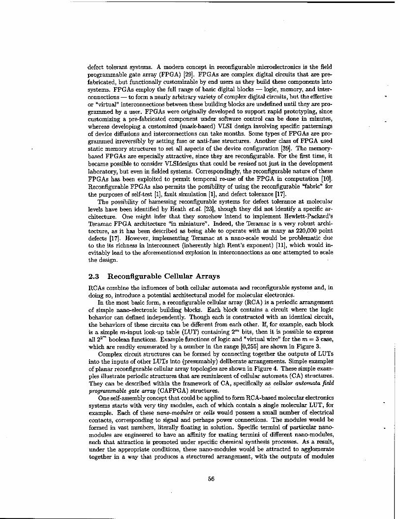
defect tolerant systems. A modern concept in reconfigurable microelectronics is the field programmable gate array (FPGA) [29]. FPGAs are complex digital circuits that are pre- fabricated, but functionally customizable by end users as they build these components into systems. FPGAs employ the full range of basic digital blocks — logic, memory, and inter- connections — to form a nearly arbitrary variety of complex digital circuits, but the effective or "virtual" interconnections between these building blocks are undefined until they are pro- grammed by a user. FPGAs were originally developed to support rapid prototyping, since customizing a pre-fabricated component under software control can be done in minutes, whereas developing a customized (mask-based) VLSI design involving specific patternings of device diffusions and interconnections can take months. Some types of FPGAs are pro- grammed irreversibly by setting fuse or anti-fuse structures. Another class of FPGA used static memory structures to set all aspects of the device configuration [39]. The memory- based FPGAs are especially attractive, since they are reconfigurable. For the first time, it became possible to consider VLSIdesigns that could be revised not just in the development laboratory, but even in fielded systems. Correspondingly, the reconfigurable nature of these FPGAs has been exploited to permit temporal re-use of the FPGA in computation [10]. Reconfigurable FPGAs also permits the possibility of using the reconfigurable "fabric" for the purposes of self-test [1], fault simulation [1], and defect tolerance [17].
The possibility of harnessing reconfigurable systems for defect tolerance at molecular levels have been identified by Heath et.al. [23], though they did not identify a specific ar- chitecture. One might infer that they somehow intend to implement Hewlett-Packard's Teramac FPGA architecture "in miniature". Indeed, the Teramac is a very robust archi- tecture, as it has been described as being able to operate with as many as 220,000 point defects [17]. However, implementing Teramac at a nano-scale would be problematic due to the its richness in interconnect (inherently high Rent's exponent) [11], which would in- evitably lead to the aforementioned explosion in interconnections as one attempted to scale the design.
2.3 Reconfigurable Cellular Arrays RCAs combine the influences of both cellular automata and reconfigurable systems and, in doing so, introduce a potential architectural model for molecular electronics.
In the most basic form, a reconfigurable cellular array (RCA) is a periodic arrangement of simple nano-electronic building blocks. Each block contains a circuit where the logic behavior can defined independently. Though each is constructed with an identical circuit, the behaviors of these circuits can be different from each other. If, for example, each block is a simple m-input look-up table (LUT) containing 2m bits, then it is possible to express all 22™ boolean functions. Example functions of logic and "virtual wire" for the m = 3 case, which are readily enumerated by a number in the range [0,255] are shown in Figure 3.
Complex circuit structures can be formed by connecting together the outputs of LUTs into the inputs of other LUTs into (presumably) deliberate arrangements. Simple examples of planar reconfigurable cellular array topologies are shown in Figure 4. These simple exam- ples illustrate periodic structures that are reminiscent of cellular automata (CA) structures. They can be described within the framework of CA, specifically as cellular automata field programmable gate array (CAFPGA) structures.
One self-assembly concept that could be applied to form RCA-based molecular electronics systems starts with very tiny modules, each of which contain a single molecular LUT, for example. Each of these nano-modules or cells would possess a small number of electrical contacts, corresponding to signal and perhaps power connections. The modules would be formed in vast numbers, literally floating in solution. Specific termini of particular nano- modules are engineered to have an affinity for mating termini of different nano-modules, such that attraction is promoted under specific chemical synthesis processes. As a result, under the appropriate conditions, these nano-modules would be attracted to agglomerate together in a way that produces a structured arrangement, with the outputs of modules
56

frwusjft
Ar
W&JS)
»Ca.b.cN A
c x
Figure 3: Example functions of three inputs, expressed within the same look-up table (LUT) structure.
Cp—O—'Cf—O—C3 Q% f\ f)
~0—v—V""^ fä*- X^\ V™V \J?'~~~\j K^ S^J, j^J
i I j ] % / \ / . Jl. Jh -,X. A ■ v-v""* r*^f -U-Q-U-V M.. A
>—u o: ö Figure 4: Example planar cellular array topologies.
57

Figure 5: Depiction of a self-assembly process resulting in a cellular nano-electronics archi- tecture, (a) Cell type I. (b) Cell type II. (c) Agglomeration of cells in solution, forming a structured arrangement through chemical self-assembly.
connecting automatically to the inputs of other modules. A particular cellular template is shown in Figure 5, involving two cell types. When combined in solution, these cells combine in a structure as shown, the basis of a complex molecular electronics architecture.
Some basic properties of RCA structures can be summarized as follows:
• Localization. Each cell connects only to a small number of nearest neighbor cells (with the possible exception of electrical power and clock connections). The coordi- nation of each cell to a small number of nearest neighbors is typical of the localization in CA approaches. Enforcing this condition ensures a low interconnection demand, consistent with the requirements of a nano-electronic architecture.
• Scale-ability. RCA structures employ cells that appear to be identical physically, and they are extensible to form structures with large numbers of cells in a periodic spatial arrangement. Ideally, they would be fabricated en masse as nano-modules that would agglomerate into ordered structures, exploiting perhaps a chemical self-assembly approach.
• Inhomogeneity. Each cell of an RCA structure can be independently programmed.
58

Figure 6: Inhomogeneity of RCA structures is enabled through the ability to configure each site from a complete basis set. In this case, the basis set is all Boolean functions of two inputs.
• Completeness. The set of elemental functions must be from a complete basis set.
The concept of site-specific functional programming is illustrated in a portion of an RCA tile shown in Figure 6. Here, each site is a LUT that can implement any single function from the complete set of two-input Boolean functions (B2) [41].
üi RCAs, digital circuits can be implemented by directly embedding equivalent Boolean descriptions into the array, configuring each site with different Boolean functions as required. As such, each RCA site or at least the RCA ensemble must establish a functional basis that is complete relative to the range of functions. The procedure of embedding target Boolean descriptions into a reconfigurable host architecture is identical to that used in static random access memory (SRAM)-based field programmable gate arrays (FPGAs) [39].
3 Problem Statement The hypothesis of the proposed effort is that RCA structures can be an effective FPGA fabric for molecular electronics architectures. A more detailed statement of the hypothesis is that: (a) RCA structures are no worse in size than traditional FPGAs (within a small con- stant factor) when viewed in terms of the resources required to express the same functions, and (b)they are consistent with the boundary conditions presently known for molecular electronics.
3.1 Description of Scope The effort will focus on: (1) defining RCA structures and the associated FPGA architecture, (2) developing and/or adapting synthesis algorithms to map arbitrary Boolean designs into these structures, and (3) establishing performance against a set of design benchmarks and comparing them to at least one standard FPGA design.
3.1.1 Identification of Candidate RCA structures
The work in this area is expected to define viable RCA templates and an overall FPGA architecture based on the RCA tile. Figure 7 illustrates the implementation of the same combinational Boolean circuit on three different RCA templates. Besides establishing viable templates, this effort would identify all of the basic mechanisms necessary to implement an implementation of an FPGA assuming the existence of fundamental building blocks.
59

Figure 7: Implementation of 4-input majority gate function(true if more than two inputs are true) with three different (feedforward) RCA templates.
3.1.2 Development of Algorithms for Synthesis with RCAs
The work in this area would focus on developing tools to map Boolean descriptions (com- binational and sequential) into RCA structures to support RCA simulation and synthesis performance assessment. Implementing complex circuits within FPGAs involves a number of computer-aided design (CAD) tools that employ heuristics similar to those used in VLSI. RCA architectures as FPGAs present special challenges and may require new algorithms , but they may have advantages over traditional FPGAs.
3.1.3 Analysis of RCA Mapping Performance
The primary purpose of FPGAs is to emulate other designs, so the work in this area will attempt to measure how well an RCA-based FPGA can perform this task. Since nearly every step in the synthesis of a design into an FPGA implementation is NP complete [10], it is not strictly possible to achieve or prove that a particular design is optimally implemented within an FPGA (in terms of area or size for example). Hence, it will be necessary to resort to more empirical means. As such, research in FPGA architectures and associated synthesis algorithms resort to benchmarks, each representing a different user design example. For synthesis, previous work has exploited a group of benchmarks developed by MCNC [15] for evaluating the performance of logic synthesis algorithms. The benchmarks will be a useful baseline, but may require augmentation or restriction to investigate particular aspects of RCA mapping performance. For a reference comparison, it will be necessary to consider implementing the same benchmarks on an alternate FPGA architecture, so that a relative quality of implementation can be ascertained.
4 Approach
This section addresses the approach to be used in the dissertation to address the three focus areas cited in the problem statement. A proposed schedule is provided in Appendix A, and a list of required resources is supplied in Appendix B.
60

4.1 Candidate RCA structures The research approach for identifying RCA architectures will be predominately based on design and analysis. Only planar tiles will be emphasized in this research, but they are not the only possibilities. This investigation will, however, address a taxonomy of architectural possibilities for purposes of context. This taxonomy will define template types and arrange- ments. Besides tiles, for example, other possible cell site arrangements include cylindrical, spaghetti, and the "wadded sheet".
In the tesselation of sites to form a tile, questions to be addressed include: (1) neighbor- hood configuration; (2) basis function set at site locations; (3) extent of each tile (number of sites); and (4) boundary configuration of tiles. Decisions in tile configurations will drive how combinational logic and sequential logic structures will be formed. One possibility is that tiles do not contain sequential logic structures. In this case, entire tiles might function as reconfigurable combinational logic structures, and sequential structures could be intro- duced at tile edges. Other possibilities include embedding sequential structures within each site. In either case, a number of physical electrical connections, comprising input/output (I/O), must be supported. The way that I/O are introduced impose additional boundary conditions.
1. General connective approaches. This portion of the research amounts to a survey. Here, structured ("crystal-like"), semi-structured ("poly-crystaline-like"), and random arrangement ("amorphous") approaches for building blocks in an RCA are examined. Even as the structured, localized templates are the emphasis for the proposed work, it is important to define a larger space of possibilities. It may well be that unstruc- tured or partially-structured approaches are more realistically approximate of tem- plates that could be manufactured in molecular schemes. Furthermore, as small-world networks [40] define a different network topology than the purely localized topologies of periodic lattices, they may be more efficient in implementing some types of Boolean designs. Unstructured approaches, however, are expected to carry some significant challenges along with them, such as establishing approaches to rapidly identify, test, and program the many individual sites.
Questions to be addressed:
• What guidelines can be formulated for selected generic RCA approaches?
2. Combinational logic structures. This portion of the work will attempt to theoretically / empirically establish which of many possible templates will make the most effective RCA tiles. The tiles can be directed or un-directed, based on cells/sites/templates with a small and usually identical number of inputs and outputs.
Questions to be addressed:
• What homogeneous / heterogeneous tile configurations are possible? Practical?
• What dimension of tile (number of rows and columns) is best?
3. Sequential logic structures. The canonical representation of a general digital system is shown in Figure 8. The model shows registration and feedback of certain sig- nals through flip-flop (registers)that are assumed to be synchronized. This portion of the work will examine strategies for incorporating sequential storage. Two basic approaches exist. The first approach involves embedding storage within the cell sites individually. The second approach involves forming other dedicated cells for storage, which would be attached at the edge of tiles. These intercalation structures would serve as an interface between tiles.
Questions to be addressed:
• Should registration structures be used (implies synchronous logic)?
61

Figure 8: Generalized representation of synchronous (clocked-mode) sequential digital sys- tem.
*«8ffi» -of Moatta»*
"WMd COM»*
Figure 9: Illustration of "light cone" propagation constraints, resulting in "dead zones" at input/output terminals.
• How should they be embedded in the overall RCA architecture (embedded within each tile, embedded periodically, or embedded in edge structures)?
• Are alternate sequential approaches (asynchronous) practical?
• If synchronous circuits are implemented, how many clocks are used and how is clock distribution handled?
4. Input / output terminal structures. This portion of the work will establish the bound- ary conditions governing the coupling of electrical signals in and out the RCA archi- tecture. An example of the constraints that arise from RCA tiles is shown in Figure 9, which depicts the "cone of influence" limitations imposed by localization effects.
Questions to be addressed:
• What terminal distribution schemes are possible?
• How densely can termini be arranged?
• Does the "cone of influence" present problems (e.g., "dead zones") in practical configurations?
5. Configuration support. This portion of the work will pursue approaches for configuring large RCA structures, based on the assumption that each site in an RCA employs a shift register, which is accessed through dedicated terminals. The dedicated terminals on each site form a second network, dedicated to configuration, in which the shift register of one site feeds into the shift register of its neighbor. This chaining is repeated across the entire array, so that in essence the RCA structure can be programmed with a single binary string. An example configuration depicting a connection of sites based
62

Figure 10: Illustration of how a planar array of sites can be configured by a single con- figuration bitstream chain, which pre-supposes that the cells are based on shift register memories.
on shift registers is shown in Figure 10. In FPGAs, this string is referred to as a configuration bitstream.
Implementing the configuration bitstream in RCA structures, particularly those im- plemented at the molecular level, is challenged by presence of defects. Without special precautions, if a single configuration bitstream were used to program a very large RCA structure, a device would be rendered ineffective by any defective device in the chain. Instead, it is necessary to consider a set of techniques that will make the configuration process more robust to point defects in the scan chain, such as redundancy of configu- ration structures and bypass switches within individual sites and employing a number of scan chains. The latter approach has the added benefit of accelerating the entire configuration process.
Questions to be addressed:
• What auxilliary structures are needed to support configuration?
• What schemes should be exploited to optimize robustness?
4.2 Algorithms for Synthesis with RCAs
This segment of research will develop and/or adapt computer-aided design (CAD) tools for RCA-based FPGAs. The emphasis of this research will be to first establish an initial framework capable of producing even crude results. Most of the research effort, however, will be concerned with investigating ways to improve this rudimentary framework to exploit more directly the advantages of RCA-based architectures, including:
• periodic arrangement (for at least the "crystal-like" tiles)leading to potential transla- tion invariant implementations for some functions
• possibility of exploiting the cellular automata basis of designs to implement more efficient synthesis
• incorporation of features necessary to handle defect tolerance
• the interchangeability for cells to implement logic and routing functions
Part of the design process flow for FPGA-based design is shown in Figure 11. These initial steps of design are more or less the same for standard FPGAs and for FPGAs based on RCA structures:
63

Boolean design description
Optimization/ Logic
decomposition Partition
Figure 11: Part of computer-aided design (CAD) flow process for Field Programmable Gate Array (FPGA) devices.
1. Design Description. An entire complex digital design is developed through schematic capture, description in high-level design language, timing diagrams, or a combination of these. The complex designs are usually expressed hierarchically and modularly, especially for very large designs.
2. Decomposition algorithms for RCA architectures. Complex functions are described hierarchically, not expressed at a level of granularity adequate for direct implementa- tion using basic building blocks. Logic decomposition, therefore, performs an initial flattening of the hierarchical input description into many simple elements, usually two-input gates. Optimizations are also performed at this design phase to minimize circuit size (number of elements). Fortunately, a rich base of research exists for FPGA CAD [16, 18], including useful tools that can be readily exploited such as Berkeley's SIS tools [36]. It is important to understand that such tools attempt to find optimal representations in terms of size or speed (depth), but optimality cannot be guaranteed, since the associated problems are NP complete.
3. Partition algorithms for RCA architectures. In designs involving more than one tile, it is necessary to parse the representation of a complex into portions, each of which can be accommodated within a single tile. More generally, if a hierarchy is involved, then partition algorithms must work at a given level of hierarchy to perform segmentations of designs to produce partitions capable of being implemented with the type and quan- tity of resources within that hierarchy level. Partition algorithms have been extensively explored for VLSI in general and FPGAs in particular, starting with Kernigan-Lin [24]. Most modern approaches involve some variation of Fidducia-Matheseys [19]. It ap- pears that the RCA architecture does not introduce any fundamental difference to how partitioning should be done, other than the immense scale expected in future molec- ular architectures. As such, it is expected that existing algorithms can be directly adapted as required.
4. Technology mapping for RCA structures. Technology mapping denotes the step in Boolean synthesis which directly correlates a desired design partition with a specific FPGA technology. Technology mapping itself is a process that includes a number of
64

Steps. One of the first steps involves logic re-packing. For example, if an FPGA is based on 4-input look up table (LUT) building blocks, then the previously flattened logic is re-packed into a number of 4-input LUTs. This process is still abstract in the sense that while compatible with a particular FPGA technology, the descriptions do not bind to a particular set of resources in the FPGA devices. A technology mapper might specify that, for example, seven, 3-input LUTs are required to implement a function, but it would not specify which of the many 3-input LUTs contained in a target FPGA shall actually be used. This initial step is illustrated in Figure 11. Up through this step, much of the CAD process is common to all types of FPGAs.
Subsequent steps in technology are concerned with mapping logic blocks to particular blocks in an actual FPGA architecture, forming the interconnections between the blocks, and establishing connection to input/output terminals of the overall circuit. Constraints can be imposed in design, such as forced resource designation (e.g., the use of specified I/O terminals) or timing constraints. In technology mapping, RCA structures are different from other types of FPGAs due to the non-distinctiveness of routing and logic, which may require new heuristics.
• Placement. This step performs the designation of specific logic resources in a target FPGA to implement the Boolean functions in a partition of a larger cir- cuit. It often works in conjunction with some coarse knowledge of global routing constraints, since in traditional FPGAs full logic resource utilization in one area of a design may over-tax routing resources, forcing a more sparse distribution (LUT depopulation) to more completely balance routing utilization.
• Routing. Complex systems involve usually at least two levels of routing: global and detailed. Global routing, as described, serves to guide logic placement, whereas detailed routing involves specific path specifications between the ter- minals of the complete wiring net-list.
RCAs differ fundamentally from traditional FPGAs in that they do not have dedicated routing resources, but rather implement routing functions using LUTs. It is simple enough to use LUTs as virtual wires, since a wire is simply a non-inverted function of a single Boolean input. The use of LUTs however for both logic computation and wiring tightly couples the normally separate heuristics used in FPGA behavioral synthesis. It is now necessary to consider the processes of logic decomposition, technology mapping, placement, and routing in more integrated treatments to obtain efficient results.
Figure 12 illustrates a simple example of how a typical logic circuit is synthesized into a 3-input (3LUT), 3-output (single-function) RCA template. A logic circuit in Figure 12a is first converted through decomposition into an abstract, equivalent representation of 3LUTs. The processes of technology mapping/placement directs the abstract 3LUT form into specific sites. The placement is non-unique and in fact is translation invariant over a limited region (referred to as the "cone of influence" or "light cone" in CA terminology [28]). This example highlights special features of the RCA:
• Clearly, in some cases a LUT acts as a wire, but in other cases it performs computation.
• Virtual wires are furthermore directional, which can complicate routing heuristics based on non-directed graphs.
• Translational invariance might be advantageously exploited in new algorithms.
• Cellular automata approaches could be directly mapped in RCA hardware as a possible alternate to ad hoc VLSI approaches in certain cases.
The special features of RCA structures suggest the possibility of combined heuristics, in which for example placement and routing are combined in a single algorithm. A recent exploration involving neural networks is summarized as an illustrative example.
65

(a)
DXlXL
-s Mini,,,», ["*" ?5
A B
(b) C D * B C D
Figure 12: Process of mapping Boolean circuit into RCA.
Neural network modeling as a combined synthesis heuristic. For at least simple problems, some intriguing possibilities exist for training-based heuristics, in which an RCA structure is modeled as a neural network. In this case, all aspects of a combinational network synthesis problem are reduced to training a representative, equivalent neural network using functional truth tables as training/testing samples. The approach of using neural networks to model combinational RCA networks is simple in principle. The most important step is in finding a neural network model capable of representing an individual site. Based on recent work on analyzing the Vapnik-Chervonenkis dimension of simple perceptron networks, it can be shown that a fc-input Boolean LUT can be represented with a single hidden layer of A; neurons, as shown in Figure 13. From here, it is possible in the case of feedforward RCA networks to simply substitute each site with this perceptron subnetwork to form a complete neural network, fully equivalent in expressive capacity. More importantly, the network can be trained using traditional methods, such as the well-known back-propagation algorithm. To examine the viability of this approach, a simple RCA network shown in Figure 14 was modeled by a corresponding neural network. This neural network was trained to design a two-input multiplier, as shown in Figure 14c. That the approach works at all is intriguing, though the design results are certainly not spectacular. As is often the case in modern VLSI design, however, often any result that works is sufficient. Furthermore, it is a simple matter to devise algorithms that could post-process a neural network result to eliminate obviously spurious portions of a design.
Tool Mechanics. In order to exploit multiple approaches/heuristics, it will be necessary to set up a common framework under which candidate algorithms can be invoked selectively. Another important goal of tools developed for RCA structures is flexibility, so that a number of different candidates might be explored.
4.3 Benchmarking RCA Performance
The work in this area involves the empirical processes of developing and applying a set of test designs as a benchmark set against prospective RCA architectures for comparison against ä reference (non-RCA) architecture.
1. Development of benchmark set. The most common benchmarks used in pedagogical studies are the MCNC benchmarks [15]. These benchmarks are designed to stress different types of synthesis approaches and offer a useful basis for comparison. It
66
Figure 13: A binary look-up table and an equivalent perceptron network.
■ %t .^.v ^ _%., ß
8 & B B & Bv B' B B 0
V h * :& 4 w Ijf ||!r §jl Wt w?
*P *(»? IS* **^ n§Kr
.sp. ?R '™ v?F
ip- w w w 4 * * * ft
0»)
Figure 14: Boolean synthesis on RCA tiles using neural networks, (a) Example RCA tile, with each site containing a look-up table, (b) Equivalent neural network, (c) Results for design of a 2-bit binary multiplier.
67

will be desirable to augment these benchmarks with other test designs, such as the sequence of complete Boolean functions of n variables, sequence of increasing complex adders, multipliers, parity functions, majority gates, etc.
2. Identification of target and reference FPGA architectures. A traditional FPGA (e.g., Xilinx, Altera) will be compared to RCA based counterparts of a similar capacity.
3. Benchmark experimentation and analysis. The research approach for ultimately an- swering the question on how FPGAs compare is largely based on empirical trials in synthesizing benchmarks on candidate FPGA architectures. The important question to be addressed is: Are there systematic trends in the divergence of size in solution circuits as the size of the starting description increases?
5 Assumptions
The RCA as an FPGA, even abstracted away from any specific VLSI or nano-scale embod- iment, is a rich exploration area. The RCA in molecular embodiments can exploit three spatial dimensions, but the proposed effort will be limited to planar implementations. The emphasis of this research effort will furthermore be on combinational circuits, though se- quential circuits will also be explored. A VLSI version could be constructed, and VLSI implementations may be studied in part to highlight sizing and/or performance issues, but this research effort does not plan to carry forward a completed VLSI implementation.
Other assumptions are delineated:
• This effort utilizes assumptions consistent with molecular electronics approaches, but does not address the problems associated with any particular scheme.
• This effort will concentrate on combinational designs, although extension to syn- chronous digital design will be pursued. The effort does not plan to develop tools for complex asynchronous digital design, which is still largely an open research prob- lem in the general sense for VLSI design.
• This effort will discuss templates in 1, 2, or 3 spatial dimensions, but in-depth work will be limited to planar templates.
• This effort can be abstract to alternate embodiments, including CMOS implementa- tions.
• Propagation delay metrics are assessed generically, in terms of LUT delay and any associated "plumbing" in accessory structures.
References
[1] M. Abramovici and P. Menon. Fault simulation on reconfigurable hardware, in pro- ceedings of IEEE Symposium on FPGAs for Custom Computing Machines, April 16-18 1997. Napa Valley, CA.
[2] Semiconductor Industry Association. The international technology roadmap for semi- conductors, June 28 1997.
[3] H.B. Bakoglu. Circuits, Interconnections, and Packaging for VLSI. Addison-Wesley, Reading, MA, 1990.
[4] S. Bhatt and F.T. Leighton. A framework for solving VLSI graph layout problems. Journal of Computer and System Sciences, 28:300-343,1984.
68

[5] M Biafore. Cellular automata for nanometer-scale computation. Physica D, 70(4):415, 1994.
[6] Carter. The molecular device computer: Point of departure for large scale cellular automata. Physica D, 10:175-184,1984.
[7] Anthony Cataldo. CMOS scaling to hit a wall by 2004, IBM says. EE Times, 1066, June 21 1999.
. [8] Chips nearing smallness limit, June 28 1999.
[9] Dale L. Critchlow. MOSFET scaling - the driver of VLSI technology. Proceedings of the IEEE, 87(4):659-667, April 1999.
[10] Andre DeHon. Reconfigurable architectures for general-purpose computing. Technical Report AI Technical Report 1586, MIT Artificial Intelligence Laboratory, Cambridge, MA, October 1996.
[11] Andre DeHon. Balancing interconnect and computation in a reconfigurable computing array (or, why you don't really want 100% LUT utilization). In Proceedings of the International Symposium on Field Programmable Gate Arrays, pages 125-134, February 1999.
[12] Ted Denlin. Presentation to SEMATECH, Spring 1999.
[13] W.E. Donath. Placement and average interconnection lengths of computer logic. IEEE Transactions on Circuits and Systems, CAS-26(4):272-277,1979.
[14] David Goldhaber-Gordon et.al. Overview of nanoelectronic devices. Technical Report MP97W0000136, MITRE Corporation, McLean, VA, April 1997.
[15] E.M. Sentovich et.al. Sequential circuit design using synthesis and optimization. Pro- ceedings of IEEE International Conference on Computer Design, October 1992.
[16] R. Murgai et.al. Improved logic synthesis algorithms for table look-up architectures. Proceedings of IEEE International Conference on Computer-Aided Design, November 1991.
[17] W. Bruce Culbertson et.al. Defect tolerance on the teramac computer. In IEEE Sym- posium on FPGAs for Custom Computing Machines, April 16-18 1997. Napa Valley, CA.
[18] Yung-Te Lai et.al. Obdd-based function decomposition: Algorithms and implementa- tion. IEEE Transactions on Computer-Aided Design of Integrated Circuits and Systems, 15(8), August 1996.
[19] CM. Fiduccia and R.M. Mattheyes. A linear-time heuristic for improved network partitions. Design Automation Conference, pages 241-247, 1982.
[20] Hans-Werner Fink and Christian Schonenberger. Electrical conductions through DNA molecules. Nature, 398:407-410, 3 April 1999.
[21] G. George and J.P. Krusius. Performance, wireability, and cooling tradeoffs for planar and 3-d packaging architectures. IEEE Transactions on Components, Packaging, and Manufacturing Technology - Part B, 18(2):339-345, May 1995.
[22] A. Gin and S. Williams et.al. Hierarchical design of quantum-dot cellular automata devices. Journal of Applied Physics, 85(7):3713-20,1999.
69

[23] J.R. Heath, P.J. Kuekes, G.S. SNider, and R.S. Williams. A defect-tolerant computer architecture: Opportunities for nanotechnology. Science, 280:1716-1721,1998. 12 June 1998.
[24] B.W. Kernighan and S. Lin. An efficient heuristic procedure for partitioning of electrical circuits. Bell Systems Technical Journal, 49(2):291-307, February 1970.
[25] David Lammers and Robert Ristelhueber. Sia road map charts wild ride. Electrical Engineering Times, 1088:1, 126, 128, November 22 1999.
[26] Craig S Lent, Douglas Tougaw, and Wolfgang Porod. Bistable saturation in coupled quantum dots for quantum cellular automata. Applied physics Letters, 62(7), 1993.
[27] James Lyke. Space electronics packaging research and engineering. In Henry Helvajian, editor, Microengineering Aerospace Systems, chapter 8, pages 259-346. AIAA Press, 1999.
[28] Chris Moore. Lecture notes, Spring 2000.
[29] John V. Oldfield and Richard C. Dorf. Field Programmable Gate Arrays: Reconfigurable Logic for Rapid Prototyping and Implementation of Digital Systems. John Wiley & Sons, Inc., 1995.
[30] Wolfgang Porod. Quantum dot devices and quantum cellular automata. J. Franklin Institute, 334B(5/6):1147-1175,1997.
[31] M.A. Ratner and A.Aviram. Molecular rectifiers. Chemical Physics Letters, 29:277-283, 1974.
[32] M.A. Reed, C. Zhou, C.J. Muller, T.P. Burin, and J.M Tour. Conductance of a molec- ular junction. Science, 278:252-254, 1997.
[33] Mark A. Reed. Molecular-scale electronics. Proceedings of the IEEE, 87(4):652-658, April 1999.
[34] K. Steiglitz S. Kugelmass, R. Squier. Performance of VLSI engines for lattice compu- tations. Complex Systems, 1(1987) :939-965,1987.
[35] D.C. Schmidt. Circuit pack parameter estimation using rent's rule. IEEE Transac- tions on Computer-Aided Design of Integrated Circuits and Systems, CAD-1(4):186- 192, 1982.
[36] Ellen M. Sentovich, Kanwar J. Singh, Luciano Lavagno, Cho Moon, Rajeev Murgai, Alexander Saldanha, Hamid Savoj, Paul R. Stephan, Robert K. Brayton, and Alberto Sangiovanni-Vincentelli. SIS: A system for sequential synthesis. Technical Report Memorandum No. UCB/ERL M92/41, Electronics Research Laboratory, Department of Electrical Engineering and Computer Science, University of California, Berkeley CA 94720, May 1992.
[37] Michael John Sebastian Smith. Application-Specific Integrated Circuits. Addision- Wesley, Reading, MA, 1997.
[38] Tommaso Toffoli and Norman Margolus. Programmable matter: Concepts and realiza- tion. Physica D, 47(1991)=263-272,1991.
[39] S. Trimberger. A reprogrammable gate array and applications. Proceedings of the IEEE, pages 1030-1041, July 1993.
[40] D. Watts and S. Strogatz. Collective dynamics of 'Small-World' networks. Nature, 393(6684):440-442,1998.
70

[41] Ingo Wegener. The complexity of Boolean functions. John Wiley and Sons, 1987.
[42] N. Weste and K. Estraghian. Prinicples of CMOS Design. Addison-Wesley, Reading, MA, 1985.
[43] S. Wolfram. Statistical mechanics of cellular automata. Reviews of Modern Physics, 55:601-644, 1983.
71

PROGRESS REPORT INPUTS ON MOLECULAR ELECTRONICS ARCHITECTURES James Lyke April 00 for the DARPA/DSO Moletronics Program
This report section outlines the third update of the AFRL effort to establish an architecture capable of scaling towards a molecular implementation. The approach exploits cellular automata concept to produce a defect tolerant fabric capable of unusual computation. In this period of performance (January - April), we focussed on a number of design issues associated with the architecture previously described. We expose issues in some conventional approaches to circuit routing that are easily remedied through improved algorithms. More exciting we describe a novel approach to design involving a neural net model of the basic molecular electronics architecture. We also define a prototype design that can be fabricated using a combination of advanced silicon integrated circuit (IC) and 3-D packaging technologies. Though not a true molecular design, this proposed prototype serves as a "dress rehearsal" of a gigascale (more than one billion logic gate) system that could be built as a single molecular integrated circuit.
This text accompanies a PowerPoint briefing on the gigascale architecture and heuristics. Its expose re-summarizes some results of the previous reports, as the briefing is intended to stand alone.
Slide 1 Update on CelhilarAutomata-based Gigascale Electronic Architectures
Jim Lyke, Air Force Research Laboratory
Fif.47
Most of the impetus of the $150B microelectronics industry is focussed on harnessing the potential of and continuing the improvement of the MOSFET. While most research focusses on driving MOSFETs towards the limits of physical realization, a few researchers are attempting to breakthrough into a domain of density and capability a million-fold beyond the best silicon processes.
This presentation deals with the field of molecular electronics, in particular with the special challenges of harnessing it in the form of architectures.
This chart illustrates the molecular architecture template originally proposed (right) and a form of paper-thin circuit packaging (left) developed through independently funded AFRL research. Such an approach allows for thin electronic planes of silicon-based circuits to be formed, interconnected, and stacked to form a dense electronic block. It is possible through the combination of many circuit layers, each of which contain a checkerboard arrangement of advanced integrated circuits, to form a very large scale system with a 100M - 1,000M gate equivalent form. Such a system, if built would employ a great number of conventional ICs to implement the equivalent function a single, small molecular integrated circuit, based on the reconfigable cellular array (RCA) architecture which has come to form the heard of the current AFRL architecture concept.
72

Slide 2 Outline
Future of CMOS and architectures
Architectural emphasis - Cellular automata basis for scale-ability - Correspondence to computer
architectures - Molecular building block approach
Near-term Research Plan - Proposed architecture - Exploiting three-dimensional packaging
- Heuristic Development
Before we attempt to address the architectural foundations of molecular electronics, it is important to address why we need to consider them. Moore's law provides an obvious roadmap and motivational basis. We briefly discuss the challenges of today's microelectronics, for some of these impact all future architectures.
Next, we will deal with the central issue of architectures in molecular electronics. We introduce a cellular automata basis as for this work and ascribe its correspondence to the whole of combinatorial digital systems. We show these to be a plausible basis for molecular approaches that exploit a self-assembly paradigm.
Then we address the elements of proposed research. The research can be divided into the abstractions of architectures for nanoscale media and heuristic investigations to leverage cellular automata and VLSI electronic bases for design. In both cases, we are concerned with the expressive range of cellular forms of reconfigurable architectures, especially as they impact design approaches as we know them today.
Slide 3 Molecular Electronics Architectures
Moore's law defines technology-driven society
Motivation: Life beyond CMOS - Scaling wall Is imminent.timing uncertain (2004-2012)
- Molecular concepts for denser than current CMOS
• 1,000.000 times smaller area
■ Extensibility to 3-D implies an additional 1,000,000-fold density improvement per unit volume
Molecular electronics (molecular=individual
device) can provide Moore's law scaling to 2050
CMOS is expected to reach a scaling limit in the near future, though no one can seem to definitely say when the we will hit the "wall". Industry marches to the wall, maybe convinced that it really isn't there. After all, such walls were predicted before but they always seemed to give way. Molecular electronics concepts promise to beat our current notions of limits in even the most aggressive CMOS technologies. When three- dimensional approaches are factored in, we are talking a potential twelve orders of magnitude compared to present-day CMOS. Based on the present assumptions, molecular electronics will allow Moore's law scaling to the year 2050. We cannot hope to convey in short a talk, much less this slide, an adequate implication of the impact that simply meeting a Moore's curve will have on aerospace systems in the future, but it has been remarked that the equivalent computation of a human brain could be realized as a single chip in the year 2020, a legion of human brains by the year 2030, and one billion human brains on a single chip by the year 2060. Intelligence will be so embedded and ubiquitous as to defy simple descriptions. Some have suggested that human intelligence itself will have to be artificially augmented simply to maintain parity within the next 40 years. We cannot afford to ignore these implications, despite how outlandish they may sound today.
73

Slide 4
Tliiophei ethyla
Pyridine
(Qonnector (D)oiior K<lectron hage (AJcceptor
A typical D-C-A organic system built from Tniophcne-etfaylene-pyridine moieties
A number of elemental approaches to molecular electronics are being pursued under the Molectronics program. In the conductance modulation approach molecular devices mimic the macroscopic devices built in bulk silicon. The figure illustrates a basic donor- bridge-acceptor "design molecular" which is analogous to a semiconductor pn junction.
Slide 5 Example Chain Molecule Implementation
of AND-OR gate
\ HI -vn-wn ,rfr
_«>+0-9"»£»*U WJ
£\-r-
•Molecular component and wire development
•'designer molecule" approach
- conductance modulation * proper I iesd energy
level« controlled throuoh selection of BpproprioTe Tuncnonai groups
- oxldetion/reductien for electron transfer
Fi».sl
The pn junction molecules can be theoretically extended to a monotonic logic (AND/OR) system, essentially equivalent to a diode logic. This figure extracted from the original proposal (need to get a better picture), suggests a molecular logic function f = a • b + c.
Slide 6 Molecular Electronics: More than
devices ■ How do you harness 10'9 simple devices?
- Design capture, synthesis, verification ■ How do you wire them together? ■ How do you assemble and package them? • How do you test finished devices? • How do you address yield issues? • How do you rectify design errors in
"gigascale" designs?
A single molecular logic function, however, does not alone from a viable electronics architecture, as many basic questions must be addressed. As random agglomerations of molecular gates will not likely produce a useful system, it is clear that some structure must be imposed upon individual devices to produce an arrangement that can be harnessed in some general fashion to create complex designs. The problem is exacerbated by the sheer scale of a potential molecular system. At the scale of 1018 devices (about 200M devices for each person on the planet), it is difficult to conceptualize the motions of, for example, schematic capture. More complex is, of course, translating the design into a legitimate implementation. Design verification can be equally difficult. In fact, the computation resources for any problem at the n = 1018 scale will may appear intractable if its time complexity functions is worse than quasi-linear 0(1018). Even algorithms that are quadratic the next lowest polynomial order will seem intractable on a machine one billion times more powerful than a Pentium. Translation of molecular devices termini for external access and an effective packaging and assembly approach are not addressed by looking at only building blocks. Testing finished devices for their conformation to the intended design is potentially as difficult as "ordinary" design
74

verification (for example, automatic test pattern generation is NP- complete). Yield, on the scale of molecular devices, cannot be perfect, and may well be worse in a relative sense than that for traditional silicon ICs. Defect tolerance must be "institutionalized" into molecular versions of integrated circuit designs. Unfortunately, even if these barriers are overcome, design bugs are likely to exist in even the most thoroughly conceptualized designs. If Windows 2000, with its tens of millions of lines of source code, is not the expression of perfection upon its initial release, how can we expect a similar feat from a chip containing a billion-fold increase in logic functions? The provisions for design rectification in hardware are analogous to bug/fix releases in software, and must also be institutionalized in the design of molecular electronic systems?
Slide 7 Research Plan
Near-term plan (0-5 years) - Fundamental issues in architectures
• Architecture fonwiatians based on CA Menpletej'
• rerfuruwee boundeiQ • lulei mmectivity coneldergtioM
- Fabrication of VLSI-based test devices
- Heuristic Development • Incriicatians of orehHecture 1» behavioral eynthesis
Far-term plan (5-20 years) - Molecular electronics
The research roadmap we consider is loosely defined in terms of near term and far term plans. The near term considers the underpinnings of architecture and provides guidance to molecular electronics developers (i.e., DARPA Moletronics team members). It is possible to consider more concrete demonstrations of gigascale architecture that can be developed to illuminate the challenges and potential of Moletronics through "ordinary" VLSI implementations (though, not that ordinary). This sort of testbed makes it possible to focus more abstract architectures and features (i.e., defect, assembly tolerance) and may well uncover additional second and third order effects that might go unnoticed. If the near term plan can identify full, realistic architecture templates in detail, establish software tools, and converge on at least one molecular approach, then it is all the more realistic to expect that a molecular electronics solutions will emerge in time with enough overlap to the SIA roadmap to make Moletronics a serious contender for a CMOS replacement.
Slide 8 Strategies/Challenges for Nanoscale Electronic
Architectures
Low interconnection supply
- limited number of wires can converge in a given location
Effective lithographic approaches or alternatives
Defect tolerance
In this effort we are centrally interested in the role of architectures in nanoscale systems. Here, we see three central challenges....
75

Slide 9 Implications of dimensionality on interConnectivity
f _•
I b+H I I i
3-D (no crossovers) 2-D (crossovers required)
The trends of dimensionality are illustrated somewhat in the simple figure. In it, a graph representing a 3-D design is flattened into a 2-D implementation. In the implementation, identically sized square modules are used, and it is clear that not only are crossovers induced, which require additional interconnect layers, but some interconnections must be longer than others due to packing considerations. On the other hand, a 3-D implementation of the same graph would not require crossovers and would have a shorter minimum average interconnection length.
Another problem in design which complicates interconnect is the notion of hierarchy. At any given level in design hierarchy, a black box is usually formed as an interconnection of several black sub- boxes. At each successive level in a hierarchical design, the current set of interconnections (literally in some cases) is built on top of interconnections defined at lower levels. More complex designs have more hierarchical levels, which leads to interconnection growth. Silicon gate arrays devoted otherwise useable silicon resources to channels for interconnect, and the interconnect resources are always heavily competed for in large-scale designs.
Interconnection sprawl is in part gauged by growth in terminal count, as codified in Rents' rule, which describes pincount as a power law relationship to the number of building blocks in a complex circuit. Molecular architectures may need to discover a way to "tune" the Rents' rule relationship, which is a concept that makes some sense in the proposed architectures.
Slide 10 How Dimensionality and Interconnection Demand Affects Implementation
Dimensionality - Non-planor graphs require crossovers - Flattening n-D into 2-D forces length of some
interconnections to increase
Interconnection demand (Rent's rule)
- Hierarchy requires interconnection at each level
* Ignored in design 'capture*
- Real estate competition for interconnection channels ore intensified
- Do molecular CAs implement a tune-able Rents rule? Fi.
Behind the whole issue of interconnection complexity are factors that are somewhat intuitive but more qualitative/empirical vs. quantitative/analytical. It must be clear, for example, that dimensionality plays a role in interconnection complexity. An n- dimensional cube, for example, is necessarily congested when represented in m(<n) - dimensional space. Architecture in digital design do not necessarily conform to the standard notions of 3-D spatial limitations, and interconnection complexity can suffer as a result.
76

Slide 11 Comparison of IC process trends toward
increased interconnect demand
I Sourco: Sematech
zmam%im?fi2'mmi
1.0 micron 0.1 micron
Drawn to v\m »mm* sca/a
Slide 12 A New Twist on Old Themes ' Extension of concepts in cellular automata
(CA) for molecular electronics - Exploits relationship between cellular automata
and combinational digital electronics
■ Equivalence relationship lends new insights to extension of CA approaches - Extensibility to universal computation
• Exploit reconf igurable approaches - Unique exploitation of field programmable gate
arrays permits re-use of molecular resources
• Examine implications of these approaches to modern automated design synthesis
This chart illustrates the progressive intractabilities of interconnections with scale. At 0.1 micron, it is estimated that 10 kilometers of interconnect will be needed to wire a typical IC. It is not hard to imagine what happens at circuit scales one million times denser.
Interconnections are a necessary evil when dealing with architectures, and they become more complicated with scale, as shown in this Figure. Based on the cross-section of 1.0 micron and 0.1 micron processes, it is evident that the complexity of the interconnect manifold is worse with diminished scale. This is what could be referred to as a "fact of life". It is also something that molecular electronics' designers must cope with and it could be more than they bargained for. Unfortunately, with the promise extremely tiny devices comes, the baggage of conductor-dielectric manifolds that guarantee each signal connects in a manner prescribed by architecture. Any researcher who claims they can build nano- electronics systems is only partially correct if they cannot address this issue. Consider the size of the interconnection manifold in the limit where the device size is zero. Without mitigation of interconnection, the true density of complex systems may actually be expressible as a parabolic function whose minimum occurs at a critical dimension above, not below, nano-scale.
The punch line of the our research plan in architectures is to leverage two substantial research bases, one being cellular automata, the other being digital electronics, hi this manner, a simple and direct relationship is established between CA and digital electronics. The equivalence may offer new possibilities in its own right. Certainly, it is possible to achieve universal computation in the Turing machine sense. The approach contributes a reconfigurable basis to a CA- inspired architecture, which gives rise to a straightforward attack on defect tolerance. The new architecture is encouraging in that while it can harness the existing base of computer-aided design (CAD) approaches, it offers hope that still better approaches can be found that exploit the special features of the architecture to simplify implementation and test of complex designs.
77

Slide 13 Binary Cellular Automata
Lattice of sites in 1,2, or 3 dimensions
Each point has a value of {0} OP {1} Simple computations are performed at each site at discrete time intervals Value of any particular site at next time step is explicitly a function of site values in a specific neighborhood r about that site - State transition matrix size of 2r
We introduce a few basic concepts of cellular automata (CA). CA, in this case, are points in a regular discrete space (1-D to 3-D), perhaps on a fixed grid. Each grid point has a discrete value, either "0" or "1" (binary). All points in the grid (CA structure) are updated at the same, discrete time intervals. Most importantly, the updates are based on simple, Boolean functions (rules) which depend only on the nearest-neighbor grid points. As such, CA are possibly the simplest structures capable of sustaining computation in any meaningful sense.
Slide 14 Cellular Automata: Simple devices, complex behavior
It is sometimes hard to believe that structures so simple can produce behaviors so complex. This chart illustrates an evolution of 1-D CA structure, which at any one instant is represented as a single line, like the line in a raster scan display. The picture is a spatio-temporal strip chart in which time proceeds down the page. Each new line is computed based only on values of the previous line (black = 0 and white =1).
Slide 15
dii'&l'Flil
Time evolution "strip chart' demonstrates different classes of behavioral evolution - Sinpk - Oscillatory - S«lf->Mlar - Cofflpkx, chaotic
Left examples - (n>pcr)R>jlt#45,
chaotic - (lo»er) bile #182, Mlf-
»milnrrty
This figure illustrates the evolution of a 1-D CA using different rules. The top of each figure represents a simple linear CA structure with an initial pattern, and each row represents the value of the sites at progressive time steps. By simply changing the state transition matrix, the entire behavior changes, as evidence in the figure.
78

Slide 16 Examples of CA-like
behavior
Examples of physical phenomena which correlate well with CA behavior are shown.
Slide 17 1-D CA conversion to 2-D
©
1 CAbMH 2 Logic ba*(cMwwc«on»*wm tor B only) 3. Logic baate (other cenrwettan« «town)
The original molecular architecture is based on a 2-D cellular array, converted from a 1-D CA structure. This effect is achieved by simply converting a 1-D feed forward structure. The entire 1-D (linear) CA structure is replicated into a number of rows, forming a 2-D tile. In this case, the neighborhood is the same size, but the source values are taken from the previous row.
Slide 18 Redefine CA sites as look-up tables (LUTs)
An 3-input LUT (LUT-3) is identical to a universal cellular automata of neighborhood 3
LUI3
I
CA site can be modeled by a look-up table, which directly implements the state transition matrix. In this figure, a 1-D CA with a three-neighborhood (consisting of a site and its left and right nearest neighbor) is modeled directly with a 3-imput look-up table (LUT). Since the LUT can be reconfigured the LUT can be thought as a universal CA site, capable of implementing any possible binary CA function.
79

Slide 19 Example Functions of LUTs
MAc^AOR • 4»h4-Ai
Logic functions - bifrtlylwfhi—rtiyfuncH*n>fU.wiliifuti - DMMW*M nura compkx fwcttM kit* f>
Wire - fafluMntpacf-ttH-oufhttoyrttaattwrLUTf - TradtrMl-lra-^ilBtyfw'viniMrwlrMUItr
Con also program LUTs to fgtwr» on« or all inputs
By using a look-up table (LUT) structure, it is possible to have a CA cell imitate any Boolean function of three inputs in this case. This chart shows a number of possible functions and the corresponding rule numbers. It turns out that the ability to imitate a wire is one of the most important cases, for this simulates the ability to form interconnect on demand. It is also worthwhile to note that LUTs can be programmed to ignore one or more inputs, and they can be programmed as NULL functions as well.
Slide 20 Cellular/molecular field programmable gate array (FPGA)
. 1 ■ Fixed grid in x,y of rnariy
<7\ configured to on arbitrary
@ffi^^^^^1 5*"ä) ' Each cell in o given row receives
ät-dL--' neighbors of the following row
* architecture In a 2-D physical implei Mirtotion
Fit.«
The result is the original molecular architecture. The feed forward structure is identically imposed at all site locations. The architecture can be referred to by a number of terms, including molecular FPGA, cellular FPGA, or reconfigurable cellular array (RCA). It is different from the standard notions of CAs in that: (1) it is neither "properly" a 1 -D or 2-D CA, but rather a 2-D implementation of a 1-D CA; (2) each site can be programmed distinctly.
Slide 21 Characteristics of New Approach
Periodic structure - Amenable to chemical self-assembly
Reconf igurability-Logical behavior of each cell independently and repetitively programmable after fabrication
Low interconnection demand 1 Defect tolerance
Some assertions can be directly about the molecular architecture. Some are obviously evident, others will be illustrated further. The first point is that the architecture is periodic in a simple way. Each of the LUTs would be in principle amenable to self-assembly (the LUT contents are discussed later). The LUTs are individually configured so as to produce from their ensemble a desired complex behavior reflecting the intended digital design. It should be evident that no interconnect explosion would result in a reasonable implementation of the architecture, which suggests that either: (1) the notion of architecture is somehow fundamentally altered, or (2) that the accommodations necessary to implement complex interconnections are somehow dealt with by the architecture, perhaps due to the notion of the "virtual wires". As it may be that virtual wires can be used to time the interconnect complexity reflected in a desired design, they can also be used to tune the specific way a design is located onto the LUT mesh. We suggest now and show later that this gives rise to the notion of defect tolerance.
80

Slide 22
Comparing Real-World FPGAs to Cellular FPGAs
The molecular or cellular field programmable gate array (FPGA) is now compared directly to traditional FPGAs, in part to demonstrate why the latter cannot be scaled directly to a molecular level.
Slide 23 Generic LUT-based RAM-based FPGA Unput look-up *W-(lUn
b 1
«ten
* dock
^r".. '■■"■'■'; ■ ></\j.
Fit.»
Real-world FPGAs implement the key elements of all digital design: (1) LOGIC, (2) MEMORY and (3) INTERCONNECT. By combining a look-up table with a flip-flop (upper left), the logic and memory elements are established. This structure is one of the many ways that a configuration logic block (CLB) can be implemented (upper right). Real world FPGAs use many CLBs to implement designs. On this chart, the interconnection manifold is shown as an amorphous blob that encloses the CLBs. Unlike LUTs or CLBs, the interconnection manifold often lacks the fine gram periodicity amenable to scaleable implementation. In fact, the exact structure of the interconnect manifold is empirically based, eclectic, and usually highly proprietary in its specific details.
Slide 24 Routing in Generic FPGAs
OP -^
£=; Lrtara»»«ction polk« fonoocl by »Hino W*** • Wiring be1»»en inputt ond «rtpol» of Boolean fine««» h FF6A« Of« rcduotd *> 0-1 pro«™.!*»; ilooWor» touting «Aon«« daton*» uHinot« notion flaxfcilHy of FP6A«
At least on a generic basis, real FPGAs implement programmable interconnect with irregular arrangements of physical wire and switches as shown in this figure. The specific "rhyme and reason" for the placement of wire and transistor switches is at the heart of FPGA design, which is largely empirically based and an art. If too many wires/switches are used, the silicon is poorly utilized. If too few the FPGA is incapable of wiring practical designs. FPGA designers argue amongst themselves as to whether FPGAs should be "LUT rich" or "interconnect rich", which are considered in a simplistic sense to be the two extremes. A number of FPGA architectures, including the HP Teramac, are reported as being interconnect rich.
81

Slide 25 Typical FPGA (corner of XC3020)
SjEf Jnr^Mliliirnrf= fflF" t< '"' MwydBtalt
B «
3g£ P r i^ il I'll f
so e© r=i
This figure illustrates the structural irregularity and complexity of a simple FPGA design. The example shown is from an obsolete Xilinx 3020, which is a 2,000-gate FPGA (today's state-of-the-art Xilinx FPGAs have 1,000,000 gate densities). This quadrant demonstrates that rote scaling of complex ICs would be a molecular synthesis nightmare. Clearly, any real world FPGA would require a considerable re-casting exercise to implement a molecular form. Even this simple example of an obsolete FPGA would pose a major challenge, and it is probably better to avid the attempt.
Slide 26
Slide 27
Impacts of configurability on Real Estate in Commercial FPGA
c
• A: Real estate due to logic of desired function (area=x)
• B: Plus real estate due to configuration of LUTs (area-lOx)
• C: Plus real estate due to configuration of routing (area-lOOx) ■ B
Ftf.71
Comparison of Conventional FPGAs to molecular FPGA (AAFP6A)
• Similarities
- Both use LUTs - Both are software configured with serial
bitstreams
• Differences - MFPGA has no programmable routing - MFPGA supports only nearest neighbor
connections - MFPGA has much simpler (periodic)
structure
FPGA architectures are not deliberately complex by intent, but rather by necessity. The reasons that architectures have complex interconnections has already been discussed cut this figure illustrates how interconnection complexity is manifested in FPGA architecture. The smallest of three rectangles depicts the size required by a specific complex digital design. The design, of course, contains logic, memory, and interconnect. If the normally fixed logic functions are replaced by LUTs, then the area need for reconfiguration storage for those LUTs is represented by the next largest rectangle (B), about 10X the size of the first box. Though this area represents a significant overhead, the area incurred in replacing fixed interconnect with programmable interconnect is far worse (rectangle C). This disparity illustrates interconnect growth in a different form than before, only further amplifying its critical influence on architecture. (Note: Andre DeHon, who created the original of this figure, says this must interpreted with caution. I originally thought that it implied that an FPGA requires 100X the real estate of a full custom design, but he indicates that this is not fundamentally a correct interpretation).
82

Slide 28 Equivalence (functional isomorphisms) between CA and random logic forms The molecular FPGA structure's periodicity has other obvious but
interesting properties. One of them is translation invariance. This figure illustrates a simplified design implementation. The user design (upper left) is first a re-cast in terms of LUTS through a process known as technology mapping. This process is used commonly in gate arrays to map a starting design into cell libraries for a target VLSI process. In this case the cell library is a single entity (the 3LUT). From here, the abstracted design is physically located into the tile and interconnected through the process of placement and routing. This figure demonstrates both design non- uniqueness in terms of the five "isomorphic" implementations and translation invariance in the three CA-based implementations.
Slide 29 Defect tolerance-, before and after
This implementation flexibility can be used to circumlocate around defective LUTs. This figure illustrates an implementation over a defect (left), and the resulting impact zone (dotted lines) compromises two output functions (bottom row). The defect in this case is easily "skirted" by reprogramming the LUTs in the vicinity of the defect (right), thereby recovering use of the surrounding LUTs to yield the desired functions.
Slide 30 VLSI Implementation of Cellular FPGA
3-LUTs (-100 transistors) can be implemented in high density - 200,000/cm1 In a 0.25um process
• Produces ~1M gate per 1 cm die
■ Define I/O at 25um pitch ' Define single chip designs
- generation 1: 2mm x 2mm die (~20K gate) - 6enerotion 2: lern x lern die (-1M gate)
It is possible to directly describe silicon versions of this type of architecture. The LUT is principally independent, and it could be implemented in conductance modulated molecular gates, quantum dots, and of course silicon. The silicon implementation provides a simple way to study example architectures. For example, it is possible to implement 200,000 3LUTs, each of which represent a 100-transitor module, in a 0.25 micron VLSI process. An example architecture could be implemented in two phases, using low-cost MOSIS fabrication runs (~ $lK/mm2 for 25 samples). The first pass feasibility IC would establish basic feasibility (2mm X 2mm ~ 20K gates), while the second run would build a more serious prototype (~ IM gate).
83

Slide 31 VLSI / Gate Implementations of 3-input lookup table
mi f'V f~ it
ihr
- i. F«.7T
The actual implementation of a 3LUT is straightforward in silicon or other technologies, provided that the right building blocks are available. This figure illustrates two implementations, based on pass-gate (left) and logic gate (right) approaches.
Slide 32 Completion of Cellular FPSA Architecture (Example)
b[Mt«i.y) *<* -i ii i i i i i in
mxnBMdUm
i i i i i i i i rrv nock regittarHa(btt«rey)
Creates feedback path necessary for general clock- mode sequential behavior Ft n
While the FPGA template described up to this point is an important and fundamental structure, it must be augmented in order to form a complete device by including: (1) feedback and (2) user memory. These features could be incorporated by using more sophisticated LUT arrangements, but this approach creates drawbacks that are beyond the scope of our present discussion. Rather, it is suggested that the LUT tiles be arranged and juxtaposed with other structures to achieve the desired effects. This figure illustrates a two-tile structure in which the tiles are directed in opposition. They are not directly abutted, but rather they are joined to a common articulation structure.
Slide 33 Detail of bit array between tiles
(LUT) (LUT) (LUT) r—
lt:j (un) (LUT) (LLFT) _
III j5><^C><?&><d= fe (LUT) (LUT) (LUT) _ fe# ^-t«^ J>r<L J^rC ^-*VL
(urn (LUT) (LUT) p;
_ (im) (im)
_ (im) (im) £r*-^ Jir<l J>I^ ^"*
rim) (im)
_ (im) (im) —
s.
(LUT) (LUT) (LUT) sh**^t^^^\~^~ (im) (xm)
? T T CL KK y y F«.»
This figure illustrates the specific arrangement of how the "dangling bonds" of the LUT tiles intercolate the register structures. This configuration allows for a simple scheme that is capable of implementing clocked-mode sequential designs, such as state machines.
84

Slide 34 Configuration of MFPSA
p^^V^i^V'VJffV-uuy- "© • LUT memories ">s, implemented os shift "x^H register (2-phose 5sl clock) "fun)—' ' ,>r • Multiple .-jSv-. configuration chains <5[ for large device
—»UIJM-^I^J-^IJUTV-^IUTV "v"")—
FirM
The LUT tiles are analogous to blank memories, tapes, etc., in that they cannot perform any particular function until programmed. This figure illustrates how a configuration chain can be established through a LUT tile to accomplish this programming. It pre-supposes that the LUTs are based on shift registers. The configuration chain is only an accessory system for programming, and these links are normally "invisible" with respect to the normal operation of the tile. The particular chain pattern shown is actually an obvious but very bad choice for the programming configuration, since it is vulnerable to single defects that could cripple the configuration process, rendering an entire tile useless (better configuration chains were described in the Dec. 99 report).
Slide 35 Three-pass plan to gigascale using MCMs and 3-D packaging
■ Define Multichip modules - generation 1: 2 xlorZx2die(40 or BOKsate) - generation 2: 5 x 5 (-25M)
• Exploit ultra-thin 3-D technology to stack - generation 1: 4-6 layers (160K to 480K gates) - generation 2: 5-10 layers (125« to 150« gates) - generation 3: 40 layers (-1,000«=1B gates)
As an illustrative example that is partly digressive from the singular pursuit of a molecular architecture, we outline a gigascale architecture testbed proposal. This activity represents a possible track to implement the cellular FPGA on a somewhat massive scale, but based on realistic implementations involving 0.25 micron CMOS and a paper-thin form of High Density Interconnect (HDI) multichip module (MCM) technology. In three passes, this prospective program would implement a one billion gate demonstration vehicle.
Slide 36 Patterned overlay High Density Interconnect
Employed as first-level interconnect
CAFKAchlp
:*(l»od for 3-b MCM «tack)
let (mad for 2-0 MCM«)
Mechanical «fcstivlv (will later b« around to k« t SO urn)
The MCMs in this scheme would collect together a checkerboard pattern of cellular FPGA chips, each of which itself contain a number of tiles and register-intercolation structures. In this embodiment, the ICs would be equipped with a perimeter array of input/output (I/O) "alligator clip" termini at a very aggressive pitch (one ever 25 microns). The MCM would employ a nearest-neighbor connective pattern, characteristic of the lower levels of the tile design. It is expected that these connections can be accomplished with a single metal layer (metal O).
85

Slide 37 MCMs based on cellular FPGA blocks
ffl/ ■ ■■■1
25uni
1st gen chip (2mm sq.) ■ 25 micron pitch I/O
fig
1 Each die design will contain large number of perimeter and interior I/O - lmm square divisions
throughout die to form zones
- Perimeter of each zone 25um I/O pitch
■ Die juxtaposed in MCM ■ Interconnections between
nearest-neighbor die and MCM edges in metal 0
This chart illustrates that the "alligator clip" connection is very coarse. On average, at least two LUTs will be contacted by one bond connection. Furthermore, a lot of LUTs in the perimeter zones will be missed altogether, which mimics the way that a molecular tile would be connected to the outside world. The demonstration would show the potential of the architecture to be assembly tolerant.
Slide 38 Ultra-thin High Density Interconnect • Recently demonstrated capability to thin entire
MCMs below paper thickness and retain functionality
• Silicon bends when thinned below 50um
\ ■ -•'■■£* •>">"'' *f£v'-V:.;'«V:'.:-!
The prospective VSLI implementation will ultimately mimic a 3-D embodiment of the FPGA. Achieving this will require paper-thin layers of 2-D circuitry. This chart illustrates a pre-thinned but finished MCM. A sacrificial substrate is employed, and it will later be ablated away through a back-grinding process.
The principle of a paper thin HDI was proven possible in 1998 in an independently funded demonstration through AFRL.
Slide 39
m^m,
2-D MCM fabrication ■"■ • Basic MCMs built in HDI - Rely on defect-tolerance " " " attributes of CA-based design DIVU - Allows coarse placement of vias """"" • Test individual MCMs and
capture knowledge of defect zones Back-grind tested MCAAs as an entire assembly - No handling of ultra-thin chips!
5T3^0imi
The modules in preparation for stacking are interconnected. The interconnection at this level only binds together chips within the same circuit plane. The assembly is then thinned from 1,500 micron to about 50 microns.
86

Slide 40 3-D MCM Fabrication
• Stack and process one layer at a time
■ Modules are so thin that vias can penetrate through remaining substrate
• Unprecedented I/O capabilities between 3-D levels
J
The demonstration system is based on densely stacking a number of dense circuitry planes. The novelty of this approach is based in the idea of penetrating entire MCMs with connective vias to electrically bind the layers together vertically, producing a unique 3-D interconnection approach that does not require a true 3-D-IC approach.
Slide 41 Simplified 3-D sequence for 2 layers
l'-tHOr.
Ghie 2nd substrate to first
Laminate additional layer of dielectric (becomes metal 1 of 2nd module)
"Blast" vias to metal 0 of module 2 and metal 0 of module 1 simultaneously
fm-tr
Thinned circuit planes are next stacked one-by-one. As each MCM- plane is added, an additional dielectric layer is laminated onto the emerging stock. A series of vias are formed to "stitch" each new layer to its nearest neighbor in designated points, which in effects implements a full 3-D scheme.
Slide 42 Sky = Limit
Step and repeat the 2nd layer as required Ten layer stack about one mm thick
> One hundred layer stack less than one inch thick
The process is relatively low temperature, and residual stress is balanced by the reinforcement of added layers. This figure illustrates a number of stacked layers. The only apparent limitations pertain to fixturing.
87

Slide 43 Obvious Issues
Physical packaging - Thermal management
• Could direct bond every rrfh layer to heat sink/spreader
• Seek lower power implementations
Heuristics to harness power of giga- scale capability
A VLSI implementation would expose other real world issues, such as power delivery and thermal management. The ad hoc VLSI implementation may require the insertion of heat spreaders for example. The operating frequency limit might well be thermally dictated.
Slide 44 Heuristic Investigation areas Examine extensions of traditional electronic design automation (EDA) methodologies - Partition, placement, logic decomposition,
technology mapping, routing
Special considerations - New heuristics for simultaneous technology
mopping and routing - High regularity of grid slructure may permit
algorithmic approaches for synthesis - Possibility of hybrid CA / VLSI basis
• E*pWtprobkmdo«Mhiw«ediiior«efftckntlybyCAj / VUI in localized regions
- Self-test / diagnose / capture defects for synthesis F«.W
"Heuristics" refer to approaches that produce good results on average (but not necessarily optional). We accept sub-optimality in exchange for rapid solution time. A rich body of knowledge has evolved over the last 15 years in electronic design automation (EDA). We would like to use these directly if possible on molecular architectures. Other than sheer scale, the principle has merit, but the new architecture is different from standard FPGAs. As such, allowances must be made to accommodate the unique aspects of the molecular FPGA. At the same time, we speculate that the differences might be exploited in new algorithms that actually work better for molecular FPGAs than for other FPGAs. Results are presented to bear these points out.
Self-test in the molecular FPGA has been given only scant mention, but it should be clear that self-test is actually simplified for a regular architecture. It is possible moreover to harness this architecture and its resource to accelerate self-test and fault diagnosis. By using virtual wires, pattern generation algorithms can be devised to rapidly expose defects. Based on a fault signature, a supplement test configuration can be generated to further "zero in" on particular defect regions. Such methods are reminiscent of binary search algorithms, which operate in sub-linear time. Further exposition of these algorithms remain the subject of future progress reports, in which we hope to conclusively dispel any doubt as to the veracity of these claims.
88

Slide 45 Need for Routing heuristics for CA- based FPGAs
(left) source problem (center) results (incorrect) from typical FPfeA routing tool (error node in red) (right) corrected results for cellular FP6A - PMiireJckflnHion of a nod« rasolutfen function (nod. in
yelio») "■;
The standard algorithms for routing FPGAs must be adapted slightly for molecular FPGAs, as shown in this chart. The left figure illustrates a contrived routing problem on a small LUT tile. The center figure shows a result using a simple greedy algorithm (based on Dijkstra's shortest path method). The result is unfortunately incorrect, as the highlighted node in the center figure appears to connect but in fact is a dead (not defective node). A slight "manual shove" produces a correct result (right figure) in which signals 3 and 5 intersect (such as "OR"). Such adjustments are simple in principle but uncommon in traditional tools.
Slide 46
Preliminary work on neural-net based design tools for gigascale
The remainder of this report describes preliminary work on exploiting neural nets in a new heuristic method for circuit design with molecular FPGAs
Slide 47 An n-input look-up table is adequately modeled by a perceptron network with
n neurons in its hidden layer*
i i i i i
5-LUT
* based on analysis of Vapnik-Chervonenkis dimension fi dimensionality, proved with brute force limuUtion for n - 3 c
It can, for example, be shown by combinational analysis that LUTs can be modeled with neural nets. To do this a simple perception network containing a single hidden layer is employed. The hidden layer contains the same number of neurons as the arity of the LUT being modeled, and the hidden layer is fully connected. For example, a 3 LUT uses three neurons in its hidden layer. The example shown models a 5LUT. In any case the hidden layer drives a single output neuron. To convince ourselves the approach works, we conducted brute force simulations on all 255 cases for a 3LUT and its corresponding neural network.
89

Slide 48 3LUT tile and neural network model
*?.. ^ ^ft> p ?-, --?-- .-K ,-K .-? Ejj [ju^ £wj Eü] ^ 0' ^ ^ 'gf ^ ö | § 8 19 t$T$~^j!J£ $* E 3 @ Ef S ü 4f ~jfi ^ f£ $* F 3 6 S @ 1*3 & m |& ill &
Fi».M
By simply replacing each LUT if a molecular FPGA tile, we can directly form a structured neural network capable of mimicking anything that the original network can do.
Slide 49 How to train neural nets to design circuits
Abstract a neural net model Use design input / output relationship as the training set (= test set)
• Build back-propagation system around tile
• Train / re-train with randomized version of training set until convergence occurs (if it occurs)
Given this model, the concept of training the neural net to design circuits appears to be straightforward. The process involves creating a training set based on the logic functions that are desired. This set is used in conjunction with a standard back-propagation algorithm to adjust the neuron weights. Then, the same training patterns are used to test the circuit formed. The process of training and testing are repeated until convergence occurs (or you get tired).
Slide 50 Neural network circuit designer This figure illustrates the design system implemented. Convergence is defined as a test set that produces no classification errors.
90

Slide 51 NN-produced results for 2-bit
..multiplier Designs are not optimal, but they work Could be improved with post-processing These preliminary results show feasibility in training neural nets to design circuitry for molecular architectures
A number of examples were tested, and in a nutshell the approach works. The example shown here is a neural net design of a 2-bit binary multiplier. The results are non-unique and non-optimal, but they work. This statement begs the question: "What is good enough?" In VLSI, for example, optimality is usually defined in terms of circuit size or speed. Here, since the tile size is constant, any convergent solution is the same size. Furthermore, any solution propagates through the same number of LUTs. Hence, all solutions are essentially equivalent. Still, the neural net produces very odd results, like those produced by a drunken designer. Some clearly spurious signals are produced, but they do not alter the enheuric validity of the solution. It is likely a simple exercise to post-filter the neural net solutions so as to remove non-sensical constructs. Furthermore, the use of other iterative improvement techniques (e.g., simulated annealing) could be considered if there is a benefit in doing so.
Slide 52 Summary • Molecular electronics offer a new roadmap
beyond CMOS, but raise new issues about gigascale architectures
■ CA-based architectures proposed as an approach to harness tremendous densities
■ Correspondence between cellular automata and circuitry could provide powerful new insights directly relevant to the design of future electronics systems
■ Proposed VLSI - MCM - 3D implementation can allow early investigation of super-dense computational architectures ^,
91

AFRL joins NRL's team in the supporting capacities of architecture, packaging, and interconnections. We describe a seven-level hierarchical architecture, based on modified version
. of the DARPA-sponsored AFRL Phase 1 architecture. The architecture is specially adapted to NRL's viral scaffolds. Based on properly harnessed properly configurations of these blocks, an end-to-end picture of a terascale molecular system can be developed, capable of supporting almost arbitrary digital system implementations. In this discussion, we further turn our attention to the equally significant challenges of interconnections and packaging and outline our proposed molecular chip scale package (MCSP) based on a merging of advanced transition interconnect structures.
"Outside world" micro-ball grid array
Level 7 - Macro/meso-connect
&&&&&&] .Y..XW^U>X:Y x x- i xx&frTZ&TJsm
Level 6 - Meso/micro-connect
Level 5 - Active micro-substrate /Tv^^T^.^: ^[^1^ 4 - Micro/nano-connect
Level 3 - LUT tile-complexes Level 2 -LUT tiles Level 1 - Viral nano-blocks Level 0 - Molecular electronic
Devices
Figure 1. Hierarchical architecture for NRIAFRL molecular electronics approach.
AFRL defined a basic set of architecture principles and concepts for molecular electronics in the first phase of the DARPA Moletronics program. Not surprisingly, we propose here a core architecture approach based on defect-tolerant, assembly-tolerant periodic aggregations of fundamental nano-scale building blocks, namely those scaffolded onto the viral host structures, or viral nano-blocks (VNBs). The key constraints necessary to establish a viable system are summarized and prioritized as follows:
• An electrically viable signaling system in which inputs of VNBs are compatible with outputs of other VNBs (critical);
• The availability of 8-12 terminal sites on the VNBs to serve as primary nano-modular input/output (I/O) for signal, clock, and power distribution (high);
• The ability to effect causal or polarized arrangements of VNBs to establish feed-forward networks (for example, it must be possible to avoid connecting the outputs of two VNBs together that may wish to drive incompatible signals) (high);
92

I
The ability to control to (within at least 10-15%) the number of rows and columns in a block aggregate ("tile") (high); The ability to introduce a minimum of two different engineered viral structure types, one being a logic compute type (such as a look-up table) and the other being a data
storage/buffer type (such as a D-type flip-flop) (high);
• The ability to attach to a unifying substrate which could serve as a global clock and/or power and/or signal distribution system (medium);
5^ T \&
m "* ( 2LUT ) ►
Figure 2. Reference design of two-input look-up table (2LUT) based on elemental shift-register memory cells and controllable switches. Switches are closed when Boolean variable beneath is eqal to logical 1!
AFRL will work closely with NRL to co- engineer the viral nano-blocks to establish these and other derivative properties necessary to support computational architectures. It is possible to consider two- and three-dimensional arrangements. VNBs appear more natural as 3- D building blocks, a principle we discuss later for engineering interconnection manifolds.
Confining for the moment the discussion to molecular planar assemblies , it is necessary to consider a modification of the Phase 1 cellular architecture. Here, we consider a case where two independent look-up table (LUT) structures are engineered into the same VNB. A reference two-input LUT (2LUT) is shown in Figure 2, based on a molecular memory and molecular switch. It is important to note that the 2LUT is an example of a computational block that is capable of universal digital implementations, but it is not the only one. Furthermore, the Figure 2 symbolic representation is but one of several embodiments.
The use of VNBs as a host of a dual-input 2LUT logic building block is illustrated in Figure 3. It is necessary for planar arrangements to exploit dual-2LUTs since crossovers are necessary in digital design and 2LUT structures permit the definition of a crossover as a virtual wire. Simple examination of a candidate functional implementation using a VNB-based tile demonstrates the need for crossovers in even the simplest functional mappings.
93

ft?',
VA ^ "Vy.i
W y y
\<^*Jf£^X**^
A collection of VNBs arranged in a periodic and compatible manner form a tile. If the molecular scaffold of a VNB can be thought of as a level 1 assembly, the tile would be a level 2 assembly. Such level 2 assemblies, if large enough, can compute any spatial digital function. This capability, however, is not sufficient to accommodate complex digital functions, such as finite state machines. For these reasons, it is necessary to consider a level 3 structure referred to as a tile-complex. Tüe-complexes consist of 3 Mapping elemental computation two or more tiles m which loop paths exist. Such ^^ onto viral nano.block (VNB) and loop paths can support the history-dependent operation, which is basic to complex (sequential) digital system implementations. Tile-complexes for planar VNB arrangements are somewhat more involved than the previous (abstract) embodiments of this concept, since a 45 degree rotation is imparted to establish the appropriate directionality in the tile (Figure 5). Tile-
target arrangement for self-assembly. Molecular devices are "wrapped" onto a viral structure (a), specifically a dual, 2-input look- up table (2LUT) (b). A planar symbolic representation is shown in (c). These VNBs would be self-assembled into a planar periodic lattice, as shown in (d).
complexes, in this sense, require the ability to control self-assembly in ways needed to realize structures such as those shown in (Figure 5). Establishing the necessary shape aspects for efficient computation will be necessary, and we suspect that "taller diamonds" will be preferred to wider ones due to the implied greater supply of virtual wires for creating functions based on a smaller set of input signal / variables. "Wider diamonds" on the other hand allow larger numbers of input signals, but do not permit extensive co-mingling through virtual wires owing to the "cone of influence" phenomena identified in the Phase I program.
To this point, it has been possible to discuss three levels of an architectural hierarchy by focussing on a single VNB. Strictly speaking, simply juxtaposing tiles to form tile-complexes based on one VNB may be sufficient to permit the definition of computation structures. However, even with molecules, using several VNBs to form a single memory bit in a user design will result in poor spatial efficiency. As such, we will recommend the development of a number of supplement
VNBs, such as a storage VNB, which will essentially implement user storage. As described in the Phase I proposal, these storage VNBs would be attached between the tiles of tile-complexes. Another VNB is necessary to support LUT configuration (programming) through serial scan chains that exist in each tile, formed in a similar arrangement to the LUTs themselves. This particular concept (Figure 6) calls for a two-layer VNB system. The first layer would be comprised of tiles and tile-complexes to support logic and memory operations as described. The second layer, however, would implement the functionality necessary to select and configure any of the LUT devices. Since it follows the same planar connection scheme as the LUT device
Figure 4. Example function implemented on planar VNB-based computation structure.
94

"underlayers", it is possible to explore a rich variety of configuration systems ranging from serial scan chains to crossbars, and concepts that are in essence a blend between the two schemes.
Defect overhead and identification. Since the architecture is derived from the original LUT- based concepts introduced in Phase 1, defect tolerance is handled in much the same manner. In this case, both functional programming and defect circumlocution are handled by redefining the
' behavior of LUTsm the neighborhood of each defect. Since defects displace the definitions of LUTs, the displacement represents overhead. For small numbers of defects (<%), it appears that for non- critical path designs, no more than 25% overhead would be required, less if we assume some clustering of defects. More exact estimates are not analytically possible, and one task proposed would establish statistical bounds on these primary defect mechanisms based on defect location(s) and the types of designs
Figure 5. Tue (left) and tile-complex (right) corresponding to level 2 and level 3 of the viral-structure based physical architecture hierarchy.
implemented with the molecular circuits.
The defect location process involves generating simple signatures into each tile and looking for error signals in the output pattern. The location of individual defects is like a binary search, which is a logarithmically fast process. Once an output error is generated a new pattern based on the output is formed, leading to a very rapid isolation of an individual defect. Multiple errors in many cases can be isolated faster if they are "further apart", since they can be treated as non- interactive, and the patterns for isolation can be combined in a way that is similar to superposition.
Performance assessment. The performance of the proposed architecture is quantified in the following dimensions:
• Propagation delay • Power consumption • Benchmark performance • Mapability performance
Configuration control VNB
LUTVNB
Figure 6. Two-layer VNB concept. Bottom layer performs computation, top layer supports configuration.
These performance metrics cannot be closely estimated before the specific molecular structures for a nano-block are completely identified. However, it is possible to provide rough estimates for speed and power, while outlining the procedures to compute other performance aspects.
Propagation delay for example through a VNB, might be characterized as tWB. Best case performance based on time-of-flight alone through propagating along a great circle of a 30nm sphere assuming a relative permittivity of approximately 20 would be 0.8 femtoseconds which would undoubtedly be swamped by the ten- to hundred-fold effective RC delay of a molecular
95

circuit formed on the VNB. The fastest signal propagation across a molecular integrated circuit would be a product of the number of tile-complexes and the tile propagation delay, factoring in the inter-complex interconnection delays which would be contributed by the packaging approach. This number, reciprocated, is the best case frequency performance for computations and the highest clock rate at which any registered user storage cells could be operated. Assuming a tile depth of 50 and tile-complex span of 20, a worst case preliminary estimate suggests a best cycle time of about 13 GHz.
Power consumption can be parameterized by VNB power consumption. The lower energy bound of a VNB is approximately 100 kT, given that the computational approach is irreversible1. Assuming a 0.1% efficiency, and 1011 devices with a duty factor per device of about 1%, a single molecular integrated circuit would consume about 600 watts, which is not inconsistent with trends in present VLSI design. Duty factors in silicon FPGAs for example, made artificially high. For example, a pathological programmation of an Altera 10KD (50,000 gate) device can ramp the duty factor of most dockable elements high enough to raise its nominal power consumption from 5 watts to 75 watts. In other words, modern silicon devices would melt if they operated at 100% duty factors on average.
The benchmark performance of typical circuits and the mapability of typical circuits to the proposed molecular architecture cannot be estimated based on physical principles, as can power and speed. For these metrics, it will be necessary to establish empirically the minimum size of adders, multipliers, and other common circuits when these circuits are mapped into the proposed molecular architecture. The mapability itself is a function of the heuristics used to translate Boolean descriptions into eventually the bit patterns defining tile configurations within the overall molecular circuit. A large part of the architecture exploration will deal with estimation and simulation approaches relative to the map-ability and minimum size of typical circuits. If the results for "typical" molecular circuits do not approach those of standard field programmable gate arrays (by small constant factors), then that would indicate a fundamental flaw in the architecture itself. For this reason, it is important to establish the robustness of the proposed molecular architecture within the first two years, so that work-around and augmentation schemes can be identified as necessary.
Molecular circuit design /programming time. Programming FPGAs requires definition of a design in an automated format and compilation of the design into a bitstream, which represents the patterns to be programmed within individual LUTs in each tile. The simplest algorithms possible require linear time, i.e. an amount of time proportional to the number of devices, since it is usually necessary to consider the role of each device to some degree. It is possible, when it is known that only a fraction of devices are to be used in a given design, to devise solutions that appear sub-linear, since non-used regions of the molecular integrated circuit can be "null- programmed". Heuristics refer to approaches that could otherwise take exponential amounts of time in the worst case at the price of solution quality. Solution quality here refers to the size of a circuit design or its operating speed. In order to provide solutions in a reasonable amount of time, it will be necessary to consider linear and quasi-linear algorithms for the technology mapping, partitioning, placement, and routing processes normally associated with FPGA design. This effort will focus on approaches to speed compilation through these methods. Special
96

emphasis will be placed on concurrent heuristics, which are needed for placement and routing, as a LUT can be viewed as both a routing and a logic resource in this architecture.
Configuration time. For the proposed architecture, the programming time is Order (N / S) where N is the number of cells and S is the number of streams. The number of bitstreams can be as small as one, and as large as the number of LUT tiles, which is an unrealistically large number. It is likely that the number of bitstreams can be managed as log N. Hence it could take approximately 25 seconds to configure a 1011 device molecular architecture based on 40 input streams running in parallel at 100 MHz (configuration speeds are usually slower than device operation speeds).
From the PDP: Perceived advantages/uniqueness of the proposed hierarchical process. Advantage of the proposed hierarchical system. Driving the definition of the proposed architecture has been the quest for simplicity. Inasmuch as possible, we seek the maximize periodicity and ntinimize the complexity of individual components. Departures from these principles are sometimes necessary. For example, we cannot introduce a chip-size LUT tile, which would seem particularly appealing, simply because a single LUT does not support logic, memory, and feedback. We could have introduced all of those concepts into a single, super- VNB cell, but then the resulting complexity would stifle its implementation. Furthermore, defect tolerance and location would take on the dimension of grand challenges. Were it possible that every look-up table could produce feedback, the existence of many millions of errant (defect- based) feedback loops would generate excessive power dissipation and noise, raising questions of efficacy. Furthermore, embedding user memory in every LUT would be wasteful, given the clear signs that many LUTs are dedicated to wiring. For these reasons, LUTs are grouped into finite tilings, and those tilings become the basic building blocks for tile-complexes. Hierarchical levels above tile-complexes are discussed in the packaging and interconnect section of this proposal.
Packaging and Interconnect From the PIP:A discussion of the means for interfacing the electronic module to the outside world, i.e., input and output schemes.
Architectures, interconnections, and packaging establish relationships between molecular elements, their intended function, and the real world that they must operate within. Good architectures might be judged on how efficiently these establish these relationships. While architectures have received increased emphasis in DARPA's Moletronics program, packaging and interconnections were given little attention by most of the Phase I participants. Even with good baseline architecture concepts for harnessing vast numbers of molecular devices, it is necessary to develop companion concepts in packaging and interconnection for any integrated circuit technology, whether silicon or molecular.
97

To illustrate the problem, we note that the many Phase I Moletronics architecture concepts were based on crossbar strategies. Crossbars arrange nano-wires in straight lines, with the nano-wires that form rows crossing perpendicularly to nano-wires that form columns. In the crossbar, it is presumed that a particular row and particular column can be accessed electrically to set or query the junction that exists at the crossing, which may contain an individual molecular device. In order to achieve high density, it is necessary that the row and column wires be closely spaced (< 200 nanometers). In fact, the pitch between row nano-wires or column nano-wires is far denser than any accessible with micro-probes. So, in order to operate such a crossbar, it is necessary to introduce an addressing system capable of translating physical large interconnect structures to the smaller ones from which molecular circuits are made. In one such extreme case, illustrated in Figure 7, the amount of space occupied by interconnections vastly dominates the area occupied by use-able molecular electronics. The interconnections must themselves approach or
Figure 7. Crossbar-based molecular electronics array and input-output (I/O) geometry disconnect. Molecular devices (left) are embedded in the junctions of a dense nano-wire crossbar array (e.g. 400 run pitch), and an entire crossbar array is embedded within a frame (large box) occupied by I/O structures involved with signal fan-out to VLSI circuits that would perform decoding based on 7 micron terminal spacing for 260 I/O total. This case corresponds to the 16,000 device case with 130 rows and columns.
transcend the limits of lithographically accessible techniques.
Of course, Figure 7 represents one extreme, that of a large number of interconnect signals servicing only one molecular electronics block, through terminals arranged about the perimeter of the cell. One might rightly argue that in a complex system, many of the same signals would be exploited by multiple molecular electronic systems similar to the Figure 7 crossbar array. It is then possible to consider a second extreme. In this case, we consider a dense flip-chip interconnected system. Based on reasonable extrapolations of Rent's rule, it is possible to encounter a primary interconnect supply of 10,000 terminals / cm2 (vs. year 2000 designs with 600-800 terminals / cm2). Even with this rich supply of external terminals, we find interconnect starvation occurs in a dense molecular underlayer containing a large number of 840 element blocks of molecular circuits, as shown in Figure 8.
98

100 um ^
(S)—► i molecular gates
■■■■• m - Signal terminal from outside world"
Figure 8. Interconnect starvation resulting from inadequate supply of transition interconnect from macro-to-nano scales of distribution. Left illustration is of a 1 cm2 molecular integrated circuit (IC) with 10,000 signal terminals. The signal terminals are distributed in a uniform grid array over the surface of the IC. A close-up (right) reveals that on the scale a individual terminals (dark circles) are associated a large number of squares, each representing a molecular circuit containing 840 molecular devices. The number of available molecular devices far transcends the ability to supply useable interconnect to each square.
Most other cases are intermediate points between the extremes demonstrated in Figure 7 and Figure 8, and the degrees to which pad-limiting and interconnect starvation, respectively, are encountered determine the compromises that must be introduce to construct a feasible packaging approach.
We propose a molecular chip scale packaging approach, based on a hierarchical system (Figure 9) of specific interconnection structures to implement the transitions from macro-to-meso, meso- to-micro, and micro-to-nano scale levels. We next outline the system briefly, which addresses three additional hierarchical levels, this time from the top down.
Macro-interconnect. The highest level of system interconnect will undoubtedly be effected through a solder-based area array interconnection. At 10,000 I/O per cm2, an x-y grid pitch of 100 microns is necessary. This density of flip-chip is much higher than normally encountered in present-day microelectronics, but not uncommon in cooled infrared hybrid focal plane array assemblies, in which over one million I/O are interconnected at an x-y grid pitch below 37 microns. The contrast and challenges are several-fold, not the least of which is the nearly five orders of magnitude difference in power densities between focal plane arrays and molecular integrated circuits based on our previous crude estimates. To improve reliability and reduce the significant physical stresses due to thermal expansion, it may be necessary to create a new type of underfill (commonly used in flip-chip and some ball grid array approaches) and even an improved approach for infiltration between the grid array and the next-level board assembly.
Macro-to-meso interconnect (level 7). In flip-chip systems, I/O redistribution has been done conventionally with native VLSI interconnections (Al-Si02). At high primary I/O densities (certainly about 2,000 I/O per cm2) the RC delays associated with native VLSI interconnections become prohibitive, and make it necessary to consider the introduction of better signal redistribution network. The signal redistribution network, besides reducing the "pin-to- molecule" transport delay, will in part alleviate some of the tremendous burden of interconnect redistribution at lower levels in the architecture hierarchy.
99

The most electrically efficient conductor distribution system is formed by a multilayer copper- polyimide system, which offers a ten-fold parastic reduction in the parasitic RC delay when compared to native Al-SiC>2 VLSI interconnections. This particular manifold would be required to provide a physical fanout translation from a 100 micron pitch to a 10-15 micron pitch in less than eight metal layers. It is envisioned that this would involved a graduated dielectric thickness ranging from 37 microns on the closest-to-macro level down to about 3-5 micron thickness at the mesoscopic level. Similarly the conductor and intermetal via geometries would taper down from about 50 microns down to well below 10 microns, as the pitch and conductor grid densities progress vertically through this multilayer system. The relative permittivity of kapton, being about 3.2 to 3.5, may marginally be adequate, and the possibility of introducing benzocyclobutene or other low-Ktiaterials will be explored for further transport delay reductions.
M0tetor«leeMtei •aw ftnaiwn wedges)
lltero-connect
ittBM- cofinect
Figure 9. Hierarchy of interconnect structures to transistion from macro-to-nano scale levels. The diagram is not to scale.
Meso-to-micro interconnect (level 6). It is necessary to exploit the world's most fully developed interconnect system, that of advanced VLSI, through which it is possible to consider a 200-500nm distribution grid in less than 12 layers. Even with the use of a pre-cursor redistribution manifold for the primary I/O, it may still be necessary to exploit the best technologies available within the four year span of this phase of the Moletronics program to avoid interconnect starvation, which translates to maximum interconnect length of 5-10 kilometers based on minimum linewidth-space configurations.
In order to exploit VLSI in this capacity, it is necessary to hyper-thin silicon or remove the silicon underlayer altogether. The latter approach is technologically easier, but eliminates the important possibility of harnessing active silicon in a supporting capacity to the molecular circuitry at the bottom of the hierarchy. Hyper-thinning can be accomplished most readily by
100

exploiting silicon-on-insulator (SOI, dielectrically isolated) wafers in an advanced fabrication process. At least SOI process (Peregrine Semiconductor) is economically available through MOSIS multi-user fabrication runs (4/year). Once an interconnection system is formed onto an SOI wafer it is possible to use industry standard wafer backgrinding (500um down to 125- 150um) and CMP approaches (150um down to 25um) to remove most of the substrate bulk, followed by a XeF2 sublimination, which selectively attacks silicon preferentially to Si02 by a factor of about 100,000. The Si02 may then be removed through HF etch, leaving a thin silicon substrate (ium thick) and the meso-micro interconnection manifold. If the active silicon is not processed in a way that permits backside interconnection interface of molecular electronics, then it too must be removed, which can be done through the same sublimination process.
Active silicon micro-layer (level 5). We are compelled to consider roles and advantages of silicon VLSI as a supporting concept in molecular electronic systems, particularly since we must leverage and enhance the existing interconnection infrastructure. We consider that advanced CMOS has at least two promising support roles: active buffer (for signal gain and/or inversion) and user data storage (as differentiated from the configuration storage used to program molecular electronics devices). The proposed hierarchy interconnection approach, by virtue of the exploitation of VLSI interconnections, establishes a natural and convenient place for molecular electronics.
r B a ö a IDDOD ranoD f Ö ö Ü Q r n □ o □ IßDOD IQDQD ? £f £3 Ö td r a a o p
m
IgKggjL
[ZCSRES3K
BBS
m (c) (d)
Figure 10. Micro-to-nano distribution issues, (a) Interconnection grid at 200 nm. (b) LUT tile, (c) Superposition, revealing an accessibility loss of less than lOW the LUTs, but loss of 80"tff the interconnect and reduction in the expressive capacity of the LUT tile by more than 50.%d) Result of additional interconnection redistribution network at micro-to-nano-level, illustrating recovery of expressive capacity of LUT tile.
The "catch" in this case is the need to exploit through wafer connections. Previous work on through-wafer interconnections took on heroic dimensions, since they were concerned with penetrating 500 micron-thick wafers. In this case, however, backside contact access is more easily achieved, due to the readily available access to source-drain diffusions which completely infiltrate a sub-micron thick substrate in a fully depleted SOI process.
Micro-to-nano interconnect (level 4). This level is the most controversial in our proposed interconnection hierarchy because its importance depends on the nature of molecular "underlayers" that define levels 0-3 of the molecular architecture. If it is possible to achieve a 200 nm x-y interconnect pitch from level 5 and above, then it is possible to interface directly to a tile-complex, although a certain fraction of molecular-based nano-
, blocks (level 1) will be lost due to cone-of- Figure 11. A »rats nest» representation^ the type of considerations. This concept is network reqired in a micro-to-nano interconnect distribution system.
101

illustrated in Figure 10, which demonstrates that large amounts of the possible interconnection network are not available for exploitation by the molecular VNB tiles and that while less than 10% of the VNBs are unreachable due to cone-of-influence considerations, the VNBs have somewhat limited I/O access at the tile and tile-complex perimeters. The consequences of this limitation are speculative. We cannot benefit from benchmark performance analysis results that we have not yet done, and those results are necessary to make positive conclusions about the need for such an interconnect redistribution system.
To address this problem, we propose: (1) to develop a case for whether level 4 is necessary, and (2) establish concepts for a self-organizing distribution network of interconnections based on VNBs themselves. In this case, the VNBs are completely specialized to perform interconnect- only functions. The problem here can be gleaned from a 3-D "rat's nest" diagram (Figure 11) illustrating the desired properties of the interconnection network. The principle challenges are: self-assembly protocols (it is necessary to effect non-trivial translation structures using only VNBs), (2) level 3 to level 5 compatibility, and (3) definition and formation of a small family of interconnect-only VNBs.
»t*?^ltfy (NtifeMhss Mwtiiui gnaw
^ 10,000 (l*»tt)dert>*latta>
Figure 12. Molecular chip scale package concept
The Molecular Chip Scale Package. Levels 4-7 of the overall molecular architecture provide an intimately integrated chip scale package, optimized for efficient signal, thermal transport, power delivery and molecular device encapsulation. For perhaps the first time in this program, we present a picture of a packaging system intended for molecular integrated circuits (XXX). The package features a housing that provides mechanical support and thermal transport through a special form of thermal grease, formulated for compatibility with molecular electronics based on NRL requirements. Though the need for a backside contact (for power delivery) has not yet been established, it is straightforward to employ a conductively loaded material and establish auxilliary connections for power. The body of the package is likely to be a carbon matrix composite material to provide good mechanical stiffness, thermal transport and thermal expansion characteristics compatible with the molecular electronics system. Additional border rows would be added to the solder grid array for additional protection and improved reliability of the package. Heat removal is accomplished through a back-side interface, providing for a separation of electrical and thermal paths. If the power level of the component is less than lOkw, there are extant thermal management approaches that can be exploited, albeit fairly exotic ones at power levels above 500 W/cm2.
Even with the tremendous attention to interconnection redistribution for the molecular integrated circuit package, the 100 micron pad-to-pad pitch will be difficult to accommodate all but the most aggressive printed wiring board technologies. It is likely that it will be practice necessary to introduce interposers, based on either Cu-PI or other technologies, to provide a final
102

redistribution from 100 microns to 500 or 800 microns, which are more traditional (by 2005) technologies for chip scale packages. The introduction of such interposers will result in an increase in mounting footprint, but will improve the ease of incorporating so complex a package into traditional electronic system assemblies.
1 Landauer, "Irreversibility and Heat Generation in the Computing Process", IBM Journal, May 1961, pp.183-191.
103

Moletronics Phase 2 Architecture In Support of CU-Boulder Proposal
ämes Lyke November 2000
Introduction In Phase I, we defined an abstract molecular architecture in which all logic and interconnections
were implemented with billions of look-up tables (LUTs) connected in a hierarchical, self- assembled array. LUTs, though a fixed molecular structure, are programmable truth tables, and with an adequate matrixed arrangement, it is possible to literally shape more complex functions from many simple ones. Each LUT in our plan would have been constructed by a molecular circuit equivalent to iOO components and requiring 10-12 electrical nano-termini. The appeal of this reconfigurable cellular array (RCA) approach is that it addresses certain difficulties in forming complex systems at a molecular scale, namely low interconnection demand and defect tolerance. Defect tolerance, for example, is addressed by changing LUT definitions to "steer" around point defects. By simplifying an architecture as a periodic x-y grid of LUTs, we strived to identify a system whose structure was both simple (low descriptive complexity) yet surprisingly expressive, adequate to at least directly emulate almost any conceivable collection of combinatorial logic functions. With the help of multiple tiles and edge-coupled memory cells, we described some of the extensions necessary to achieve the implementation of finite state machines and, by extension, arbitrarily complex digital systems.
Our work in identifying and fleshing out the RCA concept was an important step in Phase L but even as we brought forward a promising approach, we also found in it gaps and limitations. These limitations can be broken into three categories: (1) molecular repertoire; (2) architecture closure; and (3) tool development.
The molecular repertoire refers to the issue of identifying a credible nano-modular cell library. In advanced silicon VLSI, standard cell libraries are necessary for meaningful design. These libraries typically contain several hundred distinct cell designs. By contrast, we recognize that the nano- modular cell libraries defined by molecules would necessarily form a much more modest collection, hopefully less than ten cells perhaps in total. But a three-input LUT (3LUT), the centerpiece of the original architecture, turns out to be too difficult to address as a molecular synthesis activity. Other cell types, such as the single-bit memory cell for tile edges and cells to form address and configuration structures were given a fairly superficial consideration. To form a tractable system, it is necessary to define nano-modules that are not only constructible but are adequate to build an entire architecture, even if all of those cells are not implemented as an immediate objective.
The architecture closure issue is one of establishing a complete blueprint. While some attention was focussed on the need to form LUTs into tiles, and tiles into another assembly, and so on, many gaps existed in completing a hierarchical picture from molecules to pin terminals of a molecular integrated circuit. Details absent at the tile level include its correct shape and a credible configuration system (the shift register approach could be rendered useless by a single defect). Details absent at the next level included the number of tiles and arrangement to form a more capable molecular FPGA section. Other details that were obviously missing included interconnection delivery to the molecular circuit elements, a means of estimating or analyzing performance, in short an end-to-end picture of a complete molecular electronic system. While we
104

had tackled one of the most significant elements of the problem, there were still many gaps in the definition of a complete architecture.
The tool development problem seems a possibly second-order issue. However, without the ability to rapidly examine test design mappings from a benchmark suite or perform comparisons against non-molecular competive architectures, it is impossible to really quantify the "goodness" of a molecular FPGA architecture. We can argue that a system based on an unbounded number of molecular building blocks (even Boolean complete ones) is "good enough" to be used as a competitive architecture only if we can prove that: (1) the widest possible class of "normal" types of designs can be mapped; and (2) the inefficiencies in a molecular architecture do not increase with scale. It would not be a bad thing for example to find that a 10,000 gate molecular system is twice as inefficient as a commercial Xilinx 10,000 gate competitor, so long as the 1,000,000 gate version is still only about twice as inefficient. On the other hand, it would be disastrous to find upon scaling to say 1,000,000,000 gates that we become 100X or 1000X less efficient than that future Xilinx billion gate competitor. We would in effect be saying that molecular electronics based on such approaches are a losing proposition.
In this Phase II proposal we are "raising the bar" for molecular architectures. Even as it is necessary to define a viable 16,000 element demonstration, it is equally necessary to build a believable story for the scaling to a system vastly greater. Our proposal addresses the three issues raised previously and brings forward a fully specified framework for a 16,000 element system as well as a scalable architecture, extensible to well beyond the 100-billion element target of the Phase 2 program.
We outline here the most significant advancements proposed for further development in the Phase II program based on extensions and maturations of the Phase I architecture, a number of which are subsequently exposed in more detail:
• Even though the advent of the proposed molecular transistor will enable more robust synthesis strategies, we are compelled to reduce to the simplest possible terms the former 3LUT building block system. In its place, we introduce a 2LUT architecture that we previously thought impossible. If that were not enough, we have identified a still simpler building block, based on the conjunction of 1LUT structures, in our quest for the simplest possible building blocks for Boolean-complete systems
• We will use nano-wire crossbars to configure the LUTs in the demonstration system (vice the previous shift registers), complemented with two striking new concepts in address decoding that may conquer at least one of the interconnection fan-out problems that exist in the transition from nano-scale to macro-scale.
• We will formalize the tile-complex concept for the scalable system. Tile complexes are based on a number of connected tiles, which will require the development of additional structures to support selective termination, connection, and configuration. This hurdle allows for one additional hierarchical level to be specified, which represents an important capability transition beyond the simple tile strategy that we plan to reduce to practice in this program.
• We will formalize a range of associated architecture concepts, tools, and strategies necessary to achieve a practical architecture, such as the defect spectrum and parametric propagation delay and power consumption. These concepts will permit more optimal engineering of the molecular architecture for tolerance to some defects and resilience to
105

others. The parametric performance analysis framework will allow performance projections for scaled systems based on the results for single devices and small ensembles.
• We will develop a suite of tools for compiling Boolean descriptions into molecular ones, which will take tolerable defects into account, including linkages to a major commercial computer-aided design (CAD) tool.
• We will develop a comparative benchmark program to compare the performance of our architecture against commercial architectures to assess the efficiency of the architecture.
Detailed Description of Architecture The look-up tables (I ITTs) as a computational nano-hlork. LUTs are key for molecular architectures, as they demonstrate basic logic and simple arithmetic operations. In fact, an m-input LUT (/wLUT) is capable of reproducing any of the 2(2 m) truth tables that exist for an m-input Boolean function. While the Phase I architecture was based strictly on 3LUTs, we have found that two simpler approaches exist. The first is based on a 2LUT, the second on a 1LUT tile.
The 2LUT nano-block would have always been preferred to a 3LUT version, but we did not at first perceive that the simpler tiling approach outlined in Figure 1 was possible. The interconnection topology has been referred to as an x-grid [1], and appears to be equivalent in its expressive capacity, though it obviously takes a greater number of 2LUTs than 3LUTs to emulate
the same function, as shown in Figure 2. Based on this equivalence, we propose the 2LUT x- grid system as the primary tile structure.
Even the 2LUT structure is a considerably complex challenge as a single synthesizable molecular circuit; two symbolic embodiments are shown in Figure 3. For this reason, we have identified a much simpler structure, which appears to be similarly capable of universal Boolean representations. The 1LUT (Figure 4a), capable of expressing only four Boolean functions, appears to be of little use and has never received any attention in literature. If we add a molecular resistor, however, to the 1LUT (Figure 4b) and allow two or more such structures to self-assemble such that they join at the far end of the resistor nodes, we form the structure shown in Figure 4c and Figure 4d. This structure, though having the same number of inputs as a 2LUT is not equivalent to a 2LUT, even though both structures require
(a) (b) Figure 1. Reconfigurate cellular arra^architectures ased on (a) three-input and (ptwo-input look-up tales (LUTs).
Figure 2. Demonstration of how 2LUT and BUT tiles can implement more complex function, in this case the majorityunction. In the majorityfunction, f is eqal to logical one if and onlyf the majorityrf inputs are also eqal to logical one.
106

four memory bits and can therefore implement 16 functions. But, as we know that the NAND gate is capable of implementing all Boolean functions, it is easy to show that, given enough of
1.
15 lb XL IP SöKSf Jiä lb-
Figure 3 Two gate-leel representations of a 2LUT.
permitting LUTs to be defined as interconnect. In principle, it would be possible to form a degenerate NAND-and-mterconnect-only LUT structure, but we have every reason to believe that the resulting structures would be at least as complex as the proposed 1LUT structures.
the Figure 4c structures, it is similarly possible to implement all Boolean functions. A simplified tile, reflected in Figure 5 can therefore be formed by replacing all 2LUTs in the Figure lb grid with Figure 4 structures.
We provoke an obvious question: why not use NAND gates if they are "uiversal" Boolean structures? The reason NAND-only networks cannot suffice is due to the lack of agility in specifying their interconnection. By contrast, our RCA architectures overcome this limitation by
(a) (b) (c) (d) Figure 4 Nano-module bilt from sutnano- modules. (a) 1LUT as the mosttriial look-up tale. ()D1LUT terminated with a molecular resistor, (c) A target self-assemljof "sub nano-modules" to produce a simpler 2-input
Thp tiles as a rnmpntatinnal fahric.
The invariant among any RCA structures is the assumed periodic arrangement of LUT nano-blocks into feedforward networks that we call tiles. The tiles in Phase 1 assumed a shift-egister based nanomodule (as compared to a 2LUT). Logical configuration system, whereas the current proposal eqialent. is based on a cross-bar system. In this case, the four memory cells required for each LUT structure is mapped spatially on an x-y grid, which could be considered a scaffold. These scaffolds (Figure 6) consist of orthogonal nano-wires containing a single molecular memory bit at each intersection.
Since four sites are required for each LUT nano-block, the periodic selection logic networks and interconnections that form the Figure 5 structure are formed through a self-assembly process onto the Figure 6 scaffold. Two concepts for populating the scaffold through the self-assembly of nano-blocks are shown in Figure 7. Here, dual nano-blocks referred to as "bowties" are shown in different possible attachment orientations, each of which span eight crossbar memory sites, corresponding to the storage
Figure 5. Tile structure bsed onlLUT-hyBd.
requirements of two LUT nano-blocks. The tile structure for a 16,000 element system would contain as many as 128 rows and columns. In order to access any particular memory location, it is necessary to provide contacts to the appropriate x-y nano-wires. For the 16,000 device system, this will be done with test probes. Even assuming very aggressive micro-probes, the input/output footprint for accessing the LUT tile configuration memory
107
4m ■»
Wm
-wrf Wr^U Figure 6 Nano-wirernolecular memory crossbr structure, used as an underlay for tiles of LUTs.

without some form of address decoding is extremely pad-limited, as shown in Figure 8. Address multiplexingdecoding. The introduction of address decoding, which can reduce the
number of external input/output terminals dramatically (log2#0), will be necessary to make molecular electronics schemes involving crossbars tractable. The problem in implementing decoding schemes is that they often require complex structures to uniquely map a particular nano-wire to a particular address. An idealized address decoding scheme is illustrated in Figure 9. Under such a scheme, a relative small number («) of addressing lines can unambiguously select any one of a large number (2") of nano-wires. A simple examination, however, of the implied decoder structures to produce standard orderings are quite involved, and how to produce rich descriptive structures with molecular building blocks seems to be as difficult as any other complex structure, and certainly more complex than creating any nano-blocks described previously.
But as with the RCAs themselves, it is sometimes necessary to rethink the strategies underlying things that we take for granted. It is here that a well-known, unusual property of cellular automata — that of complex behaviors
being produced by
Figure 7 Tile population strategies, in which dual-LUTs ("bwties") are self- assemted onto the configuration memonbilt into the molecular crasser scaffolding.
E
»MM«*«!
m («tJU(US(»Jifrjmo«- 00303
0013
Figure 8 Pad-limiting due to fan-out reqirements of 1{D00 element molecular tile without address decoding (left) and with address decoding (right), bth bsed on 5 micron prob pitch .
MdMupafeudMlnta
Figure 9 Standard address decoding approach, (top) Large scale memory (+0 12 Us), (center) Lexicographic ordering of addresses for column selects, (bttom) Oerlayjf address lines onto decoder structures.
simple structures— can be exploited. For example, an exclusive- or gate, when replicated as an x-y network as shown in Figure 10, can with very simple boundary conditions generate a non-trivial pattern that essentially creates the well-known Sierpinski fractal gasket pattern, in which a very long, deterministic, but non-repeating sequence emerges. The fact that the pattern is non- lexicographic seems disturbing at first, but if in fact the pattern of generation matches the pattern of decoding, then it is in fact possible to harness such schemes. The simplicity of such an addressing scheme is dramatic when compared to any conceivable scheme based on normal ordering approaches. Once again, the simplicity required in a molecular architecture motivates our consideration of things that might not make a lot of sense in traditional VLSI approaches.
108

The tilfj-complPTftS.
Tiles will not define a complete architecture solution, as they can only represent combinatorial elements of digital systems. As identified in Phase 1, it is well-known that complex digital systems require the introduction of state feedback, and state preservation is done in memory structures. Since the target 16,000 element demonstration is a complete tile, the construction of a tile complex is beyond the scope of the current program. However, without the tile complex and other levels of the architecture hierarchy, scale-up to 10 elements is impossible. We will explore two approaches for the tile complex.
In the first approach, we specify tile arrangements such as the one illustrated in Figure 11 as a second hierarchy level above the simple LUT tile structures. To implement this particular strategy will require: (1) the introduction of a flip-flop type nanomodule and (2) the ability to effect oppositional tile self-assembled arrangements.
«fxA mJt IHM* .** mi mm «M mm mA mm matt m» mum mm M** *HM
Figure 10. Demonstration of the use of simple, iterated structures to produce complex patterns, in this case a compact, non-lexicographic address decoding sytem. The pattern produced resemtes a fractal Sierpinski gasket structure.
An alternative approach, which simplifies the molecular synthetic work, would involve the harnessing of silicon as a smart substrate. In this approach, the nanomodules are self-assembled into tiles (as before), but the tiles are attached to a VLSI substrate in a homogeneous fashion. The substrate contains: (1) the flip-flops built in VLSI and (2) an automatic feedback routing system that
guarantees the possibility of generating feedback behavior. The approach, shown in Figure 12, has a number of intrinsic advantages over the Figure 11 approach in reducing the burden upon self-assembly at higher levels in the architectural hierarchy. The involvement of advanced silicon as a hybrid approach is a very important theme, as we suggest in the formation of bridging interconnect to the "real world", which will be discussed next.
Figure 11. Tile complex produced Jlhe juxtaposition of two LUT tiles. Such hierarchical assemöes of tiles are reqired to express the feedack and state bhaior tpical in complex digital sytems. Close-up details the interconnection scheme Btween tiles.
\K t'^
mm inu
A
tflMltllilt
Managpmpnt nf thp defect process. Defects are not simple; there is actually a spectrum of
109

potential errors to accommodate, from the static manufacturing errors referred to as "defects" in the BAA, to more transient thermally-induced "faults", as well as cosmic-ray damage and so on. As the computational array size grows, the burden of error tolerance can be expected to grow as
well, for the same desired level of functionality and reliability. We will categorize these error modes, and incorporate strategies to handle them into the scalability architecture.
It is possible to regard a defect / fault hierarchy. There are for example order 0 defects (e.g., LUT stuck-at-zero). Such defects are easily dispatched with our circumlocution scheme. We can regard order 1 defects like a bad row or columnar nano- wire(s), which could have a devastating impact, as sections of a tile could be rendered useless. Then there are order 2 defects such the configuration bitstream shift register (if shift registers are used), which would render entire tiles useless. Then there are order 3 defects, such as an electrical short defect across the power plane (if the power distribution is not done carefully) or clock distribution faults which would render possibly entire molecular IC's useless.
Mffl£BtAAR1U5 VUSlWNDiRlÄÜRS
Figure 12. Hfcid molecular A/LSI approach to form tile complexes. In this case, VLSI oerlay are used to implement memor/lip-flop /routing structures. The memorystructures oerlap such that three sets of the flip-flopfouting structures are implemented at any gien point. The three are smblicallyJecomposed, illustrating the resulting feedäck paths formed. Such a sytem eliminates the need to oppositionall^arrange tiles in a self-assemted grid with the intercolating memorjstructures shown in Figure 11.
Each class of defects may have a number of manifestation modes and solution approaches. We have to guarantee that the margins are
there to preclude order 2 defects altogether. As we go down the "hierarchy" of defect classes, we can tolerate more defects, so we would get down eventually to the order 0
defects and would find no problem in tolerating for the most part single digit to low double digit defect percentage rates. We would, however, like a defect rates in the low ppm for order 1 defects, a few ppb defect rates for order 2 defects, and absolutely zero order 3 defects. Or rather, what the silicon industry calls "yield" would be comparable to the rate of order 3 defects (maybe <S%). Our engineering protocols would call for adding redundancy to those mechanisms that are responsible or contribute to order 1-3 defects, or shifting into high-yield processes. It is clear based on at least informal discussions that the silicon industry adopts practices like these to improve yield. We want to absolutely minimize all but the order 0 defects, and we would like to keep those down to a manageable number ( say <5 percent of the LUTs have such defects on any given tile).
110

Even this discussion addresses but one dimension of defects, namely static defects. Dynamic defects, those which crop up after fabrication, are more involved, and deal with the reliability mechanisms intrinsic to molecular electronics. In our work, we will attempt to outline a scheme
capable of dealing with dynamic «-CT —T""""i i-'"-|—"■-■"—»■■■ defects, but we fear that such a ^=nlr* Xg.y— ———- system, which could address defects
in order (1) time, could have a tremendous overhead penalty (e.g. > 100%).
Finally, there are the defects in the design process itself. The software programs you use right now have bugs in them. Design rectification refers to the process of fixing problems in post-fabricated circuits due to bad designs. Fortunately, reconfigurable circuits such as FPGAs pretty much eliminate these problems. Specifically, while we can't guarantee circuits are designed
itm»\m*»^^mt^i*iim^$mmmßimi^mMtmmt
«pfeniflsimWfläKit
Figure 13 Inerted interconnection manifold bsed on harnessing bth sides of a VLSI subtrate. The VLSI circuit is formed in a fullydepleted silicon-on-insulator (SOI) process using source-drain diffusions as interconnect attach points from bth abe and blow (reqires a release process which eliminates the blk silicon). The VLSI circuitrycan b act« (for the formation of memory;ircuits) or passie (source diffusions only
properly, we can reduce the penalty of fixing them once the design problem has been identified. Without reconfiguration, you would have to throw away the chips and supply new ones. This is a fairly non-trivial consideration when dealing with 40 u devices per chip. Software design is for example obviously imperfect. A quick websearch reveals that a reliability measure of the best software has defect rates of about 0.1 per 1000 lines of software (http://www.softrel.com/serv03.htm). This is about 100 ppm. Since high level hardware design is done with software languages such as Verilog or VHDL, we could expect comparable results. Estimating that one line of Verilog / VHDL equals one hundred gates (very conservative) reveals that designed-in defects could occur at rates as high as 1 ppm. As such, we can bet that a one billion gate (assumes 100 devices per gate, very conservative) system would ship with at least 1,000 defects, emphasizing yet another benefit of reconfiguration, which can eliminate such errors when discovered through reprogrammation.
Finding defects.
Defect search strategies are based on the isolation of behavior abnormalities generated in response to test patterns. Cellular automata, which establish the basis of the architecture, has many strengths in defect discovery, since rules produce patterns that can both highlight gross defects, or can establish signatures useful in defect location. When defects are located, they can be captured in the graph structure of the molecular architecture. This graph structure is simply a node/vertex representation of the LUTs in a form similar to that used in FPGA design tools. Since all Boolean logic and routing structures can be concisely represented in graphs, so too is it possible to represent the molecular FPGA as a graph, from which nodes representing defective LUTs can be removed.
The notion of using cellular automata for self-test is a powerful one [2], and they have been proposed as a supplemental diagnostic aid in other systems [3]. For our architecture, defect
111

discovery, in its simplest form, is demonstrated in Figure 14. In this sequence, we show the patterns produced by a perfect tile of 966 2LUTs vs. that of a tile with a single defect. This very simple isolation sequence is based on the use of a single, homogeneous behavior impressed simultaneously in all LUTs. We first define the entire tile to behave as a vertically directed virtual wire, and a defect would appear as a transmission failure. Clearly we can isolate the defect in one step to an ambiguity group of a single column (46 LUTs). The application of one other homogeneous function (rule S) further reduces the ambiguity group to one of two possible LUTs. It is straightforward to use another single heterogeneous programmation to isolate the single defect. A similar process can be implemented on multiple defects. In fact, we assert that the worst case isolation of estimate for the time to find M defects is order TMIbg(N), where M is the of defects, N is number of LUT cells, and T is the amount of time necessary to generate a new bit pattern given knowledge of which zone is next based on a binary search process. T is itself Order (N) minimally since each of the N cells must be programmed, therefore the time for defect location is 0(NMIbg(N)), neglecting speedups that can result from (a) improved parallelism in bitstream delivery and (b) opportunistic intersection of multiple defects. The latter effect occurs due to the likely fact that multiple defects are encountered during the fault location process, which could reduce the number of location cycles.
Even though the bounds for error location are reasonable, we can further improve upon, at the expense of additional hardware. Briefly, if we equip LUT tiles with a "broadcast programming" facility, then we can in fact execute the isolation steps shown in Figure 14 as single cycle operations, leading to the suggestion that it is possible to speed defect discovery to Order (M). This indicates that it is possible to find defects in a time comparable to the number of defects that exist in the architecture. The "catch" is that it will require supplemental hardware (with an overhead of 50-100%), though this hardware is still compatible with the present molecular architecture framework. Programming the: Architecture
Programming the architecture is broken into the times required for compilation of a design into bit patterns (to be fed into particular LUTs) and the time required to download a bitstream into molecular system (the actual transferral of bits into LUTs).
112
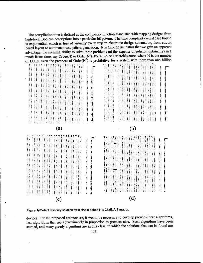
The compilation time is defined as the complexity function associated with mapping designs from high-level Boolean descriptions into a particular bit pattern. The time complexity worst case bound is exponential, which is true of virtually every step in electronic design automation, from circuit board layout to automated test pattern generation. It is through heuristics that we gain an apparent advantage, the seeming ability to solve these problems (at the expense of solution optimality) in a much faster time, say Order(N) to Order(N2). For a molecular architecture, where N is the number of LUTs, even the prospect of Order(N ) is prohibitive for a system with more than one billion
a * * %. * » * « ^-s rar r* ******* ■*■*»*
i i t *■»««< * * t *<«<*!* * >
* * ' I l * ' I I ', ' i i i - ! * * j i i ! t- i i i < i ! i i i ; ; i ; ; i < i <;'■'•! J ; j J \ \ ; I „ , i
■• ' ' * ' ' ' I I \ ' I \ I - I - I ■
■J S ! "■ ', i 'i ! 3 > J j I | i i • i ■i i < i ( ! ( ■ « i , ( ! * ^ ., i i « . i ) i J i t ( i ; -■ < ■
H ! : i ! : i * i i I ! U : : i :
^ * i * * 1 * s ■■! S » * * * * * «= * .J J J «- * .* i * ■* * t * ( * I* *- ! fi i ( » i i I t :i i » i J ( * t " ?
* i i » if i * f *■ S ;
j t if s * j s i ■? s r
.( ? s j j i * * * *■ t
* * # ^ * j * * > t
t ?■ \ -i s
* s- * ■i *
(a) (b) H :l* * * $ * * * &
t i
*r * <# *i » * 4* !■ 3 j w * ■* 5- # i- * ** !« a »*■■ * m ■<? * » *■ 3.;
j j J M j : | | ; J ; | j i; j ; \ \ \ I *'.((* jij; J ^ J J * * j * i % \ * i J J *
1- '\ f I ■■■■$, i ^ \ t % i ' * *j J *-*-** »
* t ? * '*i i K i * * * * 1 ^ * * "< t ' 4 .. J I * :» > »(*»«( t ■% t ! ^ I ' *
} * | *ip ; : j j I \ : i \ z i j ; ; * i 1 \ i ill j J ? * ? * * i t i * * t -j * ^
t * t *■ .'1 \ * i S 3 * * ;* * "■ ?■*■*** »..{(* :"3" | :. j f ■'?**■* ■» S * * J * *
s i | K '!!*: f * \ \ % t f f \ i i i t > -f
(c) (d)
Figure 14Defect discoerVisolation for a single defect in a 21xCLUT matrix.
devices. For the proposed architecture, it would be necessary to develop pseudo-linear algorithms, i.e., algorithms that run approximately in proportion to problem size. Such algorithms have been studied, and many greedy algorithms are in this class, in which the solutions that can be found are
113

often good enough but not the best possible answers. The programming time required for the proposed architecture will scale in proportion to the
number of tiles. Since the tiles are crossbar-programmed, access is random and the prograrnming time for a single tile is limited only by the speed of row and column address generation. Since the bitstream, once created, can be manipulated, it is possible to establish a large word width, in which each tile can be programmed in parallel. Since there are far more tiles than primary I/O, it is necessary to establish a compromise, namely that of dedicating a number of configuration streams to program sequences of LUTs in parallel. Under such an approach, as an example, it would be possible to program 2 billion lookup tables in less than 5 seconds, without any assumptions on transmission overhead.
Heuristics / Benchmarks In order to use a molecular architecture in practice, it is necessary to map Boolean designs
created with high level design tools into molecular descriptions. The tools to do this can be patterned after those used to perform partitioning, technology mapping, and routing in normal FPGAs. Our architecture poses special challenges. Whereas normal FPGAs have dedicated routing and logic resources, the proposed architecture permits any LUT to be defined as either routing or logic. This complication makes it difficult to harness existing algorithms. We demonstrated in Phase I that a fairly simple neural network model was capable of solving for design mappings, and as such we have one tool, though not a very efficient one. For the Phase 2 effort, we will develop a suite of tools that are capable of efficient solutions of designs specified at a system level, which will furthermore take tolerable defects into account. To improve efficiency, we propose to develop new and important extensions, based on sub-linear (design only for portions of the molecules used) and quasi-linear (algorithms that run roughly on the order of the number of elements) techniques. We furthermore will for the first time establish a linkage of the molecular FPGA to a commercial computer-aided design (CAD) tool, the Synplicity Synplify tool, which represents a 45% market share in the FPGA design market. To effect this linkage, we are partnering with one of the original designers of the Synplify system (Bill Cox from FPGA Technology).
We will develop a comparative benchmark program, in which a benchmark suite is developed for a 16,000 element representative device. The suite will be used to compare the performance of our architecture against a commercial architecture to assess the efficiency of the architecture. We will establish a strategy for demonstrating a scalable benchmark and will then leverage the Synplify tools and our custom extensions to answer the most significant mapping performance question: Is our architecture scalable logically as well as physically?
Performance Estimation Performance modeling will involve establish a parametric framework for estimating the
maximum frequency of operation for the molecular integrated circuit based on our architecture, its duty factors, and power consumption. The model follows directly from the architecture itself. In order to estimate the performance of the proposed molecular architecture, we must establish
the propagation delay through the LUT, the tile size, and the number of tiles between input and output. With the most difficult computation being associated with molecular structures themselves, it will be possible to quickly estimate the frequency performance and power consumption of an entire molecular integrated circuit based on reasonable maximum frequency,
114

duty factor, and usage conditions. As it turns out, traditional silicon FPGA devices work from similar parametric models which are used to guide application development.
^olAahHity Plan.
We believe it may be necessary to eventually harness at least the interconnection system of a VLSI system to perform the distribution of input and output (I/O) signals to enough points to permit effective utilization of molecular elements At the densities proposed, it will be possible to aggregate approximately 2,000,000 tile complexes/cm2, which is based on a 250 x 80 arrangement of the Figure 5 tile (3:1 depth, using the same width target as the demonstration system). The gate equivalence is design dependent, but a preliminary estimate suggests about 1000 gates / tile, yielding a 2 billion gate system. For interconnection growth estimates based on a low Rent's rule exponent (ft5), it is not unreasonable to expect that 10,000 I/O may be required, which translates to an x-y grid of a pin every 100 microns in each dimension. It is unlikely that an interconnection system can be deposited over the molecular circuitry. By such reasoning, it is necessary to consider the supply of I/O from beneath the molecular circuitry.
A schematic of the process involved with this inverted molecular-to-real world interconnection manifold is shown in Figure 13. It is based on the notion of harness both sides of a thinned silicon wafer (less than one micron) to exploit interconnections on two sides, one for the attachment of molecular circuits, the other for the attachment of I/O terminals. Since the process involves aggressive thinning strategies, it is heroic, but feasible based on epitaxial liftoff approaches and the existence of dielectrically isolated silicon and fully depleted CMOS semiconductor processes.
Sfalahility During this project, we propose to integrate work on computational system architecture, witn^
planning how to scale up from fabricating the 16,000 device demonstration chip level to the 10 device chip level. These topics are intimately related since issues such as testing and reconfiguring around circuit element defects could otherwise come to dominate the fabrication time as system size grows.
Our approach will include devising and categorizing design approaches that ease scalability at the beginning of the development cycle, evaluating trade-offs and necessary technology development, and working to incorporate them into the demonstration chip architecture.
We have defined what we believe and intrinsically scalable architecture, and we will seek additional enhancement to scalability into the system architecture. Before the two-year mark, we will produce a long-term scalability plan which describes the road map for scalmg this technology to the 1011 device level and beyond.
REFERENCES
[1] J. Reif., Private communication, June 2000.
[2] A.KDas, M. Pandey, A. Gupta, and P.P. Chaudhuri, "Built-in self-test Structures Around Cellular Automata and Counters", 'iEE Proceedings, Part E, 137(4):269-276,1990.
[3] S Chattopadhyay, D.R. Chowdhury, S.Bhattacharjee, and P.P. Chaudhuri, "Cellular-Automata-Array-Based Diagnosis of Board Level Faults", IEEE Transactions on Computers, 47(8): 817-828, August 1998.
115

FINAL PROGRESS REPORT INPUTS ON MOLECULAR ELECTRONICS ARCHITECTURES James Lyke, November 2000
Background.
The architecture work has advanced on several fronts, always reinforcing a central goal of establishing an architecture that could really work with molecules. The three basic constraints on architectures remain the same as they were stated before: (1) low interconnect demand, (2) amenable to self-assembly, and (3) defect tolerant. Our proposed approach, called Reconfigurable Cellular Array (RCA), is based on a cellular-automata (CA) inspired approach in which each site in a regular array is reconfigurable. The RCA provides a conceptually simple approach in dealing with these constraints, as suggested in the following table:
Constraint / Property Reconfigurable Periodic Arrangement Low Interconnect Demand X Lithography Alternative X Defect tolerance X
For convenience, the RCA architecture is summarized by way of the example shown in Figure 1. Figure 1 depicts a two- dimensional periodic structure (a tile) with nearest-neighbor linkages, which embodies a description of a simple CA. The circles represent configurable functions; these sites are usually referred to as «-input look up tables (nLUTs). For molecular architectures, the «LUTs represent nano-blocks, based on molecularly synthesized circuits that perform the required functions. The linkages of these nano-blocks are themselves expected to occur as a secondary level of self-assembly, in which the nanoblocks are brought together in a unified ordering which embodies the Figure 1 tile.
Figure 1. A portion of molecular electronics architecture based on a tile of 3-input look-up tables.
For reasons beyond the scope of the present discussion, the linkages
are directed. In particular, they form a feed-forward network. It is important to understand mat the both the linkage patterns and the HLUT definitions can be varied to either embellish the expressive capacity or simplify the implementation of the RCA. The need for simplification is important, since even elemental logic gates based on molecules are exceedingly complicated to construct. By reducing, for example, a 3LUT to a 2LUT (Figure 2), we can reduce the number of circuit elements by 50%. Reducing the linkages can also simplify the problems of the higher level self-assembly.
Figure 2. A portion of a simplified architecture based on 2LUTs. In addition to the constraints based on physical limitations, one
must address a number of constraints based on practical considerations, which drive the utility of an architecture. These are the "logical constraints" of architecture. We believe summarize some of these and how the proposed architecture addresses those constraints.
116

High Interconnect Demand. In direct opposition to the physical limits, architectures become progressively interconnection intensive as the scale (number of devices) grows. RCAs address the "hunger for interconnect" by allowing any site to be configured to behave as either logic or interconnect. The manifestation of interconnect intensiveness in design can be explained in some respects as a degradation of efficiency, since cells that could otherwise be defined as logic must be sacrificed as virtual wire. Similarly, "real world" reconfigurable logic devices, also known as field programmable gate arrays (FPGAs), also suffer from efficiency problems [dehon95].
Turing machine equivalence. This constraint refers to the logical capacity of expression in an architecture. It is said in the field of computer science that an algorithm is computable if it can be described in a way that can be programmed to run on a Turing machine, [dewdney] Turing machines, being the "reference model" for analytic work on computational complexity theory, can be directly related to real-world computers, such as a Pentium. With full control of logic, memory, and interconnect structures, which are used to construct real-world computers, it is possible to construct "Turing-complete" architectures. With any one of the three missing, it is simply not possible to form a Turing complete architecture. The RCA-based architectures require feedback to meet this constraint rriinimally, and we have described mechanisms for incorporating feedback in RCA tiles in previous reports on this effort.
The next two constraints are derivative, due to the use of imperfect and reconfigurable "media" for the implementation of "target" architectures. It is sometimes a confusing point that reconfigurable architectures are "source" architectures, while they designs that are programmed into them are "target" architectures.
Ease of defect identification. Almost all computation structures are non-random, yet lack a simple descriptive pattern structure. Sometimes the property of descriptive complexity is referred to as Kolmogorov complexity [kolmogorov]. Qualitatively, it is easier to verify structures with simpler descriptive complexity (such as RCA tiles) than for elaborate structures in which latent defects can be easily obscured and difficult to isolate. In RCAs, defects represent easily-identified departures from patterns that are simple, observable, and lend themselves readily to exploration through the inherent reconfigurability of the approach.
Ease of supporting reconfiguration. The ability of an architecture to be configured is simple as a superficial consideration. In each case, a memory array is involved. The two most common approaches for setting values in a memory array involve crossbars or shift registers. In each case, attention to defects and overhead in implementation (e.g. address decoding) must be considered. Our work has identified the possibility of harnessing both concepts and new approaches are identified for reducing implementation overhead.
Even with an approach meeting these constraints, it is important to be able to define the final product implied as it might be compared to an ordinary silicon-based integrated circuit (IC). With a very-well established infrastructure, very clear and focussed concepts have emerged for mounting, operating, and interfacing silicon ICs. Many of the Moletronics efforts, including our own, have suffered from lack of a credible bridge to span from nano-scale interconnections to macro-scale electrical terminals. In other words, no viable packaging concepts have been identified that would allow molecular electronics to fit into an established framework that is expected in ICs that have been developed over the last three decades.
117

Simplifications of the Basic Architecture
We have described a simplification of the original 3LUT-based architecture to an architecture shown in Figure 2, which removes exactly one link from each node to produce a new type of periodic grid based on 2LUT nodes. Since LUT complexity scales as 2* (N being the number of inputs), using the Figure 2 grid results in node designs that are at least 50% simpler.
But we sought further reductions in complexity, and we have identified a more produce-able 2LUT node design. Why? Even the 2LUT structure could be too diffficult to tackle as a single synthesizable molecular circuit. For this reason, we have identified a much simpler structure, which appears to be similarly capable of universal Boolean representations, though not in exactly the same way as a "canonical" 2LUT structure. The basic new structure is a degenerate LUT, involving a single input and output. The 1LUT (Figure 3), capable of expressing only four Boolean functions (summarized in Figure 4), appears to be of little use and has never received any attention in literature. By adding a molecular resistor to the 1LUT (Figure 3b), we can form the structure shown in Figure 3c through a self-assembly process in which the "resistor end" is attached at the same point by two different structures. Under the scheme of an RTL (resistor- transistor logic) system, we produce a structure equivalent to the one shown in Figure 3d. Under a periodic arrangement of these structures, dictated by the Figure 2 guiding template, a simplified tile, reflected in Figure 5 can be formed by replacing all 2LUTs in the Figure 1 grid with Figure 2c structures.
© ß
(c) (d) Figure 3. An approach to simplifying 2LUTs. (a) 1 LUT as a sub-nano building block, (b) Addition of a molecular resistor to complete the sub-nano block, (c) Depiction of physical self-assembly of 2- 1LUT blocks, (d) Resulting logical equivalence. This tile and lLUT-based compute structure is flexible
enough to implement general digital functions. A simple example based on a one-bit half-adder is shown in Figure 6. This diagram illustrates the evolution of routing and logic computation as signals feed forward within the tile to form the desired functions.
Tiles are the basis of a molecular compute structure, but each node must be configured. The 1LUT structures require two bits of binary storage, and the storage can be configured by either a shift register or a crossbar. Our more recent work has focused on the crossbar, resulting in a memory "field" as shown in Figure 7. The field is a x-y distribution of individual memory cells, and four cells are required in each of the Figure 3c structures. A unit cell based on two cross-strapped Figure 3c structures is referred to as a "bowtie", which requires eight bits from the memory field to be configured.
118

in Uffaaaqg out 0 ui
1 ^2
in out in out 0 0 0 1
1 0 1 0
in out in out 0 0 0 1
1 1 1 1
One approach to molecularly synthesizing a tile based on the lLUTs on an x-grid is to first form the memory field, and then assemble a pattern of "bow-tie" nano- modules on top of the memory field layer. The "unit cell bowtie" must span eight memory bits from the memory field, and Figure 8 illustrates two possible ways this self-assembly might play out in an actual molecular self-assembly process.
Defect Discovery, Isolation, and Mitigation
We can heuristically argue that defects can be readily exposed in structures with low descriptive complexity, since those departures from ideality actually result in an increase in the information entropy of the resulting
Figure 4. The one -input look-up table (1LUT) and its four functions. structure. One can easily prove this entropy increase qualitatively by conducting a simple experiment. In this experiment, one creates two simple, identical text files with a text editor, each containing exactly 256 "l's", and no spaces, tabs, line feeds, or carriage returns. In the second file, one of the "l's" is randomly replaced with a "0". Next, the files are compressed with, for example, a ZIP compression utility. When the resulting file sizes are compared, it is clear that the second file requires more space. Defects in a simple structure, therefore, increase its complexity.
Figure 5. A new tile based on lLUT/resisor sub-nano blocks.
1 2 4 b
5 6
a a b b -
ab ab ab - -
- a? b ab
Figure 6. . How a single -bit half-adder could be mapped onto a lLUT-based architecture.
We believe the simple properties of periodic architectures lend themselves to very simple defect discovery approaches. To demonstrate this point, we again resort to a simple experiment. In defect discovery, it is first very important to have the knowledge of structure. In the cases of random architectures, which some groups have proposed in the Moletronics program, it is necessary to undergo another phase, which we refer to as "structure discovery". For defects are quantified as departures from ideality, and in order to know what is ideal, we must know our starting point. For this experiment, we choose a 21 x 46 array of 2LUTs, shown in a spreadsheet simulation in Figure 9. Next, we introduce a defect, and its impact is clearly detectable upon
119

inspection of Figure 10. Specifically, in this simulation the 2LUT at row 5, column 5 is defective. It is important to note that this spreadsheet demonstrates a level of observability that is not possible to achieve in real life, and in fact our observations in a real case are limited to the sites on the bottom row only, since that is the interface point for the outputs of the tiled structure. So while the simulation will make the location of the defect seem obvious, it is in practice not possible to deduce the defects so readily.
hifcifcfcibifc.kifc.fcikiii .b.k.fc.fc..k.b.fc.,L,b.fc,,L, LLI11114I41 jkih.bijbihibihifcibihifci
-•'-'•'i »,fc,,fc,
jkikiftikikiBihif
Figure 7. A molecular memory array based on a crossbar approach.
So, while we know where the defect is really, we must confine our deductions to observations of tiie patterns on the bottom row only. Our first step in the "geolocation" process involves configuring all of the 2LUTs in the entire tile to behave as
"straight wires". The determination of this configuration obviously involves little intelligence or planning in terms of computation as in fact all sites are configured me same way .The result of this test is shown in Figure 10. The bottom row in Figure 10 reveals a missing "1", and we know that this means any one of the 2LUTs in column 5 could have been responsible for this defect. So, we could say our "ambiguity group" is of size 46. A second test involves using a second "global program" for each site, in this case an XOR pattern, producing the Figure 11 pattern. Once again, no special efforts have been made to form a more complex triangulation. Rather, we have done a fairly mechanical thing, in that no unique site programs or input signature patterns have been computed. Yet, as we see in Figure 12, based on but two "un-premeditated" patterns, it is possible to collapse an ambiguity group from 966 sites to 46 sites to 2
fcibibifctfcikifc h fc bifc. t.fcit.h.fc.fcibfcfcfc.t fcifc.fcikikifc.bhfcfc'fc fcifcifc.k.k.k.kb.kkifc - Lll
fciii»,
fc-i»i5!.>M<ibäci|ifc'
Figure 8. Attachment approaches for dual 1LUT blocks that would be self-assembled onto the molecular memory tiles. sites. We do not here carry out the final act of configuring the LUTs in a third test, in which it is easily possible to conceive a nearly infinite number of ways to, in a single configuration step, produce a final test to isolate the fault to one unambiguous location.
120

Steps toward programming heuristics in perfect and defect-ridden molecular tile structures
1.1 \ „mvCn?pr,A ^ hieh-level Boolean designs are translated to a large number
bitstream, tne aignai ^f- rnmn]fJd;dtal svstem The same s natation wül occur "with high
resources, our architecture employs homogeneous *™«? *?■"? FPGA fciklogb « decomposed
to this effort, we have made beginning steps towards establishing heuristics for ^onBgurable cellular
LT™ ba this case, we must allow for the ^°f°X £tSU *e standard defects which represent alterations in the graph. In practice, tor otner *™* ™^™~V. Sfalmfct this type of flexibility, but as a rule, such features are not incorporated in
contemporary FPGAs.
Whether for logic, routing, or both, it is important to once ] | j again point out that the heuristics are classified as having a ; ; ; worst-case computational intensiveness that can approach |:, j exponential time. The situation is referred to as NP- J[- complete (ISfPC), meaning that it is not possible to bound ..,, . the time required in the worst case by any finite ||! polynomial. As such, a higher-order polynomial more and ; j ; more resembles the Taylor expansion of the exponential u-\ function. Fortunately, most real-world instances seem to |{- ; be solvable in much shorter time. In fact, any heuristic that ;,; has a time complexity function much worse than N 2 ^ would take an intolerable amount of time. When a ;;; computer-aided design (CAD) problem takes longer than y : that it is usually the case lhat the designer intervenes, ; v
stops the compilation, and re-runs the ahjorithms after simulated 2LUT tile. making some minor adjustments to the design or fee *»g«™ solution boundary conditions. It is ^ef°^^m
usands ofNPC problems, we often find that many order to function in the ^i^^a^^yW^Sede that we are rarely going to
intractable on the scale of human existence.
121

« ? t i t t t * ! * ( < *i ( T ) » i T > ( "I i ! 1 r .* • ■-. i t ■ t * i v i J ) : v *
( i ( • J t i * 1 ( ! ■ \ i
Figure 10. Simulated 2LUT tile with defect and test program. Each 2LUT is programmed to behave as a straight wire. The bottom row shows the defect as a single missing "1", which could have been caused by any defective LUT in the column.
We see no fundamental differences in the situation with molecular architectures, except for an intimidating scale factor. The template of finding an algorithm for NPC problems involves two basic principles or steps. The first principle of a heuristic is to establish a greedy algorithm. Many greedy algorithms operate at near linear term, attempting to obtain a quick answer based on some principle such as minimum weight or shortest path, etc. The greedy algorithms are considered to be dumb, because they lack the sophistication to "look under rocks" or explore subtle nuances in the search space that lead to significant improvements in the answers theyvfind. But, for whatever their shortcomings, greedy algorithms are fast and do find a starting point. It is possible that a good greedy algorithm can be considered the end product, and this may be the case for molecular architectures, since we do not imagine that even an N2
algorithm will be acceptable.
The second principle of heuristic involves some "smart" approach in a nuanced exploration of an exponential or
factorial search space. This is more often itself called the "heuristic" as it is based on a philosophy other than brute force. Heuristics for NPC problems are varied, but include back-tracking, depth-first search, simulated annealing, dynamic programming, genetic/probabalistic algorithms, and so on. In fact, almost anything qualifies as a heuristic so long as it is: (a) not itself a "greedy" solution, (b) capable of finding better answers than a "greedy" solution, and (c) capable of "good" average case performance.
So far, we have concentrated on the routing issues associated with the molecular tile, with the rationale that interconnect issues will dominated in the design process. One of the remarkable properties of the molecular tiles that we have studied is their ability to
s s ' * * T i » a ii i; i] « i» r* I" !* *9 7i ai l * . 1 1 i * 1 % I i -i 1 « i i * A ■< 1 1 ' t -?" * ■ 1 * 1 I s < » I t .« 1 * 1 ■! * » * f « \ t A t t t i * « ■ * 1 I * \ -f 1 1 i • * i
i * i i i i l t i l. * i i * 1 ? t i * i t i 1 A 1 < 1 I 1 i •. i t j i « i > » 1 '■ i ♦ »
i * i i * -i t * t * t .'i i i « * 1 * i * t f !1.1ü-1i<si?tt1'l ""'. 1 1 * 1 * 1
1 1 V 1 * 1 t * t I t 1 1 1 -* 1 1 * 1- .S .1 * -1 1 '« ■« < 1 I * t t 1 I < t ■* i 1 » i t 8 v 1 1 '. 1 • 1 t < t > 1 I V | "J I 1 t 1 1
* 1 i =■*' 1 * 1 j < t » * t t f' i ' i '■* » % 1 >. i i i i ! i i * i • % t s 1 t t < i ■* ■» s i t * t * 1 I i I ♦ < 1 < I ! t i < t 1 * < i > 1 t 1 < i * * 1 1 1 t 1 t * f * 1
*■<«*«! ä 1 *.<*** I * t < * « * 1 * i t 1 I t i ! * i T I t 1 ■* i i * i * i t t 1 ( ( ■ 1 I * I 1 I 1 1 ü '» 1 ■* 1 t 1 * 1 } -■* t i -J -t '. J 1 I ! I ■* 1 ? ' 1 .T 1 * i t ■ s < • » i i t 1 < v- «■ ^ "» -1 * r * * T •» i ■ i f j ■< i i T 1 f *■ ) -i 't i * ' ii *
>lf1^ *1 » * t * .1 < ^ * * * ■• * i ■« ■ i
*-i '-«i si ti-ts -II*I »iii's ■)
* < ■ i" i ? i i * t j ( 1 * t . 1: i I 1 ! t ■ l t * 1 1 1 < 1 1 1 1 :« 1 t < I - -t . 1 « 1 ■ * * .f ■* 1 1 1 J 1 1 1 t t i I 1 1 '1 « 1 *! 1 1 i A i i 1 f. i i * t ! t i f 1 '■ * i i * ■? "i * i i ■! ( * i » i i » * < i i * i i i * i
* 1 1 *. * '. i \ * 1 t 1 ( i 1 < t i i -t < T 1 t t t ! f 1 1 1 * t I t t ,t T 1 » ■* 1 » 1 I 1 1 » 1 t * 1 t 1 1 ^ « t I « I . 'S 1
* « i .. * 1.. s i i < i * i y 1 ' " t i 5 ' v 1
i i ( » 1 s i ! ■; t i i * t * i i i i i i
Figure 11. Simulated tile with second test program. Each 2LUT is programmed identically with the XOR function. be analyzed as pure mathematical structures. For example, if we are trying to create a greedy approach for routing we might use the following principles:
Figure 12. Simulated tile with second test program. Based on the bottom row pattern, only the two shown sites could have caused the defect.
122

PRINCIPLE #1: Separate unrelated signals as much as possible.
PRINCIPLE #2: Bunch I/O assignments for large functions more closely;
PRINCIPLE #3: Bunch I/O assignments for functions mat depend upon each other more often closer
together.
PRINCIPLE #4: Use the most important routing resources later in the solution process.
PRINCIPLES #1 - #3 are useful in establishing an initial preferred location for input signals. One important property of the tile structures is that due to the localized nature of the connective network, there exists a "cone of influence" for signals in a tile. In order to interact with signal, it is necessary to be within this cone. As such, if signal A never interacts with signal B, then their respective conesiof influence need never overlap (PRINCIPLE #1). Conversely, if a function F is an mvolved function of signals A,B,and C then it may make sense to bunch signals A,B,C closely together and have F in a column that is central to the cluster. Such placements make it more likely that a tile program solution will be found without back-tracking and altering the initial assignment.
In the case of PRINCIPLE #4, we must interpret what "important" means. A reasonable mterpretation S be the cardinality of paths in the light cone of a signal. To illustrate the meaning of this property, we form a simple spreadsheet in Figure 13. Each number is physically located in each a tile Position of a small 3LUT tile, and the numbers represent the number of paths between the cell itself relative to the central highlighted cell position. In this case, the LUT positions in the column below the highlighted cell have the highest value In fact, if we simply focus on the column and examine the integer sequence Ü13 7wTmm,l 107,3139,8953,25653,73789,212941,616227,1787607, 5196627,15134931 44152809 '128996853, etc.), we observe that these numbers correspond to the coefficients of ai central Saornial expansion: (l+x+x-2 )" [hoggatt]. (It turns out that 2LUT path cardinality corresponds to the coefficients of a central binomial expansion [integer]). . The significance of the these integer sequences is that they are readily computed, making their use in heuristics more convenient. If the cardinality of paths is a guiding principle then solution paths between I/O and intermediate solution are readily chosen by direct computation.
123

™*WH~~™~~^
1 |
LZZZ~° 0 1 1 1! OS Oj 0 0
0 1 2 3 2| it ÖI 0 0
i 3 6 7 6 3j 1 0 0
nzzzzii 10 16 19 16 101 4 1 0
15 30 45 51 45 30 15 5 1
50 90 126 141 126 90 50 21 6
161 266 357 393 357 266 161 77 28
r~~~5oT 784 1016 1107 1016 784 504 266 112
1554 2304 2907 3139 2907 2304 1554 882 414
4740 6765 8350 8953 8350 6765 4740 2850 1452
14355 19855 24068 25653 24068 19855 14355 9042 4917 !____
58278 69576 73789 69576 58278 43252 28314 16236 ,____
171106 201643 212941 201643 171106 129844 87802 52624
r 388752 502593 585690 616227 585690 502593 388752 270270 168168
* 1161615 1477035 1704510 1787607 1704510 1477035 1161615 827190 531531
3465840 4343160 4969152 5196627 4969152 4343160 3465840 2520336 T6654li1
T0329336 *T2778?52 14508939 15134931 14508939 12778152 10329336 7651632 5182008 ;___
37616427 42422022 44152809 42422022 37616427 30759120 23162976 16031952
"91538523 1.11E+08 1.24E+08 128996853 1.24E+08 1.11E+08 91538523 ̂ 69954048 49366674 ,___
3.27E+08 3.64E+08 377379369 3.64E+08 3.27E+08 f2.72E+08 J2.11E+08 1.51E+08
8.1E+08 9.63E+08 1.07E+09 1105350729 1.07E+09 9.63E+08 8.1E+08 [6.35E+08 4.63E+08
2.41 E+Ö9 2.841+09 3.14E+Ö9 3241135527 3.14E+09 2.84E+09 2.411+09 1.91E+Ö9 1.41E+09
7.15E+Ö9 8.38E+09 9.22E+09 9513228123 9.22E+09 8.38E+09 7.15E+09 5.73E+09 4.29E+09
2.13E+1Ö 2.48E+10 2.71E+10 27948336381 2.71E+10 2.48E+10 2.13E+10 1.72E+10 1.3E+10
6.32E+10J7.31E+1C 7.98E+10 82176836301 7.98E+10 7.31E+10 6.32E+10 5.15E+10 3.95E+10
So based on these principles, it is possible to make at least a semi-intelligent algorithm for routing,m periodic tiles We attempt to illustrate aspects of path cardinality-driven placement m Figure 14. The placement of signals a,b,c, and d reflect close-coupling by the overlap of their respective cones of influence while signal g is placed further away, since it is only a function of the output of some composite of a,b,c,and d, as evident in the solution shown in Figure 14b. Had signal g on the other hand been randomly placed within the grouping, the resulting implementation would have been less efficient, as reflected in the solution shown in Figure 14c. We consider Figure 14c less efficient than Figure 14b because it excludes more LUTs from being used in future parts of a more involved solution process.
124

(a) (b) (c) Fieure 14 Illustration of effect of I/O assignment on solution process. Left shows a pnncipled assignment of I/O of a complex function. Center shows a solution based on this assignment. Right shows a solution based on a more random I/O assignment. The effect of toe two approaches is that random assignments result in lower efficiency (more LUTs consumed in Ihe solution process).
REFERENCES
[dehon95] DeHon, Andre. "Reconfiguable Architectures for General-Purpose Computing," AI Technical Report 1586, MIT Artificial Intelligence Laboratory, 545 Technology Sq., Cambridge, MA, October
1996.
[brayton90] @ARTICLE{BRAYTON90, author = "R.K. Brayton, G D. Hachtel and A.L. Sangiovanni- Vincentelli", title = "Multilevel Logic Synthesis", journal = "Proceedings of the IEEE», year ="1990 , volume = "78", number = "2", pages = "254-300", month = "February", note = "*" }
[dewdney]@BOOK{dewdney, author = "A.K. Dewdney", title = "The Turing Omnibus", publisher = "Computer Science Press", year = "1989", address = "Rockville, MD" }
[hoggat] V. E. Hoggatt, Jr., and M. Bicknell, Diagonal sums of generalized Pascal triangles, Fib. Quart., 7 (1969) 341-358 393 This reference was discovered by examining the On-Line Encyclopedia of Integer Sequences ( http://www.research.att.com/~njas/sequences/), and this is sequence number A002426.
[integer] On-Line Encyclopedia of Integer Sequences (http://www.research.att.com/~njas/sequencesO,
sequence number A001405.
[kolmogorov]@BOOK{kolmogorov, Ming Li and Paul Vitanyi, An Introduction to Kolmogorov Complexity and Its Applications, second edition, Springer-Verlag, New York, 1997.
125

submitted to the AIAA Journal of Spacecraft and Rockets, December 2000
Cellular Automata Based Reconfigurable Systems as a Transitional Approach to Gigascale Electronic Architectures
J.C. Lyke, G.W. Donohoe, S.P. Kama Air Force Research Laboratory, 3550 Aberdeen Ave. SE, Kirtland AFB, NM 87117-5776
Abstract Research in molecular electronics has but one motivation:
to carry Moore's law scaling in electronics to the year 2050 or beyond. The result will be staggering, continuing to transform our lives as has the current evolution of micro-electronics since their inception in the 1960s. Designers of molecular computers will also undergo transformations in the way they design digital processing architectures, due to new constraints in what may be the most aggressive fabrication technologies ever conceived. It becomes necessary to increase focus on the pursuit of basic feasibility of a giga-scale architecture so that tenant design, test, and implementation issues can be forecast and researched. Our work has led to the development of an architectural media for molecular computation. A cellular automata-inspired template forms the basis of a one billion gate (giga-scale) testbed, which involves the use of 3-D, paper-thin, ultra high-density multi-chip modules to assemble a reconfigurable design that is scalable an additional billion- fold, consistent with the density projections of three- dimensional circuits based on molecular electronic devices. The periodic nature of the architecture not only addresses significant constraints in molecular-scale systems design, but can make this demonstration tractable, as the reconfigurability can be exploited for self-test and defect tolerance.
I. INTRODUCTION
Moore's law asserts that the number of transistors in a fixed area doubles about every 18 months, a trend now codified into industry's roadmaps and an indelible expectation of a technology-affluent society. The future is not without its problems however. As the feature sizes of the integrated circuit (IC) approach 0.1 micron, over ten kilometers of wiring will be required for each square centimeter of circuitry [1]. This underscores the central influence of interconnections on architecture. Researchers have highlighted that future giga-scale (> 109 gate) architectures will suffer from potential reductions in speed due to an increase in average interconnection length [2]. Even if the intent of Moore's law can be achieved through progressive reductions in transistor size, further progress in high-performance architectures may be stymied by the inability to wire complex designs.
Despite the monumental real-world architecture-driven problems of interconnect, some researchers are working towards a far more aggressive vision of molecular scale electronics, in which individual active devices are based on a single molecule [3]. Assuming that such molecular implementations are restricted to two planar dimensions, the resulting theoretic densities are potentially one million-fold
over today's CMOS-based microelectronics. Of course, molecular implementations need not be limited to two dimensions, and these approaches may be the first to realize an additional million-fold density advantage by exploiting the third spatial dimension. Neglecting to do more than mention the tremendous challenges in molecular synthesis and assembly themselves, three other challenges are obvious to what may be the densest possible approaches in future electronics: (1) interconnection supply, (2) lithographic alternatives, and (3) defect mitigation.
A prospective architecture, inspired by simple cellular automata (CA), may offer an elegant solution to these problems, since CA embody the concepts of periodicity and localization of interconnect, both of which hold promise for molecular approaches. By allowing the computation at each site in space to be arbitrarily defined from a simple but complete space of Boolean functions, a simple and potentially effective cellular field programmable gate array (FPGA) is formed.
As a precursor to future molecular computer architectures, this paper describes novel digital reconfigurable components, ultra-dense packaging, and how silicon-based versions of these components can be aggregated with packaging. This is the basis of a cellular FPGA, which is dense, scalable, easily tested, easily programmed, and defect tolerant. A near-term proposed demonstration would have a theoretic performance ceiling of 1017 operations/second, while achieving a packaging density improvement of 100-fold over today's best alternative packaging approaches (50 cm silicon per cm3).
n. AN EMPIRICAL VIEW OF ARCHITECTURE
Architectures, particularly those implemented in hardware, have properties that are today only empirically understood. Rent's rule [4], for example, is an attempt to model the relationship between the internal complexity of an architecture and the number of terminals required for external communication:
T = A-GP, where T is the number of terminals, G is the number of
logic gates, A is the average number of pins per gate, and 0<p<l is Rent's exponent. In complex architectures, Rent's exponent takes the value, 0.5<p <0.8 [5,6]. Renfs exponent is low for systems with regular structure, such as memories, and is highest for complex Application Specific Integrated Circuits (ASICs) [2]. Random circuitry has no Rent's rule (i.e.,/>=!), which suggests that something is naturally imposed
126

submitted to the AIM Journal of Spacecraft and Rockets, December 2000
by humans in the act of design that provides for the structure that Renfs rule attempts to capture. Though the mathematical concept of separators/bifurcators offers some insight [7], Renfs rule is still not completely understood. What is possible to say, however, is that Rent's rule does seem to capture aspects of hierarchy [5], dimensionality [8], and likely the descriptive complexity of Boolean functions implemented in architectures [9].
For very large gate counts (MO9), referred to as "giga- scale", Biafore [2] has shown that the average interconnection length increases when the Rent's exponent p> 0.5, resulting in increased propagation delay. Since most complex architectures have high Rent's exponents, present concepts such as Pentiums with OßO1) gate counts may face severe performance bottle-necks as they pace Moore's law curve m the future.
A logical alternative to contemporary architectures in the transition to ultra-high gate counts involves the exploitation of simple and highly parallel cellular automata concepts to form a scale-able computation fabric [10]. Cellular automata (CA) come in many forms, but the most commonly discussed implementations are the binary versions popularized by Wolfram (1-D) [11] and Conway (2-D game of life) [12]. CA can be thought of as a finite mesh in m-dimensions of discrete points Each point in the lattice performs a simple computation, based on the values of sites in a usually small, symmetric, uniform neighborhood. The values of all sites are usually computed simultaneously at discrete points in time. CA structures based on spatial dimensions with small neighborhoods have low Rent's exponent (p< 0.5) and avoid the interconnection bottlenecking problem associated with
scaling.
in. MOLECULAR FPGA CONCEPT
We use the CA concepts to build novel FPGAs. Most previous CA based architectures for computation have used identical functions or rules to compute the values of each site based on the values of neighboring sites [13]. Here, instead of using fixed and identical functions at each lattice site, we permit distinct logic functions at each site, in the form of look- up tables (LUTs), which establish a complete Boolean basis function set. We introduce a planar tiling of look-up tables (LUTs), formed by unraveling the space-time behavior a three-neighborhood 1-D CA into a two-dimensional spatial feedforward network, shows one of the simplest periodic implementation of a reconfigurable CA based architecture involving LUTs. It is clear from the figure that the Boolean functions at each site, which will contain one or more molecular device unit(s) (MDU), can be distinct, arbitrarily selected from a complete Boolean basis set. This, in contrast to the single-function-per-site CA architectures [11], allows for considerably improved flexibility, especially since different sites of MDU can be specialized for different functions. Furthermore, this particular CA "tile" uses a directional neighborhood, in particular a feed-forward network. This restriction is non-essential, but enforcing it results in more tractable implementations, as the possibility of forming localized feedback hazards is eliminated.
As in the case of other reconfigurable FPGAs, user designs in the present architecture are defined through the mapping of arbitrary logic descriptions in terms of LUT functions [14,15]. The ensemble of LUT "codes" can then be
Outputs
Figure 1. Acellular field pfogr—.e gate array ^^ cellular automata (CA). The upper left diagram of a to^'f^^-^^^S^Si teft diagram establishes an equivalent on the site and its nearest neighbors. The CA evolves * dlsOTte^™ ^^^^ If each .epresenta^non in which each^w^^^ site is replaced by a binary look-up table p , wracn i*ui «P « jmni-mentine more complex Boolean networks than the original
127

submitted to the AIM Journal of Spacecraft and Rockets, December 2000
Figure 2. Illustration of how molecular LUTs can be programmed with a serial configuration chain. The signal interconnections used in operation of the FPGA propagate vertically downward in a feed-forward network, while the configuration system used for programming propagates horizontally (meandering) and upwards.
concatenated to form a serial digital bitstream. If the LUTs are implemented as memory cells in a shift register, it is possible to program an entire design by shifting its corresponding bit pattern through the tile of LUTs. This is shown in Figure 2.
In order to form a complete CA architecture, it is necessary to introduce user storage and feedback to allow the definition of generalized state machines. To do this, linear register arrays are introduced at one or more tile edges, and multiple tiles are juxtaposed. An example tile arrangement is shown in Figure 3. Each tile then propagates a combinational circuit block realized within the LUTs of particular tiles. The registers, when synchronized to one or more global clock signals, define the operation cycle of the overall FPGA. In order to achieve true feedback, the tiles must permit 360 degree signal propagation loops. A possible arrangement in our proposed cellular FPGA for achieving true feedback is shown in Figure 3 through four tiles, each rotated 90 degrees.
It is both interesting and useful to compare cellular FPGAs to traditional FPGAs developed by industry. They are similar in that both types of FPGAs use LUTs and are configured with a serial bitstream. However, cellular FPGAs differ from traditional FPGAs in two important aspects. First, cellular FPGAs do not support programmable routing. In commercial FPGAs, as much as 90% of the silicon real estate (space on the substrate of an IC) is represented by interconnect [15]. Cellular FPGAs, which only support nearest-neighbor connections, must define interconnections through the use of LUTs. Of course, this also requires that LUTs must often be sacrificed as virtual wires (the case where a LUTs behavior is defined to simply repeat one of its inputs) for the purposes of signal transportation. The second important difference is that cellular FPGAs are by definition periodic, whereas commercial FPGA devices have complex, irregular structures.
A third, and perhaps one of the most important characteristics of cellular FPGAs is its defect tolerance. In order to illustrate this a bad LUT and its impact zone ("cone of influence") are shown in Figure 4(a) The effect of the bad LUT can be easily recovered by simply adjusting the definition of neighboring LUTs to circumlocute or "steer" around the defect (Figure 4(b)). This very important property of cellular FPGAs builds upon the periodic nature of the design to produce, in principle, very robust complex architectures, capable of dealing with many distinct fabrication or assembly defects.
£ | _> X E
*§
VDarrayof ,, ntlip^lops CLK
H
1-D array of n flip-flops
mxn LUT array
Figure 3. Formation of more complex device by hierachical assemblage of Figure 1 tiles into a feedforward network. Each of the four tiles in this architecture are directed at 90 degree rotation to form an overall feedback network. Linear flip-flop arrays form registration structures, which are necessary for the construction of finite state machines. Clock distribution is required only for these linear arrays, as depicted by the central structure.
Figure 4. Demonstration of defect tolerance in cellular FPGA. These diagrams represent implementations of Boolean networks in a cellular FPGA tile. Solid circles (LUTs) with connections implement non-trivial functions, circles with a vertical line implement virtual wires, and unconnected circles are electrically inert. The left diagram illustrates the impact of single defect (D, row 2), which has a "cone of influence" represented by the dotted lines. In this case, two of four output functions have been corrupted by the defect. By redefining LUT configurations within the same tile, the right network circumlocutes the defect, resulting in a successful implementation of the desired network, even with an imperfect tile. Such reconfiguration schemes will be essential in any molecular electronics approach.
IV. GIGASCALE DEMONSTRATIONS IN SILICON
Although the present cellular FPGA concept is intended for molecular scale implementation, it can be equally easily
128

submitted to the AIM Journal of Spacecraft and Rockets, December 2000 submitted totne A y ^ ^ ^ ^ fe ^ ^ ^ ^ ft 3_D ^^
as shown in Figure 7. In this approach, individual layers can be incrementally stacked together, using a single additional patterned overlay. This will allow contacts between nearest
neighbor layers to be ^^"«^J«**
adapted in many other technologies, including traditional very large scale integrated (VLSI) circuits. The ability to assemble near-term prototypes in silicon provides an excellent opportunity to study giga-scale architectures firsthand. In 0 25 micron CMOS, for example, it is possible to assemble 200,000 3-input LUTs (3-LUTs)/cm2. As such, assuming an effective gate equivalence of five, two-input gates per 3-LU1, the cellular FPGAs offer a gate density of 10 gates/cm .
While the density of a cellular FPGA is impressive and competitive with traditional FPGAs, in order to implement a giga-scale demonstration, it will still be necessary to accumulate over 1,000 cm2 of silicon in a small^region^ For this reason, it will be necessary to consider not only multi- chip modules (MCMs), which might offer an increased planar density, but three-dimensional techniques are «quired to achieve a giga-scale architecture in' a manageable physical size. For this purpose, we introduce the notion of an ultra- high density interconnect (UHDI), capable of implementing a dense 3-D arrangement of cellular FPGA components.
The basic high density interconnect (HDI) process is widely reported as a refined implementation of a patterned overlay interconnection process for building dense MCMs ri61. By employing a temporary substrate and using back- ing techniques, a paper-thin MCM technology' which we call UHDI can be defined. The process of generating UHDI is illustrated in Figure 5. The finished UHDI assembly (Figure 5(c)) is similar to HDI, except that the entire module, including substrate and IC components, ™J?^ *™£ It is very important in the 3-D extension of the UHDI process that (1) a minimal number of patterned overlay wiring layers be used and (2) the module be thinned in its entirety to less than 100 microns. The plies may be individually tested and
(a) substrate with recessed components (face up)
(b) formation of single layer patterned overlay
(c) thinning of entire module through back-grinding
Figure 5. Simplified sequence of ultra-high density interconnect JSS) fabrication process, a. A substrate hosts integrated ctfcuite (ICs) face up in recesses to produce a planar surface, b. A kapton dielectric (25 u) is then laminated onto the substrate. Vias are MMKI- kapton, and a Ti-Cu-Ti (1000 Angstroms /4u nZ Angstroms) metal system is deposited,patterned^jdjjW, creating a first-level interconnection manifold, c. The substrate ana embedded ICs are uniformly thinned to produce a 70-100^ paper- rnui multi-chip module (MCM) ply, shown in F.gure 6, which can be electrically tested.
even used as a decal-like MCM for a variety of applications- Simple MCMs have been built using this technique (Figure 6) resulting in a 100 micron structure. The final thickness of the embedded silicon ICs is less than 50 microns which is thin enough to be bent around contours without breaking.
neienoor layeis UJ US U»»»», .. _ u • corLctivity requirements of CA assemblies. The approach is in principle extensible to an arbitrary number of stacked, paper-thin layers.
Cellular FPGA and 3-D UHDI can be combined to demonstrate giga-scale architectures with present technologies. A basic MCM building block having a single patterned overlay could be based on a 5 x 5 matrix of ICs,
^^P^hhT(<100 micron) multi-chip Embedded integrated circuits are 50 microns thick and no longer break when bent.
with each IC implementing a one million (IM) gate equivalent cellular FPGA.
However, ICs within an MCM will employ only nearest- neighbor connections for user terminals (inputs and outputs) and the configuration bitstream. Power, ground, and clocking signals would be global, though local fusible links could isolation defective IC components, curbing system-wide catastrophic effects.
The architecture presented here is based on a large number of necessarily identical IC components. The lM-gate IC will comprise about 100 tiles, each containing ~10K equivalent gates in a planar tile of 3LUTs. Tiles within an IC can be interfaced through linear register arrays as previously described.
Since each MCM will have ~25M-gate density, a billion- gate (IB) system would require a 40-layer UHDI stack, using In additional patterned overlay on each stacked layer in the manner described. A number of perimeter contacts from each IC can be routed vertically, some upward and some downward, to form an arrangement in which all cellar FPGA ICs would have nearest neighbors m each ot three spatial dimensions.
Assuming 100% utilization and a 10 nS cycle time a demonstrator could theoretically achieve 10 operations/second. While these numbers are impressive, some of the initial goals of this gigascale testbed are for functional mvestigations of a more modest sort. One of the principle research areas are the heuristic algorithms that can exploit these scale-able architectures as media formota complex digital design. It is hoped that the flexibility of the architecture will simplify a problem that is traditionally quite difficult: functional test and verification. Simply put, it is
129
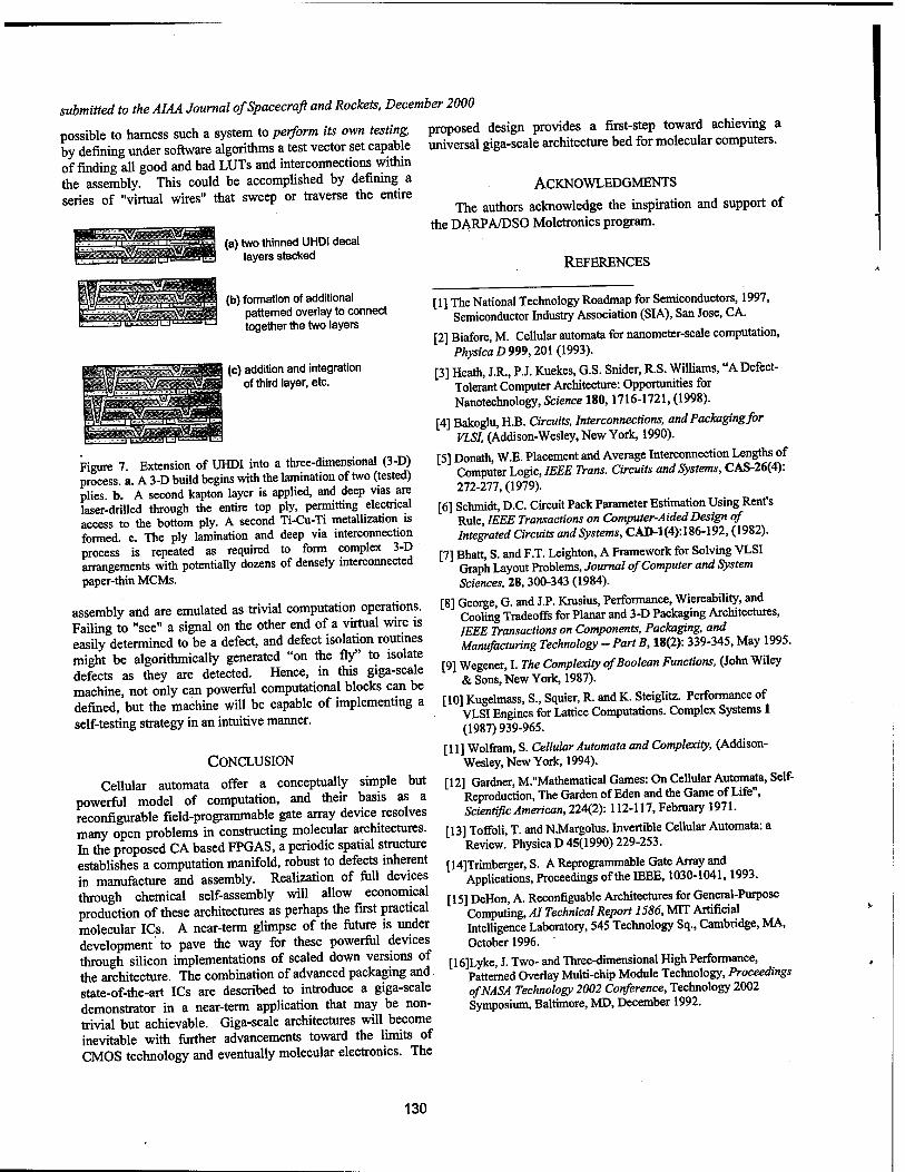
submitted to the AIM Journal of Spacecraft and Rockets, December 2000
possible to harness such a system to perform its own testing, by defining under software algorithms a test vector set capable of finding all good and bad LUTs and interconnections within the assembly. This could be accomplished by defining a series of "virtual wires" that sweep or traverse the entire
(a) two thinned UHDI decal layers stacked
proposed design provides a first-step toward achieving a universal giga-scale architecture bed for molecular computers.
ACKNOWLEDGMENTS
The authors acknowledge the inspiration and support of the DARPA/DSO Moletronics program.
REFERENCES
(b) formation of additional patterned overlay to connect together the two layers
(c) addition and integration of third layer, etc.
Figure 7. Extension of UHDI into a three-dimensional (3-D) process, a. A 3-D build begins with the lamination of two (tested) plies, b. A second kapton layer is applied, and deep vias are laser-drilled through the entire top ply, permitting electrical access to the bottom ply. A second Ti-Cu-Ti metallization is formed, c. The ply lamination and deep via interconnection process is repeated as required to form complex 3-D arrangements with potentially dozens of densely interconnected paper-thin MCMs.
assembly and are emulated as trivial computation operations. Failing to "see" a signal on the other end of a virtual wire is easily determined to be a defect, and defect isolation routines might be algorithmically generated "on the fly" to isolate defects as they are detected. Hence, in this giga-scale machine, not only can powerful computational blocks can be defined, but the machine will be capable of implementing a self-testing strategy in an intuitive manner.
CONCLUSION
Cellular automata offer a conceptually simple but powerful model of computation, and their basis as a reconfigurable field-programmable gate array device resolves many open problems in constructing molecular architectures. In the proposed CA based FPGAS, a periodic spatial structure establishes a computation manifold, robust to defects inherent in manufacture and assembly. Realization of full devices through chemical self-assembly will allow economical production of these architectures as perhaps the first practical molecular ICs. A near-term glimpse of the future is under development to pave the way for these powerful devices through silicon implementations of scaled down versions of the architecture. The combination of advanced packaging and state-of-the-art ICs are described to introduce a giga-scale demonstrator in a near-term application that may be non- trivial but achievable. Giga-scale architectures will become inevitable with further advancements toward the limits of CMOS technology and eventually molecular electronics. The
[1] The National Technology Roadmap for Semiconductors, 1997, Semiconductor Industry Association (SIA), San Jose, CA.
[2] Biafore, M. Cellular automata for nanometer-scale computation, Physica 0999,201(1993).
[3] Heath, J.R., P.J. Kuekes, G.S. Snider, R.S. Williams, "A Defect- Tolerant Computer Architecture: Opportunities for Nanotechnology, Science 180,1716-1721,(1998).
[4] Bakoglu, H.B. Circuits, Interconnections, and Packaging for VLSI, (Addison-Wesley, New York, 1990).
[5] Donath, W.E. Placement and Average Interconnection Lengths of Computer Logic, IEEE Trans. Circuits and Systems, CAS-26(4): 272-277, (1979).
[6] Schmidt, D.C. Circuit Pack Parameter Estimation Using Rent's Rule IEEE Transactions on Computer-Aided Design of Integrated Circuits and Systems, CAD-1(4):186-192, (1982).
[7] Bhatt, S. and F.T. Leighton, A Framework for Solving VLSI Graph Layout Problems, Journal of Computer and System Sciences, 28, 300-343 (1984).
[8] George, G. and J.P. Krusius, Performance, Wiereability, and Cooling Tradeoffs for Planar and 3-D Packaging Architectures, IEEE Transactions on Components, Packaging, and Manufacturing Technology - Part B, 18(2): 339-345, May 1995.
[9] Wegener, I. The Complexity of Boolean Functions, (John Wiley & Sons, New York, 1987).
[10] Kugelmass, S., Squier, R. and K. Steiglitz. Performance of VLSI Engines for Lattice Computations. Complex Systems 1 (1987) 939-965.
[11] Wolfram, S. Cellular Automata and Complexity, (Addison- Wesley, New York, 1994).
[12] Gardner, M."Mathematical Games: On Cellular Automata, Self- Reproduction, The Garden of Eden and the Game of Life", Scientific American, 224(2): 112-117, February 1971.
[13] Toffoli, T. and N.Margolus. Invertible Cellular Automata: a Review. Physica D 45(1990) 229-253.
[14]Trimberger, S. A Reprogrammable Gate Array and Applications, Proceedings of the IEEE, 1030-1041,1993.
[15] DeHon, A. Reconfiguable Architectures for General-Purpose Computing, AI Technical Report 1586, MIT Artificial Intelligence Laboratory, 545 Technology Sq., Cambridge, MA, October 1996.
[16]Lyke, J. Two- and Three-dimensional High Performance, Patterned Overlay Multi-chip Module Technology, Proceedings of NASA Technology 2002 Conference, Technology 2002 Symposium, Baltimore, MD, December 1992.
130

DISTRIBUTION LIST
DTIC/OCP 8725 John J. Kingman Rd, Suite 0944 Ft Belvoir, VA 22060-6218 1 cy
AFSAA/SAM 1570 Air Force Pentagon Washington, DC 20330-1570 1 cy
AFRL/VSIL KirtlandAFB,NM 87117-5776 2cys
AFRL/VSIH Kirüand AFB, NM 87117-5776 1 cy
AFRL/VSSE Kirüand AFB, NM 87117-5776 3 cys
Official Record Copy AFRL/VSSE l °y
131

132