unnnunmmnu - DTIC
90
AD A098 484 NAVAL POSTGRADUATE SCHOOL MONTEREY CA FIG 17/2.1 DIGITALLY TUNED AM/FM RADIO. (U) DEC 80 D OZOEMIR, N uALn IIHhhhhhllll' unnnunmmnu
-
Upload
khangminh22 -
Category
Documents
-
view
1 -
download
0
Transcript of unnnunmmnu - DTIC

AD A098 484 NAVAL POSTGRADUATE SCHOOL MONTEREY CA FIG 17/2.1DIGITALLY TUNED AM/FM RADIO. (U)
DEC 80 D OZOEMIR, N uALn
IIHhhhhhllll'unnnunmmnu

U• I2 125
11111 1.5 1 . 1111.
MICROCOPY RESOLUTION TEST CHART
NATIONAL BURLAU OF SIANDARDS 1963 A

00 NAVAL ADUATE SCHOOL0Monterey, California
" -.Q; "LECTEf1 'I2AY ~ &11
THESIS 'A DIGITALLY TUNED AM/FM RADIO
by
Dogan Ozdemir
and
Nurettin Bal
December 1980
Approved for public release; distribution unlimited.
- -0

UNCLASSIFIEDISCURITY CLASSIICATION OF Tmm. PA4 (ft ae Ri46e
!~E aIP~ I DOCU ME TATIO04 PAE URFC m -nCWLLAr s
| i I. RElPO T NU N186 N a. O W A GJ[II ON WO 3. I M i 9NT CATA OG U W09R[
A Digitally Tuned AM/FM Radio* Master's ,ihesisi-! ' . c e n b " a 9 R D -
-. PeRFOaRuNI o. mEPOmT Nuueaft
7. AUTNOIWAV 1 C O T A T 00 GRANT NSiill eI )
I6Dogan/OzdemirNuretin al
. PI[XO N 4 O004NIZATION A NC A NDO A 004956 'o PN m [IlJ[T.P O l[ . TASK
Naval Postgraduate SchoolMonterey, California 93940
I. CONTROLLING OPFImC NAME AN ASSog8 It. eIP@RTWI
Naval Postgraduate School // De w 98PMonterey, California 93940 3. HUGEnOF PAGES
14. MONITORING AGEN"V NAME a Aoo6Ir9w 41/went Cho Ad16. Of1o) IS. SECURITY CLASL (f this e
Unclassified
I. C ASaIICATION/ OENGIAO01N
1S. DiSTNIGUTION STATtKiNT (41 WO XllPoff)
Approved for public release; distribution unlimited.
I?. DSTRIGUTION STATrM6NT (.W We obe 00 M to eeki. of EOamel - Rieav
I& SUPPL9NUTARV NOTES
I. 199V W@ASS (CK o an - MUafte .dem if ooeoar Ami 5ttP AV *1m mu
Frequency SynthesizerPhase-Locked Loop (PLL)Electronic ProgrammingVoltage Controlled Oscillator (VCO)
Ms ASTACT (0 010 # V m It 08004100F 0 0~0? IVNO"-006-)
This report describes the design and operation of arelatively economical, single crystal, frequency synthesizerhat generates the required local oscillator frequencies forommercial AM and FM broadcast receivers. Selection of aesired station is accomplished by electronic programmingsing pushbutton control. Fine tuning is not necessary.eceiver frequency drift is not significant because the local-
AN l, 7oUNCLASSIFIED .- li*7) / A1, SEOUITY CLMI FgCATION S Of ll ' P AR (MI Ra
- - - - ~- ~

UNCLASSIFIEDft 6V La.&MVIC&IeO 411V 'rues 060 e o@ Ianes
(20. ABSTRACT Continued)
'oscillator frequency is crystal controlled. Low-cost medium-scale integrated circuits and a large-scale integratedcircuit (LSI) are the building blocks of this synthesizer.
Frequency synthesis techniques, elements of the systemdesign and experimental results are also presented.
ior3G?A&I
C 7AB 0
_D 8.striblat 9fl/n
)vatlabilitY C045*- _Avail aneIt
3O17 2 UNCLASSIFIEDO1 1 %% 414-4401 *V~,V6.*IYUO tw PGOIMO bea.

Approved for public release; distribution unlimited.
A Digitally Tuned AM/FM Radio
by
Dogan OzdemirLieutenant, Turkish Navy
B.S.E.E., Naval Postgraduate School, 1980
and
Nurettin BalLieutenant, Turkish Navy
B.S.E.E., Naval Postgraduate School, 1980
Submitted in partial fulfillment of therequirements for the degree of
MASTER OF SCIENCE IN ELECTRICAL ENGINEERING
from the
NAVAL POSTGRADUATE SCHOOLDecember 1980
Authors
Approved by: 4. TrL4~;hesis Advisor
dSecond Reader
Dean of Sciende and Engineering
3
L --

IIABSTRACT
This report describes the design and operation of a
relatively economical, single crystal, frequency synthesizer
that generates the required local oscillator frequencies for
commercial AM and FM broadcast receivers. Selection of a
desired station is accomplished by electronic programming
using pushbutton control. Fine tuning is not necessary.
Receiver frequency drift is not significant because the
local oscillator frequency is crystal controlled. Low-cost
medium-scale integrated circuits and a large-scale
integrated circuit (LSI) are the building blocks of this
synthesizer.
Frequency synthesis techniques, elements of the system
design and experimental results are also presented.
4

ITABLE OF CONTENTS
I. INTRODUCTION ------------------------------- 12
A. OBJECTIVE ------------------------------ 12
B. BACKGROUND ----------------------------- 12
C. SUMMARY OF THE RESULTS ----------------- 14
II. FREQUENCY SYNTHESIS ------------------------ 16
A. FREQUENCY SYNTHESIS TECHNIQUES --------- 16
1. Incoherent Synthesis --------------- 16
2. Coherent Direct Synthesis ---------- 16
3. Coherent Indirect Synthesis -------- 17
a. Analog phase-locked loopsynthesis ---------------------- 18
b. Digital phase-locked loopsynthesis ---------------------- 18
B. AM/FM RADIO FREQUENCY SYNTHESIZERREQUIREMENTS --------------------------- 21
III. SYSTEM DESIGN ------------------------------ 23
A. CONSIDERATIONS LEADING TO A BLOCKDIAGRAM -------------------------------- 23
1. Reference Frequency ---------------- 23
2. Phase Detector --------------------- 25
3. Voltage Controlled Oscillator ------ 25
4. Lowpass Filter --------------------- 26
5. Programmable Divider --------------- 27
B. SUBSYSTEM DESIGN ----------------------- 29
1. Voltage Controlled Oscillator (VCO)- 29
5
a. AM VCO -- - - - -- - - - - -- 30
b. FM VCO --------------------------- 35
2. Reference Oscillator, PhaseDetector, Programmable Divider --- 38
3. Prescaler ---------------------------- 43
4. Lowpass Filter ----------------------- 43
4 . Station Programming Circuit ------- 4
a. Selection Switches ------------ 4
b. Switch Debouncing ------------- 4
c. Encoder -------------------------- 48
d. Shift Register and NAND Gate -- 48
e. Latches --------------------------5
f. Programmable Read OnlyMemory (PROM)---------------------50
g. BCD/7-Segment Decoder/Driversand Displays ------------------ 5
IV. SUMMARY OF OPERATION AND PERFORMANCECHARACTERISTICS------------------------------ 55
A. SYSTEM OPERATION------------------------ 5
B. EXPERIMENTAL RESULTS--------------------- 64
V. CONCLUSIONS----------------------------------- 75
APPENDIX A: DESIGN THEORY---------------------------7
LISTVF-RZZqMNCZS --------------------------------- 84
BIBLIOGRAPHY ----------------------------------------- 85
INITIAL DISTRIBUTION LIST ---------------------------- 86
6

I
LIST OF FIGURES
Figure No.
1. Analog Phase-Locked Loop Synthesis ---------- 19
2. Digital Phase-Locked Loop Synthesis --------- 20
3. Evolution of the Digital AM/FM FrequencySynthesizer --------------------------------- 24
4. Schematic Diagram of the AM VCO ------------- 31
5. The Transfer Characteristics of the AM VCO - 32
6. Diode Capacitance versus Reverse Voltage --- 33
7. Schematic Diagram of the FM VCO ------------- 36
8. The Transfer Characteristics of the FM VCO - 37
9. VCO Internal Noise -------------------------- 39
10. Loop Response to the VCO Noise -------------- 39
11. Block Diagram of the MM 55110 --------------- 40
12. Voltage-Phase Characteristic of the PhaseDetector ------------------------------------ 42
13. Divide-by-20 Prescaler Circuit -------------- 42
14. Normalized Transient Response of the Phase-Lag-Lead Filter ----------------------------- 45
15. Switch Debouncing Circuitry ----------------- 49
16. Timing Circuitry ---------------------------- 49
17. Timing Diagram for Circuitry of Fig. 16 ---- 51
18. The Encoder and Latch Circuitry ------------- 52
19. PROM Circuitry ------------------------------ 54
20. Complete Block Diagram of the PLLFrequency Synthesizer ----------------------- 56
7

21. Schematic Diagram of the Synthesizer -------- 57
22. Schematic Diagram of the ProgrammingCircuit ------------------------------------- 58
23. Schematic Diagram of the Display Circuit --- 59
24. Output of the Phase Detector at Lock -------- 61
25. Output of the AM VCO ------------------------ 62
26. Output of the FM VCO ----------------------- 63
27. Output of the MC 12012 shown in Fig. 13 65
28. Output of the MC 3060 shown in Fig. 13 ----- 65
29. Spectrum of the AM VCO Output --------------- 72
30. Spectrum of the FM VCO Output -------------- 73
31. The Breadboard System of the Synthesizer --- 76
Al. Basic Block Diagram of the Phase-LockedLoop --------------------------------------- 79
A2. Phase-Lag-Lead Lowpass Filter --------------- 80
8

I
LIST OF SYMBOLS
f IN Programmable divider input frequency
f out Synthesizer output frequency
fref Reference frequency
Af Total frequency variation
t s Settling time
AGC Automatic gain control
AM Amplitude modulation
BCD Binary coded decimal
C0 Input capacitance of the MC 1648
CT Variable capacitance of the varactor diode
CMOS Complementary metal-oxide semiconductor
ECL Emitter coupled logic
FM Frequency modulation
Hex Hexadecimal
IC Integrated circuit
IF Intermediate frequency
Kd Gain constant of the phase detector
K0 Gain constant of the VCO
L Reference frequency division ratio
LO Local oscillator
LPF Lowpass filter
LSI Large-scale integrated circuit
M Variable modulus of the programmable counter
9

MSB Most significant bit
N Total division ratio
P Modulus of prescaler
PD Phase detector
PLL Phase-Locked loop
RF Radio frequency
PROM Programmable read only memory
TTL Transistor to transistor logic
T1 Filter coefficient of the lowpass filter
T2 Filter coefficient of the lowpass filter
VCO Voltage controlled oscillator
Damping ratio
Wi Input frequency to the PLL
w n Natural frequency
o 0 Output frequency of the PLL
Di(t) Input phase angle to the PLL
( t) Error phase angle of the PLLe
(Ct) Output phase angle of the PLL
10

ACKNOWLEDGEMENT
The authors wish to express their sincere appreciation
to Professor Glen A. Myers for his guidance and assistance.
3.l

I. INTRODUCTION
A. OBJECTIVE
Of interest is the design and construction of a frequency
synthesizer for a commercial AM/FM radio, which uses inte-
grated circuits to minimize size and cost and which provides
the user with precise and versatile electronic programming
of the desired station's frequency.
B. BACKGROUND
In conventional AM/FM radio receivers, it is necessary
to turn a knob for station or channel tuning. This
electromechanical system generates the appropriate frequency
of a local oscillator by means of an inductance-capacitance
oscillator. The problems involved in "knob-tuning" are:
1. Accurate tuning depends on the user's hearing
capability.
2. The output of a continuously tunable local oscillator
(LO) is subject to frequency drift which means occasional
retuning may be necessary.
Stable, rapid and accurate frequency selection is
available today using frequency synthesizers. In general,
all devices generating frequencies which are rational
multiples (or nearly rational multiples, in the case of
interpolation, etc.) of a standard input frequency are
12
....... lnl . .... ..... .Il~lll i I I I .. . " ' - ' ::A-i-

called frequency synthesizers, irrespective of the actual
frequency changing process involved.
The frequency synthesizer is a tunable oscillator
having exceptional qualities such as:
1. Long-term stability equal to that of one or a few
reference signals (which can be very stable).
2. Perfect resettability.
3. An extremely large frequency range (decade
synthesizers).
4. Incremental tuning independent of the value of the
output frequency.
Frequency synthesizers, therefore, function as oscil-
lators and in many respects perform better than continuously
tuned oscillators. An outstanding advantage of frequency
synthesizers, in these times of automation, is their
adaptability to remote and digital tuning and compatibility
with computer control.
Because they are able to generate a large number of
frequencies in a broad frequency band with considerable
precision, frequency synthesizers are used in many
measuring applications (frequency comparison, phase
measurement, etc.). And they form an indispensable part
of the instrumentation in standard frequency and time
laboratories.
In radio communications, the use of frequency synthe-
sizers in transmitters is a well established technique.
13

The introduction of digital synthesizers and integrated
circuit (IC) technology in the mid-1960's paved the way
for their widespread use in receivers. With the present
state of the art, use of a communications system in which
all the carrier and heterodyning frequencies used in the
transmitter and receiver are derived from primary (atomic)
standard is conceivable.
Today, many commercial television receivers have
pushbutton tuning which is possible through use of a
frequency synthesizer.
C. SUMMARY OF THE RESULTS
A frequency synthesizer having the following charac-
teristics was designed, built and tested.
(1) Tuning range: 955 kHz to 2055 kHz for AM
77.4 MHz to 97.2 MHz for FM
(2) Electronic tunable in 10 kHz steps (111 channels)
for AM and 200 kHz steps (100 channels) for FM.
(3) Frequency stability of + 30 Hz or 0.0042% for AM
and of ; 400 Hz or 0.00082% for FM.
(4) Spurious outputs better than -30 db for AM and
-48 db for FM.
(5) Estimated volume of final package that contains
3five LSI's is 75 cm,
(6) Estimated cost of the synthesizer in mass production
is $30.
14

Results of this research clearly show that a PLL, in
conjunction with a programmable divider, can be used as a
frequency synthesizer and maintain frequency stability.
15
. I

II. FREQUENCY SYNTHESIS
A. FREQUENCY SYNTHESIS TECHNIQUES
Frequency synthesis techniques can be identified as
either
1. Incoherent synthesis
2. Coherent direct synthesis
3. Coherent indirect synthesis
1. Incoherent Synthesis
Incoherent synthesis utilizes essentially the
method of successive heterodyning. The exact manner in
which output frequencies are generated from input fre-
quencies in incoherent synthesis varies depending on the
application. Output frequency range, value of the smallest
frequency increment, frequency stability and accuracy,
level of the spurious outputs, size, cost and power
consumption are factors governing the choice of design.
The main goal of this technique, though, remains the same
in all cases--to minimize the number of crystal and basic
building blocks such as oscillators, mixers, and filters.
2. Coherent Direct Synthesis
The main difference between incoherent and coherent
synthesis is the number of frequency sources utilized in
the process of frequency generation. In the incoherent
synthesis approach there are numerous crystal-controlled
16
.... .. . . . . . . . ... . . .' . .. . ... .I. . . .. . I ll lll lllll ... ... .. .. .l .. . . . ... . .. .I

oscillators; in the coherent direct synthesis approach,
only one reference source is used. Hence, the stability
and accuracy of the output frequency in this method are
the same as the stability and accuracy of the reference
source. This feature makes coherent direct synthesis
attractive.
3. Coherent Indirect Synthesis
Coherent indirect synthesis utilizes the principle
of feedback to generate frequencies in increments. The
technique, known as phase-locking, differs from coherent
direct synthesis in many respects. The system analysis
of coherent indirect synthesis centers on an investigation
of phase-locked loop (PLL) stability and acquisition.
Mixers, multipliers, dividers, and filters are used in
synthesis, but so also are voltage-controlled oscillators
(VCO's), programmable dividers, phase detectors and
frequency discriminators. The main problem associated
with coherent indirect synthesis techniques is dynamics
of the feedback network (loop stability and acquisition).
By providing small-size, light-weight equipment that
consumes little power, these techniques exhibit many
advantages not offered by coherent direct synthesis.
Coherent indirect synthesis techniques can be grouped as:
a. Analog phase-locked loop synthesis
b. Digital phase-locked loop synthesis
17

a. Analog phase-locked loop synthesis
Fig. 1 is a block diagram of an analog PLLx2
frequency synthesizer where the expression Z2 mf ref+Rm-x 1
describes an input signal with a high harmonic ontent.
The harmonics of the signal that are passed by the filter
one at a time are x1fref through X2fref* The rest of the
harmonics suppressed by the filter are denoted as R. The
frequency of the VCO, fout' is downconverted and compared
to the reference frequency, fref" When the difference
between these two frequencies is small, the phase detector
generates a slowly varying AC voltage, which is passed by
the lowpass filter, and pulls the VCO into lock. Under
locked condition, the output of the phase detector is a
DC voltage whose amplitude and polarity are determined by
the amount and direction of phase displacement between the
reference and downconverted VCO signals. The lowpass
filter (often a combination of a lowpass filter and lag-
lead network) changes the amplitude and phase of individual
signals passing through it as a function of the working
frequency to achieve stable loop performance.
b. Digital phase-locked loop synthesis
A technique which is of considerable current
interest is the digital phase-locked loop synthesis. The
basic form of a digital PLL is shown in Fig. 2. The loop
consists of a VCO, variable-ratio frequency divider, phase
comparator, and lowpass filter. The VCO output is divided
18

___________1_________
0
'444
* 10-4
z
E--4
I.In
194
-4 -

ccI
riz
C4
0*
20

.. .... .........
and compared with a stable reference. Error voltages
derived from the phase comparator maintain the VCO on
frequency. Frequency selection is accomplished by a
channel selector (the control panel), which varies the
division ratio of the frequency divider. For locking to
occur,
fout N • ref (2.1)
where N is an integer.
Eq. (2.1) indicates that the smallest frequency
increment generated by the loop is equal to the reference
frequency, fref" The important characteristics offered
by a digital PLL are small size and low DC power consump-
tion. At low frequencies, when slow-speed integrated
circuits are used, DC power drain is very small, making
the digital synthesizer suitable for battery operation.
B. AM/FM RADIO FREQUENCY SYNTHESIZER REQUIREMENTS
The synthesizer of interest must generate the required
local oscillator frequencies for AM and FM broadcast bands
which are about 88 MHz apart.
The AM broadcast band consists of channels 10 kHz wide
starting at 500 kHz. Therefore, the carrier for the first
channel is at 500 kHz, and the carrier for the last channel
is at 1600 kHz. The- receiver local oscillator must
generate frequencies separated by 455 kHz from the broadcast
21

frequencies to accommodate the receiver intermediate
frequency (IF) amplifier. Therefore, the local oscillator
frequencies required are 955 kHz to 2055 kHz with 10 kHz
channel spacing. A list of all the required frequencies
for all the stations in the AM broadcast band is a part
of Table I in section IV.A.
The FM broadcast band occupies 2 MHz between 88 MHz
and 108 MHz. There are 100 channels which are spaced
200 kHz apart. The carrier for the first channel is at
88.1 MHz and the last carrier for the last channel is
107.9 MHz. Again, to keep the IF frequency at 10.7 MHz,
the local oscillator frequency should be 10.7 MHz from
the carrier frequency. If the lower band is chosen, the
local oscillator frequencies required are 77.4 MHz to
97.2 MHz with 200 kHz channel spacing. A list of all the
required frequencies for all the stations in the FM
broadcast band is a part of Table II in section IV.A.
22

III. SYSTEM DESIGN
A. CONSIDERATIONS LEADING TO A BLOCK DIAGRAM
It is first necessary to choose the proper technique
for the desired frequency synthesizer among the frequency
synthesis techniques mentioned in Chapter I. Initially,
the techniques which utilize a single reference source were
considered, in order to rely on the stability and accuracy
of a single crystal oscillator. Between the choices of
direct synthesis and coherent indirect synthesis, both of
which met initial requirement, the latter was chosen because
of its advantages such as phase noise, switching speed, fre-
quency increments, small size and light weight (Ref. 11.
Once the PLL technique is chosen, the question of having
a single loop for both AM and FM bands arises. In that case,
every part of the PLL loop shown in Fig. 3 is to function
in the same way for AM and FM, under the constraint of
operating in two different frequency bands which are about
88 MHz apart. The problems associated with the frequency
requirement are discussed in the following paragraphs for
all the parts of the loop.
1. Reference Frequency
As pointed out in section II.A.3.b of this report,
in order for locking to occur,
fout = N f ref (2.1)
23
LS

DETECTOR -- FLE C
PROGRAM-MABLE
(b)
Fig.~~~~~~~ 3.t' EVLUIO OFTEDGTLA/FrRQECYTeIE
f ref HASE OWP 24
D E E T R I T R N

which means that frequencies may be generated which are
integer multiples of the reference frequency. Hence, the
same reference frequency should be able to generate the
AM and FM local oscillator frequencies. A 5 kHz frequency
is the largest possible reference which will generate the
AM local oscillator frequencies from 955 kHz to 2055 kHz
with 10 kHz channel spacing and the FM local oscillator
frequencies from 77.4 MHz to 97.2 MHz with 200 kHz channel
spacing. This is so because 5 kHz is the least common integer
factor of 955 kHz, 965 kHz ... 2055 kHz.
2. Phase Detector
Phase comparison is accomplished at a reference
frequency fref" There are many reasons for making the phase
detector frequency as large as possible. Phase noise,
switching tiiae, and spurious frequency modulation (FM) at
fref are among the most important considerations (Ref. 11.
Group loop currents, which present a problem below approxi-
mately 5 kHz, are another reason for making fref large.
In the design of this particular synthesizer, the
largest possible reference frequency of 100 kHz for FM was
lowered to the largest reference frequency of 5 kHz for AM
to utilize the same phase detector as shown in Fig. 3b.
3. Voltage Controlled C cillator (VCO)
The most severe constraint on the single loop AM/
FM frequency synthesizer is the VCO due to its tuning range
and linearity. If a single VCO were to be used in the loop,
it would require linear operation over a 100 MHz tuning
25

range. Such a VCO would have a conversion gain of 107 Hz/volt
where
K0 = Conversion Gain = r ion0 Control voltage range that providesthe linear operation
1 i00 MHz 710 V (Assumed) = 10 Hz/volt
This means that the control voltage step required between
any two adjacent channels in A14 would be 10- voltes which
is very difficult to control. There are two ways to have
different tuning ranges for each broadcast band--by elec-
tronic switching of the elements of the VCO or by using two
separate VCO's. It was decided to use two VCO's because
of circuit simplicity and reliability of operation. The
synthesizer involving two VCO's is shown in Fig. 3b.
4. Lowpass Filter
The transient performance and the frequency response
of the PLL is dependent upon the phase detector conversion
gain Kd, the VCO conversion gain K0 and the choice of the
filter (Ref. 2]. As shown in Fig. 3b, there is one phase
detector and there are two VCO's with different conversion
gains K0 (AM), K0 (FM). What happens in the performance of
the loop with two separate K0 's is that one of the two
calculations using each K0 gives poorer performance for the
loop. The K0 which causes that performance is taken into
account in determining the elements of the loop filter which
are considered in section B.4 of this chapter.
26

S. Programmable Divider
The required division ratios, to achieve the AM and
FM local oscillator frequencies using a 5 kHz reference
frequency, are given below:
AM: Local oscillator frequencies = 955 kHz to 2055 kHz
Division ratios = 191 to 411
FM: Local oscillator frequencies = 77.4 MHz to 97.2 MHz
Division ratios = 15,480 tO 19,940
The maximum division ratio is less than 215. Using four
four-bit programmable dividers, division by any integer up
to 216 is possible. Hence, the desired division ratios are
easy to implement, providing programmable frequency dividers
are available at frequencies up to 100 MHz. Since this is
not the case, then for FM it is necessary to down convert
the signal between the FM VCO and programmable dividers.
The approach to down conversion used here is prescaling of
the FM VCO output frequency by a fixed high speed divider
until the programmable divider range is reached. In this
project, frequency division by P = 20 is used to keep the
200 kHz channel spacing compatible with the 10 kHz AM channel
spacing. The block diagram of the synthesizer design at this
point is shown in Fig. 3c.
6. Construction and Operation
The required reference frequency is 5 kHz. Since
the crystal oscillator design is somewhat difficult and
expensive at low frequencies, a high frequency crystal
27

f outMfref
- fr e f
-ref PHASE LOWPASS
PANEL
z:DETECTOR FILTER -put oMPf ref
Nf ref; FM VCO
"M _
RO GRAM -
MABLE I FIXEDQ
f ref foutMPf2re8AM VCOl FM V C 0
FIXED
REF.O"C L
LOWPASS PHASE "M. i RO G RAM -
FILTER DET. I MALE F
I ONTROL
PANEL
(d)
Fig. 3. EVOLUTION OF THE DIGITAL AM/FM FREQUENCY SYNTHESIZER
28

oscillator followed by a divider circuit should be used.
In order to generate the reference signal to be used in
the phase detector, the output of the crystal oscillator
is divided by L.
The next step in the design of the PLL is selection
of the specific IC's. After all of the available PLL inte-
grated circuits were taken into consideration, only a large-
scale integrated circuit (LSI), which contained a reference
oscillator, a reference frequency divider, a phase detector,
and a programmable divider, was chosen because of its rela-
tively small size and low cost.
The design of the electronic programming part of
the system is a straightforWard digital process whereby a
column of channel selection switches set by the operator
controls the programmable divider.
Design and circuit of each part of the system are
given in the next section.
B. SUBSYSTEM DESIGN
In this section the design and performance of the sub-
systems of the digitally tuned AM/FM radio synthesizer of
Fig. 3d are presented.
1. Voltage Controlled Oscillator (VCO)
The MC 1648 is an emitter-coupled oscillator, con-
structed on a single monolithic silicon chip. The oscillator
requires an external parallel tank circuit consisting of
an inductor (L) and capacitor (C).
29

A varactor diode, Motorola MV 1404, is incorporated
into the tank circuit to provide a voltage variable input
for the oscillator. The connection of the varactor diode
and other circuitry external to the MC 1648 differs for the
AM VCO and FM VCO.
a. AM VCO
Fig. 4 is the schematic diagram, and Fig. 5 is
the transfer characteristic of the AM VCO. The VCO is in-
tended to operate from 955 kHz to 2055 kHz. The actual
operating range has to be determined by considering the worst
case transition from one frequency to another. In this de-
sign, an acceptable frequency overshoot of 25% was chosen.
This now places the AM frequency band for the LO in the
range 716 kHz to 2568 kHz.
The VCO design in the range of 716 kHz to
2568 kHz starts with the resonant frequency formula [Ref. 3]
f (3.1)
2,n VL_
In the VCO circuit of Fig. 4, the value of the
tank circuit capacitance C is C0 +CT where
CO = 6 pr, input capacitance of the MC 1648 and
CT = the varactor diode capacitance.
The value of CT changes according to the voltage applied.
Fig. 6 shows the variation of CT with voltage.
30

II
+5v
4.71a
1 14
10 3 - OUTPUT
O.;FL MC 1648T
v 7 o. luFVIN 0001UF
D : MV 1404 VARACTOR DIODE
L : ADJUSTABLE RF COIL (200UH-400UH)
Fig. 4. SCHEMATIC DIAGRAM OF THE AM VCO
31

OUTPUT FREQUENCY (MHz)2.2
2.0
1.8
1.6
1.4
1.2
1.1
1.0 V IN (VOLTS)
1.5 2.0 2.5 3.0 3.5 4.0 4.5 5.0 5.5 6.0
Fig. 5. THE TRANSFER CHARACTERISTIC OF THE AM VCO
32

700
3o33
-1 I

From Eq. (3.1),
LC -
where:
716 kHz < f < 2568 kHz.
Solution for LC gives
3.841 (mH)(pF) < LC < 49.402 (.aH)(pF).
Picking L - 0.3 mH gives
12.8 (pF) < C < 164.6 (pF)
6.8 (pF) < CT < 158.6 (pF)
The limits of the capacitance, CT, correspond to the reverse
bias voltage of the MV 1404 from 1 volt to 7.5 volts which
are found by means of the varactor diode's voltage-capaci-
tance characteristic (Fig. 6). To obtain a sine wave at
the output, a resistor is added from the AGC circuit (pin 5)
to ground (Fig. 4).
The conversion gain, K0, which is simply the
slope of the transfer characteristic, can be calculated as
K 2T(f 2 -f) 27r(2-1)x10 = 1,427,998 Rad/volt-sec.0 (V 2Vj 1 =
34
£

b. FM VCO
The schematic diagram and the transfer character-
istic of the FM VCO are shown in Fig. 7 and Fig. 8 respectively.
The frequency range is the only difference in
the design of the FM VCO from that of the AM VCO. The LO
frequency range for FM is 58.05 MHz to 121.5 MHz when 25%
overshoot values are included. From Eq. (3.1)
1LC 2
4Tr f
where:
58.05 MHz < f < 121.5 MHz.
Solution for LC gives
1.716 (iH) (pF) < LC < 7.516 (iH) (pF)
Picking L - 0.1 'pH gives
17.16 (pF) < C < 75.16 (pF)
11.16 (pF) < CT < 69.16 (pF)
From Fig. 6, it is necessary for the reverse bias voltage of
the varactor diodes to vary from 3.1 volts to 7.5 volts in
order to obtain CT within the limits given above. To extend
the useful frequency range of the device a i kohm resistor
is added to the AGC circuit at pin 5 as in Fig. 7.
35

+5V
0. IWF
1 14
10 3 OUTPUT
L MC 1648V IN 51
7N 12 1K-..._5 F 1 7 85 +5* V
"r . 1:1
D MV 1404 VARACTOR DIODE
L : MICRO METAL TOROIDAL CORE # T30-22
5 TURNS OF NO. 20 COPPER WIRE
Fig. 7. SCHEMATIC DIAGRAM OF THE FM VCO
36
4". .. ....

OUTPUT FREQUENCY (MHZ)
96
94
92
90
88
86
84
82
80
78 • IN (VOLTS)
5.8 5.9 6.0 6.1 6.2 6.3 6.4 6.5 6.6 6.7
Fig. 8. THE TRANSFER CHARACTERISTIC OF THE FM VCO
37

The conversion gain, K0 , is calculated from
Fig. 8 as:
2Tr ( f 2-f)K = 20 v2- v1
= 2r(92-82)xl06 = 116.3x10 6 Rad./volt-sec.6.56-6.02
There is a variation of the output frequency
due to internal noise of the MC 1648. The plot of this
variation is given in Fig. 9. The analysis of the frequency
response of the closed loop shows that the noise component
in the VCO above the loop natural frequency, wn' will pass
unattenuated and those below will have the same degree of
suppression as seen in Fig. 10. Therefore, the VCO internal
noise must be considered when the loop natural frequency is
chosen.
2. Reference Oscillator, Phase Detector, ProgrammableDivider
The PLL frequency synthesizer used in this project
is a monolithic metal gate CMOS integrated circuit identi-
fied as MM 55110. Fig. 11 shows the circuit functions and
pin connections. The device operates from a single power
supply and contains an oscillator with feedback resistor,
divider chian, a binary input programmable divider with con-
trol logic for transmit mode [. (M+91)] or receive mode
[.-44] and the necessary phase detector logic. (The device
can be used in double IF or single IF systems.)
38

I UI
10 vOiouSop%*A-rim FftsqupImc'r (mv4rJ
Fig. 9. VCO INTERNAL NOISE
r-7
1.01
L.OG FREQUEN'CY
Fig. 10. LOOP RESPONSE TO THE VCO NOISE
39

40
0 u .0 Lf E-4 0z
UE-
En r4 0 0 r r-4O
-4
0 E4
W E-4-0
~zE-4 04-4
H Hn
cno
4 z
H c 4
co 0 -4
+ E-4 0
cn40

The MM 55110 uses a 10.24 MHz quartz crystal to
determine the reference frequency, and it has a selectable
210 or 211 divider chain which gives either a 10 kHz or
5 kHz reference frequency. The selection of reference fre-
quency is made by use of the FS (Frequency Select) pin.
Signal level at pin 2 in Fig. 11 may be 1 volt peak-
to-peak. An internal amplifier adjusts the input signal
level to that required by the programmable divider circuit.
The divider circuit divides the input frequency by M < 1023
in the receive mode (M < 1114 in the transmit mode). Selec-
tion of M and hence station selection is accomplished by
mechanical switches or by external electronic programming
of the programmable divider which is done in this project
using a PROM (Programmable Read Only Memory).
Inputs to the programmable divider are binary sig-
nals having a high level above 6 volts. Operational ampli-
fiers were used to amplify the 4.3 volts high level voltage
of the PROM outputs to the 7.5 volts high level voltage of
the programmable divider inputs.
The phase detector output voltage is inversely re-
lated to the frequency of the input signal. This output
has a high impedance state when in the lock mode. The Lock
Detector output (LD) also goes to a high statae under lock
condition. From the phase detector's voltage-phase charac-
teristic shown as Fig. 12, the phase detector conversion
gain Kd is calculated as:
41

ltVCO (VOLTS)
•~ 7.19
PHASE
0.29 1 DIFFERENCE (RADS)
-2Tr 0 27
Fig. 12. VOLTAGE-PHASE CHARACTERISTIC OF THE PHASE DETECTOR
+5V
OUT 1 3 4 2 (4 + 10 20S C MC 12012 7 C
Q 3 C4 Q3 Q4 -MC 3060PROGRAMMABLE
DIVIDER
1o 0~5 102
Fig.. 13. DIVIDE-BY-20 PRESCALER CIRCUIT
42

d VH VL 7.19 - 0.29 = 0.549 volt/Rad.Kd - 4T 4 T"
3. Prescaler
An ECL integrated circuit chip MC 12012 and a TTL
integrated circuit chip MC 3060 (- 2 circuit) are used as
a fixed, divide-by-20 prescaler to accomplish the down con-
version of the FM VCO output to the range from 3.87 MHz to
4.68 MHz. The MC 12012 alone could have been used as a
fixed divide-by-10 prescaler, if the practical upper limit
(7 MHz) of the working range of the programmable divider
in the MM 55110 would have been close to its theoretical
limit 10.23 MHz. The prescaler circuit is shown in Fig. 13.
4. Lowpass Filter
As mentioned in Appendix A, the transfer function
of the loop filter used in this project is
1 + ST 2F(S) = (A-3)
1+ ST 1
The loop transient response, whose psecifications
are settling time and maximum overshoot, determine the filter
coefficient T1 and T2 . Reasonable values for the transient
response are assumed to be
Maximum overshoot < 25%
Settling time (ts) = 10 msec
Formulas developed in Appendix A are used to calculate the
filter elements R, R2 and C:
43

Kd K0 N 2R d + (A-12)
CN2 CKdK0 Cwnn
R - _ n C N (A-11)2 W CK dK 0
C = 2 N (A-13)R2 n R2KdK0
The values to be used in the above formulas are:
K0 = 1,427,998 Rad/volt-sec for the AM VCO
6K0 = 116.3x10 Rad/volt-sec for the FM VCO
K = 0.549 Volt/Rad
N = N = 411 for the AM loopmax
N = N = 19,440 for the FM loop~max
Wn are obtained from Fig. 14 using the response
specifications.
It is apparent that there are two different sets of
values (K0 ,N) to be used in the calculations of the filter
element values which should be the same for both of the loops.
The procedure uses filter element values calculated by
choosing K0 and N values for one loop. Then, these values
are used to determine the transient response (settling time
and maximum overshoot) of the other loop. A result is that
the AM loop provides slower response with higher overshoot
44

1.8
C..
SLS
0.0
0 6 a 10 1
Fig 147OMLZDTASIN EPNEO H
PHS-AGLA F. 0ILT-
8. 45

than the FM loop. Therefore, the worst-case design requires
use of the AM VCO conversion gain and maximum division ratio.
From Fig. 14 it is seen that a damping ratio ; = 0.8
will produce a peak overshoot less than 25% and will settle
to within 5% at wnts = 4.6 radians. Since the required
settling time (t s)is 10 msec, then the natural frequency
(W ) isn
nt s 4.6 460 Rad/secn t - 0.01=s
With assumed R = 10 kohm, solving Eqs. (A.12) and (A.13)
for R1 and C gives
R1 = 20.5 kohm
C = 0.2954 F
To check if the calculated filter elements above
satisfy the transient response for the FM loop, we first
solve Eqs. (A.7) and (A.8) for wn and ; to obtain
= 603 Rad/sec
= 0.983.
Then, from Fig. 14, the
Maximum overshoot = 18%
Settling time (ts) = 7.63 msec.
46
i

Obviously, the initial requirements of the transient
response are met also for the FM loop.
5. Station Progranming Circuit
As mentioned in the specifications of the MM 55110,
selection of a channel can be accomplished by external
electronic programming of the programmable divider. The
main consideration in designing the programming circuitry
is to obtain a fast and correct response from the channel
selection switches with a division number provided at the
inputs of the MM 55110. The station programming circuitry
consists of six parts.
a. Selection Switches
Switches provide appropriate logic levels to
IC's for the desired loop (AM and FM) and channel number.
An array of ten pushbutton switches represents the decimal
numbers 0 through 9. Selection of one channel from the
100 possible channels in FM or ll channels in AM is accom-
plished by first resetting the channel to 000 with the push-
button station reset switch, and then by pressing in sequence
the pushbutton switches representing the digits of the de-
sired 3 digit channel number. For example, to select station
59, press switch labeled 0, then that labeled 5 and then the
one labeled 9. An AM/FM switch selects either the AM or the
FM loop.
b. Switch Debouncing
Unpredictable outputs of the switches due to
switch bouncing are avoided by using RS latches to debounce
47

the switches electronically. Each time a switch gets pressed,
the debouncing circuit gives only one high-to-low pulse to
the encoder. The RS latch debouncing circuit is shown in
Fig. 15.
c. Encoder
The encoder transforms the decimal value of the
channel selection switch to a four bit BCD number and passes
the 3 decimal digit channel number through 3 latches where
it is used as an address to the PROM.
d. Shift Register and NAND Gate
To select the 3 digit channel number, the same
channel selection switches and the ecnoder are used three
consecutive times. After every digit, the output of the
encoder is stored in a different latch to allow the next
digit to be transferred to the encoder. Enabling only one
latch at a time is accomplished by the shift register and
the NAND gate. The NAND gate gets four inputs from the
encoder and one input from the channel selection switch "0".
Its output is the clock signal to the shift register. Also,
serial data to the shift register is always "1". The shift
register can be cleared by the station reset switch. The
enable lines to the latches are taken from the first three
outputs through inverters. Fig. 16 represents this circuitry.
First, the shift register is cleared and that enables all
the latches. Secondly, whenever one of the channel selection
switches is pressed, the NAND gate activates the shift register
48
LMi

+5V
SWITCH 7BCI OUTPUTTO THEENCODER
FROMSTAION +5V
F igNC .6.S IM ING CIRCUITRY
/49
740 40OMT0
ToTEELE S OF TH LACE
ROM4 STATIO THEQASE SWITCWICH"0
74g.16 TIMN 7C4430UFRMTRY
SE I L-----.9N O E
CLAINUT UPT

so that the data "l" is applied to the shift register.
Although the first decimal digit of a channel number is
taken as data to all altches, as soon as the switch is
released, the first latch retains the data while the others
are returning to the decimal digit "0". The next time, the
second and third latches take the second digit determined by
the pressed switch, but only the second latch holds the data.
Finally, the third digit is received by only the third latch.
Latch enabling order and the system timing diagram are shown
in Fig. 17.
e. Latches
Latches are used to hold the BCD value of each
channel number digit until another channel is selected.
The encoder and latch circuitry are shown in Fig. 18.
f. Programmable Read Only Memory (PROM--1024x8)
The PROM serves as a Table Look-up, and it has
the outputs of the latches as an address. It converts the
channel number in BCD to the corresponding division number.
The product of that number and the reference frequency is
the AM output frequency corresponding to that particular
channel number. In FM, the multiplication also includes the
fixed modulus P which is 20.
The channel numbers used for AM and FM are the
same. With the use of the same reference frequency, the
division numbers out of the PROM must be different for the
AM and FM frequencies. That distinction is achieved by
50
________________________

STATIONRESET
SERIAL
E
Fig. 1.7. TIMING DIAGRAM FOR CIRCUITRY OF FIG. 16
51

4>
-4
3 -4OD ---- a D 5-
CNq (4 4 j-4 In ut.0z
E -4 M~ 00 0
C44
In
52

applying "1" for FM and "0" for AM to the most significant
bit of the PROM address. That makes the first 512 addresses
available to AMand the second 512 addresses to FM. The
block diagram of the PROM (2708) is shown in Fig. 19.
g. BCD/7--Segment Decoder/Drivers and Displays
There are three docoder/driver and display groups.
They display the three digit channel number chosen by the
channel selection switches. The first display group is
designed in a way such that it can display either the digit
zero or one, which is all that is needed for the first digit
of the channel number. The second and third groups are
capable of displaying the numbers 0 through 9.
53

A4 0
0~
r-44
> x 0'
DQ 0' -
Q 1.0
oo
oT 00a
0: ~ -C
0 4
00CN U
54 1

IV. SUMMARY OF OPERATION AND PERFORMANCE CHARACTERISTICS
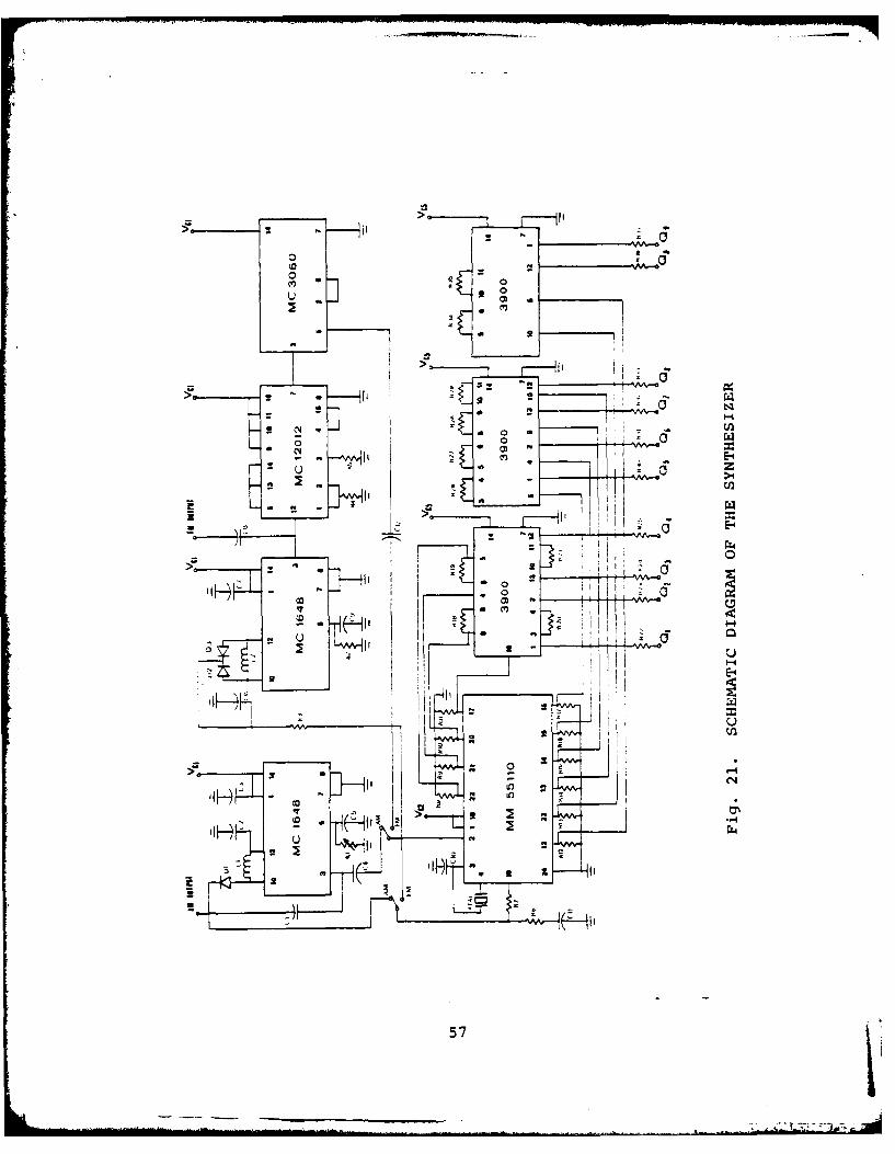
A. SYSTEM OPERATION
In this section, the operation of the synthesizer is
discussed. The subsystems are described in the preceding
chapter. Fig. 20 is a block diagram of the complete fre-
quency synthesizer with the programming circuit. Fig. 21
and Fig. 22 are the complete schematic diagrams of the syn-
thesizer and the programming circuit respectively.
In operation, programming the desired output frequency
is accomplished by setting the selection switches to the
appropriate channel number. The channel number is read
directly on the LED displays. Fig. 23 is a schematic dia-
gram of the display circuit. The variable division ratio N
is equal to M for AM and equal to M.P for FM.
The synthesizer loop oerates as follows. The phase
detector compares the phase of the input signal (f ) withref
that of the VCO signal divider output. The output voltage
of the phase detector, shwon in Fig. 24, passes through the
loop filter, which suppresses the high frequency components,
and then to the control element of the VCO which changes
its frequency in such a way that the phase difference be-
tween the input signal and the local oscillator output when
frequency divided by N is reduced. The synthesizer output
frequency is shown at various frequencies in Fig. 25 and
Fig. 26.
55

AM M
0 ~~- 10 R G A M N
Fig.20. OMPLTE LOCKDIAGAM O TH PLLFREQENCSYNTHSI ZE
RE56
E-4
57

-40
2 02
Itod
Sv
58

ILI -4
.44
in Uu $-4
mU
IILI
59

LIST OF COMPONENTS
R 5k C1 : 0.001 FR2 U1k C2 0.1 iF
R3 51 ki2 C3 : 4.7 1iF
R4 :500 S1 C4 : 0.001 iiF
R5 :500 Q C5 : 0-1iF
R 6 1 0 k Z C 6 5 LIFR6 10g6R 7 :20.5 kQ C 7 :0.1 pF
R8 through R17 :500 Q C a 0.001 ;F
R18 through R21 2 ki C9 0.1 pF
R 2 2 through R 2 5 1 ki C10 : 32 pF
R2 6 through R2 9 : 2 kQ C 0.3 4F
R 3 0 through R 3 3 : k D : MV 1404
R3 4 2 kQ D 2 MV 1404
R 3 5 : 2 k D 3 :MV 1404
R36 : 1 kU L1 : RF coil (200 iH-400 IiH)
R37 1 kU L2 Micro Metal ToraidalCore #T30-.22
R38 through R157 1.1 k 5 turns of #20 copperwire
R58 : 1ki
R59 1 kQ
60

Fig. 24. OUTPUT OF THE PHASE DETECTOR AT LOCK
(Ch. Ill AM, Horizontal: 0.1 ms/div.,Vertical: 2 V/div.)
61

Channel 001
Frequency = 955 kHz
Horizontal = 1 psec/div.
Vertical = 0.2 V/div.
Channel 055
Frequency = 1495 kHz
Horizontal = 1 vsec/div.
Vertical = 0.2 V/div.
Channel 110
Frequency = 2055 kHz
Horizontal = 1 4sec/div.
Vertical = 0.2 V/div.
Fig. 25. OUTPUT OF THE AM VCO
62

Channel 001
Frequency = 77.4 MHz
Horizontal = 0.01 psec/div.
Vertical = 0.5 V/div.
Channel 050Frequency = 87.2 MHz
Horizontal = 0.01 iisec/div.
Vertical = 0.5 V/div.
Channel 100
Frequency = 97.2 MHz
Horizontal = 0.01 psec/div.
Vertical = 0.5 V/div.
Fig. 26. OUTPUT OF THE FM VCO
63

The FM VCO signal at f is divided by a fixed modulusout
P and downconverted before it is applied to the variable-
ratio divider. This operation is shown in Fig. 27 and Fig. 28.
AM and FM station local oscillator (LO) frequencies are
given in Table I and Table II respectively.
B. EXPERIMENTAL RESULTS
The performance characteristics of the digital phase-
locked loop frequency synthesizer are summarized in Table III.
As shown in the output frequency section of Table III,
the output frequencies are off of the desired frequencies
in proportion to the accuracy of the center frequency of the
reference. However, that much difference does not cause
any problem in the IF amplifier bandwidths of 10 kHz for
AM and 200 kHz for FM. Stability of the output was deter-
mined only in short time intervals (less than two hours), and
was found to be ±30 Hz for AM and ±400 Hz for FM for the
breadboard circuit.
The second harmonic of the AM output frequency is 30 db
down from the fundamental as seen in Fig. 29. The presence
of this second harmonic can result in the reception of un-
desired strong stations especially in the first eight
channels (up to 1025 kHz). In conventional AM radio re-
ceivers, a radio frequency filter precedes the mixer. The
filter center frequency is shifted as the receiver is tuned
in order to avoid reception of "image" stations. Such radio
frequency filtering will also suppress reception of unintentional
64

Channel 001 FM
Frequency = 7.74 MHz
Horizontal = 0.1 isec/div.
Vertical = 1 V/div.
Fig. 27. OUTPUT OF THE MC 12012 SHOWN IN FIG. 13
Channel 001
Frequency = 3.87 MHz
Horizontal 0.1 -sec/div.
Vertical 2 V/div.
Fig. 28. OUTPUT OF THE MC 3060 SHOWN IN FIG. 13.
65

TABLE I
AM STATION LO FREQUENCY GENERATION
Table Contents:
A. Channel Number
B. Address to the PROM (Hex)
C. Memory Content (Hex)
D. Output Frequency (kHz)
A B C D A B C D
0 000 CF 2075 26 026 78 1205
1 001 5F 955 27 027 79 1215
2 002 60 965 28 028 7A 1225
3 003 61 975 29 029 7B 1235
4 004 62 985 30 030 7C 1245
5 005 63 995 31 031 7D 1255
6 006 64 1005 32 032 7E 1265
7 007 65 1015 33 033 7F 1275
8 008 66 1025 34 034 80 1285
9 009 67 1035 35 035 81 1295
10 010 68 1045 36 036 82 1305
11 011 69 1055 37 037 83 1315
12 012 6A 1065 38 038 84 1325
13 013 6B 1075 39 039 85 1335
14 014 6C 1085 40 040 86 1345
15 015 6D 1095 41 041 87 1355
16 016 6E 1105 42 042 88 1365
17 017 6F 1115 43 043 89 1375
18 018 70 1125 44 044 8A 1385
19 019 71 1135 45 045 8B 1395
20 020 72 1145 46 046 8C 1405
21 021 73 1155 47 047 8D 1415
22 022 74 1165 48 048 8E 1425
23 023 75 1175 49 049 8F 1435
24 024 76 1185 50 050 90 1445
25 025 77 1195 51 051 91 1455
66

TABLE I(Cont.)
A B C D A B C D
52 052 92 1465 78 078 AC 1725
53 053 93 1475 79 079 AD 1735
54 054 94 1485 80 080 AE 1745
55 055 95 1495 81 081 AF 1755
56 056 96 1505 82 082 BO 1765
57 057 97 1515 83 083 Bi 1775
58 058 98 1525 84 084 B2 1785
59 059 99 1535 85 085 B3 1795
60 060 9A 1545 86 086 B4 1805
61 061 9B 1555 87 087 B5 1815
62 062 9C 1565 88 088 B6 1825
63 063 9D 1575 89 089 B7 1835
64 064 9E 1585 90 090 B8 1845
65 065 9F 1595 91 091 B9 1855
66 066 AO 1606 92 092 BA 1865
67 067 Al 1615 93 093 BB 1875
68 068 A2 1626 94 094 BC 1885
69 069 A3 1635 95 095 BD 1895
70 070 A4 1645 96 096 BE 1905
71 071 A3 1655 97 097 BF 1915
72 072 A6 1665 98 098 CO 1925
73 073 A7 1675 99 099 Cl 1935
74 074 A8 1685 100 100 C2 1945
75 075 A9 1695 101 101 C3 1955
76 076 AA 1705 102 102 C4 1965
77 077 AB 1715 103 103 C5 1975
104 104 C6 1985
105 105 C7 1995
106 106 C8 2005
107 107 C9 2015
108 108 CA 2025
109 109 CB 2035
110 110 CC 2045
11 i1 CD 2055
67

TABLE II
FM STATION LO FREQUENCY GENERATION
Table Contents:
A. Channel Number
B. Address to the PROM (Hex)
C. Memory Content (Hex)
D. Output Frequency (MHz)
A B C D A B C D
0 200 82 77.2 25 225 9B 82.2
1 201 83 77.4 26 226 9C 82.4
2 202 84 77.6 27 227 9D 82.6
3 203 85 77.8 28 228 9E 82.8
4 204 86 78.0 29 229 9F 83.0
5 205 87 78.2 30 230 AO 83.2
6 206 88 78.4 31 231 Al 83.4
7 207 89 78.6 32 232 A2 83.6
8 208 8A 78.8 33 233 A3 83.8
9 209 8B 79.0 34 234 A4 84.0
10 210 8C 79.2 35 235 A5 84.2
ii 211 8D 79.4 36 236 A6 84.4
12 212 8E 79.6 37 237 A7 84.6
13 213 8F 79.8 38 238 A8 84.8
14 214 90 80.0 39 239 A9 85.0
15 215 91 80.2 40 240 AA 85.2
16 216 92 80.4 41 241 AB 85.4
17 217 93 80.6 42 242 AC 85.6
18 218 94 80.8 43 243 AD 85.819 219 95 81.0 44 244 AE 86.0
20 220 96 81.2 45 245 AF 86.2
21 221 97 81.4 46 246 BO 86.4
22 222 98 81.6 47 247 Bi 86.6
23 223 99 81.8 48 248 B2 86.8
24 224 9A 82.0 49 249 B3 87.0
68

TABLE II (Cont.)
A B C D A B C D
50 250 B4 87.2 76 276 CE 92.4
51 251 B5 87.4 77 277 CF 92.6
52 252 B6 87.6 78 278 DO 92.8
53 253 B7 87.8 79 279 Dl 93.0
54 254 B8 88.0 80 280 D2 93.2
55 255 B9 88.2 81 281 D3 93.4
56 256 BA 88.4 82 282 D4 93.6
57 257 BB 88.6 83 283 D5 93.8
58 258 BC 88.8 84 284 D6 94.0
59 259 BD 89.0 85 285 D7 94.2
60 260 BE 89.2 86 286 D8 94.4
61 261 BF 89.4 87 287 D9 94.6
62 262 CO 89.6 88 288 DA 94.8
63 263 Cl 89.8 89 289 DB 95.0
64 264 C2 90.0 90 290 DC 95.2
65 265 C3 90.2 91 291 DD 95.4
66 266 C4 90.4 92 292 DE 95.6
67 267 C5 90.6 93 293 DF 95.8
68 268 C6 90.8 94 294 EQ 96.0
69 269 C7 91.0 95 295 El 96.2
70 270 C8 91.2 96 296 E2 96.4
71 271 C9 91.4 97 297 E3 96.6
72 272 CA 91.6 98 298 E4 96.8
73 273 CB 91.8 99 299 ES 97.0
74 274 CC 92.0 100 300 E6 97.2
75 275 CD 92.2
69

TABLE III
CHARACTERISTICS OF THE SYNTHESIZER
Characteristics Remarks
1. Frequency Range: 1. Tunable in 10 kHz steps in
955 kHz to 2055 kHz (AM) AM and 200 kHz steps in
77.4 MHz to 97.2 MHz (FM) FM.
2. Frequency Selection: 2. The synthesizer is tuned
Electronically tuned by an electronic pro-
gramming circuit actuated
by pushbutton switches.
3. Output Waveform: 3. Output voltage (AM)> 0.8
Sine wave volts peak-to-peak
(Fig. 25) . Output
voltage (FM)> 1.5 volts
peak-to-peak (Fig. 26).
4. Reference Frequency: 4. Center frequency of the
fref = 5.00011 kHz crystal oscillator is
10.240255 MHz (measured).
The crystal temperature
coefficient is 10- 7
parts/C.
5. Output Frequency: 5. The AM output frequency
Ch.001 (A) = 955.321 kHz ± 20 Hz is given by:
Ch.055 (AM) = 1495.032 kHz ± 30 Hz fout = N x fref
Ch.lll (AM) = 2055.045 kHz ± 25 Hz = M x 5.0011 kHz
Ch.001 (EM) = 77.40169 MHz ± 300 Hz The FM output frequency
Ch.050 (FM) = 87.20197 MHz ± 350 Hz is given by:
Ch.100 (EM) = 97.20214 MHz ± 400 Hz ft = N x fout ref
= M x P x fref
= M x 20 x 5.00011 kHz
70
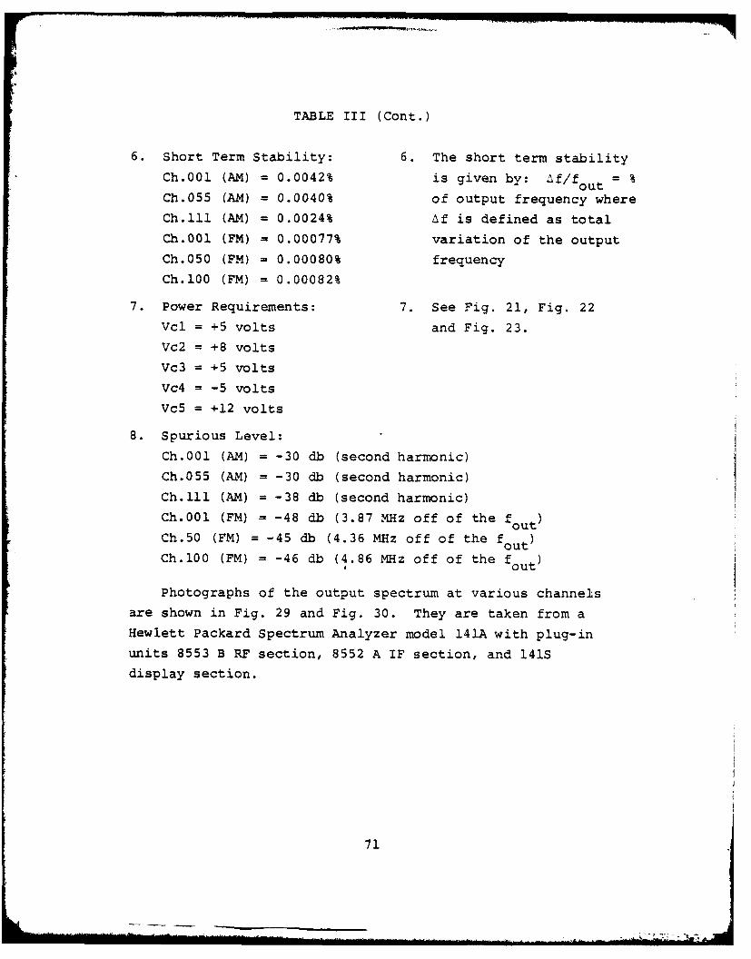
TABLE III (Cont.)
6. Short Term Stability: 6. The short term stability
Ch.001 (AM) = 0.0042% is given by: Af/fout = %
Ch.055 (AM) = 0.0040% of output frequency where
Ch.lll (AM) = 0.0024% Af is defined as total
Ch.001 (FM) = 0.00077% variation of the output
Ch.050 (FM) = 0.00080% frequency
Ch.100 (FM) = 0.00082%
7. Power Requirements: 7. See Fig. 21, Fig. 22
Vcl = +5 volts and Fig. 23.
Vc2 = +8 volts
Vc3 = +5 volts
Vc4 = -5 volts
Vc5 = +12 volts
8. Spurious Level:
Ch.001 (AM) = -30 db (second harmonic)
Ch.055 (AM) = -30 db (second harmonic)
Ch.lll (AM) = -38 db (second harmonic)
Ch.001 (FM) = -48 db (3.87 MHz off of the fOutCh.50 (FM) = -45 db (4.36 MHz off of the fout
Ch.100 (FM) = -46 db (4.86 MHz off of the fout
Photographs of the output spectrum at various channels
are shown in Fig. 29 and Fig. 30. They are taken from a
Hewlett Packard Spectrum Analyzer model 141A with plug-in
units 8553 B RF section, 8552 A IF section, and 141S
display section.
71

- Channel 001
Frequency = 955 kHz
Scan Width = 0.5 MHz/div.- Bandwidth = 100 kHzVertical = 10 db/div.
- Channel 055
Frequency = 1495 kHz
Scan Width =0.5 MHz/div.
Bandwidth = 100 kHz- Vertical = 10 db/div.
- Channel 110
Frequency = 2055 kHz
Scan Width = 0.5 MHz/div.- Bandwidth = 100 kHzVertical = 10 db/div.
Fig. 29. SPECTRUM OF THE ALM VCO OUTPUT
72

Channel 001
Frequency = 77.4 MHz
Scan Width = 2 MHz/div.
Bandwidth = 300 kHz
Vertical = 10 db/div.
Channel 050
Frequency = 87.2 MHz
Scan Width = 2 MHz/div.
Bandwidth = 300 kHz
Vertical = 10 db/div.
Channel 100
Frequency 97.2 MHz
Scan Width = 2 MHZ/div.
Bandwidth 300 kHz-Vertical = 10 db/div.
Fig. 30. SPECTRUM OF THE FM VCO
73

stations caused by the second harmonic of the frequency
synthesizer output.
In conventional AM radio receivers, to shift the center
frequency of the radio frequency (RF) filter, the capaci-
tance of the filter is varied by turning the shaft of the
tuning knob. In the receiver which utilizes a PLL frequency
synthesizer, the voltage out of the phase detector can
replace the tuning knob to provide a control voltage to
vary the capacitance or resistance of a radio frequency
filter.
74

V. CONCLUSIONS
The proposed design of the system was successfully
implemented. Individual blocks of the system were designed
and built on a breadboard. The AM and FM synthesizer
operated as intended. A picture of the breadboard system
is shown in Fig. 31.
The use of integrated circuits is important. These IC
chips provide for system portability due to their small
sizes and power requirements. The circuit power can be
supplied by batteries. The ruggedness of IC's reduces
susceptibility to damage, and their low cost keeps the
overall system price low. The VCO's have exceptional
stability, and the digital PLL provides a means of frequency
synthesis with a higher degree of stability than can be
obtained with the use of some other frequency synthesizers.
It was found that using an LSI chip was very useful,
because the reference frequency divider and the programmable
divider in the MM 55110 did not introduce phase noise into
the loop because they are contained in a shielded package.
The spurious outputs at the FM VCO output are caused
by interference from the output of the MC 3060 2 IC.
This interference can be reduced with shielding. Overall,
the fabrication of this synthesizer should have the following
features:
75

Fig. 31. THE BREADBOARDl SYSTEM OF THE SYNTHESIZER
76

(1) Shielding of internal circuits to prevent inter-
ference with other circuits and to prevent energy leakage
to the outside environment.
(2) Isolation of various circuit stages to prevent
undesirable feedback and coupling.
(3) Power line filtering to attenuate propagation of
RF signals.
(4) Using a separate ground bus for digital and analog
circuits.
(5) Well regulated power supplies with filtering
to remove AC signals from the power bus.
77

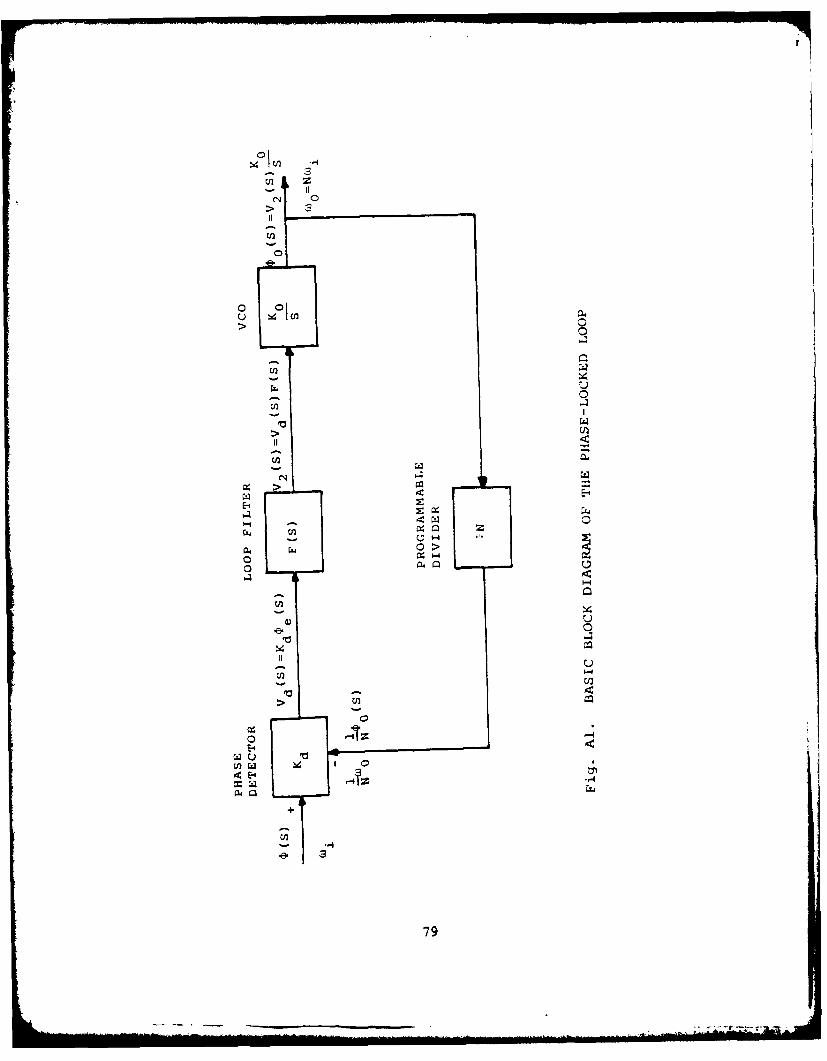
APPENDIX A
DESIGN THEORY
Basically, a digital frequency synthesizer is a frequency
source whose output is an integer multiple of an input
reference frequency. A phase-locked loop (PLL) circuit
provides stable operation. The basic components of a phase-
locked loop frequency synthesizer, shown schematically in
Fig. Al, are the voltage controlled oscillator (VCO), phase
detector (PD), lowpass filter and programmable divider.
In Fig. Al,
Kd = Conversion gain of the phase detector (Volts/Rad.)
K0 = Conversion gain of the VCO (Rad./Volts-sec)
Wi = Input signal frequency (Rad./sec)4i(S) = Input signal phase (Radians)
Pe(S) = Error signal phase (Radians)
.o 0 = Output signal frequency (Rad./sec)
D (S) = Output signal phase (Radians)o
F(S) = Transfer function of the loop filter
The transfer function of the system shown in Fig. Al
is
S(S) H(S) KOKdF (S) (A-)=~ H)= KoKd AlS +-NF (S)
N
78
ILi
(N'
>
MJ
,&
0
0
u0E4E -
u dlOH 0
79
i~~~ ~ ~~~~~~~~ iiz1.. ................ li"

Further,
e(S) S + KdKoF(S)[! -1](S)= 1 -H(S) = KdK0 N (A-2)
S + d0 F(S)N
Before proceeding further, it is necessary to specify
the loop filter F(S). Its task is to attenuate fast changes
in phase error due to noise in the input signal; it also
helps to smooth out the high-frequency components of the
phase detector output and feeds DC control voltage into VCO.
A high degree of attenuation on high frequency components is
possible by making the lowpass filter bandwidth narrow. The
narrow bandwidth also reduces the noise fed into the VCO,
resulting in a good spectral purity at the VCO output.
However, if the bandwidth becomes too small, the loop will
not be able to acquire lock. A trade-off should be done to
satisfy these conditions. In this project a phase-lag-lead
filter was used, as shown in Fig. A2.
__TIFig. A2. PHASE-LAG-LEAD LOWPASS FILTER
80 I

The transfer function of this filter is:
F(S) 1 +ST 1 (A-3)
where
T1 C(R1 + R2) (A-4)
T = CR 2 (A-5)
When substituting in Eq. (A-1), the loop transfer function
becomesKdK
(- -i (ST2 + 1)
H(S) = 2 1 K K (A-6)
S +-11,-+--T d T1 N 2 ]S+ NT1
Because the highest power of S in the derominator of the
transfer function is two, the loop is a second-order loop.
In this transfer function Kd and K0 are fixed numbers asso-
ciated with the phase detector and VCO, and N is variable
between Nmin and Nmax determined by the desired output fre-
quency. The system characteristics then will be determined
by the filter coefficients T1 and T2 as usual. Both wn'
natural frequency, and r, dampling factor, are particularly
important in determining the transient response and stability.
Comparing the denominator of the transfer function with the
normalized standard second-order characteristic equation,
$2 + 2 1hwnS + n' Wn and r can be found in terms of system
variables as:
81

W = VKdK0/NT1 (Rad./sec) (A-7)
= VN/TiKaKo[1 +T2 K d K0 (A- 8)
From Eq. (A-7) and Eq. (A-8), T1and T2are found to be:
KdKT d 0d (A-9)
1 NW 2n
T2 WI- N (A-i0)n dO0
In transient response, the desired overshoot and the
settling time between channels determine the damping ratio
and natural frequency respectively. Type two second-order
step response curves (Fig. 14) are used to spe,.ify w n~ and
~.Each response is plotted as a function of normalized
time w t. Once u) and ; are found, synthesis of the filtern n
is relatively straight-forward. Since T C(R +R ) and
o 2 CR2 from Eqs. (A-',) and (A-l), actual capacitor and
resistor values may be computed as:
R _2; N (A-1l)2 Cw CK dK 0
Td0+ N -2 (A-12)
R =K K CKICNw dO0 n
n
C = N N (A-13)2n R2Kd
82

In these equations, N = Nmax must be used, since it
represents the worst case (Maximum overshoot occurs at
Nmax which is minimum loop gain).
83

LIST OF REFERENCES
1. Manassewitsch, V., Frequency Synthesizer Theory andDesign, Wiley, 1976.
2. Signetics Corporation, Analog Applications Manual,Uniplar.
3. Motorola Semiconductor, Epicap Tuning Diode Theoryand Applications, Technical Information Note AN.178 A.
84

BIBLIOGRAPHY
Berlin, H.M., Design of Phase-Locked Loop Circuits withExperiments, Sams, 1978.
Gorski, Popiel, J., Frequency Synthesis: Techniques andApplications, IEEE, 1975.
Kroupa, V.F., Frequency Synthesis, Wiley, 1973.
Manassewitsch, V., Frequency Synthesizer Theory and Design,Wiley, 1976.
Motoryla Semiconductor, Epicap Tuning Diode Theory andApplications, Technical Information Note AN.178 A.
Motorola Semiconductor, MC 12012 Data Sheet.
Motorola Semiconductor, MC 1648 Data Sheet.
National Semiconductor, MM 55110 Data Sheet.
Signetics Corporation, Analog Applications Manual, Uniplar.
85

INITIAL DISTRIBUTION LIST
No. Copies
1. Defense Technical Information Center 2Cameron StationAlexandria, Virginia 22314
2. Library, Code 0142 2Naval Postgraduate SchoolMonterey, California 93940
3. Department Chairman, Code 52 2Department of Electrical EngineeringNaval Postgraduate SchoolMonterey, California 93940
4. Assoc. Professor G.A. Myers, Code 62Mv 10Department of Electrical EngineeringNaval Postgraduate SchoolMonterey, California 93940
5. Assoc. Professor G.D. Ewing, Code 62Ew 1Department of Electrical EngineeringNaval Postgraduate SchoolMonterey, California 93940
6. Deniz Yuzbasi Nurettin Bal 1Oyak Sitesi Blok: 36/8Yenilevent - Istanbul - TURKEY
7. Deniz Yizbasi Dogan Ozdemir 2Dr. Fazil G6kceoren Sok. Lale Apt.No: 20/7Gbztepe, Istanbul, TURKEY
8. Deniz Kuvvetleri Komutanlugi 2Egitim DairesiAnkara, TURKEY
9. Istanbul Teknik Universitesi 1Elektrik FakUltesiGUmUssuyu, Istanbul, TURKEY
10. Bogazici Universitesi IP. K. 2 Bebek, Istanbul, TURKEY
11. Orta Dogu Teknik Universitesi 1Ankara, TURKEY
86

- . -14