The Reconfigurable Instruction Cell Array
11
IEEE TRANSACTIONS ON VERY LARGE SCALE INTEGRATION (VLSI) SYSTEMS, VOL. 16, NO. 1, JANUARY 2008 75 The Reconfigurable Instruction Cell Array Sami Khawam, Ioannis Nousias, Mark Milward, Ying Yi, Mark Muir, and Tughrul Arslan Abstract—This paper presents a novel instruction cell-based re- configurable computing architecture for low-power applications, thereafter referred to as the reconfigurable instruction cell array (RICA). For the development of the RICA, a top-down software driven approach was taken and revealed as one of the key design decisions for a flexible, easy to program, low-power architecture. These features make RICA an architecture that inherently solves the main design requirements of modern low-power devices. Re- sults show that it delivers considerably less power consumption when compared to leading VLIW and low-power digital signal pro- cessors, but still maintaining their throughput performance. Index Terms—Dynamic reconfiguration, parallel processing, re- configurable computing. I. INTRODUCTION T HE NEED FOR new hardware architectures for future semiconductor devices was recognized several years ago as current architectures will not be able to cope with rising future requirements in data processing and throughput. Typical examples are mobile devices for next generation networks where a high amount of audio and video data will need to be processed. This adds extra burden on the processing elements in order to maintain a high throughput and stay efficient in terms of power-consumption and silicon costs. The hardware also needs to prove to be adaptable to upcoming standards. The four, equally important, requirements of such computing architectures are cost-reduction, short design time, low-power consumption, and high performance. Research into suitable ar- chitectures is an ongoing process, as a comprehensive solution capable of meeting all these requirements has yet to be found. To date there are several established ways in which algorithms can be implemented and run on silicon. Fig. 1 summarizes the merits and drawbacks of selecting a particular computation ar- chitecture in relation to each other. It is worthy to note that not a single architecture meets all the desired criteria, thus leaving room to consider other tradeoffs. Application-specific integrated circuits (ASICs) are well known to provide low power and high throughput compared to other architectures, however, their high design costs and limited post-fabrication flexibility means that they are only really feasible for large production count or for ultra low-power applications. CPUs are popular due to their ability to imple- ment designs after fabrication and their familarity to designers. Manuscript received May 10, 2006; revised May 30, 2007. S. Khawam, M. J. Milward, and M. Muir are with Spiral Gateway, Edinburgh EH9 3JL U.K. I. Nousias and T. Arslan are with the School of Engineering and Electronics, University of Edinburgh, Edinburgh EH9 3JL U.K., and also with Spiral Gateway, Edinburgh EH9 3JL U.K. Y. Yi is with the School of Engineering and Electronics, University of Edin- burgh, Edinburgh EH9 3JL U.K. Digital Object Identifier 10.1109/TVLSI.2007.912133 Fig. 1. Computation architecture tradeoffs. Over the years a number of techniques, such as several layers of cache, memory management, and branch prediction have been added to the CPU in order to keep the arithmetic logic unit (ALU) supplied with adequate instructions and data. This means that a diminishing proportion of the available silicon is actually used for the active computation. VLIW DSP archi- tectures offer advantages in terms of extra parallel processing. However, they are easily restricted by the limited amount of instruction level parallelism (ILP) found in typical programs. Field-programmable gate arrays (FPGAs) represent one pos- sible implementation of a range of reconfigurable computing devices. Their success lies in their ability to map algorithms onto their logic and interconnects after fabrication. This allows fabrication costs to be shared across many designs. While FPGAs provide the ability to map any logic functions on their fine-grained lattice, this has an impact on energy consump- tion since the majority of the available transistors are used to provide flexibility. Moreover designers are often required to have specialized skills in order to convert algorithms into a suitable register transfer level (RTL) code for synthesis. To achieve a suitable compromise of all design characteristics, designers develop custom system-on-chip (SoC) with a mixture of these architectures. To solve the problem of finding the ideal architecture, the research community has proposed many solutions based on the promise of high-performance offered by reconfigurable computing in terms of flexibility and a high amount of parallel processing. This includes architectures like Matrix, Garp, Elixent, PACT XAPP, SiliconHive, Montium, Pleiades, and Morphosys [2]–[9]. Even though these solutions achieve remarkable results in high computational-power and flexibility, they either do not provide enough power savings or are too difficult to program. 1063-8210/$25.00 © 2008 IEEE Authorized licensed use limited to: The University of Edinburgh. Downloaded on November 19, 2009 at 14:10 from IEEE Xplore. Restrictions apply.
Transcript of The Reconfigurable Instruction Cell Array

IEEE TRANSACTIONS ON VERY LARGE SCALE INTEGRATION (VLSI) SYSTEMS, VOL. 16, NO. 1, JANUARY 2008 75
The Reconfigurable Instruction Cell ArraySami Khawam, Ioannis Nousias, Mark Milward, Ying Yi, Mark Muir, and Tughrul Arslan
Abstract—This paper presents a novel instruction cell-based re-configurable computing architecture for low-power applications,thereafter referred to as the reconfigurable instruction cell array(RICA). For the development of the RICA, a top-down softwaredriven approach was taken and revealed as one of the key designdecisions for a flexible, easy to program, low-power architecture.These features make RICA an architecture that inherently solvesthe main design requirements of modern low-power devices. Re-sults show that it delivers considerably less power consumptionwhen compared to leading VLIW and low-power digital signal pro-cessors, but still maintaining their throughput performance.
Index Terms—Dynamic reconfiguration, parallel processing, re-configurable computing.
I. INTRODUCTION
THE NEED FOR new hardware architectures for futuresemiconductor devices was recognized several years ago
as current architectures will not be able to cope with risingfuture requirements in data processing and throughput. Typicalexamples are mobile devices for next generation networkswhere a high amount of audio and video data will need to beprocessed. This adds extra burden on the processing elementsin order to maintain a high throughput and stay efficient interms of power-consumption and silicon costs. The hardwarealso needs to prove to be adaptable to upcoming standards.The four, equally important, requirements of such computingarchitectures are cost-reduction, short design time, low-powerconsumption, and high performance. Research into suitable ar-chitectures is an ongoing process, as a comprehensive solutioncapable of meeting all these requirements has yet to be found.
To date there are several established ways in which algorithmscan be implemented and run on silicon. Fig. 1 summarizes themerits and drawbacks of selecting a particular computation ar-chitecture in relation to each other. It is worthy to note that nota single architecture meets all the desired criteria, thus leavingroom to consider other tradeoffs.
Application-specific integrated circuits (ASICs) are wellknown to provide low power and high throughput comparedto other architectures, however, their high design costs andlimited post-fabrication flexibility means that they are onlyreally feasible for large production count or for ultra low-powerapplications. CPUs are popular due to their ability to imple-ment designs after fabrication and their familarity to designers.
Manuscript received May 10, 2006; revised May 30, 2007.S. Khawam, M. J. Milward, and M. Muir are with Spiral Gateway, Edinburgh
EH9 3JL U.K.I. Nousias and T. Arslan are with the School of Engineering and Electronics,
University of Edinburgh, Edinburgh EH9 3JL U.K., and also with SpiralGateway, Edinburgh EH9 3JL U.K.
Y. Yi is with the School of Engineering and Electronics, University of Edin-burgh, Edinburgh EH9 3JL U.K.
Digital Object Identifier 10.1109/TVLSI.2007.912133
Fig. 1. Computation architecture tradeoffs.
Over the years a number of techniques, such as several layersof cache, memory management, and branch prediction havebeen added to the CPU in order to keep the arithmetic logicunit (ALU) supplied with adequate instructions and data. Thismeans that a diminishing proportion of the available siliconis actually used for the active computation. VLIW DSP archi-tectures offer advantages in terms of extra parallel processing.However, they are easily restricted by the limited amount ofinstruction level parallelism (ILP) found in typical programs.Field-programmable gate arrays (FPGAs) represent one pos-sible implementation of a range of reconfigurable computingdevices. Their success lies in their ability to map algorithmsonto their logic and interconnects after fabrication. This allowsfabrication costs to be shared across many designs. WhileFPGAs provide the ability to map any logic functions on theirfine-grained lattice, this has an impact on energy consump-tion since the majority of the available transistors are used toprovide flexibility. Moreover designers are often required tohave specialized skills in order to convert algorithms into asuitable register transfer level (RTL) code for synthesis. Toachieve a suitable compromise of all design characteristics,designers develop custom system-on-chip (SoC) with a mixtureof these architectures. To solve the problem of finding theideal architecture, the research community has proposed manysolutions based on the promise of high-performance offeredby reconfigurable computing in terms of flexibility and a highamount of parallel processing. This includes architectures likeMatrix, Garp, Elixent, PACT XAPP, SiliconHive, Montium,Pleiades, and Morphosys [2]–[9]. Even though these solutionsachieve remarkable results in high computational-power andflexibility, they either do not provide enough power savings orare too difficult to program.
1063-8210/$25.00 © 2008 IEEE
Authorized licensed use limited to: The University of Edinburgh. Downloaded on November 19, 2009 at 14:10 from IEEE Xplore. Restrictions apply.

76 IEEE TRANSACTIONS ON VERY LARGE SCALE INTEGRATION (VLSI) SYSTEMS, VOL. 16, NO. 1, JANUARY 2008
In this paper, we present and evaluate our novel reconfig-urable instruction cell architecture (RICA) that tries to specif-ically address all the desired requirements for future portabledevices. By designing the silicon fabric in a similar way to re-configurable arrays but with a closer equivalence to software,we achieve the same high performance as coarse-grain FPGAarchitectures and maintain the same flexibility, low cost, andprogrammability as digital signal processors (DSPs). The maindistinguishing and novel features of our reconfigurable architec-ture are as follows.
• An array of customizable instruction cells (ICs) that canbe dynamically reconfigured on every clock cycle enablingthe mapping of data-paths of both dependent and indepen-dent instructions.
• The reconfigurable core has ICs to deal with execution flowcontrol (conditional branches). Therefore, it does not re-quire coupling to a general purpose processor, since it pro-vides these features.
• The cell array configuration can be tailored towardsdifferent application domains, thus providing additionalpower optimizations and performance.
• A reconfiguration rate controller is provided to minimizethe impact of varying critical paths, which is an intrinsiccharacteristic of supporting dependent instructions
• The architecture is programmable with a high level lan-guage.
Consequently, a new dynamically reconfigurable system ispresented in this paper with its associated programming envi-ronment.
Section II of this paper covers related and previous work onreconfigurable computing architecture. Section III describes theRICA design along with descriptions of various key architec-tural design features. Section IV discusses some of the tech-niques used in the RICA to reduce power dissipation. Section Vcovers the tool-flow for programming RICA. Section VI coversthe evaluation of a sample RICA design. Finally, the conclusionis drawn in Section VII.
II. RELATED AND PREVIOUS WORK
Traditionally, algorithm functions are either statically real-ized in hardware (ASIC) or temporarily run on general-purposeprocessors (GPP). These two cases form the boundaries of alarge space of design exploration for possible ways of com-puting on silicon. The center ground of this space is filled byreconfigurable computing devices, with FPGAs being a well-known commercially successful example.
The concept of reconfigurable computing has been aroundsince the 1960s, when Estrin’s landmark paper proposed theconcept of a computer consisting of a standard processor andan array of “reconfigurable” hardware [1]. The main processorwould control the behavior of the reconfigurable hardware. Thereconfigurable hardware would then be physically tailored to aspecific task, such as image processing or pattern matching, withthe aim of running as quickly as a dedicated piece of hardware.Once the task was complete, the hardware could be manuallyadjusted to do some other tasks. This resulted in a hybrid com-puter structure aimed at combining the flexibility of software
with the speed of hardware. Unfortunately, this idea was wayahead of its time in terms of electronic technology.
In the last decade there has been a recent renaissance in thisarea of research with many proposed reconfigurable architec-tures developed both in industry and academia, such as Matrix,Garp, Elixent, PACT XAPP, SiliconHive, Montium, Pleiades,and Morphosys [2]–[9] to name but a few. These designs haveonly really become feasible by the relentless progress of silicontechnology, allowing for complex designs to be implementedonto a single chip. Nevertheless, the development of reconfig-urable hardware architecture is only one side of the problem,often overlooked is the importance of appropriate software toolsthat are essential for the programmability of the system andgaining the maximum performance. It is vital for reconfigurablesystems to be programmed from a common high-level language,as this enables complex algorithms to be quickly and effectivelytaken to the underlying architecture. To date, there is no clearclassification taxonomy for these developed reconfigurable sys-tems. However, they can be grouped together depending on var-ious architectural characteristics, such as the level of couplingwith a host processor, the logic granularity selected, the type ofinterconnect and topology and the rate of configuration and itsmanagement. Design decisions taken on one architectural as-pect greatly influences design decisions taken on others. For ex-ample, choosing a fine-grained logic granularity means that alarger amount of silicon is allocated to the interconnect for con-necting the logic together. This in turn impacts the rate it canreconfigure the device in real time due to the larger bitstreamsof instructions needed.
Several proposed reconfigurable systems combine a RISCprocessor with a coarse-grain reconfigurable array; some suchsystems are Morphosys, Garp, Elixent, and Pact XAPP. TheGarp reconfigurable architecture developed at the University ofCalifornia in 1997 involves a host processor that manages themain thread of control while certain loops or subroutines use areconfigurable array. The array is composed of rows of blocks,which have a resemblance to configurable logic blocks (CLBs)of a Xilinx FPGA. The blocks operate on 2-bit data. Vertical andhorizontal block-to-block wires provide data movement withinthe array, the interconnect only connects to its neighboringlogic blocks. Separate memory buses are provided to moveinformation in and out of the array. Each computation unit inthe Garp array can perform a logical or arithmetic operation onthe input 2-bit operands. Use of the array is controlled by themain processor. Host and reconfigurable array share the samememory hierarchy. Four memory buses are used to transferdata to and from the array. Other reconfigurable devices whichuse a reconfigurable array and processor coupling is Elixent,a start-up company based in Bristol, U.K., that was spun outfrom HP research labs. The reconfigurable array is based onthe D-fabrix consisting of a homogeneous grid of 4-bit ALUunits. To interface the core, an advanced microcontroller busarchitecture (AMBA) bus is used for programming the arrayand for transferring data to and from the host RISC. Eacharray has two high speed input/output (I/O) ports of 32 bits;these are divisible into multiples of 4 bits. The Morphosysreconfigurable computing project marries an on-board RISCprocessor with an array of reconfigurable cells. The Morphosys
Authorized licensed use limited to: The University of Edinburgh. Downloaded on November 19, 2009 at 14:10 from IEEE Xplore. Restrictions apply.

KHAWAM et al.: RECONFIGURABLE INSTRUCTION CELL ARRAY 77
architecture includes a reconfigurable processing unit, a GPP,and a high bandwidth memory interface. Each reconfigurablecell incorporates a 28-bit ALU, 16 12-bit multiplier, a shiftunit, a 16-bit input and 8-bit multiplexer, and 16-bit registerfile. In Pact’s XAPP array, the data-flow sections of algorithmsconsisting mostly of the pure arithmetic processing are mappedto the reconfigurable array. A microcontroller is utilized toload these code sections dynamically to the XAPP-array,which then processes these tasks. Data exchange between theXAPP, acting as coprocessor, and the microcontroller is donevia direct memory access (DMA) or shared memories. TheADRES architecture [11] closely couples the processor andreconfigurable fabric by sharing the memory and register-file;it tries to simplify the programming model through the use of ahigh-level C language. Nevertheless, the effect of this approachon area and power consumption was not measured.
The main decision why these systems have a separate pro-cessor and reconfigurable array is based on the observation thatsome code is “control flow” intensive, where there are a lot ofconditional branches to change program flow, while others partsof code contain highly parallel data paths, suitable for the re-configurable arrays. However, these systems suffer from diffi-culties in programming the arrays due to the use of specializedlow-level languages. They also suffer from limitations due to theloose coupling between the processors and the arrays, such ashow to allocate the program and large amounts of data-transfersbetween the array and processor.
Standalone coarse-grain reconfigurable arrays, such as thoseproposed earlier by Khawam et al. [10], provide good perfor-mance in area and power when compared to FPGAs, however,like FPGAs they require special hardware skills HDL to pro-gram them. RaPiD [12] is another one of these arrays, whereit utilizes a 1-D structure to take advantage of the fact that allof its functional components are word-width computational de-vices. One of the advantages of a 1-D structure is a reductionin complexity, especially in the communications network. An-other advantage is their ability to map systolic arrays very ef-ficiently, leveraging all of the research into the compilation ofalgorithms onto systolic arrays. Finally, while a 2-D RaPiD ispossible, most 2-D algorithms can be mapped onto a 1-D arraythrough the use of memory elements. To create different ver-sions of RaPiD that target different application domains, thefollowing changes need to be made to the array: modify ex-isting or add new functional units, change the width of the busesor the number of buses present, and modify the routing fabric.The RaPiD architecture can be programmed using the high-level RaPiD-C language but this language is not compatible withANSI-C and requires manual scheduling of parallel operations.
A fairly recent development in the reconfigurable arena isStretch’s [13] offering of a configurable processor with aninternal reconfigurable fabric. Stretch’s solution is capable ofdirectly compiling an application from C code. The softwaredeveloper identifies sections of code suitable for the reconfig-urable fabric using their profiling tool. This part of the C/C++source code can be compiled into configuration data for thereconfigurable fabric while the rest is run on the processor.This approach tries to solve the problem of communicationoverhead.
On the other side of the reconfigurable spectrum is themultiprocessors approach, where a sea of small processorsare connected through an interconnect network. Examplesof this are picoChip [14], Ambric [15], SiliconHive [6], etc.,and, to a lesser extent, the large CELL microprocessor withits eight fully-functional Synergistic processing elements (co-processors). PicoChip comprises of an array of heterogeneousindependent processors with a programmable communica-tion interconnect between the processors. Each processor isa 16-bit-wide RISC, with the inter-processor communicationprotocol based on a time-division multiplexing (TDM) scheme;data transfers between processor ports occur during time slotsand are scheduled at compile time, and controlled using the busswitches. The bus switch programming and the scheduling ofdata transfers is all fixed at compile time. Ambric concentrateson the interconnect structure and associated protocol. Ambricobjects communicate through a simple parallel structure ofhardware channels. Each channel is word-wide, unidirectional,point-to-point from one object to another, and acts like afirst-input–first-output (FIFO) buffer. Channels carry both dataand control tokens, in simple or structured messages. Channelhardware synchronizes its objects at each end dynamically asneeded at run time, not scheduled at compile time. Sending orreceiving a word on a channel is as simple as reading or writinga processor register. Since Ambric channels synchronize trans-parently and locally, the application achieves high performancewith none of that complex global synchronization. It is entirelyfeasible for the RICA to be the processors in the Ambric design.
III. RICA ARCHITECTURE
This section starts with a demonstrative example to allow aneasier understanding of the basic concept behind the architec-ture and then explains the structural elements of RICA.
A. Parallel Processing Example
The sample C code shown in Table I requires 19 cycles toexecute on a typical sequential processor. However, if the samecode is compiled for a VLIW DSP, such as the TI C6203, then itwould execute in 15 cycles, since the VLIW architecture wouldtry to concurrently execute up to eight independent instructions(six ALUs and two multipliers are available) [16]. If four si-multaneous multiplications and four memory accesses were per-mitted, then the number of cycles would reduce to eight. This isstill a long time considering the simplicity of the code and com-pared to what is achievable in hardwired solutions like FPGAs.The presence of dependent instructions, i.e., operations whichare dependent on previous operations, prevents the compilerfrom achieving further reductions in the number of clock cy-cles. We can observe that if the hardware architecture supportsthe mapping of both dependent and independent datapaths, thenwe could execute a big block of instructions in a single clockcycle without limitation.
We could easily execute the previous C code in only two cy-cles if the architecture provided 14 operational elements thatcan execute 4 ADD, 4 RAM, 4 MUL, and 2 REG si-multaneously, as shown in Fig. 2. This overcomes the limita-tion faced by VLIW processors and enables a higher degree ofparallel processing. As shown in Cycle 1 in Fig. 2, the longest
Authorized licensed use limited to: The University of Edinburgh. Downloaded on November 19, 2009 at 14:10 from IEEE Xplore. Restrictions apply.

78 IEEE TRANSACTIONS ON VERY LARGE SCALE INTEGRATION (VLSI) SYSTEMS, VOL. 16, NO. 1, JANUARY 2008
TABLE IEXAMPLE C-CODE AND ITS ASSEMBLED SEQUENTIAL AND VLIW CODE
COMPILED WITH LEVEL-2 OPTIMIZATIONS
Fig. 2. Execution of the 19 instructions in two cycles if the following parallelresources are available: 4�MUL, 4�ADD, 4�RAM, and 6�REG. The RICAprovides a heterogeneous array of instruction cells to map such steps.
delay-path is equivalent to two RAM accesses, one multiplica-tion, and some simple arithmetic operations. This is not muchlonger than critical paths in typical DSPs when compared to thegreater amount of instructions executed in parallel. Therefore,
Fig. 3. Harvard-like structure of the RICA architecture. The reconfigurablecore is composed of ICs and a network of programmable interconnects.
an architecture that supports such an arrangement might be ableto achieve similar throughputs as VLIWs but at a lower clockfrequency, depending on the type of computation.
B. RICA Reconfigurable Core
With the lessons learned from other reconfigurable fabrics,the RICA architecture has been purposely developed to handleboth control and dataflow aspects of the algorithms, along withbeing able to be programmed from industrial standard program-ming languages such as ANSI-C, on a high performance dy-namically reconfigurable fabric. The concept behind the RICAarchitecture is to provide a dynamically reconfigurable fabricthat allows building circuits such as the ones described in Fig. 2.By providing hardware modules that can execute assembly-likeinstructions similar to those in Fig. 2, a straightforward andCPU-like design-flow can be easily obtained. In the RICA ar-chitecture, these hardware modules are the named ICs. Havingan array of interconnectable ICs allows building circuits froman assembly representation of programs. The software is thenexecuted in multiple steps, where each step is a datapath of bothdependent and independent assembly instructions.
The ICs are interconnected through a network of pro-grammable switches to allow the creation of datapaths. In asimilar way to a CPU architecture, the configuration of theICs and interconnects are changeable on every cycle to exe-cute different blocks of instructions. As shown in Fig. 3, theprocessing data-path of RICA is a reconfigurable array of ICs,where the program memory contains the configuration bits (i.e.,instructions) that control both the ICs and the switches of theinterconnects. Special ICs in the core provide the interface tothe data and program memories.
Although the RICA architecture is similar to a CPU, the useof an IC-based reconfigurable core as a data path gives impor-tant advantages over DSP and VLIWs, such as better support forparallel processing. The reconfigurable core can execute a blockcontaining both independent and dependent assembly instruc-tions in the same clock cycle, which prevents the dependent in-structions from limiting the amount of ILP in the program. Otherimprovements over DSP architectures include reduced memoryaccess by eliminating the centralized register file and the use ofdistributed memory elements to allow parallel register access.
Authorized licensed use limited to: The University of Edinburgh. Downloaded on November 19, 2009 at 14:10 from IEEE Xplore. Restrictions apply.
KHAWAM et al.: RECONFIGURABLE INSTRUCTION CELL ARRAY 79
TABLE IIICS AND THEIR OPERATIONS
The characteristics of the RICA core are that it is able tobe fully customizable at design time and can be set accordingto the application’s requirements. This includes options suchas the bitwidth of the system and the flexibility of the array,which is set by the choice of ICs and interconnects deployed.These parameters also affect the extent of parallelism that canbe achieved and device characteristics such as area, maximumthroughput, and power consumption. Once a chip containing aRICA core has been fabricated, the system can be easily repro-grammed to execute any code in a similar way to a GPP.
C. ICs
In contrast to other reconfigurable architectures like [3], [4]the IC-array in the RICA is heterogeneous and each cell islimited to a small number of operations as listed in Table II.The cells are not restricted to the primitive operations shownin Table II, although the use of primitive cells compared tomultipurpose ALUs can potentially give a higher silicon uti-lization, since an ALU does not use all of its silicon estate atthe same time. Limiting the cells to such simple operations alsoreduces the number of I/O pins required for each cell (theseare typically two inputs and one output as in simple assemblyinstructions). The use of heterogeneous cells also permits tai-loring the array to the application domain by adding extra ICsfor frequent operations. Each IC can only have one instructionmapped to it at a time. The instruction cells currently developedsupport the same instruction sets found in general processorslike the OpenRISC [17] and ARM7 [21] but are not limited tothese. Hence, with this arrangement, the RICA can be madeassembly-level compatible with any GPP/DSP system.
As shown in Table II, registers are defined as standard ICs.With this arrangement, the register memory elements can bedistributed in the array in such a way to operate independently,which is essential to allow a high degree of parallel processing.Having distributed registers opens the opportunity to allocate astack to each register, and hence providing a distributed stackscheme.
As seen in the motivational example, to program the RICAarray the assembly code of a program is sliced into blocks ofinstructions that are executed in a single step. Typically, theseinstructions, which were originally generated for a sequentialGPP, would include access to registers for the temporary storageof intermediate results. In the case of the RICA architecture,these read/write operations are simply transformed into wires,
which gives a greater efficiency in register use. By using thisarrangement of registers the RICA offers a programmable de-gree of pipelining of the operations and hence it easily permitsbreaking up long combinatorial computations into several clockcycles if need be.
Special ICs include the JUMP cell which is responsible formanaging the program counter and the interface to the programmemory in a similar way to the instruction controller found inCPUs. The interface with the data memory is provided by theMEM cells; a number of these cells are available to allow simul-taneous read and write from multiple memory locations duringthe same clock cycle. This is achieved by using multiple ports onindependent data memory banks and by clocking it at a higherspeed than the reconfigurable core. Since the core uses a rel-atively low clock frequency, this makes the data memory op-erate on a clock similar to that used with a conventional DSP orVLIW. Furthermore, some special REG ICs are mapped as I/Oports to allow interfacing with the external environment.
D. Reconfiguration Rate Controller
In usual CPUs, the highest clock frequency at which the pro-cessor can be clocked is determined by the longest possible de-lays in the programmable data-path. For example, if the CPUhas a multiplier (which takes a much longer time to execute thanoperations like addition), then the highest clock frequency hasto provide enough time for it to operate. The problem is that ifsuch a clock is used then we might end up with instruction cy-cles where only an adder is used but there would be unnecessarywaiting time than needed, which limits the overall maximumachievable throughput. In conventional CPUs, this problem hasto be solved by making the CPU clock at a higher frequency thanthe one required by the multiplier, and at the same time makingthe multiplier pipelined, hence requiring multiple cycles to exe-cute. In the RICA architecture a similar problem is encounteredsince the high flexibility provided allows the creation of data-paths with many levels of calculations, and hence longer pos-sible delay requirements. If the RICA was to be clocked at thehighest frequency dictated by the longest data-path, then therewould be a restriction on the maximum achievable throughput.
To solve this, we increased the clock frequency of the pro-gram counter and registers, and we introduced a new IC termedreconfiguration rate controller (RRC) that generates an Enablesignal for the program counter and registers (the rest of ICs arenot clocked). The amount of clock cycles the RRC waits for be-fore generating the Enable signal is programmable as part of thearray’s configuration. By combining this with the clock-gatingtechnique on the register and program counter, we practicallyachieve variable clock cycles which are programmable as part ofthe software. Consequently, longer critical paths wait for moreclock cycles before the data is written to the registers.
E. Interconnects
The programmable switches perform directional connectionsbetween the output and input ports of the ICs. Different solu-tions are available for the circuit design and for the topology ofthe switches, such as multiplexer-based crossbar or the island-style mesh found in typical FPGAs [18] as shown in Fig. 4(a)different interconnect structures have been tested and compared.
Authorized licensed use limited to: The University of Edinburgh. Downloaded on November 19, 2009 at 14:10 from IEEE Xplore. Restrictions apply.

80 IEEE TRANSACTIONS ON VERY LARGE SCALE INTEGRATION (VLSI) SYSTEMS, VOL. 16, NO. 1, JANUARY 2008
Fig. 4. (a) Mesh-based topology. (b) Examples of a switchbox interconnect.(c) Examples of a multiplexer interconnect.
However, this comparison is beyond the scope of this paper. It isworth highlighting that multiplexers are nonblocking, allowingrouting any cell’s output to any other cell’s input, however, thereis a penalty in the increased silicon area needed. The island style
interconnect structure can have situations where a cell cannot beconnected to another cell but it has the benefit of reduced siliconarea. Fig. 4(b) shows one possible configurable switch aroundan instruction cell for island style mesh and Fig. 4(c) of a pos-sible multiplexer interconnect arrangement.
F. Dynamic Reconfiguration and Control Flow
One of the potential hindrances for dynamic reconfigurationis the size of the configuration data to be fetched from programmemory and its associated fetch bitwidth requirements. Nor-mally, a large bitwidth instruction fetch mechanism is requiredto supply multiple instructions per cycle from the memory to theseveral processing units of the architecture thus determining theconfiguration time. In the RICA case, this is tackled by severalapproaches; first, each IC in the array only performs a limitedset of operations, thus needing a smaller amount of opcode bitscompared to supporting the complete functionality of an ALU.
Additionally, code compression plays a crucial role in re-ducing the amount of information needed to represent the codeby removing redundant information in the configuration andonly storing active ICs opcodes. However, code compressionin multiple-issue architectures faces extra challenges thansingle-issue due to the need of decompressing a very largeinstruction word quickly enough so not to compromise thespeed of execution. A code compression technique is usedto compress the ICs configuration instructions for the targetreconfigurable system, whereas the routing interconnects’configuration instructions are handled independently due totheir different redundancy characteristics. The following codecompression papers [27], [28] present a more detailed overviewof applying code compression techniques for RICA.
The configuration latency of a sequence of contexts is easilyhidden using prefetching. The next configuration context canstart decoding while the current one is executed. In most suchcases, the execution time is larger than the configuration latency.Contexts that can be prefetched are those that either have nobranch or the branch is unconditional. A more special case is thatof a context that “loops” to itself, in which case the followingcontext can be prefetch and ready to execute once the loop hasfinished. Of course more sophisticated branch prediction can beapplied here as well, but is less crucial when dealing with mostlystreaming processing.
In RICA, program control flow, where an instruction whenexecuted can cause a change in the subsequent control flow, canbe performed in a couple of ways. First, is through the use of aJUMP cell, which behaves in a similar fashion to a processor.The Jump control flow instruction works by altering the programcounter and this in turn causes a new step context to be fetchedfrom memory.
The other approach of handling change of program flow isthrough the use of multiplexer (MUX) IC. The MUX operationaims to increase the parallelism present in a block of code byreducing the number of conditional jumps. Ordinarily, branchesreduce the number of computations that must be performed byskipping sections of code that are not applicable when certainconditions exist. In RICA, often it is more efficient, in termsof speed and energy, to evaluate both branches and then selectthe appropriate result using a multiplexer operation due to the
Authorized licensed use limited to: The University of Edinburgh. Downloaded on November 19, 2009 at 14:10 from IEEE Xplore. Restrictions apply.
KHAWAM et al.: RECONFIGURABLE INSTRUCTION CELL ARRAY 81
increased availability of computational resources. In using thistechnique, attention is paid to the relative costs of evaluatingone branch over the other. If one side requires substantially morecomputation then it is often preferable to leave the jump in placeand focus on the body of each branch However, in simple situ-ations, for example where an “if” statement is simply assigninga value, it is still more efficient to map imbalanced branchesas multiplexers since the benefits of increased parallelism out-weigh the cost of always evaluating both paths.
IV. POWER SAVING TECHNIQUES
This section discusses some of the techniques used in theRICA to reduce power dissipation.
Elimination of Register Files: RICA limits power primarilyby using single registers for interim storage rather than multi-ported register files, and by avoiding large multiplexers and mul-tiple-load buses. This is only part of the story. It also eliminatesmany register operations depending upon the amount of combi-natorial ICs that can be chained into a single operation. Betweenevery pair of ICs, a conventional architecture would perform tworead and one write operations to a multiported register file (ex-cluding direct memory access, etc.). We eliminate this registeroperation completely and use the interconnect fabric to movedata from one IC output directly to the input of the next IC in achain. Only where no further ICs can be chained, for exampledue to resource limitation, do we register a result, and there weuse a single register.
Instruction Fetch From Program Memory: RICA is excep-tionally good at executing large steps that loop back to them-selves. A good example of such loops is the 8k fast Fouriertransform (FFT) used in DVB-T signal processing. A Radix-2implementation of this computation requires 106 496 iterationsof a block that contains 27 instructions (in reality it is two nestedloops). On a 32-bit RISC CPU that means fetching
92 Mbit of data from the instruc-tion memory or instruction cache. RICA, on the other hand, canstore the complete configuration of a step statically. The FFTinner-loops requires 1016 bits to be represented on the RICAand fit into a single step. During the execution of these loops,only 26 fetches from the instruction memory occur. This comesdown to 26.5 Kbit of data read fromthe instruction memory. This is 3400 less than the 92 Mbit.Hence, the energy consumed by the program memory of theRICA will be significantly less than that of a RISC. Of course,to achieve such improvement these loops need to be appropri-ately mapped to the array.
Computation Resources: In a RISC or DSP processor, anALU will typically perform at least 16 different operations. Ifyou wish to execute an ADD operation, there are many moretransistors that are switching in the ALU to select the ADD op-eration than are required by just the ADD operation alone. Incontrast, our add/subtract IC is an optimized circuit that onlyperforms an add/subtract operation, thus reducing this overhead.A small number of extra transistors are required in an intercon-nect junction to route the result to the next chained cell. There-fore, we contest that we will generally save many more transistorswitching operations through the use of optimized single func-tion ICs.
V. TOOLFLOW OVERVIEW
There are two main components of software support availablefor the RICA; the first is the hardware generation of the arraysand the other is a complete flow for programming the arraysfrom high level languages.
An automatic tool flow has been developed for the hardwaregeneration of the RICA arrays. The tool takes a definition of theavailable ICs in the array along with other parameters such astheir count, positions, bitwidth, and the type of programmableinterconnects. The output is a synthesizable RTL definition ofthe array that can be used in standard system-on-chip (SoC)tool flow for verification, synthesis, layout, and analysis suchas power consumption and timing. Alternatively, the specifiedhardware resource can be modelled using a simulator writtenin high-level C/C++ code. If the required performances deter-mined by RTL simulation or through the RICA software sim-ulator are not met then the high level code can be modified orthe mixture of cell resources changed. Adjusting the hardwareresources allows the architecture to be tailored to the specificapplication domain where it is to be used, thus saving powerand reducing unnecessary resources. When array parameters arefixed the generated files are used for fabrication. Consequently,if the algorithm continues to change during or after the fabrica-tion process then the code is simply recompiled for those fixedresources. Often similar operations are required for the updatedcode when compared to the previous code and a large percentageof the algorithm remains relatively unchanged. This means thegenerated code is still fairly optimized for the given architec-ture.
The programming of the RICA architecture is performed witha collection of different tools. As explained earlier, the use ofinstruction cells greatly simplifies the overall effort needed tomap high-level programs to the RICA architecture. Having thearrays programmable in a similar way to standard CPUs allowsus to reuse existing developments and methodologies availablefor processors, such as optimizing compilers and macro assem-blers. As can be seen in Fig. 5, the programming flow is splitinto four main stages.
Step 1) High-Level Compiler: This is the compilation stepthat takes the high-level code and transforms it into an inter-mediate assembly language format. This step is performed by astandard open source GNU C Compiler (gcc) [19], which com-piles C/C++ code (among other front-ends) and transforms itinto assembly format describing which ICs need to be used. Asgcc has grown up around CPU architectures, the output of gccis written with the supposition that instructions are executed insequence, i.e., one instruction per cycle; the compiler has noknowledge about the parallelism available on the RICA. How-ever, due to the accessibility of the source code for gcc, thecompiler has been slightly adjusted to take into account somedetails of the target RICA, like the maximum number of avail-able registers and the available ICs (which define the allowedoperations). The compiler automatically deals with issues likeregister allocation, stack handling and prologue/epilogue defi-nitions. Moreover, it performs all the optimizations that will beuseful later-on, like loop-unrolling and loop-peeling in conjunc-tion with loop-fusion.
Authorized licensed use limited to: The University of Edinburgh. Downloaded on November 19, 2009 at 14:10 from IEEE Xplore. Restrictions apply.

82 IEEE TRANSACTIONS ON VERY LARGE SCALE INTEGRATION (VLSI) SYSTEMS, VOL. 16, NO. 1, JANUARY 2008
Fig. 5. Automatic software flow for programming the RICA, starting from ahigh-level C program.
Fig. 6. (a) Initial assembly code (b) Scheduled assembly code.
Step 2) RICA Scheduling: In this step all the optimizations re-lated to the RICA architecture are performed. The RICA sched-uler process takes the assembly output of gcc and tries to create asequence of netlists to represent the program. Each netlist con-tains a block of instructions that will be executed in a singleclock cycle on RICA, as described in the parallel processingSection III-A. The partitioning into netlists is performed afterscheduling the instructions and analyzing the dependencies be-tween them, where dependent instructions are connected in se-quence in the netlist while independent ones run in parallel. Thescheduling algorithm [23] takes into account IC resources, in-terconnect resources, and timing constraints in the array; it triesto have the highest program throughput by ensuring that themaximum number of ICs is occupied, and at the same time thelongest path delay is reduced to a minimum. Finally, it also per-forms crucial optimizations like removing the temporary reg-isters generated by gcc and replacing them with simple wires.Fig. 6 shows an example of this process. At a later date, theRICA scheduler functionality will be integrated with the gcccompiler to allow enhanced code optimizations.
Step 3) Allocate and Route: As there can be numerous avail-able IC resources to which the assembly instruction can be allo-cated, a tool is provided to minimize the distance in which cells
TABLE IIIICS IN THE SAMPLE ARRAY
are connected together. In this process step, if the island styleinterconnect is selected then a standard place and route tool likeVPR [20] can be used to map the netlists into the array. When amultiplexer-based interconnect is selected, the routing is trivialdue to the full connectivity.
Step 4) Configuration-Memory: From the mapped netlists,we can simply generate the required content of the configurationmemory, in this case, the program RAM.
VI. EVALUATION OF A SAMPLE RICA
A. Sample Array
The sample RICA array chosen for comparison contains thecells listed in Table III. These cells are interconnected usingmultiplexer-based switches. The mixture of IC resources wasmanually selected to be adequate for general applications; othercombinations can provide better performance depending on theapplication. These 32-bit cells provide the same basic function-ality as an OpenRISC CPU. With the selected type of intercon-nects and ICs, the reconfigurable core requires a 518-bit wideinstruction word. The array was implemented using a UMC0.13- m technology.
The sample RICA was compared to the following DSP archi-tectures: the simple OpenRISC CPU [17] implemented on UMC0.13- m technology, the ARM7-TDMI-S [21] again on 0.13-m technology, the TI C55X [24] two-way datapath low-powerDSP, and the powerful TI64X 8-way VLIW [16]. The bench-marks are mainly based on TI’s benchmarks for the TI C64X.All the benchmarks are direct unoptimized C representations ofthe algorithms—all optimizations are left for the C compilers(Level-3/O3). The compiler used for the RICA did not includeany advanced techniques like predications or the use of rotatingregister as the compiler provided by TI does. All benchmarks in-clude memory transfers, stack control, and function’s prologueand epilogue and hence they show a representative evaluationof the architecture’s execution performance.
For the RICA and OpenRISC, the power and area were foundusing post-layout simulations on PrimePower from Synopsys.The ARM7 datasheet [21] provides power and area values ofthe ARM core in 0.13- m technology, while [22] and [25] al-lows us to estimate the power consumption of just the datapathsin the TI C64x and TI C55x. All these power estimations weremeasured at 1.2-V operating voltage and only focus on the en-ergy consumed in the data path without the memory. The area ofthe data path in the TI C64x was estimated using proportionalityfrom the published die-photo [26] knowing that the whole chiphas 64 M transistors (no cache memory was included). No areainformation was available for the C55x. Table V also includesvariations in program size, as they differ for each architectureand compiler technology used. The size of the data RAM is the
Authorized licensed use limited to: The University of Edinburgh. Downloaded on November 19, 2009 at 14:10 from IEEE Xplore. Restrictions apply.
KHAWAM et al.: RECONFIGURABLE INSTRUCTION CELL ARRAY 83
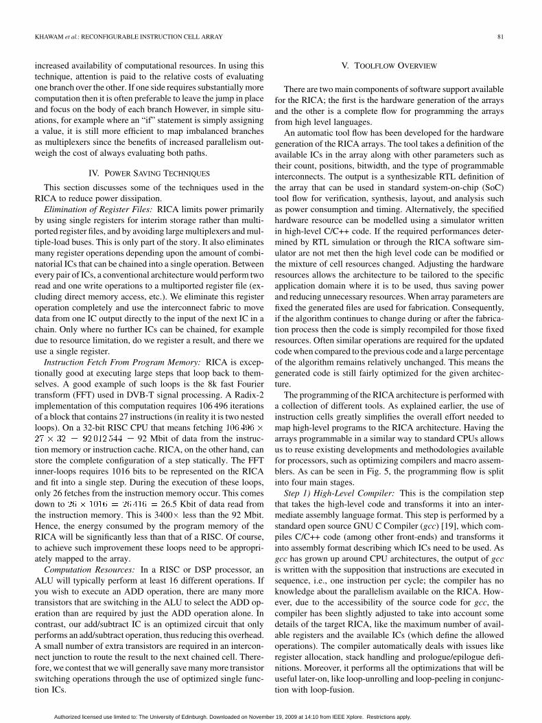
TABLE IVCOMPARISON OF DATAPATH AREA IN MILLIMETERS SQUARED ON 0.13-�m OF
VARIOUS CPUS EXCLUDING VARIATIONS IN PROGRAM MEMORY
Fig. 7. Normalized execution time graph of the benchmarks on RICA and otherarchitectures.
Fig. 8. Normalized energy consumption graph of the benchmarks on RICA andother architectures.
same for all processors, and hence it is not included in the com-parison. The Dhrystone benchmark, which today has become anoutdated measurement, is included here for reference. As shownin Table V, the fact that the Dhrystone takes more cycles to runon the highly pipelined TI DSPs than on the ARM7 shows howinappropriate a benchmark it is for modern processors.
B. Results
The results are listed in Tables IV and V and Figs. 7 and 8.From the tables, we can see that for all the benchmarks we
achieve better performance on the RICA than on the conven-tional OR32 and ARM7 CPUs; we get around 1–3.6 less en-ergy consumption while achieving around 5–8 higher max-imum throughput. Due to the increase in program memory size
and the increase in the datapath area, the power and throughputimprovements come at the cost of an area increase of around7 . A big part of the power reductions achieved over the fourDSP systems are savings gained by eliminating the register-filesand having distributed registers.
When compared to the low-power C55X DSP, RICAachieves a promising reduction in energy consumption between2 to 6 while achieving a throughput of up to 3 higher.RICA achieves similar timing performances to the VLIW forapplications containing significant datapath operations suchas the DCT, while faster operation is seen for Dhrystone. Forbenchmarks that have a lot of independent blocks and controlparts (i.e., small loops and comparisons) like minimum error,RICA is around 50% slower than the 600-MHz VLIW—this isexpected as the TI compiler can optimize such code by usingtechniques like predication in a better way than gcc. For theViterbi and IIR, RICA was around 20%–30% slower with thebottleneck being the memory access. However, for the case ofthe Viterbi, the gcc compiler was able to correctly identify theuse of multiplexers ICs which improved speeds and reducedbranching. It should also be noted that the RICA is built fromsynthesizable standard-cell libraries while the circuits in theVLIW have been manually laid out to achieve the 600-MHzoperating frequency. In terms of energy, around 6 less poweris consumed for DCT, Viterbi, and Dhrystone, since the RICAgoes less into states where ALUs are idle but consuming powerthan the VLIW. The power reductions for the minimum errorand IIR benchmarks were lower at around 17%. In terms ofarea, the datapaths of the RICA and VLIW are similar.
VII. CONCLUSION
In this paper, we presented a new coarse-grain reconfigurablecomputing architecture that offers comparable computationperformance to leading DSP processors with a significant re-duction in power consumption. The development of RICA wasprogressed bearing in mind the problem of taking a high-leveldescription of an algorithm and mapping it directly into the re-configurable fabric, as well as having an integrated control flowhandling to enable it to function independently to a standardprocessor, unlike some reconfigurable fabrics. This approachled to the adoption of an instruction-cell-based architecture,making RICA compatible with instruction representations ofprograms, and thus allowing seamless integration to existingwell established software design tool-flows. This is RICA’sdistinctive strength over other reconfigurable architectures thatlack a straightforward programming interface.
The architecture demonstrates good results regarding thefour important requirements for future systems: low-NRE costs,low-power consumption, high-flexibility, and straightforwarddesign-flow. Unlike conventional reprogrammable FPGAs, theRICA architecture is easily reprogrammed through high-levellanguages like conventional processors, which is done usingexisting compilers technologies such as the standard GNUCompiler. The RICA outperforms current low-power DSParchitectures such as the TI C55x by providing up to 3 higherthroughputs but with 2–6 less power consumption at a cost ofincreased program size. It should be noted that the full extent
Authorized licensed use limited to: The University of Edinburgh. Downloaded on November 19, 2009 at 14:10 from IEEE Xplore. Restrictions apply.

84 IEEE TRANSACTIONS ON VERY LARGE SCALE INTEGRATION (VLSI) SYSTEMS, VOL. 16, NO. 1, JANUARY 2008
TABLE VCOMPARING RICA WITH OTHER PROCESSOR, LOW-POWER DSP, AND VLIWS USING BENCHMARKS
of power savings depends on the amount of control operationsin the program.
When compared to current VLIW processors, RICA consid-erably reduces the number of required clock cycles in applica-tions containing numerous dependent instructions since it al-lows the execution of both dependent and independent instruc-tions in the same cycle, which overcomes the problem of statis-tical ILP-limit faced by VLIW. In terms of performance, RICAachieves similar timing to the VLIW for datapath applications,while being up to 50% slower in control intensive applications.This is due to the fact that the VLIW circuitry has been hand-crafted to achieve 600-MHz operating frequency. Nevertheless,RICA can achieve up to 6 less power than the VLIW.
The measured performance of the initial array are encour-aging, however, more changes can be done on the compilerlevel, such as making the scheduling occur inside gcc, to greatlyboost the performance.
REFERENCES
[1] G. Estrin, “Organization of computer systems—The fixed plus variablestructure computer,” in Proc. Western Joint Comput. Conf., 1960, pp.33–40.
[2] E. Mirsky and A. DeHon, “Matrix: A reconfigurable computing ar-chitecture with configurable instruction distribution and deployable re-sources,” in Proc. IEEE Symp. FPGAs Custom Comput. Mach., 1996,pp. 157–166.
[3] J. R. Hauser, “Augmenting a microprocessor with reconfigurable hard-ware,” M.S. thesis, Comput. Sci. Dept., Univ. California, Berkeley,2000.
[4] Elixent Ltd., Bristol, U.K., “D-Fabrix processing array, reconfigurablesignal processor,” 2005 [Online]. Available: www.elixent.com
[5] XPP, PACT, Munich, Germany, “OFDM decoder for wirelessLAN—Whitepaper,” May 2002 [Online]. Available: ww.pactcorp.com
[6] Philips, Avispa, Eindhoven, The Netherlands, “Reconfigurable com-puting,” 2005 [Online]. Available: www.siliconhive.com
[7] P. M. Heysters, G. J. M. Smit, and E. Molenkamp, “Montium—Bal-ancing between energy-efficiency, flexibility and performance,” Eng.Reconfig. Syst. Algorithms, pp. 235–241, 2003.
[8] M. Wan, H. Zhang, V. George, M. Benes, A. Abnous, V. Prabhu, and J.Rabaey, “Design methodology of a low energy reconfigurable single-chip dsp system,” J. VLSI Signal Process., vol. 28, pp. 53–63, 2000.
[9] H. Singh, M. Lee, G. Lu, F. Kurdahi, N. Bagherzadeh, and E. Filho,“MorphoSys: An integrated reconfigurable system for data-parallel andcomputation-intensive applications,” IEEE Trans. Comput., vol. 49, no.5, pp. 465–481, May 2000.
[10] S. Khawam, S. Baloch, A. Pai, I. Ahmed, N. Aydin, T. Arslan, andF. Westall, “Efficient implementations of mobile video computationson domain-specific reconfigurable arrays,” in Des. Autom. Test Eur.(DATE), 2004, pp. 1230–1235.
[11] B. Mei, S. Vernalde, D. Verkest, H. De Man, and R. Lauwereins,“ADRES: An architecture with tightly coupled VLIW processorand coarse-grained reconfigurable matrix,” in Proc. 3rd Int. Conf.Field-Program. Logic Appl., 2003, pp. 61–70.
[12] C. Ebeling, C. Fisher, G. Xing, M. Shen, and H. Lui, “Implementing anOFDM receiver on the rapid reconfigurable architecture,” IEEE Trans.Comput., vol. 53, no. 11, pp. 1436–1448, Nov. 2004.
[13] Stretch, Sunnyvale, CA, “Configurable processor,” 2007 [Online].Available: www.stretchinc.com
[14] R. Baines and D. Pulley, “A total cost approach to evaluating differentreconfigurable architectures for baseband processing in wireless re-ceivers,” IEEE Commun. Mag., vol. 41, no. 1, pp. 105–113, Jan. 2003.
[15] Ambric, OR, “Programmable multicore,” 2007 [Online]. Available:www.ambric.com
[16] S. Agarwala et al., “A 600-MHz VLIW DSP,” IEEE J. Solid-State Cir-cuits, vol. 37, no. 11, pp. 1532–1544, Nov. 2002.
[17] Opencores, Dobrova, Slovenia, “OpenRISC,” (2005). [Online]. Avail-able: http://www.opencores.org/projects.cgi/web/or1k
[18] J. Rose and S. Brown, “Flexibility of interconnection structures forfield-programmable gate arrays,” IEEE J. Solid-State Circuits, vol. 26,no. 3, pp. 277–282, Mar. 1990.
[19] GNU, Boston, MA, “GNU C compiler,” 2005 [Online]. Available:http://gcc.gnu.org/
Authorized licensed use limited to: The University of Edinburgh. Downloaded on November 19, 2009 at 14:10 from IEEE Xplore. Restrictions apply.

KHAWAM et al.: RECONFIGURABLE INSTRUCTION CELL ARRAY 85
[20] V. Betz and J. Rose, “VPR: A new packing, placement and routing toolfor FPGA research,” in Proc. 7th Int. Workshop Field-Program. Logic,1997, pp. 213–222.
[21] ARM Ltd., Cambridge, U.K., “ARM7 thumb family datasheet,” ARMDOI 0035-3/02.02, 2002.
[22] G. Martinez, “TI TMS320VC5501/02 power consumption summary,”Appl. Rep. SPRAA48, 2004.
[23] Y. Yi, I. Nousias, M. Milward, S. Khawam, T. Arslan, and I. Lindsay,“System-level scheduling on instruction cell based reconfigurablesystems,” in Proc. Des. Autom. Test Eur. Conf. (DATE), 2006, pp.381–386.
[24] Texas Instruments Incorporated, Dallas, TX, “TMS320C5000 CPU andinstruction set reference guide,” 2000.
[25] G. Martinez, “TMS320VC5501/02 power consumption summary,”Appl. Rep. TI SPRAA48, 2004.
[26] D. Wentzlaff, “Architectural implications of bit-level computation incommunication applications,” M.Sc. thesis, Dept. Elect. Eng. Comput.Sci., Massachusetts Inst. Technol., Boston, 2002.
[27] N. Aslam, M. Milward, I. Nousias, T. Arslan, and A. Erdogan, “Codecompression and decompression for instruction cell based reconfig-urable systems,” presented at the IEEE Int. Parallel Distrib. Process.Symp., Reconfigurable Arch. Workshop, Long Beach, CA, 2007.
[28] N. Aslam, M. Milward, I. Nousias, T. Arslan, and A. Erdogan, “Codecompressor and decompressor for ultra large instruction width coarse-grain reconfigurable systems,” in Proc. IEEE Symp. Field-Program.Custom Comput. Mach., 2007, pp. 297–298.
Sami Khawam received the B.Eng. degree in elec-trical and electronics engineering and the Ph.D. de-gree in system level integration from the Universityof Edinburgh, Edinburgh, U.K., in 2001 and 2006, re-spectively.
Presently, he is a Senior Hardware Engineerwith SpiralGateway, Edinburgh, U.K. His researchinterests include low-power VLSI hardware, recon-figurable hardware architectures, and embeddedreconfigurable hardware.
Ioannis Nousias received the B.Sc. degree in elec-trical and electronic engineering from the Cretan Uni-versity, Chania, Greece, in 2001, and the M.Sc. de-gree in system level integration from the Universityof Edinburgh, Edinburgh, U.K., in 2003, where he iscurrently pursuing the Ph.D. degree in reconfigurablecomputing.
In June 2007, he became a Senior Engineer withSpiral Gateway LTD, Edinburgh, U.K., where hecontinues his work in reconfigurable computingtechnologies. In 2001, he was a Senior Hardware and
Software Engineer with Protogenea Inc., Athens, Greece, where he developeda GPS- and GSM-based tracking and monitoring system for industrial andsmall business applications, such as terrestrial map alignment and remotemonitoring of containers with sensitive shipments. His research interestsinclude reconfigurable computing, bioinspired technologies, artificial intelli-gence, interconnection technologies, network on chip, and micro-processorarchitectures.”
Mark John Milward received the B.Eng. degree inelectronic and electrical engineering and the Ph.D.degree in the area of parallel lossless compressionfrom Loughborough University, Leicestershire, U.K.,in 2000 and 2004, respectively.
Currently, he is a Senior Engineer with SpiralGateway Ltd., Edinburgh, U.K., where he is contin-uing his work on reconfigurable systems. He was aResearch Associate with the System Level Integra-tion Group, University of Edinburgh, Edinburgh,U.K. His research interests include reconfigurable
architectures, parallel hardware architectures, and lossless compression.
Ying Yi received the B.Sc. degree in computer andapplication from Harbin Engineering University,Harbin, China, and the Ph.D. degree from theQueen’s University, Belfast, U.K., in 1996 and 2003,respectively.
Currently, she is a Research Fellow with the Schoolof Engineering and Electronics, University of Edin-burgh, Edinburgh, U.K. She was a Software Engi-neer with the WuHan Institute of Mathematical En-gineering, China, where she researched, developed,and maintained intranet and management informa-
tion systems. From 1997 to 2000, she was with the China Ship Research andDevelopment Academy (CSRDA), Beijing, China, where she was involved inresearch, development, and management of computer correlative problems. Herresearch interests include low-power reconfigurable SoC systems, compiler op-timization techniques for reconfigurable architecture, architectural level syn-thesis optimization, and multiprocessor SoC.
Mark Muir received the M.Eng. degree (first class)in electrical and mechanical engineering and thePh.D. degree from the University of Edinburgh,Edinburgh, U.K., in 2004, where he developedsoftware tools for the RICA project.
He is currently writing up, and is an employee ofSpiral Gateway, Edinburgh, U.K., which licenses thistechnology. His research includes a broad range ofinterests, with particular emphasis on software devel-opment and algorithms.
Tughrul Arslan holds the Chair of Integrated Elec-tronic Systems with the School of Engineering andElectronics, University of Edinburgh, Edinburgh,U.K., and is also a cofounder and the Chief TechnicalOfficer of SpiralGateway Ltd., Edinburgh, U.K. Heis a member of the Integrated Micro and NanoSystems (IMNS) Institute and leads the SystemLevel Integration Group (SLIg) in the University.his research interests include low-power design,DSP hardware design, system-on-chip (SOC) ar-chitectures, evolvable hardware, multiobjective
optimization, and the use of genetic algorithms in hardware design issues.Prof. Arslan is an Associate Editor for the IEEE TRANSACTIONS ON CIRCUITS
AND SYSTEMS—I: REGULAR PAPERS, a member of the IEEE CAS Committeeon VLSI Systems and Applications, and sits on the editorial board of IEE Pro-ceedings on Computers and Digital Techniques and the technical committeesof a number of international conferences. This year he is the general Chair ofthe NASA/ESA Conference on Adaptive Hardware and Systems, and Co-Chairof ECSIS Bio-inspired, Learning, and Intelligent Systems for Security Sympo-sium (BLISS). He is a principal investigator on a number of projects funded byEPSRC, DTI, and Scottish Enterprise together with a number of industrial andacademic partners.
Authorized licensed use limited to: The University of Edinburgh. Downloaded on November 19, 2009 at 14:10 from IEEE Xplore. Restrictions apply.