Positive Bias Instability and Recovery in InGaAs Channel nMOSFETs
8
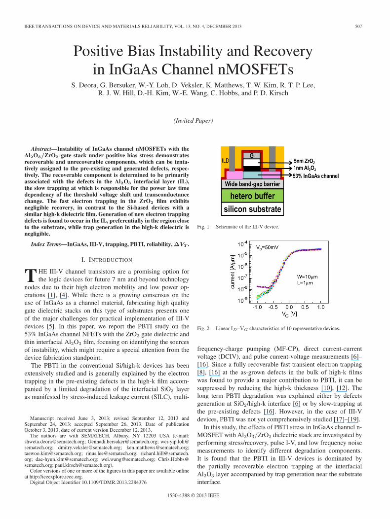
IEEE TRANSACTIONS ON DEVICE AND MATERIALS RELIABILITY, VOL. 13, NO. 4, DECEMBER 2013 507 Positive Bias Instability and Recovery in InGaAs Channel nMOSFETs S. Deora, G. Bersuker, W.-Y. Loh, D. Veksler, K. Matthews, T. W. Kim, R. T. P. Lee, R. J. W. Hill, D.-H. Kim, W.-E. Wang, C. Hobbs, and P. D. Kirsch (Invited Paper) Abstract—Instability of InGaAs channel nMOSFETs with the Al 2 O 3 /ZrO 2 gate stack under positive bias stress demonstrates recoverable and unrecoverable components, which can be tenta- tively assigned to the pre-existing and generated defects, respec- tively. The recoverable component is determined to be primarily associated with the defects in the Al 2 O 3 interfacial layer (IL), the slow trapping at which is responsible for the power law time dependency of the threshold voltage shift and transconductance change. The fast electron trapping in the ZrO 2 film exhibits negligible recovery, in contrast to the Si-based devices with a similar high-k dielectric film. Generation of new electron trapping defects is found to occur in the IL, preferentially in the region close to the substrate, while trap generation in the high-k dielectric is negligible. Index Terms—InGaAs, III-V, trapping, PBTI, reliability, ΔV T . I. I NTRODUCTION T HE III-V channel transistors are a promising option for the logic devices for future 7 nm and beyond technology nodes due to their high electron mobility and low power op- erations [1], [4]. While there is a growing consensus on the use of InGaAs as a channel material, fabricating high quality gate dielectric stacks on this type of substrates presents one of the major challenges for practical implementation of III-V devices [5]. In this paper, we report the PBTI study on the 53% InGaAs channel NFETs with the ZrO 2 gate dielectric and thin interfacial Al 2 O 3 film, focusing on identifying the sources of instability, which might require a special attention from the device fabrication standpoint. The PBTI in the conventional Si/high-k devices has been extensively studied and is generally explained by the electron trapping in the pre-existing defects in the high-k film accom- panied by a limited degradation of the interfacial SiO 2 layer as manifested by stress-induced leakage current (SILC), multi- Manuscript received June 3, 2013; revised September 12, 2013 and September 24, 2013; accepted September 26, 2013. Date of publication October 3, 2013; date of current version December 12, 2013. The authors are with SEMATECH, Albany, NY 12203 USA (e-mail: [email protected]; [email protected]; wei-yip.loh@ sematech.org; [email protected]; [email protected]; [email protected]; [email protected]; richard.hill@sematech. org; [email protected]; [email protected]; Chris.Hobbs@ sematech.org; [email protected]). Color versions of one or more of the figures in this paper are available online at http://ieeexplore.ieee.org. Digital Object Identifier 10.1109/TDMR.2013.2284376 Fig. 1. Schematic of the III-V device. Fig. 2. Linear I D –V G characteristics of 10 representative devices. frequency-charge pumping (MF-CP), direct current-current voltage (DCIV), and pulse current-voltage measurements [6]– [16]. Since a fully recoverable fast transient electron trapping [8], [16] at the as-grown defects in the bulk of high-k films was found to provide a major contribution to PBTI, it can be suppressed by reducing the high-k thickness [10], [12]. The long term PBTI degradation was explained either by defects generation at SiO 2 /high-k interface [6] or by slow-trapping at the pre-existing defects [16]. However, in the case of III-V devices, PBTI was not yet comprehensively studied [17]–[19]. In this study, the effects of PBTI stress in InGaAs channel n- MOSFET with Al 2 O 3 /ZrO 2 dielectric stack are investigated by performing stress/recovery, pulse I-V, and low frequency noise measurements to identify different degradation components. It is found that the PBTI in III-V devices is dominated by the partially recoverable electron trapping at the interfacial Al 2 O 3 layer accompanied by trap generation near the substrate interface. 1530-4388 © 2013 IEEE
-
Upload
independent -
Category
Documents
-
view
3 -
download
0
Transcript of Positive Bias Instability and Recovery in InGaAs Channel nMOSFETs
IEEE TRANSACTIONS ON DEVICE AND MATERIALS RELIABILITY, VOL. 13, NO. 4, DECEMBER 2013 507
Positive Bias Instability and Recoveryin InGaAs Channel nMOSFETs
S. Deora, G. Bersuker, W.-Y. Loh, D. Veksler, K. Matthews, T. W. Kim, R. T. P. Lee,R. J. W. Hill, D.-H. Kim, W.-E. Wang, C. Hobbs, and P. D. Kirsch
(Invited Paper)
Abstract—Instability of InGaAs channel nMOSFETs with theAl2O3/ZrO2 gate stack under positive bias stress demonstratesrecoverable and unrecoverable components, which can be tenta-tively assigned to the pre-existing and generated defects, respec-tively. The recoverable component is determined to be primarilyassociated with the defects in the Al2O3 interfacial layer (IL),the slow trapping at which is responsible for the power law timedependency of the threshold voltage shift and transconductancechange. The fast electron trapping in the ZrO2 film exhibitsnegligible recovery, in contrast to the Si-based devices with asimilar high-k dielectric film. Generation of new electron trappingdefects is found to occur in the IL, preferentially in the region closeto the substrate, while trap generation in the high-k dielectric isnegligible.
Index Terms—InGaAs, III-V, trapping, PBTI, reliability, ΔVT .
I. INTRODUCTION
THE III-V channel transistors are a promising option forthe logic devices for future 7 nm and beyond technology
nodes due to their high electron mobility and low power op-erations [1], [4]. While there is a growing consensus on theuse of InGaAs as a channel material, fabricating high qualitygate dielectric stacks on this type of substrates presents oneof the major challenges for practical implementation of III-Vdevices [5]. In this paper, we report the PBTI study on the53% InGaAs channel NFETs with the ZrO2 gate dielectric andthin interfacial Al2O3 film, focusing on identifying the sourcesof instability, which might require a special attention from thedevice fabrication standpoint.
The PBTI in the conventional Si/high-k devices has beenextensively studied and is generally explained by the electrontrapping in the pre-existing defects in the high-k film accom-panied by a limited degradation of the interfacial SiO2 layeras manifested by stress-induced leakage current (SILC), multi-
Manuscript received June 3, 2013; revised September 12, 2013 andSeptember 24, 2013; accepted September 26, 2013. Date of publicationOctober 3, 2013; date of current version December 12, 2013.
The authors are with SEMATECH, Albany, NY 12203 USA (e-mail:[email protected]; [email protected]; [email protected]; [email protected]; [email protected];[email protected]; [email protected]; [email protected]; [email protected]; [email protected]; [email protected]; [email protected]).
Color versions of one or more of the figures in this paper are available onlineat http://ieeexplore.ieee.org.
Digital Object Identifier 10.1109/TDMR.2013.2284376
Fig. 1. Schematic of the III-V device.
Fig. 2. Linear ID–VG characteristics of 10 representative devices.
frequency-charge pumping (MF-CP), direct current-currentvoltage (DCIV), and pulse current-voltage measurements [6]–[16]. Since a fully recoverable fast transient electron trapping[8], [16] at the as-grown defects in the bulk of high-k filmswas found to provide a major contribution to PBTI, it can besuppressed by reducing the high-k thickness [10], [12]. Thelong term PBTI degradation was explained either by defectsgeneration at SiO2/high-k interface [6] or by slow-trapping atthe pre-existing defects [16]. However, in the case of III-Vdevices, PBTI was not yet comprehensively studied [17]–[19].
In this study, the effects of PBTI stress in InGaAs channel n-MOSFET with Al2O3/ZrO2 dielectric stack are investigated byperforming stress/recovery, pulse I-V, and low frequency noisemeasurements to identify different degradation components.It is found that the PBTI in III-V devices is dominated bythe partially recoverable electron trapping at the interfacialAl2O3 layer accompanied by trap generation near the substrateinterface.
1530-4388 © 2013 IEEE
508 IEEE TRANSACTIONS ON DEVICE AND MATERIALS RELIABILITY, VOL. 13, NO. 4, DECEMBER 2013
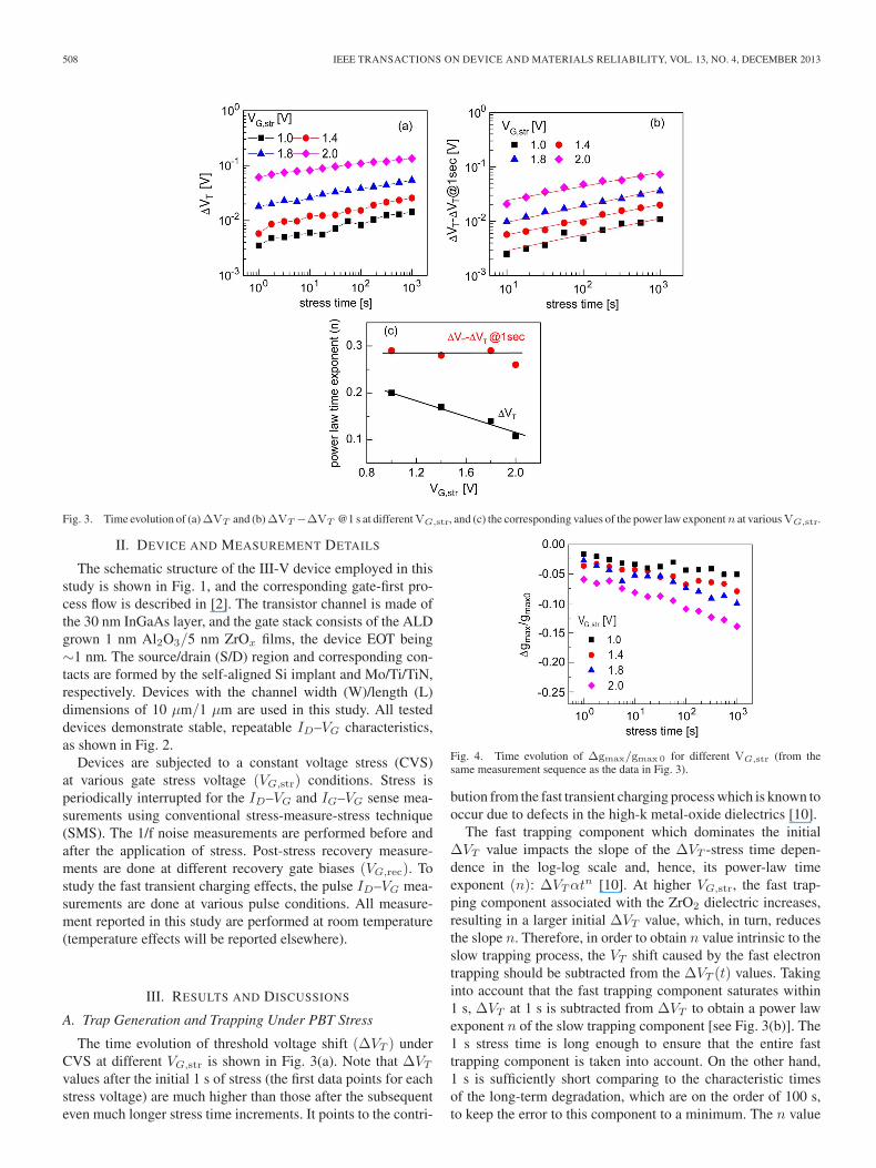
Fig. 3. Time evolution of (a)ΔVT and (b)ΔVT −ΔVT @1 s at differentVG,str, and (c) the corresponding values of the power law exponentn at variousVG,str.
II. DEVICE AND MEASUREMENT DETAILS
The schematic structure of the III-V device employed in thisstudy is shown in Fig. 1, and the corresponding gate-first pro-cess flow is described in [2]. The transistor channel is made ofthe 30 nm InGaAs layer, and the gate stack consists of the ALDgrown 1 nm Al2O3/5 nm ZrOx films, the device EOT being∼1 nm. The source/drain (S/D) region and corresponding con-tacts are formed by the self-aligned Si implant and Mo/Ti/TiN,respectively. Devices with the channel width (W)/length (L)dimensions of 10 μm/1 μm are used in this study. All testeddevices demonstrate stable, repeatable ID–VG characteristics,as shown in Fig. 2.
Devices are subjected to a constant voltage stress (CVS)at various gate stress voltage (VG,str) conditions. Stress isperiodically interrupted for the ID–VG and IG–VG sense mea-surements using conventional stress-measure-stress technique(SMS). The 1/f noise measurements are performed before andafter the application of stress. Post-stress recovery measure-ments are done at different recovery gate biases (VG,rec). Tostudy the fast transient charging effects, the pulse ID–VG mea-surements are done at various pulse conditions. All measure-ment reported in this study are performed at room temperature(temperature effects will be reported elsewhere).
III. RESULTS AND DISCUSSIONS
A. Trap Generation and Trapping Under PBT Stress
The time evolution of threshold voltage shift (ΔVT ) underCVS at different VG,str is shown in Fig. 3(a). Note that ΔVT
values after the initial 1 s of stress (the first data points for eachstress voltage) are much higher than those after the subsequenteven much longer stress time increments. It points to the contri-
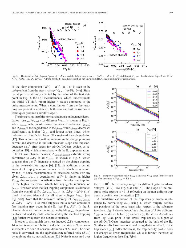
Fig. 4. Time evolution of Δgmax/gmax 0 for different VG,str (from thesame measurement sequence as the data in Fig. 3).
bution from the fast transient charging process which is known tooccur due to defects in the high-k metal-oxide dielectrics [10].
The fast trapping component which dominates the initialΔVT value impacts the slope of the ΔVT -stress time depen-dence in the log-log scale and, hence, its power-law timeexponent (n): ΔVTαt
n [10]. At higher VG,str, the fast trap-ping component associated with the ZrO2 dielectric increases,resulting in a larger initial ΔVT value, which, in turn, reducesthe slope n. Therefore, in order to obtain n value intrinsic to theslow trapping process, the VT shift caused by the fast electrontrapping should be subtracted from the ΔVT (t) values. Takinginto account that the fast trapping component saturates within1 s, ΔVT at 1 s is subtracted from ΔVT to obtain a power lawexponent n of the slow trapping component [see Fig. 3(b)]. The1 s stress time is long enough to ensure that the entire fasttrapping component is taken into account. On the other hand,1 s is sufficiently short comparing to the characteristic timesof the long-term degradation, which are on the order of 100 s,to keep the error to this component to a minimum. The n value
DEORA et al.: POSITIVE BIAS INSTABILITY AND RECOVERY IN InGaAs CHANNEL nMOSFET 509
Fig. 5. The trends of (a) (Δgmax/gmax 0)−ΔVT and (b) (Δgmax/gmax 0)− (ΔVT −ΔVT (1 s)) at different VG,str (the data from Figs. 3 and 4) forAl2O3/ZrO2/InGaAs devices. A trend for the Si-based devices (Si/1 nm SiOx/3 nm HfO2 stack) is shown for comparison.
of the slow component (ΔVT −ΔVT at 1 s) is seen to beindependent from the stress voltage VG,str [see Fig. 3(c)]. Sincethe slope n is strongly affected by the value of the first datapoint in Fig. 3, the DC measurements, which underestimatethe initial VT shift, report higher n values compared to thepulse measurements. When a contribution from the fast trap-ping component is subtracted, both slow and fast measurementtechniques produce a similar slope n.
The time evolution of the normalized transconductance degra-dation (Δgmax/gmax0) for different VG,str is shown in Fig. 4,where gmax0 is the pre-stress maximum transconductance (gmax)and Δgmax is the degradation in the gmax value. gmax decreasessignificantly at higher VG,str and longer stress times, whichindicates an interfacial layer (IL) region-driven degradation[12]. This is consistent with an increase in the charge pumpingcurrent and decrease in the sub-threshold slope and transcon-ductance (gm) after stress for Al2O3/InGaAs device, as re-ported in [19], which is associated with the IL trap generation.
In InGaAs channel devices, Δgmax/gmax0 exhibits strongcorrelation to ΔVT at all VG,str, as shown in Fig. 5, whichsuggests that the VT increase is caused by the charge trappingin the near-substrate region [6], [12]. In addition, a certainamount of trap generation occurs in IL which is observedby the 1/f noise measurements, as discussed below. For anygiven Δgmax/gmax0 degradation, ΔVT is higher at higherVG,str due to greater contribution from the electron trappingin the high-k dielectric, which has negligible influence ongmax. However, once the fast trapping component is subtractedfrom the overall ΔVT , Δgmax/gmax0 vs. ΔVT −ΔVT (1 s)trend is almost identical for all stress voltages VG,str [seeFig. 5(b)]. Note that the non-zero intercept of Δgmax/gmax0
vs. ΔVT −ΔVT (1 s) trend suggests that a certain amount offast trapping may occur in the IL [see Fig. 5(b)]. In the Sichannel devices, on the contrary, negligible gmax degradationis observed, and VT shift is dominated by the electron trapping[12] further away from the substrate interface.
In order to distinguish the stress-induced ΔVT components,1/f noise is measured before and after the stress. Noise mea-surements are done at constant drain bias of 50 mV. The drainnoise is converted into the equivalent gate referred noise (SVG)by applying the gm normalization [22]. Noise is measured over
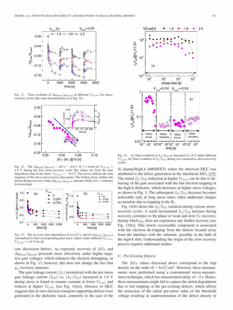
Fig. 6. The power spectral density SVG at different VGT taken (a) before and(b) after the stress at VG,str = 1.8 V.
the 10−105 Hz frequency range for different gate overdrivevoltages (VGT) [see Fig. 6(a) and (b)]. The slope of the pre-stress noise spectra is ∼1.18 reflecting on the non-uniform trapdensity profile near the interface [22].
A qualitative estimation of the trap density profile is ob-tained by normalizing SVG using f , which roughly definesthe positions of the noise traps with respect to the substrateinterface. Fig. 7 shows SVGxf as a function of f for differentVGT in the device before (a) and after (b) the stress. As followsfrom Fig. 7(a), prior to the stress, trap density is higher atthe Al2O3/InGaAs interface compared to the bulk of the IL.Similar results have been obtained using distributed bulk oxidetrap model [21]. After the stress, the trap density profile doesnot change at lower frequencies while it further increases athigher frequencies [see Fig. 7(b)].
510 IEEE TRANSACTIONS ON DEVICE AND MATERIALS RELIABILITY, VOL. 13, NO. 4, DECEMBER 2013
Fig. 7. The normalized power spectral density SVGxf as a function of fre-quency measured at various VGT before (a) and after (b) the VG,str = 1.8 Vstress (from data in Fig. 6).
Fig. 8. ΔNtotal as a function of VG,str extracted from the noise spectra inFig. 7 at high (near- substrate interface region) and low (through the entire ILthickness) frequencies.
Fig. 8 shows the extracted total generated trap density(ΔNtotal) as a function of VG,str, as obtained from the 1/f noisespectra at different frequencies [22]. ΔNtotal is by approxi-mately an order of magnitude higher at high frequency (105 Hz)compared to that of a lower frequency (10 Hz), indicatingthat the trap generation occurs more efficiently closer to thesubstrate interface. There can be some variation in the exactlocation of the generated defects due to difference in the gatestack and the measurement technique being used [19].
B. Trap Recovery
The time evolution of ΔVT for two consecutive stress-recovery cycles measured at different VG,str shows that ΔVT
Fig. 9. Time evolution of ΔVT at different VG,str during the stress-recovery-stress cycles. Recovery is done at −0.5 V for all VG,str values.
Fig. 10. The trend of ΔVT after recovery vs. ΔVT after end of stress in twoconsecutive stress-recovery cycles from different VG,str. Two data points foreach stress voltage correspond to two stress-recovery cycles.
partially recovers after stress [see Fig. 9]. VG,rec = −0.5 V isapplied after end of every stress. Since the device thresholdvoltage VT ∼ −0.2 V, VG,rec < VT is chosen in order to de-trap defects throughout the band-gap.
A trend of ΔVT at the end of recovery vs ΔVT at the end ofstress for two subsequent stress-recovery cycles for each stressvoltage is plotted in Fig. 10; ΔVT recovers by approximately35% for all VG,str at a given recovery bias and time. The datashow that the recovery is independent from the stress voltageand is strictly proportional to the amount of the trapped charge.
The time evolution of Δgmax/gmax0 during the stress-recovery cycles is presented in Fig. 11. Similar to ΔVT , Δgmax
also recovers partially.An example of correlation between Δgmax/gmax0 and a slow
ΔVT component [after subtracting the fast transient chargingcontribution as in Fig. 5(b)] during the stress-recovery cycle fora given VG,str is presented in Fig. 12; the time dependence ofΔVT and Δgmax/gmax0 is shown in the inset. For a given VG,str
magnitude, the ΔVT and Δgmax/gmax0 stress and recoverytrends are similar, suggesting that at least a significant portionof the slow ΔVT component can be attributed to the electrontrapping/de-trapping at the IL defects. The Δgmax/gmax0 re-covery saturates at some point in time, while the ΔVT recoveryslowly proceeds (see also Fig. 13), which could be due to thede-trapping from the defects located at a sufficient distancefrom the substrate interface, either in IL or in high-k film
DEORA et al.: POSITIVE BIAS INSTABILITY AND RECOVERY IN InGaAs CHANNEL nMOSFET 511
Fig. 11. Time evolution of Δgmax/gmax 0 at different VG,str for stress-recovery cycles (the same measurements as in Fig. 10).
Fig. 12. The Δgmax/gmax 0 −ΔVT −ΔVT @ 1 s trend for VG,str =1.8 V during the first stress-recovery cycle (the values are from the timedependency data in the inset). VG,rec = −0.5 V. The arrows indicate the timesequence of the stress and recovery data points. The broken arrow outlines theperiod during recovery when Δgmax/gmax 0 saturates while ΔVT continuesits recovering.
Fig. 13. The recovery time dependency of (a) ΔVT and (b) Δgmax/gmax 0
(normalized to their corresponding post-stress values) under different VG,rec.VG,str = 1.6 V for all.
(see discussion below). As expected, recovery of ΔVT andΔgmax/gmax0 proceeds more effectively under higher nega-tive gate voltages, which enhances the electron detrapping, asshown in Fig. 13, however, this does not change the fact thatgm recovery saturates.
The gate leakage current (IG) normalized with the pre-stressgate leakage current (IG0) i.e. (IG/IG0) measured at 1.0 Vduring stress is found to remain constant at lower VG,str andreduces at higher VG,str [see Fig. 14(a)]. Absence of SILCsuggests that no new electron transport-supporting defects weregenerated in the dielectric stack, contrarily to the case of the
Fig. 14. (a) Time evolution of IG/IG0 as measured at 1.0 V under differentVG,str (b) Time evolution of IG/IG0 during two consecutive stress-recoverycycles.
Si channel/high-k nMOSFETs where the observed SILC wasattributed to the defect generation in the interfacial SiOx [15].The initial IG/IG0 reduction at higher VG,str can be due to de-biasing of the gate associated with the fast electron trapping inthe high-k dielectric, which increases at higher stress voltages,as shown in Fig. 3. The subsequent IG/IG0 decrease becomesnoticeable only at long stress times when additional chargesaccumulate due to trapping in the IL.
Fig. 14(b) shows the IG/IG0 variation during various stress-recovery cycles. A small incremental IG/IG0 increase duringrecovery correlates to the phase of weak and slow VT recovery,during which gm does not experience any further recovery [seeFig. 13(b)]. This slowly recoverable component is associatedwith the electron de-trapping from the defects located awayfrom the interface with the substrate, possibly in the bulk ofthe high-k film. Understanding the origin of the slow recoveryprocess requires additional studies.
C. Pre-Existing Defects
The ΔVT values discussed above correspond to the trapdensity on the order of ∼1e12/cm2. However, these measure-ments were performed using a conventional stress-measure-stress technique, which has measurement delay of ∼2 s. Hence,these measurements might fail to capture the initial degradationdue to fast trapping at the pre-existing defects, which affectsthe extraction of the initial pre-stress value of the thresholdvoltage resulting in underestimation of the defect density in
512 IEEE TRANSACTIONS ON DEVICE AND MATERIALS RELIABILITY, VOL. 13, NO. 4, DECEMBER 2013
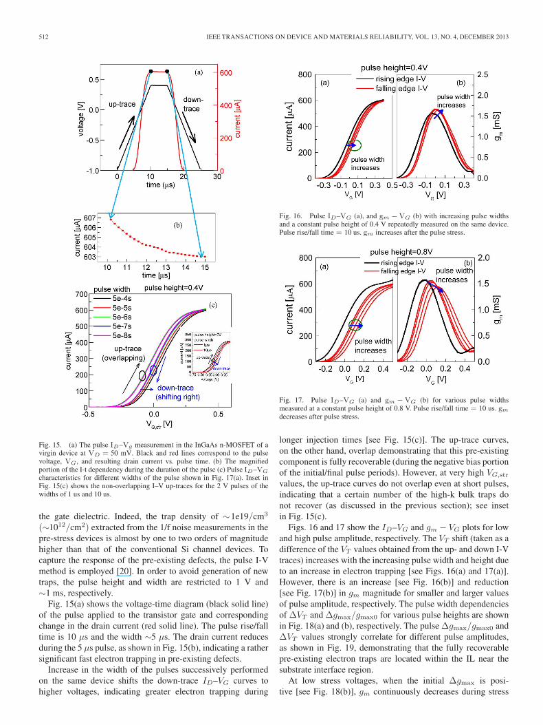
Fig. 15. (a) The pulse ID–Vg measurement in the InGaAs n-MOSFET of avirgin device at VD = 50 mV. Black and red lines correspond to the pulsevoltage, VG, and resulting drain current vs. pulse time. (b) The magnifiedportion of the I-t dependency during the duration of the pulse (c) Pulse ID–VG
characteristics for different widths of the pulse shown in Fig. 17(a). Inset inFig. 15(c) shows the non-overlapping I–V up-traces for the 2 V pulses of thewidths of 1 us and 10 us.
the gate dielectric. Indeed, the trap density of ∼1e19/cm3
(∼1012/cm2) extracted from the 1/f noise measurements in thepre-stress devices is almost by one to two orders of magnitudehigher than that of the conventional Si channel devices. Tocapture the response of the pre-existing defects, the pulse I-Vmethod is employed [20]. In order to avoid generation of newtraps, the pulse height and width are restricted to 1 V and∼1 ms, respectively.
Fig. 15(a) shows the voltage-time diagram (black solid line)of the pulse applied to the transistor gate and correspondingchange in the drain current (red solid line). The pulse rise/falltime is 10 μs and the width ∼5 μs. The drain current reducesduring the 5 μs pulse, as shown in Fig. 15(b), indicating a rathersignificant fast electron trapping in pre-existing defects.
Increase in the width of the pulses successively performedon the same device shifts the down-trace ID–VG curves tohigher voltages, indicating greater electron trapping during
Fig. 16. Pulse ID–VG (a), and gm −VG (b) with increasing pulse widthsand a constant pulse height of 0.4 V repeatedly measured on the same device.Pulse rise/fall time = 10 us. gm increases after the pulse stress.
Fig. 17. Pulse ID–VG (a) and gm −VG (b) for various pulse widthsmeasured at a constant pulse height of 0.8 V. Pulse rise/fall time = 10 us. gmdecreases after pulse stress.
longer injection times [see Fig. 15(c)]. The up-trace curves,on the other hand, overlap demonstrating that this pre-existingcomponent is fully recoverable (during the negative bias portionof the initial/final pulse periods). However, at very high VG,str
values, the up-trace curves do not overlap even at short pulses,indicating that a certain number of the high-k bulk traps donot recover (as discussed in the previous section); see insetin Fig. 15(c).
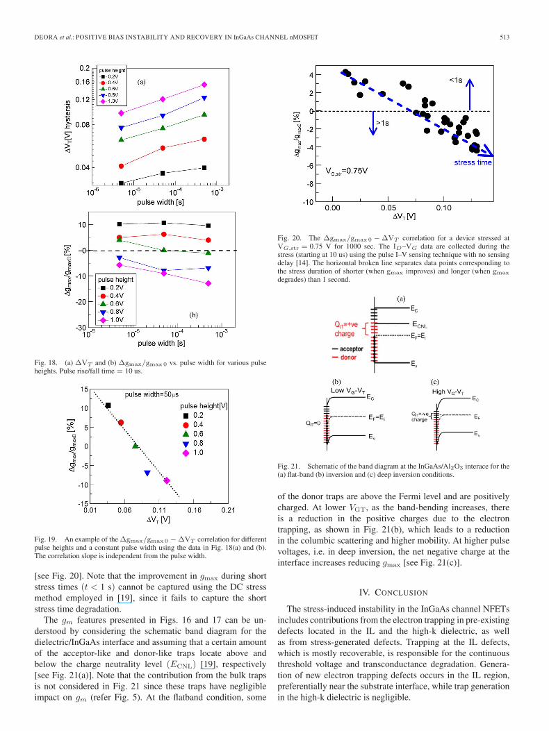
Figs. 16 and 17 show the ID–VG and gm − VG plots for lowand high pulse amplitude, respectively. The VT shift (taken as adifference of the VT values obtained from the up- and down I-Vtraces) increases with the increasing pulse width and height dueto an increase in electron trapping [see Figs. 16(a) and 17(a)].However, there is an increase [see Fig. 16(b)] and reduction[see Fig. 17(b)] in gm magnitude for smaller and larger valuesof pulse amplitude, respectively. The pulse width dependenciesof ΔVT and Δgmax/gmax0 for various pulse heights are shownin Fig. 18(a) and (b), respectively. The pulse Δgmax/gmax0 andΔVT values strongly correlate for different pulse amplitudes,as shown in Fig. 19, demonstrating that the fully recoverablepre-existing electron traps are located within the IL near thesubstrate interface region.
At low stress voltages, when the initial Δgmax is posi-tive [see Fig. 18(b)], gm continuously decreases during stress
DEORA et al.: POSITIVE BIAS INSTABILITY AND RECOVERY IN InGaAs CHANNEL nMOSFET 513
Fig. 18. (a) ΔVT and (b) Δgmax/gmax 0 vs. pulse width for various pulseheights. Pulse rise/fall time = 10 us.
Fig. 19. An example of the Δgmax/gmax 0 −ΔVT correlation for differentpulse heights and a constant pulse width using the data in Fig. 18(a) and (b).The correlation slope is independent from the pulse width.
[see Fig. 20]. Note that the improvement in gmax during shortstress times (t < 1 s) cannot be captured using the DC stressmethod employed in [19], since it fails to capture the shortstress time degradation.
The gm features presented in Figs. 16 and 17 can be un-derstood by considering the schematic band diagram for thedielectric/InGaAs interface and assuming that a certain amountof the acceptor-like and donor-like traps locate above andbelow the charge neutrality level (ECNL) [19], respectively[see Fig. 21(a)]. Note that the contribution from the bulk trapsis not considered in Fig. 21 since these traps have negligibleimpact on gm (refer Fig. 5). At the flatband condition, some
Fig. 20. The Δgmax/gmax 0 −ΔVT correlation for a device stressed atVG,str = 0.75 V for 1000 sec. The ID–VG data are collected during thestress (starting at 10 us) using the pulse I–V sensing technique with no sensingdelay [14]. The horizontal broken line separates data points corresponding tothe stress duration of shorter (when gmax improves) and longer (when gmax
degrades) than 1 second.
Fig. 21. Schematic of the band diagram at the InGaAs/Al2O3 interace for the(a) flat-band (b) inversion and (c) deep inversion conditions.
of the donor traps are above the Fermi level and are positivelycharged. At lower VGT, as the band-bending increases, thereis a reduction in the positive charges due to the electrontrapping, as shown in Fig. 21(b), which leads to a reductionin the columbic scattering and higher mobility. At higher pulsevoltages, i.e. in deep inversion, the net negative charge at theinterface increases reducing gmax [see Fig. 21(c)].
IV. CONCLUSION
The stress-induced instability in the InGaAs channel NFETsincludes contributions from the electron trapping in pre-existingdefects located in the IL and the high-k dielectric, as wellas from stress-generated defects. Trapping at the IL defects,which is mostly recoverable, is responsible for the continuousthreshold voltage and transconductance degradation. Genera-tion of new electron trapping defects occurs in the IL region,preferentially near the substrate interface, while trap generationin the high-k dielectric is negligible.
514 IEEE TRANSACTIONS ON DEVICE AND MATERIALS RELIABILITY, VOL. 13, NO. 4, DECEMBER 2013
REFERENCES
[1] M. Radosavljevic, G. Dewey, J. M. Fastenau, J. Kavalieros, R. Kotlyar,B. Chu-Kung, W. K. Liu, D. Lubyshev, M. Metz, K. Millard, N. Mukherjee,L. Pan, R. Pillarisetty, W. Rachmady, U. Shah, and R. Chau, “Non-planar,multi-gate InGaAs quantum well field effect transistors with high-k gatedielectric and ultra-scaled gate-to-drain/gate-to-source separation for lowpower logic applications,” in Proc. IEDM, 2010, p. 6.1.1.
[2] R. J. W. Hill, C. Park, J. Barnett, J. Price, J. Huang, N. Goel, W.-Y. Loh,J. Oh, C. E. Smith, P. Kirsch, P. Majhi, and R. Jammy, “Self-aligned III-VMOSFETs heterointegrated on a 200 mm Si substrate using an industrystandard process flow,” in Proc. IEDM, 2010, pp. 6.2.1–6.2.4.
[3] T.-W. Kim, D. Kim, D.-H. Koh, R. J. W. Hill, R. T. P. Lee, M. H. Wong,T. Cunningham, J. A. del Alamo, S. K. Banerjee, S. Oktyabrsky,A. Greene, Y. Ohsawa, Y. Trickett, G. Nakamura, Q. Li, K. M. Lau,C. Hobbs, P. D. Kirsch, and R. Jammy, “ETB-QW InAs MOSFETwith scaled body for improved electrostatics,” in Proc. IEDM, 2012,pp. 32.3.1–32.3.4.
[4] Y. Xuan, T. Shen, M. Xu, Y. Q. Wu, and P. D. Ye, “High performancesurface channel In-rich In0.75Ga0.25As MOSFET with ALD high-k asgate dielectric,” in Proc. IEDM, 2008, pp. 1–4.
[5] M. Si, J. J. Gu, X. Wang, J. Shao, X. Li, M. J. Manfra, R. G. Gordon,and P. D. Ye, “Effects of forming gas anneal on ultrathin InGaAs nano-wire metal-oxide-semiconductor field-effect transistors,” Appl. Phys.Lett., vol. 102, no. 9, p. 093505, Mar. 2013.
[6] K. Joshi, S. Mukhopadhyay, N. Goel, and S. Mahapatra, “A consistentphysical framework for N and P BTI in HKMG MOSFETs,” in Proc.IRPS, 2012, pp. 5A.3.1–5A.3.10.
[7] G. Bersuker, J. H. Sim, C. S. Park, C. D. Young, S. Nadkarni, R. Choi,and H. L. Byoung, “Mechanism of electron trapping and characteristicsof traps in HfO2 gate stacks,” IEEE Trans. Device Mater. Rel., vol. 7,no. 1, pp. 138–145, Mar. 2007.
[8] A. Kerber, E. Cartier, L. Pantisano, M. Rosmeulen, R. Degraeve, T. Kauer-auf, G. Groeseneken, H. E. Maes, and U. Schwalke, “Characterization ofthe VT-instability in SiO2/HfO2 gate dielectrics,” in Proc. IEEE Int. Rel.Phys. Symp., 2003, pp. 41–45.
[9] C. Shen, M. F. Li, X. P. Wang, Y. Yee-Chia, and D. L. Kwong, “Afast measurement technique of MOSFET Id-Vg characteristics,” IEEEElectron Device Letters, vol. 27, no. 1, pp. 55–57, Jan. 2006.
[10] A. Neugroschel, G. Bersuker, R. Choi, C. Cochrane, P. Lenahan, D. Heh,C. Young, C. Y. Kang, B. H. Lee, and R. Jammy, “An accurate life-time analysis methodology incorporating governing NBTI mechanismsin high-k/SiO2 gate stacks,” in Proc. IEEE Int. Electron Devices Meet.,2006, pp. 1–4.
[11] C. D. Young, S. Nadkarni, D. Heh, H. R. Harris, R. Choi, J. J. Peterson,J. H. Sim, S. A. Krishnan, J. Barnett, E. Vogel, B. H. Lee, P. Zeitzoff,G. A. Brown, and G. Bersuker, “Detection of electron trap generation dueto constant voltage stress in high-k gate stacks,” in Proc. IEEE Int. Rel.Phys. Symp., 2006, pp. 169–173.
[12] S. Pae, M. Agostinelli, M. Brazier, R. Chau, G. Dewey, T. Ghani,M. Hattendorf, J. Hicks, J. Kavalieros, K. Kuhn, M. Kuhn, J. Maiz,M. Metz, K. Mistry, C. Prasad, S. Ramey, A. Roskowski, J. Sandford,C. Thomas, J. Thomas, C. Wiegand, and J. Wiedemer, “BTI reliabilityof 45 nm high-k + metal gate process technology,” in Proc. IRPS, 2008,pp. 352–357.
[13] F. Crupi, R. Degraeve, A. Kerber, D. H. Kwak, and G. Groeseneken, “Cor-relation between stress-induced-leakage current (SILC) and the HfO2
bulk trap density in a SiO2/HfO2 stack,” in Proc. IEEE Int. Rel. Phys.Symp., 2004, pp. 181–187.
[14] D. Heh, C. D. Young, G. A. Brown, P. Y. Hung, A. Diebold, G. Bersuker,E. M. Vogel, and J. B. Bernstein, “Comparison of on-the-fly, DC Id–Vg ,and single-pulse methods for evaluating threshold voltage instability inhigh-k nMOSFETs,” IEEE Electron Device Lett., vol. 28, no. 3, pp. 245–247, Mar. 2007.
[15] G. Bersuker, N. Chowdhury, C. Young, D. Heh, D. Misra, and R. Choi,“Progressive breakdown characteristics of high-k/metal gate stacks,” inProc. IEEE Int. Rel. Phys. Symp., 2007, pp. 49–54.
[16] G. Bersuker, J. H. Sim, C. S. Park, C. D. Young, S. Nadkarni, R. Choi,and B. H. Lee, “Intrinsic threshold voltage instability of the HfO2 nMOStransistors,” in Proc. IEEE Int. Rel. Phys. Symp., 2006, pp. 179–183.
[17] C. D. Young, R. J. W. Hill, K. Matthews, W. Wang, C. Hinkle, R. M. Wallace,W. Loh, C. Hobbs, P. D. Kirsch, and R. Jammy, “Effect of ALD oxidantand channel doping on positive bias stress characteristics of surface chan-nel In0.53Ga0.47As nMOSFETs,” in Proc. VLSI-TSA, 2013, pp. 1–2.
[18] N. Wrachien, A. Cester, E. Zanoni, G. Meneghesso, Y. Q. Wu, andP. D. Ye, “Degradation of III-V inversion-type enhancement-modeMOSFET,” in Proc. IRPS, pp. 536–542.
[19] G. F. Jiao, W. Cao, Y. Xuan, D. M. Huang, P. D. Ye, and M.-F. Li,“Positive bias temperature instability degradation of InGaAs n-MOSFETswith Al2O3 gate dielectric,” in Proc. IEDM, 2011, pp. 27.1.1–27.1.4.
[20] C. D. Young, P. Zeitzoff, G. A. Brown, G. Bersuker, B. H. Lee, andJ. R. Hauser, “Intrinsic mobility evaluation of high-k gate dielectric tran-sistors using pulsed Id–Vg ,” IEEE Electron Device Lett., vol. 26, no. 8,pp. 586–589, Aug. 2005.
[21] Y. Yuan, B. Yu, J. Ahn, P. C. McIntyre, P. M. Asbeck, M. J. W. Rodwell,and Y. Taur, “A distributed bulk-oxide trap model for Al2O3 InGaAs MOSdevices,” in IEEE Trans. Electron Devices, Aug. 2012, vol. 59, no. 8,pp. 2100–2106.
[22] K. K. Hung, P. K. Ko, C. Hu, and Y. C. Cheng, “A unified model for theflicker noise in metal-oxide-semiconductor field-effect transistors,” IEEETrans. Electron Devices, vol. 37, no. 3, pp. 654–665, Mar. 1990.
[23] K. Y. Lee, Y. J. Lee, P. Chang, M. L. Huang, Y. C. Chang, M. Hong, andJ. Kwo, “Achieving 1 nm capacitive effective thickness in atomic layerdeposited HfO2 on In0.53Ga0.47As,” Appl. Phys. Lett., vol. 92, no. 25,pp. 252908-1–252908-3, Jun. 2008.
Authors’ photographs and biographies not available at the time of publication.