
Two-photon photoluminescence excitation spectroscopy of single quantum dots
Upload
independentCategory
view
4download
0
arX
iv:q
uant
-ph/
0309
099v
2 1
5 Fe
b 20
05
Anticrossings in Forster coupled quantum dots
Ahsan Nazir,1, ∗ Brendon W. Lovett,1 Sean D. Barrett,2 John H. Reina,1, 3, † and G. Andrew D. Briggs1
1Department of Materials, Oxford University, Oxford OX1 3PH, United Kingdom2Hewlett-Packard Laboratories, Filton Road, Stoke Gifford, Bristol BS34 8QZ, United Kingdom
3Centre for Quantum Computation, Clarendon Laboratory,
Department of Physics, Oxford University, Oxford OX1 3PU, United Kingdom
(Dated: February 1, 2008)
We consider two coupled generic quantum dots, each modelled by a simple potential which allowsthe derivation of an analytical expression for the inter-dot Forster coupling, in the dipole-dipoleapproximation. We investigate the energy level behaviour of this coupled two-dot system under theinfluence of an external applied electric field and predict the presence of anticrossings in the opticalspectra due to the Forster interaction.
PACS numbers: 03.67.Lx, 03.67-a, 78.67.Hc, 73.20.Mf
I. INTRODUCTION
Excitons (electron-hole bound states) within quantumdots (QD’s) have already attracted much interest in thefield of quantum computation and have formed the basisof several proposals for quantum logic gates.1 The en-ergy shift due to the exciton-exciton dipole interactionbetween two QD’s gives rise to diagonal terms in the in-teraction Hamiltonian, and hence it has been proposedthat quantum logic may be performed via ultra-fast laserpulses.2 However, excitons within adjacent QD’s are alsoable to interact through their resonant (Forster) energytransfer,3 some evidence for which has been obtained ex-perimentally in a range of systems.4,5,6,7 As is shownbelow, this resonant transfer of energy gives rise to off-diagonal Hamiltonian matrix elements and therefore to anaturally entangling quantum evolution. It is proposedhere that this interaction may be observed in a straight-forward way through the observation of anticrossings in-duced in the coupled dot energy spectra by the applica-tion of an external static electric field. We also show thatthe off-diagonal matrix elements can be made sufficientlylarge to be of interest for excitonic quantum computa-tion.8,9
The first studies of Forster resonant energy transferwere performed in the context of the sensitized lumines-cence of solids.3,10 Here, an excited sensitizer atom cantransfer its excitation to a neighbouring acceptor atom,via an intermediate virtual photon. This same mecha-nism has also been shown to be responsible for excitontransfer between QD’s,5 and within molecular systems6
and biosystems7 (though incoherently, as a mechanismfor photosynthesis), all of which may be treated in a sim-ilar formulation. Thus, the results reported here can beexpected to apply not only to QD systems, but also toa wide range of nanostructures where Forster processesare of primary significance.
In this paper, we consider two coupled generic QD’s,each modelled by a simple potential which is given byinfinite parabolic wells in all three (x, y, z) dimensions.This potential profile allows an analytical expression for
the interdot Forster coupling in the dipole-dipole approx-imation to be derived and, although we expect it only toallow for qualitative predictions about real observations,similar models have been successfully used in the liter-ature.11,12,13 Excitations of each dot are assumed to beproduced optically, and we neglect tunneling effects be-tween the two coupled dots (see the Appendix for moredetails). We shall restrict ourselves to small, stronglyconfined dots, with electron and hole confinement ener-gies ∼ 100 meV and low temperatures (T < 5 K; seeSec. IV). We shall therefore consider only the groundstate (no exciton) and first excited state (one exciton)within our model, as they will be energetically well sep-arated from higher excitations. These two states defineour qubit basis as |0〉 and |1〉, respectively.
Various techniques exist for growing QD’s in the lab-oratory, of which the Stranski-Krastanow method14,15 ispossibly the most promising for the realization of a con-trollably coupled many-dot system. In this growth modea semiconductor is grown on a substrate which is made ofa different semiconductor, leading to a lattice mismatchbetween the layers. Under certain growth conditions,dots form spontaneously due to the competing energyconsiderations of dot surface area, strain, and volume. Ifa spacer layer of material is then grown above the firstdot layer and then a second dot layer deposited, a ver-tically correlated arrangement of dots can be made.16
Two such stacked dots could then form our interactingtwo-qubit system with materials, growth conditions, andspacer layer size tailored to give suitable electronic prop-erties and inter-dot Coulomb interactions.
II. QUANTUM DOT MODEL
A. Single-particle states
Many varying approaches to the calculation of elec-tron and hole states in QD’s have been put forward inRefs. 2,11,12,13,17,18,19,20,21, the choice of which de-pends on the final aim of the work. The aim here is

2
to provide a clear and simple illustration of how to ex-perimentally observe resonant energy transfer between apair of QD’s and how to exploit this inter-dot interac-tion to perform quantum logic. Therefore, we shall con-sider one of the most basic models, similar to those inRefs. 11,12,13, which treats the conduction- and valence-band ground states as those of a three-dimensional in-finite parabolic well. This simple model can provide uswith analytical expressions for the energies and wave-functions of the single-particle states and for the dipole-dipole interaction between two dots. We do not expectthat this model will predict the precise values of experi-mental measurements; however, it is expected to indicatequalitative trends in real observations.
In the effective mass and envelope function approxi-mations22,23 the Schrodinger equation for single particlesmay be written as
Hi(r)φi(r) =
[−~
2
2∇(
1
m∗i
)∇ + Vi(r)
]φi(r) = Eiφi(r),
(1)where i = e, h for electron or hole, Vi(r) is the dot con-finement potential which accounts for the difference inband gaps across the heterostructure, and m∗
i is the ef-fective mass of particle i. Here, φi(r) is the envelopefunction part of the total wavefunction:
ψi(r) = φi(r)Ui(r). (2)
The envelope function describes the slowly varying con-tribution to the change in wavefunction amplitude overthe dot region, and the physical properties of the single-particle states can be derived purely from this contri-bution. Ui(r) is called the Bloch function and has theperiodicity of the atomic lattice. Its consideration is vi-tal when describing the interactions between two or moreparticles.
In the approximate analytical model, a separable po-tential comprising infinite parabolic wells in all three di-mensions represents the QD:51
V (x, y, z) =1
2ci,xx
2 +1
2ci,yy
2 +1
2ci,zz
2, (3)
where the frequency ωi,j =√ci,j/m∗ for j = x, y, z
(see Fig. 1). Hence, the Schrodinger equation (Eq. 1)is also separable and provides simple product solutionsfor the electron and hole states. The envelope functionsare therefore given by
φi(r) = ξi,x(x)ξi,y(y)ξi,z(z), (4)
for the parabolic confinement (r = (x, y, z)). We nowdrop the subscript i but remember that due to their dif-fering effective masses electrons and holes may take dif-ferent values for the parameters defined throughout thispaper.
The solutions to the one-dimensional Schrodingerequation for the potential form of Eq. 3 are given by:
FIG. 1: The parameters cj are chosen from electron and holeconfinement potentials Ve and Vh by taking (1/2)cjr
2 = Vi,for j = x, y, z, and i = e, h. This matches a well of depth Vi
with the parabolic potential (1/2)cjj2 at a width r from the
dot centre. All parameters are chosen to be consistent withGaAs spacer layers, i.e. Ve +Vh +Egap = 1.425 eV, the GaAsband-gap.
ξn(x) =
(1
n!2ndx√π
)1/2
Hn
(x
dx
)exp
(− x2
2d2x
), (5)
in the x- direction with analogous expressions for y and z.The integer n = (0, 1, 2, 3, ...) labels the quantum state,with energy En = (n + 1/2)~ωx, the Hn’s are Hermite
polynomials, and dx =(~/
√m∗cx
)1/2= (~/(m∗ωx))
1/2.
We are interested only in the ground state solutions ofeach well, so our envelope function is given by:
φ(x, y, z) =
(1
dxdydzπ3/2
)1/2
exp
(− x2
2d2x
)
× exp
(− y2
2d2y
)exp
(− z2
2d2z
), (6)
with energy E0 = 12~(ωx + ωy + ωz). The choice of con-
stants cj and hence dj will be different for changing con-finement potentials and particle masses, and so will de-pend upon the energies of the system under considerationand whether the particle is an electron or hole (see Fig 1).
B. Excitons and Coulomb integrals
The excitation of an electron from a valence band stateto a conduction band state leaves a hole in the valenceband. The electron and hole are oppositely charged andmay form a bound state, the exciton, with the absence orpresence of a ground state exciton within a dot forming

3
our qubit basis (|0〉 and |1〉 respectively). For excitons,we must consider an electron-hole pair Hamiltonian
H = He +Hh − e2
4πǫ(re − rh)|re − rh|+ Egap, (7)
where He and Hh are given by Eq. 1 with the appro-priate effective masses and potentials; Egap is the semi-conductor band-gap energy, and ǫ(re − rh) is the back-ground dielectric constant of the semiconductor. Weshall consider the simplest case of ǫ(re − rh) = ǫ0ǫr, i.e.the relative permittivity ǫr is independent of (re − rh).The intra-dot energy shift due to the Coulomb termHeh = e2/4πǫ0ǫr|re − rh| is a small contribution to thetotal energy and we treat it as a first-order perturba-tion. This strong confinement regime treats the electronand hole as independent particles with energy states pri-marily determined by their respective confinement po-tentials.24 It is valid for small dots with sizes less thanthe corresponding bulk exciton radius a0 (∼ 35 nm forInAs, ∼ 13 nm for GaAs). For more sophisticated treat-ments of the calculation of excitonic states see, for exam-ple, Refs. 2 (direct-diagonalization), 21 (psuedopotentialcalculations), and 25 (variational methods). In Ref. 21it was found that a simple perturbation method was ingood agreement with a self-consistent field approach.
We construct an antisymmetric wavefunction repre-senting a single exciton state given by
ΨI = A [ψ′n(r1, σ1), ψm(r2, σ2)] , (8)
where r and σ are position (from the centre of thedot) and spin variables respectively, n and m label thequantum states, and A denotes overall antisymmetry.Here, one electron ψ′
n(r1, σ1) has been promoted fromthe valence band into a conduction band state whilstψm(r2, σ2) represents a state in the valence band. Tak-ing the Coulomb matrix element 〈ΨF|Heh|ΨI〉 betweenthe initial state ΨI above and an identical state ΨF (ineffect coupling an electon and hole via the Coulomb op-erator) leads to two terms,26,27 the direct term
MDirectIF =
e2
4πǫ0ǫr
∫ ∫ψ′∗
n (r1)ψ′n(r1)
1
|r1 − r2|× ψ∗
m(r2)ψm(r2)dr1dr2, (9)
and the exchange term
MExchIF = ± e2
4πǫ0ǫr
∫ ∫ψ′∗
n (r1)ψm(r1)1
|r1 − r2|× ψ′
n(r2)ψ∗m(r2)dr1dr2. (10)
The sign of the exchange term is determined by thesymmetry of the spin state of the two particles; with theperturbation Heh being positive, triplet spin states givenegative exchange elements whereas singlet spin statesgive positive values. We shall now show how to calculatethe direct electron-hole Coulomb matrix element on asingle dot where n andm are both taken as ground states.
The exchange interaction is much smaller21,26 and weshall not consider it here.
If we consider identical potentials in all three direc-tions then we can use the spherical symmetry to derivean analytical expression for the direct Coulomb matrixelement, which we call Meh. For dx = dy = dz = d, Eq. 6may be written in spherical polar coordinates as
φ(r) =
(1
d√π
)3/2
exp
(− r2
2d2
). (11)
Substituting into Eq. 9 leads to
Meh =e2
4πǫ0ǫr
(1
de√π
)3(1
dh√π
)3 ∫ ∫exp
(− r
21
d2e
)
× exp
(− r22d2
h
)1
|r1 − r2|dr1dr2, (12)
where the contribution of the Bloch functions U(r) hasbeen neglected.26 We now express 1/|r1 − r2| in terms ofLegendre polynomials as28
1
|r1 − r2|=
1r1
∑∞l=0(
r2
r1
)lPl(cos θ), for r1 > r2
1r2
∑∞l=0(
r1
r2
)lPl(cos θ), for r1 < r2.
(13)Substituting this into Eq. 12 and integrating over polarangles leads to
Meh =4πe2
ǫ0ǫr
(1
de√π
)3(1
dh√π
)3 ∫ ∞
0
exp
(− r
21
d2e
)r21dr1
×{∫ r1
0
1
r1exp
(− r22d2
h
)r22dr2
+
∫ ∞
r1
1
r2exp
(− r22d2
h
)r22dr2
}, (14)
where use has been made of the orthogonality relationsof Legendre polynomials. The integrations now give usthe following expression for Meh:
Meh =1
2
e2
π3/2ǫ0ǫr
1√d2
e + d2h
. (15)
In a similar manner, we may also approximate the be-haviour of Meh in the presence of an external electricfield. For a constant field applied to the dot, the poten-tial in the field direction (for simplicity say z, althoughthe spherical symmetry we assume means all three direc-tions are equivalent) becomes
V (z) 7→ V (z) + qFz, (16)
where q = −e for conduction band electrons, q = +e forholes, and F is the electric field strength. Substitutingthis into the Schrodinger equation for the z-componentleads us to a new Schrodinger equation that has the sameparabolic potential form:
[− ~
2
2m∗
∂2
∂z′2+
1
2czz
′2
]φ(z′) = E′φ(z′) (17)

4
with
z′e = z − eF/ce,z for electrons,
z′h = z + eF/ch,z for holes,
E′i = E + (eF )2/2ci,z i = e, h.
(18)
Therefore, electrons and holes are displaced in oppositedirections and their envelope functions are the same asEq. 6 with z replaced by z′. The simplicity of the changein envelope function with applied electric field is a greatadvantage of the parabolic well model, although it shouldbe pointed out that this same simplicity implies that thecharges can continue separating indefinitely with appliedfield strength and is therefore unrealistic at very highfields.
Again, in spherical polar coordinates, the envelopefunctions in the presence of a field may be written as
φe(r) =
(1
de√π
)3/2
exp
(− (r − keF/ce)
2
2d2e
)(19)
for electrons, and
φh(r) =
(1
dh√π
)3/2
exp
(− (r + keF/ch)2
2d2h
)(20)
for holes, where k is the unit vector in the z-direction.This time, substituting into Eq. 9 leads to
Meh = C
∫ ∫exp
(− r
21
d2e
)exp
(− r22d2
h
)
× exp (r1α cos θ)1
|r1 − r2|dr1dr2, (21)
where
C =e2
4πǫ0ǫr
(1
de√π
)3 (1
dh√π
)3
× exp
[− (eF )2
d2e
(1
ce+
1
ch
)2], (22)
and
α =2eF
d2e
(1
ce+
1
ch
). (23)
We proceed as before, again making use of Legendre poly-nomials and their orthogonality relations, and integrateover r2 to get
Meh =2π5/2Cd3
h
α
∫exp
(− r
21
d2e
)erf
(r1dh
)
× [exp (r1α) − exp (−r1α)] dr1. (24)
For α≪ 1/de (valid up to fields of order 107 V/m for thesmall dots considered here), we expand the exponentials
in α up to the term in α3 and integrate over r1. Keep-ing only the terms up to (deα)2 order in the resultantexpressions gives us an estimate for the suppression ofthe electron-hole binding energy as an external field isapplied:
Meh =e2
2π3/2ǫ0ǫr√d2
e + d2h
×[1 − e2F 2
3 (d2e + d2
h)
(1
ce+
1
ch
)2], (25)
which reduces to Eq. 15 at F = 0.
Equations 18 and 25 imply a quadratic dependenceof the Stark shift (change in exciton energy) on the ap-plied electric field. This has been observed experimen-tally in a range of QD systems including InGaAs/GaAs,29
GaAs/GaAlAs,30 and CdSe/ZnSe.31 Furthermore, a the-oretical study of an eight-band strain dependent k · pHamiltonian has shown that the quadratic dependenceof the ground-state energy on applied field is a good ap-proximation for largely truncated self-assembled quan-tum dots, although the approximation becomes worse asthe dot size increases in the growth direction.32
III. A SIGNATURE OF FORSTER COUPLED
QUANTUM DOTS
A. Hamiltonian
We have now characterized the single particle electronand hole states within a simple QD model, as well asaccounting for the binding energy due to electron-holecoupling within a dot when estimating the ground stateexciton energy. In this section we shall consider exci-tons in two coupled QD’s and the Coulomb interactionsbetween them. More specifically, we shall derive an ana-lytical expression for the strength of the inter-dot Forstercoupling. We shall show that this coupling is, under cer-tain conditions, of dipole-dipole type3,10 and that it isresponsible for resonant exciton exchange between ad-jacent QD’s. This is a transfer of energy only, not atunnelling effect. We are concerned in this paper withbringing excitons within adjacent QD’s into resonance.As the Appendix shows, single particle tunnelling is onlysignificant when the energies of the states before and af-ter the tunnelling event are separated by less than thetunnelling energy. This is a different resonant conditionto the one considered here and is not fulfilled by the dotsover the parameter ranges explored.
Following Ref. 8 we write the Hamiltonian oftwo interacting QD’s in the computational basis

5
FIG. 2: Schematic diagram of the interacting two-dot system.
{|00〉, |01〉, |10〉, |11〉} as (~ = 1)
H =
ω0 0 0 00 ω0 + ω2 VF 00 VF ω0 + ω1 00 0 0 ω0 + ω1 + ω2 + VXX
(26)where the off-diagonal Forster interaction is given by VF,and the direct Coulomb binding energy between the twoexcitons, one on each dot, is on the diagonal and givenby VXX.2 The ground state energy is denoted by ω0, and∆ω ≡ ω1 − ω2 is the difference between the excitationenergy for dot I and that for dot II. These excitationenergies and inter-dot interactions are all functions ofthe applied field F . The energies and eigenstates of thisfour-level system are given by
E00 = ω0, |Ψ00〉 = |00〉E− = ω0 + ω1 − ∆ω
2 (1 +A), |Ψ−〉 = a1|10〉 − a2|01〉E+ = ω0 + ω1 − ∆ω
2 (1 −A), |Ψ+〉 = a1|01〉 + a2|10〉E11 = ω0 + ω1 + ω2 + VXX, |Ψ11〉 = |11〉,
(27)
where A =√
1 + 4(VF/∆ω)2, a1 =√
(A− 1)/2A, and
a2 = sgn(VF∆ω)√
(A+ 1)/2A for |∆ω| > 0. We cansee that VF may cause a mixing of the states |01〉 and|10〉 with the result that |Ψ−〉 and |Ψ+〉 can now be en-tangled states. It is also straightforward to see that anoff-diagonal Forster coupling does indeed correspond to aresonant transfer of energy; if we begin in the state |10〉(exciton on dot I, no exciton on dot II) this will natu-rally evolve to a state |01〉 (no exciton on dot I, excitonon dot II), in a time given by π/(2VF), through the maxi-mally entangled state 2−1/2 (|10〉+ i|01〉). An analogousbehaviour is expected for the initial state |01〉.
B. Analytical model of the Forster interaction
We shall now calculate the magnitude of the off-diagonal matrix elements in Eq. 26 for the parabolic po-tential model. We shall see that the behaviour of theForster interaction due to changes in dot size, composi-tion, separation, and applied electric fields may be pre-dicted by such an analytical model. We begin by calcu-
lating the form of the matrix element in the dipole-dipoleapproximation.
The matrix element we require is that of the Coulomboperator between two single exciton wavefunctions, onelocated on each of the two dots. We take our initial stateas representing a conduction band state in dot I, and avalence band state in dot II:
ΨI = A [ψ′n(r1, σ1), ψm(r2, σ2)] . (28)
For our final state, we must have a valence band state indot I and a conduction band state in dot II, given by:
ΨF = A [ψn(r1, σ1), ψ′m(r2, σ2)] . (29)
The positions r1 and r2 are now defined from the centresof dot I and dot II respectively (see Fig. 2), and not fromthe same point as in Eq. 8, where only a single dot wasconsidered. Note that the time ordering of ΨI and ΨF
is irrelevant since, as described in Sec. III, the resonantenergy transfer process is reversible.
Therefore, the direct Coulomb matrix element betweenthese two states gives us
VF = − e2
4πǫ0ǫr
∫ ∫ψ′∗
n (r1)ψn(r1)1
|R + r1 − r2|× ψ∗
m(r2)ψ′m(r2)dr1dr2, (30)
where we have explicitly included the inter-dot separationR. For |R| ≫ |r1 − r2|, which is valid as long as thecharacteristic sizes of the wavefunctions, dj , are smallin comparison to |R|, we can follow the procedure ofDexter10 and expand the Coulomb operator in powers of(r1/2/R) up to second order. Taking the matrix elementbetween ΨI and ΨF leads to
VF = − e2
4πǫ0ǫrR3
[〈rI〉 · 〈rII〉 −
3
R2(〈rI〉 ·R)(〈rII〉 ·R)
].
(31)We assume the dots are sufficiently separated for thereto be no overlap of envelope functions between dot I anddot II. Therefore, we do not consider the exchange termof this Coulomb interaction. The integrals
〈rI〉 =∫ψ′∗
n (r1)r1ψn(r1)dr1,
〈rII〉 =∫ψ∗
m(r2)r2ψ′m(r2)dr2,
(32)
are taken between an electron and hole ground state cen-tered on dot I and dot II respectively. Remembering thatour wavefunctions are a product of an envelope functionφ(r) and a Bloch function U(r) we can make use of theirdifferent periodicities to write26
VF = − 1
4πǫ0ǫrR3OIOII
[dcv(I) · dcv(II)
− 3
R2(dcv(I) · R)(dcv(II) ·R)
]. (33)

6
0 5 10 150.740
0.745
0.750
0.755
0.760
0.765
0.770
0.775
Field (MV/m)
O
FIG. 3: Dependence of the overlap integral of a singleparabolic QD as a function of the in-plane (x- direction) elec-tric field strength. Suppression of the Forster interaction re-sults from the reduction in electron-hole overlap for increasingfields. A 162.5 meV potential at x = 3 nm from the dot centrefor both electrons and holes is used, giving c = 0.00579 J/m2
(see Fig. 1).
The overlap integrals are defined as
O =
∫
space
φe(r)φh(r)dr, (34)
with OI/II referring to the overlap of the envelope func-tions for dot I or dot II respectively (each having a max-imum value of unity), and the inter-band dipole matrixelements are defined as
dcv = e
∫
cell
Ue(r)rUh(r)dr, (35)
with dcv(I/II) referring to dot I or dot II respectively.We shall not calculate the values of dcv here as they
are commonly measured experimental quantities (see alsoRef. 26 for a simple model) and, once the dot materi-als have been chosen, are constant contributions to theForster interaction strength. However, the calculation ofOI/II is vital in determining the effects of dot size, shape,and applied electric fields on the strength of the inter-dotinteraction.
We take the parabolic solutions in Cartesian coordi-nates from Eq. 6 and also include the effect of a lateralelectric field, which is important in determining how tosuppress the interaction when required, or bring two non-identical dots into resonance. As before, we shall assumethat the electric field affects only the envelope functionpart of the wavefunction; this is valid in the regime wherethe electric field never becomes so large that the envelopefunction varies on the unit cell scale. This is equivalentto saying that the envelope functions can be decomposed
into a superposition of crystal momentum (k) eigenstatesnear the band edges, where the Bloch functions are ap-proximately independent of k.
For a constant field in the lateral direction (say, x) theoverlap integrals OI/II are straightforward to calculate.Again, for clarity, we take wells identical in all three di-rections for both electrons and holes (dx = dy = dz = d),leading to
φe(r) =
(1
de√π
)3/2
exp
(− (x− eF/ce)
2
2d2e
)
× exp
(− (y2 + z2)
2d2e
), (36)
for electrons, and
φh(r) =
(1
dh√π
)3/2
exp
(− (x+ eF/ch)2
2d2h
)
× exp
(− (y2 + z2)
2d2h
), (37)
for holes. Substituting into Eq. 34 and integrating resultsin
O =
(2dedh
d2e + d2
h
)3/2
exp
{−e
2F 2(ce + ch)2
2c2ec2h(d2
e + d2h)
}. (38)
Therefore, in zero applied field the overlap depends only
on the ratio(2dedh/(d
2e + d2
h))3/2
. It is worth noting thatif we had chosen an infinite square well potential in thegrowth (z) direction and parabolic wells in the x- andy-directions (as is common in the literature11) then thezero field value would be
(2dedh/(d
2e + d2
h))
with the fielddependence being exactly the same as in Eq. 38.
Figure 3 shows the suppression of the overlap integralsby an in-plane electric field (x-direction) and thereforethe suppression of the Forster interaction itself. How-ever, as we shall see in the next section, this does notrule out its observation in coupled dot systems that aretuned to resonance with an external applied field. Indeed,if the inter-dot interaction matrix element is relativelylarge in zero applied field, then interesting anticrossingbehaviour should be observed in the energy spectrum asthe system is tuned through resonance. We also notethat a suppressed Forster coupling can be of benefit tothe exciton-exciton dipole interaction quantum compu-tation schemes2 as it ensures an almost purely diagonalinteraction between adjacent QD’s.
Taking measured values for the transition dipole mo-ment e〈r〉 allows us to estimate the magnitude of VF be-tween two stacked dots. In CdSe QD’s a value for e〈r〉of up to 5.2 eA has been reported5 while for both In-GaAs/GaAs and InAs/InGaAs QD’s values of approx-imately 5-7 eA have been measured.33,34 ConsideringEq. 31 with a value of 6 eA for e〈r〉, ǫr = 12 (for In-GaAs/GaAs), and inter-dot spacing R = 5 nm, we ob-tain an estimate of 0.69 meV for the Forster coupling

7
1 5 10 15 2010
−3
10−2
10−1
100
101
102
103
R (nm)
VF (
me
V)
FIG. 4: Forster interaction strength as a function of dot sep-aration for two identical dots, with ǫr = 12. Three differentvalues of e〈r〉 are shown: 7 eA (solid line), 6 eA (dashed line),and 5 eA (dotted line)
energy VF, certainly large enough to be observed experi-mentally. This corresponds to a resonant energy transfertime of picosecond order and is therefore interesting as acoupling mechanism for performing quantum logic gates,as it is well within the nanosecond dephasing times35,36,37
expected for excitons within QD’s (see Sec. V for furtherdiscussion). In Fig. 4 the 1/R3 dependence of the Forsterinteraction strength is shown for various values of e〈r〉.
In the next section we shall discuss a signature ofthe Forster interaction that would be observable throughphotoluminescence measurements.
C. Anticrossings: A signature of Forster coupling
If we consider again Eq. 27 we can see that |Ψ−〉 and|Ψ+〉 have a range of forms depending upon the values ofa1 and a2. For example, if ∆ω ≫ VF, then A ≃ 1 whichleads to |a1| ≃ 0 and |a2| ≃ 1. Therefore the states |Ψ−〉and |Ψ+〉 are given by |01〉 and |10〉 respectively and thereis no mixing of the computational basis states. The onlyway to couple two dots in this case is via the diagonalinteraction VXX. However, for two dots coupled by VF
at resonance (∆ω = 0) we can see from Eq. 27, and
by using A =√
(∆ω2 + 4V 2F )/∆ω2, that |a1| = |a2| =
1/√
2, Elower = ω0 + ω1 − |VF|, and Ehigher = ω0 + ω1 +
|VF|. Furthermore, the two eigenstates 2−1/2(|01〉+ |10〉)and 2−1/2(|10〉− |01〉) are both maximally entangled andseparated in energy by 2VF.
Interestingly, we should be able to move between thesetwo cases by bringing two initially non-resonant coupleddots into resonance, for example by the application of astatic external electric field. By taking the dots through
the resonance, an anticrossing of the energy levels shouldbe observable through photoluminescence measurements.However, the transition from the antisymmetric state tothe ground state is not dipole allowed on resonance andshould also display a characteristic loss of intensity closeto the resonant condition (see Sec. IV).
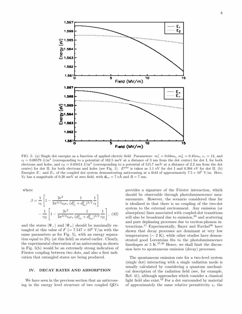
From Eq. 18 we see that an external field reduces theenergy E for both electrons and holes, with the shift be-ing greater for bigger dots. We therefore consider twocoupled dots of different material concentrations, withone of slightly greater dimensions and having a largerband-gap, and in Fig. 5(a) show that the single dot en-ergy levels cross (for our choice of parameters) as an elec-tric field is applied. Such a situation is plausible for sys-tems such as InGaAs where dot layers of varying indiumcontent, and hence varying band-gap, may be grown38
and it applies directly to the parameters chosen here(see also Sec. V below). Diagonalising the Hamiltonian(Eq. 26) as the field strength F varies gives us a modelprediction for the behaviour of the energy levels E− andE+ as shown in Fig. 5(b), where an anticrossing is ob-served at a field of approximately 7.5 × 10⁶ V/m. Sinceω1, ω2, and VF are all functions of F (as is also shownin Eqs. 18, 25 and 38) there is large scope for findingparameter regimes with interesting behaviour.
An analytical expression for the field strength at reso-nance can be calculated from the condition ∆ω = 0. Thetotal energy of each dot is given by
E = Egap +3~
2
(√c
m∗e
+
√c
m∗h
)− (eF )2
c−Meh, (39)
for identical potential wells in all directions for both elec-trons and holes (cx = cy = cz = c). When dot I and dotII are resonant
EI − EII = 0
= (EgapI − Egap
II ) +3~
2
[√cI
(1√m∗
e
+1√m∗
h
)
−√cII
(1√m∗
e
+1√m∗
h
)]
− (eF )2(
1
cI− 1
cII
)−MehI
+MehII, (40)
and therefore
F 2 =1
βe2
{(Egap
I − EgapII )
+3~
2
[(√cI −
√cII)
(1√m∗
e
+1√m∗
h
)]
− e2
2π3/2ǫ0ǫr
[1
(d2eI
+ d2hI
)1/2− 1
(d2eII
+ d2hII
)1/2
]},
(41)
8
FIG. 5: (a) Single dot energies as a function of applied electric field. Parameters: m∗e = 0.04m0, m∗
h = 0.45m0, ǫr = 12, andcI = 0.00579 J/m2 (corresponding to a potential of 162.5 meV at a distance of 3 nm from the dot centre) for dot I, for bothelectrons and holes, and cII = 0.03414 J/m2 (corresponding to a potential of 515.7 meV at a distance of 2.2 nm from the dotcentre) for dot II, for both electrons and holes (see Fig. 1). Egap is taken as 1.1 eV for dot I and 0.394 eV for dot II. (b)Energies E− and E+ of the coupled dot system demonstrating anticrossing at a field of approximately 7.5 × 10⁶ V/m. Here,VF has a magnitude of 0.20 meV at zero field, with dcv = 7 eA and R = 7 nm.
where
β =1
cI
[1 − 2e2
3π3/2ǫ0ǫr
1
(d2eI
+ d2hI
)3/2
1
cI
]
− 1
cII
[1 − 2e2
3π3/2ǫ0ǫr
1
(d2eII
+ d2hII
)3/2
1
cII
], (42)
and the states |Ψ−〉 and |Ψ+〉 should be maximally en-tangled at this value of F (= 7.547 × 10⁶ V/m with thesame parameters as for Fig. 5), with an energy separa-tion equal to 2VF (at this field) as stated earlier. Clearly,the experimental observation of an anticrossing as shownin Fig. 5(b) would be an extremely strong indication ofForster coupling between two dots, and also a first indi-cation that entangled states are being produced.
IV. DECAY RATES AND ABSORPTION
We have seen in the previous section that an anticross-ing in the energy level structure of two coupled QD’s
provides a signature of the Forster interaction, whichshould be observable through photoluminescence mea-surements. However, the scenario considered thus faris idealized in that there is no coupling of the two-dotsystem to the external environment. Any emission (orabsorption) lines associated with coupled-dot transitionswill also be broadened due to emission,39 and scatteringand pure dephasing processes due to exciton-phonon in-teractions.11 Experimentally, Bayer and Forchel36 haveshown that decay processes are dominant at very lowtemperatures (∼ 2 K), while other studies have demon-strated good Lorentzian fits to the photoluminescencelineshapes at 5 K.37,40 Hence, we shall limit the discus-sion here to spontaneous emission (decay) processes.
The spontaneous emission rate for a two-level system(single dot) interacting with a single radiation mode isusually calculated by considering a quantum mechani-cal description of the radiation field (see, for example,Ref. 41), although approaches which consider a classicallight field also exist.42 For a dot surrounded by materialof approximately the same relative permittivity ǫr the

9
decay rate becomes43
Γsp =√ǫrω3
10|Odcv|23πc3~ǫ0
, (43)
where ~ω10 is the energy difference of the two levels un-der consideration. For a typical InGaAs dot we take theparameters ω10 = 1.3 eV, Odcv = 6 eA, and ǫr = 12 togive Γsp = 1.04 × 10⁹ s−1 or a decay time of τdecay =1/Γsp = 964 ps, comparable with experimentally mea-sured exciton lifetimes in this system.35,36,37
Here, we are primarily interested in the properties oftwo interacting dots which form the four-level systemconsidered in Sec. III A. The various decay rates be-tween each level may be calculated in the same manneras for the two-level system previously considered, provid-ing that the changes in transition dipole moments due tothe interaction are properly accounted for. We will thenbe able to predict the typical linewidths that would beobserved in experimental measurements of these transi-tions. We characterize the dipole operator in the com-putational basis according to which dot the transitionoccurs within:
〈00| 〈01| 〈10| 〈11|0 OIIdcv(II) OIdcv(I) 0 |00〉
OIIdcv(II) 0 0 OIdcv(I) |01〉OIdcv(I) 0 0 OIIdcv(II) |10〉
0 OIdcv(I) OIIdcv(II) 0 |11〉
. (44)
Transitions such as |11〉 → |00〉 have zero dipole momentsince the corresponding integral is zero due to the orthog-onality of valence and conduction band wavefunctions oneach dot:
〈r〉 =
∫ψ∗
n(r1)ψ∗m(r2)(r1 + r2)ψ′
n(r1)ψ′m(r2)dr1dr2
=
∫ψ∗
n(r1)r1ψ′n(r1)dr1
∫ψ∗
m(r2)ψ′
m(r2)dr2
+
∫ψ∗
n(r1)ψ′n(r1)dr1
∫ψ∗
m(r2)r2ψ′m(r2)dr2
= 0. (45)
As a result of Eq. 44, we may express the dipole momentsfor general transitions such as a|01〉 ± b|10〉 → |00〉 by
〈r〉a,b = a〈00|r|01〉± b〈00|r|10〉 = aOIIdcv(II) ± bOIdcv(I),(46)
which may then be inserted directly into Eq. 43, alongwith the correct frequencies, to give the correspondingdecay rates. In Fig. 6 we plot Γsp for the two energycurves of Fig. 5 (b) from Eqs. 27, 43 and 46, and withthe same parameters as Fig. 5. A special case occurs foridentical dots at the anticrossing. Here, the symmetriceigenstate 2−1/2(|01〉 + |10〉) has a transition dipole mo-
ment to the ground state of√
2Odcv (OI = OII = O,dcv(I) = dcv(II) = dcv) and hence a decay rate of twicethat expected for a single dot. However, the antisymmet-ric eigenstate 2−1/2(|01〉 − |10〉) has no transition dipole
0 5 10 150.0
0.5
1.0
1.5
2.0
2.5
3.0
Field (MV/m)
Γ s
p (
10
9 s
−1)
FIG. 6: Spontaneous emission rates of the coupled-dot energylevels of Fig. 5. The dashed curve corresponds to the uppercurve in Fig. 5 (b); the solid curve corresponds to the lowercurve in Fig. 5 (b).
moment and consequently no spontaneous emission ratein the dipole approximation. This is otherwise known asa “dark” state and any spectral line corresponding to thistransition will display a characteristic narrowing and lossof intensity as the anticrossing is approached.
This effect may be studied in more detail by consid-ering the absorption lineshape of each transition (withinthe rotating-wave approximation):39,44
α(ω) =ωe2|〈r〉|2cη~ǫ0
(Γsp/2)
(ω10 − ω)2 + (Γsp/2)2, (47)
where η is the refractive index. Here, the only line broad-ening which is accounted for is due to spontaneous emis-sion. This leads to absorption lines with a Lorentziandependence on frequency, and a full width at half maxi-mum given by Γsp. Although other mechanisms may alsobroaden the lines, for example “pure” dephasing due toexciton-phonon interactions as mentioned earlier, theseprocesses can usually be reduced, in our case by coolingthe system.40 However, it is difficult to reduce the spon-taneous emission rate of a given transition. Therefore,the linewidth Γsp is the minimum achievable from anystandard dot sample and hence it is vitally important toensure that any effects we wish to observe will not bemasked by its presence.
Plotted in Fig. 7 are the absorption spectra of thetwo energy levels in Fig. 5(b) (E+ and E−) at fields of0, 5, 7, 10, 15 MV/m respectively, calculated from Eq. 47with the same parameters as for Fig. 5 and η = 3.46. Thespontaneous emission rates are calculated from Eq. 43and the peaks have been artificially broadened by a fac-tor of 10 to exaggerate their characteristic features inthe changing applied field. As the field is increased thetwo peaks shift to lower energies with the initially higher

10
FIG. 7: Series of simulated absorption spectra of the energylevels in Fig. 5(b) at fields of F = 0, 5, 7, 10, 15 MV/m. Theselines have been artificially broadened by a factor of 10.
energy line (corresponding to E+) shifting by a greateramount so that their separation reduces. The width ofthe lower energy line (E−) increases as the anticrossingpoint (F = 7.5 MV/m) is approached signifying its in-creasing decay rate (see Eq. 46). On the other hand,the width of the E+ line decreases as it approaches adark state, and the area underneath the curve is re-duced. This would correspond to a lowering of intensityof this line in a photoluminescence experiment. We cansee that the separation of the lines due to the Forsterinteraction (2VF ∼ 0.4 meV) is well resolved in the pres-ence of radiative broadening at low temperatures, andshould be so even if the lines have extra broadening due
to exciton-phonon interactions. In fact, sharp emissionlines of approximately 0.1 meV width have been obtainedfrom single InGaAs QD’s at a temperature of 100 K,36
indicating that up to this temperature at least, the an-ticrossing effect should still be observable. At very highfields (F = 10−15 MV/m) beyond the anticrossing pointthe two lines once again become well separated and even-tually have similar widths, indicating that the states |01〉and |10〉 are now only weakly coupled.
V. CONNECTION TO QUANTUM
INFORMATION PROCESSING
The experimental observation through photolumines-cence of an anticrossing of the type above would be asignificant step towards proof-of-principle experiments;although it could be a difficult experiment to perform,this method may well yield results more quickly than anattempt at coherent control on dot systems coupled inthis way.
The main question here is the feasibility of bringingtwo dots into resonance using a static external electricfield. As has been mentioned above, and can be seen inFig. 5(a), a larger dot experiences a larger shift in itsenergy levels due to the applied field than a smaller one.However, all other parameters being equal, a larger dotalso has slightly lower energy at zero field (which is notthe case in Fig. 5). Therefore, a way is needed of in-creasing the initial energy of the larger dot relative tothe smaller one. This could be realised by using layersof different materials (or material concentrations) to al-ter the band-gap within each dot; other methods suchas exploiting different dot geometries or applying a localstrain or electric field gradient should also be explored.In Ref. 29 field gradients close to 20 (MV/m)/µm weregenerated, with Stark shifts of approximately 2 meV ob-tained in a field of 0.2 MV/m. Hence, similar dots of1 − 2 meV initial energy separation, and placed 7 nmapart, could be brought into resonance by this method.Nitride QD’s could also offer a promising approach sincetheir strong piezoelectric fields allow the possibility ofan external field shifting their energy levels towards eachother.
We have also shown that it should be possible to engi-neer nanostructures such that the off-diagonal Forsterinteraction between a pair of QD’s is of the requiredstrength to make it interesting for quantum computation.Once a measurement of this coupling strength is made,the next logical step is to attempt to controllably entan-gle the excitonic states of two interacting dots, leading onto a demonstration of a simple quantum logic gate suchas the controlled-NOT (CNOT). Although, on resonance,the states |01〉 and |10〉 naturally evolve into maximallyentangled states after a time π/(4VF), their initializa-tion requires the inter-dot interaction to be suppressed.Furthermore, the generation of a logic gate such as theCNOT requires single qubit operations on both dots, as

11
well as periods of interaction.By switching to a pseudo-spin description of our ex-
citonic qubit we can immediately consider a previouslyknown operation sequence for the realization of a CNOTgate. Defining | ↑z〉 ≡ |0〉 and | ↓z〉 ≡ |1〉, we can seefrom Eq. 26 that the off-diagonal terms can be expressedas
HF =VF
2(σx1
σx2+ σy1
σy2) , (48)
with
σx =
(0 11 0
)and σy =
(0 −ii 0
), (49)
being two of the Pauli spin matrices. This XY typeHamiltonian has been studied in the literature for varioussystems45,46 and if the two interacting qubits are left fora time t = π/(2VF ) solely under its influence then aniSWAP gate will be executed:47
iSWAP =
1 0 0 00 0 i 00 i 0 00 0 0 1
, (50)
in the basis {|00〉, |01〉, |10〉, |11〉}. Two iSWAP opera-tions may be concatenated with single qubit operationsto form the more familiar CNOT gate:
CNOT =(π
2
)
x2
(π2
)
z2
(−π
2
)
z1
(iSWAP)(π
2
)
x1
× (iSWAP)(π
2
)
z2
, (51)
where (±π/2)lm are single pseudo-spin rotations of ±π/2about the l axis of spin m, for l = x, z and m = 1, 2.Schuch and Siewert47 have also shown that the CNOTand SWAP operations may be combined when using anXY interaction to produce more efficient quantum cir-cuits. Furthermore, the iSWAP operation is an entan-gling gate and is therefore sufficient for universal quan-tum computation provided that fast local unitary opera-tions are available. In fact, for systems exhibiting an XYinteraction, the iSWAP operation constitutes the natu-ral gate choice when implementing efficient quantum cir-cuits.
To perform a gate such as the CNOT outlined abovewe must be able to control the interaction between ourtwo qubits so that we can effectively switch it off for theduration of the single qubit manipulations. For the caseof excitonic qubits, coupled via the Forster mechanism,the most sensible way to proceed is to consider two ini-tially non-resonant QD’s with negligible energy transfer.Single qubit operations can then be achieved with ex-ternal laser pulses by inducing Rabi oscillations withineach dot.48 As each dot will have a different excitationenergy, we may address them individually by choosingthe appropriate frequency. Two periods of free evolu-tion under the interaction Hamiltonian (Eq. 48) are also
required; applying a suitably selected detuned pulse toboth non-resonant dots will bring them into resonancevia the optical Stark effect.49,50 We then allow resonantenergy transfer to occur for a time t = π/(2VF) producingan iSWAP operation. The detuned pulse is then stoppedand single qubit manipulations may be induced as before.
Figure 5(b) provides a nice visualisation of the wholeprocess. We must non-adiabatically switch between thetwo regimes of zero field, where the dots are effectivelyuncoupled, and the resonant point where the dots inter-act. It is our hope that this is achievable through theoptical Stark effect, and we speculate that this all opti-cal approach may have the potential to allow gates to beperformed well within the limits set by the nanoseconddephasing times experimentally observed.
To summarise, we have analytically calculated themagnitude of the Forster energy transfer between a pairof generic QD’s and investigated its effect on their energylevel structure. We have proposed a simple experimentwhich provides a signature of the interaction and an esti-mate of its strength, and have also discussed its possibleapplication to quantum information processing.
Acknowledgments
AN, BWL, and JHR are supported by EPSRC (BWLand JHR as part of the Foresight LINK Award Nanoelec-
tronics at the Quantum Edge, www.nanotech.org). BWLthanks St Anne’s College for support. SDB acknowl-edges support from the E.U. NANOMAGIQC project(Contract no. IST-2001-33186); We thank T. P. Spiller,W. J. Munro, S. C. Benjamin and R. A. Taylor for stim-ulating discussions.
APPENDIX: TUNNELING
To outline the effect of electron and hole tunnel-ing on the exciton states used in this paper, we con-sider here the Hamiltonian for an electron-hole pairin a double-dot. The basis we use is constructed ofproducts of the electron and hole single-particle states{|eIhI〉, |eIhII〉, |eIIhI〉, |eIIhII〉}, which gives
H =
EeIhIth te VF
th EeIhII0 te
te 0 EeIIhIth
VF te th EeIIhII
, (A.1)
where Eenhm= Een
+ Ehm−Menhm
, with n,m = I, IIfor dot I and dot II respectively. Menhm
is the directCoulomb binding energy between the electron and holeon dot n andm respectively, and the band-gap energy hasbeen absorbed into the electron energy Een
by setting theenergy zero to be at the top of the valence band. VF isthe Forster interaction strength, and te(h) is the electron(hole) tunneling matrix element.
12
We consider first the simple case of two identical dotscoupled to one another; this means setting EeI
= EeII≡
Ee, EhI= EhII
≡ Eh, MeIhI= MeIIhII
≡ Meh, andMeIhII
= MeIIhI≡ M ′
eh. Subtracting Ee + Eh − Meh
from the diagonal of Eq. A.1 gives
H =
0 th te VF
th Meh −M ′eh 0 te
te 0 Meh −M ′eh th
VF te th 0
. (A.2)
We would like to isolate the {|eIhI〉, |eIIhII〉} subspace,as it is composed of single exciton states on each of thetwo dots. These states are exactly the ones that are rel-evant for the computational basis introduced in Sec. I.Any leakage from this subspace, potentially due to tun-nel couplings to the states |eIhII〉 and |eIIhI〉, could be asource of error for the signature and schemes presentedhere and in Refs. 8,26 and must be minimized. However,under the condition
|Meh −M ′eh| ≫ |te|, |th|, (A.3)
we may use degenerate perturbation theory on Eq. A.2to give
Heff =
− t2e+t2
h
Meh−M ′
eh
VF − 2teth
Meh−M ′
eh
VF − 2teth
Meh−M ′
eh
− t2e+t2
h
Meh−M ′
eh
, (A.4)
in the {|eIhI〉, |eIIhII〉} subspace. Hence, the states |eIhI〉and |eIIhII〉 are still resonantly coupled in the presenceof tunneling as long as Eq. A.3 is satisfied. Theseconditions are better satisfied as the inter-dot separa-tion increases (tunneling elements consequently reduce,as does M ′
eh so that |Meh − M ′eh| becomes larger),
and as dot confinement increases (tunneling elementsreduce, Meh increases so that |Meh − M ′
eh| again be-comes larger). Furthermore, corrections to the eigen-states |χ±〉 ≡ 2−1/2(|eIhI〉 ± |eIIhII〉) due to mixing with
states outside the subspace will be small since they areweighted by factors of te(h)/(M
′eh −Meh), to first order,
from the perturbation theory.
The regime in which Eq. A.2 is valid is not necessar-ily the ideal one for minimizing the effect of tunneling,while exploiting resonant exciton interactions, as twonon-identical dots may also be brought into resonance(see Section III C). In this case, EeI
+ EhI− MeIhI
=EeII
+ EhII−MeIIhII
≡ E on resonance. Subtracting Efrom the diagonal of Eq. A.1 gives
H =
0 th te VF
th ∆Eh + ∆Mh 0 tete 0 ∆Ee + ∆Me thVF te th 0
, (A.5)
where ∆Ei = EiII − EiI , for i = e, h, and ∆Mh =MeIhI
−MeIhII, ∆Me = MeIhI
−MeIIhI. The dots must
now satisfy the modified condition
min(|∆Eh + ∆Mh|, |∆Ee + ∆Me|) ≫ |te|, |th|, (A.6)in order for tunneling to be neglected, with the unwantedstates |eIhII〉 and |eIIhI〉 weighted by a factors of magni-tude
te(h)
|∆Eh + ∆Mh|, (A.7)
and
te(h)
|∆Ee + ∆Me|, (A.8)
to first order in a perturbation expansion. Again, tunnel-ing will be suppressed as dot separation and confinementincreases.
∗ Electronic address: [email protected]† On leave of absence from Centro Internacional de Fısica
(CIF), A.A. 4948, Bogota, Colombia1 See e.g. the special issue on quantum dots for quantum
computing, edited by H. Matsueda and J. P. Dowling, Su-perlattices and Microstr. 31 73, (2002).
2 E. Biolatti, I. D’Amico, P. Zanardi, and F. Rossi,Phys. Rev. B 65, 075306 (2002).
3 T. Forster, Discuss. Faraday Soc. 27, 7 (1959).4 C. R. Kagan, C. B. Murray, M. Nirmal, and M. G.
Bawendi, Phys. Rev. Lett. 76, 1517 (1996).5 S. A. Crooker, J. A. Hollingsworth, S. Tretiak, and V. I.
Klimov, Phys. Rev. Lett. 89, 186802 (2002).6 A. J. Berglund, A. C. Doherty, and H. Mabuchi, Phys.
Rev. Lett. 89, 068101 (2002).7 X. C. Hu, T. Ritz, A. Damjanovic, F. Autenrieth, and
K. Schulten, Q. Rev. Biophys. 35, 1 (2002).8 B. W. Lovett, J. H. Reina, A. Nazir, B. Kothari, and
G. A. D. Briggs, Phys. Lett. A 315, 136 (2003).9 L. Quiroga and N. F. Johnson, Phys. Rev. Lett. 83, 2270
(1999); J. H. Reina, L. Quiroga, and N. F. Johnson, Phys.Rev. A 62, 012305 (2000).
10 D. L. Dexter, J. Chem. Phys. 21, 836 (1953).11 B. Krummheuer, V. M. Axt, and T. Kuhn, Phys. Rev. B
65, 195313 (2002).12 I. D’Amico and F. Rossi, Appl. Phys. Lett. 79, 1676 (2001).13 L. Jacak, P. Hawrylak, and A. Wojs, Quantum Dots
(Springer-Verlag, Heidelberg, 1998).14 D. J. Eaglesham and M. Cerullo, Phys. Rev. Lett. 64, 1943
(1990).15 Q. Xie, A. Madhukar, P. Chen, and N. P. Kobayashi,
Phys. Rev. Lett. 75, 2542 (1995).

13
16 J. Tersoff, C. Teichert, and M. G. Lagally, Phys. Rev. Lett.76, 1675 (1996).
17 M. Califano and P. Harrison, J. Appl. Phys. 86, 5054(1999).
18 S. Gangopadhyay and B. R. Nag, Nanotechnology 8, 14(1997).
19 M. V. RamaKrishna and R. A. Friesner, Phys. Rev. Lett.67, 629 (1991).
20 L. W. Wang and A. Zunger, J. Phys. Chem 98, 2158(1994).
21 A. Franceschetti and A. Zunger, Phys. Rev. Lett. 78, 915(1997).
22 G. Bastard, Phys. Rev. B 24, 5693 (1981).23 P. Harrison, Quantum Wells, Wires and Dots (Wiley, New
York, 2001).24 G. W. Bryant, Phys. Rev. B 37, 8763 (1988).25 D. B. TranThoai, Y. Z. Hu, and S. W. Koch, Phys. Rev.
B 42, 11261 (1990).26 B. W. Lovett, J. H. Reina, A. Nazir, and G. A. D. Briggs,
Phys. Rev. B 68, 205319 (2003).27 A. Franceschetti, H. Fu, L. W. Wang, and A. Zunger, Phys.
Rev. B 60, 1819 (1999).28 L. I. Schiff, Quantum Mechanics (McGraw-Hill, New York,
1955), 2nd ed.29 R. Rinaldi, M. DeGiorgi, M. DeVittorio, A. Melcarne,
P. Viscontia, R. Cingolani, H. Lipsanen, M. Sopanen,T. Drufva, and J. Tulkki, Jpn. J. Appl. Phys. 40, 2002(2001).
30 W. Heller, U. Bockelmann, and G. Abstreiter, Phys. Rev.B 57, 6270 (1998).
31 S. Seufert, M. Obert, M. Scheibner, N. A. Gippius,G. Bacher, A. Forchel, T. Passow, K. Leonardi, andD. Hommel, Appl. Phys. Lett. 79, 1033 (2001).
32 W. Sheng and J.-P. Leburton, Phys. Rev. B 67, 125308(2003).
33 K. L. Silverman, R. P. Mirin, S. T. Cundiff, and A. G.Norman, Appl. Phys. Lett. 82, 4552 (2003).
34 P. G. Eliseev, H. Li, A. Stintz, G. T. Lin, T. C. Newell,K. J. Malloy, and L. F. Lester, Appl. Phys. Lett. 77, 262(2000).
35 P. Borri, W. Langbein, S. Schneider, U. Woggon, R. L.
Sellin, D. Ouyang, and D. Bimberg, Phys. Rev. Lett. 87,157401 (2001).
36 M. Bayer and A. Forchel, Phys. Rev. B 65, 041308(R)(2002).
37 D. Birkedal, K. Leosson, and J. M. Hvam, Phys. Rev. Lett.87, 227401 (2001).
38 Q. Zhang, J. Zhu, X. Ren, H. Li, and T. Wang,Appl. Phys. Lett. 78, 3830 (2001).
39 R. Loudon, The quantum theory of light (Oxford Univer-sity Press, New York, 1986), 2nd ed.
40 P. Borri, W. Langbein, U. Woggon, M. Schwab, M. Bayer,S. Fafard, Z. Wasilewski, and P. Hawrylak, Phys. Rev.Lett. 91, 267401 (2003).
41 P. K. Basu, Theory of optical processes in semiconductors
(Oxford University Press, Oxford, 1997).42 S. V. Goupalov, Phys. Rev. B 68, 125311 (2003).43 A. Thranhardt, C. Ell, G. Khitrova, and H. M. Gibbs,
Phys. Rev. B 65, 035327 (2002).44 H. Haug and S. W. Koch, Quantum theory of the optical
and electric properties of semiconductors (World Scientific,Singapore, 1994), 3rd ed.
45 J. Siewert, R. Fazio, G. M. Palma, and E. Sciacca, J. LowTemp. Phys. 118, 795 (2000).
46 A. Imamoglu, D. D. Awschalom, G. Burkard, D. P. Di-Vincenzo, D. Loss, M. Sherwin, and A. Small, Phys. Rev.Lett. 83, 4204 (1999).
47 N. Schuch and J. Siewert, Phys. Rev. A 67, 032301 (2003).48 H. Kamada, H. Gotoh, J. Temmyo, T. Takagahara, and
H. Ando, Phys. Rev. Lett. 87, 246401 (2001).49 C. Cohen-Tannoudji, J. Dupont-Roc, and G. Grynberg,
Atom-photon Interactions: Basic Processes and Applica-
tions (Wiley, New York, 1992).50 A. Nazir, B. W. Lovett, and G. A. D. Briggs, Phys. Rev.
A 70, 052301 (2004).51 With this choice of potential we are able to model both
the convenient situation of a spherically symmetric QD,and the more common situation in self-assembled dots ofstronger confinement in the growth (z) direction than inthe x, y plane.
Copyright © 2022 FDOKUMEN