Quantum Transport in Graphene Nanoribbons with Realistic Edges
Upload
independentCategory
view
2download
0
Transport properties of graphene quantum dots
J. W. Gonzalez and M. PachecoDepartamento de Fısica, Universidad Tecnica Federico Santa Marıa, Casilla 110 V, Valparaıso, Chile
L. Rosales*
Departamento de Fısica, Universidad Tecnica Federico Santa Marıa, Casilla 110 V, Valparaıso, Chile andInstituto de Fısica, Pontificia Universidad Catolica de Valparaıso, Casilla 4059, Valparaıso, Chile
P. A. OrellanaDepartamento de Fısica, Universidad Catolica del Norte, Casilla 1280, Antofagasta, Chile
(Dated: April 6, 2011)
In this work we present a theoretical study of transport properties of a double crossbar junctioncomposed by segments of graphene ribbons with different widths forming a graphene quantumdot structure. The systems are described by a single-band tight binding Hamiltonian and theGreen’s function formalism using real space renormalization techniques. We show calculations ofthe local density of states, linear conductance and I-V characteristics. Our results depict a resonantbehavior of the conductance in the quantum dot structures which can be controlled by changinggeometrical parameters such as the nanoribbon segments widths and relative distance between them.By applying a gate voltage on determined regions of the structure, it is possible to modulate thetransport response of the systems. We show that negative differential resistance can be obtained forlow values of gate and bias voltages applied.
PACS numbers: 61.46.-w, 73.22.-f, 73.63.-b
I. INTRODUCTION
In the last few years, graphene-based systems haveattracted a lot of scientific attention. Graphene is asingle layer of carbon atoms arranged in a two dimen-sional hexagonal lattice. In the literature, it has beenreported several experimental techniques in order to ob-tain this crystal, such as mechanical peeling or epitax-ial growth2–4. On the other hand, graphene nanoribbons(GNRs) are stripes of graphene which can be obtained bydifferent methods like high-resolution lithography5, con-trolled cutting processes6 or by unzipping multiwalledcarbon nanotubes7. Different graphene heterostructuresbased on patterned GNRs have been proposed and con-structed, such as graphene junctions8, graphene flakes9,graphene antidots superlattices10, and graphene nano-constrictions11. The electronic and transport prop-erties of these nanostructures are strongly dependentof their geometric confinement, allowing the possibil-ity to observe quantum phenomena like quantum inter-ference effects, resonant tunneling and localization. Inthis sense, the controlled modification of these quan-tum effects by means of external potentials which changethe electronic confinement, could be used to developnew technological applications such as graphene-basedcomposite materials12, molecular sensor devices13,14 andnanotransistors15.
In this work we study the transport proper-ties of quantum-dot like structures, formed by seg-ments of graphene ribbons with different widths con-nected between each other, forming a double crossbarjunction18,19. These graphene quantum dots (GQDs)could be versatile experimental systems which allow a
FIG. 1: Schematic view of a GQD structure based on leadsof width NL = 9, and a conductor region composed by twosymmetrical junctions of width NB = 21 and length LB = 3separated by a central structure of length LC = 4 and widthNC = 9
range of operational regimes from conventional single-electron detectors to ballistic transport. The systems wehave considered are conductors formed by two symmet-ric crossbar junctions of widths NB and length LB , anda central region that separates the junctions, of widthNC and length LC . Two semi-infinite leads of widthNL = NC are connected to the ends of the central con-ductor. A schematic view of the considered system ispresented in figure 1. We studied the different electronicstates appearing in the system as a function of the ge-ometrical parameters of the GQD structure. We foundthat the GQD local density of states (LDOS) as a func-tion of the energy shows the presence of a variety of sharppeaks corresponding to localized states and also statesthat contributes to the electronic transmission which aremanifested as resonances in the linear conductance. By
arX
iv:1
104.
0709
v1 [
cond
-mat
.mes
-hal
l] 4
Apr
201
1

2
changing the geometrical parameters of the structure, itis possible to control the number and position of theseresonances as a function of the Fermi energy. On theother hand a gate voltage applied at selected regions ofthe conductor allows the modulation of their transportproperties exhibiting a negative differential conductance(NDC) at low values of the bias voltage.
II. MODEL
All considered systems have been described by usinga single π-band tight binding hamiltonian, taking intoaccount nearest neighbor interactions with a hoppingparameter γ0 = 2.75 eV . Besides, we have consideredhydrogen passivation by setting a different hopping pa-rameter for the carbon dimers at the ribbons edges20,γedge = 1.12γ0 .
The electronic properties of the systems have been cal-culated using the surface Green’s functions matching for-malism (SGFMF)14,22. In this scheme, we divide theheterostructure in three parts, two leads composed bysemi-infinite pristine GNRs, and the conductor regioncomposed by the double GNRs crossbar junctions, as itis shown in figure 1.
In the linear response approach, the electronic conduc-tance is calculated by the Landauer formula. In terms ofthe conductor Green’s functions, it can be written as23:
G =2e2
hT (E) =
2e2
hTr[ΓLG
RCΓRG
AC
], (1)
where T (E), is the transmission function of an electron
crossing the conductor region, ΓL/R = i[ΣL/R − Σ†L/R]
is the coupling between the conductor and the respec-tive leads, given in terms of the self-energy of each lead:ΣL/R = VC,L/R gL/R VL/R,C . Here, VC,L/R are the cou-pling matrix elements and gL/R is the surface Green’s
function of the corresponding lead14. The retarded (ad-vanced) conductor Green’s function are determined by23:
GR,AC = [E −HC − ΣR,AL − ΣR,AR ]−1 (2)
where HC is the hamiltonian of the conductor. In orderto calculate the differential conductance of the systems,we determine the I-V characteristics by using the Lan-dauer formalism23. At zero temperature, it reads
I (V ) =2e
h
µ0+V/2∫µ0−V/2
T (E, V ) dE, (3)
where µ0 is the chemical potential of the system in equi-librium and T (E, V ) is defined by equation (1). TheGreen’s functions and the coupling terms depend on theenergy and the bias voltage. We consider a linear volt-age drop along the longitudinal direction of the conductorand the gate voltage is included in the on-site energy at
the regions in which this potential is applied. In what fol-lows the Fermi energy is taken as the zero energy level,all energies are written in terms of the hopping param-eter γ0 and the conductance is written in units of thequantum of conductance G0 = 2e2/h.
III. RESULTS AND DISCUSSION
In figure 2, we display results of the linear conductancefor a graphene quantum dot structure formed by twoarmchair ribbons leads of width NL = 5 and a conductorregion composed by two symmetric crossbar junctions ofwidth NB = 17 and variable lengths LB (from 1 up to 7). Two relative distances between the junctions: panel (a)LC = 5 and panel (b) LC = 10 are considered and theconductance of a pristine NL = 5 armchair nanoribbonis included as a comparison (light green dotted line).
In both panels it is possible to observe a series of peaksat defined energies in the conductance curves. This res-onant behavior of the electronic conductance arises fromthe interference of the electronic wave functions insidethe structure, which travel forth and back forming sta-tionary states in the conductor region (well-like states).In order to understand these results, it is convenient todefine two energy regions, the low-energy range from 0up to 0.7 γ0 (corresponding to the first quantum of con-ductance for the pristine N = 5 armchair ribbon) andthe high-energy range, from 0.7 to 1.2 γ0 (correspondingto the second step of conductance of the N = 5 pristinesystem).
In the low-energy range, it is clear that the conduc-tance peaks correspond to resonant states belonging tothe central region of the conductor. By increasing therelative distance LC of the central part of the system,the number of allowed well-like states also increases and,as a consequence, the conductance curves exhibit moreresonances14,18,24. The well-like states remain almost in-variant under geometrical modifications of the crossbarjunctions. However, for certain energy ranges and forparticular junction lengths, the electronic transmission ofthe systems. exhibits an almost constant value. For in-stance, in both panels of figure 2, for the cases of LB = 1and LB = 4 at the energy range 0.4 to 0.65 γ0. This effectcorresponds to a constructive interference between well-like states from the central region with states belongingto the crossbar junctions regions. The different inter-ference effects will be clarified by analyzing the LDOSof these systems, which is shown next in this paper. Inthe high-energy region, the conductance curves exhibit acomplex behavior as a function of the geometrical param-eters of the GQD structures. There is not a predictablebehavior of the conductance as the width and length ofthe crossbar junction are increased.
It is important to pointed out, from the analysis offigure 2, that it is possible to identify some interestingeffects associated to well known quantum phenomena.For instance, in panels (a) and (b) of figure 2, for the

3
FIG. 2: Conductance as a function of the Fermi energy for agraphene quantum dot structure composed by two armchairribbons leads of width NL = 5, a double symmetric crossbarjunctions of width NB = 17 and variable length, from LB = 1up to LB = 7. The central region has a width NC = 5and two separations (a) LC = 5 and (b) LC = 10. Lightgreen dotted line corresponds to the conductance of a pristineNL = 5 ribbon. All curves have been shifted 2G0 for a bettervisualization.
cases LB = 5, 6 and 7 at energies around E = 0.5γ0, itis possible to observe a non-symmetric line shape, whichcorresponds to a convolution of a Fano-like25 and a Breit-Wigner26 resonances. This kind of line-shape, has beenobserved before in other mesoscopic systems by Orellanaand co-workers27. In that reference, a simple model oftwo localized states with the same energy ωc are directlycoupled between each other by a coupling τ and indi-rectly coupled throughout a common continuum. Thecorresponding resonances have been adjusted by usingthe following expression:
T (ω) =4η2[(ω − ωc)x− τ ]2
[(1 − x2)η2 − (ω − ωc)2 + τ2]2 + 4(ω − ωc − τx)2
(4)where η is the width of a localized state coupled to the
FIG. 3: (Color online) Numerical adjustment of a convolutionof a Fano and a Breit -Wigner line shapes (red dash line) andone of the conductance resonance in the system (black solidline) with η = 0.01γ0, ωc = 0.59γ0, x=0.7,τ = 0.02γ0.
continuum and x defines the degree of asymmetry of thesystem.
We realize that a possible interference mechanism oc-curring in our considered system can be explained withthe above model, which helps to get an intuitive under-standing of the origin of some conductance lines shape.In figure 3 we have plotted a particular conductance res-onance and the corresponding fitting given by the modelrepresented by equation (4), where it is observed the goodagreement between both curves.
In what follows we focus our analysis on the resonantbehavior exhibited by the conductance curves, analyz-ing the different electronic states in the conductor. Wehave performed calculations of the spatial distributionof LDOS for certain energies corresponding to differentstates present in the conductor. In the bottom panel offigure 4 we show results for the LDOS as a function of theFermi energy, for a GQD structure formed by a doublecrossbar junction of width NB = 17 and length LB = 3,separated by a central region of width NC = 5 and lengthLC = 5.
We start our analysis focusing on the some sharp statespresent in the curve LDOS vs energy of this figure. Wehave marked the first three sharp states in this LDOSplot with the letters (a), (b) and (c) and we have calcu-lated the spatial distribution of these states, representingby the corresponding contour plots exhibited in the fig-ure. These states are completely localized at the crossbarjunctions, and as we establish in a previous work31, theircorrespond to bound states in the continuum (BICs)28–30.It is not expected that these kind of states play a role inthe electronic transport of these GQD structures, whichis shown at the corresponding conductance curves of fig-

4
FIG. 4: LDOS for a GQD formed by a double crossbar junc-tion of width NB= 17 and length LB= 3 separated by a cen-tral region of width NC= 5 and length LC=5. Panel (a),(b) and (c) correspond to the contour plots of some sharpLDOS resonances marked in the bottom plot. As a reference,the LDOS of a pristine N=5 armchair ribbon is plotted as adotted green line
ure 2.In what follows we will focus our analysis to those
states that contribute to the conductance of the systems.In figure 5 it is shown the spatial distribution of LDOSfor a GQD formed by a double crossbar junction of widthNB = 17 and length LB = 3, separated by a central re-gion of width NC = 5 and length LC = 5. As a reference,at the bottom panel we have included a plot with theLDOS versus Fermi energy of the GQD system, there wehave marked with letters (a), (b), (c) and (d) four partic-ular energy states. The corresponding contour plots aredisplayed at the upper part of the figure.
In these plots, it is possible to observe the resonant be-havior of these states, which are completely distributedalong the GQD structure, presenting a maximum of theprobability density at the center of the system. This con-dition favors the alignment of the electronic states of the
FIG. 5: LDOS for a GQD structure formed by a double cross-bar junction of width NB= 17 and length LB= 3 separatedby a central region of width NC= 5 and length LC=5. Panel(a),(b), (c) and (d) correspond to the contour plots of thoseresonant states marked in the LDOS plot displayed at thebottom.
leads with the resonant states in the conductor and con-sequently, a unitary transmission at those energy valuesis expected. This behavior is reflected as a series of reso-nant peaks in the conductance of the system that couldbe controlled by means of the geometrical parameters ofthe GQD, as it is shown in figure 2. At higher energiesthere is an interplay between localized states in the cross-bar junctions and resonant states in the central region ofthe conductor. As it is shown in panel (d) of figure 5,

5
FIG. 6: Conductance as a function of Fermi energy and gate voltage for GQDs composed by leads of width NL = 5, twocrossbar junctions of width NB = 17, a central part of width NC = 5 and length LC = 5. Panels (a) and (c) correspond tojunctions of length LB = 2, while panels (b) and (d) correspond to junctions of length LB = 3. In the upper panels the gatevoltage is applied at the crossbar regions, and in the lower panels the gate voltage is applied at the central structure. The blacksegmented lines highlight different slopes discussed in the text
some states are strongly dependent of the geometry ofthe junctions, therefore for some particular configurationit is possible to observe a non-null transmission at theseenergies, while for other cases, there are destructive inter-ference mechanisms that suppress completely the trans-mission at that energy region.
We have studied different configurations of GQDsstructures, varying systematically some geometric pa-rameters. We have observed a quite general behavior ofsuch resonant conductors with the presence of sharp andresonant states. Depending of each particular system, itcan be observed changes in the number and position inenergy of these states, as well as in their spatial distri-bution. The different intensity of the peaks in the LDOScurves depends on the spatial distribution of the states.There are states completely extended along the conduc-tor (like in panel (b) of figure 5 ) which generate widerand less intense peaks. On the other hand, there areresonant states which are more concentrated in certainregions of the conductor (like as panel (c) and (d) of fig-ure 5) which generate sharper and more intense peaks inthe LDOS.
Now we focus our analysis on the effects of an appliedgate voltage on the transport properties of GQD struc-tures. Results of the conductance as a function of theFermi energy, for different values of a gate voltage ap-plied in selected regions of a GQD are shown in figure6. The systems are composed by leads of width NL = 5,two crossbar junctions of width NB = 17, a central partof width NC = 5 and length LC = 5. Panels (a) and (c)correspond to junctions of length LB = 2, while panels(b) and (d) correspond to junctions of length LB = 3. Fi-nally, upper panels correspond to a gate voltage appliedat the crossbar junctions regions, whereas the lower pan-
els correspond to a gate voltage applied at the centralpart of the structure.
In these contour plots of conductance, it is possible toobserve the behavior of the resonant states of the sys-tem with a gate voltage applied at different regions ofthe structure. The lower panels of the figure 6 show thecase of a gate voltage applied at the central region of theconsidered GQDs. In these plots the linear dependenceof the conductance resonances as a function of the gatevoltage is manifested. It can be shown that the electronicstates of a pristine armchair graphene ribbon are regu-larly spaced in the whole energy range16,17, therefore, asthe gate voltage is applied, there will be a high probabil-ity that the lead states become aligned with the resonantstates in the central region of the structure. This behav-ior in completely general and independent of the widthLB of the crossbar junctions. The linear behavior of theconductance peaks could be useful in nanoelectronics de-vices, due to the possibility of control the current flowthrough these systems. This argument will be more clearwith the analysis of the differential conductance, whichis shown below in this paper.
The case of a gate voltage applied at the crossbar junc-tion regions is shown in the upper panel of figure 6. Theconductance behavior in more complicated to analyze,nevertheless it is still possible to observe a linear de-pendence of the resonant states with the gate voltage.However, two different slopes can be noticed, for statesbelonging to the crossbar junctions (lower slope) and forstates belonging to the central region of the conductor(higher slope). Besides, the panels exhibit an importantreduction in the conductance gap, for different values ofgate voltage. This effect is mainly produced by an en-ergy shift of the localized states at the junctions, which

6
induces a less destructive interference with the resonantstates. It is important to point out that this effect onlycan be observed because the gate potential is applied si-multaneously to both crossbar junctions, otherwise, theconductance gap would be not noticeably affected by thegate potential. Finally, the dark (blue online) regionspresent in figure 6, occur at energy ranges around theLDOS singularities of the pristine N=5 AGNR. At theseenergies, it appear the second and the third allowed statesappear, which interrupt the linear behavior of the con-ductance resonances as a function of the gate voltage.
In order to understand the presence of two differentslopes in the upper panel of figure 6, we present a simplemodel which keeps the underlying physics of the con-sidered system and allow us to explain qualitatively ourresults.
FIG. 7: A simple model of two crossbar junctions formed bytwo quantum dots, coupled to a linear chain of sites.
The scheme showed in figure 7 is a simple represen-tation of our conductor. The system is composed by alinear chain of three sites, which are connected to twosemi-infinite leads. We have considered four quantumdots connected to the extremes of the chain forming adouble crossbar junction, at which we have applied sym-metrically a gate voltage Vg. This potential will modifythe on-site energy of the dots by a linear shift of energyproportional to the gate voltage amplitude.
By using Dyson equation, it is possible to calculate theGreen’s function of the central site of the chain labeledby 0, which takes the form:
G00 =1
ω − ε0 − Σ(5)
where ω is the energy of the incident electrons, ε0 is thecentral on-site energy and the self energy Σ is given bythe following expression (see Appendix for a detailed de-duction):
Σ =v2(
ω − v2
ω−Vg
)2
+ Γ2
[(ω − v2
ω − Vg
)+ iΓ
](6)
In this model, the self energy of the Green’s functionsof the central region acquires a real part that dependson the gate voltage applied to the crossbar junction re-gion. As a consequence, two different slopes appear in
the behavior of the conductance peaks as a function ofthe gate voltage. One of these slopes corresponds to thedirect evolution of the states belonging to the crossbarjunctions as a function of the gate voltage (lower slope),and the higher slope corresponds to the indirect statesbelonging to the central region.
FIG. 8: (a) Current versus bias voltage and (b) Differentialconductance as a function of bias voltage for a GQD composedby two crossbar junctions of length LB = 2 and width NB =17 separated by a central region of width NC = 5 and avariable length from LC = 1 up to LC = 20. All curves havebeen shifted for a better visualization.
Now we focus our analysis on the I-V characteristicsand the differential conductance of these resonant GQDs.Figure 8 shows results of these transport properties fora conductor formed by two crossbar junctions of widthNB = 17, length LB = 2 and a central region of widthNC = 5. In this plots the length of the central struc-ture is varied from LC = 1 up to LC = 20. In panel (a)it is possible to observe that for a very small separationbetween both junctions, the I-V characteristics exhibitabrupt slope changes, and oscillations for certain rangesof the bias voltage. This behavior is produced by theincreasing number of resonant states as a result of theenlargement of the conductor central region. The ap-plied bias voltage allows the continuum alignment of theresonant states of the system with the electronic states ofthe leads, leading to variations of the current intensity.On the other hand, every I-V curve shows a wide gapof zero current until certain bias voltage. This thresholdvalue exhibits a linear dependence of the length of thecentral region of the conductor. As the relative distancebetween the junctions is increased, there are more reso-nant states available at lower energies because the elec-tronic confinement in this region is weaker, therefore, theelectronic transmission under a bias voltage is possible atlower voltage values.
The abrupt changes of the current as a function ofthe bias voltage are clearly reflected in the differentialconductance of these systems. In panel (b) of figure 8 it is
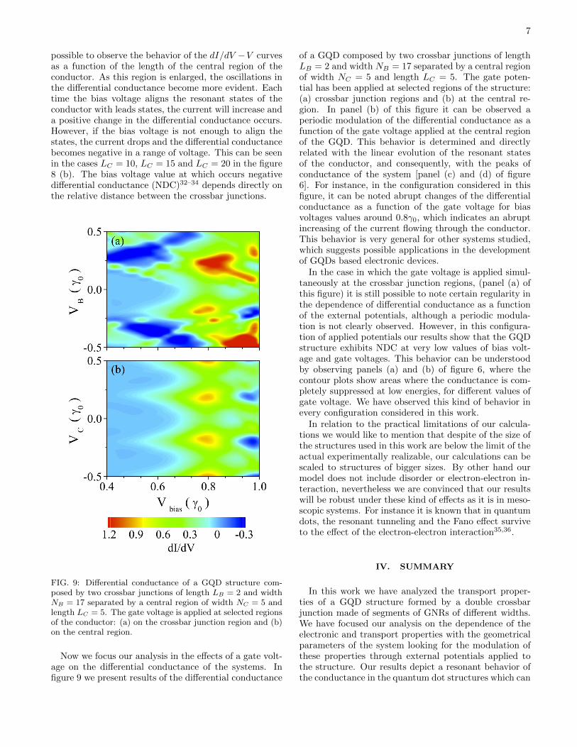
7
possible to observe the behavior of the dI/dV −V curvesas a function of the length of the central region of theconductor. As this region is enlarged, the oscillations inthe differential conductance become more evident. Eachtime the bias voltage aligns the resonant states of theconductor with leads states, the current will increase anda positive change in the differential conductance occurs.However, if the bias voltage is not enough to align thestates, the current drops and the differential conductancebecomes negative in a range of voltage. This can be seenin the cases LC = 10, LC = 15 and LC = 20 in the figure8 (b). The bias voltage value at which occurs negativedifferential conductance (NDC)32–34 depends directly onthe relative distance between the crossbar junctions.
FIG. 9: Differential conductance of a GQD structure com-posed by two crossbar junctions of length LB = 2 and widthNB = 17 separated by a central region of width NC = 5 andlength LC = 5. The gate voltage is applied at selected regionsof the conductor: (a) on the crossbar junction region and (b)on the central region.
Now we focus our analysis in the effects of a gate volt-age on the differential conductance of the systems. Infigure 9 we present results of the differential conductance
of a GQD composed by two crossbar junctions of lengthLB = 2 and width NB = 17 separated by a central regionof width NC = 5 and length LC = 5. The gate poten-tial has been applied at selected regions of the structure:(a) crossbar junction regions and (b) at the central re-gion. In panel (b) of this figure it can be observed aperiodic modulation of the differential conductance as afunction of the gate voltage applied at the central regionof the GQD. This behavior is determined and directlyrelated with the linear evolution of the resonant statesof the conductor, and consequently, with the peaks ofconductance of the system [panel (c) and (d) of figure6]. For instance, in the configuration considered in thisfigure, it can be noted abrupt changes of the differentialconductance as a function of the gate voltage for biasvoltages values around 0.8γ0, which indicates an abruptincreasing of the current flowing through the conductor.This behavior is very general for other systems studied,which suggests possible applications in the developmentof GQDs based electronic devices.
In the case in which the gate voltage is applied simul-taneously at the crossbar junction regions, (panel (a) ofthis figure) it is still possible to note certain regularity inthe dependence of differential conductance as a functionof the external potentials, although a periodic modula-tion is not clearly observed. However, in this configura-tion of applied potentials our results show that the GQDstructure exhibits NDC at very low values of bias volt-age and gate voltages. This behavior can be understoodby observing panels (a) and (b) of figure 6, where thecontour plots show areas where the conductance is com-pletely suppressed at low energies, for different values ofgate voltage. We have observed this kind of behavior inevery configuration considered in this work.
In relation to the practical limitations of our calcula-tions we would like to mention that despite of the size ofthe structures used in this work are below the limit of theactual experimentally realizable, our calculations can bescaled to structures of bigger sizes. By other hand ourmodel does not include disorder or electron-electron in-teraction, nevertheless we are convinced that our resultswill be robust under these kind of effects as it is in meso-scopic systems. For instance it is known that in quantumdots, the resonant tunneling and the Fano effect surviveto the effect of the electron-electron interaction35,36.
IV. SUMMARY
In this work we have analyzed the transport proper-ties of a GQD structure formed by a double crossbarjunction made of segments of GNRs of different widths.We have focused our analysis on the dependence of theelectronic and transport properties with the geometricalparameters of the system looking for the modulation ofthese properties through external potentials applied tothe structure. Our results depict a resonant behavior ofthe conductance in the quantum dot structures which can

8
be controlled by changing geometrical parameters such asnanoribbon widths and relative distance between them.We have explained our results in terms of the analysis ofthe different electronic states of the system. The possi-bility of modulating the transport response by applyinga gate voltage on determined regions of the structure hasbeen explored and it has been found that negative dif-ferential conductance can be obtained for low values ofthe gate and bias applied voltages. Our results suggestthat possible applications with GQDs can be developedfor new electronic devices.
Acknowledgments
The authors acknowledge the financial support of USM110971 internal grant, FONDECYT program grants11090212, 1100560 and 1100672. LR also acknowledgesto PUCV-DII grant 123.707/2010.
V. APPENDIX: GREEN’S FUNCTION OF THESIMPLE MODEL
In section III, we have introduced a simple model inorder to explain the different slopes of figure 6. Thismodel is composed by a linear chain of three sites, of thesame energy, at which we have coupled four quantumdots (QDs) of energies εn (n = u,d), forming a crossbarjunction configuration exhibited in figure 7. This simplescheme is very useful to qualitatively explain the elec-tronic behavior of graphene quantum dot that we havestudied.
Let us start with the hamiltonian of the system de-scribed by figure 7:
HT = Hleads +Hc +Hc,leads (7)
where the hamiltonian of the leads Hleads is given by:
Hleads =∑
k,α(L,R)
εk,αc†k,αck,α (8)
the conductor hamiltonian Hc is given by;
Hc =
1∑i=−1
εif†i fi + t
1∑i=0
(f†i−1fi + hc
)+∑
m(−1,1)
∑n(u,d)
[εm,n d
†m,n dm,n + v
(d†m,n fm + hc
)],
(9)
and finally the leads-conductor hamiltonian is given by:
Hc,leads =∑
k,α(L,R)
∑m(−1,1)
Vα(f†m ck,α + hc
)(10)
By using the Dyson equation, it is possible to calcu-late the Green’ function of site 0. Following a standardprocedure we have obtained:
G00 = g0 + g0 v G01 + g0 v G01 (11)
G10 = g1 v G00 + g1
∑k
VRGkR,0 (12)
G10 = g0 v G10 + g1
∑k
VLGkL,0, (13)
where GkR,0 = gk VRG10 and GkL,0 = gk VLG10.
Replacing these expression in the previous set of equa-tions, we obtain:
G10 =g1 v G00
1 − g1
∑kR
V †R gkR VR(14)
G10 =g1 v G00
1 − g1
∑kL
V †L gkL VL(15)
Considering g0 = 1/(ω − ε0), and replacing the aboveexpressions for G10 and G10, G00 reads:
G00 =1
ω − ε0 − Σ(16)
where the self-energy is defined by the following expres-sion:
Σ =g1 v
2
1 − g1 iΓR+
g1 v2
1 − g1 iΓL(17)
with ΓR =∑kRV †RgkR VR and ΓL =
∑kL
V †LgkLVL.
Using the expressions for the on-sites Green’s functionsfor the sites 1 and 1 given by: g1 = 1/(ω − ε1) andg1 = 1/(ω−ε1), and considering a gate voltage Vg appliedto the QDs, which redefine their on-sites energies byεn = εn +Vg, it is possible to write an expression for theself-energy of the systems as:
Σ =v2(
ω − v2
ω−Vg
)2
+ Γ2
[(ω − v2
ω − Vg
)+ iΓ
](18)
where we have considered a symmetric system (ΓL= ΓR).In this approach, it is possible to write a compact formfor the self-energy given in equation (18), which containsa real ( gate voltage dependent) and an imaginary part.

9
* Electronic address: [email protected] K. S. Novoselov, A. K. Geim, S. V. Morozov, D. Jiang, Y.
Zhang, S. V. Dubonos, I. V. Grigorieva, and A. A. Firsov,Science 306, 666 (2004).
3 C. Berger, Z. Song, T. Li, X. Li, A. Y. Ogbazghi, R. Feng,Z. Dai, A. N. Marchenkov, E. H. Conrad, P. N. First, andW. A. de Heer, J. Phys. Chem. B 108, 19912 (2004).
4 C. Berger, Z. Song, X. Li, X. Wu, N. Brown, C. Naud, D.Mayou, T. Li, J. Hass, A. N. Marchenkov, E. H. Conrad,P. N. First, W. A. de Heer, Science 312, 1191 (2006).
5 X. Li, X. Wang, L. Zhang, S. Lee, H. Dai, Science 319,1229 (2008).
6 L. Ci, Z. Xu, L. Wang, W. Gao, F. Ding, K.F. Kelly, B. I.Yakobson and P. M. Ajayan, Nano Res. 1, 116 (2008).
7 D. V. Kosynkin, A. L. Higginbotham, A. Sinitskii, J. R.Lomeda, A. Dimiev, B. K. Price and J. M. Tour, Nature458, 872 (2009); M. Terrones, Nature 458, 845 (2009).
8 B. Oezyilmaz, P. Jarillo-Herrero, D. Efetov, D. Abanin,L. S. Levitov, and P. Kim, Phys. Rev. Lett. 99, 166804(2007).
9 L. A. Ponomarenko, F. Schedin, M. I. Katsnelson, R. Yang,E. W. Hill, K. S. Novoselov and A. Geim, Science 320, 356(2008) ; J. W. Gonzlez, H. Santos, M. Pacheco, L. Chico,and L. Brey, Phys. Rev. B 81, 195406 (2010).
10 T. G. Pedersen, C. Flindt, J. Pedersen, N. Mortensen, A.Jauho, K. Pedersen, Phys. Rev. Lett. 100, 136804 (2008).
11 B. Oezyilmaz, P. Jarillo-Herrero, D. Efetov, and P. Kim,Appl. Phys. Lett. 91, 192107 (2007)
12 S. Stankovich, D. A. Dikin, G. H. B. Dommett, K. M.Kohlhaas, E. J. Zimney, E. A. Stach, R. D. Piner, S. T.Nguyen and R. S. Ruoff, Nature 442, 282 (2006).
13 F. Schedin, A. Geim, S. Morozov, E. Hill, P. Blake, M.Katsnelson, K. Novoselov, Nature Materials 6, 652 (2007).
14 L. Rosales, M. Pacheco, Z. Barticevic, A. Latge, and P.Orellana, Nanotechnology 19, 065402 (2008); Nanotech-nology 20, 095705, 2009.
15 C. Stampfer, E. Schurtenberger, F. Molitor, J. Gttinger,T. Ihn and K. Ensslin, Nano Letters 8, 2378 (2008).
16 K. Nakada, M. Fujita, G. Dresselhaus and M. S. Dressel-haus, Phys. Rev. B 54, 17954 (1996).
17 K. Wakabayashi, Phys. Rev. B 64, 125428 (2001).18 J. W. Gonzalez, L. Rosales, M. Pacheco, Physica B: Cond.
Matt. 404, 2773 (2009).19 B.H. Zhou, W.H. Liao, B.L. Zhou, K. Q. Chen, and G.H.
Zhou, Eur. Phys. J. B 76, 421 2010.20 Young-Woo Son, M. L. Cohen, and S. G. Louie, Phys. Rev.
Lett. 97, 216803 (2006).21 A. H. Castro Neto, F. Guinea, N. M. R. Peres, K. S.
Novoselov, A. K. Geim, Rev. Mod. Phys. 81, 109 (2009).22 M. Nardelli, Phys. Rev. B 60, 7828 (1999).23 S. Datta, Electronic Transport properties of mersoscopic
systems(Cambridge University Press, Cambridge, 1995).24 Z.Z. Zhang, Kai Chang and K.S. Chan, Nanotechnology
20, 415203 (2009).25 U. Fano, Physical Review 124, 1866 (1961)26 G. Breit and E. Wigner, Physical Review 49, 519 (1936).27 P.A. Orellana, M.L. Ladron de Guevara and F. Claro,
Phys. Rev. B 70, 233315 (2004).28 J. von Neumman and E. Wigner, Z. Phys. 30, 465 (1929).29 F. OuYang, J. Xiao, R. Guo, H. Zhang and H. Xu, Nan-
otechnology 20, 055202 (2009).30 A. Matulis and F. M. Peeters, Phys. Rev. B 77, 115423
(2008).31 J. W. Gonzalez, M. Pacheco, L. Rosales and P. A. Orellana,
Europhysics Letters (EPL) 91, 66001 (2010).32 M.Y. Han, B. Ozyilmaz, Y. Zhang, and P. Kim, Phys. Rev.
Lett. 98, 206805 (2007).33 V. N. Do and P. Dollfus, J. Appl. Phys. 107,063705 (2010).34 H. Ren, Q. Li, Y. Luo, and J. Yang, Appl. Phys. Lett. 94,
173110 (2009).35 S. M. Cronenwett, T. H. Oosterkamp, and L. P. Kouwen-
hoven, Science 281, 540 (1998).36 Masahiro Sato, Hisashi Aikawa, Kensuke Kobayashi,
Shingo Katsumoto, and Yasuhiro Iye Phys. Rev. Lett. 95,066801 (2005).
Copyright © 2022 FDOKUMEN