Synthesis of Semiconductor Quantum Dots, Study of ... - IISER Pune
193
Synthesis of Semiconductor Quantum Dots, Study of Their Optical Properties and Their Application in Sensitized Solar Cells A Thesis Submitted in partial fulfillment of the requirements of the degree of Doctor of Philosophy by Padmashri Patil 20083020 INDIAN INSTITUTE OF SCIENCE EDUCATION AND RESEARCH, PUNE JULY, 2014
-
Upload
khangminh22 -
Category
Documents
-
view
2 -
download
0
Transcript of Synthesis of Semiconductor Quantum Dots, Study of ... - IISER Pune

Synthesis of Semiconductor Quantum Dots,
Study of Their Optical Properties and Their
Application in Sensitized Solar Cells
A Thesis
Submitted in partial fulfillment of the requirements
of the degree of
Doctor of Philosophy
by
Padmashri Patil
20083020
INDIAN INSTITUTE OF SCIENCE EDUCATION AND RESEARCH, PUNE
JULY, 2014


To my parents


i
CERTIFICATE
Certified that the work incorporated in this thesis entitled “Synthesis of Semiconductor
Quantum Dots, Study of Their Optical Properties and Their Applications in Sensitized
Solar Cells” submitted by Padmashri Patil was carried out by the candidate, under my
supervision. The work presented here or any part of it has not been included in any other thesis
submitted previously for the award of any degree or diploma from any other University or
institution.
Dr. Shouvik Datta,
Supervisor

ii

iii
DECLARATION
I declare that, this written submission represents my ideas in my own words and where other’s
ideas have been included, I have adequately cited and referenced the original sources. I also
declare that I have adhered to all principles of academic honesty and integrity and have not
misrepresented or fabricated or falsified any idea / data / fact / source in my submission. I
understand that violation of the above will be cause for disciplinary action by the Institute and
can also evoke penal action from the sources which have thus not been properly cited or from
whom proper permission has not been taken when needed.
Padmashri Patil,
20083020

iv

v
ACKNOWLEDGMENTS
I take this opportunity to express my gratitude to all the individuals without whom the
dream of completing my Ph. D. thesis would be incomplete.
Firstly, I would like to express my gratitude to my Ph. D. supervisor Dr. Shouvik Datta. It
was a great opportunity for me to work in his lab. I was always on a steep learning curve, as I
was trying to keep up with Dr. Shouvik’s pace. His knowledge (a product of reading a great
many choice books for specific topics in each, I’m sure) and his “out- of- the- box” thinking kept
us all on our feet for as long as my six year tenure. I consider myself privileged that I was able
train with him to think in a non-conventional way, and to adapt this way of working on many a
research ideas. He is very hard to surprise with new ideas as more often than not, my new and
exciting ideas were already a by-product of his thought processes! This in particular drove us to
strive and come up with newer and better approaches.
Besides my supervisor, it is my pleasure to thank our collaborators Dr. Shivprasad Patil
and Dr. Angshuman Nag who helped me in understanding many new scientific concepts and
instrumentation and data analysis. Working with them was really a great experience for me. I
really appreciate their patience and helping attitude. Two of my publications would have been
impossible without their collaboration. I am also thankful to their students Murhty, Kiran and
Jagdishwara Rao for their help during these collaborations.
I really appreciate the help we got from Dr. S. B. Ogale from NCL Pune. My sincere
thanks to Dr. Ogale and Ms.Prachi, who is a member of Dr. Ogale’s group, for teaching me the
techniques of the TiO2 paste preparation for Dye Sensitized Solar Cell fabrication.
I thank the Indian Nanoelectronics User Program (INUP) program at IIT Bombay for
helping us in the deposition of Platinum electrodes which we used as electrodes in sensitized
solar cell fabrication.
I thank my RAC members Dr. Prasenjit Ghosh, Dr. Pankaj Mandol, Dr. Shivprasad Patil
and Dr. Angshuman Nag for their timely assistance, which aided me in shaping my thesis and
completing the work on time. I also extend my thanks to all the physics faculty of IISER, Pune
for teaching me concepts related to and beyond Physics. I will be always thankful to Dr. Ambika,

vi
Dr. Pavan Kumar, Dr. Harsh Chaturvedi, Dr. Surjeet Singh, Dr. Sulbha Kulkarni, Mr. Prashant
Kale and Mr. Neelesh Dhumbare for their help. I am highly grateful to IISER for graduate
fellowship without which this work would have been hardly possible.
Some of the most enjoyable moments of my time in IISER have been when I was
working in the lab. I must say the time I spent in lab was made a lot more enjoyable and cheerful
by my colleague friends Arthur, Kanika and the frequent, welcome visitor Murhty. They have
taught me so many things which helped me not just in lab but otherwise, too. I specially thank
them for helping me in characterizations as well as giving me company in all the joyous and
stressful situations alike. I would also like to thank a few project students who worked with me a
while ago Dhavala, Zuala and Krithika who also became my good friend. I would also like to
thank all the present and past project students who joined our lab and helped me in conducting
experiments.
This journey would have been very boring without the company of many cheerful friends
like Ramya, Smitha, Murhty, Mayur, Arun, Abhishek, Arthur, Kanika, Snehal, Vimal, Resmi,
Mandar, Sunil, Neeraj, Keerthi, Usha, Madhan, and all the juniors who joined after us. I would
like to thank Ramya and Smita for accepting me as their virtual roommate and teaching me how
to get ready to catch an 8am bus even if I woke up just at 7.45am! Thanks for bearing my quirks;
I will miss you always. I am glad to have had the tasteful company of Ramya, Resmi and Murhty
for cooking at HR2. I will never forget the conversations we had after dinner which used to go
on for hours and hours on the same topics for months!
I must like to mention special thanks to my friend Chaitra. I must say the refreshment that
I got because of music sessions we had helped me to relax my mind timely. I really enjoyed
learning of Carnatic Vocal and few things about the Veena. I also thank Krithika for joining our
practice sections and cheering us with sweet melodious songs.
I can’t thank my mother and father enough for their innumerable and immense sacrifices
and hard work. Their support has been invaluable to me throughout. I consider myself very lucky
to have such parents. I also thank my Aaka, Daji, brother Ram, niece and nephew Kishor and
Kishori without whose support I would not have stepped out of my village for education. I also
appreciate the love shown by my parents- in-law Aatya, Tatya during these years. I thank my
brothers- in-law Nana and Bhai for their support and understanding in all situations. Last but not

vii
least, I thank my dearest husband Sachin without whose support, understanding and
encouragement, this work would have stopped without reaching completion.
Padmashri Patil.

viii

ix
Abstract
Requirement of clean and cheap renewable energy production by understanding and then
manipulating the physics of semiconductor nanostructures to realize cost effective and efficient
Nanophotovoltaic devices is the primary drive for the current research. Many advantages of
semiconductor quantum dots (QDs) like higher optical absorption cross-section, wavelength
tunability, reduced phonon mediated relaxation and capability for solution processing at a low
cost made these very popular. Here we have reported easy, economic synthesis and fabrication
procedures for QD based nano-photovoltaic devices.
The main focus of this thesis work is to develop synthesis procedures with reduced
synthesis steps while maintaining optimum optical and electronic transport qualities of these
nanostructured devices. We have developed a simple low temperature and aqueous synthesis
method for CdTe QDs. The measured photoluminescence quantum yield of the as prepared QDs
is highest among the aqueous based synthesis procedures reported till now for CdTe QDs. We
have used these QDs as photo-absorber in Quantum Dot Sensitized Solar Cells. However it was
evident that the polysulfide electrolyte reacts with these CdTe QDs, which reduces the
performance of QD sensitized cells. Further we have tried to avoid such reactive degradation
using type-II heterostructure i.e. core/shell structure with CdTe as core and CdSe as shell.
We then presented a quicker, economic and less toxic, single step aqueous synthesis
procedure for core/shell QDs at relatively low temperature. We have shown that the structural as
well as optical properties of these core/shell QDs are almost similar to that of core/shell QDs
synthesized with purification of core QDs. We have demonstrated that the power conversion
efficiency of QD sensitized cells depend on their shell thickness. Reasonable good efficiency
(~2%) is measured for the devices fabricated using core/shell QDs having thicker shells. There
might be two reasons for observing efficiency increment by using such CS QDs # 1. energy level
alignment in type-II heterostructure helps in separation of photogenerated carriers and #2. shell
layer helps in separating the electrolyte and core which avoids reaction between them.

x
Interestingly, the efficiency of the cells also increases by ~83% with sintering of photo-anode, as
this sintering helps in removing the insulating capping layer and thereby improves electronic
charge transport.
Many a time agglomeration of QDs due to sintering of photo-anode also reduces its photo
absorption efficiency. To avoid such issues while making the QD sensitized cells, we have used
uncapped i.e. ligand free AgInS2 QDs as photo-absorber provided by the research group of Dr.
Angshuman Nag, IISER Pune. The obtained efficiency using ligand free QDs is superior than
any of the previous reports on capped AgInS2 QDs based QDSSCs as it facilitates better charge
transport.
Apart from these studies we have also studied the dependence of hydrodynamic size on
the excitation intensity using Florescence Correlation Spectroscopy in collaboration with Dr.
Shivprasad Patil, IISER Pune. In this study we have observed that the estimated hydrodynamic
size is significantly affected by photo-excitation intensity above a certain threshold due to
blinking. Here we have calculated photo-darkened fraction and probability of QD entering into
dark state upon photon absorption.
We have also studied collisional broadening of E3 excitonic resonance in absorption
spectra over wide range sizes and its overall aging and temperature variation for lead sulfide
QDs at room temperature. As the carrier multiplication (CM) is a direct consequence of hot-
exciton physics therefore, our results on the effects of excitonic collisions on absorbance spectra
may help in understanding the physics of CM for photovoltaic applications.

xi
CONTENTS
List of Figures XVii
List of Tables XXV
1. Introduction 1
1.1 Preface 1
1.2 Quantum Confinement 2
1.3 Quantum Dots as Better Alternative 5
1.4 Chemical Synthesis of Quantum Dots 5
1.5 Energy Crises in India and Solutions 8
1.5.a Solar Energy as an Alternative 9
1.5.b Working Principles of p-n Junction Solar Cells 11
1.6 Sensitized Solar Cells 12
1.6.a Working Principle of Sensitized Solar Cells 13
1.6.b The Quantum Dot Sensitized Solar Cells 14
1.7 Aims of the Present Work 14
1.8 References 17
2. Experimental Techniques for Optical, Structural and Electrical Characterization
2.1 UV-VIS Absorption Spectroscopy 21
2.2 Photoluminescence Spectroscopy 24
2.3 Time Resolved Photoluminescence by Time Correlated Single Photon Counting 26
2.4 Fluorescence Correlation Spectroscopy 27
2.5 X-Ray Diffraction 29
2.6 Dynamic Light Scattering 31
2.7 Scanning Electron Microscopy 31

xii
2.8 High Resolution Transmission Electron Microscopy 33
2.9 Photo-voltaic Cell Measurement using Current- Voltage Measurement 34
2.9.a Solar Cell Spectrum and Air Mass 1.5 G 34
2.9.b Solar Cell Characterization using I-V measurement 35
2.9.c Parasitic Resistances 38
2.10 Conclusions 39
2.11 References 40
3. Synthesis of Cadmium Telluride Quantum Dots and their Application in Sensitized
Solar Cells
3.1 Introduction 43
3.2 Materials and methods for Synthesis 46
3.2.a Chemicals Used 46
3.2.b Synthesis Procedure 46
3.2.c TiO2 Paste Preparation 47
3.2.d Cleaning of FTO Coated Glass and Deposition of Porous
TiO2 Film 48
3.2.e Characterization Techniques to Study Optical Properties
of Quantum Dots 48
3.3 Characterization of Quantum Dots 49
3.4 Quantum Dot Sensitized Solar Cells Using CdTe Quantum Dots 52
3.3.a Fabrication of Solar Cells 52
3.3.b Characterization of QDSSCs 52
3.5 Conclusions 53
3.6 References 54
4. Aqueous Synthesis of CdTe/CdSe Core/Shell Quantum Dots and their
Application in Sensitized Solar Cell
4.1 Introduction 61
4.2 Experimental Methods 64
4.2.a Chemicals Used For Synthesis 64

xiii
4.2.b Characterization Techniques Used 64
4.2.c Synthesis of CdTe Core QDs (i.e. seed solution) 65
4.2.d Synthesis of CdTe/CdSe core/shell heterostructure QDs 66
4.2.d.1. With Purification of Seed Solution 66
4.2.d.2. Synthesis of CdTe/CdSe CS QDs Without Purification
of Seed Solution 66
4.2.e Fabrication of SSC 67
4.3 Results and Discussions 68
4.3.a Structural and Optical Properties 68
4.3.b Quantum Dot Sensitized Solar Cells using CdTe/CdSe
core-shell QDs 78
4.4 Conclusions 82
4.5 References 84
5. Ligand-Free, Non-Toxic AgInS2 Quantum Dots for Sensitized Solar Cells
5.1 Introduction 89
5.2 Experimental Section 91
5.2.a Synthesis Procedure 91
5.2.b Characterization Techniques 91
5.3 Results and Discussions 91
5.3.a Background on Optical Properties 91
5.3.b Quantum Dot Sensitized Solar Cells using AgInS2 94
5.4 Conclusions 100
5.5 References 101
6. An effective size window for impact ionization in PbS QDs
6.1 Introduction 107
6.2 Experimental Methods 110
6.2.a Chemicals Used 110
6.2.b Characterization Techniques Used 110
6.2.c Synthesis Procedure 110

xiv
6.3 Results and Discussions 111
6.3.a Size Determination of QDs and Evidence of
Excitonic Resonance in Optical Absorbance 111
6.3.b Size Variation and Blue Shift of E3 Resonance 113
6.3.c Dispersion of Dielectric Response at Energies Much
Higher Than the Band Gap and the Concept of
Effective Bohr Exciton Radius 116
6.3.d Absence of Temperature Variation of Excitonic Resonance
Even In Weakly Confined QDs and the Significance of
Non-Phonon Energy Relaxations 118
6.3.e Mean Free Path of Excitonic Collisions and Effective Size
Window For Efficient Multi-Excitonic Effects 120
6.3.f Role of Dielectric Confinement in the Aging of Absorbance
Spectra and the Observed Suppress of Aging in Smaller QDs 121
6.3.g Suppression of Auger Cooling In Smaller QDs 123
6.4 Control Experiments 125
6.5 Control Experiments to Rule Out Presence of Artifacts and Unused
Chemicals or Ligands in the Optical Measurements of E3 Transition 126
6.6 Conclusions 129
6.7 References 131
7. Effect of Blinking on Hydrodynamic Size Measurement
7.1 Introduction 137
7.2 Materials and Methods 139
7.2.a Fluorescence Correlation Spectroscopy 139
7.2.b CdTe Quantum Dots 139
7.3 Results and Discussions 140
7.3.a Study of QDs using FCS Excited With Different
Excitation Intensity 140
7.3.b Suppression of Blinking by Addition of BME 143
xv
7.3.c Required Number of BME Molecules Per QD to
Suppress Blinking 147
7.3.d Dark Fraction (f) and Photo-darkening Probability (P) 147
7.3.e Physical Meaning of the Rate (kr) 149
7.3.f Mechanism of Photoionization 150
7.4 Conclusions 151
7.5 References 153
8. Conclusions and Future Outlooks 157

xvi

xvii
LIST OF FIGURES
1.1 Exciton: Bound pair of electron and hole forming hydrogen atom like situation due
to mutual Coulombic interaction between them. An electron is shown by red color
circle with negative sign and the hole is shown by blue color circle with positive
sign. …...…………………………………………………………………………….
2
1.2 Joint density of states for a) bulk, b) Quantum Well c) Quantum Wire d) Quantum
Dot. Filled states are represented by shaded region. ………………………………..
4
1.3 Molecular structure for different thiol based capping molecules. ……………….. 7
1.4 Schematic showing QD capped with organic molecule. …...……………………… 7
1.5 Pie chart showing contribution from different sources in India‟s Total power
production. …………………………………………………………………….
8
1.6 Loss processes in a standard solar cell. (1) Transmission of below band gap
photons, (2) Photons with energy more than band gap lose their extra energy in
thermalization, (3) Junction loss, (4) Contact loss, (5) Recombination loss either
radiative or non-radiative. ………………………………………………………..
10
1.7 Theoretical efficiency and projected cost for 1st, 2
nd and 3
rd generation solar cell. 11
1.8 Band profile for p, n layers when separated. The difference in work-function due
to different carrier concentration as a result of doping is visible. b) Band profile
for p-n junction under equilibrium. The difference in workfunction creates an
electrostatic field equal to 1/q* ∆Evac. Here Vbi is developed built-in potential in
equilibrium. ..………………………………………………………………………
12
1.9 Schematic for sensitized device. Here FTO is transparent conducting glass. TiO2 is
supporting network for dye molecule. Dye molecules act as photo-absorber/
sensitizer. Electrolyte is used to neutralize oxidized dye molecule after charge
transfer to FTO. ………………………………………………………………….
13

xviii
1.10 Schematic showing working principle and energy level scheme for sensitized solar
cell. …………………………………………………………………………………
14
2.1 A typical set up for dual beam UV-VIS Absorption spectrometer. ……………… 22
2.2 Absorption Spectra for different size CdTe QDs synthesized in our lab using
aqueous medium at low temperature. …………………………………………
24
2.3 Cartoon showing the basic instrumentation setup of Photoluminescence
spectroscopy. ..………………………………………………………………….
25
2.4 Photoluminescence spectra for 4.5nm CdTe QDs excited at 560nm wavelength.…. 25
2.5 A typical TCSPC setup. ……………………………………………………………. 27
2.6 Schematic showing a typical FCS setup. …………………………………………... 28
2.7 X-ray diffraction pattern for different size PbS QDs. ……………………………. 29
2.8 Illustration of interaction of electron beam with specimen in Scanning Electron
Microscopy. ……………………………………………………………………
32
2.9 SEM image showing porous nature of TiO2 thin film. …………………………... 32
2.10 HRTEM image for CdTe/CdSe core/shell QDs. ……………………………… 34
2.11 Extra- terrestrial solar spectrum compared with the 5760 K black body spectrum
reduced by factor 4.6X 10⁴ and with standard terrestrial solar spectrum. …………
35
2.12 Equivalent circuit diagram of a solar cell with shunt and series resistance.………... 36
2.13 I-V characteristic for a solar cell in dark and under light. Maximum power from
the cell can be calculate using values of voltage corresponding to maximum
current. .......................................................................................................................
38
3.1 XRD spectrum of CdTe QDs. The characteristic peaks shows zinc blend crystal
structure. …………………………………………………………………….
49
3.2 Absorption spectra for different size CdTe QDs. …………………………………. 50
3.3 Photoluminescence spectra for consequently growing CdTe QDs. This proves that
PL for QDs can be tuned easily by varying growth time. …………………………
50
3.4 Image of fluorescent colloidal CdTe QDs. A UV lamp is used to excite QDs. …… 50
3.5 PLQY for MSA capped CdTe QDs. ………………………………………………. 51
3.6 J-V characteristic for CdTe sensitized solar cell. The poor performance is due to
reaction of CdTe with electrolyte. …………………………………………………
53
xix
4.1 Schematic describing a) band alignment in type-II heterostructure and b) core,
shell and capping layer (micelles like structure after CdSe) together forming
core/shell heterostructure. …………………………………………………………
62
4.2 Schematic diagram describing the charge separation and charge transfer processes
in CdTe/CdSe based sensitized solar cell. The system consists of CdTe/CdSe CS
QDs adsorbed on TiO2 electrode and then coated with a thin ZnS layer. Here,
electron hole pair is photo generated in CdTe and these electrons are transferred to
TiO2 via CdSe and are then collected at FTO contact. The electron from
electrolyte probably tunnels to neutralize the vacancy to complete the photo
electrochemical cycle. …………………………………………………………..
64
4.3 Evolution of core/shell crystal structure for CdTe/CdSe synthesized using
unpurified core QDs is shown using XRD pattern. The planes for CdTe and CdSe
are given for reference. ……………………………………………………………
68
4.4 XRD spectra for CdTe and CdTe/CdSe CS NCs synthesized using unpurified and
purified seed NCs. ………………………………………………………………
69
4.5 Structural characterization for MSA capped CdTe QDs using HRTEM. The
measured median diameter of CdTe QDs is ~2.3nm. ……………………………..
70
4.6 HRTEM image for thickest shell CdTe/CdSe CS QDs synthesized using
unpurified core QDs i.e. QD606 sample. By scrutinizing high-resolution TEM, the
lattice fringe of CdTe (111) is clearly reflected. …………………………………..
70
4.7 Absorption spectra for CdTe/CdSe CS QDs synthesized without purifying CdTe
seed particles. Magnified spectra are given as insets for better insight of the red
shifts of the excitonic absorption peaks. …………………………………………..
71
4.8 Absorption spectra for CdTe/CdSe CS QDs synthesized after purification of seed
QDs. Inset 1 is given for better insight of the red shifts of the excitonic absorption
peaks and inset 2 shows change in wavelength of excitonic peak of QDs with
refluxing time. ……………………………………………………………………..
72
4.9 PL spectra for CdTe/CdSe CS QDs synthesized without purification of seeds. …... 73
4.10 PL spectra for CdTe/CdSe QDs synthesized after purification of seeds. …………. 74
4.11 PL QY for CdTe seed QDs and CdTe/CdSe CS QDs synthesized by both
procedures are plotted with respect to wavelength of excitonic absorption. ………
74

xx
4.12 TCSPC results for CS QDs synthesized using unpurified core QDs. Straight lines
are the fit to all these curves. ………………………………………………...
76
4.13 TCSPC results showing lifetime of charge carriers in case of CdTe QDs.
Comparatively there is no change in lifetime. …………………………………...
77
4.14 TCSPC results for CdTe/CdSe CS QDs synthesised with purified core QDs. ……. 77
4.15 Effect of loading duration on performance of sensitized solar cell. ……………… 79
4.16 Effect of sintering photoanode on JSC and efficiency. …………………………….. 79
4.17 J-V characteristic for SSC fabricated with different shell thickness core/shell QDs. 81
5.1 Color obtained by porous TiO2 after loading of AgInS2 QDs a) front side and b)
back side of photo-electrode. ………………………………………………………
94
5.2 Charge transfer mechanism for sensitized solar cell. CB is conduction band for
TiO2, and RP is redox potential for electrolyte. Arrows demonstrate direction of
electron transfers. Channel A represents the electron transfer from QDs to TiO2
and channel B represents non-radial recombination of electron and hole via defect
state. Arrows represents the direction of electron transfer. .....................................
95
5.3 Photocurrent response spectrum of AgInS2 sensitized solar cell. ………………… 96
5.4 J-V characteristics for QDSSC fabricated using two differently processed ligand-
free AgInS2 QDs: colloidal QDs annealed at 70oC and 150
oC. ……………………
96
5.5 J-V characteristics for QDSSC fabricated using two differently processed ligand-
free AgInS2 QDs using water based electrolyte. …………………………………..
98
5.6 EIS response for AgInS2 based QDSSC a) under applied forward bias b) without
any applied bias. …………………………………………………………………..
99
6.1 XRD spectra for different size TG capped PbS QDs. ……………………………... 111
6.2 Room temperature optical absorption spectrum of freshly prepared un-capped PbS
QDs. ………………………………………………………………………………
112
6.3 E0 optical absorption transitions in different sized PbS QDs. …………………….. 113
6.4 The variation of excitonic resonance with the size of PbS QDs. Molar
concentrations of PbS were kept same for all particle sizes during the
measurements except for 3nm. There it was kept at 50% of the rest to avoid the
saturation of optical absorption. The inset shows change in E3 energy w.r.t. size of
QDs. ………………………………………………………………………………
114

xxi
6.5 De-convoluted Gaussian component of the E3 excitonic line width has a maximum
around 16nm. Maximum possible energy broadening ( Emax) due to the size
distribution is much smaller than both the estimated inhomogeneous line widths
for all sizes. ………………………………………………………………………...
115
6.6 Monotonic blue shifts of E3 excitonic resonance (5.3 eV + E) with decreasing
mean crystallite diameter of PbS QDs. Notably, no single power law behavior can
describe the variation for all sizes. ………………………………………………..
116
6.7 (a) Temperature variation of uncapped PbS QDs with mean diameter of 24nm. (b)
Almost similar but less pronounced spectral changes with temperature are also
observed for 16nm PbS during cooling stages. (c) 3 nm PbS shows relative less
temperature dependence upto 30 C. ……………………………………………...
119
6.8 This plot demonstrates the comparison of exciton mean free path values calculated
using ε = 17 and ε = 7. In case of ε =17, the calculated mean free path for exciton-
exciton scattering event is >30 nm. In that case, any significant impact ionization
is not possible in any of the PbS QDs under our investigation due their relative
small sizes < 24 nm. ……………………………………………………………...
121
6.9 Aqueous dispersion of PbS QDs were not sonicated and deliberately allowed to
age in order to get better physical insights of the spectral origin of E3 exciton. (a)
Variation of absorbance of E3 exciton is characteristically opposite to the portion
of the spectra at photon energies lower than 5 eV for uncapped PbS QDs with
mean diameter of 24 nm. The abrupt changes between 3 eV to 4 eV are due to
instrumental artifacts for lamp changes etc at small absorbance. (b) We see
qualitatively similar kind of sharpening of E3 excitonic peak with aging for 16nm
PbS. (c) strongly confined PbS nanoparticle with mean diameter 3 nm shows
hardly any change with aging as compared to that of 6.9a and 6.9b. ……………...
122
6.10 XRD spectra for 16 nm PbS QDs. One spectrum is recorded on freshly prepared
QDs and for other spectra sample is intentionally kept in water for 24 hrs. Drop
casted thin films of each sample are used for measurements. It shows that aging
doesn‟t changes crystallite size of ~16 nm PbS QDs. So, all changes observed in
UV-VIS absorption (figure 6.9b) of 16 nm PbS aging are due to agglomeration of
QDs and not due to Ostwald kind of growth of these QDs. ………………………
123

xxii
6.11 Aging of lead acetate at different time interval. …………………………………. 125
6.12 Absorption spectra for lead acetate at different temperature. …………………….. 126
6.13 Absorption spectra for water with water as reference. …………………………… 127
6.14 Absorption spectra for Thioglycerol with water as reference. ……………………. 127
6.15 Absorption spectra for Sodium Sulfide with water as reference. …………………. 128
6.16 Absorption spectra for CdTe QDs and for CdTe QDs + lead acetate solution with
water as reference. ………………………………………………………………..
129
7.1 A schematic diagram showing a) crystallite size and b) hydrodynamic size of NPs. 138
7.2 Average crystallite and hydrodynamic size of PbS QDs measured using XRD and
DLS respectively. ……………………………………………………………….
138
7.3 a) Absorbance spectra and b) photoluminescence spectra for the as prepared CdTe
QDs. …………………………………………………………………………….
140
7.4 Autocorrelation curves obtained for 4.2 nm QD excited at different intensities. The
plot at the bottom shows residual after fitting the data to equation 1. The dots
represent obtained data and continuous black lines are the fits to the dots. ……….
141
7.5 a) Dependence of diffusion time on the excitation intensity. b) Dependence of
average number of QDs on intensity. …………………………………………….
142
7.6 a) Schematic showing detection volume and effect of addition of BME on “ON”
state of QDs b) Schematic describing „apparently reduced detection volume‟ for
blinking QDs. ……………………………………………………………………..
143
7.7 Autocorrelation curves for 4.2 nm QD before and after addition of BME a) excited
at 145 kW/cm2 intensity b) excited at 3.3 kW/cm
2 intensity. ………………….
145
7.8 Effect of gradual addition of BME on a) diffusion time and b) average number of
QDs in the detection volume. ……………………………………………………..
147
7.9 Photo-darkened fraction verses excitation intensity. ……………………………... 149
7.10 Dependence of kr on a) temperature, b) size of QD and c) on excitation rate. ……. 150
7.11 A schematic describing electron transfer process in photo-excited QD in aqueous
solution. Radiative recombination rate is represented by a thick reed arrow.
Occasionally an electron is transferred to the surface trap i.e. ionization rate and
neutralization of the vacancy is shown by neutralization rate they are represented
by black arrows. After addition of BME neutralization rate increases and the

xxiii
situation is shown in b. …………………………………………………………... 151
8.1 UV-visible absorption spectra for CdTe/CdSe core/shell QDs. Inset shows after
prolonged growth of QDs the absorption peaks related to the CdTe diminishes. ….
160
8.2 PL spectra for core/shell QDs. Here sample #1 is seed i.e. CdTe and all other
samples are after subsequent growth of shell on it. All samples are excited at 530
nm. …..………………………………………………………………….
161
8.3 Energy level diagram for core/shell QDs showing a) usual type-II process. b)
charge transfer process via defect levels. ………………………………………….
161

xxiv

xxv
LIST OF TABLES
4.1 Chart summarizing emission wavelength and luminescence lifetime as a function
of shell thickness for CdTe/CdSe CS QDs synthesized without purification CdTe
seed QDs. TCSPC data of CS QDs are fitted with equation 2. …………………...
76
4.2 Effect of sintering temperature on the performance of solar cell is studied.
Parameters obtained from J-V characteristic in figure 4.16. Software from
Science-tech is used in order to extract values of FF. …………………………….
80
4.3 Parameters obtained from I-V characteristic given in figure 4.17. Here SSCs are
fabricated with CS QDs having different shell thickness. The effect of shell
thickness on the JSC and η is tabulated here. .………………………………….
82
5.1 Solar cell parameters obtained from J-V characteristic of respective cells in Figure
5.5. A software from Sciencetech is used in order to extract values of FF, RS, RSh..
97
6.1 Calculated exciton binding energy for PbS QDs using formula
R
eEEX
4
81 2.
and ε = 17 and ε = 7.2 respectively. ………………………………………………
118
7.1 Fit parameters are described before and after BME addition to QDs solution (a)
Average number of particles (N) (b) Diffusion time (τD) (c) Electron exchange rate
(kr) (d) Equilibrium dark fraction (F). …………………….......................
145

xxvi

1
Chapter 1
Introduction
I. Preface
Nanotechnology has many a promises; a promise for possible technological
breakthroughs, a promise to make life better. In a way, it is a promise to make devices efficient,
faster, smaller and cheaper. Most importantly, nanoscience and nanotechnology have the
potential to play a huge role in coming up with solutions for today‟s demand for energy. Many
researchers have worked on different aspects of nanoscience and nanotechnology to fulfill these
promises, by coming up with innovative ideas like that of robots swimming in blood veins, palm
sized satellites, writing with atoms to power generating windows, smaller and smaller computers,
cars generating power using roof painted photovoltaic cells among many others. Yes it is
possible! This was a dream of the famous scientist Prof. Feynman who knew that “There is
plenty of room at the bottom”. This famous talk delivered in 1959 is considered as a seminal
event in the history of science which is happened to be a conceptual beginning of the field
„nanotechnology‟.
II. Quantum Confinement
As discussed above, one of the ways to come up with new materials and new
technologies is to look at the properties of materials at very small length scales of nanometers.

2
There the spatial confinement is the key for attaining desirable nano-technological effect and it is
the only way. In case of materials, the question about the exact amount of confinement where
quantum effects begin to influence the physical properties is generally answered by a
characteristic length, which is called as the exciton Bohr radius (ab). Exciton is an electron-hole
bound pair and it is generated once a material is either optically or electrically excited. Many a
times mutual coulombic attraction between an electron and a hole forms such a hydrogen atom
like bound excitonic state inside a solid1,2
. The representation of an exciton is as shown in figure
1.1.
Figure 1.1. Exciton: Bound pair of electron and hole forming hydrogen atom like
situation due to mutual Coulombic interaction between them. An electron is shown by
red color circle with negative sign and the hole is shown by blue color circle with
positive sign.
At the lowest energy state the minimum distance between an electron and a hole is called
the exciton Bohr radius (ab). In general it is given by,
ab = 2
2
em
ho
(1.1)
where o is the static dielectric constant of the material, e is electronic charge, h is the Plank‟s
constant and
*
h
*
e
*
h
*
e
mm
mmm is reduced mass of electron-hole bound state, me* and mh* are
effective mass of electron and holes respectively in M.K.S units. For semiconductors this value
falls in the range of a few nanometers (nm). Materials with this size are introduced as
nanomaterials/ nanoparticles. In this way nanoparticles or nanocrystals of a material can be

3
formed by spatial confinement below its exciton Bohr radius. At such small sizes, the material
loses its bulk properties and exhibit exciting optical, electrical, chemical properties mainly
governed by quantum phenomenon. Most importantly, as a result of spatial confinement, the
allowed energy levels in materials become discrete and separation between them increases. One
can get an idea of the discrete energy level structure present within a quantum structure from the
textbook description of an infinite barrier quantum well potential for which the energy
eigenvalues are given by3,4
_
En = 2
22
L*m8
hn , (1.2)
Here, n = 1, 2, 3,....etc, m* is the effective mass of the electron/hole in a particular band, L is the
confinement width and h is the Plank‟s constant, The minimum available energy difference
between the filled valance band and the empty conduction band also increases, which can be
understood by the uncertainty principle. As a result, the lowest transition energy blue shifts with
respect to the bulk band gap. The total increase in energy is the result of confinement energy due
to columbic interaction and exciton binding energy and it is given by equation 1.3.
E = Eg + *
RY
0
22
2E248.0
e786.1
L
1
m8
h
L
1
(1.3)
Here E is the lowest transition energy of confined material, Eg is the bulk band gap of the
material,
*
h
*
e
*
h
*
e
mm
mmm is reduced mass of electron-hole bound state, me* and mh* are
effective mass of electron and holes respectively in M.K.S. units, L is the size of the material, o
is the static dielectric constant, ERY* is the effective Rydberg energy 2
0
2
42*
RYh
e2E
and e is
electric charge. The value of last term is very small and generally neglected.
Based on the dimension of confinement there are three types of quantum structures4.
a) The quantum well (QW) in which electrons and holes are free to move in a plane and
localized in the perpendicular direction.

4
b) The quantum wire (QWR) in which electrons and holes are free to move along one
direction but confined along other two, and
c) The zero dimensional quantum dot (QD) in which electrons and holes are localized in
all three directions. Most of the nanoparticles actually belong to this category.
These structures have different electronic density of states depending on the
dimensionality as shown in figure 1.2.
Figure 1.2. Joint density of states for a) bulk, b) Quantum Well c) Quantum Wire d)
Quantum Dot. Filled states are represented by shaded region. From Eli Kapon, in
Semiconductor Lasers Academic Press, San Diego, 1999.
III. Quantum Dots as a Better Alternative
Semiconductor quantum dots were first prepared in colloidal solution by L.E. Brus5 and
by Alexei Ekimov6 in glass matrix. The term QD was first coined by Mark Reed
7 in 1988. QDs
are considered as better alternatives for use in applications compared to its bulk constitutes as
well as other available organic molecules. These are the few reasons which make QDs a better
choice over the others.
1) Band gap engineering is possible through size variation. This feature helps us to tune
the band gap and get desirable absorption/emission8.
2) Spatial quantization allows energy levels to split and distance between energy levels
increases as ∆E1/r2. This slows down phonon mediated relaxation channel for the charge

5
carriers9. Because of this QDs are thought of as strong candidates for multiple exciton generation
(MEG)10,11
.
3) Increased absorption cross-section compared to the bulk material12
.
With all these advantages of size tunability, novel physical properties as compared to a single
bulk material, many researchers used QDs in applications like transistors13,14
, light emitting
diodes15,16,17
, solar cells18,19
etc.. Among all the known methods to grow a QD, chemical
synthesis of QDs is known to be easier, quicker, more economic and highly reproducible. Studies
have shown that colloidal QDs synthesized using chemical synthesis are good for solution
processing and help in better material utilization. As cost is one of the primary concerns in any
application (e.g. solar cell), it has been shown that use of colloidal solution of QDs is very
economic due to material utilization rate. Therefore, any research in this area of growth and
synthesis of good quality QDs is important in order to provide a better and economic way of
producing good quality materials.
IV. Chemical Synthesis of Quantum Dots
Colloidal quantum dots can be fabricated by wet chemical synthesis process using
chemical precursors dissolved in solutions. Size tuning is easy in this method and can be easily
accomplished by either varying the temperature or the duration of the reaction or by varying
concentration of the capping molecules. In chemical reaction when the concentration of a solute
in the solution exceeds its solubility, a new phase appears. This supersaturated solution with
excess solute possesses high Gibb‟s free energy and the overall energy would be decreased by
segregating solutes. Thus the reduction in Gibb‟s free energy is the driving force for nucleation
and growth. The change in Gibb‟s free energy per unit volume in solid phase is dependent on the
concentration of the solute_
∆Gv = -kT/ Ω ln (1+ (C-Co)/Co), (1.4)
Here, C is the concentration of the solute, CO is the equilibrium concentration or
solubility, Ω is the atomic volume. Without super-saturation when C-Co/Co = 0, ∆GV is zero, and
no nucleation would occur. When C > CO, ∆Gv is negative and nucleation occurs spontaneously.

6
If a spherical nucleus of radius „r‟ is formed then the change in Gibb‟s free energy or volume
energy is given by ∆µv,
∆µv = 4/3π r3∆Gv (1.5)
However, formation of a new phase is due to the reduction of free energy so the change in
surface energy ∆µs,
∆µs = 4πr2γ (1.6)
Here, γ is surface free energy. Total change in chemical potential for formation of the nucleus is
thus the resultant reduction in energy due to volume energy and surface energy.
∆G =∆µv+ ∆µs = (4/3)π r3∆Gv + 4πr
2γ (1.7)
At d∆G/dr = 0 we will get a critical size r* of nucleus required for continuous growth into
a QD.
r*= -2γ/∆GV (1.8)
A nucleus smaller than r* will dissolve back into the solution to reduce free energy. Many times
further growth of QDs proceeds through Oswald‟s ripening. In this growth process smaller QDs
dissolve due to higher surface energy and solute will be used for further growth of comparatively
bigger QDs. In this way it is possible to achieve large mean diameter in particle size distribution.
Another way to control size of QD is concentration variation of capping layer molecule in
chemical reaction20
. Capping layer molecules are organic short/long chain molecules also called
as ligands/ surfactants. These are bi-functional molecules with polar groups at both ends. The
molecular structures for few thiol based capping molecules are shown in figure 1.3.
Figure 1.3. Molecular structure for different thiol based capping molecules.

7
In general these molecules possess a hydrophobic tail and a hydrophilic head. Choice of
molecule is always such that one end binds the ion from QD and the other end is free to move in
the solvent as shown in figure 1.4. The main idea of having a capping layer is to make QDs
stable i.e. non-oxidizing, non-agglomerating, passivized surface without dangling bonds and
presence of these also makes QDs soluble in the solvent21
. For an aqueous QD synthesis thiol
based ligand is a good choice as a lot of options such as thioglycolic acid, 1-thioglycerol,
mercaptoethylamine, mercapto-succinic acid etc. are available.
QD
Figure 1.4. Schematic showing QD capped with organic molecules.
V. Energy Crisis in India and Potential for Nanotechnology
India has an installed power capacity of ~234 GW22
. This makes India the fourth largest
electricity producing country in the world23
. Along with huge production, energy demand is also
large. In 2009 the per capita average annual domestic electricity consumption in rural area was
96 kWh and 288 kWh in urban areas in contrast to worldwide per capita annual average of 2600
kWh and 6200 kWh in European Union24
. Approximately more than few hundred million
Indians live without electricity, and 800 million Indian still use traditional bio-mass as the fuel
for their cooking. These traditional fuels are inefficient as well as environmentally polluting
sources of energy, releasing high levels of smoke25
on their combustion, which causes chronic
health problems. This also leads to deforestation, imbalances in the ecosystem and affects global
climate. Burning of biomass and firewood will not stop until unless electricity or clean burning

8
fuel and consumption technologies becomes reliably available and adopted in rural and urban
India26
. Secondly India still depends heavily on import of oil and natural gas. Use of these
sources creates an economic burden on the government and at the same time causes pollution.
Apart from all these problems a major challenge for India is its dependence on a non-renewable
energy source like coal as shown in figure 1.5. Nearly 57% of the energy still comes from an
exhaustible source like coal which also causes irreparable damage to the environment.
Dependence on such a source for a long run is not feasible and hence the need to develop
efficient means of using renewable sources like photovoltaic cell, wind power etc. arises.
Figure 1.5. Pie chart showing contribution from different sources in India‟s total
power production (Ministry of power, Government of India, June 2012).
a. Solar Energy as an Alternative
Choosing solar energy over other non-renewable sources will help to protect the
environment and more importantly it is available free of cost. Conversion of solar energy into
electricity is done using photovoltaic cells (PV) or solar cells, which work on the principle of
photovoltaic effect. India gets abundant solar energy as it is located in the equatorial sun-belt of
the Earth. Due to its favorable geographical position the daily average solar energy incident on
India varies from 4 to7 kWh/m2 with about 2300 to 3200 sunshine hours per year
27. Theoretically
this add up to have solar energy reception about 500 trillion kWh/year or 600 TW with about 300
clear sunny days a year27
.This is far more than the current total consumption. If we assume the

9
efficiency of solar cells is as low as 10%, this would still be a thousand times greater than the
domestic electricity demand projected for the year 201527
. Taking into consideration all these
positive points and advantages, the government has started investing money in projects to get
maximum benefit from solar power. In 2007 the amount of energy produced using the solar
energy was less than 1% of the total energy demand28
. On the other hand India ranked number
one in terms of solar energy production per watt installed, with as isolation of 1700 to 1900
kWh/kWp29
in 2010. By the end of 2013 the installed grid connected photovoltaic had increased
to 2.18 GW and in coming years it is projected to increase even further.
Although the production of solar cells has increased and there is an increasing awareness
among people, it is difficult to make solar energy available at a low cost. If we compare the cost
for production of 1 kWh energy from different sources then coal is the cheapest, at only Rs 2 to
Rs 3 followed by photovoltaic cells fabricated using Silicon (Si) costing Rs 10 to Rs 1530
. Si
based solar cells are first generation solar cells. Though Si is abundant, currently producing low
cost solar cells is a great challenge. The higher cost of Si based solar cells is mainly due to the
processing of material to make it pure, crystalline and defect free. More than 95% of
photovoltaic market is still dominated with Si based cells, whose efficiency is limited by
Shockley Queisser‟s limit31
. The figure 1.6 below shows the different losses that occur in bulk
semiconductor p-n junction devices32
. The only way to make solar cells affordable is to increase
their efficiency at reduced fabrication/production cost per kWh.
Figure 1.6. Loss processes in a standard solar cell. (1) Transmission of below band
gap photons, (2) Photons with energy more than band gap lose their extra energy in
thermalization, (3) Junction loss, (4) Contact loss, (5) Recombination loss either
radiative or non-radiative32
.

10
Different techniques have been used in order to make solar cells affordable. One among
them is the use of thin film technology. This is considered as a second generation solar cell. It is
made up of deposition of one or more than one layers of photovoltaic material on the substrate.
Material includes Copper Indium Gallium Selenide (CIS/ CIGS), Cadmium Telluride (CdTe),
amorphous Silicon (a-Si) etc. Thickness of layer is varied from few nanometers to tens of
micrometer. Actually, these cells can be fabricated at low cost compare to first generation cells
but the efficiency is largely hampered by presence of defects due to dangling bonds at the
surface33
. The only promising approach to overcome all the above mentioned problems is the use
of quantum dots as a photovoltaic material /photon absorber34,35
. These types of solar cells come
under third generation solar cells33
. Theoretically it is possible to attain more than 80%
efficiency32,33
using multi junction cells under light concentration. Three different approaches
have been proposed in order to increase efficiency:
1) Use of multiple band gaps materials (tuning of band gap is possible by varying size of
QDs so one can use different sized QDs of same material)8.
2) Multiple carrier generation per incident photon10,11,36,37
or multiple low energy photons
used to create one electron-hole pair.
3) Capturing carriers before thermalization38
.
Figure 1.7 below shows theoretically possible efficiency and projected cost for different
generation solar cells32
.
Figure 1.7. Theoretical efficiency and projected cost for 1st, 2
nd and 3
rd generation
solar cell32
.

11
b. Working Principle of p-n Junction Solar Cells
The discovery of “photovoltaic effect” is dated back to 1839 by the French physicist
Becquerel39
. He observed that incidence of light develops/changes electrical potential between
two silver coated platinum electrodes separated by some electrolyte. Since then, a variety of
devices have been developed to convert light energy into electric energy. Generally when a
photon is absorbed by a material an electron-hole pair is excited. The extra energy carried by
these photo-generated carriers results in potential difference or electromotive force (e.m.f.) if
these excited charge carriers can be collected and used to generate electrical energy. This force
drives them through the electrical load to do work. Photovoltaic cells require built-in asymmetry
in order to separate these generated charge carriers before they relax their energy through
recombination and finally feed them to external circuit33
as shown in figure 1.8.
Figure 1.8. Band profile for p, n layers when separated. The difference in work-
function due to different carrier concentration as a result of doping is visible. b) Band
profile for p-n junction under equilibrium. The difference in work function creates an
electrostatic field equal to 1/q* ∆Evac. Here Vbi is developed built-in potential in
equilibrium. (Jenny Nelson, Physics of solar cell, Imperial college press)
This asymmetry can be created by materials with different electron affinity or with
different work functions40
as shown in figure 1.8. Without this asymmetry, energy cannot be
extracted as the charge carriers will recombine very fast (~nanoSec). In case of semiconductors it
is easily obtained by doping different regions of same material differently40
. Here the work
function of the p-type is large compared to n-type and subsequently an electric field is

12
established at the junction. A depletion layer is formed at the junction which acts as barrier to the
majority charge carriers. Photo-generation drives minority charge carriers throughout the p and n
layers and they reach the junction by diffusion.
VI. Sensitized Solar Cells
The sensitization was first reported in 1873 by Vogel41
. He reported that the
photosensitization extends to infrared by sensitization of silver halide with dyes. The
photoelectric effect was then studied by using erythrosine on silver halide electrodes by Moser in
188742
. Till 1960 the mechanism for these processes was under dispute. In 1968 Tributsh et al.
reported electron injection process43
and then-after chemisorption of dyes on surfaces of
semiconductor was studied in order to enhance the function of dye. Use of dye sensitized
electrode in solar cell as photo-anode was invented by Michel Grätzel and Brian O‟Regan at UC
Berkeley in 1988. The first report was then published on dye sensitized solar cell in 199144
with
efficiency ~7.1%. They used porous TiO2 as the supporting layer on which the dye is
chemisorbed. The evolution has been continued till now, with the highest efficiency achieved
being 15% in DSSC with solid electrolyte45
.
Schematic for cell structure and working principle of DSSC is shown in figure 1.9. The
cell structure consists of two metal electrodes, one of them required to be transparent as well as
conducting. Generally a fluorinated tin oxide (FTO) coated glass is used as transparent
conducting electrode and platinum (Pt) or gold coated glass is used as the other electrode. TiO2
nanoparticles have been widely used as supporting material sensitized with the dyes as they are
inexpensive, abundant, non-toxic as well as conducting etc. Dye is generally used as the photo-
absorber or sensitizer by chemisorption on TiO2, the TiO2 thin film on FTO coated glass along
with dye molecules adsorbed on it is called as photo-anode. A regenerative electrolyte is used in
between photoanode and Pt electrode. This electrolyte is a combination of reducing and
oxidizing species of the same element. The electrolyte is such that it can readily transfer an
electron to an oxidized dye molecule40
.

13
Gla
ss
FT
O G
lass P
t
TiO2 Dye Electrolyte
Figure 1.9. Schematic for sensitized device. Here FTO is transparent conducting glass.
TiO2 is supporting network for dye molecule. Dye molecules act as photo-absorber/
sensitizer. Electrolyte is used to neutralize oxidized dye molecule after charge transfer
to FTO.
a. Working Principle for Sensitized Solar Cells
The figure 1.10 below shows charge transfer mechanism in sensitized solar cells46
. The
dye absorbs photons and a pair of charge carriers is generated. The electron gets transferred to
TiO2 which is sintered on FTO glass for electrical contact and further collected at FTO. The
oxidized dye can be regenerated due to electron donation from the electrolyte to the dye.
Electrolyte here is self-regenerated at the counter electrode by reduction of triodide/ oxidized
species. Thus circuit is completed through external load. Efficiency of the device depends on the
ability of the dye to absorb maximum solar spectrum, transfer of charge carriers without any
hurdle in-between the dye and TiO2, collection of charge carriers at the FTO without
recombination with holes left in the dye as well as with electrolyte, transfer of electron from
electrolyte to recycle the oxidized dye molecule and finally choosing the best metal as cathode
which will not corrode in contact with the electrolyte47
. In the coming sections of this thesis we
will see how to resolve a few of these issues.

14
Figure 1.10. Schematic showing working principle and energy level scheme for
sensitized solar cell46
.
b. The Quantum Dot Sensitized Solar Cells
Replacement of dye by semiconductor nanoparticles (i.e. QDs) as photo-absorber results
in Quantum Dot Sensitized Solar Cell (QDSSC). The use of dye is said to have many
disadvantages including toxicity, non-stability on exposure to UV wavelengths, higher cost due
to the use of rare earth metals, synthesis and purification processes are difficult etc. To achieve
the goal of affordability, higher efficiency and environmental friendly systems QDSSC is said to
be better compared to DSSC47,48
. Advantages of QDs as mentioned in section II will be useful
for fabricating better solar cells. The very first report for replacing light absorbing dye with
semiconductor includes use of CdS QDs adsorbed on TiO2 colloids injects electrons into TiO2
upon photo-excitation49
. Since then there has been an increasing interest to use semiconductors
as sensitizers50,51,52,53
.
VII. Aims of the Present Work
The main objective of this work is to describe a process to synthesize good quality
semiconductor nanoparticles at low cost. We attempt to understand the growth processes, and
also to reduce the steps for growth of QDs. Synthesis of good quality material and its use in
application is the main aim of this thesis. The quality of the material and the performance of
devices can be checked and analyzed using different techniques. In Chapter 2 we will discuss

15
about the different techniques used for characterization of QDs and SSCs, and the precautions
one has to take while conducting measurements. In Chapter 3 we will understand how to
synthesize good quality aqueous CdTe QDs and how the capping layer will help in adsorption of
these QDs on TiO2 layer. Here, we have found that the performance of the device is not good as
CdTe undergoes self-destruction when it comes in contact with electrolyte. The need of having a
shell layer for CdTe QDs in order to avoid direct contact with electrolyte will be discussed
further. In connection to this problem we have discussed a synthesis procedure for type–II
heterostructure in Chapter 4, and given a protocol for CdTe/CdSe core/shell QDs synthesis using
modified synthesis procedure. This procedure aims for reduced steps for synthesis and it is
different compared to the usual synthesis procedure. It has been shown that the synthesized
core/shell QDs are equally good in terms of optical and structural properties as that of those
synthesized using the usual method. We have used these QDs as sensitizers in SSC and results
have shown a many fold increase in efficiency compared to those experiments performed using
just CdTe. In this chapter we have also emphasized the role of sintering photoanode as it helps in
removing insulating capping layer and bridges the gap for better charge transportation. As
sintering of photoanode results into agglomeration of QDs and it further decreases quantum
effect we have discussed importance of having uncapped QDs. In Chapter 5 we have briefly
discussed use of uncapped AgInS2 QDs and its application in SSCs. Work was done in
collaboration with Dr. Angsjuman Nag‟s group in IISER-Pune. Here we have shown that the
short circuit current density is affected due to the presence of defects. The increase in efficiency
compared to other reported capped AgInS2 QDs is emphasized in order to prove the importance
of uncapped QDs. An effective size window for impact ionization in lead sulfide (PbS) QDs and
experimental evidence for dispersive screening of coulomb interaction in hot excitons is
explained in Chapter 6. In Chapter 7 we have discussed the dependence of measured
hydrodynamic radius on excitation intensity. We have done this project in collaboration with Dr.
Shivprasad Patil, IISER Pune. In this chapter we have addressed that one should not use
hydrodynamic radius values without checking its dependence on excitation intensity. We have
tried to explain the effect of blinking and based on the obtained results we have provided a novel
approach to measure photo-induced dark fraction due to blinking. The probability of QD entering
into dark state is calculated and the mechanism through which it occurs is also explained using

16
fluorescence correlation spectroscopy. At last in Chapter 8, we provide a summary of the
research work done by us along with few thoughts on future directions.

17
VIII. References
1 J. I. Pankove, Optical Processes in semiconductors, (Prentice-Hall Inc., Englewood Cliffs, New
Jersey, 1971).
2 R. S. Knox, Solid State Physics, edited by H. Ehrenreich and D. Turnbull (Academic Press,
New York, 1963 ), vol . Suppl. 5.
3 P. Y. Yu, and M. Cardona, Fundamentals of Semiconductors : Physics and Material Properties,
2nd
eds, (Springer-Verlag, Berlin, 1999 ).
4 J. Singh, Physics of Semiconductors and their heterostructures, (McGraw-Hill, Inc., Singapore,
1993).
5 R. Rossetti, S. Nakahara, L. E. Brus, Quantum size effects in the redox potentials, resonance
Raman spectra, and electronic spectra of CdS crystallites in aqueous solution. J. Chem. Phys.,
79, 1086–1088, 1983.
6 A. I. Ekimov, A. L. Efros, A. A. Onushchenko, Quantum size effect in semiconductor
microcrystals. Solid State Commun. 56, 921-924, 1985.
7 M. A. Reed, J. N. Randall, R. J. Aggarwal, R. J. Matyi, T. M. Moore, A . E. Westel,
Observation of discrete electronic states in a zero-dimensional semiconductor nanostructure.
Phy. Rev. Lett. 60 (6), 535-537, 1988.
8 A. Kongkanand, K. Tvrdy, K. Takechi, M. K. Kuno, P. V. Kamat, Quantum dot Solar Cells.
Tuning photo-response through size and shape control of CdSe-TiO2 architecture. J. Am.
Chem. Soc. 130, 4007–4015, 2008.
9 A. J. Nozik, Quantum dot solar cells. Physica E, 14, 115-120 2002.
10 E. Octavi, Semonin, J. M. Luther, C. Sukgeun, H.-Y. Chen, J. Gao, A. J. Nozik, M. C. Beard,
Peak external photocurrent quantum efficiency exceeding 100% via meg in a quantum dot
solar cell, Science , 334 (6062), 1530-1533, 2011.
11 A. J. Nozik, Multiple exciton generation in semiconductor quantum dots, Chem. Phys. Lett.
457, 3-11, 2008.
12 C. A. Leatherdale, W. –K. Woo, F. V. Mikulec, M. G. Bawendi, On the absorption cross
section of CdSe nanocrystal quantum dots. J. Phys. Chem. B 106(31): 7619, 2002.

18
13
L. Zhuang, L. Guo and S. Y. Chou, Silicon single-electron quantum-dot transistor switch
operating at room temperature, Appl. Phys. Lett. 72, 1205, 1998.
14 J. Kong, J. Cao, H. Dai and E. Anderson, Chemical profiling of single nanotubes:
Intramolecular p–n–p junctions and on-tube single-electron transistors, Appl. Phys. Lett. 80,
73, 2002.
15 Q. Sun, Y. A. Wang, L. S. Li, D. Wang, T. Zhu, J. Xu, C. Yang and Y. Li, Bright,
multicoloured light-emitting diodes based on quantum dots, Nature Photonics 1, 717 – 722,
2007.
16 A. Zrenner, E. Beham, S. Stufler, F. Findeis, M. Bichler and G. Abstreiter, Coherent properties
of a two-level system based on a quantum-dot photodiode, Nature 418, 612-614, 2002.
17 Y. Narukawa, Y. Kawakami, M. Funato, S. Fujita, S. Fujita and S. Nakamura, Role of self-
formed InGaN quantum dots for exciton localization in the purple laser diode emitting at 420
nm, Appl. Phys. Lett. 70, 981, 1997.
18 P. V. Kamat, Quantum dot solar cells. semiconductor nanocrystals as light harvesters, J. Phys.
Chem. C, 112 (48), 18737–18753, 2008.
19 I. Robel, V. Subramanian, M. Kuno and P. V. Kamat, Quantum dot solar cells. harvesting light
energy with CdSe nanocrystals molecularly linked to mesoscopic TiO2 films, J. Am. Chem.
Soc., 2006, 128 (7), 2385–2393, 2006.
20 T. S. Ahmadi, Z. L. Wang, T. C. Green, A. Henglein and M. A. El-Sayed, Shape-controlled
synthesis of colloidal platinum nanoparticles, Science, 272, 1924-1925, 1996.
21 A. L. Rogach, T. Franzl, T. A. Klar, J. Feldmann, N. Gaponik, V. Lesnyak, A. Shavel, A.
Eychmuller, Y. P. Rakovich, and J. F. Donegan, J. Phys. Chem. C, 111, 14628-14637, 2007.
22 http://cea.nic.in/reports/monthly/executive_rep/mar13/mar13.pdf (Central electricity authority,
ministry of power, government of India, Nov. 2013, from Executive summery of the month of
December 2013.)
23http://en.wikipedia.org/wiki/Electricity_sector_in_India#cite_note-cea13-1(International
Energy Statistics, from Wikipedia.)
24 World energy outlook 2011: Energy for all. International Energy Agency. Oct 2011.
25 The Asian brown cloud: Climate and other environmental impacts, United Nations
environmental programme 2002.

19
26
http://en.wikipedia.org/wiki/Electricity_sector_in_India (Energy sector in India, Wikipedia,)
27 T. Muneer, M. Asif and S. Munawwar, Sustainable production of solar electricity with
particular reference to the Indian economy, Renewable and Sustainable Energy Reviews 9 (5),
444, 2005.
28 http://www.ecoworld.com/products/electronics/indias-solar-power.html (R. Avilash, India‟s
solar power: greening india‟s future energy demand, ecoworld.com. 15th
may 2007.)
29http://articles.economictimes.indiatimes.com/2009-10-26/news/28443220_1_solar-power-
renewable-energy-india-ranks (C. Tembhekar, India tops with US in solar power, Economic
Times, 26th
Oct 2009.)
30 http://www.solarpower.org.in/,(An Overview of Solar Power – Today and Tomorrow)
31 W. Shockley, H. J. Queisser, Detailed balance limit of efficiency of pn junction solar cells, J
Appl. Phys. 32, 510, 1961.
32 G. Conibeer, Third-generation photovoltaic, Materials Today, 10, 42-50, 2007.
33 M. A. Green, Third Generation Photovoltaics, Ultra-high conversion efficiency at low cost,
Prog. Photovolt: Res. Appl., 9, 123-135, 2001.
34 P. V. Kamat, Quantum dot solar cells. Semiconductor nanocrystals as light harvesters, J. Phys.
Chem. C, 112, 18737–18753, 2008.
35 P. V. Kamat, Meeting the clean energy demand: Nanostructure architectures for solar energy
conversion. J. Phys. Chem. C, 111, 2834–2860, 2007.
36 R. D. Schaller, V. I. Klimov, High efficiency carrier multiplication in PbSe nanocrystals:
implications for solar energy conversion. Phys. Rev. Lett., 92, 186601, 2004.
37 R. D. Schaller, V. M. Agranovich and V. I. Klimov, High-efficiency carrier multiplication
through direct photogeneration of multi-excitons via virtual single-exciton states. Nat. Phys., 1,
189–195, 2005.
38 R. T. Ross and A. J. Nozik, Efficiency of hot-carrier solar energy converters, J. Appl. Phys.,
53, 3813–8, 1982.
39 A. E. Becquerel, Memoire sur les effets électriques produits sous l'influence des rayons
solaires, C. R. Acad. Sci. Paris, 9, 561, 1839.
40 J. Nelson, physics of solar cell, Imperial college press.

20
41
W. West, First hundred years of spectral sensitization. Proc. Vogel Cent. Photogr. Sci. Eng.
18, 35, 1974.
42J. Moser, Notiz über Verstärkung photoelek-trischer Ströme durch optische
Sensibilisirung. Monatsh. Chem., 8, 373, 1887.
43 H. Gerischer, H. Tributsch, Ber. Bunsenges. Phys. Chem., 72, 437, 1968.
44 B. O‟Regan, M. Gratzel, A low cost high efficiency solar cell based on dye-sensitized
colloidal TiO2 films, Nature,353 (6346), 737-740, 1991.
45 J. Burschka, N. Pellet, S.-J. Moon, R. Humphry-Baker, P. Gao, M. K. Nazeeruddin and M.
Gratzel, Sequential deposition as a route to high-performance perovskite-sensitized solar cells, Nature,
499, 316-319, 2013.
46 Gratzel M, Sensitized solar cell, Journal of Photochemistry and Photobiology C:
Photochemistry Reviews, 4, 145–153, 2003.
47 G. Hodes, Comparison of dye- and semiconductor-sensitized porous nanocrystalline liquid
junction solar cells, J. Phys. Chem. C, 112, 17778–17787, 2008.
48 H. G. Agrell, J. Lindgren and A. Hagfeldt, Degradation mechanisms in a dye-sensitized solar
cell studied by UV–VIS and IR spectroscopy, solar Energy, 75, 169-180, 2003.
49 N. Serpone, E. Borgarello and M. Gratzel, Visible light induced generation of hydrogen from
hzs in mixed semiconductor dispersions; improved efficiency through inter-particle electron
transfer, J. Chem. Soc. Chem. Commun., 342, 1984.
50 L. Spanhel, H. Weller and A. Henglein, Electron injection from illuminated CdS into attached
TiO2 and ZnO Particles J. Am. Chem. Soc., 109, 6632, 1987.
51 S. Hotchandi and P. V. Kamat, J. Phys. Chem., 96, 6835, 1992.
52 A. Ennaoui, S. Fiechter, H. Tributsch, M. Giersig, R. Vogel and H. J. Weller, Electrochem.
Soc. 139, 2514, 1992.
53 R. Vogel, P. Hoyer, H. Weller, Quantum-Sized PbS, CdS, Ag2S, Sb2S3 and Bi2S3 particles as
sensitizers for various nanoporous wide- bandgap semiconductors, J. Phys. Chem., 98, 3183,
1994.

21
Chapter 2
Experimental Techniques for Optical, Structural and
Electrical Characterization
Synthesis of good quality nanomaterials is important in order to manufacture high quality
novel applications. However, the quality of nanomaterials and the performance of nano-devices
can only be checked using different characterization techniques. In this chapter, we will try to
understand the basics of these characterization techniques and how one can use them to study
optical, structural and electronic properties of semiconductor quantum dots (QDs). We will also
discuss the precautions one has to take while measurements are being conducted.
I. UV-VIS Optical Absorption Spectroscopy
UV-VIS optical absorption spectroscopy is one of the most important and well known
techniques to characterize possible electronic transitions within a material which provide
important clues for its optical and electronic quality. Allowed photo-excitations from lower
energy valence states to available higher energy conduction states can be used to explore the
electronic structure of semiconductor quantum dots and this can be studied using optical

22
absorption spectroscopy. In case of QDs, quantum confinement of charge carriers causes the
discreteness in energy levels in both the bands and at the same time the effective energy gap also
increases. UV-VIS spectrometer can easily track these photo-induced electronic transitions and
so the increase/decrease in effective energy gap of nanoscale materials with change in size
without any trouble. The ease of operation and affordability of the instrument have made this
technique especially popular. A typical set up for the UV-VIS absorption spectrometer is as
given in figure 2.1.
Figure 2.1. A typical set up for dual beam UV-VIS Absorption spectrometer1.
Here, absorption of electromagnetic radiation causes transitions from filled initial valence
states to empty final states if the energy of the photon matches with fundamental band gap of
material and the probability of transition is called as absorption coefficient α(E). This is
calculated as the relative rate of decrease in the incident intensity IO along its propagation path in
the material (x)2.
dx
]I[d
I
1)E( O
O
(2.1)
Absorption coefficient (E) of a material also depends on the wavelength ( ) of incident photon
and extinction coefficient (κ) of a material by equation,
4E (2.2)

23
Extinction coefficient is a property of a material and it measures how strongly a
substance absorbs a particular wavelength of light. It is represented by the unit M-1
cm-1
. The
Absorbance A is thus related to the Incident intensity (IO), transmitted light intensity (IT),
concentration of a solution (c), path length of the sample (L) and absorption coefficient α(E) by
following equation,
LEI
IlnA
T
O (2.3)
In case of QDs, the first excitonic peak absorption wavelength () can be used to
calculate the radius (R) of the QDs using Effective Mass Approximation (EMA) formula3,4,5
.
2
0
2
42
0
2
2
2
2gh
e4248.0
4
e786.1
R
1
m8
h
R
1E
hcE
(2.4)
Here, E is the first excitonic peak absorption energy of QDs, Eg is the bulk band gap of
the material, R is the radius of QD, h is Plank‟s constant in eV, c is velocity of light,
*
h
*
e
*
h
*
e
mm
mmm is reduced mass of electron and hole, me* and mh* are effective mass of
electron and holes respectively in M.K.S units, ε0 is static dielectric constant of the material, is
mathematical constant and e is absolute electric charge. In our experiments, we have used the
optical absorption spectroscopy to find out first excitonic peak absorption wavelength and further
used this EMA formula to calculate size of QDs. Figure 2.2 below shows the absorbance spectra
for CdTe QDs of different sizes6 (the size noted here is calculated using EMA formula excluding
the self- energy term).
Perkin Elmer lambda 950, UV-VIS-NIR spectrometer with step size in-between 0.2-
0.5nm/sec is used for studying the absorption spectra of different QDs. Proper precautions have
been taken during measurements. For instance,
1. We have used a quartz cuvette throughout the experiments. Care has been taken to
always use a cleaned and unscratched cuvette.
2. Over-concentrated or turbid solutions have not been used, in order to avoid losses in
transmission due to scattering.

24
3. Data represented in this thesis is always corrected for background errors. Background
correction has been done by recording absorption for a solvent which is also used as reference
and subtracting sample‟s spectra from the reference spectra. In some cases we have also recorded
the spectra of the solvent with air as background and represented it along with main data in order
to avoid any misjudgment.
400 500 600 700 800
3.4nm
4.1nm
4.2nm
4.5nm
Ab
so
rba
nc
e (
a.u
.)
Wavelength(nm)
Figure 2.2. Absorption Spectra for different size CdTe QDs synthesized in our lab
using aqueous medium at low temperature6.
II. Photoluminescence Spectroscopy
Photoluminescence (PL) is emission of photons which occurs due to relaxation of excited
electrons from higher energy levels to lower energy levels. The emitted light is collected and
spectral distributions are measured in order to understand the processes. The emission of energy
happens at low energies compared to the absorption and the shift from absorption wavelength is
called as Stokes shift7. The Stoke shift is mainly due to thermalization of charge carriers, solvent
effect and presence of defects etc8. PL is considered as an important technique in understanding
the optical quality of a material, as the non-radiative processes due to the presence of any defects
competes with the radiative processes. In order to record the PL spectra, the sample is excited by
photons of wavelength equal to or less than the absorption peak wavelength and the emission
from the sample is collected. A typical setup for the PL spectroscopy is given in the figure 2.3. It
has been used frequently in order to understand the radiative/non-radiative processes as well as
to calculate the PL quantum yield (QY) of fluorescent materials. PL QY measures emitted

25
number of photons as a fraction of the incident number of photons. Figure 2.4 shows emission
spectrum for 4.5 nm CdTe sample excited at wavelength 560 nm9.
Figure 2.3. Cartoon showing the basic instrumentation setup of Photoluminescence
spectroscopy8.
400 450 500 550 600 650 700 750 800
CdTe 4.5nm
PL
in
ten
sit
y (
a.u
.)
Wavelength (nm)
Figure 2.4. Photoluminescence spectrum for 4.5 nm CdTe QDs excited at 560 nm
wavelength9.
We have also measured the PL QY for QDs. PL QY is calculated for QDs by exciting the
sample using a particular wavelength, generally at a higher wavelength than the band gap of
material and collecting the PL spectrum. The resultant PL peak intensities are further used to
calculate QY using the following formula8-
2
2
**r
s
s
r
r
s
n
n
OD
OD
A
A
rs QQ (2.5)
Here, Qs is QY of sample, Qr is PL QY of the standard reference material, As is the area under
the curve of PL for the sample, Ar is the area under the curve of PL for the standard reference

26
material, ODr is the optical density for the standard reference sample, ODs is the optical density
for the sample (it is taken from respective excitonic absorption spectra), nr and ns are the
refractive indices of the solvent for both reference and sample.
We have used Fluorolog-3 from Horiba Jobin Yvon to record PL spectra of QDs.
Precautions taken while conducting these QY measurements are: use of freshly prepared samples
which are diluted using the same solvent such that all colloidal solutions should have a similar
absorbance (~0.1 OD) at particular wavelength in order to correct its dependence on absorption.
III. Time Resoled Photoluminescence by Time Correlated Single
Photon Counting
Time Correlated Single Photon Counting (TCSPC) technique is generally used to study
lifetime of charge carriers in its excited state. The photo-excitation results in transition of charge
carriers from lower filled state to empty higher states and while relaxing from higher energy state
the analysis of time resolved decay of PL gives information related to lifetime of charge
carriers8,10
. Sample is generally excited by pulsed laser or LED. Time decay of PL after photo-
excitation is recorded using a detector. The decay rate of the process is finally plotted as intensity
vs. time graph. A typical setup for the TCSPC spectroscopy is as shown in figure 2.5.
We have used this technique to calculate the average lifetime of charge carriers in QDs.
The photoluminescence decay for QDs is generally studied by exciting sample at higher energy
than absorption energy of the material and collecting data using TCSPC. The data is tail-fitted
using a single or multi-exponential decay equation (2.6). Best fit is selected such that fitting will
give small residuals and a reduced chi-squared parameter (χ2) approaching one
8.
.....texpatexpa)t(I
22
11
(2.6)
Here, τ1, τ2, τ3 ….. are the photoluminescence decay constants obtained from data analysis and a1,
a2, a3, …. are the corresponding pre-exponential factors. The average PL lifetime τavg can be
calculated by taking intensity-weighted sum of the obtained lifetime components.
We have measured PL decays by using TCSPC setup from Horiba Jobin Yvon IBH,
USA. As a pulse excitation source we have used 405 nm photo-excitation source from IBH, UK
(NanoLED-405L). The photoluminescence signals are collected by Fluorolog-3 at a magic angle

27
polarization of 54.7˚ using a MCP-PMT detector from Hamamatsu, Japan. The analysis or fitting
of the data is done using Horiba Jobin Yvon‟s IBH DAS6 decay analysis software. Care has been
taken to keep photon count rate low (less than 1% of excitation rate) in order to make sure that
the decay is not biased to early arriving photons.
Figure 2.5. A typical TCSPC setup8.
IV. Fluorescence Correlation Spectroscopy
Fluorescence Correlation Spectroscopy (FCS) is invented in 1972 by Magde, Elson, and
Webb11
. It is a very sensitive technique, used for detection of small molecules. In this technique
fluorescence from a very tiny space (~1 µm3) and from a very dilute sample (nanomolar to
picomolar concentration) is detected8. We have collaborated with Dr Shivaprasad Patil‟s
laboratory in IISER-Pune where a home-built FCS setup having diode laser photo-excitations of
532 nm and 450 nm respectively was used for the study. LABVIEW was used for recording
correlated data on a computer. The typical set up for FCS used in our measurements is shown in
figure 2.68,12,13,14
.
The theory of FCS is based on Poisson‟s distribution in which the average number of
particles residing in the detection volume can be determined from a random event. Particles in
colloidal solution undergo diffusion due to Brownian motion, and this diffusion causes
fluorescence fluctuation in the detection volume.

28
Figure 2.6. Schematic showing a typical FCS setup8,12
.
The temporal correlation of this fluorescence fluctuation is analyzed to get information like
the diffusion time (τD), the hydrodynamic radius (RH), the average number of particles in the
detection volume (N) and the concentration of the solution used (C) etc. For normal 3D diffusion
the autocorrelation function is given as8_
0G0GG
21
D
2
Da11
1
(2.7)
Here, „a‟ is the ratio of axial to the radial diameter, „τD‟ is characteristic residence time and
1/G(0) is the mean number of diffusers in the detection volume. Radial dimension (r) of the
detection volume is estimated using the following relation as the diffusion coefficient (D) for a
standard chromosphere is known8_
D
2 D4r (2.8)
Using this information, hydrodynamic radius of a diffusing particle can be calculated using
Stokes-Einstein relationship as8_
D6
kTRH
(2.9)
Here, k is the Boltzmann constant, T is the temperature, η is the viscosity of the solvent and D is
the diffusion coefficient. In Chapter 7 we will see how the hydrodynamic size of QDs depends
on the intensity of excitation source and why one should be careful while using information
regarding it6.
29
V. X-Ray Diffraction
Study of crystal structure and calculation of crystallite size of QDs can be done using
powder X-ray Diffraction (XRD). It has been used as one of the important tools as it helps in
understanding crystal structures of variety of samples. X-rays are electromagnetic radiations.
They undergo elastic scattering while interacting with electrons in an atom. As a crystal consists
of a periodic arrangement of atoms, the interaction of X-rays with a crystal produces periodic
scattered rays. The interferences of these scattered rays will be constructive in specific directions
and destructive otherwise15
. The angle for constructive interference can be determined by using
Bragg‟s law15
_
sind2n (2.10)
Here, λ is wavelength of X-ray beam, θ is the incident angle, d is interatomic distance of
the crystal and n is any integer. The obtained scattering pattern is plotted as intensity vs 2θ angle
as shown in figure 2.7(the plot shown here is X-ray diffraction for different sizes of lead sulfide
QDs16
).
20 30 40 50 60 70 80
16nm
8 nm
7 nm
6 nm
3 nm(220)(200)
Inte
ns
ity
(c
ou
nts
)
2 (degree)
24nm
18nm
(311)
(111)
Figure 2.7. X-ray diffraction pattern for different size PbS QDs16
.
In case of powder XRDs many factors contribute to the observed peak profile i.e.
broadening of the peak happens as a result of crystallite size, micro-strain present in the crystals
as well as the temperature related broadening factor. In case of QDs, the long range order of
periodicity is absent (as the size is not infinite as compared to that of bulk materials). Thus,
destructive interferences of scattered intensities will not cancel out and as a result the peak

30
becomes broader upon reducing the size of QDs. We have used Debye Sheerer formula 15,17,18,19
,
to calculate crystallite size of QDs. This formula is only applicable to small particles with sizes
~100 nm or less than that.
cosK
(2.11)
Here, K is the shape factor (~0.9 for spherical QDs), λ is the wavelength of X-rays, β is
the line broadening at half maximum intensity i.e. FWHM (Full Width at Half Maxima of a
particular peak) and τ is the mean crystallite size of QDs. The increased full width at half
maximum intensity (FWHM) value is used to calculate the crystallite size using formula 2.11. To
get average crystallite size the values of FWHM and corresponding 2θ values from all prominent
peaks for a given spectrum are used and average of all is considered. The size noted in the above
figure 2.4 is calculated using Debye Shererer formula only assuming that there is no instrument
related and strain related broadening.
Apart from crystallite size, the presence of micro-strain due to dislocations, domain
boundaries and surfaces also produces a broadening in the peak profile. In case of QDs the ratio
of the surface area to volume is more compared to its bulk structure, so it is prone to have more
strain related broadening. Williamson-Hall first developed a method to determine the
contribution from strain20, 21
. The peak profile due to strain varies as _
cossin42
(2.12)
Here, β is the integral breadth at the angle 2θ (θ being measured in radians). It is calculated by
considering a rectangle with the same height and area as the diffraction peak, ε is the weighted
average strain. Plotting βcosθ on the y-axis and 4sinθ on the x-axis will result in the Williamson-
Hall plot. On a linear plot the intercept on the y-axis gives the average crystallite size and the
slope of the graph is the weighted average strain present in QDs.
We have used Bruker D8 advanced X-ray diffractometer with Cu- k as a source (λ=
0.154 nm) and increment 0.01˚ per step. Crystallite size and information regarding strain in QDs
is calculated using both Debye-Sheerer formula as well as Williamson-Hall method. In order to
study powder XRD for QDs we have always used a thin film of purified QDs. Thin film is made
on plane clean glass by drop casting colloidal solution of QDs. Precautions have been taken to

31
not heat the sample while evaporating the solvent and all contribution from kβ has been removed
from the data presented in this thesis.
VI. Dynamic Light Scattering
Hydrodynamic size distribution profile of small scale particles suspended in colloidal
solutions can be determined using Dynamic Light Scattering (DLS). This technique uses
information of scattered light from small molecules/QDs whose size is less than or compared to
the wavelength of light. The light used in this technique is from laser and hence is
monochromatic and coherent in nature. As the particle undergoes Brownian motion the scattered
light intensity shows time dependent fluctuations and this scattered intensity undergoes
constructive or destructive interference with scattered light from the surrounding particles. A
time dependent autocorrelation function is used to correlate data and the diffusion coefficient can
be measured22,23
. Stoke - Einstein equation is used which gives relation between size of particles
and its speed due to Brownian motion.
We have used nanoseries Zetasizer ZS90 DLS instrument to get information about
hydrodynamic size of nanoparticles/QDs. DLS experiments are carried out at 25 C using 633
nm, 3 mW He-Ne laser using 90 optics having 10 m apertures. A typical size distribution
graph generated in this technique is always distribution of size (i.e. diameter) on the X axis and
Y axis can be relative intensity of the scattered light or relative volume distribution of the
particles or relative number distribution of the scattered particles. We have used information with
relative number distribution and its corresponding diameter of QDs. We have repeated the
measurement thrice and collected distribution data is averaged using Origin software to get final
size distribution. Care has been taken during measurements to use very dilute samples without
any dust present in it. Cuvette used in all measurements is clean and without any scratch on it. A
fresh sample is always used for measurement. To study time dependent changes in the size
distribution we have used same sample at different time interval.
VII. Scanning Electron Microscopy
Scanning electron microscopy (SEM) is one of the widely used and popular techniques
for studying microstructural topography, morphology and for chemical composition analysis.

32
The light waves have limitations in obtaining resolution, due to diffraction and interference. So it
cannot be used in general to resolve images with sizes less than the wavelength of light.
However electrons with very small wavelengths undergo elastic or non-elastic scattering while
interacting with the sample24,25
. Figure 2.8 below shows different interactions of the incident
electron beam with the sample2424,25
. The elastic scattering of electrons from the outermost
orbital electrons of the sample generates back scattered electrons (BSE). BSE provides
compositional and topographical information of sample. The inelastic scattering of electrons
from the sample produces secondary electrons (SE). These electrons are emitted from excited
atoms. As the SEs have very low energies, they can escape from the region to just within a few
nanometers of the material‟s thickness. Figure 2.9 shows SEM image for porous TiO2 thin film.
Figure 2.8. Illustration of interaction of electron beam with specimen in Scanning
Electron Microscopy24
.
Figure 2.9. SEM image showing porous nature of TiO2 thin film.

33
Apart from this, scattering electrons also interact with the sample and produce
characteristic X-rays, Auger electron, cathodo-luminescence etc. The chemical composition
determination or elemental analysis (atomic fraction) of any sample can be done using X-rays
generated in SEM and the accessory is generally called as Energy Dispersive X-ray
Spectroscopy (EDAX). When high energy electrons bombard onto the sample, an inner shell
electron is displaced, an outer shell electron may fall into the inner shell to balance the created
vacancy. Thus X-rays are emitted which are characteristics of a particular material and can be
used reliably for elemental analysis. The topographic study and the elemental analysis for
samples are done using a Carl Zeiss Ultra Plus system operated at 10 kV. We have used this
technique to study the porous structure of TiO2 thin films in sensitized solar cell. Chemical
composition of the material after annealing and before annealing is also studied using EDAX and
presented in Chapter 4.
VIII. High Resolution Transmission Electron Microscopy
High Resolution Transmission Electron Microscopy (HRTEM) is an advanced imaging
tool which allows direct imaging of the atomic structure of the sample. The highest resolution
obtained using this technique is ~ sub-nanometer. In this microscopy an electron beam is
transmitted through an ultra-thin specimen. While interacting with the specimen, as the electron
beam passes through, the image is magnified and focused on fluorescent screen or captured using
CCD camera24,25
. We have done the structural investigation of the QDs using a JEOL JEM 1200
EX HRTEM instrument operated at an accelerating voltage of 200 kV. Samples are prepared by
drop casting very dilute solutions onto copper grids (CF400-Cu, purchased from Electron
Microscopy Science) with a carbon support in the air at room temperature and further preserved
in vacuum desiccator at room temperature. Diameter of the QD is analyzed using „ImageJ‟
software, this software provide a cursor using which one can measure length or breadth of a
structure‟s image26
. For most of the cases in our synthesis we get spherical QDs so we have used
this software to measure diameter of QDs. The procedure is repeated and the values are averaged
to minimize the error. The average QDs diameter is assessed via statistical analysis of measured
HRTEM images of these QDs. The representative HRTEM image for CdTe/CdSe core/shell QDs
synthesized in our lab is shown in figure 2.109.

34
Figure 2.10. HRTEM image for CdTe/CdSe core/shell QDs9.
IX. Photovoltaic Cells Characterization using Current– Voltage
Measurements
Solar cell can be characterized by applying a varying bias and measuring the change in
the current under light (under 1sun with AM 1.5 filter) and in dark. This study is generally called
as the current-voltage (I-V) characteristic. Below we have discussed how solar cells respond
under specific conditions27,28
. Before explaining I-V characteristic we will see how to get
uniform light and why AM1.5G filter and one sun condition is necessary29
. The effect of
parasitic resistances on the performance of solar cells is also discussed at the end of this section.
IX. a. Solar Spectrum and Air Mass 1.5G
The efficiency of solar cell is sensitive to incident solar power as well as spectrum of
light and the intensity of light is not constant during all seasons, at all the times in the day as well
as in all the parts of the world. The standard solar spectrum is given below in the figure 2.11 in
comparison with extra-terrestrial and black body spectrum.

35
Figure 2.11. Extra- terrestrial solar spectrum compared with the 5760 K black body
spectrum reduced by factor 4.6X 10⁴ and with standard terrestrial solar spectrum
27.
To facilitate accurate comparison between solar cells measured at different times and location, a
standard spectrum and power density is defined29
. The standard solar spectrum at the Earth‟s
surface is called AM 1.5G, here G is global which includes both direct and diffuse radiation and
AM is Air Mass. Air Mass is the path length which light takes through atmosphere normalized to
shortest possible path length. It is given by29
_
cos1AM
(2.13)
Here, θ is the angle from vertical (zenith angle). The standard spectrum for temperature latitude
is AM1.5, corresponding to the sun being at angle of elevation 42˚ 27
. This quantifies reduction
in the power of light as it is absorbed by air, dust, H2O, CO2 etc. while passing through the
atmosphere. The calculation gives approximately 970 W/m2, for convenience of the round
number this value is normalized to 1 KW/m2 and generally referred as 1Sun intensity.
b. Solar Cells Characterization Using I-V Measurement
Electronically Solar cell is equivalent to a current generator in parallel with an
assymetric, nonlinear resistive element i.e. diode as shown in figure 2.12. Ideal cell produces a
photocurrent which is divided between variable resistance of the diode and the load.

36
Figure 2.12. Equivalent circuit diagram of a solar cell with shunt and
series resistance 27
.
The characterization of the solar cells i.e. behavior of equivalent circuit diagram upon
illumination and in the dark is as explained below.
IX.b. 1. Solar Cells in the Dark
a) At Equilibrium
Current density through any external load across the solar cell is zero When no bias is
applied (V=0) and the cell is not illuminated.
b) Under Applied Bias
When a bias is applied under dark, majority charge carriers are able to move across the
junction due to reduced built-in potential. Current flows due to drift of photo-generated electrons
and holes. The current density for a cell with applied bias and under dark (Jdark) is as shown in
figure 2.6 which follows the ideal diode equation27
Jdark ≈ J0 )1e(Tk/qv B (2.14)
Here, Jdark is current density in the dark, J0 is constant, kB is Boltzmann‟s constant, T is
temperature is degree kelvin, V is applied bias and q is absolute value of electron charge.
IX. b. 2. Solar Cells under Light
a) At Equilibrium
When the junction is illuminated, an electron-hole pair is created and quasi Fermi levels
for an electron- hole splits. The electric field separates charge carriers and forces them to diffuse
across the junction. So the current density flows without any applied bias i.e. short circuit current

37
(ISC). This is the maximum current a cell can produce and as the current depends on materials it
is important to measure short circuit current density (JSC) i.e. current per unit area.
b) Under Applied Bias
When a bias is applied to a cell under light the current voltage response is approximated
as the sum of short circuit photo-current and dark current and generally given by the equation
2.1527
.
JV = )1e(JJJTk/qv
SCdarkSCB (2.15)
Here, JV is current density under applied bias, JSC is short circuit current density and Jdark is
current density under applied bias in the dark. When the contacts are isolated the potential
difference is at its maximum value and is called as open circuit voltage (VOC). This state occurs
when dark current exactly cancels out the short circuit current. For the ideal diode condition the
open circuit voltage is given by equation 2.162727,28
.
)1J
Jln(
q
kTV
0
SCOC (2.16)
The J-V characteristic for a solar cell in all the above mentioned conditions is shown below in
figure 2.13. One cannot run a cell at VOC or at JSC as the power output at these points is zero.
However, the operating regime for a solar cell is between 0 and VOC where the output power is
negative which specifies cell can deliver power. The maximum power one can obtain from the
cell is at a point where product of current density and corresponding voltage is maximum i.e.
maximum/peak power point as shown in figure 2.13. Maximum power density is shown by the
inner rectangle in figure 2.13. The fill factor (FF) for solar cell is defined as squareness of the J-
V curve and given by equation 2.17.
OCSC
mm
VJ
VJFF
(2.17)
Here, FF is fill factor, Jm is maximum current density, Vm is maximum voltage obtained. The
efficiency for a solar cell is the maximum power obtained from the cell as a fraction of the
incident light power density (Pincident).
incident
mm
P
VJ (2.18)

38
Or FFP
VJ
incident
OCSC
(2.19)
ISC
IM
Light
Dark
VOC
VM
Maximum / Peak
Power point (Wp) = IMVM
Figure 2.13. I-V characteristic for a solar cell in dark and under light. Maximum
power from the cell can be calculate using values of voltage corresponding to
maximum current27
.
IX. c. Parasitic Resistances
Power is dissipated through contacts as well as due to the presence of defects in real
devices. These dissipations are equivalently denoted by the presence of series resistance (RS) and
parallel or shunt resistance (RSh). The series resistance arises due to presence of any barrier for
current flow. It includes defects, the material‟s inherent property, resistive contacts etc. Shunt or
parallel resistance generally arises due to the leakage of current through the cell, around the
edges and between contacts of different polarity30
. The fill factor and hence the efficiency of the
cell will be affected because of the presence of these parasitic resistances. For an efficient solar
cell RS should be as small as possible and RSh should be very high. After considering
contribution from parasitic resistances the diode equation becomes27
_
JV =
SH
SVTk/ARJVq
0SCdarkSCR
ARJV)1e(JJJJ BSV
(2.19)
We have used Scientech Solar simulator with AM 1.5G and 100 mW/cm2
intensity. Keithley
2611 source meter and LabView based program is used for I-V measurement of solar cells. Cells

39
are always checked in the dark room to avoid effect from stray light. After collecting the data the
analysis is done using the software provided along with solar simulator. In that software equation
2.17 is fitted for the obtained I-V characteristics to get information about RS, RSH and FF.
X. Conclusions
We have used the above discussed techniques to study optical, structural and electrical
properties of QDs synthesized in our lab. The UV-VIS absorption technique is used to track the
absorption spectra of the synthesized QDs. The PL capability of the QDs has been studied using
PL spectrometer. We have also calculated the PL QY of these QDs. The PL lifetime of the
charge carriers in the QDs is analyzed using decay data obtained in TCSPC. Average
hydrodynamic radius of the QDs is studied using FCS and DLS. The intensity dependent
behavior of the QDs is further explained using FCS. The study of crystal structure and average
crystallite size calculation is done using XRD. The XRD data is also used to analyze presence of
strain in the crystals using W-H analysis. Topography, morphology and chemical composition of
QDs is studied using SEM and HRTEM. Further these microscopy techniques have been used to
analyze size of the QDs. We have used the synthesized QDs for applications as sensitized solar
cells. The performance of the device is checked using I-V characteristics.

40
XI. References
1 http://teaching.shu.ac.uk/hwb/chemistry/tutorials/molspec/uvvisab3.htm
2 H. H. Wilard, L. L. Meritt Jr., J. A. Dean and F. A. Settle, Instrumental methods of analysis,
CBS publisher.
3 L. Brus, Electronic Wave Functions in Semiconductor Clusters: Experiment and Theory. J.
Phys. Chem. 90, 2555–2560, 1986.
4 Al. L. Efros and M. Rosen, The electronic structure of semiconductor nanocrystals, Annu. Rev.
Mater. Sci., 30, 475–521, 2000.
5 W. W. Yu, L. Qu, W. Guo, and X. Peng, Experimental Determination of the Extinction
Coefficient of CdTe, CdSe, and CdS Nanocrystals, Chem. Mater. 15, 2854-2860, 2003.
6 A. V. R. Murthy, Padmashri Patil, Shouvik Datta, and Shivprasad Patil, Photoinduced Dark
Fraction Due to Blinking and Photodarkening Probability in Aqueous CdTe Quantum Dots, J.
Phys. Chem. C, 117, 13268−13275, 2013.
7 G. G. Stokes , On the change of refrangibility of light. Phil TransR Soc (London) 142:463–562,
1852.
8 R. Joseph, J. Lakowicz, Principle of fluorescence spectroscopy, 2nd Ed., Kluwer Academic,
New York, 1999.
9 Padmashri Patil, Clan Latlanzuala, Shouvik Datta, Sensitized solar cell from Type-II
CdTe/CdSe core/shell nanocrystals synthesized without seed purification at low temperature, J.
Alloys and Comp., 607, 230-237, 2014.
10 http://www.picoquant.com/images/uploads/page/files/7253/technote_tcspc.pdf
11 D. Magde, E. L. Elson, W. W. Webb, Thermodynamic fluctuations in a reacting system:
Measurement by fluorescence correlation spectroscopy, Phys. Rev. Lett., 29, 705–708, 1972.
12 J. Widengren and U. Mets, Conceptual basis of fluorescence correlation spectroscopy and
related techniques as tools in bioscience. In Single molecule detection in solution, 69–120.
Edited by C. H. Zander, J. Enderlein, R. A. Keller. Wiley-VCH, Darmstadt, Germany. 2002.
13 N. L. Thompson, Topics in fluorescence correlation spectroscopy, volume 1, springer.
14 https://www.dkfz.de/Macromol/teaching/files/fcs_practical.pdf
15 B.D. Cullity and S.R. Stock, Elements of X-Ray Diffraction, 3rd Ed., Prentice-Hall Inc., 167-
171, 2001.
41
16
Padmashri Patil, Shouvik Datta, Do we need to revisit the Bohr exciton radius of hot excitons?
arXiv:1105.2205v4.
17 P. Scherrer, “Bestimmung der Grösse und der inneren Struktur von Kolloidteilchen mittels
Röntgenstrahlen,” Nachr. Ges. Wiss. Göttingen, 26, 98-100, 1918.
18 A. Patterson, The Scherrer Formula for X-Ray Particle Size Determination. Phys.
Rev. 56 (10), 978–982, 1939.
19 J. I. Langford and A. J. C. Wilson, “Scherrer after Sixty Years: A Survey and Some New
Results in the Determination of Crystallite Size,” J. Appl. Cryst. 11, 102-113, 1978.
20 G. K. Williamson, W. H. Hall, X-ray line broadening from filed aluminium and wolfram, Acta
Metallurgica, 1, 22-31. 1953.
21 http://prism.mit.edu/xray
22 Dynamic Light Scattering, chapter 7 written by B. CHU, Stony Brook University, Soft-Matter
Characterization, Vol. 2, edited by Redouane Borsali, Robert Pecora, Springer.
23 B. J. Berne and R. Pecora, Dynamic Light Scattering: With Applications to Chemistry,
Biology, and Physics, Wiley.
24 J. Goldstein, D. E. Newbury, D. C. Joy, C. E. Lyman, P. Echlin, E. LIfshin, L. Sawyer, and J.
R. Michael. Scanning Electron Microscopy and X-ray Microanalysis (3 ed). Springer, 2003.
25 P. J. Goodhew, and F. J. Humphreys, Electron Microscopy and Analysis, 2nd edition, Taylor
and Francis, New York. A succinct summary of SEM, TEM, and AEM, 1988.
26 http://priede.bf.lu.lv/ftp/pub/TIS/atteelu_analiize/ImageJ/apraksti/tutorials_and_examples.html
27 J. Nelson, Physics of solar cell, Imperial college press,
28 P. Wurfel, Physics of solar cell from basic principles to advanced concepts, Wiley-VCH,
second edition.
29 http://pveducation.org/pvcdrom/properties-of-sunlight/air-mass
30 M. A. Green, Third Generation Photovoltaics, Advanced Solar Energy Conversion, Springer.

42

43
Chapter 3
Synthesis of Cadmium Telluride Quantum Dots and
their Application in Sensitized Solar Cells
I. Introduction
Semiconductor materials are of prime importance in electronic as well as optoelectronic
applications. Having energy bandgap between ~0.3 eV to ~3 eV make these materials whose
properties can be tuned using accessible electronic and optical transitions. That makes these
materials important for applications like transistors, diodes, light emitting displays, solar cells,
etc. compared to metals and insulators. As we have seen in Chapter 1, spatial quantum
confinement of charge carriers further helps to tune the range of possible electronic transitions
(e.g. absorption/emission spectra) in these materials1 via size effects. Many structural, optical
and electrical properties of these materials also changes as a result of such spatial quantum
confinement2. This in effect allows technology to create faster
3, compact
4, more efficient and
affordable applications based on the size tunable physical properties. Basic physics and
technology applications of such semiconductor nanocrystals or Quantum Dots (QDs) were
extensively studied since from 19882.
Cadmium Telluride (CdTe) is a group II-VI semiconductor alloy having bulk band gap ~
1.44 eV5. This is a favourable band gap for solar cell application because it nearly matches with
the maximum of the solar spectrum which can further be used to optimize solar cell’s power

44
conversion efficiency. Thus, it has been used as photo-absorber in solar cell since 19586,7
. Thin
film solar cell using CdTe is considered as one of the alternative option over crystallite Silicon
(Si)8 because of its high photo-absorption coefficient and extinction coefficient. The highest
power conversion efficiency achieved till 2013 using the second generation, vapour deposited
CdTe thin film technology is ~19.6%9. Moreover, third generation solar cells promise even
higher efficiency at reduced material cost using solution processed CdTe QDs. Therefore,
extensive research is being done to use CdTe QDs as photo-absorber in nano-photovoltaic cells.
The exciton Bohr radius of CdTe is ~65 Ǻ which is highest compared to other II-VI materials
from this group. Thus, in CdTe, one can practically play over a larger spatial size range for
tuning the absorption and emission wavelengths. This material further demonstrate high
photoluminescence (PL) quantum yields (QY)10
which made it popular for use in
optoelectronics including use in biological imaging and labelling application11
, light-emitting
diodes (LEDs)12,13,14
, microarrays of multi-coloured light emitting pixels15
and photosensitive
films16,17
.
As we have seen in Chapter 1, Quantum Dot Sensitized Solar Cell (QDSSC) represents
third generation solar cells which not only promise practical advantages like ease in fabrication,
cost effectiveness but also offer the technical possibilities of hot electron extraction and multiple
carrier generation etc to enhance the effective power conversion efficiency. Therefore, it is
considered more promising for future generation solar cells which can have the possibility to
improve the performance much above dye sensitized solar cells (DSSC)18,19,20,21,22,23
. There are
different ways to sensitized/anchor these QDs on porous TiO2 surface24
in order to use them as
sensitizer/ photo-absorber:
(1) In-situ growth of QDs by chemical bath deposition (CBD)25
,
(2) Deposition of pre-synthesized colloidal QDs by linker assisted adsorption18,2121,26,27
&
(3) Use of Successive Ion Layer Adsorption and Reaction (SILAR) method28,29,30,31
.
Methods (1) and (3) follow in-situ growth for deposition of QDs using Cadmium and tellurium
ions, but they usually lead to less than full coverage of TiO2, due to uneven growth of QDs,
which affects VOC and thus the efficiency of solar cell24
. Compared to that, use of pre-
synthesized QDs with bi-functional molecule as capping layer are found to be better for tethering
QDs on TiO2 and so efficiency gets enhanced32,33
.

45
In chemical method of synthesis, two different strategies are used for production of
semiconductor QDs with bi-functional molecules as capping layer like use of non-aqueous and
aqueous solvents. The former strategy requires high temperature and so a high boiling solvent
like trioctylphospine-oxide (TOPO) trioctophospine (TOP) which are commonly known as
TOPO-TOP based synthesis routes. However, this particular strategy has many apparent
drawbacks including toxicity of the above chemicals, requirement of more energy input due to
temperatures. So this TOPO-TOP based synthesis route is not so environment friendly and also
costlier. Moreover use of these QDs to make uniform thin films for any particular application is
always considered as an issue due to their non-solubility in water. As such three different
approaches have been used to get water soluble QDs:
a) Ligand exchange34, 35, 36, 37,38
,
b) Encapsulation into water soluble shell39,40
and
c) Arrested precipitation in water41,42
.
But these approaches also include many processing steps and thus have additional
disadvantage of being time-consuming, costly and complicated. The second strategy is aqueous,
and as the name implies, it is non-toxic and due to lower boiling point of water, it requires less
energy input thus making this a comparatively cheaper, highly reproducible, and water soluble
QDs compatible for use in various applications. However, all solution processed QDs use bi-
functional organic molecules which not only acts as capping ligands for QDs but they also allow
for active control of the kinetics of synthesis and nucleation process. This is exploited in
controlling the size, shape of these QDs. Further one uses these to passivate the surface dangling
bonds43,44
and also to make these soluble by careful choice of hydrophilic and hydrophobic
geometry. Thiol based capping ligands also work as bi-linker molecules. They are good in
capping QDs in aqueous medium and the terminal hydroxyl [–OH] group interacts and anchors
with the carboxylic [–COOH] group from TiO2 nanoparticles. This enhances the improved
binding of QDs on electron harvesting TiO2 layer and this type of interaction improves efficiency
photo-generated charge transfer and thereby help in making better sensitized solar cells32,33
.
Aqueous synthesis of CdTe QDs have been reported earlier with different thiol based capping
ligands like thioglycolic acid45,46
, 1-thioglycerol46,47
, mercaptoethylamine4646
, or L-cystein4646
,
mercapto-propanoic acid48,49
and mercapto-succinic acid50
.

46
In this chapter we will see how thiol based capping ligands like Mercapto-succinic acid
(MSA) can be used for synthesis of good quality CdTe QDs, how to tether the resultant CdTe
QDs on porous TiO2 film for use in QDSSC and how the performance of resultant QDSSC
depends on these procedures.
II. Materials and Methods for Synthesis
a. Chemicals Used
All chemicals are used as purchased without any further purification. Cadmium chloride,
sodium borohydride, mercapto-succinic acid, Zinc Acetate (Zn(OAC)2) and boric acid are
purchased from Merck, sodium tellurite is purchased from LobaChemie, trisodium citrate is
purchased from Thomas Baker. Terpineol, ethyl cellulose, rhodamine-6G is purchased from
Sigma Aldrich, F:SnO2 (FTO) coated glass is purchased from Solaronix (7 /square). TiO2 (P25
Degussa was a generous gift from Evonik). Ethanol and methanol are HPLC grade. 18 M /cm
de-ionized (DI) water is used as solvent.
b. Synthesis Procedure
Wet chemical reaction is carried out in a three neck flask, first neck is used for water
condensation (as the reaction proceeds at slightly higher temperature water condenser is usually
used to condense water vapour), second one is used for monitoring temperature and third one is
utilized to take out the aliquots. Mercaptosuccinic Acid (MSA) capped CdTe QDs are
synthesized by modifying the procedure developed by E. Ying, et. al.50
. All reactions proceeded
in buffer solutions of boric acid and trisodium citrate. The requirement of buffer solution is to
withstand the changes resulting from addition of sodium borohydride as given in the following
reaction 3 and 4. Here 15 mM boric acid and 15 mM trisodium citrate is used in 50 ml DI water
to make a buffer solution of pH 8. Precursor solution for CdTe QDs is made by adding cadmium
chloride (1 mM), sodium telluriteNa2TeO3 (0.25 mM), and mercapto-succinic acid (3 mM) in 50
ml of buffer solution of pH 8 at 25 oC. After vigorous stirring of precursors for 5 min, 20 mg of
sodium borohydride (NaBH4) is added into the precursor solution. Reaction proceeds with
formation of following products and bi-products.

47
OH3)OH(B3Te4BH3TeO4 3
2
4
2
3 ………………………. (1)
22 LCdTeTeCdL where L= MSA ……………………. (2)
2324 HOH)OH(BOHBH …………………………. (3)
OH)OH(BO2BH 324 ……………………… (4)
After reaction proceeds for 10 min at room temperature the flask is attached to a water condenser
and refluxed at 80 ˚C under open air condition. Aliquots are collected at different time intervals
after starting the reaction and labeled as #1, #2, #3….
c. TiO2 Paste Preparation
0.75 g of P25 Degussa TiO2 powder is taken in a clean and dry motor pestle. 0.13 ml of
acetic acid is added into it with sustained grinding for 5 minutes to make uniform and complete
spreading of acetic acid. After that 0.13 ml DI water is gradually added into it with continuous
grinding. The procedure is repeated for five times. In order to avoid lump formation we have not
added all the water at once. Then 0.32 ml of ethanol is added into it with continuous grinding.
The addition and grinding is repeated for 5 minutes. Care has been taken not to leave anything
dried and un-mixed. The mixture is then transferred in a round bottom flask using 15ml ethanol.
The resultant solution is kept for 5 minutes under stirring and then 5 minutes under sonication.
The sonication and stirring are repeated for at least 30 times. Then 2.5 gm of terpineol and
solution of ethyl cellulose are added in it and again it is kept under stirring for 20 minutes. For
making solution of ethyl cellulose 0.38 gm ethylene cellulose is added in 3.85 ml ethanol and
sonicated till it mixed well. Now the resultant solution is stirred for 20 minutes. Finally, uniform
slurry without any visible granules is formed. The extra solvent is then evaporated using rota-
vapour. This TiO2 paste is used for making porous thin film on FTO glass by doctor blade
technique.
d. Cleaning of FTO Coated Glass and Deposition of Porous TiO2 Film
Conducting transparent glasses coated with Fluorinated Tin Oxide (FTO) are purchased
from Solaronix (7 Ω/square). Diamond cutter is used to cut the glass. Care has been taken not to
scratch the conducting side. Pieces of FTO glass are then sonicated with water and ethanol each

48
for 15 minutes. After sonication, the glass pieces are heated at 450 ˚C for 5 minutes to remove
any leftover organic molecules which made them ready for use as an electrode. TiO2 is then
deposited on conducting side by doctor blade technique on these cleaned and dried FTO glasses.
After one deposition films are kept in oven preheated at 160 ˚C for 10 minutes. The deposition is
repeated for 3 times with heating at 160 ˚C after each deposition. Finally the TiO2 coated FTO
glass is annealed at 450 ˚C for half an hour. The heating at high temperature confirms removal of
organic molecules which are added for smooth formation of TiO2 paste. This heating step also
makes the film porous at nanoscale. Three such coating make ~10 micron thick TiO2 layer. In
order to remove pin holes and recover it from cracks the TiO2 film is treated with aqueous TiCl4
(0.04 M) and finally sintered at 450 ˚C for 30 mins.
III. Characterization of Quantum Dots
Figure 3.1 shows the X-Ray Diffraction spectrum from drop casted thin film samples of
CdTe QDs. The representative X-Ray diffraction peak positions corresponding to bulk CdTe
material is shown here for reference51
. The XRD spectra of CdTe QDs corresponding to (111),
(220) and (311) planes show zinc blend cubic crystalline structure51
of CdTe.
20 30 40 50 60 70 80
(31
1)
CdTe
(11
1)
(22
0)
Inte
ns
ity
(a
.u.)
2 (Degree)
Figure 3.1. XRD spectrum of CdTe QDs. The characteristic peaks shows zinc blend
crystal structure.
The absorption spectra for different aliquots of CdTe QDs collected at different refluxing
time intervals are studied using UV-VIS absorption spectroscopy and it is given below as figure
3.2. Here, we have used samples with same concentrations (e.g. 20 L of as prepared colloidal
solution of QDs in 2 mL of D. I. water). Further growth of these aliquots can be restricted by

49
sudden cooling of these QDs. We have done this by keeping the solution containing vial in ice
bath or in ice cold water. Growth of the QDs i.e. red shift in absorption is clearly visible with
increase in reflux time. Form figure 3.2 it is clear that the fine control on size of QDs is gained
by collecting aliquots at short intervals. The emission of photons from excited QDs is nothing
but PL. The PL spectra for the same set of sample is also studied and given in figure 3.3.The
image for CdTe QDs indicating their PL ability is given as figure 3.4.
400 500 600 700 800
i
ii
iii
iv
v
vi
vii
Ab
so
rba
nc
e (
a.u
.)
Wavelength (nm)
CdTe
Figure 3.2. Absorption spectra for different size CdTe QDs.
400 500 600 700 8000.0
0.2
0.4
0.6
0.8
1.0
No
rma
lize
d I
nte
ns
ity
Wavelength(nm)
i
ii
iii
iv
v
vi
vii
Figure 3.3. Photoluminescence spectra for consequently growing CdTe QDs. This
proves that PL for QDs can be tuned easily by varying growth time.

50
Figure 3.4. Image of fluorescent colloidal CdTe QDs. A UV lamp is used to excite QDs.
PL QY for a sample measures the number of photons that come out with respect to the number of
photons incident. PL QY is calculated for CdTe QDs by exciting the QDs sample and reference
sample at 490nm and collecting PL spectrum. The resultant PL peak intensities are further used
to calculate QY using following formula52
2
2
**r
s
s
r
r
s
n
n
OD
OD
A
A
rs QQ
Here, Qs is QY of the sample, Qr is PL QY of the reference material (Rhodamine 6g), We used
fresh Rhodmine-6g solution in water as reference with a value of Qr = 95%52
. As is area under
the curve of photoluminescence spectrum for sample, Ar is area under the curve of PL spectrum
for reference material, ODr is optical density for reference, ODs is optical density for sample (it
is kept constant ~0.1 OD and the values are taken from respective recorded excitonic absorption
spectrum), nr and ns are refractive indices of the solvent (water) for both reference and sample
material. The measured PL QY is ~ 85% for sample this is highest compared to reported CdTe
QDs with absorption maxima at 510 nm and it is observed that it decreases further with increase
in size as shown in figure 3.5. The reason for high PL QY is reported53
as more and more free
thiols and cadmium ions would be released from the cadmium thiol complexes in the acidic
range, so the surface coverage of the nanoparticles with MSA is increased when the CdTe
solution becomes acidic. Therefore, more trap sites on the CdTe surface would be
neutralized/removed, thus leading to higher PL efficiency.
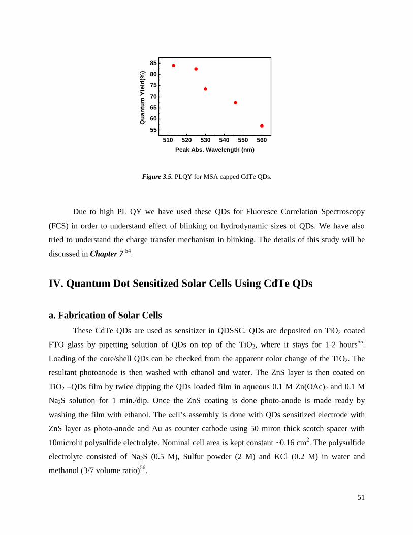
51
510 520 530 540 550 560
55
60
65
70
75
80
85
Qu
an
tum
Yie
ld(%
)
Peak Abs. Wavelength (nm)
Figure 3.5. PLQY for MSA capped CdTe QDs.
Due to high PL QY we have used these QDs for Fluoresce Correlation Spectroscopy
(FCS) in order to understand effect of blinking on hydrodynamic sizes of QDs. We have also
tried to understand the charge transfer mechanism in blinking. The details of this study will be
discussed in Chapter 7 54
.
IV. Quantum Dot Sensitized Solar Cells Using CdTe QDs
a. Fabrication of Solar Cells
These CdTe QDs are used as sensitizer in QDSSC. QDs are deposited on TiO2 coated
FTO glass by pipetting solution of QDs on top of the TiO2, where it stays for 1-2 hours55
.
Loading of the core/shell QDs can be checked from the apparent color change of the TiO2. The
resultant photoanode is then washed with ethanol and water. The ZnS layer is then coated on
TiO2 –QDs film by twice dipping the QDs loaded film in aqueous 0.1 M Zn(OAc)2 and 0.1 M
Na2S solution for 1 min./dip. Once the ZnS coating is done photo-anode is made ready by
washing the film with ethanol. The cell’s assembly is done with QDs sensitized electrode with
ZnS layer as photo-anode and Au as counter cathode using 50 miron thick scotch spacer with
10microlit polysulfide electrolyte. Nominal cell area is kept constant ~0.16 cm2. The polysulfide
electrolyte consisted of Na2S (0.5 M), Sulfur powder (2 M) and KCl (0.2 M) in water and
methanol (3/7 volume ratio)56
.
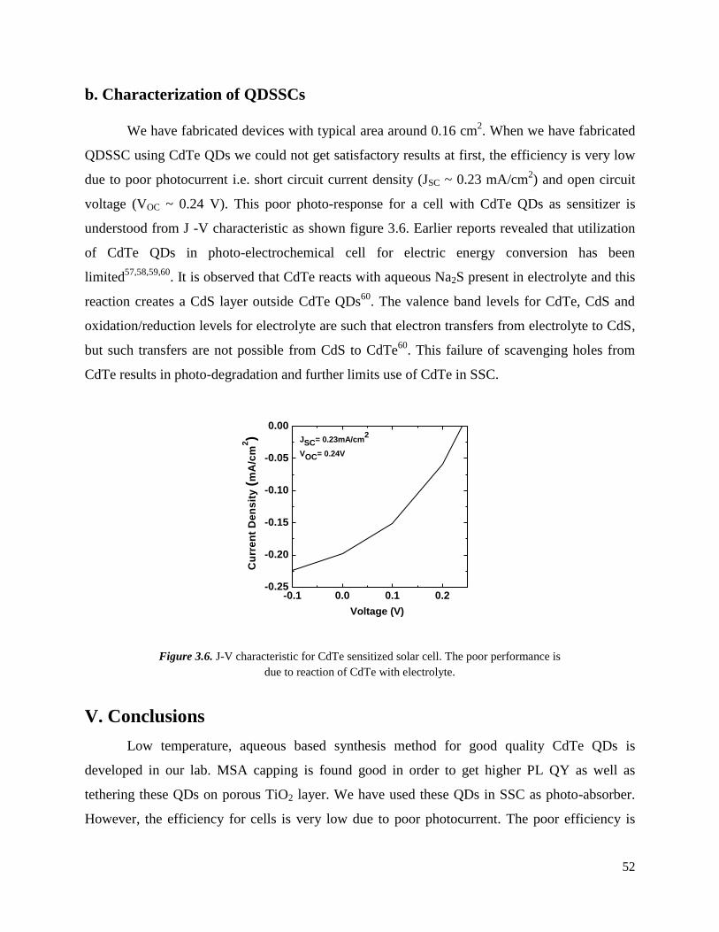
52
b. Characterization of QDSSCs
We have fabricated devices with typical area around 0.16 cm2. When we have fabricated
QDSSC using CdTe QDs we could not get satisfactory results at first, the efficiency is very low
due to poor photocurrent i.e. short circuit current density (JSC ~ 0.23 mA/cm2) and open circuit
voltage (VOC ~ 0.24 V). This poor photo-response for a cell with CdTe QDs as sensitizer is
understood from J -V characteristic as shown figure 3.6. Earlier reports revealed that utilization
of CdTe QDs in photo-electrochemical cell for electric energy conversion has been
limited57,58,59,60
. It is observed that CdTe reacts with aqueous Na2S present in electrolyte and this
reaction creates a CdS layer outside CdTe QDs60
. The valence band levels for CdTe, CdS and
oxidation/reduction levels for electrolyte are such that electron transfers from electrolyte to CdS,
but such transfers are not possible from CdS to CdTe60
. This failure of scavenging holes from
CdTe results in photo-degradation and further limits use of CdTe in SSC.
-0.1 0.0 0.1 0.2-0.25
-0.20
-0.15
-0.10
-0.05
0.00
Cu
rre
nt
De
ns
ity
(m
A/c
m2)
Voltage (V)
JSC= 0.23mA/cm2
VOC= 0.24V
Figure 3.6. J-V characteristic for CdTe sensitized solar cell. The poor performance is
due to reaction of CdTe with electrolyte.
V. Conclusions
Low temperature, aqueous based synthesis method for good quality CdTe QDs is
developed in our lab. MSA capping is found good in order to get higher PL QY as well as
tethering these QDs on porous TiO2 layer. We have used these QDs in SSC as photo-absorber.
However, the efficiency for cells is very low due to poor photocurrent. The poor efficiency is
53
mainly due to photo-degradation of CdTe in contact with electrolyte. This further creates
inability for scavenging holes from CdTe and thus performance degrades under exposure of
light. Due to excellent optical properties of the CdTe material as a photo-absorber we don’t
wanted to change the material. However, we tried to avoid the degradation and the inability of
hole scavenging using type-II heterostructure nanoparticle. The synthesis method for such
heterostructure and the improvement in cell performance will be discussed in next Chapter 4.

54
VI. References
1http://www.columbia.edu/cu/chemistry/fac-bios/brus/group/pdf-
files/semi_nano_website_2007.pdf Brus, L.E. (2007). "Chemistry and Physics of
Semiconductor Nanocrystals."
2 M. A. Reed, J. N. Randall, R. J. Aggarwal, R. J. Matyi, T. M. Moore and A. E. Wetsel,
Observation of discrete electronic states in a zero-dimensional semiconductor
nanostructure, Phys. Rev. Lett. 60 (6): 535–537, 1988.
3 L. Greenemeier, (5 February 2008). "New Electronics Promise Wireless at Warp Speed".
Scientific American.
4 E. Prati, M. De, B. Marco, C. Matteo, F. M. Simonei, D. Kotekar-Patil, M. Ruoff, K. Dieter
Few electron limit of n-type metal oxide semiconductor single electron
transistors. Nanotechnology 23 (21): 215204, 2012.
5 D. A. Jenny and R. H. Bube, Semiconducting CdTe, Phys. Rev. 96, 5, 1954.
6 B. Goldstein, Properties of PV Films of CdTe, Phys. Rev 109 (2), 601, 1958.
7 Y. A. Vodakov, G. A. Lomakina, G. P. Naumov and Y. P. Maslakovets, A P-N Junction
photocell made of CdTe, Soviet Physics, Solid State 2 (1), 1, 1960.
8 K. Zweibel, J. Mason, V. Fthenakis, A Solar Grand Plan, Scientific American, Jan 2008. CdTe
PV is the cheapest example of PV technologies. and prices are about 16¢/kWh with US
Southwest sunlight.
9 M. A. Green, Y. Emery, W. W. Hishikawa, E. D. Dunlop, Solar Efficiency Tables (version 42).
Progress in Photovoltaics: Research and Application 21: 827-837.
10 S. F. Wuister, I. Swart, F.van Driel, S. G. Hickey and C. de Mello Donega, Highly luminescent
water soluble CdTe quantum dots, Nanoletter, 3(4), 503-507, 2003.
11 G. Entine, D. A. Garcia, D. E. Tow, Review of CdTe medical applications, Rev. Phys. Appl.
12, 355, 1977.
12 N. P. Gaponik, D. V. Talapin, A. L. Rogach and A. Eychmuller, Electrochemical Synthesis of
CdTe Nanocrystal/Polypyrrole Composites for Optoelectronic Applications, J. Mater. Chem.,
10, 2163-2166, 2000.

55
13
M. Gao, C. Lesser, S. Kirstein, H. Mohwald, A. L. Rogach and H. J. Weller,
Electroluminscence of different colors from polycation/CdTe nanocrystal self-assembled films,
J. Appl. Phys. 87, 2297-2302, 2000.
14 C. Bertoni, D. Gallardo, S. Dunn, N. Gaponik and A. Eychmuller, Fabrication and
characterization of red-emitting electroluminescent devices based on thiol-stabilized
semiconductor nanocrystals, Appl. Phys. Lett. 90, 034107, 2007.
15 M. Gao, J. Sun, E. Dulkeith, N. Gaponik, U. Lemmer and J. Feldmann, Lateral pattering of
CdTe Nanocrystal films by electric field directed layer by layer assembly, Langmuir, 18, 4098-
4102, 2002.
16 D. V. Talapin, S. K. Poznyak, N. P. Gaponik, A. L. Rogach and A. Eychmuller, A. Synthesis
of surface modified colloidal semiconductor nanocrystals and study of photo-induced charge
separation and transport in nanocrystal-polymer composites, Physica E, 14, 237-241, 2002.
17 D. M. Guldi, I. Zilbermann, G. Anderson, N. A. Kotov, N. Tagmatarchis and M. Prato, J.
Mater. Chem., 15, 114, 2005.
18 Gary Hodes, Comparison of dye- and semiconductor-sensitized porous nanocrystalline liquid
junction solar cells, J. Phys. Chem. C,112, 17778–17787, 2008.
19 A. Kongkanand, K. Tvrdy, K. Takechi, M. Kuno and P. V. Kamat, Quantum dot solar cells.
Tuning photoresponse through size and shape control of CdSe-TiO2 architecture, J. Am.
Chem. Soc. 130, 4007−4015, 2008.
20 M. C. Beard, J. M. Luther, A. G. Midgett, O. E. Semonin, J. C. Johnson and A. J. Nozik, IEEE
Phot. Spec. Conf., 000370−000375, 2010.
21 I. Robel, M. Kuno and P. V. Kamat, Size-Dependent electron Injection from Excited CdSe
Quantum Dots into TiO2 Nanoparticles, J. Am. Chem. Soc., 129, 4136−4137, 2007.
22 Y. Yang, W. Rodriguez-Cordoba, X. Xiang and T. Q. Lian, Multiple exciton generation and
dissociation in PbS quantum dot-electron acceptor complexes, Nano Lett., 12, 303−309, 2012.
23 A. J. Nozik, M. C. Beard, J. M. Luther, M. Law, R. J. Ellingson and J. C. Johnson,
Semiconductor quantum dots and quantum dot arrays and applications of multiple exciton
generation to third generation photovoltaic solar cell, Chem. Rev., 110, 6873−6890, 2010.
56
24
Y. Keyou, C. Wei, and Y. Shihe, Significantly Enhanced Open Circuit Voltage and Fill Factor
of Quantum Dot Sensitized Solar Cells by Linker Seeding Chemical Bath Deposition, J. Phys.
Chem. C, 117, 92−99, 2013.
25 L. J. Diguna, Q. Shen, J. Kobayashi and T. Toyoda, High efficiency of CdSe quantum- dot-
sensitized TiO2 inverse opal solar cells, Appl. Phys. Lett., 91, 023116, 2007.
26 I. Robel, V. Subramanian, M. Kuno, P. V. Kamat, Quantum Dot solar cells. Harvesting light
energy with CdSe nanocrystals molecularly linked to mesoscopic TiO2 films, J. Am. Chem.
Soc.128, 2385−2393, 2006.
27 I. Mora-Sero, S. Gimenez, T. Moehl, F. Fabregat-Santiago, T. Lana-Villareal, R. Gomez and J.
Bisquert, Improving the performance of colloidal quantum-dot-sensitized solar
cells, Nanotechnology, 19, 424007, 2008.
28 Y. L. Lee and Y. S. Lo, Highly Efficient Quantum-Dot-Sensitized Solar Cell Based on Co-
Sensitization of CdS/CdSe, Adv. Funct. Mater., 19, 604−609, 2009.
29 H. Lee, H. C. Leventis, S. J. Moon, P. Chen, S. Ito, S. A. Haque, T. Torres, F. Nuesch, T.
Geiger, S. M. Zakeeruddin, M. Gratzel and M. K. Nazeeruddin, PbS and CdS quantum dot-
sensitized solid-state solar cells: "Old Concepts, New Results, Adv. Funct. Mater., 19,
2735−2742, 2009.
30 R. Plass, S. Pelet, J. Krueger, M. Gratzel and U. J. Bach, Quantum Dot sensitization of
organic-inorganic hybrid solar cells, Phys. Chem. B, 106, 7578−7580, 2002.
31 H. Lee, M. K. Wang, P. Chen, D. R. Gamelin, S. R. Zakeeruddin, M. Gratzel and M. K.
Nazeeruddin, Efficient CdSe quantum prepared by an improved successive ionic layer
adsorption and reaction process, Nano Lett., 9, 4221−4227, 2009.
32 J. R. Mann and D. F. Watson, Adsorption of CdSe Nanoparticles to Thiolated TiO2 Surfaces:
Influence of Intralayer Disulfide Formation on CdSe Surface Coverage, Langmuir, 23, 10924–
10928, 2007.
33 D. Pernik, K. Tvrdy, J. G. Radich and P. V. Kamat, Tracking the Adsorption and Electron
Injection Rates of CdSe Quantum Dots on TiO2: Linked Versus Direct Attachment, J. Phys.
Chem. C, 115, 13511–13519, 2011.

57
34
C. B. Murray, D. J. Norris and M. G. Bawendi, Synthesis and characterisation of nearly
monodisperse CdE (E= sulphur, selenium, tellurium) semiconductor nanocrystallites, J. Am.
Chem. Soc., 115, 8706-8715, 1993.
35 D. V. Talapin, A. L. Rogach, A. Kornowski, M. Haase, H. Weller, Highly Luminescent
Monodisperse CdSe and CdSe/ZnS Nanocrystals Synthesized in a Hexadecylamine –
Trioctylphosphine Oxide – Trioctylphospine Mixture, Nano Lett., 1, 207-211, 2001.
36 L. Qu, Z. A. Peng and X. Peng, Alternative Routes toward High Quality CdSe Nanocrystals
Nano Lett., 1, 333-337, 2001.
37 D. V. Talapin, A. L. Rogach, I. Mekis, S. Haubold, A. Kornowski, M. Haase and H. Welle,
Synthesis and Surface Modification of Amino-Stabilized CdSe, CdTe and InP Nanocrystals,
Colloids Surf. A, 202, 145-154, 2002.
38 H. Mattoussi, J. M. Mauro, E. R. Goldman, G. P. Anderson, V. C. Sundar, F. V. Mikulec and
M. G. Bawendi, Self-assembly of CdSe-ZnS quantum dots biaconjugates using an engineered
recombinant protein, J. Am. Chem. Soc., 122, 12142-12150, 2000.
39 D. Gerion, F. Pinaud, S. C. Williams, W. J. Parak, D. Zanchet, S. Weiss, and A. P. Alivisatos,
Synthesis and properties of biocompatible water-soluble silica-coated CdSe/ZnS
semiconductor quantum dots. J. Phys. Chem. B, 105, 8861-8871, 2001.
40 B. Dubertret, P. Skourides, D. J. Norris, V. Noireaux, A. H. Brivanlou and A. Libchaber, In
vivo imaging of quantum dots encapsulated in phospholipid micelles. Science, 298, 1759-1762,
2002.
41 I. Sondi, O. Siiman, S. Koester and E. Matijevic, Preparation of aminodextran
CdSnanoparticle complexes and biologically antibodyaminodextran –CdS nanoparticles
conjugates, Langmuir, 16, 3107-3118, 2000.
42 J. O. Winter, T. Y. Liu, B. A. Korgel and C. E. Schmidt, Recognition Molecule Directed
Interfacing Between Semiconductor Quantum Dots and Nerve Cells, Adv. Mater., 13, 1673-
1677, 2001.
43 Kiran P. Kadlag, Padmashri Patil, M. Jagadeeswara Rao, Shouvik Datta, Angshuman Nag,
Luminescence and Solar Cell from Ligand-Free Colloidal AgInS2 Nanocrystals, Cryst. Eng.
Comm, 16, 3605-3612, 2014.

58
44
A. L. Rogach, T. F., T. A. Klar, J. F., N. Gaponik, V. Lesnyak, A. Shavel, A. Eychmuller, Y.
P. Rakovich, and J. F. Donegan, Aqueous Synthesis of Thiol-Capped CdTe Nanocrystals:
State-of-the-Art, J. Phys. Chem. C, 111, 14628-14637, 2007.
45 M. Gao, S. Kirstein, H. Mohwald, A. L. Rogach, A. Kornowski, A. Eychmuller and H. Weller,
Electroluminescence of Different Colors from Polycation/CdTe Nanocrystal Self-Assembled
Films, J. Phys. Chem. B, 102, 8360, 1998.
46 N. Gaponik, D. V. Talapin, A. L. Rogach, K. Hoppe, E. V. Shevchenko, A. Kornowski, A.
Eychmuller and H. Weller, Thiol-capping of CdTe nanocrystals: an alternative to
organometallic synthetic routes, J. Phys. Chem. B, 106, 7177, 2002.
47 A. L. Rogach, L. Katsikas, A. Kornowski, D. Su, A. Eychmuller, H. Weller and H. Ber.
Bunsen-Ges. Synthesis and Characterization of Thiol-Stabilized CdTe Nanocrystals, Phys.
Chem. 100, 1772, 1996.
48 H. Zhang, Z. Zhou, B. Yang and M. J. Gao, Vesicles with superior stability at high
temperature, Phys. Chem. B, 107, 8, 2003.
49 L. Li, H. F. Qian, N. H. Fang and J. C. Ren, Significant enhancement of the quantum yield of
cdte nanocrystals synthesized in aqueous phase by controlling the pH and concentrations of
precursor solutions. Lumin., 116, 59–66, 2006.
50 E. Ying, D. Li, S. Guo, S. Dong and J. Wang, Synthesis and Bio-Imaging Application of
Highly Luminescent Mercaptosuccinic Acid-Coated CdTe Nanocrystals. PLoS ONE 3(5):
e2222. doi:10.1371/journal.pone.0002222, 2008.
51 R. J. Bandaranayake, G. W. Wen, J. Y. Lin, H. X. Jiang, and C. M. Sorensen, Structural phase
behavior in II–VI semiconductor nanoparticles, Appl. Phys. Lett. 67, 831, 1995.
52 J. R. Lakowicz, Principles of Fluorescence Spectroscopy, 2nd Ed., Kluwer Academic, New
York, 1999.
53 M. Gao, S. Kirstein, H. Mohwald, A. L. Rogach and A. Kornowski, Strongly
photoluminescent CdTe nnanocrystals by proper surface modification. J. Phys. Chem. B, 102,
8360–8363, 1998.
54 A.V.R. Murthy, Padmashri Patil, Shouvik Datta, Shivprasad Patil, Photoinduced dark fraction
due to blinking and photodarkening probability in aqueous CdTe quantum dots. J. Phys. Chem.
C. 117, 13268-75, 2013.

59
55
Z. Pan, H. Zhang, K. Cheng, Y. Hou, J. Hua, and X. Zhong, Highly efficient inverted type-I
CdS/CdSe core/shell structure QD-sensitized solar cells, ACS Nano, 6, 3982, 2012.
56 Y.-L. Lee and C.-H. Chang, Efficient polysulfide electrolyte for CdS ... solar cells, J. Power
Sources, 185, 584, 2008.
57 S. M. McGregor, I. M. Dharmadasa, I. Wadsworth and C. M. Care, Growth of CdS and CdTe
by Electrochemical Technique for Utilization in Thin Film Solar Cells. Opt. Mater. 6, 75–82,
1996.
58 A. Kampmann and D. Lincot, Photoelectrochemical Study of Thin Film Semiconductor
Heterostructures: Junction Formation Processes in CdS/CdTe Solar Cells. J. Electroanal Chem.
418, 73–81, 1996.
59 Mathew, X.; Bansal, A.; Turner, J. A.; Dhere, R.; Mathews, N. R.; Sebastian, P. J.
Photoelectrochemical Characterization of Surface Modified CdTe for Hydrogen Production. J.
New Mater. Electrochem. Syst. 5, 149–154, 2002.
60 J. H. Bang and P. V. Kamat, Quantum Dot Sensitized Solar Cells. A Tale of Two
Semiconductor Nanocrystals: CdSe and CdTe, ACS NANO, 3 (6), 1467–1476, 2009.

60

61
Chapter 4
Aqueous Synthesis of CdTe/CdSe Core/Shell Quantum
Dots and their Application in Sensitized Solar Cell
I. Introduction
Currently world is facing a huge energy crisis and demand will continue to increase by
many folds in the near future. We have also seen that dependence on non-renewable energy
sources cannot give us a permanent solution as these sources are exhaustible and often produce
non-repairable damage to earth‟s environment. So a more promising way to satisfy such huge
energy demands without creating pollution is use of renewable energy sources like sunlight
through solar cells. Great efforts have been made to make affordable solar cells so that power
can be generated at a cost lower than the cost of traditional electricity generation. A third
generation solar cell is considered very promising for increasing efficiency and making the
production processes affordable. Though the measured efficiency for these devices is low
compare to the first generation solar cells it can be used for niche applications such as charging
battery in the mobile phones, running small toys and watches etc. As these devices has less
operational lifetime and doesn‟t require high power conversion efficiency, solar cells with
somewhat reasonable efficiency of even 5-10% made at a lower manufacturing cost can be used
to reduce overall cost of these applications. Sensitized solar cells (SSC) are a class of third

62
generation cells which cost ~1/3rd
to 1/5th
of the other semiconductor solar cells based crystalline
materials and or vapor deposited thin films. The comparatively lesser cost is mainly due to lower
material utilization rate in third generation solar cells. A lot of research is being done in this field
since the first sensitized solar cell report is published1. The importance of QDs in this regard is
also discussed in Chapter 3. There we have seen the method to synthesize CdTe QDs in aqueous
medium at low temperature. The problem of self-destruction of CdTe QDs in contact with
electrolyte and as a result, a non-efficient sensitized solar cell is also discussed in Chapter 3.
According to literature, use of doped QDs2,3
, co-sensitization4,5,6
and core/shell heterostructure
QDs7,8,9,10
enables better power conversion efficiency compared to use of single QDs. This may
be due to limitation of absorption range of single QDs as well as stability issues related to
particular QDs11,12,13,14,15
.
Core/shell (CS) heterostructure QDs of II-VI semiconductors have found a wide range of
applications in optoelectronics16,17
, bio-imaging18
and photovoltaics19,20,21
etc. CdTe/CdSe is one
such type-II heterostructure CS material. In type-II heterostructures, the core and shell are made
up of two different semiconducting materials with a particular valence and conduction band
alignment at the hetero-interface as shown in figure 4.1a Figure 4.1b shows schematic for
core/shell hetrostructure which clearly differentiates the core, shell and capping layer material.
Figure 4.1. Schematic describing a) band alignment in type-II heterostructure and b)
core, shell and capping layer (micelles like structure after CdSe) together forming
core/shell heterostructure.
The band alignment of these semiconductor QDs is such that it efficiently assists the all
important charge separation of photo-excited electron hole pairs22,23,24
. This charge separation

63
process effectively slows down the radiative recombination rates of photo-generated carriers,
which allows better harvest of photo-generated electron-hole pairs in photovoltaic cells19,25
and
also in photoconductive devices19
. Therefore, lot of attention has been focused on the
synthesis25,26,27,28
of these core/shell QDs
as well as on their use in nano-photovoltaics.
There are many reports on synthesis of different type-II hetero-structures like
CdSe/ZnTe29,30,31
, CdTe/CdSe27,32,33,34,35
, CdTe/CdSe alloys36
, CdSe/CdS26,37,38,39
etc. using a
variety of complex wet chemical methods involving elaborate purification techniques. There are
also reports18,2827,28
which explain the mechanism of charge transfer in CS QDs as a function of
shell thickness but most of these have been synthesized using hazardous chemicals and at high
temperatures of >250 ˚C but to the best of our knowledge, there is only one report8 using these
QDs for solar cells ( ~ 2.4%). Moreover, the effect of varying shell thickness on solar cell
performance is not well studied.
In this chapter we report the investigations of a simple aqueous synthesis of CdTe/CdSe
based CS heterostructure QDs grown without any seed purification at considerably lower
temperature of 80 ˚C. These materials reveal good structural, optical quality as well as
comparatively similar power conversion efficiency of ~2% for such material system. A quicker
and procedurally simpler chemical synthesis route is always economically desirable for large
scale production of these heterostructure QDs. The low temperature aqueous synthesis technique
without seed purification presented here provides one such simple and economic processing
method to grow good quality of CdTe/CdSe core shell QDs for mass production. We have also
demonstrated that the solar cell parameters of these sensitized cells are strong functions of the
shell thickness as expected for such charge separating type-II heterostructures. The schematic
diagram showing CdTe/CdSe adsorbed on TiO2 along with ZnS layer and charge transfer process
between them is given as figure 4.2. The assembly of QDs on TiO2 is another important factor
which affects the performance of SSC. The MSA capping ligand here works as a bi-linker
molecule whose one end is connected to QDs and other end helps in tethering QDs on TiO2.
In general these bi-linker molecules are insulating in nature. So their presence in
between QDs and TiO2 degrade the charge transport and hence affect the short circuit current
density (JSC). The sintering of photoanode is known for removal of such bi-linker
molecules10,33,40,41,42
. The effect of sintering sensitized photoanode at different temperature for
improvement of JSC is also presented in this chapter.

64
Figure 4.2. Schematic diagram describing the charge separation and charge transfer
processes in CdTe/CdSe based sensitized solar cell. The system consists of
CdTe/CdSe CS QDs adsorbed on TiO2 electrode and then coated with a thin ZnS
layer. Here, electron hole pair is photo generated in CdTe and these electrons are
transferred to TiO2 via CdSe and are then collected at FTO contact. The electron from
electrolyte probably tunnels to neutralize the vacancy to complete the photo
electrochemical cycle.
II. Experimental Methods
a. Chemicals Used For Synthesis
All chemicals utilized in this study are used as purchased without any further purification
or treatments. Cadmium chloride, sodium borohydride, mercapto-succinic acid and boric acid,
acetic acid, sodium sulfide, sulfur powder, titanium tetrachloride, and potassium chloride are
purchased from Merck. Sodium tellurite and sodium selenite are purchased from Loba Chemie.
Trisodium citrate is purchased from Thomas Baker. Terpineol, ethyl cellulose, rhodamine-6g are
purchased from Sigma Aldrich F:SnO2 (FTO) coated glass is purchased from Solaronix (8
ohm/square). Degussa P-25 TiO2 nanoparticles are a generous gift from Evonik. Ethanol and
methanol are HPLC grade. De-ionized (D. I.) water with 18 MΩ-cm is used.
b. Synthesis of CdTe Core QDs (i.e. Seed Solution)
CdTe QDs are synthesized using the procedure developed in our lab43
and as discussed in
Chapter 3. Reaction is carried out in a three neck flask, where first neck is used for water
condensation; second one for monitoring temperature and third one take out aliquots. Reactions

65
proceeded in buffer solutions of boric acid and trisodium citrate, where 15 mM of boric acid and
15 mM of trisodium citrate are used in 50 ml de-ionized water to make a buffer solution of pH-8.
Precursor solution for CdTe QDs are made with cadmium chloride (1 mM), sodium tellurite
Na2TeO3 (0.25 mM), and mercapto-succinic acid (MSA) (3 mM) in 50 ml of buffer solution of
pH-8 at 25 ˚C. After vigorous stirring (~900 rpm) of precursors for 5 minutes, 20 mg of sodium
borohydride (NaBH4) is added into the solution. This reaction is carried out for 10 minutes inside
the flask. After that flask is attached to the condenser and then heated along with stirring at 80˚C
under ambient condition. Aliquots are collected at different time intervals after starting the
reaction and are characterized further. We used these CdTe QDs as seeds with and without
purification for further synthesis of CdTe/CdSe CS QDs heterostructure. Structural and optical
properties for CS QDs with and without purification are studied and discussed below in detail.
c. Synthesis of CdTe/CdSe core/shell heterostructure QDs
c. 1. With Purification of Seed Solution
Traditional CS synthesis processes consist of rigorous purification of CdTe seed
QDs25,44
. In this method, we stop the reaction after attaining certain peak wavelength of
excitonic absorbance of these CdTe QDs (here in this case absorbance peak ~507 nm). We have
purified CdTe QDs which involves precipitation of QDs with ethanol and washing four times
using a centrifuge (~6000-7000 rpm). We assume that there is not much loss of CdTe QDs
while washing. These purified CdTe QDs are subsequently dispersed into 43 ml of buffer
solution of pH 8 and subsequently heated to 80 ˚C along with stirring of ~900 rpm. To make top
CdSe shell layer on CdTe core, we have mixed 0.001 M sodium selenite precursor and 0.02 g of
NaBH4 in 7 ml deionized water and at last we have added it to the hot purified solution of seed
CdTe QDs. Finally after 10 minutes into the reaction, we have enriched the solution with Cd2+
ions by adding 0.5 mM CdCl2 and 1.5 mM MSA. Four such aliquots are collected at different
time intervals which then used for further characterization and compared with CS QDs
synthesized without purification of seeds. These samples are labeled as CdTe, CS1, CS2, CS3
and CS4 (Core QDs used as seeds are labeled as CdTe). Note that CS QDs has nearly same
absorption maximum wavelength to that of CS QDs synthesized without purification of seeds.

66
However, we have not labeled these CS QDs by their absorption maximum just to avoid
confusion.
c. 2. Synthesis of CdTe/CdSe CS QDs Without Purification of Seed Solution
In this procedure we have not purified the seed CdTe QDs. Here we allow CdTe QDs to
increase until the QDs absorbance matched with desired wavelength; the size of the QD is
correlated to the absorbance of QDs. Once we get the desired absorbance wavelength, we have
added 1 mM sodium selenite precursor in as prepared seed CdTe QDs solution at 80 ˚C.
Thereafter, we have enriched this solution with Cd2+
ions by adding 0.5 mM cadmium chloride.
CdSe is then allowed to grow on the CdTe QDs with heating at 80 ˚C and continuous stirring of
~900 rpm. Aliquots are collected at different time intervals from the three neck flask and used for
further characterization. Four representative CdTe/CdSe core/shell QDs are selected and its
optical as well as structural properties are studied and compared with that of CS QDs synthesized
after purification of core QDs. The QDs are labeled with its absorption maximum wavelength as
QD534, QD568, QD592 and QD606. The same set of CS QDs is used as sensitizer for the fabrication
of sensitized solar cell.
d. Fabrication of Sensitized Solar Cells
The FTO coated glass electrodes are cleaned as discussed in Chapter 3 section II-D,
using diluted soap solution, water and ethanol and finally heated at 450 ˚C for 10 mins in order
to remove contaminants. P25 TiO2, acetic acid, terpineol, ethyl cellulose, water and ethanol are
used to prepare TiO2 paste; detailed procedure is given in Chapter 3 section II-C (The exact
procedure followed for preparation is also given here45
).
Even though QDs are of high quality and stable for long time, it is still a great challenge
to assemble uniform layer of previously synthesized QDs on mesoporous TiO2 with high area
coverage. In order to improve the material loading and surface covering we have used freshly
prepared MSA capped aqueous QDs. The as prepared QDs suspension (with absorbance „2‟ at
first excitonic absorption peak) was pipetted directly on TiO2 electrode where it is allowed to
stay for two hours10,36
. QDs loaded TiO2 are then washed using ethanol and water. The loading
of core/shell QDs can be checked from the coloring of TiO2. The ZnS layer is then coated on
TiO2–QDs film by twice dipping the QDs loaded film in aqueous 0.1 M Zn(OAc)2 and 0.1 M

67
Na2S solution for 1 min./dip. Once the ZnS coating is done, photo-anode is made ready by
washing the film with ethanol and sintering it at ~200 ˚C, ~400 ˚C in ambient for 5 mins.
Finally, the cells are prepared by assembling QDs sensitized electrode with ZnS layer as
photo-anode and Au as counter cathode using 50 μm thick scotch spacer with 10 microlit
polysulfide electrolyte. The polysulfide electrolyte consists of Na2S (0.5 M), Sulfur powder (2
M) and KCl (0.2 M) in water and methanol (3/7 volume ratio)46
. Several such cells are made and
one with best efficiency is chosen as final data. Nominal cell area is kept constant ~0.16 cm2.
III. Results and Discussions
a. Structural and Optical Properties
In this section we will discuss both structural and optical qualities of these CS
heterostructure QDs using X-ray diffraction (XRD) spectroscopy, optical absorption
spectroscopy, steady state photoluminescence spectroscopy and finally by TCSPC. Some of
these optical spectroscopy results for CdTe/CdSe CS QDs are described in Table #4.1. Figure 4.3
shows the evolution of XRD spectra for core/shell QDs synthesized without purification of
seeds.
Figure 4.3. Evolution of core/shell crystal structure for CdTe/CdSe synthesized using
unpurified core QDs is shown using XRD pattern. The planes for CdTe and CdSe are
given for reference.

68
Here the CdTe QDs are the core QDs used as seeds for forming core/shell structure and rest of
the samples are CS structures after consecutive growth of shell layer. The representative X-Ray
diffraction peak positions corresponding to bulk CdTe and bulk CdSe materials are shown at the
bottom and top of the figure for reference47
. The XRD spectra of CdTe QDs shows peaks with d-
values that corresponding to (111), (220) and (311) planes of the cubic phase of CdTe47
(aCdTe=
0.648 nm44
). We noticed that XRD peaks shift to higher angles as compared to that of only CdTe
QDs as soon as CdSe shell forms on these CdTe seeds and finally matches with the generic CdSe
peaks. The (311) peaks start appearing at 51˚ after shell growth which is not visible in only
CdTe. Moreover, we identify these dominant XRD peaks of CS QDs mostly with (111), (220),
(311) planes of cubic crystallites of CdSe47
(aCdSe = 0.605 nm) thus confirming the formation of
top shell layer. This reaffirms the formation of CdSe shell layer on top of CdTe core. Moreover,
nearly similar spectral features of XRD are observed for CS QDs synthesized with purified seed
QDs as given in figure 4.4. From figure 4.3 and figure 4.4 it is clear that similar shift occur in the
planes features corresponding to (111) and (220) to higher angles instead of showing two
independent peaks. This supports our argument that it cannot be a mixture of two differently
grown QDs33
. This gradual shifting of peak to higher angle also indicates presence of strain at
the interface due to lattice mismatch of CdTe and CdSe QDs44
.
Figure 4.4. XRD spectra for CdTe and CdTe/CdSe CS NCs synthesized using
unpurified and purified seed NCs.

69
The morphology of seed CdTe and QD606 CS QDs synthesized using unpurified core is
studied using HR-TEM and images are given as figure 4.5 and 4.6 respectively. The image
clearly shows that CdTe QDs are nearly spherical. Magnified HRTEM image of representative
QD sample is given as left inset for both of the samples.
Figure 4.5. Structural characterization for MSA capped CdTe QDs using HRTEM.
The measured median diameter of CdTe QDs is ~2.3 nm.
Figure 4.6. HRTEM image for thickest shell CdTe/CdSe CS QDs synthesized using
unpurified core QDs i.e. QD606 sample. By scrutinizing high-resolution TEM, the
lattice fringe of CdTe (111) is clearly reflected.
Diameters of QDs are first analyzed using „ImageJ‟ software. This procedure is repeated and
values are averaged to minimize the error. The average QDs diameter is assessed via this
statistical analysis of measured HRTEM images of these QDs. The final histogram of percentage
of such QDs having a particular size range is shown as right inset for both the samples in figure
4.5 and 4.6. The median diameter of CdTe QDs is estimated from the HRTEM image and it is

70
found to be ~2.3 nm. Similarly, the HRTEM image CdTe/CdSe core–shell structures also shows
nearly spherical shape. The median particle size (~ 4 nm from the HRTEM images) is found to
be higher than that of CdTe seed QDs. By scrutinizing high-resolution TEM, the lattice fringe of
CdTe (111) is clearly reflected as shown in left inset of figure 4.6. From both HRTEM images, it
can be concluded that the QD diameter increases by about 2 nm upon shell growth. Interestingly,
the smallest such CS QDs diameter for QD606 is ~3.6 nm. We could not find any CS QDs smaller
than this minimum size from the statistical analysis of about fifty CS QDs scanned during the
imaging process. This actually means CdSe is growing as shell layer on CdTe seed QDs and not
growing separately as independent crystals.
The evolution of optical absorption spectra of CdTe/CdSe CS QDs synthesized without
purification of seed QDs is shown in figure 4.7. Here aliquots are taken at different time intervals
during the growth of shell layer. The absorption spectra for CdTe/CdSe CS QDs synthesized
using purified seed is also given for comparison as figure 4.8. Here in both figure 4.7 and figure
4.8 the spectrum with lowest absorption wavelength is the spectrum for core QDs which is used
as seed QDs. Rest of the samples has CdSe shell layers growing on top of respective CdTe seeds.
400 500 600 700
400 500 600 700
Ab
sorb
an
ce (
a.u
.)
Wavelength (nm)
CdTe
QD534
QD568
QD592
QD606
Figure 4.7. Absorption spectra for CdTe/CdSe CS QDs synthesized without purifying
CdTe seed particles. Magnified spectra are given as insets for better insight of the red
shifts of the excitonic absorption peaks.
A preliminary growth of the CdSe shell layer actually red shifts the absorption peak in both
cases. This behavior continues and further growth of CdSe shell layer gradually shifts these
excitonic peaks to higher and higher wavelength. Moreover, there is a growing presence of a

71
shoulder like feature as shown in figure 4.7 and 4.8 which is totally absent in MSA capped CdTe
seed QDs (Please refer Chapter 3 figure 3.3). Additionally, we also observe that the shoulder
like absorption edge becomes prominent in thickest CdSe shell layer samples. So this shoulder
like second absorption feature can certainly be assigned to the direct optical absorption in the
CdSe shell layer only48
. However, this red shift of excitonic peak and CdSe shoulder are present
in both CS QDs synthesized using both purified and unpurified seeds.
Figure 4.8. Absorption spectra for CdTe/CdSe CS QDs synthesized after purification
of seed QDs. Inset 1 is given for better insight of the red shifts of the excitonic
absorption peaks and inset 2 shows change in wavelength of excitonic peak of QDs
with refluxing time.
The evolution of optical spectra for only CdTe is also studied for comparison (Chapter 3,
figure 3.3). Interestingly, while experimenting, we observed that the CdTe growth (red shift in
absorption spectra) takes ~ 9 hours for getting absorption peak shifts from 456 nm to 565 nm in
contrast to that CS QDs synthesized by both ways takes only one and half hour time for getting
nearly same shift (for core/shell QDs the refluxing time is counted after addition of sodium
borohydride in the aqueous solution of reagents as mentioned in synthesis section. In case of
CdTe/CdSe CS QDs synthesized by using purified seeds the reflux time is calculated without
considering the purification interval). The plot for reflux time and the absorption red shift is
given as inset (2) of figure 4.8. Here, in case of CdTe, the significant red shift of optical
absorption spectra is due to slow increase in size of QDs with time as a result of Ostwald‟s
ripening effect. It is easy to understand that with increasing heating time, size of the CdTe QDs
increases which subsequently decreases its band gap due to the relaxation of size confinement of

72
charge carriers and thereby causing the redshift. Similarly one can also understand red shift of
the shoulder like feature (figure 4.7 and 4.8) representing the CdSe band edge with increasing
CdSe shell thickness as time passes. However, the reason for getting such relatively quicker red
shift with increasing refluxing time during formation of CdSe shell is not very well understood
although it is well known that reaction towards the formation of both only CdTe and only CdSe
proceed with similar rate. Moreover, not much difference in the optical absorption spectra is
observed for CdTe/CdSe CS QDs synthesized using purified and unpurified seeds. This also
reasserts why the redshift in unpurified CS QDs cannot come from any further growth of only
CdTe material, as qualitatively similar red shift is also observed in CS QDs synthesized using
purified seeds i.e. even in absence of any tellurium reagents and other byproducts from the CdTe
seed synthesis. This sizable difference between growths of only CdTe seed QDs with respect to
those CS QDs may explain the striking similarity in physical properties of CdTe/CdSe CS QDs
grown with and without purification. It is possible that the amount of Te2-
precursor is already
depleted while forming seed CdTe QDs for nearly one hour of heating and not oxidized.
Therefore, any further quicker growth of these unpurified CdTe seeds can be governed mainly by
the presence of additional Se2-
(as Se2-
are available in excess quantity as compared to that of
depleted Te2-
) in the reactant solution.
The PL spectra of these CdTe/CdSe CS QDs synthesized by both methods are studied
and given as figure 4.9 and 4.10.
500 600 700
CdTe
QD534
QD568
QD592
QD606
CdTe/CdSe; CdTe unpurified
No
rma
lize
d I
nte
ns
ity
Wavelength(nm)
Figure 4.9. PL spectra for CdTe/CdSe CS QDs synthesized without purification of
seeds.

73
Figure 4.10. PL spectra for CdTe/CdSe QDs synthesized after purification of seeds.
The ability of these QDs to cover long range wavelength is clearly visible from these
spectra. The quantitative similarities between the red shift of both ways synthesized QDs
importantly emphasizes the similarity in optical properties of these methods.
PL Quantum Yield (QY) is calculated for these CS QDs synthesized by using both
methods. For calculating PL quantum yield (QY) all samples are excited at 520nm. The resultant
PL peak intensities are further used to calculate QY for CdTe/CdSe CS QDs synthesized by both
procedures using the formula given in Chapter 2, section II. Figure 4.11 shows QY plots for
CdTe/CdSe CS QDs synthesized by both procedures.
Figure 4.11. PL QY for CdTe seed QDs and CdTe/CdSe CS QDs synthesized by both
procedures are plotted with respect to wavelength of excitonic absorption.
We want to emphasize that these estimates of PL QY (maximum QY ~60%) of
CdTe/CdSe CS QDs are as good as or even better than any such CS QDs made by using aqueous

74
routes27
.The wavelength on X axis corresponds to peak excitonic absorption wavelength for CS
QDs (from figure 4.7 and figure 4.8). We observe that the maximum quantum yield of
CdTe/CdSe CS QDs is ~60% for QD534 and also for CS2, for thickest shell QDs in both varieties
of CS QDs it further decreases to ~15%. This is possibly explained by the expected type-II band
alignment at CdTe/CdSe core-shell hetero-interface. The main reason for observed decrease in
PL QY with thicker shells might be that after photo-absorption one of the charge carriers (say
hole) is confined to core and other (say electron) is transferred to shell. So probability for these
delocalized charge carriers (either electrons or holes) to be trapped by non-radiative surface
states at the CS heterostructure interface is high. This can certainly lead to non-radiative re-
combinations49
which ultimately reduces the PL QY of these type-II band gap heterostructures.
Large lattice mismatch (~7%) and strain between core (CdTe) and shell (CdSe) layers can create
such non-radiative channels at the heterojunction interface of CS and thereby reduce PL
efficiency of core-shell materials26,44
. Most interestingly this variation of PL QY is almost
similar in CdTe/CdSe CS QDs prepared by both procedures. This again emphasizes that both
varieties of CS QDs are qualitatively similar with respect to optical absorption, type-II charge
separation and final PL QY.
In order to understand reasons for decrease in PL QY with increasing CdSe shell
thickness, we have studied PL lifetime of photoluminescence using TCSPC for CdTe/CdSe CS
QDs synthesized by both procedures as well as for CdTe seed QDs. The result for CS QDs
synthesized using unpurified core QDs is shown in figure 4.12. Photoluminescence decays are
measured using time correlated single photon counting (TCSPC) setup from Horiba Jobin Yvon
IBH, USA. As a pulse excitation source we have used 405 nm photo-excitation source from IBH,
UK (NanoLED-405L). The photoluminescence decay for CS QDs is tail-fitted using a double-
exponential decay function given by equation 4.1,
I (t) = a1 exp(-t/ 1)+ a2 exp(-t/ 2) (4.1)
Plots are fitted such that reduced chi-squared parameter (χ2) approaching 1 and resulting small
residual. Here, τ1 and τ2 are the photoluminescence decay constants obtained from above data
analysis and a1 and a2 are the corresponding pre-exponential factors. The average lifetime τavg is
calculated as an intensity-weighted sum of the two lifetime components. The obtained values of

75
τ1, τ2 and calculated average lifetime τavg for CS QDs synthesized with unpurified core QDs are
given in Table 4.1.
10 20 30 40 5010
100
1k
QD606
QD592
QD568
QD534
CP
S
Time (nS)
Figure 4.12. TCSPC results for CS QDs synthesized using unpurified core QDs.
Straight lines are the fit to all these curves.
Table 4.1. The chart summarizes emission wavelength and luminescence lifetime as a function
of shell thickness for CdTe/CdSe CS QDs synthesized without purification CdTe seed QDs.
TCSPC data of CS QDs are fitted with equation 4.1.
Sample
λ emission
(nm)
Quantum
Yield (%)
τ1
(ns)
τ2
(ns)
a1
(%)
a2
(%) τavg
(ns)
QD532 561 61 7.2 26 30 70 20.3
QD568 598 35 6.9 31 11 89 28.3
QD592 630 31 5.9 39.2 10 90 35.8
QD606 640 19 4.8 43.6 10 90 39.7
It is noticeable from figure 4.14 and Table 4.1 that average lifetime is a function of shell
growth as it is increases with CdSe shell thickness. The thinnest shell (QD532) has average
lifetime of ~20 ns which has been increased to ~39.7 ns for QD606. This type of change in
lifetime is absent in case of only CdTe (as shown in figure 4.13). This shows that type-II band
alignment of CdTe/CdSe core shell structure is actually driving the charge separation process

76
and thus providing additional active pathways for non-radiative recombination which is
competing with radiative luminescence. Such dependence of PL lifetime on shell thickness can
only take place when the rate of any additional non-radiative charge trapping process is affected
by electron delocalization in the type-II shell layer. Moreover, this happens when non-radiative
trapping rates become comparable to the type-II radiative processes and thereby selectively
consume a section of photo-excited charge carriers. Such long average lifetime also implies that
there are non-radiative decay channels which dominated over radiative decay channels in CS
QDs having thicker CdSe shells. This may evidently hinder the CS QDs from achieving high QY
(figure 4.11).
Figure 4.13. TCSPC results showing lifetime of charge carriers in case of CdTe QDs.
Comparatively there is no change in lifetime.
10 20 30 40 500
1k
2k
3k
4k
5k
CP
S
Time (nS)
CdTe/CdSe; CdTe purified
CS 1
CS 2
CS 3
CS 4
Figure 4.14. TCSPC results for CdTe/CdSe CS QDs synthesised with purified core
QDs.

77
Furthermore, qualitatively similar dependence of PL lifetime on shell thickness is observed in CS
QDs synthesized using purified core QDs. The decays spectra for CdTe/CdSe CS QDs
synthesized using purified core are given as fig 4.14 for comparison. This similarity proves that
optical properties for both types of CS QDs are comparable.
b. Quantum Dot Sensitized Solar Cells Using CdTe/CdSe Core-Shell QDs
We have fabricated Quantum Dot Sensitized Solar cells (QDSSCs) with FTO/TiO2 along
with unpurified CdTe/CdSe CS QDs/ZnS as photo-anode and gold electrode as cathode along
with a polysulfide electrolyte in between the electrodes. Fig 4.1 shows a schematic describing the
charge separation and charge transfer processes in such type-II sensitized solar cells. Here
electron-hole pair is generated in CdTe/CdSe CS QDs after absorbing photons. These photo-
generated electrons get transferred from CdTe/CdSe CS QDs to mesoporous TiO2 layer and are
finally collected by the FTO contact. At the same time, photo-generated holes are scavenged by
the polysulfide based redox electrolyte which thereby regenerates the reduced QDs. The charge
separation and transfer to different electrodes via transparent conducting oxide and electrolyte is
a very important process. Trapping of charge carriers also causes a reduction in current density.
CdTe is known for a poor SSC efficiency due to inability of hole scavenging using polysulfide
electrolyte. On other hand, CdSe shows superior performance as it is more stable11
. Many more
studies have been done on alloy/heterostructure QDs with CdTe as main constitutent36
. It has
been shown that having alloyed formation improves chemical stability of these QDs due to
hardened lattice structure and decreased inter-diffusion36
of polysulfide inside CdTe. Likewise
here in this study we are using CdTe/CdSe CS QDs as sensitizer.
As we have seen in Chapter 3, loading of QDs on TiO2 coated electrode is found to be
one of the major challenges in SSC. Direct growth of QDs on TiO2 suffers from broad optical
absorption due to uncontrolled growth and hence low power conversion efficiency. On the other
hand post-synthesis assembly of pre-synthesized QDs shows improvement in efficiency. In case
of pre-synthesized QDs the capping ligands are generally bi-linker molecules, here it is MSA.
While assembling the pre-synthesized QDs the –SH group is attached to QDs and the terminal
carboxyl group of capped QDs can effectively bind the TiO2 surface. The efficient loading of
QDs on TiO2 is studied by varying loading time. We found that the efficient sensitization is
happened only after two hours of loading. Figure 4.15 shows the effect of core/shell QDs
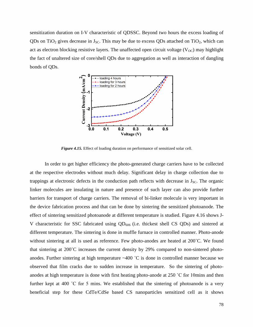
78
sensitization duration on I-V characteristic of QDSSC. Beyond two hours the excess loading of
QDs on TiO2 gives decrease in JSC. This may be due to excess QDs attached on TiO2, which can
act as electron blocking resistive layers. The unaffected open circuit voltage (VOC) may highlight
the fact of unaltered size of core/shell QDs due to aggregation as well as interaction of dangling
bonds of QDs.
Figure 4.15. Effect of loading duration on performance of sensitized solar cell.
In order to get higher efficiency the photo-generated charge carriers have to be collected
at the respective electrodes without much delay. Significant delay in charge collection due to
trappings at electronic defects in the conduction path reflects with decrease in JSC. The organic
linker molecules are insulating in nature and presence of such layer can also provide further
barriers for transport of charge carriers. The removal of bi-linker molecule is very important in
the device fabrication process and that can be done by sintering the sensitized photoanode. The
effect of sintering sensitized photoanode at different temperature is studied. Figure 4.16 shows J-
V characteristic for SSC fabricated using QD606 (i.e. thickest shell CS QDs) and sintered at
different temperature. The sintering is done in muffle furnace in controlled manner. Photo-anode
without sintering at all is used as reference. Few photo-anodes are heated at 200˚C. We found
that sintering at 200˚C increases the current density by 29% compared to non-sintered photo-
anodes. Further sintering at high temperature ~400 ˚C is done in controlled manner because we
observed that film cracks due to sudden increase in temperature. So the sintering of photo-
anodes at high temperature is done with first heating photo-anode at 250 ˚C for 10mins and then
further kept at 400 ˚C for 5 mins. We established that the sintering of photoanode is a very
beneficial step for these CdTe/CdSe based CS nanoparticles sensitized cell as it shows

79
improvement in the photocurrent. The measured current density is found to be increased
compared to the without sintered photo-anodes and photo-anodes sintered at 200 ˚C. However,
not much effect of sintering is observed on open circuit voltage (VOC). The parameters JSC, VOC
including efficiency (η) and fill factor (FF) for cells sintered at different temperature are given in
the table 4.2 for comparison. The only obvious reason for getting such high improvement in
current density is removal of bi-linker molecules through sintering. The sintering of sensitized
photo-anode at 400 ˚C is found to increase JSC by 102% and overall efficiency by 83% compared
to non-sintered photo-anodes.
Figure 4.16. Effect of sintering photoanode on JSC and efficiency.
Table 4.2. Effect of sintering temperature on the performance of solar cell is studied. Parameters
obtained from J-V characteristic in figure 4.16. Software from Science-tech is used in order to
extract values of FF.
Sintering
Temperature
JSC
mA/cm2
VOC
V
FF η
%
RT 4.4 0.52 0.47 1.08
200 ˚C 5.7 0.53 0.46 1.39
400 ˚C 8.9 0.53 0.42 1.98
As we have seen in Chapter 3, CdTe undergoes degradation due to reaction with polysulfide.
Here we will address the following question. Will the shell layer on CdTe help to improve the
efficiency of SSC as it tries to minimize the direct contact of electrolyte with CdTe? In this study

80
we used fixed core i.e. CdTe and effect of shell layer thickness i.e. CdSe on SSC performance is
studied. Samples with different shell thickness and so different absorption maximum wavelength
are like QD534, QD568, QD592 and QD606 used as sensitizer. Figure 4.17 shows I-V characteristic
for SSC fabricated using CdTe/CdSe CS QDs with different shell thickness after sintering at
400˚C. The observed values of short circuit current density (JSC), open circuit voltage (VOC) and
fill factor (FF) is given in table 4.3. In this experiment we did not find any change in VOC. But
much larger increment is observed in JSC and so in the efficiency of SSC. The systematic
increase in JSC is attributed to the extending light absorption range with increase in shell
thickness. The second possible reason might be the increased separation of CdTe/CdSe interface
from electrolyte. If the chemical instability of CdTe is affecting the current density and
efficiency, then the increased shell thickness might have succeeded in creating blocking layer in
between electrolyte and QDs. Therefore, higher the thickness, higher is the blocking/separation
of electrolyte and CdTe and so the higher current density and efficiency. Apart from
electrolyte/CdTe separation we also had the benefit of having type-II heterostructures, which
activates charge separation. Radiative recombination is a major problem in solar cell which
affects the current density. These type-II CdTe/CdSe core/shell hetero-structure spatially
separates charge carriers into two different materials (core and shell) which suppress radiative
recombination probability. This is also proved from QY measurement and life time data as
shown figure 4.11 and 4.12. As a result we found large ~300% increase in JSC in the QD with
thickest shell as compared to CS QDs having thinner shells.
Figure 4.17. J-V characteristic for SSC fabricated with different shell thickness
core/shell QDs.

81
Table 4.3. Parameters obtained from I-V characteristic given in figure 4.17. Here SSCs are
fabricated with CS QDs having different shell thickness. The effect of shell thickness on the JSC
and η is tabulated here.
Sample JSC
(mA/cm2)
VOC
V
FF η
%
QD534 2.2 0.52 0.35 0.4
QD568 5 0.53 0.45 1.19
QD592 8 0.53 0.44 1.86
QD606 8.9 0.53 0.42 1.98
The overall highest efficiency observed in these SSC with largest shell thickness is ~2%. This is
close to the value of 2.4% reported for SSC of similar material systems prepared using complex
synthesis routes at much higher synthesis temperatures. Comparable efficiency is also observed
for the sample having highest shell thickness in case of CdTe/CdSe core/shell QDs synthesized
using purified core i.e. CS4. Apart from having similarity in optical and structural properties,
both cells with purified and unpurified QDs also show comparable power conversion efficiency
which proves importance of this easy and quick synthesis method.
IV. Conclusions
Cost is one of the most important primary concerns of Solar Cell fabrication. Therefore,
any research in solar energy materials is important if it provides a better and economic way of
making good quality materials for solar cells having reasonable efficiency. Here we are reporting
a novel synthesis step which can reduce the overall time and cost of material synthesis as well as
solar cell fabrication. We have showed that aqueous wet chemical nanofabrication of charge
separating type-II CdTe/CdSe CS QDs at low enough temperature of ~ 80 ˚C using purified and
unpurified cores finally produce CS heterostructure QDs having good structural and optical
properties. We have also demonstrated that one can use such easy and quick synthesis of

82
CdTe/CdSe CS QDs without seed purifications to fabricate sensitized solar cells having power
conversion efficiency of ~2%. This nanofabrication strategy aims towards procedural
simplification of CS synthesis with additional benefit of high reproducibility. Longer PL
lifetimes observed in both cases of CS QDs with thicker shells implies that more non-radiative
decay channels are being added at the CS junction with increasing CdSe shell layer. This causes
a significant decrease in PL QY in CS QDs having thicker shells. Most interestingly,
luminescence decay rates of these CdTe/CdSe CS heterostructure QDs prepared by both
procedures are also nearly similar. This similarity again reflects on the importance and utility of
this economic route of using unpurified seeds in aqueous synthesis for mass production of such
technologically important CdTe/CdSe CS QDs for their application in optoelectronics and nano-
photovoltaic devices. We also found that the sintering of sensitized TiO2 photo-anode at high
temperature (~400 ˚C) is very important in order to remove insulating ligands and thereby
improve performance of the devices. The efficiency and short circuit current density is also
found to be a function of shell thickness as it is increases three fold with increase in shell
thickness.
83
V. References
1 B. O‟Regan, M. Gratzel, A low cost, high efficiency solar cell based on dye sensitized colloidal
TiO2 films, Nat. 335, 737-740, 1991.
2 P. K. Santra, P.V. Kamat, Mn-doped quantum dot sensitized solar cells: a strategy to boost
efficiency over 5%, J. Am. Chem. Soc. 134, 2508-2511, 2012.
3 J. Luo, H. Wei, Q. Huang, X. Hu, H. Zhao, R. Yu, D. Li, Y. Luo and Q. Meng, Highly
efficient core–shell CuInS2–Mn doped CdS quantum dot sensitized solar cells, Chem.
Commun., 49, 3881-3883, 2013.
4 Y.-L. Lee, Y.-S. Lo, Highly efficient quantum-dot-sensitized solar cell based on co-
sensitization of CdS/CdSe, Adv. Funct. Mater. 19, 604–609, 2009.
5 G. Zhu, L. Pan, T. Xu, Z. Sun, CdS/CdSe-Cosensitized TiO2 photoanode for quantum-dot-
sensitized solar cells by a microwave-assisted chemical bath deposition method, ACS Appl.
Mater. and Interface 3, 3146-3151, 2011.
6 J. Tian, R. Gao, Q. Zhang , S. Zhang , Y. Li , J. Lan , X.i Qu and G. Cao, Enhanced
performance of cds/cdse quantum dot cosensitized solar cells via homogeneous distribution of
quantum dots in TiO2 film. J. Phys. Chem. C, 116 (35), pp 18655–18662, 2012.
7 X.-Y. Yu, B.-X. Lei, D.-B. Kuang, C.-Y. Su, Highly efficient CdTe/CdS quantum dot
sensitized solar cells fabricated by a one-step linker assisted chemical bath deposition, Chem.
Sci. 2, 1396-1400, 2011.
8 S. Itzhakov, H. Shen, S. Buhbut, H. Lin, D. Oron, Type-II quantum-dot-sensitized solar cell
spanning the visible and near-infrared spectrum, J. Phys. Chem. C 117, 22203-22210, 2013.
9 Z. Ning, H. Tian, C. Yuan, Y. Fu, H. Qin, L. Sun, H. Agren, Solar cells sensitized with type-II
ZnSe–CdS core/shell colloidal quantum dots, Chem. Commun.47, 1536-1538, 2011.
10 Z. Pan, H. Zhang, K. Cheng, Y. Hou, J. Hua, X. Zhong, Highly efficient inverted Type-I
CdS/CdSe Core/Shell structure QDs sensitized solar cells, ACS Nano 3, 3982-3991, 2012.
11 J. H. Bang, P. V. Kamat, Quantum dot sensitized solar cells. A tale of two semiconductor
nanocrystals: CdSe and CdTe, ACS Nano 3, 1467-1476, 2009.
12 S. M. McGregor, I. M. Dharmadasa, I. Wadsworth and C. M. Care, Growth of CdS and CdTe
by electrochemical technique for utilization in thin film solar cells. Opt.Mater., 6, 75–82, 1996.

84
13
D. M. Guldi, I. Zilberman, G. Anderson, N. A. Kotov, N. Tagmatarchis and M. Prato.
Nanosized inorganic/organic composites for solar energy conversion. J. Mater. Chem., 15,
114–118, 2005.
14 X. Wang, H. Zhu, Y. Xu, H. Wang, Y. Tao, S. Hark, X. Xiao and Q. Li, Aligned ZnO/CdTe
Core-shell nanocable arrays on indium tin oxide: synthesis and photoelectrochemical
properties, ACS Nano, 4 (6), 3302–3308, 2010.
15 H. McDaniel, N. Fuke, J. M. Pietryga, and V. I. Klimov, Engineered CuInSexS2–x quantum
dots for sensitized solar cells, J. Phys. Chem. Lett., 4 (3), 355–361, 2013.
16 J. Zhao, J. A. Bardecker, A. M. Munro, M. S. Liu, Y. Niu, I.-K. Ding, J. Luo, B. Chen, A. K.-
Y. Jen, D. S. Ginger, Efficient CdSe/CdS quantum dot light-emitting diodes using a thermally
polymerized hole transport layer, Nano Lett. 6, 463-467, 2006.
17 A. Makhal, H. Yan, P. Lemmens S. K. Pal, Light harvesting semiconductor core-shell
nanocrystals: ultrafast charge transport dynamics of CdSe-ZnS quantum dots, J. Phys. Chem. C
114, 627-632, 2010.
18 S. Deka, A. Quarta, M. G. Lupo, A. Falqui, S. Boninelli, C. Giannini, G. Morello, M. D.
Giorgi, G. Lanzani, C. Spinella, R. Cingolani, T. Pellegrino, L. Manna, CdSe/CdS/ZnS double
shell nanorods with high photoluminescence efficiency and their exploitation as bio-labeling
probes, J. Am. Chem. Soc. 131, 2948-2958, 2009.
19 H. Wang, T. Wang, X. Wang, R. Liu, B. Wang, H. Wang, Y. Xu, J. Zhang, J. Duan, Double-
shelled ZnO/CdSe/CdTe nanocable arrays for photovoltaic applications: microstructure
evolution and interfacial energy alignment, J. Mater. Chem. 22, 12532-12537, 2012.
20 H. Zhong , Y. Zhou, Y. Yang, C. Yang, and Y. Li, Synthesis of Type II CdTe−CdSe
nanocrystal heterostructured multiple-branched rods and their photovoltaic applications, J.
Phys. Chem. C, 111 (17), 6538–6543, 2007.
21 K. Wang, J. Chen, W. Zhou, Y. Zhang, Y. Yan, J. Pern and A. Mascarenhas, Direct growth of
highly mismatched type II ZnO/ZnSe core/shell nanowire arrays on transparent conducting
oxide substrates for solar cell applications, Adv. Mater., 20 (17), 3248-3253, 2008.
22 H. Wang, T. Wang, X. Wang, R. Liu, B. Wang, H. Wang, Y. Xu, J. Zhang, J. Duan, Double-
shelled ZnO/CdSe/CdTe nanocable arrays for photovoltaic applications: microstructure
evolution and interfacial energy alignment, J. Mater. Chem. 22, 12532-12537, 2012.

85
23
S. A. Ivanov, A. Piryatinski, J. Nanda, S. T., K. R. Zavadil, W. O. Wallace, D. Werder and V.
I. Klimov, Type-II Core/Shell CdS/ZnSe nanocrystals: synthesis, electronic structures, and
spectroscopic properties, J. Am. Chem. Soc. 129, 11708-11719, 2007.
24 L. P. Balet, S. A. Ivanov, A. Priyatinski, M. Achermann and V. I. Klimov, Inverted core/shell
nanocrystals continuously tunable between type-I and type-II localization regimes, Nano Lett.
4, 1485-1488, 2004.
25 P. Reiss, M. Protiere, L. Li, Core/Shell semiconductor nanocrystals, Small 5, 154-168, 2009.
26 E. Groeneveld, S. v. Berkum, M. M. van Schooneveld, A. Gloter, J. D. Meeldijk, D. J. van
den Heuvel, H. C. Gerritsen, C. de M. Donega, Highly luminescent (Zn,Cd)Te/CdSe colloidal
heteronanowires with tunable electron−hole overlap, Nano Lett. 12, 749-757, 2012.
27 S. Taniguchi, M. Green, S. B. Rizvi, A. Seifalian, The one-pot synthesis of core/shell/shell
CdTe/CdSe/ZnSe quantum dots in aqueous media for in vivo deep tissue imaging, J. Mater.
Chem. 21, 2877-2882, 2011.
28 D. N. Dirin, R. B. Vasiliev, M. S. Sokolikova, A. M. Gaskov, Synthesis, morphology and
optical properties of colloidal CdTe/CdSe and CdTe/CdS nano heterostructures based on CdTe
Tetrapods, Inorg. Mat. 47, 23-28, 2011.
29 M. W. DeGroot, N. J. Taylor, J. F. Corrigan, Molecular nanocluster analogues of CdSe/ZnSe
and CdTe/ZnTe core/shell nanoparticles, J. Mater. Chem. 14, 654-660, 2004.
30 T. Mokari and U. Banin, Synthesis and Properties of CdSe/ZnS Core/Shell Nanorods, Chem
Mater., 15 (20), 3955–3960, 2003.
31 D. Gerion , F. Pinaud , S. C. Williams , W. J. Parak , D. Zanchet, S. Weiss and A. P.
Alivisatos, Synthesis and properties of biocompatible water-soluble silica-coated cdse/zns
semiconductor quantum dots, J. Phys. Chem. B, 105 (37), 8861–8871, 2001.
32 M.-Q Dai, W. Zheng, Z. Huang, L.-Y. L. Yung, Aqueous phase synthesis of widely tunable
photoluminescence emission CdTe/CdS core/shell quantum dots under a totally ambient
atmosphere, J. Mater. Chem. 22, 16336-16345, 2012.
33 W. Zhang, G. Chen, J. Wang, B.-C. Ye, X. Zhong, Design and synthesis of highly luminescent
near-infrared-emitting water-soluble CdTe/CdSe/ZnS core/shell/shell quantum dots, Inorg.
Chem. 48, 9723-9731, 2009.

86
34
K. Yu, B. Zaman, S. Romanova, D-S. Wang, J. A. Ripmeester, Sequential synthesis of Type
II colloidal CdTe/CdSe Core–Shell nanocrystals. 1 (3), 332-338, 2005.
35 R. Zeng, T. Zhang, J. Liu, S. Hu, Q. Wan, X. Liu, Z. Peng
and B. Zou, Aqueous synthesis of
type-II CdTe/CdSe core–shell quantum dots for fluorescent probe labeling tumor
cells, Nanotechnology 20, 095102, 2009.
36 Z. Pan, K. Zhao, J. Wang, H. Zhang, Y. Feng, X. Zhong, Near-Infrared absorption of
CdSexTe1-X alloyed quantum dot sensitized solar cells with more than 6% efficiency and high
stability, ACS Nano 7, 5215-5222, 2013.
37 J. Jack Li , Y. Andrew Wang , Wenzhuo Guo , Joel C. Keay , Tetsuya D. Mishima , Matthew
B. Johnson , and Xiaogang Peng, Large-scale synthesis of nearly monodisperse CdSe/CdS
core/shell nanocrystals using air-stable reagents via successive ion layer adsorption and
reaction, J. Am. Chem. Soc. 125 (41), 12567–12575, 2003.
38 X. Peng , M. C. Schlamp , A. V. Kadavanich and A. P. Alivisatos , Epitaxial growth of highly
luminescent CdSe/CdS Core/Shell nanocrystals with photostability and electronic accessibility,
J. Am. Chem. Soc., 119 (30), 7019–7029, 1997.
39 I. Mekis , D. V. Talapin , A. Kornowski, M. Haase and H. Weller, One-pot synthesis of highly
luminescent cdse/cds core−shell nanocrystals via organometallic and “greener” chemical
approaches, J Phy. Chem. B, 107 (30), 7454–7462, 2003.
40 S. –Q. Fan, B. Fang, J. H. Kim, B. Jeong, C. Kim, J.-S Yu and J. Ko, J. Ordered multimodal
porous carbon as highly efficientcounter electrodes in dye-sensitized and quantum-dot solar
cells. Langmuir, 26, 13644–13649, 2010.
41 S. –Q. Fan, B. Fang, J. H. Kim, B. Jeong, C. Kim, J.-S Yu and J. Ko, Hierarchical
nanostructured spherical carbon with hollow core/mesoporous shell as a highly efficient
counter electrode in CdSe quantum-dot-sensitized solar cells. Appl. Phys. Lett., 96, 063501,
2010.
42 S. –Q. Fan, B. Fang, J. H. Kim, B. Jeong, C. Kim, J.-S Yu and J. Ko, J. Highly efficient CdSe
quantum-dot-sensitized TiO2 photoelectrodes for solar cell applications. Electrochem.
Commun., 11, 1337–1339, 2009.

87
43
A.V.R. Murthy, Padmashri Patil, Shouvik Datta, Shivprasad Patil, Photoinduced dark fraction
due to blinking and photodarkening probability in aqueous CdTe quantum dots. J. Phys. Chem.
C. 117, 13268-75, 2013.
44 A. M. Smith, A. Mohs, S. Nie, Tuning the optical and electronic properties of colloidal
nanocrystals by lattice strain, Nat. Nano Tech. 4, 56-63, 2009.
45 J.-Y. Liao, B.-X. Lei, D.-B. Kuang, C.-Y. Su, Tri-functional hierarchical TiO2 spheres
consisting of anatase nanorods and nanoparticles for high efficiency dye-sensitized solar cells,
Energy Environ. Sci. 4, 4079-4085, 2011.
46 Y.-L. Lee, C.-H. Chang, Efficient polysulfide electrolyte for CdS quantum dot-sensitized solar
cells, J. Power Sources 185, 584-588, 2008.
47 R. J. Bandaranayake, G. W. Wen, J. Y. Lin, H. X. Jiang, C. M. Sorensen, Structural phase
behavior in II–VI semiconductor nanoparticles, Appl. Phys. Lett. 67, 831-833, 1995.
48 C.-H. Chuang, S. S. Lo, G. D. Scholes, C. Buruda, Charge separation and recombination in
CdTe/CdSe core/shell nanocrystals as a function of shell coverage: probing the onset of the
quasi Type-II regime, J. Phys. Chem. Lett. 1, 2530-2535, 2010.
49 S. Kim, B. Fisher, H-J. Eisler, M. Bawendi, Type-II quantum dots: CdTe/CdSe(core/shell) and
CdSe/ZnTe(core/shell) heterostructures, J. Am. Chem. Soc. 125, 11466-11467, 2003.

88

89
Chapter 5
Ligand-Free, Non-Toxic AgInS2 Quantum Dots for
Sensitized Solar Cells
I. Introduction
We have discussed in Chapter 3 that size-tunable, non-reacting, stable colloidal Quantum
Dots (QDs) are desirable for achieving higher efficiency in Quantum Dot sensitized solar cell
(QDSSC). Further in Chapter 4 we have shown that, how core/shell heterostructure of
CdTe/CdSe QDs can achieve this goal. In Chapter 4, we have also seen that efficiency increases
by many folds with use of core/shell structure. The need of capping/ligand molecule is to make
QDs soluble, stable in colloidal solution, non-oxidizing as well as to prevent agglomeration to
control the final active sizes of these QDs1 as discussed in previous chapters. We have discussed
that these ligands/capping molecules are insulating in nature, so presence of such insulating
capping layers creates barrier for charge transfer and further affects the resultant power
conversion efficiency of any QDSSCs. We have also discussed that one way to overcome this
barrier is high temperature sintering of photo-anode2,3,4
. There are several reports which show
increase in efficiency of solar cell by sintering of photo-anode at higher temperature but it is also

90
well known fact that sintering also leads larger crystallite size and thereby it decreases the
enhanced photo-absorption due to reduced quantum confinement effect. Additionally, various
post-synthesis surface modification procedures have been reported previously in order to replace
the insulating organic ligands with an electronically conducting ligand5,6,7,8,9,10,11,12,13,14,15
. Talapin
et al. demonstrated very high charge carrier mobilities from a QD film by using inorganic ligands
like molecular metal chalcogenides and chalcogenides16,17
. There are also reports of single-step
synthesis of all-inorganic colloidal nanocrystals (NCs), for example, oxide NCs with OH-/H2O
on the surface18,19
. Instead of all that tedious synthesis and fabrication processes, here we
present results on QDSSC fabrication using ligand-free QDs20
.
Our collaborator Dr. Angshuman Nag, IISER-Pune previously reported a generic protocol
for synthesis of binary and ternary ligand-free metal sulfide NCs21
. AgInS2 is a I-III-VI2
semiconductor which can crystallize in both chalcopyrite and orthorhombic phases exhibiting
direct band gaps of 1.87 and 1.98 eV, respectively, at room temperature22
. The band gap is
suitable for absorption and emission of visible light, and thus AgInS2 is an interesting alternative
for both solar cell and light emitting applications. Synthesis of colloidal AgInS2 QDs has been
reported rather recently using both thermolysis of precursors of molecular metal-sulfur complex
and reaction of metal cations and sulfur23,24,25,26,27,28,29,30,31,32
. So far, the main emphasis has been
on the luminescence property of AgInS2 QDs for biological application,31,33,34,35,36
along with two
reports on photovoltaic cell30,37
and a report on nonlinear optical property23
. Very recently,
AgInS2 QDs38
and Cu-doped AgInS2 QDs39
have also been incorporated in organic-inorganic
hybrid optoelectronic devices.
We have used this ligand-free AgInS2 QDs synthesized by members of the research group
headed by Dr. Angshuman Nag using a method similar to ref 21
, followed by a post-synthesis
thermal annealing of QDs that modifies the size and defect density of QDs20
. Here, we have
shown that a modification of defect states plays a crucial role not only in determining the optical
absorption and light emission but also in solar cell performance of these QDs. In this work, we
have used solution processed ligand-free AgInS2 QDs grown by Dr. Angshuman Nag’s research
group to form photo-anode of quantum dot sensitized solar cells (QDSSC) exhibiting 0.8%
power conversion efficiency. We have shown that open circuit voltage (VOC), Short circuit

91
current density (JSC) and the efficiency increases systematically with a decrease in the mid-gap
defect states of AgInS2 QDs.
II. Experimental Section
Synthesis Procedure
The details about chemicals required, synthesis procedure and purification technique for
AgInS2 QDs is given in reference21
as well as in the supporting information of reference20
. The
ligand-free AgInS2 QDs are synthesized by Dr Angshuman Nag’s research group at IISER-Pune
and supplied to us for sensitized solar cell fabrication.
III. Results and Discussions
a. Optical Properties of AgInS2 QDs
The organic capping layer gives stability, solubility to the QDs as well as avoids their
agglomeration. In ligand free QDs this step is completed by providing extra negative charge on
QDs surface by carrying out the reaction with excess S2-
while QDs are forming. Presence of
negative charge on QD’s surface makes them repel from each other and thus providing colloidal
stability in a polar solvent. The presence of negative charge on the surface is further confirmed
by Dr. Nag’s group using ζ-potential20
. Other proofs for ligand-free QDs are also provided in the
same report using FTIR and TGA analysis by Dr. Angshuman Nag20,21
.
UV-Visible absorption spectrum of AgInS2 QDs processed at reaction temperature is
studied by Dr. Angshuman Nag’s group20
. The spectrum is a broad featureless one with a
significant absorption observed at energies even below the band gap of bulk AgInS2. According
to them this type optical absorption behavior cannot be explained by a broader size distribution
of QDs20
. Dr. Nag’s group observed that the QDs form a stable colloidal solution even after
centrifuging at 7000 rpm for 10 minutes which suggest the lower energy absorption tail is not
arising from scattering of light by agglomerated QDs. Further they observed that annealing of the
colloidal QDs at a higher temperature reduces the absorbance of the tail below bulk band gap,

92
this appears as a blue shift in the absorption onset. His group also observed that the AgInS2 QDs
annealed at 150 ˚C show appearance of excitonic absorption feature around 2.1 eV, which is
higher than the band gaps of both orthorhombic and chalcopyrite AgInS2, suggesting
confinement of charge carriers in QDs20
. Moreover, they have also studied TEM images of
AgInS2 QDs for QDs dispersion after heating from 70 to 150 oC which shows an increase in
QD’s size from 2.5 nm to 5.8 nm20
. Therefore the blue-shift in absorbance onset is not because of
decrease in QDs size with increasing annealing temperature, as in contrast, QDs size actually
increased with increasing annealing temperature20
. This information will be particular useful to
analyze the results of solar cell made out of these nanomaterials. Selected area electron
diffraction (SAED) patterns are also studied by his group which shows that the crystal structures
of QDs remain same i.e. orthorhombic phase during the annealing process20
. Therefore, there is
no possibility of different crystal structure modifying the band gap after annealing the QD’s
dispersion.
To put things in to proper perspective for analysisng the results of QDSSC made using
these ligand free AgInS2 QDs, they note that the absorption tail at energies lower than the band
gap has also been observed previously in doped/disordered semiconductors, and is often termed
as Urbach tail20,40,41
. Plots of absorbance in logarithmic scale vs photon energy show somewhat
linear regions below bulk band gap suggesting the possibility of Urbach tails in AgInS2 QDs20
.
According to Dr. Nag, conclusive assignment is not possible from these data since the typical
UV-visible absorption spectrometer cannot measure absorbance over several orders of
magnitude, which is required to study Urbach tail. Generally, such a tail arise from light
absorption involving localized states in the mid gap region. Ag-S and In-S bonds have different
strengths, and are known to generate various defects like interstitial Ag, Ag vacancy, S vacancy
and interstitial S in bulk AgInS2 crystal20,41
. These defect states are localized states with poor
overlap of electronic wave-functions and typically have a poor absorption coefficient. High
defect density, and consequently, closer proximity of defects, both owing to small QDs size, lead
to measurable defect-state related absorption in QDs40
. According to Dr. Nag’s observation, an
increase in annealing temperature reduces lower energy absorption tail by20
(i) improving the
crystallinity by reducing intrinsic defects, and (ii) increasing the QD size due to reduced surface
related defects. Also, larger QDs with lesser defects can increase the spatial separation between
93
defect sites, which in turn reduces the absorption coefficient. Apart from the absorption
spectroscopy results PL excitation (PLE) spectra and PL decay dynamics for AgInS2 QDs
annealed at 150˚C is also studied by Dr. Angshuman Nag’s group20
. All these studies suggest
defect-related emissions arising from smaller QDs have higher energies compared to those
arising from larger QDs within the same sample of QD ensemble. So, we have used two different
samples of AgInS2 QDs. One which is as prepared without any post-synthesis annealing that
contains lot of defects hence shows below band gap absorption. And 2nd
one is sample which is
annealed at 150˚C after completion of reaction that contains comparatively less defects. We have
tried to see how such defect related electronic transitions play an active role in the photovoltaic
characteristics of QDSSC made using these differently processed ligand free AgInS2 QDs.
Based on these studies they have come up with a schematic showing defect state which
can contribute in the light emission process via two different paths20
. They suggest one path
describes emission involving transitions from (to) localized defect states to (from) delocalized
valence (conduction) band and another path describes emission involving two dip and localized
defect states, and termed as donor-acceptor (D-A) transition20
. Luminescence from increase in
annealing temperature increases the QD size, and exhibit a red shift in PL spectra20
.
b. Quantum Dot Sensitized Solar Cells (QDSSCs)
Broad band absorption of sun light, large absorption coefficient and non-toxic nature of
the material has motivated researchers to develop QDSSCs using these I-III-V2 semiconductors
as photosensitizer42,43,44,45
having size tunable energy gap. We have fabricated QDSSCs having
FTO/TiO2/Ligand-free AgInS2 QDs as anode and gold electrode as cathode along with a
polysulfide electrolyte in between the electrodes. The preparation of thin film of TiO2 electrode
is discussed in Chapter 3 section IId and IIe. AgInS2 QDs dispersed in DMF is then pipetted
directly on the mesoporous TiO2 film and allowed to stay for 2 hrs at room temperature46
. The
loading of QDs on porous TiO2 thin film is confirmed from the changed color of anode as shown
in figure 5.1.

94
Figure 5.1. Color obtained by porous TiO2 after loading of AgInS2 QDs a) front side and b)
back side of photo-electrode.
The final photoanode is made by washing the resulting film with ethanol and sintering it
at 100 ˚C inside a N2 filled glove box for 1hr. The cell is prepared by assembling QDs sensitized
electrode and Au as counter electrode using 50 micron thick scotch spacer with 10 microlit
polysulfide electrolyte. The polysulfide electrolyte consists of Na2S (0.5 M), sulfur powder (2 M)
and KCl (0.2 M) is mixed solvent containing methanol : water (7:3 v/v)4. The cell area is kept
constant to 0.16 cm2. The cells are illuminated using Newport solar simulator provided with
AM1.5G at one sun intensity (100 mW/cm2). Current density-voltage (I-V) characterization is
done using Keithley 2611 source meter.
The absorbance of photons generates electron-hole pairs. For efficient solar cell
functionalization, photo generated charge carriers should be separated and collected at the anode
and cathode without any loss due to recombination/trapping. Many a times the presence of
electronic defects acts as trapping centers to charge carriers which further affects the overall
charge collection and so the current density and open circuit voltage. In case of AgInS2
sensitized solar cell the mechanism for charge transfer is as shown in Figure 5.2. Here, the
AgInS2 QDs works as sensitizer/photo-absorber. The absorption of photons generates electron-
hole pairs in these QDs.

95
Figure 5.2. Charge transfer mechanism for sensitized solar cell. CB is conduction
band for TiO2, and RP is redox potential for electrolyte. Arrows demonstrate direction
of electron transfers. Channel A represents the electron transfer from QDs to TiO2 and
channel B represents non-radial recombination of electron and hole via defect state.
Arrows represents the direction of electron transfer.
The process A in figure 5.2 shows such transfer of charge carriers like the photo-generated
electrons can be transferred from ligand-free AgInS2 QDs to mesoporous TiO2. These electrons
are finally collected by the FTO contact. At the same time, photo-generated holes are scavenged
by the polysulfide based redox electrolyte which thereby regenerates the QDs. To the date it is
well known that polysulfide is stable electrolyte, very effective in scavenging holes from photo
absorbing material. The other option is iodide/triodide redox. However, the iodide/triodide redox
is known to degrade the QD’s. The instability using iodide/triodide is caused by the presence of
surface states on pre-synthesized QDs which can trap the photo-excited electrons. I3_ in
electrolytes can capture those trapped electrons and lead to the accumulation of holes in QDs,
and then cause the degradation47
. Here the process B indicates loss in charge carriers through
trapping/recombination due to presence of defects. The trapping of charge carriers in defects
affects the carriers transfer from QDs to electrodes and finally reflect in lower efficiency.
We have measured photocurrent spectrum of a prototype device. Results are given below
as figure 5.3. The photocurrent plot qualitatively resembles with UV-visible spectrum of used
QDs20,21
.

96
1.4 1.6 1.8 2.0 2.2 2.4 2.6 2.8
Ph
oto
cu
rre
nt
(a.u
.)Energy (eV)
Figure 5.3. Photocurrent response spectrum of AgInS2 sensitized solar cell.
The current density (J) vs voltage (V) characteristics for QDSSCs fabricated using
ligand-free AgInS2 QDs prepared after post-synthesis annealing of colloidal QDs at 70 ˚C and
150 ˚C is studied and as given in the figure 5.4. The essential solar cell parameters have been
extracted from the plots and provided in Table 5.1.
0.0 0.1 0.2 0.3 0.4 0.5-5
-4
-3
-2
-1
0
Cu
rre
nt
De
ns
ity
(m
A/c
m2)
Voltage (V)
NCs processed at 150OC
NCs processed at 70OC
Figure 5.4. J-V characteristics for QDSSC fabricated using two differently processed
ligand-free AgInS2 QDs: colloidal QDs annealed at 70 oC and 150
oC.
The band gap of photo-absorbing material (i.e. sensitizing material) is the maximum
attainable VOC48
for a QD. The main hurdle in attaining higher VOC comes from mismatch of
energy levels in the photo-absorber and the electrical contacts (CB of TiO2 and RP of the
electrolyte) as well as from the non-radiative recombination rates of electron-hole pair through
the defect states of the QD. Presence of defect levels in the QDs at a level below the conduction

97
band edge of TiO2 provides significant non-radiative trapping sites for photo-generated charge
carriers shown as channel B in Figure 5.2. This certainly reduces the amount of photo-generated
charge carriers collected via channel A. On the other hand, absence of these defect sites reduce
the trapping of photo-generated charge carriers via channel B, which in-turn increase the amount
of charge collection via channel A and JSc. The measured VOC is proportional to the logarithm of
this JSc. Therefore, any defect mediated reduction in JSC also reduces the VOC and vice versa.
From Table 1, we notice that the AgInS2 QDs dispersion annealed at 150 ˚C with a sharper mid-
gap absorption tail exhibit higher VOC compared to the QDs annealed at 70 ˚C. Annealing the
QDs at 150 ˚C drastically reduces faster defect-related non-radiative decay channels, and the
longer lifetime of excited electron is expected49,50,51
to enhance VOC. Therefore, observed
increase in VOC for AgInS2 QDs with increasing annealing temperature can be attributed to the
selective removal of mid-gap states as explained by the sharper mid-gap absorption.
Table 5.1. Solar cell parameters obtained from J-V characteristic of respective cells in Figure
5.5. A software from Sciencetech is used in order to extract values of FF, RS,, RSh.
QDs annealing
temperature/Size
VOC
(V)
JSC
(mA/cm2)
FF RS
(Ω)
RSh
(Ω)
η
(%)
70oC/2.5 nm 0.26 2.3 0.32 416 6000 0.20
150oC/5.8 nm 0.45 4.62 0.39 270 6300 0.80
Any impediment to the transport and collection of photo-generated charge carriers also
affects the overall efficiency of solar cell as directly reflected in the JSC and FF. Here, RSh
quantifying the contribution from leakage current are nearly similar (~ 6 kΩ) for both the devices
suggesting qualitatively similar coverage of TiO2 films with AgInS2 QDs for both devices. On
the other hand, RS comes from contact resistance of the junction and also from the contribution
of defects which limits the transport and collection of photo-generated electron and holes. We
found lower RS values for AgInS2 QDs processed at 150 oC (RS ~270 Ω) compared to QDs
processed at 70 oC (RS ~ 416 Ω). As a result, the observed decrease in RS subsequently increases

98
FF and JSC values for AgInS2 QDs annealed at higher temperature. Further reduction in defect
density is required to improve the FF.
To explain the reason behind use of methanol based electrolyte instead of water
based electrolyte we have also checked the cell’s performance using only aqueous solution based
polysulfide as shown in figure 5.5. Here we have used water as solvent for polysulfide
electrolyte. This exhibit similar results but with somewhat lower JSC compared to methanol based
polysulfide electrolyte. The reason behind obtaining better performance using methanol based
electrolyte as compared to water based electrolyte is the fact that an aqueous solution has high
surface tension which results in a poor penetrating and wetting of the TiO2 porous matrix,
leading to a poor efficiency of a QDSSC. Compared to water, ethanol and methanol has low
surface tension. As photocurrent relies directly on contact between the electrolyte and the QD
surface (for hole extraction), use of methanol can increase JSC52,53
by increasing the penetration
and better coverage of TiO2 surface with QDs.
0.0 0.1 0.2 0.3 0.4-1.8
-1.6
-1.4
-1.2
-1.0
-0.8
-0.6
-0.4
-0.2
0.0
Sample at 150OC
Jsc= 1.7mA/cm2
Voc= 0.41V
FF=0.37
Efficiency= 0.25%
Sample at 70OC
Jsc= 0.98mA/cm2
Voc= 0.25V
FF= 0.34
Efficiency= 0.08%
Cu
rre
nt
De
ns
ity
(m
A/c
m2
)
Voltage (V)
sample 150oC
70oc
Figure 5.5. J-V characteristics for QDSSC fabricated using two differently processed
ligand-free AgInS2 QDs using water based electrolyte.
The EIS measurement done for QDSSC with AgInS2 processed at 150 ˚C using a
PARSTAT 2273 Potentiostat from Princeton Applied Research. The EIS measurements are
carried out by applying a DC bias at open circuit voltage (VOC = 0.25 V) and also at zero applied
bias. EIS is measured with a sinusoidal voltage having rms amplitude of 10 mV in a frequency
range from 10-2
Hz to 105
Hz. The data agrees well with this RS values as shown in figure

99
5.4.We have studied EIS response with and without applied bias (fig. 5.6 a, b respectively) in
dark as well as under light. The response of solar cell with applied bias is clearly visible in EIS
study. Generally, additional arc/semicircles are present at relatively high frequency in the EIS
plots. These are usually due to an energy level mismatch between anode work function and the
donor molecules54
. This device does not exhibit any such additional characteristic high frequency
arc/semicircular feature related to intrinsic limitations of majority carrier transport. This can be
attributed to removal of defects from larger QDs obtained at higher annealing temperature.
0 200 400 600 8000
50
100
150
200
250
0 200 400 600 8000
50
100
150
200
250
a
-Z'' o
hm
Z' ohm
dark
light
15000 30000 450000
10k
20k
30k
40k dark
light
-Z'' o
hm
Z' ohm
b
Figure 5.6. EIS response for AgInS2 based QDSSC a) under applied forward bias b)
without any applied bias.
The observed improvements in JSC, VOC, and FF with AgInS2 QDs having lesser mid-gap
defects are evident from the final efficiency of these QDSSCs. Cells with QDs annealed at 150
˚C gives an overall maximum efficiency of 0.8% which is ~4 times higher compared to the cells
with QDs annealed at low temperature. We note that the ref.11
of organic capped AgInS2 QD
based QDSSC shows a lower value of JSC = 0.91 mAcm-2
because of the presence of insulating
organic ligands on QD surface, however, our best QDSSC with ligand-free AgInS2 QDs exhibit
JSC = 4.62 mAcm-2
. The higher JSC of our QDSSC can be attributed to easy extraction/transport
of charge carries from ligand-free AgInS2 that does not have any insulating organic layer on the
QD surface. However, the obtained efficiency (0.8%) is still low compared to that (~5%) of best
QDSSCs based on other semiconductor QDs. Apart from optimization of device fabrication, one
intrinsic hurdle for high efficiency AgInS2 QD based QDSSC appears to be the high density of

100
intrinsic defects in the synthesized QDs. This high defect density is not unique to Dr. Nag’s
synthesis, and rather common in most of organic capped AgInS2 QDs synthesized so far.
IV. Conclusions
In order to avoid drawbacks related to use of QDs with insulating organic capping layer
we have used ligand-Free AgInS2 QDs synthesized by Dr. Nag’s group, IISER Pune. They have
prepared these QDs using a simple single step synthesis at 70 ˚C followed by annealing at 125 ˚C
and 150 ˚C. According to their observation all these samples show significant defect-related
photo-absorption at energies below the bulk band gap, probably leading to Urbach tail.
According to Dr. Nag, higher annealing temperature reduces intrinsic defects, and at the same
time formation of larger QD reduces surface defect contribution. QDSSCs are fabricated using
AgInS2 QDs as sensitizers, for that purpose we have used QDs annealed at 70 ˚C and 150 ˚C.
The presence of defects in QDs clearly visible in the performance of solar cell as it is reflected in
the parameters of cells. QDs dispersion annealed at 150 ˚C show higher values of power
conversion efficiency (0.8%), VOC (0.45 V) and JSC (4.62 mAcm-2
) as a consequence partial
removal of defect states, compared to QDs annealed at 70 ˚C (0.2%, 0.26 V and 2.3 mAcm-2
).
The obtained solar cell parameters are superior than the previous reports of AgInS2 QDs based
solar cells, owing to the ligand-free nature of our QDs facilitating charge transport, and partial
removal of defect states following post-synthesis annealing.

101
V. References
1 A. L. Rogach, T. Franzl, T. A. Klar, J. Feldmann, N. Gaponik, V. Lesnyak, A. Shavel, A.
Eychmuller, Y. P. Rakovich and J. F. Donegan, Aqueous synthesis of thiol-capped cdte
nanocrystals: state-of-the-art, J. Phys. Chem. C, 111, 14628-14637, 2007.
2 Padmashri Patil, Clan Laltanzuala, Shoouvik Datta, Sensitized Solar Cell from Type-II
CdTe/CdSe Core/Shell Nanocrystals Synthesized Without Seed Purification at Low
Temperature, J. Alloys and Compound, 607, 230-237, 2014.
3 Z. Pan, H. Zhang, K. Cheng, Y. Hou, J. Hua, and X. Zhong, Highly efficient inverted Type-
CdS/CdSe Core/Shell structure QD-sensitized solar cells, ACS Nano, 6, 3982-3991, 2012.
4 I. Gur, N. A. Fromer, M. L. Geier, A. P. Alivisatos, Air-Stable all-inorganic nanocrystal solar
cells processed from Solution, Science, 462, 310, 2005.
5 D. Yu, C. J. Wang and P. Guyot-Sionnest, n-Type conducting CdSe nanocrystal solids.
Science, 300, 1277, 2003.
6 M. V. Jarosz, V. J. Porter, B. R. Fisher, M. A. Kastner and M. G. Bawendi, Photoconductivity
studies of treated CdSe quantum dot films exhibiting increased exciton ionization efficiency,
Phys. Rev. B, 70, 195327, 2004.
7 D. V. Talapin and C. B. Murray, PbSe Nanocrystal Solids for n- and p-channel thin film field-
effect transistors, Science , 310 ,86, 2005.
8 M. Law, J. M. Luther, O. Song, B. K. Hughes, C. L. Perkins and A. J. Nozik, The Structural,
optical and electrical properties of pbse nanocrystal solids treated thermally and with simple
amines, J. Am. Chem. Soc., 130, 5974, 2008.
9 M. S. Kang, A. Sahu, D. J. Norris and C. D. Frisbie, Size dependent electrical transport in CdSe
nanocrystal thin films, Nano Lett., 10, 3727, 2010.
10 M. V. Kovalenko, M. Scheele and D. V. Talapin, Colloidal nanocrystals with molecular metal
chalcogenide surface ligands, Science, 324, 1417, 2009.
11 A. G. Dong, X. C. Ye, J. Chen, Y. J. Kang, T. Gordon, J. M. Kikkawa and C. B. Murray, A
generalised ligand-exchange strategy enabling sequential surface functionalization of colloidal
nanocrystals, .J. Am. Chem. Soc., 133, 998, 2011.

102
12
A. Nag, M. V. Kovalenko, J. S. Lee, W. Y. Liu, B. Spokoyny and D. V. Talapin, Metal-free
inorganic ligands for colloidal nanocrystals: S2–
, HS–
, Se2–
, HSe–, Te
2–, HTe
–, TeS3
2–, OH
–, and
NH2–
as surface ligands, J. Am. Chem. Soc.,133, 10612, 2011.
13 A. T. Fafarman, W. K. Koh, B. T. Diroll, D. K. Kim, D. K. Ko, S. J. Oh, X. C. Ye, V. Doan-
Nguyen, M. R. Crump, D. C. Reifsnyder, C. B. Murray and C. R. Kagan, Thiocyanate-capped
nanocrystal colloids: vibrational reporter of surface chemistry and solution based route to
enhanced coupling in nanocrystal solids, J. Am. Chem. Soc., 133, 15753, 2011.
14 E. L. Rosen, R. Buonsanti, A. Llordes, A. M. Sawvel, D. J. Milliron and B. A. Helms,
Exceptionally mild reactive stripping of native ligands from nanocrystal surfaces by using
meerwein’s salt, Angew. Chem. Int. Ed., 51, 684, 2012.
15 K. Kravchyk, L. Protesescu, M. I. Bodnarchuk, F. Krumeich, M. Yarema, M. Walter, C.
Guntlin and M. V. Kovalenko, Monodisperse and inorganically capped Sn and Sn/SnO2
nanocrystals for high-performance Li-ion battery anodes, J. Am. Chem. Soc., 135, 4199, 2013.
16 J. S. Lee, M. V. Kovalenko, J. Huang, D. S. Chung and D. V. Talapin, Band-like transport,
high electron mobility and high photoconductivity in all-inorganic nanocrystal arrays, Nat.
Nanotechnol., 6, 348, 2011.
17 D. S. Chung, J. S. Lee, J. Huang, A. Nag, S. Ithurria and D. V. Talapin, Low voltage,
hysteresis feee and high mobilitytransistors from all-inorganic colloidal nanocrystals, Nano
Lett., 12, 1813, 2012.
18 R. Viswanatha, S. Sapra, S. Sen Gupta, B. Satpati, P. V. Satyam, B. N. Dev and D. D. Sarma,
Understanding the quntum size effects in ZnO nanocrystals, J. Phys. Chem. B, 108 , 6303,
2004.
19 Y. X. Zhao, E. A. Hernandez-Pagan, N. M. Vargas-Barbosa, J. L. Dysart and T. E. Mallouk, A
High Yield Synthesis of Ligand-Free Iridium Oxide Nanoparticles with High Electrocatalytic
Activity, J. Phys. Chem. Lett., 2, 402, 2011.
20 K.P. Kadlag, Padmashri Patil, M. J. Rao, Shouvik Datta and A. Nag, Luminescence and Solar
Cell from Ligand-Free Colloidal AgInS2 Nanocrystals, Crys. Chem. Engg. 16, 3605-3612,
2014.
21 K. P. Kadlag, M. J. Rao and A. Nag, Ligand-Free, Colloidal, and Luminescent Metal Sulfide
Nanocrystals, J. Phys. Chem. Lett., 4, 1676, 2013.

103
22
J. L. Shay, B. Tell, L. M. Schiavon, H. M. Kasper and F. Thiel,Energy bands of AgInS2 in the
chalcopyrite and orthorhombic structures, Phys. Rev. B, 9, 1719, 1974.
23 L. Tian, H. I. Elim, W. Ji and J. J. Vittal, One Pot Synthesis and Third-order Nonlinear Optical
Properties of AgInS2 Nanocrystals, Chem. Commun., 41, 4276, 2006.
24 W. M. Du, X. F. Qian, J. Yin and Q. Gong, General synthesis of I–III–VI2 ternary
semiconductor nanocrystals, Chem- Euro. J., 13, 8840, 2007.
25 T. Torimoto, T. Adachi, K. Okazaki, M. Sakuraoka, T. Shibayama, B. Ohtani, A. Kudo and S.
Kuwabata, Facile synthesis of ZnS-AgInS2 solid solution nanoparticles for a color-adjustable
luminophore, J. Am. Chem. Soc., 129, 12388, 2007.
26 D. S. Wang, W. Zheng, C. H. Hao, Q. Peng and Y. D. Li, General synthesis of I-III-VI2
ternary semiconductor nanocrystals. Chem. Commun., 2556, 2008.
27 R. G. Xie, M. Rutherford and X. G. Peng, Formation of high-quality I-III-VI semiconductor
nanocrystals by tuning relative reactivity of cationic precursors, J. Am. Chem. Soc., 131, 5691,
2009.
28 Z. Y. Feng, P. C. Dai, X. C. Ma, J. H. Zhan and Z. J. Lin, Appl. Phys. Lett.,96, 2010.
29 T. Ogawa, T. Kuzuya, Y. Hamanaka and K. Sumiyama, Synthesis of Ag–In
binary sulfide nanoparticles—structural tuning and their photoluminescence properties, J.
Mater. Chem., 20, 2226, 2010.
30 S. J. Peng, S. Y. Zhang, S. G. Mhaisalkar and S. Ramakrishna, Synthesis of AgInS2
nanocrystal ink and its photoelectrical application. Phys. Chem. Chem. Phys., 14, 8523, 2012.
31 M. D. Regulacio, K. Y. Win, S. L. Lo, S. Y. Zhang, X. H. Zhang, S. Wang, M. Y. Han and Y.
G. Zheng, Aqueous synthesis of highly luminescent AgInS2–ZnS quantum dots and their
biological applications, Nanoscale, 5, 2322, 2013.
32 G. Manna, S. Jana, R. Bose and N. Pradhan, Mn-doped multinary CIZS and AIZS
nanocrystals, J. Phys. Chem. Lett., 3, 2528, 2012.
33 T. Uematsu, S. Taniguchi, T. Torimoto and S. Kuwabata,Emission quench of water-soluble
ZnS–AgInS2 solid solution nanocrystals and its application to chemosensors, Chem. Commun.,
7485, 2009.

104
34
T. Torimoto, S. Ogawa, T. Adachi, T. Kameyama, K. I. Okazaki, T. Shibayama, A. Kudo and
S. Kuwabata,Remarkable photoluminescence enhancement of ZnS–AgInS2 solid
solution nanoparticles by post-synthesis treatment, Chem. Commun., 46, 2082, 2010.
35 J. Y. Chang, G. Q. Wang, C. Y. Cheng, W. X. Lin and J. C. Hsu, Strategies for
photoluminescence enhancement of AgInS2 quantum dotsand their application as bioimaging
probes, J. Mater. Chem., 22, 10609, 2012.
36 X. S. Tang, W. B. A. Ho and J. M. Xue, Synthesis of Zn-Doped AgInS2 Nanocrystals and
Their Fluorescence Properties, J. Phys. Chem. C, 116, 9769, 2012.
37 T. Sasamura, K. Okazaki, A. Kudo, S. Kuwabata and T. Torimoto, Photosensitization of ZnO
rod electrodes with AgInS2 nanoparticles and ZnS-AgInS2solid solution nanoparticles for solar
cell applications, RSC Advances, 2, 552, 2012.
38 M. J. Deng, S. L. Shen, X. W. Wang, Y. J. Zhang, H. R. Xu, T. Zhang and Q. B. Wang,
Controlled synthesis of QgInS2 nanocrystals and their application in organic-inorganic
phtotodetectors, CrystEngComm, 15, 6443, 2013.
39 A. Guchhait and A. J. Pal, Copper-diffused AgInS2 ternary nanocrystals in hybrid bulk-
heterojunction solar cells: near infrared active photovoltaics. ACS Appl. Mater. Interfaces, 5,
4181, 2013.
40 P. Guyot-Sionnest, E. Lhuillier and H. Liu, A mirage study of CdSe colloidal quantum dot
films, Urbach tail, and surface states, J. Chem. Phys., 137, 154704, 2012.
41 J. Krustok, J. Raudoja, M. Krunks, H. Mandar and H. Collan, Nature of the native deep
localised defect recombination centers in the chalcopyrite and orthorhombic AgInS2, J. Appl.
Phys., 88, 205, 2000.
42 M. Powalla, M. Cemernjak, J. Eberhardt, F. Kessler, R. Kniese, H. D. Mohring and B.
Dimmler, Sol. Energy Mater. Sol. Cells, 90, 3158, 2006.
43 V. Probst, J. Palm, S. Visbeck, T. Niesen, R. Tolle, A. Lerchenberger, M. Wendl, H. Vogt, H.
Calwer, W. Stetter and F. Karg, Sol. Energy Mater. Sol. Cells, 90, 3115, 2006.
44 P. K. Santra, P. V. Nair, K. G. Thomas and P. V. Kamat, CuInS2-Sensitized Quantum Dot
Solar Cell. electrophoretic deposition, excited-state dynamics, and photovoltaic performance, J.
Phys. Chem. Lett., 4, 722, 2013.

105
45
S. Siebentritt, L. Gütay, D. Regesch,Y. Aida, V. Depredurand, Sol. Energy Mater. Sol. Cells,
119, 18, 2013.
46 Pan, Z. X.; Zhang, H.; Cheng, K.; Hou, Y. M.; Hua, J. L.; Zhong, X. H.,highly efficient
inverted type-I CdS/CdSe core/shell structure qd-sensitized solar cells, Acs Nano, 6, 3982,
2012.
47 G. Niu, L. Wang, R. Gao, B. Ma, H. Dong and Y. Qiu, J. Mater. Chem., 22, 16914, 2012.
48 S. R. Raga, E. M. Barea and F. Fabregat-Santiago, Analysis of the origin of open circuit
voltage in dye solar cells, J. Phys. Chem. Lett., 3, 1629, 2012.
49 G. Li, M. Liang, H. Wang, Z. Sun, L. N. Wang, Z. H. Wang and S. Xue, Significant
enhancement of open-circuit voltage in indoline-based dye-sensitized solar cells via retarding
charge recombination, Chem. Mater., 25, 1713, 2013.
50 P. K. Santra and P. V. Kamat, Mn-doped quantum dot sensitized solar cells: a strategy to boost
efficiency over 5%, J. Am. Chem. Soc., 134, 2508, 2012.
51 S. Buhbut, S. Itzhakov, I. Hod, D. Oron and A. Zaban, Photoinduced dipoles: A new method
to convert photons to photovoltage in quantum dot sensitized solar cells, Nano Lett., 13, 4456,
2013.
52 H. McDaniel, N. Fuke, N. S. Makarov, J. M. Pietryga and V. I. Klimov Nature
Communications 4, 2887, 2013.
53 Y.-L. Lee, C. -H. Chang, Journal of Power Sources 185, 584–588, 2008.
54 A. Guerrero, S. Loser, G. Garcia-Belmonte, C.J. Brus, J. Smith, H. Miyauchi, S. I. Stupp, J.
Bisquert, T. J. Marks. Solution-processed small molecule: fullerene bulk-heterojunction solar
cells: impedance spectroscopy deduced bulk and interfacial limits to fill-factors, Phys. Chem.
Chem. Phys., 2013, 15, 16456, 2013.

106

107
Chapter 6
Investigation towards an Effective Size Window for
Impact Ionization in PbS Quantum Dots
I. Introduction
As explained in the introduction Chapter 1, currently there is huge need to fabricate
highly efficient and affordable nanophotovoltaic devices. Many research groups are trying to
address these issues using nanomaterials. Multiple Exciton Generation (MEG) or Carrier
Multiplication (CM) is one among many such directions where energy on absorbed photon (h )
is at least more than twice the lowest energy gap (Eg) inside a semiconductor quantum dot (QD).
Thus MEG or CM is a process of producing more than one electron-hole pairs as a result of
single photon absorption1 and thereby it has the potential to enhance the quantum yield above
100%. MEG has attracted great scientific interests as the process has strong caliber to enhance
the power conversion efficiency beyond the maximum attainable thermodynamic efficiency2 of a
single junction solar cells. It was also predicted earlier that CM or MEG3,4
can be very efficient
in these quantum confined structures of semiconductors if these additional e-h pairs generated
108
per absorbed photon can be harvested inside cell. The reason for expecting higher probability of
MEG in QDs is due to presence of stronger carrier-carrier interaction and lack of well-defined
translational momentum in spatially localized quantum-confined levels5. Consequently, one
expects that fabrication of solar cells using these QDs may be able to exploit CM to increase
efficiency to further reduce average price per watt in solar cells. Efficient MEG/CM process in
many semiconductor QDs were subsequently reported by several groups6,7
. However, some
recent experimental results and theoretical analyses generated further controversies about the
precise nature of the physics of such CM processes in semiconductor QDs as compared to their
bulk counterparts8,9,10,11
.
In solids, attractive coulomb interaction can produce bound states of electron-hole pairs
called excitons during optical absorptions as discussed in Chapter 1. Most spectral studies of
QDs were focused primarily on the lowest excitonic transitions where one can comfortably
neglect the presence of strong dispersions in dielectric response12-15
. Here, we report collisional
broadening of excitonic resonance in lead sulfide (PbS) QDs in room temperature optical
absorption spectra at excitation energies (≥ 5.9 eV) much higher than its bulk band gap (~0.4
eV). Statistical description of these highly energetic photo-generated carriers maintains an
effective temperature CarrierHot T higher than the equilibrium temperature LatticeT of the
material; thereby we call these ‘hot’ excitons. However, femto second time domain studies at
such photo-excitation wavelengths (~210 nm) are not very commonplace and currently out of
scope for this work. As an alternative, we have investigated absorption spectra of these PbS QDs
over a wide range sizes starting from large particles with bulk like band structure to strongly
confined particles of very small sizes with discrete density of states. It is also understood that
breakdown of momentum conservation for excitons confined inside these QDs can allow such
‘hot’ excitonic states to have finite center-of-mass momentum K = ke + kh and center-of-mass
kinetic energy, where ke and kh are momentum of electrons and holes.
The absorption peak observed at energy ≥5.9 eV is known as E3 critical points of PbS.
This is due to electronic transitions ( 4 to 7) around M1 critical point and transitions ( 4 to 6)
around M2 critical point16
. Excitonic transitions around such saddle points in the electronic band
structure are known as ‘hyperbolic excitons’ as the constant energy surfaces around these critical
points in the joint density of states are hyperboloids. In connection with the observed E3

109
excitonic resonance in PbS, we explore the following issues – (a) Is the classic definition of Bohr
exciton radius (aB) precise enough to describe transitions involving ‘hot’ excitons much above
the fundamental band gap? (b) How to quantify the dispersive dielectric response in the
coulomb interaction of electron-hole bound pair for hot excitons? (c) What are the implications
of a dynamically screened effective Bohr radius for exciton-exciton scattering inside QDs? We
will try to look forward to find answers to these questions on hot exciton physics throughout this
chapter. Here, we will discuss the important role of collisional broadening of ‘hot’ excitons via
‘zero phonon coupling’ to the ‘extended’ band structure of PbS over wide range of sizes and
measurement temperatures. In this context, we will elaborate how any empirical re-definition of
the Bohr exciton radius may affect the mean free path of exciton-exciton collision and the basic
understanding of MEG/CM. We will argue in favor of a minimum size cut-off or effective size
window for MEG/CM as a result of significant reduction of collisional broadening in the strong
confinement regime Baradius3
1 17, where the QDs can be quasi-ballistic for inverse Auger
processes.
Unmistakably, such an effective size window for MEG/CM was not reported so far in
earlier studies which were mostly focused on so called strongly confined very small QDs only.
We will also discuss how the gradual size variations of these QDs from bulk like weakly
confined particles to strongly quantum confined particles can affect the excitonic absorption
spectra. We have also presented size dependence of the energy broadening and their
corresponding blue shift of excitonic resonance as well as its overall aging and temperature
variation to support our arguments. This will highlight the crucial roles of QDs sizes and
importance of the Auger like non-phonon energy relaxation mechanisms manifested as
collisional broadening in the physics of ‘hot’ excitons. MEG/CM is a direct consequences of hot-
exciton physics and therefore, our results on the effects of excitonic collisions on absorbance
spectra of PbS QDs, although observed at energies much above the visible range of solar
spectrum, may help us in understanding the physics of MEG/CM for photovoltaic applications.
Our analyses are further substantiated by somewhat similar temperature dependence and aging
behavior in PbSe QDs too. Slight difference between PbSe and PbS originates only from the
smaller excitonic binding energy and lesser band gap of PbSe as compared to PbS. This makes

110
excitons in PbSe to experience enhanced coulomb screening effects due to the presence of larger
number of free carriers. Care has certainly been taken to ensure that observed results are not
coming from any artifacts including capping ligands or any other chemical compounds like
water, reagents etc. used in the synthesis.
II. Experimental Methods
a. Chemicals Used
Chemicals used in the wet chemical synthesis of PbS QDs are Lead Acetate
Pb(CH3COO)2 and Sodium Sulfide (Na2S). Thio-glycerol (3-Mercapto-propane-1,2 diol or TG)
was used as capping agent. Deionized water (~18 MΩ/cm) was used as solvent. All chemicals
were purchased from Sigma Aldrich and used without further purifications.
b. Synthesis Procedure
Synthesis is done in a two neck, round bottom flask with 18 M /cm de-ionized water as
solvent. 10 mL of 0.02 M Lead Acetate was initially heated to 80 C. Then another 10 mL of
0.02 M Sodium Sulfide and TG was added drop wise to hot lead acetate. The mixture was stirred
continuously at 80˚C for half an hour. Quantity of TG was varied during the reaction (from none
for the uncapped sample to 120 L in steps of 20 L) to get a wide range of QDs sizes. After the
reaction, particles were first washed with de-ionized water and then centrifuged for 10 minutes.
This sequence of washing and purification was repeated for a total of 5 times. Finally, these are
re-dispersed in de-ionized water for further optical characterizations. 20 L of this final aqueous
dispersion of PbS QDs is then mixed with 3 mL of de-ionized water inside a quartz cuvette for
optical absorption studies.

111
III. Results and Discussions
a. Size Determination of QDs and Evidence of Excitonic Resonance In Optical
Absorbance
The X-ray diffraction (XRD) spectra of PbS QDs establish crystalline nature of cubic
structure of PbS as shown in figure 6.1. The 2 peak positions at 26.0 , 30.1 , 43.1 , and 51.1
can be indexed respectively to planes (111), (200), (220), and (311) of cubic rocksalt structure of
PbS. All peaks from graphs are used to estimate the mean crystallite diameters using Debye-
Scherrer method and we will refer this diameter as the size of these PbS crystallites throughout
this report. Estimated mean crystallite sizes (diameters) are also mentioned in figure 6.1.
20 30 40 50 60 70 80
16nm
8 nm
7 nm
6 nm
3 nm(220)(200)
Inte
ns
ity
(a.u
.)
2 (degree)
24nm
7 nm
18nm
(311)
(111)
Figure 6.1. XRD spectra for different size TG capped PbS QDs.
Clearly the width of the Bragg peaks increases with decreasing crystallite sizes. We subsequently
use these mean crystallite sizes in our study. Further analysis of the powder diffraction spectra
using Williamson-Hall method showed very little strain (< 0.05%) in these crystallites, which
substantiate the validity of our calculation based on Debye-Scherrer formula.
The room temperature optical absorption study of freshly prepared uncapped PbS QDs
dispersed in de-ionized water is studied and given as figure 6.2. In the optical absorption spectra,
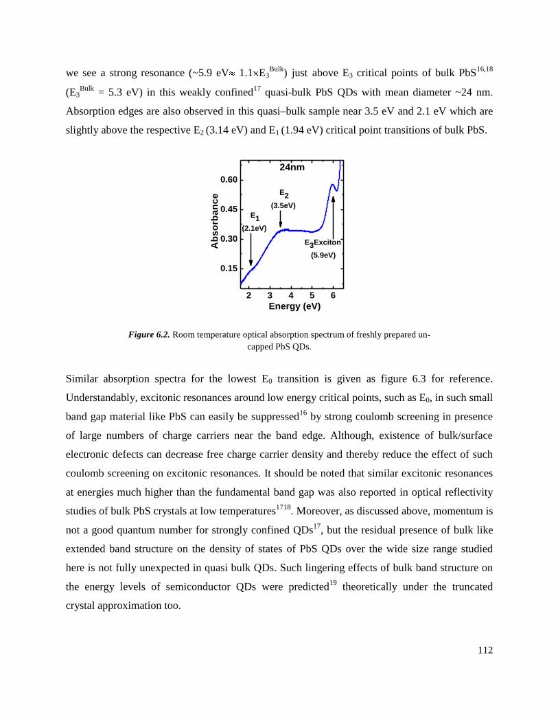
112
we see a strong resonance (~5.9 eV 1.1 E3Bulk
) just above E3 critical points of bulk PbS16,18
(E3Bulk
= 5.3 eV) in this weakly confined17
quasi-bulk PbS QDs with mean diameter ~24 nm.
Absorption edges are also observed in this quasi–bulk sample near 3.5 eV and 2.1 eV which are
slightly above the respective E2 (3.14 eV) and E1 (1.94 eV) critical point transitions of bulk PbS.
2 3 4 5 6
0.15
0.30
0.45
0.60
E1
(2.1eV)
E2
(3.5eV)
Ab
so
rba
nc
e
Energy (eV)
E3Exciton
(5.9eV)
24nm
Figure 6.2. Room temperature optical absorption spectrum of freshly prepared un-
capped PbS QDs.
Similar absorption spectra for the lowest E0 transition is given as figure 6.3 for reference.
Understandably, excitonic resonances around low energy critical points, such as E0, in such small
band gap material like PbS can easily be suppressed16
by strong coulomb screening in presence
of large numbers of charge carriers near the band edge. Although, existence of bulk/surface
electronic defects can decrease free charge carrier density and thereby reduce the effect of such
coulomb screening on excitonic resonances. It should be noted that similar excitonic resonances
at energies much higher than the fundamental band gap was also reported in optical reflectivity
studies of bulk PbS crystals at low temperatures1718
. Moreover, as discussed above, momentum is
not a good quantum number for strongly confined QDs17
, but the residual presence of bulk like
extended band structure on the density of states of PbS QDs over the wide size range studied
here is not fully unexpected in quasi bulk QDs. Such lingering effects of bulk band structure on
the energy levels of semiconductor QDs were predicted19
theoretically under the truncated
crystal approximation too.

113
800 1200 1600 2000 2400 2800
Q u a tz a s r e fe r e n c e
3 n m P b S
Q uartz as refernece
16nm PbS
2505 nm
Ab
so
rba
nc
e (
a.u
.)
1050 nm
water drop in chloroform
24nm PbS NCs in chloroform
2852 nm
Wavelength (nm)
Figure 6.3.E0 optical absorption transitions in different sized PbS QDs.
b. Size Variation and Blue Shift of E3 Resonance
In figure 6.4, we compare the optical absorption spectra of uncapped and TG capped PbS
QDs (having aB ~ 18 nm) of various diameters. Absorbance peak of E3 exciton resonance blue
shifts and increases monotonically with decreasing QDs size (as shown in the inset of the figure
6.4), which indicate that oscillator strength for excitonic absorption is still size dependent in PbS
QDs even under weak confinement Baradius 3~17
. The above enhancement of absorbance
with decreasing size clearly says that the contribution from light scattering is not significant.
Moreover, observed size dependence and blue shift also rules out the contamination due to TG
ligands or any other floating molecular species other than solid PbS as the cause of this E3
excitonic resonance. We see that E3 spectrum of this weakly confined PbS QDs having 24nm
crystallite diameter is gradually broadened into an absorption edge in ~16 nm PbS. Yet, below
16 nm, we observe progressive sharpening with decreasing size.

114
2 3 4 5 60.0
0.5
1.0
1.5
2.0
5 10 15 20 255.95
6.02
6.09
6.16
6.23
6.30
En
erg
y @
E3
(e
V)
Diameter(nm)
Ab
so
rba
nc
e
Energy (eV)
3nm
6nm
7nm
8nm
16nm
18nm
24nm
Figure 6.4.The variation of excitonic resonance with the size of PbS QDs. Molar
concentrations of PbS were kept same for all particle sizes during the measurements
except for 3 nm. There it was kept at 50% of the rest to avoid the saturation of optical
absorption. The inset shows change in E3 energy w.r.t. size of QDs.
Further understanding of this unusual evolution of excitonic broadening with crystallite
size will be presented near the end of Section III D and in the beginning of Section III E. These
spectra are fitted with Voigt line shapes from which we estimate both inhomogeneous width
(Gaussian) and homogenous width (Lorentzian) of the E3 resonance. Lorentzian widths are
nearly ~ 1.5 times the respective Gaussian widths for particles 16 nm. In general, magnitude of
excitonic transition is inversely proportional to its broadening parameter. Nevertheless,
inhomogeneous width of E3 exciton is not monotonically decreasing with size (figure 6.5).
Nominal use of Heisenberg uncertainty relation ~ tE with homogeneous broadening ( E)
estimates the life time ( t) of such states around femto-seconds domain.
Moreover, the magnitude of maximum possible energy broadening width Emax =
[ E(RMin) - E(RMax)] is calculated using R
e
mmR
hE
he 4
8.111
8
2
**2
2
, where Emax is
difference between the energy position for minimum (R=Rmin) and maximum (R=Rmax) QDs
radius, R=D/2 is the radius of the crystallite as estimated by XRD, h is the Planck constant, e
electronic charge, ε is the static dielectric constant, me*, mh* are the effective mass of electron
and hole.

115
0 5 10 15 20 25
0.0
0.1
0.2
0.3
0.4
Max =7.2)
Max =17)
Gaussian
Bro
ad
en
ing
wid
th (
eV
)Diameter (nm)
Figure 6.5. De-convoluted Gaussian component of the E3 excitonic line width has a
maximum around 16nm. Maximum possible energy broadening ( Emax) due to the size
distribution is much smaller than both the estimated inhomogeneous line widths for all
sizes.
These Emax values (figure 6.5) are well below the estimated line widths of E3 resonances
and have qualitatively different size dependence for all QDs diameters. Therefore, we can rule
out any size distribution effect towards energy broadening of E3 exciton. Surprisingly, excitonic
transitions (figure 6.6) are much above the E3 critical point of bulk PbS (0.6 eV larger than 5.3
eV) and also larger than its optical phonon energy ~20-27 meV12,20
. It should also be noted that
5.9 eV energy of E3 excitonic resonance is still < 2 E3Bulk
at 5.3 eV to observe such hot
excitonic effects around the E3 critical point. Although the energy of E3 excitonic resonance at
5.9 eV may be well within the energy continuum of states above the lowest fundamental E0
bandgap of PbS but it is certainly not the case for excitons localized around the much larger E3
gap16,18,19
. Nonetheless, estimates (using μ ≈ 0.05 me0, me
0 is the free electron mass) also shows
that this excess energy cannot be explained only by confinement induced enhancement of
energy**2
2 11
8 he
tConfinemenmmR
hE except for strongly confined PbS QDs of mean diameter ≤
3 nm (figure 6.6). Notably, no single power law behavior can describe the variation for all sizes.
So it is tempting to attribute this energy difference to – a) failure of effective mass theory21,22
at
smaller sizes, b) non-parabolicity23
of the band structure at high energies. However, size
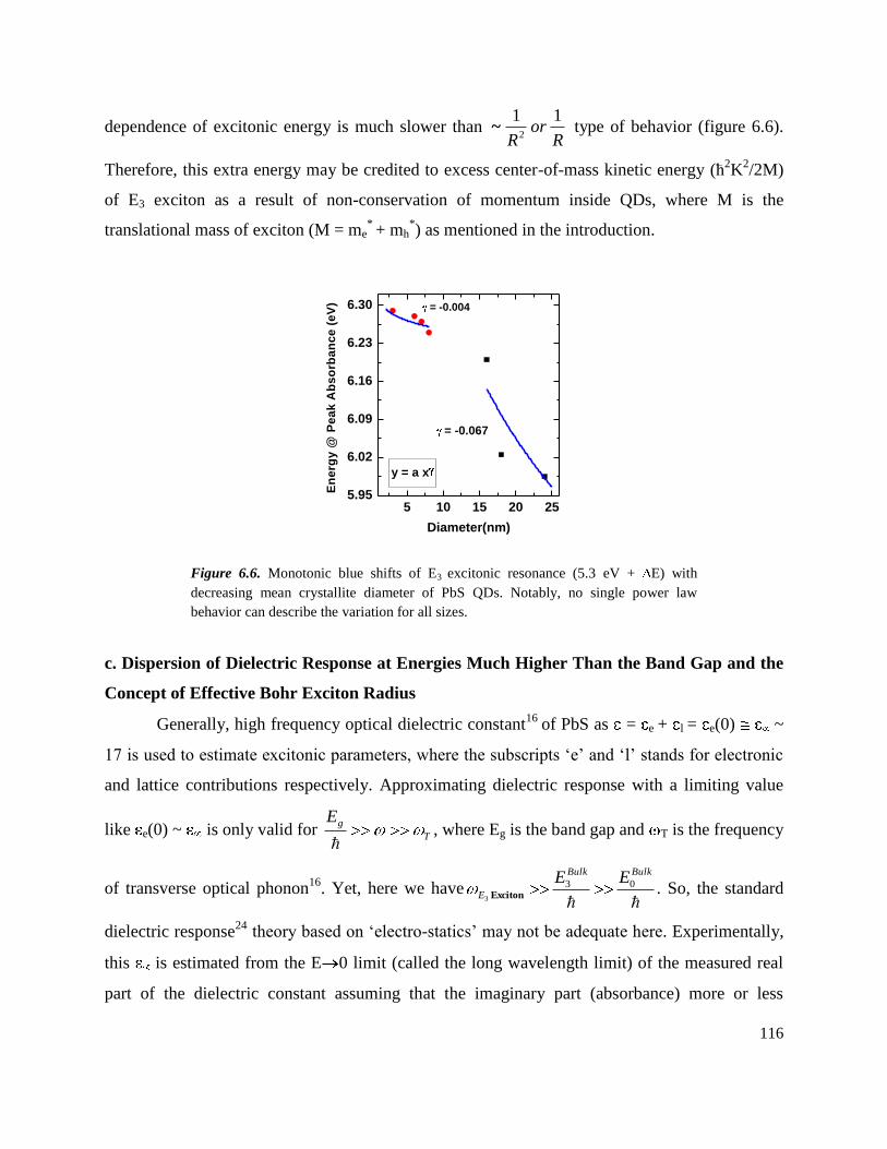
116
dependence of excitonic energy is much slower than R
orR
112
~ type of behavior (figure 6.6).
Therefore, this extra energy may be credited to excess center-of-mass kinetic energy (ћ2K
2/2M)
of E3 exciton as a result of non-conservation of momentum inside QDs, where M is the
translational mass of exciton (M = me* + mh
*) as mentioned in the introduction.
5 10 15 20 255.95
6.02
6.09
6.16
6.23
6.30
= -0.004
y = a x
En
erg
y @
Pe
ak
Ab
so
rba
nc
e (
eV
)
Diameter(nm)
= -0.067
Figure 6.6. Monotonic blue shifts of E3 excitonic resonance (5.3 eV + E) with
decreasing mean crystallite diameter of PbS QDs. Notably, no single power law
behavior can describe the variation for all sizes.
c. Dispersion of Dielectric Response at Energies Much Higher Than the Band Gap and the
Concept of Effective Bohr Exciton Radius
Generally, high frequency optical dielectric constant16
of PbS as = e + l = e(0) ~
17 is used to estimate excitonic parameters, where the subscripts ‘e’ and ‘l’ stands for electronic
and lattice contributions respectively. Approximating dielectric response with a limiting value
like e(0) ~ is only valid for T
gE
, where Eg is the band gap and T is the frequency
of transverse optical phonon16
. Yet, here we have
BulkBulk
E
EE 03
3 Exciton . So, the standard
dielectric response24
theory based on ‘electro-statics’ may not be adequate here. Experimentally,
this is estimated from the E 0 limit (called the long wavelength limit) of the measured real
part of the dielectric constant assuming that the imaginary part (absorbance) more or less

117
vanishes in that limit. However, in the presence of strong resonant optical absorption as
significant contribution from imaginary part of the dielectric response, we have used empirical
magnitude of 7.2 for complex ( ) around 5.9 eV of E3 excitonic resonance. This value of | ( )|
is estimated from the reported spectroscopic ellipsometry measurements on crystalline bulk
PbS25
. One can certainly measure | ( )| of these QDs to get a better estimate, which is currently
beyond the scope for wavelengths ≤ 210 nm. We have found that calculated exciton binding
energy R
eEEX
4
81 2.
using | ( )| = 7.2 are higher than that with =17 and much larger than
optical phonon energy of PbS for all sizes. Reader can see the quantitative details of this
variation of excitonic binding energy with size in the Table 6.1.
This can certainly explain the existence of E3 excitonic resonance in PbS QDs even at
room temperature. Assuming that we can still apply the hydrogenic model for exciton physics at
such energies, we approximate an effective Bohr exciton radius (a*
Ex) = 7.6 nm assuming | ( )| =
7.2 at E ~5.9 eV, μ ≈ 0.05 me0. Here we assume that an empirical dielectric response in terms of
( ) can be defined even for the smallest QDs without any additional size dependence and
surface polarization effects. This effective Bohr exciton radius (a*Ex)= 7.6 nm also shows that
quasi-bulk like uncapped particles with crystallite radius (diameter) of 12 nm (24 nm) can still be
treated in the weak confinement regime (radius ~3aB)17
. This value of | ( )| is much larger
around E2 , E1 , E0 critical points of PbS25
. Therefore, binding energy of any excitons around E2,
E1, E0 critical points can be much smaller than the binding energy hot excitonic resonance at E3
critical point. This certainly explains reason for not so significant presence of excitonic
resonance at low energy critical points as the presence of effectively large coulomb screening
effects16
as also explained in Section III A.

118
Table 6.1 Calculated exciton binding energy for PbS QDs using formula R
eEEX
4
81 2.
and ε
= 17 and ε = 7.2 respectively.
Samples ; Nano-Crystallite
Diameter (nm)
|EEX| (eV)
assuming = 17
|EEX| (eV)
assuming | | = 7.2
NO TG PbS ; 24 nm 0.013 0.030
20 TG PbS ; 18 nm 0.017 0.040
40 TG PbS ; 16 nm 0.020 0.045
60 TG PbS ; 8 nm 0.038 0.090
80 TG PbS ; 7 nm 0.044 0.103
100 TG PbS ; 6 nm 0.051 0.120
120 TG PbS ; 3 nm 0.102 0.240
d. Absence of Temperature Variation of Excitonic Resonance Even In Weakly Confined
QDs and the Significance of Non-Phonon Energy Relaxations.
Strong coupling of excitons to optical phonons is usually neglected in lead salts because
of quasi symmetrical nature of electron and hole bands near its fundamental band gap (E0).
However, electronic band structure near E3 critical point in PbS is definitely not symmetric (me
*
mh* ~E3)
16,26. So, we rather expect the broadening of E3 exciton to be dominated by Fröhlich
type strong polar exciton-phonon interactions27
. Despite of this, E3 resonance still survives at
room temperature and, most importantly, shows temperature independent shift of excitonic peak
(figure 6.7) even for weakly confined (~24 nm) particles. Therefore, it seems likely that ‘non-
phonon‟ energy relaxation mechanisms 27
like inverse Auger processes may be dominating over
phonons for this highly energetic E3 exciton. Further evidences of this assertion come from
temperature dependent evolution of excitonic spectra (figure 6.7a) of bigger QDs, which can be
ascribed to Auger cooling effects. This assertion is further vindicated by total absence of such

119
temperature dependence of absorption spectra in smaller QDs (figure 6.7c) which show no signs
of agglomeration with time (figure 6.9c) due to their charged nature unlike the bigger ones
(figure 6.9a). More details of this aging behavior can be found in Section III F. Extended band
structures of a solid are crucial for inverse Auger processes28-30
. This ‘hot’ E3 exciton can easily
avail a large number of final density of states required for efficient impact ionization via
confinement induced ‘zero phonon coupling’ to other parts of the PbS band structure in bigger
QDs8,9
. This leads to progressive enhancement of spectral broadening of larger ( 16 nm)
crystallites with decreasing size. Currently, probing any CM of this ‘hot’ E3 exciton with time
domain spectroscopy is beyond the scope due to scarcity of suitable deep-UV pulsed lasers at
wavelengths ≤ 210 nm. Typically, collisional broadening results in homogeneously broadened
line shapes for gas molecules. However, presence of significant inhomogeneous broadening due
to anisotropic exciton-exciton collisions can be explained by size confinement induced
momentum uncertainty which connects E3 excitons to different symmetry points in the PbS band
structure and a distribution in excitonic K space for such hot excitons.
2 3 4 5 60.0
0.2
0.4
0.6
0.8
1.0
1.2 (c)(b)
2 3 4 5 60.0
0.5
1.0
1.5
2.0
2.5
3.0
Ab
so
rba
nc
e
Energy (eV)
20o C
25o C
30o C
20o C Cooling
3nm
2 3 4 5 60.0
0.3
0.6
0.9
1.2
1.5
1.8
Ab
so
rba
nc
e
Energy (eV)
20oC
60oC
80oC
100oC
20oC cooling
16 nm
E3
Bulk edge
E3 Exciton
Ab
so
rba
nc
e
Energy (eV)
20oC
60oC
80oC
90oC
95oC
100oC
20oC
cooling
24nm
(a)
Figure 6.7. (a) Temperature variation of uncapped PbS QDs with mean diameter of 24 nm. (b) Almost
similar but less pronounced spectral changes with temperature are also observed for 16 nm PbS during
cooling stages. (c) 3 nm PbS shows relative less temperature dependence upto 30 C.

120
e. Mean Free Path of Excitonic Collisions and Effective Size Window For Efficient Multi-
Excitonic Effects.
Unlike monotonic size variation of the rates of inverse Auger type processes in smaller
QDs31-32
, spectral broadening of E3 exciton (figure 6.2 and 6.5) goes through a maximum around
intermediate confinement range. This observation can only be explained if impact ionization and
subsequent collisional broadening of E3 exciton have a minimum size cut off. Moreover, it was
predicted that exciton-exciton scattering33
and impact ionization34,35
are one of the main causes
of carrier multiplication in semiconductor QDs. However, impact ionization can be suppressed in
very small structures due to the presence of quasi ballistic transport36
. This usually happens when
the size (diameter) becomes smaller than the inverse Auger mean free path ( ) of exciton-exciton
scattering37
. Estimate based on such models37
yields nmaaTk
MEExEx
B
Ex 15931324
10
.~ ~**
.2
where D=2R~16 nm, M ≈ 0.21 me0,
0050e
m. , a*Ex=7.6 nm around E3, kB is Boltzmann
constant, T is temperature in Kelvin and EEx~1/R is the binding energy of E3 exciton. The values
of mean free path of exciton-exciton scattering for different sized QDs are given in the plot 6.8.
Interestingly, for 16nm PbS is comparable - (i) to the QDs diameter at the transition point of
both excitonic broadening (figure 6.5) and (ii) blue shift (figure 6.6) and (iii) the effective Bohr
exciton diameter (~15.2 nm) at E3 resonance. Use of = 17 produces >30 nm and one hardly
expects any PbS QDs having diameters < 30 nm to undergo MEG/CM in direct contradiction to
all experimental reports. However, if we invoke dynamic screening of coulomb interaction38,39
and | ( )| = 7.2 is used, then possibility of collisional broadening of E3 exciton within a
reasonable „size window‟ of operation is restored inside weak-to-intermediate confinement
regimes. This clearly resonates with the theoretical statement that strong confinement may not be
exclusively needed for efficient CM19
. Hence we seriously need to re-examine standard excitonic
terminologies to understand the physics of carrier multiplication of such ‘hot’ excitons38,39
– a)
having high center-of-mass velocity and b) created inside a region of dispersive dielectric
response which can deviate considerably from its usual high frequency limit of . It had also
been clearly emphasized39
that commonplace excitonic parameters like Bohr radius, exciton
binding energy can become “imprecise and ambiguous” within the framework of Bethe-Salpeter
equation which automatically accounts for such dynamical screening. We must however note

121
that, this expression of is calculated for symmetric S-states only and may need revision in
some cases.
0 5 10 15 20 25
15
20
25
30
35
40
Me
an
fre
e p
ath
(n
m)
Diameter (nm)
~ 17
~ 7.2
Figure 6.8. This plot demonstrates the comparison of exciton mean free path values
calculated using ε = 17 and ε = 7. In case of ε =17, the calculated mean free path for
exciton-exciton scattering event is >30 nm. In that case, any significant impact
ionization is not possible in any of the PbS QDs under our investigation due their
relative small sizes < 24 nm.
f. Role of Dielectric Confinement in the Aging of Absorbance Spectra and the Observed
Suppression of Aging in Smaller QDs.
To get further insights into E3 resonance, aqueous dispersion of PbS QDs of different
sizes are deliberately allowed to age and observed variation in optical absorbance are plotted in
figure 6.9. We see that, room temperature E3 excitonic spectra sharpen up with aging (figure 6.9a
and 6.9b) in bigger QDs. To understand, we briefly focus on the structural development of these
QDs during aging. Hydrodynamic size of uncapped PbS was already very large (>2 micron)
compared to its mean QDs diameter of 24 nm. The hydrodynamic size of fresh QDs with
diameter of 16 nm was ~30 nm, which gradually increases to around a micron due to aging.
However, XRD indicates (figure 6.10) that QDs size hardly increases during aging, which
excludes – (a) significant Ostwald ripening, (b) growth of PbS QDs by incorporation40
of sulfur
atoms from thiol based ligands. We understand this increase of hydrodynamic size can come
from agglomeration of PbS QDs which incidentally affect dielectric confinement41
of these

122
excitons. Overall decrease in absorbance (in spectral range < 5 eV) of QDs can be explained by
steady delocalization of excitonic wave function into surrounding material by increased
agglomeration and subsequent decrease of oscillator strength.
2 3 4 5 6
0.02
0.04
0.06
0.08
2 3 4 5 60
1
2
3
4
Ab
so
rban
ce
Energy (eV)
Fresh
1 hr
2 hrs
4 hrs
5 hrs
24 hrs
(c)(b)
2 3 4 5 60.0
0.5
1.0
1.5
2.016nm
Absorb
ance
Energy (eV)
Fresh
100 mins
150 mins
250 mins
450 mins
12 hrs
(a)
Ab
so
rba
nc
e
Energy (eV)
Fresh
50 mins
100 mins
200 mins
400 mins
12 hrs
24nm 3 nm
Figure 6.9. Aqueous dispersion of PbS QDs were not sonicated and deliberately allowed to age in
order to get better physical insights of the spectral origin of E3 exciton. (a) Variation of absorbance
of E3 exciton is characteristically opposite to the portion of the spectra at photon energies lower than
5 eV for uncapped PbS QDs with mean diameter of 24 nm. The abrupt changes between 3 eV to 4
eV are due to instrumental artifacts for lamp changes etc at small absorbance. (b) We see
qualitatively similar kind of sharpening of E3 excitonic peak with aging for 16nm PbS. (c) strongly
confined PbS nanoparticle with mean diameter 3 nm shows hardly any change with aging as
compared to that of 6.9a and 6.9b.
Nonetheless, E3 excitonic resonance is progressively enhanced and sharpened with aging!
Spatial delocalization of excitons can reduce confinement induced momentum uncertainty which
further reduce the availability of final states within the extended band structure of PbS. Hence,
probability of exciton-exciton scattering and collisional broadening of E3 exciton also comes
down with time. Here we must point out that even for the biggest PbS QDs with mean radius
12nm (figure 6.2), the spatial extent is well within the weak17
confinement region
nm6.7a; a3~radius*
ExB for all these quantum effects to influence the excitonic
delocalization. Additional defect formation or incorporation of water42
into the QDs cannot
explain such systematic but seemingly opposite aging dependence of – (a) the E3 excitonic
resonance and (b) the absorption spectra in lower energy ranges. Similar effect, although less

123
pronounced, is observed in 16 nm PbS (figure 6.9b). Here E3 exciton showed initial red shifts,
during aging induced gradual lessening of dielectric confinement, which was absent in larger
uncapped samples due to its quasi-bulk nature. Unlike 16 nm PbS, hydrodynamic diameter and
absorbance of smaller 3 nm PbS are hardly changing with time (figure 6.9c) This can only
happen if these smaller QDs are intrinsically charged as compared to the bigger ones. Mutual
coulomb repulsion of charged QDs can prevent agglomeration, sustain the dielectric environment
of 3 nm PbS and safeguard the absorbance from aging effect.
20 30 40 50 60 70 80
Inte
ns
ity
(a
.u.)
2 degree
16nm PbS QDs
16nm PbS in water for 24hrs
Figure 6.10. XRD spectra for 16nm PbS QDs. One spectrum is recorded on freshly
prepared QDs and for other spectra sample is intentionally kept in water for 24 hrs.
Drop casted thin films of each sample are used for measurements. It shows that aging
doesn’t changes crystallite size of ~16 nm PbS QDs. So, all changes observed in UV-
VIS absorption (figure 6.9b) of 16 nm PbS aging are due to agglomeration of QDs and
not due to Ostwald kind of growth of these QDs.
g. Suppression of Auger Cooling in Smaller QDs
As the E3 resonance ~ 5.9 eV is fading out with increasing temperature from 20 C to
100 C for uncapped quasi-bulk PbS (figure 6.9 a), another peak slowly emerges ~5.3 eV at its
expense. Interestingly, 5.3 eV is also the bulk E3 critical point of PbS! We see no gradual energy
shift of the E3 resonance with increasing temperature but rather a coexistence of E3 resonance
and the bulk like feature from 80 C to 95 C. Above that temperature, E3 resonance vanishes
altogether. However, we again retrieve this E3 resonance once temperature is reduced back to 20

124
C, except for some aging induced reduction in absorbance and sharpening of the E3 peak as
discussed in the previous section. PbS has a positive temperature coefficient of band gap except
under strong confinement regime where excitonic energy hardly13
varied with temperature.
However, we cannot use the same reasoning to explain current observations for this weakly
confined quasi-bulk PbS! With increasing phonon scattering and decreasing
LatticeCarrierHot T - TΔT above room temperature, this E3 exciton has much less access to other
parts of PbS band structure for efficient impact ionization. Therefore, emergence of bulk like
spectral feature ~5.3 eV with increasing temperature represent Auger cooling43,44
of energetic
‘hot’ E3 excitons to its bulk E3 band edge by transferring its excess energy mostly to heavier
holes (me*
mh* at E3)
19. Prominence of bulk E3 band edge steadily decrease with decreasing size
because of stronger size confinement and consequently lesser density of available ground states
at smaller sizes (figure 6.7b). Observed agglomeration (figure 6.7a and 6.7b) of these bigger QDs
(D 16 nm) also indicates their non-charged nature which may have prevented the suppression
of Auger cooling seen in smaller charged QDs
45 (figure 6.7c and 6.9c). QDs diameter also
remains same (figure 6.10) which confirms the absence of significant irreversible changes like
oxide/defect formation in this range of temperatures. Especially, line width broadening of E3
exciton with decreasing size and with increasing temperature are qualitatively different. In fact,
the temperature coefficient of impact ionization (TCII) depends on its threshold energy (Ei) and
the mean free path ( ) of exciton scattering as46
dTE
dE
dT
d
q
ETC
i
iiII . Spectra of 3nm PbS
QDs follows the literature47
for annealing temperatures >40 C, where it undergoes Ostwald
ripening and we also see that hydrodynamic size of these particles increases to >275 nm.
However, the E3 resonance did not change till 30 C. This apparent temperature independence of
excitonic line width for strongly confined PbS can be ascribed to a set of reasons like – (a)
reduction of impact ionization due to charged nature of these strongly confined particles, (b)
vanishing of TCII due to mutual cancellation of the above two terms, (c) reduction of collisional
broadening and Auger cooling in the ballistic regime, (d) strong surface effects etc. Size
dependence of photo-charging48,49
and/or photo-induced surface trapping50,51
are currently being
investigated.

125
Recently, it was argued that higher energy excitonic states are bulk like where Bohr
exciton radius (aB) can approach to ‘zero’ value due to the divergence of effective mass52
.
However, such ‘arithmetical’ divergence of effective mass happens 022 dkEd VC /, away from
E3 like critical points 0VCk EE . It is also evident that charged particles with smaller
effective masses are easy to accelerate and classical mechanical treatment of effective mass
approximation no longer holds where 222 dkEdm VChe // ,,* starts to diverge
53.
IV. Control Experiments
In order to understand the obtained results and to rule out any artifacts from temperature
dependent and time dependent measurements we have done some control experiment. The
results for these control experiments will further give insight into the presented conclusions.
a. Aging of Lead Acetate
Figure 6.11 shows aging of aqueous lead acetate with different time interval. Spectrum
has taken by dissolving lead acetate in water with water as reference. Peak feature at 5.9 eV
degrades in intensity with time which is just opposite to behavior for uncapped PbS QDs. It
shows the feature observed in aging of uncapped PbS QDs (6.9a) is not coming from presence of
unused lead acetate in the final product of PbS QDs.
2 3 4 5 60.0
0.5
1.0
1.5
2.0
2.5
3.0
3.5
Ab
so
rba
nc
e (
a.
u.)
Energy(eV)
fresh
after 100mins
after 4hrs
after 8hrs
after 24hrs
Aging of lead acetate
Figure 6.11. Aging of lead acetate at different time interval.

126
b. Lead Acetate Absorption Spectra at Different Temperature
Figure 6.12 shows effect of temperature on absorption spectra of aqueous lead acetate
solution. Spectra are taken by dissolving lead acetate in water with water as reference. With
increasing temperature absorption peak at 5.9 eV fades out and peak at 5.4 eV start appearing,
but lowering temperature back to 20 ˚C shows peak at 5.9 eV with no signature at 5.4 eV. This
behavior is similar to the uncapped PbS QDs. Similar spectral behavior and temperature
dependence (with figure 6.9b) just indicates that the molecular orbitals of E3 band structure may
be generically related with atomic orbitals of lead in lead compounds. However, we will clearly
demonstrate in the next section that the E3 resonance (Fig 6.2 and 6.4) is not coming from the
leftover Lead Acetate precursors. Moreover, we will also show in the next section that our
washing and purification sequence remove all such leftover reagents.
2 3 4 5 60
1
2
3
4
Ab
so
rba
nc
e (
a.
u.)
Energy(eV)
20oC
70oC
100oC
20oC cooling
Figure 6.12. Absorption spectra for lead acetate at different temperature.
IV) Control experiments to Rule out Presence of Artifacts and Unused
Chemicals or Ligands in the Optical Measurements of E3 Transition.
a. Water Absorption Spectrum
Figure 6.13 shows absorption Spectra of DI water with DI water as reference. No trace
of PbS like E3 peak found around 5.9 eV.This also indicates that reported E3 transition of PbS are

127
not due to any instrumental artifact or defects in cuvette or from water itself. So it indicates that
reported E3 transition of PbS are not due to any instrumental artifact or defects in cuvette.
2 3 4 5 6-0.010
-0.005
0.000
0.005
0.010
Ab
so
rba
nc
e (
a.u
.)
Energy(eV)
Figure 6.13. Absorption spectra for water with water as reference.
b. Absorption Spectra of Thioglycerol Capping Agent
Figure 6.14 shows absorption spectra of Thio-glycerol solution in de-ionized water with
deionized water as reference. It shows no resonance transition around 5.9 eV. Also the
absorption spectra for 24 nm uncapped QDs presented in the paper (Figure 6.2, 6.7a and 6.9a)
have no thioglycerol in it. Therefore, the E3 transition for PbS QDs (reported in manuscript)
cannot be from any unused Thio-glycerol (i.e. ligand) present in solution.
Figure 6.14. Absorption spectra for Thioglycerol with water as reference.

128
c. Absorption Spectra of Sodium Sulfide
Figure 6.15 shows absorbance of aqueous Sodium sulfide with deionized water as
reference. It shows absorption at 5.37 eV, indicating that E3 resonant absorbance of PbS QDs (>
5.9 eV) is not due to presence of unused sodium sulfide in the aqueous dispersion of PbS
nanoparticle used in optical absorption experiments.
2 3 4 5 60.0
0.2
0.4
0.6
0.8
Ab
so
rba
nc
e (
a.u
.)
Energy(eV)
Figure 6.15. Absorption spectra for Sodium Sulfide with water as reference.
d. E3 Resonance is Not Coming From Unused or Left Over Lead Acetate
Figure 6.16 shows absorbance spectra for mercapto-succinic acid capped CdTe QDs
and CdTe + additional Lead acetate solution, washed for 5 times. Here we have done the same
experiment with CdTe QDs which has no E3 like resonant peak to beginning with. We added
aqueous lead acetate solution (20 micro-liter of 0.02 M lead acetate in 3 ml of CdTe solution,
this is the full amount we add during the chemical synthesis in aqueous dispersion of CdTe and
then we washed it 5 time using centrifuge to prove that unused lead acetate won’t persist the
washing + purification sequence. Moreover, in case of PbS QDs, >99% of this 20 micro-liter
of lead acetate is expected to be used up in making PbS and only a very small fraction will be
left after the reaction with equal concentration of Na2S. So the E3 resonance peak is definitely
not coming from unused Lead Acetate either. It evidence that E3 excitonic resonance is not
coming from any leftover chemical reagents as our washing and purification sequence removes
it from the final aqueous dispersion of PbS QDs used in optical absorption experiments.

129
2 3 4 5 6
1E-3
0.01
0.1
1
No
rma
lize
d a
bs
orb
an
ce
Energy (eV)
CdTe
CdTe+Lead acetate washed 5 times
Figure 6.16. Absorption spectra for CdTe QDs and for CdTe QDs + lead acetate
solution with water as reference.
V. Conclusions In summary, dynamical Coulomb screening and the residual effect of extended band
structure of PbS were sought to explain the dependence of E3 excitonic resonance with aging and
temperature over a wide range nanoparticle sizes from weakly confined quasi bulk to strongly
confined very small QDs. We argue that Bohr radius of hot exciton is not material specific but
photo-excitation specific54
. This empirical notion of effective excitonic Bohr radius is a direct
consequence of the dynamical screening of coulomb interactions at high photon energies which
may eventually lead to better conceptual understanding of condensed matter physics of ‘hot’
excitons. Although it is not immediately clear whether one can use such a straight forward
extension of hydrogenic atom model to understand the formation of excitons at such high enough
energies. However, it is understandable that significant reduction of carrier multiplication in the
ballistic limit could have influenced all past studies focused only on strongly confined quantum
dots. As per our calculation in case of ε =17, the mean free path for exciton-exciton scattering
event is >30 nm. In that case, any significant impact ionization is not possible in any of the PbS
QDs under our investigation due their relative small sizes < 24 nm. However, if we use | ( )| =
7.2, then possibility of collisional broadening of E3 exciton within a reasonable „size window‟ of
operation is restored inside weak-to-intermediate confinement regimes. Therefore, we predict an

130
intermediate „size window‟, where impact ionization can dominate over other kinds of exciton
relaxation pathways. Although, this current 6 eV excitonic resonance has no relevance for
photovoltaics, but one can surely extend these analyses of hot exciton physics and even suggest
size optimization of semiconductor QDs for better exploitation of carrier multiplications to
improve the power conversion efficiency of nano-photovoltaics inside the solar spectrum.
Recently, it has been brought to our notice that enhancement of internal quantum efficiency of
PbSe quantum dots with increasing size is verified55
in experiments. While determining the
hydrodynamic sizes of the QDs using Dynamic Light Scattering we came across interesting
results here we could find out the exact result for the observed smaller hydrodynamic size
compare to the crystallite size. In the next Chpater 7, we have discussed these results in more
detail using Fluorescence Correlation Spectroscopy.

131
VI. References
1 A. J. Nozik, Multiple exciton generation in semiconductor quantum dots, Chem. Phys. Lett.
457, 3-11, 2008.
2 W. Schockley and H. J. Queisser, Detailed Balance Limit of Efficiency of p-n Junction Solar
Cells, J. Appl. Phys. 32 (3), 510, 1961.
3 S. Kolodinski and J. Werner, Solar Energy. Mat. And Solar cells 33, 3, 275, 1994.
4 A. J. Nozik, Quantum dot solar cell, Physica E 14, 115, 2002.
5 G. N. Lazaro, A. Padilha, L. Levina, V. Sukhovatkin, S. Webster, L. Brzozowski, E. H.
Sargent, D. J. Hagan and Eric W. Van Stryland, Size dependence of carrier dynamics and
carrier multiplication in PbS quantum dots, Phys. Rev. B, 83, 155302, 2011.
6 R. D. Schaller and V. I. Klimov Phys. Rev. Lett. 92, 186601, 2004 ; R. D. Schaller, M. Sykora,
J. M. Pietryga and V. I. Klimov, Nano Lett. 6, 424, 2006.
7 R. J. Ellingson, M.C. Beard, J. C., Johnson, P. Yu, O. I. Micic, A. J. Nozik, A. Shabaev and A.
L. Efros, Highly Efficient Multiple Exciton Generation in Colloidal PbSe, Nano Lett. 5, 865,
2005.
8 J. J. H. Pijpers, R. Ulbricht, K. J. Tielrooij, A. Osherov, Y. Golan, C. Deleure, G. Alla and, M.
Bonn, Assessment of carrier-multiplication efficiency in bulk PbSe and PbS, Nature Phys. 5,
811, 2009.
9 C. Deleure, G. Allan, J. J. H. Pijpers and M. Bonn, Carrier multiplication in bulk and
nanocrystalline semiconductors: Mechanism, efficiency, and interest for solar cells Phys. Rev.
B 81, 125306, 2010.
10 G. Nair, S. M. Geyer, L.-Y. Chang and M. G. Bawendi, Carrier multiplication yields in PbS
and PbSe nanocrystals measured by transient photoluminescence, Phys. Rev. B 78, 125325,
2008.
11 G. Nair and M. G. Bawendi, Carrier multiplication yields of CdSe and CdTe nanocrystals by
transient photoluminescence spectroscopy, Phys. Rev. B 76, 081304R, 2007.
12 T. D. Krauss and F. W. Wise, Raman-scattering study of exciton-phonon coupling in PbS
nanocrystals, Phys. Rev. B 55, 9860, 1997.

132
13
A. Olkhovets, R. C. Hsu, A. Lipovskii, and F. W. Wise, Size-Dependent Temperature
Variation of the Energy Gap in Lead-Salt Quantum Dots, Phys. Rev. Lett. 81, 3539, 1998.
14 F. W. Wise, Lead Salt Quantum Dots: the Limit of Strong Quantum Confinement, Acc.
Chem. Res. 33, 773, 2000.
15 B. R. Hyun et al. Role of solvent dielectric properties on charge transfer from PbS
nanocrystals to molecules. Nano Lett. 10, 318, 2010.
16 Yu P and Cardona M Fundamentals of Semiconductors (Springer-Verlag, Berlin Heidelberg
1999), 2nd
edition, Chapter 6.
17 A. I. Ekimov et al. Absorption and intensity-dependent photoluminescence measurements on
CdSe quantum dots: assignment of the first electronic transitions, J. Opt. Soc. Am. B 10, 100,
1993.
18 S. E. Kohn, P. Y. Yu, Y. Petroff, Y. R. Shen, Y. Tsang and M. L. Cohen M L, Electronic Band
Structure and Optical Properties of PbTe, PbSe, and PbS, Phys. Rev. B 8, 1477, 1973. See
figure 12 and subsequent discussions as well as to a list of such higher energy excitonic
transitions in lead salts mentioned in Table 1.
19 J. W. Luo, A. Franceschetti and A. Zunger, Carrier multiplication in semiconductor
nanocrystals: theoretical screening of candidate materials based on band-structure effects,
Nano lett. 8, 3174, 2008.
20 A. Nozik, Quantum dot solar cell, Physica E 14, 115, 2002.
21 M. S. Hybertsen, Absorption and emission of light in nanoscale silicon structures, Phys. Rev.
Lett. 72, 1514, 1994.; C. Delerue, G. Allan and M. Lannoo, Theoretical aspect of luminescence
of porous Si, Phys. Rev. B 48, 11024, 1993.
22 S. Datta and K. L. Narasimhan, Model for physical absorption in porous Si, Phys. Rev. B 60,
8246, 1999.
23 Y. Wang, A. Suna, W. Mahler and R. Kasowski, PbS in polymers from molecules to solids. J.
Chem. Phys. 87, 7315, 1987.
24 S. Schmitt-Rink, D. A. B. Miller and D. S. Chemla,Theory of the linear and nonlinear optical
properties of semiconductor microcrystallites, Phys Rev. B 35, 8113, 1987. Refer to equation
19.

133
25
H. Kanazawa and S. Adachi, Spectroellipsometry and electroreflectance of PbS, J. Appl. Phys.
83, 5997, 1988.
26 A. Franceschetti, Structural and electronic properties of PbSe nanocrystals from first
principles, Phys. Rev. B 78, 075418, 2008.
27 V. I. Klimov, Optical Nonlinearities and Ultrafast Carrier Dynamics in Semiconductor
Nanocrystals, J. Phys. Chem. B 104, 6112, 2000.
28 M. Stobbe, R. Redmer and W. Schattke, Impact ionization rate in GaAs, Phys. Rev. B 49,
4494, 1994.
29 L. Tirino, M. Weber, K. F. Brennan, E. Bellotti and M. Goano M, Temperature dependence of
the impact ionization coefficients in GaAs, cubic SiC, and zinc-blende GaN, J. Appl. Phys. 94,
423, 2003.
30 J. Y. Tang and K. Hess, J. Appl. Phys. 54, 5139, 1983.
31 V. I. Klimov, A. A. Mikhailovsky, D. W. McBranch, C. A. Leatherdale and M. G. Bawendi,
Quantisation of multiple auger states in semiconductor nanoparticles. Science 287, 1011, 2000.
32 V. I. Klimov, A. A. Mikhailovsky, S. Xu, A. Malko, J. A. Hollingsworth, C. A. Leatherdale,
H. J. Eisler and M. G. Bawendi, Optical gain and stimulated emission in nanocrystals quantum
sots, Science 290, 314, 2000.
33 A. Piryatinski and K. A. Velizhanin, An exciton scattering model for carrier multiplication in
nanocrystals: Theory, J. Chem. Phys. 133, 084508, 2010.
34 A. Franceschetti, J. M. An and J. Zunger J, Impact ionization can explain carrier multiplication
in PbSe quantum dots, Nano Lett. 6, 2191, 2006.
35 G. Nootz, L. A. Padilha, L. Levina, V. Sukhovatkin, S. Webster, L. Brzozowski, E. H.Sargent,
D. J. Hagan and E. W. VanStryland, Size dependence of carrier dynamics and carrier
multiplication in PbS quantum dots, Phy. Rev. B 83, 155302, 2011.
36 N. Sano and M. Tomizawa and A. Yoshii, IEEE Transaction on electron devices 42, 2211,
1995.
37 G. A. Thomas, A. Frova, J. C. Hensel, R. E. Miler and P. A. Lee, Collision broadening in the
exciton gas outside the electron-hole droplets in Ge, Phys. Rev. B 13, 1692, 1976.

134
38
S. DasSarma and D. W. Wang, Many-Body Renormalization of Semiconductor Quantum
Wire Excitons: Absorption, Gain, Binding, and Unbinding, Phys. Rev. Lett. 84, 2010, 2000;
Wang D W, and DasSarma S, Phys. Rev B. 64, 195313, 2001.
39 Meyer J R and Bartoli F J Dynamic dielectric response to electron-hole and electron-electron
interactions, Phys. Rev B 28, 915, 1983.
40 A. L. Rogach, Covalent bound CdTe nanocrystals, Mat. Sci. and Eng B 69-70, 435, 2000.
41 M. G. Lisachenko, E. A. Konstantinova, P. K. Kashkarov and V. Timoshenko Yu, Dielectric
effect in Si quantum wires, Phys. Stat. Sol. (a) 182, 297, 2000.
42 S. W. Buckner, R. L. Konold and P. A. Jelliss, Luminescence quenching in PbS nanoparticles,
Chem. Phys. Lett. 394, 400, 2004.
43 M. Califano M, J. Phys. Chem. C 112, 8570, 2008.
44 E. Hendry, M. Koeberg, F. Wang, H. Zhang, C. De M. Donega, D. Vanmaekelbergh and M.
Bonn, Direct observation of electro to hole energy transfer in CdSe quantum dots. Phys. Rev.
Lett. 96, 057408, 2006.
45 M. Califano, Giant suppression of auger electron cooling in charged nanocrystals, Appl. Phys.
Lett. 91, 172114, 2007.
46 N. S. Waldron, A. J. Pitera, M. L. Lee, E. A. Fitzgerald and J. A. Alamo, Positive temperature
coefficient of impact ionization in strained Si, IEEE Transactions on Electron Devices 52,
1627, 2005.
47 L. Turyanska et. al.Tailoring physical properties of PbS quantum dots by thermal annealing,
Nanotechnology 20, 315604, 2009.
48 J. A. McGuire, M. Sykora, I. Robel, L. A. Padilha, J. Joo, J. M. Pietryga and V. I. Klimov,
Spectroscopic signature of photocharging due to hot-carrier transfer in solution of
semiconductor nanocrystals under low-intensity ultra-violet excitation. ACS Nano, 4, 6087,
2010.
49 A.V.R. Murthy, Padmashri Patil, Shouvik Datta, Shivprasad Patil, Photoinduced dark fraction
due to blinking and photodarkening probability in aqueous CdTe quantum dots. J. Phys. Chem.
C. 117, 13268-75, 2013.
50 M. Califano, Photoinduced Surface Trapping and the Observed Carrier Multiplication Yields
in Static CdSe Nanocrystal Samples, ACS Nano, 5, 3614, 2011.

135
51
P. Tyagi and P. Kambhampati, False multiple exciton recombination and multiple exciton
generation signals in semiconductor quantum dots arise from surface charge trapping, J. Chem.
Phys. 134, 094706, 2011.
52 B. Cho, W. K. Peters, R. J. Hill, T. L. Courtney and D. M. Jonas, Bulk like hot carrier
dynamics in PbS quantum dots, Nano Lett. 10, 2498, 2010.
53 C. F. Klingshirn C F Semiconductor Optics, (Springer, Berlin, 1997) Chapter 10.
54 Z. Lin, A. Franceschetti and M. T. Lusk, Size dependent multiple exciton generation rate in
CdSe quantum dots. ACS Nano, 5, 2503, 2011.
55 O. E. Semonin, J. M. Luthe, S. Choi, H-Y. Chen, J. Gao, A. J. Nozik and M. C. Beard, Peak
exciton quantum efficiency exceeding 100% via MEG in quantum dot solar cell. Science 334,
1530, 2011.

136

137
Chapter 7
Effect of Blinking on Hydrodynamic Size
Measurement
I. Introduction
As we have seen before in the introduction chapter, the usefulness of semiconductor QDs
for variety of device applications made this area attractive for research. Different useful
properties of these QDs are the key to the success of various leading innovations in
biomedical1,2,3,4,5,6
research, electronics7 and opto-electronics
8 industry. However, physical
properties of the nanoparticles (NPs) are primarily dependent on the amount of spatial
confinement of charge carriers i.e. size of NPs. This characteristic size is measured by few
different approaches depending on the interest, like hydrodynamic size and crystallite size.
Crystallite sizes are usually measured by X-ray diffraction and transmission electron microscopy.
The crystallite size measures physical size of NP which consist mainly the part with crystallite
planes and includes constituents of the NP only. Whereas, the hydrodynamic size also measures
the small additional layer of capping ligands and the effective overall size due to interaction of
NPs with surrounding solvent in addition to the solid core crystallite. The two approaches of
measurements are qualitatively described in figure 7.1.
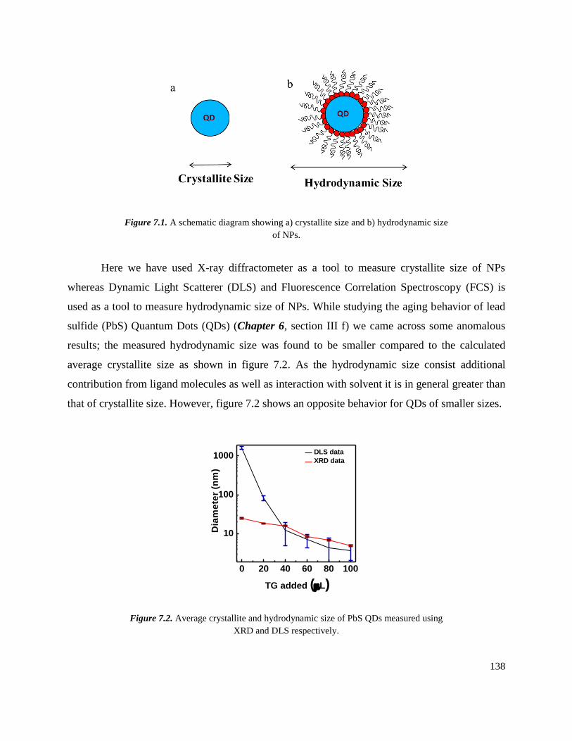
138
Figure 7.1. A schematic diagram showing a) crystallite size and b) hydrodynamic size
of NPs.
Here we have used X-ray diffractometer as a tool to measure crystallite size of NPs
whereas Dynamic Light Scatterer (DLS) and Fluorescence Correlation Spectroscopy (FCS) is
used as a tool to measure hydrodynamic size of NPs. While studying the aging behavior of lead
sulfide (PbS) Quantum Dots (QDs) (Chapter 6, section III f) we came across some anomalous
results; the measured hydrodynamic size was found to be smaller compared to the calculated
average crystallite size as shown in figure 7.2. As the hydrodynamic size consist additional
contribution from ligand molecules as well as interaction with solvent it is in general greater than
that of crystallite size. However, figure 7.2 shows an opposite behavior for QDs of smaller sizes.
0 20 40 60 80 100
10
100
1000
Dia
me
ter
(nm
)
TG added (L)
DLS data
XRD data
Figure 7.2. Average crystallite and hydrodynamic size of PbS QDs measured using
XRD and DLS respectively.

139
Initially we thought that the smaller sized QDs are undergoing photo induced
fragmentation while it is being excited by laser. However, such kind of fragmentation of NPs
into smaller NPs happens only at or > 90 mW intensity9,10
whereas in DLS the intensity of laser
used for excitation is hardly 3- 4 mW. So to find out the reason behind this ambiguity we
decided to do more experiments using FCS in collaboration with Dr. Shivprasad Patil‟s research
group in IISER Pune. However, we could not use PbS QDs in these FCS measurements as the
FCS only works with measurement of fluorescence fluctuation and fluorescence intensity from
PbS QDs was considerably smaller than CdTe QDs. Therefore, in order to do this experiment we
used fluorescent CdTe QDs, these QDs are synthesized as explained in Chapter 3. Out of the
various available sizes, we have used only four differently sized CdTe QDs for our study using
FCS11
.
II. Materials and Methods
II. a. Fluorescence Correlation Spectroscopy (FCS)
FCS can be used to measure average number of luminescent particles in its detection
volume12,13,14,15
. We have used a home-built FCS setup available with Dr. Shivprasad Patil‟s
group for all the measurements mentioned here. A diode laser of 532 nm, TEM00 mode (Dream
lasers, China) was used as a photo excitation source. Excitation intensity is varied using a
combination of neutral density filters from 3.3 kW/cm2 to 145 kW/cm
2. FCS setup was calibrated
by a standard fluorescent dye Rhodamine 6G (RH6G).
II. b. CdTe Quantum Dots
We have used four differently sized CdTe QDs in these measurements. The QDs are
characterized using UV-VIS absorption and Photoluminescence spectroscopy and corresponding
spectra is given in the figure 7.3. We have recorded a series of absorption spectra at various
dilutions. A molar extinction coefficient of 5.6×10⁴
mol−1
cm−1
is measured from the
concentration versus peak absorbance data. The average diameters of these CdTe QDs are 3.4
nm, 4.1 nm, 4.2 nm and 4.5 nm respectively. The size of QDs noted here is calculated by
applying effective mass approximation (EMA) formula16,17,18
to its excitonic peak position in the

140
optical absorbance spectra. The absorption cross section is determined following ref19
. The
absorption cross section of QD with size 4.2nm is 2 ×10⁻¹⁶
cm2. After complete characterization,
QD samples are further diluted for FCS study.
400 500 600 700 800
(b)
400 500 600 700 800
No
rma
lize
d I
nte
ns
ity
Wavelength(nm)
3.4 nm
4.1 nm
4.2 nm
4.5 nm
3.4 nm
4.1 nm
4.2 nm
4.5 nm
A
bs
orb
an
ce
(a
.u.)
Wavelength(nm)
(a)
Figure 7.3. a) Absorbance spectra and b) photoluminescence spectra for the as
prepared CdTe QDs.
III. Results and Discussions
a. FCS Study of QDs with Different Excitation Intensity
We have studied autocorrelation curves for 4.2 nm QDs at different excitation intensities
starting from lowest available intensity ~3.3 kW/cm2 to highest intensity ~145 kW/cm
2. For this
study we have used extremely dilute aqueous solution of QDs. An analytical expression (7.1)
describing nanoparticles diffusion is fitted for the autocorrelation data obtained from different
excitation intensities20,21,22,23
.
2
1
D
2
Dl
r11N
1)(G
(7.1)
Here, the τD is the diffusion time or average residence time spent by luminescent QDs in the
detection volume. This is the only characteristic time one get using this equation. Parameters r

141
and l are radial and axial dimensions of the detection volume respectively. The average number
of fluorescent particles in the detection volume can be calculated by taking inverse of
autocorrelation at zero time lag. The measured autocorrelations and fits to 3 D diffusion equation
at different excitation intensities for 4.2 nm CdTe QDs is shown in the upper part of figure 7.4.
The plot at the bottom is a representative fit at 145 kW/cm2 showing the quality of the fit.
101
102
103
104
0.0
0.3
0.6
0.9
G (
Lag time (s)
Intensity
-0.03
0.00
0.03
Resi
du
als
Figure 7.4. Autocorrelation curves obtained for 4.2nm QD excited at different
intensities. The plot at the bottom shows residual after fitting the data equation 7.1.
The dots represent obtained data and continuous black lines are the fits to the dots.
After fitting individual curves of figure 7.4 and using fit parameters, we have calculated
values of τD and N i.e. diffusion time and average number of QDs in the detection volume
respectively. The values of τD decreases with increase in photo-excitation intensity on other
hand τD values for standard dye rhodamine (Rh6G) remains constant as shown in figure 7.5a.
The direct indication of this result is that the size of the particles is decreasing as the excitation
intensity increases i.e. particles are undergoing fragmentation. This cannot be true as the value
for number of particles in the detection volume decreases as shown in figure 7.5b. Further
observations are based on the estimated values of N for different excitation intensity as shown in
figure 7.5b. These values of N initially decreases with intensity and after a while remain constant
with increasing excitation intensity. At this we came across the phenomenon of „blinking‟24,25,26
.
in QDs and realized that this luminescence intermittency or „blinking‟ events may explain the
obtained results. Many researchers have tried to model blinking using Monte Carlo simulations,

142
stretched exponents and multiple exponents27
. Though the exact reason for intermittency is not
known24,28,29,30,31
, experiments revealed that the random “on” and “off” states in luminescence
blinking occurs at all-time scale24,25,26
. It is important to understand the photo-physics of
luminescence blinking from single QD in aqueous solution as the “off” state affects ensemble
quantum yield32
and restricts advances in QD technology where a single QD is used33
. It is also
known that the blinking can be suppressed by the addition of thiols to a colloidal solution of
QDs34
.
101
102
103
104
0.0
0.2
104
105
2.5
3.0
3.5
4.0
104
105
50
100
150
200
Intensity (W/cm2) Intensity (W/cm
2)
N
4.2nm- QD
D
s)
4.2nm- QD
Rh6G
Figure 7.5. a) Dependence of diffusion time on the excitation intensity. b) Dependence of
average number of QDs on intensity.
So we argue that blinking is the main reason for observing decrease in diffusion time and
average number of QDs in detection volume as shown in schematic diagram 7.6a. As the QDs
undergoes „off‟ state while diffusing through the detection volume, the calculated number of
QDs for particular intensity (figure 7.5b) is not the actual number of QDs present in detection
volume. So we refer to this number as the apparent average number of QDs i.e. Napp. The actual
number of QDs, both in dark and luminescent states which is higher than this, and we refer to it
as Nactual. The measurements in figure 7.5b provide us an estimate of Napp. Further we attribute
the reduction in τD to an apparently reduced detection volume due to a blinking QD. The cartoon
in Figure 7.6b describes this concept. When a QD enters into the detection volume it starts to
blink. While calculating autocorrelation a QD becoming dark is not different from a QD leaving
the detection volume. Similarly, a QD becoming luminescent again is identical to a QD entering
the detection volume. Therefore, the effective detection volume seen by a blinking QD is less

143
than the actual detection volume. This actual detection volume is usually measured using a
standard fluorophore (Rh6G) with a known diffusion coefficient in a given medium. Due to the
apparently reduced detection volume, the measured average residence time of blinking QD is
less than its actual value. A close inspection of figure 7.5a reveals that at low excitation intensity,
the τD does not change much with intensity and remains constant around 200 μs. From this value
of τD and using the Stokes−Einstein relationship, we determined the hydrodynamic radius to be 3
nm. This matches well with the estimated radius of these QDs (2.2 nm) using the effective mass
approximation to its excitonic absorption spectrum. The above result suggests that blinking does
not affect measurement of the hydrodynamic radius of these CdTe QDs using FCS at lower
intensities.
Figure 7.6. a) Schematic showing detection volume and effect of addition of BME on “ON” state of
QDs b) Schematic describing „apparently reduced detection volume‟ for blinking QDs.
b. Suppression of Blinking by Addition of BME
In this section we will prove the concept of apparent reduced detection volume and the
apparent average number of QDs. We have performed same experiments after addition of BME
to an aqueous solution of QDs, which make these QDs non-blinking. If the QDs are non-blinking
then the “excluded volume” should not appear in the experiments and we should get back actual
detection volume. Moreover, here the diffusion time τD should provide the correct hydrodynamic
radius. Since thiol addition is known to suppress blinking32,34,35
we have added 1mL of 100μM
BME to an aqueous solution of QDs. As blinking affects ensemble quantum yield of a

144
nanoparticle, the per particle brightness (PPB) should increase after addition of BME. We have
observed that the count rate as well as PPB increased from 19×103
s−1
to 36×104
s−1
and from
6×10³
s‑1 to 18×10
3 s
−1, respectively. Figure 7.7 shows autocorrelation curves before and after
addition of BME at 145 kW/cm2.
Figure 7.7. Autocorrelation curves for 4.2 nm QD before and after addition of BME a)
excited at 145 kW/cm2 intensity b) excited at 3.3 kW/cm
2 intensity.
We observed that after BME addition simple 3D diffusion fit equation (equation 7.1)
does not fit to the autocorrelation instead, an analytical expression of equation 7.2 describing a
diffusion kinetics plus single “on−off” rate fits to autocorrelation data. Equation 7.2is typically
used in FCS analysis where a chemical reaction involving the luminescence “on−off” state along
with diffusion contributes to the equilibrium intensity fluctuations20,21,22,23
.
2
1
D
2
D
)l
r(11N
1e
F1
F1)(G r
(7.2)
Note that in this equation there are two characteristic time scale; one is τD which explains
the diffusion time or average resident time spent by fluorescent molecule in detection volume.
The second one is τr, which is a characteristic time needed to reach an equilibrium number of
dark and bright populations and so the rate is reaction rate kr = 1/τr. The kr is the sum of forward
and backward rates in reaction causing luminescence22
. F is the equilibrium dark fraction in
dark−bright conversion22
. After BME addition the luminescence fluctuations are caused due to

145
(a) fluorophores moving in and out of the detection volume because of diffusion, and (b)
switching between “on” and “off” luminescence states of fluorophores with a single rate to attain
equilibrium. Table 7.1 shows various parameters obtained by fitting 3D diffusion equations 7.1
and equation7.2 to measured autocorrelations in Figure 7.7a. As mentioned above, 3 D diffusion
equation fits to autocorrelations without BME addition, whereas equation 7.2 fits to
autocorrelations with BME addition. Both of these measurements are performed at 145 kW/cm2
excitation intensity.
TABLE 7.1: Fit parameters are described before and after BME addition to QDs solution.
(a) Average number of particles (N) (b) Diffusion time (τD) (c) Electron exchange rate (kr)
(d) Equilibrium dark fraction (F)
Sample
Fit parameters at 145 kW/cm2
N (a)
τD (µs) (b)
kr (µs) (c)
F (d)
QDs without BME 2.96 ± 0.01 40.96 ±
0.67
- -
QDs with BME
above 70 µM
4.74 ± 0.02 160.96 ± 11 28.3 ± 1.67 0.426 ± 0.01
From fit parameters, it is clear that the diffusion time after the addition of BME is
recovered and now determines the hydrodynamic radius reasonably well. This supports the
concept of “apparently reduced detection volume” presented in the previous section IIIa.
Additionally, the fitting of equation 7.2 means that luminescence after the addition of BME
fluctuates with a single rate kr = 1/τr2222
. τr = 28.3 ± 1.67 μs in the present experiment. The fit
value of 0.426 ± 0.01 for F also suggests that nearly 40% of the QDs are dark in equilibrium
dark−bright conversion, yet all of them contribute to N20,21,22
. A nonzero value for τr indicates
that the addition of BME does not suppress luminescence fluctuations at all-time scales. This
does not contradict the previous evidence of blinking suppression using BME since those
measurements employ millisecond binning times34
. After BME addition the average number of
QDs in the detection volume increases from 2.96 ± 0.01 to 4.74 ± 0.02 (Table 7.1). The effect of
BME addition on average number of QDs in the detection volume is shown in figure 7.8b.

146
Figure 7.8. Effect of gradual addition of BME on a) diffusion time and b) average
number of QDs in the detection volume.
In a collection of QDs there are blinking, non-blinking and non-radiant QDs36
. As name
suggests the non-radiant QDs remain dark at all times so in our measurement we are concerned
only with blinking and non-blinking QDs. If we assume that addition of BME recovers all
blinking QDs from their dark state then the actual number of QDs in the detection volume is
Nactual = 4.74 ± 0.02. As there is no evidence that long lived non-radiant QDs fully recover due to
addition of BME, so the Nactual does not include them. Now the difference ΔN = Nactual −Napp =
4.74 − 2.96 = 1.78 and the dark fraction due to blinking is f = ΔN/Nactual= 0.37. It should be
noted here that, the equilibrium dark fraction F, and the equilibrium dark fraction f due to
blinking are not same. At very low intensity ~3.3 kW/cm2, the addition of BME does not have
any effect on FCS measurements. Figure 7.7 b shows autocorrelations for both before and after
addition of BME at 3.3 kW/cm2, importantly 3D diffusion equation 7.1 fits to both the
autocorrelation curves before and after BME addition. Note that we are measuring τD and N by
fitting the equations to data starting from 10 μs. This range is typically avoided in FCS
measurements owing to photo-bleaching in the case of fluorophores22
and rotational dynamics in
the case of nanostructures37
. We monitor fluorescence intensity trace at the time of experiment
and the laser intensity used in our experiments is in the range of a few microwatts to a maximum
of 500 μW only. So, if the QDs are suffering from photo-bleaching, average fluorescence
intensity and per particle brightness should decrease within the autocorrelation record time (100
s). We did not observe these effects related to photo-bleaching. Secondly if the QDs are
undergoing photo-bleaching then the equation describing only diffusion does not fit

147
autocorrelation properly. However, it fits very well in our experiments. We could not capture
polarization of emission light which excludes effects of rotational dynamics on autocorrelation
curves.
c. Required Number of BME Molecules per QD to Suppress Blinking
In this section we discuss how many number of BME molecules are needed per QD to
suppress blinking? In order to do this measurement we have added controlled amount of BME to
the 1ml of diluted QDs dispersion solution. The excitation intensity is kept constant 145 kW/cm2
and autocorrelations are measured after each addition of BME. The data is plotted in figure 7.8
shows average number of QDs (N) versus BME addition. Initially the number of QDs is
increases slowly, then changes rapidly and finally saturates. This growth is modeled with a
sigmoid growth given by Hill equation, θ = θmax[xn/(kn +xn)]38
. Here, θ is number of QDs
recovered from photo-darkened state by BME addition and x is the concentration of BME
molecules needed to recover half of the QDs from photo-darkened state. Calculations show that
~70 μM BME is required, i.e. 104 BME molecules are required to recover QDs from photo-
darkened state by using value of detection volume 0.95 fL.
d. Dark Fraction (f) and photo-darkening Probability (P)
The Dark fraction (f) in dark-bright conversion is measured using FCS at different
excitation intensity and is given as f = ΔN/Nactual. The measured dark fraction (f) due to blinking
at different excitation intensity is as shown in figure 7.9. A straight line fits to the data and yields
slope 1.2 ×10⁻⁶
cm2/W. The dependence of dark fraction on excitation intensity suggests that dark
state in blinking is photo-induced and the linear dependence on intensity suggests that it is a one-
photon process.

148
0.0 2.0x10⁵
4.0x10⁵
0.5
1.0
Ph
oto
-da
rk
en
ed
fra
cti
on
Intensity (W/cm2)
Figure 7.9. Photo-darkened fraction verses excitation intensity.
From figure 7.9 we can compute the probability of a QD becoming dark after absorption of a
photon i.e. photo-darkening probability. Now the photo-induced dark fraction in our experiment
must be equal to the product of photo-darkening probability P and number of photons absorbed n
(i.e. f = P × n). Here, the number of photons absorbed „n‟ can be computed if we know the
absorption cross-section ρ, the excitation intensity I in kW/cm2, the frequency of excitation υ and
the illumination time t, then the n = Iρt/hυ29
.
Therefore,
htI
Pf
Now, theoretically the slope of the straight line (figure 7.9) is Pρt/hυ which is 1.2 × 10
-6 cm
2/W.
We have further computed value of P = 9 × 10⁻⁶
. For this calculations we have used hυ= photon
energy for 532 nm wavelength of laser and ρ= 2×10-16
cm2 (i.e. measured absorption cross-
section). The illumination time t = 210 μs is considered as average diffusion time measured at
intensity 3.3 kW/cm2. The photo-darkening probability implies that typically a QD needs to
absorb ~105 to 10
6 photos before it enters into a photo-darkened „off‟ state. This result will now
clarify why we could not see effect of BME addition on autocorrelation and why equation 1 fit to
both the autocorrelations in figure 7.7b. For this particular event the excitation intensity was
3.3kW/cm2, which corresponds to ~1 × 10
3 number of photons a QD can absorb while transiting
through detection volume. The photo-darkened probability is 9 × 10⁻⁶
. It is very unlikely for a
QD to enter into „off‟ state so there is no apparently reduced detection volume effect. Whereas,
for 145 kW/cm2 intensity a 4.2 nm QD can absorb 1.6 × 10
5 average number of photons while its

149
transit inside the detection volume and hence there is more probability that QDs can enter into
photo-induced dark state. This clearly explains that lower intensities do not affect FCS
measurements but at higher photo excitation intensities above a certain threshold, nanoparticles
may suffer from „blinking‟. Moreover, as we have discussed earlier, photo-darkening is typically
a one photon process. The measurement of photoionization rate using electrostatic force
microscopy also suggests photo-ionization is one photon process. The results for ionization
probability measured using EFM5 also matches with photo-darkening probability measured by
us. Therefore, we suggest that in this case the photo-darkening is caused by photo-ionization.
e. Physical Meaning of the Rate (kr)
An important parameter obtained after fitting autocorrelations to the equation 7.2 is kr i.e.
kr= 1/ τr. In this section we will try to find out the physical meaning of this rate. Preliminary
observations tempted us to label this rate as association-dissociation of BME molecules with
QDs. If it is so then kr should depend on the concentration of BME as well as the on the
temperature. We found that once the BME concentration is reached to a point which is sufficient
to recover all photo-darkened QDs then kr does not depend on the further addition of BME.
Further results also showed that the kr does not depend on the temperature (inset of figure 7.10a).
We measured kr in the temperature range 25-65 ˚C. In this experiment temperature range is
somewhat limited as we were using aqueous medium with water immersion objectives.
The second possibility for the interpretation is ionization-neutralization rate. As the
charged QD losses its luminescence and recovers after neutralization, the addition of BME might
be neutralizing the charged QDs by electron-donating ability. It is well known that the BME
addition prevents long-lived charged state and enhances neutralization rates. If the kr is
ionization-neutralization rate then it should be depend on the QD core diameter (7.10a) and on
the excitation rate (7.10b) i.e. the number of photons absorbed per second. We measured
autocorrelation for four different sized QDs and calculated kr values are plotted in figure 7.9b. It
shows that the kr is dependent on the size of QD and decreases as size of QD increases i.e. well
width is affecting the attempt frequency (this is further explained in section f). Here, the QD with
size 3.4 nm has peak absorbance wavelength 456nm so it is excited with a blue laser of 446 nm
wavelength we have used standard coumarin dye for this calibration. With all these information,

150
FCS measurements support the charging model of luminescence blinking proposed by Nirmal
et.al. and other scientists24,25,26
.
1x10⁸
2x10⁸
2x10⁴
4x10⁴
6x10⁴
8x10⁴
(b)
kr(s
-1)
Excitation Rate (s-1
)
(a)
3.5 4.0 4.5
3x10⁴
6x10⁴
9x10⁴
kr (
s-1)
Diameter (nm)
20 30 40 50 60 702x10
4
3x10⁴
4x10⁴
5x10⁴
6x10⁴
Kr(s
-1)
Temperature (oC)
Figure 7.10. Dependence of kr on a) temperature, b) size of QD and c) on excitation rate.
f. Mechanism of Photoionization
Many mechanism have been proposed to explain complex process of electron transfer
from QD core24,25,26,31
. Among all these proposed mechanisms, electron tunneling is thought be
dominant process of ionization24,25,26
. If it is so, then well width of the QD should affect attempt
frequency. We assume that in case of QDs, the effective well width for electrons is the QD
diameter itself i.e. core of QD. As shown in figure 7.9 the linear dependence of kr on excitation
intensity, inverse dependence on QD core diameter and its insensitivity towards temperature
suggest that tunneling is the likely mechanism for electron exchange between core and surface
trap state. Based on the obtained results we represented the photoionization process by a
schematic as shown in figure 7.11.

151
Figure 7.11. A schematic describing electron transfer process in photo-excited QD in
aqueous solution. Radiative recombination rate is represented by a thick reed arrow.
Occasionally an electron is transferred to the surface trap i.e. ionization rate and
neutralization of the vacancy is shown by neutralization rate they are represented by
black arrows. After addition of BME neutralization rate increases and the situation is
shown in b.
Here, in the absence of BME, the photo-ionization rate is more compared to the neutralization
rate and so the luminescence is weak (represented by downward red arrow). After addition of
BME the electron transfer probability (the slope of fig 7.10b) is ~10-4
which is 10 times more
than the photo-darkening probability (i.e. ~10-5
). So the addition of BME enhances the
neutralization rate (shown by red arrow), and this in turn increases ionization rate as well. So the
kr is addition of ionization and neutralization rate (kr = ki + kn)22
. However fraction of QDs
remaining dark at any given time is still around 40% even after BME addition. This indicates
continues luminescence after BME addition on millisecond time-scale is not continues on
microsecond time scale.
IV. Conclusions
In short, in this chapter we have seen that the intensity of photo-excitation does play a
role in hydrodynamic size determination. Moreover the effect is not that crucial for below
threshold intensities. So, one should not believe data of hydrodynamic size measurements before
calculating the characteristic „threshold intensity‟ for the particular QDs. We have understood
that the blinking i.e. fluorescence intermittency affects the FCS measurements and this further

152
affect its use in different applications. We have used the FCS as a tool to measure the photo-
induced dark fraction of QDs by recovering their luminescence with BME addition. The linear
dependence of this fraction on intensity of band-edge photo-excitation suggests a one-photon
photo-darkening process. This fraction is also used to calculate the probability of photo-
darkening. The chemical kinetics rate in the reaction-diffusion model used in conventional FCS
analysis is interpreted as the electron exchange rate that causes the “on−off” states of
luminescence. The insensitivity of this rate toward temperature and its strong dependence on QD
size supports the tunneling theory of electron exchange between core and surface trap states.

153
V. References
1 A. Anas, H. Akita, H. Harashima, T. Itoh, M. Ishikawa, V. Biju, Photosensitized breakage and
damage of dna by CdSe-ZnS quantum dots. J. Phys. Chem. B, 112, 10005−10011, 2008.
2 I. L. Medintz, H. T. Uyeda, E. R. Goldman, H. Mattoussi, Quantum dot bioconjugates for
imaging, labelling and sensing. Nat. Mater., 4, 435−446, 2005.
3 M. Bruchez, Jr. M. Moronne, P. Gin, S. Weiss, A. P. Alivisatos, Semiconductor nanocrystals as
fluorescent biological labels. Science, 281, 2013−2015, 1998.
4 D. R. Larson, W. R. Zipfel, R. M. Williams, S. W. Clark, M. P. Bruchez, F. W. Wise, W. W.
Webb, Water-soluble quantum dots for multiphoton fluorescence imaging in vivo. Science,
300, 1434− 1436, 2003.
5 M. Michalet, F. F. Pinaud, L. A. Bentolila, J. M. Tsay, S. Doose, J. J. Li, G. Sundaresan, A. M.
Wu, S. S. Gambhir, S. Weiss, Quantum dots for live cells, in vivo imaging, and diagnostics,
Science, 307, 538−544, 2005.
6 X. Y. Wu, H. J. Liu, J. Q. Liu, K. N. Haley, J. A. Treadway, J. P. Larson, N. F. Ge, F.Peale,
M. P. Bruchez, Immuno fluorescent labeling of cancer marker and other cellular targets with
semiconductor quantum dots. Nat. Biotechnol, 21, 41−46, 2003.
7 V. I. Klimov, A. A. Mikhaelovsky, S. Xu, A. Mlko, J. A. Hollingsworth, Optical gain and
stimulated emission in nanocrystal quantum dots. Science, 290, 314−317, 2000.
8 V. L. Colvin, M. C. Schlamp, A. P. Alivisatos, Light-emitting diodes made from cadmium
selenide nanocrystals and a semiconducting polymer. Nature, 370, 354−357, 1994.
9 M. Fumitaka, K. Jun-ya, T. Yoshihiro and K. Tamotsu, Formation of gold nanoparticles by
laser ablation in aqueous solution of surfactant, J. Phys. Chem. B, 105, 5114-5120, 2001.
10 M. Fumitaka, K. Jun-ya, T. Yoshihiro and K. Tamotsu, Formation and size control of silver
nanoparticles by laser ablation in aqueous solution, J. Phys. Chem. B, 104, 9111-9117, 2001.
11 A.V.R. Murthy, Padmashri Patil, Shouvik Datta, Shivprasad Patil, Photoinduced dark fraction
due to blinking and photo-darkening probability in aqueous CdTe quantum dots. J. Phys.
Chem. C. 117, 13268-75, 2013.

154
12
P. Zhang, L. Liang, C. Dong, H. Qian and J. Ren, Sizes of water-soluble luminescent quantum
dots measured by fluorescence correlation spectroscopy, Analytica Chimica Acta, 546, 46-51,
2005.
13 J. A. Rochira, M. V. Gudhti, T. J. Gould, R. R. Laughlin, J. L. Nadeu, S. T. Hess,
Fluorescence intermittency limits brightness in CdSe/ZnS nanoparticles quantified by
fluorescence correlation spectroscopy. J. Phys. Chem. C, 111, 1695-1708, 2007.
14 D. Magde, E. Elson, W. W. Webb, Thermodynamic fluctuations in a reacting system-
measurement by fluorescence correlation spectroscopy, Phys. Rev. Lett., 29, 705-708, 1972.
15 D. Magde, E. Elson, W. W. Webb, fluorescence correlation spectroscopy. I. conceptual basis
and theory, biopolymers, 13, 1-27, 1974.
16 L. Brus, Electronic wave functions in semiconductor clusters: experiment and theory, J. Phys.
Chem. 90, 2555–2560, 1986.
17 Al. L. Efros and M. Rosen, The electronic structure of semiconductor nanocrystals, Annu.
Rev. Mater. Sci., 30, 475–521, 2000.
18 Y. William, Q. Lianhua, G. Wenzhuo, and P. Xiaogang, Experimental determination of the
extinction coefficient of CdTe, CdSe, and CdS nanocrystals, Chem. Mater., 15, 2854-2860,
2003.
19 C. A. Leatherdale, W. –K. Woo, F. V. Mikulec, M. G. Bawendi, On the absorption cross-
section of CdSe nanocrystal quantum dots. J. Phys. Chem. B, 106, 7619−7622, 2002.
20 D. Magde, E. Elson, W. W. Webb, Thermodynamic fluctuations in a reacting system-
measurement by fluorescence correlation spectroscopy, Phys. Rev. Lett., 29, 705−708, 1972.
21 D. Magde, E. Elson, W. W. Webb, Fluorescence correlation spectroscopy. I. conceptual basis
and theory. biopolymers, 13, 1−27, 1974.
22 O. Krichevsky, G. Bonnet, fluorescence correlation spectroscopy: the technique and its
applications, Rep. Prog. Phys. 65, 251−297, 2002.
23 Sengupta, P.; Balaji, J.; Maiti, S. Measuring Diffusion in Cell Membranes by Fluorescence
Correlation Spectroscopy. Methods, 27, 374−387, 2002.
24 M. Nirmal, B. O. Dabbousi, M. G. Bawendi, J. J. Macklin, J. K. Trautman, T. D. Harris, L. E.
Brus, Fluorescence intermittency in single cadmium selenide nano crystals. Nature, 383,
802−804, 1996.

155
25
M. Kuno, D. P. Fromm, H. F. Hamann, A. Gallagher, D. J. Nesbitt, “On”/“Off” fluorescence
intermittency of single semiconductor quantum dots, J. Chem. Phys., 115, 1028−1040, 2001.
26 K. T. Shimizu, R. G. Neuhauser, C. A. Leatherdale, S. A. Empedocles, W. K. Woo, M. G.
Bawendi, Blinking statistics in single semiconductor nanocrystal quantum dots, Phys. Rev. B,
63 (205316), 1-5, 2001.
27 S. Ito, N. Toitani, L. Pan, N. Tamai, and H. Miyasaka, Fluorescence correlation spectroscopic
study on water-soluble cadmium telluride nanocrystals: fast blinking dynamics in the μs-ms
region J. Phys. Condens. Matter., 19, 486208 10, 2007.
28 D. E. Gomez, M. Califano, P. Mulvaney, Optical properties of single semiconductor
nanocrystals. Phys. Chem. Chem. Phys., 8, 4989−5011, 2006.
29 T. D. Krauss, S. O‟Brien, L. E. Brus, Charge and photoionization properties of single
semiconductor nanocrystals, J. Phys. Chem. B., 105, 1725−1733, 2001.
30 S. Li, M. Steigerwald, L. E. Brus, Surface states in the photoionization of high-quality CdSe
core/shell nanocrystals, ACS Nano, 3, 1267−1273, 2009.
31 J. Zhao, G. Nair, B. R. Fisher, M. G. Bawendi, Challenge to the charging model of
semiconductor-nanocrystal fluorescence intermittency from off-state quantum yields and
multiexciton blinking. Phys. Rev. Lett., 104 (157403), 1−4, 2010.
32 S. Jeong, M Achermann, J. Nanda, S. Ivanov, V. I. Klimov, J. A. Hollingsworth, Effect of the
thiol-thiolate equilibrium on the photophysical properties of aqueous cdse/zns nanocrystal
quantum dots, J. Am. Chem. Soc., 127, 10126−10127, 2005.
33 M. Dahan, S , C. Luccardini, P. Rostaing, B. Riveau, A. Triller, Diffusion dynamics of
glycine receptors revealed by single−quantum dot tracking, Science, 302, 442−445, 2003.
34 S. Hohang, T. Ha, T. Near-complete suppression of quantum dot blinking in ambient
condition, J. Am. Chem. Soc., 126, 1324− 1325, 2004.
35 L. N. Jay, L. Carlini, D. Suffern, O. Ivanova, S. E. Bradforth, Effects of β-Mercaptoethanol on
quantum dot emission evaluated from photoluminescence Decays. J. Phys. Chem. C, 116 (4),
2728−2739, 2012.
36 J. Yao, D. R. Larson, H. D. Vishwasrao, W. R. Zipfel, W. W. Webb, W. W. Blinking and
nonradiant dark fraction of water-soluble quantum dots in aqueous solution, Proc. Natl. Acad.
Sci. U.S.A., 102, 14284−14289, 2005.

156
37
C. Dong, H. Qian, N. Fang, J. Ren, Study of fluorescence quenching and dialysis process of
cdte quantum dots, using ensemble techniques and fluorescence correlation spectroscopy. J.
Phys. Chem. B, 110, 11069−11075, 2006.
38 A. V. Hills, The possible effects of the aggregation of the molecules of hemoglobin on its
dissociation curves, J. Physiol., 40, iv−vii, 1910.

157
Chapter 8
Conclusions and Future Outlook
Synthesis of good quality nano-material is important for making efficient next generation
solar cells. In order to fulfill the huge energy demand we need to come up with novel wet
chemical synthesis techniques and efficient device structure. Keeping track of the economic
viability and environmental concerns, we primarily have tried to do the synthesis in aqueous
medium and at low temperature and further used these solution processed semiconductor
quantum dots to make solar cells. Here in this thesis work, we have studied various synthesis
routes to make good quality luminescent CdTe, CdTe/CdSe, PbS dots and also investigated their
physical properties to optimize the solar cell performance. Introductory details of Semiconductor
QDs and their relevance to energy problem are described in Chapter 1 and required various
characterizations techniques are introduced in Chapter 2. Structural and optical properties of
solution processed CdTe QDs are presented in Chapter 3. The measured photoluminescence
quantum yield for these CdTe QDs is ~85%, which is high compared to the other reported
aqueous based synthesized CdTe QDs. Further we have also used these as active photo-absorber
in Quantum Dot Sensitized Solar Cells (QDSSC). The measured efficiency was significantly
affected by the destructive reaction between the QDs and the polysulfide electrolyte. However,
we could find out the way to avoid such reactions by using type- II heterostructure i.e. core/shell
QDs1,2
.
158
In Chapter 4, we have described the single step synthesis procedure for type-II
heterostructure with CdTe as a core and CdSe as a shell material1. Cost is one of the most
important primary concerns of Solar Cell fabrication. Therefore, any research in solar energy
materials is important if it provides a better and economic way of making good quality materials
for solar cells having reasonable efficiency. In Chapter 4, we have reported a novel synthesis
step which can reduce the overall time and cost of material synthesis as well as solar cell
fabrication. The simple and low temperature (~80 ˚C) aqueous synthesis technique presented
here provides a straightforward and procedurally economic, wet chemical synthesis route to
make equally good core/shell CdTe/CdSe quantum dots without the complex purification steps
and high temperature processing. The reported synthesis procedure is easy, quick and economic
compared to the usual two step synthesis procedure. The similarities between the optical and
structural properties of the synthesized QDs using these two different synthesis procedures prove
the importance of such quick synthesis procedure with reduced processing steps. Thickness of
CdSe shell layer was varied and the calculated efficiency for QDSSCs using thickest shell
sample was ~2%. We have also observed that the efficiency is a function of shell thickness for
core/shell QDs. The capping layer which is used to protect QDs from agglomeration and
oxidation is insulating in nature and blocks carrier transport and further affects efficiency of
cells. Sintering of photo-anode is also found to be important step in order to improve efficiency
of these QDSSCs2. The above mentioned sintering process actually helps in easy charge
transport by removing electronically insulating capping layer from QDs while maintaining the
quantum confinement of charge carrier by some extent.
To avoid adverse effect from sintering we have used uncapped QDs as photo-absorber in
QDSSCs3. Chapter 5 presents solar cells results from such ligand free AgInS2 QDs. The QDs
used here were supplied by Dr. Angshuman Nag’s group, IISER Pune. As the AgInS2 is prone to
have more defects, measured efficiency of our cells also compliments respective spectroscopy
studies3. The highest efficiency using QDs with fewer defects is ~0.8% which is higher
compared to any previously reported efficiency using this material.
In quantum confined structures, the carrier multiplication or multiple exciton generation
(CM/MEG) by photons having much larger energy than the lowest energy gap is considered as
one of the promising effect in order to achieve high efficiency solar cells at lower cost. In
connection with this in Chapter 6, we report collisional broadening of high energy E3 excitonic

159
resonance in lead sulfide (PbS) QDs at room temperature optical absorption spectra at excitation
energies (≥ 5.9 eV) much higher than its bulk band gap (~0.4 eV)4. We have investigated
absorption spectra of the PbS QDs over a wide range sizes, the energy broadening and their
corresponding blue shift of excitonic resonance and its overall aging and temperature variation to
support our arguments. In connection with the observed E3 excitonic resonance in PbS, we
explore how any empirical re-definition of the Bohr exciton radius may affect the mean free path
of exciton-exciton collision and the basic understanding of MEG/CM. As the MEG/CM is a
direct consequences of hot-exciton physics therefore, our results on the effects of excitonic
collisions on absorbance spectra of PbS QDs, although observed at energies much above the
visible range of solar spectrum, may help in understanding the physics of MEG/CM for
photovoltaic applications.
In addition to this we have also studied the dependence of hydrodynamic size of QDs on
the excitation intensity5 using Fluorescence Correlation Spectroscopy (FCS) in collaboration
with Dr. Shivprasad Patil, IISER Pune. Further study helps us to know more about the blinking
in nanoparticles. Blinking is ‘fluorescence intermittency’. Though the exact reason for the
blinking is not yet know, we have calculated the photo-induced darkened fraction due to
blinking. We have also observed that the blinking happens only above threshold excitation
intensity and below which one can correctly use the FCS to determine size of QDs. We have
added controlled amount of thiols to the aqueous solution of QDs which is known to suppress the
blinking. We have calculated probability of QD entering into dark state upon photon absorption
is ~10-6
which matches very well with similar estimates found using different techniques.
Future outlook:
Research is a never ending process, though we have done a lot of work and tried to find
out the solutions for the few problems which we faced during the search, there is still some work
which I will love to do in continuation (or one can do in continuation).
1. The huge need of affordable energy sources motivated us to do research in this area. Though
we have done systematic study and tried to get best results out of the available infrastructure it is
still possible to achieve higher efficiency using the same QDs. Further discoveries of efficient
charge-transferring electrolyte, better pathways for electron transport, methods to fully cover

160
TiO2 with optimum amount of nanoparticles, perfect non-reacting cathode may help in
increasing the efficiency in future.
2. While studying the absorption spectra for core/shell QDs we observed that,
a) The absorption related to the CdTe QDs is also red shifting with core/shell growth as
shown in figure 8.1. If one expects the growth of shell layer then this type of controversial red
shift in core structure should not observed.
b) After prolonged growth of these core/shell structures this particular red shift
diminishes in intensity and further vanishes as shown in inset of the figure 8.1 and inset of this
figure 8.1. Further study is required understand this spectral variation.
Figure 8.1. UV-visible absorption spectra for CdTe/CdSe core/shell QDs. Inset shows
after prolonged growth of QDs the absorption peaks related to the CdTe diminishes.
c) The photoluminescence study of these core/shell structures shows very interesting
behavior. The usual observation is as the shell thickness increases the PL intensity decreases
(figure 4.11 of Chapter 4) 1 but for very smaller shell growth the PL intensity increases and it is
more compare to the seed QDs as shown in figure 8.2.

161
Figure 8.2. PL spectra for core/shell QDs. Here sample #1 is seed i.e. CdTe and all
other samples are after subsequent growth of shell on it. All samples are excited at 530
nm.
Such kind of behavior opens up questions regarding the charge transport process happens
in the type-II structure. Is the recombination of charge carriers happens after charge transfer (as
shown in figure 8.3a)? Alternatively, is it due to strain induced changes or due to both such
mechanisms (as shown in figure 8.3b)?. There is some ongoing experimental and theoretical
studies in collaboration with Dr. Prasenjit Ghosh, IISER Pune.
Figure 8.3. Energy level diagram for core/shell QDs showing a) usual type-II process
b) charge transfer process via defect levels.

162
3. Detailed optical and electronic study of transient photo current etc may throw more light on
possible ways to use CM/MEG to enhance the efficiency of nano-photovoltaic cells. This may
also be useful to understand the excitonic physics of hot carriers.
4. Systematic FCS study with varying shell thickness can reveal further information on blinking
in core/shell quantum dots. As explained in the Chapter 7, the blinking affects diffusion and so
the hydrodynamic size of QDs5. However, in case of core/shell QDs the energy level alignment
is such that blinking may not be possible or can be reduced with increasing shell thickness. One
can use FCS to quantify blinking in such core/shell structure.

163
References
1 Padmashri Patil*, Clan Laltanzuala, Shouvik Datta, Sensitized solar cell from type-ii cdte/cdse
core/shell nanocrystals synthesized without seed purification at low temperature, J. Alloys and
Compound, 607, 230-237, 2014. (* corresponding author)
2 Padmashri Patil, Thermal sintering improves the short circuit current of solar cells sensitized
with CdTe/CdSe core/shell nanocrystals, Environmental Science and Engineering, pp 343-346,
2014.
3 Kiran P. Kadlag, Padmashri Patil, M. J. Rao, Shouvik Datta and Angshuman Nag,
Luminescence and solar cell from ligand-free colloidal agins2 nanocrystals, Cryst. Eng. Comm,
16, 3605-3612, 2014.
4 Padmashri Patil and Shouvik Datta, do we need to revisit the bohr exciton radius of hot
excitons? arXiv: 1105.2205
5 A.V.R. Murthy, Padmashri Patil, Shouvik Datta, Shivprasad Patil, Photoinduced dark fraction
due to blinking and photodarkening probability in aqueous CdTe quantum dots. J. Phys. Chem.
C. 117, 13268-75, 2013.