The excellent spontaneous ultraviolet emission of GaN nanostructures grown on silicon substrates by...
6
The excellent spontaneous ultraviolet emission of GaN nanostructures grown on silicon substrates by thermal vapor deposition K.M.A. Saron a,b,n , M.R. Hashim a , M.A. Qaeed a , K. Al-heuseen c , Nezar G. Elfadill a a Nano-Optoelectronics Research and Technology Laboratory, School of Physics, Universiti Sains Malaysia, Penang 11800, Malaysia b Materials & Electronics Research Institute (MERI), The National Centre for Research, Khartoum 2404, Sudan c Al-Balqa Applied University, Ajloun University College, Jordan article info Keywords: Nanostructures Nitride NH 3 solution Vapor deposition Optical properties abstract In this study, GaN nanostructures were grown on p-Si (111) substrate by thermal chemical vapor deposition (TCVD). Ga vapor directly reacted with NH 3 solution in N 2 carrier gas flow of 2 L/min at different temperatures (950–1050 1C). The influence of NH 3 solution and growth temperature on the morphology, structure, optical and photoresponse properties of GaN nanostructures was investigated. Scanning electron microscopy images showed that the densities of the NWs varied with increasing temperature. The use of NH 3 solution and increased growth temperature improved the crystalline quality of GaN nanostructures. The photoluminescence (PL) spectra of nanostructures displayed a near band-edge (NBE) emission at around 363–367 nm. Higher growth temperature (1050 1C) resulted in a strong NBE emission with no yellow emission peak. With þ5 V applied bias, the NWs metal–semiconductor–metal UV photodetector exhibited a high photocurrent of 1.6 10 3 A. The photocurrent to dark current contrast ratio was 120. & 2013 Elsevier Ltd. All rights reserved. 1. Introduction Over the years, continuous research in III-nitride semi- conductors has resulted in significant advancements in the fields of solid state lighting [1], visible lasers [2], thermo- electricity [3], sensing [4], and photovoltaic [5]. Special attention has been given to GaN because of its unique wide band gap of 3.4 eV and large exciton binding energy ( 25 meV) at room temperature. Its potential as a distinc- tive material for optoelectronics (OE) devices is based on its relatively stable physical properties even under harsh environments has been confirmed by several studies [1,6]. In addition, the interest in nanostructure of integrated nanodevices has gradually increased because of their char- acteristic morphology and inherent geometrical features. Nanostructure engineering research in GaN based devices has led to remarkable progress in the design of highly efficient nitride-based emitters [7], decrease in dislocation density of GaN materials [8], and inhibition of charge separation effect in GaN light-emitting diodes using innovative substrate engineering in solid state light- ing [3,8,9]. Studies on GaN nanostructures have been centered on the synthesis and characterization of intrinsic GaN, particularly one-dimensional (1D) GaN nanowires (NWs) or nanorods [10–12]. The GaN NWs have been utilized in the manufacturing of UV photodetector [11], nanolasers [13], nanoscale field effect transistors [14], and light-emitting diodes [15]. In addition, NWs can also be used as highly electronic optoelectronic devices and as sensitive mechanical resonators to detect mass [16]. However, the properties of GaN-based OE devices are controlled by several factors during the fabrication process of 1D GaN materials. One of the most significant factors is the growth process, which influences the Contents lists available at ScienceDirect journal homepage: www.elsevier.com/locate/mssp Materials Science in Semiconductor Processing 1369-8001/$ - see front matter & 2013 Elsevier Ltd. All rights reserved. http://dx.doi.org/10.1016/j.mssp.2013.11.007 n Corresponding author. Fax: +60 46579150. E-mail address: [email protected] (K.M.A. Saron). Materials Science in Semiconductor Processing ] (]]]]) ]]]–]]] Please cite this article as: K.M.A. Saron, et al., Materials Science in Semiconductor Processing (2013), http://dx.doi.org/ 10.1016/j.mssp.2013.11.007i
-
Upload
independent -
Category
Documents
-
view
5 -
download
0
Transcript of The excellent spontaneous ultraviolet emission of GaN nanostructures grown on silicon substrates by...

Contents lists available at ScienceDirect
Materials Science in Semiconductor Processing
Materials Science in Semiconductor Processing ] (]]]]) ]]]–]]]
1369-80http://d
n CorrE-m
Pleas10.10
journal homepage: www.elsevier.com/locate/mssp
The excellent spontaneous ultraviolet emission of GaNnanostructures grown on silicon substrates by thermalvapor deposition
K.M.A. Saron a,b,n, M.R. Hashim a, M.A. Qaeed a, K. Al-heuseen c,Nezar G. Elfadill a
a Nano-Optoelectronics Research and Technology Laboratory, School of Physics, Universiti Sains Malaysia, Penang 11800, Malaysiab Materials & Electronics Research Institute (MERI), The National Centre for Research, Khartoum 2404, Sudanc Al-Balqa Applied University, Ajloun University College, Jordan
a r t i c l e i n f o
Keywords:NanostructuresNitrideNH3 solutionVapor depositionOptical properties
01/$ - see front matter & 2013 Elsevier Ltd.x.doi.org/10.1016/j.mssp.2013.11.007
esponding author. Fax: +60 46579150.ail address: kamalmohammedabdalla@yahoo
e cite this article as: K.M.A. Saron,16/j.mssp.2013.11.007i
a b s t r a c t
In this study, GaN nanostructures were grown on p-Si (111) substrate by thermal chemicalvapor deposition (TCVD). Ga vapor directly reacted with NH3 solution in N2 carrier gasflow of 2 L/min at different temperatures (950–1050 1C). The influence of NH3 solutionand growth temperature on the morphology, structure, optical and photoresponseproperties of GaN nanostructures was investigated. Scanning electron microscopy imagesshowed that the densities of the NWs varied with increasing temperature. The use of NH3
solution and increased growth temperature improved the crystalline quality of GaNnanostructures. The photoluminescence (PL) spectra of nanostructures displayed a nearband-edge (NBE) emission at around 363–367 nm. Higher growth temperature (1050 1C)resulted in a strong NBE emission with no yellow emission peak. With þ5 V applied bias,the NWs metal–semiconductor–metal UV photodetector exhibited a high photocurrent of1.6�10�3 A. The photocurrent to dark current contrast ratio was 120.
& 2013 Elsevier Ltd. All rights reserved.
1. Introduction
Over the years, continuous research in III-nitride semi-conductors has resulted in significant advancements in thefields of solid state lighting [1], visible lasers [2], thermo-electricity [3], sensing [4], and photovoltaic [5]. Specialattention has been given to GaN because of its unique wideband gap of 3.4 eV and large exciton binding energy(�25 meV) at room temperature. Its potential as a distinc-tive material for optoelectronics (OE) devices is based onits relatively stable physical properties even under harshenvironments has been confirmed by several studies [1,6].In addition, the interest in nanostructure of integratednanodevices has gradually increased because of their char-acteristic morphology and inherent geometrical features.
All rights reserved.
.com (K.M.A. Saron).
et al., Materials Scienc
Nanostructure engineering research in GaN baseddevices has led to remarkable progress in the design ofhighly efficient nitride-based emitters [7], decrease indislocation density of GaN materials [8], and inhibition ofcharge separation effect in GaN light-emitting diodesusing innovative substrate engineering in solid state light-ing [3,8,9]. Studies on GaN nanostructures have beencentered on the synthesis and characterization of intrinsicGaN, particularly one-dimensional (1D) GaN nanowires(NWs) or nanorods [10–12]. The GaN NWs have beenutilized in the manufacturing of UV photodetector [11],nanolasers [13], nanoscale field effect transistors [14], andlight-emitting diodes [15]. In addition, NWs can also beused as highly electronic optoelectronic devices and assensitive mechanical resonators to detect mass [16].
However, the properties of GaN-based OE devicesare controlled by several factors during the fabricationprocess of 1D GaN materials. One of the most significantfactors is the growth process, which influences the
e in Semiconductor Processing (2013), http://dx.doi.org/

K.M.A. Saron et al. / Materials Science in Semiconductor Processing ] (]]]]) ]]]–]]]2
structural, optical, and electrical properties of GaN nanos-tructures. Several studies have demonstrated the growthof GaN nanostructures with different morphologies, suchas nanotubes, nanorods, and NWs, using a range of growthtechniques, which include metal organic chemical vapordeposition [17], reactive molecular beam epitaxy [18],thermal ammoniation [19], hydride vapor phase epitaxy[20], and chemical vapor deposition (CVD) by a horizontaltube furnace (HTF) react [21]. The HTF is particularlyappealing because of its cost effectiveness and simpleexperimental procedure. It involves the growth of GaNmaterials via the vapor phase reaction between Ga andNH3 gas, with H2 or N2 as the carrier gas [21,22]. Changet al. [23] and Zhou et al. [24] performed growth of GaNNWs in the presence of Au catalyst by evaporating Ga or aGa2O3/Ga mixture under an Ar–NH3 atmosphere. Theresultant GaN NW showed periodic zigzag and diameter-modulated shapes on p-Si (100) wafers. In addition, theinnovative use of current Si technology for the fabricationof GaN based devices and the integration of Si with GaNbased optoelectronics have been suggested as suitable andcost effective alternatives.
Previous studies [25] have reported the effects of NH3
solution on the GaN NW growth on Si (111) using low-costmethods. On the other hand, this work is focused on thegrowth of GaN nanostructure on p-Si (111) at differenttemperatures for optical sensing application. The studyaims to investigate the influence of growth temperature onthe performance of GaN nanostructures, and to improvethe photoluminescence (PL) of GaN nanostructures. GaNnanostructures were grown on p-Si (111) substrates usingthe simple and low cost thermal (CVD) method. Thegrowth mechanism of GaN nanostructures involved thedirect reaction of NH3 solution with Ga metal at differentgrowth temperatures. The effects of growth temperatureon surface morphology, structures, optical properties andphotoresponse of GaN nanostructures spontaneouslygrown on p-type Si (111) were evaluated.
2. Experimental procedure
2.1. Synthesis of GaN nanostructures
Using a TCVD system, GaN NWs were synthesized bydirectly reacting Ga vapor with gaseous NH3 on a catalyst-free p-Si (111) substrate. Metallic Ga with 99.99% puritywas used as the source material. About 0.2 g of Ga metalwas placed onto the alumina boat. The boat was thenloaded at the center of a three-zone horizontal tubefurnace (HTF) [25]. A 100 mL of NH3 solution (25% w/w)was used as the nitrogen source. The p-Si (111) substrateswere cleaned before they were loaded into the HTF. Thecleaned silicon substrate was placed on top of the aluminaholder boat with a vertical distance of 2 cm and theninserted into the HTF. The distance between the materialsource and substrate was adjusted to 15 cm. After sealingthe HTF, it was heavily flushed with high-purity N2 gas(5 N) at a flow rate of 3 L/min. The furnace was thenheated to growth temperature at 15 1C/min. Subsequently,the effect of growth temperature was examined in the
Please cite this article as: K.M.A. Saron, et al., Materials Scienc10.1016/j.mssp.2013.11.007i
range of (950, 1000 and 1050 1C) maintained for 40 min.When the temperature reached to growth temperature,NH3 was introduced into the tube by using a gas [N2, atflow rate of 2 L/min] flowing through a flask containing100 ml of NH3 solution at room temperature (RT) for40 min. After the reaction, the NH3-carrying N2 flow wasstopped and the furnace was allowed to cool to RTnaturally under an N2 flow rate of 3 L/min. The yellowishlayer which was grown on the bare Si substrates wasanalyzed.
2.2. Characterization of the fabricated GaN nanostructures
The morphological characterization and compositionanalysis of the samples were performed using scanningelectron microscopy (SEM) and energy-dispersive X-rayspectrometry (EDX). The EDX system was attached to theSEM system (JEOL JSM-6460LV; operated at 10 kV). Thephase and purity of the GaN nanostructures were exam-ined by X-ray diffraction (XRD) using CuKα1 radiation(λ¼1.5406 Å) with a step size of 0.051. The scanning rangewas between 2θ¼201 and 751. The optical properties ofthe samples were recorded by Raman spectroscopy using aJobinYvon HR 800 UV system with an Ar ion laser(514.5 nm) excitation source. The photoluminescence (PL)was measured at RT using a He–Cd laser (325 nm) as theexcitation source. To investigate the responsivity of GaNNWs to exposed UV light, MSM UV sensor was fabricatedusing finger mask with Ni contact on NWs grown at1050 1C and tested in the dark (dark current) under UVillumination (photo current). The specification of interdi-gitated finger mask has been reported in previous studies[26]. The contact was then annealed at 300 1C for 10 min.The wavelength and power of the illuminating light were365 nm and 0.6 mW, respectively. The mercury (Hg) lampwas placed vertically and 10 cm away from the sample.The light beam size was large enough to cover the NWssurface. The electrical measurements were carried out atRT with a computer-controlled integrated Source Meter(Keithley 2400).
3. Results and discussion
Top-view scanning electron microscopy (SEM) imagesand corresponding energy-dispersive X-ray spectroscopy(EDX) spectra of GaN nanostructures grown on Si (111) for40 min at different growth temperatures (950, 1000, and1050 1C) were obtained as shown in Fig. 1. Distinct varia-tion in surface morphology can be identified from theimages. Fig. 1(a) depicts high-density nanostructures effec-tively deposited on the surface of Si substrate with particlesize of 180 nm. Fig. 1(b) shows high-density randomlyoriented one dimensional (1D) NWs formed on the Sisubstrate. Increasing the growth temperature to 1050 1Csubsequently increased the density of the fabricated NWsas indicated in Fig. 1(c). The typical diameters of the NWsranged from 130 to 250 nm, and their lengths are in orderof several micrometers. Samples b and c did not showany morphological variation in NWs. However, the NWdiameter decreased while length increased with temperaturerise. The increase in NW density with temperature can be
e in Semiconductor Processing (2013), http://dx.doi.org/
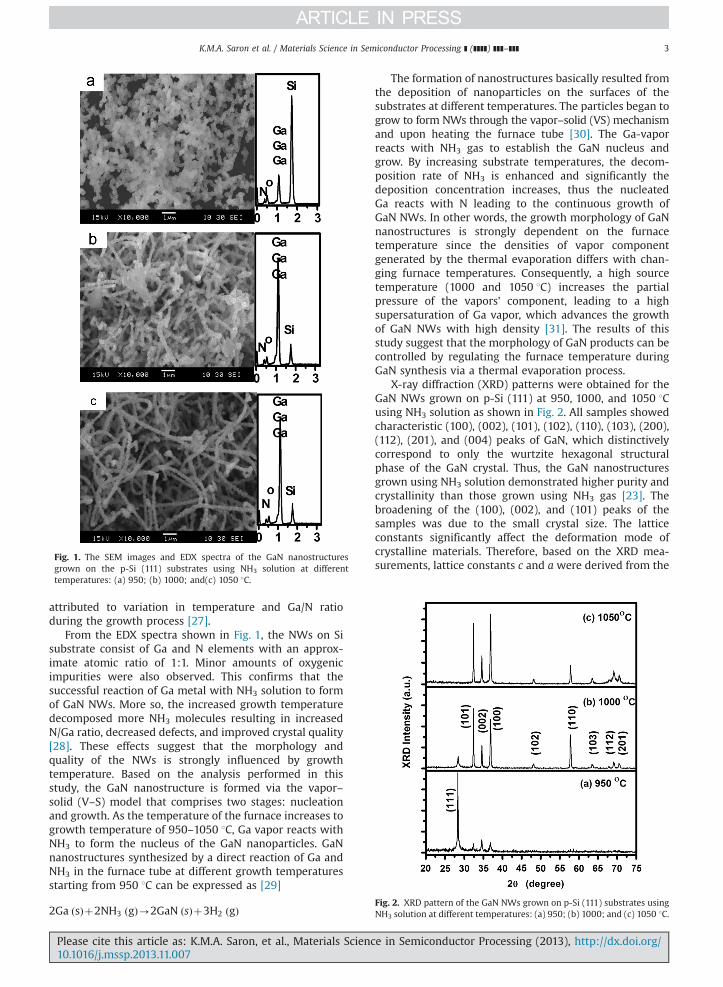
Fig. 1. The SEM images and EDX spectra of the GaN nanostructuresgrown on the p-Si (111) substrates using NH3 solution at differenttemperatures: (a) 950; (b) 1000; and(c) 1050 1C.
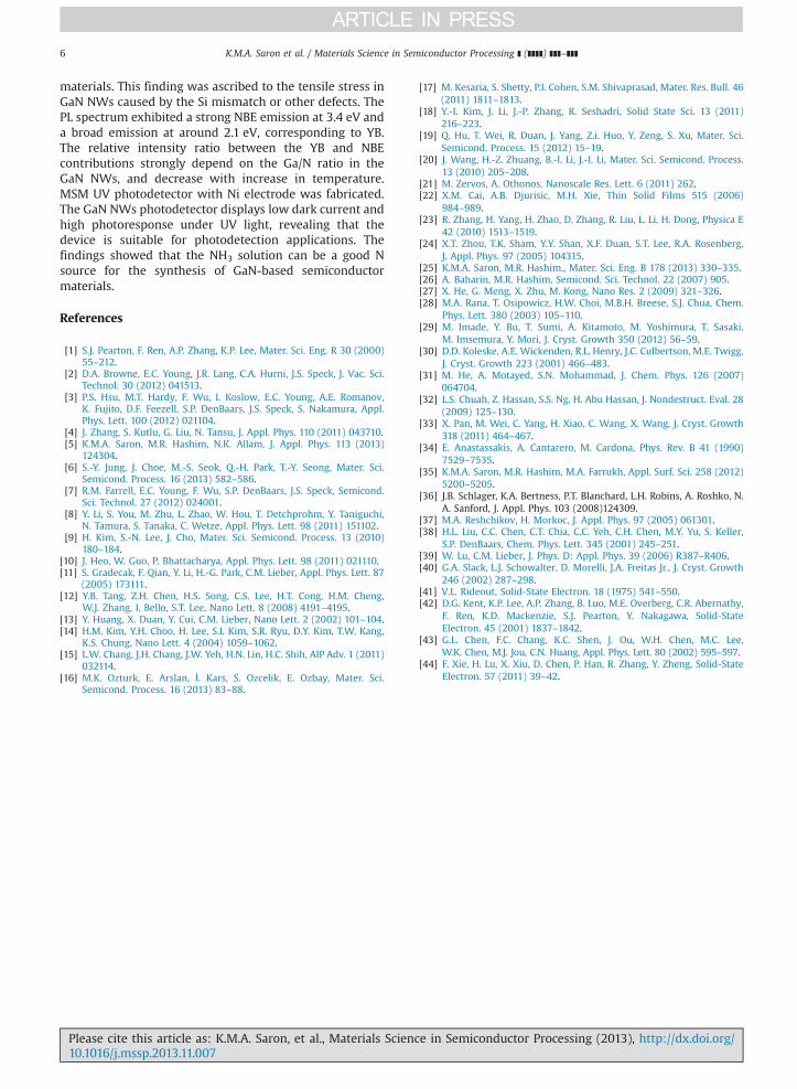
Fig. 2. XRD pattern of the GaN NWs grown on p-Si (111) substrates usingNH3 solution at different temperatures: (a) 950; (b) 1000; and (c) 1050 1C.
K.M.A. Saron et al. / Materials Science in Semiconductor Processing ] (]]]]) ]]]–]]] 3
attributed to variation in temperature and Ga/N ratioduring the growth process [27].
From the EDX spectra shown in Fig. 1, the NWs on Sisubstrate consist of Ga and N elements with an approx-imate atomic ratio of 1:1. Minor amounts of oxygenicimpurities were also observed. This confirms that thesuccessful reaction of Ga metal with NH3 solution to formof GaN NWs. More so, the increased growth temperaturedecomposed more NH3 molecules resulting in increasedN/Ga ratio, decreased defects, and improved crystal quality[28]. These effects suggest that the morphology andquality of the NWs is strongly influenced by growthtemperature. Based on the analysis performed in thisstudy, the GaN nanostructure is formed via the vapor–solid (V–S) model that comprises two stages: nucleationand growth. As the temperature of the furnace increases togrowth temperature of 950–1050 1C, Ga vapor reacts withNH3 to form the nucleus of the GaN nanoparticles. GaNnanostructures synthesized by a direct reaction of Ga andNH3 in the furnace tube at different growth temperaturesstarting from 950 1C can be expressed as [29]
2Ga ðsÞþ2NH3 ðgÞ-2GaN ðsÞþ3H2 ðgÞ
Please cite this article as: K.M.A. Saron, et al., Materials Scienc10.1016/j.mssp.2013.11.007i
The formation of nanostructures basically resulted fromthe deposition of nanoparticles on the surfaces of thesubstrates at different temperatures. The particles began togrow to form NWs through the vapor–solid (VS) mechanismand upon heating the furnace tube [30]. The Ga-vaporreacts with NH3 gas to establish the GaN nucleus andgrow. By increasing substrate temperatures, the decom-position rate of NH3 is enhanced and significantly thedeposition concentration increases, thus the nucleatedGa reacts with N leading to the continuous growth ofGaN NWs. In other words, the growth morphology of GaNnanostructures is strongly dependent on the furnacetemperature since the densities of vapor componentgenerated by the thermal evaporation differs with chan-ging furnace temperatures. Consequently, a high sourcetemperature (1000 and 1050 1C) increases the partialpressure of the vapors' component, leading to a highsupersaturation of Ga vapor, which advances the growthof GaN NWs with high density [31]. The results of thisstudy suggest that the morphology of GaN products can becontrolled by regulating the furnace temperature duringGaN synthesis via a thermal evaporation process.
X-ray diffraction (XRD) patterns were obtained for theGaN NWs grown on p-Si (111) at 950, 1000, and 1050 1Cusing NH3 solution as shown in Fig. 2. All samples showedcharacteristic (100), (002), (101), (102), (110), (103), (200),(112), (201), and (004) peaks of GaN, which distinctivelycorrespond to only the wurtzite hexagonal structuralphase of the GaN crystal. Thus, the GaN nanostructuresgrown using NH3 solution demonstrated higher purity andcrystallinity than those grown using NH3 gas [23]. Thebroadening of the (100), (002), and (101) peaks of thesamples was due to the small crystal size. The latticeconstants significantly affect the deformation mode ofcrystalline materials. Therefore, based on the XRD mea-surements, lattice constants c and a were derived from the
e in Semiconductor Processing (2013), http://dx.doi.org/

Fig. 3. Raman spectra of the NWs grown on the Si substrates at differenttemperatures: (a) 950; (b) 1000; and (c) 1050 1C.
Fig. 4. The figure shows PL emission spectrum GaN NWs grown on p-Si(111) at different temperatures: (a) 950; (b) 1000; and 1050 1C.
K.M.A. Saron et al. / Materials Science in Semiconductor Processing ] (]]]]) ]]]–]]]4
peak position of (002) and (110) planes, respectively [32].The calculated lattice constants were a¼3.182 Å andc¼5.179 Å for Samples a and b, as well as a¼3.187 Å andc¼5.184 Å for sample c. These results are consistent withthe standard values listed in JCPDS card no. 076-0703. TheXRD measurements confirmed that the synthesized GaNNWs have proper crystal qualities.
The Raman spectra were obtained for NWs grown on Si(111) substrate under different growth temperatures asshown in Fig. 3. The peak observed around 519 cm�1
represents the Si substrate. The E2-high and A1-(LO) modesof GaN in this study are consistent with earlier reports[23,33]. The E2 (high) peaks of the samples were red shifted,as shown in Fig. 3. A comparison between the standardfrequency value of E2 (high) phonon (568 cm�1) for bulkGaN [33] and the peak positions of the E2 (high) phononmode obtained in this study indicate a major shift towardsthe lower frequencies by about 3.0, 1.7, and 1.2 cm�1. Thedownward shifts in the position of E2 (high) phonon modeindicate that the GaN nanostructures are affected byreduced tensile stress as a result of increased temperature.Based on a study by Anastassakis et al. [34], the stress levelsof the GaN epilayer and the Raman shift are given by theequation; Δω¼4.3sxx.The biaxial tensile stresses (sxx) wascalculated from the variation in wave number (Δω) of E2(high) mode to be 0.7, 0.4, and 0.28 GPa for the samplesgrown at 950, 1000, and 1050 1C, respectively.
The Raman spectra indicate that the tensile stressdecreases with rise in temperature. With increasing tem-peratures, the decomposition NH3 increase, which result inimproved crystalline quality and reduced stress in nanos-tructures. Sample a exhibited the highest stress, suggestingthat reduced temperature led to increased stress because ofdefects from vacancies, and lattice distortion [35]. The peaksaround 730 cm�1 are associated with the A1 (LO) mode,while the peak at 416 cm�1 corresponds to the acousticovertone mode in single-crystal wurtzite GaN.
Furthermore, RT photoluminescence (PL) spectra wereacquired for GaN nanostructures synthesized at differenttemperatures in this study as shown in Fig. 4. All thesamples exhibited a near band-edge (NBE) emission at
Please cite this article as: K.M.A. Saron, et al., Materials Scienc10.1016/j.mssp.2013.11.007i
around 363–368 nm. The observed peaks are in agrees withthe experimental bandgap value of the bulk GaN (364 nm).The spectra indicate that peak intensities increase withgrowth temperatures. Nanostructures obtained at 950 1Cexhibited NBE emission peak at 368 nm (3.37 eV) and abroad yellow band (YB) emission at 557 nm. The samplegrown at 1000 1C shows a strong NBE at approximately367 nm (3.38 eV) and a weak YB emission peak at 556 nm.The strong UV emission ranging from 363 nm to 368 nmresults from the recombination of free excitons [36]. The YBemissions associated to the deep level states related to low-concentration defects such as gallium or nitrogen vacancies(VGa or VN) [37]. The GaN NWs grown at 1050 1C exhibitsthe strongest NBE emission intensity at 363.7 nm (3.4 eV).However, no peak was identified with blue or yellowemission (BE, YE), which indicates the sample c is of highoptical quality. Increasing temperatures seem to suppressthe YB emission peak. Decreasing in the intensity of YBpeaks indicates that the concentration defect decreaseswith growth temperature. Increase in growth temperaturestrongly affected the Ga/N reactant ratio in the system,leading to morphological variations and improved crystalquality of the NWs [38]. The broadening of visible emissionin the PL spectra of GaN nanostructures indicates thepresence of heterogeneous strains [39]. As temperatureincreases, the NBE peak intensity increases while YB emis-sion decreases significantly, which suggests enhanced opticalquality of the GaN NWswith temperature. The FWHM valuesof NBE peaks in the PL spectra were 15.2, 12.6 and 5.9 nm forsamples a, b, and c respectively. The FWHM values decreasedwith increasing growth temperature. The high quality opticalproperties exhibited by GaN NWs synthesized in NH3 solu-tion can be attributed to inhibition of vacancy developmentand improved NW crystallinity. Based on the PL emissionsand FWHM values, the optimum temperature for GaNsynthesis is 1050 1C.
The tope surface of GaN NWs was deposited by Nimetal to produce MSM photodetector. Most importantly, itmust first be noted that epitaxial nanowires due to theirhorizontal alignment are very easily integrated with con-tact electrodes. The GaN NWs are expected to be has anintrinsic n-type conductivity behaviors because of oxygentraces in the tube furnace which it may become a dopant
e in Semiconductor Processing (2013), http://dx.doi.org/

Fig. 5. (A) I–V characteristics of the fabricated NWs MSM UV photo-detectors measured in dark and under (365 nm) illumination and (B) thecontrast ratio of GaN NWs synthesized at 1050 1C, the inset is schematicof the Ni/GaN NWs/Ni MSM photodetector.
K.M.A. Saron et al. / Materials Science in Semiconductor Processing ] (]]]]) ]]]–]]] 5
source during the growth process [40]. Fig. 5(a) showscurrent–voltage (I–V) characteristics of the MSM photo-detector (sample 1050 1C) with Ni electrodes measured indark and under illumination (365 nm). It can be seen thatthe photocurrent of the fabricated Schottky diode isobviously higher than the dark current. In dark I–V, thebarrier heights and ideality factors of each Ni/GaNSchottky diode were determined. It was found that theseI–V curves can be fitted well by the thermionic emissiontheory as follows [41]:
I¼ I0 expqVnkT
� ��1
� �ð1Þ
where V is the voltage across the diode, n is the idealityfactor, k is the Boltzman constant and I0 is the saturationcurrent given by
I0 ¼ AAnnT2exp�qφB0
kT
h ið2Þ
where q is the electron charge, T is the temperature in K,A is the contact area, Ann is the effective Richardson constantand φB0 is the Schottky barrier height. From the forwardlog I–V curve, the ideality factors n, Schottky barrier
Please cite this article as: K.M.A. Saron, et al., Materials Scienc10.1016/j.mssp.2013.11.007i
heights φB0, and saturation current I0 of this diode can beobtained. The calculated values of ideality factor andbarrier height of the Ni on n-GaN NWs photodetectorwere, 2.1, and 0.73 eV, respectively. The saturation currentwas found to be I0¼1.37�10�7 A. A high value of idealityfactor can be attributed to an increased the resistivity ofNi/n-GaN at the interface due to the low annealingtemperature of the junction [42]. The large value ofideality factor can also be as a result of the increasedresistivity of Ni/n-GaN at the interface due to the surfacerough of NWs. The obtained barrier height value is con-sistent with usually reported values for Ni/n-GaN diode[43]. The large barrier height causes small current leakage,which increases the photocurrent to dark currentcontrast ratio.
Fig. 5(a) shows the non-linear I–V characteristics of Nicontact on the as grown GaN NWs, which are suggestive ofthe Schottky contact between the GaN NWs and Nielectrode. The dark current and photocurrent of thefabricated MSM photodetector at applied bias of þ5 Vwere estimated to be 14.8 mA and 1.6 mA, respectively.Under UV light, the photocurrent of MSM was found to betwo orders higher in magnitude than the dark current,because of the large volume of photon generated carriersand the high absorption of most incident photons by theGaN NWs. A high photocurrent could also be attributed tolight-induced electron-hole generation at the depletionarea of the GaN NWs, particularly near the heterostructureinterface when light is conducted into the NWs, and thegeneration of more electrons between semiconductors andmetals [44]. This result indicates high photo response ofthe NWs.
Contrast ratio (sensitivity) is an important factor formeasuring the viability of a UV detector. Contrast ratio isdefined as the ratio of photocurrent (Iph) to dark current(Id) i.e., (Iph/Id). Fig. 5(b) shows the contrast ratio of theGaN NWs based MSM UV photodetectors with Ni andindicating a high contrast ratio of 120. The current gain forthe sample is consistent with the PL results, wherebysample with the highest UV spontaneous emission show-ing high current gain for UV detection. The tremendousresponse under UV light could be attributed by the zigzagnature of the sample which enhancing the absorption ofthe incident photon. The high sensitivity of the NWs mightalso be attributed to the low lattice scattering and highcarrier mobility in this Ni/n-GaN MSM photodetector.
4. Conclusion
GaN NWs were successfully synthesized on p-Si (111)substrate by the direct reaction of Ga vapor with gaseousNH3 under nitrogen flow rate at different growth tem-peratures of 950, 1000, and 1050 1C. The presence of NH3
solution and temperature significantly influenced thegrowth, structure, and optical properties of NWs. TheNW density increased with increase in temperature. XRDmeasurements revealed that all diffraction peaks corre-spond to wurtzite hexagonal structure of the GaN crystal.NW crystallinity improved with increase in temperature.The Raman spectra of the GaN NWs demonstrated a redshift in the E2 (high) peak compared with the perfect bulk
e in Semiconductor Processing (2013), http://dx.doi.org/
K.M.A. Saron et al. / Materials Science in Semiconductor Processing ] (]]]]) ]]]–]]]6
materials. This finding was ascribed to the tensile stress inGaN NWs caused by the Si mismatch or other defects. ThePL spectrum exhibited a strong NBE emission at 3.4 eV anda broad emission at around 2.1 eV, corresponding to YB.The relative intensity ratio between the YB and NBEcontributions strongly depend on the Ga/N ratio in theGaN NWs, and decrease with increase in temperature.MSM UV photodetector with Ni electrode was fabricated.The GaN NWs photodetector displays low dark current andhigh photoresponse under UV light, revealing that thedevice is suitable for photodetection applications. Thefindings showed that the NH3 solution can be a good Nsource for the synthesis of GaN-based semiconductormaterials.
References
[1] S.J. Pearton, F. Ren, A.P. Zhang, K.P. Lee, Mater. Sci. Eng. R 30 (2000)55–212.
[2] D.A. Browne, E.C. Young, J.R. Lang, C.A. Hurni, J.S. Speck, J. Vac. Sci.Technol. 30 (2012) 041513.
[3] P.S. Hsu, M.T. Hardy, F. Wu, I. Koslow, E.C. Young, A.E. Romanov,K. Fujito, D.F. Feezell, S.P. DenBaars, J.S. Speck, S. Nakamura, Appl.Phys. Lett. 100 (2012) 021104.
[4] J. Zhang, S. Kutlu, G. Liu, N. Tansu, J. Appl. Phys. 110 (2011) 043710.[5] K.M.A. Saron, M.R. Hashim, N.K. Allam, J. Appl. Phys. 113 (2013)
124304.[6] S.-Y. Jung, J. Choe, M.-S. Seok, Q.-H. Park, T.-Y. Seong, Mater. Sci.
Semicond. Process. 16 (2013) 582–586.[7] R.M. Farrell, E.C. Young, F. Wu, S.P. DenBaars, J.S. Speck, Semicond.
Sci. Technol. 27 (2012) 024001.[8] Y. Li, S. You, M. Zhu, L. Zhao, W. Hou, T. Detchprohm, Y. Taniguchi,
N. Tamura, S. Tanaka, C. Wetze, Appl. Phys. Lett. 98 (2011) 151102.[9] H. Kim, S.-N. Lee, J. Cho, Mater. Sci. Semicond. Process. 13 (2010)
180–184.[10] J. Heo, W. Guo, P. Bhattacharya, Appl. Phys. Lett. 98 (2011) 021110.[11] S. Gradecak, F. Qian, Y. Li, H.-G. Park, C.M. Lieber, Appl. Phys. Lett. 87
(2005) 173111.[12] Y.B. Tang, Z.H. Chen, H.S. Song, C.S. Lee, H.T. Cong, H.M. Cheng,
W.J. Zhang, I. Bello, S.T. Lee, Nano Lett. 8 (2008) 4191–4195.[13] Y. Huang, X. Duan, Y. Cui, C.M. Lieber, Nano Lett. 2 (2002) 101–104.[14] H.M. Kim, Y.H. Choo, H. Lee, S.I. Kim, S.R. Ryu, D.Y. Kim, T.W. Kang,
K.S. Chung, Nano Lett. 4 (2004) 1059–1062.[15] L.W. Chang, J.H. Chang, J.W. Yeh, H.N. Lin, H.C. Shih, AIP Adv. 1 (2011)
032114.[16] M.K. Ozturk, E. Arslan, İ. Kars, S. Ozcelik, E. Ozbay, Mater. Sci.
Semicond. Process. 16 (2013) 83–88.
Please cite this article as: K.M.A. Saron, et al., Materials Scienc10.1016/j.mssp.2013.11.007i
[17] M. Kesaria, S. Shetty, P.I. Cohen, S.M. Shivaprasad, Mater. Res. Bull. 46(2011) 1811–1813.
[18] Y.-I. Kim, J. Li, J.-P. Zhang, R. Seshadri, Solid State Sci. 13 (2011)216–223.
[19] Q. Hu, T. Wei, R. Duan, J. Yang, Z.i. Huo, Y. Zeng, S. Xu, Mater. Sci.Semicond. Process. 15 (2012) 15–19.
[20] J. Wang, H.-Z. Zhuang, B.-l. Li, J.-l. Li, Mater. Sci. Semicond. Process.13 (2010) 205–208.
[21] M. Zervos, A. Othonos, Nanoscale Res. Lett. 6 (2011) 262.[22] X.M. Cai, A.B. Djurisic, M.H. Xie, Thin Solid Films 515 (2006)
984–989.[23] R. Zhang, H. Yang, H. Zhao, D. Zhang, R. Liu, L. Li, H. Dong, Physica E
42 (2010) 1513–1519.[24] X.T. Zhou, T.K. Sham, Y.Y. Shan, X.F. Duan, S.T. Lee, R.A. Rosenberg,
J. Appl. Phys. 97 (2005) 104315.[25] K.M.A. Saron, M.R. Hashim., Mater. Sci. Eng. B 178 (2013) 330–335.[26] A. Baharin, M.R. Hashim, Semicond. Sci. Technol. 22 (2007) 905.[27] X. He, G. Meng, X. Zhu, M. Kong, Nano Res. 2 (2009) 321–326.[28] M.A. Rana, T. Osipowicz, H.W. Choi, M.B.H. Breese, S.J. Chua, Chem.
Phys. Lett. 380 (2003) 105–110.[29] M. Imade, Y. Bu, T. Sumi, A. Kitamoto, M. Yoshimura, T. Sasaki,
M. Imsemura, Y. Mori, J. Cryst. Growth 350 (2012) 56–59.[30] D.D. Koleske, A.E. Wickenden, R.L. Henry, J.C. Culbertson, M.E. Twigg,
J. Cryst. Growth 223 (2001) 466–483.[31] M. He, A. Motayed, S.N. Mohammad, J. Chem. Phys. 126 (2007)
064704.[32] L.S. Chuah, Z. Hassan, S.S. Ng, H. Abu Hassan, J. Nondestruct. Eval. 28
(2009) 125–130.[33] X. Pan, M. Wei, C. Yang, H. Xiao, C. Wang, X. Wang, J. Cryst. Growth
318 (2011) 464–467.[34] E. Anastassakis, A. Cantarero, M. Cardona, Phys. Rev. B 41 (1990)
7529–7535.[35] K.M.A. Saron, M.R. Hashim, M.A. Farrukh, Appl. Surf. Sci. 258 (2012)
5200–5205.[36] J.B. Schlager, K.A. Bertness, P.T. Blanchard, L.H. Robins, A. Roshko, N.
A. Sanford, J. Appl. Phys. 103 (2008)124309.[37] M.A. Reshchikov, H. Morkoc, J. Appl. Phys. 97 (2005) 061301.[38] H.L. Liu, C.C. Chen, C.T. Chia, C.C. Yeh, C.H. Chen, M.Y. Yu, S. Keller,
S.P. DenBaars, Chem. Phys. Lett. 345 (2001) 245–251.[39] W. Lu, C.M. Lieber, J. Phys. D: Appl. Phys. 39 (2006) R387–R406.[40] G.A. Slack, L.J. Schowalter, D. Morelli, J.A. Freitas Jr., J. Cryst. Growth
246 (2002) 287–298.[41] V.L. Rideout, Solid-State Electron. 18 (1975) 541–550.[42] D.G. Kent, K.P. Lee, A.P. Zhang, B. Luo, M.E. Overberg, C.R. Abernathy,
F. Ren, K.D. Mackenzie, S.J. Pearton, Y. Nakagawa, Solid-StateElectron. 45 (2001) 1837–1842.
[43] G.L. Chen, F.C. Chang, K.C. Shen, J. Ou, W.H. Chen, M.C. Lee,W.K. Chen, M.J. Jou, C.N. Huang, Appl. Phys. Lett. 80 (2002) 595–597.
[44] F. Xie, H. Lu, X. Xiu, D. Chen, P. Han, R. Zhang, Y. Zheng, Solid-StateElectron. 57 (2011) 39–42.
e in Semiconductor Processing (2013), http://dx.doi.org/