Ordered CdS micro/nanostructures on CdSe nanostructures
10
Ordered CdS micro/nanostructures on CdSe nanostructures This article has been downloaded from IOPscience. Please scroll down to see the full text article. 2009 Nanotechnology 20 125601 (http://iopscience.iop.org/0957-4484/20/12/125601) Download details: IP Address: 129.219.247.33 The article was downloaded on 15/09/2010 at 13:35 Please note that terms and conditions apply. View the table of contents for this issue, or go to the journal homepage for more Home Search Collections Journals About Contact us My IOPscience
-
Upload
independent -
Category
Documents
-
view
2 -
download
0
Transcript of Ordered CdS micro/nanostructures on CdSe nanostructures

Ordered CdS micro/nanostructures on CdSe nanostructures
This article has been downloaded from IOPscience. Please scroll down to see the full text article.
2009 Nanotechnology 20 125601
(http://iopscience.iop.org/0957-4484/20/12/125601)
Download details:
IP Address: 129.219.247.33
The article was downloaded on 15/09/2010 at 13:35
Please note that terms and conditions apply.
View the table of contents for this issue, or go to the journal homepage for more
Home Search Collections Journals About Contact us My IOPscience

IOP PUBLISHING NANOTECHNOLOGY
Nanotechnology 20 (2009) 125601 (9pp) doi:10.1088/0957-4484/20/12/125601
Ordered CdS micro/nanostructures onCdSe nanostructuresGuozhang Dai, Zhiwei Peng, Qinglin Zhang1, Weichang Zhou,Mingxia Xia, Hongxing Li, Anlian Pan, Qiang Wan andBingsuo Zou1
State Key Lab of CBSC, and Micro-nano Research Center, Hunan University,Changsha 410082, People’s Republic of China
E-mail: [email protected] and [email protected]
Received 23 September 2008, in final form 30 December 2008Published 4 March 2009Online at stacks.iop.org/Nano/20/125601
AbstractComposite structures of aligned and orientation-ordered quasi-one-dimensional CdSmicro/nanostructures on CdSe substrates of different shaped nanostructures have beensynthesized by using two-step thermal evaporation processes. The CdSe substrate crystallineorientations and local temperatures play their roles in the CdS nanostructure growth step, whichis in some contrast with the vapor–liquid–solid (VLS) growth mechanism.Micro-photoluminescence measurements show strong luminescence responses on the six-foldsymmetrical CdSe/CdS nanostructure. Controllable growth on various shaped substrates mayfind applications in obtaining many other aligned orientation-orderedhetero-nano/microstructure materials.
1. Introduction
Low-dimensional semiconductor materials in the micro/nano-scale have been intensively studied during the past few yearsbecause of their unique properties as well as their potentiallywide applications in electronic, optical, and magneticdevices [1]. Hierarchical semiconductor micro/nanostructures,which consist of a backbone and many branches, have recentlybecome especially attractive as building blocks or for theassembly of integrated multifunctional micro/nanosystems,since those flexible structures or substances provide anadditional approach for increasing the three-dimensional(3D) structural, compositional and functional diversity. Inrecent years, many synthetic methods have been reported forgrowing hierarchical structures [2–5], such as multibranchnanostructures via sequential seeding of catalysts [6].Fabricating hierarchical heterostructures with compositionaland dimensional control of the backbone and branch canachieve specific functionalities due to their heterojunctions,such as co-axial heterojunctions [7] and/or core–shellmicro/nano heterostructures [8]. From these considerationsa lot of works on hierarchical heterostructures have beenreported both in solution [9] and in vapor [10]. Someother specific methods include the template-assisted formation
1 Authors to whom any correspondence should be addressed.
of aligned nanowire arrays [11], self-assembled dendriticgrowth of micro/nanowires [12], and the thermally assistedpulsed laser ablation (TAPLA) process [13]. These methodshave had some success in the formation of hierarchicalheterostructures; however, new growth techniques still needto be developed since many hierarchical heterostructureswith new morphologies, sizes, composition and functions areanticipated.
Very recently, a simple two-step thermal evaporationmethod has been extensively used in the synthesis ofhierarchical heterostructures [14–16]. This method, whichprovides good controllability and versatility in the formationof hierarchical semiconductor heterojunctions, is applied inthis study. The II–VI semiconductor materials CdS (Eg =2.42 eV at room temperature) and CdSe (Eg = 1.74 eVat room temperature) have the same structure and similarproperties [17]. Rational synthesis of CdS and CdSeheterostructures with controlled composition and morphologywill allow for the assembly of complex micro/nanostructuresystems.
In the last few years, a few excellent works on thesynthesis of CdSe/CdS heterostructure systems have beenreported [18, 19] in which most of the products are nanorods ofaxial or core–shell heterostructures, but hierarchical CdSe/CdSheterostructures, to the best of our knowledge, have not beenobtained. In this paper, we report the synthesis of a few
0957-4484/09/125601+09$30.00 © 2009 IOP Publishing Ltd Printed in the UK1

Nanotechnology 20 (2009) 125601 G Dai et al
aligned and orientation-ordered CdS micro/nanostructures onvarious shaped CdSe nanostructures as substrates througha two-step thermal evaporation process. The effects ofCdSe nanostructure morphology and local temperatures onthe CdS growth are significant, which is in contrast to earlypublications. The optical property of the six-fold symmetricalCdSe/CdS structure was studied through near-field opticalmicroscopy (NSOM). The results showed that the CdSe/CdSnanosystem was very sensitive to light at various locations.
2. Experimental procedures
The orientation-ordered CdS/CdSe heterostructures weresynthesized through a two-step catalyst mediated vapor–liquid–solid (VLS) process in a horizontal tube furnace.First, obtaining orientation-ordered arrays is a critical steptoward the goal of micro/nanoscale devices [20–22], somass production of CdSe nanostructures such as nanosheets,nanobelts, and nanowires is achieved by one-step method ofthermal evaporation of CdSe powders onto silicon substrateswith the presence of Au catalyst [23]. In the followingstep, Au catalyst nanoclusters are deposited on the CdSesubstrates via dc sputtering; these serve as the substrates forthe subsequent growth of CdS nanostructures and are placeddownstream from the source material to collect the depositednanostructures. The source material, 0.1 g CdS powder, isplaced at the same position where the CdSe powders stay atthe first step. The temperature at the center of tube is elevatedto 800 ◦C for CdSe (750 ◦C for CdS) at a rate of 100 ◦C min−1.After 60 min (120 min for the longer tapered CdS belts) oftypical deposition for growing CdS, the furnace is cooled downto room temperature. Then the products are taken out forcharacterization. All the growth processes were carried outunder 20–30 sccm Ar (90%)–H2 (10%) mixture carrier gas.
X-ray powder diffraction (XRD) data were obtained on aSiemens D-5000 type diffractometer equipped with graphite-monochromatized Cu Kα radiation (l = 1.5405 A). Themorphologies and structures of the sample structures wereexamined by a field emission scanning electron microscope(SEM, JSM-6700F) and a transmission electron microscope(TEM, JEM-3010). The composition of the samplewas confirmed with energy-dispersive spectrometry (EDS)attached to the SEM. The micro-photoluminescence (micro-PL) measurements were taken on an Alpha SNOM near-fieldoptical microscope (Witec) using an Ar-ion laser (488 nm) asthen excitation light source.
3. Results and discussion
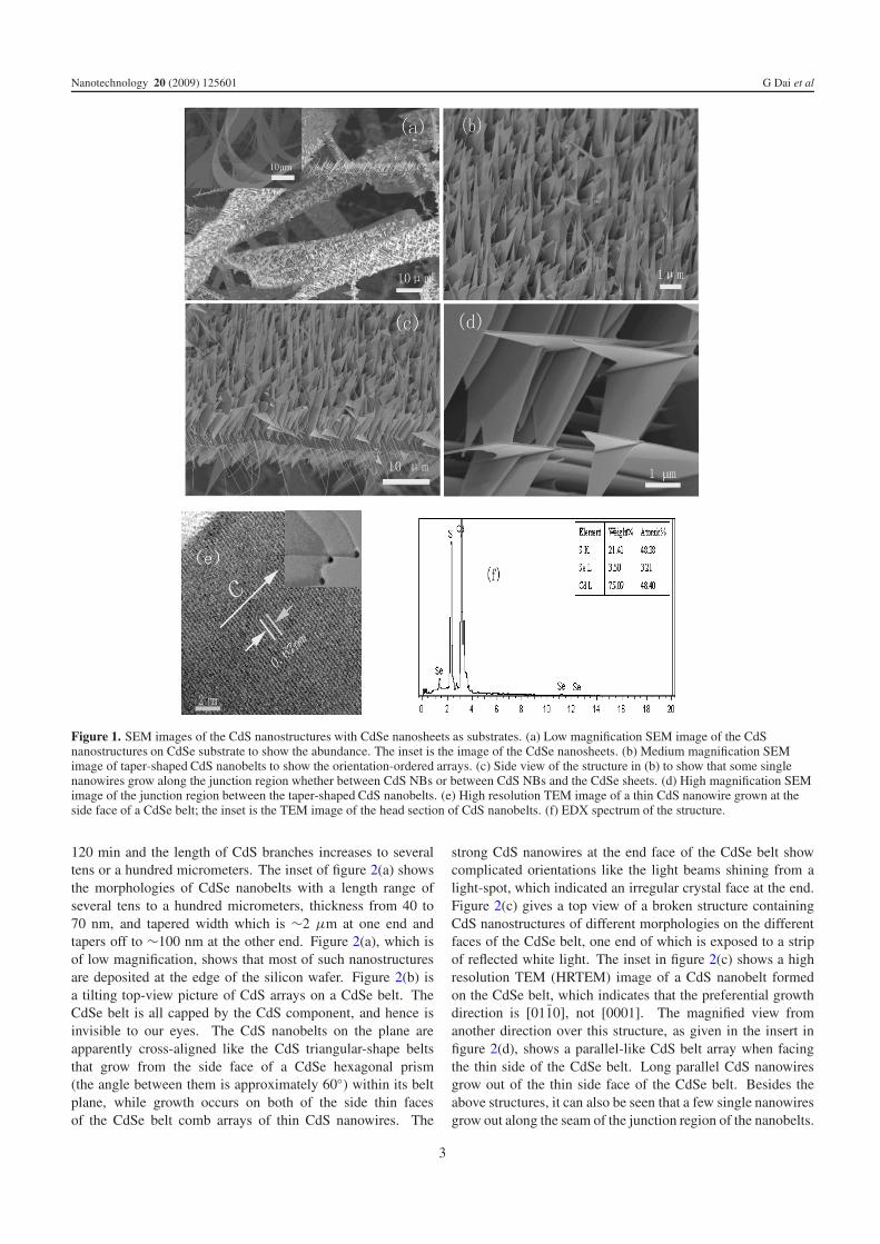
It is well known that in a CdSe belt grown via the VLS growthmechanism, the short axis is along [0001] and the long axis isperpendicular to [0001], and the belt is composed of numerous,parallel and closely connected hexagonal nanowires [3b].Based on the CdSe substrate we expect some regular growthof CdS nanostructures. The morphologies of the sample werecharacterized by SEM observation. Figures 1(a) and (b) showthe typical SEM images of CdS nanostructures at low andmedium magnifications with CdSe nanosheets as the substrate,
respectively. The low magnification image in figure 1(a)shows a large quantity of such nanostructures on the CdSenanosheets. The inset of figure 1(a) is the SEM image ofas-prepared CdSe nanosheets, several tens of micrometers inlength, 5–8 μm in width, and 40–50 nm in thickness, onwhich the later CdS nanostructures grow. Figure 1(b) showsan SEM image of medium magnification in which the laterdeposited components (CdS) are orientationally aligned, andhave a dominant morphology of taper-shaped CdS nanobelts(NBs) whose tapered widths increase gradually along thegrowth axis, starting from the tip region where liquid Aunanoparticle adhere to CdS nanostructures, to the connectionregion between CdS and CdSe. Close examination of thesenanostructures in figures 1(c) and (d) reveals that there existsa defined relationship between the orientation of the CdSnanobelts and the plane of CdSe sheets, with a definite anglebetween them. A number of CdS NBs with parallel alignmentgrow up with an approximately 60◦ angle to the plane or thelong axis of the substrate, with minor exceptions (result 1).Besides the nanobelts it can also be seen from figure 1(c) thatsome very thin nanowires grow along the connection line of theCdS belts and CdSe sheet. Such single nanowire grow becausethe connection regions between every two belts are line-shapedand this extended ‘line’ is an easy growth direction [0001] (seefigure 1(e), result 2). Au catalysts were observed at the ends ofthe taper-shaped CdS nanobelts in figures 1(d) and (e) (result3). These three results seem to reflected different growth habitsfrom those reported previously.
CdS grows due to the Au conduction, i.e. the vapor–liquid–solid (VLS) mechanism. Usually, VLS growth dependslittle on the substrate and the preferential growth direction is[0001]. Here CdS grows into NBs with initiation from thesecondary deposited Au nanoparticles, which should not beaccounted for by the VLS mechanism alone. There clearly isan additional vapor–solid (VS) process [24] for the formationof tapered CdS nanobelts on the CdSe sheet. This can be seenfrom the large width at the initial base and swift decrease ofbelt width with the growth. Apart from the temperature, thesubstrate effects play a significant role in the secondary growth.(1) The growth direction is not [0001]; one-dimensional (1D)growth cannot continue, so two-dimensional (2D) growthdominates, but with different speed. (2) The angle betweenthe CdS belt and CdSe sheet reflects that the CdS grows fromone side face of the hexagonal prism on the sheet. (3) TheCdS tapered belt is grown from a nanowire (001) base at theCdSe sheet, which is in exact agreement with the connectionline orientation between CdS belt and CdSe sheet and extendedCdS nanowire (result 2). This connection region can alsobe confirmed from their XRD patterns. The in situ energy-dispersive x-ray analysis (EDX) (figure 1(e)) proves that thesample contain the elements S, Se, and Cd. The atomic ratioof (S + Se)/Cd is very close to 1 (see the inset of this image),indicating the formation of CdS/CdSe heterostructures. Theabove results clearly indicate that the VLS growth woulddepend on the substrate if their crystal structure is the same.
Figure 2 shows typical SEM images of the orientation-ordered CdS nanostructures on a CdSe nanobelt. The typicaldeposition time for growing CdS nanostructures changes to
2
Nanotechnology 20 (2009) 125601 G Dai et al
Figure 1. SEM images of the CdS nanostructures with CdSe nanosheets as substrates. (a) Low magnification SEM image of the CdSnanostructures on CdSe substrate to show the abundance. The inset is the image of the CdSe nanosheets. (b) Medium magnification SEMimage of taper-shaped CdS nanobelts to show the orientation-ordered arrays. (c) Side view of the structure in (b) to show that some singlenanowires grow along the junction region whether between CdS NBs or between CdS NBs and the CdSe sheets. (d) High magnification SEMimage of the junction region between the taper-shaped CdS nanobelts. (e) High resolution TEM image of a thin CdS nanowire grown at theside face of a CdSe belt; the inset is the TEM image of the head section of CdS nanobelts. (f) EDX spectrum of the structure.
120 min and the length of CdS branches increases to severaltens or a hundred micrometers. The inset of figure 2(a) showsthe morphologies of CdSe nanobelts with a length range ofseveral tens to a hundred micrometers, thickness from 40 to70 nm, and tapered width which is ∼2 μm at one end andtapers off to ∼100 nm at the other end. Figure 2(a), which isof low magnification, shows that most of such nanostructuresare deposited at the edge of the silicon wafer. Figure 2(b) isa tilting top-view picture of CdS arrays on a CdSe belt. TheCdSe belt is all capped by the CdS component, and hence isinvisible to our eyes. The CdS nanobelts on the plane areapparently cross-aligned like the CdS triangular-shape beltsthat grow from the side face of a CdSe hexagonal prism(the angle between them is approximately 60◦) within its beltplane, while growth occurs on both of the side thin facesof the CdSe belt comb arrays of thin CdS nanowires. The
strong CdS nanowires at the end face of the CdSe belt showcomplicated orientations like the light beams shining from alight-spot, which indicated an irregular crystal face at the end.Figure 2(c) gives a top view of a broken structure containingCdS nanostructures of different morphologies on the differentfaces of the CdSe belt, one end of which is exposed to a stripof reflected white light. The inset in figure 2(c) shows a highresolution TEM (HRTEM) image of a CdS nanobelt formedon the CdSe belt, which indicates that the preferential growthdirection is [0110], not [0001]. The magnified view fromanother direction over this structure, as given in the insert infigure 2(d), shows a parallel-like CdS belt array when facingthe thin side of the CdSe belt. Long parallel CdS nanowiresgrow out of the thin side face of the CdSe belt. Besides theabove structures, it can also be seen that a few single nanowiresgrow out along the seam of the junction region of the nanobelts.
3

Nanotechnology 20 (2009) 125601 G Dai et al
Figure 2. (a) Low magnification SEM image of the CdS nanostructures with CdSe nanobelts as substrates. The inset is an image of the CdSenanobelts. (b) A side view of single freestanding CdS array sample. (c) A top view of the other single CdS structure to show the differentsymmetrical structure on the two sides along the transverse and longitudinal directions of the nanobelt; the inset is the HRTEM image at theside edge of the CdS nanobelt. (d) Magnified top view of the nanobelts presenting their parallelogram-like cross section. (e) A top view of thewell-aligned CdS wire-shape arrays. (f) Magnified side view of the wire array with parallel orientation.
These different structures indicated that the preformed CdSebelts with different crystal orientation influence the subsequentCdS growth.
If the temperature in the furnace tube center is reducedto 750 ◦C or below and the other conditions are kept constant,similar orientation-ordered CdS nanowire (NW) arrays (but notnanobelts) could be obtained. Figures 2(e) and (f) show atop view and a side view of well-aligned CdS nanowire arraysgrown on the CdSe belt, respectively. As indicated above, as-formed long CdS NWs grow along a direction at a certain angleto the plane of the CdSe substrates, and get across each otheras from neighboring parallel hexagonal prism arrises. Theirprojections on the substrate plane are all parallel to the longaxis of the substrate. There are also a lot of short nanowiresthat grow along the seam of the joint section between longCdS NWs or between the connection region of long CdS NWsand CdSe NB substrates, as in high temperature growth. Theseshort CdS nanowires all seem to grow parallel to the [0001]direction of the CdSe belt plane (like in figure 1(e)). Thisphenomenon indirectly reflected the lattice orientation of the
long CdS nanowires and the substrate, which is evidenced bythe HRTEM image of a broken junction of CdS/CdSe at anearly stage (about 10 min) which shows that CdS grows mainlyalong the [100] direction. The magnified side view of the longwire arrays in figure 2(f) shows their parallel array and almostequal spacing, which leaves regular spatial channels for light orgas. This kind of highly ordered nanowire array may be usefulfor making a nanowire 3D photonic crystal on a CdSe plate.
Because the second VLS and accompanied VS growth relyon the lattice face which they initiate to grow, to some extent,the above results indicate that the surface of the CdSe beltprobably has some regular fluctuation and is not absolutelysmooth, like a lot of well separated ridges, which go in the[0001] direction. They lead to the formation of almost crossednanowires on the opposite sides of one ridge. This structuralcharacter could easily be found in the CdSe nanobelts [3b], butusually not in the CdS nanobelts and ZnS nanowires. Anothereffect for such growth may come from the sparsely dispersedAu nanocrystals on the surface of the CdSe belt, which initiatethe growth of CdS, but do not determine the growth direction.
4

Nanotechnology 20 (2009) 125601 G Dai et al
Figure 3. SEM image of sixfold arrays of tapered CdS belts around a central CdSe nanowire or microrod backbone. (a) Low magnificationSEM image of the six-fold symmetrical CdS nanostructures. (b) Medium magnification SEM image of taper-shaped CdS nanobelts to showthe sixfold symmetrical array. (c) Low magnification SEM image of the six-fold symmetrical CdS nanostructures with CdSe microrods assubstrates. The inset is an image of the CdSe microrods. (d) and (e) Magnified top views of the orientation-ordered CdS nanobelts on CdSemicrorods with different diameter. (e) A top view of the well-aligned CdS wire-shape arrays. (f) EDX spectrum of the sixfold symmetricalstructure.
The lattice orientation where the Au particle stays determinesthe growth direction.
Figure 3 shows a sixfold array of parallel tapered CdSbelts around the central CdSe rod backbone which forma micro-‘propeller’ as indicated by Gao and Wang [25].Figures 3(a) and (b) show typical SEM images of the six-fold symmetrical propeller structures at low and mediummagnifications, respectively. The low magnification image infigure 3(a) shows a large quantity of such structures. Themedium magnification image in figure 3(b) clearly shows thatthere are different symmetries even in a single structure. (Thedefinition of the symmetry symbols is shown in [10].) Whenthe CdS belts are perpendicular to the backbone of the CdSenanowire and grow in single or multiple faces in two oppositedirections (symbols 1 and 2), we define this symmetry as Sor M for a single wire or multiwire, respectively. Thus, 6Sand 6M symmetry may exist in the CdSe microwire backbone.When the main backbone is large enough (inset in figure 3(c)),multiple faces of secondary belts form on the CdSe rods, asshown in figures 3(c)–(e). Furthermore, it can be seen from the
contrasting results in the medium magnification SEM imagesof figures 3(d) and (e) that the thicker the CdSe backbone(figure 3(d)), the more layers of the secondary CdS belts canform. The CdS belts all grow on the six-fold side-facets ofCdSe rod backbones with suitable diameter. Certainly, we canexpect that most of such structures grow in a single row six-fold symmetry (6S symmetry) when the backbone CdSe wireis a typical hexaprism of definite thickness. The reason theygrow with six-fold symmetry is that the hexagonal wurtzitecrystal face of CdSe can direct the growth of the secondaryCdS branch. The detailed six-fold symmetrical growth processwill be discussed later. The in situ EDX analysis shown infigure 3(f) proves that the sample only contains the elementsS, Se, and Cd, which confirms the formation of a CdS/CdSestructure.
The composition and the crystallographic phase of thesample were obtained by x-ray powder diffraction (XRD).Figure 4 shows the normalized XRD pattern of the CdSe belt,CdS nanowire, and CdSe/CdS sample, respectively. We cansee that all diffraction peaks in each sample can be indexed
5

Nanotechnology 20 (2009) 125601 G Dai et al
2 theta (degree)
Inte
nsity
(a.
u.)
Figure 4. The normalized x-ray diffraction patterns of differentsamples. Curves (a), (b) and (c) are for CdSe, CdS, and CdSe/CdS,respectively.
to typical hexagonal wurtzite crystals. The lattice constants(a = 4.299 A, c = 7.01 A and a = 4.136 A, c = 6.713 A)are in agreement with the values of the standard cards (JCPDS77-21 for CdSe and JCPDS 77-2306 of CdS), respectively.As regards the XRD pattern of the CdSe/CdS sample, thediffraction peaks of both CdSe (+) and CdS (×) are obtained.Most diffraction peaks of the sample are assigned to CdS apartfrom the two strongest ((002) and (100)) peaks of CdSe. It isnoted that the CdS component in the CdS/CdSe system favorsthe (002) peak, which is in agreement with the SEM and TEMobservations. The EDS data indicate that the atomic contentof S is ten times that for Se for the principal component ofCdS. The other two peaks marked by ‘∗’ may originate fromthe naked SiO2 (JCPDS 14-260) on the surface of the siliconwafer.
Why can such highly orientation-ordered CdS nanostruc-tures grow on the CdSe nanostructures? Both their structuresand the formation conditions of the CdSe/CdS heterostructureplay their roles in this fabrication. The HRTEM images (infigures 5(a)–(d)) and selected area electron diffraction (SAED)patterns provided the microscopic structure of final products.Figure 5(a) is a typical TEM image of a straight CdSe nanowireof ∼200 nm thickness. Au catalyst was observed at the endof the nanowire, confirming the VLS growth. Figure 5(b)shows its HRTEM image, demonstrating its lattice orientation.It reveals fringe contrast consistent with (0002) planes andthe growth of the CdSe nanowire along the [0001] direction.The SAED pattern (figure 5(b), inset) also verifies the single-crystalline hexagonal wurtzite structure and a growth directionof the CdSe nanowire along [0001]. A TEM image forthe CdSe belt is hard to obtain for a thick belt; see [24].For a CdS nanobelt on a CdSe belt, the TEM images areshown in figures 5(c) and (d). Figure 5(c) shows the widthof the CdS nanobelt to be ∼500 nm. The HRTEM image(figure 5(d)) reveals its single-crystalline structure and latticeorientation. The SAED pattern (figure 5(d), inset) indicatesthat the nanobelt has a wurtzite structure, and grows along[1010]. The growth direction was also confirmed in figure 5(d),
and the measured lattice spacing of 0.358 nm corresponds tothe spacing between (1010) planes, as known from bulk CdSsamples.
The structural analysis discussed above provides mean-ingful insights into the mechanism of the orientation-orderedCdS growth on the different CdSe nanostructures. The latergrowth CdS nanostructures have the same lattice orientationas that of the substrate. Let us start from the CdSe nanowiresubstrate. The orientation relationships between the backboneand the branched CdS nanobelts are obtained from the SAEDpatterns shown in the inset of figures 5(b) and (d) for thesix-fold symmetry. When the CdSe nanowire is along the[0001] direction, the backbone nanowire is enclosed by {0110}facets, which are six crystallographically equivalent planes.CdS nanobelts grow on each facet of the CdSe nanowire,as shown in figure 6(a). In this case, all the side-branchedCdS nanobelts (long axis [1010]) grow perpendicular to thebackbone (long axis [0001]). Due to the equivalence of thesix directions ±[1010], ±[0110], and ±[1100], the anglesbetween the two adjacent growth directions is 60◦, resultingin the six-fold symmetric distribution of nanobelts aroundthe backbone, as shown in figure 3. As regards the CdSebelt/sheet backbones, the situations are some different andcomplicated. The preferential growth direction (long length)of CdSe nanobelts was along [0110] at higher temperature;however, [0001] was the intrinsic and original preferentialgrowth direction (along the width of the belt) [17d]. Theexperiment indicates that a CdSe belt can be considered asinnumerable parallel CdSe single nanowires which grow along[0001] and are connected (with one facet to each other) alongthe [0110] direction with occasional structural irregularity [3b],so its surface is not smooth but of regular fluctuation or arris–valley–arris–valley structure. Thus the two upward facets andtwo downward facets of the six equivalent crystallographicplanes ±(1000) and ±(1100) in one nanowire were exposedto develop the CdS nanostructure with 60◦. Growth in thedirection perpendicular to the belt plane is not applicable. Thisgrowth diagram can be clearly seen in figures 2(b) and (c). Ifthere are fluctuations on the CdSe belt surface, their involvingangle may be other values (as shown in figures 1(c) and 2(e))for various facets. Concerning those thin CdS nanowires thatgrew out of the side face of the connection region, whetherbetween CdS NBs or between the CdS NB and the CdSe sheet,their occurrence is due to the coincidence of the favored growthdirection [0001] for CdS and CdSe. Their limited sizes shouldbe related to their real growth without catalyst assistance. Thesize of the connection region also limited the diameter of thesenanowires.
The dimension of the CdSe substrate in the CdS/CdSestructures became bigger than the CdSe nanostructuresachieved by the one-step method of thermal evaporation,especially for the wire/rod-shaped backbone. The secondarygrowth may cause a thick CdS1−x Sex shell on the surfaceregion. This is an unavoidable phenomenon in the secondarygrowth [1f].
Micro-PL measurements were conducted on the six-fold symmetrical propeller CdS/CdSe structure. Figures 7(a)and (b) show the emission images for the excitation spot
6

Nanotechnology 20 (2009) 125601 G Dai et al
Figure 5. (a) TEM image of a CdSe nanowire. (b) HRTEM image of a CdSe nanowire and its SAED pattern (inset). (c) TEM image of a CdSnanobelt. (d) HRTEM image of a CdS nanobelt on a CdSe nanobelt and its SAED pattern (inset).
Figure 6. Schematic growth process of orientation-ordered CdS belts with CdSe as substrate.
(488 nm) on the CdS belt branch on a CdSe nanowire and aCdSe wire backbone, respectively. It can be seen in figure 7(a)that the belt branch produces a strong green emission peak at∼510 nm, which was associated to the band-edge emission ofCdS nanobelts [17b]. The emission can transport to the end ofthe CdS belt. Orange emission appears when the laser beamilluminates the axial center of the CdSe nanowire where the
CdS nanobelts are circumvented. Figure 7(c) demonstrates thecorresponding emission peak at ∼586 nm, which is consistentwith the near-band-edge PL of CdS0.66Se0.34 nanobelts [26]. Arelatively weak emission peak can also be found at ∼510 nm,besides this emission. This should be partial excitation of theCdS nanowire close to the junction. Here, the existence of theCdS1−xSex shell confirms the alloy formation in the growth
7

Nanotechnology 20 (2009) 125601 G Dai et al
Figure 7. (a) and (b) Emission images for excited light illuminated on the branch and the backbone, respectively. The inset is the far-fieldoptical image and the red circle denotes the excitation location. (c) Room temperature micro-PL spectrum showing the observed emission in(a) and (b). λexc in (a) and (b) was 488 nm from an Ar+ laser.
(This figure is in colour only in the electronic version)
process of CdS/CdSe structure. Furthermore, it can be seenfrom the emission images that both the branched belt and theaxial wire can exhibit good photoluminescence. Combinedwith the highly orientation-ordered structure, such CdS/CdSesystems may find many applications in photonic devices andsolar cells.
4. Conclusions
In conclusion, aligned and orientation-ordered CdS multi-branch microstructures and nanostructures on various shapedCdSe substrates were obtained through a two-step thermalevaporation process. The structure and growth processesof different CdSe/CdS systems were presented. The latticeorientation of the CdSe substrates determines the growthdirection of the CdS nanostructures, which is in contrast tothe situation in previous VLS growth. The effects of localtemperatures on the growth were also discussed. Micro-PL measurements exhibited their efficient photoluminescencefrom different areas. Such different orientation-ordered CdSmicrostructures and nanostructures as reported here may findpotential applications in a variety of fields such as lumines-cence, solar cells, nanophotonic crystals, nanogenerators, andother photonic devices.
Acknowledgments
We are grateful to the NSFC of China (Term Nos 90606001,20873039 and 90406024), and Hunan youth fund (07jj4002)for financial support.
References
[1a] Alivisatos A P 1996 Science 271 933[1b] Pan Z W, Dai Z R and Wang Z L 2001 Science 291 1947[1c] Peng X, Manna U, Yang W, Wickham J, Scher E,
Kadavanich A and Alivisatos A P 2000 Nature 404 59[1d] Lieber C M 2003 MRS Bull. 28 486[1e] Xia Y, Yang P, Sun Y, Wu Y, Mayers B, Gates B, Yin Y,
Kim F and Yan H 2003 Adv. Mater. 15 353[1f] Pan A, Yang H, Liu R, Yu R, Zou B and Wang Z L 2005
J. Am. Chem. Soc. 127 15692[2] Yan H, He R, Johnson J, Law M, Saykally R J and
Yang P 2003 J. Am. Chem. Soc. 125 4728[3a] Zhou J, Ding Y, Deng S Z, Gong L, Xu N S and Wang Z L
2005 Adv. Mater. 17 2107[3b] Ding Y, Ma Ch and Wang Z L 2004 Adv. Mater. 16 1740[4] May S J, Zheng J G, Wessels B W and Lauhon L J 2005
Adv. Mater. 17 598[5] Wang Q Q, Xu G and Han G R 2006 Cryst. Growth Des.
6 1776[6] Wang D, Qian F, Yang C, Zhong Z H and Lieber C M 2004
Nano Lett. 4 871[7] Gudiksen M S, Lauhon L J, Wang J, Smith D and Lieber C M
2002 Nature 415 617Bjork M T, Ohlsson B J, Sass T, Persson A I, Thelander C,
Magnusson M H, Deppert K, Wallenberg L R andSamuelson L 2002 Nano Lett. 2 87
Wu Y, Fan R and Yang P 2002 Nano Lett. 2 83Xue F H, Fei G T, Cui B, Wu P and Zhang L D 2005 J. Am.
Chem. Soc. 127 15348[8] Lauhon L J, Gudiksen M S, Wang D and Lieber C M 2002
Nature 420 57Jiang X C, Xiong Q, Nam S, Qian F, Li Y and Lieber C M
2007 Nano Lett. 10 3214Shen G Z, Chen D and Lee C J 2007 J. Phys. Chem. C
111 5673
8
Nanotechnology 20 (2009) 125601 G Dai et al
[9] Milliron D J, Hughes S M, Cui Y, Manna L, Li J, Wang L Wand Alivisatos A P 2004 Nature 430 190
[10] Lao J Y, Wen J G and Ren Z F 2002 Nano Lett. 2 1287[11] Xu D S, Shi X S, Guo G L, Gui L L and Tang Y Q 2000
J. Phys. Chem. B 104 5061Wu J J and Liu S C 2002 Adv. Mater. 3 215Yang W B, Zhu S F, Zhao B J, Ye J, Ni J, Zhen W B and
Chen X M 2003 Chin. J. Inorg. Chem. 4 366Moore D F, Ding Y and Wang Z L 2004 J. Am. Chem. Soc.
126 14372Fan H J, Fuhrmann B, Scholza R, Syrowatkab F, Dadgarc A,
Krostc A and Zacharias M 2006 J. Cryst. Growth 287 34[12] Yan H, He R, Johnson J, Law M, Saykally R J and Yang P J
2003 Am. Chem. Soc. 125 4728Hu J Q, Bando Y, Zhan J H, Yuan X L, Sekiguchi T and
Golberg D 2005 Adv. Mater. 17 971Sun S H, Meng G W, Zhang G X and Zhang L D 2007 Cryst.
Growth Des. 7 1988[13] Yang R, Chueh Y L, Morber J R, Snyder R, Chou L J and
Wang Z L 2007 Nano Lett. 2 269[14] Jung Y, Ko D K and Agarwal R 2007 Nano Lett. 2 264[15] Dick K A, Deppert K, Larsson M W, Martensson T, Seifert W,
Wallenberg L R and Samuelson L 2004 Nat. Mater. 3 380[16] Lan Z H, Liang C H, Hsu C W, Wu C T, Lin H M, Dhara S,
Chen K H, Chen L C and Chen C C 2004 Adv. Funct.Mater. 14 233
[17a] Pan A L, Liu R B and Zou B S 2006 Appl. Phys. Lett.88 173102
[17b] Pan A L, Liu D, Liu R B, Wang F F, Zhu X and Zou B S 2005Small 1 980
[17c] Agarwal R, Barrelet C J and Lieber C M 2005 Nano Lett.5 917
[17d] Pan A L, Liu R B, Zhang Q L, Wan Q, He P B,Zacharias M and Zou B S 2007 J. Phys. Chem. C111 14253
[18] Ouyang L, Maher K N, Yu C L, McCarty J and Park H 2007J. Am. Chem. Soc. 129 133
[19] Talapin D V, Shevchenko E V, Murray C B, Kornowski A,Forster S and Weller H 2004 J. Am. Chem. Soc. 126 12984
[20] Huang M H, Mao S, Feick H, Yan H, Wu Y, Kind H,Weber E, Russo R and Yang P 2001 Science 292 1897
[21] Whang D, Jin S, Wu Y and Lieber C M 2003 Nano Lett.3 1255
[22] Wang X, Summers C J and Wang Z L 2003 Nano Lett. 3 1315[23] Dai G Z, Peng Z W, Zhou W C, Xia M X, Zhang Q L, Wan Q,
Pan A L and Zou B S 2008 J. Phys. D: Appl. Phys.41 135301
[24] Brenner S S and Sears G W 1956 Acta Mater. 4 268[25] Gao P X and Wang Z L 2004 Appl. Phys. Lett. 84 2883[26] Liu Y K, Zapien J A, Shan Y Y, Tang H, Lee C S and Lee S T
2007 Nanotechnology 18 365606
9