Electronic transport in films of colloidal CdSe nanocrystals
11
arXiv:cond-mat/0204560v1 [cond-mat.mes-hall] 25 Apr 2002 Electronic transport in films of colloidal CdSe nanocrystals Nicole Y. Morgan 1 , C.A. Leatherdale 2 , M. Drndic 1 , Mirna Vitasovic 2 , Marc A. Kastner 1 , Moungi Bawendi 2 , 1 Dept. of Physics, 2 Dept. of Chemistry, M.I.T., 77 Massachusetts Ave., Cambridge MA 02139 (February 1, 2008) We present results for electronic transport measurements on large three-dimensional arrays of CdSe nanocrystals. In response to a step in the applied voltage, we observe a power-law decay of the current over five orders of magnitude in time. Furthermore, we observe no steady-state dark current for fields up to 10 6 V/cm and times as long as 2 × 10 4 seconds. Although the power-law form of the decay is quite general, there are quantitative variations with temperature, applied field, sample history, and the material parameters of the array. Despite evidence that the charge injected into the film during the measurement causes the decay of current, we find field-scaling of the current at all times. The observation of extremely long-lived current transients suggests the importance of long-range Coulomb interactions between charges on different nanocrystals. 81.07.Ta, 77.22.Jp Introduction The techniques of colloidal chemistry make it possi- ble to create vast numbers of nearly identical semicon- ductor nanocrystals 1,2 . Measurements of the tunneling of electrons onto individual nanocrystals have demon- strated that the latter behave qualitatively like litho- graphically defined quantum dots 3 ; such structures are best described as artificial atoms because their energy and charge are quantized 4,5 . Although it is difficult to construct large arrays of lithographically patterned arti- ficial atoms, colloidal nanocrystals assemble themselves into such arrays quite naturally, creating an entirely new class of solids composed of artificial atoms. Further- more, by adjusting the chemical process, it is possible to tune physically relevant parameters, such as site energies and nearest-neighbor coupling. We report here studies of electron transport in such a Colloidal Artificial Solid (CAS). Our CAS is composed of CdSe nanocrystals ∼ 5 nm in diameter, each capped with organic molecules ∼ 1 nm long. Because of the small size of the nanocrystals the Coulomb interaction between two electrons on the same nanocrystal or adjacent nanocrystals is ∼ 0.1 eV 6 , larger than k B T at room temperature. It is likely, therefore, that the Coulomb energy is larger than the other im- portant energies in the problem, in particular the band- width resulting from inter-nanocrystal tunneling or disor- der. Thus, these CASs provide an interesting new system in which the motion of electrons is expected to be highly correlated 7 . Although the optical properties of these nanocrystal systems have been studied extensively, as yet there has been little work on electronic transport in these arrays. In this work, we present measurements made on a lat- eral, gated device, shown in Fig. 1; this geometry has two primary advantages over the simpler sandwich struc- ture used by Ginger and Greenham 8 . First, because the nanocrystal films are deposited last, there is no possi- bility of damaging the films during device fabrication. Second, the gate electrode provides the possibility of con- trolling the charge density in the CAS. We find that films of CdSe CASs are extraordinarily resistive, with resistivity greater than ∼ 10 14 ohms-cm at temperatures below 200 K. Although there is no de- tectable steady-state current, we observe current tran- sients after the application of a voltage step; the current decays as a power law in time out to at least 10 4 s. When the film is located near a metal gate, we can directly ob- serve the buildup of charge in the sample, which, at low temperatures, then remains in the CAS even after the voltage is removed. Although this suggests that the de- cay of the current is associated with the charging, the integral of the current transient is orders of magnitude larger than the charge stored. Thus, we conclude that the current arises from charge which moves completely through the film, but that the sample becomes more re- sistive with time as more charge is injected. We sug- gest that these effects are related to the strong Coulomb correlations between electron occupancy of the nanocrys- tals. In this paper, we present transport measurements on this system as a function of device geometry, applied field, sample length, and temperature, as well as some preliminary data on variations of the transients with the parameters of the chemical synthesis. Experimental details The synthesis of the CdSe nanocrystals and the de- position of the close-packed films has been described in detail previously 9,10 . By using the organo-metallic syn- thesis of Murray, et al. followed by three steps of size- selective precipitation, a size distribution with variance σ =5 - 8% is typically obtained. For most of the mea- surements in this paper, the nanocrystals are covered with a monolayer of tri-octylphosphine oxide (TOPO), as a byproduct of the synthesis. These molecules serve to passivate the surface states of the nanocrystals, and also act as nearest-neighbor spacers when the nanocrys-
-
Upload
independent -
Category
Documents
-
view
1 -
download
0
Transcript of Electronic transport in films of colloidal CdSe nanocrystals

arX
iv:c
ond-
mat
/020
4560
v1 [
cond
-mat
.mes
-hal
l] 2
5 A
pr 2
002 Electronic transport in films of colloidal CdSe nanocrystals
Nicole Y. Morgan1, C.A. Leatherdale2, M. Drndic1, Mirna Vitasovic2, Marc A. Kastner1, Moungi Bawendi2,1Dept. of Physics, 2Dept. of Chemistry, M.I.T., 77 Massachusetts Ave., Cambridge MA 02139
(February 1, 2008)
We present results for electronic transport measurements on large three-dimensional arrays of CdSenanocrystals. In response to a step in the applied voltage, we observe a power-law decay of thecurrent over five orders of magnitude in time. Furthermore, we observe no steady-state dark currentfor fields up to 106 V/cm and times as long as 2 × 10⁴ seconds. Although the power-law form ofthe decay is quite general, there are quantitative variations with temperature, applied field, samplehistory, and the material parameters of the array. Despite evidence that the charge injected intothe film during the measurement causes the decay of current, we find field-scaling of the currentat all times. The observation of extremely long-lived current transients suggests the importance oflong-range Coulomb interactions between charges on different nanocrystals.
81.07.Ta, 77.22.Jp
Introduction
The techniques of colloidal chemistry make it possi-ble to create vast numbers of nearly identical semicon-ductor nanocrystals1,2. Measurements of the tunnelingof electrons onto individual nanocrystals have demon-strated that the latter behave qualitatively like litho-graphically defined quantum dots3; such structures arebest described as artificial atoms because their energyand charge are quantized4,5. Although it is difficult toconstruct large arrays of lithographically patterned arti-ficial atoms, colloidal nanocrystals assemble themselvesinto such arrays quite naturally, creating an entirely newclass of solids composed of artificial atoms. Further-more, by adjusting the chemical process, it is possible totune physically relevant parameters, such as site energiesand nearest-neighbor coupling. We report here studiesof electron transport in such a Colloidal Artificial Solid(CAS).
Our CAS is composed of CdSe nanocrystals ∼ 5 nmin diameter, each capped with organic molecules ∼ 1 nmlong. Because of the small size of the nanocrystals theCoulomb interaction between two electrons on the samenanocrystal or adjacent nanocrystals is ∼ 0.1 eV6, largerthan kBT at room temperature. It is likely, therefore,that the Coulomb energy is larger than the other im-portant energies in the problem, in particular the band-width resulting from inter-nanocrystal tunneling or disor-der. Thus, these CASs provide an interesting new systemin which the motion of electrons is expected to be highlycorrelated7.
Although the optical properties of these nanocrystalsystems have been studied extensively, as yet there hasbeen little work on electronic transport in these arrays.In this work, we present measurements made on a lat-eral, gated device, shown in Fig. 1; this geometry hastwo primary advantages over the simpler sandwich struc-ture used by Ginger and Greenham8. First, because thenanocrystal films are deposited last, there is no possi-bility of damaging the films during device fabrication.
Second, the gate electrode provides the possibility of con-trolling the charge density in the CAS.
We find that films of CdSe CASs are extraordinarilyresistive, with resistivity greater than ∼ 1014 ohms-cmat temperatures below 200 K. Although there is no de-tectable steady-state current, we observe current tran-sients after the application of a voltage step; the currentdecays as a power law in time out to at least 104 s. Whenthe film is located near a metal gate, we can directly ob-serve the buildup of charge in the sample, which, at lowtemperatures, then remains in the CAS even after thevoltage is removed. Although this suggests that the de-cay of the current is associated with the charging, theintegral of the current transient is orders of magnitudelarger than the charge stored. Thus, we conclude thatthe current arises from charge which moves completelythrough the film, but that the sample becomes more re-sistive with time as more charge is injected. We sug-gest that these effects are related to the strong Coulombcorrelations between electron occupancy of the nanocrys-tals. In this paper, we present transport measurementson this system as a function of device geometry, appliedfield, sample length, and temperature, as well as somepreliminary data on variations of the transients with theparameters of the chemical synthesis.
Experimental details
The synthesis of the CdSe nanocrystals and the de-position of the close-packed films has been described indetail previously9,10. By using the organo-metallic syn-thesis of Murray, et al. followed by three steps of size-selective precipitation, a size distribution with varianceσ = 5 − 8% is typically obtained. For most of the mea-surements in this paper, the nanocrystals are coveredwith a monolayer of tri-octylphosphine oxide (TOPO),as a byproduct of the synthesis. These molecules serveto passivate the surface states of the nanocrystals, andalso act as nearest-neighbor spacers when the nanocrys-

Vsd
350nmSiO2
Current Amp
Au800µm
1µm
n+ SiFIG. 1. A schematic of the most commonly used substrate
and electrode structures. The base material is a standardcommercial (100) silicon wafer, degenerately doped with ar-senic. The 350 nm thick oxide is thermally grown, and theelectrodes (200 A Ti, 2000 A Au) are patterned with a singleoptical lithography step and a lift-off technique. When thenanocrystal film is deposited, it covers the entire surface, in-cluding the electrodes. The associated measurement circuitis described in the text.
tal films are formed. For some samples, after the syn-thesis the capping molecules have been exchanged fromTOPO to tri-butylphosphine oxide (TBPO), which givesa smaller nearest-neighbor separation; the procedure forthe exchange has been described elsewhere11. For thework discussed here, the nanocrystals typically have acore diameter of approximately 4.5 nm; those cappedwith TOPO have a 1.1 nm nearest-neighbor separation,and those with TBPO have a 0.7 nm nearest-neighborseparation10. The films are formed by drop-casting asolution of nanocrystals in 9:1 hexane/octane, which isallowed to dry for a minimum of two hours in an inertatmosphere before exposure to vacuum. To a first ap-proximation, the thickness of the films is controlled bythe concentration of the solution; for the work reportedhere, the thickness of the films ranges between 20 and 180layers (100 − 900 nm), as measured with a profilometernear the measurement electrodes. Direct imaging of thenanocrystal packing on the measurement substrates hasproven difficult, but transmission electron microscope im-ages of similarly prepared films suggest that the orderingwithin the CAS is polycrystalline, with the typical grainsize approximately 10 nanocrystals across12.
The primary type of device structure used for this workis shown in Figure 1. These structures have been pro-duced in large quantities so that many films, some withdifferent core sizes and different capping molecules, canbe deposited on identical devices. The starting materialis a (100) silicon wafer degenerately doped with arsenic(room temperature sheet resistance 1–5 mΩ), which isused as the back gate for the device. High-quality ther-mal oxides of 350–500 nm are grown on top of these sub-strates, and then 200 nm Ti-Au electrodes are patternedand deposited using optical lithography and a lift-off pro-cedure. We have also made measurements on films de-
posited on 0.5 mm quartz wafers, for which the gold elec-trode pattern is identical, but for which the electrodes areonly 110 nm thick. In both cases, although only one setof electrodes is depicted in Fig. 1, there are many moreelectrodes, some with different gap sizes, on each wafer.The full size of the substrate is typically 6 × 6 mm, andthe size affects the spreading of the nanocrystal solutionduring film deposition. In addition, for some measure-ments we have used ring-shaped electrodes (not shown)with a similar gap size for a few experiments, for whichthe results are consistent.
The fabrication of the substrates is completed beforethe nanocrystals are deposited and then dried overnightin an inert atmosphere; afterwards, the nanocrystal filmcovers the entire substrate, including the electrodes. De-positing the nanocrystals as the final step in samplepreparation is important. These films are not sufficientlyrobust to permit the use of standard wafer processingtechniques after deposition. In particular, subsequentmeasurements have shown that even moderate heating,to 100 deg C in vacuum, can significantly affect the trans-port and optical properties of the films12. The electrodegeometry and the measurements are chosen to give awell-defined active area for the device, as will be dis-cussed below. For the most common samples, 4.5 nmcore-diameter, TOPO-capped nanocrystals, and the elec-trode configuration of Fig. 1 there are approximately 200dots in series and about 160,000 dots in parallel for onelayer of dots. Room-temperature optical measurementsof nanocrystal films co-deposited on glass slides are usedto ensure sample quality.
The electrical measurements are made in an OxfordVariox cryostat, with the sample in vacuum, typically atliquid nitrogen temperature. The current is measuredwith a Keithley 427 current amplifier; depending on thevoltage and time ranges of interest, one of several voltagesources, including a Yokogawa 7611, a HP 3245, and aKepco BOP-500V, is used. In a typical measurement, avoltage step is applied at one of the electrodes, and thecurrent is measured at the other electrode as a functionof time, with the back gate grounded. Throughout thispaper we will refer to the electrode at which the voltagestep is applied as the source, and to the current measure-ment electrode as the drain, as indicated in Fig. 1. Forthe gated silicon substrates, this measurement is asym-metric in voltage when the gate is grounded; because thedrain electrode is connected to the input of the currentamplifier, which is a virtual ground, the field at the sourceis much larger than that at the drain. As a result, chargeis only injected into the film from the source electrodefor the gated substrates. Furthermore, although chargespreads into the film in all directions from the source,the measurement at the drain electrode is sensitive onlyto charge moving between the electrodes, as more dis-tant charge will be screened by the gate13. Finally, thismeasurement is not directly sensitive to leakage currentsbetween the source and the gate, and there is no field togenerate leakage current between the drain electrode and

FIG. 2. A typical current transient, measured for a CASwith 45 A core-diameter, TOPO-capped nanocrystals on asubstrate with a 350 nm gate oxide, at 78K. With the gategrounded, the source voltage is stepped to −100 V, and thecurrent at the drain electrode is measured as a function oftime. Two measurements, with different circuit responsetimes, are shown; the difference in the amplitudes of the twotransients reflects sample history effects. The dashed line rep-resents a power-law decay of the current, with an exponent of−0.63. The rectangle outlined by a dotted line in the lower leftcorner represents an upper bound for the amount of chargeexpected from capacitive charging of the quantum dot film inthe gap between the measurement electrodes. The deviationfrom power-law behavior at short times varies with the seriesresistance and is therefore ascribed to charging of geometricalcapacitances.
the gate.
Results
As mentioned above, the CAS films are highly resis-tive. For a film of 4.5 nm diameter CdSe nanocrystals wemeasure no steady-state current for applied fields of upto 106 V/cm, which corresponds to an average nearest-neighbor potential difference of 500 mV. With a currentdetection limit of 5 fA, and the device geometry usedhere, this gives a lower bound for the resistivity of of∼ 1014Ω-cm; no steady state current has been observedin any of the dozens of samples we have studied. How-ever, the time dependence of the current in response toan applied source-voltage step is unusual. Figure 2 showsa plot of the typical current measured at the drain elec-trode as a function of time; unless otherwise noted, thegate is grounded in all of the transient measurements.At t = 0, the voltage at the source electrode has beenstepped from zero to -100 V, after which the resultingcurrent decays with a power-law form. In other mea-surements, the power-law decay of the current has beenobserved to persist overnight, to approximately 2 × 10⁴
seconds. Together with the data are plotted two fits, dis-placed vertically for clarity. Above the data is a powerlaw, I = I1t
−α, with α = −0.63, and below the datais a stretched exponential I = I0 exp−(t/τ)β , with thecharacteristic time τ set at 1 ms. Clearly, the data arebetter described by a power law form.14
For the various nanocrystal samples measured, the de-cay exponent, α, ranges from -0.1 to -1; the parametersupon which α depends are discussed below. Thus, thecharge obtained from integrating the transient current di-verges in time. By itself, this divergence suggests that thecurrent is not just the displacement current that arisesfrom the polarization or to the buildup of charge in theCAS. In fact, the value of the integrated current over atypical measurement time of 103 seconds is several ordersof magnitude greater than the estimate for charge storedin the film. To illustrate this, in the lower left of Figure 2,we have drawn a dotted rectangle, which represents theamount of charge that would reside in the film, if the en-tire active area between source and drain were charged tothe full potential of the applied voltage step, Vsd with re-spect to the gate electrode.15 Here, this estimated chargeis approximately 8 pC, whereas for the transient shownin Fig. 2, the integrated current exceeds this value bymore than two orders of magnitude. Were this measure-ment not truncated the disparity would be greater still.We conclude that the current arises from charge whichtravels through the sample, and that the current decaysbecause the film grows more resistive with time.
Nonetheless, we believe that the increase of the resis-tance over time is related to the buildup of charge in theCAS. The injection of charge into the film can be directlymeasured by applying voltage to the gate electrode whilemeasuring the current at one of the top electrodes; forthis type of measurement the source and drain are bothheld at ground potential and are therefore equivalent.As noted above, there are many other electrodes on thetop of the oxide in contact with the CAS film, and theseare all at the same potential as the source and drain.Although charge spreads into the film from all of theseelectrodes, typically the current is measured only at oneof them; furthermore, this current arises only from thecharging of the nanocrystal film.
The response of the sample to the gate voltage is shownin Figure 3, for three consecutive ten minute steps. Inthe first step, the gate voltage is stepped to +100 V, andnegative charge flows slowly into the film from the topelectrodes; after ten minutes the current is still nonzero.In addition to this slow charging, at short times there isalso a contribution from the displacement current, whichcorresponds to the charging of the capacitance betweenthe measuring electrode and the gate. In the second step,when the gate voltage is stepped back to zero, only thisdisplacement current is observed. Any current that mightindicate a discharge of the nanocrystal film is below thenoise floor, which is approximately 0.01 pA for this mea-surement. After being held with Vg = 0 V for ten min-utes, in the third step the sample is illuminated with

FIG. 3. (a)Current transients measured at one of the topelectrodes for a series of ten-minute gate voltage steps at78K. The measurement electrode is grounded through the cur-rent amplifier; all other top electrodes are directly groundedthroughout. Integrating the current, including the fast capac-itive component, gives 85 pC for the first step, in which Vg
is stepped to +100V; −34 pC for the second step, in whichVg is stepped back to 0 V; and −46 pC for the third step, inwhich Vg is held at zero and the sample exposed to band-gaplight. The 34 pC in the second step is consistent with esti-mates of the charge on the geometrical capacitance. (b) Theabsolute value of the same three current transients, plottedon a logarithmic scale. The first transient (Vg → 100 V) isshown in black, and clearly shows a fast capacitive componentat short times and an approximate power-law decay at longtimes. The second transient (Vg → 0 V) is shown as a dashedline, and shows only the fast capacitive component, followedby a very small component attributed to polarization of thesubstrate. Transients measured for Vg → −100 V are identicalto this second transient, i.e., they show no evidence of chargeinjection. The third transient (LED on) is shown in gray, anddecays as a power-law with an exponent of −1.2. Note theabsence of the capacitive component, as well as the similaritybetween the time dependence of the discharging and that ofthe charging in the first transient.
band gap light from a light-emitting diode (LED) nearthe sample in the cryostat. The wavelength of the LEDhas been chosen to match the absorption peak of theCAS. This illumination causes the charge to be releasedfrom the film. The integral of the total current for eachtime period is indicated in the figure caption. The totalcharge integrated over the entire process is very small,which indicates that most of the charge which was in-jected in the +100 V step is removed by exposure to theLED.16
Figure 3b shows the same data for the charging anddischarging of the CAS on a logarithmic scale. Interest-ingly, the time decay of the discharge under illuminationis very similar to that of the charging; in both, the currenthas an approximate power law form, although the decayhere is steeper than for the source-drain measurements.Since the decay of the current follows approximately t−1,the charge spreads only logarithmically in time. From theperimeter of the H-shaped electrodes, approximately 4.4mm, and the 350 nm thickness of the gate oxide, we cal-culate the surface charge density at which the nanocrys-tal film is charged to 100 V. Using this calculated densityand the value of the stored charge, 46 pC, measured fromthe light-induced discharge, we estimate that the injectedcharge has spread out roughly 1.1µm from the electrodeduring the ten-minute charging step.
There is also a clear difference between the currentduring the first step, with Vg = +100 V, and that in thesecond step, for which the voltage is stepped back to zero.In the latter transient, the expected capacitive transientis seen at short times (≤ 3 s). At longer times there isa low-level current which decays relatively rapidly. Thisbackground transient, unlike the charging of the film, islinear in voltage; we believe that it results from polariza-tion of the oxide. Like the measurements of Fig. 2, Thesegate charging measurements exhibit a strong asymmetrywith the sign of the applied voltage. When the gate volt-age is stepped to −100 V rather than to +100 V, only thepolarization current is observed; there is no evidence forthe injection of positive charge into the CAS. In addition,if negative charge has previously been injected by apply-ing a positive gate voltage, application of a negative gatevoltage removes little of this charge. At T = 78 K, thestored charge can only be removed from the system ontime scales on the order of minutes by illumination withband-gap light. Warming the sample to room tempera-ture also releases the stored charge and returns the CASto its initial state, although the process is considerablymore time-consuming.
The release of the stored charge when the sample is il-luminated with band-gap light suggests that the injectedcharge resides predominantly on the nanocrystals, ratherthan within the organic capping molecules or at defectson the (substrate) oxide surface. This is more stronglysupported by measurements of changes in the absorptionspectra with applied voltage in sandwich structures byWoo et al.
17. For the same electrode material and ap-plied fields similar to those used in this work, Woo et al.
also observe a quenching of the nanocrystal photolumi-nescence consistent with charging of the nanocrystals.
From the above data we can already eliminate two sim-ple explanations. First, we are measuring properties ofthe CAS, rather than leakage through the substrate orconduction through the organic which fills the intersticesof the nanocrystal film. Similar measurements on a baresubstrate show no charge injection or power-law currenttransients. Also, in several instances we have made elec-trical measurements on films for which optical spectra,taken later, showed the nanocrystals to be somewhatoxidized; these oxidized samples, while exhibiting veryweak photocurrent, showed no measurable current injec-tion in the dark, although the organic molecules were thesame as in the other samples. Finally, as discussed to-wards the end of this section, we see variations in thecurrent transients with changes in the parameters of theCAS; in future work we hope to look at these variationsin more detail. However, we note that although the in-jected charge appears to reside on the nanocrystals, atthis time we are unable to distinguish between chargewhich resides in the nanocrystal core and charge whichresides in a surface state of the nanocrystal.
Second, the samples appear to be chemically stable un-der these measurement conditions; several samples havebeen measured for over three weeks, with no evidencefor degradation. Although there are long-lived historyeffects associated with the charging of the samples, it ispossible, either by briefly warming to room temperatureor illuminating with band gap light, to remove the storedcharge. As long as the sample is kept in vacuum and cold,the measurements for a particular sample are reasonablyreproducible. For the remainder of the results section weexamine the details of this transient behavior as a func-tion of sample length, gate oxide thickness, temperature,and array parameters.
Just as the film accumulates charge when voltage isapplied to the gate, the film must accumulate charge atthe oxide interface, possibly across the length of the sam-ple, when voltage is applied to the source with the gategrounded. Immediately after the application of a volt-age step at the source, before any charge is injected intothe film, the field is not uniform across a gated sample.Rather, for a particular applied voltage, the thinner thegate oxide, the stronger the field is near the source con-tact. To determine the effect of the gate we have mademeasurements on gated samples with several oxide thick-nesses, as well as on quartz substrates, for which the gateis 0.5 mm distant and therefore does not affect the fieldsacross the 1 and 2 µm gaps. However, we note that evenfor the silicon substrates with a 350 nm gate oxide, thedistance to the gate is a substantial fraction of the elec-trode separation; relatively thick gate oxides were neces-sary to permit the application of the large fields necessaryto pass charge through the samples.
Because there is no gate to influence the field across theelectrode spacing for the quartz substrates, it is straight-forward to study the dependence of the power-law tran-
FIG. 4. Two sets of transients for a single film of 49 Acore-diameter, TOPO-capped nanocrystals, measured on aquartz substrate with two different electrode spacings butsimilar applied fields. For the 2 µm sample length, the tran-sients, plotted in black, are for steps of Vsd = −200 V andVsd = −250 V; for the 1 µm sample length, the transients areplotted in gray, and correspond to steps of Vsd = −100 V andVsd = −120 V. The solid lines are the associated power-lawfits, the parameters of which are plotted in Fig. 5. T = 79 K.
sients on sample length. Two pairs of transients are plot-ted in Figure 4 for a CAS on quartz; transients measuredon a sample 2 µm long, with Vsd = −200 and −250 V,are shown in black, and transients measured for a 1 µmlong sample, with Vsd = −100 and −120 V are shown ingray points. The solid lines are the corresponding fits toa power-law form, I(t) = I1t
α. There is reasonably goodagreement between the transients measured at the samefields for the two different sample lengths.
The parameters of these power law fits have been plot-ted in Figure 5. The data for the 2 µm sample lengthare shown in open triangles, and the data for the 1 µmsample, with the voltage rescaled by a factor of two, areshown in open squares. The close agreement betweenthe rescaled data for the 1 µm sample and that for the2 µm sample provide further evidence that the currenttransients depend only on the applied field.
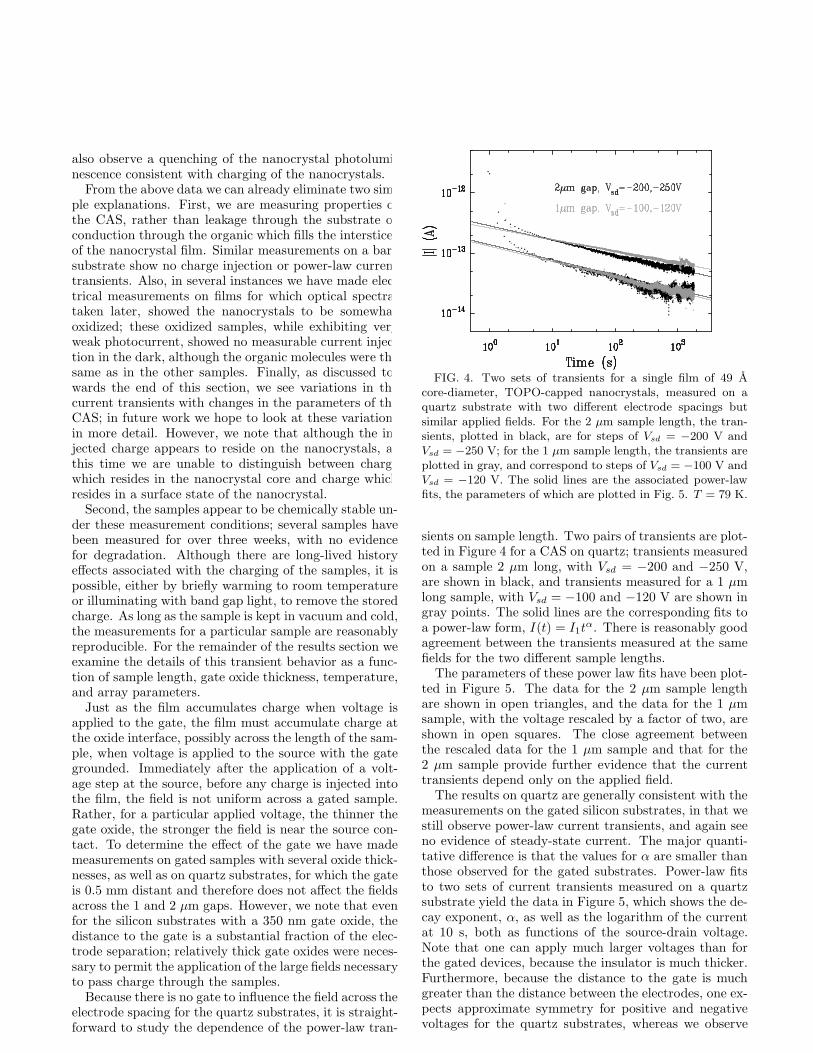
The results on quartz are generally consistent with themeasurements on the gated silicon substrates, in that westill observe power-law current transients, and again seeno evidence of steady-state current. The major quanti-tative difference is that the values for α are smaller thanthose observed for the gated substrates. Power-law fitsto two sets of current transients measured on a quartzsubstrate yield the data in Figure 5, which shows the de-cay exponent, α, as well as the logarithm of the currentat 10 s, both as functions of the source-drain voltage.Note that one can apply much larger voltages than forthe gated devices, because the insulator is much thicker.Furthermore, because the distance to the gate is muchgreater than the distance between the electrodes, one ex-pects approximate symmetry for positive and negativevoltages for the quartz substrates, whereas we observe
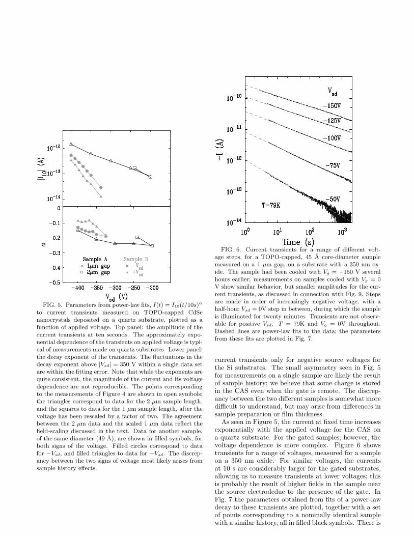
FIG. 5. Parameters from power-law fits, I(t) = I10(t/10s)α
to current transients measured on TOPO-capped CdSenanocrystals deposited on a quartz substrate, plotted as afunction of applied voltage. Top panel: the amplitude of thecurrent transients at ten seconds. The approximately expo-nential dependence of the transients on applied voltage is typi-cal of measurements made on quartz substrates. Lower panel:the decay exponent of the transients. The fluctuations in thedecay exponent above |Vsd| = 350 V within a single data setare within the fitting error. Note that while the exponents arequite consistent, the magnitude of the current and its voltagedependence are not reproducible. The points correspondingto the measurements of Figure 4 are shown in open symbols;the triangles correspond to data for the 2 µm sample length,and the squares to data for the 1 µm sample length, after thevoltage has been rescaled by a factor of two. The agreementbetween the 2 µm data and the scaled 1 µm data reflect thefield-scaling discussed in the text. Data for another sample,of the same diameter (49 A), are shown in filled symbols, forboth signs of the voltage. Filled circles correspond to datafor −Vsd, and filled triangles to data for +Vsd. The discrep-ancy between the two signs of voltage most likely arises fromsample history effects.
FIG. 6. Current transients for a range of different volt-age steps, for a TOPO-capped, 45 A core-diameter samplemeasured on a 1 µm gap, on a substrate with a 350 nm ox-ide. The sample had been cooled with Vg = −150 V severalhours earlier; measurements on samples cooled with Vg = 0V show similar behavior, but smaller amplitudes for the cur-rent transients, as discussed in connection with Fig. 9. Stepsare made in order of increasingly negative voltage, with ahalf-hour Vsd = 0V step in between, during which the sampleis illuminated for twenty minutes. Transients are not observ-able for positive Vsd. T = 79K and Vg = 0V throughout.Dashed lines are power-law fits to the data; the parametersfrom these fits are plotted in Fig. 7.
current transients only for negative source voltages forthe Si substrates. The small asymmetry seen in Fig. 5for measurements on a single sample are likely the resultof sample history; we believe that some charge is storedin the CAS even when the gate is remote. The discrep-ancy between the two different samples is somewhat moredifficult to understand, but may arise from differences insample preparation or film thickness.
As seen in Figure 5, the current at fixed time increasesexponentially with the applied voltage for the CAS ona quartz substrate. For the gated samples, however, thevoltage dependence is more complex. Figure 6 showstransients for a range of voltages, measured for a sampleon a 350 nm oxide. For similar voltages, the currentsat 10 s are considerably larger for the gated substrates,allowing us to measure transients at lower voltages; thisis probably the result of higher fields in the sample nearthe source electrodedue to the presence of the gate. InFig. 7 the parameters obtained from fits of a power-lawdecay to these transients are plotted, together with a setof points corresponding to a nominally identical samplewith a similar history, all in filled black symbols. There is

FIG. 7. Parameters from the power-law fits I = I1tα to
current transients measured for samples on gated substrates.Top panel: the amplitude of the transients at ten seconds.Lower panel: the decay exponent of the transients. Data for1 µm long samples on substrates with a 350 nm gate oxide areshown in black; the filled circles correspond to the dashed linesin Fig. 6, and the triangles come from measurements taken ona different but nominally identical sample. The filled squarescorrespond to measurements on the first sample, immediatelyafter cooling with Vg = 0V. Data for a sample of 45 A di-ameter nanocrystals measured on a substrate with a 500 nmoxide substrate are shown in gray, for two different samplelengths. The open triangles correspond to the 1 µm sample,and the open squares are data for the 2 µm long sample, afterdividing the voltage by a factor of 1.6. Transients are onlyobserved for negative Vsd on the gated substrates.
remarkably good agreement between the two sets of data.On the same axes are also plotted another set of points,which correspond to a set of transients measured for asample on a substrate with a 500 nm oxide. For bothtypes of gated substrate, the decay exponents becomesmaller with more negative Vsd, and the amplitude ofthe current at 10 s, as well as the exponent α, appear tosaturate as the size of the voltage step is increased.
Although the current transients scale with field on thequartz substrates, the scaling with applied voltage is dif-ferent for samples measured on gated substrates18. For a500 nm thick oxide, although we can find a voltage suchthat the transient on the 2 micron gap is the same asthat on the 1 micron gap, the voltages differ by a factorof 1.6 instead of 2. Interestingly, this single rescaling fac-tor persists over the entire voltage range for which thetransients are measurable. This is illustrated in Fig. 7,where the data for the 500 nm oxide substrates consist ofdata for a 1µm sample, shown in open triangles, as well asrescaled data for a 2 µm sample, shown in open squares.The scaling factor appears to be smaller still for the 350nm oxide. Thus it appears that the transients on quartzsubstrates depend only on the field, whereas for the sil-icon substrates, as the gate oxide thickness is reduced,the transients become less dependent on the electrodespacing, perhaps approaching a dependence only on thesource voltage.
The temperature dependence of the current transientsis shown in Figure 8, for measurements of a 1 µm longsample on a substrate with a 350 nm gate oxide; theseparameters are obtained from three-parameter power-lawfits to the transients, I(t) = I1t
α + Ileakage . In the toppanel, the current at ten seconds is plotted for three dif-ferent values of Vsd. Also shown is the steady-state leak-age current, which is identical to that measured on anequivalent device structure with no CAS film. This leak-age current is linear in voltage, and is well described byan activated form, I = I0 exp(−EA/kBT ), with an acti-vation energy EA = 370 meV. Clearly, the leakage cur-rent interferes with the measurements of the transients attemperatures above ∼ 220 K. The decay exponent of thecurrent transients is plotted in the lower panel. AlthoughFig. 8 shows only data from 77K to room temperature, aseparate set of measurements from 6K to 77K shows nosubstantial variation with temperature over that range.Above 77K, there is little variation in either of the param-eters until approximately 150K, above which the ampli-tude of the current transients increases and the power lawbecomes steeper. The decrease in the amplitude of thetransients above 220 K, and the associated sharp drop inthe decay exponent, is most likely an artifact associatedwith the leakage current.
In order to further explore the relationship betweenthe buildup of charge in the CAS and the current tran-sients, we have measured transients after cooling the sam-ples with an applied electric field. At room temperature,a voltage Vfc is applied to the gate, and the sample isthen cooled to 77 K. Once the sample is cold, the gate

FIG. 8. Temperature dependence of the current tran-sients measured on the same sample as in Fig. 6, takenin order of increasing temperature. The two parametersare obtained from three-parameter fits to the transients,I(t) = I10(t/10s)α + Ileakage , where Ileakage = 0 for T < 200K. Top panel: the amplitude of the current transients atten seconds. The dashed line indicates the value of Iss forVsd = −100 V, which is identical to that measured on a baresubstrate, and so is attributed to oxide leakage. Lower panel:the decay exponent of the transients, for the same values ofVsd. Note that the transients for Vsd = −100 V are too smallto fit below 150 K.
FIG. 9. Current transients for the same sample as in Fig.6, after cooling with different gate voltages, shown withpower-law fits (dashed lines). Before each transient, the sam-ple has been prepared by cooling from approximately 290Kto 78K with Vfc (labelled on the right) applied to the gate;after reaching 78K, Vg is set to 0V, and then Vsd is steppedto −125 V.
voltage is turned to zero, and only then is the sourcevoltage stepped. From the measurements of the tem-perature dependence of the transients, it appears thatcharge injected into the film equilibrates fairly rapidly atroom temperature. Furthermore, the measurements ofgate charging, shown in Fig. 3, demonstrate that oncecharge is injected into the CAS, it is difficult to removeat low temperatures. Therefore, in applying a gate volt-age at room temperature, the hope is to equilibrate thesample with a particular charge density at room temper-ature, and then to maintain that charge density after thegate voltage is turned to zero with the sample cold.
The results, for a set of transients measured with Vsd
steps to −125 V, are shown in Figure 9. When the sampleis cooled with a positive voltage on the gate, such thatexcess negative charge has been stored in the sample,the current transient is much smaller; conversely, coolingwith a negative voltage on the gate results in a muchlarger current. This is consistent with the decay of thecurrent in time; in both cases, the buildup of negativecharge increases the resistance. It also suggests that atroom temperature it may be possible to inject positivecharge, although, given the leakage current observed evenfor the bare substrates (Fig. 8), it remains possible thatsome of the charge injected at room temperature residesin the oxide rather than within the nanocrystal film.
The parameters of the current transients depend onthe size and spacing of the nanocrystals in the CAS. In

FIG. 10. Comparison of data from three chemically distincttypes of samples measured on substrates with 350 nm oxides,in a plot of the amplitude of the transients at ten secondsagainst the exponent of the decay, obtained from power-lawfits. In gray symbols are data from five different 45 A corediameter, TOPO-capped samples, after scaling for the filmthickness as described in the text. Data for the other twosamples are shown before rescaling as dashed lines, and afterrescaling, as filled black squares for the 40 A core-diameterTBPO-capped sample, and filled black triangles for a 66 A,TOPO-capped sample. The trends discussed previously, withapplied voltage and temperature, are indicated with arrows.
Figure 10 we look for trends with the sample parametersby plotting the amplitude of the current transient againstthe decay exponent α, for a number of different sampleswith 1 µm length measured on substrates with 350 nmoxides. Each line connects a series of measurements on asingle sample with different applied voltages (Vsd). Thegeneral direction of increasingly negative Vsd is indicatedby the arrows. Data for the most commonly used typeof sample, 45A core-diameter TOPO-capped nanocrys-tals, are shown for five different samples. Although thereis some spread among these points, data for the othertwo types of samples fall outside this spread. Data fora sample of 66A core-diameter, TOPO-capped nanocrys-tals show somewhat smaller values for |α| as well as theamplitude of the transients, corresponding to a slowerdecay of the current. Data for a sample of 40A core-diameter, TBPO-capped nanocrystals show larger valuesof |α|, as well as smaller amplitudes.
In making comparisons between different samples, it isnecessary to take the varying thicknesses of the films intoaccount; the data in Fig. 10 correspond to films whichrange in thickness from 100 to 900 nm, corresponding to20 to 180 layers of nanocrystals. As a first approxima-tion, we have assumed that the current is proportionalto the thickness of the film. The data for the standardsamples in Fig. 10 has already been scaled to correctfor the thickness; the clustering of these points indicatesthat the simple multiplicative correction is moderatelysuccessful, and suggests that the current distribution is
roughly uniform for these films. There is, nonetheless,one major difference for the thinner films, shown as tri-angles and asterisks; although the scaled points fall in thesame general area as those of the thicker samples, theyspan a much smaller range of α and I10 for the samerange in Vsd, suggesting a change in the voltage depen-dence of the transients. The dependence of the currenttransients on film thickness requires future attention, andcould be particularly interesting in the event that thetwo-dimensional limit could be more closely approached.
Discussion
The very high resistivity of our CAS films sug-gests that they contain no free carriers in the initialstate. Since such free carriers are thought to quenchphotoluminescence19, the high resistivity is therefore con-sistent with the relatively high quantum efficiencies foundin similar films. However, our experiments show that atsufficiently high voltages negative charge can be injectedinto the CAS from gold electrodes. Furthermore, oncethe charge is injected, it remains in the film for very longtimes at temperatures below 200K. The essential ques-tions raised by our experiments are why the charge isstored for such long times and what the relationship isbetween this stored charge and the observed power-lawdecay of the current.
We first focus on the quartz-substrate measurements,for which the gate affects neither the field nor the chargeaccumulation in the sample. The exponential voltage de-pendence of the current at fixed time might result fromfield emission of electrons from the Au into the CAS. Inthis case, one might argue that a buildup of charge nearthe source electrode would screen the field, reducing thethe field emission. Ginger et al. have developed sucha model to explain their observed current transients forCdSe nanocrystal arrays8. Using a sandwich-cell geome-try, with sample thicknesses of 100-200 nm, they find acurrent that decays as a stretched exponential in time. Inthis model, charge carriers move in a transport band untilthey become trapped in localized states. The buildup ofcharge reduces the field at the contact and consequentlythe injection current.
We find it difficult to reconcile this model with ourobservations. First, it is difficult to understand why ex-trinsic traps should lead to current transients whose ex-ponents change with the nanocrystal size and spacing.Second, in our measurements, orders of magnitude morecharge flows to the drain than is trapped in the sample.Since the trapping probability must therefore be small,the density of trapped charge should be approximatelyuniform across the sample. At later times, when thisuniform density of trapped charge becomes sufficient toprohibit injection from the contact, the current would notscale with the applied field. However, the current tran-sients we observe are field-dependent at all times; there is

no evidence for a significant buildup of charge within thesample during the measurement. Furthermore, becausethe amplitude of the transients grows exponentially withthe applied field, these measurements are fairly sensitiveto deviations from field-dependence.
Alternatively, the exponential voltage dependencecould arise from an exponential dependence of the hop-ping rate between nearest-neighbor nanocrystals. In thiscase, we propose that the current is not limited by in-jection into the sample, but rather by extraction from aspace charge region which forms near the contact. Thistype of space-charge limited current is common in in-sulators with low charge density; however, for the CASour observations differ from the conventional models ofspace charge limited current in two ways. First, in mostsystems, space-charge limited currents reach steady statewhen the integrated current is roughly equal to the totalamount of space charge which resides in the sample. Forthe CAS on quartz substrates, we estimate this time tobe t < 1 s, much shorter than the times over which weobserve the power law decay. From this, we are led topropose that although the space charge region developsfairly quickly, the extraction of carriers from the spacecharge region decreases with time.
Second, for conventional space charge limited current,although the space charge is concentrated near the in-jecting contact, there is typically a long tail in the distri-bution which extends across the sample. As a result, insystems where space charge limited current is observed,the current generally has some dependence on the sam-ple length as well as on the applied field20. However, inthe CAS films we observe field-dependence of the currenttransients, over a time range of 1000 s for measurementson the quartz substrates. This suggests that the spacecharge region which limits the transport in this systemis confined to a narrow region near the injecting contact.From the uncertainty associated with the scaling factor inour measurements, we estimate that this region extendsno further than 100 nm from the contact, or a tenth ofour smallest sample length. We note that our observa-tions are not entirely inconsistent with those of Ginger et
al., whose samples were considerably shorter than thosestudied here; a space charge region of 100 nm in theirsystem would extend halfway across the longest samples.
The power-law decay of the current is reminiscent ofthat associated with relaxation of carriers in GaAs21.The motion of electrons in a band of localized states withdisorder has been studied in great detail22. This systemhas a Coulomb gap for single-particle excitations, andthe ground state is highly degenerate. Together, thesegive rise to very slow relaxation times, and the systemhas been referred to as a Coulomb glass23. Such slowrelaxation has been suggested as the origin of unusualphenomena in indium oxide films24,25. We propose thatthe space charge near the source electrode is a Coulombglass. Although the space charge builds up in a very shorttime, the emission of electrons from the space charge re-gion decreases with time as the Coulomb glass relaxes
and the Coulomb gap grows in size. Presumably, oncesuch a Coulomb glass relaxes it will be removed fromthe sample only extremely slowly after the voltage is re-moved; this is consistent with the sample history effectswe observe as well as the charging measurements of Fig.3. The larger exponents observed as the temperature isincreased might result from more rapid relaxation of theCoulomb glass. A similar trend towards faster decay ofthe current is seen when changes in the array parameterslead to increased coupling between the dots, in Fig. 10.For the TBPO-capped sample, the nearest-neighbor sep-aration is 7A, compared to 11A for the standard, TOPO-capped dots10. Because inter-dot tunneling should in-crease exponentially as the width of the tunnel barrier isdecreased, we expect the change in capping molecules tolead to increased coupling between the dots. As for thetemperature dependence, the data suggest that increasedcoupling between the dots leads to a faster decay of thecurrent.
We have no quantitative theory with which to com-pare our results, and there are even qualitative observa-tions that we cannot explain. For example, it is clearthat the presence of a gate electrode will lead to addi-tional space charge in the sample, so it is not surpris-ing that the current transients are strongly modified asthe gate oxide is made thinner than the spacing betweensource and drain. The field which extracts charge fromthe space charge region near the injecting contact thenfalls between source and gate; it increases as the gate ox-ide thickness decreases, and becomes less dependent onthe electrode spacing. This is consistent with the data ofFig. 7, for which I(t, V, L) = I(t, 1.6V, 2L) for the 1 µmand 2 µm long samples on the gated substrates, ratherthan the strict field dependence observed for the quartzsubstrates. However, we do not understand why the ex-ponents of the current decay are larger for the gated sub-strates; in the Coulomb glass model the presence of morespace charge should lead to slower equilibration. We alsodo not know how to reconcile the smaller exponents ofthe power-law decay of the current when we apply thevoltage to the source compared with that which we ob-serve when voltage is applied to the gate.
Our future work will focus on making samples withstronger coupling between nanocrystals. Presumbablythis would make it possible to observe the hopping con-ductivity characteristic of the Coulomb gap.
ACKNOWLEDGMENTS
This work at MIT was supported by Award No. DMR9808941, under the MRSEC Program of the NSF. N.Y.M.acknowledges support from an ONR Graduate Fellowshipand from the Lucent Technologies Graduate ResearchProgram for Women.
1 C. Murray, C. Kagan, and M. Bawendi, Annual Review ofMaterial Science 30, 545 (2000).
2 C. Collier, T. Vossmeyer, and J. Heath, Annual Review ofPhysical Chemistry 49, 371 (1998).
3 D. L. Klein et al., Nature 389, 699 (1997).4 R. Ashoori, Nature 379, 413 (1996).5 M. Kastner, Physics Today 46, 24 (1993).6 B. Alperson, S. Cohen, I. Rubinstein, and G. Hodes, Phys-ical Review B 52, R17017 (1995).
7 D.S. Novikov, B. Kozinsky, and L.S. Levitov, cond-mat/0111345.
8 D. Ginger and N. Greenham, Journal of Applied Physics87, 1361 (2000).
9 C. Murray, D. Norris, and M. Bawendi, Journal of theAmerican Chemical Society 115, 8706 (1993).
10 C. Murray, C. Kagan, and M. Bawendi, Science 270, 1335(1995).
11 C. Leatherdale et al., Physical Review B 62, 2669 (2000).12 M. Drndic et al., To be published, 2002.13 Other measurements, made on substrates with circular
electrodes, are consistent with those shown here; for thesedevices, the active area of the film lies inside the outerelectrode, and so the similarity of the results confirms thispicture.
14 A stretched exponential decay will always be concave down-ward on a log-log plot, although with τ, β → 0 the formapproaches a straight line. Here we choose a characteris-tic time of τ = 1 ms, an order of magnitude shorter thanour earliest measurement time; longer values of τ wouldshow still more curvature. In the data from the sandwichstructures of Ref.8, typical values of τ were 10-500 seconds.
15 Although charge spreads into the film in all directions fromthe source electrode, the measured current arises only fromcharge which either passes into, or moves near to (relativeto the thickness of the gate oxide), the drain electrode.More distant charge will be screened by the gate electrode,which is grounded for the measurement. Therefore, whenestimating the possible contribution of stored charge to themeasured current, we consider only the area of the film be-tween the electrodes. Even if the entire surface of the sub-strate, except for the drain electrode, were charged to Vsd,this measurement would be sensitive only to charge aroundthe perimeter of the electrode, leading to a correction of lessthan a factor of ten.
16 In photoconductivity measurements on similar samples11,photocurrent several orders of magnitude larger than thedark current is observed. The spectral dependence of thephotocurrent is the same as the optical absorption of thenanocrystals. In the measurements discussed here, the cre-ation of electron-hole pairs in the nanocrystals apparentlymakes the CAS sufficiently conducting for the charge toreturn to ground.
17 W. Woo et al., To be published, 2002.18 Here, we use the word scaling in the general sense: to say
that the transients scale with the field is to say that I(t)depends only on E = Vsd/L, where L is the sample length,rather than I(t) ∝ E.
19 D. Chepic et al., Journal of Luminescence 47, 113 (1990).20 K. C. Hao and W. Hwang, Electrical transport in solids,
International series in the science of the solid state (Perg-
amon Press, 1981).21 D. Monroe et al., Physical Review Letters 59, 1148 (1987).22 A. Efros and B. Shklovskii, Journal of Physics C: Solid
State Physics 8, L49 (1975).23 J.H. Davies, P.A. Lee, and T.M. Rice, Physical Review B
29, 4260 (1984).24 M. Ben-Chorin, Z. Ovadyahu, and M. Pollak, Physical Re-
view B 48, 15025 (1993).25 A. Vaknin, Z. Ovadyahu, and M. Pollak, Physical Review
Letters 81, 669 (1998).


![Resonant Raman effect enhanced by surface plasmon excitation of CdSe nanocrystals embedded in thin SiO[sub 2] films](https://static.fdokumen.com/doc/165x107/634518516cfb3d40640985a1/resonant-raman-effect-enhanced-by-surface-plasmon-excitation-of-cdse-nanocrystals.jpg)


