
Colloidal CIGS and CZTS nanocrystals: A precursor route to printed photovoltaics
11
Colloidal CIGS and CZTS nanocrystals: A precursor route to printed photovoltaics Vahid A. Akhavan, Brian W. Goodfellow, Matthew G. Panthani, Chet Steinhagen, Taylor B. Harvey, C. Jackson Stolle, Brian A. Korgel n Department of Chemical Engineering, Texas Materials Institute and Center for Nano- and Molecular Science and Technology, The University of Texas at Austin, Austin, TX 78712-1062, USA article info Available online 10 November 2011 Keywords: Nanocrystals Photovoltaics Energy Sustainability Printed electronics abstract This review article summarizes our research focused on Cu(In 1–x Ga x )Se 2 (CIGS) nanocrystals, including their synthesis and implementation as the active light absorbing material in photovoltaic devices (PVs). CIGS PV layers are typically made using a high temperature ( 4450 1C) process in which Cu, In and Ga are sequentially or co-evaporated and selenized. We have sought to use CIGS nanocrystals synthesized with the desired stoichiometry to deposit PV device layers without high temperature processing. This approach, using spray deposition of the CIGS light absorber layers, without high temperature selenization, has enabled up to 3.1% power conversion efficiency under AM 1.5 solar illumination. Although the device efficiency is too low for commercialization, these devices provide a proof-of- concept that solution-deposited CIGS nanocrystal films can function in PV devices, enabling unconven- tional device architectures and materials combinations, including the use of flexible, inexpensive and light-weight plastic substrates. & 2011 Elsevier Inc. All rights reserved. 1. Introduction With global energy consumption continuing to rise, renewable energy resources have become increasingly important. The sun provides an abundant source of sustainable energy—enough to supply all of humanity’s primary energy needs [1]. Sunlight can be conveniently converted directly to electricity by photovoltaic (PV) devices, and therefore, PVs have been integrated into the electricity grid and installed as point-of-use sources for off-grid power. Nonetheless, PV power is expensive and costs significantly more than fossil fuels. In early 2011, the average retail price of PV-generated elec- tricity was 0.207 $/kWh [2], compared to an average of 0.097 $/ kWh for conventional sources of electricity [3]. PV power, more readily measured as a price per Watt generated at peak perfor- mance during the day, or peak Watt (W p ), needs to reach about $1/W p for grid parity [4,5]. This price reflects the ratio of cost associated with module production and installation to the device efficiency under realistic peak operating conditions. Significant progress towards the goal of $1/W p has been made during the past decade, primarily with advances in thin film PV technologies like CdTe-based cells, but there is still a significant economic gap [4]. Thin film PVs have lower power conversion efficiency (PCE), of about 13% compared to 15–18%, than the crystalline silicon-based solar cells that currently dominate the market [6], but they can be manufactured at much lower cost, thus signifi- cantly reducing the total cost of the electricity [7]. The price of thin film PV electricity could be further reduced by significantly increasing device efficiency while retaining low manufacturing costs. PVs with significantly higher efficiency and high power density can be made, like the single junction single-crystal modules approaching the Shockley–Queisser limit ( 31%) [8] and very high efficiency multijunction cells [9] developed for space applications, but these technologies are far too expensive for general terrestrial use. Therefore, there is an effort to create a new generation of high efficiency PVs that can be manufactured at low cost. We have sought to develop such a materials system, with the long-term goal of creating light-absorbing materials that can be processed into high-efficiency multijunction thin film PVs at low cost. Multijunction thin film PV devices will require new combi- nations of semiconductor materials and electrode layers. Each processing step must not harm the underlying device layers and therefore, deposition strategies that require only mild conditions are particularly important. Our approach has been to develop nanocrystal inks to yield inorganic thin films under ambient or mild processing conditions, ideally in a high-throughput printing process, like a roll-to-roll scheme [10]. The ability to deposit Contents lists available at SciVerse ScienceDirect journal homepage: www.elsevier.com/locate/jssc Journal of Solid State Chemistry 0022-4596/$ - see front matter & 2011 Elsevier Inc. All rights reserved. doi:10.1016/j.jssc.2011.11.002 n Corresponding author. Fax: þ1 512 471 7060. E-mail address: [email protected] (B.A. Korgel). Journal of Solid State Chemistry 189 (2012) 2–12
Transcript of Colloidal CIGS and CZTS nanocrystals: A precursor route to printed photovoltaics

Journal of Solid State Chemistry 189 (2012) 2–12
Contents lists available at SciVerse ScienceDirect
Journal of Solid State Chemistry
0022-45
doi:10.1
n Corr
E-m
journal homepage: www.elsevier.com/locate/jssc
Colloidal CIGS and CZTS nanocrystals: A precursor route toprinted photovoltaics
Vahid A. Akhavan, Brian W. Goodfellow, Matthew G. Panthani, Chet Steinhagen, Taylor B. Harvey,C. Jackson Stolle, Brian A. Korgel n
Department of Chemical Engineering, Texas Materials Institute and Center for Nano- and Molecular Science and Technology, The University of Texas at Austin,
Austin, TX 78712-1062, USA
a r t i c l e i n f o
Available online 10 November 2011
Keywords:
Nanocrystals
Photovoltaics
Energy
Sustainability
Printed electronics
96/$ - see front matter & 2011 Elsevier Inc. A
016/j.jssc.2011.11.002
esponding author. Fax: þ1 512 471 7060.
ail address: [email protected] (B.A. Korg
a b s t r a c t
This review article summarizes our research focused on Cu(In1–xGax)Se2 (CIGS) nanocrystals, including
their synthesis and implementation as the active light absorbing material in photovoltaic devices (PVs).
CIGS PV layers are typically made using a high temperature (4450 1C) process in which Cu, In and Ga
are sequentially or co-evaporated and selenized. We have sought to use CIGS nanocrystals synthesized
with the desired stoichiometry to deposit PV device layers without high temperature processing.
This approach, using spray deposition of the CIGS light absorber layers, without high temperature
selenization, has enabled up to 3.1% power conversion efficiency under AM 1.5 solar illumination.
Although the device efficiency is too low for commercialization, these devices provide a proof-of-
concept that solution-deposited CIGS nanocrystal films can function in PV devices, enabling unconven-
tional device architectures and materials combinations, including the use of flexible, inexpensive and
light-weight plastic substrates.
& 2011 Elsevier Inc. All rights reserved.
1. Introduction
With global energy consumption continuing to rise, renewableenergy resources have become increasingly important. The sunprovides an abundant source of sustainable energy—enough tosupply all of humanity’s primary energy needs [1]. Sunlight canbe conveniently converted directly to electricity by photovoltaic(PV) devices, and therefore, PVs have been integrated into theelectricity grid and installed as point-of-use sources for off-gridpower. Nonetheless, PV power is expensive and costs significantlymore than fossil fuels.
In early 2011, the average retail price of PV-generated elec-tricity was 0.207 $/kWh [2], compared to an average of 0.097 $/kWh for conventional sources of electricity [3]. PV power, morereadily measured as a price per Watt generated at peak perfor-mance during the day, or peak Watt (Wp), needs to reach about$1/Wp for grid parity [4,5]. This price reflects the ratio of costassociated with module production and installation to the deviceefficiency under realistic peak operating conditions. Significantprogress towards the goal of $1/Wp has been made during thepast decade, primarily with advances in thin film PV technologieslike CdTe-based cells, but there is still a significant economic
ll rights reserved.
el).
gap [4]. Thin film PVs have lower power conversion efficiency(PCE), of about 13% compared to 15–18%, than the crystallinesilicon-based solar cells that currently dominate the market [6],but they can be manufactured at much lower cost, thus signifi-cantly reducing the total cost of the electricity [7]. The price ofthin film PV electricity could be further reduced by significantlyincreasing device efficiency while retaining low manufacturingcosts. PVs with significantly higher efficiency and high powerdensity can be made, like the single junction single-crystalmodules approaching the Shockley–Queisser limit (�31%) [8]and very high efficiency multijunction cells [9] developed forspace applications, but these technologies are far too expensivefor general terrestrial use. Therefore, there is an effort to create anew generation of high efficiency PVs that can be manufacturedat low cost.
We have sought to develop such a materials system, with thelong-term goal of creating light-absorbing materials that can beprocessed into high-efficiency multijunction thin film PVs at lowcost. Multijunction thin film PV devices will require new combi-nations of semiconductor materials and electrode layers. Eachprocessing step must not harm the underlying device layers andtherefore, deposition strategies that require only mild conditionsare particularly important. Our approach has been to developnanocrystal inks to yield inorganic thin films under ambient ormild processing conditions, ideally in a high-throughput printingprocess, like a roll-to-roll scheme [10]. The ability to deposit
V.A. Akhavan et al. / Journal of Solid State Chemistry 189 (2012) 2–12 3
semiconductor layers in this way would enable low manufactur-ing costs while providing inorganic layers that have the potentialfor devices with high power conversion efficiency and goodphotostability. Such a materials system would also enable fabri-cation of thin film inorganic PVs on light-weight and flexibleplastic substrates.
2. CIGS nanocrystal inks for printed PVs
Our research has primarily focused on Cu(In1–xGax)Se2 (CIGS)nanocrystals. Of the thin film semiconductors (i.e., CdTe andamorphous Si), CIGS has yielded the highest efficiency of morethan 20% PCE [12]. CIGS has a direct band gap that is tunable inenergy from 1.0 to 1.6 eV, depending on the Ga concentration[11], it tolerates relatively large concentrations of grain bound-aries and has good photostability [13]. A variety of other thin filmabsorber materials exist, including InP, PbSe, FeS2 and Cu2ZnSnS4
(CZTS), but these have not been commercialized because theirdemonstrated laboratory efficiencies have been too low. But CIGSPVs have not been as commercially successful as CdTe andamorphous Si (a-Si). For high efficiency devices, CIGS films arevapor-deposited and processed at high temperature (4500 1C)under selenium atmosphere to obtain the desired crystal phaseand composition. This process has thus far been too expensive.
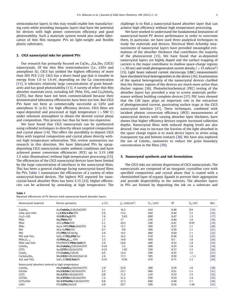
We have found that CIGS nanocrystals can be synthesizedusing colloidal techniques to directly obtain targeted compositionand crystal phase [14]. This offers the possibility to deposit CIGSfilms with targeted composition and crystal phase directly with-out high temperature selenization. This review summarizes ourresearch in this direction. We have fabricated PVs by spray-depositing CIGS nanocrystals under ambient conditions and haveachieved power conversion efficiencies (PCE) up to 3.1% (AM1.5 solar illumination) without high temperature processing [15].The efficiencies of the CIGS nanocrystal devices have been limitedby the large concentration of interfaces in the nanocrystal films.This has been a general challenge facing nanocrystal-based filmsfor PVs. Table 1 summarizes the efficiencies of a variety of othernanocrystal-based devices. The highest PCE reported for nano-crystal-based absorber films has been 5.1% [23]. Higher efficien-cies can be achieved by annealing at high temperature. The
Table 1Reported efficiencies of PV devices with nanocrystal-based absorber layers.
Nanocrystal material Device geometry Z (%)
CuInSe2 Au/CuInSe2/CdS/ZnO/ITO 3.1
CdSe and CdTe Ca/CdTe/CdSe/ITO 2.9
Cu2S–CdS Al/CdS/Cu2S/ITO 1.6
PbSe Mg/PbSe/ITO 1.1
PbSe Al/Ca/PbSe/ITO 2.1
PbSe Au/a-NPD/PbSe/ZnO/ITO 1.6
PbS Al/a-Si/PbS/ITO 0.7
PbS ITO/PbS/LiF/Al/Ag 3.9
PbS and TiO2 SnO2:F/TiO2/PbS/Au 5.1
PbSeXS1–X Al/PbSeXS1–x /ITO 3.3
PbSe and ZnO ITO/PEDOT/PbSe/ZnO/Al 3.4
CuInSe2 Mo/CuInSe2/CdS/ZnO/ITO 0.24
CZTS Au/CZTS/CdS/ZnO/ITO 0.23
CuInS2 ITO/CuInS2/CdS/Al 4.0
Cu(InGa)Se2 Mo/CIGS/CdS/ZnO/ZnO:Al 2.6
SnS and TiO2 SnO2:F/TiO2/SnS/Pt 0.10
Nanocrystal absorbers sintered at high temperatures
CuInSe2 Mo/CuInSe2/CdS/ZnO/ITO 2.8
CIGSSe Mo/CIGSSe/CdS/ZnO/ITO 5.5
CZTS Mo/CZTS/CdS/ZnO/ITO 0.8
CZTSSe Mo/CZTSSe/CdS/ZnO/ITO 7.2
CZTGeSSe Mo/CZTGeSSe/CdS/ZnO/ITO 6.8
CdTe ITO/CdTe/ZnO/Al 6.9
challenge is to find a nanocrystal-based absorber layer that canachieve high efficiency without high temperature processing.
We have worked to understand the fundamental limitations ofnanocrystal-based PV device performance in order to overcomethem. In particular, we have used three analytical techniques tostudy the materials and devices. Electrical Mott–Schottky mea-surements of nanocrystal layers have provided meaningful esti-mations of the absorber thickness that contributes the majorityof the photocurrent [15]. We have found that as-depositednanocrystal layers are highly doped and the surface trapping ofcarriers is the major contributor to shallow space-charge regions(E50 nm) and small photogenerated current density (o15 mA/cm2)[15]. Light beam induced current microscopy (LBIC) measurementshave elucidated local heterogeneities in the device [36]. Examinationof the spatial heterogeneity of the nanocrystal devices clarifiedthat the thinner regions of the devices are much more active thanthicker regions [36]. Photoelectrochemical (PEC) testing of theabsorber layers has provided a way to screen materials perfor-mance without building complete devices [37]. PEC tests showedthat the CdS layer plays an important role in the extractionof photogenerated current, passivating surface traps at the CIGSnanocrystal interface [37]. These techniques, combined withincident photon conversion efficiency (IPCE) measurements ofnanocrystal devices with varying absorber layer thickness, haveshown that higher efficiency devices require increased collectiondepths. Nanocrystal films with reduced doping levels are alsodesired. One way to increase the fraction of the light absorbed inthe space charge region is to stack device layers in series usingtransparent top and bottom contacts [38]. We have also exploredthe use of CuInSe2 nanowires to reduce the grain boundaryconcentration in the films [39].
3. Nanocrystal synthesis and ink formulation
The CIGS inks are solvent dispersions of CIGS nanocrystals. Thenanocrystals are composed of an inorganic crystalline core withspecified composition and crystal phase that is coated with achemisorbed layer of organic ligands to prevent their aggregationand provide dispersibility in the solvents. The absorber layersin PVs are formed by depositing the ink on a substrate and
Jsc (mA/cm2) Voc (mV) FF Eg (eV) Ref.
16.3 410 0.46 0.9 [15]
13.2 450 0.49 1.5 [16]
5.63 600 0.47 1.3 [17]
17 230 0.40 1.0 [18]
24.5 240 0.41 0.95 [19]
15.7 390 0.27 1.1 [20]
9.0 200 0.39 1.1 [21]
14.5 460 0.64 1.1 [22]
16.2 510 0.58 1.3 [23]
14.8 450 0.5 1.0 [24]
24.0 440 0.32 1.4 [25]
3.2 300 0.25 1.0 [14]
1.95 320 0.37 1.5 [26]
12.4 590 0.55 1.5 [27]
17.3 305 0.50 o1.1 [28]
0.30 470 0.71 1.3 [29]
25.8 280 0.39 1.0 [30]
23.7 460 0.51 1.1 [31]
11.5 210 0.33 1.5 [32]
31.2 430 0.54 1.4 [33]
21.5 640 0.49 1.1 [34]
20.7 590 0.56 1.44 [35]

V.A. Akhavan et al. / Journal of Solid State Chemistry 189 (2012) 2–124
evaporating the solvent to leave a dry nanocrystal film. Anysolution deposition technique can work, including spray deposi-tion, roll coating, doctor blading, spin coating, drop casting, dipcoating, ink-jet printing or screen printing, to name a few, as longas the deposited nanocrystal film is relatively uniform and free ofcracks [40].
The nanocrystals are synthesized by arrested precipitationfrom molecular precursors in a hot coordinating solvent to controlparticle growth. Colloidal chemical routes now exist for making awide variety of semiconductor nanocrystals, including GroupsII–VI [41], III–V [42], I–VI [43–45], IV–VI [46] and IV [47–50]materials. A wide variety of ternary and quaternary compoundscan also be made, including CuInS2 [14,51,52], CuInSe2 [14,30,53,54], CuGaSe2 [14,54], CIGS [14,54] and CZTS [26,33,55]. Below,we discuss the synthesis of CuInS2, CIGS and CZTS nanocrystals.
3.1. CuInS2 nanocrystals
When we began our search for a synthetic route to CIGSnanocrystals about six years ago, we started with the simpler,but related compound, CuInS2 [14]. The synthesis of CuInS2
nanocrystals was an important milestone for us, as it establishedthat a ternary compound semiconductor with chalcopyrite crystalstructure could be made with high phase purity and high yield
Fig. 1. TEM images of (A–B) CuInS2, (E–F) CIGS and (I–J) CZTS nanocrystals. (C) XRD pa
and (H) absorbance spectrum of CIGS nanocrystals with varying In:Ga ratios. (K) XRD
permission from Panthani et al. [14] and Steinhagen et al. [26]. Copyright 2008 and 20
without complicated chemistry like the use of single-sourcereactants or exotic reaction schemes [56]. Ultimately, the synth-esis that worked best for us was the method we had developed forcopper sulfide nanocrystals [57] with the addition to the reactionof In(acac)3 as an In source [14]:
CuðacacÞ2þ InðacacÞ3þ2S �������������!o-dichlorobenzene, 180 oC
oleylamine
CuInS2 nanocrystalsþbyproducts ð1Þ
This approach yields chalcopyrite CuInS2 nanocrystals in highyield and relatively narrow polydispersity, as shown in Fig. 1.
3.2. CuInSe2 nanocrystals
CuInSe2 nanocrystals could be synthesized using chemistrysimilar to the CuInS2 synthesis, with a modification of the solventsystem because unlike elemental sulfur, Se does not dissolve indichlorobenzene. Oleylamine was found to be a good solvent forSe, it has a sufficiently high boiling point for the synthesis, andwas observed to serve as an effective capping ligand for theCuInSe2 nanocrystals. We have explored a number of variations inreactant chemistry, but one effective route involves the simpleaddition of Cu and In salts with solid Se to oleylamine, followed
ttern and (D) absorbance spectrum of CuInS2 nanocrystal product. (G) XRD pattern
patter and (L) absorbance spectrum of CZTS nanocrystal product. Reprinted with
09 American Chemical Society.
V.A. Akhavan et al. / Journal of Solid State Chemistry 189 (2012) 2–12 5
by heating to 240 1C for 4 h:
CuClþ InCl3þ2Se�������������!oleylamine
240 oCCuInSe2 nanocrystalsþbyproducts
ð2Þ
Fig. 1 shows TEM images of CuInSe2 nanocrystals. Using thisapproach, the nanocrystals are irregularly shaped and ratherpolydisperse. One useful modification of the CuInSe2 nanocrystalsynthesis has been a hot injection method in which Cu and Inchloride are dissolved in oleylamine and then a complex oftributylphosphine and Se (TBP:Se) is injected at 180 1C. Thisreaction gives a slightly lower yield compared to the reactionwith elemental Se (Eq. (2)), but the PV device efficiencies have beenbetter using these nanocrystals. The TBP:Se reaction seems to becleaner, as the supernatant during the initial solvent washing stepsis almost clear and colorless, compared to a typically cloudy anddark supernatant in the elemental Se reaction. In another modifica-tion of the hot injection method using selenourea as a Se source,very monodisperse trigonal pyramidal CuInSe2 nanocrystals couldbe synthesized [53].
3.3. Cu(InxGa1–x)Se2 (CIGS) nanocrystals
It was found that Ga could be readily incorporated into theCuInSe2 nanocrystals during the synthesis to obtain CIGS withcontrolled In:Ga compositions. For example, GaCl3 could be addedto the reaction shown in Eq. (2):
CuClþð1�xÞInCl3þxGaCl3þ2Se�������������!oleylamine
240 oC
CuðIn1�xGaxÞSe2 nanocrystalsþbyproducts ð3Þ
The In:Ga ratio in the nanocrystals could be tuned system-atically by simply changing the proportion of Ga and In reactant.The CIGS nanocrystals have similar morphology as the CuInSe2
nanocrystals and Ga incorporation is evident from the XRDpatterns. The lattice constant determined by XRD, as shown forexample in Fig. 1, shift to slightly higher values of 2y as more Gais incorporated into the nanocrystals. EDS mapping of the nano-crystal composition also confirmed that the nanocrystals werecomposed of CIGS, and the optical gap measured by UV–visabsorbance spectroscopy increased in energy as expected withlarger Ga:In ratios [14].
3.4. Cu2ZnSnS4 (CZTS) nanocrystals
There is concern that the price of In and Ga in CIGS maypotentially become a problem and PV absorber materials com-posed of earth-abundant elements have been sought [58].Cu2ZnSnS4 (CZTS) has a very similar crystal structure to CIGSwith optical properties that are well-suited for PV applicationsand it has become a material of significant interest as a promisingnew photovoltaic material. CZTS has not been studied as exten-sively as CIGS and the best CZTS solar cells have achieved PCEs of9.7% utilizing a solution-processing method [59].
We were able to make CZTS nanocrystals using a chemicalapproach very similar to the CIGS synthesis [26]. For example, amixture of copper acetylacetonate, zinc acetate, tin chloridedihydrate and elemental sulfur in oleylamine heated to 280 1Cfor 1 h under an inert atmosphere provides a high yield of phasepure CZTS nanocrystals. TEM images of the product are shown inFig. 1I and J. The nanocrystals are slightly irregular in shape withan average diameter of about 10 nm. They are crystalline withXRD patterns that index to the kesterite phase of CZTS (Fig. 1K).The band gap energy determined from the optical absorbancespectrum of a nanocrystal dispersion is �1.3 eV, which is close tothat of bulk CZTS (1.5 eV).
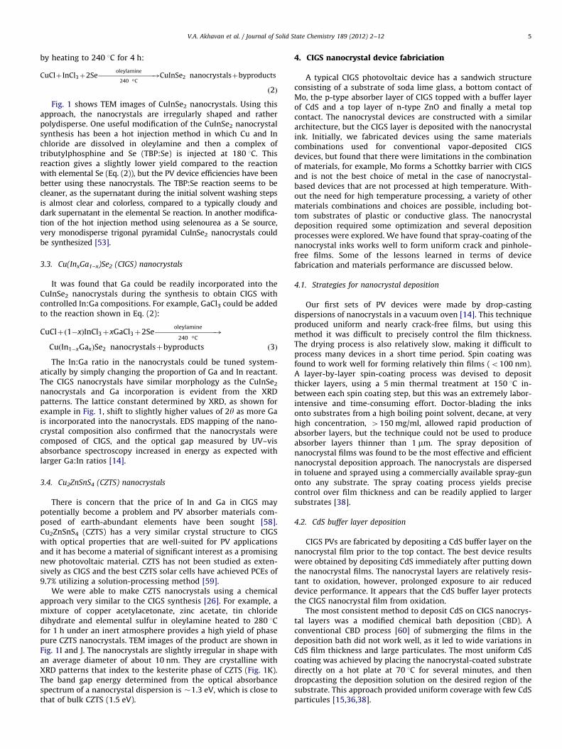
4. CIGS nanocrystal device fabriciation
A typical CIGS photovoltaic device has a sandwich structureconsisting of a substrate of soda lime glass, a bottom contact ofMo, the p-type absorber layer of CIGS topped with a buffer layerof CdS and a top layer of n-type ZnO and finally a metal topcontact. The nanocrystal devices are constructed with a similararchitecture, but the CIGS layer is deposited with the nanocrystalink. Initially, we fabricated devices using the same materialscombinations used for conventional vapor-deposited CIGSdevices, but found that there were limitations in the combinationof materials, for example, Mo forms a Schottky barrier with CIGSand is not the best choice of metal in the case of nanocrystal-based devices that are not processed at high temperature. With-out the need for high temperature processing, a variety of othermaterials combinations and choices are possible, including bot-tom substrates of plastic or conductive glass. The nanocrystaldeposition required some optimization and several depositionprocesses were explored. We have found that spray-coating of thenanocrystal inks works well to form uniform crack and pinhole-free films. Some of the lessons learned in terms of devicefabrication and materials performance are discussed below.
4.1. Strategies for nanocrystal deposition
Our first sets of PV devices were made by drop-castingdispersions of nanocrystals in a vacuum oven [14]. This techniqueproduced uniform and nearly crack-free films, but using thismethod it was difficult to precisely control the film thickness.The drying process is also relatively slow, making it difficult toprocess many devices in a short time period. Spin coating wasfound to work well for forming relatively thin films (o100 nm).A layer-by-layer spin-coating process was devised to depositthicker layers, using a 5 min thermal treatment at 150 1C in-between each spin coating step, but this was an extremely labor-intensive and time-consuming effort. Doctor-blading the inksonto substrates from a high boiling point solvent, decane, at veryhigh concentration, 4150 mg/ml, allowed rapid production ofabsorber layers, but the technique could not be used to produceabsorber layers thinner than 1 mm. The spray deposition ofnanocrystal films was found to be the most effective and efficientnanocrystal deposition approach. The nanocrystals are dispersedin toluene and sprayed using a commercially available spray-gunonto any substrate. The spray coating process yields precisecontrol over film thickness and can be readily applied to largersubstrates [38].
4.2. CdS buffer layer deposition
CIGS PVs are fabricated by depositing a CdS buffer layer on thenanocrystal film prior to the top contact. The best device resultswere obtained by depositing CdS immediately after putting downthe nanocrystal films. The nanocrystal layers are relatively resis-tant to oxidation, however, prolonged exposure to air reduceddevice performance. It appears that the CdS buffer layer protectsthe CIGS nanocrystal film from oxidation.
The most consistent method to deposit CdS on CIGS nanocrys-tal layers was a modified chemical bath deposition (CBD). Aconventional CBD process [60] of submerging the films in thedeposition bath did not work well, as it led to wide variations inCdS film thickness and large particulates. The most uniform CdScoating was achieved by placing the nanocrystal-coated substratedirectly on a hot plate at 70 1C for several minutes, and thendropcasting the deposition solution on the desired region of thesubstrate. This approach provided uniform coverage with few CdSparticules [15,36,38].
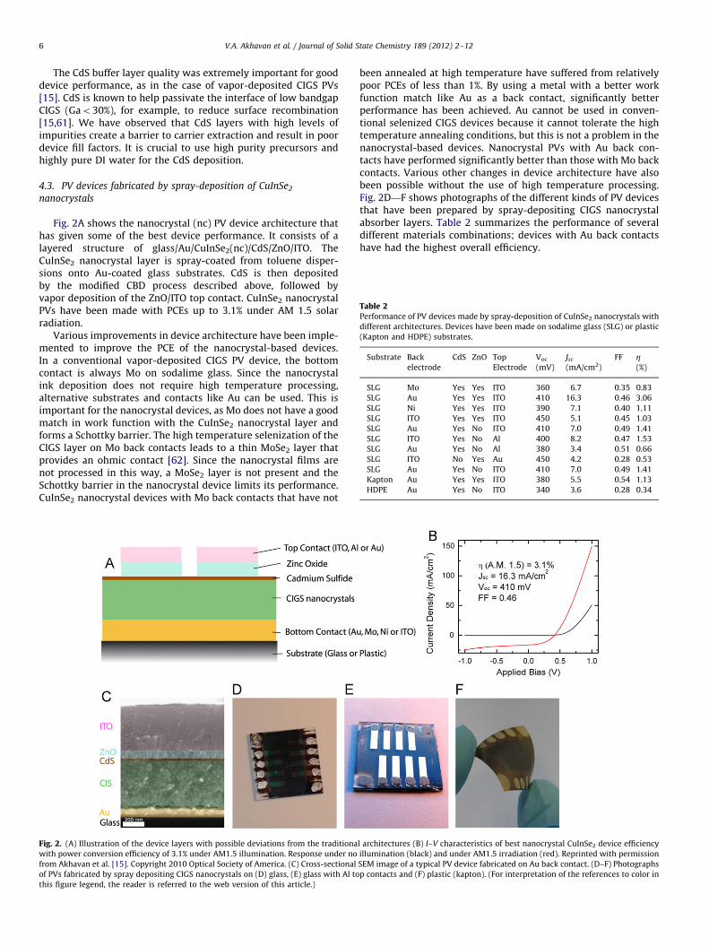
Table 2Performance of PV devices made by spray-deposition of CuInSe2 nanocrystals with
different architectures. Devices have been made on sodalime glass (SLG) or plastic
(Kapton and HDPE) substrates.
Substrate Back
electrode
CdS ZnO Top
Electrode
Voc
(mV)
Jsc
(mA/cm2)
FF Z(%)
SLG Mo Yes Yes ITO 360 6.7 0.35 0.83
SLG Au Yes Yes ITO 410 16.3 0.46 3.06
SLG Ni Yes Yes ITO 390 7.1 0.40 1.11
SLG ITO Yes Yes ITO 450 5.1 0.45 1.03
SLG Au Yes No ITO 410 7.0 0.49 1.41
SLG ITO Yes No Al 400 8.2 0.47 1.53
SLG Au Yes No Al 380 3.4 0.51 0.66
SLG ITO No Yes Au 450 4.2 0.28 0.53
SLG Au Yes No ITO 410 7.0 0.49 1.41
Kapton Au Yes Yes ITO 380 5.5 0.54 1.13
HDPE Au Yes No ITO 340 3.6 0.28 0.34
V.A. Akhavan et al. / Journal of Solid State Chemistry 189 (2012) 2–126
The CdS buffer layer quality was extremely important for gooddevice performance, as in the case of vapor-deposited CIGS PVs[15]. CdS is known to help passivate the interface of low bandgapCIGS (Gao30%), for example, to reduce surface recombination[15,61]. We have observed that CdS layers with high levels ofimpurities create a barrier to carrier extraction and result in poordevice fill factors. It is crucial to use high purity precursors andhighly pure DI water for the CdS deposition.
4.3. PV devices fabricated by spray-deposition of CuInSe2
nanocrystals
Fig. 2A shows the nanocrystal (nc) PV device architecture thathas given some of the best device performance. It consists of alayered structure of glass/Au/CuInSe2(nc)/CdS/ZnO/ITO. TheCuInSe2 nanocrystal layer is spray-coated from toluene disper-sions onto Au-coated glass substrates. CdS is then depositedby the modified CBD process described above, followed byvapor deposition of the ZnO/ITO top contact. CuInSe2 nanocrystalPVs have been made with PCEs up to 3.1% under AM 1.5 solarradiation.
Various improvements in device architecture have been imple-mented to improve the PCE of the nanocrystal-based devices.In a conventional vapor-deposited CIGS PV device, the bottomcontact is always Mo on sodalime glass. Since the nanocrystalink deposition does not require high temperature processing,alternative substrates and contacts like Au can be used. This isimportant for the nanocrystal devices, as Mo does not have a goodmatch in work function with the CuInSe2 nanocrystal layer andforms a Schottky barrier. The high temperature selenization of theCIGS layer on Mo back contacts leads to a thin MoSe2 layer thatprovides an ohmic contact [62]. Since the nanocrystal films arenot processed in this way, a MoSe2 layer is not present and theSchottky barrier in the nanocrystal device limits its performance.CuInSe2 nanocrystal devices with Mo back contacts that have not
Fig. 2. (A) Illustration of the device layers with possible deviations from the traditiona
with power conversion efficiency of 3.1% under AM1.5 illumination. Response under no
from Akhavan et al. [15]. Copyright 2010 Optical Society of America. (C) Cross-sectional
of PVs fabricated by spray depositing CIGS nanocrystals on (D) glass, (E) glass with Al to
this figure legend, the reader is referred to the web version of this article.)
been annealed at high temperature have suffered from relativelypoor PCEs of less than 1%. By using a metal with a better workfunction match like Au as a back contact, significantly betterperformance has been achieved. Au cannot be used in conven-tional selenized CIGS devices because it cannot tolerate the hightemperature annealing conditions, but this is not a problem in thenanocrystal-based devices. Nanocrystal PVs with Au back con-tacts have performed significantly better than those with Mo backcontacts. Various other changes in device architecture have alsobeen possible without the use of high temperature processing.Fig. 2D—F shows photographs of the different kinds of PV devicesthat have been prepared by spray-depositing CIGS nanocrystalabsorber layers. Table 2 summarizes the performance of severaldifferent materials combinations; devices with Au back contactshave had the highest overall efficiency.
l architectures (B) I–V characteristics of best nanocrystal CuInSe2 device efficiency
illumination (black) and under AM1.5 irradiation (red). Reprinted with permission
SEM image of a typical PV device fabricated on Au back contact. (D–F) Photographs
p contacts and (F) plastic (kapton). (For interpretation of the references to color in
V.A. Akhavan et al. / Journal of Solid State Chemistry 189 (2012) 2–12 7
4.4. Thickness-limited nanocrystal device performance
To date, devices made with CIGS nanocrystal absorber layersthat have not been selenized at high temperature have hadrelatively low short circuit current density (Jsc), leading to modestpower conversion efficiency. Vapor-deposited CIGS absorberlayers processed under typical high temperature selenizationconditions can have Jsc values above 40 mA/cm2 [62], while ourbest nanocrystal-based devices have had Jsc values of 16 mA/cm2.The highest efficiency nanocrystal-based devices have also been
Fig. 3. (A) IPCE measurements of PV devices made with varying CuInSe2 nanocrystal lay
the data in (A) to IQE based on the amount of light absorbed by the nanocrystal layer a
2010 Optical Society of America.
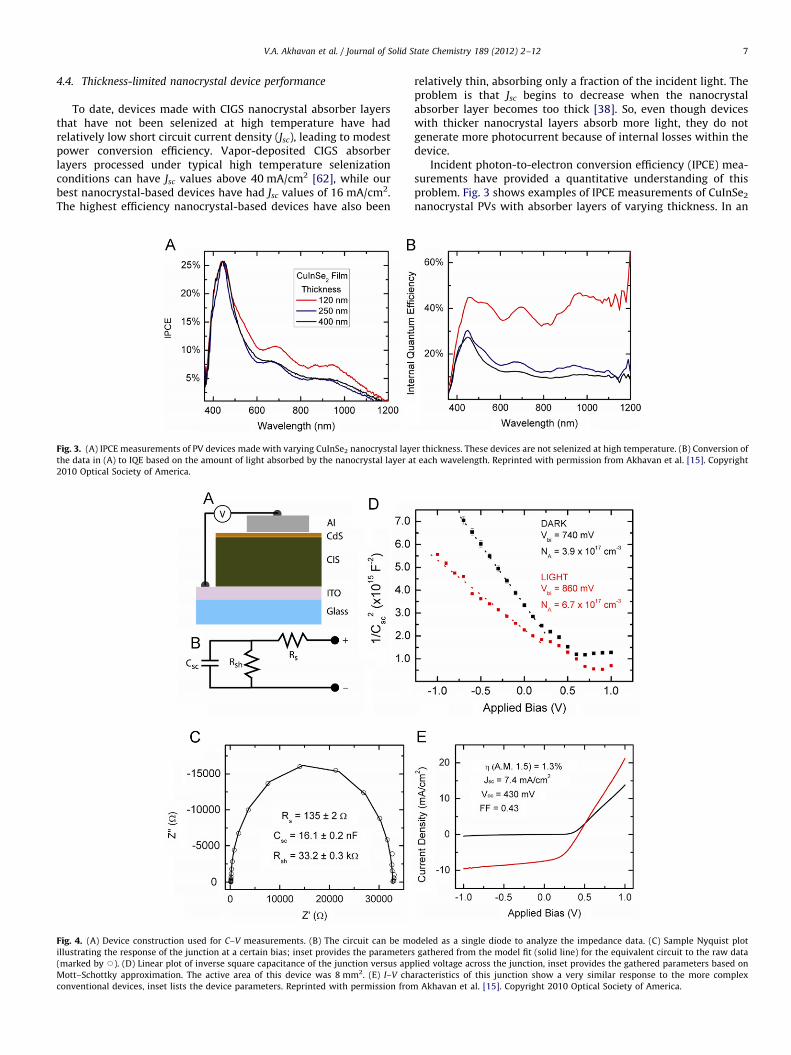
Fig. 4. (A) Device construction used for C–V measurements. (B) The circuit can be mo
illustrating the response of the junction at a certain bias; inset provides the parameter
(marked by J). (D) Linear plot of inverse square capacitance of the junction versus app
Mott–Schottky approximation. The active area of this device was 8 mm2. (E) I–V cha
conventional devices, inset lists the device parameters. Reprinted with permission from
relatively thin, absorbing only a fraction of the incident light. Theproblem is that Jsc begins to decrease when the nanocrystalabsorber layer becomes too thick [38]. So, even though deviceswith thicker nanocrystal layers absorb more light, they do notgenerate more photocurrent because of internal losses within thedevice.
Incident photon-to-electron conversion efficiency (IPCE) mea-surements have provided a quantitative understanding of thisproblem. Fig. 3 shows examples of IPCE measurements of CuInSe2
nanocrystal PVs with absorber layers of varying thickness. In an
er thickness. These devices are not selenized at high temperature. (B) Conversion of
t each wavelength. Reprinted with permission from Akhavan et al. [15]. Copyright
deled as a single diode to analyze the impedance data. (C) Sample Nyquist plot
s gathered from the model fit (solid line) for the equivalent circuit to the raw data
lied voltage across the junction, inset provides the gathered parameters based on
racteristics of this junction show a very similar response to the more complex
Akhavan et al. [15]. Copyright 2010 Optical Society of America.
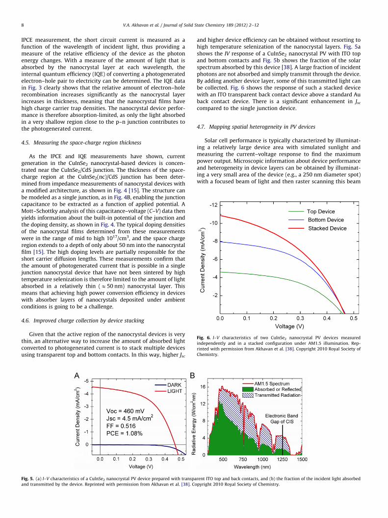
Fig. 6. I–V characteristics of two CuInSe2 nanocrystal PV devices measured
independently and in a stacked configuration under AM1.5 illumination. Rep-
rinted with permission from Akhavan et al. [38]. Copyright 2010 Royal Society of
Chemistry.
V.A. Akhavan et al. / Journal of Solid State Chemistry 189 (2012) 2–128
IPCE measurement, the short circuit current is measured as afunction of the wavelength of incident light, thus providing ameasure of the relative efficiency of the device as the photonenergy changes. With a measure of the amount of light that isabsorbed by the nanocrystal layer at each wavelength, theinternal quantum efficiency (IQE) of converting a photogeneratedelectron–hole pair to electricity can be determined. The IQE datain Fig. 3 clearly shows that the relative amount of electron–holerecombination increases significantly as the nanocrystal layerincreases in thickness, meaning that the nanocrystal films havehigh charge carrier trap densities. The nanocrystal device perfor-mance is therefore absorption-limited, as only the light absorbedin a very shallow region close to the p–n junction contributes tothe photogenerated current.
4.5. Measuring the space-charge region thickness
As the IPCE and IQE measurements have shown, currentgeneration in the CuInSe2 nanocrystal-based devices is concen-trated near the CuInSe2/CdS junction. The thickness of the space-charge region at the CuInSe2(nc)/CdS junction has been deter-mined from impedance measurements of nanocrystal devices witha modified architecture, as shown in Fig. 4 [15]. The structure canbe modeled as a single junction, as in Fig. 4B, enabling the junctioncapacitance to be extracted as a function of applied potential. AMott–Schottky analysis of this capacitance–voltage (C–V) data thenyields information about the built-in potential of the junction andthe doping density, as shown in Fig. 4. The typical doping densitiesof the nanocrystal films determined from these measurementswere in the range of mid to high 1017/cm3, and the space chargeregion extends to a depth of only about 50 nm into the nanocrystalfilm [15]. The high doping levels are partially responsible for theshort carrier diffusion lengths. These measurements confirm thatthe amount of photogenerated current that is possible in a singlejunction nanocrystal device that have not been sintered by hightemperature selenization is therefore limited to the amount of lightabsorbed in a relatively thin (E50 nm) nanocrystal layer. Thismeans that achieving high power conversion efficiency in deviceswith absorber layers of nanocrystals deposited under ambientconditions is going to be a challenge.
4.6. Improved charge collection by device stacking
Given that the active region of the nanocrystal devices is verythin, an alternative way to increase the amount of absorbed lightconverted to photogenerated current is to stack multiple devicesusing transparent top and bottom contacts. In this way, higher Jsc
Fig. 5. (a) I–V characteristics of a CuInSe2 nanocrystal PV device prepared with transpa
and transmitted by the device. Reprinted with permission from Akhavan et al. [38]. Co
and higher device efficiency can be obtained without resorting tohigh temperature selenization of the nanocrystal layers. Fig. 5ashows the IV response of a CuInSe2 nanocrystal PV with ITO topand bottom contacts and Fig. 5b shows the fraction of the solarspectrum absorbed by this device [38]. A large fraction of incidentphotons are not absorbed and simply transmit through the device.By adding another device layer, some of this transmitted light canbe collected. Fig. 6 shows the response of such a stacked devicewith an ITO transparent back contact device above a standard Auback contact device. There is a significant enhancement in Jsc
compared to the single junction device.
4.7. Mapping spatial heterogeneity in PV devices
Solar cell performance is typically characterized by illuminat-ing a relatively large device area with simulated sunlight andmeasuring the current–voltage response to find the maximumpower output. Microscopic information about device performanceand heterogeneity in device layers can be obtained by illuminat-ing a very small area of the device (e.g., a 250 nm diameter spot)with a focused beam of light and then raster scanning this beam
rent ITO top and back contacts, and (b) the fraction of the incident light absorbed
pyright 2010 Royal Society of Chemistry.
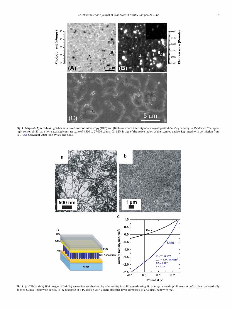
Fig. 7. Maps of (A) zero-bias light-beam induced current microscopy (LBIC) and (B) fluorescence intensity of a spray-deposited CuInSe2 nanocrystal PV device. The upper
right corner of (B) has a non-saturated contrast scale of 1,500 to 27,000 counts. (C) SEM image of the active region of the scanned device. Reprinted with permission from
Ref. [36]. Copyright 2010 John Wiley and Sons.
Fig. 8. (a) TEM and (b) SEM images of CuInSe2 nanowires synthesized by solution-liquid-solid growth using Bi nanocrystal seeds. (c) Illustration of an idealized vertically
aligned CuInSe2 nanowire device. (d) IV response of a PV device with a light-absorber layer composed of a CuInSe2 nanowire mat.
V.A. Akhavan et al. / Journal of Solid State Chemistry 189 (2012) 2–12 9
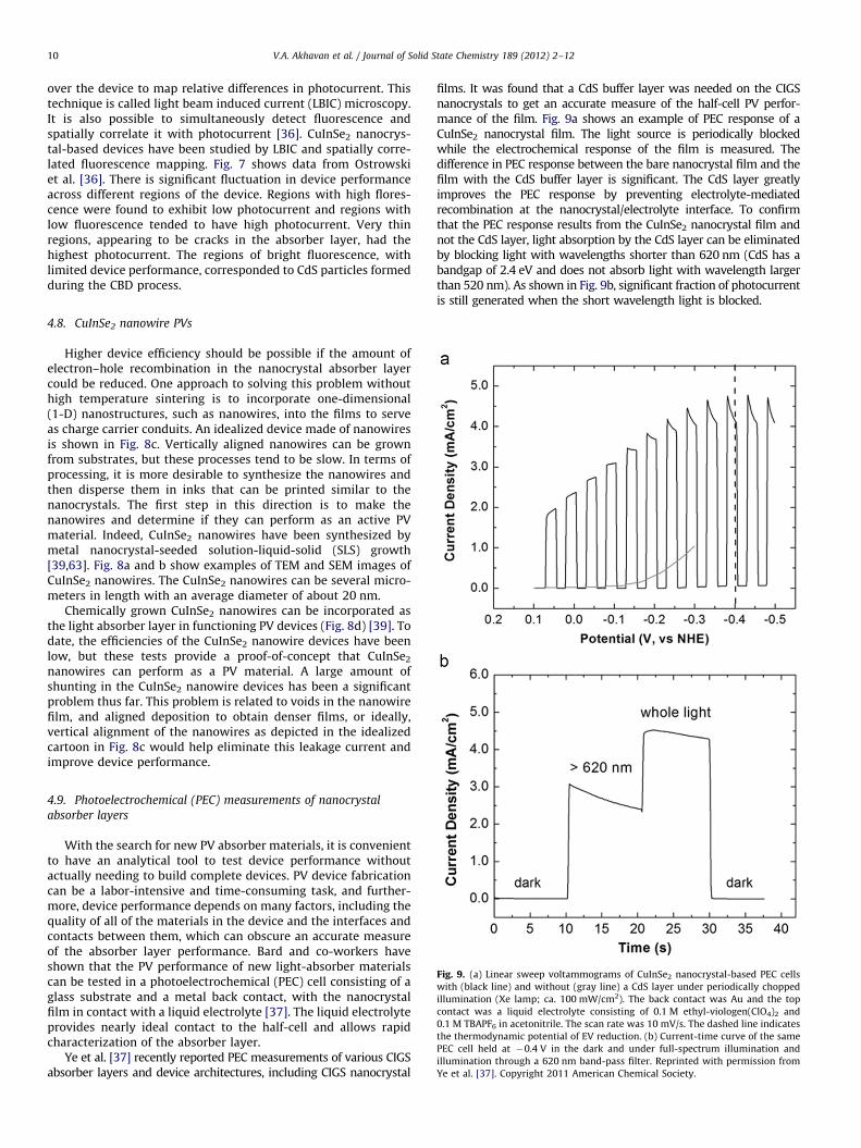
Fig. 9. (a) Linear sweep voltammograms of CuInSe2 nanocrystal-based PEC cells
with (black line) and without (gray line) a CdS layer under periodically chopped
illumination (Xe lamp; ca. 100 mW/cm2). The back contact was Au and the top
contact was a liquid electrolyte consisting of 0.1 M ethyl-viologen(ClO4)2 and
0.1 M TBAPF6 in acetonitrile. The scan rate was 10 mV/s. The dashed line indicates
the thermodynamic potential of EV reduction. (b) Current-time curve of the same
PEC cell held at �0.4 V in the dark and under full-spectrum illumination and
illumination through a 620 nm band-pass filter. Reprinted with permission from
Ye et al. [37]. Copyright 2011 American Chemical Society.
V.A. Akhavan et al. / Journal of Solid State Chemistry 189 (2012) 2–1210
over the device to map relative differences in photocurrent. Thistechnique is called light beam induced current (LBIC) microscopy.It is also possible to simultaneously detect fluorescence andspatially correlate it with photocurrent [36]. CuInSe2 nanocrys-tal-based devices have been studied by LBIC and spatially corre-lated fluorescence mapping. Fig. 7 shows data from Ostrowskiet al. [36]. There is significant fluctuation in device performanceacross different regions of the device. Regions with high flores-cence were found to exhibit low photocurrent and regions withlow fluorescence tended to have high photocurrent. Very thinregions, appearing to be cracks in the absorber layer, had thehighest photocurrent. The regions of bright fluorescence, withlimited device performance, corresponded to CdS particles formedduring the CBD process.
4.8. CuInSe2 nanowire PVs
Higher device efficiency should be possible if the amount ofelectron–hole recombination in the nanocrystal absorber layercould be reduced. One approach to solving this problem withouthigh temperature sintering is to incorporate one-dimensional(1-D) nanostructures, such as nanowires, into the films to serveas charge carrier conduits. An idealized device made of nanowiresis shown in Fig. 8c. Vertically aligned nanowires can be grownfrom substrates, but these processes tend to be slow. In terms ofprocessing, it is more desirable to synthesize the nanowires andthen disperse them in inks that can be printed similar to thenanocrystals. The first step in this direction is to make thenanowires and determine if they can perform as an active PVmaterial. Indeed, CuInSe2 nanowires have been synthesized bymetal nanocrystal-seeded solution-liquid-solid (SLS) growth[39,63]. Fig. 8a and b show examples of TEM and SEM images ofCuInSe2 nanowires. The CuInSe2 nanowires can be several micro-meters in length with an average diameter of about 20 nm.
Chemically grown CuInSe2 nanowires can be incorporated asthe light absorber layer in functioning PV devices (Fig. 8d) [39]. Todate, the efficiencies of the CuInSe2 nanowire devices have beenlow, but these tests provide a proof-of-concept that CuInSe2
nanowires can perform as a PV material. A large amount ofshunting in the CuInSe2 nanowire devices has been a significantproblem thus far. This problem is related to voids in the nanowirefilm, and aligned deposition to obtain denser films, or ideally,vertical alignment of the nanowires as depicted in the idealizedcartoon in Fig. 8c would help eliminate this leakage current andimprove device performance.
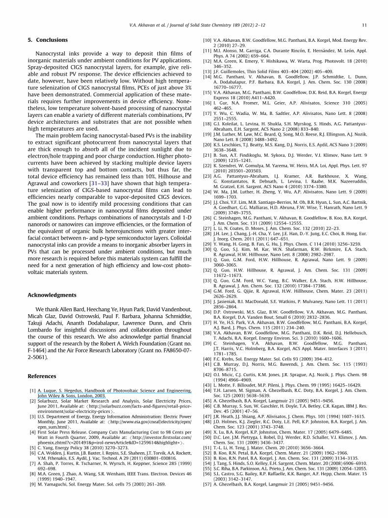
4.9. Photoelectrochemical (PEC) measurements of nanocrystal
absorber layers
With the search for new PV absorber materials, it is convenientto have an analytical tool to test device performance withoutactually needing to build complete devices. PV device fabricationcan be a labor-intensive and time-consuming task, and further-more, device performance depends on many factors, including thequality of all of the materials in the device and the interfaces andcontacts between them, which can obscure an accurate measureof the absorber layer performance. Bard and co-workers haveshown that the PV performance of new light-absorber materialscan be tested in a photoelectrochemical (PEC) cell consisting of aglass substrate and a metal back contact, with the nanocrystalfilm in contact with a liquid electrolyte [37]. The liquid electrolyteprovides nearly ideal contact to the half-cell and allows rapidcharacterization of the absorber layer.
Ye et al. [37] recently reported PEC measurements of various CIGSabsorber layers and device architectures, including CIGS nanocrystal
films. It was found that a CdS buffer layer was needed on the CIGSnanocrystals to get an accurate measure of the half-cell PV perfor-mance of the film. Fig. 9a shows an example of PEC response of aCuInSe2 nanocrystal film. The light source is periodically blockedwhile the electrochemical response of the film is measured. Thedifference in PEC response between the bare nanocrystal film and thefilm with the CdS buffer layer is significant. The CdS layer greatlyimproves the PEC response by preventing electrolyte-mediatedrecombination at the nanocrystal/electrolyte interface. To confirmthat the PEC response results from the CuInSe2 nanocrystal film andnot the CdS layer, light absorption by the CdS layer can be eliminatedby blocking light with wavelengths shorter than 620 nm (CdS has abandgap of 2.4 eV and does not absorb light with wavelength largerthan 520 nm). As shown in Fig. 9b, significant fraction of photocurrentis still generated when the short wavelength light is blocked.
V.A. Akhavan et al. / Journal of Solid State Chemistry 189 (2012) 2–12 11
5. Conclusions
Nanocrystal inks provide a way to deposit thin films ofinorganic materials under ambient conditions for PV applications.Spray-deposited CIGS nanocrystal layers, for example, give reli-able and robust PV response. The device efficiencies achieved todate, however, have been relatively low. Without high tempera-ture selenization of CIGS nanocrystal films, PCEs of just above 3%have been demonstrated. Commercial application of these mate-rials requires further improvements in device efficiency. None-theless, low temperature solvent-based processing of nanocrystallayers can enable a variety of different materials combinations, PVdevice architectures and substrates that are not possible whenhigh temperatures are used.
The main problem facing nanocrystal-based PVs is the inabilityto extract significant photocurrent from nanocrystal layers thatare thick enough to absorb all of the incident sunlight due toelectron/hole trapping and poor charge conduction. Higher photo-currents have been achieved by stacking multiple device layerswith transparent top and bottom contacts, but thus far, thetotal device efficiency has remained less than 10%. Hilhouse andAgrawal and coworkers [31–33] have shown that high tempera-ture selenization of CIGS-based nanocrystal films can lead toefficiencies nearly comparable to vapor-deposited CIGS devices.The goal now is to identify mild processing conditions that canenable higher performance in nanocrystal films deposited underambient conditions. Perhaps combinations of nanocrystals and 1-Dnanorods or nanowires can improve efficiencies, or the formation ofthe equivalent of organic bulk heterojunctions with greater inter-facial contact between n- and p-type semiconductor layers. Colloidalnanocrystal inks can provide a means to inorganic absorber layers inPVs that can be processed under ambient conditions, but muchmore research is required before this materials system can fulfill theneed for a next generation of high efficiency and low-cost photo-voltaic materials system.
Acknowledgments
We thank Allen Bard, Heechang Ye, Hyun Park, David Vandenbout,Micah Glaz, David Ostrowski, Paul F. Barbara, Johanna Schmidtke,Takuji Adachi, Ananth Dodabalapur, Lawrence Dunn, and ChrisLombardo for insightful discussions and collaboration throughoutthe course of this research. We also acknowledge partial financialsupport of the research by the Robert A. Welch Foundation (Grant no.F-1464) and the Air Force Research Laboratory (Grant no. FA8650-07-2-5061).
References
[1] A. Luque, S. Hegedus, Handbook of Photovoltaic Science and Engineering,John Wiley & Sons, London, 2003.
[2] Solarbuzz, Solar Market Research and Analysis, Solar Electricity Prices,June 2011, Available at: /http://solarbuzz.com/facts-and-figures/retail-price-environment/solar-electricity-pricesS.
[3] U.S. Department of Energy, Energy Information Administration: Electric PowerMonthly, June 2011, Available at: /http://www.eia.gov/cneaf/electricity/epm/epm_sum.htmlS.
[4] First Solar Press Release. Company Cuts Manufacturing Cost to 98 Cents perWatt in Fourth Quarter, 2009, Available at: /http://investor.firstsolar.com/phoenix.zhtml?c=201491&p=irol-newsArticle&ID=1259614&highlight=S.
[5] C. Yang, Energy Policy 38 (2010) 3270–3273.[6] C.A. Wolden, J. Kurtin, J.B. Baxter, I. Repins, S.E. Shaheen, J.T. Torvik, A.A. Rockett,
V.M. Fthenakis, E.S. Aydil, J. Vac. Technol. A 29 (2011) 030801–030816.[7] A. Shah, P. Torres, R. Tscharner, N. Wyrsch, H. Keppner, Science 285 (1999)
692–698.[8] M.A. Green, J. Zhao, A. Wang, S.R. Wenham, IEEE Trans. Electron. Devices 46
(1999) 1940–1947.[9] M. Yamaguchi, Sol. Energy Mater. Sol. cells 75 (2003) 261–269.
[10] V.A. Akhavan, B.W. Goodfellow, M.G. Panthani, B.A. Korgel, Mod. Energy Rev.2 (2010) 27–29.
[11] M.I. Alonso, M. Garriga, C.A. Durante Rincon, E. Hernandez, M. Leon, Appl.Phys. A 74 (2002) 659–664.
[12] M.A. Green, K. Emery, Y. Hishikawa, W. Warta, Prog. Photovolt. 18 (2010)346–352.
[13] J.F. Guillemoles, Thin Solid Films 403–404 (2002) 405–409.[14] M.G. Panthani, V. Akhavan, B. Goodfellow, J.P. Schmidtke, L. Dunn,
A. Dodabalapur, P.F. Barbara, B.A. Korgel, J. Am. Chem. Soc. 130 (2008)16770–16777.
[15] V.A. Akhavan, M.G. Panthani, B.W. Goodfellow, D.K. Reid, B.A. Korgel, EnergyExpress 18 (2010) A411–A420.
[16] I. Gur, N.A. Fromer, M.L. Geier, A.P. Alivisatos, Science 310 (2005)462–465.
[17] Y. Wu, C. Wadia, W. Ma, B. Sadtler, A.P. Alivisatos, Nano Lett. 8 (2008)2551–2555.
[18] G.I. Koleilat, L. Levina, H. Shukla, S.H. Myrskog, S. Hinds, A.G. Pattantyus-Abraham, E.H. Sargent, ACS Nano 2 (2008) 833–840.
[19] J.M. Luther, M. Law, M.C. Beard, Q. Song, M.O. Reese, R.J. Ellingson, A.J. Nozik,Nano Lett. 8 (2008) 3488–3492.
[20] K.S. Leschkies, T.J. Beatty, M.S. Kang, D.J. Norris, E.S. Aydil, ACS Nano 3 (2009)3638–3648.
[21] B. Sun, A.T. Findikoglu, M. Sykora, D.J. Werder, V.I. Klimov, Nano Lett. 9(2009) 1235–1241.
[22] K. Szendrei, W. Gomulya, M. Yarema, W. Heiss, M.A. Loi, Appl. Phys. Lett. 97(2010) 203501–203503.
[23] A.G. Pattantyus-Abraham, I.J. Kramer, A.R. Barkhouse, X. Wang,G. Konstantatos, R. Debnath, L. Levina, I. Raabe, M.K. Nazeeruddin,M. Gratzel, E.H. Sargent, ACS Nano 4 (2010) 3374–3380.
[24] W. Ma, J.M. Luther, H. Zheng, Y. Wu, A.P. Alivisatos, Nano Lett. 9 (2009)1699–1703.
[25] J.J. Choi, Y.F. Lim, M.B. Santiago-Berrios, M. Oh, B.R. Hyun, L. Sun, A.C. Bartnik,A. Goedhart, G.G. Malliaras, H.D. Abruna, F.W. Wise, T. Hanrath, Nano Lett. 9(2009) 3749–3755.
[26] C. Steinhagen, M.G. Panthani, V. Akhavan, B. Goodfellow, B. Koo, B.A. Korgel,J. Am. Chem. Soc. 131 (2009) 12554–12555.
[27] L. Li, N. Coates, D. Moses, J. Am. Chem. Soc. 132 (2010) 22–23.[28] J.H. Lee, J. Chang, J.-H. Cha, Y. Lee, J.E. Han, D.-Y. Jung, E.C. Choi, B. Hong, Eur.
J. Inorg. Chem. 2011 (2011) 647–651.[29] Y. Wang, H. Gong, B. Fan, G. Hu, J. Phys. Chem. C 114 (2010) 3256–3259.[30] Q. Guo, S.J. Kim, M. Kar, W.N. Shafarman, R.W. Birkmire, E.A. Stach,
R. Agrawal, H.W. Hillhouse, Nano Lett. 8 (2008) 2982–2987.[31] Q. Guo, G.M. Ford, H.W. Hillhouse, R. Agrawal, Nano Lett. 9 (2009)
3060–3065.[32] Q. Guo, H.W. Hillhouse, R. Agrawal, J. Am. Chem. Soc. 131 (2009)
11672–11673.[33] Q. Guo, G.M. Ford, W.C. Yang, B.C. Walker, E.A. Stach, H.W. Hillhouse,
R. Agrawal, J. Am. Chem. Soc. 132 (2010) 17384–17386.[34] G.M. Ford, G. Qijie, R. Agrawal, H.W. Hillhouse, Chem. Mater. 23 (2011)
2626–2629.[35] J. Jasieniak, B.I. MacDonald, S.E. Watkins, P. Mulvaney, Nano Lett. 11 (2011)
2856–2864.[36] D.P. Ostrowski, M.S. Glaz, B.W. Goodfellow, V.A. Akhavan, M.G. Panthani,
B.A. Korgel, D.A. Vanden Bout, Small 6 (2010) 2832–2836.[37] H. Ye, H.S. Park, V.A. Akhavan, B.W. Goodfellow, M.G. Panthani, B.A. Korgel,
A.J. Bard, J. Phys. Chem. 115 (2011) 234–240.[38] V.A. Akhavan, B.W. Goodfellow, M.G. Panthani, D.K. Reid, D.J. Hellebusch,
T. Adachi, B.A. Korgel, Energy Environ. Sci. 3 (2010) 1600–1606.[39] C. Steinhagen, V.A. Akhavan, B.W. Goodfellow, M.G. Panthani,
J.T. Harris, V.C. Holmberg, B.A. Korgel, ACS Appl. Mater. Interfaces 3 (2011)1781–1785.
[40] F.C. Krebs, Sol. Energy Mater. Sol. Cells 93 (2009) 394–412.[41] C.B. Murray, D.J. Norris, M.G. Bawendi, J. Am. Chem. Soc. 115 (1993)
8706–8715.[42] O.I. Micic, C.J. Curtis, K.M. Jones, J.R. Sprague, A.J. Nozik, J. Phys. Chem. 98
(1994) 4966–4969.[43] L. Motte, F. Billoudet, M.P. Pileni, J. Phys. Chem. 99 (1995) 16425–16429.[44] T.H. Larsen, M. Sigman, A. Ghezelbash, R.C. Doty, B.A. Korgel, J. Am. Chem.
Soc. 125 (2003) 5638–5639.[45] A. Ghezelbash, B.A. Korgel, Langmuir 21 (2005) 9451–9456.[46] C.B. Murray, S. Sun, W. Gaschler, H. Doyle, T.A. Betley, C.R. Kagan, IBM J. Res.
Dev. 45 (2001) 47–56.[47] J.R. Heath, J.J. Shiang, A.P. Alivisatos, J. Chem. Phys. 101 (1994) 1607–1615.[48] J.D. Holmes, K.J. Ziegler, R.C. Doty, L.E. Pell, K.P. Johnston, B.A. Korgel, J. Am.
Chem. Soc. 123 (2001) 3743–3748.[49] X. Lu, B.A. Korgel, K.P. Johnston, Chem. Mater. 17 (2005) 6479–6485.[50] D.C. Lee, J.M. Pietryga, I. Robel, D.J. Werder, R.D. Schaller, V.I. Klimov, J. Am.
Chem. Soc. 131 (2009) 3436–3437.[51] T.-L. Li, H. Teng, J. Mater. Chem. 20 (2010) 3656–3664.[52] B. Koo, R.N. Petal, B.A. Korgel, Chem. Mater. 21 (2009) 1962–1966.[53] B. Koo, R.N. Patel, B.A. Korgel, J. Am. Chem. Soc. 131 (2009) 3134–3135.[54] J. Tang, S. Hinds, S.O. Kelley, E.H. Sargent, Chem. Mater. 20 (2008) 6906–6910.[55] S.C. Riha, B.A. Parkinson, A.L. Prieto, J. Am. Chem. Soc. 131 (2009) 12054–12055.[56] S.L. Castro, S.G. Bailey, R.P. Raffaelle, K.K. Banger, A.F. Hepp, Chem. Mater. 15
(2003) 3142–3147.[57] A. Ghezelbash, B.A. Korgel, Langmuir 21 (2005) 9451–9456.

V.A. Akhavan et al. / Journal of Solid State Chemistry 189 (2012) 2–1212
[58] C. Wadia, A.P. Alivisatos, D.M. Kammen, Environ. Sci. Technol. 43 (2009)2072–2077.
[59] T.K. Todorov, K.B. Reuter, D.B. Mitzi, Adv. Mater. 22 (2010) E156–E159.[60] Y. Hashimoto, N. Kohara, T. Negami, N. Nishitani, T. Wada, Sol. Energy Mater.
Sol. Cells 50 (1998) 71–77.
[61] T. Schulmeyer, R. Kniese, R. Hunger, W. Jaegermann, M. Powalla, A. Klein,Thin Solid Films 451–452 (2004) 420–423.
[62] U. Rau, H.W. Schock, Appl. Phys. A 69 (1999) 131–147.[63] A.J. Wooten, D.J. Werder, D.J. Williams, J.L. Casson, J.A. Hollingsworth, J. Am.
Chem. Soc. 131 (2009) 16177–16188.